EP2084735B1 - Temperaturgeregelte mehrfach-gasverteilerbaugruppe - Google Patents
Temperaturgeregelte mehrfach-gasverteilerbaugruppe Download PDFInfo
- Publication number
- EP2084735B1 EP2084735B1 EP07844101.1A EP07844101A EP2084735B1 EP 2084735 B1 EP2084735 B1 EP 2084735B1 EP 07844101 A EP07844101 A EP 07844101A EP 2084735 B1 EP2084735 B1 EP 2084735B1
- Authority
- EP
- European Patent Office
- Prior art keywords
- channels
- lid assembly
- gas
- manifold
- lid
- Prior art date
- Legal status (The legal status is an assumption and is not a legal conclusion. Google has not performed a legal analysis and makes no representation as to the accuracy of the status listed.)
- Active
Links
Images


Classifications
-
- C—CHEMISTRY; METALLURGY
- C23—COATING METALLIC MATERIAL; COATING MATERIAL WITH METALLIC MATERIAL; CHEMICAL SURFACE TREATMENT; DIFFUSION TREATMENT OF METALLIC MATERIAL; COATING BY VACUUM EVAPORATION, BY SPUTTERING, BY ION IMPLANTATION OR BY CHEMICAL VAPOUR DEPOSITION, IN GENERAL; INHIBITING CORROSION OF METALLIC MATERIAL OR INCRUSTATION IN GENERAL
- C23C—COATING METALLIC MATERIAL; COATING MATERIAL WITH METALLIC MATERIAL; SURFACE TREATMENT OF METALLIC MATERIAL BY DIFFUSION INTO THE SURFACE, BY CHEMICAL CONVERSION OR SUBSTITUTION; COATING BY VACUUM EVAPORATION, BY SPUTTERING, BY ION IMPLANTATION OR BY CHEMICAL VAPOUR DEPOSITION, IN GENERAL
- C23C16/00—Chemical coating by decomposition of gaseous compounds, without leaving reaction products of surface material in the coating, i.e. chemical vapour deposition [CVD] processes
- C23C16/44—Chemical coating by decomposition of gaseous compounds, without leaving reaction products of surface material in the coating, i.e. chemical vapour deposition [CVD] processes characterised by the method of coating
- C23C16/455—Chemical coating by decomposition of gaseous compounds, without leaving reaction products of surface material in the coating, i.e. chemical vapour deposition [CVD] processes characterised by the method of coating characterised by the method used for introducing gases into reaction chamber or for modifying gas flows in reaction chamber
- C23C16/45563—Gas nozzles
- C23C16/45565—Shower nozzles
-
- C—CHEMISTRY; METALLURGY
- C23—COATING METALLIC MATERIAL; COATING MATERIAL WITH METALLIC MATERIAL; CHEMICAL SURFACE TREATMENT; DIFFUSION TREATMENT OF METALLIC MATERIAL; COATING BY VACUUM EVAPORATION, BY SPUTTERING, BY ION IMPLANTATION OR BY CHEMICAL VAPOUR DEPOSITION, IN GENERAL; INHIBITING CORROSION OF METALLIC MATERIAL OR INCRUSTATION IN GENERAL
- C23C—COATING METALLIC MATERIAL; COATING MATERIAL WITH METALLIC MATERIAL; SURFACE TREATMENT OF METALLIC MATERIAL BY DIFFUSION INTO THE SURFACE, BY CHEMICAL CONVERSION OR SUBSTITUTION; COATING BY VACUUM EVAPORATION, BY SPUTTERING, BY ION IMPLANTATION OR BY CHEMICAL VAPOUR DEPOSITION, IN GENERAL
- C23C16/00—Chemical coating by decomposition of gaseous compounds, without leaving reaction products of surface material in the coating, i.e. chemical vapour deposition [CVD] processes
- C23C16/44—Chemical coating by decomposition of gaseous compounds, without leaving reaction products of surface material in the coating, i.e. chemical vapour deposition [CVD] processes characterised by the method of coating
- C23C16/455—Chemical coating by decomposition of gaseous compounds, without leaving reaction products of surface material in the coating, i.e. chemical vapour deposition [CVD] processes characterised by the method of coating characterised by the method used for introducing gases into reaction chamber or for modifying gas flows in reaction chamber
- C23C16/45563—Gas nozzles
- C23C16/45572—Cooled nozzles
-
- C—CHEMISTRY; METALLURGY
- C23—COATING METALLIC MATERIAL; COATING MATERIAL WITH METALLIC MATERIAL; CHEMICAL SURFACE TREATMENT; DIFFUSION TREATMENT OF METALLIC MATERIAL; COATING BY VACUUM EVAPORATION, BY SPUTTERING, BY ION IMPLANTATION OR BY CHEMICAL VAPOUR DEPOSITION, IN GENERAL; INHIBITING CORROSION OF METALLIC MATERIAL OR INCRUSTATION IN GENERAL
- C23C—COATING METALLIC MATERIAL; COATING MATERIAL WITH METALLIC MATERIAL; SURFACE TREATMENT OF METALLIC MATERIAL BY DIFFUSION INTO THE SURFACE, BY CHEMICAL CONVERSION OR SUBSTITUTION; COATING BY VACUUM EVAPORATION, BY SPUTTERING, BY ION IMPLANTATION OR BY CHEMICAL VAPOUR DEPOSITION, IN GENERAL
- C23C16/00—Chemical coating by decomposition of gaseous compounds, without leaving reaction products of surface material in the coating, i.e. chemical vapour deposition [CVD] processes
- C23C16/44—Chemical coating by decomposition of gaseous compounds, without leaving reaction products of surface material in the coating, i.e. chemical vapour deposition [CVD] processes characterised by the method of coating
- C23C16/455—Chemical coating by decomposition of gaseous compounds, without leaving reaction products of surface material in the coating, i.e. chemical vapour deposition [CVD] processes characterised by the method of coating characterised by the method used for introducing gases into reaction chamber or for modifying gas flows in reaction chamber
- C23C16/45563—Gas nozzles
- C23C16/45574—Nozzles for more than one gas
Definitions
- the invention relates to an apparatus for processing substrates, such as semiconductor wafers, and more particularly, to an apparatus for distribution of process fluids over a substrate.
- Semiconductor processing systems generally include a process chamber having a pedestal for supporting a substrate, such as a semiconductor wafer, within the chamber proximate a processing region.
- the chamber forms a vacuum enclosure defining, in part, the processing region.
- a gas distribution assembly or showerhead provides one or more process gases to the processing region. The gases are then heated and/or energized to form a plasma which performs certain processes upon the substrate. These processes may include deposition processes, such as chemical vapor deposition (CVD), to deposit a film upon the substrate or an etch reaction to remove material from the substrate, among other processes.
- CVD chemical vapor deposition
- Document EP 1 168 420 describes a gas supply nozzle plate which is constructed by laminating a plurality of metal members each having a fluid path and branch.
- a fluid nozzle plate member has high sealing at a joined part, and high reliability even when used in high vacuum or at a high temperature.
- the fluid nozzle plate member comprises a plurality of plate-like metal members each having a fluid path and/or a branch. In this case, the plurality of plate-like metal members are laminated, and the laminated surfaces thereof are joined together by press forging.
- US 6,444,039 B1 describes a vapor supply apparatus, for use in a semiconductor device manufacturing process.
- the vapor supply apparatus provides a three-dimensional showerhead for supplying various precursors to a reaction chamber.
- the three-dimensional showerhead comprises an inverted-cup structure having double walls, an outer wall and an inner wall, with the double walls defining a first interior volume and the inner wall defining an exterior cavity, the inverted-cup structure further has a plurality of first inlet ports connected to the outer wall for introducing first precursors into the first interior volume and a plurality of first outlet ports at the inner wall for discharging the first precursor vapor from the first interior volume to the exterior cavity.
- the three-dimensional showerhead confines the precursor vapor inside the external cavity to modify the processed film characteristics
- the gases may be combined within a mixing chamber that is then coupled to the gas distribution assembly via a conduit.
- a conventional thermal CVD process two process gases are supplied to a mixing chamber along with two respective carrier gases where they are combined to form a gaseous mixture.
- the gaseous mixture may be introduced directly to the chamber, or may travel through a conduit within an upper portion of the chamber to the distribution assembly.
- the distribution assembly generally includes a plate having a plurality of holes such that the gaseous mixture is evenly distributed into the processing region above the substrate.
- two gases pass through the distribution assembly separately, and allowed to combine before reaching the processing region and/or the substrate. As the gaseous mixture enters the processing region and is infused with thermal energy, a chemical reaction occurs between the process gases, resulting in a chemical vapor deposition reaction on the substrate.
- the gases tend to begin reduction, or otherwise react, within the mixing chamber or distribution plate. Consequently, deposition on or etching of the mixing chamber, conduits, distribution plate, and other chamber components may result prior to the gaseous mixture reaching the processing region. Additionally, reaction by products may accumulate in the chamber gas delivery components or on the inside surface of the distribution plate, thus generating, and/or increasing the presence of, unwanted particles.
- Temperature control of the gases as they are released into the processing region is advantageous for controlling the reactivity of the gases. For example, cooling the gases can be helpful in controlling unwanted reactions prior to release into the processing region. The gases refrain from reacting until they come into contact with a heated substrate. In other circumstances, heating of gases may be necessary. For example, hot gas purging or cleaning may help remove contaminants from a processing chamber. Thus, integrating a temperature control aspect into a gas distribution plate is useful.
- gas distribution devices While some gas distribution devices have been developed to minimize gas mixing prior to entry into the processing region, the devices may tend to prematurely deteriorate during processing.
- conventional distribution devices may be made of materials that expand and contract during processing, leading to deterioration of the device or other parts of the processing chamber.
- the conventional devices may also require sealing with large elastomeric seals, such as large diameter o-rings that may deteriorate over time, which may lead to leaks within the device.
- conventional devices that deliver two or more gases to the processing region may not mix uniformly in the processing region, thus leading to non-uniform deposition on the substrate.
- Embodiments described herein relate to an apparatus and method for delivering process fluids to a processing chamber for deposition of a film on a substrate, etching a substrate, and other processes.
- an apparatus for delivering a process fluid to a processing chamber includes a first manifold having a plurality of isolated fluid channels at least partially formed therein, and a second manifold coupled to the first manifold, wherein a portion of the plurality of isolated fluid channels include a first and second gas channel in communication with the second manifold.
- a lid assembly for a processing chamber comprises an upper manifold having fluidly isolated first and second flow paths defined therethrough, and a lower manifold with a top side coupled to the upper manifold, and a bottom side having a first plurality of outlets fluidly coupled to the first flow path and a second plurality of outlets fluidly coupled to the second flow path, respectively, wherein the lower manifold comprises a plurality of concentric rings having an inner surface in sealing contact with an outer surface of an adjoining ring adapted to form a material to material seal therebetween.
- an apparatus for delivering a process fluid to a processing chamber includes a manifold assembly with a top side and a bottom side, the top side having a plurality of fluidly isolated circular channels partially formed thereon, and the bottom side having annular outlets formed therein; and a lid plate having a top, a bottom, and an edge, wherein the bottom of the lid plate is coupled to the top side of the manifold assembly, and the lid plate has at least two gas passages and a plurality of thermal control fluid passages formed therethrough in fluid communication with the plurality of circular channels.
- a lid assembly for a processing chamber includes an upper manifold having a plurality of fluidly isolated channels partially formed therein, and a lower manifold coupled to the upper manifold, wherein a first portion of the plurality of fluidly isolated channels comprise first and second gas channels in fluid communication with the lower manifold, and a second portion of the plurality of fluidly isolated channels comprise a plurality of thermal control channels.
- an apparatus for delivering a process fluid to a processing chamber includes a manifold assembly with a top side and a bottom side, the top side having a plurality of fluidly isolated circular channels partially formed thereon, and the bottom side having annular outlets formed therein, and a lid plate having a top, a bottom, and an edge, wherein the bottom of the lid plate is coupled to the top side of the manifold assembly, and the lid plate has at least two gas passages and a plurality of thermal control fluid passages formed therethrough in fluid communication with the plurality of circular channels.
- a method for making a gas distribution plate includes providing a lid plate having a plurality of radial gas passages formed therein, providing a first manifold having a plurality of circular channels formed therein, wherein a portion of the plurality of circular channels define first and second gas channels, providing a second manifold having a plurality of annular grooves formed therein, wherein a the first and second gas channels are in fluid communication with the plurality of annular grooves, and coupling the first and second manifolds to form a gas distribution plate.
- FIG. 1 is a cross-sectional view of one embodiment of a processing chamber 100.
- the processing chamber 100 includes a substrate support 102 disposed within an interior volume 101.
- a substrate 104 such as a semiconductor wafer, may enter and exit the interior volume 101 by an opening 103 disposed in a wall of the processing chamber 100.
- Chamber 100 also includes a lid assembly 105 coupled to an upper surface thereof, which forms a boundary for at least a portion of the interior volume 101.
- lid assembly 105 comprises a lid plate 112, an upper manifold 113 in fluid communication with lid plate 112, a lower manifold 114 in fluid communication with upper manifold 113, and a lid ring 115.
- a lower surface of the lid assembly 105 and the upper surface of the substrate 104 define a processing region 106.
- Lower manifold 114 of lid assembly 105 is in fluid communication with processing region 106.
- the processing chamber 100 includes an annular member, such as a shadow ring 109, which circumscribes a portion of the substrate support 102 adjacent the substrate 104.
- the shadow ring 109 is adapted to contact the substrate support 102 as the substrate support is raised to a processing position.
- a peripheral portion of the shadow ring 109 substantially isolates the lower portion of the substrate support 102 from the processing region 106. This isolation prevents or minimizes the introduction of process gases in portions of the interior volume 101.
- the reduction in the volume of the interior volume 101, as defined by the processing region 106 reduces the volume of process gases provided to the processing chamber 100.
- the volume of processing region 106 is defined by the distance between the top surface of substrate 104 and the lowest surface of lid 105.
- Substrate support 102 may be raised and lowered before and after processing to allow entry and exit of substrates. Vacuum is maintained in, and any undeposited gases are evacuated from, process chamber 101 through annular vacuum channel 124 and vacuum portal 111, which is coupled to a vacuum pump (not shown).
- Substrate support 102 may be formed of conducting or non-conducting materials, such as a metal (e.g. aluminum, steel, stainless steel, nickel, chromium, an alloy thereof or combinations thereof) or ceramic material.
- substrate 104 may be heated to a desired temperature prior to and/or during a pretreatment step, a deposition step, post-treatment step or other process step used during the fabrication process.
- substrate support 102 may be heated using an embedded heating element (not shown) such as a resistance heater or a conduit formed within substrate support 102 to supply a heating fluid.
- substrate support 102 may be heated using radiant heaters such as, for example, lamps (not shown).
- Temperature sensors such as one or more thermocouples (not shown), may also be embedded in substrate support 102 to monitor the temperature of substrate support 102. The measured temperature may be used in a feedback loop to control a power supply for the heating element, such that the temperature of substrate 104 may be maintained or controlled at a desired temperature which is suitable for the particular process application.
- Substrate lift pins (not shown) may also be disposed in substrate support 102 and are used to raise and lower substrate 104 from the support surface to facilitate transfer of the substrate into and out of the processing chamber 100.
- fluids such as gases
- valve 107A is adapted to couple with a process fluid source F 1 .
- Valve 107A may be any control valve for controlling fluid or gas flow, such as a pneumatically, magnetically, or electrically-actuated valve.
- Control valves may be biased open or closed, and actuated open or closed in short intervals to provide pulses of gases or continuous streams. Suitable valves are available from Fujikin, Inc., of Osaka, Japan, and Veriflo Corp., of Richmond, California.
- Atomic layer deposition (ALD) processes utilize control valves, such as the valve 107A, to generate pulses of gas to the processing region 106.
- valve 107A may be configured to provide an opened/closed cycle within a range from 10 milliseconds to 5 seconds.
- the valve may be quickly pulsed for less than about 1 second, such as within a range from about 10 milliseconds to about 1 second, for example, from about 50 milliseconds to 700 milliseconds, or from about 100 milliseconds to about 500 milliseconds.
- the valve may be pulsed slower, such as for more than about 1 second, such as within a range from about 1 second to about 5 seconds, for example, from about 1.5 seconds to 4 seconds, or from about 2 seconds to about 3 seconds.
- FIG 2 is a cross-sectional view of another embodiment of processing chamber 100 of Figure 1 that has been rotated along a longitudinal axis.
- the lid assembly also includes inlet 200.
- Inlet 200 is adapted to couple with valve 107B, which in turn is coupled with a fluid source F 2 that is distinct from the source F 1 coupled with valve 107A ( Figure 1 ).
- valve 107B and 107A are separate but similar, each capable of providing pulses or continuous flow of fluids or gases as described above. Such a system can be used to flow two gases simultaneously through two separated flow paths.
- Embodiments with more than two gas pathways are also contemplated by extension from the embodiment shown by Figures 1 and 2 .
- inventions shown in Figures 1 and 2 can be configured to deposit material on a substrate during an atomic layer deposition (ALD) process, chemical vapor deposition (CVD) process, or a metal-organic or organic-metallic CVD (MOCVD or OMCVD) process.
- ALD atomic layer deposition
- CVD chemical vapor deposition
- MOCVD metal-organic or organic-metallic CVD
- embodiments described herein may be used in high or low pressure processes, high or low temperatures, and with continuous or pulsed, simultaneous or alternating gas flow.
- Fluid sources F 1 and F 2 coupled to valves 107A, 107B may provide metal halides, such as hafnium tetrachloride (HfCl 4 ), tungsten hexafluoride (WF 6 ), or tungsten hexachloride (WCl 6 ), metal carbonyls, such as tungsten carbonyl (W(CO) 6 ), reducing compounds, such as ammonia (NH 3 ), hydrogen ( i.e .
- metal halides such as hafnium tetrachloride (HfCl 4 ), tungsten hexafluoride (WF 6 ), or tungsten hexachloride (WCl 6 )
- metal carbonyls such as tungsten carbonyl (W(CO) 6 )
- reducing compounds such as ammonia (NH 3 )
- NH 3 ammonia
- hydrogen i.e .
- Substrates on which embodiments of the invention may be useful include, but are not limited to semiconductor wafers, such as crystalline silicon (e.g., Si ⁇ 100> or Si ⁇ 111>), silicon oxide, strained silicon, silicon nitride, silicon germanium, germanium, gallium arsenide, glass, sapphire, metals, metal alloys, metal nitrides, doped or undoped polysilicon, doped or undoped silicon wafers and patterned or non-patterned wafers.
- Substrates may be exposed to a pretreatment process to polish, etch, reduce, oxidize, hydroxylate, anneal and/or bake the substrate surface.
- one embodiment of the lid assembly 105 includes a lid plate 112, a first or upper manifold 113, a second or lower manifold 114, and a lid ring 115.
- the lid plate 112 includes two lateral conduits, such as passage 117 and 202 that are in fluid communication with processing region 106 through upper manifold 113 and lower manifold 114.
- the passages 117, 202 may be radially arranged in different planes of the lid plate 112.
- the lid plate 112 may be formed by any suitable means, such as machining, casting, molding, brazing welding, or a combination thereof.
- Passages 117 and 202 may be formed in lid plate 112 by any conventional means, including drilling and milling and, in one embodiment, are offset by about 45 degrees and are spaced above and below each other. In one embodiment, passages 117 and 202 are formed by using a gun-drill.
- the lid plate 112 may be formed from materials such as aluminum, stainless steel, nickel, alloys or combinations thereof, or a ceramic material. In one embodiment, when passages 117 and 202 are drilled, the open end of the passages 117, 202 are sealed by plugs 118 and 203. Plugs 118, 203 may be formed from a metal, such as those listed above, ceramic, or organic or inorganic polymer material. Plugs 118, 203 are typically made of a material having a similar coefficient of expansion as the material of lid plate 112. Other methods of forming inlets and manifolds in lid plate 112, such as casting, welding, or brazing, may not require plugs to prevent gas escaping.
- lid plate 112 includes two gas inputs 116 and 200 fluidly coupled to valves 107A, 107B, through which two fluids, which may be in gas or vapor phase, are introduced to chamber 100.
- the inputs 116 and 200 are connected to passages 117 and 202, respectively, which are in fluid communication with processing region 106.
- gas from source F 1 passes through valve 107A coupled with input 116 into passage 117.
- Gas from source F 1 then passes from passage 117 into openings 220A and flows into channels 119 formed in the upper manifold 113.
- Gas from source F 2 passes through valve 107B coupled with input 200 into passage 202.
- Gas from source F 2 then passes from passage 202 into opening 220B and flows into channels 204 formed in the upper manifold 113, and as gas from sources F 1 and F 2 reach upper manifold 113, the gases remain separated in two distinct flow paths.
- upper gas channels 119 and 204 are arranged in a pattern of circular channels in upper manifold 113.
- the circular channels 119, 204 are coupled to the lower manifold through holes 205A and 205B, as will be explained in detail below.
- Figure 3A is a top view of one embodiment of upper manifold 113.
- Upper manifold 113 includes a plurality fluid channels 301 disposed between and isolated from upper gas channels 119 and 204.
- the upper manifold 113 also includes a plurality of outer fluid channels 302.
- Each of the fluid channels 301, 302 provide a conduit for a thermal control fluid to be flowed therein, thus providing enhanced thermal control of the upper manifold 113.
- Thermal control fluid may be in a liquid or gas.
- Liquids that may be used include water, such as de-ionized water, oil, alcohols, glycols, glycol ethers, other organic solvents, supercritical fluids ( e.g ., CO 2 ) derivatives thereof or mixtures thereof.
- Gases may include nitrogen, argon, air, hydrofluorocarbons (HFCs), or combinations thereof.
- Thermal control fluids enter and exit upper manifold 113 through ports 401, 402 ( Figures 3B , 3C , and 4A ) formed in lid plate 112.
- the upper manifold 113 is made of process resistant and/or chemistry compatible materials, such as aluminum, stainless steel, a ceramic material, or combinations thereof.
- the upper manifold 113 may be molded, cast, machined, or a combination thereof.
- lid plate 112 and upper manifold 113 may be brazed together to form a singular plate with gas delivery and thermal control features integrated.
- the mating surfaces of the upper manifold 113 and lid plate 112 form a shear seal. The surfaces may be finished by lapping or other suitable technique.
- Each of the upper gas channels 119, 204 and fluid channels 301, 302 define conduits having one side adapted to be sealed by a lower surface of the lid plate 112 when coupled thereto.
- Upper gas channels 119, 204 and fluid channels 301, 302 may have a cross-sectional shape including U-shaped having rounded corners, a U-shape having substantially square corners, or a combination thereof.
- each of the upper gas channels 119, 204 are separated by fluid channels 301.
- Annular walls between upper gas channels 119, 204 and fluid channels 301 provide separate flow paths for respective gases and fluids.
- the upper gas channels 119, 204 and fluid channels 301, 302 are separated and sealed when the lid plate 112 is coupled to the upper manifold 113 to prevent contamination between the thermal control fluid and the gases.
- fluid channels 301, 302, and gas channels 119, 204 are not limited to the number and configuration as shown. Greater or fewer fluid channels 301, 302, and gas channels 119, 204 may be used, and the shape of the fluid channels 301, 302, and gas channels 119, 204 may be formed in the upper manifold 113 in any shape desired. For example, more inner channels 301 and fewer outer channels 302 may be used, or vice versa. Other embodiments may have channels with different cross-sectional shapes, such as complete circles. Still other embodiments may include more vertical configurations, such as layers of channels formed within one of the lid plate 112 and/or upper manifold 113.
- Figure 3B is a schematic top view of upper manifold 113 showing the position of passage 117 in relation to gas channels 119.
- fluid channels 301, 302 are shown in phantom, and gas channels 204 are not shown, for clarity.
- openings 220A of passage 117 are in fluid communication with gas channels 119.
- Holes 205A which are in fluid communication with lower manifold 114, are positioned at about a 45 degree offset from the openings 220A.
- gas from source F 1 may be introduced through valve 107A, flow through gas channels 119, and be delivered to lower manifold 114 without mixing with gas from source F 2 and thermal control fluids.
- the embodiment is not limited to the number and positioning of holes 205A as more or less holes 205A may be added at different radial positions and/or different angular offsets within the gas channels 119.
- Figure 3C is a schematic top view of upper manifold 113 showing the position of passage 202 in relation to gas channels 204.
- fluid channels 301, 302 are shown in phantom, and gas channels 119 are not shown, for clarity.
- openings 220B of passage 202 are in fluid communication with gas channels 204.
- Holes 205B which are in fluid communication with lower manifold 114, are positioned at about a 45 degree offset from the openings 220B.
- gas from source F 2 may be introduced through valve 107B, flow through gas channels 204, and be delivered to lower manifold 114 without mixing with gas from source F 1 and thermal control fluids.
- the embodiment is not limited to the number and positioning of holes 205B as more or less holes 205B may be added at different radial positions and/or different angular offsets within the gas channels 204.
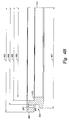
- FIG 4A is an exploded isometric view of one embodiment of a lid assembly 105.
- Lower manifold 114 is shown exploded into its constituent nested rings 121 and 206, which, when assembled, form lower manifold 114.
- rings 121, 206 are precision-manufactured to seal without the use of o-rings, gaskets, or the like.
- the rings 121, 206 form a shear seal between portions of inner and outer diameters that are in contact.
- the rings 121, 206 may be formed by lapping and inner and outer diameters of each ring 121, 206 are held to tolerances wherein a material to material seal is formed at points where the rings contact.
- the material to material seal provides a substantial gas-tight seal that prevents and/or minimizes leakage between gas passages defined between rings 121, 206.
- Apertures 123 and 207 in rings 121 and 206 are in fluid communication with channels 119 and 204 of upper manifold 113 via openings 205A, 205B, respectively.
- gas from inputs 116 and 200 of lid plate 112 flows through upper manifold 113 into lower manifold 114.
- Gases from sources F 1 and F 2 flow through inputs 116 and 200, respectively, of lid plate 112.
- Thermal cooling fluids flow through portals 401 and 402 of lid plate 112.
- the arrangement of openings and passages in the various components may be varied in numerous ways to create different embodiments. For example, more openings may be provided in any geometrically optimum pattern. Likewise, openings may be aligned, as shown in the figures, or they may be staggered. Openings may also be sized to optimize flow and pressure distributions throughout the apparatus.
- Figure 4B is a partial cross-sectional schematic of one embodiment of a ring 206, which is similar in construction to ring 121.
- ring 206 is precision-ground, lapped, or polished along inner and outer diameters to create a shear seal with the mating ring to minimize and/or prevent gas leaking through lower manifold 114.
- Ring 206 has an extended top portion 408 that forms a ledge around the perimeter of the ring.
- the aperture 207 is formed through the top portion 408.
- the top portion 408 is defined by a first outer radius 403 and a first inner radius 405, measured with reference to the centerline 411 of the ring.
- the ring 206 also includes a bottom portion defined by a second outer radius 407 and a second inner radius 406.
- Each ring 206 also includes a gap 208 defined by a third outer radius 404.
- the difference of the first inner radius 405 and second inner radius 406 result in a shoulder 410 being defined on the inside of the ring 206.
- the radii described above in reference to ring 206 may be varied to form different embodiments of rings 121 and 206.
- Rings 121 and 206 may be formed from hard materials that withstand temperatures in excess of 1000 degrees C with a low coefficient of thermal expansion.
- the materials may be hard materials, such as silicon carbide, silicon graphite, sapphire, quartz, a ceramic material or other hard materials.
- each ring comprises a first outer diameter and a second outer diameter, having a third outer diameter therebetween, wherein the third diameter is the gap 208.
- Each ring also comprises a first inner diameter and a second inner diameter to form a shoulder 410.
- the first outer diameter of one ring is adapted to press or slip-fit with the first inner diameter of another ring.
- the rings 121, 206 are adapted to fit together to form lower manifold 114 wherein the extended top portion 408 of one ring abuts the shoulder area 410 of another ring.
- the first outer radius 403 of one ring measured from the centerline 411, is slightly less than the first inner radius 405 of another ring, wherein the diameters of the constituent rings enable a press-fit. The difference between the first inner diameter and the second inner diameter, and the surface finish of the rings, enable a material to material seal to produce a substantial gas-tight seal between adjacent rings.
- annular groove 501 As the rings 121, 206 are sequentially fitted together, the difference between the second outer radius 407 of one ring and second inner radius 406 of an adjacent ring form annular groove 501 ( Figure 5 ).
- the width of annular groove 501 is generally between about 0.010 mils to about 0.060 mils, such as about 0.030 mils.
- Annular groove 501 is in fluid communication with gap 208, which is in communication with upper manifold 113 via aperture 207.
- FIG. 5 shows a detailed cross-section view of lid assembly 105.
- the shape of rings 121 and 206 are formed to include annular gaps 122 and 208 as described above. Annular gaps 122 and 208 are in fluid communication with annular grooves 501, which are in fluid communication with processing region 106.
- lower manifold 114 couples with lid plate 115, which comprises additional water conduits 505, and a containment ring 506.
- the lid assembly is sealed around a perimeter and various interior portions using o-rings 507, in the locations indicated.
- annular grooves 501 terminate in an annular nozzle 502.
- geometry of annular nozzles 502 may be designed to create a specific spread pattern of gas within processing volume 106. This spread pattern, substantially triangular or trapezoidal in cross-sectional shape, creates a separation zone 503 and a mixing zone 504, wherein the distinct gases G 1 and G 2 from sources F 1 and F 2 are not mixed until reaching the mixing zone 504. This enables enhanced control of reactive species within processing volume 106, which may eliminate or minimize any unwanted deposition on surfaces other than substrate 104.
- the sidewalls of the nozzles 502 may be angled from about 15 degrees to about 90 degrees, such as about 50 degrees to about 70 degrees, for example, about 60 degrees.
- the surface of the nozzles 502 may be modified to change the flow attributes and/or the geometry of the spread pattern and enhance flow characteristics.
- the surface may be roughened to facilitate a more laminar flow.
- the surface may be smoothed or not roughened to provide a faster, more turbulent flow of gasses.
- the nozzles 502 may include a surface that has been bead, ice, or grit blasted.
- gas from source F 1 passes through valve 107A coupled with input 116 into passage 117. Gas from source F 1 then passes from passage 117 into opening 220A for introduction into the upper manifold 113. Gas from source F 2 passes through valve 107B coupled with input 200 into passage 202. Gas from source F 2 then passes from passage 202 into opening 220B for introduction into the upper manifold 113 and as gas from sources F 1 and F 2 reach upper manifold 113, the gases remain isolated in two separate flow paths. Gas from sources F 1 and F 2 enters the upper manifold 113 through upper gas channels 119 and 204, respectively.
- Holes 205A, 205B which are in fluid communication with lower manifold 114, allow gas from sources F 1 and F 2 to be flowed to apertures 123, 207, respectively, formed in the lower manifold 114 (207 not shown in this view). Apertures 123 and 207 (not shown) are in fluid communication with annular gaps 122 and 208, respectively, which are in communication with annular grooves 501. Gas from sources F 1 and F 2 flow through the annular grooves 501 and are delivered to the processing region 106 by the annular nozzles 502. In this manner, gas from sources F 1 and F 2 are not mixed until reaching the mixing zone 504.
- the embodiments described herein enable the delivery of two distinct gases to a processing region without mixing until directly above the face of a substrate.
- the thermal control aspects provided herein also enable temperature control of the various gases provided to the processing region. This provides enhanced control of processes within the chamber, such as deposition, etch processes, and the like. For example, gas mixing may be controlled such that reactions in the processing region may be enhanced. Unwanted deposition on chamber components and particle generation may be minimized. This increases throughput by the reduction of particles and minimizing downtime for chamber cleaning.
Landscapes
- Chemical & Material Sciences (AREA)
- General Chemical & Material Sciences (AREA)
- Chemical Kinetics & Catalysis (AREA)
- Engineering & Computer Science (AREA)
- Materials Engineering (AREA)
- Mechanical Engineering (AREA)
- Metallurgy (AREA)
- Organic Chemistry (AREA)
- Chemical Vapour Deposition (AREA)
- Drying Of Semiconductors (AREA)
Claims (15)
- Deckelsystem für eine Bearbeitungskammer, Folgendes aufweisend:einen oberen Verteilraum mit einem durch diesen hindurch gebildeten, fluidtechnisch getrennten ersten und zweiten Strömungsweg; undeinen unteren Verteilraum mit einer Oberseite, die an den oberen Verteilraum angeschlossen ist, und einer Unterseite mit mehreren ersten Auslässen, die fluidtechnisch an den ersten Strömungsweg angeschlossen sind, bzw. mehreren zweiten Auslässen, die fluidtechnisch an den zweiten Strömungsweg angeschlossen sind, wobei der untere Verteilraum mehrere konzentrische Ringe aufweist, wovon jeder eine Innenfläche hat, die in abdichtendem Kontakt mit einer Außenfläche eines jeweiligen benachbarten Rings steht und eine Abdichtung Material an Material zwischen diesen bildet.
- Deckelsystem nach Anspruch 1, wobei der obere Verteilraum mehrere kreisförmige Kanäle in sich ausgebildet hat, wobei ein erster Teil der mehreren kreisförmigen Kanäle in Fluidverbindung mit jeweiligen Ringspalten steht, die zwischen den mehreren konzentrischen Ringen gebildet sind.
- Deckelsystem nach Anspruch 1, wobei der obere Verteilraum mehrere Fluidkanäle enthält.
- Deckelsystem nach Anspruch 1, wobei der obere Verteilraum an einer Deckelplatte befestigt oder an diese angeschlossen ist.
- Deckelsystem nach Anspruch 4, wobei die Deckelplatte mehrere radiale Gasdurchlässe in sich ausgebildet hat.
- Deckelsystem nach Anspruch 4, wobei die Deckelplatte einen Sicherheitsumschließungsring enthält.
- Deckelsystem nach Anspruch 1, darüber hinaus aufweisend:eine Deckelplatte mit mehreren darin ausgebildeten Öffnungen, um zwei oder mehr Gase fluidtechnisch zu den mehreren konzentrischen Ringen zu lenken.
- Deckelsystem nach Anspruch 7, wobei die Deckelplatte an den oberen Verteilraum hartgelötet ist.
- Deckelsystem nach Anspruch 1, wobei die mehreren Auslässe ringförmige Durchlässe umfassen.
- Deckelsystem nach Anspruch 1, wobei die mehreren Auslässe schräge Kanten haben.
- Deckelsystem nach Anspruch 1, wobei der obere Verteilraum mehrere teilweise in sich ausgebildete, fluidtechnisch getrennte Kanäle aufweist, die einen Abschnitt des ersten und zweiten Strömungswegs bilden.
- Deckelsystem nach Anspruch 11, wobei ein erster Abschnitt der mehreren fluidtechnisch getrennten Kanäle einen ersten und zweiten Gaskanal enthält, die in Fluidverbindung mit dem unteren Verteilraum stehen, und ein zweiter Abschnitt der mehreren fluidtechnisch getrennten Kanäle mehrere Wärmeregelungskanäle enthält.
- Deckelsystem nach Anspruch 12, wobei der erste und zweite Gaskanal jeweils durch einen der mehreren Wärmeregelungskanäle getrennt sind.
- Deckelsystem nach Anspruch 12, wobei der untere Verteilraum darüber hinaus mehrere erste Ringnuten, die in Fluidverbindung mit den ersten Gaskanälen stehen, und mehrere zweite Ringnuten aufweist, die in Fluidverbindung mit den zweiten Gaskanälen stehen, wobei die mehreren ersten und zweiten Ringnuten fluidtechnisch voneinander getrennt sind.
- Deckelsystem nach Anspruch 12, wobei sich der obere Verteilraum an eine Deckelplatte mit mehreren darin ausgebildeten radialen Durchlässen anschließt, die mit dem ersten Abschnitt der mehreren fluidtechnisch getrennten Kanäle in Verbindung stehen.
Applications Claiming Priority (2)
| Application Number | Priority Date | Filing Date | Title |
|---|---|---|---|
| US11/553,340 US20080099147A1 (en) | 2006-10-26 | 2006-10-26 | Temperature controlled multi-gas distribution assembly |
| PCT/US2007/080966 WO2008051717A1 (en) | 2006-10-26 | 2007-10-10 | Temperature controlled multi-gas distribution assembly |
Publications (3)
| Publication Number | Publication Date |
|---|---|
| EP2084735A1 EP2084735A1 (de) | 2009-08-05 |
| EP2084735A4 EP2084735A4 (de) | 2012-10-31 |
| EP2084735B1 true EP2084735B1 (de) | 2014-06-18 |
Family
ID=39324919
Family Applications (1)
| Application Number | Title | Priority Date | Filing Date |
|---|---|---|---|
| EP07844101.1A Active EP2084735B1 (de) | 2006-10-26 | 2007-10-10 | Temperaturgeregelte mehrfach-gasverteilerbaugruppe |
Country Status (7)
| Country | Link |
|---|---|
| US (1) | US20080099147A1 (de) |
| EP (1) | EP2084735B1 (de) |
| JP (1) | JP2010508660A (de) |
| KR (1) | KR20090080533A (de) |
| CN (1) | CN101536161B (de) |
| TW (1) | TWI391997B (de) |
| WO (1) | WO2008051717A1 (de) |
Families Citing this family (477)
| Publication number | Priority date | Publication date | Assignee | Title |
|---|---|---|---|---|
| US8702866B2 (en) | 2006-12-18 | 2014-04-22 | Lam Research Corporation | Showerhead electrode assembly with gas flow modification for extended electrode life |
| TWI390608B (zh) * | 2007-01-12 | 2013-03-21 | Veeco Instr Inc | 氣體處理系統 |
| US8075728B2 (en) * | 2008-02-28 | 2011-12-13 | Applied Materials, Inc. | Gas flow equalizer plate suitable for use in a substrate process chamber |
| KR101639230B1 (ko) | 2008-12-04 | 2016-07-13 | 비코 인스트루먼츠 인코포레이티드 | 화학 기상 증착 유동물 유입구 부재 및 방법 |
| WO2010101369A2 (ko) * | 2009-03-03 | 2010-09-10 | 주성엔지니어링㈜ | 가스 분배 장치 및 이를 구비하는 기판 처리 장치 |
| US9394608B2 (en) | 2009-04-06 | 2016-07-19 | Asm America, Inc. | Semiconductor processing reactor and components thereof |
| KR101598332B1 (ko) | 2009-07-15 | 2016-03-14 | 어플라이드 머티어리얼스, 인코포레이티드 | Cvd 챔버의 유동 제어 피쳐 |
| US20110030615A1 (en) * | 2009-08-04 | 2011-02-10 | Applied Materials, Inc. | Method and apparatus for dry cleaning a cooled showerhead |
| US8802201B2 (en) | 2009-08-14 | 2014-08-12 | Asm America, Inc. | Systems and methods for thin-film deposition of metal oxides using excited nitrogen-oxygen species |
| KR100996210B1 (ko) * | 2010-04-12 | 2010-11-24 | 세메스 주식회사 | 가스 분사 유닛 및 이를 이용한 박막 증착 장치 및 방법 |
| US20110256692A1 (en) * | 2010-04-14 | 2011-10-20 | Applied Materials, Inc. | Multiple precursor concentric delivery showerhead |
| US9324576B2 (en) | 2010-05-27 | 2016-04-26 | Applied Materials, Inc. | Selective etch for silicon films |
| US10283321B2 (en) | 2011-01-18 | 2019-05-07 | Applied Materials, Inc. | Semiconductor processing system and methods using capacitively coupled plasma |
| US9064815B2 (en) | 2011-03-14 | 2015-06-23 | Applied Materials, Inc. | Methods for etch of metal and metal-oxide films |
| US8999856B2 (en) | 2011-03-14 | 2015-04-07 | Applied Materials, Inc. | Methods for etch of sin films |
| US20130023129A1 (en) | 2011-07-20 | 2013-01-24 | Asm America, Inc. | Pressure transmitter for a semiconductor processing environment |
| US8771536B2 (en) | 2011-08-01 | 2014-07-08 | Applied Materials, Inc. | Dry-etch for silicon-and-carbon-containing films |
| US8808563B2 (en) | 2011-10-07 | 2014-08-19 | Applied Materials, Inc. | Selective etch of silicon by way of metastable hydrogen termination |
| US9109754B2 (en) | 2011-10-19 | 2015-08-18 | Applied Materials, Inc. | Apparatus and method for providing uniform flow of gas |
| US9017481B1 (en) | 2011-10-28 | 2015-04-28 | Asm America, Inc. | Process feed management for semiconductor substrate processing |
| CN105274498B (zh) * | 2012-05-11 | 2017-10-27 | 中微半导体设备(上海)有限公司 | 气体喷淋头、其制造方法及薄膜生长反应器 |
| JP6157061B2 (ja) * | 2012-05-11 | 2017-07-05 | 東京エレクトロン株式会社 | ガス供給装置及び基板処理装置 |
| US9267739B2 (en) | 2012-07-18 | 2016-02-23 | Applied Materials, Inc. | Pedestal with multi-zone temperature control and multiple purge capabilities |
| US9373517B2 (en) | 2012-08-02 | 2016-06-21 | Applied Materials, Inc. | Semiconductor processing with DC assisted RF power for improved control |
| US9034770B2 (en) | 2012-09-17 | 2015-05-19 | Applied Materials, Inc. | Differential silicon oxide etch |
| US9023734B2 (en) | 2012-09-18 | 2015-05-05 | Applied Materials, Inc. | Radical-component oxide etch |
| US9390937B2 (en) | 2012-09-20 | 2016-07-12 | Applied Materials, Inc. | Silicon-carbon-nitride selective etch |
| US9132436B2 (en) * | 2012-09-21 | 2015-09-15 | Applied Materials, Inc. | Chemical control features in wafer process equipment |
| US10714315B2 (en) | 2012-10-12 | 2020-07-14 | Asm Ip Holdings B.V. | Semiconductor reaction chamber showerhead |
| US8969212B2 (en) | 2012-11-20 | 2015-03-03 | Applied Materials, Inc. | Dry-etch selectivity |
| US8980763B2 (en) | 2012-11-30 | 2015-03-17 | Applied Materials, Inc. | Dry-etch for selective tungsten removal |
| US9111877B2 (en) | 2012-12-18 | 2015-08-18 | Applied Materials, Inc. | Non-local plasma oxide etch |
| US8921234B2 (en) | 2012-12-21 | 2014-12-30 | Applied Materials, Inc. | Selective titanium nitride etching |
| US20160376700A1 (en) | 2013-02-01 | 2016-12-29 | Asm Ip Holding B.V. | System for treatment of deposition reactor |
| US10256079B2 (en) | 2013-02-08 | 2019-04-09 | Applied Materials, Inc. | Semiconductor processing systems having multiple plasma configurations |
| US9362130B2 (en) | 2013-03-01 | 2016-06-07 | Applied Materials, Inc. | Enhanced etching processes using remote plasma sources |
| US9040422B2 (en) | 2013-03-05 | 2015-05-26 | Applied Materials, Inc. | Selective titanium nitride removal |
| US20140271097A1 (en) | 2013-03-15 | 2014-09-18 | Applied Materials, Inc. | Processing systems and methods for halide scavenging |
| WO2014191623A1 (en) * | 2013-05-29 | 2014-12-04 | Beneq Oy | Substrate holder, arrangement and substrate carrier for supporting substrates |
| WO2014191624A1 (en) * | 2013-05-29 | 2014-12-04 | Beneq Oy | Substrate holder and arrangement for holding substrates |
| US9493879B2 (en) | 2013-07-12 | 2016-11-15 | Applied Materials, Inc. | Selective sputtering for pattern transfer |
| US9773648B2 (en) | 2013-08-30 | 2017-09-26 | Applied Materials, Inc. | Dual discharge modes operation for remote plasma |
| US8956980B1 (en) | 2013-09-16 | 2015-02-17 | Applied Materials, Inc. | Selective etch of silicon nitride |
| US9576809B2 (en) | 2013-11-04 | 2017-02-21 | Applied Materials, Inc. | Etch suppression with germanium |
| US9520303B2 (en) | 2013-11-12 | 2016-12-13 | Applied Materials, Inc. | Aluminum selective etch |
| US9245762B2 (en) | 2013-12-02 | 2016-01-26 | Applied Materials, Inc. | Procedure for etch rate consistency |
| US9117855B2 (en) | 2013-12-04 | 2015-08-25 | Applied Materials, Inc. | Polarity control for remote plasma |
| US9263278B2 (en) | 2013-12-17 | 2016-02-16 | Applied Materials, Inc. | Dopant etch selectivity control |
| US9287095B2 (en) | 2013-12-17 | 2016-03-15 | Applied Materials, Inc. | Semiconductor system assemblies and methods of operation |
| US9190293B2 (en) | 2013-12-18 | 2015-11-17 | Applied Materials, Inc. | Even tungsten etch for high aspect ratio trenches |
| US9287134B2 (en) | 2014-01-17 | 2016-03-15 | Applied Materials, Inc. | Titanium oxide etch |
| US9396989B2 (en) | 2014-01-27 | 2016-07-19 | Applied Materials, Inc. | Air gaps between copper lines |
| US9293568B2 (en) | 2014-01-27 | 2016-03-22 | Applied Materials, Inc. | Method of fin patterning |
| US9385028B2 (en) | 2014-02-03 | 2016-07-05 | Applied Materials, Inc. | Air gap process |
| US10683571B2 (en) * | 2014-02-25 | 2020-06-16 | Asm Ip Holding B.V. | Gas supply manifold and method of supplying gases to chamber using same |
| US9499898B2 (en) | 2014-03-03 | 2016-11-22 | Applied Materials, Inc. | Layered thin film heater and method of fabrication |
| US9299575B2 (en) | 2014-03-17 | 2016-03-29 | Applied Materials, Inc. | Gas-phase tungsten etch |
| US11015245B2 (en) | 2014-03-19 | 2021-05-25 | Asm Ip Holding B.V. | Gas-phase reactor and system having exhaust plenum and components thereof |
| US9299538B2 (en) | 2014-03-20 | 2016-03-29 | Applied Materials, Inc. | Radial waveguide systems and methods for post-match control of microwaves |
| US9299537B2 (en) | 2014-03-20 | 2016-03-29 | Applied Materials, Inc. | Radial waveguide systems and methods for post-match control of microwaves |
| US9136273B1 (en) | 2014-03-21 | 2015-09-15 | Applied Materials, Inc. | Flash gate air gap |
| US9903020B2 (en) | 2014-03-31 | 2018-02-27 | Applied Materials, Inc. | Generation of compact alumina passivation layers on aluminum plasma equipment components |
| US9269590B2 (en) | 2014-04-07 | 2016-02-23 | Applied Materials, Inc. | Spacer formation |
| US9309598B2 (en) | 2014-05-28 | 2016-04-12 | Applied Materials, Inc. | Oxide and metal removal |
| US9847289B2 (en) | 2014-05-30 | 2017-12-19 | Applied Materials, Inc. | Protective via cap for improved interconnect performance |
| US9378969B2 (en) | 2014-06-19 | 2016-06-28 | Applied Materials, Inc. | Low temperature gas-phase carbon removal |
| US9406523B2 (en) | 2014-06-19 | 2016-08-02 | Applied Materials, Inc. | Highly selective doped oxide removal method |
| US9425058B2 (en) | 2014-07-24 | 2016-08-23 | Applied Materials, Inc. | Simplified litho-etch-litho-etch process |
| US10858737B2 (en) | 2014-07-28 | 2020-12-08 | Asm Ip Holding B.V. | Showerhead assembly and components thereof |
| US9159606B1 (en) | 2014-07-31 | 2015-10-13 | Applied Materials, Inc. | Metal air gap |
| US9496167B2 (en) | 2014-07-31 | 2016-11-15 | Applied Materials, Inc. | Integrated bit-line airgap formation and gate stack post clean |
| US9378978B2 (en) | 2014-07-31 | 2016-06-28 | Applied Materials, Inc. | Integrated oxide recess and floating gate fin trimming |
| US9659753B2 (en) | 2014-08-07 | 2017-05-23 | Applied Materials, Inc. | Grooved insulator to reduce leakage current |
| US9553102B2 (en) | 2014-08-19 | 2017-01-24 | Applied Materials, Inc. | Tungsten separation |
| US9890456B2 (en) | 2014-08-21 | 2018-02-13 | Asm Ip Holding B.V. | Method and system for in situ formation of gas-phase compounds |
| US9355856B2 (en) | 2014-09-12 | 2016-05-31 | Applied Materials, Inc. | V trench dry etch |
| US9368364B2 (en) | 2014-09-24 | 2016-06-14 | Applied Materials, Inc. | Silicon etch process with tunable selectivity to SiO2 and other materials |
| US9355862B2 (en) | 2014-09-24 | 2016-05-31 | Applied Materials, Inc. | Fluorine-based hardmask removal |
| US9613822B2 (en) | 2014-09-25 | 2017-04-04 | Applied Materials, Inc. | Oxide etch selectivity enhancement |
| US10941490B2 (en) | 2014-10-07 | 2021-03-09 | Asm Ip Holding B.V. | Multiple temperature range susceptor, assembly, reactor and system including the susceptor, and methods of using the same |
| US9355922B2 (en) | 2014-10-14 | 2016-05-31 | Applied Materials, Inc. | Systems and methods for internal surface conditioning in plasma processing equipment |
| US9966240B2 (en) | 2014-10-14 | 2018-05-08 | Applied Materials, Inc. | Systems and methods for internal surface conditioning assessment in plasma processing equipment |
| US11637002B2 (en) | 2014-11-26 | 2023-04-25 | Applied Materials, Inc. | Methods and systems to enhance process uniformity |
| US9299583B1 (en) | 2014-12-05 | 2016-03-29 | Applied Materials, Inc. | Aluminum oxide selective etch |
| US10224210B2 (en) | 2014-12-09 | 2019-03-05 | Applied Materials, Inc. | Plasma processing system with direct outlet toroidal plasma source |
| US10573496B2 (en) | 2014-12-09 | 2020-02-25 | Applied Materials, Inc. | Direct outlet toroidal plasma source |
| US9502258B2 (en) | 2014-12-23 | 2016-11-22 | Applied Materials, Inc. | Anisotropic gap etch |
| US9343272B1 (en) | 2015-01-08 | 2016-05-17 | Applied Materials, Inc. | Self-aligned process |
| US11257693B2 (en) | 2015-01-09 | 2022-02-22 | Applied Materials, Inc. | Methods and systems to improve pedestal temperature control |
| US9373522B1 (en) | 2015-01-22 | 2016-06-21 | Applied Mateials, Inc. | Titanium nitride removal |
| US9449846B2 (en) | 2015-01-28 | 2016-09-20 | Applied Materials, Inc. | Vertical gate separation |
| US20160225652A1 (en) | 2015-02-03 | 2016-08-04 | Applied Materials, Inc. | Low temperature chuck for plasma processing systems |
| US9728437B2 (en) | 2015-02-03 | 2017-08-08 | Applied Materials, Inc. | High temperature chuck for plasma processing systems |
| US9881805B2 (en) | 2015-03-02 | 2018-01-30 | Applied Materials, Inc. | Silicon selective removal |
| US10276355B2 (en) | 2015-03-12 | 2019-04-30 | Asm Ip Holding B.V. | Multi-zone reactor, system including the reactor, and method of using the same |
| US10458018B2 (en) | 2015-06-26 | 2019-10-29 | Asm Ip Holding B.V. | Structures including metal carbide material, devices including the structures, and methods of forming same |
| US9691645B2 (en) | 2015-08-06 | 2017-06-27 | Applied Materials, Inc. | Bolted wafer chuck thermal management systems and methods for wafer processing systems |
| US9741593B2 (en) | 2015-08-06 | 2017-08-22 | Applied Materials, Inc. | Thermal management systems and methods for wafer processing systems |
| US9349605B1 (en) | 2015-08-07 | 2016-05-24 | Applied Materials, Inc. | Oxide etch selectivity systems and methods |
| US10504700B2 (en) | 2015-08-27 | 2019-12-10 | Applied Materials, Inc. | Plasma etching systems and methods with secondary plasma injection |
| US10211308B2 (en) | 2015-10-21 | 2019-02-19 | Asm Ip Holding B.V. | NbMC layers |
| CN106676499B (zh) * | 2015-11-06 | 2020-07-03 | 中微半导体设备(上海)股份有限公司 | 一种mocvd气体喷淋头预处理方法 |
| US11139308B2 (en) | 2015-12-29 | 2021-10-05 | Asm Ip Holding B.V. | Atomic layer deposition of III-V compounds to form V-NAND devices |
| US10256075B2 (en) * | 2016-01-22 | 2019-04-09 | Applied Materials, Inc. | Gas splitting by time average injection into different zones by fast gas valves |
| US10529554B2 (en) | 2016-02-19 | 2020-01-07 | Asm Ip Holding B.V. | Method for forming silicon nitride film selectively on sidewalls or flat surfaces of trenches |
| US10343920B2 (en) | 2016-03-18 | 2019-07-09 | Asm Ip Holding B.V. | Aligned carbon nanotubes |
| JP6718730B2 (ja) * | 2016-04-19 | 2020-07-08 | 株式会社ニューフレアテクノロジー | シャワープレート、気相成長装置及び気相成長方法 |
| US10865475B2 (en) | 2016-04-21 | 2020-12-15 | Asm Ip Holding B.V. | Deposition of metal borides and silicides |
| US10190213B2 (en) | 2016-04-21 | 2019-01-29 | Asm Ip Holding B.V. | Deposition of metal borides |
| US10367080B2 (en) | 2016-05-02 | 2019-07-30 | Asm Ip Holding B.V. | Method of forming a germanium oxynitride film |
| US10504754B2 (en) | 2016-05-19 | 2019-12-10 | Applied Materials, Inc. | Systems and methods for improved semiconductor etching and component protection |
| US10522371B2 (en) * | 2016-05-19 | 2019-12-31 | Applied Materials, Inc. | Systems and methods for improved semiconductor etching and component protection |
| US11453943B2 (en) | 2016-05-25 | 2022-09-27 | Asm Ip Holding B.V. | Method for forming carbon-containing silicon/metal oxide or nitride film by ALD using silicon precursor and hydrocarbon precursor |
| US9865484B1 (en) | 2016-06-29 | 2018-01-09 | Applied Materials, Inc. | Selective etch using material modification and RF pulsing |
| US10612137B2 (en) | 2016-07-08 | 2020-04-07 | Asm Ip Holdings B.V. | Organic reactants for atomic layer deposition |
| US9859151B1 (en) | 2016-07-08 | 2018-01-02 | Asm Ip Holding B.V. | Selective film deposition method to form air gaps |
| US10714385B2 (en) | 2016-07-19 | 2020-07-14 | Asm Ip Holding B.V. | Selective deposition of tungsten |
| US9887082B1 (en) | 2016-07-28 | 2018-02-06 | Asm Ip Holding B.V. | Method and apparatus for filling a gap |
| KR102532607B1 (ko) | 2016-07-28 | 2023-05-15 | 에이에스엠 아이피 홀딩 비.브이. | 기판 가공 장치 및 그 동작 방법 |
| US9812320B1 (en) | 2016-07-28 | 2017-11-07 | Asm Ip Holding B.V. | Method and apparatus for filling a gap |
| US10062575B2 (en) | 2016-09-09 | 2018-08-28 | Applied Materials, Inc. | Poly directional etch by oxidation |
| US10629473B2 (en) | 2016-09-09 | 2020-04-21 | Applied Materials, Inc. | Footing removal for nitride spacer |
| US9721789B1 (en) | 2016-10-04 | 2017-08-01 | Applied Materials, Inc. | Saving ion-damaged spacers |
| US9934942B1 (en) | 2016-10-04 | 2018-04-03 | Applied Materials, Inc. | Chamber with flow-through source |
| US10062585B2 (en) | 2016-10-04 | 2018-08-28 | Applied Materials, Inc. | Oxygen compatible plasma source |
| US10546729B2 (en) | 2016-10-04 | 2020-01-28 | Applied Materials, Inc. | Dual-channel showerhead with improved profile |
| US10062579B2 (en) | 2016-10-07 | 2018-08-28 | Applied Materials, Inc. | Selective SiN lateral recess |
| US9947549B1 (en) | 2016-10-10 | 2018-04-17 | Applied Materials, Inc. | Cobalt-containing material removal |
| US10643826B2 (en) | 2016-10-26 | 2020-05-05 | Asm Ip Holdings B.V. | Methods for thermally calibrating reaction chambers |
| US11532757B2 (en) | 2016-10-27 | 2022-12-20 | Asm Ip Holding B.V. | Deposition of charge trapping layers |
| US10229833B2 (en) | 2016-11-01 | 2019-03-12 | Asm Ip Holding B.V. | Methods for forming a transition metal nitride film on a substrate by atomic layer deposition and related semiconductor device structures |
| US10714350B2 (en) | 2016-11-01 | 2020-07-14 | ASM IP Holdings, B.V. | Methods for forming a transition metal niobium nitride film on a substrate by atomic layer deposition and related semiconductor device structures |
| US10163696B2 (en) | 2016-11-11 | 2018-12-25 | Applied Materials, Inc. | Selective cobalt removal for bottom up gapfill |
| US9768034B1 (en) | 2016-11-11 | 2017-09-19 | Applied Materials, Inc. | Removal methods for high aspect ratio structures |
| US10242908B2 (en) | 2016-11-14 | 2019-03-26 | Applied Materials, Inc. | Airgap formation with damage-free copper |
| US10026621B2 (en) | 2016-11-14 | 2018-07-17 | Applied Materials, Inc. | SiN spacer profile patterning |
| KR102546317B1 (ko) | 2016-11-15 | 2023-06-21 | 에이에스엠 아이피 홀딩 비.브이. | 기체 공급 유닛 및 이를 포함하는 기판 처리 장치 |
| KR102762543B1 (ko) | 2016-12-14 | 2025-02-05 | 에이에스엠 아이피 홀딩 비.브이. | 기판 처리 장치 |
| US11447861B2 (en) | 2016-12-15 | 2022-09-20 | Asm Ip Holding B.V. | Sequential infiltration synthesis apparatus and a method of forming a patterned structure |
| US11581186B2 (en) | 2016-12-15 | 2023-02-14 | Asm Ip Holding B.V. | Sequential infiltration synthesis apparatus |
| KR102700194B1 (ko) | 2016-12-19 | 2024-08-28 | 에이에스엠 아이피 홀딩 비.브이. | 기판 처리 장치 |
| US10269558B2 (en) | 2016-12-22 | 2019-04-23 | Asm Ip Holding B.V. | Method of forming a structure on a substrate |
| US10566206B2 (en) | 2016-12-27 | 2020-02-18 | Applied Materials, Inc. | Systems and methods for anisotropic material breakthrough |
| US10867788B2 (en) | 2016-12-28 | 2020-12-15 | Asm Ip Holding B.V. | Method of forming a structure on a substrate |
| US11390950B2 (en) | 2017-01-10 | 2022-07-19 | Asm Ip Holding B.V. | Reactor system and method to reduce residue buildup during a film deposition process |
| DE102017200588A1 (de) * | 2017-01-16 | 2018-07-19 | Ers Electronic Gmbh | Vorrichtung zum Temperieren eines Substrats und entsprechendes Herstellungsverfahren |
| US10431429B2 (en) | 2017-02-03 | 2019-10-01 | Applied Materials, Inc. | Systems and methods for radial and azimuthal control of plasma uniformity |
| US10403507B2 (en) | 2017-02-03 | 2019-09-03 | Applied Materials, Inc. | Shaped etch profile with oxidation |
| US10043684B1 (en) | 2017-02-06 | 2018-08-07 | Applied Materials, Inc. | Self-limiting atomic thermal etching systems and methods |
| US10319739B2 (en) | 2017-02-08 | 2019-06-11 | Applied Materials, Inc. | Accommodating imperfectly aligned memory holes |
| US10468261B2 (en) | 2017-02-15 | 2019-11-05 | Asm Ip Holding B.V. | Methods for forming a metallic film on a substrate by cyclical deposition and related semiconductor device structures |
| US10943834B2 (en) | 2017-03-13 | 2021-03-09 | Applied Materials, Inc. | Replacement contact process |
| US10529563B2 (en) | 2017-03-29 | 2020-01-07 | Asm Ip Holdings B.V. | Method for forming doped metal oxide films on a substrate by cyclical deposition and related semiconductor device structures |
| KR20180111305A (ko) * | 2017-03-31 | 2018-10-11 | 에스케이하이닉스 주식회사 | 다층 배선 구조를 가지는 반도체 소자 및 이의 제조 방법 |
| US10319649B2 (en) | 2017-04-11 | 2019-06-11 | Applied Materials, Inc. | Optical emission spectroscopy (OES) for remote plasma monitoring |
| KR102457289B1 (ko) | 2017-04-25 | 2022-10-21 | 에이에스엠 아이피 홀딩 비.브이. | 박막 증착 방법 및 반도체 장치의 제조 방법 |
| US10892156B2 (en) | 2017-05-08 | 2021-01-12 | Asm Ip Holding B.V. | Methods for forming a silicon nitride film on a substrate and related semiconductor device structures |
| US10770286B2 (en) | 2017-05-08 | 2020-09-08 | Asm Ip Holdings B.V. | Methods for selectively forming a silicon nitride film on a substrate and related semiconductor device structures |
| US11276590B2 (en) | 2017-05-17 | 2022-03-15 | Applied Materials, Inc. | Multi-zone semiconductor substrate supports |
| US11276559B2 (en) | 2017-05-17 | 2022-03-15 | Applied Materials, Inc. | Semiconductor processing chamber for multiple precursor flow |
| JP7176860B6 (ja) | 2017-05-17 | 2022-12-16 | アプライド マテリアルズ インコーポレイテッド | 前駆体の流れを改善する半導体処理チャンバ |
| US10049891B1 (en) | 2017-05-31 | 2018-08-14 | Applied Materials, Inc. | Selective in situ cobalt residue removal |
| US10497579B2 (en) | 2017-05-31 | 2019-12-03 | Applied Materials, Inc. | Water-free etching methods |
| US10886123B2 (en) | 2017-06-02 | 2021-01-05 | Asm Ip Holding B.V. | Methods for forming low temperature semiconductor layers and related semiconductor device structures |
| US10920320B2 (en) | 2017-06-16 | 2021-02-16 | Applied Materials, Inc. | Plasma health determination in semiconductor substrate processing reactors |
| US12040200B2 (en) | 2017-06-20 | 2024-07-16 | Asm Ip Holding B.V. | Semiconductor processing apparatus and methods for calibrating a semiconductor processing apparatus |
| US10541246B2 (en) | 2017-06-26 | 2020-01-21 | Applied Materials, Inc. | 3D flash memory cells which discourage cross-cell electrical tunneling |
| US11306395B2 (en) | 2017-06-28 | 2022-04-19 | Asm Ip Holding B.V. | Methods for depositing a transition metal nitride film on a substrate by atomic layer deposition and related deposition apparatus |
| US10685834B2 (en) | 2017-07-05 | 2020-06-16 | Asm Ip Holdings B.V. | Methods for forming a silicon germanium tin layer and related semiconductor device structures |
| US10727080B2 (en) | 2017-07-07 | 2020-07-28 | Applied Materials, Inc. | Tantalum-containing material removal |
| US10541184B2 (en) | 2017-07-11 | 2020-01-21 | Applied Materials, Inc. | Optical emission spectroscopic techniques for monitoring etching |
| US10354889B2 (en) | 2017-07-17 | 2019-07-16 | Applied Materials, Inc. | Non-halogen etching of silicon-containing materials |
| KR20190009245A (ko) | 2017-07-18 | 2019-01-28 | 에이에스엠 아이피 홀딩 비.브이. | 반도체 소자 구조물 형성 방법 및 관련된 반도체 소자 구조물 |
| US10541333B2 (en) | 2017-07-19 | 2020-01-21 | Asm Ip Holding B.V. | Method for depositing a group IV semiconductor and related semiconductor device structures |
| US11018002B2 (en) | 2017-07-19 | 2021-05-25 | Asm Ip Holding B.V. | Method for selectively depositing a Group IV semiconductor and related semiconductor device structures |
| US11374112B2 (en) | 2017-07-19 | 2022-06-28 | Asm Ip Holding B.V. | Method for depositing a group IV semiconductor and related semiconductor device structures |
| US10590535B2 (en) | 2017-07-26 | 2020-03-17 | Asm Ip Holdings B.V. | Chemical treatment, deposition and/or infiltration apparatus and method for using the same |
| TWI815813B (zh) | 2017-08-04 | 2023-09-21 | 荷蘭商Asm智慧財產控股公司 | 用於分配反應腔內氣體的噴頭總成 |
| US10043674B1 (en) | 2017-08-04 | 2018-08-07 | Applied Materials, Inc. | Germanium etching systems and methods |
| US10170336B1 (en) | 2017-08-04 | 2019-01-01 | Applied Materials, Inc. | Methods for anisotropic control of selective silicon removal |
| US10297458B2 (en) | 2017-08-07 | 2019-05-21 | Applied Materials, Inc. | Process window widening using coated parts in plasma etch processes |
| US10770336B2 (en) | 2017-08-08 | 2020-09-08 | Asm Ip Holding B.V. | Substrate lift mechanism and reactor including same |
| US10692741B2 (en) | 2017-08-08 | 2020-06-23 | Asm Ip Holdings B.V. | Radiation shield |
| US11139191B2 (en) | 2017-08-09 | 2021-10-05 | Asm Ip Holding B.V. | Storage apparatus for storing cassettes for substrates and processing apparatus equipped therewith |
| US11769682B2 (en) | 2017-08-09 | 2023-09-26 | Asm Ip Holding B.V. | Storage apparatus for storing cassettes for substrates and processing apparatus equipped therewith |
| CN107564792B (zh) * | 2017-08-17 | 2019-12-13 | 沈阳拓荆科技有限公司 | 一种用于等离子体处理设备的rf讯号传递装置 |
| US11830730B2 (en) | 2017-08-29 | 2023-11-28 | Asm Ip Holding B.V. | Layer forming method and apparatus |
| US11056344B2 (en) | 2017-08-30 | 2021-07-06 | Asm Ip Holding B.V. | Layer forming method |
| US11295980B2 (en) | 2017-08-30 | 2022-04-05 | Asm Ip Holding B.V. | Methods for depositing a molybdenum metal film over a dielectric surface of a substrate by a cyclical deposition process and related semiconductor device structures |
| KR102491945B1 (ko) | 2017-08-30 | 2023-01-26 | 에이에스엠 아이피 홀딩 비.브이. | 기판 처리 장치 |
| KR102401446B1 (ko) * | 2017-08-31 | 2022-05-24 | 에이에스엠 아이피 홀딩 비.브이. | 기판 처리 장치 |
| KR102630301B1 (ko) | 2017-09-21 | 2024-01-29 | 에이에스엠 아이피 홀딩 비.브이. | 침투성 재료의 순차 침투 합성 방법 처리 및 이를 이용하여 형성된 구조물 및 장치 |
| US10844484B2 (en) | 2017-09-22 | 2020-11-24 | Asm Ip Holding B.V. | Apparatus for dispensing a vapor phase reactant to a reaction chamber and related methods |
| US10658205B2 (en) | 2017-09-28 | 2020-05-19 | Asm Ip Holdings B.V. | Chemical dispensing apparatus and methods for dispensing a chemical to a reaction chamber |
| US10403504B2 (en) | 2017-10-05 | 2019-09-03 | Asm Ip Holding B.V. | Method for selectively depositing a metallic film on a substrate |
| US10319588B2 (en) | 2017-10-10 | 2019-06-11 | Asm Ip Holding B.V. | Method for depositing a metal chalcogenide on a substrate by cyclical deposition |
| US10128086B1 (en) | 2017-10-24 | 2018-11-13 | Applied Materials, Inc. | Silicon pretreatment for nitride removal |
| US10283324B1 (en) | 2017-10-24 | 2019-05-07 | Applied Materials, Inc. | Oxygen treatment for nitride etching |
| US10923344B2 (en) | 2017-10-30 | 2021-02-16 | Asm Ip Holding B.V. | Methods for forming a semiconductor structure and related semiconductor structures |
| US10910262B2 (en) | 2017-11-16 | 2021-02-02 | Asm Ip Holding B.V. | Method of selectively depositing a capping layer structure on a semiconductor device structure |
| US11022879B2 (en) | 2017-11-24 | 2021-06-01 | Asm Ip Holding B.V. | Method of forming an enhanced unexposed photoresist layer |
| TWI779134B (zh) | 2017-11-27 | 2022-10-01 | 荷蘭商Asm智慧財產控股私人有限公司 | 用於儲存晶圓匣的儲存裝置及批爐總成 |
| US11639811B2 (en) | 2017-11-27 | 2023-05-02 | Asm Ip Holding B.V. | Apparatus including a clean mini environment |
| US10256112B1 (en) | 2017-12-08 | 2019-04-09 | Applied Materials, Inc. | Selective tungsten removal |
| US10903054B2 (en) | 2017-12-19 | 2021-01-26 | Applied Materials, Inc. | Multi-zone gas distribution systems and methods |
| US11328909B2 (en) | 2017-12-22 | 2022-05-10 | Applied Materials, Inc. | Chamber conditioning and removal processes |
| US10854426B2 (en) | 2018-01-08 | 2020-12-01 | Applied Materials, Inc. | Metal recess for semiconductor structures |
| US10872771B2 (en) | 2018-01-16 | 2020-12-22 | Asm Ip Holding B. V. | Method for depositing a material film on a substrate within a reaction chamber by a cyclical deposition process and related device structures |
| KR102695659B1 (ko) | 2018-01-19 | 2024-08-14 | 에이에스엠 아이피 홀딩 비.브이. | 플라즈마 보조 증착에 의해 갭 충진 층을 증착하는 방법 |
| TWI852426B (zh) | 2018-01-19 | 2024-08-11 | 荷蘭商Asm Ip私人控股有限公司 | 沈積方法 |
| US11018047B2 (en) | 2018-01-25 | 2021-05-25 | Asm Ip Holding B.V. | Hybrid lift pin |
| USD880437S1 (en) | 2018-02-01 | 2020-04-07 | Asm Ip Holding B.V. | Gas supply plate for semiconductor manufacturing apparatus |
| US11081345B2 (en) | 2018-02-06 | 2021-08-03 | Asm Ip Holding B.V. | Method of post-deposition treatment for silicon oxide film |
| US10896820B2 (en) | 2018-02-14 | 2021-01-19 | Asm Ip Holding B.V. | Method for depositing a ruthenium-containing film on a substrate by a cyclical deposition process |
| KR102657269B1 (ko) | 2018-02-14 | 2024-04-16 | 에이에스엠 아이피 홀딩 비.브이. | 주기적 증착 공정에 의해 기판 상에 루테늄-함유 막을 증착하는 방법 |
| US10964512B2 (en) | 2018-02-15 | 2021-03-30 | Applied Materials, Inc. | Semiconductor processing chamber multistage mixing apparatus and methods |
| US10731249B2 (en) | 2018-02-15 | 2020-08-04 | Asm Ip Holding B.V. | Method of forming a transition metal containing film on a substrate by a cyclical deposition process, a method for supplying a transition metal halide compound to a reaction chamber, and related vapor deposition apparatus |
| US10679870B2 (en) | 2018-02-15 | 2020-06-09 | Applied Materials, Inc. | Semiconductor processing chamber multistage mixing apparatus |
| JP2019145589A (ja) * | 2018-02-16 | 2019-08-29 | 東芝メモリ株式会社 | 半導体装置の製造方法 |
| KR102636427B1 (ko) | 2018-02-20 | 2024-02-13 | 에이에스엠 아이피 홀딩 비.브이. | 기판 처리 방법 및 장치 |
| US10975470B2 (en) | 2018-02-23 | 2021-04-13 | Asm Ip Holding B.V. | Apparatus for detecting or monitoring for a chemical precursor in a high temperature environment |
| TWI716818B (zh) | 2018-02-28 | 2021-01-21 | 美商應用材料股份有限公司 | 形成氣隙的系統及方法 |
| US11473195B2 (en) | 2018-03-01 | 2022-10-18 | Asm Ip Holding B.V. | Semiconductor processing apparatus and a method for processing a substrate |
| US10593560B2 (en) | 2018-03-01 | 2020-03-17 | Applied Materials, Inc. | Magnetic induction plasma source for semiconductor processes and equipment |
| JP7012563B2 (ja) * | 2018-03-05 | 2022-01-28 | 東京エレクトロン株式会社 | 成膜方法および成膜装置 |
| US11629406B2 (en) | 2018-03-09 | 2023-04-18 | Asm Ip Holding B.V. | Semiconductor processing apparatus comprising one or more pyrometers for measuring a temperature of a substrate during transfer of the substrate |
| US10319600B1 (en) | 2018-03-12 | 2019-06-11 | Applied Materials, Inc. | Thermal silicon etch |
| US10497573B2 (en) | 2018-03-13 | 2019-12-03 | Applied Materials, Inc. | Selective atomic layer etching of semiconductor materials |
| US11114283B2 (en) | 2018-03-16 | 2021-09-07 | Asm Ip Holding B.V. | Reactor, system including the reactor, and methods of manufacturing and using same |
| KR102646467B1 (ko) | 2018-03-27 | 2024-03-11 | 에이에스엠 아이피 홀딩 비.브이. | 기판 상에 전극을 형성하는 방법 및 전극을 포함하는 반도체 소자 구조 |
| US11088002B2 (en) | 2018-03-29 | 2021-08-10 | Asm Ip Holding B.V. | Substrate rack and a substrate processing system and method |
| US11230766B2 (en) | 2018-03-29 | 2022-01-25 | Asm Ip Holding B.V. | Substrate processing apparatus and method |
| KR102501472B1 (ko) | 2018-03-30 | 2023-02-20 | 에이에스엠 아이피 홀딩 비.브이. | 기판 처리 방법 |
| US10573527B2 (en) | 2018-04-06 | 2020-02-25 | Applied Materials, Inc. | Gas-phase selective etching systems and methods |
| KR102600229B1 (ko) | 2018-04-09 | 2023-11-10 | 에이에스엠 아이피 홀딩 비.브이. | 기판 지지 장치, 이를 포함하는 기판 처리 장치 및 기판 처리 방법 |
| US10490406B2 (en) | 2018-04-10 | 2019-11-26 | Appled Materials, Inc. | Systems and methods for material breakthrough |
| US10699879B2 (en) | 2018-04-17 | 2020-06-30 | Applied Materials, Inc. | Two piece electrode assembly with gap for plasma control |
| US10886137B2 (en) | 2018-04-30 | 2021-01-05 | Applied Materials, Inc. | Selective nitride removal |
| KR102709511B1 (ko) | 2018-05-08 | 2024-09-24 | 에이에스엠 아이피 홀딩 비.브이. | 기판 상에 산화물 막을 주기적 증착 공정에 의해 증착하기 위한 방법 및 관련 소자 구조 |
| US12025484B2 (en) | 2018-05-08 | 2024-07-02 | Asm Ip Holding B.V. | Thin film forming method |
| US12272527B2 (en) | 2018-05-09 | 2025-04-08 | Asm Ip Holding B.V. | Apparatus for use with hydrogen radicals and method of using same |
| TWI879056B (zh) | 2018-05-11 | 2025-04-01 | 荷蘭商Asm Ip私人控股有限公司 | 用於基板上形成摻雜金屬碳化物薄膜之方法及相關半導體元件結構 |
| KR102596988B1 (ko) | 2018-05-28 | 2023-10-31 | 에이에스엠 아이피 홀딩 비.브이. | 기판 처리 방법 및 그에 의해 제조된 장치 |
| US11718913B2 (en) | 2018-06-04 | 2023-08-08 | Asm Ip Holding B.V. | Gas distribution system and reactor system including same |
| TWI840362B (zh) | 2018-06-04 | 2024-05-01 | 荷蘭商Asm Ip私人控股有限公司 | 水氣降低的晶圓處置腔室 |
| US11286562B2 (en) | 2018-06-08 | 2022-03-29 | Asm Ip Holding B.V. | Gas-phase chemical reactor and method of using same |
| KR102568797B1 (ko) | 2018-06-21 | 2023-08-21 | 에이에스엠 아이피 홀딩 비.브이. | 기판 처리 시스템 |
| US10797133B2 (en) | 2018-06-21 | 2020-10-06 | Asm Ip Holding B.V. | Method for depositing a phosphorus doped silicon arsenide film and related semiconductor device structures |
| CN112292477A (zh) | 2018-06-27 | 2021-01-29 | Asm Ip私人控股有限公司 | 用于形成含金属的材料的循环沉积方法及包含含金属的材料的膜和结构 |
| KR102854019B1 (ko) | 2018-06-27 | 2025-09-02 | 에이에스엠 아이피 홀딩 비.브이. | 금속 함유 재료를 형성하기 위한 주기적 증착 방법 및 금속 함유 재료를 포함하는 필름 및 구조체 |
| US10612136B2 (en) | 2018-06-29 | 2020-04-07 | ASM IP Holding, B.V. | Temperature-controlled flange and reactor system including same |
| KR102686758B1 (ko) | 2018-06-29 | 2024-07-18 | 에이에스엠 아이피 홀딩 비.브이. | 박막 증착 방법 및 반도체 장치의 제조 방법 |
| US10388513B1 (en) | 2018-07-03 | 2019-08-20 | Asm Ip Holding B.V. | Method for depositing silicon-free carbon-containing film as gap-fill layer by pulse plasma-assisted deposition |
| US10755922B2 (en) | 2018-07-03 | 2020-08-25 | Asm Ip Holding B.V. | Method for depositing silicon-free carbon-containing film as gap-fill layer by pulse plasma-assisted deposition |
| US10755941B2 (en) | 2018-07-06 | 2020-08-25 | Applied Materials, Inc. | Self-limiting selective etching systems and methods |
| US10872778B2 (en) | 2018-07-06 | 2020-12-22 | Applied Materials, Inc. | Systems and methods utilizing solid-phase etchants |
| US10767789B2 (en) | 2018-07-16 | 2020-09-08 | Asm Ip Holding B.V. | Diaphragm valves, valve components, and methods for forming valve components |
| US10672642B2 (en) | 2018-07-24 | 2020-06-02 | Applied Materials, Inc. | Systems and methods for pedestal configuration |
| US11053591B2 (en) | 2018-08-06 | 2021-07-06 | Asm Ip Holding B.V. | Multi-port gas injection system and reactor system including same |
| US10883175B2 (en) | 2018-08-09 | 2021-01-05 | Asm Ip Holding B.V. | Vertical furnace for processing substrates and a liner for use therein |
| US10829852B2 (en) | 2018-08-16 | 2020-11-10 | Asm Ip Holding B.V. | Gas distribution device for a wafer processing apparatus |
| US11430674B2 (en) | 2018-08-22 | 2022-08-30 | Asm Ip Holding B.V. | Sensor array, apparatus for dispensing a vapor phase reactant to a reaction chamber and related methods |
| KR102707956B1 (ko) | 2018-09-11 | 2024-09-19 | 에이에스엠 아이피 홀딩 비.브이. | 박막 증착 방법 |
| US11024523B2 (en) | 2018-09-11 | 2021-06-01 | Asm Ip Holding B.V. | Substrate processing apparatus and method |
| US11049755B2 (en) | 2018-09-14 | 2021-06-29 | Applied Materials, Inc. | Semiconductor substrate supports with embedded RF shield |
| US11049751B2 (en) | 2018-09-14 | 2021-06-29 | Asm Ip Holding B.V. | Cassette supply system to store and handle cassettes and processing apparatus equipped therewith |
| US10892198B2 (en) | 2018-09-14 | 2021-01-12 | Applied Materials, Inc. | Systems and methods for improved performance in semiconductor processing |
| US11062887B2 (en) | 2018-09-17 | 2021-07-13 | Applied Materials, Inc. | High temperature RF heater pedestals |
| US11417534B2 (en) | 2018-09-21 | 2022-08-16 | Applied Materials, Inc. | Selective material removal |
| CN110970344B (zh) | 2018-10-01 | 2024-10-25 | Asmip控股有限公司 | 衬底保持设备、包含所述设备的系统及其使用方法 |
| US11232963B2 (en) | 2018-10-03 | 2022-01-25 | Asm Ip Holding B.V. | Substrate processing apparatus and method |
| KR102592699B1 (ko) | 2018-10-08 | 2023-10-23 | 에이에스엠 아이피 홀딩 비.브이. | 기판 지지 유닛 및 이를 포함하는 박막 증착 장치와 기판 처리 장치 |
| US10847365B2 (en) | 2018-10-11 | 2020-11-24 | Asm Ip Holding B.V. | Method of forming conformal silicon carbide film by cyclic CVD |
| US11682560B2 (en) | 2018-10-11 | 2023-06-20 | Applied Materials, Inc. | Systems and methods for hafnium-containing film removal |
| US10811256B2 (en) | 2018-10-16 | 2020-10-20 | Asm Ip Holding B.V. | Method for etching a carbon-containing feature |
| KR102546322B1 (ko) | 2018-10-19 | 2023-06-21 | 에이에스엠 아이피 홀딩 비.브이. | 기판 처리 장치 및 기판 처리 방법 |
| KR102605121B1 (ko) | 2018-10-19 | 2023-11-23 | 에이에스엠 아이피 홀딩 비.브이. | 기판 처리 장치 및 기판 처리 방법 |
| USD948463S1 (en) | 2018-10-24 | 2022-04-12 | Asm Ip Holding B.V. | Susceptor for semiconductor substrate supporting apparatus |
| US11121002B2 (en) | 2018-10-24 | 2021-09-14 | Applied Materials, Inc. | Systems and methods for etching metals and metal derivatives |
| US12378665B2 (en) | 2018-10-26 | 2025-08-05 | Asm Ip Holding B.V. | High temperature coatings for a preclean and etch apparatus and related methods |
| US11087997B2 (en) | 2018-10-31 | 2021-08-10 | Asm Ip Holding B.V. | Substrate processing apparatus for processing substrates |
| KR102748291B1 (ko) | 2018-11-02 | 2024-12-31 | 에이에스엠 아이피 홀딩 비.브이. | 기판 지지 유닛 및 이를 포함하는 기판 처리 장치 |
| US11572620B2 (en) | 2018-11-06 | 2023-02-07 | Asm Ip Holding B.V. | Methods for selectively depositing an amorphous silicon film on a substrate |
| US11031242B2 (en) | 2018-11-07 | 2021-06-08 | Asm Ip Holding B.V. | Methods for depositing a boron doped silicon germanium film |
| US10818758B2 (en) | 2018-11-16 | 2020-10-27 | Asm Ip Holding B.V. | Methods for forming a metal silicate film on a substrate in a reaction chamber and related semiconductor device structures |
| US10847366B2 (en) | 2018-11-16 | 2020-11-24 | Asm Ip Holding B.V. | Methods for depositing a transition metal chalcogenide film on a substrate by a cyclical deposition process |
| US11437242B2 (en) | 2018-11-27 | 2022-09-06 | Applied Materials, Inc. | Selective removal of silicon-containing materials |
| US12040199B2 (en) | 2018-11-28 | 2024-07-16 | Asm Ip Holding B.V. | Substrate processing apparatus for processing substrates |
| US11217444B2 (en) | 2018-11-30 | 2022-01-04 | Asm Ip Holding B.V. | Method for forming an ultraviolet radiation responsive metal oxide-containing film |
| KR102636428B1 (ko) | 2018-12-04 | 2024-02-13 | 에이에스엠 아이피 홀딩 비.브이. | 기판 처리 장치를 세정하는 방법 |
| US10790466B2 (en) * | 2018-12-11 | 2020-09-29 | Feng-wen Yen | In-line system for mass production of organic optoelectronic device and manufacturing method using the same system |
| US11158513B2 (en) | 2018-12-13 | 2021-10-26 | Asm Ip Holding B.V. | Methods for forming a rhenium-containing film on a substrate by a cyclical deposition process and related semiconductor device structures |
| CN109600898B (zh) * | 2018-12-13 | 2020-04-17 | 大连理工大学 | 一种喷淋式电极及放电系统 |
| TWI874340B (zh) | 2018-12-14 | 2025-03-01 | 荷蘭商Asm Ip私人控股有限公司 | 形成裝置結構之方法、其所形成之結構及施行其之系統 |
| US11721527B2 (en) | 2019-01-07 | 2023-08-08 | Applied Materials, Inc. | Processing chamber mixing systems |
| US10920319B2 (en) | 2019-01-11 | 2021-02-16 | Applied Materials, Inc. | Ceramic showerheads with conductive electrodes |
| TWI819180B (zh) | 2019-01-17 | 2023-10-21 | 荷蘭商Asm 智慧財產控股公司 | 藉由循環沈積製程於基板上形成含過渡金屬膜之方法 |
| KR102727227B1 (ko) | 2019-01-22 | 2024-11-07 | 에이에스엠 아이피 홀딩 비.브이. | 기판 처리 장치 |
| CN111524788B (zh) | 2019-02-01 | 2023-11-24 | Asm Ip私人控股有限公司 | 氧化硅的拓扑选择性膜形成的方法 |
| TWI873122B (zh) | 2019-02-20 | 2025-02-21 | 荷蘭商Asm Ip私人控股有限公司 | 填充一基板之一表面內所形成的一凹槽的方法、根據其所形成之半導體結構、及半導體處理設備 |
| KR102626263B1 (ko) | 2019-02-20 | 2024-01-16 | 에이에스엠 아이피 홀딩 비.브이. | 처리 단계를 포함하는 주기적 증착 방법 및 이를 위한 장치 |
| JP7509548B2 (ja) | 2019-02-20 | 2024-07-02 | エーエスエム・アイピー・ホールディング・ベー・フェー | 基材表面内に形成された凹部を充填するための周期的堆積方法および装置 |
| TWI838458B (zh) | 2019-02-20 | 2024-04-11 | 荷蘭商Asm Ip私人控股有限公司 | 用於3d nand應用中之插塞填充沉積之設備及方法 |
| TWI842826B (zh) | 2019-02-22 | 2024-05-21 | 荷蘭商Asm Ip私人控股有限公司 | 基材處理設備及處理基材之方法 |
| US11742198B2 (en) | 2019-03-08 | 2023-08-29 | Asm Ip Holding B.V. | Structure including SiOCN layer and method of forming same |
| KR102782593B1 (ko) | 2019-03-08 | 2025-03-14 | 에이에스엠 아이피 홀딩 비.브이. | SiOC 층을 포함한 구조체 및 이의 형성 방법 |
| KR102858005B1 (ko) | 2019-03-08 | 2025-09-09 | 에이에스엠 아이피 홀딩 비.브이. | 실리콘 질화물 층을 선택적으로 증착하는 방법, 및 선택적으로 증착된 실리콘 질화물 층을 포함하는 구조체 |
| JP2020167398A (ja) | 2019-03-28 | 2020-10-08 | エーエスエム・アイピー・ホールディング・ベー・フェー | ドアオープナーおよびドアオープナーが提供される基材処理装置 |
| KR102809999B1 (ko) | 2019-04-01 | 2025-05-19 | 에이에스엠 아이피 홀딩 비.브이. | 반도체 소자를 제조하는 방법 |
| US11447864B2 (en) | 2019-04-19 | 2022-09-20 | Asm Ip Holding B.V. | Layer forming method and apparatus |
| KR20200125453A (ko) | 2019-04-24 | 2020-11-04 | 에이에스엠 아이피 홀딩 비.브이. | 기상 반응기 시스템 및 이를 사용하는 방법 |
| KR20200130121A (ko) | 2019-05-07 | 2020-11-18 | 에이에스엠 아이피 홀딩 비.브이. | 딥 튜브가 있는 화학물질 공급원 용기 |
| KR102869364B1 (ko) | 2019-05-07 | 2025-10-10 | 에이에스엠 아이피 홀딩 비.브이. | 비정질 탄소 중합체 막을 개질하는 방법 |
| KR20200130652A (ko) | 2019-05-10 | 2020-11-19 | 에이에스엠 아이피 홀딩 비.브이. | 표면 상에 재료를 증착하는 방법 및 본 방법에 따라 형성된 구조 |
| JP7612342B2 (ja) | 2019-05-16 | 2025-01-14 | エーエスエム・アイピー・ホールディング・ベー・フェー | ウェハボートハンドリング装置、縦型バッチ炉および方法 |
| JP7598201B2 (ja) | 2019-05-16 | 2024-12-11 | エーエスエム・アイピー・ホールディング・ベー・フェー | ウェハボートハンドリング装置、縦型バッチ炉および方法 |
| USD947913S1 (en) | 2019-05-17 | 2022-04-05 | Asm Ip Holding B.V. | Susceptor shaft |
| USD975665S1 (en) | 2019-05-17 | 2023-01-17 | Asm Ip Holding B.V. | Susceptor shaft |
| USD935572S1 (en) | 2019-05-24 | 2021-11-09 | Asm Ip Holding B.V. | Gas channel plate |
| USD922229S1 (en) | 2019-06-05 | 2021-06-15 | Asm Ip Holding B.V. | Device for controlling a temperature of a gas supply unit |
| KR20200141002A (ko) | 2019-06-06 | 2020-12-17 | 에이에스엠 아이피 홀딩 비.브이. | 배기 가스 분석을 포함한 기상 반응기 시스템을 사용하는 방법 |
| KR102918757B1 (ko) | 2019-06-10 | 2026-01-28 | 에이에스엠 아이피 홀딩 비.브이. | 석영 에피택셜 챔버를 세정하는 방법 |
| KR20200143254A (ko) | 2019-06-11 | 2020-12-23 | 에이에스엠 아이피 홀딩 비.브이. | 개질 가스를 사용하여 전자 구조를 형성하는 방법, 상기 방법을 수행하기 위한 시스템, 및 상기 방법을 사용하여 형성되는 구조 |
| USD944946S1 (en) | 2019-06-14 | 2022-03-01 | Asm Ip Holding B.V. | Shower plate |
| USD931978S1 (en) | 2019-06-27 | 2021-09-28 | Asm Ip Holding B.V. | Showerhead vacuum transport |
| KR102911421B1 (ko) | 2019-07-03 | 2026-01-12 | 에이에스엠 아이피 홀딩 비.브이. | 기판 처리 장치용 온도 제어 조립체 및 이를 사용하는 방법 |
| JP7499079B2 (ja) | 2019-07-09 | 2024-06-13 | エーエスエム・アイピー・ホールディング・ベー・フェー | 同軸導波管を用いたプラズマ装置、基板処理方法 |
| CN112216646B (zh) | 2019-07-10 | 2026-02-10 | Asmip私人控股有限公司 | 基板支撑组件及包括其的基板处理装置 |
| KR102895115B1 (ko) | 2019-07-16 | 2025-12-03 | 에이에스엠 아이피 홀딩 비.브이. | 기판 처리 장치 |
| KR102860110B1 (ko) | 2019-07-17 | 2025-09-16 | 에이에스엠 아이피 홀딩 비.브이. | 실리콘 게르마늄 구조를 형성하는 방법 |
| KR20210010816A (ko) | 2019-07-17 | 2021-01-28 | 에이에스엠 아이피 홀딩 비.브이. | 라디칼 보조 점화 플라즈마 시스템 및 방법 |
| US11643724B2 (en) | 2019-07-18 | 2023-05-09 | Asm Ip Holding B.V. | Method of forming structures using a neutral beam |
| KR102903090B1 (ko) | 2019-07-19 | 2025-12-19 | 에이에스엠 아이피 홀딩 비.브이. | 토폴로지-제어된 비정질 탄소 중합체 막을 형성하는 방법 |
| TWI839544B (zh) | 2019-07-19 | 2024-04-21 | 荷蘭商Asm Ip私人控股有限公司 | 形成形貌受控的非晶碳聚合物膜之方法 |
| CN112309843B (zh) | 2019-07-29 | 2026-01-23 | Asmip私人控股有限公司 | 实现高掺杂剂掺入的选择性沉积方法 |
| CN112309899B (zh) | 2019-07-30 | 2025-11-14 | Asmip私人控股有限公司 | 基板处理设备 |
| CN112309900B (zh) | 2019-07-30 | 2025-11-04 | Asmip私人控股有限公司 | 基板处理设备 |
| KR20210015655A (ko) | 2019-07-30 | 2021-02-10 | 에이에스엠 아이피 홀딩 비.브이. | 기판 처리 장치 및 방법 |
| US11227782B2 (en) | 2019-07-31 | 2022-01-18 | Asm Ip Holding B.V. | Vertical batch furnace assembly |
| US11587814B2 (en) | 2019-07-31 | 2023-02-21 | Asm Ip Holding B.V. | Vertical batch furnace assembly |
| US11587815B2 (en) | 2019-07-31 | 2023-02-21 | Asm Ip Holding B.V. | Vertical batch furnace assembly |
| KR20210018759A (ko) | 2019-08-05 | 2021-02-18 | 에이에스엠 아이피 홀딩 비.브이. | 화학물질 공급원 용기를 위한 액체 레벨 센서 |
| KR20210018761A (ko) | 2019-08-09 | 2021-02-18 | 에이에스엠 아이피 홀딩 비.브이. | 냉각 장치를 포함한 히터 어셈블리 및 이를 사용하는 방법 |
| USD965044S1 (en) | 2019-08-19 | 2022-09-27 | Asm Ip Holding B.V. | Susceptor shaft |
| USD965524S1 (en) | 2019-08-19 | 2022-10-04 | Asm Ip Holding B.V. | Susceptor support |
| JP7810514B2 (ja) | 2019-08-21 | 2026-02-03 | エーエスエム・アイピー・ホールディング・ベー・フェー | 成膜原料混合ガス生成装置及び成膜装置 |
| KR20210024423A (ko) | 2019-08-22 | 2021-03-05 | 에이에스엠 아이피 홀딩 비.브이. | 홀을 구비한 구조체를 형성하기 위한 방법 |
| USD930782S1 (en) | 2019-08-22 | 2021-09-14 | Asm Ip Holding B.V. | Gas distributor |
| USD979506S1 (en) | 2019-08-22 | 2023-02-28 | Asm Ip Holding B.V. | Insulator |
| USD949319S1 (en) * | 2019-08-22 | 2022-04-19 | Asm Ip Holding B.V. | Exhaust duct |
| USD940837S1 (en) | 2019-08-22 | 2022-01-11 | Asm Ip Holding B.V. | Electrode |
| US11286558B2 (en) | 2019-08-23 | 2022-03-29 | Asm Ip Holding B.V. | Methods for depositing a molybdenum nitride film on a surface of a substrate by a cyclical deposition process and related semiconductor device structures including a molybdenum nitride film |
| TWI838570B (zh) | 2019-08-23 | 2024-04-11 | 荷蘭商Asm Ip私人控股有限公司 | 使用雙(二乙基胺基)矽烷藉由peald沉積具有經改良品質之氧化矽膜的方法 |
| KR102868968B1 (ko) | 2019-09-03 | 2025-10-10 | 에이에스엠 아이피 홀딩 비.브이. | 칼코지나이드 막 및 상기 막을 포함한 구조체를 증착하기 위한 방법 및 장치 |
| KR102806450B1 (ko) | 2019-09-04 | 2025-05-12 | 에이에스엠 아이피 홀딩 비.브이. | 희생 캡핑 층을 이용한 선택적 증착 방법 |
| KR102733104B1 (ko) | 2019-09-05 | 2024-11-22 | 에이에스엠 아이피 홀딩 비.브이. | 기판 처리 장치 |
| US12469693B2 (en) | 2019-09-17 | 2025-11-11 | Asm Ip Holding B.V. | Method of forming a carbon-containing layer and structure including the layer |
| US11562901B2 (en) | 2019-09-25 | 2023-01-24 | Asm Ip Holding B.V. | Substrate processing method |
| CN112593212B (zh) | 2019-10-02 | 2023-12-22 | Asm Ip私人控股有限公司 | 通过循环等离子体增强沉积工艺形成拓扑选择性氧化硅膜的方法 |
| TW202128273A (zh) | 2019-10-08 | 2021-08-01 | 荷蘭商Asm Ip私人控股有限公司 | 氣體注入系統、及將材料沉積於反應室內之基板表面上的方法 |
| KR20210042810A (ko) | 2019-10-08 | 2021-04-20 | 에이에스엠 아이피 홀딩 비.브이. | 활성 종을 이용하기 위한 가스 분배 어셈블리를 포함한 반응기 시스템 및 이를 사용하는 방법 |
| TWI846953B (zh) | 2019-10-08 | 2024-07-01 | 荷蘭商Asm Ip私人控股有限公司 | 基板處理裝置 |
| KR102879443B1 (ko) | 2019-10-10 | 2025-11-03 | 에이에스엠 아이피 홀딩 비.브이. | 포토레지스트 하부층을 형성하기 위한 방법 및 이를 포함한 구조체 |
| US12009241B2 (en) | 2019-10-14 | 2024-06-11 | Asm Ip Holding B.V. | Vertical batch furnace assembly with detector to detect cassette |
| TWI834919B (zh) | 2019-10-16 | 2024-03-11 | 荷蘭商Asm Ip私人控股有限公司 | 氧化矽之拓撲選擇性膜形成之方法 |
| US11637014B2 (en) | 2019-10-17 | 2023-04-25 | Asm Ip Holding B.V. | Methods for selective deposition of doped semiconductor material |
| KR102845724B1 (ko) | 2019-10-21 | 2025-08-13 | 에이에스엠 아이피 홀딩 비.브이. | 막을 선택적으로 에칭하기 위한 장치 및 방법 |
| KR20210050453A (ko) | 2019-10-25 | 2021-05-07 | 에이에스엠 아이피 홀딩 비.브이. | 기판 표면 상의 갭 피처를 충진하는 방법 및 이와 관련된 반도체 소자 구조 |
| US11646205B2 (en) | 2019-10-29 | 2023-05-09 | Asm Ip Holding B.V. | Methods of selectively forming n-type doped material on a surface, systems for selectively forming n-type doped material, and structures formed using same |
| KR102890638B1 (ko) | 2019-11-05 | 2025-11-25 | 에이에스엠 아이피 홀딩 비.브이. | 도핑된 반도체 층을 갖는 구조체 및 이를 형성하기 위한 방법 및 시스템 |
| WO2021091948A1 (en) * | 2019-11-08 | 2021-05-14 | Applied Materials, Inc. | Chamber components for gas delivery modulation |
| US11501968B2 (en) | 2019-11-15 | 2022-11-15 | Asm Ip Holding B.V. | Method for providing a semiconductor device with silicon filled gaps |
| KR102861314B1 (ko) | 2019-11-20 | 2025-09-17 | 에이에스엠 아이피 홀딩 비.브이. | 기판의 표면 상에 탄소 함유 물질을 증착하는 방법, 상기 방법을 사용하여 형성된 구조물, 및 상기 구조물을 형성하기 위한 시스템 |
| KR20210065848A (ko) | 2019-11-26 | 2021-06-04 | 에이에스엠 아이피 홀딩 비.브이. | 제1 유전체 표면과 제2 금속성 표면을 포함한 기판 상에 타겟 막을 선택적으로 형성하기 위한 방법 |
| CN112951697B (zh) | 2019-11-26 | 2025-07-29 | Asmip私人控股有限公司 | 基板处理设备 |
| CN112885693B (zh) | 2019-11-29 | 2025-06-10 | Asmip私人控股有限公司 | 基板处理设备 |
| CN112885692B (zh) | 2019-11-29 | 2025-08-15 | Asmip私人控股有限公司 | 基板处理设备 |
| JP7527928B2 (ja) | 2019-12-02 | 2024-08-05 | エーエスエム・アイピー・ホールディング・ベー・フェー | 基板処理装置、基板処理方法 |
| KR20210070898A (ko) | 2019-12-04 | 2021-06-15 | 에이에스엠 아이피 홀딩 비.브이. | 기판 처리 장치 |
| CN112992667A (zh) | 2019-12-17 | 2021-06-18 | Asm Ip私人控股有限公司 | 形成氮化钒层的方法和包括氮化钒层的结构 |
| KR20210080214A (ko) | 2019-12-19 | 2021-06-30 | 에이에스엠 아이피 홀딩 비.브이. | 기판 상의 갭 피처를 충진하는 방법 및 이와 관련된 반도체 소자 구조 |
| KR20210089077A (ko) | 2020-01-06 | 2021-07-15 | 에이에스엠 아이피 홀딩 비.브이. | 가스 공급 어셈블리, 이의 구성 요소, 및 이를 포함하는 반응기 시스템 |
| JP7636892B2 (ja) | 2020-01-06 | 2025-02-27 | エーエスエム・アイピー・ホールディング・ベー・フェー | チャネル付きリフトピン |
| US11993847B2 (en) | 2020-01-08 | 2024-05-28 | Asm Ip Holding B.V. | Injector |
| KR102882467B1 (ko) | 2020-01-16 | 2025-11-05 | 에이에스엠 아이피 홀딩 비.브이. | 고 종횡비 피처를 형성하는 방법 |
| KR102675856B1 (ko) | 2020-01-20 | 2024-06-17 | 에이에스엠 아이피 홀딩 비.브이. | 박막 형성 방법 및 박막 표면 개질 방법 |
| TWI889744B (zh) | 2020-01-29 | 2025-07-11 | 荷蘭商Asm Ip私人控股有限公司 | 污染物捕集系統、及擋板堆疊 |
| TWI871421B (zh) | 2020-02-03 | 2025-02-01 | 荷蘭商Asm Ip私人控股有限公司 | 包括釩或銦層的裝置、結構及其形成方法、系統 |
| KR20210100010A (ko) | 2020-02-04 | 2021-08-13 | 에이에스엠 아이피 홀딩 비.브이. | 대형 물품의 투과율 측정을 위한 방법 및 장치 |
| US11776846B2 (en) | 2020-02-07 | 2023-10-03 | Asm Ip Holding B.V. | Methods for depositing gap filling fluids and related systems and devices |
| TW202146691A (zh) | 2020-02-13 | 2021-12-16 | 荷蘭商Asm Ip私人控股有限公司 | 氣體分配總成、噴淋板總成、及調整至反應室之氣體的傳導率之方法 |
| KR102916725B1 (ko) | 2020-02-13 | 2026-01-23 | 에이에스엠 아이피 홀딩 비.브이. | 수광 장치를 포함하는 기판 처리 장치 및 수광 장치의 교정 방법 |
| TWI855223B (zh) | 2020-02-17 | 2024-09-11 | 荷蘭商Asm Ip私人控股有限公司 | 用於生長磷摻雜矽層之方法 |
| TWI895326B (zh) | 2020-02-28 | 2025-09-01 | 荷蘭商Asm Ip私人控股有限公司 | 專用於零件清潔的系統 |
| KR20210113043A (ko) | 2020-03-04 | 2021-09-15 | 에이에스엠 아이피 홀딩 비.브이. | 반응기 시스템용 정렬 고정구 |
| KR20210116240A (ko) | 2020-03-11 | 2021-09-27 | 에이에스엠 아이피 홀딩 비.브이. | 조절성 접합부를 갖는 기판 핸들링 장치 |
| US11876356B2 (en) | 2020-03-11 | 2024-01-16 | Asm Ip Holding B.V. | Lockout tagout assembly and system and method of using same |
| KR102775390B1 (ko) | 2020-03-12 | 2025-02-28 | 에이에스엠 아이피 홀딩 비.브이. | 타겟 토폴로지 프로파일을 갖는 층 구조를 제조하기 위한 방법 |
| US12173404B2 (en) | 2020-03-17 | 2024-12-24 | Asm Ip Holding B.V. | Method of depositing epitaxial material, structure formed using the method, and system for performing the method |
| KR102755229B1 (ko) | 2020-04-02 | 2025-01-14 | 에이에스엠 아이피 홀딩 비.브이. | 박막 형성 방법 |
| TWI887376B (zh) | 2020-04-03 | 2025-06-21 | 荷蘭商Asm Ip私人控股有限公司 | 半導體裝置的製造方法 |
| TWI888525B (zh) | 2020-04-08 | 2025-07-01 | 荷蘭商Asm Ip私人控股有限公司 | 用於選擇性蝕刻氧化矽膜之設備及方法 |
| US11821078B2 (en) | 2020-04-15 | 2023-11-21 | Asm Ip Holding B.V. | Method for forming precoat film and method for forming silicon-containing film |
| KR20210128343A (ko) | 2020-04-15 | 2021-10-26 | 에이에스엠 아이피 홀딩 비.브이. | 크롬 나이트라이드 층을 형성하는 방법 및 크롬 나이트라이드 층을 포함하는 구조 |
| US11996289B2 (en) | 2020-04-16 | 2024-05-28 | Asm Ip Holding B.V. | Methods of forming structures including silicon germanium and silicon layers, devices formed using the methods, and systems for performing the methods |
| TW202143328A (zh) | 2020-04-21 | 2021-11-16 | 荷蘭商Asm Ip私人控股有限公司 | 用於調整膜應力之方法 |
| KR20210132600A (ko) | 2020-04-24 | 2021-11-04 | 에이에스엠 아이피 홀딩 비.브이. | 바나듐, 질소 및 추가 원소를 포함한 층을 증착하기 위한 방법 및 시스템 |
| TWI887400B (zh) | 2020-04-24 | 2025-06-21 | 荷蘭商Asm Ip私人控股有限公司 | 用於穩定釩化合物之方法及設備 |
| TW202208671A (zh) | 2020-04-24 | 2022-03-01 | 荷蘭商Asm Ip私人控股有限公司 | 形成包括硼化釩及磷化釩層的結構之方法 |
| TWI884193B (zh) | 2020-04-24 | 2025-05-21 | 荷蘭商Asm Ip私人控股有限公司 | 形成含氮化釩層及包含該層的結構之方法 |
| KR102866804B1 (ko) | 2020-04-24 | 2025-09-30 | 에이에스엠 아이피 홀딩 비.브이. | 냉각 가스 공급부를 포함한 수직형 배치 퍼니스 어셈블리 |
| KR102783898B1 (ko) | 2020-04-29 | 2025-03-18 | 에이에스엠 아이피 홀딩 비.브이. | 고체 소스 전구체 용기 |
| KR20210134869A (ko) | 2020-05-01 | 2021-11-11 | 에이에스엠 아이피 홀딩 비.브이. | Foup 핸들러를 이용한 foup의 빠른 교환 |
| JP7726664B2 (ja) | 2020-05-04 | 2025-08-20 | エーエスエム・アイピー・ホールディング・ベー・フェー | 基板を処理するための基板処理システム |
| WO2021225934A1 (en) * | 2020-05-06 | 2021-11-11 | Applied Materials, Inc. | Gas distribution assembly |
| JP7736446B2 (ja) | 2020-05-07 | 2025-09-09 | エーエスエム・アイピー・ホールディング・ベー・フェー | 同調回路を備える反応器システム |
| KR102788543B1 (ko) | 2020-05-13 | 2025-03-27 | 에이에스엠 아이피 홀딩 비.브이. | 반응기 시스템용 레이저 정렬 고정구 |
| TW202146699A (zh) | 2020-05-15 | 2021-12-16 | 荷蘭商Asm Ip私人控股有限公司 | 形成矽鍺層之方法、半導體結構、半導體裝置、形成沉積層之方法、及沉積系統 |
| KR102905441B1 (ko) | 2020-05-19 | 2025-12-30 | 에이에스엠 아이피 홀딩 비.브이. | 기판 처리 장치 |
| KR102795476B1 (ko) | 2020-05-21 | 2025-04-11 | 에이에스엠 아이피 홀딩 비.브이. | 다수의 탄소 층을 포함한 구조체 및 이를 형성하고 사용하는 방법 |
| KR20210145079A (ko) | 2020-05-21 | 2021-12-01 | 에이에스엠 아이피 홀딩 비.브이. | 기판을 처리하기 위한 플랜지 및 장치 |
| KR102702526B1 (ko) | 2020-05-22 | 2024-09-03 | 에이에스엠 아이피 홀딩 비.브이. | 과산화수소를 사용하여 박막을 증착하기 위한 장치 |
| KR20210146802A (ko) | 2020-05-26 | 2021-12-06 | 에이에스엠 아이피 홀딩 비.브이. | 붕소 및 갈륨을 함유한 실리콘 게르마늄 층을 증착하는 방법 |
| TWI876048B (zh) | 2020-05-29 | 2025-03-11 | 荷蘭商Asm Ip私人控股有限公司 | 基板處理方法 |
| TW202212620A (zh) | 2020-06-02 | 2022-04-01 | 荷蘭商Asm Ip私人控股有限公司 | 處理基板之設備、形成膜之方法、及控制用於處理基板之設備之方法 |
| KR20210156219A (ko) | 2020-06-16 | 2021-12-24 | 에이에스엠 아이피 홀딩 비.브이. | 붕소를 함유한 실리콘 게르마늄 층을 증착하는 방법 |
| KR102916735B1 (ko) | 2020-06-24 | 2026-01-23 | 에이에스엠 아이피 홀딩 비.브이. | 실리콘이 구비된 층을 형성하는 방법 |
| TWI873359B (zh) | 2020-06-30 | 2025-02-21 | 荷蘭商Asm Ip私人控股有限公司 | 基板處理方法 |
| US12431354B2 (en) | 2020-07-01 | 2025-09-30 | Asm Ip Holding B.V. | Silicon nitride and silicon oxide deposition methods using fluorine inhibitor |
| TW202202649A (zh) | 2020-07-08 | 2022-01-16 | 荷蘭商Asm Ip私人控股有限公司 | 基板處理方法 |
| KR20220010438A (ko) | 2020-07-17 | 2022-01-25 | 에이에스엠 아이피 홀딩 비.브이. | 포토리소그래피에 사용하기 위한 구조체 및 방법 |
| TWI878570B (zh) | 2020-07-20 | 2025-04-01 | 荷蘭商Asm Ip私人控股有限公司 | 用於沉積鉬層之方法及系統 |
| KR20220011092A (ko) | 2020-07-20 | 2022-01-27 | 에이에스엠 아이피 홀딩 비.브이. | 전이 금속층을 포함하는 구조체를 형성하기 위한 방법 및 시스템 |
| TW202219303A (zh) | 2020-07-27 | 2022-05-16 | 荷蘭商Asm Ip私人控股有限公司 | 薄膜沉積製程 |
| KR20220020210A (ko) | 2020-08-11 | 2022-02-18 | 에이에스엠 아이피 홀딩 비.브이. | 기판 상에 티타늄 알루미늄 카바이드 막 구조체 및 관련 반도체 구조체를 증착하는 방법 |
| KR102915124B1 (ko) | 2020-08-14 | 2026-01-19 | 에이에스엠 아이피 홀딩 비.브이. | 기판 처리 방법 |
| US12040177B2 (en) | 2020-08-18 | 2024-07-16 | Asm Ip Holding B.V. | Methods for forming a laminate film by cyclical plasma-enhanced deposition processes |
| KR20220026500A (ko) | 2020-08-25 | 2022-03-04 | 에이에스엠 아이피 홀딩 비.브이. | 표면을 세정하는 방법 |
| TW202534193A (zh) | 2020-08-26 | 2025-09-01 | 荷蘭商Asm Ip私人控股有限公司 | 形成金屬氧化矽層及金屬氮氧化矽層的方法 |
| KR20220027772A (ko) | 2020-08-27 | 2022-03-08 | 에이에스엠 아이피 홀딩 비.브이. | 다중 패터닝 공정을 사용하여 패터닝된 구조체를 형성하기 위한 방법 및 시스템 |
| TWI904232B (zh) | 2020-09-10 | 2025-11-11 | 荷蘭商Asm Ip私人控股有限公司 | 沉積間隙填充流體之方法及相關系統和裝置 |
| USD990534S1 (en) | 2020-09-11 | 2023-06-27 | Asm Ip Holding B.V. | Weighted lift pin |
| KR20220036866A (ko) | 2020-09-16 | 2022-03-23 | 에이에스엠 아이피 홀딩 비.브이. | 실리콘 산화물 증착 방법 |
| USD1012873S1 (en) | 2020-09-24 | 2024-01-30 | Asm Ip Holding B.V. | Electrode for semiconductor processing apparatus |
| TWI889903B (zh) | 2020-09-25 | 2025-07-11 | 荷蘭商Asm Ip私人控股有限公司 | 基板處理方法 |
| US12009224B2 (en) | 2020-09-29 | 2024-06-11 | Asm Ip Holding B.V. | Apparatus and method for etching metal nitrides |
| KR20220045900A (ko) | 2020-10-06 | 2022-04-13 | 에이에스엠 아이피 홀딩 비.브이. | 실리콘 함유 재료를 증착하기 위한 증착 방법 및 장치 |
| CN114388427A (zh) | 2020-10-06 | 2022-04-22 | Asm Ip私人控股有限公司 | 用于在特征的侧壁上形成氮化硅的方法和系统 |
| CN114293174A (zh) | 2020-10-07 | 2022-04-08 | Asm Ip私人控股有限公司 | 气体供应单元和包括气体供应单元的衬底处理设备 |
| TW202229613A (zh) | 2020-10-14 | 2022-08-01 | 荷蘭商Asm Ip私人控股有限公司 | 於階梯式結構上沉積材料的方法 |
| KR102873665B1 (ko) | 2020-10-15 | 2025-10-17 | 에이에스엠 아이피 홀딩 비.브이. | 반도체 소자의 제조 방법, 및 ether-cat을 사용하는 기판 처리 장치 |
| TW202217037A (zh) | 2020-10-22 | 2022-05-01 | 荷蘭商Asm Ip私人控股有限公司 | 沉積釩金屬的方法、結構、裝置及沉積總成 |
| TW202223136A (zh) | 2020-10-28 | 2022-06-16 | 荷蘭商Asm Ip私人控股有限公司 | 用於在基板上形成層之方法、及半導體處理系統 |
| TW202229620A (zh) | 2020-11-12 | 2022-08-01 | 特文特大學 | 沉積系統、用於控制反應條件之方法、沉積方法 |
| TW202229795A (zh) | 2020-11-23 | 2022-08-01 | 荷蘭商Asm Ip私人控股有限公司 | 具注入器之基板處理設備 |
| TW202235649A (zh) | 2020-11-24 | 2022-09-16 | 荷蘭商Asm Ip私人控股有限公司 | 填充間隙之方法與相關之系統及裝置 |
| TW202235675A (zh) | 2020-11-30 | 2022-09-16 | 荷蘭商Asm Ip私人控股有限公司 | 注入器、及基板處理設備 |
| US12255053B2 (en) | 2020-12-10 | 2025-03-18 | Asm Ip Holding B.V. | Methods and systems for depositing a layer |
| TW202233884A (zh) | 2020-12-14 | 2022-09-01 | 荷蘭商Asm Ip私人控股有限公司 | 形成臨限電壓控制用之結構的方法 |
| US11946137B2 (en) | 2020-12-16 | 2024-04-02 | Asm Ip Holding B.V. | Runout and wobble measurement fixtures |
| TW202232639A (zh) | 2020-12-18 | 2022-08-16 | 荷蘭商Asm Ip私人控股有限公司 | 具有可旋轉台的晶圓處理設備 |
| TW202242184A (zh) | 2020-12-22 | 2022-11-01 | 荷蘭商Asm Ip私人控股有限公司 | 前驅物膠囊、前驅物容器、氣相沉積總成、及將固態前驅物裝載至前驅物容器中之方法 |
| TW202226899A (zh) | 2020-12-22 | 2022-07-01 | 荷蘭商Asm Ip私人控股有限公司 | 具匹配器的電漿處理裝置 |
| TW202231903A (zh) | 2020-12-22 | 2022-08-16 | 荷蘭商Asm Ip私人控股有限公司 | 過渡金屬沉積方法、過渡金屬層、用於沉積過渡金屬於基板上的沉積總成 |
| USD981973S1 (en) | 2021-05-11 | 2023-03-28 | Asm Ip Holding B.V. | Reactor wall for substrate processing apparatus |
| USD980814S1 (en) | 2021-05-11 | 2023-03-14 | Asm Ip Holding B.V. | Gas distributor for substrate processing apparatus |
| USD1023959S1 (en) | 2021-05-11 | 2024-04-23 | Asm Ip Holding B.V. | Electrode for substrate processing apparatus |
| USD980813S1 (en) | 2021-05-11 | 2023-03-14 | Asm Ip Holding B.V. | Gas flow control plate for substrate processing apparatus |
| USD990441S1 (en) | 2021-09-07 | 2023-06-27 | Asm Ip Holding B.V. | Gas flow control plate |
| USD1099184S1 (en) | 2021-11-29 | 2025-10-21 | Asm Ip Holding B.V. | Weighted lift pin |
| USD1060598S1 (en) | 2021-12-03 | 2025-02-04 | Asm Ip Holding B.V. | Split showerhead cover |
| US12000046B1 (en) | 2021-12-29 | 2024-06-04 | Rolls-Royce High Temperature Composites, Inc. | Load assemblies for loading parts in a furnace |
| US12078417B1 (en) | 2021-12-29 | 2024-09-03 | Rolls-Royce High Temperature Composites, Inc. | Load assemblies for loading parts in a furnace |
| US11932941B1 (en) * | 2021-12-29 | 2024-03-19 | Rolls-Royce High Temperature Composites, Inc. | Load assemblies for loading parts in a furnace |
| JP7724040B2 (ja) * | 2022-02-24 | 2025-08-15 | 東京エレクトロン株式会社 | 基板処理装置 |
| US20230415204A1 (en) * | 2022-06-23 | 2023-12-28 | Taiwan Semiconductor Manufacturing Company, Ltd. | Wet cleaning tool and method |
| JP7541305B1 (ja) * | 2023-02-20 | 2024-08-28 | ダイキン工業株式会社 | 原子層堆積法による成膜方法 |
Family Cites Families (32)
| Publication number | Priority date | Publication date | Assignee | Title |
|---|---|---|---|---|
| US4437831A (en) * | 1980-10-27 | 1984-03-20 | Aero Environmental Limited | Burner head |
| US4612077A (en) * | 1985-07-29 | 1986-09-16 | The Perkin-Elmer Corporation | Electrode for plasma etching system |
| US5000113A (en) * | 1986-12-19 | 1991-03-19 | Applied Materials, Inc. | Thermal CVD/PECVD reactor and use for thermal chemical vapor deposition of silicon dioxide and in-situ multi-step planarized process |
| US6379466B1 (en) * | 1992-01-17 | 2002-04-30 | Applied Materials, Inc. | Temperature controlled gas distribution plate |
| US5453124A (en) * | 1992-12-30 | 1995-09-26 | Texas Instruments Incorporated | Programmable multizone gas injector for single-wafer semiconductor processing equipment |
| US5665640A (en) * | 1994-06-03 | 1997-09-09 | Sony Corporation | Method for producing titanium-containing thin films by low temperature plasma-enhanced chemical vapor deposition using a rotating susceptor reactor |
| US5628829A (en) * | 1994-06-03 | 1997-05-13 | Materials Research Corporation | Method and apparatus for low temperature deposition of CVD and PECVD films |
| JP3360098B2 (ja) * | 1995-04-20 | 2002-12-24 | 東京エレクトロン株式会社 | 処理装置のシャワーヘッド構造 |
| US6108189A (en) * | 1996-04-26 | 2000-08-22 | Applied Materials, Inc. | Electrostatic chuck having improved gas conduits |
| US5976261A (en) * | 1996-07-11 | 1999-11-02 | Cvc Products, Inc. | Multi-zone gas injection apparatus and method for microelectronics manufacturing equipment |
| KR100492258B1 (ko) * | 1996-10-11 | 2005-09-02 | 가부시키가이샤 에바라 세이사꾸쇼 | 반응가스분출헤드 |
| US6286451B1 (en) * | 1997-05-29 | 2001-09-11 | Applied Materials, Inc. | Dome: shape and temperature controlled surfaces |
| US6302964B1 (en) * | 1998-06-16 | 2001-10-16 | Applied Materials, Inc. | One-piece dual gas faceplate for a showerhead in a semiconductor wafer processing system |
| US6148761A (en) * | 1998-06-16 | 2000-11-21 | Applied Materials, Inc. | Dual channel gas distribution plate |
| US6086677A (en) * | 1998-06-16 | 2000-07-11 | Applied Materials, Inc. | Dual gas faceplate for a showerhead in a semiconductor wafer processing system |
| US6245192B1 (en) * | 1999-06-30 | 2001-06-12 | Lam Research Corporation | Gas distribution apparatus for semiconductor processing |
| US6548112B1 (en) * | 1999-11-18 | 2003-04-15 | Tokyo Electron Limited | Apparatus and method for delivery of precursor vapor from low vapor pressure liquid sources to a CVD chamber |
| US6444039B1 (en) * | 2000-03-07 | 2002-09-03 | Simplus Systems Corporation | Three-dimensional showerhead apparatus |
| AU2001247685A1 (en) * | 2000-03-30 | 2001-10-15 | Tokyo Electron Limited | Method of and apparatus for tunable gas injection in a plasma processing system |
| JP3578398B2 (ja) * | 2000-06-22 | 2004-10-20 | 古河スカイ株式会社 | 成膜用ガス分散プレート及びその製造方法 |
| US6299692B1 (en) * | 2000-07-21 | 2001-10-09 | Applied Materials, Inc. | Head for vaporizing and flowing various precursor materials onto semiconductor wafers during chemical vapor deposition |
| US6302965B1 (en) * | 2000-08-15 | 2001-10-16 | Applied Materials, Inc. | Dispersion plate for flowing vaporizes compounds used in chemical vapor deposition of films onto semiconductor surfaces |
| KR100434487B1 (ko) * | 2001-01-17 | 2004-06-05 | 삼성전자주식회사 | 샤워 헤드 및 이를 포함하는 박막 형성 장비 |
| US6367687B1 (en) * | 2001-04-17 | 2002-04-09 | General Electric Company | Method for preparing a plate rim for brazing |
| TWI224815B (en) * | 2001-08-01 | 2004-12-01 | Tokyo Electron Ltd | Gas processing apparatus and gas processing method |
| US20030124842A1 (en) * | 2001-12-27 | 2003-07-03 | Applied Materials, Inc. | Dual-gas delivery system for chemical vapor deposition processes |
| US20040060514A1 (en) * | 2002-01-25 | 2004-04-01 | Applied Materials, Inc. A Delaware Corporation | Gas distribution showerhead |
| US7018940B2 (en) * | 2002-12-30 | 2006-03-28 | Genus, Inc. | Method and apparatus for providing uniform gas delivery to substrates in CVD and PECVD processes |
| WO2005059974A1 (en) * | 2003-12-15 | 2005-06-30 | Applied Materials, Inc. | Edge flow faceplate for improvement of cvd film properties |
| KR100550342B1 (ko) * | 2004-02-24 | 2006-02-08 | 삼성전자주식회사 | 가스 산포 방법, 및 샤워 헤드, 및 샤워 헤드를 구비하는반도체 기판 가공 장치 |
| US7067422B2 (en) * | 2004-03-31 | 2006-06-27 | Tokyo Electron Limited | Method of forming a tantalum-containing gate electrode structure |
| US20060021703A1 (en) * | 2004-07-29 | 2006-02-02 | Applied Materials, Inc. | Dual gas faceplate for a showerhead in a semiconductor wafer processing system |
-
2006
- 2006-10-26 US US11/553,340 patent/US20080099147A1/en not_active Abandoned
-
2007
- 2007-10-10 JP JP2009534754A patent/JP2010508660A/ja not_active Withdrawn
- 2007-10-10 EP EP07844101.1A patent/EP2084735B1/de active Active
- 2007-10-10 CN CN2007800416212A patent/CN101536161B/zh active Active
- 2007-10-10 KR KR1020097010732A patent/KR20090080533A/ko not_active Withdrawn
- 2007-10-10 WO PCT/US2007/080966 patent/WO2008051717A1/en not_active Ceased
- 2007-10-17 TW TW096138928A patent/TWI391997B/zh active
Also Published As
| Publication number | Publication date |
|---|---|
| US20080099147A1 (en) | 2008-05-01 |
| KR20090080533A (ko) | 2009-07-24 |
| EP2084735A1 (de) | 2009-08-05 |
| JP2010508660A (ja) | 2010-03-18 |
| TW200828419A (en) | 2008-07-01 |
| CN101536161B (zh) | 2011-04-27 |
| WO2008051717A1 (en) | 2008-05-02 |
| TWI391997B (zh) | 2013-04-01 |
| EP2084735A4 (de) | 2012-10-31 |
| CN101536161A (zh) | 2009-09-16 |
Similar Documents
| Publication | Publication Date | Title |
|---|---|---|
| EP2084735B1 (de) | Temperaturgeregelte mehrfach-gasverteilerbaugruppe | |
| CN101370963B (zh) | 高温原子层沉积进气歧管 | |
| EP2545197B1 (de) | Kammer zur ablagerung atomarer schichten mit mehrfachinjektion | |
| US6586343B1 (en) | Method and apparatus for directing constituents through a processing chamber | |
| CN107429393B (zh) | 腔室盖组件及清洁处理腔室的方法 | |
| US6866746B2 (en) | Clamshell and small volume chamber with fixed substrate support | |
| JP7401560B2 (ja) | 裏側ポンピングを用いた熱処理チャンバのリッド | |
| KR20170140282A (ko) | 깔때기-형상 가스 분산 채널 및 가스 분배 플레이트를 구비한 원자 층 증착 챔버 | |
| CN110846638A (zh) | 可变传导性气体分布装置和方法 | |
| WO2001004376A9 (en) | A method of forming a silicon nitride layer on a semiconductor wafer | |
| US11107704B2 (en) | Gas input system for a substrate processing chamber | |
| KR20190072266A (ko) | 소스 가스 공급 장치 및 이를 구비하는 증착 장치 |
Legal Events
| Date | Code | Title | Description |
|---|---|---|---|
| PUAI | Public reference made under article 153(3) epc to a published international application that has entered the european phase |
Free format text: ORIGINAL CODE: 0009012 |
|
| 17P | Request for examination filed |
Effective date: 20090519 |
|
| AK | Designated contracting states |
Kind code of ref document: A1 Designated state(s): AT BE BG CH CY CZ DE DK EE ES FI FR GB GR HU IE IS IT LI LT LU LV MC MT NL PL PT RO SE SI SK TR |
|
| DAX | Request for extension of the european patent (deleted) | ||
| A4 | Supplementary search report drawn up and despatched |
Effective date: 20120928 |
|
| RIC1 | Information provided on ipc code assigned before grant |
Ipc: C23C 16/455 20060101ALI20120924BHEP Ipc: H01L 21/31 20060101AFI20120924BHEP |
|
| RIC1 | Information provided on ipc code assigned before grant |
Ipc: C23C 16/455 20060101ALI20130911BHEP Ipc: H01L 21/31 20060101AFI20130911BHEP |
|
| GRAP | Despatch of communication of intention to grant a patent |
Free format text: ORIGINAL CODE: EPIDOSNIGR1 |
|
| INTG | Intention to grant announced |
Effective date: 20140108 |
|
| GRAS | Grant fee paid |
Free format text: ORIGINAL CODE: EPIDOSNIGR3 |
|
| GRAA | (expected) grant |
Free format text: ORIGINAL CODE: 0009210 |
|
| AK | Designated contracting states |
Kind code of ref document: B1 Designated state(s): AT BE BG CH CY CZ DE DK EE ES FI FR GB GR HU IE IS IT LI LT LU LV MC MT NL PL PT RO SE SI SK TR |
|
| REG | Reference to a national code |
Ref country code: GB Ref legal event code: FG4D |
|
| REG | Reference to a national code |
Ref country code: CH Ref legal event code: EP |
|
| REG | Reference to a national code |
Ref country code: AT Ref legal event code: REF Ref document number: 673787 Country of ref document: AT Kind code of ref document: T Effective date: 20140715 |
|
| REG | Reference to a national code |
Ref country code: IE Ref legal event code: FG4D |
|
| REG | Reference to a national code |
Ref country code: DE Ref legal event code: R096 Ref document number: 602007037252 Country of ref document: DE Effective date: 20140731 |
|
| PG25 | Lapsed in a contracting state [announced via postgrant information from national office to epo] |
Ref country code: CY Free format text: LAPSE BECAUSE OF FAILURE TO SUBMIT A TRANSLATION OF THE DESCRIPTION OR TO PAY THE FEE WITHIN THE PRESCRIBED TIME-LIMIT Effective date: 20140618 Ref country code: FI Free format text: LAPSE BECAUSE OF FAILURE TO SUBMIT A TRANSLATION OF THE DESCRIPTION OR TO PAY THE FEE WITHIN THE PRESCRIBED TIME-LIMIT Effective date: 20140618 Ref country code: LT Free format text: LAPSE BECAUSE OF FAILURE TO SUBMIT A TRANSLATION OF THE DESCRIPTION OR TO PAY THE FEE WITHIN THE PRESCRIBED TIME-LIMIT Effective date: 20140618 Ref country code: GR Free format text: LAPSE BECAUSE OF FAILURE TO SUBMIT A TRANSLATION OF THE DESCRIPTION OR TO PAY THE FEE WITHIN THE PRESCRIBED TIME-LIMIT Effective date: 20140919 |
|
| REG | Reference to a national code |
Ref country code: NL Ref legal event code: VDEP Effective date: 20140618 |
|
| REG | Reference to a national code |
Ref country code: AT Ref legal event code: MK05 Ref document number: 673787 Country of ref document: AT Kind code of ref document: T Effective date: 20140618 |
|
| REG | Reference to a national code |
Ref country code: LT Ref legal event code: MG4D |
|
| PG25 | Lapsed in a contracting state [announced via postgrant information from national office to epo] |
Ref country code: LV Free format text: LAPSE BECAUSE OF FAILURE TO SUBMIT A TRANSLATION OF THE DESCRIPTION OR TO PAY THE FEE WITHIN THE PRESCRIBED TIME-LIMIT Effective date: 20140618 Ref country code: SE Free format text: LAPSE BECAUSE OF FAILURE TO SUBMIT A TRANSLATION OF THE DESCRIPTION OR TO PAY THE FEE WITHIN THE PRESCRIBED TIME-LIMIT Effective date: 20140618 |
|
| PG25 | Lapsed in a contracting state [announced via postgrant information from national office to epo] |
Ref country code: SK Free format text: LAPSE BECAUSE OF FAILURE TO SUBMIT A TRANSLATION OF THE DESCRIPTION OR TO PAY THE FEE WITHIN THE PRESCRIBED TIME-LIMIT Effective date: 20140618 Ref country code: PT Free format text: LAPSE BECAUSE OF FAILURE TO SUBMIT A TRANSLATION OF THE DESCRIPTION OR TO PAY THE FEE WITHIN THE PRESCRIBED TIME-LIMIT Effective date: 20141020 Ref country code: CZ Free format text: LAPSE BECAUSE OF FAILURE TO SUBMIT A TRANSLATION OF THE DESCRIPTION OR TO PAY THE FEE WITHIN THE PRESCRIBED TIME-LIMIT Effective date: 20140618 Ref country code: RO Free format text: LAPSE BECAUSE OF FAILURE TO SUBMIT A TRANSLATION OF THE DESCRIPTION OR TO PAY THE FEE WITHIN THE PRESCRIBED TIME-LIMIT Effective date: 20140618 Ref country code: EE Free format text: LAPSE BECAUSE OF FAILURE TO SUBMIT A TRANSLATION OF THE DESCRIPTION OR TO PAY THE FEE WITHIN THE PRESCRIBED TIME-LIMIT Effective date: 20140618 Ref country code: ES Free format text: LAPSE BECAUSE OF FAILURE TO SUBMIT A TRANSLATION OF THE DESCRIPTION OR TO PAY THE FEE WITHIN THE PRESCRIBED TIME-LIMIT Effective date: 20140618 |
|
| PG25 | Lapsed in a contracting state [announced via postgrant information from national office to epo] |
Ref country code: NL Free format text: LAPSE BECAUSE OF FAILURE TO SUBMIT A TRANSLATION OF THE DESCRIPTION OR TO PAY THE FEE WITHIN THE PRESCRIBED TIME-LIMIT Effective date: 20140618 Ref country code: IS Free format text: LAPSE BECAUSE OF FAILURE TO SUBMIT A TRANSLATION OF THE DESCRIPTION OR TO PAY THE FEE WITHIN THE PRESCRIBED TIME-LIMIT Effective date: 20141018 Ref country code: PL Free format text: LAPSE BECAUSE OF FAILURE TO SUBMIT A TRANSLATION OF THE DESCRIPTION OR TO PAY THE FEE WITHIN THE PRESCRIBED TIME-LIMIT Effective date: 20140618 Ref country code: AT Free format text: LAPSE BECAUSE OF FAILURE TO SUBMIT A TRANSLATION OF THE DESCRIPTION OR TO PAY THE FEE WITHIN THE PRESCRIBED TIME-LIMIT Effective date: 20140618 |
|
| REG | Reference to a national code |
Ref country code: DE Ref legal event code: R097 Ref document number: 602007037252 Country of ref document: DE |
|
| PLBE | No opposition filed within time limit |
Free format text: ORIGINAL CODE: 0009261 |
|
| STAA | Information on the status of an ep patent application or granted ep patent |
Free format text: STATUS: NO OPPOSITION FILED WITHIN TIME LIMIT |
|
| PG25 | Lapsed in a contracting state [announced via postgrant information from national office to epo] |
Ref country code: IT Free format text: LAPSE BECAUSE OF FAILURE TO SUBMIT A TRANSLATION OF THE DESCRIPTION OR TO PAY THE FEE WITHIN THE PRESCRIBED TIME-LIMIT Effective date: 20140618 Ref country code: DK Free format text: LAPSE BECAUSE OF FAILURE TO SUBMIT A TRANSLATION OF THE DESCRIPTION OR TO PAY THE FEE WITHIN THE PRESCRIBED TIME-LIMIT Effective date: 20140618 |
|
| 26N | No opposition filed |
Effective date: 20150319 |
|
| PG25 | Lapsed in a contracting state [announced via postgrant information from national office to epo] |
Ref country code: MC Free format text: LAPSE BECAUSE OF FAILURE TO SUBMIT A TRANSLATION OF THE DESCRIPTION OR TO PAY THE FEE WITHIN THE PRESCRIBED TIME-LIMIT Effective date: 20140618 Ref country code: LU Free format text: LAPSE BECAUSE OF FAILURE TO SUBMIT A TRANSLATION OF THE DESCRIPTION OR TO PAY THE FEE WITHIN THE PRESCRIBED TIME-LIMIT Effective date: 20141010 |
|
| REG | Reference to a national code |
Ref country code: CH Ref legal event code: PL |
|
| GBPC | Gb: european patent ceased through non-payment of renewal fee |
Effective date: 20141010 |
|
| REG | Reference to a national code |
Ref country code: IE Ref legal event code: MM4A |
|
| PG25 | Lapsed in a contracting state [announced via postgrant information from national office to epo] |
Ref country code: LI Free format text: LAPSE BECAUSE OF NON-PAYMENT OF DUE FEES Effective date: 20141031 Ref country code: CH Free format text: LAPSE BECAUSE OF NON-PAYMENT OF DUE FEES Effective date: 20141031 Ref country code: GB Free format text: LAPSE BECAUSE OF NON-PAYMENT OF DUE FEES Effective date: 20141010 Ref country code: SI Free format text: LAPSE BECAUSE OF FAILURE TO SUBMIT A TRANSLATION OF THE DESCRIPTION OR TO PAY THE FEE WITHIN THE PRESCRIBED TIME-LIMIT Effective date: 20140618 |
|
| REG | Reference to a national code |
Ref country code: FR Ref legal event code: ST Effective date: 20150630 |
|
| PG25 | Lapsed in a contracting state [announced via postgrant information from national office to epo] |
Ref country code: FR Free format text: LAPSE BECAUSE OF NON-PAYMENT OF DUE FEES Effective date: 20141031 |
|
| PG25 | Lapsed in a contracting state [announced via postgrant information from national office to epo] |
Ref country code: IE Free format text: LAPSE BECAUSE OF NON-PAYMENT OF DUE FEES Effective date: 20141010 |
|
| PG25 | Lapsed in a contracting state [announced via postgrant information from national office to epo] |
Ref country code: BG Free format text: LAPSE BECAUSE OF FAILURE TO SUBMIT A TRANSLATION OF THE DESCRIPTION OR TO PAY THE FEE WITHIN THE PRESCRIBED TIME-LIMIT Effective date: 20140618 |
|
| PG25 | Lapsed in a contracting state [announced via postgrant information from national office to epo] |
Ref country code: MT Free format text: LAPSE BECAUSE OF FAILURE TO SUBMIT A TRANSLATION OF THE DESCRIPTION OR TO PAY THE FEE WITHIN THE PRESCRIBED TIME-LIMIT Effective date: 20140618 Ref country code: BE Free format text: LAPSE BECAUSE OF FAILURE TO SUBMIT A TRANSLATION OF THE DESCRIPTION OR TO PAY THE FEE WITHIN THE PRESCRIBED TIME-LIMIT Effective date: 20140618 Ref country code: TR Free format text: LAPSE BECAUSE OF FAILURE TO SUBMIT A TRANSLATION OF THE DESCRIPTION OR TO PAY THE FEE WITHIN THE PRESCRIBED TIME-LIMIT Effective date: 20140618 Ref country code: HU Free format text: LAPSE BECAUSE OF FAILURE TO SUBMIT A TRANSLATION OF THE DESCRIPTION OR TO PAY THE FEE WITHIN THE PRESCRIBED TIME-LIMIT; INVALID AB INITIO Effective date: 20071010 |
|
| REG | Reference to a national code |
Ref country code: DE Ref legal event code: R079 Ref document number: 602007037252 Country of ref document: DE Free format text: PREVIOUS MAIN CLASS: H01L0021310000 Ipc: H10P0014600000 |
|
| PGFP | Annual fee paid to national office [announced via postgrant information from national office to epo] |
Ref country code: DE Payment date: 20250923 Year of fee payment: 19 |