EP1978137A1 - Verfahren zur herstellung von sic-einkristall - Google Patents
Verfahren zur herstellung von sic-einkristall Download PDFInfo
- Publication number
- EP1978137A1 EP1978137A1 EP07707356A EP07707356A EP1978137A1 EP 1978137 A1 EP1978137 A1 EP 1978137A1 EP 07707356 A EP07707356 A EP 07707356A EP 07707356 A EP07707356 A EP 07707356A EP 1978137 A1 EP1978137 A1 EP 1978137A1
- Authority
- EP
- European Patent Office
- Prior art keywords
- single crystal
- growth
- melt
- sic
- sic single
- Prior art date
- Legal status (The legal status is an assumption and is not a legal conclusion. Google has not performed a legal analysis and makes no representation as to the accuracy of the status listed.)
- Withdrawn
Links
Images




Classifications
-
- C—CHEMISTRY; METALLURGY
- C30—CRYSTAL GROWTH
- C30B—SINGLE-CRYSTAL GROWTH; UNIDIRECTIONAL SOLIDIFICATION OF EUTECTIC MATERIAL OR UNIDIRECTIONAL DEMIXING OF EUTECTOID MATERIAL; REFINING BY ZONE-MELTING OF MATERIAL; PRODUCTION OF A HOMOGENEOUS POLYCRYSTALLINE MATERIAL WITH DEFINED STRUCTURE; SINGLE CRYSTALS OR HOMOGENEOUS POLYCRYSTALLINE MATERIAL WITH DEFINED STRUCTURE; AFTER-TREATMENT OF SINGLE CRYSTALS OR A HOMOGENEOUS POLYCRYSTALLINE MATERIAL WITH DEFINED STRUCTURE; APPARATUS THEREFOR
- C30B29/00—Single crystals or homogeneous polycrystalline material with defined structure characterised by the material or by their shape
- C30B29/10—Inorganic compounds or compositions
- C30B29/36—Carbides
-
- C—CHEMISTRY; METALLURGY
- C30—CRYSTAL GROWTH
- C30B—SINGLE-CRYSTAL GROWTH; UNIDIRECTIONAL SOLIDIFICATION OF EUTECTIC MATERIAL OR UNIDIRECTIONAL DEMIXING OF EUTECTOID MATERIAL; REFINING BY ZONE-MELTING OF MATERIAL; PRODUCTION OF A HOMOGENEOUS POLYCRYSTALLINE MATERIAL WITH DEFINED STRUCTURE; SINGLE CRYSTALS OR HOMOGENEOUS POLYCRYSTALLINE MATERIAL WITH DEFINED STRUCTURE; AFTER-TREATMENT OF SINGLE CRYSTALS OR A HOMOGENEOUS POLYCRYSTALLINE MATERIAL WITH DEFINED STRUCTURE; APPARATUS THEREFOR
- C30B19/00—Liquid-phase epitaxial-layer growth
- C30B19/02—Liquid-phase epitaxial-layer growth using molten solvents, e.g. flux
- C30B19/04—Liquid-phase epitaxial-layer growth using molten solvents, e.g. flux the solvent being a component of the crystal composition
Definitions
- the present invention relates to a method of production of an SiC single crystal by the solution method.
- SiC semiconductors have larger energy band gaps compared with Si semiconductors and are superior in withstand voltage characteristics, operating temperature, and heat resistance, so offer great promise for application to power devices and environmentally resistant devices.
- crystal systems of SiC there are hexagonal and cubic systems etc.
- the 6H type hexagonal having six molecules as one unit cell
- the 4H type hexagonal having four molecules as one unit cell
- Various techniques for production of high quality SiC single crystal suitable for semiconductor materials have been proposed.
- the sublimation method is the method most generally used as the method of production of SiC single crystal and causes sublimation of SiC material powder to cause precipitation on a low temperature SiC seed crystal.
- Japanese Patent Publication (A) No. 07-267795 proposes the method using as a growth surface the surface of the SiC seed crystal inclined from the (0001) plane in the [000-1] direction
- Japanese Patent Publication (A) No. 10-017399 proposes a method using as a growth surface the (11-20) plane of the SiC seed crystal
- Japanese Patent Publication (A) No. 2003-300797 proposes a method using a growth surface a surface of the SiC seed crystal with an off angle to the (11-20) surface.
- the solution method is the method of making C dissolve in the Si melt from a graphite crucible and growing SiC single crystal on an SiC seed crystal arranged at the melt surface.
- the micropipes and stacking faults unavoidable in the sublimation method do not occur, so this is suitable for obtaining the high quality SiC single crystal necessary for a semiconductor material, but there was the problem that it was difficult to stably maintain a flat crystal growth surface.
- the solution method is a thermally equilibrium process.
- control of the growth conditions should be easier than with the sublimation method.
- control of the convection of the solvent, control of the temperature gradient, etc. must be performed extremely delicately.
- Japanese Patent Publication (A) No. 06-227886 proposes to use the sublimation method or the solution method to grow SiC single crystal by using a seed crystal having a side surface, with respect to the growth surface of the seed crystal, inclined from both of the (0001) plane and (1-100) plane.
- this method it was not possible to reliably prevent polycrystallization (polynucleation and faceting) and was not possible to stably produce a large diameter SiC single crystal with a high growth surface flatness.
- the present invention has as its object the provision of a method of production of SiC single crystal using the solution method able to stably maintain flatness of a growth surface, prevent polycrystallization, and grow a large diameter SiC single crystal.
- a method of growing a hexagonal SiC single crystal starting from a hexagonal SiC seed crystal held directly under a melt surface of an Si melt in a graphite crucible by maintaining in the Si melt a temperature gradient such that the temperature falls from the inside toward the melt surface of the Si melt characterized by:
- the SiC single crystal by growing the SiC single crystal on a surface of an SiC seed crystal inclined from a (0001) surface in the [1-100] direction by a predetermined off angle, it is possible to stably maintain flatness of a growth surface, prevent polycrystallization, and grow a large diameter SiC single crystal.
- the inventors newly discovered the fact that if growing an SiC single crystal using as the growth surface a surface of a hexagonal SiC seed crystal inclined from the (0001) surface in the [1-100] direction by a predetermined off angle, the growth surface is stably maintained flat, growth in the diametrical direction is promoted without polycrystallization (polynucleation and faceting), and a large diameter SiC single crystal can be obtained with a high yield and completed the present invention based on the fact.
- the (0001) plane of a hexagonal SiC seed crystal is the basal plane of a regular hexagon, that is, the (A1-B1-C1-D1-E1-F1) plane.
- Another basal plane of the regular hexagonal column illustrated (A2-B2-C2-D2-E2-F2) is an equivalent (0001) plane.
- the six rectangular side surfaces of a regular hexagonal column (E1-D1-D2-E2 etc.) are the (1-100) plane and equivalent planes to this.
- a SiC single crystal (0001) plane is used for fabrication of semiconductor devices.
- the (0001) plane is generally used as the basic growth surface.
- the growth surface not the (0001) plane as it is, but a plane inclined from the (0001) plane in the [1-100] direction is used. Due to this, polycrystallization (polynucleation and faceting) is prevented, a high flatness of the crystal growth surface is maintained, and growth in the diametrical direction proceeds well for easily realization of a larger diameter.
- the ratio of size enlargement ratio of growth in diametrical direction with respect to seed crystal
- This direction is best suited to enlargement of size.
- the (11-20) plane ((A1-C1-C2-A2) plane of FIG. 2 etc.) or plane provided with an off angle from the (11-20) plane is used as the growth surface, but if applying this to the solution method, 3D growth undesirably occurs and flat growth cannot be obtained.
- the practice has also been to use a surface inclined from the (0001) plane in the [11-20] direction by an off angle as the growth surface, but even if applying this to the solution method, flat growth cannot be obtained.
- the optimum off angle is 4° to 12° from the viewpoint of securing flatness of the growth surface and promoting an enlargement of diameter.
- FIG. 3 shows an example of the structure of an SiC single crystal production furnace suitable for working the method of the present invention.
- the illustrated SiC single crystal production furnace 100 is a furnace maintaining a temperature gradient in the Si melt M in a graphite crucible 10 where the temperature falls from the inside to the melt surface S and grows an SiC single crystal starting from an SiC seed crystal 14 held by a graphite rod 12 directly under the melt surface S.
- the entire graphite crucible 10 is wrapped around by an insulating material 18.
- the assembly is then housed all together in a quartz tube 20.
- An induction coil 22 is wound around the outer circumference of the quartz tube 20.
- a top stage coil 22A and bottom stage coil 22B forming the induction coil 22 can be controlled independently so that the necessary temperature gradient is formed in the Si melt M.
- the bottom temperature Tb of the crucible 10 and the temperature Ts of the melt surface S are measured by pyrometers. Based on the measured temperatures, the output of the induction coil 22 is adjusted to control the temperature of the Si melt and temperature gradient to predetermined values.
- a magnetic field coil 24 is used to apply a magnetic field to the Si melt M.
- the general process of production of an SiC single crystal using the SiC single crystal production furnace 100 proceeds as follows:
- Si material is charged into the graphite crucible 10 and the induction coil 22 is actuated to form an Si melt M.
- An SiC seed crystal is attached to a bottom end of the graphite rod 12 and inserted directly below the Si melt surface S.
- the induction coil 22 is raised in output to raise the temperature of the melt M.
- the top stage coil 22A output/bottom stage coil 22B output is made to become 30 to 50% or so to raise the temperature while forming a temperature gradient in the Si melt where the temperature falls from the bottom to the top.
- carbon (C) starts to gradually dissolve in the bottom high temperature Si melt from the graphite crucible 10.
- the dissolved carbon (C) is transported upward in the Si melt due to diffusion and convection and reaches the SiC seed crystal 14.
- the vicinity of the seed crystal 14 is maintained at a lower temperature than the bottom of the melt due to the output control of the top stage/bottom stage of the coil 22 and the release of heat from the melt surface S.
- the carbon (C) dissolved at the bottom of the high temperature, large solubility melt reaches the vicinity of the low temperature, low solubility seed crystal, the result becomes a supersaturated state. This supersaturation is used as the drive force for growing an SiC single crystal on the seed crystal.
- the SiC single crystal production furnace 100 of FIG. 3 was used and the off angle ⁇ according to the present invention was applied to produce an SiC single crystal by the solution method.
- the Si melt temperature was set so as to provide a melt surface temperature Ts of 1800°C. A temperature gradient of 20°C/cm was given so that the temperature fell from the bottom of the crucible to the melt surface S.
- the inside the crucible was made an Ar gas atmosphere and held at ordinary pressure.
- one type of additive element, Al already proposed by the applicant in Japanese Patent Publication (A) No. 2005-82435 , was added to the Si melt to make the melt composition Si-10 at% A1.
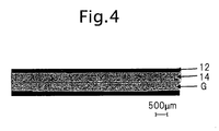
- FIG. 4 shows a photo of the cross-section including the growth axis from the graphite rod 12 through the seed crystal 14 to the single crystal growth layer G.
- An SiC single crystal grew by an extremely high degree of flatness on the SiC seed crystal. Note that the ratio of enlargement of diameter with respect to the seed crystal was about 1.2 times.
- FIG. 5(1) shows a photo of the cross-section including the growth axis from the graphite rod 12 through the seed crystal 14 to the single crystal growth layer G.
- An SiC single crystal grew by an extremely high degree of flatness on the SiC seed crystal.
- the SiC single crystal grown from the SiC seed crystal was increased in diameter by about two or more times. There were parts where the enlargement stopped due to polynucleated parts N occurring at part of the circumference, but these can be eliminated by considering the arrangement when first attaching the SiC seed crystal 14 to the graphite rod 12. Further, when further growing the crystal over this, it is confirmed that if removing the polynucleated parts N and then again growing the crystal, further enlargement of size occurs.
- An SiC seed crystal 14 with a growth surface made the (0001) plane was attached to the bottom end of a graphite rod 12, then inserted directly under the Si melt surface S to grow an SiC single crystal under the same growth conditions as Example 1.
- FIG. 6 shows a photo of the cross-section including the growth axis from the graphite rod 12 through the seed crystal 14 to the single crystal growth layer G. It will be understood that overall, flat growth is performed, but microsteps are formed and the mode of growth is affected sensitively by fluctuations in the growth conditions in the control range.
- FIG. 7 shows a photo of a growth surface of an SiC single crystal. Growth proceeds separately in the off angle direction whereby overall a large number of steps are formed and flat growth is not obtained at all.
- An SiC seed crystal 14 with a growth surface made the (11-20) plane (that is, with an off angle from the (0001) plane in the [11-20] direction of 90°) was attached to the bottom end of a graphite rod 12, then inserted directly under the Si melt surface S to grow an SiC single crystal under the same growth conditions as Example 1.
- FIGS. 8 (1) and (2) show (1) a photo of the cross-section including the growth axis from the graphite rod 12 through the seed crystal 14 to the single crystal growth layer G and (2) a photo of the growth surface of the SiC single crystal. Overall, the result was a large number of fine separate island shaped growth surfaces. Flat growth could not be obtained at all.
- a method of production of SiC single crystal using the solution method able to stably maintain flatness of a growth surface, prevent polycrystallization, and grow a large diameter SiC single crystal is provided.
Landscapes
- Chemical & Material Sciences (AREA)
- Engineering & Computer Science (AREA)
- Crystallography & Structural Chemistry (AREA)
- Materials Engineering (AREA)
- Metallurgy (AREA)
- Organic Chemistry (AREA)
- Inorganic Chemistry (AREA)
- Crystals, And After-Treatments Of Crystals (AREA)
Applications Claiming Priority (2)
| Application Number | Priority Date | Filing Date | Title |
|---|---|---|---|
| JP2006014726A JP2007197231A (ja) | 2006-01-24 | 2006-01-24 | SiC単結晶の製造方法 |
| PCT/JP2007/051109 WO2007094155A1 (ja) | 2006-01-24 | 2007-01-18 | SiC単結晶の製造方法 |
Publications (2)
| Publication Number | Publication Date |
|---|---|
| EP1978137A1 true EP1978137A1 (de) | 2008-10-08 |
| EP1978137A4 EP1978137A4 (de) | 2010-04-07 |
Family
ID=38371342
Family Applications (1)
| Application Number | Title | Priority Date | Filing Date |
|---|---|---|---|
| EP07707356A Withdrawn EP1978137A4 (de) | 2006-01-24 | 2007-01-18 | Verfahren zur herstellung von sic-einkristall |
Country Status (6)
| Country | Link |
|---|---|
| US (1) | US20090084309A1 (de) |
| EP (1) | EP1978137A4 (de) |
| JP (1) | JP2007197231A (de) |
| KR (1) | KR20080079332A (de) |
| CN (1) | CN101421442A (de) |
| WO (1) | WO2007094155A1 (de) |
Cited By (3)
| Publication number | Priority date | Publication date | Assignee | Title |
|---|---|---|---|---|
| WO2011101727A1 (en) * | 2010-02-18 | 2011-08-25 | Toyota Jidosha Kabushiki Kaisha | Method of producing silicon carbide single crystal |
| JP2012140267A (ja) * | 2010-12-28 | 2012-07-26 | Toyota Motor Corp | SiC単結晶の製造装置および製造方法 |
| EP3690085A4 (de) * | 2017-11-01 | 2021-07-07 | Central Glass Co., Ltd. | Verfahren zur herstellung eines siliciumcarbideinkristalls |
Families Citing this family (26)
| Publication number | Priority date | Publication date | Assignee | Title |
|---|---|---|---|---|
| JP4853449B2 (ja) * | 2007-10-11 | 2012-01-11 | 住友金属工業株式会社 | SiC単結晶の製造方法、SiC単結晶ウエハ及びSiC半導体デバイス |
| JP4998488B2 (ja) * | 2009-02-12 | 2012-08-15 | トヨタ自動車株式会社 | 溶液法によるSiC単結晶製造装置 |
| WO2010140564A1 (ja) * | 2009-06-01 | 2010-12-09 | 三菱化学株式会社 | 窒化物半導体結晶およびその製造方法 |
| CN102057083B (zh) * | 2009-07-21 | 2013-09-11 | 丰田自动车株式会社 | 使用熔液法的单晶生长用籽晶轴 |
| JP5439353B2 (ja) * | 2010-12-27 | 2014-03-12 | 新日鐵住金株式会社 | SiC単結晶の製造装置及びそれに用いられる坩堝 |
| JP5517913B2 (ja) * | 2010-12-27 | 2014-06-11 | 新日鐵住金株式会社 | SiC単結晶の製造装置、製造装置に用いられる治具、及びSiC単結晶の製造方法 |
| US9631295B2 (en) | 2011-03-23 | 2017-04-25 | Toyota Jidosha Kabushiki Kaisha | Method for producing SiC single crystals by control of an angle formed by the meniscus and the side face of the seed crystal and production device for the method |
| CN103608497B (zh) * | 2011-07-04 | 2016-10-12 | 丰田自动车株式会社 | SiC单晶及其制造方法 |
| JP5726035B2 (ja) * | 2011-09-28 | 2015-05-27 | 京セラ株式会社 | 結晶育成装置 |
| US10428440B2 (en) | 2012-04-20 | 2019-10-01 | Toyota Jidosha Kabushiki Kaisha | SiC single crystal and production method thereof |
| EP2876189B1 (de) * | 2012-07-19 | 2019-03-27 | Toyota Jidosha Kabushiki Kaisha | Vorrichtung zur herstellung eines silicium-einkristalls und verfahren zur herstellung eines silicium-einkristalls |
| JP5936191B2 (ja) * | 2012-08-26 | 2016-06-15 | 京セラ株式会社 | 結晶の製造方法 |
| WO2014034080A1 (ja) * | 2012-08-26 | 2014-03-06 | 国立大学法人名古屋大学 | 3C-SiC単結晶およびその製造方法 |
| EP2985369A4 (de) * | 2013-04-09 | 2016-12-21 | Nippon Steel & Sumitomo Metal Corp | Verfahren zur herstellung eines siliciumeinkristalls |
| JP6040866B2 (ja) * | 2013-05-29 | 2016-12-07 | トヨタ自動車株式会社 | SiC単結晶の製造方法 |
| JP6136772B2 (ja) * | 2013-08-30 | 2017-05-31 | 株式会社デンソー | 炭化珪素単結晶の製造方法 |
| JP5854013B2 (ja) | 2013-09-13 | 2016-02-09 | トヨタ自動車株式会社 | SiC単結晶の製造方法 |
| JP6060863B2 (ja) * | 2013-09-13 | 2017-01-18 | トヨタ自動車株式会社 | SiC単結晶及びその製造方法 |
| PL2881499T3 (pl) | 2013-12-06 | 2020-06-29 | Shin-Etsu Chemical Co., Ltd. | Sposób hodowli kryształu węgliku krzemu |
| JP6129065B2 (ja) * | 2013-12-06 | 2017-05-17 | 信越化学工業株式会社 | 炭化珪素の結晶成長方法 |
| JP6533716B2 (ja) | 2015-08-06 | 2019-06-19 | 信越化学工業株式会社 | SiC単結晶の製造方法 |
| JP2018080063A (ja) * | 2015-09-10 | 2018-05-24 | 新日鐵住金株式会社 | SiC単結晶の製造方法 |
| JP6784220B2 (ja) * | 2017-04-14 | 2020-11-11 | 信越化学工業株式会社 | SiC単結晶の製造方法 |
| JP7002932B2 (ja) * | 2017-12-22 | 2022-01-20 | 昭和電工株式会社 | SiCインゴットの製造方法 |
| CN108444284A (zh) * | 2018-03-14 | 2018-08-24 | 马鞍山市万兴耐磨金属制造有限公司 | 一种基于多级节能调控的中频熔炼电炉装置 |
| JP7164658B2 (ja) * | 2020-09-03 | 2022-11-01 | Ntn株式会社 | 窒化ケイ素焼結体、それを用いた転動体、および軸受 |
Family Cites Families (9)
| Publication number | Priority date | Publication date | Assignee | Title |
|---|---|---|---|---|
| JP2804860B2 (ja) * | 1991-04-18 | 1998-09-30 | 新日本製鐵株式会社 | SiC単結晶およびその成長方法 |
| JP4304783B2 (ja) * | 1999-09-06 | 2009-07-29 | 住友電気工業株式会社 | SiC単結晶およびその成長方法 |
| DE10247017B4 (de) * | 2001-10-12 | 2009-06-10 | Denso Corp., Kariya-shi | SiC-Einkristall, Verfahren zur Herstellung eines SiC-Einkristalls, SiC-Wafer mit einem Epitaxiefilm und Verfahren zur Herstellung eines SiC-Wafers, der einen Epitaxiefilm aufweist |
| JP3750622B2 (ja) * | 2002-03-22 | 2006-03-01 | 株式会社デンソー | エピタキシャル膜付きSiCウエハ及びその製造方法並びにSiC電子デバイス |
| JP4157326B2 (ja) * | 2002-05-27 | 2008-10-01 | 新日本製鐵株式会社 | 4h型炭化珪素単結晶インゴット及びウエハ |
| JP2004262709A (ja) * | 2003-02-28 | 2004-09-24 | Shikusuon:Kk | SiC単結晶の成長方法 |
| JP4593099B2 (ja) * | 2003-03-10 | 2010-12-08 | 学校法人関西学院 | 単結晶炭化ケイ素の液相エピタキシャル成長法及びそれに用いられる熱処理装置 |
| JP3764462B2 (ja) * | 2003-04-10 | 2006-04-05 | 株式会社豊田中央研究所 | 炭化ケイ素単結晶の製造方法 |
| JP4196791B2 (ja) * | 2003-09-08 | 2008-12-17 | トヨタ自動車株式会社 | SiC単結晶の製造方法 |
-
2006
- 2006-01-24 JP JP2006014726A patent/JP2007197231A/ja not_active Abandoned
-
2007
- 2007-01-18 EP EP07707356A patent/EP1978137A4/de not_active Withdrawn
- 2007-01-18 US US12/160,218 patent/US20090084309A1/en not_active Abandoned
- 2007-01-18 CN CNA2007800105995A patent/CN101421442A/zh active Pending
- 2007-01-18 WO PCT/JP2007/051109 patent/WO2007094155A1/ja not_active Ceased
- 2007-01-18 KR KR1020087018055A patent/KR20080079332A/ko not_active Ceased
Cited By (3)
| Publication number | Priority date | Publication date | Assignee | Title |
|---|---|---|---|---|
| WO2011101727A1 (en) * | 2010-02-18 | 2011-08-25 | Toyota Jidosha Kabushiki Kaisha | Method of producing silicon carbide single crystal |
| JP2012140267A (ja) * | 2010-12-28 | 2012-07-26 | Toyota Motor Corp | SiC単結晶の製造装置および製造方法 |
| EP3690085A4 (de) * | 2017-11-01 | 2021-07-07 | Central Glass Co., Ltd. | Verfahren zur herstellung eines siliciumcarbideinkristalls |
Also Published As
| Publication number | Publication date |
|---|---|
| WO2007094155A1 (ja) | 2007-08-23 |
| US20090084309A1 (en) | 2009-04-02 |
| EP1978137A4 (de) | 2010-04-07 |
| CN101421442A (zh) | 2009-04-29 |
| JP2007197231A (ja) | 2007-08-09 |
| KR20080079332A (ko) | 2008-08-29 |
Similar Documents
| Publication | Publication Date | Title |
|---|---|---|
| EP1978137A1 (de) | Verfahren zur herstellung von sic-einkristall | |
| JP4100228B2 (ja) | 炭化珪素単結晶とその製造方法 | |
| KR101310546B1 (ko) | 탄화규소 단결정의 제조 방법 | |
| KR101666596B1 (ko) | SiC 단결정 및 그 제조 방법 | |
| JP4853449B2 (ja) | SiC単結晶の製造方法、SiC単結晶ウエハ及びSiC半導体デバイス | |
| JP5562641B2 (ja) | マイクロパイプ・フリーの炭化ケイ素およびその製造方法 | |
| JP5273130B2 (ja) | SiC単結晶の製造方法 | |
| CN101910476B (zh) | 用于生长碳化硅单晶的方法 | |
| US7520930B2 (en) | Silicon carbide single crystal and a method for its production | |
| JP4561000B2 (ja) | 炭化珪素(SiC)単結晶の製造方法 | |
| US20120132130A1 (en) | METHOD OF PRODUCING SiC SINGLE CRYSTAL | |
| JP2007277049A (ja) | SiC単結晶の製造方法 | |
| JP4926556B2 (ja) | 炭化珪素単結晶インゴットの製造方法及び炭化珪素単結晶基板 | |
| KR101152857B1 (ko) | 탄화규소 단결정의 성장방법 | |
| JP5273131B2 (ja) | SiC単結晶の製造方法 | |
| WO2015137439A1 (ja) | SiC単結晶の製造方法 | |
| JP2014196242A (ja) | AlxGa1−xN結晶基板 | |
| JP6845418B2 (ja) | 炭化ケイ素単結晶ウェハ、インゴット及びその製造方法 | |
| JP5045232B2 (ja) | AlxGa1−xN結晶の成長方法 | |
| EP1498518B1 (de) | Verfahren zur herstellung eines siliciumcarbid-einkristalles | |
| JP4850663B2 (ja) | SiC単結晶の製造方法及びSiC単結晶基板の製造方法 | |
| JP2010275166A (ja) | 炭化珪素単結晶の製造方法 | |
| JP5777756B2 (ja) | β−Ga2O3系単結晶基板 | |
| JP4529712B2 (ja) | 化合物半導体単結晶の製造方法 | |
| WO2017043215A1 (ja) | SiC単結晶の製造方法 |
Legal Events
| Date | Code | Title | Description |
|---|---|---|---|
| PUAI | Public reference made under article 153(3) epc to a published international application that has entered the european phase |
Free format text: ORIGINAL CODE: 0009012 |
|
| 17P | Request for examination filed |
Effective date: 20080719 |
|
| AK | Designated contracting states |
Kind code of ref document: A1 Designated state(s): DE FR GB IT |
|
| DAX | Request for extension of the european patent (deleted) | ||
| RBV | Designated contracting states (corrected) |
Designated state(s): DE FR GB IT |
|
| A4 | Supplementary search report drawn up and despatched |
Effective date: 20100305 |
|
| STAA | Information on the status of an ep patent application or granted ep patent |
Free format text: STATUS: THE APPLICATION HAS BEEN WITHDRAWN |
|
| 18W | Application withdrawn |
Effective date: 20100615 |