EP1953589B1 - Liquid crystal display panel - Google Patents
Liquid crystal display panel Download PDFInfo
- Publication number
- EP1953589B1 EP1953589B1 EP08001779.1A EP08001779A EP1953589B1 EP 1953589 B1 EP1953589 B1 EP 1953589B1 EP 08001779 A EP08001779 A EP 08001779A EP 1953589 B1 EP1953589 B1 EP 1953589B1
- Authority
- EP
- European Patent Office
- Prior art keywords
- line
- liquid crystal
- electrode
- gate
- pattern
- Prior art date
- Legal status (The legal status is an assumption and is not a legal conclusion. Google has not performed a legal analysis and makes no representation as to the accuracy of the status listed.)
- Active
Links
- 239000004973 liquid crystal related substance Substances 0.000 title claims description 49
- 239000000758 substrate Substances 0.000 claims description 58
- 230000005684 electric field Effects 0.000 claims description 34
- 239000010410 layer Substances 0.000 description 27
- 239000011159 matrix material Substances 0.000 description 18
- 239000011241 protective layer Substances 0.000 description 7
- 238000009413 insulation Methods 0.000 description 5
- 239000004065 semiconductor Substances 0.000 description 5
- 239000003990 capacitor Substances 0.000 description 4
- 239000003086 colorant Substances 0.000 description 4
- 239000010949 copper Substances 0.000 description 4
- 239000010955 niobium Substances 0.000 description 4
- 239000011368 organic material Substances 0.000 description 4
- 239000004020 conductor Substances 0.000 description 3
- 238000009826 distribution Methods 0.000 description 3
- 238000005516 engineering process Methods 0.000 description 3
- 239000002356 single layer Substances 0.000 description 3
- VYZAMTAEIAYCRO-UHFFFAOYSA-N Chromium Chemical compound [Cr] VYZAMTAEIAYCRO-UHFFFAOYSA-N 0.000 description 2
- RYGMFSIKBFXOCR-UHFFFAOYSA-N Copper Chemical compound [Cu] RYGMFSIKBFXOCR-UHFFFAOYSA-N 0.000 description 2
- ZOKXTWBITQBERF-UHFFFAOYSA-N Molybdenum Chemical compound [Mo] ZOKXTWBITQBERF-UHFFFAOYSA-N 0.000 description 2
- VYPSYNLAJGMNEJ-UHFFFAOYSA-N Silicium dioxide Chemical compound O=[Si]=O VYPSYNLAJGMNEJ-UHFFFAOYSA-N 0.000 description 2
- BQCADISMDOOEFD-UHFFFAOYSA-N Silver Chemical compound [Ag] BQCADISMDOOEFD-UHFFFAOYSA-N 0.000 description 2
- 239000000956 alloy Substances 0.000 description 2
- 229910045601 alloy Inorganic materials 0.000 description 2
- 229910052782 aluminium Inorganic materials 0.000 description 2
- XAGFODPZIPBFFR-UHFFFAOYSA-N aluminium Chemical compound [Al] XAGFODPZIPBFFR-UHFFFAOYSA-N 0.000 description 2
- 229910021417 amorphous silicon Inorganic materials 0.000 description 2
- 230000000903 blocking effect Effects 0.000 description 2
- 229910052802 copper Inorganic materials 0.000 description 2
- 210000002858 crystal cell Anatomy 0.000 description 2
- 230000003247 decreasing effect Effects 0.000 description 2
- 229910010272 inorganic material Inorganic materials 0.000 description 2
- 239000011147 inorganic material Substances 0.000 description 2
- 238000004519 manufacturing process Methods 0.000 description 2
- 229910052751 metal Inorganic materials 0.000 description 2
- 239000002184 metal Substances 0.000 description 2
- 239000007769 metal material Substances 0.000 description 2
- 229910052750 molybdenum Inorganic materials 0.000 description 2
- 239000011733 molybdenum Substances 0.000 description 2
- 229910052758 niobium Inorganic materials 0.000 description 2
- GUCVJGMIXFAOAE-UHFFFAOYSA-N niobium atom Chemical compound [Nb] GUCVJGMIXFAOAE-UHFFFAOYSA-N 0.000 description 2
- 230000003287 optical effect Effects 0.000 description 2
- 230000002093 peripheral effect Effects 0.000 description 2
- 229910052814 silicon oxide Inorganic materials 0.000 description 2
- 229910052709 silver Inorganic materials 0.000 description 2
- 239000004332 silver Substances 0.000 description 2
- 239000010936 titanium Substances 0.000 description 2
- 239000004642 Polyimide Substances 0.000 description 1
- 229910052581 Si3N4 Inorganic materials 0.000 description 1
- 229910004205 SiNX Inorganic materials 0.000 description 1
- RTAQQCXQSZGOHL-UHFFFAOYSA-N Titanium Chemical compound [Ti] RTAQQCXQSZGOHL-UHFFFAOYSA-N 0.000 description 1
- NIXOWILDQLNWCW-UHFFFAOYSA-N acrylic acid group Chemical group C(C=C)(=O)O NIXOWILDQLNWCW-UHFFFAOYSA-N 0.000 description 1
- 239000000654 additive Substances 0.000 description 1
- 230000000996 additive effect Effects 0.000 description 1
- 230000005540 biological transmission Effects 0.000 description 1
- 239000013078 crystal Substances 0.000 description 1
- 230000007547 defect Effects 0.000 description 1
- 230000006866 deterioration Effects 0.000 description 1
- 230000009977 dual effect Effects 0.000 description 1
- 238000005530 etching Methods 0.000 description 1
- 239000011521 glass Substances 0.000 description 1
- AMGQUBHHOARCQH-UHFFFAOYSA-N indium;oxotin Chemical compound [In].[Sn]=O AMGQUBHHOARCQH-UHFFFAOYSA-N 0.000 description 1
- 230000001939 inductive effect Effects 0.000 description 1
- 230000002401 inhibitory effect Effects 0.000 description 1
- 239000011810 insulating material Substances 0.000 description 1
- 239000012212 insulator Substances 0.000 description 1
- 239000000203 mixture Substances 0.000 description 1
- 230000004048 modification Effects 0.000 description 1
- 238000012986 modification Methods 0.000 description 1
- 239000000049 pigment Substances 0.000 description 1
- 239000004033 plastic Substances 0.000 description 1
- 229920001721 polyimide Polymers 0.000 description 1
- HQVNEWCFYHHQES-UHFFFAOYSA-N silicon nitride Chemical compound N12[Si]34N5[Si]62N3[Si]51N64 HQVNEWCFYHHQES-UHFFFAOYSA-N 0.000 description 1
- 229910052719 titanium Inorganic materials 0.000 description 1
- WFKWXMTUELFFGS-UHFFFAOYSA-N tungsten Chemical compound [W] WFKWXMTUELFFGS-UHFFFAOYSA-N 0.000 description 1
- 229910052721 tungsten Inorganic materials 0.000 description 1
- 239000010937 tungsten Substances 0.000 description 1
- YVTHLONGBIQYBO-UHFFFAOYSA-N zinc indium(3+) oxygen(2-) Chemical compound [O--].[Zn++].[In+3] YVTHLONGBIQYBO-UHFFFAOYSA-N 0.000 description 1
Images

Classifications
-
- G—PHYSICS
- G02—OPTICS
- G02F—OPTICAL DEVICES OR ARRANGEMENTS FOR THE CONTROL OF LIGHT BY MODIFICATION OF THE OPTICAL PROPERTIES OF THE MEDIA OF THE ELEMENTS INVOLVED THEREIN; NON-LINEAR OPTICS; FREQUENCY-CHANGING OF LIGHT; OPTICAL LOGIC ELEMENTS; OPTICAL ANALOGUE/DIGITAL CONVERTERS
- G02F1/00—Devices or arrangements for the control of the intensity, colour, phase, polarisation or direction of light arriving from an independent light source, e.g. switching, gating or modulating; Non-linear optics
- G02F1/01—Devices or arrangements for the control of the intensity, colour, phase, polarisation or direction of light arriving from an independent light source, e.g. switching, gating or modulating; Non-linear optics for the control of the intensity, phase, polarisation or colour
- G02F1/13—Devices or arrangements for the control of the intensity, colour, phase, polarisation or direction of light arriving from an independent light source, e.g. switching, gating or modulating; Non-linear optics for the control of the intensity, phase, polarisation or colour based on liquid crystals, e.g. single liquid crystal display cells
- G02F1/133—Constructional arrangements; Operation of liquid crystal cells; Circuit arrangements
- G02F1/136—Liquid crystal cells structurally associated with a semi-conducting layer or substrate, e.g. cells forming part of an integrated circuit
- G02F1/1362—Active matrix addressed cells
- G02F1/136286—Wiring, e.g. gate line, drain line
-
- G—PHYSICS
- G02—OPTICS
- G02F—OPTICAL DEVICES OR ARRANGEMENTS FOR THE CONTROL OF LIGHT BY MODIFICATION OF THE OPTICAL PROPERTIES OF THE MEDIA OF THE ELEMENTS INVOLVED THEREIN; NON-LINEAR OPTICS; FREQUENCY-CHANGING OF LIGHT; OPTICAL LOGIC ELEMENTS; OPTICAL ANALOGUE/DIGITAL CONVERTERS
- G02F1/00—Devices or arrangements for the control of the intensity, colour, phase, polarisation or direction of light arriving from an independent light source, e.g. switching, gating or modulating; Non-linear optics
- G02F1/01—Devices or arrangements for the control of the intensity, colour, phase, polarisation or direction of light arriving from an independent light source, e.g. switching, gating or modulating; Non-linear optics for the control of the intensity, phase, polarisation or colour
- G02F1/13—Devices or arrangements for the control of the intensity, colour, phase, polarisation or direction of light arriving from an independent light source, e.g. switching, gating or modulating; Non-linear optics for the control of the intensity, phase, polarisation or colour based on liquid crystals, e.g. single liquid crystal display cells
- G02F1/133—Constructional arrangements; Operation of liquid crystal cells; Circuit arrangements
- G02F1/1333—Constructional arrangements; Manufacturing methods
- G02F1/1343—Electrodes
- G02F1/134309—Electrodes characterised by their geometrical arrangement
- G02F1/134318—Electrodes characterised by their geometrical arrangement having a patterned common electrode
-
- G—PHYSICS
- G02—OPTICS
- G02F—OPTICAL DEVICES OR ARRANGEMENTS FOR THE CONTROL OF LIGHT BY MODIFICATION OF THE OPTICAL PROPERTIES OF THE MEDIA OF THE ELEMENTS INVOLVED THEREIN; NON-LINEAR OPTICS; FREQUENCY-CHANGING OF LIGHT; OPTICAL LOGIC ELEMENTS; OPTICAL ANALOGUE/DIGITAL CONVERTERS
- G02F1/00—Devices or arrangements for the control of the intensity, colour, phase, polarisation or direction of light arriving from an independent light source, e.g. switching, gating or modulating; Non-linear optics
- G02F1/01—Devices or arrangements for the control of the intensity, colour, phase, polarisation or direction of light arriving from an independent light source, e.g. switching, gating or modulating; Non-linear optics for the control of the intensity, phase, polarisation or colour
- G02F1/13—Devices or arrangements for the control of the intensity, colour, phase, polarisation or direction of light arriving from an independent light source, e.g. switching, gating or modulating; Non-linear optics for the control of the intensity, phase, polarisation or colour based on liquid crystals, e.g. single liquid crystal display cells
- G02F1/133—Constructional arrangements; Operation of liquid crystal cells; Circuit arrangements
- G02F1/136—Liquid crystal cells structurally associated with a semi-conducting layer or substrate, e.g. cells forming part of an integrated circuit
- G02F1/1362—Active matrix addressed cells
- G02F1/136218—Shield electrodes
-
- G—PHYSICS
- G02—OPTICS
- G02F—OPTICAL DEVICES OR ARRANGEMENTS FOR THE CONTROL OF LIGHT BY MODIFICATION OF THE OPTICAL PROPERTIES OF THE MEDIA OF THE ELEMENTS INVOLVED THEREIN; NON-LINEAR OPTICS; FREQUENCY-CHANGING OF LIGHT; OPTICAL LOGIC ELEMENTS; OPTICAL ANALOGUE/DIGITAL CONVERTERS
- G02F2201/00—Constructional arrangements not provided for in groups G02F1/00 - G02F7/00
- G02F2201/12—Constructional arrangements not provided for in groups G02F1/00 - G02F7/00 electrode
- G02F2201/121—Constructional arrangements not provided for in groups G02F1/00 - G02F7/00 electrode common or background
-
- G—PHYSICS
- G02—OPTICS
- G02F—OPTICAL DEVICES OR ARRANGEMENTS FOR THE CONTROL OF LIGHT BY MODIFICATION OF THE OPTICAL PROPERTIES OF THE MEDIA OF THE ELEMENTS INVOLVED THEREIN; NON-LINEAR OPTICS; FREQUENCY-CHANGING OF LIGHT; OPTICAL LOGIC ELEMENTS; OPTICAL ANALOGUE/DIGITAL CONVERTERS
- G02F2201/00—Constructional arrangements not provided for in groups G02F1/00 - G02F7/00
- G02F2201/12—Constructional arrangements not provided for in groups G02F1/00 - G02F7/00 electrode
- G02F2201/122—Constructional arrangements not provided for in groups G02F1/00 - G02F7/00 electrode having a particular pattern
Definitions
- the present disclosure of invention relates to a liquid crystal display (“LCD”) panel and, in particular, to an improved LCD panel which is capable of inhibiting light leakage around gate lines when using a liquid crystal alignment distribution mode that is intended to provide enhanced side view visibility and to also provide high transmissivity for improving apparent contrast ratio.
- LCD liquid crystal display
- An LCD device displays a desired image by supplying a video signal to liquid crystal cells arranged in a matrix form and by controlling light transmissivity of the individual liquid crystal cells according to pixel drive signals embedded in the video signal.
- Optical viewing angle technologies have been developed to solve a viewing angle problem inherent to LCDs wherein appearance of a displayed image might be distorted according to a location from which a viewer watches a screen where the location may be one other than that of a heads on direct facing view of the screen.
- the optical viewing angle improving technologies used for LCD devices include a so-called, Patterned-ITO Vertical Alignment ("PVA”) mode, an In-Plane Switching (“IPS”) mode, and a Plane-to-Line Switching (“PLS”) mode.
- PVA Patterned-ITO Vertical Alignment
- IPS In-Plane Switching
- PLS Plane-to-Line Switching
- a fringe electric field is generated between a common electrode and a pixel electrode formed respectively in first and second base substrates due to provision of slits in the electrodes.
- Liquid crystal molecules are symmetrically driven into different orientations on the basis of the placement of the slits and the distributed fringe electric fields generated around the locals of the slits, thereby forming a multi-domain distribution of crystal orientations.
- the liquid crystal molecules are oriented by a lateral electric field formed between a common electrode and a pixel electrode where the latter are both formed to be parallel to each other on a second base substrate.
- an insulator is disposed between the common electrode and the pixel electrode in each pixel area.
- liquid crystal molecules are both laterally and vertically aligned with respect to a shaped electric field generated by specially shaped electrode patterns formed on first and second side transparent substrates of the LCD panel.
- One embodiment of the DFS mode uses a common electrode and a pixel electrode linearly formed in respective planes on the first and second base substrates.
- the liquid crystal molecules are aligned using a liquid crystal driving electric field in which a lateral (horizontal) portion of the electric field and a vertical portion of the electric field are generated between the common electrode and the pixel electrode in a mixed distributive manner, thereby improving side view visibility and also improving light transmissivity (by keeping the per pixel aperture ratio relatively large).
- the liquid crystal molecules are driven by electrodes formed over the whole pixel unit area, the transmission area is wide and thus provides good transmissivity.
- the liquid crystal molecules are easily moved by the influence of electric fields from adjacent electrodes (in particular those from adjacent gate lines) and thus it is difficult to prevent extraneous orientations of liquid crystal molecules from being formed about peripheral regions of the different pixel areas.
- An LCD panel using a conventional form of the proposed DFS mode suffers from a relatively low contrast ratio when displaying a black or dark gray level since light leakage tends to occur in the vicinity of gate lines due to extraneous orientations of liquid crystal molecules around the gate lines.
- the irregularly arranged liquid crystal molecules in the area of gate lines are not capable of properly suppressing light transmissivity when a black or dark gray level is desired in the adjoining pixel area, and they thereby can generate light leakage and decrease the apparent contrast ratio of the black or dark gray level in the adjoining pixel area in certain situations so as to give users of the DFS operated panel the impression that the adjoining pixel area is not as dark as it should be.
- the LCD panel of the DFS mode uses a black matrix in the vicinity of the gate lines for the purpose of blocking light leakage around peripheral edges of each pixel area
- the black matrix has a tendency to deviate during mass production from its design-specified normal location due to an arrangement (alignment) error of the first and second base substrates when assembling the LCD panel on a mass production basis.
- the so-misaligned black matrix is incapable of blocking all the light leakage generated by the liquid crystal molecules adjacent to the gate lines and thus the contrast ratio of the black or dark gray level is disadvantageously decreased when misalignment of the black matrix occurs.
- the present disclosure of invention provides an LCD panel which includes means for shielding against extraneous electric fields being generated in the vicinity of the gate line segments that adjoin darkened pixel areas and it thus prevents extraneous orientations of liquid crystal molecules in the vicinity of the gate line segments from occurring and it thus reduces the corresponding light leakage that tends to occur around the vicinity of the gate lines, this thereby improving the apparent contrast ratio for darkened pixels of the LCD panel.
- the LCD panel of the present invention includes a first base substrate, a plurality of gate lines and a plurality of data lines disposed on the first base substrate and crossing each other, a pixel electrode comprising a first oblique line and a second oblique line disposed on the first base substrate and inclined in a different direction from each other with respect to the gate lines, a second base substrate, a common electrode disposed on the second base substrate and alternately positioned with the pixel electrode, wherein a portion of the common electrode overlaps the gate line segment; and a liquid crystal layer disposed between the first and second base substrates.
- the pixel electrode is formed to have spaced apart first stripes with a prescribed spacing distance and wherein the common electrode is formed to have spaced apart second stripes with the same spacing distance.
- a portion of the common electrode overlaps a gate electrode.
- the LCD panel according to the invention includes a first base substrate, a plurality of gate lines and a plurality of data lines disposed on the first base substrate and crossing each other, a pixel electrode comprising a first oblique line and a second oblique line disposed on the first base substrate and inclined in a different direction from each other with respect to the gate lines, a second base substrate, a common electrode disposed on the second base substrate,wherein the common electrode comprises, a first pattern line formed to be parallel with the data line, a second pattern line alternating with corresponding pattern lines of the pixel electrode according to a prescribed distance to form a liquid crystal driving electric field together with the pixel electrode and a third pattern line overlapping the gate line segment and a liquid crystal layer disposed between the first and second base substrates.
- the third pattern line is formed with a substantially larger width than a width of the underlying gate line segment.
- the second pattern line is obliquely formed to correspond to the pixel electrode.
- the common electrode includes a slit formed in the third pattern line on the gate line.
- the slit is formed on the gate line to be parallel with the gate line.
- the slit divides the third pattern line overlapping the gate line into at least two parts.
- the portion of common electrode overlaps the gate electrode.
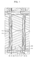
- FIG. 1 is a plan view illustrating an LCD panel according to the invention.
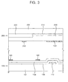
- FIG. 2 and FIG. 3 are cross-sectional views taken along line I-I' and line II-II' of FIG. 1 , respectively.
- the LCD panel includes a TFT substrate 100, a color filter substrate 200 affixed in spaced apart facing relation to the TFT substrate 100, and liquid crystals interposed between the TFT substrate 100 and the color filter substrate 200.
- the TFT substrate 100 includes a gate line 110 and a data line 140 formed on a first base substrate 101, and a pixel electrode 160 formed as linear stripes in a corresponding pixel area, where the corresponding pixel area is bounded by the gate line 110 and the data line 140.
- the color filter substrate 200 includes a common electrode 240 designed to form shaped first electric fields together with the pixel electrode 160.
- the common electrode 240 is formed as linear stripes that are staggered to alternate with the stripes of the pixel electrode 160 according to a prescribed staggering distance and to also generously overlap with the gate line 110.
- the liquid crystals are driven into corresponding orientations by the electric fields generated by a difference of a data voltage supplied to the pixel electrode 160 of TFT substrate 100 and of a common voltage supplied to the common electrode 240 of the color filter substrate 200.
- the supplied data voltage thus controls the transmissivity of light supplied from a light source through the corresponding pixel area.
- the liquid crystals are normally horizontally aligned and provided with positive dielectric anisotropy.
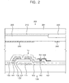
- the TFT substrate 100 includes the gate line 110 and the date line 140 formed on the first base substrate 101 by crossing each other, a TFT denoted as T1 and formed in a corner of the pixel area, where the pixel electrode 160 connects to the TFT T1.
- a protective layer 150 covers the TFT T1 to insulate the TFT T1 from other electrodes.
- a storage line 115 may be formed to run parallel with the gate line 110 and to connect to a storage electrode 116 that forms a charge storage capacitor. As understood by artisans skilled in the art, the storage capacitor augments an LCD capacitor defined by the pixel-electrode, the overlapping portion of the common electrode and the liquid crystal dielectric therebetween.
- the first base substrate 101 portion of the TFT substrate is made of a transparent insulating material such as glass or plastic.
- the gate line 110 is transversely formed on the first base substrate 101.
- the gate line 110 is formed of a single layer or a plurality of conductor layers including one of molybdenum (“Mo”), niobium (“Nb”), copper (“Cu”), aluminum (“Al”), chrome (“Cr”), silver (“Ag”), tungsten (“W”), or an alloy thereof.
- Mo molybdenum
- Nb niobium
- Cu copper
- Al aluminum
- Cr chrome
- silver Ag
- W tungsten
- a gate electrode 111 is formed in a crossing area of the gate line 110 and the data line 140.
- the data line 140 is vertically formed on the first base substrate 101.
- the data line 140 is formed of a single layer or a plurality of conductor layers including one of molybdenum (“Mo”), niobium (“Nb”), copper (“Cu”), aluminum (“Al”), chrome (“Cr”), silver (“Ag”), titanium (“Ti”), or an alloy thereof.
- Mo molybdenum
- Nb niobium
- Cu copper
- Al aluminum
- Cr chrome
- silver Ag
- Ti titanium
- a source electrode 141 and a drain electrode 143 are formed in a crossing area of the gate line 110 and the data line 140.
- the TFT T1 includes the gate electrode 111, a gate insulation layer 120 which insulates the gate electrode 111 from a semiconductor layer 130, the semiconductor layer 130 formed on the gate insulation layer 120, and source and drain electrodes 141 and 143 spaced apart from each other on the semiconductor layer 130.
- the gate electrode 111 protrudes from the one side of the gate line 110 and controls a driving of the TFT T1 through a gate driving signal supplied from the gate line 110. During a horizontal scan period, the gate driving signal drives the TFT to be turned on so as to charge its pixel-electrode towards a desired data voltage.
- the gate insulation layer 120 covers the gate electrode 111 to insulate the gate electrode 111 made of a conductive metal material from other electrodes made of other metal materials.
- the semiconductor layer 130 includes an active layer 131 made for example of amorphous silicon and an ohmic contact layer 132 made for example of heavily doped (e.g., N+) amorphous silicon.
- the source electrode 141 is formed in, but not limited to, a "U" shape so as to surround the drain electrode 143 but remain spaced apart from the drain electrode 143 with a prescribed distance (a channel length).
- the source electrode 141 may be formed in various shapes.
- One side of the drain electrode 143 is formed to face the source electrode 141 and the other side thereof is formed with a wider area to be connected to the pixel electrode 160 of the corresponding pixel area.
- the drain electrode 143 may be formed in various shapes.
- the source electrode 141 receives a data signal from the data line 140 where the data signal defines a light transmissivity that is to be attained by the pixel area in order to display a corresponding image.
- the drain electrode 143 receives a passed-through data voltage as passed from the source electrode 141 through the channel region of the semiconductor layer 130 when the TFT is turned on. The data voltage supplied to the drain electrode 143 is further transferred to the pixel electrode 160 connected to the other side of the drain electrode 143.
- the protective layer 150 is formed of an inorganic material such as a silicon nitride ("SiNx”) or a silicon oxide (“SiOx”), or an organic material such as acrylic, polyimide or benzoclylobutene (“BCB”).
- the protective layer 150 is formed as a single layer or multiple layers staked by the inorganic material and the organic material.
- the protective layer 150 covers the TFT T1 and the gate insulation layer 120 to insulate the TFT T1 from other electrodes such as the pixel electrode 160.
- the protective layer 150 includes a contact hole 151 exposing a part of the drain electrode 143 for contact with the pixel-electrode 160.
- the contact hole 151 may be formed by etching a part of the protective layer 150 covering the drain electrode 143 using a mask.
- the pixel electrode 160 is formed on the protective layer 150 and connected to the drain electrode 143 of the TFT T1 through the contact hole 151.
- the pixel electrode 160 is linearly formed in the pixel area with a prescribed width.
- the pixel electrode 160 includes vertical lines, horizontal lines and oblique lines.
- the horizontal lines and vertical lines of the pixel-electrode respectively overlap the storage line 115 and the storage electrode 116 to form the storage capacitor.
- the oblique lines of the pixel-electrode connect the vertical lines to each other and are spaced apart with a prescribed spacing distance to define a symmetric pattern about a horizontal line located at the center of the pixel area and coaxial with the storage line 115.
- the oblique lines are inclined with respect to the long or short sides of the first base substrate 101.
- a first liquid crystals alignment layer (not shown) is formed on the top surface of the TFT substrate 100 including the pixel electrode 160.
- a horizontal alignment layer is formed on the TFT substrate 100.
- a rubbing direction of the alignment layer is parallel with the long or short side of the first base substrate 101.
- the oblique lines of the pixel electrode 160 are at a prescribed angle with respect to the rubbing direction of the alignment layer. In one embodiment, the prescribed angle is about 10° to about 30°.
- the color filter substrate 200 includes the black matrix 210 on a second base substrate 201 to help prevent light leakage.
- the color filter substrate 200 also includes the color filter 220 to display colors, an overcoat layer 230 to reduce the stepped height or to improve planarity between the black matrix 210 and the color filter 220, and the common electrode 240 to supply the common voltage to the liquid crystal.
- the black matrix 210 is formed so that it vertically overlaps the TFT T1 , the gate line 110, the data line 140, and the storage line 115 of the TFT substrate 100 in order to prevent light from leaking.
- the black matrix 210 may be formed of an opaque organic material or metal.
- the color filter 220 is formed under the black matrix 210 and includes red (“R”), green (“G”), and color blue (“B”) color filters to display colors.
- the color filter 220 absorbs or transmits light of a specific wavelength for example through R, G, and B pigments, thereby displaying R, G, and B colors.
- the LCD panel can display the various colors by additive mixture of the transmitted R, G, and B lights.
- the overcoat layer 230 is formed of a transparent organic material to protect the color filter 220 and the black matrix 210.
- the overcoat layer 230 is formed for good step coverage and insulation of the common electrode 240.
- the common electrode 240 is formed of a transparent conductor (e.g., a metal) such as indium tin oxide ("ITO") or indium zinc oxide (“IZO").
- the common electrode 240 receives the common voltage, i.e. a reference voltage.
- the shape of the common electrode 240 contributes to defining electric fields generated through the liquid crystal layer due to the differences for example between the common voltage and the data voltage of the pixel electrode 160.
- the common electrode 240 is arranged to include a symmetrical set of oblique stripes inclined toward the long or short side of the second base substrate 201.
- a second alignment layer (not shown) is formed on a lowest surface of the color filter substrate 200 including the common electrode 240.
- a second horizontal alignment layer is formed on the color filter substrate 200.
- a rubbing direction of the second alignment layer like the rubbing direction of the TFT substrate 100, is parallel with the long or short side of the second base substrate 201.
- the common electrode 240 is at a prescribed angle with respect to the rubbing direction of the alignment layer. In one embodiment, the prescribed angle is about 10° to about 30.
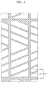
- FIG. 4 is a plan view illustrating the common electrode shown in FIG. 1 according to one exemplary embodiment of the present invention.
- the common electrode 240 includes a first pattern line 241, a second pattern line 242, and a third pattern line 243.
- the first pattern line 241 extends vertically to overlap the data line 140 in the TFT substrate below.
- the second pattern line 242 is obliquely formed relative to the first pattern line 241 and extended linearly to become connected to two parallel and successive ones of the first pattern lines 241.
- the second pattern lines 242 are formed to run parallel with the oblique lines of the pixel electrode 160 with the same spacing distance being present between successive ones of the second pattern lines 242 as is present between successive ones of the oblique lines of the pixel electrode 160.
- the second pattern lines 242 are staggered relative to the oblique lines of the pixel electrodes 160 so as to maintain a same staggering distance between oblique lines of the TFT substrate and oblique lines of the color filters substrate. An example of the staggering is seen for example in Fig.
- the third pattern line 243 is transversely formed to generously overlap with the underlying gate line segment 110 as may be seen for example in Fig. 3 .
- a common voltage is supplied to the third pattern line 243.
- an electric field is formed between the third pattern line 243 and the underlying gate line segment 110 where the formed electric field is different from the fringe fields formed between the staggered oblique lines.
- the third pattern line 243 is shaped to prevent an extraneous liquid crystal orientation influence that can be exerted by its electric field alone so that the liquid crystal molecules affected by the liquid crystal driving electric field generated between the oblique line of the adjacent pixel electrode 160 and the adjacent second pattern line 242 may continue to be substantially similarly regularly arranged as one moves from the vicinity of the second pattern lines 242 towards the region where the third pattern line 243 overlaps the gate line segment 110.
- the third pattern line 243 may formed above the gate line segment 110 with a substantially larger width than the gate line segment 110.
- the third pattern line 243 works to prevent extraneous light leakage around the region of the gate line segment 110 by forming an electric field to the underlying gate line segment 110 where the formed third-line to gate-line field is at least partially intermixed with and thus controlled by the liquid crystal driving electric field formed between the pixel electrode 160 and the adjacent second pattern line 242.
- the third pattern line 243 of the common electrode 240 operates to prevent light leakage from getting around a misaligned black matrix 210 by intentionally inducing cross talk between the electric fields of the pixel-electrode lines 160 and the electric field of the gate line segment 110.
- the LCD panel drives the liquid crystal to display a black or dark gray level in the pixel area of the adjacent pixel-electrode
- the liquid crystals in the vicinity of the gate line segment 110 are influenced by this pixel darkening drive to be irregularly arranged due to the influence of the fringe electric fields generated between the substantially wide third pattern line 243 and the adjacent lines of the pixel-electrode even while the gate line segment 110 is receiving a substantially different voltage (e.g., a gate turn on voltage) from the black or dark gray level voltage stored on the adjacent pixel-electrode 160.
- a substantially different voltage e.g., a gate turn on voltage
- the black matrix 210 should prevent leakage of light transmitted through these irregularly arranged liquid crystals around the vicinity of the gate line segment 110 irrespective of the current voltage on the gate line 110.
- the black matrix 210 when the black matrix 210 is misaligned by a relatively large margin due to misalignments during assembly, the black matrix by itself may fail to block the light that is influenced only by the voltage on the gate line 110.
- the electric fields formed about the gate line 110 are not free of influence from the black or dark gray causing fields formed between the wide third pattern line 243 and the nearest oblique line 160 of the pixel-electrode.
- the LCD panel has less of a decrease in contrast ratio of the black or dark gray levels than seen due to light leakage in panels that do not have such an arrangement of a relatively narrow gate line 110 and a substantially wider common electrode portion 243 overlying that relatively narrow gate line 110. Due to the intentionally created cross talk between the electric fields, the liquid crystals in the vicinity of the gate line 110 are partially controlled by the intermixing of the electric field generated between the pixel electrode 160 and the second pattern line 242. Therefore, the extra wide third portion 243 of the common electrode 240 works to suppress light leakage which is not otherwise blocked by the black matrix 210.
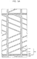
- FIG. 5A and FIG. 5B are respectively a plan view and a cross-sectional view illustrating a common electrode according to the invention.
- the common electrode 240 of Figs. 5A-5B includes a slit 244 in third portion 243.
- the slit 244 is formed centrally above the gate line 110 so that the third portion 243 still generously overlaps the gate line 110 and where the slit 244 divides the third pattern line 243 into adjacent sublines 245 and 246.
- the common electrode 240 includes a first pattern line 241 extending in the vertical direction, a second oblique pattern line 242 and a third horizontal pattern line 243.
- the detailed descriptions of the first pattern line 241 and the second pattern line 242 will be omitted here since these are substantially the same as the in the first exemplary embodiment of Fig. 4 .
- the third pattern line 243 is transversely formed to generously overlap the gate line 110.
- the third pattern line 243 is divided into two or more parts by for example the illustrated first slit 244.
- the third pattern line 243 is formed to be divided into a first subline 245 and a second subline 246 by the slit 244.
- the slit 244 is formed in the third pattern line 243 with a prescribed length and width such as shown in Fig. 5A for example.
- the first subline 245 and the second subline 246 operate to suppress the influence of the electric field generated only be the narrower gate line 110.
- the combination of the first subline 245 and the second subline 246 is sufficiently wide so as to create a substantial amount of crosstalk so that the field between pixel electrode 160 and the second pattern line 242 mixes in with the field of the gate line 110 and thus partially controls the orientation of the liquid crystal molecules around the vicinity of the gate line 110. Therefore, the wide configuration of the first subline 245 and the second subline 246 operate to suppress light leakage which might otherwise occur due to misalignment of the black matrix 210 caused by an assembly defect.
- an LCD panel in accordance with the disclosure includes a generously wide common electrode portion (243) that overlaps with a substantially narrower gate line and which is distanced from the nearest oblique line of the pixel-electrode so as to form an electric field together with the gate line that is crosstalk wise influenced by the field (e.g., black or dark gray luminosity field) of the adjacent pixel-electrode and is thus suppressed from generating stray light when the adjacent pixel-electrode is in a black or dark gray luminosity mode.
- the field e.g., black or dark gray luminosity field
- the liquid crystal display panel operates to suppress light leakage around the gate line by controlling the fields that might cause irregularly arranged distributions of liquid crystal around the gate line. Therefore, the so-configured LCD panel helps to reduce deterioration of contrast ratio when the black mask is misaligned.
Applications Claiming Priority (1)
| Application Number | Priority Date | Filing Date | Title |
|---|---|---|---|
| KR1020070010562A KR101427708B1 (ko) | 2007-02-01 | 2007-02-01 | 액정 표시 패널 |
Publications (3)
| Publication Number | Publication Date |
|---|---|
| EP1953589A2 EP1953589A2 (en) | 2008-08-06 |
| EP1953589A3 EP1953589A3 (en) | 2010-06-02 |
| EP1953589B1 true EP1953589B1 (en) | 2014-04-23 |
Family
ID=39301785
Family Applications (1)
| Application Number | Title | Priority Date | Filing Date |
|---|---|---|---|
| EP08001779.1A Active EP1953589B1 (en) | 2007-02-01 | 2008-01-31 | Liquid crystal display panel |
Country Status (5)
| Country | Link |
|---|---|
| US (1) | US8610863B2 (ja) |
| EP (1) | EP1953589B1 (ja) |
| JP (1) | JP5475955B2 (ja) |
| KR (1) | KR101427708B1 (ja) |
| CN (1) | CN101236339B (ja) |
Families Citing this family (80)
| Publication number | Priority date | Publication date | Assignee | Title |
|---|---|---|---|---|
| KR101413275B1 (ko) * | 2007-01-29 | 2014-06-30 | 삼성디스플레이 주식회사 | 액정 표시 패널 및 이의 제조 방법 |
| JP4693131B2 (ja) | 2008-02-14 | 2011-06-01 | 東芝モバイルディスプレイ株式会社 | 液晶表示装置 |
| JP5035931B2 (ja) | 2010-03-29 | 2012-09-26 | 株式会社ジャパンディスプレイセントラル | 液晶表示装置 |
| JP5380416B2 (ja) | 2010-10-20 | 2014-01-08 | 株式会社ジャパンディスプレイ | 液晶表示装置 |
| JP5597557B2 (ja) * | 2011-01-13 | 2014-10-01 | 株式会社ジャパンディスプレイ | 液晶表示装置 |
| JP5572562B2 (ja) | 2011-01-19 | 2014-08-13 | 株式会社ジャパンディスプレイ | 液晶表示装置 |
| JP5695946B2 (ja) | 2011-03-17 | 2015-04-08 | 株式会社ジャパンディスプレイ | 液晶表示装置 |
| JP5377555B2 (ja) | 2011-03-29 | 2013-12-25 | 株式会社ジャパンディスプレイ | 液晶表示装置 |
| JP5552457B2 (ja) | 2011-03-31 | 2014-07-16 | 株式会社ジャパンディスプレイ | 液晶表示装置 |
| KR20140133963A (ko) | 2011-04-08 | 2014-11-20 | 가부시키가이샤 재팬 디스프레이 | 액정 표시 장치 |
| KR101635668B1 (ko) | 2011-04-08 | 2016-07-01 | 가부시키가이샤 재팬 디스프레이 | 액정 표시 장치 |
| JP5530971B2 (ja) | 2011-04-19 | 2014-06-25 | 株式会社ジャパンディスプレイ | 液晶表示装置 |
| JP5616841B2 (ja) | 2011-04-22 | 2014-10-29 | 株式会社ジャパンディスプレイ | 液晶表示装置 |
| JP5377567B2 (ja) | 2011-04-25 | 2013-12-25 | 株式会社ジャパンディスプレイ | 液晶表示装置 |
| JP5504215B2 (ja) | 2011-07-08 | 2014-05-28 | 株式会社ジャパンディスプレイ | 液晶表示装置 |
| JP5759813B2 (ja) | 2011-07-13 | 2015-08-05 | 株式会社ジャパンディスプレイ | 液晶表示装置 |
| JP5386555B2 (ja) | 2011-07-28 | 2014-01-15 | 株式会社ジャパンディスプレイ | 液晶表示装置 |
| JP5564473B2 (ja) | 2011-08-05 | 2014-07-30 | 株式会社ジャパンディスプレイ | 液晶表示装置 |
| JP5674587B2 (ja) | 2011-08-05 | 2015-02-25 | 株式会社ジャパンディスプレイ | 液晶表示装置 |
| JP5520896B2 (ja) | 2011-08-08 | 2014-06-11 | 株式会社ジャパンディスプレイ | 液晶表示装置 |
| JP5530987B2 (ja) | 2011-08-09 | 2014-06-25 | 株式会社ジャパンディスプレイ | 液晶表示装置 |
| JP5520897B2 (ja) | 2011-08-11 | 2014-06-11 | 株式会社ジャパンディスプレイ | 液晶表示装置 |
| JP5707273B2 (ja) | 2011-08-12 | 2015-04-22 | 株式会社ジャパンディスプレイ | 液晶表示装置 |
| JP5520899B2 (ja) | 2011-08-23 | 2014-06-11 | 株式会社ジャパンディスプレイ | 液晶表示装置 |
| JP5577308B2 (ja) | 2011-08-25 | 2014-08-20 | 株式会社ジャパンディスプレイ | 液晶表示装置 |
| JP5663436B2 (ja) * | 2011-08-26 | 2015-02-04 | 株式会社ジャパンディスプレイ | 液晶表示装置 |
| JP5572603B2 (ja) * | 2011-08-30 | 2014-08-13 | 株式会社ジャパンディスプレイ | 液晶表示装置 |
| JP5677239B2 (ja) | 2011-08-31 | 2015-02-25 | 株式会社ジャパンディスプレイ | 液晶表示装置および液晶表示装置の製造方法 |
| JP5906043B2 (ja) | 2011-09-01 | 2016-04-20 | 株式会社ジャパンディスプレイ | 液晶表示装置 |
| JP5560247B2 (ja) | 2011-09-02 | 2014-07-23 | 株式会社ジャパンディスプレイ | 液晶表示装置 |
| US9075271B2 (en) | 2011-09-06 | 2015-07-07 | Japan Display Inc. | Liquid crystal display device |
| US9250486B2 (en) | 2011-09-08 | 2016-02-02 | Japan Display Inc. | Liquid crystal display device |
| JP5785831B2 (ja) | 2011-09-12 | 2015-09-30 | 株式会社ジャパンディスプレイ | 液晶表示装置 |
| JP5926523B2 (ja) | 2011-09-16 | 2016-05-25 | 株式会社ジャパンディスプレイ | 液晶表示装置 |
| US8786534B2 (en) | 2011-09-27 | 2014-07-22 | Japan Display Inc. | Liquid crystal display device |
| JP5677923B2 (ja) | 2011-09-28 | 2015-02-25 | 株式会社ジャパンディスプレイ | 液晶表示装置 |
| JP5845035B2 (ja) | 2011-09-28 | 2016-01-20 | 株式会社ジャパンディスプレイ | 液晶表示装置 |
| JP5740278B2 (ja) | 2011-10-11 | 2015-06-24 | 株式会社ジャパンディスプレイ | 液晶表示装置 |
| US9019439B2 (en) | 2011-10-14 | 2015-04-28 | Japan Display Inc. | Liquid crystal display device |
| JP5771501B2 (ja) | 2011-10-17 | 2015-09-02 | 株式会社ジャパンディスプレイ | 液晶表示装置 |
| JP5759871B2 (ja) | 2011-11-08 | 2015-08-05 | 株式会社ジャパンディスプレイ | 液晶表示装置 |
| JP6104548B2 (ja) | 2011-11-08 | 2017-03-29 | 株式会社ジャパンディスプレイ | 液晶表示装置 |
| JP5699069B2 (ja) | 2011-11-21 | 2015-04-08 | 株式会社ジャパンディスプレイ | 液晶表示装置 |
| CN102436088B (zh) * | 2011-12-14 | 2015-03-25 | 深圳市华星光电技术有限公司 | 液晶显示装置 |
| US8873007B2 (en) * | 2011-12-14 | 2014-10-28 | Shenzhen China Star Optoelectronics Technology Co., Ltd. | Liquid crystal display device |
| US9052555B2 (en) | 2011-12-28 | 2015-06-09 | Japan Display Inc. | Liquid crystal display device |
| JP5750074B2 (ja) * | 2012-03-12 | 2015-07-15 | 株式会社ジャパンディスプレイ | 液晶表示装置、液晶表示装置の製造方法、および電子機器 |
| JP2013190662A (ja) | 2012-03-14 | 2013-09-26 | Japan Display Inc | 液晶表示装置 |
| JP2013195686A (ja) | 2012-03-19 | 2013-09-30 | Japan Display Inc | 液晶表示装置 |
| JP5903309B2 (ja) | 2012-03-28 | 2016-04-13 | 株式会社ジャパンディスプレイ | 液晶表示装置 |
| JP6039914B2 (ja) | 2012-04-06 | 2016-12-07 | 株式会社ジャパンディスプレイ | 液晶表示装置 |
| JP6010330B2 (ja) | 2012-04-23 | 2016-10-19 | 株式会社ジャパンディスプレイ | 液晶表示装置 |
| JP5926608B2 (ja) | 2012-05-08 | 2016-05-25 | 株式会社ジャパンディスプレイ | 液晶表示装置及びその製造方法 |
| JP5883721B2 (ja) | 2012-05-11 | 2016-03-15 | 株式会社ジャパンディスプレイ | 液晶表示装置 |
| JP5978001B2 (ja) | 2012-05-22 | 2016-08-24 | 株式会社ジャパンディスプレイ | 液晶表示装置 |
| JP5953120B2 (ja) | 2012-05-25 | 2016-07-20 | 株式会社ジャパンディスプレイ | 液晶表示装置 |
| JP5906138B2 (ja) | 2012-05-29 | 2016-04-20 | 株式会社ジャパンディスプレイ | 液晶表示装置 |
| JP2013250411A (ja) | 2012-05-31 | 2013-12-12 | Japan Display Inc | 液晶表示装置 |
| JP5941756B2 (ja) | 2012-06-06 | 2016-06-29 | 株式会社ジャパンディスプレイ | 液晶表示装置 |
| JP2014021196A (ja) | 2012-07-13 | 2014-02-03 | Japan Display Inc | 液晶表示装置 |
| JP2014048652A (ja) | 2012-09-04 | 2014-03-17 | Japan Display Inc | 液晶表示装置 |
| JP6063710B2 (ja) | 2012-10-30 | 2017-01-18 | 株式会社ジャパンディスプレイ | 液晶表示装置 |
| JP2014112195A (ja) | 2012-10-31 | 2014-06-19 | Japan Display Inc | 液晶表示装置 |
| JP6093575B2 (ja) | 2013-01-15 | 2017-03-08 | 株式会社ジャパンディスプレイ | 液晶表示装置 |
| JP6093577B2 (ja) * | 2013-01-15 | 2017-03-08 | 株式会社ジャパンディスプレイ | 液晶表示装置 |
| JP2014157315A (ja) | 2013-02-18 | 2014-08-28 | Japan Display Inc | 液晶表示装置 |
| JP2014178490A (ja) | 2013-03-14 | 2014-09-25 | Japan Display Inc | 液晶表示装置 |
| JP6155099B2 (ja) | 2013-05-31 | 2017-06-28 | 株式会社ジャパンディスプレイ | 液晶表示装置 |
| JP2015014640A (ja) | 2013-07-03 | 2015-01-22 | 株式会社ジャパンディスプレイ | 液晶表示装置 |
| JP2015069013A (ja) | 2013-09-30 | 2015-04-13 | 株式会社ジャパンディスプレイ | 液晶表示装置 |
| KR102206377B1 (ko) * | 2014-01-24 | 2021-01-22 | 삼성디스플레이 주식회사 | 액정 표시 장치 |
| CN103777395A (zh) * | 2014-01-27 | 2014-05-07 | 京东方科技集团股份有限公司 | 阵列基板及其制作方法、显示装置 |
| CN104007594B (zh) * | 2014-06-17 | 2017-12-29 | 深圳市华星光电技术有限公司 | Tft阵列基板结构 |
| JP2016057428A (ja) | 2014-09-09 | 2016-04-21 | 株式会社ジャパンディスプレイ | 液晶表示装置 |
| JP2016085308A (ja) | 2014-10-24 | 2016-05-19 | 株式会社ジャパンディスプレイ | 液晶表示装置及び表示装置用基板 |
| JP2016133771A (ja) | 2015-01-22 | 2016-07-25 | 株式会社ジャパンディスプレイ | 液晶表示装置 |
| CN108535922A (zh) * | 2017-03-06 | 2018-09-14 | 中华映管股份有限公司 | 液晶显示装置 |
| TWI647525B (zh) * | 2018-03-05 | 2019-01-11 | 友達光電股份有限公司 | 畫素結構 |
| TWI658607B (zh) * | 2018-03-28 | 2019-05-01 | 友達光電股份有限公司 | 液晶顯示面板 |
| CN112731708B (zh) * | 2019-10-28 | 2023-06-20 | 上海天马微电子有限公司 | 用于显示装置的光源装置及液晶显示装置 |
Family Cites Families (18)
| Publication number | Priority date | Publication date | Assignee | Title |
|---|---|---|---|---|
| US5434690A (en) * | 1993-07-27 | 1995-07-18 | Kabushiki Kaisha Toshiba | Liquid crystal device with pixel electrodes in an opposed striped form |
| KR100250796B1 (ko) * | 1996-11-29 | 2000-04-01 | 김영환 | 액정 표시 소자 및 그 제조방법 |
| JP4364332B2 (ja) | 1998-06-23 | 2009-11-18 | シャープ株式会社 | 液晶表示装置 |
| JP4884586B2 (ja) * | 2000-12-18 | 2012-02-29 | 株式会社 日立ディスプレイズ | 液晶表示装置 |
| JP4373052B2 (ja) * | 2002-05-06 | 2009-11-25 | 大林精工株式会社 | 超高開口率広視野角液晶表示装置 |
| KR100878239B1 (ko) | 2002-09-06 | 2009-01-13 | 삼성전자주식회사 | 액정 표시 장치 및 그 박막 트랜지스터 기판 |
| KR100961946B1 (ko) | 2003-05-13 | 2010-06-10 | 삼성전자주식회사 | 수직 배향형 액정 표시 장치 |
| KR100569718B1 (ko) * | 2003-05-20 | 2006-04-10 | 삼성전자주식회사 | 다중 도메인 액정 표시 장치 |
| KR100984345B1 (ko) * | 2003-05-30 | 2010-09-30 | 삼성전자주식회사 | 박막 트랜지스터 표시판 및 이를 포함하는 액정 표시 장치 |
| KR101337260B1 (ko) | 2003-08-13 | 2013-12-05 | 삼성디스플레이 주식회사 | 다중 도메인 액정 표시 장치 및 그 박막 트랜지스터 기판 |
| KR100705621B1 (ko) | 2003-08-29 | 2007-04-11 | 비오이 하이디스 테크놀로지 주식회사 | 프린지 필드 구동 액정표시장치의 제조 방법 |
| US7557886B2 (en) * | 2004-06-29 | 2009-07-07 | Lg Display Co., Ltd. | Liquid crystal display device and method of fabricating the same |
| TWI379113B (en) | 2004-07-07 | 2012-12-11 | Samsung Display Co Ltd | Array substrate, manufacturing method thereof and display device having the same |
| JP4380648B2 (ja) * | 2005-05-25 | 2009-12-09 | エプソンイメージングデバイス株式会社 | 液晶装置及び電子機器 |
| KR100692266B1 (ko) | 2005-07-19 | 2007-03-09 | 한국타이어 주식회사 | 펑크 대비용 공기입 타이어 |
| JP4813842B2 (ja) * | 2005-07-29 | 2011-11-09 | 株式会社 日立ディスプレイズ | 液晶表示装置 |
| KR20080003078A (ko) * | 2006-06-30 | 2008-01-07 | 엘지.필립스 엘시디 주식회사 | 액정표시장치 및 그 제조방법 |
| KR101293950B1 (ko) * | 2006-06-30 | 2013-08-07 | 삼성디스플레이 주식회사 | 표시기판 및 이를 갖는 표시패널 |
-
2007
- 2007-02-01 KR KR1020070010562A patent/KR101427708B1/ko active IP Right Grant
-
2008
- 2008-01-24 US US12/019,440 patent/US8610863B2/en active Active
- 2008-01-31 CN CN2008100052513A patent/CN101236339B/zh active Active
- 2008-01-31 JP JP2008021081A patent/JP5475955B2/ja active Active
- 2008-01-31 EP EP08001779.1A patent/EP1953589B1/en active Active
Also Published As
| Publication number | Publication date |
|---|---|
| US8610863B2 (en) | 2013-12-17 |
| JP5475955B2 (ja) | 2014-04-16 |
| CN101236339B (zh) | 2013-11-27 |
| EP1953589A3 (en) | 2010-06-02 |
| KR20080072173A (ko) | 2008-08-06 |
| JP2008191664A (ja) | 2008-08-21 |
| US20080186439A1 (en) | 2008-08-07 |
| EP1953589A2 (en) | 2008-08-06 |
| KR101427708B1 (ko) | 2014-08-11 |
| CN101236339A (zh) | 2008-08-06 |
Similar Documents
| Publication | Publication Date | Title |
|---|---|---|
| EP1953589B1 (en) | Liquid crystal display panel | |
| US9684211B2 (en) | Liquid crystal display device | |
| US7742117B2 (en) | Liquid crystal display panel | |
| US6356331B1 (en) | Liquid crystal display device | |
| US9523900B2 (en) | Liquid crystal display device | |
| US10288955B2 (en) | Liquid crystal display device | |
| US20150146127A1 (en) | Array substrate, liquid crystal panel and liquid crystal display | |
| KR100413577B1 (ko) | 액티브 매트릭스 액정 표시 장치 | |
| JP5912668B2 (ja) | 液晶ディスプレイ | |
| US20130222746A1 (en) | Liquid-crystal display panel | |
| JP7018424B2 (ja) | 液晶表示装置 | |
| US10890815B2 (en) | Display apparatus | |
| KR20160035527A (ko) | 액정 표시 패널 및 그의 제조 방법 | |
| KR101971143B1 (ko) | 액정표시장치 및 그 제조방법 | |
| US10578929B2 (en) | Liquid crystal display panel | |
| US9117703B2 (en) | Liquid crystal display device | |
| JP5137241B2 (ja) | 液晶表示装置 | |
| KR101888446B1 (ko) | 액정 표시 장치 및 이의 제조 방법 | |
| US11003031B2 (en) | Display apparatus | |
| KR100918651B1 (ko) | 횡전계형 액정 표시 장치 및 그 제조 방법 | |
| WO2014034786A1 (ja) | アクティブマトリクス基板および液晶表示装置 | |
| US9164330B2 (en) | Liquid crystal display with horizontal inter-electrode distance and dielectric constant anisotropy of a liquid crystal layer | |
| JP2010020099A (ja) | 表示素子 | |
| JP5525705B2 (ja) | 液晶表示装置 | |
| KR20140085778A (ko) | 대화면 수평 전계형 액정 표시장치 |
Legal Events
| Date | Code | Title | Description |
|---|---|---|---|
| PUAI | Public reference made under article 153(3) epc to a published international application that has entered the european phase |
Free format text: ORIGINAL CODE: 0009012 |
|
| AK | Designated contracting states |
Kind code of ref document: A2 Designated state(s): AT BE BG CH CY CZ DE DK EE ES FI FR GB GR HR HU IE IS IT LI LT LU LV MC MT NL NO PL PT RO SE SI SK TR |
|
| AX | Request for extension of the european patent |
Extension state: AL BA MK RS |
|
| PUAL | Search report despatched |
Free format text: ORIGINAL CODE: 0009013 |
|
| AK | Designated contracting states |
Kind code of ref document: A3 Designated state(s): AT BE BG CH CY CZ DE DK EE ES FI FR GB GR HR HU IE IS IT LI LT LU LV MC MT NL NO PL PT RO SE SI SK TR |
|
| AX | Request for extension of the european patent |
Extension state: AL BA MK RS |
|
| 17P | Request for examination filed |
Effective date: 20101201 |
|
| AKX | Designation fees paid |
Designated state(s): DE FR GB |
|
| RAP1 | Party data changed (applicant data changed or rights of an application transferred) |
Owner name: SAMSUNG ELECTRONICS CO., LTD. |
|
| 17Q | First examination report despatched |
Effective date: 20120828 |
|
| RAP1 | Party data changed (applicant data changed or rights of an application transferred) |
Owner name: SAMSUNG DISPLAY CO., LTD. |
|
| GRAP | Despatch of communication of intention to grant a patent |
Free format text: ORIGINAL CODE: EPIDOSNIGR1 |
|
| INTG | Intention to grant announced |
Effective date: 20131216 |
|
| GRAS | Grant fee paid |
Free format text: ORIGINAL CODE: EPIDOSNIGR3 |
|
| GRAA | (expected) grant |
Free format text: ORIGINAL CODE: 0009210 |
|
| AK | Designated contracting states |
Kind code of ref document: B1 Designated state(s): DE FR GB |
|
| REG | Reference to a national code |
Ref country code: GB Ref legal event code: FG4D |
|
| REG | Reference to a national code |
Ref country code: DE Ref legal event code: R096 Ref document number: 602008031640 Country of ref document: DE Effective date: 20140605 |
|
| REG | Reference to a national code |
Ref country code: DE Ref legal event code: R097 Ref document number: 602008031640 Country of ref document: DE |
|
| PLBE | No opposition filed within time limit |
Free format text: ORIGINAL CODE: 0009261 |
|
| STAA | Information on the status of an ep patent application or granted ep patent |
Free format text: STATUS: NO OPPOSITION FILED WITHIN TIME LIMIT |
|
| 26N | No opposition filed |
Effective date: 20150126 |
|
| REG | Reference to a national code |
Ref country code: DE Ref legal event code: R097 Ref document number: 602008031640 Country of ref document: DE Effective date: 20150126 |
|
| REG | Reference to a national code |
Ref country code: FR Ref legal event code: PLFP Year of fee payment: 9 |
|
| REG | Reference to a national code |
Ref country code: FR Ref legal event code: PLFP Year of fee payment: 10 |
|
| REG | Reference to a national code |
Ref country code: FR Ref legal event code: PLFP Year of fee payment: 11 |
|
| PGFP | Annual fee paid to national office [announced via postgrant information from national office to epo] |
Ref country code: DE Payment date: 20221220 Year of fee payment: 16 |
|
| P01 | Opt-out of the competence of the unified patent court (upc) registered |
Effective date: 20230515 |
|
| PGFP | Annual fee paid to national office [announced via postgrant information from national office to epo] |
Ref country code: GB Payment date: 20231220 Year of fee payment: 17 |
|
| PGFP | Annual fee paid to national office [announced via postgrant information from national office to epo] |
Ref country code: FR Payment date: 20231222 Year of fee payment: 17 |