EP1887846A1 - Leiterplatte - Google Patents
Leiterplatte Download PDFInfo
- Publication number
- EP1887846A1 EP1887846A1 EP06780770A EP06780770A EP1887846A1 EP 1887846 A1 EP1887846 A1 EP 1887846A1 EP 06780770 A EP06780770 A EP 06780770A EP 06780770 A EP06780770 A EP 06780770A EP 1887846 A1 EP1887846 A1 EP 1887846A1
- Authority
- EP
- European Patent Office
- Prior art keywords
- solder
- diameter
- printed wiring
- wiring board
- resist layer
- Prior art date
- Legal status (The legal status is an assumption and is not a legal conclusion. Google has not performed a legal analysis and makes no representation as to the accuracy of the status listed.)
- Withdrawn
Links
Images



Classifications
-
- H—ELECTRICITY
- H05—ELECTRIC TECHNIQUES NOT OTHERWISE PROVIDED FOR
- H05K—PRINTED CIRCUITS; CASINGS OR CONSTRUCTIONAL DETAILS OF ELECTRIC APPARATUS; MANUFACTURE OF ASSEMBLAGES OF ELECTRICAL COMPONENTS
- H05K3/00—Apparatus or processes for manufacturing printed circuits
- H05K3/30—Assembling printed circuits with electric components, e.g. with resistors
- H05K3/32—Assembling printed circuits with electric components, e.g. with resistors electrically connecting electric components or wires to printed circuits
- H05K3/34—Assembling printed circuits with electric components, e.g. with resistors electrically connecting electric components or wires to printed circuits by soldering
-
- H—ELECTRICITY
- H05—ELECTRIC TECHNIQUES NOT OTHERWISE PROVIDED FOR
- H05K—PRINTED CIRCUITS; CASINGS OR CONSTRUCTIONAL DETAILS OF ELECTRIC APPARATUS; MANUFACTURE OF ASSEMBLAGES OF ELECTRICAL COMPONENTS
- H05K3/00—Apparatus or processes for manufacturing printed circuits
- H05K3/30—Assembling printed circuits with electric components, e.g. with resistors
- H05K3/32—Assembling printed circuits with electric components, e.g. with resistors electrically connecting electric components or wires to printed circuits
- H05K3/34—Assembling printed circuits with electric components, e.g. with resistors electrically connecting electric components or wires to printed circuits by soldering
- H05K3/3465—Application of solder
- H05K3/3478—Application of solder preforms; Transferring prefabricated solder patterns
-
- B—PERFORMING OPERATIONS; TRANSPORTING
- B23—MACHINE TOOLS; METAL-WORKING NOT OTHERWISE PROVIDED FOR
- B23K—SOLDERING OR UNSOLDERING; WELDING; CLADDING OR PLATING BY SOLDERING OR WELDING; CUTTING BY APPLYING HEAT LOCALLY, e.g. FLAME CUTTING; WORKING BY LASER BEAM
- B23K3/00—Tools, devices or special appurtenances for soldering, e.g. brazing, or unsoldering, not specially adapted for particular methods
- B23K3/06—Solder feeding devices; Solder melting pans
- B23K3/0607—Solder feeding devices
- B23K3/0623—Solder feeding devices for shaped solder piece feeding, e.g. preforms, bumps, balls, pellets, droplets
-
- H—ELECTRICITY
- H05—ELECTRIC TECHNIQUES NOT OTHERWISE PROVIDED FOR
- H05K—PRINTED CIRCUITS; CASINGS OR CONSTRUCTIONAL DETAILS OF ELECTRIC APPARATUS; MANUFACTURE OF ASSEMBLAGES OF ELECTRICAL COMPONENTS
- H05K3/00—Apparatus or processes for manufacturing printed circuits
- H05K3/22—Secondary treatment of printed circuits
- H05K3/28—Applying non-metallic protective coatings
-
- H—ELECTRICITY
- H05—ELECTRIC TECHNIQUES NOT OTHERWISE PROVIDED FOR
- H05K—PRINTED CIRCUITS; CASINGS OR CONSTRUCTIONAL DETAILS OF ELECTRIC APPARATUS; MANUFACTURE OF ASSEMBLAGES OF ELECTRICAL COMPONENTS
- H05K3/00—Apparatus or processes for manufacturing printed circuits
- H05K3/30—Assembling printed circuits with electric components, e.g. with resistors
- H05K3/32—Assembling printed circuits with electric components, e.g. with resistors electrically connecting electric components or wires to printed circuits
- H05K3/34—Assembling printed circuits with electric components, e.g. with resistors electrically connecting electric components or wires to printed circuits by soldering
- H05K3/3452—Solder masks
-
- H—ELECTRICITY
- H10—SEMICONDUCTOR DEVICES; ELECTRIC SOLID-STATE DEVICES NOT OTHERWISE PROVIDED FOR
- H10W—GENERIC PACKAGES, INTERCONNECTIONS, CONNECTORS OR OTHER CONSTRUCTIONAL DETAILS OF DEVICES COVERED BY CLASS H10
- H10W46/00—Marks applied to devices, e.g. for alignment or identification
-
- H—ELECTRICITY
- H10—SEMICONDUCTOR DEVICES; ELECTRIC SOLID-STATE DEVICES NOT OTHERWISE PROVIDED FOR
- H10W—GENERIC PACKAGES, INTERCONNECTIONS, CONNECTORS OR OTHER CONSTRUCTIONAL DETAILS OF DEVICES COVERED BY CLASS H10
- H10W70/00—Package substrates; Interposers; Redistribution layers [RDL]
- H10W70/01—Manufacture or treatment
- H10W70/05—Manufacture or treatment of insulating or insulated package substrates, or of interposers, or of redistribution layers
- H10W70/093—Connecting or disconnecting other interconnections thereto or therefrom, e.g. connecting bond wires or bumps
-
- H—ELECTRICITY
- H10—SEMICONDUCTOR DEVICES; ELECTRIC SOLID-STATE DEVICES NOT OTHERWISE PROVIDED FOR
- H10W—GENERIC PACKAGES, INTERCONNECTIONS, CONNECTORS OR OTHER CONSTRUCTIONAL DETAILS OF DEVICES COVERED BY CLASS H10
- H10W90/00—Package configurations
- H10W90/701—Package configurations characterised by the relative positions of pads or connectors relative to package parts
-
- B—PERFORMING OPERATIONS; TRANSPORTING
- B23—MACHINE TOOLS; METAL-WORKING NOT OTHERWISE PROVIDED FOR
- B23K—SOLDERING OR UNSOLDERING; WELDING; CLADDING OR PLATING BY SOLDERING OR WELDING; CUTTING BY APPLYING HEAT LOCALLY, e.g. FLAME CUTTING; WORKING BY LASER BEAM
- B23K2101/00—Articles made by soldering, welding or cutting
- B23K2101/36—Electric or electronic devices
- B23K2101/42—Printed circuits
-
- H—ELECTRICITY
- H05—ELECTRIC TECHNIQUES NOT OTHERWISE PROVIDED FOR
- H05K—PRINTED CIRCUITS; CASINGS OR CONSTRUCTIONAL DETAILS OF ELECTRIC APPARATUS; MANUFACTURE OF ASSEMBLAGES OF ELECTRICAL COMPONENTS
- H05K2201/00—Indexing scheme relating to printed circuits covered by H05K1/00
- H05K2201/01—Dielectrics
- H05K2201/0183—Dielectric layers
- H05K2201/0191—Dielectric layers wherein the thickness of the dielectric plays an important role
-
- H—ELECTRICITY
- H05—ELECTRIC TECHNIQUES NOT OTHERWISE PROVIDED FOR
- H05K—PRINTED CIRCUITS; CASINGS OR CONSTRUCTIONAL DETAILS OF ELECTRIC APPARATUS; MANUFACTURE OF ASSEMBLAGES OF ELECTRICAL COMPONENTS
- H05K2201/00—Indexing scheme relating to printed circuits covered by H05K1/00
- H05K2201/09—Shape and layout
- H05K2201/09818—Shape or layout details not covered by a single group of H05K2201/09009 - H05K2201/09809
- H05K2201/099—Coating over pads, e.g. solder resist partly over pads
-
- H—ELECTRICITY
- H05—ELECTRIC TECHNIQUES NOT OTHERWISE PROVIDED FOR
- H05K—PRINTED CIRCUITS; CASINGS OR CONSTRUCTIONAL DETAILS OF ELECTRIC APPARATUS; MANUFACTURE OF ASSEMBLAGES OF ELECTRICAL COMPONENTS
- H05K2203/00—Indexing scheme relating to apparatus or processes for manufacturing printed circuits covered by H05K3/00
- H05K2203/04—Soldering or other types of metallurgic bonding
- H05K2203/041—Solder preforms in the shape of solder balls
-
- H—ELECTRICITY
- H05—ELECTRIC TECHNIQUES NOT OTHERWISE PROVIDED FOR
- H05K—PRINTED CIRCUITS; CASINGS OR CONSTRUCTIONAL DETAILS OF ELECTRIC APPARATUS; MANUFACTURE OF ASSEMBLAGES OF ELECTRICAL COMPONENTS
- H05K2203/00—Indexing scheme relating to apparatus or processes for manufacturing printed circuits covered by H05K3/00
- H05K2203/05—Patterning and lithography; Masks; Details of resist
- H05K2203/0548—Masks
- H05K2203/0557—Non-printed masks
-
- H—ELECTRICITY
- H10—SEMICONDUCTOR DEVICES; ELECTRIC SOLID-STATE DEVICES NOT OTHERWISE PROVIDED FOR
- H10W—GENERIC PACKAGES, INTERCONNECTIONS, CONNECTORS OR OTHER CONSTRUCTIONAL DETAILS OF DEVICES COVERED BY CLASS H10
- H10W46/00—Marks applied to devices, e.g. for alignment or identification
- H10W46/601—Marks applied to devices, e.g. for alignment or identification for use after dicing
-
- H—ELECTRICITY
- H10—SEMICONDUCTOR DEVICES; ELECTRIC SOLID-STATE DEVICES NOT OTHERWISE PROVIDED FOR
- H10W—GENERIC PACKAGES, INTERCONNECTIONS, CONNECTORS OR OTHER CONSTRUCTIONAL DETAILS OF DEVICES COVERED BY CLASS H10
- H10W70/00—Package substrates; Interposers; Redistribution layers [RDL]
- H10W70/60—Insulating or insulated package substrates; Interposers; Redistribution layers
- H10W70/62—Insulating or insulated package substrates; Interposers; Redistribution layers characterised by their interconnections
- H10W70/65—Shapes or dispositions of interconnections
- H10W70/654—Top-view layouts
- H10W70/655—Fan-out layouts
-
- H—ELECTRICITY
- H10—SEMICONDUCTOR DEVICES; ELECTRIC SOLID-STATE DEVICES NOT OTHERWISE PROVIDED FOR
- H10W—GENERIC PACKAGES, INTERCONNECTIONS, CONNECTORS OR OTHER CONSTRUCTIONAL DETAILS OF DEVICES COVERED BY CLASS H10
- H10W72/00—Interconnections or connectors in packages
- H10W72/01—Manufacture or treatment
- H10W72/012—Manufacture or treatment of bump connectors, dummy bumps or thermal bumps
- H10W72/01221—Manufacture or treatment of bump connectors, dummy bumps or thermal bumps using local deposition
- H10W72/01225—Manufacture or treatment of bump connectors, dummy bumps or thermal bumps using local deposition in solid form, e.g. by using a powder or by stud bumping
-
- H—ELECTRICITY
- H10—SEMICONDUCTOR DEVICES; ELECTRIC SOLID-STATE DEVICES NOT OTHERWISE PROVIDED FOR
- H10W—GENERIC PACKAGES, INTERCONNECTIONS, CONNECTORS OR OTHER CONSTRUCTIONAL DETAILS OF DEVICES COVERED BY CLASS H10
- H10W72/00—Interconnections or connectors in packages
- H10W72/071—Connecting or disconnecting
- H10W72/072—Connecting or disconnecting of bump connectors
-
- H—ELECTRICITY
- H10—SEMICONDUCTOR DEVICES; ELECTRIC SOLID-STATE DEVICES NOT OTHERWISE PROVIDED FOR
- H10W—GENERIC PACKAGES, INTERCONNECTIONS, CONNECTORS OR OTHER CONSTRUCTIONAL DETAILS OF DEVICES COVERED BY CLASS H10
- H10W72/00—Interconnections or connectors in packages
- H10W72/071—Connecting or disconnecting
- H10W72/072—Connecting or disconnecting of bump connectors
- H10W72/07231—Techniques
- H10W72/07234—Using a reflow oven
-
- H—ELECTRICITY
- H10—SEMICONDUCTOR DEVICES; ELECTRIC SOLID-STATE DEVICES NOT OTHERWISE PROVIDED FOR
- H10W—GENERIC PACKAGES, INTERCONNECTIONS, CONNECTORS OR OTHER CONSTRUCTIONAL DETAILS OF DEVICES COVERED BY CLASS H10
- H10W72/00—Interconnections or connectors in packages
- H10W72/071—Connecting or disconnecting
- H10W72/072—Connecting or disconnecting of bump connectors
- H10W72/07231—Techniques
- H10W72/07236—Soldering or alloying
-
- H—ELECTRICITY
- H10—SEMICONDUCTOR DEVICES; ELECTRIC SOLID-STATE DEVICES NOT OTHERWISE PROVIDED FOR
- H10W—GENERIC PACKAGES, INTERCONNECTIONS, CONNECTORS OR OTHER CONSTRUCTIONAL DETAILS OF DEVICES COVERED BY CLASS H10
- H10W72/00—Interconnections or connectors in packages
- H10W72/071—Connecting or disconnecting
- H10W72/072—Connecting or disconnecting of bump connectors
- H10W72/07251—Connecting or disconnecting of bump connectors characterised by changes in properties of the bump connectors during connecting
-
- H—ELECTRICITY
- H10—SEMICONDUCTOR DEVICES; ELECTRIC SOLID-STATE DEVICES NOT OTHERWISE PROVIDED FOR
- H10W—GENERIC PACKAGES, INTERCONNECTIONS, CONNECTORS OR OTHER CONSTRUCTIONAL DETAILS OF DEVICES COVERED BY CLASS H10
- H10W72/00—Interconnections or connectors in packages
- H10W72/20—Bump connectors, e.g. solder bumps or copper pillars; Dummy bumps; Thermal bumps
-
- H—ELECTRICITY
- H10—SEMICONDUCTOR DEVICES; ELECTRIC SOLID-STATE DEVICES NOT OTHERWISE PROVIDED FOR
- H10W—GENERIC PACKAGES, INTERCONNECTIONS, CONNECTORS OR OTHER CONSTRUCTIONAL DETAILS OF DEVICES COVERED BY CLASS H10
- H10W72/00—Interconnections or connectors in packages
- H10W72/20—Bump connectors, e.g. solder bumps or copper pillars; Dummy bumps; Thermal bumps
- H10W72/241—Dispositions, e.g. layouts
-
- H—ELECTRICITY
- H10—SEMICONDUCTOR DEVICES; ELECTRIC SOLID-STATE DEVICES NOT OTHERWISE PROVIDED FOR
- H10W—GENERIC PACKAGES, INTERCONNECTIONS, CONNECTORS OR OTHER CONSTRUCTIONAL DETAILS OF DEVICES COVERED BY CLASS H10
- H10W72/00—Interconnections or connectors in packages
- H10W72/90—Bond pads, in general
-
- H—ELECTRICITY
- H10—SEMICONDUCTOR DEVICES; ELECTRIC SOLID-STATE DEVICES NOT OTHERWISE PROVIDED FOR
- H10W—GENERIC PACKAGES, INTERCONNECTIONS, CONNECTORS OR OTHER CONSTRUCTIONAL DETAILS OF DEVICES COVERED BY CLASS H10
- H10W72/00—Interconnections or connectors in packages
- H10W72/90—Bond pads, in general
- H10W72/941—Dispositions of bond pads
- H10W72/9415—Dispositions of bond pads relative to the surface, e.g. recessed, protruding
-
- H—ELECTRICITY
- H10—SEMICONDUCTOR DEVICES; ELECTRIC SOLID-STATE DEVICES NOT OTHERWISE PROVIDED FOR
- H10W—GENERIC PACKAGES, INTERCONNECTIONS, CONNECTORS OR OTHER CONSTRUCTIONAL DETAILS OF DEVICES COVERED BY CLASS H10
- H10W90/00—Package configurations
- H10W90/701—Package configurations characterised by the relative positions of pads or connectors relative to package parts
- H10W90/721—Package configurations characterised by the relative positions of pads or connectors relative to package parts of bump connectors
- H10W90/724—Package configurations characterised by the relative positions of pads or connectors relative to package parts of bump connectors between a chip and a stacked insulating package substrate, interposer or RDL
Definitions
- the invention relates to a printed wiring board for mounting electronic parts such as capacitors, ICs and the like on the surface layer, and more particularly relates to a printed wiring board adaptable for narrow pitching of solder bumps for mounting electronic parts.
- solder bumps are formed for semiconductor element mounting pads (hereinafter, merely referred to as "conductor pad") formed on the printed wiring board. A part of the conductor pad is covered with a solder resist layer, and the center portion of the conductor pad is only exposed.
- the printed wiring board is set in a solder paste printer, then a solder printing mask such as metal mask, plastic mask and the like (provided with an opening for printing corresponding to the conductor pad formed in the printed wiring board) is laminated on the printed wiring board, and alignment of an alignment mark formed in the printed wiring board and an alignment mark of the mask for printing is carried out.
- solder bump is formed on the conductor pad by carrying out a reflow treatment by setting the printed wiring board on a reflow device (refer to as Japanese unexamined patent application No. H11-40908 ).
- the above-described conventional technique has the following problems. That is, the form of the solder bump is semicircular with the conductor pad surface as the base, so that there is remained a gap between the side wall of an opening provided in a solder resist layer and the solder bump.
- flux residue and clearing solution residue are liable to remain the gap so as to lower insulation reliability in the printed wiring board where a pitch of the conductor pad becomes 200 ⁇ m or less.
- residue becomes a cause of lowering adhesibility, so that peeling-off tends to generate between a solder resist and an under fill to lower connection reliability.
- the under fill becomes difficult to fill, so that if large IC chip is mounted, void is liable to enter in the under fill member to lower connection reliability and insulation reliability.
- an object of the invention is to solve the above problems inherent to the conventional technique and to propose a printed wiring board having excellent connection reliability and insulation reliability even in narrow pitch structure such as 200 ⁇ m or less.
- solder bump diameter a diameter of solder bump provided on a conductor pad exposed from an opening provided in a solder resist layer
- the present invention provides
- the ratio (W/D) of the solder bump diameter W to the opening diameter D of the opening provided in the solder resist layer is within a range of 1.05 to 1.5.
- an opening diameter D1 at the top face of the opening provided in the solder resist layer is formed into a larger taper form than an opening diameter D2 at the bottom face and it is possible to change the taper form having the difference D1-D2 within the range of 5-20 ⁇ m.
- the flattened surface preferably has maximum surface roughness of 0.8 ⁇ m to 3.0 ⁇ m.
- the surface of the flattened solder resist layer can be applied a roughening treatment, and the surface of the roughened solder resist layer is preferably smaller than the maximum surface roughness of the flattened surface and 0.2 ⁇ m to 0.5 ⁇ m in arithmetic mean roughness (Ra).
- the conductor pad defined as a part of the conductor circuit exposed from the opening provided in the solder resist layer is formed into a filled via completely filled within an opening provided in an interlayer resin insulating layer where a plated conductor is positioned at an outermost layer, and that an uneven amount of the filled via surface exposed from the interlayer resin insulating layer surface is -5 ⁇ m to +5 ⁇ m in relation to thickness of the conductor circuit formed on the interlayer resin insulating layer.
- conductor pad defined as a part of the conductor circuit exposed from the opening provided in the solder resist layer, its conductor circuit is formed into, for instance, connecting pad, via hole (including filled via completely filling a plated conductor within the opening provided in the resin insulating layer) or a conductor circuit connected to the via hole, so that in a wide sense, it is defined as a part of the conductor circuit including the connecting pad and the via hole.
- solder bump diameter means the maximum value among a length of the circle or a length of the oval appeared in case of cutting the solder bump protruded from the solder resist layer surface crosswise at horizontal section.
- opening diameter (D) " of the opening provided in the solder resist layer means “diameter” when an opening side wall is not tapered and means opening diameter (of the upper part) appeared on the solder resist layer surface when the opening side wall is tapered.
- maximum surface roughness means, as schematically shown in Fig. 8 , the maximum value among differences X1, X2, X3, X4, X5 ⁇ between a height of the solder resist layer on the adjacent conductor pad or conductor circuit and that of the solder resist layer of the adjacent conductor pad non-forming portion or conductor circuit non-forming portion.
- arithmetic mean roughness means arithmetic mean roughness (Ra) defined by JIS 80601.
- the conductor pad by providing the conductor pad with a pitch of 200 ⁇ m or less and making the ratio (W/D) of a solder bump diameter W to an opening diameter D of the opening provided in the solder resist layer within a range of 1.05 to 1.7, there is almost no gap between the solder bump and the opening side wall of the solder resist layer so as to be hard to remain flux reside and clearing solution residue between the solder bump and the solder resist layer, and prevention of lowering insulation resistance due to residual case and prevention of peeling under fill becomes possible. As a result, insulation reliability and connection reliability are improved.
- solder resist layer by forming the opening side wall of the solder resist layer into a tapered form, a form of the solder bump is not extremely changed at the opening periphery, so as to be hard to concentrate stress. As a result, connection reliability is improved.
- volume of the solder resist layer can be increased at the largely stressed portion and there is no bent portion where stress tends to concentrate so as to improve heat cycle resistance of the solder resist layer.
- adhesion between the solder resist layer surface and the under fill can be improved.
- wettability of the under fill is improved by forming the roughened face, and the under fill can be filled even in the narrow portion of blind alley such as a boundary portion between the solder bump and the solder resist layer and the like so as to improve connection reliability.
- contact points of the filled via and the solder ball are increased so as to enable to improve wettability in case of forming the solder bump, to lessen involvement of voids within the bump and missing bump, and to be suitable for fineness.
- a solder resist layer (SR layer) formed in the outermost layer of a wiring substrate, a part of a conductor circuit exposed from the at least one opening is formed as conductor pads for mounting electronic parts, the conductor pads are arranged with a pitch of 200 ⁇ m or less, and solder bumps are formed on the respective conductor pads in the form of filled viaholes each completely filled in the opening, and further the ratio (W/D) of a solder bump diameter W to a diameter D of the opening provided in the solder resist layer is 1.05 to 1.7.
- SR layer solder resist layer
- solder ball having a very fine diameter is dropped on the connecting pad through the opening of a ball aligning mask apart from a printing method with the use of a conventional mask as described later on.
- the novel solder ball mounting method and the device thereof are used for manufacture.
- the construction of one embodiment is explained by referring to Figs. 1 and 2 .
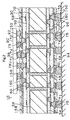
- Fig. 1 shows a sectional view of a printed wiring board
- Fig. 2 shows the printed wiring board 10 shown in Fig. 1 fitted to an IC chip 90 and mounted on a daughter board 94.
- a conductor circuit 34 is formed on both faces of a core substrate 30, and these conductor circuits are electrically connected through a through-hole 36.
- the conductor circuit 34 of the core substrate 30 is formed a conductor circuit 58 for forming a conductor circuit layer through an interlayer resin insulating layer 50.
- the conductor circuit 58 is connected to the conductor circuit 34 through a via hole 60.
- On the conductor circuit 58 is formed a conductor circuit 158 through an interlayer resin insulating layer 150.
- the conductor circuit 158 is connected to the conductor circuit 58 through a via hole 160 formed in the interlayer resin insulating layer 150.
- a solder resist layer 70 is formed by covering the conductor circuit 158 and the via hole 160, and a connecting pad 75 is formed by forming a nickel plated layer 72 and a gold plated layer 74 in an opening 71 provided in the solder resist layer 70. There are formed a solder bump 78U on the top face side of the connecting pad 75 and a BGA (ball grid alley) 78D on the bottom face of the connecting pad 75.
- BGA ball grid alley
- the solder bump 78U on the top face side of the printed wiring board 10 is connected to an electrode 92 of the IC chip 90 to compose an IC mounting printed wiring board, and the IC mounting printed wiring board is connected to a land 96 of the daughter board 94 through the BGA78D provided on the bottom face side.
- the surface of the solder resist layer corresponding to at least electronic parts mounting region is flattened.
- thermal expansion coefficient of the solder resist layer and the solder bump are different, contraction and expansion are repeated in the vicinity of the solder bump and the solder resist layer by thermal change.
- the volume of the solder resist layer in the vicinity of the solder bump is less, breakdown tends to occur. Therefore, the volume of largely stressed portion of the solder resist layer is increased by lessening flatness of the solder resist layer surface to some extent and the tress-concentrating bent portion is lessened, so as to improve heat cycle resistance.
- the flattened surface of the solder resist layer is desirably 0.8 ⁇ m to 3.0 ⁇ m in maximum surface roughness.
- Wettability of the under fill resin is easily improved by applying the roughening treatment to the surface of the solder resist layer flattened to some extent, so that under fill resin can be filled in a narrow gap portion in the boundary vicinity between the solder resist layer and the solder bump so as to improve connection reliability.
- the roughened surface of the solder resist layer is smaller than the maximum surface roughness of the flattened surface and 0.2 to 0.5 ⁇ m at an arithmetic mean roughness (Ra).
- the reason is that when the arithmetic mean roughness Ra is made within a range of 0.2 to 0.5 ⁇ m, adhesion to the under fill resin can be increased, and flux residue and cleaning residue are hardly remained on the solder resist surface. As a result, insulation reliability and connection reliability are easily improved.
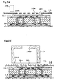
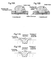
- an opening provided in the solder resist layer may be, as shown in Figs. 10A to 10B for instance, rectangular or trapezoidal in section.
- the solder bump portion filled in the opening and that exposed to the outside are smoothly continued, and the bent portion of the solder bump becomes small in the boundary with the solder resist layer, that is, the form of the solder bump is not extremely changed at the boundary portion with the solder resist layer so as not to concentrate stress.
- the solder bump is hard to be broken and connection reliability is improved.
- the shape of the opening may be a trapezoid in section wherein the difference D1-D2 is 5 ⁇ m to 20 ⁇ m.
- the difference D1-D2 is within such range, stress by thermal expansion coefficient difference between IC chip and print wiring board is hardly concentrated, so that connection reliability tends to be improved, and insulation performance between adjacent solder bumps can be secured. Further, migration is scarcely generated.
- two connecting pads positioned at center among connecting pads 75 provided on the top face are formed into the form of a land just above a via hole 160, and two connecting pads adjacent thereto are formed into the form of a pad adjacent to the land of the via hole 160, further, two connecting pads positioned at both ends are formed into the form of a pad consisting of a part of a wiring pattern of the conductor circuit 158, and solder bumps are formed on these connecting pads.
- connecting pads among connecting pads 75 on the bottom face, positioned at both ends, are formed into a land just above the via hole 160, and four connecting pads positioned at center are formed into a pad adjacent to the via hole 160.
- the via hole 160 as a connecting bad for forming the solder bump 78U is preferably a filled via, and an uneven amount of the filled via surface exposed from the surface of the interlayer resin insulating layer 150 is, as shown in Figs. 11A and 11B , desirably within a range of -5 ⁇ m to +5 ⁇ m to conductor thickness of the conductor circuit 158.
- the reason why the depressed or protruded amount of the filled-via surface is restricted to a mentioned above is due to the fact that when the depressed amount is more than 5 ⁇ m (-5 ⁇ m), the number of contact point defined by the solder ball and the connecting pad consisting of the filled-via is reduced, and wettability in case of forming the solder bump becomes poor, and entanglement of voids within the bump and missing bump tend to occur, while when the protruded amount of the filled-via surface is more than 5 ⁇ m (+ 5 ⁇ m), the thickness of the conductor circuit 158 becomes too large to be adaptable for fine pitched patterning.
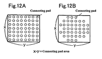
- the "electronic parts mounting region” in the invention substantially corresponds to a region forming conductor pads for mounting electronic parts such as connecting pads, filled via and the like (hereinafter, simply referred to as “connecting pad region”).
- Fig. 12A shows an embodiment of aligning all of outer peripheral connecting pads among connecting pads aligned in grid-like along each side of the rectangle
- Fig. 12B shows an embodiment of not aligning some of the outer peripheral connecting pads along each side of the rectangle, and in both cases, when the connecting pad is made a rectangle, a rectangular region determined to minimize the area surrounding all connecting pads is "connecting pad region”.
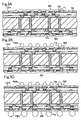
- Figs. 3A to 3C are views explaining steps for forming solder bumps on the printed wiring board 10.
- a flux layer 80 is formed for covering conductor pads formed in the openings 71 provided in the solder resist layer 70 on the top face side of the printed wiring board, i.e. the connecting pads 75 by a printing method (see Fig. 3A ).
- solder ball for example, made by Hitachi Metals or Tamura
- solder ball loader described later on (see Fig. 3B ).
- solder ball is desirable 40 ⁇ m or more and less than 200 ⁇ m in diameter.
- each solder ball does not drops on the corresponding connecting pad because it is too light in weight, while the diameter is 200 ⁇ m or more, each solder ball is too heavy to be assembled in the cylinder member, causing the presence of connecting pads with no solder balls mounted thereon.
- the solder ball having a diameter of 80 ⁇ m or less is desirable.
- solder ball 78L of a normal diameter (250 ⁇ m) is adsorbed and placed on the connecting pad 75 on the bottom face side of the printed wiring board 10 by using, e.g. an adsorption head described in Japanese patent No. 1975429 (see Fig. 3C ).
- solder bump 78U is formed at a pitch of 60 ⁇ m to 200 ⁇ m on the top face side of the printed wiring board 10 and 250 pieces of BGA 78D are formed at a pitch of about 2 mm on the bottom face side thereof, for example.
- the pitch of the solder bump is, i.e. a pitch of the connecting pad, and when the pitch of the connecting pad becomes less than 60 ⁇ m, it becomes difficult to manufacture the solder ball suitable for the pitch. On the other hand, when the pitch of the connecting pad is more than 200 ⁇ m, it becomes difficult to obtain a printed wiring board adaptable for fine patterning or narrow pitching.
- an IC mounting printed wiring board 10 is formed by mounting IC chips 90 through the solder bump 78U by reflowing, and the IC mounting printed wiring board 10 is mounted on a daughter board 94 through BGA 78D.
- solder ball loading device for loading very small solder balls 78s on the connecting pad of the above-described printed wiring board is explained by referring to Figs. 4A and 4B .
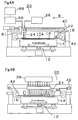
- Fig. 4A is an illustration showing the structure of the solder ball loader
- Fig. 4B is a view taken from an arrow B of the solder ball loader of Fig 4A .
- the solder ball loader 20 comprises an XY ⁇ suction table 14 for positioning and holding the printed wiring board 10, a vertical moving shaft 12 for moving the XY ⁇ suction table 14 up and down, a ball aligning mask 16 with an opening corresponding to the connecting pad 75 of the printed wiring board, a mounting cylinder (cylinder member) 24 for guiding the solder balls moving on the ball aligning mask 16, a suction box 26 for giving negative pressure to the mounting cylinder 24, a solder ball removing cylinder 61 for recovering excessive solder balls, a suction box 66 for giving negative pressure to the solder ball removing cylinder 61, an adsorbed ball removing and adsorbing device 68 for holding the collected solder balls, a mask clamp 44 for clamping the ball aligning mask 16, an X-axis direction moving shaft 40 for sending the mounting cylinder 24 and the solder ball removing cylinder 61 to the X-axis direction, a moving shaft supporting guide 42 for supporting the X-axis direction moving shaft 40, an alignment camera 46 for taking an
- a plurality of the mounting cylinders 24 and the solder ball removing cylinder 61 are arranged in the Y-axis direction by corresponding to size of the connecting pad regions. Further, the size may correspond to a plurality of the connecting pad areas.
- the Y-axis direction is expedient and may be aligned in the X-axis direction.
- the XY ⁇ suction table 14 functions as positioning, adsorption, maintenance and correction of the solder ball mounted printed wiring board 10.
- the alignment camera 46 detects an alignment mark of the printed wiring board 10 on the XY ⁇ suction table 14 to regulate a position between the printed wiring board and the ball aligning mask 16 based on the detected position.
- the residue detecting sensor 18 detects the residue of the solder balls by an optical method.
- an alignment mark 34M of the printed wiring board 10 is recognized by the alignment camera 46, and the position of the printed wiring board 10 in relation to the ball aligning mask 16 is corrected by the suction table 14. That is, openings 16a of the ball aligning mask 16 are adjusted for corresponding to the connecting pads 75 of the printed wiring board 10 in position, respectively.
- solder balls are mounted to a printed wiring board of worksheet size for constructing a plurality of printed wiring boards, and after forming solder bumps, the worksheet size board is cut into respective multilayer printed wiring boards.
- solder balls 78s are quantitatively supplied from a solder ball supplying device 22 to the side of the mounting cylinder 24.
- solder ball any commercial item (a product of Hitachi Metals, for example) may be used or, solder balls may be manufactured according to the manufacturing device and method described in Japanese unexamined patent application No. 2001-226705 .
- solder balls are placed on a metal plate (e.g. nickel plate of about 25 ⁇ m thick) having a square slit (opening) which length and breadth are smaller than a designated diameter of the solder ball by 1 ⁇ m, and the solder balls are rolled thereon and dropped from the slit. Then, balls having smaller diameters than designated are removed. Thereafter, the solder balls remained on the metal plate are classified by a metal plate having a square slit which length and breadth are larger than the designated diameter of the solder ball by 1 ⁇ m, and solder balls dropped from the slit are collected so as to obtain the solder balls each having a diameter substantially equal to the designated diameter.
- a metal plate e.g. nickel plate of about 25 ⁇ m thick
- solder balls are rolled thereon and dropped from the slit.
- balls having smaller diameters than designated are removed.
- solder balls remained on the metal plate are classified by a metal plate having a square slit which length and breadth are larger than
- solder balls 78s are assembled on the ball aligning mask 16 right under the opening 24A of the mounting cylinder 24 by adsorbing air from the suction portion 24B at a running speed of 5 m/sec to 35 m/sec in a gap between the mounting cylinder and the printed wiring board.
- the mounting cylinders 24 aligned along the Y-axis of the printed wiring board 10 are sent to the horizontal direction along the X-axis by means of the X-axis direction moving shaft 40.
- the solder balls 78s assembled on the ball aligning mask 16 are moved with the movement of the mounting cylinder 24, dropped to the corresponding connecting pads 75 of the printed wiring board 10 through the openings 16a of the ball aligning mask 16 and loaded.
- the solder balls 78s are successively aligned on the whole connecting pads on the side of the printed wiring board 10.
- the excessive solder balls 78s are guided to a place having no opening 16a on the ball aligning mask 16, then adsorbed and removed by the solder ball removing cylinder 61.
- the solder balls 78s are assembled by positioning the mounting cylinder 24 on the upper part of the ball aligning mask 16 and adsorbing air from the suction portion 24B on the top of the mounting cylinder 24, the assembled solder balls 78s are moved on the ball aligning mask 16 by moving the mounting cylinder 24 in the horizontal direction, and the solder balls 78s can be dropped to the respective connecting pads 75 of the printed wiring board 10 through the respective openings 16a of the ball aligning mask 16.
- solder balls 78s can certainly be mounted on the whole of the connecting pads 75 of the printed wiring board 10. Further, since the solder balls 78s can be moved with no contact, the solder balls can be mounted on the connecting pads 75 without damage, which is different from a printing method with the use of a conventional squeeze, and the solder bumps 78U can be equalized in height.
- the fine solder balls could certainly be placed on the connecting pads, even in the printed wiring board having such a narrow pitch alignment that the connecting pad pitch is 60 to 200 ⁇ m and the solder resist opening diameter is 40 to 150 ⁇ m, in the whole of bumps, stable bumps having substantially uniform heights can be formed.
- solder balls are guided by suction force so as to prevent aggregation and adhesion of solder balls. Further, adjusting number of the mounting cylinder 24 so as to be applied to many forms and small production enables the applicability to various sizes of the works (multilayer printed wiring board of work sheet size).
- the mounting cylinders 24 are aligned in the Y direction by corresponding to width of the work (printed wiring board of work sheet size), so that the solder balls can positively be mounted on the whole of connecting pads 75 of the printed wiring boards by simply sending a plurality of mounting cylinders 24 to the vertical direction (X direction) in relation to the row direction.
- solder balls 78s remained on the ball aligning mask 16 can be collected by the solder ball removing cylinder 61, so that there are no problem such that excessive solder ball are remained to cause any trouble and the like.
- solder balls mounted on the connecting pads of the wiring substrate become solder bumps having predetermined height by means of a reflow treatment, IC chips are mounted on the substrate through such solder bumps, and the printed wiring board according to the present invention is manufactured.
- a double sided copper-clad laminate e.g. "MCL-E-67” made by Hitachi Chemical
- a through-hole conductor and a conductor circuit by a known method.
- insulating layers and conductor circuit layers are alternately laminated by a known method (e.g.
- Such connecting pads are formed by a method similar to that described in Japanese unexamined patent application No. 2000-357762 .
- the pattern (opening diameter, pitch, arrangement, etc.) of a plated resist is changed.
- Formation of a solder resist layer is that screen printing is carried out under the following printing condition with the use of a commercial solder resist to form a solder resist layer having a thickness of 15 to 25 ⁇ m (on the connecting pad) for covering the connecting pad.
- Solder resist ink "RPZ-1" made by Hitachi Kogyo Ink viscosity : 45 ⁇ 15 Pa ⁇ s Screen : polyester fiber (130 to 300 mesh) Squeeze speed : 100 to 200 mm/sec
- thickness of the solder resist layer is 25 ⁇ m.
- a photo mask having a pattern (mask pattern) of opening of solder resist thereon is exposed to ultraviolet ray of 100 to 1000 mJ under the state of adhering to the solder resist layer, and developed by using a horizontal type developer under the following development conditions, thereby forming an opening of 40-150 ⁇ m in diameter on the connecting pad.
- a horizontal developing device comprising a conveyor for bringing the substrate in a developing treatment zone and conveying the developing treatment zone and a plurality of spray nozzles positioned at top and bottom of the substrate for adjusting spray pressure is used.
- an opening (diameter of an opening of the solder resist layer surface is equal to diameter of an opening of the connecting pad) of about 80 ⁇ m in diameter is formed by facing the solder resist face downwardly under the state of not oscillating the slit nozzle positioned at the lower part and by developing with the use of a sodium carbonate (Na 2 CO 3 ) solution of 10 g/L in concentration.
- the ball aligning mask a metal mask made of Ni having an opening of 100 ⁇ m in diameter at the position corresponding to the connecting pad of the printed wiring board is used. It is also possible to use ball aligning masks of SUS and polyimide.
- an opening diameter formed in the ball aligning mask is preferably 1.1 to 1.5 times the ball diameter used, and a thickness of the ball aligning mask is preferably 1/2 to 3/4 of the diameter of the solder ball used.
- Sn/Pb is used for the solder ball, however, Pb free solder consisting of at least one metal and Sn selected from the group of Ag, Co, In, Bi, Zn and the like may also be used. Further, air is adsorbed from the top of the mounting cylinder, and the air speed in a gap between the mounting cylinder and the printed wiring board is regulated to 5 to 35 m/sec for assembling the solder balls within the mounting cylinder.
- the mounting cylinder is moved at 10 to 40 mm/sec to roll the solder balls, and the solder balls are dropped from the respective openings of the ball aligning mask and mounted on the corresponding connection pads.
- solder ball aligning mask and the printed wiring board are separately taken out of the solder ball loader, and finally, the printed wiring board is put in the reflow furnace set at 230°C to form a solder bump.
- a diameter of the solder bump protruded from the solder resist surface is measured by a laser microscope ("WYKO NT-2000" made by Veeco) . As a result, the diameter is 84 ⁇ m
- an IC chip is mounted through the solder bumps, and the IC chip mounted printed wiring board is manufactured by filling a commercial under fill resin between the IC chip and the solder resist.
- the printed wiring board is manufactured in the same manner as in Example 1. As a result, the solder bump diameter becomes 100 ⁇ m.
- the printed wiring board is manufactured in the same manner as in Example 1. As a result, the solder bump diameter becomes 120 ⁇ m.
- the printed wiring board is manufactured in the same manner as in Example 1. As a result, the solder bump diameter becomes 135 ⁇ m.
- the printed wiring board is manufactured in the same manner as in Example 1. As a result, there is formed a trapezoidal opening such as 85 ⁇ m of the top opening diameter and 80 ⁇ m of the bottom opening diameter, but the solder bump diameter becomes the same 84 ⁇ m as in Example 1.
- the solder resist layer opening is made a trapezoid in section as shown in Fig. 10B , that is, it is understood that the form (circled with a dotted line) of the boundary portion of the solder bump and the solder resist layer surface is different by tapering.
- the printed wiring board is manufactured in the same manner as in Example 5. As a result, the solder bump diameter becomes 105 ⁇ m.
- the printed wiring board is manufactured in the same manner as in Example 5. As a result, the solder bump diameter becomes 128 ⁇ m.
- the printed wiring board is manufactured in the same manner as in Example 5. As a result, the solder bump diameter becomes 145 ⁇ m.
- the printed wiring board is manufactured in the same manner as in Example 5. As a result, there is formed a trapezoidal opening which top opening diameter is 90 ⁇ m and bottom opening diameter is 80 ⁇ m, and the solder bump diameter becomes 94 ⁇ m.
- the printed wiring board is manufactured in the same manner as in Example 6. As a result, there is formed a trapezoidal opening which top opening diameter is 90 ⁇ m and bottom opening diameter is 80 ⁇ m, and the solder bump diameter becomes 113 ⁇ m.
- the printed wiring board is manufactured in the same manner as in Example 7. As a result, there is formed a trapezoidal opening which top opening diameter is 90 ⁇ m and bottom opening diameter is 80 ⁇ m, and the solder bump diameter becomes 135 ⁇ m.
- the printed wiring board is manufactured in the same manner as in Example 8. As a result, there is formed a trapezoidal opening which top opening diameter is 90 ⁇ m and bottom opening diameter is 80 ⁇ m, and the solder bump diameter becomes 155 ⁇ m.
- the printed wiring board is manufactured in the same manner as in Example 9. As a result, there is formed a trapezoidal opening which top opening diameter is 100 ⁇ m and bottom opening diameter is 80 ⁇ m, and the solder bump diameter becomes 105 ⁇ m.
- the printed wiring board is manufactured in the same manner as in Example 10. As a result, there is formed a trapezoidal opening which top opening diameter is 100 ⁇ m and bottom opening diameter is 80 ⁇ m, and the solder bump diameter becomes 125 ⁇ m.
- the printed wiring board is manufactured in the same manner as in Example 11. As a result, there is formed a trapezoidal opening which top opening diameter is 100 ⁇ m and bottom opening diameter is 80 ⁇ m, and the solder bump diameter becomes 150 ⁇ m.
- the printed wiring board is manufactured in the same manner as in Example 12. As a result, there is formed a trapezoidal opening which top opening diameter is 100 ⁇ m and bottom opening diameter is 80 ⁇ m, and the solder bump diameter becomes 170 ⁇ m.
- the printed wiring board is manufactured in the same manner as in Example 1. As a result, the solder bump diameter becomes 63 ⁇ m.
- the printed wiring board is manufactured in the same manner as in Example 17. As a result, the solder bump diameter becomes 75 ⁇ m.
- the printed wiring board is manufactured in the same manner as in Example 17. As a result, the solder bump diameter becomes 90 ⁇ m.
- the printed wiring board is manufactured in the same manner as in Example 17. As a result, the solder bump diameter becomes 102 ⁇ m.
- the connecting pad of 70 ⁇ m in diameter is formed at 100 ⁇ m pitch in the same manner as in Example 17, and the diameter of the mask for forming the opening of the solder resist layer is changed so that an opening of 65 ⁇ m in top opening diameter and 60 ⁇ m in bottom opening diameter is formed, and the solder bump of 63 ⁇ m in diameter is used, the printed wiring board is manufactured in the same manner as in Example 5. As a result, the solder bump diameter becomes 68 ⁇ m.
- the connecting pad of 70 ⁇ m in diameter is formed at 100 ⁇ m pitch in the same manner as in Example 17, and the diameter of the mask for forming the opening of the solder resist layer is changed so that an opening of 65 ⁇ m in top opening diameter and 60 ⁇ m in bottom opening diameter is formed, and the solder bump of 70 ⁇ m in diameter is used, the printed wiring board is manufactured in the same manner as in Example 5. As a result, the solder bump diameter becomes 80 ⁇ m.
- the connecting pad of 70 ⁇ m in diameter is formed at 100 ⁇ m pitch in the same manner as in Example 17, and the diameter of the mask for forming the opening of the solder resist layer is changed so that an opening of 65 ⁇ m in top opening diameter and 60 ⁇ m in bottom opening diameter is formed, and the solder bump of 80 ⁇ m in diameter is used, the printed wiring board is manufactured in the same manner as in Example 5. As a result, the solder bump diameter becomes 96 ⁇ m.
- the connecting pad of 70 ⁇ m in diameter is formed at 100 ⁇ m pitch in the same manner as in Example 17,- and the diameter of the mask for forming the opening of the solder resist layer is changed so that an opening of 65 ⁇ m in top opening diameter and 60 ⁇ m in bottom opening diameter is formed, and the solder bump of 95 ⁇ m in diameter is used, the printed wiring board is manufactured in the same manner as in Example 5. As a result, the solder bump diameter becomes 110 ⁇ m.
- the printed wiring board is manufactured in the same manner as in Example 21. As a result, there is formed a trapezoidal opening of 70 ⁇ m in top opening diameter and 60 ⁇ m in bottom opening diameter, and the solder bump diameter becomes 73 ⁇ m.
- the printed wiring board is manufactured in the same manner as in Example 22. As a result, there is formed a trapezoidal opening of 70 ⁇ m in top opening diameter and 60 ⁇ m in bottom opening diameter, and the solder bump diameter becomes 88 ⁇ m.
- the printed wiring board is manufactured in the same manner as in Example 23. As a result, there is formed a trapezoidal opening of 70 ⁇ m in top opening diameter and 60 ⁇ m in bottom opening diameter, and the solder bump diameter becomes 105 ⁇ m.
- the printed wiring board is manufactured in the same manner as in Example 24. As a result, there is formed a trapezoidal opening of 70 ⁇ m in top opening diameter and 60 ⁇ m in bottom opening diameter, and the solder bump diameter becomes 120 ⁇ m.
- the printed wiring board is manufactured in the same manner as in Example 25. As a result, there is formed a trapezoidal opening of 80 ⁇ m in top opening diameter and 60 ⁇ m in bottom opening diameter, and the solder bump diameter becomes 84 ⁇ m.
- the printed wiring board is manufactured in the same manner as in Example 26. As a result, there is formed a trapezoidal opening of 80 ⁇ m in top opening diameter and 60 ⁇ m in bottom opening diameter, and the solder bump diameter becomes 100 ⁇ m.
- the printed wiring board is manufactured in the same manner as in Example 27. As a result, there is formed a trapezoidal opening of 80 ⁇ m in top opening diameter and 60 ⁇ m in bottom opening diameter, and the solder bump diameter becomes 120 ⁇ m.
- the printed wiring board is manufactured in the same manner as in Example 28. As a result, there is formed a trapezoidal opening of 80 ⁇ m in top opening diameter and 60 ⁇ m in bottom opening diameter, and the solder bump diameter becomes 135 ⁇ m.
- the printed wiring board is manufactured in the same manner as in Example 1. As a result, the solder bump diameter becomes 108 ⁇ m.
- the printed wiring board is manufactured in the same manner as in Example 33. As a result, the solder bump diameter becomes 130 ⁇ m.
- the printed wiring board is manufactured in the same manner as in Example 33. As a result, the solder bump diameter becomes 155 ⁇ m.
- the printed wiring board is manufactured in the same manner as in Example 33. As a result, the solder bump diameter becomes 175 ⁇ m.
- the connecting pad of 150 ⁇ m in diameter is formed at 190 ⁇ m pitch in the same manner as in Example 33, and the diameter of the mask for forming the opening of the solder resist layer is changed so that an opening of 108 ⁇ m in top opening diameter and 103 ⁇ m in bottom opening diameter is formed, and the solder bump of 105 ⁇ m in diameter is used, the printed wiring board is manufactured in the same manner as in Example 33. As a result, the solder bump diameter becomes 113 ⁇ m.
- the connecting pad of 150 ⁇ m in diameter is formed at 190 ⁇ m pitch in the same manner as in Example 33, and the diameter of the mask for forming the opening of the solder resist layer is changed so that an opening of 108 ⁇ m in top opening diameter and 103 ⁇ m in bottom opening diameter is formed, and the solder bump of 125 ⁇ m in diameter is used, the printed wiring board is manufactured in the same manner as in Example 33. As a result, the solder bump diameter becomes 135 ⁇ m.
- the connecting pad of 150 ⁇ m in diameter is formed at 190 ⁇ m pitch in the same manner as in Example 33, and the diameter of the mask for forming the opening of the solder resist layer is changed so that an opening of 108 ⁇ m in top opening diameter and 103 ⁇ m in bottom opening diameter is formed, and the solder bump of 155 ⁇ m in diameter is used, the printed wiring board is manufactured in the same manner as in Example 33. As a result, the solder bump diameter becomes 162 ⁇ m.
- the connecting pad of 150 ⁇ m in diameter is formed at 190 ⁇ m pitch in the same manner as in Example 33, and the diameter of the mask for forming the opening of the solder resist layer is changed so that an opening of 108 ⁇ m in top opening diameter and 103 ⁇ m in bottom opening diameter is formed, and the solder bump of 180 ⁇ m in diameter is used, the printed wiring board is manufactured in the same manner as in Example 33. As a result, the solder bump diameter becomes 185 ⁇ m.
- the printed wiring board is manufactured in the same manner as in Example 37. As a result, the solder bump diameter becomes 118 ⁇ m.
- the printed wiring board is manufactured in the same manner as in Example 38. As a result, the solder bump diameter becomes 140 ⁇ m.
- the printed wiring board is manufactured in the same manner as in Example 39. As a result, the solder bump diameter becomes 170 ⁇ m.
- the printed wiring board is manufactured in the same manner as in Example 40. As a result, the solder bump diameter becomes 192 ⁇ m.
- the printed wiring board is manufactured in the same manner as in Example 41. As a result, there is formed a trapezoidal opening of 123 ⁇ m in top opening diameter and 103 ⁇ m in bottom opening diameter, and the solder bump diameter becomes 129 ⁇ m.
- the printed wiring board is manufactured in the same manner as in Example 42. As a result, there is formed a trapezoidal opening of 123 ⁇ m in top opening diameter and 103 ⁇ m in bottom opening diameter, and the solder bump diameter becomes 129 ⁇ m.
- the printed wiring board is manufactured in the same manner as in Example 43. As a result, there is formed a trapezoidal opening of 123 ⁇ m in top opening diameter and 103 ⁇ m in bottom opening diameter, and the solder bump diameter becomes 185 ⁇ m.
- the printed wiring board is manufactured in the same manner as in Example 44. As a result, there is formed a trapezoidal opening of 123 ⁇ m in top opening diameter and 103 ⁇ m in bottom opening diameter, and the solder bump diameter becomes 210 ⁇ m.
- the printed wiring board is manufactured in the same manner as in Example 1. As a result, the solder bump diameter becomes 160 ⁇ m.
- the printed wiring board is manufactured in the same manner as in Examples 1 to 48.
- the printed wiring board is manufactured in the same manner as in Example 1. As a result, solder could not completely be filled in the solder resist opening.
- Examples 1 to 48 and Reference Example 1 completely filling the solder bump in the opening of the solder resist are liable to improve connection reliability as compared with Comparative Example. This is because volume of the solder bump is large and stress owing to thermal expansion difference between IC chips and printed wiring boards is more mitigated, or because of no gap between solder resists and solder bumps, voids are difficult to generate within under fill, or no residuum of flux and clearing solution.
- connection reliability is liable to improve in order of (1) when the ratio (W/D) of a solder bump diameter W to a solder resist opening diameter D is within a range of 1.05 to 1.7, (2) when the solder resist opening is a tapered form wherein the top opening diameter is larger than the bottom opening diameter, and the ratio (W/D) is within a range of 1.05 to 1.5, and (3) when the solder resist opening is a tapered form wherein the top opening diameter is larger than the bottom opening diameter, and the ratio (W/D) is within a range of 1.05 to 1.25.
- the solder bump tends to bend at the boundary with the solder resist layer surface (the portion of solder bump exposed from the surface of solder resist layer to the outside, which is circled with a dotted line in Fig. 10A ), and stress tends to concentrate in this bent portion, so that connection reliability is improved when a bending degree is made small.
- the bending degree is correlated to the ratio (W/D), and it is assumed that connection reliability is easily improved when the ratio (W/D) is 1.7 or less.
- the ratio (W/D) is less than 1.05, it is presumed that it happens that the opening of the solder resist layer is not filled completely with the solder bump. And, when the shape of the opening formed in the solder resist layer is a trapezoidal one (top opening diameter D1 is larger than the bottom opening diameter D2), it is presumed that the bending degree becomes small as shown in Fig. 10B so that the solder bump is hardly broken.
- solder volume is large, so that significance of applying to the printed wiring board having a large connecting pad region such as about 2000 to 30000 solder bumps is large.
- connecting pad region rectangular region including outermost connecting pad
- shearing stress due to thermal expansion coefficient difference between IC chips and printed wiring boards becomes large.
- the IC mounting printed wiring board is manufactured in the same manner as in each example, and described as Examples 49 to 66.
- an uneven amount of the solder resist surface is measured at the same spot by means of a surface roughness measuring instrument (e.g. "SURFCOM 480A” made by Tokyo Seimitsu or “WYKO N-2500” by Veeco).
- a surface roughness measuring instrument e.g. "SURFCOM 480A” made by Tokyo Seimitsu or “WYKO N-2500” by Veeco.
- the measured spots are the solder resist layer surface positioned at the upper part of the connecting pad and the solder resist layer surface of the adjacent connecting pad non-forming portion (see Fig. 8 ). That is, the uneven amount of the solder resist layer surface due to presence of the connecting pad is measured, and the maximum value (max) and the minimum value (min) of the 5-point measured results are described. These measurement results are shown in Table 3 (before flattening treatment) and Table 4 (after flattening treatment).
- the IC mounting printed wiring board is manufactured in the same manner as in each example, and described here as Examples 67 to 84.
- surface roughness of the solder resist surface is measured at 10 spots at random with reference length 5 ⁇ m by means of a surface roughness measuring instrument (e.g. "SURFCOM 480A” made by Tokyo Seimitsu or “WYKO N-2500” by Veeco).
- a surface roughness measuring instrument e.g. "SURFCOM 480A” made by Tokyo Seimitsu or "WYKO N-2500” by Veeco.
- surface roughness Ra means "arithmetic mean roughness Ra” prescribed by JIS B0601.
- the reason why Ra has a range in the above measured result is because that among respective Ra at the measured 10 spots, there are described the most minimum Ra as Ra(min) and the most maximum Ra as Ra(max).
- surface roughening measurement is carried out at random 10 spots in the solder resist layer surface corresponding to the conductor circuit (pad) forming region and the conductor circuit non-forming region, but not in the boundary vicinity of the conductor circuit forming region and the conductor circuit non-forming region.
- a heat cycle test is carried out for the IC mounting printed wiring board manufactured according to Examples 5,6, 9, 10, 13, 14, 21, 22, 25, 26, 29, 30, 37, 38, 41, 42, 45 and 46, Examples 49 to 66, and Examples 67 to 84 by repeating 2500 times of 1 cycle of -55°C x 30 min and 125°C x 30 min after leaving in an atmosphere such as temperature of 85°C and humidity of 85% for 24 hours. Electric resistances after 1750 cycles and 2000 cycles are measured, and the rate (100X (measured value-initial value)/initial value) (%) of change with the initial value is sought. The case of the rate of change within ⁇ 10 is evaluated as "good” and shown by O, and other cases are evaluated as "no good" and shown by x.
- Example 71 0.8 3.2 0.2 0.5 0. 7 ⁇ ⁇
- Example 72 0.8 3.2 0.2 0 . 5 0.7 ⁇ ⁇
- Example 73 0.7 3 . 0 0.1 0 . 5 0.6 ⁇ ⁇
- Example 74 0.7 3.0 0.1 0.5 0.6 ⁇ ⁇
- Example 75 0.8 3. 2 0.2 0 . 5 0 . 7 ⁇ ⁇
- Example 76 0.8 3.1 0 . 2 0.5 0 . 7 ⁇ ⁇
- Example 77 0.8 3 . 0 0.2 0.6 0.7 ⁇ ⁇
- Example 78 0.8 3 . 2 0.2 0 . 6 0 .
- Example 79 0.7 3.1 0.1 0 . 5 0 . 6 ⁇ ⁇
- Example 80 0.8 3.0 0.1 0.5 0.6 ⁇ ⁇
- Example 81 0.7 3.0 0.2 0.5 0.7 ⁇ ⁇
- Example 82 0.8 3 . 2 0.1 0 . 5 0 . 6 ⁇ ⁇
- Example 83 0.8 3.2 0.1 0.5 0.6 ⁇ ⁇
- Example 84 0.7 3 . 0 0.1 0 . 5 0 . 6 ⁇ ⁇
- connection reliability is improved when the uneven amount of the solder resist layer surface is preferably 0.8 ⁇ m to 3.0 ⁇ m and further, the arithmetic mean roughness Ra thereof is 0.2 ⁇ m to 0.5 ⁇ m.
- the solder bump in the invention is large in bump diameter so as to increase bump height for its degree. Therefore, as the space between the solder resist layer surface and the IC chip becomes large, under fill is difficult to be filled and void tends to generate in the under fill.
- the moving speed of the under fill is liable to depend on the space between the solder resist layer surface and the IC chip, it is considered that unevenness of the solder resist layer surface is 2 ⁇ m or less.
- the IC mounting printed wiring board manufactured according to Examples 1 to 84 and Comparative Example are left in an atmosphere of 85°C in temperature and 85% in humidity for 100 hours by applying voltage of 3.3V between dependent solder bumps (electrically not connected solder bumps). After leaving as they are, insulation resistance between voltage-applied solder bumps is measured. The value of more than or equal to 10 7 Q is evaluated as good and the value of less than 10 7 Q is evaluated as no good. As a result, Examples 1 to 86 are recognized as good, while Comparative Example is as no good.
- the invention proposes a printed wiring board having excellent insulation reliability and insulation reliability by making the ratio (W/D) of a solder bump diameter W to an opening diameter D provided in the opening of a solder resist layer 1.05 to 1. 7 even with such narrow pitch structure that a pitch of the solder bump is 200 ⁇ m or less.
Landscapes
- Engineering & Computer Science (AREA)
- Manufacturing & Machinery (AREA)
- Microelectronics & Electronic Packaging (AREA)
- Mechanical Engineering (AREA)
- Electric Connection Of Electric Components To Printed Circuits (AREA)
- Manufacturing Of Printed Wiring (AREA)
Applications Claiming Priority (2)
| Application Number | Priority Date | Filing Date | Title |
|---|---|---|---|
| JP2005192863 | 2005-06-30 | ||
| PCT/JP2006/313343 WO2007004658A1 (ja) | 2005-06-30 | 2006-06-28 | プリント配線板 |
Publications (2)
| Publication Number | Publication Date |
|---|---|
| EP1887846A1 true EP1887846A1 (de) | 2008-02-13 |
| EP1887846A4 EP1887846A4 (de) | 2010-08-11 |
Family
ID=37604519
Family Applications (1)
| Application Number | Title | Priority Date | Filing Date |
|---|---|---|---|
| EP06780770A Withdrawn EP1887846A4 (de) | 2005-06-30 | 2006-06-28 | Leiterplatte |
Country Status (7)
| Country | Link |
|---|---|
| US (3) | US8017875B2 (de) |
| EP (1) | EP1887846A4 (de) |
| JP (1) | JP5021473B2 (de) |
| KR (1) | KR100905685B1 (de) |
| CN (2) | CN101854771A (de) |
| TW (1) | TW200718298A (de) |
| WO (1) | WO2007004658A1 (de) |
Cited By (2)
| Publication number | Priority date | Publication date | Assignee | Title |
|---|---|---|---|---|
| CN102800635A (zh) * | 2011-05-23 | 2012-11-28 | 三菱电机株式会社 | 半导体装置 |
| CN102239753B (zh) * | 2008-12-05 | 2013-11-06 | 揖斐电株式会社 | 多层印刷线路板和多层印刷线路板的制造方法 |
Families Citing this family (43)
| Publication number | Priority date | Publication date | Assignee | Title |
|---|---|---|---|---|
| JP4576270B2 (ja) * | 2005-03-29 | 2010-11-04 | 昭和電工株式会社 | ハンダ回路基板の製造方法 |
| JP4997105B2 (ja) * | 2005-05-23 | 2012-08-08 | イビデン株式会社 | プリント配線板およびその製造方法 |
| JP5021473B2 (ja) * | 2005-06-30 | 2012-09-05 | イビデン株式会社 | プリント配線板の製造方法 |
| EP1887845A4 (de) | 2005-06-30 | 2010-08-11 | Ibiden Co Ltd | Leiterplatte |
| WO2007007865A1 (en) | 2005-07-11 | 2007-01-18 | Showa Denko K.K. | Method for attachment of solder powder to electronic circuit board and solder-attached electronic circuit board |
| WO2007029866A1 (en) * | 2005-09-09 | 2007-03-15 | Showa Denko K.K. | Method for attachment of solder powder to electronic circuit board and soldered electronic circuit board |
| CN101888747B (zh) * | 2006-01-27 | 2012-09-05 | 揖斐电株式会社 | 印刷线路板的制造方法 |
| WO2008016128A1 (en) * | 2006-08-03 | 2008-02-07 | Showa Denko K.K. | Production method of soldier circuit board |
| CN101296570A (zh) * | 2007-04-25 | 2008-10-29 | 富葵精密组件(深圳)有限公司 | 电路板及其制作方法 |
| US8455766B2 (en) * | 2007-08-08 | 2013-06-04 | Ibiden Co., Ltd. | Substrate with low-elasticity layer and low-thermal-expansion layer |
| JPWO2009144846A1 (ja) * | 2008-05-30 | 2011-10-06 | イビデン株式会社 | 半田ボール搭載方法 |
| US7705447B2 (en) * | 2008-09-29 | 2010-04-27 | Intel Corporation | Input/output package architectures, and methods of using same |
| KR101002680B1 (ko) * | 2008-10-21 | 2010-12-21 | 삼성전기주식회사 | 반도체 패키지 및 그 제조 방법 |
| TWI468093B (zh) * | 2008-10-31 | 2015-01-01 | Princo Corp | 多層基板之導孔結構及其製造方法 |
| CN101917818B (zh) * | 2009-09-25 | 2012-08-22 | 昆山市华升电路板有限公司 | 电路板的焊盘结构及其制作方法 |
| JP5807221B2 (ja) | 2010-06-28 | 2015-11-10 | アユミ工業株式会社 | 接合構造体製造方法および加熱溶融処理方法ならびにこれらのシステム |
| US9706652B2 (en) | 2010-12-24 | 2017-07-11 | Lg Innotek Co., Ltd. | Printed circuit board and method for manufacturing same |
| KR101231522B1 (ko) * | 2010-12-24 | 2013-02-07 | 엘지이노텍 주식회사 | 인쇄회로기판 및 그의 제조 방법 |
| US8643196B2 (en) * | 2011-07-27 | 2014-02-04 | Taiwan Semiconductor Manufacturing Company, Ltd. | Structure and method for bump to landing trace ratio |
| US20130168132A1 (en) * | 2011-12-29 | 2013-07-04 | Sumsung Electro-Mechanics Co., Ltd. | Printed circuit board and method of manufacturing the same |
| JP5502139B2 (ja) * | 2012-05-16 | 2014-05-28 | 日本特殊陶業株式会社 | 配線基板 |
| FR2991108A1 (fr) * | 2012-05-24 | 2013-11-29 | St Microelectronics Sa | Ligne coplanaire blindee |
| JP6069960B2 (ja) * | 2012-08-30 | 2017-02-01 | 凸版印刷株式会社 | 半導体パッケージの製造方法 |
| KR101497840B1 (ko) * | 2013-12-02 | 2015-03-02 | 삼성전기주식회사 | 솔더레지스트 개구 구조 및 회로 기판 |
| JP2016015432A (ja) * | 2014-07-03 | 2016-01-28 | イビデン株式会社 | 回路基板及びその製造方法 |
| KR102214512B1 (ko) | 2014-07-04 | 2021-02-09 | 삼성전자 주식회사 | 인쇄회로기판 및 이를 이용한 반도체 패키지 |
| US9699921B2 (en) * | 2014-08-01 | 2017-07-04 | Fujikura Ltd. | Multi-layer wiring board |
| JP6329027B2 (ja) * | 2014-08-04 | 2018-05-23 | ミネベアミツミ株式会社 | フレキシブルプリント基板 |
| JP2016134409A (ja) * | 2015-01-16 | 2016-07-25 | イビデン株式会社 | プリント配線板 |
| KR102532200B1 (ko) * | 2015-12-09 | 2023-05-12 | 삼성전자 주식회사 | 테스트 패턴, 반도체 소자의 테스트 방법, 및 집적 회로의 레이아웃 설계를 위한 컴퓨터 구현 방법 |
| CN107732488A (zh) * | 2016-08-10 | 2018-02-23 | 泰科电子(上海)有限公司 | 连接件 |
| US10164358B2 (en) * | 2016-09-30 | 2018-12-25 | Western Digital Technologies, Inc. | Electrical feed-through and connector configuration |
| FR3069128B1 (fr) * | 2017-07-13 | 2020-06-26 | Safran Electronics & Defense | Fixation d'un cms sur une couche isolante avec un joint de brasure dans une cavite realisee dans une couche isolante |
| JP6991014B2 (ja) * | 2017-08-29 | 2022-01-12 | キオクシア株式会社 | 半導体装置 |
| US20190366460A1 (en) * | 2018-06-01 | 2019-12-05 | Progress Y&Y Corp. | Soldering apparatus and solder nozzle module thereof |
| US11488918B2 (en) * | 2018-10-31 | 2022-11-01 | Intel Corporation | Surface finishes with low rBTV for fine and mixed bump pitch architectures |
| CN111334750B (zh) * | 2020-03-11 | 2022-02-01 | 京东方科技集团股份有限公司 | 一种soi精细掩模版及其制作方法 |
| CN111640719B (zh) * | 2020-06-01 | 2022-04-01 | 厦门通富微电子有限公司 | 一种半导体器件及其制作方法 |
| KR102909754B1 (ko) * | 2020-06-12 | 2026-01-09 | 엘지이노텍 주식회사 | 인쇄회로기판 및 이의 제조 방법 |
| US20220069489A1 (en) * | 2020-08-28 | 2022-03-03 | Unimicron Technology Corp. | Circuit board structure and manufacturing method thereof |
| EP4102943A1 (de) * | 2021-06-11 | 2022-12-14 | ZF CV Systems Europe BV | Leiterplatte (pcb) und verfahren zur herstellung davon |
| CN113524885B (zh) * | 2021-07-17 | 2022-07-08 | 江苏本川智能电路科技股份有限公司 | 一种厚铜板阻焊印刷设备及其印刷方法 |
| JP2025145077A (ja) * | 2024-03-21 | 2025-10-03 | 株式会社東芝 | ワイヤボンディング装置及び制御方法 |
Family Cites Families (55)
| Publication number | Priority date | Publication date | Assignee | Title |
|---|---|---|---|---|
| JPS59996A (ja) | 1982-06-25 | 1984-01-06 | 株式会社日立製作所 | 基板の接続構造 |
| US5118027A (en) * | 1991-04-24 | 1992-06-02 | International Business Machines Corporation | Method of aligning and mounting solder balls to a substrate |
| JPH05121411A (ja) * | 1991-10-25 | 1993-05-18 | Rohm Co Ltd | 電子部品における接続用バンプの形成方法 |
| US5329423A (en) * | 1993-04-13 | 1994-07-12 | Scholz Kenneth D | Compressive bump-and-socket interconnection scheme for integrated circuits |
| JPH1140908A (ja) | 1997-07-22 | 1999-02-12 | Ibiden Co Ltd | プリント配線板 |
| JPH1174403A (ja) * | 1997-08-28 | 1999-03-16 | Mitsubishi Electric Corp | 半導体装置 |
| US6046910A (en) * | 1998-03-18 | 2000-04-04 | Motorola, Inc. | Microelectronic assembly having slidable contacts and method for manufacturing the assembly |
| JP2000022039A (ja) * | 1998-07-06 | 2000-01-21 | Shinko Electric Ind Co Ltd | 半導体装置及びその製造方法 |
| US6461953B1 (en) * | 1998-08-10 | 2002-10-08 | Fujitsu Limited | Solder bump forming method, electronic component mounting method, and electronic component mounting structure |
| JP3213292B2 (ja) * | 1999-07-12 | 2001-10-02 | ソニーケミカル株式会社 | 多層基板、及びモジュール |
| TW434856B (en) * | 2000-05-15 | 2001-05-16 | Siliconware Precision Industries Co Ltd | Manufacturing method for high coplanarity solder ball array of ball grid array integrated circuit package |
| TW533758B (en) * | 2000-07-31 | 2003-05-21 | Ngk Spark Plug Co | Printed wiring substrate and method for manufacturing the same |
| US6563210B2 (en) * | 2000-12-19 | 2003-05-13 | Intel Corporation | Parallel plane substrate |
| TWI293315B (en) | 2000-12-26 | 2008-02-11 | Ngk Spark Plug Co | Wiring substrate |
| JP5004378B2 (ja) * | 2001-01-10 | 2012-08-22 | イビデン株式会社 | 多層プリント配線板 |
| JP4587571B2 (ja) * | 2001-01-12 | 2010-11-24 | イビデン株式会社 | 多層プリント配線板の製造方法 |
| JP2002290030A (ja) * | 2001-03-23 | 2002-10-04 | Ngk Spark Plug Co Ltd | 配線基板 |
| JP3595283B2 (ja) * | 2001-06-27 | 2004-12-02 | 日本特殊陶業株式会社 | 配線基板及びその製造方法 |
| DE10138042A1 (de) * | 2001-08-08 | 2002-11-21 | Infineon Technologies Ag | Elektronisches Bauteil und Verfahren zu seiner Herstellung |
| JP3910387B2 (ja) * | 2001-08-24 | 2007-04-25 | 新光電気工業株式会社 | 半導体パッケージ及びその製造方法並びに半導体装置 |
| US6753480B2 (en) * | 2001-10-12 | 2004-06-22 | Ultratera Corporation | Printed circuit board having permanent solder mask |
| TW557521B (en) * | 2002-01-16 | 2003-10-11 | Via Tech Inc | Integrated circuit package and its manufacturing process |
| JP2003218272A (ja) * | 2002-01-25 | 2003-07-31 | Sony Corp | 高周波モジュール及びその製造方法 |
| JP3819806B2 (ja) * | 2002-05-17 | 2006-09-13 | 富士通株式会社 | バンプ電極付き電子部品およびその製造方法 |
| JP4209178B2 (ja) * | 2002-11-26 | 2009-01-14 | 新光電気工業株式会社 | 電子部品実装構造及びその製造方法 |
| JP2004179578A (ja) * | 2002-11-29 | 2004-06-24 | Ngk Spark Plug Co Ltd | 配線基板及びその製造方法 |
| JP2004207370A (ja) * | 2002-12-24 | 2004-07-22 | Cmk Corp | プリント配線板の製造方法 |
| JP4006699B2 (ja) * | 2003-04-22 | 2007-11-14 | 日立金属株式会社 | 微小ボール搭載用マスクおよび微小ボールの搭載方法 |
| JP4094982B2 (ja) * | 2003-04-15 | 2008-06-04 | ハリマ化成株式会社 | はんだ析出方法およびはんだバンプ形成方法 |
| WO2004103039A1 (ja) * | 2003-05-19 | 2004-11-25 | Dai Nippon Printing Co., Ltd. | 両面配線基板および両面配線基板の製造方法並びに多層配線基板 |
| KR100520961B1 (ko) * | 2003-05-30 | 2005-10-17 | 엘지전자 주식회사 | 인쇄회로기판의 제조방법 |
| TWI222687B (en) * | 2003-08-14 | 2004-10-21 | Advanced Semiconductor Eng | Semiconductor chip with bumps and method for manufacturing the same |
| TWI335195B (en) * | 2003-12-16 | 2010-12-21 | Ngk Spark Plug Co | Multilayer wiring board |
| JP4387231B2 (ja) * | 2004-03-31 | 2009-12-16 | 新光電気工業株式会社 | キャパシタ実装配線基板及びその製造方法 |
| TWI240389B (en) * | 2004-05-06 | 2005-09-21 | Advanced Semiconductor Eng | High-density layout substrate for flip-chip package |
| CN100367491C (zh) * | 2004-05-28 | 2008-02-06 | 日本特殊陶业株式会社 | 中间基板 |
| KR100798662B1 (ko) | 2004-08-04 | 2008-01-28 | 이비덴 가부시키가이샤 | 땜납 볼 탑재 방법 및 땜납 볼 탑재 장치 |
| US7626829B2 (en) * | 2004-10-27 | 2009-12-01 | Ibiden Co., Ltd. | Multilayer printed wiring board and manufacturing method of the multilayer printed wiring board |
| JP2006216713A (ja) * | 2005-02-02 | 2006-08-17 | Ibiden Co Ltd | 多層プリント配線板 |
| TWI414218B (zh) * | 2005-02-09 | 2013-11-01 | 日本特殊陶業股份有限公司 | 配線基板及配線基板內建用之電容器 |
| US7183652B2 (en) * | 2005-04-27 | 2007-02-27 | Infineon Technologies Ag | Electronic component and electronic configuration |
| JP4997105B2 (ja) | 2005-05-23 | 2012-08-08 | イビデン株式会社 | プリント配線板およびその製造方法 |
| JP5021473B2 (ja) | 2005-06-30 | 2012-09-05 | イビデン株式会社 | プリント配線板の製造方法 |
| EP1887845A4 (de) | 2005-06-30 | 2010-08-11 | Ibiden Co Ltd | Leiterplatte |
| JP4838068B2 (ja) * | 2005-09-01 | 2011-12-14 | 日本特殊陶業株式会社 | 配線基板 |
| JP4679588B2 (ja) | 2005-12-20 | 2011-04-27 | イビデン株式会社 | プリント配線板の製造方法 |
| KR100973949B1 (ko) | 2005-12-20 | 2010-08-05 | 이비덴 가부시키가이샤 | 프린트 배선판의 제조 방법 |
| TWI413471B (zh) | 2006-01-27 | 2013-10-21 | 揖斐電股份有限公司 | Method and device for mounting solder ball |
| TW200746964A (en) | 2006-01-27 | 2007-12-16 | Ibiden Co Ltd | Method of manufacturing printed wiring board |
| CN101888747B (zh) | 2006-01-27 | 2012-09-05 | 揖斐电株式会社 | 印刷线路板的制造方法 |
| US7472473B2 (en) | 2006-04-26 | 2009-01-06 | Ibiden Co., Ltd. | Solder ball loading apparatus |
| US7823762B2 (en) | 2006-09-28 | 2010-11-02 | Ibiden Co., Ltd. | Manufacturing method and manufacturing apparatus of printed wiring board |
| JP5121411B2 (ja) | 2007-11-14 | 2013-01-16 | 株式会社タブチ | 排水用温度調整バルブ |
| US20090120832A1 (en) * | 2007-11-14 | 2009-05-14 | Debbie Munden | Single hand use baby food and container tray |
| JPWO2009144846A1 (ja) | 2008-05-30 | 2011-10-06 | イビデン株式会社 | 半田ボール搭載方法 |
-
2006
- 2006-06-28 JP JP2007524084A patent/JP5021473B2/ja active Active
- 2006-06-28 EP EP06780770A patent/EP1887846A4/de not_active Withdrawn
- 2006-06-28 WO PCT/JP2006/313343 patent/WO2007004658A1/ja not_active Ceased
- 2006-06-28 CN CN201010166409A patent/CN101854771A/zh active Pending
- 2006-06-28 CN CN2006800148638A patent/CN101171895B/zh active Active
- 2006-06-29 US US11/476,559 patent/US8017875B2/en active Active
- 2006-06-30 TW TW095123799A patent/TW200718298A/zh unknown
-
2007
- 2007-10-31 KR KR1020077025325A patent/KR100905685B1/ko active Active
-
2009
- 2009-11-19 US US12/622,049 patent/US8022314B2/en active Active
-
2011
- 2011-05-17 US US13/109,745 patent/US8624132B2/en active Active
Cited By (3)
| Publication number | Priority date | Publication date | Assignee | Title |
|---|---|---|---|---|
| CN102239753B (zh) * | 2008-12-05 | 2013-11-06 | 揖斐电株式会社 | 多层印刷线路板和多层印刷线路板的制造方法 |
| US8853552B2 (en) | 2008-12-05 | 2014-10-07 | Ibiden Co., Ltd. | Multilayer printed wiring board and method for manufacturing multilayer printed wiring board |
| CN102800635A (zh) * | 2011-05-23 | 2012-11-28 | 三菱电机株式会社 | 半导体装置 |
Also Published As
| Publication number | Publication date |
|---|---|
| US8022314B2 (en) | 2011-09-20 |
| KR100905685B1 (ko) | 2009-07-03 |
| US8017875B2 (en) | 2011-09-13 |
| US20070086147A1 (en) | 2007-04-19 |
| TWI323624B (de) | 2010-04-11 |
| CN101171895A (zh) | 2008-04-30 |
| US20110214915A1 (en) | 2011-09-08 |
| CN101171895B (zh) | 2010-06-23 |
| WO2007004658A1 (ja) | 2007-01-11 |
| JPWO2007004658A1 (ja) | 2009-01-29 |
| CN101854771A (zh) | 2010-10-06 |
| TW200718298A (en) | 2007-05-01 |
| EP1887846A4 (de) | 2010-08-11 |
| JP5021473B2 (ja) | 2012-09-05 |
| US8624132B2 (en) | 2014-01-07 |
| US20100065323A1 (en) | 2010-03-18 |
| KR20070116967A (ko) | 2007-12-11 |
Similar Documents
| Publication | Publication Date | Title |
|---|---|---|
| US8017875B2 (en) | Printed wiring board | |
| EP1887845A1 (de) | Leiterplatte | |
| CN101422090B (zh) | 焊锡球搭载方法及焊锡球搭载装置 | |
| KR100798662B1 (ko) | 땜납 볼 탑재 방법 및 땜납 볼 탑재 장치 | |
| JP2011243683A (ja) | 電子部品の実装方法、電子部品の製造方法および電子部品、電子部品の製造装置 | |
| US8371498B2 (en) | Method for manufacturing a printed wiring board | |
| JP4592762B2 (ja) | 半田ボール搭載方法及び半田ボール搭載装置 | |
| US7845547B2 (en) | Method for manufacturing a printed wiring board | |
| JP4118286B2 (ja) | 半田ボール搭載方法 | |
| JP4118284B2 (ja) | 半田ボール搭載装置及び半田ボール搭載方法 | |
| JP4118285B2 (ja) | 半田ボール搭載装置及び半田ボール搭載方法 | |
| JP2000124591A (ja) | はんだペーストの印刷方法 |
Legal Events
| Date | Code | Title | Description |
|---|---|---|---|
| PUAI | Public reference made under article 153(3) epc to a published international application that has entered the european phase |
Free format text: ORIGINAL CODE: 0009012 |
|
| 17P | Request for examination filed |
Effective date: 20070925 |
|
| AK | Designated contracting states |
Kind code of ref document: A1 Designated state(s): AT BE BG CH CY CZ DE DK EE ES FI FR GB GR HU IE IS IT LI LT LU LV MC NL PL PT RO SE SI SK TR |
|
| DAX | Request for extension of the european patent (deleted) | ||
| DAX | Request for extension of the european patent (deleted) | ||
| A4 | Supplementary search report drawn up and despatched |
Effective date: 20100713 |
|
| RIC1 | Information provided on ipc code assigned before grant |
Ipc: H01L 23/498 20060101ALI20100707BHEP Ipc: H05K 3/34 20060101AFI20070226BHEP Ipc: H01L 23/544 20060101ALI20100707BHEP Ipc: H01L 21/48 20060101ALI20100707BHEP |
|
| 17Q | First examination report despatched |
Effective date: 20110316 |
|
| STAA | Information on the status of an ep patent application or granted ep patent |
Free format text: STATUS: THE APPLICATION IS DEEMED TO BE WITHDRAWN |
|
| 18D | Application deemed to be withdrawn |
Effective date: 20140103 |