EP1820801B1 - Organische verbindung, ladungstransportierendes material und organisches elektrolumineszentes element - Google Patents
Organische verbindung, ladungstransportierendes material und organisches elektrolumineszentes element Download PDFInfo
- Publication number
- EP1820801B1 EP1820801B1 EP05811601.3A EP05811601A EP1820801B1 EP 1820801 B1 EP1820801 B1 EP 1820801B1 EP 05811601 A EP05811601 A EP 05811601A EP 1820801 B1 EP1820801 B1 EP 1820801B1
- Authority
- EP
- European Patent Office
- Prior art keywords
- group
- formula
- organic compound
- organic
- compound
- Prior art date
- Legal status (The legal status is an assumption and is not a legal conclusion. Google has not performed a legal analysis and makes no representation as to the accuracy of the status listed.)
- Active
Links
- 239000000463 material Substances 0.000 title claims description 202
- 150000002894 organic compounds Chemical class 0.000 title claims description 105
- 150000001875 compounds Chemical class 0.000 claims description 116
- 125000001424 substituent group Chemical group 0.000 claims description 72
- 125000003118 aryl group Chemical group 0.000 claims description 37
- 125000004433 nitrogen atom Chemical group N* 0.000 claims description 29
- 239000000758 substrate Substances 0.000 claims description 27
- JUJWROOIHBZHMG-UHFFFAOYSA-N Pyridine Chemical group C1=CC=NC=C1 JUJWROOIHBZHMG-UHFFFAOYSA-N 0.000 claims description 26
- 125000000217 alkyl group Chemical group 0.000 claims description 25
- 230000009477 glass transition Effects 0.000 claims description 21
- 125000002029 aromatic hydrocarbon group Chemical group 0.000 claims description 20
- 125000000609 carbazolyl group Chemical group C1(=CC=CC=2C3=CC=CC=C3NC12)* 0.000 claims description 19
- 238000009834 vaporization Methods 0.000 claims description 19
- 230000008016 vaporization Effects 0.000 claims description 19
- 230000008018 melting Effects 0.000 claims description 18
- 238000002844 melting Methods 0.000 claims description 18
- 125000002524 organometallic group Chemical group 0.000 claims description 16
- 125000000714 pyrimidinyl group Chemical group 0.000 claims description 14
- 125000000623 heterocyclic group Chemical group 0.000 claims description 13
- 125000005647 linker group Chemical group 0.000 claims description 13
- UHOVQNZJYSORNB-UHFFFAOYSA-N Benzene Chemical compound C1=CC=CC=C1 UHOVQNZJYSORNB-UHFFFAOYSA-N 0.000 claims description 12
- 125000003545 alkoxy group Chemical group 0.000 claims description 12
- 125000001072 heteroaryl group Chemical group 0.000 claims description 12
- 125000002252 acyl group Chemical group 0.000 claims description 11
- 125000004453 alkoxycarbonyl group Chemical group 0.000 claims description 11
- 125000004104 aryloxy group Chemical group 0.000 claims description 11
- 230000036961 partial effect Effects 0.000 claims description 11
- BBEAQIROQSPTKN-UHFFFAOYSA-N pyrene Chemical compound C1=CC=C2C=CC3=CC=CC4=CC=C1C2=C43 BBEAQIROQSPTKN-UHFFFAOYSA-N 0.000 claims description 10
- GVEPBJHOBDJJJI-UHFFFAOYSA-N fluoranthrene Natural products C1=CC(C2=CC=CC=C22)=C3C2=CC=CC3=C1 GVEPBJHOBDJJJI-UHFFFAOYSA-N 0.000 claims description 9
- YNPNZTXNASCQKK-UHFFFAOYSA-N phenanthrene Chemical compound C1=CC=C2C3=CC=CC=C3C=CC2=C1 YNPNZTXNASCQKK-UHFFFAOYSA-N 0.000 claims description 8
- 125000003282 alkyl amino group Chemical group 0.000 claims description 7
- 125000002080 perylenyl group Chemical group C1(=CC=C2C=CC=C3C4=CC=CC5=CC=CC(C1=C23)=C45)* 0.000 claims description 7
- WDECIBYCCFPHNR-UHFFFAOYSA-N Chrysene Natural products C1=CC=CC2=CC=C3C4=CC=CC=C4C=CC3=C21 WDECIBYCCFPHNR-UHFFFAOYSA-N 0.000 claims description 6
- MWPLVEDNUUSJAV-UHFFFAOYSA-N anthracene Chemical compound C1=CC=CC2=CC3=CC=CC=C3C=C21 MWPLVEDNUUSJAV-UHFFFAOYSA-N 0.000 claims description 6
- 125000005580 triphenylene group Chemical group 0.000 claims description 6
- 125000004414 alkyl thio group Chemical group 0.000 claims description 5
- 125000001769 aryl amino group Chemical group 0.000 claims description 5
- 125000005161 aryl oxy carbonyl group Chemical group 0.000 claims description 5
- 125000005110 aryl thio group Chemical group 0.000 claims description 5
- 229910052736 halogen Inorganic materials 0.000 claims description 5
- 150000002367 halogens Chemical class 0.000 claims description 5
- UFWIBTONFRDIAS-UHFFFAOYSA-N Naphthalene Chemical compound C1=CC=CC2=CC=CC=C21 UFWIBTONFRDIAS-UHFFFAOYSA-N 0.000 claims description 4
- 150000004945 aromatic hydrocarbons Chemical class 0.000 claims description 4
- 125000000843 phenylene group Chemical group C1(=C(C=CC=C1)*)* 0.000 claims description 4
- CSHWQDPOILHKBI-UHFFFAOYSA-N peryrene Natural products C1=CC(C2=CC=CC=3C2=C2C=CC=3)=C3C2=CC=CC3=C1 CSHWQDPOILHKBI-UHFFFAOYSA-N 0.000 claims description 3
- FMMWHPNWAFZXNH-UHFFFAOYSA-N Benz[a]pyrene Chemical compound C1=C2C3=CC=CC=C3C=C(C=C3)C2=C2C3=CC=CC2=C1 FMMWHPNWAFZXNH-UHFFFAOYSA-N 0.000 claims description 2
- XBDYBAVJXHJMNQ-UHFFFAOYSA-N Tetrahydroanthracene Natural products C1=CC=C2C=C(CCCC3)C3=CC2=C1 XBDYBAVJXHJMNQ-UHFFFAOYSA-N 0.000 claims description 2
- SLGBZMMZGDRARJ-UHFFFAOYSA-N Triphenylene Natural products C1=CC=C2C3=CC=CC=C3C3=CC=CC=C3C2=C1 SLGBZMMZGDRARJ-UHFFFAOYSA-N 0.000 claims description 2
- IFLREYGFSNHWGE-UHFFFAOYSA-N tetracene Chemical compound C1=CC=CC2=CC3=CC4=CC=CC=C4C=C3C=C21 IFLREYGFSNHWGE-UHFFFAOYSA-N 0.000 claims description 2
- 239000010410 layer Substances 0.000 description 234
- OKKJLVBELUTLKV-UHFFFAOYSA-N Methanol Chemical compound OC OKKJLVBELUTLKV-UHFFFAOYSA-N 0.000 description 78
- YXFVVABEGXRONW-UHFFFAOYSA-N Toluene Chemical compound CC1=CC=CC=C1 YXFVVABEGXRONW-UHFFFAOYSA-N 0.000 description 77
- 238000000034 method Methods 0.000 description 72
- 230000015572 biosynthetic process Effects 0.000 description 54
- 238000003786 synthesis reaction Methods 0.000 description 53
- 239000000203 mixture Substances 0.000 description 49
- 239000000243 solution Substances 0.000 description 47
- 230000000903 blocking effect Effects 0.000 description 44
- 230000009467 reduction Effects 0.000 description 43
- -1 pyridine compound Chemical class 0.000 description 39
- YMWUJEATGCHHMB-UHFFFAOYSA-N Dichloromethane Chemical class ClCCl YMWUJEATGCHHMB-UHFFFAOYSA-N 0.000 description 38
- 238000010438 heat treatment Methods 0.000 description 38
- 238000007254 oxidation reaction Methods 0.000 description 37
- LFQSCWFLJHTTHZ-UHFFFAOYSA-N Ethanol Chemical compound CCO LFQSCWFLJHTTHZ-UHFFFAOYSA-N 0.000 description 36
- ZMXDDKWLCZADIW-UHFFFAOYSA-N N,N-Dimethylformamide Chemical compound CN(C)C=O ZMXDDKWLCZADIW-UHFFFAOYSA-N 0.000 description 36
- KDLHZDBZIXYQEI-UHFFFAOYSA-N Palladium Chemical compound [Pd] KDLHZDBZIXYQEI-UHFFFAOYSA-N 0.000 description 36
- IJGRMHOSHXDMSA-UHFFFAOYSA-N Atomic nitrogen Chemical compound N#N IJGRMHOSHXDMSA-UHFFFAOYSA-N 0.000 description 35
- 229910052751 metal Inorganic materials 0.000 description 35
- 239000002184 metal Substances 0.000 description 35
- 230000003647 oxidation Effects 0.000 description 35
- 239000013078 crystal Substances 0.000 description 32
- 230000005525 hole transport Effects 0.000 description 31
- QTBSBXVTEAMEQO-UHFFFAOYSA-N Acetic acid Chemical compound CC(O)=O QTBSBXVTEAMEQO-UHFFFAOYSA-N 0.000 description 30
- 239000007787 solid Substances 0.000 description 30
- 230000002829 reductive effect Effects 0.000 description 29
- 230000008569 process Effects 0.000 description 28
- 239000002019 doping agent Substances 0.000 description 26
- 229910052741 iridium Inorganic materials 0.000 description 26
- GKOZUEZYRPOHIO-UHFFFAOYSA-N iridium atom Chemical compound [Ir] GKOZUEZYRPOHIO-UHFFFAOYSA-N 0.000 description 26
- UJOBWOGCFQCDNV-UHFFFAOYSA-N 9H-carbazole Chemical compound C1=CC=C2C3=CC=CC=C3NC2=C1 UJOBWOGCFQCDNV-UHFFFAOYSA-N 0.000 description 25
- 238000001914 filtration Methods 0.000 description 25
- 238000002347 injection Methods 0.000 description 25
- 239000007924 injection Substances 0.000 description 25
- XLYOFNOQVPJJNP-UHFFFAOYSA-N water Substances O XLYOFNOQVPJJNP-UHFFFAOYSA-N 0.000 description 24
- 229910052757 nitrogen Inorganic materials 0.000 description 23
- 238000000295 emission spectrum Methods 0.000 description 21
- VLKZOEOYAKHREP-UHFFFAOYSA-N n-Hexane Chemical compound CCCCCC VLKZOEOYAKHREP-UHFFFAOYSA-N 0.000 description 20
- 125000001997 phenyl group Chemical group [H]C1=C([H])C([H])=C(*)C([H])=C1[H] 0.000 description 20
- 0 *c1cccc(*)c1 Chemical compound *c1cccc(*)c1 0.000 description 19
- 238000006243 chemical reaction Methods 0.000 description 19
- 229910052801 chlorine Inorganic materials 0.000 description 19
- 239000002904 solvent Substances 0.000 description 19
- HEDRZPFGACZZDS-UHFFFAOYSA-N Chloroform Chemical compound ClC(Cl)Cl HEDRZPFGACZZDS-UHFFFAOYSA-N 0.000 description 18
- 125000005843 halogen group Chemical group 0.000 description 18
- 238000000576 coating method Methods 0.000 description 17
- WKBOTKDWSSQWDR-UHFFFAOYSA-N Bromine atom Chemical compound [Br] WKBOTKDWSSQWDR-UHFFFAOYSA-N 0.000 description 16
- WYURNTSHIVDZCO-UHFFFAOYSA-N Tetrahydrofuran Chemical compound C1CCOC1 WYURNTSHIVDZCO-UHFFFAOYSA-N 0.000 description 16
- 230000005284 excitation Effects 0.000 description 16
- 229910052763 palladium Inorganic materials 0.000 description 16
- BWHMMNNQKKPAPP-UHFFFAOYSA-L potassium carbonate Chemical compound [K+].[K+].[O-]C([O-])=O BWHMMNNQKKPAPP-UHFFFAOYSA-L 0.000 description 16
- 238000010992 reflux Methods 0.000 description 16
- 230000007423 decrease Effects 0.000 description 15
- 238000001771 vacuum deposition Methods 0.000 description 15
- KYQCOXFCLRTKLS-UHFFFAOYSA-N Pyrazine Chemical compound C1=CN=CC=N1 KYQCOXFCLRTKLS-UHFFFAOYSA-N 0.000 description 14
- 125000001309 chloro group Chemical group Cl* 0.000 description 14
- 239000007850 fluorescent dye Substances 0.000 description 14
- 125000006615 aromatic heterocyclic group Chemical group 0.000 description 13
- 239000011248 coating agent Substances 0.000 description 13
- 125000004435 hydrogen atom Chemical group [H]* 0.000 description 13
- 239000002244 precipitate Substances 0.000 description 13
- RYGMFSIKBFXOCR-UHFFFAOYSA-N Copper Chemical compound [Cu] RYGMFSIKBFXOCR-UHFFFAOYSA-N 0.000 description 12
- XEKOWRVHYACXOJ-UHFFFAOYSA-N Ethyl acetate Chemical compound CCOC(C)=O XEKOWRVHYACXOJ-UHFFFAOYSA-N 0.000 description 12
- 239000011230 binding agent Substances 0.000 description 12
- 239000003054 catalyst Substances 0.000 description 12
- 239000010408 film Substances 0.000 description 12
- BASFCYQUMIYNBI-UHFFFAOYSA-N platinum Chemical compound [Pt] BASFCYQUMIYNBI-UHFFFAOYSA-N 0.000 description 12
- 239000000047 product Substances 0.000 description 12
- 239000010409 thin film Substances 0.000 description 12
- 125000004432 carbon atom Chemical group C* 0.000 description 11
- 230000003247 decreasing effect Effects 0.000 description 11
- 150000004820 halides Chemical class 0.000 description 11
- 230000006872 improvement Effects 0.000 description 11
- 238000003756 stirring Methods 0.000 description 11
- 238000000859 sublimation Methods 0.000 description 11
- 230000008022 sublimation Effects 0.000 description 11
- USFZMSVCRYTOJT-UHFFFAOYSA-N Ammonium acetate Chemical compound N.CC(O)=O USFZMSVCRYTOJT-UHFFFAOYSA-N 0.000 description 10
- 239000005695 Ammonium acetate Substances 0.000 description 10
- CSNNHWWHGAXBCP-UHFFFAOYSA-L Magnesium sulfate Chemical compound [Mg+2].[O-][S+2]([O-])([O-])[O-] CSNNHWWHGAXBCP-UHFFFAOYSA-L 0.000 description 10
- MZRVEZGGRBJDDB-UHFFFAOYSA-N N-Butyllithium Chemical compound [Li]CCCC MZRVEZGGRBJDDB-UHFFFAOYSA-N 0.000 description 10
- 235000019257 ammonium acetate Nutrition 0.000 description 10
- 229940043376 ammonium acetate Drugs 0.000 description 10
- 239000002585 base Substances 0.000 description 10
- 239000012044 organic layer Substances 0.000 description 10
- NFHFRUOZVGFOOS-UHFFFAOYSA-N palladium;triphenylphosphane Chemical compound [Pd].C1=CC=CC=C1P(C=1C=CC=CC=1)C1=CC=CC=C1.C1=CC=CC=C1P(C=1C=CC=CC=1)C1=CC=CC=C1.C1=CC=CC=C1P(C=1C=CC=CC=1)C1=CC=CC=C1.C1=CC=CC=C1P(C=1C=CC=CC=1)C1=CC=CC=C1 NFHFRUOZVGFOOS-UHFFFAOYSA-N 0.000 description 10
- 239000000126 substance Substances 0.000 description 10
- HEMHJVSKTPXQMS-UHFFFAOYSA-M Sodium hydroxide Chemical compound [OH-].[Na+] HEMHJVSKTPXQMS-UHFFFAOYSA-M 0.000 description 9
- ZMANZCXQSJIPKH-UHFFFAOYSA-N Triethylamine Chemical compound CCN(CC)CC ZMANZCXQSJIPKH-UHFFFAOYSA-N 0.000 description 9
- 125000003277 amino group Chemical group 0.000 description 9
- 230000000052 comparative effect Effects 0.000 description 9
- 125000004093 cyano group Chemical group *C#N 0.000 description 9
- 238000000151 deposition Methods 0.000 description 9
- 125000002496 methyl group Chemical group [H]C([H])([H])* 0.000 description 9
- 239000012299 nitrogen atmosphere Substances 0.000 description 9
- 238000010898 silica gel chromatography Methods 0.000 description 9
- 238000007740 vapor deposition Methods 0.000 description 9
- QGZKDVFQNNGYKY-UHFFFAOYSA-N Ammonia Chemical compound N QGZKDVFQNNGYKY-UHFFFAOYSA-N 0.000 description 8
- RTZKZFJDLAIYFH-UHFFFAOYSA-N Diethyl ether Chemical compound CCOCC RTZKZFJDLAIYFH-UHFFFAOYSA-N 0.000 description 8
- XTHFKEDIFFGKHM-UHFFFAOYSA-N Dimethoxyethane Chemical compound COCCOC XTHFKEDIFFGKHM-UHFFFAOYSA-N 0.000 description 8
- IAZDPXIOMUYVGZ-UHFFFAOYSA-N Dimethylsulphoxide Chemical compound CS(C)=O IAZDPXIOMUYVGZ-UHFFFAOYSA-N 0.000 description 8
- 150000001299 aldehydes Chemical class 0.000 description 8
- 244000309464 bull Species 0.000 description 8
- 229910052731 fluorine Inorganic materials 0.000 description 8
- 150000002391 heterocyclic compounds Chemical class 0.000 description 8
- LQNUZADURLCDLV-UHFFFAOYSA-N nitrobenzene Chemical compound [O-][N+](=O)C1=CC=CC=C1 LQNUZADURLCDLV-UHFFFAOYSA-N 0.000 description 8
- 229920000642 polymer Polymers 0.000 description 8
- 229910000027 potassium carbonate Inorganic materials 0.000 description 8
- YLQBMQCUIZJEEH-UHFFFAOYSA-N tetrahydrofuran Natural products C=1C=COC=1 YLQBMQCUIZJEEH-UHFFFAOYSA-N 0.000 description 8
- PCNDJXKNXGMECE-UHFFFAOYSA-N Phenazine Natural products C1=CC=CC2=NC3=CC=CC=C3N=C21 PCNDJXKNXGMECE-UHFFFAOYSA-N 0.000 description 7
- KAESVJOAVNADME-UHFFFAOYSA-N Pyrrole Chemical compound C=1C=CNC=1 KAESVJOAVNADME-UHFFFAOYSA-N 0.000 description 7
- 125000006267 biphenyl group Chemical group 0.000 description 7
- 229910052794 bromium Inorganic materials 0.000 description 7
- 239000003795 chemical substances by application Substances 0.000 description 7
- 239000004927 clay Substances 0.000 description 7
- 239000010949 copper Substances 0.000 description 7
- 229910052802 copper Inorganic materials 0.000 description 7
- 238000005859 coupling reaction Methods 0.000 description 7
- 230000008021 deposition Effects 0.000 description 7
- 125000001153 fluoro group Chemical group F* 0.000 description 7
- 239000003446 ligand Substances 0.000 description 7
- 125000001624 naphthyl group Chemical group 0.000 description 7
- 238000000926 separation method Methods 0.000 description 7
- 229910052709 silver Inorganic materials 0.000 description 7
- 239000004332 silver Substances 0.000 description 7
- 238000012360 testing method Methods 0.000 description 7
- 238000005406 washing Methods 0.000 description 7
- PXHVJJICTQNCMI-UHFFFAOYSA-N Nickel Chemical compound [Ni] PXHVJJICTQNCMI-UHFFFAOYSA-N 0.000 description 6
- BQCADISMDOOEFD-UHFFFAOYSA-N Silver Chemical compound [Ag] BQCADISMDOOEFD-UHFFFAOYSA-N 0.000 description 6
- 125000003342 alkenyl group Chemical group 0.000 description 6
- 229910052782 aluminium Inorganic materials 0.000 description 6
- XAGFODPZIPBFFR-UHFFFAOYSA-N aluminium Chemical compound [Al] XAGFODPZIPBFFR-UHFFFAOYSA-N 0.000 description 6
- GDTBXPJZTBHREO-UHFFFAOYSA-N bromine Substances BrBr GDTBXPJZTBHREO-UHFFFAOYSA-N 0.000 description 6
- 150000001716 carbazoles Chemical class 0.000 description 6
- 239000000460 chlorine Substances 0.000 description 6
- MVPPADPHJFYWMZ-UHFFFAOYSA-N chlorobenzene Chemical compound ClC1=CC=CC=C1 MVPPADPHJFYWMZ-UHFFFAOYSA-N 0.000 description 6
- 238000010168 coupling process Methods 0.000 description 6
- VWWMOACCGFHMEV-UHFFFAOYSA-N dicarbide(2-) Chemical compound [C-]#[C-] VWWMOACCGFHMEV-UHFFFAOYSA-N 0.000 description 6
- 238000001704 evaporation Methods 0.000 description 6
- 125000002485 formyl group Chemical group [H]C(*)=O 0.000 description 6
- 230000006870 function Effects 0.000 description 6
- 125000001188 haloalkyl group Chemical group 0.000 description 6
- 238000004519 manufacturing process Methods 0.000 description 6
- IEQIEDJGQAUEQZ-UHFFFAOYSA-N phthalocyanine Chemical class N1C(N=C2C3=CC=CC=C3C(N=C3C4=CC=CC=C4C(=N4)N3)=N2)=C(C=CC=C2)C2=C1N=C1C2=CC=CC=C2C4=N1 IEQIEDJGQAUEQZ-UHFFFAOYSA-N 0.000 description 6
- 229910052697 platinum Inorganic materials 0.000 description 6
- 238000000746 purification Methods 0.000 description 6
- 125000004076 pyridyl group Chemical group 0.000 description 6
- MFRIHAYPQRLWNB-UHFFFAOYSA-N sodium tert-butoxide Chemical compound [Na+].CC(C)(C)[O-] MFRIHAYPQRLWNB-UHFFFAOYSA-N 0.000 description 6
- 238000004528 spin coating Methods 0.000 description 6
- LWIHDJKSTIGBAC-UHFFFAOYSA-K tripotassium phosphate Chemical compound [K+].[K+].[K+].[O-]P([O-])([O-])=O LWIHDJKSTIGBAC-UHFFFAOYSA-K 0.000 description 6
- BWHDROKFUHTORW-UHFFFAOYSA-N tritert-butylphosphane Chemical compound CC(C)(C)P(C(C)(C)C)C(C)(C)C BWHDROKFUHTORW-UHFFFAOYSA-N 0.000 description 6
- JYEUMXHLPRZUAT-UHFFFAOYSA-N 1,2,3-triazine Chemical group C1=CN=NN=C1 JYEUMXHLPRZUAT-UHFFFAOYSA-N 0.000 description 5
- YJTKZCDBKVTVBY-UHFFFAOYSA-N 1,3-Diphenylbenzene Chemical group C1=CC=CC=C1C1=CC=CC(C=2C=CC=CC=2)=C1 YJTKZCDBKVTVBY-UHFFFAOYSA-N 0.000 description 5
- RYHBNJHYFVUHQT-UHFFFAOYSA-N 1,4-Dioxane Chemical compound C1COCCO1 RYHBNJHYFVUHQT-UHFFFAOYSA-N 0.000 description 5
- CSCPPACGZOOCGX-UHFFFAOYSA-N Acetone Chemical compound CC(C)=O CSCPPACGZOOCGX-UHFFFAOYSA-N 0.000 description 5
- LNAMMBFJMYMQTO-FNEBRGMMSA-N chloroform;(1e,4e)-1,5-diphenylpenta-1,4-dien-3-one;palladium Chemical compound [Pd].[Pd].ClC(Cl)Cl.C=1C=CC=CC=1\C=C\C(=O)\C=C\C1=CC=CC=C1.C=1C=CC=CC=1\C=C\C(=O)\C=C\C1=CC=CC=C1.C=1C=CC=CC=1\C=C\C(=O)\C=C\C1=CC=CC=C1 LNAMMBFJMYMQTO-FNEBRGMMSA-N 0.000 description 5
- 229920001940 conductive polymer Polymers 0.000 description 5
- 230000008020 evaporation Effects 0.000 description 5
- 239000000706 filtrate Substances 0.000 description 5
- PCHJSUWPFVWCPO-UHFFFAOYSA-N gold Chemical compound [Au] PCHJSUWPFVWCPO-UHFFFAOYSA-N 0.000 description 5
- 229910052737 gold Inorganic materials 0.000 description 5
- 239000010931 gold Substances 0.000 description 5
- 150000002605 large molecules Chemical class 0.000 description 5
- 125000003373 pyrazinyl group Chemical group 0.000 description 5
- 239000011347 resin Substances 0.000 description 5
- 229920005989 resin Polymers 0.000 description 5
- ZUHZGEOKBKGPSW-UHFFFAOYSA-N tetraglyme Chemical compound COCCOCCOCCOCCOC ZUHZGEOKBKGPSW-UHFFFAOYSA-N 0.000 description 5
- JYAQYXOVOHJRCS-UHFFFAOYSA-N 1-(3-bromophenyl)ethanone Chemical compound CC(=O)C1=CC=CC(Br)=C1 JYAQYXOVOHJRCS-UHFFFAOYSA-N 0.000 description 4
- UNILWMWFPHPYOR-KXEYIPSPSA-M 1-[6-[2-[3-[3-[3-[2-[2-[3-[[2-[2-[[(2r)-1-[[2-[[(2r)-1-[3-[2-[2-[3-[[2-(2-amino-2-oxoethoxy)acetyl]amino]propoxy]ethoxy]ethoxy]propylamino]-3-hydroxy-1-oxopropan-2-yl]amino]-2-oxoethyl]amino]-3-[(2r)-2,3-di(hexadecanoyloxy)propyl]sulfanyl-1-oxopropan-2-yl Chemical compound O=C1C(SCCC(=O)NCCCOCCOCCOCCCNC(=O)COCC(=O)N[C@@H](CSC[C@@H](COC(=O)CCCCCCCCCCCCCCC)OC(=O)CCCCCCCCCCCCCCC)C(=O)NCC(=O)N[C@H](CO)C(=O)NCCCOCCOCCOCCCNC(=O)COCC(N)=O)CC(=O)N1CCNC(=O)CCCCCN\1C2=CC=C(S([O-])(=O)=O)C=C2CC/1=C/C=C/C=C/C1=[N+](CC)C2=CC=C(S([O-])(=O)=O)C=C2C1 UNILWMWFPHPYOR-KXEYIPSPSA-M 0.000 description 4
- JPXLPGXBVLWTLK-UHFFFAOYSA-N 2,6-bis(3-bromophenyl)-4-phenylpyridine Chemical compound BrC1=CC=CC(C=2N=C(C=C(C=2)C=2C=CC=CC=2)C=2C=C(Br)C=CC=2)=C1 JPXLPGXBVLWTLK-UHFFFAOYSA-N 0.000 description 4
- ZCYVEMRRCGMTRW-UHFFFAOYSA-N 7553-56-2 Chemical compound [I] ZCYVEMRRCGMTRW-UHFFFAOYSA-N 0.000 description 4
- ZAMOUSCENKQFHK-UHFFFAOYSA-N Chlorine atom Chemical compound [Cl] ZAMOUSCENKQFHK-UHFFFAOYSA-N 0.000 description 4
- VEXZGXHMUGYJMC-UHFFFAOYSA-N Hydrochloric acid Chemical compound Cl VEXZGXHMUGYJMC-UHFFFAOYSA-N 0.000 description 4
- PCLIMKBDDGJMGD-UHFFFAOYSA-N N-bromosuccinimide Chemical compound BrN1C(=O)CCC1=O PCLIMKBDDGJMGD-UHFFFAOYSA-N 0.000 description 4
- KEAYESYHFKHZAL-UHFFFAOYSA-N Sodium Chemical compound [Na] KEAYESYHFKHZAL-UHFFFAOYSA-N 0.000 description 4
- CDBYLPFSWZWCQE-UHFFFAOYSA-L Sodium Carbonate Chemical compound [Na+].[Na+].[O-]C([O-])=O CDBYLPFSWZWCQE-UHFFFAOYSA-L 0.000 description 4
- 239000007983 Tris buffer Substances 0.000 description 4
- LNUFLCYMSVYYNW-ZPJMAFJPSA-N [(2r,3r,4s,5r,6r)-2-[(2r,3r,4s,5r,6r)-6-[(2r,3r,4s,5r,6r)-6-[(2r,3r,4s,5r,6r)-6-[[(3s,5s,8r,9s,10s,13r,14s,17r)-10,13-dimethyl-17-[(2r)-6-methylheptan-2-yl]-2,3,4,5,6,7,8,9,11,12,14,15,16,17-tetradecahydro-1h-cyclopenta[a]phenanthren-3-yl]oxy]-4,5-disulfo Chemical compound O([C@@H]1[C@@H](COS(O)(=O)=O)O[C@@H]([C@@H]([C@H]1OS(O)(=O)=O)OS(O)(=O)=O)O[C@@H]1[C@@H](COS(O)(=O)=O)O[C@@H]([C@@H]([C@H]1OS(O)(=O)=O)OS(O)(=O)=O)O[C@@H]1[C@@H](COS(O)(=O)=O)O[C@H]([C@@H]([C@H]1OS(O)(=O)=O)OS(O)(=O)=O)O[C@@H]1C[C@@H]2CC[C@H]3[C@@H]4CC[C@@H]([C@]4(CC[C@@H]3[C@@]2(C)CC1)C)[C@H](C)CCCC(C)C)[C@H]1O[C@H](COS(O)(=O)=O)[C@@H](OS(O)(=O)=O)[C@H](OS(O)(=O)=O)[C@H]1OS(O)(=O)=O LNUFLCYMSVYYNW-ZPJMAFJPSA-N 0.000 description 4
- 229910021529 ammonia Inorganic materials 0.000 description 4
- 125000005577 anthracene group Chemical group 0.000 description 4
- 239000012298 atmosphere Substances 0.000 description 4
- HUMNYLRZRPPJDN-UHFFFAOYSA-N benzaldehyde Chemical compound O=CC1=CC=CC=C1 HUMNYLRZRPPJDN-UHFFFAOYSA-N 0.000 description 4
- TXVHTIQJNYSSKO-UHFFFAOYSA-N benzo[e]pyrene Chemical group C1=CC=C2C3=CC=CC=C3C3=CC=CC4=CC=C1C2=C34 TXVHTIQJNYSSKO-UHFFFAOYSA-N 0.000 description 4
- ISAOCJYIOMOJEB-UHFFFAOYSA-N benzoin Chemical compound C=1C=CC=CC=1C(O)C(=O)C1=CC=CC=C1 ISAOCJYIOMOJEB-UHFFFAOYSA-N 0.000 description 4
- GBRBMTNGQBKBQE-UHFFFAOYSA-L copper;diiodide Chemical compound I[Cu]I GBRBMTNGQBKBQE-UHFFFAOYSA-L 0.000 description 4
- ZYGHJZDHTFUPRJ-UHFFFAOYSA-N coumarin Chemical compound C1=CC=C2OC(=O)C=CC2=C1 ZYGHJZDHTFUPRJ-UHFFFAOYSA-N 0.000 description 4
- 230000008878 coupling Effects 0.000 description 4
- NXQGGXCHGDYOHB-UHFFFAOYSA-L cyclopenta-1,4-dien-1-yl(diphenyl)phosphane;dichloropalladium;iron(2+) Chemical compound [Fe+2].Cl[Pd]Cl.[CH-]1C=CC(P(C=2C=CC=CC=2)C=2C=CC=CC=2)=C1.[CH-]1C=CC(P(C=2C=CC=CC=2)C=2C=CC=CC=2)=C1 NXQGGXCHGDYOHB-UHFFFAOYSA-L 0.000 description 4
- 125000004663 dialkyl amino group Chemical group 0.000 description 4
- ZUOUZKKEUPVFJK-UHFFFAOYSA-N diphenyl Chemical class C1=CC=CC=C1C1=CC=CC=C1 ZUOUZKKEUPVFJK-UHFFFAOYSA-N 0.000 description 4
- 229940079593 drug Drugs 0.000 description 4
- 239000003814 drug Substances 0.000 description 4
- 238000001035 drying Methods 0.000 description 4
- 125000001495 ethyl group Chemical group [H]C([H])([H])C([H])([H])* 0.000 description 4
- 125000003914 fluoranthenyl group Chemical group C1(=CC=C2C=CC=C3C4=CC=CC=C4C1=C23)* 0.000 description 4
- 239000007789 gas Substances 0.000 description 4
- 230000001976 improved effect Effects 0.000 description 4
- 239000012535 impurity Substances 0.000 description 4
- 239000011261 inert gas Substances 0.000 description 4
- 239000007788 liquid Substances 0.000 description 4
- 229910052943 magnesium sulfate Inorganic materials 0.000 description 4
- 235000019341 magnesium sulphate Nutrition 0.000 description 4
- NUJOXMJBOLGQSY-UHFFFAOYSA-N manganese dioxide Chemical compound O=[Mn]=O NUJOXMJBOLGQSY-UHFFFAOYSA-N 0.000 description 4
- 238000005259 measurement Methods 0.000 description 4
- 229910044991 metal oxide Inorganic materials 0.000 description 4
- 150000004706 metal oxides Chemical class 0.000 description 4
- 125000000956 methoxy group Chemical group [H]C([H])([H])O* 0.000 description 4
- 229920000515 polycarbonate Polymers 0.000 description 4
- 239000004417 polycarbonate Substances 0.000 description 4
- 229920000728 polyester Polymers 0.000 description 4
- SCVFZCLFOSHCOH-UHFFFAOYSA-M potassium acetate Chemical compound [K+].CC([O-])=O SCVFZCLFOSHCOH-UHFFFAOYSA-M 0.000 description 4
- LEHBURLTIWGHEM-UHFFFAOYSA-N pyridinium chlorochromate Chemical compound [O-][Cr](Cl)(=O)=O.C1=CC=[NH+]C=C1 LEHBURLTIWGHEM-UHFFFAOYSA-N 0.000 description 4
- 238000010791 quenching Methods 0.000 description 4
- 239000012312 sodium hydride Substances 0.000 description 4
- 229910000104 sodium hydride Inorganic materials 0.000 description 4
- 230000002194 synthesizing effect Effects 0.000 description 4
- 125000005579 tetracene group Chemical group 0.000 description 4
- ITOFPJRDSCGOSA-KZLRUDJFSA-N (2s)-2-[[(4r)-4-[(3r,5r,8r,9s,10s,13r,14s,17r)-3-hydroxy-10,13-dimethyl-2,3,4,5,6,7,8,9,11,12,14,15,16,17-tetradecahydro-1h-cyclopenta[a]phenanthren-17-yl]pentanoyl]amino]-3-(1h-indol-3-yl)propanoic acid Chemical compound C([C@H]1CC2)[C@H](O)CC[C@]1(C)[C@@H](CC[C@]13C)[C@@H]2[C@@H]3CC[C@@H]1[C@H](C)CCC(=O)N[C@H](C(O)=O)CC1=CNC2=CC=CC=C12 ITOFPJRDSCGOSA-KZLRUDJFSA-N 0.000 description 3
- WWTBZEKOSBFBEM-SPWPXUSOSA-N (2s)-2-[[2-benzyl-3-[hydroxy-[(1r)-2-phenyl-1-(phenylmethoxycarbonylamino)ethyl]phosphoryl]propanoyl]amino]-3-(1h-indol-3-yl)propanoic acid Chemical compound N([C@@H](CC=1C2=CC=CC=C2NC=1)C(=O)O)C(=O)C(CP(O)(=O)[C@H](CC=1C=CC=CC=1)NC(=O)OCC=1C=CC=CC=1)CC1=CC=CC=C1 WWTBZEKOSBFBEM-SPWPXUSOSA-N 0.000 description 3
- QFLWZFQWSBQYPS-AWRAUJHKSA-N (3S)-3-[[(2S)-2-[[(2S)-2-[5-[(3aS,6aR)-2-oxo-1,3,3a,4,6,6a-hexahydrothieno[3,4-d]imidazol-4-yl]pentanoylamino]-3-methylbutanoyl]amino]-3-(4-hydroxyphenyl)propanoyl]amino]-4-[1-bis(4-chlorophenoxy)phosphorylbutylamino]-4-oxobutanoic acid Chemical compound CCCC(NC(=O)[C@H](CC(O)=O)NC(=O)[C@H](Cc1ccc(O)cc1)NC(=O)[C@@H](NC(=O)CCCCC1SC[C@@H]2NC(=O)N[C@H]12)C(C)C)P(=O)(Oc1ccc(Cl)cc1)Oc1ccc(Cl)cc1 QFLWZFQWSBQYPS-AWRAUJHKSA-N 0.000 description 3
- KZPYGQFFRCFCPP-UHFFFAOYSA-N 1,1'-bis(diphenylphosphino)ferrocene Chemical compound [Fe+2].C1=CC=C[C-]1P(C=1C=CC=CC=1)C1=CC=CC=C1.C1=CC=C[C-]1P(C=1C=CC=CC=1)C1=CC=CC=C1 KZPYGQFFRCFCPP-UHFFFAOYSA-N 0.000 description 3
- OCJBOOLMMGQPQU-UHFFFAOYSA-N 1,4-dichlorobenzene Chemical compound ClC1=CC=C(Cl)C=C1 OCJBOOLMMGQPQU-UHFFFAOYSA-N 0.000 description 3
- ONBQEOIKXPHGMB-VBSBHUPXSA-N 1-[2-[(2s,3r,4s,5r)-3,4-dihydroxy-5-(hydroxymethyl)oxolan-2-yl]oxy-4,6-dihydroxyphenyl]-3-(4-hydroxyphenyl)propan-1-one Chemical compound O[C@@H]1[C@H](O)[C@@H](CO)O[C@H]1OC1=CC(O)=CC(O)=C1C(=O)CCC1=CC=C(O)C=C1 ONBQEOIKXPHGMB-VBSBHUPXSA-N 0.000 description 3
- 238000005160 1H NMR spectroscopy Methods 0.000 description 3
- KCBAMQOKOLXLOX-BSZYMOERSA-N CC1=C(SC=N1)C2=CC=C(C=C2)[C@H](C)NC(=O)[C@@H]3C[C@H](CN3C(=O)[C@H](C(C)(C)C)NC(=O)CCCCCCCCCCNCCCONC(=O)C4=C(C(=C(C=C4)F)F)NC5=C(C=C(C=C5)I)F)O Chemical compound CC1=C(SC=N1)C2=CC=C(C=C2)[C@H](C)NC(=O)[C@@H]3C[C@H](CN3C(=O)[C@H](C(C)(C)C)NC(=O)CCCCCCCCCCNCCCONC(=O)C4=C(C(=C(C=C4)F)F)NC5=C(C=C(C=C5)I)F)O KCBAMQOKOLXLOX-BSZYMOERSA-N 0.000 description 3
- OKTJSMMVPCPJKN-UHFFFAOYSA-N Carbon Chemical compound [C] OKTJSMMVPCPJKN-UHFFFAOYSA-N 0.000 description 3
- XDTMQSROBMDMFD-UHFFFAOYSA-N Cyclohexane Chemical compound C1CCCCC1 XDTMQSROBMDMFD-UHFFFAOYSA-N 0.000 description 3
- KFZMGEQAYNKOFK-UHFFFAOYSA-N Isopropanol Chemical compound CC(C)O KFZMGEQAYNKOFK-UHFFFAOYSA-N 0.000 description 3
- KJTLSVCANCCWHF-UHFFFAOYSA-N Ruthenium Chemical compound [Ru] KJTLSVCANCCWHF-UHFFFAOYSA-N 0.000 description 3
- ATJFFYVFTNAWJD-UHFFFAOYSA-N Tin Chemical compound [Sn] ATJFFYVFTNAWJD-UHFFFAOYSA-N 0.000 description 3
- AZDRQVAHHNSJOQ-UHFFFAOYSA-N alumane Chemical compound [AlH3] AZDRQVAHHNSJOQ-UHFFFAOYSA-N 0.000 description 3
- 150000001413 amino acids Chemical class 0.000 description 3
- 125000003710 aryl alkyl group Chemical group 0.000 description 3
- XRWSZZJLZRKHHD-WVWIJVSJSA-N asunaprevir Chemical compound O=C([C@@H]1C[C@H](CN1C(=O)[C@@H](NC(=O)OC(C)(C)C)C(C)(C)C)OC1=NC=C(C2=CC=C(Cl)C=C21)OC)N[C@]1(C(=O)NS(=O)(=O)C2CC2)C[C@H]1C=C XRWSZZJLZRKHHD-WVWIJVSJSA-N 0.000 description 3
- 230000004888 barrier function Effects 0.000 description 3
- IOJUPLGTWVMSFF-UHFFFAOYSA-N benzothiazole Chemical group C1=CC=C2SC=NC2=C1 IOJUPLGTWVMSFF-UHFFFAOYSA-N 0.000 description 3
- 125000000051 benzyloxy group Chemical group [H]C1=C([H])C([H])=C(C([H])=C1[H])C([H])([H])O* 0.000 description 3
- ZADPBFCGQRWHPN-UHFFFAOYSA-N boronic acid Chemical compound OBO ZADPBFCGQRWHPN-UHFFFAOYSA-N 0.000 description 3
- FJDQFPXHSGXQBY-UHFFFAOYSA-L caesium carbonate Chemical compound [Cs+].[Cs+].[O-]C([O-])=O FJDQFPXHSGXQBY-UHFFFAOYSA-L 0.000 description 3
- 229910000024 caesium carbonate Inorganic materials 0.000 description 3
- 229910052799 carbon Inorganic materials 0.000 description 3
- 125000003178 carboxy group Chemical group [H]OC(*)=O 0.000 description 3
- 239000003153 chemical reaction reagent Substances 0.000 description 3
- 238000004587 chromatography analysis Methods 0.000 description 3
- 238000004891 communication Methods 0.000 description 3
- 229940125773 compound 10 Drugs 0.000 description 3
- 229940126142 compound 16 Drugs 0.000 description 3
- 229940125782 compound 2 Drugs 0.000 description 3
- 229940125810 compound 20 Drugs 0.000 description 3
- 229940126208 compound 22 Drugs 0.000 description 3
- 229940125833 compound 23 Drugs 0.000 description 3
- 229940125961 compound 24 Drugs 0.000 description 3
- 238000002425 crystallisation Methods 0.000 description 3
- 230000008025 crystallization Effects 0.000 description 3
- 125000004986 diarylamino group Chemical group 0.000 description 3
- 229940117389 dichlorobenzene Drugs 0.000 description 3
- 125000001664 diethylamino group Chemical group [H]C([H])([H])C([H])([H])N(*)C([H])([H])C([H])([H])[H] 0.000 description 3
- 238000009826 distribution Methods 0.000 description 3
- 230000002708 enhancing effect Effects 0.000 description 3
- 125000001301 ethoxy group Chemical group [H]C([H])([H])C([H])([H])O* 0.000 description 3
- 125000003754 ethoxycarbonyl group Chemical group C(=O)(OCC)* 0.000 description 3
- 230000001747 exhibiting effect Effects 0.000 description 3
- 239000011521 glass Substances 0.000 description 3
- 150000002430 hydrocarbons Chemical class 0.000 description 3
- 125000002887 hydroxy group Chemical group [H]O* 0.000 description 3
- APFVFJFRJDLVQX-UHFFFAOYSA-N indium atom Chemical compound [In] APFVFJFRJDLVQX-UHFFFAOYSA-N 0.000 description 3
- 229910052740 iodine Inorganic materials 0.000 description 3
- ZLVXBBHTMQJRSX-VMGNSXQWSA-N jdtic Chemical compound C1([C@]2(C)CCN(C[C@@H]2C)C[C@H](C(C)C)NC(=O)[C@@H]2NCC3=CC(O)=CC=C3C2)=CC=CC(O)=C1 ZLVXBBHTMQJRSX-VMGNSXQWSA-N 0.000 description 3
- PQXKHYXIUOZZFA-UHFFFAOYSA-M lithium fluoride Chemical compound [Li+].[F-] PQXKHYXIUOZZFA-UHFFFAOYSA-M 0.000 description 3
- 238000004020 luminiscence type Methods 0.000 description 3
- 150000002739 metals Chemical class 0.000 description 3
- 125000001160 methoxycarbonyl group Chemical group [H]C([H])([H])OC(*)=O 0.000 description 3
- 239000011859 microparticle Substances 0.000 description 3
- 239000012046 mixed solvent Substances 0.000 description 3
- 229910052759 nickel Inorganic materials 0.000 description 3
- FIYYMXYOBLWYQO-UHFFFAOYSA-N ortho-iodylbenzoic acid Chemical compound OC(=O)C1=CC=CC=C1I(=O)=O FIYYMXYOBLWYQO-UHFFFAOYSA-N 0.000 description 3
- 229910052762 osmium Inorganic materials 0.000 description 3
- SYQBFIAQOQZEGI-UHFFFAOYSA-N osmium atom Chemical compound [Os] SYQBFIAQOQZEGI-UHFFFAOYSA-N 0.000 description 3
- 230000000737 periodic effect Effects 0.000 description 3
- 125000000951 phenoxy group Chemical group [H]C1=C([H])C([H])=C(O*)C([H])=C1[H] 0.000 description 3
- 229920003023 plastic Polymers 0.000 description 3
- 229920001230 polyarylate Polymers 0.000 description 3
- NLKNQRATVPKPDG-UHFFFAOYSA-M potassium iodide Chemical compound [K+].[I-] NLKNQRATVPKPDG-UHFFFAOYSA-M 0.000 description 3
- 229910000160 potassium phosphate Inorganic materials 0.000 description 3
- 235000011009 potassium phosphates Nutrition 0.000 description 3
- LPNYRYFBWFDTMA-UHFFFAOYSA-N potassium tert-butoxide Chemical compound [K+].CC(C)(C)[O-] LPNYRYFBWFDTMA-UHFFFAOYSA-N 0.000 description 3
- 238000007639 printing Methods 0.000 description 3
- UMJSCPRVCHMLSP-UHFFFAOYSA-N pyridine Natural products COC1=CC=CN=C1 UMJSCPRVCHMLSP-UHFFFAOYSA-N 0.000 description 3
- 239000002994 raw material Substances 0.000 description 3
- 230000006798 recombination Effects 0.000 description 3
- 238000005215 recombination Methods 0.000 description 3
- 229910052702 rhenium Inorganic materials 0.000 description 3
- WUAPFZMCVAUBPE-UHFFFAOYSA-N rhenium atom Chemical compound [Re] WUAPFZMCVAUBPE-UHFFFAOYSA-N 0.000 description 3
- 229910052703 rhodium Inorganic materials 0.000 description 3
- 239000010948 rhodium Substances 0.000 description 3
- MHOVAHRLVXNVSD-UHFFFAOYSA-N rhodium atom Chemical compound [Rh] MHOVAHRLVXNVSD-UHFFFAOYSA-N 0.000 description 3
- 229910052707 ruthenium Inorganic materials 0.000 description 3
- 150000003839 salts Chemical class 0.000 description 3
- VYPSYNLAJGMNEJ-UHFFFAOYSA-N silicon dioxide Inorganic materials O=[Si]=O VYPSYNLAJGMNEJ-UHFFFAOYSA-N 0.000 description 3
- 150000003384 small molecules Chemical class 0.000 description 3
- HPALAKNZSZLMCH-UHFFFAOYSA-M sodium;chloride;hydrate Chemical compound O.[Na+].[Cl-] HPALAKNZSZLMCH-UHFFFAOYSA-M 0.000 description 3
- 239000000725 suspension Substances 0.000 description 3
- YNHJECZULSZAQK-UHFFFAOYSA-N tetraphenylporphyrin Chemical compound C1=CC(C(=C2C=CC(N2)=C(C=2C=CC=CC=2)C=2C=CC(N=2)=C(C=2C=CC=CC=2)C2=CC=C3N2)C=2C=CC=CC=2)=NC1=C3C1=CC=CC=C1 YNHJECZULSZAQK-UHFFFAOYSA-N 0.000 description 3
- 125000001544 thienyl group Chemical group 0.000 description 3
- 229910052718 tin Inorganic materials 0.000 description 3
- 229910052723 transition metal Inorganic materials 0.000 description 3
- 150000003624 transition metals Chemical class 0.000 description 3
- 125000002023 trifluoromethyl group Chemical group FC(F)(F)* 0.000 description 3
- 238000004506 ultrasonic cleaning Methods 0.000 description 3
- 125000000391 vinyl group Chemical group [H]C([*])=C([H])[H] 0.000 description 3
- AOSZTAHDEDLTLQ-AZKQZHLXSA-N (1S,2S,4R,8S,9S,11S,12R,13S,19S)-6-[(3-chlorophenyl)methyl]-12,19-difluoro-11-hydroxy-8-(2-hydroxyacetyl)-9,13-dimethyl-6-azapentacyclo[10.8.0.02,9.04,8.013,18]icosa-14,17-dien-16-one Chemical compound C([C@@H]1C[C@H]2[C@H]3[C@]([C@]4(C=CC(=O)C=C4[C@@H](F)C3)C)(F)[C@@H](O)C[C@@]2([C@@]1(C1)C(=O)CO)C)N1CC1=CC=CC(Cl)=C1 AOSZTAHDEDLTLQ-AZKQZHLXSA-N 0.000 description 2
- SZUVGFMDDVSKSI-WIFOCOSTSA-N (1s,2s,3s,5r)-1-(carboxymethyl)-3,5-bis[(4-phenoxyphenyl)methyl-propylcarbamoyl]cyclopentane-1,2-dicarboxylic acid Chemical compound O=C([C@@H]1[C@@H]([C@](CC(O)=O)([C@H](C(=O)N(CCC)CC=2C=CC(OC=3C=CC=CC=3)=CC=2)C1)C(O)=O)C(O)=O)N(CCC)CC(C=C1)=CC=C1OC1=CC=CC=C1 SZUVGFMDDVSKSI-WIFOCOSTSA-N 0.000 description 2
- GHYOCDFICYLMRF-UTIIJYGPSA-N (2S,3R)-N-[(2S)-3-(cyclopenten-1-yl)-1-[(2R)-2-methyloxiran-2-yl]-1-oxopropan-2-yl]-3-hydroxy-3-(4-methoxyphenyl)-2-[[(2S)-2-[(2-morpholin-4-ylacetyl)amino]propanoyl]amino]propanamide Chemical compound C1(=CCCC1)C[C@@H](C(=O)[C@@]1(OC1)C)NC([C@H]([C@@H](C1=CC=C(C=C1)OC)O)NC([C@H](C)NC(CN1CCOCC1)=O)=O)=O GHYOCDFICYLMRF-UTIIJYGPSA-N 0.000 description 2
- IWZSHWBGHQBIML-ZGGLMWTQSA-N (3S,8S,10R,13S,14S,17S)-17-isoquinolin-7-yl-N,N,10,13-tetramethyl-2,3,4,7,8,9,11,12,14,15,16,17-dodecahydro-1H-cyclopenta[a]phenanthren-3-amine Chemical compound CN(C)[C@H]1CC[C@]2(C)C3CC[C@@]4(C)[C@@H](CC[C@@H]4c4ccc5ccncc5c4)[C@@H]3CC=C2C1 IWZSHWBGHQBIML-ZGGLMWTQSA-N 0.000 description 2
- 125000001376 1,2,4-triazolyl group Chemical group N1N=C(N=C1)* 0.000 description 2
- BBOLNFYSRZVALD-UHFFFAOYSA-N 1,2-diiodobenzene Chemical compound IC1=CC=CC=C1I BBOLNFYSRZVALD-UHFFFAOYSA-N 0.000 description 2
- LVEYOSJUKRVCCF-UHFFFAOYSA-N 1,3-bis(diphenylphosphino)propane Chemical compound C=1C=CC=CC=1P(C=1C=CC=CC=1)CCCP(C=1C=CC=CC=1)C1=CC=CC=C1 LVEYOSJUKRVCCF-UHFFFAOYSA-N 0.000 description 2
- GPYDMVZCPRONLW-UHFFFAOYSA-N 1-iodo-4-(4-iodophenyl)benzene Chemical group C1=CC(I)=CC=C1C1=CC=C(I)C=C1 GPYDMVZCPRONLW-UHFFFAOYSA-N 0.000 description 2
- ZVFJWYZMQAEBMO-UHFFFAOYSA-N 1h-benzo[h]quinolin-10-one Chemical compound C1=CNC2=C3C(=O)C=CC=C3C=CC2=C1 ZVFJWYZMQAEBMO-UHFFFAOYSA-N 0.000 description 2
- HZNVUJQVZSTENZ-UHFFFAOYSA-N 2,3-dichloro-5,6-dicyano-1,4-benzoquinone Chemical compound ClC1=C(Cl)C(=O)C(C#N)=C(C#N)C1=O HZNVUJQVZSTENZ-UHFFFAOYSA-N 0.000 description 2
- FIHILUSWISKVSR-UHFFFAOYSA-N 3,6-dibromo-9h-carbazole Chemical compound C1=C(Br)C=C2C3=CC(Br)=CC=C3NC2=C1 FIHILUSWISKVSR-UHFFFAOYSA-N 0.000 description 2
- PCMKGEAHIZDRFL-UHFFFAOYSA-N 3,6-diphenyl-9h-carbazole Chemical compound C1=CC=CC=C1C1=CC=C(NC=2C3=CC(=CC=2)C=2C=CC=CC=2)C3=C1 PCMKGEAHIZDRFL-UHFFFAOYSA-N 0.000 description 2
- LZKGFGLOQNSMBS-UHFFFAOYSA-N 4,5,6-trichlorotriazine Chemical compound ClC1=NN=NC(Cl)=C1Cl LZKGFGLOQNSMBS-UHFFFAOYSA-N 0.000 description 2
- ISDBWOPVZKNQDW-UHFFFAOYSA-N 4-phenylbenzaldehyde Chemical compound C1=CC(C=O)=CC=C1C1=CC=CC=C1 ISDBWOPVZKNQDW-UHFFFAOYSA-N 0.000 description 2
- ATWZJQXXGDAXHR-UHFFFAOYSA-N 9-[2-[6-(2-carbazol-9-ylphenyl)-4-phenylpyridin-2-yl]phenyl]carbazole Chemical compound C1=CC=CC=C1C1=CC(C=2C(=CC=CC=2)N2C3=CC=CC=C3C3=CC=CC=C32)=NC(C=2C(=CC=CC=2)N2C3=CC=CC=C3C3=CC=CC=C32)=C1 ATWZJQXXGDAXHR-UHFFFAOYSA-N 0.000 description 2
- VFUDMQLBKNMONU-UHFFFAOYSA-N 9-[4-(4-carbazol-9-ylphenyl)phenyl]carbazole Chemical group C12=CC=CC=C2C2=CC=CC=C2N1C1=CC=C(C=2C=CC(=CC=2)N2C3=CC=CC=C3C3=CC=CC=C32)C=C1 VFUDMQLBKNMONU-UHFFFAOYSA-N 0.000 description 2
- 235000011960 Brassica ruvo Nutrition 0.000 description 2
- VTYYLEPIZMXCLO-UHFFFAOYSA-L Calcium carbonate Chemical compound [Ca+2].[O-]C([O-])=O VTYYLEPIZMXCLO-UHFFFAOYSA-L 0.000 description 2
- 241000284156 Clerodendrum quadriloculare Species 0.000 description 2
- 229940126657 Compound 17 Drugs 0.000 description 2
- 238000005033 Fourier transform infrared spectroscopy Methods 0.000 description 2
- UFHFLCQGNIYNRP-UHFFFAOYSA-N Hydrogen Chemical compound [H][H] UFHFLCQGNIYNRP-UHFFFAOYSA-N 0.000 description 2
- SIKJAQJRHWYJAI-UHFFFAOYSA-N Indole Chemical compound C1=CC=C2NC=CC2=C1 SIKJAQJRHWYJAI-UHFFFAOYSA-N 0.000 description 2
- 238000005684 Liebig rearrangement reaction Methods 0.000 description 2
- WHXSMMKQMYFTQS-UHFFFAOYSA-N Lithium Chemical compound [Li] WHXSMMKQMYFTQS-UHFFFAOYSA-N 0.000 description 2
- ZOKXTWBITQBERF-UHFFFAOYSA-N Molybdenum Chemical compound [Mo] ZOKXTWBITQBERF-UHFFFAOYSA-N 0.000 description 2
- OPFJDXRVMFKJJO-ZHHKINOHSA-N N-{[3-(2-benzamido-4-methyl-1,3-thiazol-5-yl)-pyrazol-5-yl]carbonyl}-G-dR-G-dD-dD-dD-NH2 Chemical compound S1C(C=2NN=C(C=2)C(=O)NCC(=O)N[C@H](CCCN=C(N)N)C(=O)NCC(=O)N[C@H](CC(O)=O)C(=O)N[C@H](CC(O)=O)C(=O)N[C@H](CC(O)=O)C(N)=O)=C(C)N=C1NC(=O)C1=CC=CC=C1 OPFJDXRVMFKJJO-ZHHKINOHSA-N 0.000 description 2
- 238000005481 NMR spectroscopy Methods 0.000 description 2
- CTQNGGLPUBDAKN-UHFFFAOYSA-N O-Xylene Chemical compound CC1=CC=CC=C1C CTQNGGLPUBDAKN-UHFFFAOYSA-N 0.000 description 2
- 244000028419 Styrax benzoin Species 0.000 description 2
- 235000000126 Styrax benzoin Nutrition 0.000 description 2
- QAOWNCQODCNURD-UHFFFAOYSA-N Sulfuric acid Chemical compound OS(O)(=O)=O QAOWNCQODCNURD-UHFFFAOYSA-N 0.000 description 2
- 235000008411 Sumatra benzointree Nutrition 0.000 description 2
- 238000006069 Suzuki reaction reaction Methods 0.000 description 2
- HEDRZPFGACZZDS-MICDWDOJSA-N Trichloro(2H)methane Chemical compound [2H]C(Cl)(Cl)Cl HEDRZPFGACZZDS-MICDWDOJSA-N 0.000 description 2
- PTFCDOFLOPIGGS-UHFFFAOYSA-N Zinc dication Chemical compound [Zn+2] PTFCDOFLOPIGGS-UHFFFAOYSA-N 0.000 description 2
- DGEZNRSVGBDHLK-UHFFFAOYSA-N [1,10]phenanthroline Chemical group C1=CN=C2C3=NC=CC=C3C=CC2=C1 DGEZNRSVGBDHLK-UHFFFAOYSA-N 0.000 description 2
- 125000002777 acetyl group Chemical group [H]C([H])([H])C(*)=O 0.000 description 2
- 239000002253 acid Substances 0.000 description 2
- 239000000654 additive Substances 0.000 description 2
- 230000000996 additive effect Effects 0.000 description 2
- 229910045601 alloy Inorganic materials 0.000 description 2
- 239000000956 alloy Substances 0.000 description 2
- VSCWAEJMTAWNJL-UHFFFAOYSA-K aluminium trichloride Chemical compound Cl[Al](Cl)Cl VSCWAEJMTAWNJL-UHFFFAOYSA-K 0.000 description 2
- 150000003863 ammonium salts Chemical class 0.000 description 2
- 238000004458 analytical method Methods 0.000 description 2
- 150000004984 aromatic diamines Chemical class 0.000 description 2
- 125000001691 aryl alkyl amino group Chemical group 0.000 description 2
- 125000000732 arylene group Chemical group 0.000 description 2
- 238000001479 atomic absorption spectroscopy Methods 0.000 description 2
- QVGXLLKOCUKJST-UHFFFAOYSA-N atomic oxygen Chemical compound [O] QVGXLLKOCUKJST-UHFFFAOYSA-N 0.000 description 2
- AEKQNAANFVOBCU-UHFFFAOYSA-N benzene-1,3,5-tricarbaldehyde Chemical compound O=CC1=CC(C=O)=CC(C=O)=C1 AEKQNAANFVOBCU-UHFFFAOYSA-N 0.000 description 2
- 229960002130 benzoin Drugs 0.000 description 2
- IPWKHHSGDUIRAH-UHFFFAOYSA-N bis(pinacolato)diboron Chemical compound O1C(C)(C)C(C)(C)OB1B1OC(C)(C)C(C)(C)O1 IPWKHHSGDUIRAH-UHFFFAOYSA-N 0.000 description 2
- WTEOIRVLGSZEPR-UHFFFAOYSA-N boron trifluoride Chemical compound FB(F)F WTEOIRVLGSZEPR-UHFFFAOYSA-N 0.000 description 2
- 125000001246 bromo group Chemical group Br* 0.000 description 2
- 239000000872 buffer Substances 0.000 description 2
- 238000005251 capillar electrophoresis Methods 0.000 description 2
- 239000006229 carbon black Substances 0.000 description 2
- 238000006555 catalytic reaction Methods 0.000 description 2
- 239000000919 ceramic Substances 0.000 description 2
- QQVDYSUDFZZPSU-UHFFFAOYSA-M chloromethylidene(dimethyl)azanium;chloride Chemical compound [Cl-].C[N+](C)=CCl QQVDYSUDFZZPSU-UHFFFAOYSA-M 0.000 description 2
- 229940125904 compound 1 Drugs 0.000 description 2
- 229940125797 compound 12 Drugs 0.000 description 2
- 229940126543 compound 14 Drugs 0.000 description 2
- 229940126086 compound 21 Drugs 0.000 description 2
- 229940126214 compound 3 Drugs 0.000 description 2
- 229940125898 compound 5 Drugs 0.000 description 2
- 239000000470 constituent Substances 0.000 description 2
- 238000001816 cooling Methods 0.000 description 2
- 229960000956 coumarin Drugs 0.000 description 2
- 235000001671 coumarin Nutrition 0.000 description 2
- NKLCNNUWBJBICK-UHFFFAOYSA-N dess–martin periodinane Chemical compound C1=CC=C2I(OC(=O)C)(OC(C)=O)(OC(C)=O)OC(=O)C2=C1 NKLCNNUWBJBICK-UHFFFAOYSA-N 0.000 description 2
- 238000011161 development Methods 0.000 description 2
- 230000018109 developmental process Effects 0.000 description 2
- WMKGGPCROCCUDY-PHEQNACWSA-N dibenzylideneacetone Chemical compound C=1C=CC=CC=1\C=C\C(=O)\C=C\C1=CC=CC=C1 WMKGGPCROCCUDY-PHEQNACWSA-N 0.000 description 2
- 238000007607 die coating method Methods 0.000 description 2
- 125000002147 dimethylamino group Chemical group [H]C([H])([H])N(*)C([H])([H])[H] 0.000 description 2
- 238000003618 dip coating Methods 0.000 description 2
- 238000004821 distillation Methods 0.000 description 2
- 230000000694 effects Effects 0.000 description 2
- 230000005684 electric field Effects 0.000 description 2
- 238000004453 electron probe microanalysis Methods 0.000 description 2
- 238000000921 elemental analysis Methods 0.000 description 2
- MTZQAGJQAFMTAQ-UHFFFAOYSA-N ethyl benzoate Chemical compound CCOC(=O)C1=CC=CC=C1 MTZQAGJQAFMTAQ-UHFFFAOYSA-N 0.000 description 2
- 238000000605 extraction Methods 0.000 description 2
- 230000002349 favourable effect Effects 0.000 description 2
- HVQAJTFOCKOKIN-UHFFFAOYSA-N flavonol Natural products O1C2=CC=CC=C2C(=O)C(O)=C1C1=CC=CC=C1 HVQAJTFOCKOKIN-UHFFFAOYSA-N 0.000 description 2
- 239000011737 fluorine Substances 0.000 description 2
- 238000005194 fractionation Methods 0.000 description 2
- 238000004817 gas chromatography Methods 0.000 description 2
- 238000005227 gel permeation chromatography Methods 0.000 description 2
- 230000014509 gene expression Effects 0.000 description 2
- 235000019382 gum benzoic Nutrition 0.000 description 2
- 230000002140 halogenating effect Effects 0.000 description 2
- 125000005549 heteroarylene group Chemical group 0.000 description 2
- VKYKSIONXSXAKP-UHFFFAOYSA-N hexamethylenetetramine Chemical compound C1N(C2)CN3CN1CN2C3 VKYKSIONXSXAKP-UHFFFAOYSA-N 0.000 description 2
- 238000004770 highest occupied molecular orbital Methods 0.000 description 2
- 239000001257 hydrogen Substances 0.000 description 2
- 229910052739 hydrogen Inorganic materials 0.000 description 2
- 239000012433 hydrogen halide Substances 0.000 description 2
- 229910000039 hydrogen halide Inorganic materials 0.000 description 2
- 229910052738 indium Inorganic materials 0.000 description 2
- 238000002354 inductively-coupled plasma atomic emission spectroscopy Methods 0.000 description 2
- 238000007641 inkjet printing Methods 0.000 description 2
- PNDPGZBMCMUPRI-UHFFFAOYSA-N iodine Chemical compound II PNDPGZBMCMUPRI-UHFFFAOYSA-N 0.000 description 2
- 239000011630 iodine Substances 0.000 description 2
- 238000005342 ion exchange Methods 0.000 description 2
- 125000005956 isoquinolyl group Chemical group 0.000 description 2
- 150000002576 ketones Chemical class 0.000 description 2
- 229910052744 lithium Inorganic materials 0.000 description 2
- 238000004768 lowest unoccupied molecular orbital Methods 0.000 description 2
- 238000002156 mixing Methods 0.000 description 2
- 229910052750 molybdenum Inorganic materials 0.000 description 2
- 239000011733 molybdenum Substances 0.000 description 2
- 239000001301 oxygen Substances 0.000 description 2
- 229910052760 oxygen Inorganic materials 0.000 description 2
- PIBWKRNGBLPSSY-UHFFFAOYSA-L palladium(II) chloride Chemical compound Cl[Pd]Cl PIBWKRNGBLPSSY-UHFFFAOYSA-L 0.000 description 2
- QNGNSVIICDLXHT-UHFFFAOYSA-N para-ethylbenzaldehyde Natural products CCC1=CC=C(C=O)C=C1 QNGNSVIICDLXHT-UHFFFAOYSA-N 0.000 description 2
- VLTRZXGMWDSKGL-UHFFFAOYSA-N perchloric acid Chemical compound OCl(=O)(=O)=O VLTRZXGMWDSKGL-UHFFFAOYSA-N 0.000 description 2
- HXITXNWTGFUOAU-UHFFFAOYSA-N phenylboronic acid Chemical compound OB(O)C1=CC=CC=C1 HXITXNWTGFUOAU-UHFFFAOYSA-N 0.000 description 2
- 108091008695 photoreceptors Proteins 0.000 description 2
- 230000000704 physical effect Effects 0.000 description 2
- 239000004033 plastic Substances 0.000 description 2
- 239000002985 plastic film Substances 0.000 description 2
- 230000010287 polarization Effects 0.000 description 2
- 229920003227 poly(N-vinyl carbazole) Polymers 0.000 description 2
- 229920000767 polyaniline Polymers 0.000 description 2
- 229920000123 polythiophene Polymers 0.000 description 2
- 235000011056 potassium acetate Nutrition 0.000 description 2
- 125000005581 pyrene group Chemical group 0.000 description 2
- 150000003222 pyridines Chemical class 0.000 description 2
- WVIICGIFSIBFOG-UHFFFAOYSA-N pyrylium Chemical class C1=CC=[O+]C=C1 WVIICGIFSIBFOG-UHFFFAOYSA-N 0.000 description 2
- 230000000171 quenching effect Effects 0.000 description 2
- 125000005493 quinolyl group Chemical group 0.000 description 2
- 125000001567 quinoxalinyl group Chemical group N1=C(C=NC2=CC=CC=C12)* 0.000 description 2
- 238000001226 reprecipitation Methods 0.000 description 2
- 239000004065 semiconductor Substances 0.000 description 2
- 150000003967 siloles Chemical class 0.000 description 2
- 238000001542 size-exclusion chromatography Methods 0.000 description 2
- 229910000029 sodium carbonate Inorganic materials 0.000 description 2
- 239000011877 solvent mixture Substances 0.000 description 2
- 238000001179 sorption measurement Methods 0.000 description 2
- 238000005507 spraying Methods 0.000 description 2
- 238000004544 sputter deposition Methods 0.000 description 2
- ODHXBMXNKOYIBV-UHFFFAOYSA-N triphenylamine Chemical compound C1=CC=CC=C1N(C=1C=CC=CC=1)C1=CC=CC=C1 ODHXBMXNKOYIBV-UHFFFAOYSA-N 0.000 description 2
- RIOQSEWOXXDEQQ-UHFFFAOYSA-N triphenylphosphine Chemical compound C1=CC=CC=C1P(C=1C=CC=CC=1)C1=CC=CC=C1 RIOQSEWOXXDEQQ-UHFFFAOYSA-N 0.000 description 2
- 229930195735 unsaturated hydrocarbon Chemical group 0.000 description 2
- 238000004846 x-ray emission Methods 0.000 description 2
- 239000008096 xylene Substances 0.000 description 2
- VNDYJBBGRKZCSX-UHFFFAOYSA-L zinc bromide Chemical compound Br[Zn]Br VNDYJBBGRKZCSX-UHFFFAOYSA-L 0.000 description 2
- OVPWEQROJNJHAG-UHFFFAOYSA-N (1-naphthalen-1-ylnaphthalen-2-yl)-diphenylphosphane Chemical group C1=CC=CC=C1P(C=1C(=C2C=CC=CC2=CC=1)C=1C2=CC=CC=C2C=CC=1)C1=CC=CC=C1 OVPWEQROJNJHAG-UHFFFAOYSA-N 0.000 description 1
- VASOMTXTRMYSKD-UHFFFAOYSA-N (2,3,4,5,6-pentafluorophenyl)boronic acid Chemical compound OB(O)C1=C(F)C(F)=C(F)C(F)=C1F VASOMTXTRMYSKD-UHFFFAOYSA-N 0.000 description 1
- UOOQFBQJMDTAKV-UHFFFAOYSA-N (2,3-dibromophenyl)boronic acid Chemical compound OB(O)C1=CC=CC(Br)=C1Br UOOQFBQJMDTAKV-UHFFFAOYSA-N 0.000 description 1
- TYIKXPOMOYDGCS-UHFFFAOYSA-N (2,3-dichlorophenyl)boronic acid Chemical compound OB(O)C1=CC=CC(Cl)=C1Cl TYIKXPOMOYDGCS-UHFFFAOYSA-N 0.000 description 1
- SZYXKFKWFYUOGZ-UHFFFAOYSA-N (2,3-difluorophenyl)boronic acid Chemical compound OB(O)C1=CC=CC(F)=C1F SZYXKFKWFYUOGZ-UHFFFAOYSA-N 0.000 description 1
- PLVCYMZAEQRYHJ-UHFFFAOYSA-N (2-bromophenyl)boronic acid Chemical compound OB(O)C1=CC=CC=C1Br PLVCYMZAEQRYHJ-UHFFFAOYSA-N 0.000 description 1
- PFNQVRZLDWYSCW-UHFFFAOYSA-N (fluoren-9-ylideneamino) n-naphthalen-1-ylcarbamate Chemical compound C12=CC=CC=C2C2=CC=CC=C2C1=NOC(=O)NC1=CC=CC2=CC=CC=C12 PFNQVRZLDWYSCW-UHFFFAOYSA-N 0.000 description 1
- GMVJKSNPLYBFSO-UHFFFAOYSA-N 1,2,3-tribromobenzene Chemical compound BrC1=CC=CC(Br)=C1Br GMVJKSNPLYBFSO-UHFFFAOYSA-N 0.000 description 1
- RIWAPWDHHMWTRA-UHFFFAOYSA-N 1,2,3-triiodobenzene Chemical compound IC1=CC=CC(I)=C1I RIWAPWDHHMWTRA-UHFFFAOYSA-N 0.000 description 1
- QFMZQPDHXULLKC-UHFFFAOYSA-N 1,2-bis(diphenylphosphino)ethane Chemical compound C=1C=CC=CC=1P(C=1C=CC=CC=1)CCP(C=1C=CC=CC=1)C1=CC=CC=C1 QFMZQPDHXULLKC-UHFFFAOYSA-N 0.000 description 1
- DWNYXIICDFVJEX-UHFFFAOYSA-N 1,2-dibromo-3-fluorobenzene Chemical compound FC1=CC=CC(Br)=C1Br DWNYXIICDFVJEX-UHFFFAOYSA-N 0.000 description 1
- BCMCBBGGLRIHSE-UHFFFAOYSA-N 1,3-benzoxazole Chemical compound C1=CC=C2OC=NC2=C1 BCMCBBGGLRIHSE-UHFFFAOYSA-N 0.000 description 1
- 125000000355 1,3-benzoxazolyl group Chemical group O1C(=NC2=C1C=CC=C2)* 0.000 description 1
- KEQGZUUPPQEDPF-UHFFFAOYSA-N 1,3-dichloro-5,5-dimethylimidazolidine-2,4-dione Chemical compound CC1(C)N(Cl)C(=O)N(Cl)C1=O KEQGZUUPPQEDPF-UHFFFAOYSA-N 0.000 description 1
- NKEWBOPVULFSFJ-UHFFFAOYSA-N 1,3-dihydroperimidin-2-one Chemical class C1=CC(NC(O)=N2)=C3C2=CC=CC3=C1 NKEWBOPVULFSFJ-UHFFFAOYSA-N 0.000 description 1
- ZMLPKJYZRQZLDA-UHFFFAOYSA-N 1-(2-phenylethenyl)-4-[4-(2-phenylethenyl)phenyl]benzene Chemical group C=1C=CC=CC=1C=CC(C=C1)=CC=C1C(C=C1)=CC=C1C=CC1=CC=CC=C1 ZMLPKJYZRQZLDA-UHFFFAOYSA-N 0.000 description 1
- OXJLDNSPGPBDCP-UHFFFAOYSA-N 1-(3,5-difluorophenyl)ethanone Chemical compound CC(=O)C1=CC(F)=CC(F)=C1 OXJLDNSPGPBDCP-UHFFFAOYSA-N 0.000 description 1
- HCEKGPAHZCYRBZ-UHFFFAOYSA-N 1-(3-fluorophenyl)ethanone Chemical compound CC(=O)C1=CC=CC(F)=C1 HCEKGPAHZCYRBZ-UHFFFAOYSA-N 0.000 description 1
- UOUUSSMJEOYDOX-UHFFFAOYSA-N 1-bromo-2,3-diiodobenzene Chemical compound BrC1=CC=CC(I)=C1I UOUUSSMJEOYDOX-UHFFFAOYSA-N 0.000 description 1
- CTPUUDQIXKUAMO-UHFFFAOYSA-N 1-bromo-3-iodobenzene Chemical compound BrC1=CC=CC(I)=C1 CTPUUDQIXKUAMO-UHFFFAOYSA-N 0.000 description 1
- UCCUXODGPMAHRL-UHFFFAOYSA-N 1-bromo-4-iodobenzene Chemical compound BrC1=CC=C(I)C=C1 UCCUXODGPMAHRL-UHFFFAOYSA-N 0.000 description 1
- YEBQUUKDSJCPIX-UHFFFAOYSA-N 12h-benzo[a]thioxanthene Chemical class C1=CC=CC2=C3CC4=CC=CC=C4SC3=CC=C21 YEBQUUKDSJCPIX-UHFFFAOYSA-N 0.000 description 1
- 238000001644 13C nuclear magnetic resonance spectroscopy Methods 0.000 description 1
- MQRCTQVBZYBPQE-UHFFFAOYSA-N 189363-47-1 Chemical compound C1=CC=CC=C1N(C=1C=C2C3(C4=CC(=CC=C4C2=CC=1)N(C=1C=CC=CC=1)C=1C=CC=CC=1)C1=CC(=CC=C1C1=CC=C(C=C13)N(C=1C=CC=CC=1)C=1C=CC=CC=1)N(C=1C=CC=CC=1)C=1C=CC=CC=1)C1=CC=CC=C1 MQRCTQVBZYBPQE-UHFFFAOYSA-N 0.000 description 1
- HYZJCKYKOHLVJF-UHFFFAOYSA-N 1H-benzimidazole Chemical group C1=CC=C2NC=NC2=C1 HYZJCKYKOHLVJF-UHFFFAOYSA-N 0.000 description 1
- IGUKHQSZUQTSCN-UHFFFAOYSA-N 2,6-dichloro-4-(2,6-dichloropyridin-4-yl)pyridine Chemical group ClC1=NC(Cl)=CC(C=2C=C(Cl)N=C(Cl)C=2)=C1 IGUKHQSZUQTSCN-UHFFFAOYSA-N 0.000 description 1
- NGSKFMPSBUAUNE-UHFFFAOYSA-N 2,6-dichloro-4-iodopyridine Chemical compound ClC1=CC(I)=CC(Cl)=N1 NGSKFMPSBUAUNE-UHFFFAOYSA-N 0.000 description 1
- QPTWWBLGJZWRAV-UHFFFAOYSA-N 2,7-dibromo-9-H-carbazole Natural products BrC1=CC=C2C3=CC=C(Br)C=C3NC2=C1 QPTWWBLGJZWRAV-UHFFFAOYSA-N 0.000 description 1
- MVVGSPCXHRFDDR-UHFFFAOYSA-N 2-(1,3-benzothiazol-2-yl)phenol Chemical compound OC1=CC=CC=C1C1=NC2=CC=CC=C2S1 MVVGSPCXHRFDDR-UHFFFAOYSA-N 0.000 description 1
- NGNBDVOYPDDBFK-UHFFFAOYSA-N 2-[2,4-di(pentan-2-yl)phenoxy]acetyl chloride Chemical compound CCCC(C)C1=CC=C(OCC(Cl)=O)C(C(C)CCC)=C1 NGNBDVOYPDDBFK-UHFFFAOYSA-N 0.000 description 1
- GEQBRULPNIVQPP-UHFFFAOYSA-N 2-[3,5-bis(1-phenylbenzimidazol-2-yl)phenyl]-1-phenylbenzimidazole Chemical compound C1=CC=CC=C1N1C2=CC=CC=C2N=C1C1=CC(C=2N(C3=CC=CC=C3N=2)C=2C=CC=CC=2)=CC(C=2N(C3=CC=CC=C3N=2)C=2C=CC=CC=2)=C1 GEQBRULPNIVQPP-UHFFFAOYSA-N 0.000 description 1
- FGLBSLMDCBOPQK-UHFFFAOYSA-N 2-nitropropane Chemical compound CC(C)[N+]([O-])=O FGLBSLMDCBOPQK-UHFFFAOYSA-N 0.000 description 1
- GOLORTLGFDVFDW-UHFFFAOYSA-N 3-(1h-benzimidazol-2-yl)-7-(diethylamino)chromen-2-one Chemical compound C1=CC=C2NC(C3=CC4=CC=C(C=C4OC3=O)N(CC)CC)=NC2=C1 GOLORTLGFDVFDW-UHFFFAOYSA-N 0.000 description 1
- FGBSJJIOMNJNRN-UHFFFAOYSA-N 3-acetyloxy-2-iodosylbenzoic acid Chemical compound CC(=O)OC1=CC=CC(C(O)=O)=C1I=O FGBSJJIOMNJNRN-UHFFFAOYSA-N 0.000 description 1
- STXAVEHFKAXGOX-UHFFFAOYSA-N 3-bromobenzonitrile Chemical compound BrC1=CC=CC(C#N)=C1 STXAVEHFKAXGOX-UHFFFAOYSA-N 0.000 description 1
- PIKNVEVCWAAOMJ-UHFFFAOYSA-N 3-fluorobenzaldehyde Chemical compound FC1=CC=CC(C=O)=C1 PIKNVEVCWAAOMJ-UHFFFAOYSA-N 0.000 description 1
- ZRYZBQLXDKPBDU-UHFFFAOYSA-N 4-bromobenzaldehyde Chemical compound BrC1=CC=C(C=O)C=C1 ZRYZBQLXDKPBDU-UHFFFAOYSA-N 0.000 description 1
- TYXWDMWSFQYDKQ-UHFFFAOYSA-N 4-diphenylphosphanylbutan-2-yl(diphenyl)phosphane Chemical compound C=1C=CC=CC=1P(C=1C=CC=CC=1)C(C)CCP(C=1C=CC=CC=1)C1=CC=CC=C1 TYXWDMWSFQYDKQ-UHFFFAOYSA-N 0.000 description 1
- IYBLVRRCNVHZQJ-UHFFFAOYSA-N 5-Hydroxyflavone Chemical compound C=1C(=O)C=2C(O)=CC=CC=2OC=1C1=CC=CC=C1 IYBLVRRCNVHZQJ-UHFFFAOYSA-N 0.000 description 1
- BYUXGASCTZKHRN-UHFFFAOYSA-N 9h-carbazol-1-yloxyboronic acid Chemical compound C12=CC=CC=C2NC2=C1C=CC=C2OB(O)O BYUXGASCTZKHRN-UHFFFAOYSA-N 0.000 description 1
- 229910001316 Ag alloy Inorganic materials 0.000 description 1
- 229910001148 Al-Li alloy Inorganic materials 0.000 description 1
- 229910015900 BF3 Inorganic materials 0.000 description 1
- FFEPLLWUPBJDPK-UHFFFAOYSA-N Bc1cc(-c2cc(-c3cc4ccccc4c4ccccc34)cc(-c3cc(B)ccc3)n2)ccc1 Chemical compound Bc1cc(-c2cc(-c3cc4ccccc4c4ccccc34)cc(-c3cc(B)ccc3)n2)ccc1 FFEPLLWUPBJDPK-UHFFFAOYSA-N 0.000 description 1
- ZAGIAZVPDNWOEN-UHFFFAOYSA-N C(C)=C=CN Chemical compound C(C)=C=CN ZAGIAZVPDNWOEN-UHFFFAOYSA-N 0.000 description 1
- YXKAOQUVBZDWRD-UHFFFAOYSA-N C(C1)C=Cc2c1c(cccc1)c1[n]2-c1cc(-c(cc2)ccc2-c2nc(-c(cc3)ccc3C3=CC([n]4c5ccccc5c5c4cccc5)=CCC3)cc(-c3ccccc3)c2)ccc1 Chemical compound C(C1)C=Cc2c1c(cccc1)c1[n]2-c1cc(-c(cc2)ccc2-c2nc(-c(cc3)ccc3C3=CC([n]4c5ccccc5c5c4cccc5)=CCC3)cc(-c3ccccc3)c2)ccc1 YXKAOQUVBZDWRD-UHFFFAOYSA-N 0.000 description 1
- RPARELCQQSDCLE-UHFFFAOYSA-N C(CC([n]1c2ccccc2c2c1cccc2)=C1)C=C1c1nc(-c2cc(-[n]3c4ccccc4c4c3cccc4)ccc2)cc(-c2ccccc2)c1 Chemical compound C(CC([n]1c2ccccc2c2c1cccc2)=C1)C=C1c1nc(-c2cc(-[n]3c4ccccc4c4c3cccc4)ccc2)cc(-c2ccccc2)c1 RPARELCQQSDCLE-UHFFFAOYSA-N 0.000 description 1
- OERUAEWNYPEGHE-KCOUSUBDSA-N C/C(/c(cc1)ccc1-[n]1c2ccccc2c2c1cccc2)=C\N=C(/C)\[n]1c(cccc2)c2c2c1cccc2 Chemical compound C/C(/c(cc1)ccc1-[n]1c2ccccc2c2c1cccc2)=C\N=C(/C)\[n]1c(cccc2)c2c2c1cccc2 OERUAEWNYPEGHE-KCOUSUBDSA-N 0.000 description 1
- OJRUSAPKCPIVBY-KQYNXXCUSA-N C1=NC2=C(N=C(N=C2N1[C@H]3[C@@H]([C@@H]([C@H](O3)COP(=O)(CP(=O)(O)O)O)O)O)I)N Chemical compound C1=NC2=C(N=C(N=C2N1[C@H]3[C@@H]([C@@H]([C@H](O3)COP(=O)(CP(=O)(O)O)O)O)O)I)N OJRUSAPKCPIVBY-KQYNXXCUSA-N 0.000 description 1
- LCCCSXWZWKWMKU-WTCRNBEOSA-N CC(c1cccc(-[n]2c(cccc3)c3c3c2CCC=C3)c1)/N=C(/c1cc(N([C@@H]2C=CCCC22)c3c2cccc3)ccc1)\N=C(\c1cccc(-[n]2c3ccccc3c3c2CCC=C3)c1)/N Chemical compound CC(c1cccc(-[n]2c(cccc3)c3c3c2CCC=C3)c1)/N=C(/c1cc(N([C@@H]2C=CCCC22)c3c2cccc3)ccc1)\N=C(\c1cccc(-[n]2c3ccccc3c3c2CCC=C3)c1)/N LCCCSXWZWKWMKU-WTCRNBEOSA-N 0.000 description 1
- HDDCPVOHDLAHGF-UHFFFAOYSA-N CCc(cc1)ccc1-[n]1c(-c2c(cccc3)c3ccc2)nnc1-c(cc1)ccc1-c1ccccc1 Chemical compound CCc(cc1)ccc1-[n]1c(-c2c(cccc3)c3ccc2)nnc1-c(cc1)ccc1-c1ccccc1 HDDCPVOHDLAHGF-UHFFFAOYSA-N 0.000 description 1
- OYPRJOBELJOOCE-UHFFFAOYSA-N Calcium Chemical compound [Ca] OYPRJOBELJOOCE-UHFFFAOYSA-N 0.000 description 1
- VYZAMTAEIAYCRO-UHFFFAOYSA-N Chromium Chemical compound [Cr] VYZAMTAEIAYCRO-UHFFFAOYSA-N 0.000 description 1
- QPLDLSVMHZLSFG-UHFFFAOYSA-N Copper oxide Chemical compound [Cu]=O QPLDLSVMHZLSFG-UHFFFAOYSA-N 0.000 description 1
- 238000004435 EPR spectroscopy Methods 0.000 description 1
- PXGOKWXKJXAPGV-UHFFFAOYSA-N Fluorine Chemical compound FF PXGOKWXKJXAPGV-UHFFFAOYSA-N 0.000 description 1
- 238000005727 Friedel-Crafts reaction Methods 0.000 description 1
- GYHNNYVSQQEPJS-UHFFFAOYSA-N Gallium Chemical compound [Ga] GYHNNYVSQQEPJS-UHFFFAOYSA-N 0.000 description 1
- 108010043121 Green Fluorescent Proteins Proteins 0.000 description 1
- 238000003747 Grignard reaction Methods 0.000 description 1
- DGAQECJNVWCQMB-PUAWFVPOSA-M Ilexoside XXIX Chemical compound C[C@@H]1CC[C@@]2(CC[C@@]3(C(=CC[C@H]4[C@]3(CC[C@@H]5[C@@]4(CC[C@@H](C5(C)C)OS(=O)(=O)[O-])C)C)[C@@H]2[C@]1(C)O)C)C(=O)O[C@H]6[C@@H]([C@H]([C@@H]([C@H](O6)CO)O)O)O.[Na+] DGAQECJNVWCQMB-PUAWFVPOSA-M 0.000 description 1
- 229910000846 In alloy Inorganic materials 0.000 description 1
- 206010022998 Irritability Diseases 0.000 description 1
- FUJCRWPEOMXPAD-UHFFFAOYSA-N Li2O Inorganic materials [Li+].[Li+].[O-2] FUJCRWPEOMXPAD-UHFFFAOYSA-N 0.000 description 1
- FYYHWMGAXLPEAU-UHFFFAOYSA-N Magnesium Chemical compound [Mg] FYYHWMGAXLPEAU-UHFFFAOYSA-N 0.000 description 1
- XQVWYOYUZDUNRW-UHFFFAOYSA-N N-Phenyl-1-naphthylamine Chemical compound C=1C=CC2=CC=CC=C2C=1NC1=CC=CC=C1 XQVWYOYUZDUNRW-UHFFFAOYSA-N 0.000 description 1
- COERDKYUUUJEQD-UHFFFAOYSA-O N=C(c1ccccc1)N(C(c1cc(-c2nnc(-c3ccccc3)[n]2-c2ccccc2)cc(C(N(C(c2cc(-c3cccc(N(C(c(cc4)ccc4-c(cc4)ccc4C(N(C(c4c(cccc5)c5ccc4)=[NH2+])c4ccccc4)=N)=N)C(c4cccc5c4cccc5)=N)c3)ccc2)=N)c2ccccc2)=N)c1)=N)c1ccccc1 Chemical compound N=C(c1ccccc1)N(C(c1cc(-c2nnc(-c3ccccc3)[n]2-c2ccccc2)cc(C(N(C(c2cc(-c3cccc(N(C(c(cc4)ccc4-c(cc4)ccc4C(N(C(c4c(cccc5)c5ccc4)=[NH2+])c4ccccc4)=N)=N)C(c4cccc5c4cccc5)=N)c3)ccc2)=N)c2ccccc2)=N)c1)=N)c1ccccc1 COERDKYUUUJEQD-UHFFFAOYSA-O 0.000 description 1
- 238000004497 NIR spectroscopy Methods 0.000 description 1
- CBENFWSGALASAD-UHFFFAOYSA-N Ozone Chemical compound [O-][O+]=O CBENFWSGALASAD-UHFFFAOYSA-N 0.000 description 1
- 229930040373 Paraformaldehyde Natural products 0.000 description 1
- 229910002666 PdCl2 Inorganic materials 0.000 description 1
- 239000002202 Polyethylene glycol Substances 0.000 description 1
- ISZWRZGKEWQACU-UHFFFAOYSA-N Primuletin Natural products OC1=CC=CC(C=2OC3=CC=CC=C3C(=O)C=2)=C1 ISZWRZGKEWQACU-UHFFFAOYSA-N 0.000 description 1
- WTKZEGDFNFYCGP-UHFFFAOYSA-N Pyrazole Chemical compound C=1C=NNC=1 WTKZEGDFNFYCGP-UHFFFAOYSA-N 0.000 description 1
- NRCMAYZCPIVABH-UHFFFAOYSA-N Quinacridone Chemical class N1C2=CC=CC=C2C(=O)C2=C1C=C1C(=O)C3=CC=CC=C3NC1=C2 NRCMAYZCPIVABH-UHFFFAOYSA-N 0.000 description 1
- RTAQQCXQSZGOHL-UHFFFAOYSA-N Titanium Chemical compound [Ti] RTAQQCXQSZGOHL-UHFFFAOYSA-N 0.000 description 1
- 101100020289 Xenopus laevis koza gene Proteins 0.000 description 1
- HCHKCACWOHOZIP-UHFFFAOYSA-N Zinc Chemical compound [Zn] HCHKCACWOHOZIP-UHFFFAOYSA-N 0.000 description 1
- 239000005083 Zinc sulfide Substances 0.000 description 1
- VJMAITQRABEEKP-UHFFFAOYSA-N [6-(phenylmethoxymethyl)-1,4-dioxan-2-yl]methyl acetate Chemical compound O1C(COC(=O)C)COCC1COCC1=CC=CC=C1 VJMAITQRABEEKP-UHFFFAOYSA-N 0.000 description 1
- JFBZPFYRPYOZCQ-UHFFFAOYSA-N [Li].[Al] Chemical compound [Li].[Al] JFBZPFYRPYOZCQ-UHFFFAOYSA-N 0.000 description 1
- JHYLKGDXMUDNEO-UHFFFAOYSA-N [Mg].[In] Chemical compound [Mg].[In] JHYLKGDXMUDNEO-UHFFFAOYSA-N 0.000 description 1
- XHCLAFWTIXFWPH-UHFFFAOYSA-N [O-2].[O-2].[O-2].[O-2].[O-2].[V+5].[V+5] Chemical compound [O-2].[O-2].[O-2].[O-2].[O-2].[V+5].[V+5] XHCLAFWTIXFWPH-UHFFFAOYSA-N 0.000 description 1
- 230000001070 adhesive effect Effects 0.000 description 1
- 229910052783 alkali metal Inorganic materials 0.000 description 1
- 150000001340 alkali metals Chemical class 0.000 description 1
- 239000002168 alkylating agent Substances 0.000 description 1
- 229940100198 alkylating agent Drugs 0.000 description 1
- 229910021417 amorphous silicon Inorganic materials 0.000 description 1
- 125000005428 anthryl group Chemical group [H]C1=C([H])C([H])=C2C([H])=C3C(*)=C([H])C([H])=C([H])C3=C([H])C2=C1[H] 0.000 description 1
- 239000002216 antistatic agent Substances 0.000 description 1
- 239000003125 aqueous solvent Substances 0.000 description 1
- 150000003934 aromatic aldehydes Chemical class 0.000 description 1
- 150000008430 aromatic amides Chemical class 0.000 description 1
- 150000004982 aromatic amines Chemical class 0.000 description 1
- 239000003849 aromatic solvent Substances 0.000 description 1
- 150000001543 aryl boronic acids Chemical class 0.000 description 1
- 150000007860 aryl ester derivatives Chemical class 0.000 description 1
- 150000001502 aryl halides Chemical class 0.000 description 1
- 125000004429 atom Chemical group 0.000 description 1
- 230000008901 benefit Effects 0.000 description 1
- WZJYKHNJTSNBHV-UHFFFAOYSA-N benzo[h]quinoline Chemical group C1=CN=C2C3=CC=CC=C3C=CC2=C1 WZJYKHNJTSNBHV-UHFFFAOYSA-N 0.000 description 1
- 125000004618 benzofuryl group Chemical group O1C(=CC2=C1C=CC=C2)* 0.000 description 1
- 150000001562 benzopyrans Chemical class 0.000 description 1
- 125000004196 benzothienyl group Chemical group S1C(=CC2=C1C=CC=C2)* 0.000 description 1
- FFBHFFJDDLITSX-UHFFFAOYSA-N benzyl N-[2-hydroxy-4-(3-oxomorpholin-4-yl)phenyl]carbamate Chemical compound OC1=C(NC(=O)OCC2=CC=CC=C2)C=CC(=C1)N1CCOCC1=O FFBHFFJDDLITSX-UHFFFAOYSA-N 0.000 description 1
- 125000001797 benzyl group Chemical group [H]C1=C([H])C([H])=C(C([H])=C1[H])C([H])([H])* 0.000 description 1
- MUALRAIOVNYAIW-UHFFFAOYSA-N binap Chemical compound C1=CC=CC=C1P(C=1C(=C2C=CC=CC2=CC=1)C=1C2=CC=CC=C2C=CC=1P(C=1C=CC=CC=1)C=1C=CC=CC=1)C1=CC=CC=C1 MUALRAIOVNYAIW-UHFFFAOYSA-N 0.000 description 1
- 239000004305 biphenyl Substances 0.000 description 1
- 235000010290 biphenyl Nutrition 0.000 description 1
- 125000002529 biphenylenyl group Chemical group C1(=CC=CC=2C3=CC=CC=C3C12)* 0.000 description 1
- 238000009835 boiling Methods 0.000 description 1
- KGBXLFKZBHKPEV-UHFFFAOYSA-N boric acid Chemical compound OB(O)O KGBXLFKZBHKPEV-UHFFFAOYSA-N 0.000 description 1
- 239000004327 boric acid Substances 0.000 description 1
- MOOAHMCRPCTRLV-UHFFFAOYSA-N boron sodium Chemical compound [B].[Na] MOOAHMCRPCTRLV-UHFFFAOYSA-N 0.000 description 1
- 125000001626 borono group Chemical group [H]OB([*])O[H] 0.000 description 1
- 239000012267 brine Substances 0.000 description 1
- KOUVXIWGXJSZHF-UHFFFAOYSA-N c(cc1)cc(c2c3cccc2)c1[n]3-c1cc(-c2nc(-c3cc(-[n]4c(cccc5)c5c5c4cccc5)ccc3)nc(-c3cc(-[n]4c(cccc5)c5c5ccccc45)ccc3)n2)ccc1 Chemical compound c(cc1)cc(c2c3cccc2)c1[n]3-c1cc(-c2nc(-c3cc(-[n]4c(cccc5)c5c5c4cccc5)ccc3)nc(-c3cc(-[n]4c(cccc5)c5c5ccccc45)ccc3)n2)ccc1 KOUVXIWGXJSZHF-UHFFFAOYSA-N 0.000 description 1
- NGGFMSFGQMBVNN-UHFFFAOYSA-N c(cc1)ccc1-c1cc(-c2cc(-[n]3c4ccccc4c4c3cccc4)cc(-[n]3c4ccccc4c4ccccc34)c2)cc(-c2ccccc2)n1 Chemical compound c(cc1)ccc1-c1cc(-c2cc(-[n]3c4ccccc4c4c3cccc4)cc(-[n]3c4ccccc4c4ccccc34)c2)cc(-c2ccccc2)n1 NGGFMSFGQMBVNN-UHFFFAOYSA-N 0.000 description 1
- BQLJEUUVHBQUIW-UHFFFAOYSA-N c(cc1c2ccccc22)ccc1[n]2-c(cc1)ccc1-c1cnc(-[n]2c3ccccc3c3c2cccc3)nc1 Chemical compound c(cc1c2ccccc22)ccc1[n]2-c(cc1)ccc1-c1cnc(-[n]2c3ccccc3c3c2cccc3)nc1 BQLJEUUVHBQUIW-UHFFFAOYSA-N 0.000 description 1
- PTEUUYBVLKGFBV-UHFFFAOYSA-N c(cc1c2ccccc22)ccc1[n]2-c(cc1)ccc1-c1ncc(-[n]2c(cccc3)c3c3c2cccc3)nc1 Chemical compound c(cc1c2ccccc22)ccc1[n]2-c(cc1)ccc1-c1ncc(-[n]2c(cccc3)c3c3c2cccc3)nc1 PTEUUYBVLKGFBV-UHFFFAOYSA-N 0.000 description 1
- 229910052792 caesium Inorganic materials 0.000 description 1
- TVFDJXOCXUVLDH-UHFFFAOYSA-N caesium atom Chemical compound [Cs] TVFDJXOCXUVLDH-UHFFFAOYSA-N 0.000 description 1
- 229910052791 calcium Inorganic materials 0.000 description 1
- 239000011575 calcium Substances 0.000 description 1
- 229910000019 calcium carbonate Inorganic materials 0.000 description 1
- 230000015556 catabolic process Effects 0.000 description 1
- 238000005119 centrifugation Methods 0.000 description 1
- 239000002800 charge carrier Substances 0.000 description 1
- 239000013522 chelant Substances 0.000 description 1
- DNZSHSJERXNJGX-UHFFFAOYSA-N chembl3040240 Chemical compound C1=CC(C(=C2C=CC(N2)=C(C=2C=CN=CC=2)C=2C=CC(N=2)=C(C=2C=CN=CC=2)C2=CC=C3N2)C=2C=CN=CC=2)=NC1=C3C1=CC=NC=C1 DNZSHSJERXNJGX-UHFFFAOYSA-N 0.000 description 1
- 239000007795 chemical reaction product Substances 0.000 description 1
- WORJEOGGNQDSOE-UHFFFAOYSA-N chloroform;methanol Chemical compound OC.ClC(Cl)Cl WORJEOGGNQDSOE-UHFFFAOYSA-N 0.000 description 1
- XTHPWXDJESJLNJ-UHFFFAOYSA-N chlorosulfonic acid Substances OS(Cl)(=O)=O XTHPWXDJESJLNJ-UHFFFAOYSA-N 0.000 description 1
- 229910052804 chromium Inorganic materials 0.000 description 1
- 239000011651 chromium Substances 0.000 description 1
- LSZLYWSRWXFMOI-UHFFFAOYSA-N cobalt(2+);5,10,15,20-tetraphenylporphyrin-22,24-diide Chemical compound [Co+2].C1=CC(C(=C2C=CC([N-]2)=C(C=2C=CC=CC=2)C=2C=CC(N=2)=C(C=2C=CC=CC=2)C2=CC=C3[N-]2)C=2C=CC=CC=2)=NC1=C3C1=CC=CC=C1 LSZLYWSRWXFMOI-UHFFFAOYSA-N 0.000 description 1
- 238000004440 column chromatography Methods 0.000 description 1
- 229940125758 compound 15 Drugs 0.000 description 1
- 238000012790 confirmation Methods 0.000 description 1
- 150000004696 coordination complex Chemical class 0.000 description 1
- XCJYREBRNVKWGJ-UHFFFAOYSA-N copper(II) phthalocyanine Chemical compound [Cu+2].C12=CC=CC=C2C(N=C2[N-]C(C3=CC=CC=C32)=N2)=NC1=NC([C]1C=CC=CC1=1)=NC=1N=C1[C]3C=CC=CC3=C2[N-]1 XCJYREBRNVKWGJ-UHFFFAOYSA-N 0.000 description 1
- RKTYLMNFRDHKIL-UHFFFAOYSA-N copper;5,10,15,20-tetraphenylporphyrin-22,24-diide Chemical compound [Cu+2].C1=CC(C(=C2C=CC([N-]2)=C(C=2C=CC=CC=2)C=2C=CC(N=2)=C(C=2C=CC=CC=2)C2=CC=C3[N-]2)C=2C=CC=CC=2)=NC1=C3C1=CC=CC=C1 RKTYLMNFRDHKIL-UHFFFAOYSA-N 0.000 description 1
- 150000004775 coumarins Chemical class 0.000 description 1
- 125000004122 cyclic group Chemical group 0.000 description 1
- UVJHQYIOXKWHFD-UHFFFAOYSA-N cyclohexa-1,4-diene Chemical compound C1C=CCC=C1 UVJHQYIOXKWHFD-UHFFFAOYSA-N 0.000 description 1
- 230000007547 defect Effects 0.000 description 1
- 238000006731 degradation reaction Methods 0.000 description 1
- 239000008367 deionised water Substances 0.000 description 1
- 229910021641 deionized water Inorganic materials 0.000 description 1
- 238000005137 deposition process Methods 0.000 description 1
- 230000006866 deterioration Effects 0.000 description 1
- 125000005265 dialkylamine group Chemical group 0.000 description 1
- 238000000502 dialysis Methods 0.000 description 1
- 125000005594 diketone group Chemical group 0.000 description 1
- XUCJHNOBJLKZNU-UHFFFAOYSA-M dilithium;hydroxide Chemical compound [Li+].[Li+].[OH-] XUCJHNOBJLKZNU-UHFFFAOYSA-M 0.000 description 1
- ZOMNIUBKTOKEHS-UHFFFAOYSA-L dimercury dichloride Chemical class Cl[Hg][Hg]Cl ZOMNIUBKTOKEHS-UHFFFAOYSA-L 0.000 description 1
- VAYGXNSJCAHWJZ-UHFFFAOYSA-N dimethyl sulfate Chemical compound COS(=O)(=O)OC VAYGXNSJCAHWJZ-UHFFFAOYSA-N 0.000 description 1
- 239000000975 dye Substances 0.000 description 1
- 239000003792 electrolyte Substances 0.000 description 1
- 238000005566 electron beam evaporation Methods 0.000 description 1
- 238000001962 electrophoresis Methods 0.000 description 1
- 230000008030 elimination Effects 0.000 description 1
- 238000003379 elimination reaction Methods 0.000 description 1
- 150000002148 esters Chemical class 0.000 description 1
- 238000005530 etching Methods 0.000 description 1
- GCFHZZWXZLABBL-UHFFFAOYSA-N ethanol;hexane Chemical compound CCO.CCCCCC GCFHZZWXZLABBL-UHFFFAOYSA-N 0.000 description 1
- NJSUFZNXBBXAAC-UHFFFAOYSA-N ethanol;toluene Chemical compound CCO.CC1=CC=CC=C1 NJSUFZNXBBXAAC-UHFFFAOYSA-N 0.000 description 1
- 239000004210 ether based solvent Substances 0.000 description 1
- 230000007717 exclusion Effects 0.000 description 1
- 239000000284 extract Substances 0.000 description 1
- 238000005188 flotation Methods 0.000 description 1
- 239000012530 fluid Substances 0.000 description 1
- ZHOGHWVKKXUAPI-UHFFFAOYSA-N fluorooxy(phenyl)borinic acid Chemical compound FOB(O)C1=CC=CC=C1 ZHOGHWVKKXUAPI-UHFFFAOYSA-N 0.000 description 1
- 125000002541 furyl group Chemical group 0.000 description 1
- 230000004927 fusion Effects 0.000 description 1
- 229910052733 gallium Inorganic materials 0.000 description 1
- 238000002290 gas chromatography-mass spectrometry Methods 0.000 description 1
- 238000002523 gelfiltration Methods 0.000 description 1
- 229910052732 germanium Inorganic materials 0.000 description 1
- GNPVGFCGXDBREM-UHFFFAOYSA-N germanium atom Chemical compound [Ge] GNPVGFCGXDBREM-UHFFFAOYSA-N 0.000 description 1
- 238000001036 glow-discharge mass spectrometry Methods 0.000 description 1
- 238000000673 graphite furnace atomic absorption spectrometry Methods 0.000 description 1
- 238000000227 grinding Methods 0.000 description 1
- 125000005842 heteroatom Chemical group 0.000 description 1
- 239000004312 hexamethylene tetramine Substances 0.000 description 1
- 235000010299 hexamethylene tetramine Nutrition 0.000 description 1
- JYVHOGDBFNJNMR-UHFFFAOYSA-N hexane;hydrate Chemical compound O.CCCCCC JYVHOGDBFNJNMR-UHFFFAOYSA-N 0.000 description 1
- 238000004128 high performance liquid chromatography Methods 0.000 description 1
- 150000002429 hydrazines Chemical class 0.000 description 1
- 229910003437 indium oxide Inorganic materials 0.000 description 1
- AMGQUBHHOARCQH-UHFFFAOYSA-N indium;oxotin Chemical compound [In].[Sn]=O AMGQUBHHOARCQH-UHFFFAOYSA-N 0.000 description 1
- PZOUSPYUWWUPPK-UHFFFAOYSA-N indole Natural products CC1=CC=CC2=C1C=CN2 PZOUSPYUWWUPPK-UHFFFAOYSA-N 0.000 description 1
- RKJUIXBNRJVNHR-UHFFFAOYSA-N indolenine Natural products C1=CC=C2CC=NC2=C1 RKJUIXBNRJVNHR-UHFFFAOYSA-N 0.000 description 1
- 230000001939 inductive effect Effects 0.000 description 1
- 238000001095 inductively coupled plasma mass spectrometry Methods 0.000 description 1
- 239000004615 ingredient Substances 0.000 description 1
- 229910010272 inorganic material Inorganic materials 0.000 description 1
- 239000011147 inorganic material Substances 0.000 description 1
- 238000004255 ion exchange chromatography Methods 0.000 description 1
- 238000010030 laminating Methods 0.000 description 1
- 239000011968 lewis acid catalyst Substances 0.000 description 1
- 238000004895 liquid chromatography mass spectrometry Methods 0.000 description 1
- 239000004973 liquid crystal related substance Substances 0.000 description 1
- 239000001989 lithium alloy Substances 0.000 description 1
- 239000012280 lithium aluminium hydride Substances 0.000 description 1
- 239000011777 magnesium Substances 0.000 description 1
- 229910052749 magnesium Inorganic materials 0.000 description 1
- 229910001635 magnesium fluoride Inorganic materials 0.000 description 1
- LBAIJNRSTQHDMR-UHFFFAOYSA-N magnesium phthalocyanine Chemical compound [Mg].C12=CC=CC=C2C(N=C2NC(C3=CC=CC=C32)=N2)=NC1=NC([C]1C=CC=CC1=1)=NC=1N=C1[C]3C=CC=CC3=C2N1 LBAIJNRSTQHDMR-UHFFFAOYSA-N 0.000 description 1
- SJCKRGFTWFGHGZ-UHFFFAOYSA-N magnesium silver Chemical compound [Mg].[Ag] SJCKRGFTWFGHGZ-UHFFFAOYSA-N 0.000 description 1
- 238000007885 magnetic separation Methods 0.000 description 1
- 230000014759 maintenance of location Effects 0.000 description 1
- 239000003550 marker Substances 0.000 description 1
- 238000004949 mass spectrometry Methods 0.000 description 1
- 239000011159 matrix material Substances 0.000 description 1
- 230000007246 mechanism Effects 0.000 description 1
- 229910001507 metal halide Inorganic materials 0.000 description 1
- 150000005309 metal halides Chemical class 0.000 description 1
- WRWNFZAKUHZONV-UHFFFAOYSA-N methanetricarbaldehyde Chemical compound O=CC(C=O)C=O WRWNFZAKUHZONV-UHFFFAOYSA-N 0.000 description 1
- NKSMHMXHEHWQMZ-UHFFFAOYSA-N methanol;2-(oxolan-2-yl)ethanol Chemical compound OC.OCCC1CCCO1 NKSMHMXHEHWQMZ-UHFFFAOYSA-N 0.000 description 1
- 239000000693 micelle Substances 0.000 description 1
- 230000004048 modification Effects 0.000 description 1
- 238000012986 modification Methods 0.000 description 1
- 239000002808 molecular sieve Substances 0.000 description 1
- 229910000476 molybdenum oxide Inorganic materials 0.000 description 1
- 239000004570 mortar (masonry) Substances 0.000 description 1
- DCZNSJVFOQPSRV-UHFFFAOYSA-N n,n-diphenyl-4-[4-(n-phenylanilino)phenyl]aniline Chemical compound C1=CC=CC=C1N(C=1C=CC(=CC=1)C=1C=CC(=CC=1)N(C=1C=CC=CC=1)C=1C=CC=CC=1)C1=CC=CC=C1 DCZNSJVFOQPSRV-UHFFFAOYSA-N 0.000 description 1
- QJGQUHMNIGDVPM-UHFFFAOYSA-N nitrogen group Chemical group [N] QJGQUHMNIGDVPM-UHFFFAOYSA-N 0.000 description 1
- 239000003921 oil Substances 0.000 description 1
- 230000003287 optical effect Effects 0.000 description 1
- 239000003960 organic solvent Substances 0.000 description 1
- 150000004866 oxadiazoles Chemical class 0.000 description 1
- 239000007800 oxidant agent Substances 0.000 description 1
- 230000001590 oxidative effect Effects 0.000 description 1
- PQQKPALAQIIWST-UHFFFAOYSA-N oxomolybdenum Chemical compound [Mo]=O PQQKPALAQIIWST-UHFFFAOYSA-N 0.000 description 1
- 238000010422 painting Methods 0.000 description 1
- YJVFFLUZDVXJQI-UHFFFAOYSA-L palladium(ii) acetate Chemical compound [Pd+2].CC([O-])=O.CC([O-])=O YJVFFLUZDVXJQI-UHFFFAOYSA-L 0.000 description 1
- 229920002866 paraformaldehyde Polymers 0.000 description 1
- 239000002245 particle Substances 0.000 description 1
- JZRYQZJSTWVBBD-UHFFFAOYSA-N pentaporphyrin i Chemical class N1C(C=C2NC(=CC3=NC(=C4)C=C3)C=C2)=CC=C1C=C1C=CC4=N1 JZRYQZJSTWVBBD-UHFFFAOYSA-N 0.000 description 1
- 125000005385 peroxodisulfate group Chemical group 0.000 description 1
- 150000005041 phenanthrolines Chemical class 0.000 description 1
- 238000001420 photoelectron spectroscopy Methods 0.000 description 1
- 238000000206 photolithography Methods 0.000 description 1
- 238000005268 plasma chemical vapour deposition Methods 0.000 description 1
- 229920006255 plastic film Polymers 0.000 description 1
- 229920000553 poly(phenylenevinylene) Polymers 0.000 description 1
- 229920002492 poly(sulfone) Polymers 0.000 description 1
- 229920000412 polyarylene Polymers 0.000 description 1
- 229920001223 polyethylene glycol Polymers 0.000 description 1
- 239000002861 polymer material Substances 0.000 description 1
- 238000006116 polymerization reaction Methods 0.000 description 1
- 229920000193 polymethacrylate Polymers 0.000 description 1
- 229920000128 polypyrrole Polymers 0.000 description 1
- 150000004033 porphyrin derivatives Chemical class 0.000 description 1
- 239000000843 powder Substances 0.000 description 1
- 238000001556 precipitation Methods 0.000 description 1
- 125000005412 pyrazyl group Chemical group 0.000 description 1
- 238000006862 quantum yield reaction Methods 0.000 description 1
- 239000010453 quartz Substances 0.000 description 1
- 238000001953 recrystallisation Methods 0.000 description 1
- 238000011160 research Methods 0.000 description 1
- 230000000717 retained effect Effects 0.000 description 1
- 238000001223 reverse osmosis Methods 0.000 description 1
- PYWVYCXTNDRMGF-UHFFFAOYSA-N rhodamine B Chemical class [Cl-].C=12C=CC(=[N+](CC)CC)C=C2OC2=CC(N(CC)CC)=CC=C2C=1C1=CC=CC=C1C(O)=O PYWVYCXTNDRMGF-UHFFFAOYSA-N 0.000 description 1
- YYMBJDOZVAITBP-UHFFFAOYSA-N rubrene Chemical compound C1=CC=CC=C1C(C1=C(C=2C=CC=CC=2)C2=CC=CC=C2C(C=2C=CC=CC=2)=C11)=C(C=CC=C2)C2=C1C1=CC=CC=C1 YYMBJDOZVAITBP-UHFFFAOYSA-N 0.000 description 1
- 229910001925 ruthenium oxide Inorganic materials 0.000 description 1
- WOCIAKWEIIZHES-UHFFFAOYSA-N ruthenium(iv) oxide Chemical compound O=[Ru]=O WOCIAKWEIIZHES-UHFFFAOYSA-N 0.000 description 1
- 238000007650 screen-printing Methods 0.000 description 1
- 229910002027 silica gel Inorganic materials 0.000 description 1
- 239000000741 silica gel Substances 0.000 description 1
- 229910052710 silicon Inorganic materials 0.000 description 1
- 239000010703 silicon Substances 0.000 description 1
- HBMJWWWQQXIZIP-UHFFFAOYSA-N silicon carbide Chemical compound [Si+]#[C-] HBMJWWWQQXIZIP-UHFFFAOYSA-N 0.000 description 1
- 229960001866 silicon dioxide Drugs 0.000 description 1
- 229910052814 silicon oxide Inorganic materials 0.000 description 1
- 239000002356 single layer Substances 0.000 description 1
- 229910052708 sodium Inorganic materials 0.000 description 1
- 239000011734 sodium Substances 0.000 description 1
- URGAHOPLAPQHLN-UHFFFAOYSA-N sodium aluminosilicate Chemical compound [Na+].[Al+3].[O-][Si]([O-])=O.[O-][Si]([O-])=O URGAHOPLAPQHLN-UHFFFAOYSA-N 0.000 description 1
- 150000003413 spiro compounds Chemical class 0.000 description 1
- 239000003381 stabilizer Substances 0.000 description 1
- 230000000087 stabilizing effect Effects 0.000 description 1
- 239000007858 starting material Substances 0.000 description 1
- 239000006228 supernatant Substances 0.000 description 1
- 230000008093 supporting effect Effects 0.000 description 1
- 238000001308 synthesis method Methods 0.000 description 1
- 238000004885 tandem mass spectrometry Methods 0.000 description 1
- GUVRBAGPIYLISA-UHFFFAOYSA-N tantalum atom Chemical compound [Ta] GUVRBAGPIYLISA-UHFFFAOYSA-N 0.000 description 1
- 125000006836 terphenylene group Chemical group 0.000 description 1
- ZGNPLWZYVAFUNZ-UHFFFAOYSA-N tert-butylphosphane Chemical compound CC(C)(C)P ZGNPLWZYVAFUNZ-UHFFFAOYSA-N 0.000 description 1
- 150000003512 tertiary amines Chemical class 0.000 description 1
- XOLBLPGZBRYERU-UHFFFAOYSA-N tin dioxide Chemical compound O=[Sn]=O XOLBLPGZBRYERU-UHFFFAOYSA-N 0.000 description 1
- 229910001887 tin oxide Inorganic materials 0.000 description 1
- 239000010936 titanium Substances 0.000 description 1
- 229910052719 titanium Inorganic materials 0.000 description 1
- CMQCNTNASCDNGR-UHFFFAOYSA-N toluene;hydrate Chemical compound O.CC1=CC=CC=C1 CMQCNTNASCDNGR-UHFFFAOYSA-N 0.000 description 1
- 238000004454 trace mineral analysis Methods 0.000 description 1
- 238000012546 transfer Methods 0.000 description 1
- 238000004627 transmission electron microscopy Methods 0.000 description 1
- TVIVIEFSHFOWTE-UHFFFAOYSA-K tri(quinolin-8-yloxy)alumane Chemical compound [Al+3].C1=CN=C2C([O-])=CC=CC2=C1.C1=CN=C2C([O-])=CC=CC2=C1.C1=CN=C2C([O-])=CC=CC2=C1 TVIVIEFSHFOWTE-UHFFFAOYSA-K 0.000 description 1
- 125000006617 triphenylamine group Chemical class 0.000 description 1
- NHDIQVFFNDKAQU-UHFFFAOYSA-N tripropan-2-yl borate Chemical compound CC(C)OB(OC(C)C)OC(C)C NHDIQVFFNDKAQU-UHFFFAOYSA-N 0.000 description 1
- 238000000108 ultra-filtration Methods 0.000 description 1
- 238000005292 vacuum distillation Methods 0.000 description 1
- 238000002061 vacuum sublimation Methods 0.000 description 1
- IBYSTTGVDIFUAY-UHFFFAOYSA-N vanadium monoxide Chemical compound [V]=O IBYSTTGVDIFUAY-UHFFFAOYSA-N 0.000 description 1
- 229910001935 vanadium oxide Inorganic materials 0.000 description 1
- 229920002554 vinyl polymer Polymers 0.000 description 1
- 238000004832 voltammetry Methods 0.000 description 1
- 229910052725 zinc Inorganic materials 0.000 description 1
- 239000011701 zinc Substances 0.000 description 1
- 229940102001 zinc bromide Drugs 0.000 description 1
- 229910052984 zinc sulfide Inorganic materials 0.000 description 1
- DRDVZXDWVBGGMH-UHFFFAOYSA-N zinc;sulfide Chemical compound [S-2].[Zn+2] DRDVZXDWVBGGMH-UHFFFAOYSA-N 0.000 description 1
- 238000004857 zone melting Methods 0.000 description 1
Images

Classifications
-
- H—ELECTRICITY
- H10—SEMICONDUCTOR DEVICES; ELECTRIC SOLID-STATE DEVICES NOT OTHERWISE PROVIDED FOR
- H10K—ORGANIC ELECTRIC SOLID-STATE DEVICES
- H10K85/00—Organic materials used in the body or electrodes of devices covered by this subclass
- H10K85/60—Organic compounds having low molecular weight
- H10K85/649—Aromatic compounds comprising a hetero atom
- H10K85/654—Aromatic compounds comprising a hetero atom comprising only nitrogen as heteroatom
-
- C—CHEMISTRY; METALLURGY
- C07—ORGANIC CHEMISTRY
- C07D—HETEROCYCLIC COMPOUNDS
- C07D401/00—Heterocyclic compounds containing two or more hetero rings, having nitrogen atoms as the only ring hetero atoms, at least one ring being a six-membered ring with only one nitrogen atom
- C07D401/14—Heterocyclic compounds containing two or more hetero rings, having nitrogen atoms as the only ring hetero atoms, at least one ring being a six-membered ring with only one nitrogen atom containing three or more hetero rings
-
- C—CHEMISTRY; METALLURGY
- C07—ORGANIC CHEMISTRY
- C07D—HETEROCYCLIC COMPOUNDS
- C07D403/00—Heterocyclic compounds containing two or more hetero rings, having nitrogen atoms as the only ring hetero atoms, not provided for by group C07D401/00
- C07D403/14—Heterocyclic compounds containing two or more hetero rings, having nitrogen atoms as the only ring hetero atoms, not provided for by group C07D401/00 containing three or more hetero rings
-
- C—CHEMISTRY; METALLURGY
- C09—DYES; PAINTS; POLISHES; NATURAL RESINS; ADHESIVES; COMPOSITIONS NOT OTHERWISE PROVIDED FOR; APPLICATIONS OF MATERIALS NOT OTHERWISE PROVIDED FOR
- C09K—MATERIALS FOR MISCELLANEOUS APPLICATIONS, NOT PROVIDED FOR ELSEWHERE
- C09K11/00—Luminescent, e.g. electroluminescent, chemiluminescent materials
- C09K11/06—Luminescent, e.g. electroluminescent, chemiluminescent materials containing organic luminescent materials
-
- H—ELECTRICITY
- H05—ELECTRIC TECHNIQUES NOT OTHERWISE PROVIDED FOR
- H05B—ELECTRIC HEATING; ELECTRIC LIGHT SOURCES NOT OTHERWISE PROVIDED FOR; CIRCUIT ARRANGEMENTS FOR ELECTRIC LIGHT SOURCES, IN GENERAL
- H05B33/00—Electroluminescent light sources
- H05B33/12—Light sources with substantially two-dimensional radiating surfaces
- H05B33/14—Light sources with substantially two-dimensional radiating surfaces characterised by the chemical or physical composition or the arrangement of the electroluminescent material, or by the simultaneous addition of the electroluminescent material in or onto the light source
-
- H—ELECTRICITY
- H05—ELECTRIC TECHNIQUES NOT OTHERWISE PROVIDED FOR
- H05B—ELECTRIC HEATING; ELECTRIC LIGHT SOURCES NOT OTHERWISE PROVIDED FOR; CIRCUIT ARRANGEMENTS FOR ELECTRIC LIGHT SOURCES, IN GENERAL
- H05B33/00—Electroluminescent light sources
- H05B33/12—Light sources with substantially two-dimensional radiating surfaces
- H05B33/20—Light sources with substantially two-dimensional radiating surfaces characterised by the chemical or physical composition or the arrangement of the material in which the electroluminescent material is embedded
-
- H—ELECTRICITY
- H10—SEMICONDUCTOR DEVICES; ELECTRIC SOLID-STATE DEVICES NOT OTHERWISE PROVIDED FOR
- H10K—ORGANIC ELECTRIC SOLID-STATE DEVICES
- H10K85/00—Organic materials used in the body or electrodes of devices covered by this subclass
- H10K85/30—Coordination compounds
- H10K85/321—Metal complexes comprising a group IIIA element, e.g. Tris (8-hydroxyquinoline) gallium [Gaq3]
- H10K85/324—Metal complexes comprising a group IIIA element, e.g. Tris (8-hydroxyquinoline) gallium [Gaq3] comprising aluminium, e.g. Alq3
-
- H—ELECTRICITY
- H10—SEMICONDUCTOR DEVICES; ELECTRIC SOLID-STATE DEVICES NOT OTHERWISE PROVIDED FOR
- H10K—ORGANIC ELECTRIC SOLID-STATE DEVICES
- H10K85/00—Organic materials used in the body or electrodes of devices covered by this subclass
- H10K85/60—Organic compounds having low molecular weight
- H10K85/649—Aromatic compounds comprising a hetero atom
- H10K85/657—Polycyclic condensed heteroaromatic hydrocarbons
- H10K85/6572—Polycyclic condensed heteroaromatic hydrocarbons comprising only nitrogen in the heteroaromatic polycondensed ring system, e.g. phenanthroline or carbazole
-
- C—CHEMISTRY; METALLURGY
- C09—DYES; PAINTS; POLISHES; NATURAL RESINS; ADHESIVES; COMPOSITIONS NOT OTHERWISE PROVIDED FOR; APPLICATIONS OF MATERIALS NOT OTHERWISE PROVIDED FOR
- C09K—MATERIALS FOR MISCELLANEOUS APPLICATIONS, NOT PROVIDED FOR ELSEWHERE
- C09K2211/00—Chemical nature of organic luminescent or tenebrescent compounds
- C09K2211/10—Non-macromolecular compounds
- C09K2211/1018—Heterocyclic compounds
- C09K2211/1022—Heterocyclic compounds bridged by heteroatoms, e.g. N, P, Si or B
-
- C—CHEMISTRY; METALLURGY
- C09—DYES; PAINTS; POLISHES; NATURAL RESINS; ADHESIVES; COMPOSITIONS NOT OTHERWISE PROVIDED FOR; APPLICATIONS OF MATERIALS NOT OTHERWISE PROVIDED FOR
- C09K—MATERIALS FOR MISCELLANEOUS APPLICATIONS, NOT PROVIDED FOR ELSEWHERE
- C09K2211/00—Chemical nature of organic luminescent or tenebrescent compounds
- C09K2211/10—Non-macromolecular compounds
- C09K2211/1018—Heterocyclic compounds
- C09K2211/1025—Heterocyclic compounds characterised by ligands
- C09K2211/1029—Heterocyclic compounds characterised by ligands containing one nitrogen atom as the heteroatom
- C09K2211/1033—Heterocyclic compounds characterised by ligands containing one nitrogen atom as the heteroatom with oxygen
-
- C—CHEMISTRY; METALLURGY
- C09—DYES; PAINTS; POLISHES; NATURAL RESINS; ADHESIVES; COMPOSITIONS NOT OTHERWISE PROVIDED FOR; APPLICATIONS OF MATERIALS NOT OTHERWISE PROVIDED FOR
- C09K—MATERIALS FOR MISCELLANEOUS APPLICATIONS, NOT PROVIDED FOR ELSEWHERE
- C09K2211/00—Chemical nature of organic luminescent or tenebrescent compounds
- C09K2211/10—Non-macromolecular compounds
- C09K2211/1018—Heterocyclic compounds
- C09K2211/1025—Heterocyclic compounds characterised by ligands
- C09K2211/1029—Heterocyclic compounds characterised by ligands containing one nitrogen atom as the heteroatom
- C09K2211/1037—Heterocyclic compounds characterised by ligands containing one nitrogen atom as the heteroatom with sulfur
-
- C—CHEMISTRY; METALLURGY
- C09—DYES; PAINTS; POLISHES; NATURAL RESINS; ADHESIVES; COMPOSITIONS NOT OTHERWISE PROVIDED FOR; APPLICATIONS OF MATERIALS NOT OTHERWISE PROVIDED FOR
- C09K—MATERIALS FOR MISCELLANEOUS APPLICATIONS, NOT PROVIDED FOR ELSEWHERE
- C09K2211/00—Chemical nature of organic luminescent or tenebrescent compounds
- C09K2211/10—Non-macromolecular compounds
- C09K2211/1018—Heterocyclic compounds
- C09K2211/1025—Heterocyclic compounds characterised by ligands
- C09K2211/1044—Heterocyclic compounds characterised by ligands containing two nitrogen atoms as heteroatoms
-
- C—CHEMISTRY; METALLURGY
- C09—DYES; PAINTS; POLISHES; NATURAL RESINS; ADHESIVES; COMPOSITIONS NOT OTHERWISE PROVIDED FOR; APPLICATIONS OF MATERIALS NOT OTHERWISE PROVIDED FOR
- C09K—MATERIALS FOR MISCELLANEOUS APPLICATIONS, NOT PROVIDED FOR ELSEWHERE
- C09K2211/00—Chemical nature of organic luminescent or tenebrescent compounds
- C09K2211/10—Non-macromolecular compounds
- C09K2211/1018—Heterocyclic compounds
- C09K2211/1025—Heterocyclic compounds characterised by ligands
- C09K2211/1088—Heterocyclic compounds characterised by ligands containing oxygen as the only heteroatom
-
- C—CHEMISTRY; METALLURGY
- C09—DYES; PAINTS; POLISHES; NATURAL RESINS; ADHESIVES; COMPOSITIONS NOT OTHERWISE PROVIDED FOR; APPLICATIONS OF MATERIALS NOT OTHERWISE PROVIDED FOR
- C09K—MATERIALS FOR MISCELLANEOUS APPLICATIONS, NOT PROVIDED FOR ELSEWHERE
- C09K2211/00—Chemical nature of organic luminescent or tenebrescent compounds
- C09K2211/10—Non-macromolecular compounds
- C09K2211/1018—Heterocyclic compounds
- C09K2211/1025—Heterocyclic compounds characterised by ligands
- C09K2211/1092—Heterocyclic compounds characterised by ligands containing sulfur as the only heteroatom
-
- C—CHEMISTRY; METALLURGY
- C09—DYES; PAINTS; POLISHES; NATURAL RESINS; ADHESIVES; COMPOSITIONS NOT OTHERWISE PROVIDED FOR; APPLICATIONS OF MATERIALS NOT OTHERWISE PROVIDED FOR
- C09K—MATERIALS FOR MISCELLANEOUS APPLICATIONS, NOT PROVIDED FOR ELSEWHERE
- C09K2211/00—Chemical nature of organic luminescent or tenebrescent compounds
- C09K2211/18—Metal complexes
- C09K2211/185—Metal complexes of the platinum group, i.e. Os, Ir, Pt, Ru, Rh or Pd
-
- C—CHEMISTRY; METALLURGY
- C09—DYES; PAINTS; POLISHES; NATURAL RESINS; ADHESIVES; COMPOSITIONS NOT OTHERWISE PROVIDED FOR; APPLICATIONS OF MATERIALS NOT OTHERWISE PROVIDED FOR
- C09K—MATERIALS FOR MISCELLANEOUS APPLICATIONS, NOT PROVIDED FOR ELSEWHERE
- C09K2211/00—Chemical nature of organic luminescent or tenebrescent compounds
- C09K2211/18—Metal complexes
- C09K2211/186—Metal complexes of the light metals other than alkali metals and alkaline earth metals, i.e. Be, Al or Mg
-
- C—CHEMISTRY; METALLURGY
- C09—DYES; PAINTS; POLISHES; NATURAL RESINS; ADHESIVES; COMPOSITIONS NOT OTHERWISE PROVIDED FOR; APPLICATIONS OF MATERIALS NOT OTHERWISE PROVIDED FOR
- C09K—MATERIALS FOR MISCELLANEOUS APPLICATIONS, NOT PROVIDED FOR ELSEWHERE
- C09K2211/00—Chemical nature of organic luminescent or tenebrescent compounds
- C09K2211/18—Metal complexes
- C09K2211/188—Metal complexes of other metals not provided for in one of the previous groups
-
- H—ELECTRICITY
- H10—SEMICONDUCTOR DEVICES; ELECTRIC SOLID-STATE DEVICES NOT OTHERWISE PROVIDED FOR
- H10K—ORGANIC ELECTRIC SOLID-STATE DEVICES
- H10K2101/00—Properties of the organic materials covered by group H10K85/00
- H10K2101/10—Triplet emission
-
- H—ELECTRICITY
- H10—SEMICONDUCTOR DEVICES; ELECTRIC SOLID-STATE DEVICES NOT OTHERWISE PROVIDED FOR
- H10K—ORGANIC ELECTRIC SOLID-STATE DEVICES
- H10K50/00—Organic light-emitting devices
- H10K50/10—OLEDs or polymer light-emitting diodes [PLED]
- H10K50/11—OLEDs or polymer light-emitting diodes [PLED] characterised by the electroluminescent [EL] layers
-
- H—ELECTRICITY
- H10—SEMICONDUCTOR DEVICES; ELECTRIC SOLID-STATE DEVICES NOT OTHERWISE PROVIDED FOR
- H10K—ORGANIC ELECTRIC SOLID-STATE DEVICES
- H10K50/00—Organic light-emitting devices
- H10K50/10—OLEDs or polymer light-emitting diodes [PLED]
- H10K50/14—Carrier transporting layers
-
- Y—GENERAL TAGGING OF NEW TECHNOLOGICAL DEVELOPMENTS; GENERAL TAGGING OF CROSS-SECTIONAL TECHNOLOGIES SPANNING OVER SEVERAL SECTIONS OF THE IPC; TECHNICAL SUBJECTS COVERED BY FORMER USPC CROSS-REFERENCE ART COLLECTIONS [XRACs] AND DIGESTS
- Y10—TECHNICAL SUBJECTS COVERED BY FORMER USPC
- Y10S—TECHNICAL SUBJECTS COVERED BY FORMER USPC CROSS-REFERENCE ART COLLECTIONS [XRACs] AND DIGESTS
- Y10S428/00—Stock material or miscellaneous articles
- Y10S428/917—Electroluminescent
Definitions
- the present invention relates to organic compounds and charge-transporting materials and relates to organic electroluminescent elements using these organic compounds.
- An electroluminescent device using an organic thin film namely, an organic electroluminescent device, generally includes an anode, a cathode, and an organic layer on a substrate.
- the organic layer is disposed between the anode and the cathode and contains at least a light-emitting layer.
- the organic layer is provided with, in addition to the light-emitting layer, a hole injection layer (anode buffer layer), a hole transport layer, a hole blocking layer, an electron transport layer, and an electron injection layer.
- an organic electroluminescent device is constituted by laminating these layers between an anode and a cathode.
- materials containing carbazolyl groups are used as materials (host material) for the light-emitting layers.
- host material materials containing carbazolyl groups
- a biphenyl derivative shown bellow is disclosed as a host material.
- This compound is observed to emit light under a high voltage only and is thought that the luminance and luminous efficiency are insufficient.
- Japanese Unexamined Patent Application Publication No. 2000-186066 and Japanese Unexamined Patent Application Publication No. 2000-169448 it is disclosed that a pyridine compound shown below is used as a fluorescent element or a hole-transporting material and/or a light-emitting layer material of an electrophotographic photoreceptor.
- the compounds disclosed in these patent documents each include a structure in which a nitrogen atom in a carbazole ring can conjugate with a nitrogen atom in a pyridine ring, triazine ring, pyrimidine ring, or pyrazine ring. Therefore, polarization phenomenon of charges in molecules is significant and the triplet excitation level is relatively low. In addition, the durability of these compounds is not sufficient as a material for an organic electroluminescent element. Therefore, the performance of the compounds is insufficient for being applied to a blue light-emitting device or a phosphorescence-emitting device.
- one aromatic ring (here, a benzene ring) has two carbazolyl groups (which are electron-donating groups) located in the meta-position (m-position) of the aromatic ring not to conjugate with each other. Therefore, positive or negative charges are readily localized by electrically oxidizing or reducing the molecules. Therefore, these compounds are lack of durability against electrical oxidization/reduction.
- a pyridine ring or a pyrimidine ring is introduced to these compounds in order to improve the durability against electrical reduction.
- an aromatic ring here, a benzene ring
- the aromatic ring is located in the p-position with respect to the nitrogen atom in a pyridine ring or a pyrimidine ring and can conjugate with the pyridine ring or the pyrimidine ring. Consequently, due to the electron-donating effect of the aromatic ring to the pyridine ring or the pyrimidine ring, the pyridine ring and the pyrimidine ring are low in durability against electrical reduction.
- the above-mentioned compound is improved in durability against electrical oxidization, the number of the carbazolyl group is only one and the hole-transporting property is thereby low. Consequently, the hole-transporting property and the electron transporting property are not well balanced as a material for a light-emitting layer of an organic electroluminescent device, and the compound is required to be improved when it is used as a host material. In addition, the compound has defects in the viewpoint of heat resistance, which is significant in a practical use.
- one molecule of the organic compound has two or more partial structures represented by Formula (I) shown below.
- a charge-transporting material in accordance with a second aspect of the present invention contains this organic compound.
- An organic electroluminescent device in accordance with a third aspect of the present invention includes an anode, a cathode, and an organic light-emitting layer disposed between the both electrodes on a substrate.
- the organic electroluminescent device contains the organic compound according to the first aspect.
- This organic compound layer may be an organic light-emitting layer.
- the organic compound according to the first aspect is excellent in both a hole-transporting property and an electron-transporting property and has excellent electrical oxidation/reduction durability and a high triplet excitation level.
- the organic electroluminescent device containing this organic compound has high luminous efficiency and high driving stability and long lifetime.
- Cz denotes a carbazolyl group.
- Z denotes a direct link
- Cz may have a substituent
- One molecule contains a plurality of Cz's which may be the same or different.
- N atoms present in one molecule do not conjugate with each other excepting between N atoms in the same B 1 rings.
- One molecule contains only one pyridine ring.
- Q denotes a direct link connecting to G present in a moiety represented by the following Formula (II).
- B 1 ring is a six-membered aromatic heterocycle containing n N atoms as a hetero atom.
- n is an integer of 1 to 3.
- the G When G is linked to Q, the G denotes a direct link or an optional linking group which links to Q.
- the G denotes an aromatic hydrocarbon group.
- n is an integer 3 or 4.
- One molecule contains a plurality of G's which may be the same or different.
- B 1 ring may have one or two substituents in addition to G.
- the moiety (II) is selected from formulae (II-1) to (II-4) shown below.
- the organic compound according to the present invention is excellent in both a hole-transporting property and an electron-transporting property and has excellent electrical oxidation/reduction durability and a high triplet excitation level. Consequently, an organic electroluminescent element using the organic compound according to the present invention can emit a light at high luminance and high efficiency, and the stability of the element, in particular, driving stability, is improved to achieve long lifetime.
- the organic electroluminescent device using the organic compound according to the present invention can be applied to a flat panel display (for example, one used in an OA computer or a wall-hanging television), a car-mounted display device, a mobile phone display, a light source taking advantage of a characteristic as a plane illuminant (for example, a light source for a copier or a backlight liquid-crystal display or instrument), a display board, or a marker lamp.
- a flat panel display for example, one used in an OA computer or a wall-hanging television
- a car-mounted display device for example, a mobile phone display, a light source taking advantage of a characteristic as a plane illuminant (for example, a light source for a copier or a backlight liquid-crystal display or instrument), a display board, or a marker lamp.
- the organic compound according to the present invention has essentially excellent stability to oxidation and reduction, it is useful to apply the organic compound not only to an organic electroluminescent device but also to an electrophotographic photoreceptor.
- the organic compound according to the present invention is useful not only as a charge-transporting material but also as various types of emitting materials, a solar cell material, a battery material (electrolyte, electrode, separation film, and stabilizer), a medical application material, a painting material, a coating material, an organic semiconductor material, a toiletry material, an antistatic material, and a thermoelectric element material.
- the charge-transporting material is also applicable as a hole injection material, a hole-transporting material, a light-emitting material, a host material, an electron injection material, or an electron-transmitting material depending on the layer structure of a device.
- Embodiments of organic compounds, charge-transporting materials, and organic electroluminescent devices according to the present invention will now be described in detail, but the below-mentioned description about constituents is only an example (typical example) of the present invention and the scope of the present invention is not limited to the contents within the gist of the present invention.
- the organic compound according to the present invention is an organic compound which has a molecular weight of ⁇ 4000 and wherein, in one molecule, two or more partial structures of formula (I): are linked to one moiety (II) selected from formulae (II-1) to (II-4): wherein
- N atoms present in one molecule do not conjugate with each other excepting between N atoms in the same B 1 rings.
- G 1 to G 3 each independently denote a hydrogen atom or an optional substituent, or constitute a part of an aromatic hydrocarbon ring or aromatic heterocycle.
- the term “N atoms do not conjugate with each other” in the present invention is equivalent to that N atoms cannot conjugate with each other, namely, N atoms are not linked to each other with the above-mentioned partial structures.
- the organic compound according to the present invention has the following effects:
- the part represented by the above-mentioned Formula (I) includes a portion being mainly involved in hole transportation and a portion being mainly involved in electron transportation in such a manner that both parts do not largely interfere with each other.
- the portion mainly involved in hole transportation is Cz-Z- in Formula (I), and the portion mainly involved in electron transportation is -Q-G-B 1 ring.
- the portion mainly involved in hole transportation has excellent durability against electrical oxidation.
- the portion mainly involved in electron transportation has excellent durability against electrical reduction.
- the portion mainly involved in hole transportation and the portion mainly involved in electron transportation are in meta-position to each other via a benzene ring.
- the benzene ring has excellent heat resistance, excellent electrochemical stability, and a high triplet excitation level. Consequently, the organic compound according to the present invention has excellent heat resistance, excellent electrochemical stability, and a high triplet excitation level. Since an m-linking benzene ring includes both electron-accepting property and electron-donating property, the benzene ring receives a part of positive charges according to need when the Cz group is oxidized, and the benzene ring receives a part of negative charges according to need when the B 1 ring is reduced. Therefore, the organic compound according to the present invention has excellent electrochemical stability (durability against repeated electrical oxidation/reduction).
- One molecule of the organic compound according to the present invention includes two or more partial structures represented by Formula (I), and the hole injection/transportation property is improved thereby. Consequently, it is easy to decrease the element-driving voltage when the compound is used in an organic electroluminescent element and to suitably supply positive and negative charges necessary for inducing recombination of holes and electrons in a light-emitting layer.
- the number of the part represented by the above-mentioned Formula (I) is at least two per one molecule, but preferably 4 or low. From the viewpoint of balance of hole-transporting property and electron-transporting property, the number is most preferably 2 or 3.
- one molecule includes two or more partial structures represented by Formula (I)
- Q in Formula (I) may be linked to one of plural G's contained in one B 1 ring, as shown in the following Formula (A).
- Compounds represented by the following Formula (A) are included in the definition that one molecule includes two or more partial structures represented by Formula (I).
- A1 ring in Formula (I) is a benzene ring which does not have any substituents other than Z and Q.
- a 1 ring does not have any substituents other than Z and Q because of the following reasons:
- a 1 ring does not have any substituents other than Z and Q, namely, A 1 ring has only -Z-Cz as a carbazolyl group.
- Cz of Formula (I) denotes a carbazolyl group.
- Examples of Cz include an N-carbazolyl group, a 1-carbazolyl group, a 2-carbazolyl group, a 3-carbazolyl group, and a 4-carbazolyl group.
- a plurality of Cz's present in one molecule may be the same or different.
- Cz is preferably an N-carbazolyl group or 2-carbazolyl group, most preferably an N-carbazolyl group.
- This Cz may have an optional substituent.
- the substituent is an alkyl group, aromatic hydrocarbon group, or aromatic heterocyclic group. From the viewpoint of a high triplet excitation level and from the viewpoint of avoiding a decrease in electric durability due to biased electric charge distribution, the substituent is preferably a monovalent group derived from a 6-membered single ring or from a condensed ring containing 2 to 5 condensed rings, such as a benzene ring, naphthalene ring, anthracene ring, phenanthrene ring, perylene ring, tetracene ring, pyrene s ring, benzpyrene ring, crysene ring, triphenylene ring, or fluoranthene ring; or a monovalent group formed by linking a plurality of such rings (for example, biphenyl group or terphenyl group).
- the substituent at 3-position or 6-position of Cz is preferably a group other than that which may decrease the triplet excitation level, such as a benzene group.
- the substituent of Cz has a molecular weight of 500 or less in total, more preferably 250 or less. Most preferably, Cz does not have substituents.
- Z in Formula (I) denotes a direct link.
- V-1, 35 and 36 are more preferable.
- Q denotes a direct link which is connected to at least one G of the following Formula (II).
- the part represented by Formula (II) preferably has a molecular weight of 70 or more, more preferably 75 or more and preferably 1000 or less, more preferably 500 or less.
- the molecular weight is lower than this lower limit, the aromatic property may be undesirably deteriorated.
- the molecular weight is higher than the upper limit, it may increase the evaporation temperature to make film-forming by a vacuum deposition method difficult or may decrease the solubility to make film-forming by a wet method difficult.
- Formula (II) is specifically represented by the following Formulae (II-1) to (II-4):
- a group represented by any one of Formulae (II-1) to (II-4) is mainly involved in electron transportation in the organic compound according to the present invention.
- the group characteristically has excellent durability against electrical reduction.
- the electron-transporting property namely, a purpose
- the number of the groups in one molecule is one, with the view of balance of hole-transporting property and electron-transporting property, heat resistance and vaporization property required for depositing a film, solubility required for wet film-forming, stability in the air (oxidation resistance), or ease of highly purifying the compound.
- a pyridine ring represented by Formula (II-1) can be provided with durability against electrical reduction by being substituted at 2-, 4-, and 6-positions thereof.
- each of 3- and 5-positions of the pyridine ring may have a substituent.
- the substituent is an aryl group such a phenyl group, heteroaryl group such as a pyridyl group, or an alkyl group such as a methyl group.
- the 3- and 5-positions are not substituted.
- a pyrazine ring represented by Formula (II-2) can be provided with durability against electrical reduction by being substituted at 2-, 3-, 5-, and 6-positions thereof.
- a pyrimidine ring represented by Formula (II-3) can be provided with durability against electrical reduction by being substituted at 2-, 4-, and 6-positions thereof.
- 5-position of the pyrimidine ring may have a substituent.
- the substituent is an aryl group such a phenyl group, heteroaryl group such as a pyridyl group, or an alkyl group such as a methyl group.
- the 5-position is not substituted.
- a triazine group represented by Formula (II-4) can be provided with durability against electrical reduction by being substituted at 2-, 4-, and 6-positions thereof.
- G denotes a direct link or an optional linking group which is linked to Q or denotes an aromatic hydrocarbon group.
- One molecule includes a plurality of G's which may be the same or different.
- G is a direct link or an optional linking group which is linked to Q
- the G is a direct link; a divalent linking group derived from a benzene ring, naphthalene ring, anthracene ring, phenanthrene ring, perylene ring, tetracene ring, pyrene ring, benzpyrene ring, crysene ring, triphenylene ring, or fluoranthene ring; or a divalent linking group formed by linking a plurality of such rings (for example, biphenyl group and terphenyl group).
- G is a direct link or a divalent linking group formed by linking 1 to 8 benzene rings represented by -(Ph) p -(Ph denotes a phenylene group which may have a substituent, and p is an integer of 1 to 8), such as a phenylene group, biphenylene group, or terphenylene group.
- the molecular weight of G when G is linked to Q is 1000 or less, preferably 500 or less.
- the aromatic property may be undesirably deteriorated.
- the evaporation temperature may be decreased to make film-forming by a vacuum deposition method difficult or the solubility may be decreased to make film-forming by a wet method difficult, when the molecular weight is higher than the upper limit.
- G denotes an aromatic hydrocarbon group.
- G not linking to Q is not specifically limited as long as the G is an aromatic hydrocarbon group, but is preferably a monovalent group derived from a 6-membered single ring or from a condensed ring containing 2 to 5 condensed rings, such as a benzene ring, naphthalene ring, anthracene ring, phenanthrene ring, perylene ring, tetracene ring, pyrene ring, benzpyrene ring, crysene ring, triphenylene ring, or fluoranthene ring; or a monovalent group formed by linking a plurality of such rings (for example, biphenyl group or terphenyl group), and more preferably, a monovalent group formed by linking 1 to 8 benzene rings, such as a phenyl group, biphenyl group, or terphenyl group.
- the molecular weight of G when G is not linked to Q is 2000 or less, preferably 1000 or less.
- the aromatic property may be undesirably deteriorated.
- the evaporation temperature may be decreased to make film-forming by a vacuum deposition method difficult or the solubility may be decreased to make film-forming by a wet method difficult, when the molecular weight is higher than the upper limit.
- G may have an optional substituent.
- the substituent is an alkyl group, aromatic hydrocarbon group, acyl group, alkoxy group, aryloxy group, alkylthio group, arylthio group, alkoxycarbonyl group, aryloxycarbonyl group, halogen atom, arylamino group, alkylamino group, or aromatic heterocyclic group; more preferably an alkyl group, aromatic hydrocarbon group, or aromatic heterocyclic group.
- G does not have any substituents or has a substituent of a monovalent group derived from a 6-membered single ring or from a condensed ring containing 2 to 5 condensed rings, such as a benzene ring, naphthalene ring, anthracene ring, phenanthrene ring, perylene ring, tetracene ring, pyrene S ring, benzpyrene ring, crysene ring, triphenylene ring, or fluoranthene ring; or a monovalent group formed by linking a plurality of such rings (for example, biphenyl group or terphenyl group).
- a monovalent group derived from a 6-membered single ring or from a condensed ring containing 2 to 5 condensed rings such as a benzene ring, naphthalene ring, anthracene ring, phenanthrene ring, perylene ring,
- the molecular weight of the organic compound according to the present invention is 4000 or less, preferably 3000 or less, and more preferably 2000 or less.
- the molecular weight is generally 200 or more, preferably 300 or more, and more preferably 400 or more.
- the molecular weight of the organic compound according to the present invention is higher than this upper limit, the sublimation property may be significantly decreased to induce disadvantages when a vacuum deposition method is used for preparing an electroluminescent element or the molecular weights of impurities may be increased to make purification difficult.
- the molecular weight is lower than the lower limit, the glass-transition temperature, melting point, and vaporization temperature are decreased. Consequently, the heat resistance may be significantly deteriorated.
- the organic compound according to the present invention generally has a glass-transition temperature of 50°C or more.
- the glass-transition temperature is preferably 90°C or more, more preferably 110°C or more.
- the upper limit of the glass-transition temperature is generally about 400°C.
- the organic compound according to the present invention generally has a vaporization temperature of 800°C or less at atmospheric pressure.
- the vaporization temperature is preferably 700°C or less, more preferably 600°C or more.
- the lower limit of the vaporization temperature is generally about 300°C.
- the organic compound according to the present invention generally has a melting point of 100°C or more.
- the melting point is preferably 150°C or more, more preferably 200°C or more.
- the upper limit of the melting point is generally about 500°C.
- an organic compound represented by the following Formula (IV-1) has a preferable structure.
- X a and X c are each independently a monovalent group selected from the above-mentioned V-1 to 39, and X b is a monovalent group selected from the following W-1 to 37.
- X a and X c are each independently any one of V-1, 35 and 36.
- X b is preferably any one of W-1 to 3, 6, 8, 10, 11, 20, 29, 31, 32, and 34 to 37; more preferably W-1 to 3, 6, 8, 11, 31, 32, and 34 to 36; and most preferably any one of W-2, 6, 34, and 36, from the viewpoint of the improvement in durability against electrical oxidation/reduction.
- X d , X e , and X f are each independently a monovalent group selected from the above-mentioned V-1 to 39.
- D 1 ring is a phenylene linking group which linking C 1 ring and X e .
- X d , X e , and X f are each independently any one of V-1, 35 and 36.
- X e may be linked to any position of 2 to 6-positions of D 1 ring.
- X e is preferably linked to any position of 3 to 5-positions, more preferably to 4-position.
- X g , X h , and X i are each independently a monovalent group selected from the above-mentioned V-1 to 39.
- X g , x h , and X i are each independently any one of V-1, 35 and 36.
- -N-Cz denotes an N-carbazolyl group.
- raw materials are selected depending on the structure of a desired compound.
- a pyridine ring can be introduced by employing any one of methods described in the following A) to C).
- the aldehyde (R a -CHO) used in the above-described synthesis processes may be a commonly available reagent. However, if necessary, the aldehyde can be readily synthesized by any one of the following 1) to 13) processes.
- the ketone (R c -CO-CH 2 -R b ) used in the above-described synthesis processes may be a commonly available reagent. However, if necessary, the ketone can be readily synthesized by the following process 1) or 2).
- a pyrazine ring can be introduced, for example, by employing any one of the following processes 1] to 7].
- Ar' denotes an arylene group, heteroarylene group, or unsaturated hydrocarbon group which may have an optional substituent (e.g., a halogen atom, aryl group, or heteroaryl group) and (Ar')s may be the same or different.)
- X denotes any one of fluorine, chlorine, bromine, and iodine
- Ar denotes an arylene group, heteroarylene group, or unsaturated hydrocarbon group which may have an optional substituent (e.g., a halogen atom, aryl group, or heteroaryl group) and (Ar)s may be the same or different from each other.
- the organic compound according to the present invention can be used as a charge-transporting material.
- the charge-transporting material according to the present invention does not have any limitation as long as the material contains an organic compound according to the present invention. However, generally, the charge-transporting material according to the present invention preferably consists of an organic compound according to the present invention.
- An organic electroluminescent device includes an anode, a cathode, and an organic light-emitting layer disposed between these electrodes on a substrate.
- the organic electroluminescent device has a layer containing an organic compound according to the present invention.
- the organic compound according to the present invention is preferably contained in the organic light-emitting layer.
- the organic light-emitting layer contains the organic compound according to the present invention as a host material, and the host material is doped with an organometallic complex.
- the organic compound according to the present invention When the organic compound according to the present invention is thus used as a host material of the organic light-emitting layer of an organic electroluminescent device of the present invention, the organic compound may be a single compound or a combination of two or more compounds.
- FIGS. 1 to 4 are cross-sectional views illustrating structure examples of organic electroluminescent devices according to the present invention.
- Reference numeral 1 denotes a substrate
- reference numeral 2 denotes an anode
- reference numeral 3 denotes a hole injection layer (anode buffer layer)
- reference numeral 4 denotes a hole transport layer
- reference numeral 5 denotes a light-emitting layer
- reference numeral 6 denotes a hole blocking layer
- reference numeral 7 denotes an electron transport layer
- reference numeral 8 denotes a cathode.
- the substrate 1 is a base material of an organic electroluminescent device and is a quartz or glass plate, a metal plate or sheet, or a plastic film or sheet.
- glass plates and transparent plastic plates or films such as polyester, polymethacrylate, polycarbonate, or polysulfone, are preferable.
- the gas-barrier property is important.
- the organic electroluminescent device may be deteriorated by air passing through the substrate. This is disadvantageous. Therefore, as one favorable method, a dense silicon oxide film is preferably formed on at least one surface of the plastic substrate in order to retain a proper gas barrier property.
- an anode 2 is disposed on the substrate 1, an anode 2 is disposed.
- the anode 2 has a function of injecting holes to a hole transport layer 4.
- the anode 2 is usually composed of a metal such as aluminum, gold, silver, nickel, palladium, or platinum; a metal oxide such as an indium tin oxide; a metal halide such as copper iodide; carbon black; or a conductive polymer such as poly(3-methylthiophene), polypyrrole, or polyaniline.
- the anode 2 is typically formed by a sputtering method or a vacuum deposition method.
- the anode 2 when the anode 2 is formed of microparticles of a metal such as silver, microparticles of copper iodide, carbon black, conductive metal oxide microparticles, or conductive polymer fine powder, the anode 2 may be formed by dispersing the particles in an appropriate binder resin solution and applying the solution on the substrate 1. Further, when the anode 2 is formed of a conductive polymer, the anode 2 may be formed by directly forming a polymerized thin film on the substrate 1 by electrolytic polymerization or by applying the conductive polymer on the substrate 1 ( Appl. Phys. Lett., vol. 60, 2711, 1992 ).
- the anode 2 usually has a single layer structure, but may have a laminated structure made of a plurality of materials, according to need.
- the thickness of the anode 2 varies according to required transparency.
- the transmissivity of visible light is usually 60% or more, preferably 80% or more.
- the thickness of the anode is usually 5 nm or more, preferably 10 nm or more and usually 1000 nm or less, preferably about 500 nm or less.
- the thickness of the anode 2 does not have any limitation.
- the anode may be formed of a metal so as to also function as the substrate 1, according to need.
- a hole transport layer 4 is disposed on the anode 2.
- the material for the hole transport layer is required to have a high efficiency of introducing holes from the anode 2 and to efficiently transport the injected holes. Therefore, the material is required to have low ionization potential, high transmissivity of visible light, high hole mobility, and excellent stability and also required to hardly generate impurities which become traps during manufacturing or in use. Furthermore, the hole transport layer 4 is required not to quench light from the light-emitting layer 5 and not to decrease efficiency by the formation of exciplex with the light-emitting layer 5 due to the contact of the hole transport layer 4 with the light-emitting layer 5.
- the device is required to have heat resistance when the device is applied to a car-mounted display device. Therefore, a material having a glass-transition temperature of 85°C or more is preferable.
- Examples of the hole-transporting material include aromatic diamines containing two or more tertiary amines and having two or more condensed aromatic rings substituted to nitrogen atoms, represented by 4,4'-bis[N-(1-naphthyl)-N-phenylamine]biphenyl (Japanese Unexamined Patent Application Publication No. 5-234681 ), aromatic amine compounds having a starburst structure, such as 4,4',4"-tris(1-naphtyhlphenylamino)triphenylamine ( J. Lumin. vol.
- aromatic amine compounds including a tetramer of triphenylamine ( Chem. Commun. P. 2175, 1996 ), spiro compounds such as 2,2',7,7'-tetrakis-(diphenylamino)-9,9'-spirobifluorene ( Synth. Metals, vol. 91, p. 209, 1997 ), and carbazole derivatives such as 4,4'-N,N'-dicarbazole-biphenyl. These compounds may be used alone or as a mixture thereof, according to need.
- polymer materials such as polyvinyl carbazoles, polyvinyl triphenylamines (Japanese Unexamined Patent Application Publication No. 7-53953 ), and polyarylene ether sulfones containing tetraphenylbenzidine ( Polym. Adv. Tech. vol. 7, p. 33, 1996 ) may be used as a material for the hole transport layer 4.
- the hole transport layer 4 may be formed by a usual coating method such as spraying, printing, spin coating, dip coating, or die coating; any method of various types of printing such as ink-jet printing and screen printing; or dry film-forming such as a vacuum deposition method.
- a usual coating method such as spraying, printing, spin coating, dip coating, or die coating
- any method of various types of printing such as ink-jet printing and screen printing
- dry film-forming such as a vacuum deposition method.
- a coating solution is prepared by, according to need, adding an additive such as a binder resin or coating property-improving agent which does not trap holes to one or more hole-transporting materials and dissolving the resulting mixture in an appropriate solvent; and a hole transport layer 4 is formed by coating the coating solution to the anode 2 by a method such as spin coating.
- the binder resin include polycarbonates, polyarylates, and polyesters. Hole mobility is decreased when the content of a binder resin is high. Therefore, a smaller amount of the binder resin is desirable. Usually, the content in a hole transport layer is preferably 50 wt% or less.
- a hole-transporting material is put in a crucible placed in a vacuum chamber, the vacuum chamber is evacuated to about 10 -4 Pa by an appropriate vacuum pump, and then the hole-transporting material is evaporated by heating the crucible. Consequently, a hole transport layer 4 is formed on anode 2 formed on the substrate 1 placed parallel to the crucible.
- the thickness of the hole transport layer 4 is usually 5 nm or more, preferably 10 nm or more and usually 30 nm or less, preferably 100 nm or less. In order to uniformly form a thin film, a vacuum deposition method is generally employed.
- a light-emitting layer 5 is formed on the hole transport layer 4.
- the light-emitting layer 5 is formed of a light-emitting material which exhibits strong luminescence by excitation due to recombination of holes and electrons between electrodes applied with an electric field.
- the holes are injected from the anode 2 and move in the hole transport layer 4.
- the electrons are injected from the cathode and move in a hole blocking layer 6.
- the light-emitting layer 5 contains a dopant material serving as a light-emitting material and a host material.
- materials, such as a dopant material and a host material, contained in a light-emitting layer are referred to as a light-emitting layer material.
- the material used in the light-emitting layer 5 is required to be a compound which can be formed into a stable thin-film form, show high luminescence (fluorescence or phosphorescence) quantum yield in a solid state, and efficiently transport holes and/or electrons. Further, the material is required to be a compound which is electrochemically and/or chemically stable and hardly generates impurities become traps during manufacturing or in use.
- a light-emitting material having a first oxidation potential lower than that of a hole-blocking material which is obtained by a cyclic voltammetric method, in particular, a light-emitting material that satisfies the following expressions: oxidation potential of hole - blocking material - oxidation potential of light - emitting layer material ⁇ 0.1 V , and oxidation potential of hole - blocking material - oxidation potential of light - emitting layer material ⁇ 0.1 V , and reduction potential of hole - blocking material ⁇ reduction potential of light - emitting material is is preferable.
- the oxidation or reduction potential of a light-emitting layer material means the oxidation or reduction potential of the host material.
- Examples of the material forming a light-emitting layer which satisfies the above-mentioned conditions and exhibits fluorescence include metal complexes such as aluminum 8-hydroxyquinoline complex (Japanese Unexamined Patent Application Publication No. 59-194393 ), metal complexes of 10-hydroxybenzo[h]quinoline (Japanese Unexamined Patent Application Publication No. 6-322362 ), bisstyrylarylene derivatives (Japanese Unexamined Patent Application Publication No. 2-247278 ), metal complexes of (2-hydroxyphenyl)benzothiazole, and silole derivatives.
- These light-emitting layer materials are usually deposited on a hole transport layer by a vacuum deposition method.
- aromatic amine compounds having a luminous property can be also used as light-emitting layer materials.
- an aluminum 8-hydroxyquinoline complex is used as a host material and is doped with a laser fluorescent dye such as coumarin ( J. Appl. Phys., vol. 65, p. 3610, 1989 ).
- This doping method may be applied also to the light-emitting layer 5.
- the doping material there may be used any fluorescent dye besides coumarin. Examples of the fluorescent dye which gives blue luminescence include perylene, pyrene, anthracene, coumarin, and derivative thereof. Examples of green fluorescent dye include quinacridone derivatives and coumarin derivatives. Examples of yellow fluorescent dye include rubrene and perimidone derivatives. Examples of red fluorescent dye include DCM compounds, benzopyrane derivatives, rhodamine derivatives, benzothioxanthene derivatives, and azabenzothioxanethene.
- fluorescent dyes listed in “ Laser Kenkyu (Study of Laser)", vol. 8, p. 694, p. 803, p. 958 (1980 ); vol. 9, p. 85 (1981 ) can be used as doping materials for light-emitting layer depending on the host material.
- the amount of the above-mentioned fluorescent dye with which the host material is doped is preferably 10 -3 wt% or more, preferably 0.1 wt% or more. In addition, the amount is preferably 10 wt% or less, more preferably 3 wt% or less. When the amount is lower the lower limit, the fluorescent dye may not enhance the luminous efficiency of the device. When the amount is higher than the upper limit, the concentration quenching may occur to decrease the luminous efficiency.
- the organic compound according to the present invention includes both a portion being mainly involved in hole transportation and a portion being mainly involved in electron transportation. Therefore, the organic compound has both excellent hole-transporting property and electron-transporting property and has excellent electrical oxidation/reduction durability and a high triplet excitation level.
- This organic compound is suitable as a host material of the organic light-emitting layer of an organic electroluminescent device.
- the organic light-emitting layer of an organic electroluminescent device of the present invention preferably includes an organic compound according to the present invention as the host material, and this host material is preferably doped with an organometallic complex suitable as a light-emitting material based on reasons described below.
- a dopant material used in the light-emitting layer is preferably an organometallic complex containing a metal selected from Groups 7 to 11 of the periodic table.
- the T1 (triplet excitation level) of the metal complex is preferably higher than that of the organic compound according to the present invention used as a host material.
- the dopant material is required to have chemical stability, such as oxidation and reduction.
- the metal in the phosphorescent organometallic complex containing a metal selected from Groups 7 to 11 of the periodic table is preferably ruthenium, rhodium, palladium, silver, rhenium, osmium, iridium, platinum, or gold.
- organometallic complexes are preferably compounds represented by the following general formula (VI-1) or (VI-2): MLk-jL'j (VI-1) wherein M denotes a metal, k denotes a valence of the metal, L and L' each denote a bidentate ligand, and j denotes 0, 1, or 2.
- M 7 denotes a metal
- T denotes carbon or nitrogen
- R 14 and R 15 are not present
- R 14 and R 15 each denote a hydrogen atom, halogen atom, alkyl group, aralkyl group, alkenyl group, cyano group, amino group, acyl group, alkoxycarbonyl group, carboxyl group, alkoxy group, alkylamino group, aralkylamino group, haloalkyl group, hydroxy group, aryloxy group, or an aromatic hydrocarbon or aromatic heterocyclic group which may have a substituent;
- R 12 and R 13 each denote a hydrogen atom, halogen atom, alkyl group, aralkyl group, alkenyl group, cyano group, amino group, acyl group, alkoxycarbonyl group, carboxyl group, alkoxy group, alkylamino group, aralkylamino group, haloalkyl group, hydroxy group, aryloxy group, or an aromatic hydrocarbon or aromatic heterocyclic group which may have a substituent and R 12 and R 13 may form a ring by combining with each other.
- Each of the bidentate ligands L and L' in general formula (VI-1) has a partial structure shown below: wherein E1 ring and E1' ring each independently denote an aromatic hydrocarbon group or an aromatic heterocyclic group and may each have a substituent; E2 ring and E2' ring each independently denote an aromatic heterocyclic group containing nitrogen and may each have a substituent; R 21 , R 22 , and R 23 each denote a hydrogen atom, alkyl group, alkenyl group, alkoxycarbonyl group, methoxy group, alkoxy group, aryloxy group, dialkylamino group, diarylamino group, carbazolyl group, acyl group, haloalkyl group, or cyano group.
- the compounds represented by general formula (VI-1) are more preferably represented by the following general formula (VI-1a), (VI-1b), or (VI-1c): wherein M 4 denotes a metal; k denotes a valence of the metal; E1 ring denotes an aromatic hydrocarbon group which may have a substituent; and E2 ring denotes an aromatic hetrocyclic group containing nitrogen which may have a substituent; wherein M 5 denotes a metal; k denotes a valence of the metal; E1 ring denotes an aromatic hydrocarbon group or an aromatic heterocyclic group which may have a substituent; and E2 ring denotes an aromatic hetrocyclic group containing nitrogen which may have a substituent; wherein M 6 denotes a metal; k denotes a valence of the metal; j denotes 0, 1, or 2; E1 ring and E1' ring each independently denote an aromatic hydrocarbon group or an aromatic heterocyclic group which may have a
- E1 ring and E1' ring of a compound represented by general formula (VI-1a), (VI-1b), or (VI-1c) include a phenyl group, a biphenyl group, a naphthyl group, an anthryl group, a thienyl group, a furyl group, a benzothienyl group, a benzofuryl group, a pyridyl group, a quinolyl group, an isoquinolyl group, and a carbazolyl group.
- E2 ring and E2' ring include a pyridyl group, a pyrimidyl group, a pyrazyl group, a triazyl group, a benzothiazole group, a benzoxazole group, a benzoimidazole group, a quinolyl group, an isoquinolyl group, a quinoxalyl group, and a phenanthrizyl group.
- Examples of the substituent which may be added to the compound represented by general formula (VI-1a), (VI-1b), or (VI-1c) include halogen atoms such as a fluorine atom; alkyl groups having 1 to 6 carbon atoms such as a methyl group and an ethyl group; alkenyl groups having 2 to 6 carbon atoms such as a vinyl group; alkoxycarbonyl groups having 2 to 6 carbon atoms such as a methoxycarbonyl group and an ethoxycarbonyl group; alkoxy groups having 1 to 6 carbon atoms such as a methoxy group and an ethoxy group; aryloxy groups such as a phenoxy group and a benzyloxy group; dialkylamino groups such as a dimethylamino group and a diethylamino group; diarylamino groups such as a diphenylamino group; a carbazolyl group; acyl groups such as an acetyl group; halo
- a condensed ring may be formed by combining a substituent of E1 ring and a substituent of E2 ring or a substituent of E1' ring and a substituent of E2' ring.
- An example such a condensed ring is a 7,8-benzoquinoline group.
- E1 ring, E1' ring, E2 ring, and E2' ring include an alkyl group, an alkoxy group, an aromatic hydrocarbon group, a cyano group, a halogen atom, a haloalkyl group, a diarylamino group, and a carbazolyl group.
- M 4 and M 5 in formulae (VI-1a) and (VI-1b) include ruthenium, rhodium, palladium, silver, rhenium, osmium, iridium, platinum, and gold.
- M 7 in formula (VI) include ruthenium, rhodium, palladium, silver, rhenium, osmium, iridium, platinum, and gold.
- Particularly preferable examples are divalent metals such as platinum and palladium.
- organometallic complex represented by the above-mentioned general formulae (VI-1), (VI-1a), (VI-1b), and (VI-1c) will be shown below, but the organometallic complexes are not limited to them.
- a compound having a 2-arylpyridine ligand (2-arylpyridine, an optional substituent is combined therewith, or further an optional group is condensed therewith) is particularly preferable as the ligands L and/or L'.
- organometallic complex represented by the above-mentioned general formula (VI-2) will be shown below, but the organometallic complexes are not limited to the following compounds.
- Me denotes a methyl group
- Et denotes an ethyl group.
- the following compound may be used as the phosphorescent organometallic complex containing a metal selected from Groups 7 to 11 of the periodic table.
- the molecular weight of the phosphorescent dopant material is usually 4000 or less, preferably 3000 or less, more preferably 2000 or less and is usually 200 or more, preferably 300 or more, more preferably 400 or more.
- the molecular weight is higher than this upper limit, the sublimation property may be significantly deteriorated to cause a problem when a vapor deposition method is employed for fabricating an organic electroluminescent device, or the high purification of the material (namely, elimination of deterioration-causing materials) may become difficult by a decrease in solubility to an organic solvent or an increase in impurity content generated during a synthesis process.
- the molecular weight is lower than the lower limit, a significant deterioration in the heat resistance may be caused by decreases in the glass transition temperature, melting point, and vaporization temperature.
- the oxidation potential of the hole-blocking material in a hole blocking layer is preferably higher than the highest oxidation potential in those of the plural kinds of dopant materials.
- the host material used in a light-emitting layer exhibiting phosphorescence may be one kind of organic compound or a mixture of two or more kinds of organic compounds of the present invention.
- one or more kinds of materials such as materials (including aromatic amine compounds) described as host materials used in the light-emitting layer exhibiting phosphorescence, carbazole derivatives such as 4,4'-N,N'-dicarbazolebiphenyl ( WO00/70655 ), tris(8-hydroxyquinoline)aluminum ( USP 6303238 ), 2,2',2"-(1,3,5-benzenetriyl)tris[1-phenyl-1H-benzimidazole] ( Appl.
- the light-emitting layer contains a host material in addition to an organic compound according to the present invention, the content of the host material is preferably 50 wt% or less with respect to the organic compound according to the present invention.
- the content of an organometallic complex contained as a dopant material in the light-emitting layer is preferably 0.1 wt% or more and 30 wt% or less.
- the dopant material may not be involved in enhancement of luminous efficiency.
- the concentration quenching may be induced by formation of a dimmer of the organometallic complex, resulting in a decrease in luminous efficiency.
- the content of the dopant material in a light-emitting layer exhibiting phosphorescence be slightly higher than the content of fluorescent dye contained in the light-emitting layer.
- the content of the fluorescent dye is preferably 0.05 wt% or more, more preferably 0.1 wt% or more. Further, the content is preferably 10 wt% or less, more preferably 3 wt% or less.
- the thickness of the light-emitting layer 5 is usually 3 nm or more, preferably 5 nm and usually 200 nm or less, preferably 100 nm or less.
- the light-emitting layer 5 can be formed by the same manner as in the hole transport layer 4.
- a coating solution in which an organic compound according to the present invention, a dopant material, and, according to need, an additive such as a binder polymer which does not trap electrons nor quench light emission or a coating property-improving agent such as a leveling agent are added and dissolved is prepared.
- the coating solution is applied on the hole transport layer 4 by a method such as spin coating and is then dried to form a light-emitting layer 5.
- the binder polymer include polycarbonates, polyarylates, and polyesters. A large content of a binder polymer decreases hole/electron mobility. Therefore, a smaller content is preferable, and the content in a light-emitting layer is preferably 50 wt% or less.
- an organic compound according to the present invention and a dopant material are put in separate crucibles placed in a vacuum chamber, and the vacuum chamber is evacuated to about 10 -4 Pa by an appropriate vacuum pump, and then evaporating the both by simultaneously heating the crucibles to form a layer on a substrate placed parallel to the crucibles.
- the above-mentioned materials are preliminarily mixed at a predetermined ratio and may be evaporated using a single crucible.
- the dopant material is uniformly doped in the light-emitting layer in the thickness direction.
- concentration distribution may be concentration distribution in the thickness direction.
- a dopant material may be doped near the interface with the hole transport layer 4 or, inversely, near the interface with the hole blocking layer 6.
- the light-emitting layer 5 can be formed by the same method as in the hole transport layer 4. Usually, a vacuum deposition method is employed.
- the light-emitting layer 5 may contain ingredients other than the above-mentioned materials as long as the performance according to the present invention is retained.
- the hole blocking layer 6 is disposed on the light-emitting layer 5 so as to be in contact with the interface of the cathode side of the light-emitting layer 5.
- the hole blocking layer 6 is preferably formed of a compound which can prevent holes moving from the hole transport layer 4 from reaching the cathode 8 and can efficiently transport electrons injected from the cathode 8 toward the light-emitting layer 5. Therefore, the physical properties required to a material constituting the hole blocking layer 6 are high electron mobility and low hole mobility.
- the hole blocking layer 6 has a function to enhance luminous efficiency by trapping holes and electrons in the light-emitting layer 5.
- the ionization potential of the hole blocking layer 6 provided to the organic electroluminescent element according to the present invention is preferably higher than that of the light-emitting layer 5 (ionization potential of a host material when the light-emitting layer 5 contains a host material and a dopant material) by 0.1 eV or more.
- the ionization potential is defined by energy necessary to release electrons existing in a HOMO (highest occupied molecular orbital) level to a vacuum level.
- the ionization potential may be directly defined by photoelectron spectroscopy or determined by compensating electrochemically measured oxidation potential with respect to a reference electrode.
- electron affinity (EA) of the hole blocking layer 6 provided to the organic electroluminescent element of the present invention is preferably equivalent to or more than that of the light-emitting layer 5 (electron affinity of a host material when the light-emitting layer 5 contains a host material and a dopant material).
- the electron affinity is also defined by energy for stabilizing electrons existing in a vacuum level by falling to the LUMO (lowest unoccupied molecular orbital) of a substance using the vacuum level as the standard as in ionization potential.
- the oxidation potential and the reduction potential can be defined as follows: Oxidation potential o ⁇ f hole blocking material - Oxidation potential o ⁇ f light - emitting layer material ⁇ 0.1 V , and Oxidation potential of hole blocking material - Reduction potential of hole blocking material ⁇ Reduction potential of light - emitting layer material
- the electron affinity of the hole blocking layer 6 is preferably equivalent to or less than that of the electron transport layer 7. Therefore, preferably, there is a relationship that (reduction potential of electron-transporting material) ⁇ (reduction potential of hole-blocking material) ⁇ (reduction potential of light-emitting layer material).
- the electron-transporting material, the hole-blocking material, and the light-emitting layer material each consist of a plurality of components, the component with lowest reduction potential is used for comparison.
- the light-emitting layer 5 contains a host material and a dopant material, the host material with the lowest reduction potential is used for comparison.
- the hole-blocking material satisfying such conditions include mixed ligand complexes represented by the following general formula (VII): wherein R 101 to R 106 each independently denote a hydrogen atom or an optional substituent; M 8 denotes a metal atom selected from aluminum, gallium, and indium; and L 5 is represented by any one of the following general formulae (VIIa), (VIIb), and (VIIc): wherein Ar 51 to Ar 55 each independently denote an aromatic hydrocarbon group which may have a substituent or an aromatic heterocyclic group which may have a substituent; and Z 3 denotes silicon or germanium.
- VII mixed ligand complexes represented by the following general formula (VII): wherein R 101 to R 106 each independently denote a hydrogen atom or an optional substituent; M 8 denotes a metal atom selected from aluminum, gallium, and indium; and L 5 is represented by any one of the following general formulae (VIIa), (VIIb), and (VIIc): wherein Ar 51 to
- R 101 to R 106 each independently denote a hydrogen atom or an optional substituent, preferably, a hydrogen atom; a halogen atom such as chlorine and bromine; an alkyl group having 1 to 6 carbon atoms such as a methyl group and an ethyl group; an aralkyl group such as a benzyl group; an alkenyl group having 2 to 6 carbon atoms such as a vinyl group; a cyano group; an amino group; an acyl group; an alkoxy group having 1 to 6 carbon atoms such as a methoxy group and an ethoxy group; an alkoxycarbonyl group such as a methoxycarbonyl group and an ethoxycarbonyl group; a carboxyl group; an aryloxy group such as a phenoxy group and a benzyloxy group; a dialkylamino group such as a diethylamino group and a di
- Examples of the substituent which the aromatic hydrocarbon group or the aromatic heterocyclic group may have include halogen atoms such as a fluorine atom; alkyl groups having 1 to 6 carbon atoms such as a methyl group and an ethyl group; alkenyl groups having 2 to 6 carbon atoms such as a vinyl group; alkoxycarbonyl groups having 2 to 6 carbon atoms such as a methoxycarbonyl group and an ethoxycarbonyl group; alkoxy groups having 1 to 6 carbon atoms such as a methoxy group and an ethoxy group; aryloxy groups such as a phenoxy group and a benzyloxy group; dialkylamino groups such as a dimethylamino group and a diethylamino group; acyl groups such as an acetyl group; haloalkyl groups such as a trifluoromethyl group; and cyano groups.
- halogen atoms such as a fluorine
- R 101 to R 106 are each independently a hydrogen atom, an alkyl group, a halogen atom, or a cyano group.
- a cyano group is particularly preferable as R 104 .
- Ar 51 to Ar 55 in the above-mentioned general formulae (VIIa), (VIIb), and (VIIc) are each independently an aromatic hydrocarbon group which may have a substituent, such as a phenyl group, a biphenyl group, and a naphthyl group, or an aromatic heterocyclic group, such as a thienyl group and a pyridyl group.
- These compounds may be used alone or in a mixture of two or more thereof according to need in the hole blocking layer 6.
- Examples of the hole-blocking material further include compounds having at least one phenanthroline ring represented by the following structural formula:
- a compound containing a pyridine ring having substituents at 2,4,6-positions in one molecule is preferably used.
- the followings are specific examples.
- the thickness of the hole blocking layer 6 is usually 0.3 nm or more, preferably 0.5 nm or more and usually 100 nm or less, preferably 50 nm or less.
- the hole blocking layer 6 can be formed by the same method as in hole transport layer 4. Usually, a vacuum deposition method is employed.
- the organic compound used in the present invention is excellent as a host material of the light-emitting layer of an organic electroluminescent element and, as shown in Examples described below, a sufficiently favorable property can be obtained according to the present invention, even if a hole blocking layer is not provided.
- the cathode 8 has a function to inject electrons into the light-emitting layer 5 through the hole blocking layer 6.
- the material used in the cathode 8 may be the same as that used in the anode 2, but a metal having a low work function is preferable for efficiently injecting electrons.
- An appropriate metal such as tin, magnesium, indium, calcium, cesium, aluminum, and silver or an alloy thereof may be used.
- Specific examples of the cathode include low-work-function alloy electrodes such as a magnesium-silver alloy, a magnesium-indium alloy, and an aluminum-lithium alloy.
- the thickness of the cathode 8 is usually the same as that of the anode 2.
- a metal layer which has a high-work-function and is stable to the air is laminated on the cathode. This increases the stability of an element.
- a metal such as aluminum, silver, copper, nickel, chromium, gold, or platinum is used.
- the efficiency of a device can be enhanced by disposing a ultrathin insulating film (0.1 to 5 nm) made of LiF, MgF 2 , or Li 2 O at the interface between the cathode 8 and the light-emitting layer 5 or between the cathode 8 and an electron transport layer 7 described below ( Appl. Phys. Lett., vol. 70, p. 152, 1977 ; Japanese Unexamined Patent Application Publication No. 10-74586 ; IEEE Trans. Electron. Devices, vol. 44, p. 1245, 1997 ).
- an electron transport layer 7 is preferably provided between the hole blocking layer 6 and the cathode 8.
- the electron transport layer 7 is formed of a compound which can efficiently transport electrons injected from the cathode 8 toward the direction of the hole blocking layer 6 when an electric field is applied between the electrodes.
- Examples of materials satisfying such conditions include metal complexes such as aluminum 8-hydroxyquinoline complex (Japanese Unexamined Patent Application Publication No. 59-194393 ), metal complexes of 10-hydroxybenzo[h] quinoline, oxadiazole derivatives, distyrylbiphenyl derivatives, silole derivatives, 3- or 5-hydroxyflavone metal complexes, benzoxazole metal complexes, benzothiazole metal complexes, trisbenzimidazolylbenzene ( USP 5645948 ), quinoxaline compounds (Japanese Unexamined Patent Application Publication No. 6-207169 ), phenanthroline derivatives (Japanese Unexamined Patent Application Publication No.
- the electron-transporting property is enhanced by doping the above-mentioned electron-transporting materials with an alkali metal (Japanese Unexamined Patent Application Publication Nos. 10-270171 , 2002-100478 , and 2002-100482 ).
- the electron affinity of the hole blocking layer 6 is preferably equal to or less than that of the electron transport layer 7.
- the reduction potentials of the light-emitting material in a light-emitting layer 5, the hole-blocking material in a hole blocking layer 6, and an electron-transporting material in an electron transport layer preferably satisfy the following relationship: reduction potential of electron - transporting material ⁇ reduction potential of hole - blocking material ⁇ reduction potential of light - emitting layer material .
- the electron-transporting material, the hole-blocking material, and the light-emitting layer material each consist of a plurality of components, a material with the lowest reduction potential is used for comparison.
- the light-emitting layer 5 contains a host material and a dopant material, a host material with the lowest reduction potential is used for comparison.
- the electron transport layer 7 may be formed of a single hole-blocking material described above or a combination thereof.
- the thickness of the electron transport layer 6 is usually 5 nm or more, preferably 10 nm or more and usually 200 nm or less, preferably 100 nm or less.
- the electron transport layer 7 is formed on the hole blocking layer 6 by a coating method or a vacuum deposition method as in the hole transport layer 4. Usually, a vacuum deposition method is employed.
- the electron transport layer 7 may be provided between the light-emitting layer 5 and the cathode 8 without forming a hole blocking layer 6.
- a hole injection layer 3 may be disposed between the hole transport layer 4 and the anode 2.
- the initial driving voltage of an element is reduced and an increase in voltage when the element is continuously driven at a constant current can be suppressed.
- the material used as the hole injection layer 3 is required to enable being formed into a thin film which can be in uniform contact with the anode 2 and to be heat stable.
- the material is required to have a high melting point and glass transition temperature.
- the melting point is 300°C or more and the glass transition temperature is 100°C or more.
- the material is required to have low ionization potential, to be readily injected with holes from the anode 2, and to have high hole mobility.
- organic compounds As the material of the hole injection layer 3, organic compounds, sputtered carbon films ( Synth. Met., vol. 91, p. 73, 1997 ), and metal oxides ( J. Phys. D., vol. 29, p. 2750, 1996 ) have been reported.
- the organic compounds include porphyrin derivatives, phthalocyanine compounds (Japanese Unexamined Patent Application Publication No. 63-295695 ), hydrazine compounds, aromatic diamine derivatives having alkoxy substituents, p-(9-anthryl)-N,N'-di-p-tolylaniline, polythienylenevinylene, poly-p-phenylenevinylene, polyaniline ( Appl. Phys.
- metal oxides include a vanadium oxide, a ruthenium oxide, and a molybdenum oxide.
- the constitution of the hole injection layer 3 and others may be a layer containing a low molecular weight organic compound having a property of hole injection/transport and an electron-accepting compound (Japanese Unexamined Patent Application Publication Nos. 11-251067 and 2000-159221 ), a layer in which nonconjugated high molecular weight compound containing an aromatic amino group doped with an electron-accepting compound according to need (Japanese Unexamined Patent Application Publication Nos. 11-135262 , 11-283750 , 2000-36390 , 2000-150168 , 2001-223084 , and WO97/33193 ), or a layer containing a conductive polymer such as polythiophene (Japanese Unexamined Patent Application Publication No. 10-92584 ).
- the material of the hole injection layer 3 may be either a low molecular weight compound or a high molecular weight compound.
- low molecular weight compound examples include porphine compounds and phthalocyanine compounds. These compounds may each contain a central metal or not. Preferable examples of these compounds are as follows:
- the hole injection layer 3 may be formed by thin-film forming as in the hole transport layer 4, but a sputtering method, an electron beam evaporation method, or a plasma CVD method may be further employed when an inorganic material is used.
- the lower limit of the thickness is usually 3 nm, preferably about 10 nm, and the upper limit of the thickness is usually 100 nm, preferably about 50 nm.
- the material of the hole injection layer 3 is a high molecular weight compound
- a coating solution in which the above-mentioned high molecular weight compound, an electron-accepting compound, and further, according to need, a coating property-improving agent such as a binder polymer or leveling agent which does not trap holes are added and dissolved is prepared; the coating solution is applied on the anode 2 by a usual coating method such as spraying, printing, spin coating, dip coating, or die coating or by ink-jet printing; and after drying, a thin film of a hole injection layer 3 can be formed.
- the binder polymer include polycarbonates, polyarylates, and polyesters.
- the hole mobility is decreased when the content of a binder polymer is high. Therefore, a smaller amount of the binder polymer is desirable.
- the content in a hole injection layer 3 is preferably 50 wt% or less.
- the hole injection layer 3 may be formed by preliminarily forming a thin film on a medium such as a film, supporting substrate, or roll by the above-described thin-film forming method and transferring the thin film on the medium to the anode 2 by heat or pressure.
- the lower limit of the thickness is usually 5 nm, preferably about 10 nm, and the upper limit of the thickness is usually 1000 nm, preferably about 500 nm.
- the organic electroluminescent device according to the present invention may have a structure inverse to that shown in FIG. 1 , namely, a cathode 8, a hole blocking layer 6, a light-emitting layer 5, a hole transport layer 4, and an anode 2 may be stacked on a substrate 1 in this order.
- the organic electroluminescent device of the present invention may be disposed between two substrates, at least one of which has high transparency.
- the organic electroluminescent device of the present invention may have a layer structure inverse to that shown in FIG. 2 , 3, or 4 . In any one of layer structures shown in FIGS.
- an optional layer in addition to the above-mentioned layers may be provided to the organic electroluminescent device in the range not departing from the scope of the present invention. Furthermore, appropriate modification, for example, simplifying the layer structure by disposing a layer having functions of plural layers described above, may be conducted.
- a top emission structure a transmissive type using transparent electrodes as the anode and the cathode, or a structure in which a plurality of layer structures shown in FIG. 1 are stacked (a structure in which a plurality of light-emitting units are stacked).
- a barrier between the stages is decreased by, for example, using V 2 O 5 instead of the interface layer (when the anode is made of ITO and the cathode is made of Al, the interface layer is these two layers) between stages (between light-emitting units) as a charge-generating layer (CGL). This is preferable from the viewpoints of luminous efficiency and driving voltage.
- the present invention can be applied to a single organic electroluminescent device or a device having a structure in which a plurality of organic electroluminescent devices are arranged in an array or a structure in which anodes and cathodes are arranged in an X-Y matrix.
- the glass transition temperature was determined by DSC measurement
- the vaporization temperature was determined by TG-DTA measurement
- the melting point was determined by DSC measurement or TG-DTA measurement.
- a mixture solution of sodium hydride (55%) (1.45 g) and 100 ml of dimethylformaldehyde was sufficiently stirred under nitrogen atmosphere while gradually adding carbazole (5.55 g) thereto. Then, the mixture was heated to 80°C while stirring. When the system was completely dissolved, and then the previously synthesized target compound 1 (2.0 g) was added thereto. Then, the mixture was stirred while heating under reflux for 28 hr, and was then allowed to cool to room temperature. Then, 90 ml of water and 90 ml of methanol were added to the mixture to precipitate crystal.
- the white solid had a vaporization temperature of 542°C, a melting point of 288°C, and a glass transition temperature of 146°C.
- Benzaldehyde (3.18 g), 3',5'-difluoroacetophenone (9.37 g), ammonium acetate (29.6 g), and acetic acid (75 ml) were stirred in air at 100°C for 4.9 hr, and then cooled by ice. Methanol and water were added thereto, and the resulting precipitate was collected by filtration and purified by suspending it in methanol. After drying by heating under reduced pressure, a target compound 3 (2.03 g) was obtained.
- Carbazole (5.37 g) was added to an anhydrous N,N-dimethylformamide suspension (100 ml) containing sodium hydride (55%, 1.40 g) under nitrogen flow, and the resulting mixture was stirred at 80°C for 60 min. Then, the target compound 3 (2.03 g) was added thereto. Then, the mixture was stirred while heating under reflux for 4.9 hr. Water (50 ml) and methanol (50 ml) were added to the mixture while cooling on ice. The resulting precipitate was collected by filtration and washed with methanol.
- the resulting solid content was extracted from chloroform (800 ml) and concentrated, and then purified by suspending it in an ethanol/chloroform mixture solvent while heating under reflux. After drying by heating under reduced pressure, a target compound 4 (3.69 g) was obtained.
- the solid content had a vaporization temperature of 562°C and a melting point of 395°C.
- the glass transition temperature was not detected.
- a target compound 6 namely, 2,6-bis(N-carbazolylphenyl)-4-phenylpyridine (0.94 g, yield: 47%), as a white crystal.
- This white crystal was purified by sublimation to yield 0.83 g of a white solid.
- the white solid had a vaporization temperature of 489°C, a melting point of 266°C, and a glass transition temperature of 114°C.
- a solution was prepared by stirring tris(dibenzylideneacetone)dipalladium(0) chloroform complex (0.46 g), tri(t-butyl)phosphine (0.9 g), and toluene (10 ml) under nitrogen atmosphere at 60°C for 10 min.
- This solution was added to a mixture heated to 60°C of the target compound 7 (4.5 g), carbazole (5.0 g), t-butoxysodium (5.3 g), and toluene (150 ml) under nitrogen atmosphere, and the resulting mixture was stirred at 100°C for 8 hr. After allowing to cool to room temperature, the insoluble matter was removed by filtration. The filtrate was concentrated, and methanol was added thereto.
- the white solid had a vaporization temperature of 553°C and a glass transition temperature of 152°C.
- a solution was prepared by stirring tris (dibenzylideneacetone)dipalladium(0) chloroform complex (0.46 g), tri(t-butyl)phosphine (0.9 g), and anhydrous toluene (4 ml) under nitrogen atmosphere at 50°C for 30 min.
- This solution was added to a solution of the target compound 9 (2.26 g), carbazole (1.61 g), tert-butylphosphine (0.19 g), and anhydrous toluene (36 ml) under nitrogen flow, and the resulting mixture was stirred while heating under reflux for 1.5 hr.
- methanol 100 ml was added to the resulting solution, and the resulting precipitate was collected by filtration.
- the precipitate was extracted with dichloromethane (300 ml), purified by silica-gel column chromatography, and dried by heating under reduced pressure to obtain a target compound 10 (1.70 g).
- the compound had a vaporization temperature of 527°C, a melting point of 271°C, and a glass transition temperature of 147°C.
- the target compound 11 (10.5 g), bis(pinacolate)diboron (9.93 g), potassium acetate (10.9 g), and anhydrous dimethylsulfoxide (190 ml) were stirred while heating to 60°C for 15 min, and [1,1'-bis (diphenylphosphino) ferrocene] dichloropalladium(II) dichloromethane complex (0.799 g) was added thereto. The resulting mixture was stirred while heating to 80°C for 9 hr and then allowed to cool to room temperature. To the reaction solution, water (250 ml) and toluene (500 ml) were added, and the resulting mixture was stirred.
- the compound had a vaporization temperature of 541°C and a glass transition temperature of 125°C. The melting point was not detected.
- Tetrahydrofuran in the resulting solution was evaporated under reduced pressure, and diethyl ether (400 ml) and saturated brine (100 ml) were added thereto and shaken. Then, the organic layer was obtained by fractionation and washed with saturated brine. Anhydrous magnesium sulfate and active clay were added to the resulting organic layer. The mixture was stirred, filtrated, and concentrated. The resulting solid content was washed by suspending it in water and n-hexane, and reprecipitated from ethanol-n-hexane to obtain a target compound 14 (4.03 g).
- the compound had a vaporization temperature of 556°C, a melting point of 221°C, a crystallization temperature of 288°C, and a glass transition temperature of 141°C.
- a solution was prepared by stirring tris(dibenzylideneacetone)dipalladium(0) chloroform complex (0.296 g), tri(t-butyl)phosphine (0.53 g), and toluene (10 ml) under nitrogen atmosphere at 60°C for 10 min.
- This solution was added to a mixture heated to 60°C of the target compound 17 (5.0 g), carbazole (3.7 g), t-butoxysodium (3.92 g), and toluene (150 ml) under nitrogen atmosphere, and the resulting mixture was stirred at 110°C for 4 hr. After allowing to cool to room temperature, the insoluble matter was removed by filtration. The filtrate was concentrated, and methanol was added thereto. The precipitated crystal was collected by filtration, washed with a water/methanol mixture solution, washed by suspending it in ethyl acetate while heating, and purified by silica-gel column
- the white solid had a glass transition temperature of 126°C and a vaporization temperature of 526°C.
- a solution was prepared by stirring tris(dibenzylideneacetone)dipalladium(0) chloroform complex (0.154 g), tri(t-butyl)phosphine (0.24 ml), and toluene (7 ml) under nitrogen atmosphere at 50°C for 30 min.
- This solution was added to a mixture solution of the target compound 19 (1.50 g), carbazole (1.65 g), t-butoxysodium (1.74 g), and anhydrous toluene (82 ml) under nitrogen flow, and the resulting mixture was stirred while heating under reflux for 6.3 hr.
- methanol 110 ml was added.
- the resulting precipitate was collected by filtration and extracted with chloroform.
- the solid content obtained by evaporation of the solvent was washed with a chloroform-methanol mixture solution, further recrystallized from N,N-dimethylformamide, and purified by sublimation (degree of vacuum: 1 ⁇ 10 -3 Pa, highest heating temperature: 420°C) to obtain a target compound 20 as a light yellow solid (1.21 g).
- the compound had a glass transition temperature of 159°C, a crystallization temperature of 239°C, a melting point of 323°C, and a vaporization temperature of 551°C.
- the target compound 21 (4.50 g), bis(pinacolate)diboron (4.61 g), potassium acetate (4.61 g), and dimethylsulfoxide (75 ml) were stirred while heating to 60°C for 15 min, and [1,1'-bis(diphenylphosphino)ferrocene]dichloropalladium(II) dichloromethane complex (0.343 g) was added thereto. The resulting mixture was stirred while heating to 80°C for 6 hr and then allowed to cool to room temperature. To the reaction solution, water (250 ml) and toluene (500 ml) were added, and the resulting mixture was stirred.
- tetrakis(triphenylphosphine)palladium (0.183 g) was added to a mixture of 2,6-bis(3-bromophenyl)-4-phenylpyridine (1.47 g), the target compound 22 (2.80 g), potassium carbonate (2.62 g), dimethoxyethane (15 ml), and water (5 ml).
- the resulting mixture was stirred while heating under reflux for 8 hr and then allowed to cool to room temperature.
- methanol was added. The resulting precipitate was collected by filtration and washed with a water/methanol mixture solution.
- This white crystal was purified by sublimation to yield 1.50 g of a white solid.
- the compound had a vaporization temperature of 558°C, a melting point of 295°C, and a glass transition temperature of 143°C.
- 3,6-diphenylcarbazole was synthesized by reacting 3,6-dibromocarbazole and phenylboronic acid.
- a solution was prepared by stirring tris(dibenzylideneacetone)dipalladium(0) chloroform complex (0.104 g), tri(t-butyl)phosphine (0.162 g), and toluene (5 ml) under nitrogen atmosphere at 60°C for 10 min.
- This solution was added to a mixture heated to 60°C of 2,6-bis(3-bromophenyl)-4-phenylpyridine (1.30 g), 3,6-diphenylcarbazole (2.68 g), t-butoxysodium (1.18 g), and toluene (25 ml) under nitrogen atmosphere, and the resulting mixture was stirred at 110°C for 8 hr.
- the mixture was allowed to cool to room temperature and concentrated, and methanol was added thereto.
- the resulting precipitate was collected by filtration and washed with a water/methanol mixture solution.
- This white crystal was purified by sublimation to yield 1.35 g of a white solid.
- the compound had a vaporization temperature of 570°C and a glass transition temperature of 172°C. The melting point was not observed.
- the fabricated elements were subjected to an operating life test 1 under the following conditions:
- the times were determined as relative times provided that the time of a standard device 2 fabricated in Reference Example 2 described below was 1.00.
- the fabricated devices were subjected to an operating life test 2 under the following conditions:
- the times were determined as relative times provided that the time of a standard device 1 fabricated in Reference Example 1 described below was 1.00.
- the fabricated devices were subjected to an operating life test 3 under the following conditions:
- An organic electroluminescent device having a structure shown in FIG. 3 was fabricated by a method shown below.
- a transparent indium/tin oxide (ITO) conductive film having a thickness of 150 nm was deposited on a glass substrate 1.
- the conductive film (sputtered film: a sheet resistance of 15 ⁇ ) was patterned to stripes having a width of 2 mm by a usual photolithography process and hydrochloric acid etching to form an anode 2.
- the patterned ITO substrate was washed by ultrasonic cleaning first using acetone, followed by water washing using deionized water, and then ultrasonic cleaning using isopropyl alcohol. After drying with nitrogen blow, the substrate was lastly cleaned with ultraviolet ozone.
- nonconjugated polymer (PB-1 (weight average molecular weight: 29400, number average molecular weight: 12600)) containing an aromatic amino group represented by the following structural formula was spin coated with an electron-accepter compound (A-2) represented by the following structural formula under conditions described below.
- a uniform thin film having a thickness of 30 nm was formed by the above-mentioned spin coating.
- the substrate on which the hole injection layer 3 was formed was placed in a vapor deposition chamber.
- the chamber was roughly evacuated with an oil rotary pump and then evacuated with a cryopump to 6.2 ⁇ 10 -5 Pa (about 4.7 ⁇ 10 -7 Torr) or less.
- the vapor deposition was carried out by heating an arylamine compound (H-1) shown below in a ceramic crucible arranged in the chamber using a tantalum wire heater disposed around the crucible. The temperature of the crucible was controlled in the range of 318 to 334°C.
- a hole transport layer 4 having a thickness of 40 nm was formed at 7.0 ⁇ 10 -5 Pa (about 5.3 ⁇ 10 -7 Torr) during the vapor deposition and a deposition rate of 0.21 nm/sec.
- CBP carbazole derivative
- D-1 organic iridium complex
- the crucible temperature of the compound (CBP) was controlled to 295 to 299°C, the deposition rate was controlled to 0.11 nm/sec, and the crucible temperature of the compound (D-1) was controlled to 252 to 255°C. Consequently, a light-emitting layer 5 having a thickness of 30 nm and containing about 6 wt% of the compound (D-1) was deposited on the hole transport layer 4.
- the pressure during the vapor deposition was 6.7 ⁇ 10 -5 Pa (about 5.0 ⁇ 10 -7 Torr).
- a pyridine derivative (HB-1) shown below was deposited at a crucible temperature of 211 to 215°C and a deposition rate of 0.09 nm/sec to form a hole blocking layer 6 having a thickness of 5 nm.
- the pressure during the vapor deposition was 6.2 ⁇ 10 -5 Pa (about 4.7 ⁇ 10 -7 Torr) .
- the electron transport layer 7 having a thickness of 30 nm was obtained by controlling the crucible temperature of aluminum 8-hydroxyquinoline complex to 234 to 245°C, the pressure during the vapor deposition to 6.0 ⁇ 10 -5 Pa (about 4.5 ⁇ 10 -7 Torr), and the deposition rate to 0.22 nm/sec.
- the substrate temperature when the above-described hole injection layer 3, hole transport layer 4, light-emitting layer 5, hole blocking layer 6, and electron transport layer 7 were deposited was maintained at room temperature.
- the element having formed thereon layers up to the electron transport layer 6 was once taken out of the vacuum deposition chamber into the air.
- a shadow mask for cathode deposition having a 2 mm wide stripe pattern was brought into contact with the device with the stripes thereof being orthogonal to the stripes of the ITO anode 2.
- the element was placed in another vacuum deposition chamber.
- the chamber was evacuated to 2.0 ⁇ 10 -6 Torr (about 2.7 ⁇ 10 -4 Pa) or less in the same manner as for the organic layer formation.
- lithium fluoride LiF
- aluminum was similarly evaporated by heating with a molybdenum boat at a deposition rate of 0.46 nm/sec and a pressure of 9.6 ⁇ 10 -6 Torr (about 1.3 ⁇ 10 -3 Pa) to form an aluminum layer having a thickness of 80 nm.
- a cathode 8 was completed.
- the substrate temperature during the vapor deposition of the double-layered cathode 8 was maintained at room temperature.
- luminance holding ratio means a value obtained by dividing a luminance (L) level at 50 sec after the start of driving at 250 mA/cm 2 by the luminance (L 0 ) level at the start of the driving.
- the luminance holding ratio is an indicator of driving stability.
- the maximum wavelength of emission spectrum of the device was 512 nm and was identified to be from organic iridium complex (D-1).
- a device having a structure shown in FIG. 4 was fabricated in the same manner as standard element 1 except that the hole blocking layer made of the pyridine derivative (HB-1) was not deposited.
- Luminous properties of this element are shown in Table 1.
- Table 1 the values showing luminous properties are comparative values provided that the values of standard device 1 are 1.00.
- a device was fabricated in the same manner as in standard device 1 in Reference Example 1 except that target compound 6 (EM-1 represented by a structural formula below) synthesized in synthesis example 3 was used instead of the carbazole derivative (CBP) as the main component (host material) of the light-emitting layer 5.
- target compound 6 EM-1 represented by a structural formula below
- CBP carbazole derivative
- Luminous properties and life properties of this device are shown in Table 1.
- This device had high luminous efficiency, low driving voltage, and long driving life.
- a device was fabricated in the same manner as in standard device 2 in Reference Example 2 except that target compound 6 (EM-1 represented by a structural formula above) synthesized in synthesis example 3 was used instead of the carbazole derivative (CBP) as the main component (host material) of the light-emitting layer 5.
- target compound 6 EM-1 represented by a structural formula above
- CBP carbazole derivative
- Luminous properties and life properties of this device are shown in Table 1.
- This device had high luminous efficiency, low driving voltage, and long driving life.
- a device was fabricated in the same manner as Example 2 except that target compound 2 (EM-2 represented by a structural formula below) synthesized in synthesis example 1 was used instead of target compound 6 (EM-1) as the main component (host material) of the light-emitting layer 5.
- target compound 2 represented by a structural formula below
- EM-1 target compound 6
- Luminous properties and life properties of this device are shown in Table 1.
- This device had high luminous efficiency and low driving voltage and was thus stable.
- a device was fabricated in the same manner as Example 1 except that target compound 4 (EM-3 represented by a structural formula below) synthesized in synthesis example 2 was used instead of target compound 6 (EM-1) as the main component (host material) of the light-emitting layer 5.
- target compound 4 EM-3 represented by a structural formula below
- EM-1 target compound 6
- Luminous properties of this device are shown in Table 1.
- This device had high luminous efficiency and low driving voltage.
- a device was fabricated in the same manner as Example 2 except that target compound 4 (EM-3 represented by a structural formula above) synthesized in synthesis example 2 was used instead of target compound 6 (EM-1) as the main component (host material) of the light-emitting layer 5.
- target compound 4 EM-3 represented by a structural formula above
- EM-1 target compound 6
- Luminous properties of this device are shown in Table 1.
- This device had high luminous efficiency and low driving voltage.
- a device was fabricated in the same manner as Example 1 except that target compound 18 (EM-4 represented by a structural formula below) synthesized in synthesis example 8 was used instead of target compound 6 (EM-1) as the main component (host material) of the light-emitting layer 5.
- EM-4 represented by a structural formula below
- Luminous properties of this device are shown in Table 1.
- Luminous efficiency of this device was slightly low, but the driving life was long.
- a device was fabricated in the same manner as Example 2 except that target compound 18 (EM-4 represented by a structural formula above) synthesized in synthesis example 8 was used instead of target compound 6 (EM-1) as the main component (host material) of the light-emitting layer 5.
- target compound 18 represented by a structural formula above
- Luminous properties and life properties of this device are shown in Table 1.
- Luminous efficiency of this device was slightly low, but the driving life was long.
- a device was fabricated in the same manner as Example 1 except that (EM-11) shown below was used instead of target compound (EM-1) as the main component (host material) of the light-emitting layer 5.
- Luminous properties and life properties of this device are shown in Table 1.
- This device had low luminous efficiency compared to standard device 1 and the device in Example 1. In addition, the driving life was short compared to that of the device in Example 1.
- a device was fabricated in the same manner as Example 2 except that (EM-11) shown above was used instead of target compound (EM-1) as the main component (host material) of the light-emitting layer 5.
- Luminous properties and life properties of this device are shown in Table 1.
- This device had low luminous efficiency compared to the device in Example 2. In addition, the driving life was short.
- a device was fabricated in the same manner as Example 1 except that (EM-12) shown below was used instead of target compound (EM-1) as the main component (host material) of the light-emitting layer 5.
- Luminous properties of this device are shown in Table 1.
- This device had high luminous efficiency and low driving voltage compared to standard device 1, like the device in Example 3. However, it was observed that the device had low luminance holding ratio and was lacking in driving stability, unlike the element in Example 3.
- a device was fabricated in the same manner as Example 2 except that (EM-12) shown above was used instead of target compound (EM-1) as the main component (host material) of the light-emitting layer 5.
- Luminous properties of this device are shown in Table 1.
- This device had high luminous efficiency and low driving voltage compared to standard device 1, like the device in Example 3. However, it was observed that the device had low luminance holding ratio and was lacking in driving stability, unlike the device in Example 3.
- a device was fabricated in the same manner as Example 1 except that target compound 23 (EM-5 represented by a structural formula below) synthesized in synthesis example 10 was used instead of target compound 6 (EM-1) as the main component (host material) of the light-emitting layer 5.
- target compound 23 represented by a structural formula below
- EM-1 target compound 6
- Luminous properties of this device are shown in Table 1.
- This device had high luminous efficiency, low driving voltage, and long driving life.
- a device was fabricated in the same manner as Example 2 except that target compound 23 (EM-5 represented by a structural formula above) synthesized in synthesis example 10 was used instead of target compound 6 (EM-1) as the main component (host material) of the light-emitting layer 5.
- target compound 23 represented by a structural formula above
- EM-1 target compound 6
- Luminous properties of this device are shown in Table 1.
- This device had high luminous efficiency and low driving voltage.
- a device was fabricated in the same manner as Example 1 except that target compound 13 (EM-6 represented by a structural formula below) synthesized in synthesis example 6 was used instead of target compound 6 (EM-1) as the main component (host material) of the light-emitting layer 5.
- target compound 13 EM-6 represented by a structural formula below
- Luminous properties of this device are shown in Table 1.
- a device was fabricated in the same manner as Example 2 except that target compound 13 (EM-6 represented by a structural formula above) synthesized in synthesis example 6 was used instead of target compound 6 (EM-1) as the main component (host material) of the light-emitting layer 5.
- target compound 13 EM-6 represented by a structural formula above
- Luminous properties of this device are shown in Table 1.
- a device was fabricated in the same manner as Example 2 except that target compound 24 (EM-7 represented by a structural formula below) synthesized in synthesis example 11 was used instead of target compound 6 (EM-1) as the main component (host material) of the light-emitting layer 5.
- target compound 24 EM-7 represented by a structural formula below
- a device was fabricated in the same manner as Example 2 except that target compound 20 (EM-8 represented by a structural formula below) synthesized in synthesis example 9 was used instead of target compound 6 (EM-1) as the main component (host material) of the light-emitting layer 5.
- target compound 20 EM-8 represented by a structural formula below
- EM-1 target compound 6
- a device was fabricated in the same manner as Example 2 except that target compound 10 (EM-9 represented by a structural formula below) synthesized in synthesis example 5 was used instead of target compound 6 (EM-1) as the main component (host material) of the light-emitting layer 5.
- target compound 10 EM-9 represented by a structural formula below
- a device was fabricated in the same manner as Example 2 except that target compound 16 (EM-10 represented by a structural formula below) synthesized in synthesis example 7 was used instead of target compound 6 (EM-1) as the main component (host material) of the light-emitting layer 5.
- target compound 16 represented by a structural formula below
Claims (19)
- Organische Verbindung, die ein Molekulargewicht von ≤ 4000 aufweist und worin in einem Molekül zwei oder mehrere Teilstrukturen der Formel (I):

 Cz jeweils individuell eine Carbazolylgruppe ist, die gegebenenfalls einen Substituenten aufweist, der ein Molekulargewicht von ≤ 500 aufweist und aus Alkyl, Aryl und Heteroaryl ausgewählt ist;Q eine direkte Verknüpfung ist, die mit G verbunden ist;G wenn es mit Q verknüpft ist, jeweils individuell ein Molekulargewicht von ≤ 1000 aufweist und eine direkte Verknüpfung oder eine divalente Verknüpfungsgruppe abgeleitet von Benzol,N-Atome, die in einem Molekül der organischen Verbindung vorhanden sind, nicht miteinander konjugieren, mit Ausnahme der N-Atome in den Ringen der Formeln (II-2) bis (II-4);
Naphthalin, Anthracen, Phenanthren, Perylen, Tetracen, Pyren, Benzopyren, Crysen, Triphenylen, Fluoranthren oder einer Gruppe ist, die durch Verknüpfung einer Vielzahl von diesen gebildet ist; von denen jedes einen Substituenten aufweisen kann, der aus Alkyl, Aryl, Heteroaryl, Acyl, Alkoxy, Aryloxy, Alkylthio, Arylthio, Alkoxycarbonyl, Aryloxycarbonyl, Halogen, Arylamino und Alkylamino ausgewählt ist;
wenn es nicht mit Q verknüpft, jeweils individuell ein Molekulargewicht von ≤ 2000 aufweist und eine aromatische Kohlenwasserstoffgruppe ist, die einen Substituenten ausgewählt aus Alkyl, Aryl, Heteroaryl, Acyl, Alkoxy, Aryloxy, Alkylthio, Arylthio, Alkoxycarbonyl, Aryloxycarbonyl, Halogen, Arylamino und Alkylamino aufweisen kann;
ein Molekül lediglich einen Pyridinring enthält und jede der 3- und 5-Position des Pyridinrings in der Formel (II-1) und der 5-Position des Pyrimidinrings in der Formel (II-3) gegebenenfalls mit Alkyl, Aryl oder Heteroaryl substituiert sein kann;
mit der Maßgabe, dass die Verbindungen der folgenden Formeln (a)-(c) ausgeschlossen sind:

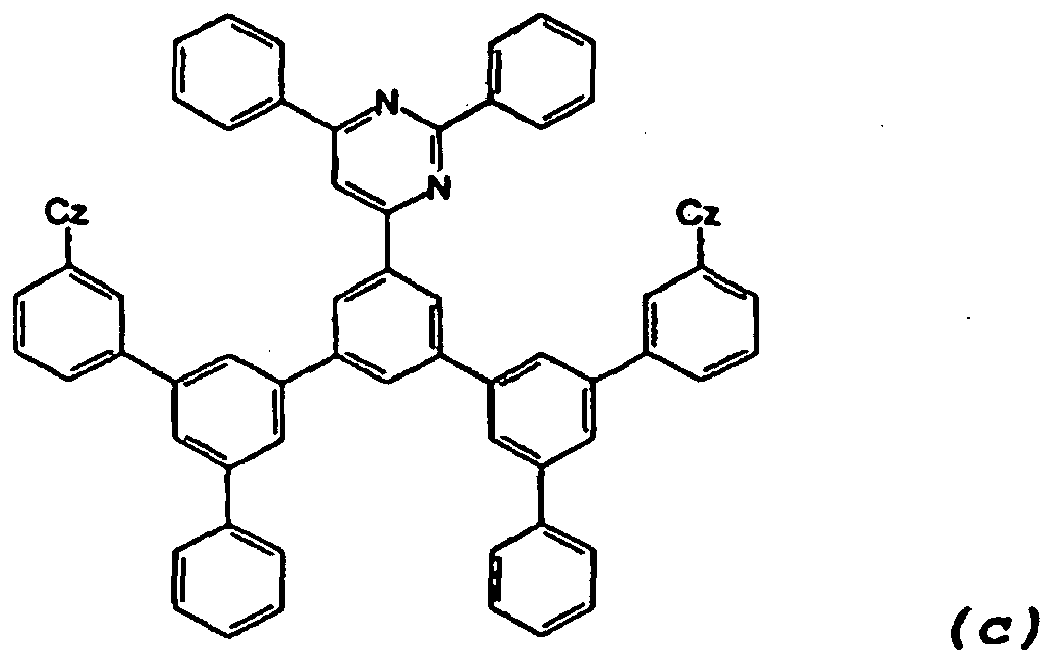 X in Formel (a) jeweils individuell N ist oder zwei X N sind und das Verbleibende CH ist undCz wie oben definiert ist.
 - Organische Verbindung gemäß Anspruch 1, worin der Rest (II) ein Rest der Formel (II-1) ist.
- Organische Verbindung gemäß Anspruch 1, worin die Struktur der Formel (I) durch die Formel (I-1) dargestellt wird:

- Organische Verbindung gemäß Anspruch 1, worin G jeweils eine direkte Verknüpfung oder -(Ph)p- ist, worin Ph Phenylen ist, das einen Substituenten aufweisen kann, und p eine ganze Zahl von 1-8 ist.
- Organische Verbindung gemäß Anspruch 1, worin N-Atome, die nicht miteinander konjugiert sind, nicht mit den Teilstrukturen
-C(G1)=C(G2)-, -C(G3)=N-, -N=N- oder -C≡C-,
verknüpft sind, worin G1, G2 und G3 jeweils unabhängig voneinander H, ein Substituent sind oder einen Teil eines aromatischen Kohlenwasserstoffs oder heterocyclischen Rings bilden. - Organische Verbindung gemäß Anspruch 1, die zwei oder drei Strukturen der Formel (I) umfasst.
- Organische Verbindung gemäß Anspruch 1, die eine Glasübergangstemperatur von ≥ 90°C, eine Verdampfungstemperatur von ≤ 700°C und einen Schmelzpunkt von ≥ 150°C aufweist.
- Organische Verbindung gemäß Anspruch 1, die eine Verbindung der Formel (EM-1) ist:

- Organische Verbindung gemäß Anspruch 1, die eine Verbindung der Formel (EM-2) ist:

- Organische Verbindung gemäß Anspruch 1, die eine Verbindung der Formel (EM-4) ist:

- Organische Verbindung gemäß Anspruch 1, die eine Verbindung der Formel (EM-6) ist:

- Organische Verbindung gemäß Anspruch 1, die eine Verbindung der Formel (EM-7) ist:

- Organische Verbindung gemäß Anspruch 1, die eine Verbindung der Formel (EM-8) ist:

- Organische Verbindung gemäß Anspruch 1, die eine Verbindung der Formel (EM-9) ist:

- Organische Verbindung gemäß Anspruch 1, die eine Verbindung der Formel (EM-10) ist:

- Ladung-transportierendes Material, das eine Verbindung gemäß Anspruch 1 enthält.
- Organische Elektrolumineszenzvorrichtung, die eine Anode, eine Kathode und eine organische lichtemittierende Schicht, die zwischen den beiden Elektroden angeordnet ist, auf einem Substrat umfasst und die eine Schicht aufweist, die eine organische Verbindung gemäß Anspruch 1 enthält.
- Organische Elektrolumineszenzvorrichtung gemäß Anspruch 17, worin die Schicht, die die organische Verbindung gemäß Anspruch 1 enthält, die organische lichtemittierende Schicht ist.
- Organische Elektrolumineszenzvorrichtung gemäß Anspruch 18, worin die organische Verbindung gemäß Anspruch 1 ein Wirtsmaterial der organischen lichtemittierenden Schicht ist und das Wirtsmaterial mit einem organometallischen Komplex dotiert ist.
Applications Claiming Priority (2)
| Application Number | Priority Date | Filing Date | Title |
|---|---|---|---|
| JP2004358592 | 2004-12-10 | ||
| PCT/JP2005/022298 WO2006062062A1 (ja) | 2004-12-10 | 2005-12-05 | 有機化合物、電荷輸送材料および有機電界発光素子 |
Publications (3)
| Publication Number | Publication Date |
|---|---|
| EP1820801A1 EP1820801A1 (de) | 2007-08-22 |
| EP1820801A4 EP1820801A4 (de) | 2009-12-23 |
| EP1820801B1 true EP1820801B1 (de) | 2015-04-01 |
Family
ID=36577889
Family Applications (1)
| Application Number | Title | Priority Date | Filing Date |
|---|---|---|---|
| EP05811601.3A Active EP1820801B1 (de) | 2004-12-10 | 2005-12-05 | Organische verbindung, ladungstransportierendes material und organisches elektrolumineszentes element |
Country Status (6)
| Country | Link |
|---|---|
| US (1) | US8178215B2 (de) |
| EP (1) | EP1820801B1 (de) |
| KR (2) | KR101389735B1 (de) |
| CN (1) | CN101076528B (de) |
| TW (1) | TWI444375B (de) |
| WO (1) | WO2006062062A1 (de) |
Families Citing this family (59)
| Publication number | Priority date | Publication date | Assignee | Title |
|---|---|---|---|---|
| JP5261887B2 (ja) * | 2005-05-17 | 2013-08-14 | 三菱化学株式会社 | モノアミン化合物、電荷輸送材料および有機電界発光素子 |
| US8933622B2 (en) * | 2005-05-24 | 2015-01-13 | Pioneer Corporation | Organic electroluminescence element |
| US8053092B2 (en) | 2005-12-12 | 2011-11-08 | Hodogaya Chemical Co., Ltd. | m-carbazolylphenyl compounds |
| WO2007069740A1 (ja) * | 2005-12-16 | 2007-06-21 | Pioneer Corporation | 有機エレクトロルミネッセンス素子 |
| GB0617167D0 (en) | 2006-08-31 | 2006-10-11 | Cdt Oxford Ltd | Compounds for use in opto-electrical devices |
| JP5167747B2 (ja) * | 2006-10-04 | 2013-03-21 | 三菱化学株式会社 | 低分子塗布型有機電界発光素子用の電荷輸送材料、有機電界発光素子用組成物、有機電界発光素子用薄膜および有機電界発光素子 |
| JP5153127B2 (ja) * | 2006-11-28 | 2013-02-27 | キヤノン株式会社 | アミン化合物及び有機発光素子 |
| KR100850886B1 (ko) * | 2007-09-07 | 2008-08-07 | (주)그라쎌 | 전기발광용 유기금속 화합물 및 이를 발광재료로 채용하고있는 표시소자 |
| JP5499487B2 (ja) * | 2008-02-25 | 2014-05-21 | 三菱化学株式会社 | キノリン系化合物、有機電界発光素子用材料、有機電界発光素子用組成物、有機電界発光素子、有機elディスプレイおよび有機el照明 |
| EP2272828B1 (de) * | 2008-03-24 | 2018-06-27 | Nippon Steel & Sumikin Chemical Co., Ltd. | Organische elektrolumineszenzvorrichtung |
| EP2275458A4 (de) * | 2008-04-24 | 2013-04-17 | Showa Denko Kk | Ladungstransportierende polymerverbindung und organisches elektrolumineszenzelement damit |
| JP5338184B2 (ja) * | 2008-08-06 | 2013-11-13 | コニカミノルタ株式会社 | 有機エレクトロルミネッセンス素子、表示装置、照明装置 |
| KR101288557B1 (ko) * | 2008-12-24 | 2013-07-22 | 제일모직주식회사 | 신규한 유기광전소자용 화합물 및 이를 포함하는 유기광전소자 |
| US8691399B2 (en) * | 2009-01-08 | 2014-04-08 | General Electric Company | Electron-transporting materials and processes for making the same |
| US7989476B2 (en) | 2009-01-08 | 2011-08-02 | General Electric Company | Electron-transporting materials and processes for making the same |
| US8709615B2 (en) | 2011-07-28 | 2014-04-29 | Universal Display Corporation | Heteroleptic iridium complexes as dopants |
| US11910700B2 (en) | 2009-03-23 | 2024-02-20 | Universal Display Corporation | Heteroleptic iridium complexes as dopants |
| US8722205B2 (en) | 2009-03-23 | 2014-05-13 | Universal Display Corporation | Heteroleptic iridium complex |
| US20110177622A1 (en) * | 2009-12-28 | 2011-07-21 | Global Solar Energy, Inc. | Apparatus and methods of mixing and depositing thin film photovoltaic compositions |
| JP5560592B2 (ja) * | 2009-05-29 | 2014-07-30 | 三菱化学株式会社 | 含窒素複素環化合物、有機電界発光素子材料、有機電界発光素子用組成物、有機電界発光素子、有機elディスプレイ及び有機el照明 |
| US8617720B2 (en) | 2009-12-21 | 2013-12-31 | E I Du Pont De Nemours And Company | Electroactive composition and electronic device made with the composition |
| JP5584702B2 (ja) * | 2009-12-28 | 2014-09-03 | 新日鉄住金化学株式会社 | 有機電界発光素子 |
| WO2011108707A1 (ja) * | 2010-03-05 | 2011-09-09 | 出光興産株式会社 | 有機エレクトロルミネッセンス素子用材料及びそれを用いた有機エレクトロルミネッセンス素子 |
| JP2012033918A (ja) | 2010-07-08 | 2012-02-16 | Mitsubishi Chemicals Corp | 有機電界発光素子、有機電界発光デバイス、有機el表示装置及び有機el照明 |
| DE102010027218A1 (de) | 2010-07-15 | 2012-01-19 | Merck Patent Gmbh | Organische Komplexe enthaltend Metalle |
| EP2638579B1 (de) * | 2010-11-09 | 2018-01-24 | Koninklijke Philips N.V. | Organisches elektrolumineszenzelement |
| WO2012078005A2 (ko) * | 2010-12-10 | 2012-06-14 | 고려대학교 산학협력단 | 정공전도성을 갖는 화합물, 이를 포함하는 정공전도특성을 갖는 공흡착체, 및 이를 포함하는 염료감응 태양전지 |
| EP2662368A4 (de) | 2010-12-20 | 2014-06-25 | Idemitsu Kosan Co | Aromatisches heterocyclisches derivat und organisches elektrolumineszenzelement damit |
| KR20130130788A (ko) * | 2010-12-20 | 2013-12-02 | 이 아이 듀폰 디 네모아 앤드 캄파니 | 전자적 응용을 위한 트라이아진 유도체 |
| CN103459375B (zh) * | 2011-04-07 | 2016-10-12 | 三菱化学株式会社 | 有机化合物、电荷传输材料、含有该化合物的组合物、有机场致发光元件、显示装置及照明装置 |
| KR20140094520A (ko) * | 2011-10-26 | 2014-07-30 | 이데미쓰 고산 가부시키가이샤 | 유기 일렉트로 루미네선스 소자 및 유기 일렉트로 루미네선스 소자용 재료 |
| CN102503937B (zh) * | 2011-11-18 | 2014-09-10 | 华南理工大学 | 含有吡啶和咔唑的双极性有机材料及其制备方法和应用 |
| KR102261235B1 (ko) | 2011-11-22 | 2021-06-04 | 이데미쓰 고산 가부시키가이샤 | 방향족 복소 고리 유도체, 유기 일렉트로루미네선스 소자용 재료 및 유기 일렉트로루미네선스 소자 |
| JP5684206B2 (ja) * | 2012-09-14 | 2015-03-11 | 株式会社東芝 | 有機電界発光素子 |
| EP2922932B1 (de) * | 2012-11-23 | 2019-06-12 | Merck Patent GmbH | Materialien für elektronische vorrichtungen |
| KR101593182B1 (ko) | 2012-12-12 | 2016-02-19 | 삼성전자 주식회사 | 유기광전자소자용 화합물, 이를 포함하는 유기발광소자 및 상기 유기발광소자를 포함하는 표시장치 |
| JP6182217B2 (ja) | 2013-11-13 | 2017-08-16 | 出光興産株式会社 | 化合物、有機エレクトロルミネッセンス素子用材料、有機エレクトロルミネッセンス素子および電子機器 |
| CN104370887B (zh) * | 2013-12-26 | 2016-08-24 | 北京阿格蕾雅科技发展有限公司 | 2,6-双[3-(n-咔唑基)苯基]吡啶类化合物的合成方法 |
| JP6501771B2 (ja) * | 2014-06-11 | 2019-04-17 | 保土谷化学工業株式会社 | ピリミジン誘導体および有機エレクトロルミネッセンス素子 |
| JP6500644B2 (ja) * | 2014-07-01 | 2019-04-17 | 東ソー株式会社 | トリアジン化合物、その製造方法、及びその用途 |
| JP6421502B2 (ja) * | 2014-09-02 | 2018-11-14 | 東ソー株式会社 | トリアジン化合物、その製造方法、及びそれを構成成分とする有機電界発光素子 |
| CN106573912A (zh) * | 2014-07-01 | 2017-04-19 | 东曹株式会社 | 三嗪化合物、其制造方法、及其用途 |
| CN105646459A (zh) * | 2014-11-13 | 2016-06-08 | 上海和辉光电有限公司 | 一种化合物及其制备方法和应用 |
| JP6640735B2 (ja) | 2014-11-28 | 2020-02-05 | 出光興産株式会社 | 化合物、有機エレクトロルミネッセンス素子用材料、有機エレクトロルミネッセンス素子および電子機器 |
| EP3353844B1 (de) | 2015-03-27 | 2022-05-11 | Mason K. Harrup | Vollständig anorganische lösungsmittel für elektrolyte |
| JP6764671B2 (ja) * | 2015-04-14 | 2020-10-07 | 株式会社半導体エネルギー研究所 | 複素環化合物、発光素子、発光装置、電子機器、および照明装置 |
| US10153437B2 (en) | 2015-05-12 | 2018-12-11 | Semiconductor Energy Laboratory Co., Ltd. | Compound, light-emitting element, light-emitting device, electronic device, and lighting device |
| KR102491790B1 (ko) * | 2015-09-25 | 2023-01-26 | 엘지디스플레이 주식회사 | 유기전계발광소자 |
| US20170104172A1 (en) * | 2015-10-12 | 2017-04-13 | The Regents Of The University Of Michigan | Organic Light Emitting Diode Having a Mixed Blocking Layer |
| JP6789195B2 (ja) * | 2016-08-24 | 2020-11-25 | サイノラ ゲゼルシャフト ミット ベシュレンクテル ハフツング | 特に有機光電子デバイスに使用するための有機分子 |
| US10707531B1 (en) | 2016-09-27 | 2020-07-07 | New Dominion Enterprises Inc. | All-inorganic solvents for electrolytes |
| JP6950710B2 (ja) * | 2017-01-23 | 2021-10-13 | 三菱ケミカル株式会社 | 発光層形成用組成物及び該発光層形成用組成物を含有する有機電界発光素子 |
| WO2018145995A2 (de) * | 2017-02-07 | 2018-08-16 | Cynora Gmbh | Organische moleküle, insbesondere zur verwendung in organischen optoelektronischen vorrichtungen |
| US11581487B2 (en) | 2017-04-26 | 2023-02-14 | Oti Lumionics Inc. | Patterned conductive coating for surface of an opto-electronic device |
| KR102487503B1 (ko) * | 2017-07-04 | 2023-01-12 | 솔루스첨단소재 주식회사 | 유기 화합물 및 이를 이용한 유기 전계 발광 소자 |
| US11706977B2 (en) | 2018-01-11 | 2023-07-18 | Samsung Electronics Co., Ltd. | Heterocyclic compound, composition including the same, and organic light-emitting device including the heterocyclic compound |
| US11751415B2 (en) | 2018-02-02 | 2023-09-05 | Oti Lumionics Inc. | Materials for forming a nucleation-inhibiting coating and devices incorporating same |
| KR102637792B1 (ko) * | 2018-03-22 | 2024-02-19 | 삼성디스플레이 주식회사 | 유기 발광 소자 및 이를 포함한 전자 장치 |
| CN113785411B (zh) | 2019-03-07 | 2023-04-11 | Oti照明公司 | 用于形成成核抑制涂层的材料和结合所述成核抑制涂层的装置 |
Citations (1)
| Publication number | Priority date | Publication date | Assignee | Title |
|---|---|---|---|---|
| WO2005057987A1 (ja) * | 2003-12-15 | 2005-06-23 | Idemitsu Kosan Co., Ltd. | 有機エレクトロルミネッセンス素子用材料及びそれを用いた有機エレクトロルミネッセンス素子 |
Family Cites Families (57)
| Publication number | Priority date | Publication date | Assignee | Title |
|---|---|---|---|---|
| US4539507A (en) | 1983-03-25 | 1985-09-03 | Eastman Kodak Company | Organic electroluminescent devices having improved power conversion efficiencies |
| US4720432A (en) | 1987-02-11 | 1988-01-19 | Eastman Kodak Company | Electroluminescent device with organic luminescent medium |
| CS262585B1 (cs) | 1987-12-17 | 1989-03-14 | Urst Antonin Doc Ing Csc Kurf | Luminofomí bis(4,6 diarylpyridin-2yl)-areny a způsob jejich přípravy |
| US4826978A (en) | 1987-12-29 | 1989-05-02 | Milliken Research Corporation | Reactive, non-yellowing triazine compounds useful as UV screening agents for polymers |
| JPH07119407B2 (ja) | 1989-03-20 | 1995-12-20 | 出光興産株式会社 | エレクトロルミネッセンス素子 |
| JPH0348666A (ja) | 1989-07-17 | 1991-03-01 | Rasa Kogyo Kk | 芳香族ジアミン化合物の製造方法 |
| US5061569A (en) | 1990-07-26 | 1991-10-29 | Eastman Kodak Company | Electroluminescent device with organic electroluminescent medium |
| EP0497734B1 (de) | 1991-01-31 | 2000-05-10 | Ciba SC Holding AG | Verfahren zur Herstellung von 2-(2',4'-Dihydroxyphenyl)-4,6-diaryl-s-triazinen |
| JP3016896B2 (ja) | 1991-04-08 | 2000-03-06 | パイオニア株式会社 | 有機エレクトロルミネッセンス素子 |
| JPH07110940B2 (ja) | 1991-06-05 | 1995-11-29 | 住友化学工業株式会社 | 有機エレクトロルミネッセンス素子 |
| DE69204359T2 (de) | 1991-06-05 | 1996-04-18 | Sumitomo Chemical Co | Organische elektroluminescente Vorrichtungen. |
| JP2690814B2 (ja) | 1991-09-03 | 1997-12-17 | 山之内製薬株式会社 | ピラゾロトリアゾール誘導体 |
| JP3562652B2 (ja) | 1992-04-03 | 2004-09-08 | パイオニア株式会社 | 有機エレクトロルミネッセンス素子 |
| JP3098330B2 (ja) | 1992-08-11 | 2000-10-16 | 出光興産株式会社 | ピラジン誘導体及びその製造法 |
| JPH06207169A (ja) | 1992-11-17 | 1994-07-26 | Idemitsu Kosan Co Ltd | 有機エレクトロルミネッセンス素子 |
| JP3071091B2 (ja) | 1993-03-17 | 2000-07-31 | 三洋電機株式会社 | 電界発光素子 |
| JPH0753953A (ja) | 1993-08-19 | 1995-02-28 | Mitsubishi Chem Corp | 有機電界発光素子 |
| TW254936B (de) | 1993-10-22 | 1995-08-21 | Ciba Geigy | |
| US5726310A (en) | 1995-12-14 | 1998-03-10 | Ciba Specialty Chemicals Corporation | Process for the preparation of 2-(2,4-dihydroxylphenyl)-4,6-bis(2,4-dimehylphenyl)-s-triazine |
| WO1997033193A2 (en) | 1996-02-23 | 1997-09-12 | The Dow Chemical Company | Cross-linkable or chain extendable polyarylpolyamines and films thereof |
| DE19627069A1 (de) | 1996-07-05 | 1998-01-08 | Bayer Ag | Elektrolumineszierende Anordnungen unter Verwendung von lamellaren Elektroden |
| US5776622A (en) | 1996-07-29 | 1998-07-07 | Eastman Kodak Company | Bilayer eletron-injeting electrode for use in an electroluminescent device |
| US5645948A (en) | 1996-08-20 | 1997-07-08 | Eastman Kodak Company | Blue organic electroluminescent devices |
| JPH10270171A (ja) | 1997-01-27 | 1998-10-09 | Junji Kido | 有機エレクトロルミネッセント素子 |
| US6303238B1 (en) | 1997-12-01 | 2001-10-16 | The Trustees Of Princeton University | OLEDs doped with phosphorescent compounds |
| JP3750315B2 (ja) | 1997-10-27 | 2006-03-01 | 三菱化学株式会社 | 有機電界発光素子 |
| JPH11251067A (ja) | 1998-03-02 | 1999-09-17 | Junji Kido | 有機エレクトロルミネッセント素子 |
| JP3748491B2 (ja) | 1998-03-27 | 2006-02-22 | 出光興産株式会社 | 有機エレクトロルミネッセンス素子 |
| JP4058842B2 (ja) | 1998-05-13 | 2008-03-12 | 三菱化学株式会社 | 有機電界発光素子 |
| EP1108706B1 (de) | 1998-08-27 | 2005-07-20 | Japan Science and Technology Agency | Katalytische herstellung von aldehyden durch direkte hydrierung von carbonsäuren |
| JP2000150168A (ja) | 1998-11-13 | 2000-05-30 | Toppan Printing Co Ltd | 耐熱性低抵抗正孔輸送材料および有機薄膜発光素子 |
| JP2000159221A (ja) | 1998-11-25 | 2000-06-13 | Kanebo Ltd | 一個箱 |
| JP4320811B2 (ja) | 1998-12-07 | 2009-08-26 | コニカミノルタホールディングス株式会社 | 有機エレクトロルミネッセンス素子 |
| JP4006862B2 (ja) | 1998-12-22 | 2007-11-14 | コニカミノルタホールディングス株式会社 | 新規アミノ化合物とその製造方法、及び用途 |
| ATE344532T1 (de) | 1999-05-13 | 2006-11-15 | Univ Princeton | Lichtemittierende, organische, auf elektrophosphoreszenz basierende anordnung mit sehr hoher quantenausbeute |
| JP2001223084A (ja) | 2000-02-07 | 2001-08-17 | Junji Kido | 有機電界発光素子 |
| JP4890669B2 (ja) | 2000-03-13 | 2012-03-07 | Tdk株式会社 | 有機el素子 |
| DE10032254B4 (de) | 2000-07-03 | 2006-05-04 | Forschungszentrum Jülich GmbH | Nukleotidsequenz kodierend für eine Benzaldehyd-Lyase und Verfahren zur stereoselektiven Synthese von (R)-2-Hydroxyketonen |
| JP2002100482A (ja) | 2000-09-20 | 2002-04-05 | Mitsubishi Chemicals Corp | 有機電界発光素子 |
| JP2002100478A (ja) | 2000-09-20 | 2002-04-05 | Mitsubishi Chemicals Corp | 有機電界発光素子及びその製造方法 |
| JP2003022893A (ja) | 2001-07-06 | 2003-01-24 | Fuji Photo Film Co Ltd | 発光素子 |
| WO2003078541A1 (en) | 2002-03-15 | 2003-09-25 | Idemitsu Kosan Co., Ltd. | Material for organic electroluminescent devices and organic electroluminescent devices made by using the same |
| JP4316387B2 (ja) | 2002-03-22 | 2009-08-19 | 出光興産株式会社 | 有機エレクトロルミネッセンス素子用材料及びそれを用いた有機エレクトロルミネッセンス素子 |
| KR20040094866A (ko) * | 2002-03-25 | 2004-11-10 | 이데미쓰 고산 가부시키가이샤 | 유기 전자발광 소자용 재료 및 이를 이용한 유기 전자발광소자 |
| JP4103491B2 (ja) * | 2002-08-07 | 2008-06-18 | コニカミノルタホールディングス株式会社 | 有機エレクトロルミネッセンス素子及び表示装置 |
| JP4427947B2 (ja) | 2002-11-18 | 2010-03-10 | コニカミノルタホールディングス株式会社 | 有機エレクトロルミネッセンス素子及び表示装置 |
| JP4707082B2 (ja) * | 2002-11-26 | 2011-06-22 | コニカミノルタホールディングス株式会社 | 有機エレクトロルミネッセンス素子および表示装置 |
| JP2004311413A (ja) * | 2003-03-26 | 2004-11-04 | Konica Minolta Holdings Inc | 有機エレクトロルミネッセンス素子、表示装置及び照明装置 |
| EP2592905B1 (de) * | 2003-07-31 | 2014-11-12 | Mitsubishi Chemical Corporation | Verbindung, Ladungstransportmaterial und organisches Elektrolumineszenzelement |
| JP4325324B2 (ja) * | 2003-09-10 | 2009-09-02 | コニカミノルタホールディングス株式会社 | 有機エレクトロルミネッセンス素子 |
| TWI428053B (zh) * | 2004-02-09 | 2014-02-21 | Idemitsu Kosan Co | Organic electroluminescent element |
| TW200541401A (en) * | 2004-02-13 | 2005-12-16 | Idemitsu Kosan Co | Organic electroluminescent device |
| JPWO2005085387A1 (ja) | 2004-03-08 | 2007-12-13 | 出光興産株式会社 | 有機エレクトロルミネッセンス素子用材料及びそれを利用した有機エレクトロルミネッセンス素子 |
| WO2006067976A1 (ja) * | 2004-12-24 | 2006-06-29 | Pioneer Corporation | 有機化合物、電荷輸送材料および有機電界発光素子 |
| US9365767B2 (en) * | 2005-02-21 | 2016-06-14 | Mitsubishi Chemical Corporation | Organic electric field light emitting element and production therefor |
| JP5261887B2 (ja) * | 2005-05-17 | 2013-08-14 | 三菱化学株式会社 | モノアミン化合物、電荷輸送材料および有機電界発光素子 |
| US8933622B2 (en) * | 2005-05-24 | 2015-01-13 | Pioneer Corporation | Organic electroluminescence element |
-
2005
- 2005-12-05 EP EP05811601.3A patent/EP1820801B1/de active Active
- 2005-12-05 WO PCT/JP2005/022298 patent/WO2006062062A1/ja active Application Filing
- 2005-12-05 KR KR1020077013039A patent/KR101389735B1/ko active IP Right Grant
- 2005-12-05 CN CN2005800424188A patent/CN101076528B/zh active Active
- 2005-12-05 US US11/721,401 patent/US8178215B2/en active Active
- 2005-12-05 KR KR1020127015673A patent/KR101388472B1/ko active IP Right Grant
- 2005-12-09 TW TW094143665A patent/TWI444375B/zh active
Patent Citations (2)
| Publication number | Priority date | Publication date | Assignee | Title |
|---|---|---|---|---|
| WO2005057987A1 (ja) * | 2003-12-15 | 2005-06-23 | Idemitsu Kosan Co., Ltd. | 有機エレクトロルミネッセンス素子用材料及びそれを用いた有機エレクトロルミネッセンス素子 |
| EP1696708A1 (de) * | 2003-12-15 | 2006-08-30 | Idemitsu Kosan Co., Ltd. | Stoff für organische elektrolumineszenzvorrichtung und darauf basierende organische elektrolumineszenzvorrichtung |
Also Published As
| Publication number | Publication date |
|---|---|
| EP1820801A4 (de) | 2009-12-23 |
| KR101389735B1 (ko) | 2014-04-29 |
| KR20070085974A (ko) | 2007-08-27 |
| KR20120085912A (ko) | 2012-08-01 |
| CN101076528A (zh) | 2007-11-21 |
| KR101388472B1 (ko) | 2014-04-23 |
| US8178215B2 (en) | 2012-05-15 |
| CN101076528B (zh) | 2012-06-20 |
| TWI444375B (zh) | 2014-07-11 |
| TW200631950A (en) | 2006-09-16 |
| WO2006062062A1 (ja) | 2006-06-15 |
| US20090236973A1 (en) | 2009-09-24 |
| EP1820801A1 (de) | 2007-08-22 |
Similar Documents
| Publication | Publication Date | Title |
|---|---|---|
| EP1820801B1 (de) | Organische verbindung, ladungstransportierendes material und organisches elektrolumineszentes element | |
| JP5050344B2 (ja) | 有機化合物、電荷輸送材料および有機電界発光素子 | |
| JP5082230B2 (ja) | 有機化合物、電荷輸送材料および有機電界発光素子 | |
| EP1672961B1 (de) | Zusammengesetztes ladungstransportmaterial und organisches elektrolumineszenzbauelement | |
| KR101593326B1 (ko) | 벤조플루오렌 화합물, 그 화합물을 이용한 발광층용 재료 및 유기 전계 발광 소자 | |
| JP4561221B2 (ja) | 化合物、電荷輸送材料および有機電界発光素子 | |
| KR101199276B1 (ko) | 유기 화합물, 전하 수송 재료, 및 유기 전계 발광 소자 | |
| KR101395615B1 (ko) | 유기 화합물, 전하 수송 재료, 전하 수송 재료용 조성물 및유기 전계 발광 소자 | |
| JP5098177B2 (ja) | 有機化合物、電荷輸送材料及び有機電界発光素子 | |
| WO2006123667A1 (ja) | モノアミン化合物、電荷輸送材料および有機電界発光素子 | |
| JP4622433B2 (ja) | 化合物、電子輸送材料および有機電界発光素子 | |
| KR20110116184A (ko) | 피리딜기가 연결된 트리아졸환 구조를 갖는 화합물 및 유기 전계 발광 소자 | |
| KR101026913B1 (ko) | 유기 전계발광 소자 | |
| WO2017086225A1 (ja) | イリジウム錯体ならびに該化合物を用いた発光材料および有機発光素子 |
Legal Events
| Date | Code | Title | Description |
|---|---|---|---|
| PUAI | Public reference made under article 153(3) epc to a published international application that has entered the european phase |
Free format text: ORIGINAL CODE: 0009012 |
|
| 17P | Request for examination filed |
Effective date: 20070606 |
|
| AK | Designated contracting states |
Kind code of ref document: A1 Designated state(s): DE |
|
| DAX | Request for extension of the european patent (deleted) | ||
| RBV | Designated contracting states (corrected) |
Designated state(s): DE |
|
| A4 | Supplementary search report drawn up and despatched |
Effective date: 20091120 |
|
| RIC1 | Information provided on ipc code assigned before grant |
Ipc: C07D 403/14 20060101ALI20091116BHEP Ipc: C07D 401/14 20060101AFI20070719BHEP Ipc: C09K 11/06 20060101ALI20091116BHEP Ipc: H01L 51/50 20060101ALI20091116BHEP |
|
| 17Q | First examination report despatched |
Effective date: 20100528 |
|
| RAP1 | Party data changed (applicant data changed or rights of an application transferred) |
Owner name: MITSUBISHI CHEMICAL CORPORATION Owner name: PIONEER CORPORATION |
|
| RAP1 | Party data changed (applicant data changed or rights of an application transferred) |
Owner name: PIONEER CORPORATION Owner name: MITSUBISHI CHEMICAL CORPORATION |
|
| GRAP | Despatch of communication of intention to grant a patent |
Free format text: ORIGINAL CODE: EPIDOSNIGR1 |
|
| INTG | Intention to grant announced |
Effective date: 20141112 |
|
| GRAS | Grant fee paid |
Free format text: ORIGINAL CODE: EPIDOSNIGR3 |
|
| GRAA | (expected) grant |
Free format text: ORIGINAL CODE: 0009210 |
|
| AK | Designated contracting states |
Kind code of ref document: B1 Designated state(s): DE |
|
| REG | Reference to a national code |
Ref country code: DE Ref legal event code: R081 Ref document number: 602005046213 Country of ref document: DE Owner name: PIONEER CORPORATION, KAWASAKI-SHI, JP Free format text: FORMER OWNERS: MITSUBISHI CHEMICAL CORP., TOKIO/TOKYO, JP; PIONEER CORPORATION, TOKYO, JP Ref country code: DE Ref legal event code: R081 Ref document number: 602005046213 Country of ref document: DE Owner name: MITSUBISHI CHEMICAL CORPORATION, JP Free format text: FORMER OWNERS: MITSUBISHI CHEMICAL CORP., TOKIO/TOKYO, JP; PIONEER CORPORATION, TOKYO, JP |
|
| REG | Reference to a national code |
Ref country code: DE Ref legal event code: R096 Ref document number: 602005046213 Country of ref document: DE Effective date: 20150513 |
|
| REG | Reference to a national code |
Ref country code: DE Ref legal event code: R097 Ref document number: 602005046213 Country of ref document: DE |
|
| PLBE | No opposition filed within time limit |
Free format text: ORIGINAL CODE: 0009261 |
|
| STAA | Information on the status of an ep patent application or granted ep patent |
Free format text: STATUS: NO OPPOSITION FILED WITHIN TIME LIMIT |
|
| 26N | No opposition filed |
Effective date: 20160105 |
|
| REG | Reference to a national code |
Ref country code: DE Ref legal event code: R082 Ref document number: 602005046213 Country of ref document: DE Representative=s name: HOFFMANN - EITLE PATENT- UND RECHTSANWAELTE PA, DE Ref country code: DE Ref legal event code: R081 Ref document number: 602005046213 Country of ref document: DE Owner name: PIONEER CORPORATION, KAWASAKI-SHI, JP Free format text: FORMER OWNERS: MITSUBISHI CHEMICAL CORPORATION, TOKIO, JP; PIONEER CORPORATION, KAWASAKI-SHI, KANAGAWA, JP Ref country code: DE Ref legal event code: R081 Ref document number: 602005046213 Country of ref document: DE Owner name: MITSUBISHI CHEMICAL CORPORATION, JP Free format text: FORMER OWNERS: MITSUBISHI CHEMICAL CORPORATION, TOKIO, JP; PIONEER CORPORATION, KAWASAKI-SHI, KANAGAWA, JP |
|
| P01 | Opt-out of the competence of the unified patent court (upc) registered |
Effective date: 20230522 |
|
| PGFP | Annual fee paid to national office [announced via postgrant information from national office to epo] |
Ref country code: DE Payment date: 20231031 Year of fee payment: 19 |