EP1612860A2 - Interposeur, son procédé de fabrication, et dispositif semi-conducteur l'utilisant - Google Patents
Interposeur, son procédé de fabrication, et dispositif semi-conducteur l'utilisant Download PDFInfo
- Publication number
- EP1612860A2 EP1612860A2 EP05253670A EP05253670A EP1612860A2 EP 1612860 A2 EP1612860 A2 EP 1612860A2 EP 05253670 A EP05253670 A EP 05253670A EP 05253670 A EP05253670 A EP 05253670A EP 1612860 A2 EP1612860 A2 EP 1612860A2
- Authority
- EP
- European Patent Office
- Prior art keywords
- interposer
- portions
- forming
- holes
- wiring patterns
- Prior art date
- Legal status (The legal status is an assumption and is not a legal conclusion. Google has not performed a legal analysis and makes no representation as to the accuracy of the status listed.)
- Granted
Links
- 239000004065 semiconductor Substances 0.000 title claims abstract description 61
- 238000004519 manufacturing process Methods 0.000 title claims description 17
- 229910052751 metal Inorganic materials 0.000 claims abstract description 34
- 239000002184 metal Substances 0.000 claims abstract description 34
- 239000012212 insulator Substances 0.000 claims abstract description 25
- 229920005989 resin Polymers 0.000 claims abstract description 16
- 239000011347 resin Substances 0.000 claims abstract description 16
- 238000004806 packaging method and process Methods 0.000 claims abstract description 8
- 239000004020 conductor Substances 0.000 claims description 16
- 230000001681 protective effect Effects 0.000 claims description 14
- 238000005520 cutting process Methods 0.000 claims description 6
- 239000000919 ceramic Substances 0.000 claims description 2
- 238000010304 firing Methods 0.000 claims description 2
- 238000000034 method Methods 0.000 description 33
- 239000010949 copper Substances 0.000 description 31
- 229910000679 solder Inorganic materials 0.000 description 24
- 239000010931 gold Substances 0.000 description 17
- PXHVJJICTQNCMI-UHFFFAOYSA-N Nickel Chemical compound [Ni] PXHVJJICTQNCMI-UHFFFAOYSA-N 0.000 description 16
- 230000015572 biosynthetic process Effects 0.000 description 13
- 238000012545 processing Methods 0.000 description 12
- 238000007641 inkjet printing Methods 0.000 description 10
- 239000003822 epoxy resin Substances 0.000 description 9
- 239000000463 material Substances 0.000 description 9
- 229920000647 polyepoxide Polymers 0.000 description 9
- 239000000654 additive Substances 0.000 description 7
- RYGMFSIKBFXOCR-UHFFFAOYSA-N Copper Chemical compound [Cu] RYGMFSIKBFXOCR-UHFFFAOYSA-N 0.000 description 5
- 229910052802 copper Inorganic materials 0.000 description 5
- 238000007747 plating Methods 0.000 description 5
- 238000007650 screen-printing Methods 0.000 description 5
- 238000001039 wet etching Methods 0.000 description 5
- XUIMIQQOPSSXEZ-UHFFFAOYSA-N Silicon Chemical compound [Si] XUIMIQQOPSSXEZ-UHFFFAOYSA-N 0.000 description 4
- 239000003795 chemical substances by application Substances 0.000 description 4
- 238000007772 electroless plating Methods 0.000 description 4
- 229920001721 polyimide Polymers 0.000 description 4
- 239000009719 polyimide resin Substances 0.000 description 4
- 229910052710 silicon Inorganic materials 0.000 description 4
- 239000010703 silicon Substances 0.000 description 4
- 238000004544 sputter deposition Methods 0.000 description 4
- VYPSYNLAJGMNEJ-UHFFFAOYSA-N Silicium dioxide Chemical compound O=[Si]=O VYPSYNLAJGMNEJ-UHFFFAOYSA-N 0.000 description 3
- 238000003475 lamination Methods 0.000 description 3
- 229920001187 thermosetting polymer Polymers 0.000 description 3
- 229910052782 aluminium Inorganic materials 0.000 description 2
- XAGFODPZIPBFFR-UHFFFAOYSA-N aluminium Chemical compound [Al] XAGFODPZIPBFFR-UHFFFAOYSA-N 0.000 description 2
- 238000005516 engineering process Methods 0.000 description 2
- PCHJSUWPFVWCPO-UHFFFAOYSA-N gold Chemical compound [Au] PCHJSUWPFVWCPO-UHFFFAOYSA-N 0.000 description 2
- 229910052737 gold Inorganic materials 0.000 description 2
- 238000001020 plasma etching Methods 0.000 description 2
- 238000007740 vapor deposition Methods 0.000 description 2
- 239000003990 capacitor Substances 0.000 description 1
- 229910052681 coesite Inorganic materials 0.000 description 1
- 239000000470 constituent Substances 0.000 description 1
- 229910052906 cristobalite Inorganic materials 0.000 description 1
- 238000001312 dry etching Methods 0.000 description 1
- 238000001652 electrophoretic deposition Methods 0.000 description 1
- 239000002241 glass-ceramic Substances 0.000 description 1
- 238000007731 hot pressing Methods 0.000 description 1
- 229910052759 nickel Inorganic materials 0.000 description 1
- 230000003647 oxidation Effects 0.000 description 1
- 238000007254 oxidation reaction Methods 0.000 description 1
- 238000000926 separation method Methods 0.000 description 1
- 239000000377 silicon dioxide Substances 0.000 description 1
- 229910052814 silicon oxide Inorganic materials 0.000 description 1
- 238000000992 sputter etching Methods 0.000 description 1
- 229910052682 stishovite Inorganic materials 0.000 description 1
- 229910052905 tridymite Inorganic materials 0.000 description 1
Images


Classifications
-
- H—ELECTRICITY
- H01—ELECTRIC ELEMENTS
- H01L—SEMICONDUCTOR DEVICES NOT COVERED BY CLASS H10
- H01L23/00—Details of semiconductor or other solid state devices
- H01L23/12—Mountings, e.g. non-detachable insulating substrates
- H01L23/14—Mountings, e.g. non-detachable insulating substrates characterised by the material or its electrical properties
- H01L23/147—Semiconductor insulating substrates
-
- H—ELECTRICITY
- H01—ELECTRIC ELEMENTS
- H01L—SEMICONDUCTOR DEVICES NOT COVERED BY CLASS H10
- H01L23/00—Details of semiconductor or other solid state devices
- H01L23/12—Mountings, e.g. non-detachable insulating substrates
- H01L23/14—Mountings, e.g. non-detachable insulating substrates characterised by the material or its electrical properties
-
- H—ELECTRICITY
- H01—ELECTRIC ELEMENTS
- H01L—SEMICONDUCTOR DEVICES NOT COVERED BY CLASS H10
- H01L23/00—Details of semiconductor or other solid state devices
- H01L23/48—Arrangements for conducting electric current to or from the solid state body in operation, e.g. leads, terminal arrangements ; Selection of materials therefor
- H01L23/488—Arrangements for conducting electric current to or from the solid state body in operation, e.g. leads, terminal arrangements ; Selection of materials therefor consisting of soldered or bonded constructions
- H01L23/498—Leads, i.e. metallisations or lead-frames on insulating substrates, e.g. chip carriers
- H01L23/49827—Via connections through the substrates, e.g. pins going through the substrate, coaxial cables
-
- H—ELECTRICITY
- H01—ELECTRIC ELEMENTS
- H01L—SEMICONDUCTOR DEVICES NOT COVERED BY CLASS H10
- H01L25/00—Assemblies consisting of a plurality of individual semiconductor or other solid state devices ; Multistep manufacturing processes thereof
- H01L25/03—Assemblies consisting of a plurality of individual semiconductor or other solid state devices ; Multistep manufacturing processes thereof all the devices being of a type provided for in the same subgroup of groups H01L27/00 - H01L33/00, or in a single subclass of H10K, H10N, e.g. assemblies of rectifier diodes
- H01L25/04—Assemblies consisting of a plurality of individual semiconductor or other solid state devices ; Multistep manufacturing processes thereof all the devices being of a type provided for in the same subgroup of groups H01L27/00 - H01L33/00, or in a single subclass of H10K, H10N, e.g. assemblies of rectifier diodes the devices not having separate containers
- H01L25/065—Assemblies consisting of a plurality of individual semiconductor or other solid state devices ; Multistep manufacturing processes thereof all the devices being of a type provided for in the same subgroup of groups H01L27/00 - H01L33/00, or in a single subclass of H10K, H10N, e.g. assemblies of rectifier diodes the devices not having separate containers the devices being of a type provided for in group H01L27/00
- H01L25/0657—Stacked arrangements of devices
-
- H—ELECTRICITY
- H01—ELECTRIC ELEMENTS
- H01L—SEMICONDUCTOR DEVICES NOT COVERED BY CLASS H10
- H01L21/00—Processes or apparatus adapted for the manufacture or treatment of semiconductor or solid state devices or of parts thereof
- H01L21/67—Apparatus specially adapted for handling semiconductor or electric solid state devices during manufacture or treatment thereof; Apparatus specially adapted for handling wafers during manufacture or treatment of semiconductor or electric solid state devices or components ; Apparatus not specifically provided for elsewhere
- H01L21/683—Apparatus specially adapted for handling semiconductor or electric solid state devices during manufacture or treatment thereof; Apparatus specially adapted for handling wafers during manufacture or treatment of semiconductor or electric solid state devices or components ; Apparatus not specifically provided for elsewhere for supporting or gripping
- H01L21/6835—Apparatus specially adapted for handling semiconductor or electric solid state devices during manufacture or treatment thereof; Apparatus specially adapted for handling wafers during manufacture or treatment of semiconductor or electric solid state devices or components ; Apparatus not specifically provided for elsewhere for supporting or gripping using temporarily an auxiliary support
-
- H—ELECTRICITY
- H01—ELECTRIC ELEMENTS
- H01L—SEMICONDUCTOR DEVICES NOT COVERED BY CLASS H10
- H01L2224/00—Indexing scheme for arrangements for connecting or disconnecting semiconductor or solid-state bodies and methods related thereto as covered by H01L24/00
- H01L2224/01—Means for bonding being attached to, or being formed on, the surface to be connected, e.g. chip-to-package, die-attach, "first-level" interconnects; Manufacturing methods related thereto
- H01L2224/10—Bump connectors; Manufacturing methods related thereto
- H01L2224/15—Structure, shape, material or disposition of the bump connectors after the connecting process
- H01L2224/16—Structure, shape, material or disposition of the bump connectors after the connecting process of an individual bump connector
- H01L2224/161—Disposition
- H01L2224/16151—Disposition the bump connector connecting between a semiconductor or solid-state body and an item not being a semiconductor or solid-state body, e.g. chip-to-substrate, chip-to-passive
- H01L2224/16221—Disposition the bump connector connecting between a semiconductor or solid-state body and an item not being a semiconductor or solid-state body, e.g. chip-to-substrate, chip-to-passive the body and the item being stacked
- H01L2224/16225—Disposition the bump connector connecting between a semiconductor or solid-state body and an item not being a semiconductor or solid-state body, e.g. chip-to-substrate, chip-to-passive the body and the item being stacked the item being non-metallic, e.g. insulating substrate with or without metallisation
-
- H—ELECTRICITY
- H01—ELECTRIC ELEMENTS
- H01L—SEMICONDUCTOR DEVICES NOT COVERED BY CLASS H10
- H01L2225/00—Details relating to assemblies covered by the group H01L25/00 but not provided for in its subgroups
- H01L2225/03—All the devices being of a type provided for in the same subgroup of groups H01L27/00 - H01L33/648 and H10K99/00
- H01L2225/04—All the devices being of a type provided for in the same subgroup of groups H01L27/00 - H01L33/648 and H10K99/00 the devices not having separate containers
- H01L2225/065—All the devices being of a type provided for in the same subgroup of groups H01L27/00 - H01L33/648 and H10K99/00 the devices not having separate containers the devices being of a type provided for in group H01L27/00
- H01L2225/06503—Stacked arrangements of devices
- H01L2225/06517—Bump or bump-like direct electrical connections from device to substrate
-
- H—ELECTRICITY
- H01—ELECTRIC ELEMENTS
- H01L—SEMICONDUCTOR DEVICES NOT COVERED BY CLASS H10
- H01L2225/00—Details relating to assemblies covered by the group H01L25/00 but not provided for in its subgroups
- H01L2225/03—All the devices being of a type provided for in the same subgroup of groups H01L27/00 - H01L33/648 and H10K99/00
- H01L2225/04—All the devices being of a type provided for in the same subgroup of groups H01L27/00 - H01L33/648 and H10K99/00 the devices not having separate containers
- H01L2225/065—All the devices being of a type provided for in the same subgroup of groups H01L27/00 - H01L33/648 and H10K99/00 the devices not having separate containers the devices being of a type provided for in group H01L27/00
- H01L2225/06503—Stacked arrangements of devices
- H01L2225/0652—Bump or bump-like direct electrical connections from substrate to substrate
-
- H—ELECTRICITY
- H01—ELECTRIC ELEMENTS
- H01L—SEMICONDUCTOR DEVICES NOT COVERED BY CLASS H10
- H01L2225/00—Details relating to assemblies covered by the group H01L25/00 but not provided for in its subgroups
- H01L2225/03—All the devices being of a type provided for in the same subgroup of groups H01L27/00 - H01L33/648 and H10K99/00
- H01L2225/04—All the devices being of a type provided for in the same subgroup of groups H01L27/00 - H01L33/648 and H10K99/00 the devices not having separate containers
- H01L2225/065—All the devices being of a type provided for in the same subgroup of groups H01L27/00 - H01L33/648 and H10K99/00 the devices not having separate containers the devices being of a type provided for in group H01L27/00
- H01L2225/06503—Stacked arrangements of devices
- H01L2225/06541—Conductive via connections through the device, e.g. vertical interconnects, through silicon via [TSV]
-
- H—ELECTRICITY
- H01—ELECTRIC ELEMENTS
- H01L—SEMICONDUCTOR DEVICES NOT COVERED BY CLASS H10
- H01L2225/00—Details relating to assemblies covered by the group H01L25/00 but not provided for in its subgroups
- H01L2225/03—All the devices being of a type provided for in the same subgroup of groups H01L27/00 - H01L33/648 and H10K99/00
- H01L2225/04—All the devices being of a type provided for in the same subgroup of groups H01L27/00 - H01L33/648 and H10K99/00 the devices not having separate containers
- H01L2225/065—All the devices being of a type provided for in the same subgroup of groups H01L27/00 - H01L33/648 and H10K99/00 the devices not having separate containers the devices being of a type provided for in group H01L27/00
- H01L2225/06503—Stacked arrangements of devices
- H01L2225/06572—Auxiliary carrier between devices, the carrier having an electrical connection structure
-
- H—ELECTRICITY
- H01—ELECTRIC ELEMENTS
- H01L—SEMICONDUCTOR DEVICES NOT COVERED BY CLASS H10
- H01L23/00—Details of semiconductor or other solid state devices
- H01L23/34—Arrangements for cooling, heating, ventilating or temperature compensation ; Temperature sensing arrangements
- H01L23/36—Selection of materials, or shaping, to facilitate cooling or heating, e.g. heatsinks
- H01L23/367—Cooling facilitated by shape of device
- H01L23/3677—Wire-like or pin-like cooling fins or heat sinks
-
- H—ELECTRICITY
- H01—ELECTRIC ELEMENTS
- H01L—SEMICONDUCTOR DEVICES NOT COVERED BY CLASS H10
- H01L23/00—Details of semiconductor or other solid state devices
- H01L23/48—Arrangements for conducting electric current to or from the solid state body in operation, e.g. leads, terminal arrangements ; Selection of materials therefor
- H01L23/488—Arrangements for conducting electric current to or from the solid state body in operation, e.g. leads, terminal arrangements ; Selection of materials therefor consisting of soldered or bonded constructions
- H01L23/492—Bases or plates or solder therefor
-
- H—ELECTRICITY
- H01—ELECTRIC ELEMENTS
- H01L—SEMICONDUCTOR DEVICES NOT COVERED BY CLASS H10
- H01L2924/00—Indexing scheme for arrangements or methods for connecting or disconnecting semiconductor or solid-state bodies as covered by H01L24/00
- H01L2924/0001—Technical content checked by a classifier
- H01L2924/00011—Not relevant to the scope of the group, the symbol of which is combined with the symbol of this group
-
- H—ELECTRICITY
- H01—ELECTRIC ELEMENTS
- H01L—SEMICONDUCTOR DEVICES NOT COVERED BY CLASS H10
- H01L2924/00—Indexing scheme for arrangements or methods for connecting or disconnecting semiconductor or solid-state bodies as covered by H01L24/00
- H01L2924/0001—Technical content checked by a classifier
- H01L2924/00014—Technical content checked by a classifier the subject-matter covered by the group, the symbol of which is combined with the symbol of this group, being disclosed without further technical details
-
- H—ELECTRICITY
- H01—ELECTRIC ELEMENTS
- H01L—SEMICONDUCTOR DEVICES NOT COVERED BY CLASS H10
- H01L2924/00—Indexing scheme for arrangements or methods for connecting or disconnecting semiconductor or solid-state bodies as covered by H01L24/00
- H01L2924/01—Chemical elements
- H01L2924/01078—Platinum [Pt]
-
- H—ELECTRICITY
- H01—ELECTRIC ELEMENTS
- H01L—SEMICONDUCTOR DEVICES NOT COVERED BY CLASS H10
- H01L2924/00—Indexing scheme for arrangements or methods for connecting or disconnecting semiconductor or solid-state bodies as covered by H01L24/00
- H01L2924/01—Chemical elements
- H01L2924/01079—Gold [Au]
-
- H—ELECTRICITY
- H01—ELECTRIC ELEMENTS
- H01L—SEMICONDUCTOR DEVICES NOT COVERED BY CLASS H10
- H01L2924/00—Indexing scheme for arrangements or methods for connecting or disconnecting semiconductor or solid-state bodies as covered by H01L24/00
- H01L2924/095—Indexing scheme for arrangements or methods for connecting or disconnecting semiconductor or solid-state bodies as covered by H01L24/00 with a principal constituent of the material being a combination of two or more materials provided in the groups H01L2924/013 - H01L2924/0715
- H01L2924/097—Glass-ceramics, e.g. devitrified glass
- H01L2924/09701—Low temperature co-fired ceramic [LTCC]
-
- H—ELECTRICITY
- H01—ELECTRIC ELEMENTS
- H01L—SEMICONDUCTOR DEVICES NOT COVERED BY CLASS H10
- H01L2924/00—Indexing scheme for arrangements or methods for connecting or disconnecting semiconductor or solid-state bodies as covered by H01L24/00
- H01L2924/10—Details of semiconductor or other solid state devices to be connected
- H01L2924/102—Material of the semiconductor or solid state bodies
- H01L2924/1025—Semiconducting materials
- H01L2924/10251—Elemental semiconductors, i.e. Group IV
- H01L2924/10253—Silicon [Si]
-
- H—ELECTRICITY
- H01—ELECTRIC ELEMENTS
- H01L—SEMICONDUCTOR DEVICES NOT COVERED BY CLASS H10
- H01L2924/00—Indexing scheme for arrangements or methods for connecting or disconnecting semiconductor or solid-state bodies as covered by H01L24/00
- H01L2924/15—Details of package parts other than the semiconductor or other solid state devices to be connected
- H01L2924/151—Die mounting substrate
- H01L2924/153—Connection portion
- H01L2924/1531—Connection portion the connection portion being formed only on the surface of the substrate opposite to the die mounting surface
- H01L2924/15311—Connection portion the connection portion being formed only on the surface of the substrate opposite to the die mounting surface being a ball array, e.g. BGA
-
- H—ELECTRICITY
- H01—ELECTRIC ELEMENTS
- H01L—SEMICONDUCTOR DEVICES NOT COVERED BY CLASS H10
- H01L2924/00—Indexing scheme for arrangements or methods for connecting or disconnecting semiconductor or solid-state bodies as covered by H01L24/00
- H01L2924/15—Details of package parts other than the semiconductor or other solid state devices to be connected
- H01L2924/151—Die mounting substrate
- H01L2924/153—Connection portion
- H01L2924/1532—Connection portion the connection portion being formed on the die mounting surface of the substrate
- H01L2924/1533—Connection portion the connection portion being formed on the die mounting surface of the substrate the connection portion being formed both on the die mounting surface of the substrate and outside the die mounting surface of the substrate
- H01L2924/15331—Connection portion the connection portion being formed on the die mounting surface of the substrate the connection portion being formed both on the die mounting surface of the substrate and outside the die mounting surface of the substrate being a ball array, e.g. BGA
-
- H—ELECTRICITY
- H01—ELECTRIC ELEMENTS
- H01L—SEMICONDUCTOR DEVICES NOT COVERED BY CLASS H10
- H01L2924/00—Indexing scheme for arrangements or methods for connecting or disconnecting semiconductor or solid-state bodies as covered by H01L24/00
- H01L2924/30—Technical effects
- H01L2924/35—Mechanical effects
- H01L2924/351—Thermal stress
- H01L2924/3511—Warping
-
- Y—GENERAL TAGGING OF NEW TECHNOLOGICAL DEVELOPMENTS; GENERAL TAGGING OF CROSS-SECTIONAL TECHNOLOGIES SPANNING OVER SEVERAL SECTIONS OF THE IPC; TECHNICAL SUBJECTS COVERED BY FORMER USPC CROSS-REFERENCE ART COLLECTIONS [XRACs] AND DIGESTS
- Y10—TECHNICAL SUBJECTS COVERED BY FORMER USPC
- Y10T—TECHNICAL SUBJECTS COVERED BY FORMER US CLASSIFICATION
- Y10T29/00—Metal working
- Y10T29/49—Method of mechanical manufacture
- Y10T29/49002—Electrical device making
- Y10T29/49117—Conductor or circuit manufacturing
- Y10T29/49124—On flat or curved insulated base, e.g., printed circuit, etc.
- Y10T29/49126—Assembling bases
-
- Y—GENERAL TAGGING OF NEW TECHNOLOGICAL DEVELOPMENTS; GENERAL TAGGING OF CROSS-SECTIONAL TECHNOLOGIES SPANNING OVER SEVERAL SECTIONS OF THE IPC; TECHNICAL SUBJECTS COVERED BY FORMER USPC CROSS-REFERENCE ART COLLECTIONS [XRACs] AND DIGESTS
- Y10—TECHNICAL SUBJECTS COVERED BY FORMER USPC
- Y10T—TECHNICAL SUBJECTS COVERED BY FORMER US CLASSIFICATION
- Y10T29/00—Metal working
- Y10T29/49—Method of mechanical manufacture
- Y10T29/49002—Electrical device making
- Y10T29/49117—Conductor or circuit manufacturing
- Y10T29/49124—On flat or curved insulated base, e.g., printed circuit, etc.
- Y10T29/4913—Assembling to base an electrical component, e.g., capacitor, etc.
- Y10T29/49144—Assembling to base an electrical component, e.g., capacitor, etc. by metal fusion
-
- Y—GENERAL TAGGING OF NEW TECHNOLOGICAL DEVELOPMENTS; GENERAL TAGGING OF CROSS-SECTIONAL TECHNOLOGIES SPANNING OVER SEVERAL SECTIONS OF THE IPC; TECHNICAL SUBJECTS COVERED BY FORMER USPC CROSS-REFERENCE ART COLLECTIONS [XRACs] AND DIGESTS
- Y10—TECHNICAL SUBJECTS COVERED BY FORMER USPC
- Y10T—TECHNICAL SUBJECTS COVERED BY FORMER US CLASSIFICATION
- Y10T29/00—Metal working
- Y10T29/49—Method of mechanical manufacture
- Y10T29/49002—Electrical device making
- Y10T29/49117—Conductor or circuit manufacturing
- Y10T29/49124—On flat or curved insulated base, e.g., printed circuit, etc.
- Y10T29/49155—Manufacturing circuit on or in base
- Y10T29/49165—Manufacturing circuit on or in base by forming conductive walled aperture in base
Definitions
- the present invention relates to an interposer for a semiconductor device, more particularly, to an interposer adapted to realize a required fan-out structure between a semiconductor chip to be mounted thereon and a printed wiring board (packaging board) such as a mother board.
- the present invention also relates to a method of fabricating the interposer, and a semiconductor device using the same.
- Such an interposer has a function of mounting a semiconductor chip thereon, and is therefore the same as a wiring board in terms of function and also referred to as a "package.”
- a typical interposer has a semiconductor chip (typically a silicon (Si) chip) mounted thereon, and is mounted on a printed wiring board to constitute a semiconductor device.
- a material constituting the interposer various materials have been used.
- One example thereof is silicon (Si).
- the reason for using Si is that the same material as Si which is a material constituting the semiconductor chip to be mounted thereon is used (i.e., the coefficients of thermal expansion (CTEs) thereof are made approximately equal to each other) to prevent the occurrence of disadvantages such as a warp or a twist due to a difference in thermal shrinkage therebetween.
- the interposer in which Si is used as its constituent material has an advantage in that the CTE thereof matches with that of the Si chip to be mounted thereon.
- the size of the Si interposer is approximately the same as the chip size.
- the pitch of external connection terminals to be provided on the opposite surface to the side where the chip is to be mounted is larger than the pitch of terminals of the chip. Accordingly, the size of the interposer becomes larger than the chip size. In particular, where a chip having a large number of terminals is to be mounted, the size of the interposer becomes even larger.
- the interposer since the interposer is used to match the terminals of the Si chip to be mounted thereon and the terminals (external connection terminals) for connecting with a printed wiring board (i.e., to perform rewiring), the interposer exhibits a form in which an area for the external connection terminals is extended to the periphery of a chip mount area, i.e., a so-called "fan-out structure," from the viewpoint of structure.
- a series of processings formation of through holes, formation of an insulating layer in the through holes and on the wafer surface, formation of a seed layer or the like on the insulating layer, filling of the through holes with conductors by plating, formation of plated layers on both surfaces and formation of electrical paths between the both surfaces, formation of wiring patterns on the both surfaces, formation of protective films, and the like
- Si wafer is diced into individual pieces (divided into individual pieces), each corresponding to one interposer. Further, external connection terminals are bonded thereto, as needed. Namely, the formation of wiring patterns is performed on the whole Si wafer.
- JPP Japanese unexamined Patent Publication
- interposer fabrication method by which required wiring patterns can be easily formed on both surfaces of the interposer, and also to provide a semiconductor device constituted using the interposer.
- an interposer to be interposed between a semiconductor chip to be mounted thereon and a packaging board, the interposer including: a first interposer portion made of a semiconductor; and a second interposer portion made of an insulator and provided around the first interposer portion in a plane thereof integrally with the first interposer portion, wherein wiring patterns formed via insulating layers, respectively, on both surfaces of the first and second interposer portions, are electrically connected via through holes formed at required positions in the first and second interposer portions.
- the first interposer portion is made of a semiconductor necessary for matching its coefficient of thermal expansion (CTE) with that of the semiconductor chip to be mounted thereon
- the second interposer portion provided in an area (i.e., an area which is essentially unnecessary from the viewpoint of CTE matching with the semiconductor chip to be mounted thereon) around the first interposer portion is made of an insulator. Accordingly, a semiconductor (typically, Si) does not need to be used for an unnecessary area as heretofore, and the amount of a semiconductor used can be reduced to a required minimum. Thus, cost can be reduced. Further, the presence of the second interposer portion makes it possible to realize a required fan-out structure.
- CTE coefficient of thermal expansion
- a second interposer portion made of a metal instead of the second interposer portion made of an insulator, a second interposer portion made of a metal may be provided.
- the interposer when the interposer is constituted as a semiconductor device, heat generated inside can be dissipated into the outside environment through the metal body (second interposer portion).
- the second interposer portion functions as a kind of heat spreader.
- a method of fabricating an interposer of the above aspect includes the steps of: forming first through holes at required positions in a semiconductor wafer; forming a first insulating layer on the entire surface of the semiconductor wafer, including inner walls of the first through holes, and then forming a first wiring pattern having a required shape on each surface of the semiconductor wafer, including insides of the first through holes; dicing the semiconductor wafer with the first wiring pattern formed thereon into individual shapes of first interposer portions; arranging the diced first interposer portions at a predetermined regular interval therebetween on a second insulating layer formed on one surface of a supporting body; forming an insulator layer filling respective gaps between the first interposer portions, and further forming a third insulating layer over the insulator layer and the first interposer portions; removing the supporting body, then forming second through holes piercing from the third insulating layer to the second insulating layer at required
- the interposer fabrication method according to this embodiment further provides the advantage in that required wiring patterns can be easily formed on both surfaces of an interposer, unlike the case where processing is performed on the whole Si wafer as heretofore, because processing is performed after the first interposer portions have been diced (cut and separated) from the semiconductor wafer and re-laid out on the supporting body.
- a semiconductor device in which a semiconductor chip is mounted on the interposer according to any one of the above aspects and electrically connected to the wiring patterns. Furthermore, a required number of semiconductor devices, each being according to this aspect, may be stacked and electrically connected to each other.
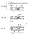
- Fig. 1 schematically shows, in a cross-sectional view, the constitution of an interposer according to one embodiment of the present invention.
- the constitution of the interposer is shown in a simplified manner. The detailed constitution (structure) thereof will be described later in conjunction with the process.
- a silicon (Si) chip 1 is mounted as indicated by dashed lines in the drawing.
- the interposer 10 with the Si chip 1 mounted thereon is mounted on a packaging board to constitute a semiconductor device.
- the interposer 10 has, as its basic structure, a portion 11 (hereinafter referred to as a "Si interposer portion") which is made of Si necessary for matching its coefficient of thermal expansion (CTE) with that of the Si chip 1 to be mounted thereon, and a portion 12 (hereinafter referred to as an "extended interposer portion") which is extended to the periphery (around the Si interposer portion 11 in the plane thereof) of a chip mount area in order to realize a required fan-out structure.
- Si interposer portion a portion 11
- CTE coefficient of thermal expansion
- the Si interposer portion 11 and the extended interposer portion 12 are integrally provided.
- the Si interposer portion 11 has a size approximately equal to that of the Si chip 1 to be mounted thereon, when viewed two-dimensionally.
- the extended interposer portion 12 is made of an insulator. In this embodiment, epoxy resin is used in consideration of cost (reduction in cost) and processing (ease of processing).
- wiring patterns 14a and 14b are formed in required shapes with insulating layers 13a and 13b interposed therebetween, respectively.
- the wiring patterns 14a and 14b are electrically connected to each other via through holes formed at required positions in the Si interposer portion 11.
- wiring patterns 15a and 15b are formed in required shapes, respectively.
- the wiring patterns 15a and 15b are electrically connected to each other via through holes formed at required positions in the extended interposer portion 12.
- the through holes formed in the interposer portions 11 and 12 are filled with conductors (e.g., Cu). Alternatively, conductors are formed on the inner walls thereof.
- the wiring patterns 14a and 14b of the Si interposer portion 11 and the wiring patterns 15a and 15b of the extended interposer portion 12 are connected to each other at required positions.
- Each of the wiring patterns 14a, 14b, 15a, and 15b is formed to include pad portions at required positions.
- the wiring patterns 14a and 15a on the side where the Si chip 1 is to be mounted are formed in such a manner that pad portions are delimited at positions corresponding to the positions of electrode terminals 2 (e.g., solder bumps or gold (Au) stud bumps) of the Si chip 1 to be mounted, and the wiring patterns 14b and 15b on the opposite side are formed in such a manner that pad portions are delimited at positions corresponding to the bonding positions of external connection terminals 16 (e.g., solder bumps) which are to be used when the interposer 10 is mounted on a packaging board.
- electrode terminals 2 e.g., solder bumps or gold (Au) stud bumps
- the structure is shown in which one layer of wiring patterns 14a and 14b (15a and 15b) is formed on each surface of the interposer portion 11 (12).
- the number of wiring layers may be further increased by a build-up process or the like, as needed.
- protective films e.g., solder resist layers
- protective films are formed on both surfaces of the interposer portions 11 and 12 so as to cover the entire surface in such a manner that the pad portions of the wiring patterns 14a, 14b, 15a, and 15b are exposed.
- plated layers of nickel (Ni)/gold (Au) are deposited on the wiring patterns (pad portions) exposed from the protective films.
- the external connection terminals 16 are provided, but these terminals do not necessarily need to be provided. It suffices that the pad portions (plated Ni/Au layers) are exposed from the protective films so that external connection terminals can be bonded thereto when necessary.
- the interposer 10 basically has the following features: there are integrally provided the Si interposer portion 11 having the size necessary for matching its CTE with that of the Si chip 1 to be mounted thereon, and the extended interposer portion 12 necessary to realize a required fan-out structure; and multilayer stacking can be realized using the pad portions exposed from the protective films or the external connection terminals bonded to the pad portions, as needed as described later.
- the interposer portion 11 made of Si is provided as a component for performing CTE matching with the Si chip 1.
- the material of the interposer portion 11 is not limited to Si as long as it is a material having a CTE equivalent to that of the Si chip 1.
- low firing temperature ceramic such as glass ceramic can be suitably used.
- Fig. 2 schematically shows one example of the constitution of a semiconductor device constituted using the interposer 10 according to the above-described embodiment.
- the illustrated semiconductor device 50 is constituted by mounting the interposer 10 with the Si chip 1 mounted thereon on a printed wiring board (packaging board) 51 such as a mother board.
- a printed wiring board (packaging board) 51 such as a mother board.
- the flip-chip bonding of the chip is performed in such a manner that the electrode terminals 2, such as solder bumps, which are bonded to the pads of the Si chip 1 are electrically connected to the pad portions of the wiring pattern which are exposed from the solder resist layer (protective film) on the upper side, and furthermore, underfill resin (e.g., epoxy resin) is filled into the space between the chip and the solder resist layer, and cured, whereby the Si chip 1 is bonded to the interposer 10.
- underfill resin e.g., epoxy resin
- solder balls to serve as external connection terminals are bonded by reflow to the pad portions of the wiring patterns which are exposed from the solder resist layer (protective film) on the lower side, and the pad portions are connected via the solder bumps 16 to corresponding pads or lands 52 on the printed wiring board 51.
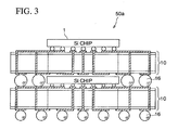
- Fig. 3 schematically shows another example of the constitution of a semiconductor device constituted using the interposer 10 according to the above-described embodiment.
- the illustrated semiconductor device 50a has a structure in which a plurality of interposers 10 (two interposers in the illustrated example) with Si chips 1 mounted thereon are electrically connected to each other and stacked in a multilayered manner.
- the electrical connection between the interposers 10 is established via the pad portions (on the upper side) of the lower interposer 10 and the external connection terminals 16 bonded to the pad portions (on the lower side) of the upper interposer 10.
- the printed wiring board (packaging board) 51 shown in Fig. 2 is not shown in the example shown in Fig. 3.
- a semiconductor device can also be constituted in the constitution in which a plurality of interposers 10 according to this embodiment are two-dimensionally arranged.
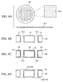
- FIG. 4A to 6C showing one example of a fabricating process thereof.
- Figs. 4A to 6C for simplification of illustration, only (part of) the Si interposer portion 11 and (part of) the extended interposer portion 12 adjacent thereto are shown.
- RIE reactive ion etching
- an insulating layer 21 of SiO 2 (silicon oxide film) is formed on the entire surface including the inner walls of the through holes TH1, for example, by CVD or thermal oxidation.
- a seed layer 22 of copper (Cu) is formed on the entire surface of the insulating layer 21, for example, by electroless plating, sputtering, or vapor deposition.
- the through holes TH1 are filled with conductors, and wiring patterns 23 are formed in required shapes on both surfaces to be connected to the conductors.
- the through holes TH1 are filled by electrolytic Cu plating.
- conductive paste containing metal such as Cu is filled into the through holes TH1 by screen printing, inkjet printing, or the like.
- the Cu wiring patterns 23 having required shapes are formed on the filled conductors by a subtractive process, a semi-additive process, inkjet printing, or the like. Where a semi-additive process or inkjet printing is used, the wiring patterns 23 can be formed simultaneously with the filling of the through holes TH1 with conductors (Cu). This contributes to a simplification of the process.
- the wiring patterns 23 formed here correspond to the wiring patterns 14a and 14b shown in Fig. 1.
- the number of layers of wiring patterns to be formed is not limited to two. The number of layers of wiring may be appropriately increased by a build-up process or the like, as needed.
- the Si wafer 20 with the wiring patterns 23 formed on both surfaces thereof is cut into individual shapes (in this embodiment, the shapes of Si chips 1 to be mounted) of Si interposer portions 11 as seen two-dimensionally, for example, using a dicer, to be divided into individual pieces, each corresponding to one interposer.
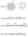
- a supporting body 24 is prepared in which an insulating film 25 made of epoxy resin, polyimide resin, or the like, is formed on one surface thereof.
- the Si interposer portions 11 (each of which is part of the interposer 10) which have been obtained as individual pieces in the preceding step are arranged at a predetermined regular interval therebetween.
- the supporting body 24 may be made of a metal body, or may be in the form of a tape member or the like. In the latter case, it is desirable that the surface of the tape member on which the insulating film 25 is to be formed is coated with a release agent. That is because such an agent makes it convenient when the supporting body 24 is stripped off and removed in a later stage.
- resin is filled into the gaps between the Si interposer portions 11 to form a resin layer 26.
- an insulating film 27 is formed on the Si interposer portions 11 and the resin layer 26 by CVD, lamination, or the like.
- the resin layer 26 can be formed as follows: a low-viscosity thermosetting epoxy resin is melted and poured into the gaps between the Si interposer portions 11, and directly subjected to hot pressing from above.
- Part of the resin layer 26 formed here constitute the extended interposer portions 12 shown in Fig. 1. Further, the insulating films 27 and 25 formed on both surfaces of the Si interposer portions 11 and the resin layer 26 with the Si interposer portions 11 and the resin layer 26 interposed therebetween correspond to the insulating layers 13a and 13b shown in Fig. 1, respectively.
- the supporting body 24 (Fig. 5C) is removed by wet etching (in the case of a metal), stripping-off (in the case of a tape member), or the like.
- through holes TH2 are formed at required positions in the resin layer 26 (including the insulating films 25 and 27), for example, using a mechanical drill, a UV-YAG laser, a CO 2 laser, or an excimer laser. Further, via holes VH are formed on required portions (pad portions) of the wiring patterns 23 of the Si interposer portions 11 so as to reach the pad portions, for example, using a laser.
- a seed layer (Cu) is formed on the entire surfaces of the insulating films 25 and 27 including the insides of the through holes TH2 and the via holes VH by electroless plating, sputtering, or the like.
- the through holes TH2 and the via holes VH are filled by electrolytic Cu plating (alternatively, conductive paste containing metal such as Cu is filled into the through holes TH2 by screen printing, inkjet printing, or the like).
- Cu wiring patterns 28 having required shapes are formed by a subtractive process, a semi-additive process, inkjet printing, or the like, so as to connect the conductors filled in the through holes TH2 and the pad portions of the wiring patterns 23 which are exposed from the via holes VH.
- the wiring patterns 28 formed here correspond to the wiring patterns 15a and 15b shown in Fig. 1.
- solder resist layers 29 are formed to cover the entire surface in such a manner that the pad portions delimited at required positions in the wiring patterns 28 on both surfaces are exposed. Further, the pad portions (Cu) exposed from the solder resist layers 29 are plated with Ni/Au (formation of plated Ni/Au layers 30). This is intended to obtain improved adhesiveness with the pad portions when solder bonding is performed in a later stage. Furthermore, portions of the resin layer 26 (including the insulating films 25 and 27) are cut in such a manner that specified areas for the extended interposer portions 12 (Fig. 1) are delimited, thereby separating pieces, each including one Si interposer portion 11.
- the interposer 10 is fabricated.
- solder bumps to be used as the external connection terminals 16 may be formed on the pad portions (one plated Ni/Au layer 30) which are exposed from one solder resist layer 29, as needed.
- the Si interposer portion 11 has a size approximately equal to that of the Si chip 1 to be mounted thereon. Accordingly, it is possible to match its coefficient of thermal expansion (CTE) matching with that of the Si chip 1.
- the extended interposer portion 12 provided in an area (i.e., an area which is essentially unnecessary from the viewpoint of CTE matching with the Si chip 1 to be mounted) around the Si interposer portion 11 is made of an insulator (epoxy resin). Accordingly, Si does not need to be used for an unnecessary area as heretofore, and the amount of Si used can be reduced to a required minimum. Thus, cost can be reduced. Further, the presence of the extended interposer portion 12 makes it possible to realize a required fan-out structure.
- processing is performed after the Si interposer portions 11 have been cut and separated from the Si wafer 20 and re-laid out on the supporting body 24. Accordingly, unlike the case where processing is performed on the whole Si wafer without cut and separation of the Si interposer portions as heretofore, required wiring patterns can be easily formed on both surfaces of the interposer 10.
- the stress can be removed by dicing to be performed in a later stage (Fig. 5A). Accordingly, the processing becomes easy due to the thin Si wafer. This can contribute to a reduction in the thickness of the interposer 10.
- a wiring board process can be used for processing the through holes and for forming electrical paths in the through holes. Accordingly, the process can be simplified. This makes it possible to reduce cost and to shorten a procedure.
- the material constituting the extended interposer portion 12 is not limited to this.
- the extended interposer portion 12 can also be made of a metal body instead of an insulator.
- the extended interposer portion is made of a metal body.
- the constitution of an interposer according to this embodiment is the same as that of the interposer 10 shown in Fig. 1 in terms of the appearance, and therefore will not be further described here.
- the constitution of the interposer (for the case where the extended interposer portion is made of a metal body) according to this embodiment also provides the advantage in that heat generated inside can be dissipated into the outside environment when the interposer is constituted as a semiconductor device, because the extended interposer portion is made of a metal body.
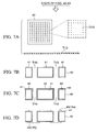
- Figs. 4A to 5A are performed.
- Fig. 7A through holes TH3 are formed at required positions in a metal plate 40 of aluminum (A1), copper (Cu), or the like, having a predetermined thickness (approximately 50 to 300 ⁇ m) by wet etching; a hole-making process using a mechanical drill; laser processing using a UV-YAG laser, a CO 2 laser, an excimer laser, or the like. In doing so, an opening portion for accommodating the Si interposer portion 11 may be simultaneously formed.
- a seed layer 42 of copper (Cu) is formed on the entire surface of the insulating layer 41, for example, by electroless plating, sputtering, or vapor deposition.
- the through holes TH3 are filled with conductors, and wiring patterns 43 having required shapes are formed on both surfaces so as to be connected to these conductors.
- the through holes TH3 are filled by electrolytic Cu plating.
- conductive paste containing metal such as Cu is filled into the through holes TH3 by screen printing, inkjet printing, or the like.
- Cu wiring patterns 43 having required shapes are formed on the filled conductors by a subtractive process, a semi-additive process, inkjet printing, or the like. Where a semi-additive process or inkjet printing is used, the wiring patterns 43 can be formed simultaneously with the filling of the through holes TH3 with conductors (Cu) (simplification of process).
- the wiring patterns 43 formed here correspond to the wiring patterns 15a and 15b shown in Fig. 1.
- the number of layers of wiring patterns to be formed is not limited to two. The number of layers of wiring may be appropriately increased by a build-up process or the like, as needed.
- the metal plate 40 with the wiring patterns 43 formed on both surfaces thereof is cut into the shapes of required extended interposer portions 12a (part of the interposer), i.e., "frame-like" shapes in which an opening portion OP for accommodating the Si interposer portion 11 is formed as shown in the drawing, to be divided into individual pieces, each corresponding to one interposer.
- the opening portion for accommodating the Si interposer portion 11 is formed by cutting using a dicer or the like in this step.
- the opening portion may be formed by stamping using a press or the like.
- a supporting body 44 is prepared with an insulating film 45 made of epoxy resin, polyimide resin, or the like, formed on one surface thereof.
- the Si interposer portions 11 already obtained as individual pieces and the extended interposer portions 12a obtained as individual pieces in the preceding step are arranged.
- the Si interposer portion 11 is arranged in such a manner that it is accommodated in the opening portion OP formed in the extended interposer portion 12a.
- the supporting body 44 may be made of a metal body, or may be in the form of a tape member or the like (here, the surface thereof on which the insulating film 45 is formed is coated with a release agent).
- an insulating film 46 is formed on the entire surface including the spaces between the Si interposer portions 11 and the extended interposer portions 12a and the spaces between adjacent extended interposer portions 12a, by CVD, lamination, or the like.
- thermosetting resin may be applied to the entire surface and cured to form the insulating film 46.
- the insulating film 46 formed here and the insulating film 45 formed in the preceding step correspond to the insulating layers 13a and 13b shown in Fig. 1, respectively.
- the supporting body 44 (Fig. 8C) is removed by wet etching (in the case of a metal), stripping-off (in the case of a tape member), or the like.
- via holes VH1 and VH2 are formed on required portions (pad portions) of the wiring patterns 23 and 43 of the Si interposer portions 11 and the extended interposer portions 12a so as to reach the pad portions, for example, using a UV-YAG laser, a CO 2 laser, or an excimer laser.
- Cu wiring patterns 47 having required shapes are formed by a subtractive process, a semi-additive process, screen printing using conductive paste, or the like, so as to connect the pad portions of the wiring patterns 23 which are exposed from the via holes VH1 formed in the Si interposer portions 11 and the pad portions of the wiring patterns 43 which are exposed from the via holes VH2 formed in the extended interposer portions 12a.
- the wiring patterns 47 formed here correspond to the wiring patterns 15a and 15b shown in Fig. 1.
- solder resist layers 29 are formed to cover the entire surface in such a manner that the pad portions delimited at required positions in the wiring patterns 47 on both surfaces are exposed. Further, the pad portions (Cu) exposed from the solder resist layers 29 are plated with Ni/Au (formation of plated Ni/Au layers 30). Furthermore, insulating film portions around the extended interposer portions 12a are cut, thereby separating pieces, in such a manner that one Si interposer portion 11 and the extended interposer portion 12a placed around the Si interposer portion 11 are included in each piece.
- the interposer 10a is fabricated.
- solder bumps (external connection terminals 16 in Fig. 1) may be formed on the pad portions (one plated Ni/Au layer 30) which are exposed from one solder resist layer 29, as needed.
- Figs. 4A to 5A are performed.
- Fig. 10A through holes TH4 are formed at required positions in a metal plate 40 of aluminum (A1), copper (Cu), or the like, having a predetermined thickness (approximately 50 to 300 ⁇ m) by wet etching; a hole-making process using a mechanical drill; laser processing using a CO 2 laser, an excimer laser, or the like.
- the metal plate 40 is cut into the shapes of required extended interposer portions 12b, i.e., "frame-like" shapes in which an opening portion OP for accommodating the Si interposer portion 11 is formed as shown in the drawing, to be divided into individual pieces, each corresponding to one interposer.
- a supporting body 44 is prepared in which an insulating film 45 made of epoxy resin, polyimide resin, or the like, is formed on one surface thereof.
- the Si interposer portions 11 already obtained as individual pieces and the extended interposer portions 12b obtained as individual pieces in the preceding step are arranged. In doing so, the Si interposer portion 11 is arranged in such a manner that it is accommodated in the opening portion formed in the extended interposer portion 12b.
- the supporting body 44 may be made of a metal body, or may be in the form of a tape member or the like (here, the surface thereof on which the insulating film 45 is formed is coated with a release agent).
- an insulating film 46 is formed on the entire surface including the spaces between the Si interposer portions 11 and the extended interposer portions 12b and the spaces between adjacent extended interposer portions 12b, by CVD, lamination, or the like. At this time, the insulating film is also formed (filled) in the through holes TH4 formed in the metal plate 40.
- the insulating film 46 may be formed by applying and curing thermosetting resin.
- the insulating film 46 formed here and the insulating film 45 formed in the preceding step correspond to the insulating layers 13a and 13b shown in Fig. 1, respectively.
- the supporting body 44 (Fig. 10C) is removed by wet etching (in the case of a metal), stripping-off (in the case of a tape member), or the like.
- through holes TH5 are formed at predetermined positions (positions of the through holes TH4 filled with an insulating film) in the extended interposer portions 12b, for example, using a UV-YAG laser, a CO 2 laser, or an excimer laser. Furthermore, via holes VH3 are formed on required portions (pad portions) of the wiring patterns 23 of the Si interposer portions 11 so as to reach the pad portions, for example, using a laser.
- a seed layer (Cu) is formed on the entire surface including the insides of the through holes TH5 by electroless plating, sputtering, or the like.
- the through holes TH5 are filled by electrolytic Cu plating.
- conductive paste (conductors 48) containing metal such as Cu is filled into the through holes TH5 by screen printing, inkjet printing, or the like.
- Cu wiring patterns 47 having required shapes are formed by a subtractive process, a semi-additive process, inkjet printing, or the like, so as to connect the conductors 48 filled in the through holes TH5 and the pad portions of the wiring patterns 23 which are exposed from the via holes VH3.
- the wiring patterns 47 formed here correspond to the wiring patterns 15a and 15b shown in Fig. 1.
- solder resist layers 29 are formed to cover the entire surface in such a manner that the pad portions delimited at required positions in the wiring patterns 47 on both surfaces are exposed. Further, the pad portions (Cu) exposed from the solder resist layers 29 are plated with Ni/Au (formation of plated Ni/Au layers 30). Furthermore, insulating film portions around the extended interposer portions 12b are cut to be separated into pieces, in such a manner that one Si interposer portion 11 and the extended interposer portion 12b placed around the Si interposer portion 11 are included in each piece.
- solder bumps may be formed on the pad portions (one plated Ni/Au layer 30) which are exposed from one solder resist layer 29, as needed.
Applications Claiming Priority (1)
| Application Number | Priority Date | Filing Date | Title |
|---|---|---|---|
| JP2004193490A JP4343044B2 (ja) | 2004-06-30 | 2004-06-30 | インターポーザ及びその製造方法並びに半導体装置 |
Publications (3)
| Publication Number | Publication Date |
|---|---|
| EP1612860A2 true EP1612860A2 (fr) | 2006-01-04 |
| EP1612860A3 EP1612860A3 (fr) | 2007-05-30 |
| EP1612860B1 EP1612860B1 (fr) | 2017-06-14 |
Family
ID=35058144
Family Applications (1)
| Application Number | Title | Priority Date | Filing Date |
|---|---|---|---|
| EP05253670.3A Active EP1612860B1 (fr) | 2004-06-30 | 2005-06-14 | Dispositif semi-conducteur comprenant un interposeur et un procédé de fabrication pour un dispositif semi-conducteur comprenant un interposeur |
Country Status (4)
| Country | Link |
|---|---|
| US (2) | US7388293B2 (fr) |
| EP (1) | EP1612860B1 (fr) |
| JP (1) | JP4343044B2 (fr) |
| CN (1) | CN1716587B (fr) |
Cited By (4)
| Publication number | Priority date | Publication date | Assignee | Title |
|---|---|---|---|---|
| CN101295691B (zh) * | 2007-04-27 | 2010-12-08 | 台湾积体电路制造股份有限公司 | 半导体封装结构 |
| EP2006911A3 (fr) * | 2007-06-22 | 2011-08-03 | Shinko Electric Industries Co., Ltd. | Substrat de câblage |
| EP2595188A1 (fr) * | 2011-11-17 | 2013-05-22 | ST-Ericsson SA | Paquet de circuit |
| US11348890B2 (en) | 2016-05-06 | 2022-05-31 | Smoltek Ab | Assembly platform |
Families Citing this family (125)
| Publication number | Priority date | Publication date | Assignee | Title |
|---|---|---|---|---|
| US20050046016A1 (en) * | 2003-09-03 | 2005-03-03 | Ken Gilleo | Electronic package with insert conductor array |
| US6987314B1 (en) * | 2004-06-08 | 2006-01-17 | Amkor Technology, Inc. | Stackable semiconductor package with solder on pads on which second semiconductor package is stacked |
| JP4063796B2 (ja) * | 2004-06-30 | 2008-03-19 | 日本電気株式会社 | 積層型半導体装置 |
| US7659623B2 (en) * | 2005-04-11 | 2010-02-09 | Elpida Memory, Inc. | Semiconductor device having improved wiring |
| US20060270104A1 (en) * | 2005-05-03 | 2006-11-30 | Octavio Trovarelli | Method for attaching dice to a package and arrangement of dice in a package |
| JP4507101B2 (ja) * | 2005-06-30 | 2010-07-21 | エルピーダメモリ株式会社 | 半導体記憶装置及びその製造方法 |
| JP4716819B2 (ja) * | 2005-08-22 | 2011-07-06 | 新光電気工業株式会社 | インターポーザの製造方法 |
| US7829989B2 (en) * | 2005-09-07 | 2010-11-09 | Alpha & Omega Semiconductor, Ltd. | Vertical packaged IC device modules with interconnected 3D laminates directly contacts wafer backside |
| JP4473807B2 (ja) * | 2005-10-27 | 2010-06-02 | パナソニック株式会社 | 積層半導体装置及び積層半導体装置の下層モジュール |
| JP5259053B2 (ja) | 2005-12-15 | 2013-08-07 | パナソニック株式会社 | 半導体装置および半導体装置の検査方法 |
| US7684205B2 (en) * | 2006-02-22 | 2010-03-23 | General Dynamics Advanced Information Systems, Inc. | System and method of using a compliant lead interposer |
| US7390700B2 (en) * | 2006-04-07 | 2008-06-24 | Texas Instruments Incorporated | Packaged system of semiconductor chips having a semiconductor interposer |
| US7633168B2 (en) * | 2006-06-28 | 2009-12-15 | Intel Corporation | Method, system, and apparatus for a secure bus on a printed circuit board |
| DE602006021413D1 (de) * | 2006-07-14 | 2011-06-01 | Stmicroelectronics Ltd Malta | Gehäuse für MEMS Bauteile |
| US20080017407A1 (en) * | 2006-07-24 | 2008-01-24 | Ibiden Co., Ltd. | Interposer and electronic device using the same |
| US7518229B2 (en) * | 2006-08-03 | 2009-04-14 | International Business Machines Corporation | Versatile Si-based packaging with integrated passive components for mmWave applications |
| JP2008091638A (ja) | 2006-10-02 | 2008-04-17 | Nec Electronics Corp | 電子装置およびその製造方法 |
| US7616451B2 (en) | 2006-10-13 | 2009-11-10 | Stmicroelectronics S.R.L. | Semiconductor package substrate and method, in particular for MEMS devices |
| US7791199B2 (en) * | 2006-11-22 | 2010-09-07 | Tessera, Inc. | Packaged semiconductor chips |
| US8569876B2 (en) | 2006-11-22 | 2013-10-29 | Tessera, Inc. | Packaged semiconductor chips with array |
| JP4870584B2 (ja) * | 2007-01-19 | 2012-02-08 | ルネサスエレクトロニクス株式会社 | 半導体装置 |
| TW200833202A (en) * | 2007-01-26 | 2008-08-01 | Advanced Semiconductor Eng | Method for manufacturing a circuit board |
| JP4970979B2 (ja) * | 2007-02-20 | 2012-07-11 | ルネサスエレクトロニクス株式会社 | 半導体装置 |
| JP5584474B2 (ja) | 2007-03-05 | 2014-09-03 | インヴェンサス・コーポレイション | 貫通ビアによって前面接点に接続された後面接点を有するチップ |
| TWI335654B (en) * | 2007-05-04 | 2011-01-01 | Advanced Semiconductor Eng | Package for reducing stress |
| US20080284037A1 (en) * | 2007-05-15 | 2008-11-20 | Andry Paul S | Apparatus and Methods for Constructing Semiconductor Chip Packages with Silicon Space Transformer Carriers |
| US9601412B2 (en) * | 2007-06-08 | 2017-03-21 | Cyntec Co., Ltd. | Three-dimensional package structure |
| US7982137B2 (en) * | 2007-06-27 | 2011-07-19 | Hamilton Sundstrand Corporation | Circuit board with an attached die and intermediate interposer |
| CN103178032B (zh) | 2007-07-31 | 2017-06-20 | 英闻萨斯有限公司 | 使用穿透硅通道的半导体封装方法 |
| JPWO2009084301A1 (ja) | 2007-12-28 | 2011-05-12 | イビデン株式会社 | インターポーザー及びインターポーザーの製造方法 |
| WO2009084300A1 (fr) | 2007-12-28 | 2009-07-09 | Ibiden Co., Ltd. | Interposeur et procédé de fabrication de l'interposeur |
| JP5224845B2 (ja) | 2008-02-18 | 2013-07-03 | 新光電気工業株式会社 | 半導体装置の製造方法及び半導体装置 |
| JPWO2009113198A1 (ja) | 2008-03-14 | 2011-07-21 | イビデン株式会社 | インターポーザー及びインターポーザーの製造方法 |
| SG177945A1 (en) * | 2008-07-18 | 2012-02-28 | United Test & Assembly Ct Lt | Packaging structural member |
| US10026720B2 (en) | 2015-05-20 | 2018-07-17 | Broadpak Corporation | Semiconductor structure and a method of making thereof |
| US9818680B2 (en) * | 2011-07-27 | 2017-11-14 | Broadpak Corporation | Scalable semiconductor interposer integration |
| US8014166B2 (en) * | 2008-09-06 | 2011-09-06 | Broadpak Corporation | Stacking integrated circuits containing serializer and deserializer blocks using through silicon via |
| US9893004B2 (en) * | 2011-07-27 | 2018-02-13 | Broadpak Corporation | Semiconductor interposer integration |
| US9164404B2 (en) | 2008-09-19 | 2015-10-20 | Intel Corporation | System and process for fabricating semiconductor packages |
| US9165841B2 (en) * | 2008-09-19 | 2015-10-20 | Intel Corporation | System and process for fabricating semiconductor packages |
| JP5596919B2 (ja) * | 2008-11-26 | 2014-09-24 | キヤノン株式会社 | 半導体装置の製造方法 |
| JP5456411B2 (ja) * | 2009-08-19 | 2014-03-26 | ルネサスエレクトロニクス株式会社 | 半導体装置及び半導体装置の製造方法 |
| KR101139147B1 (ko) * | 2009-09-11 | 2012-04-26 | 파나소닉 주식회사 | 전자 부품 실장체 및 그 제조 방법 및 인터포저 |
| JP5330184B2 (ja) * | 2009-10-06 | 2013-10-30 | 新光電気工業株式会社 | 電子部品装置 |
| US8866258B2 (en) * | 2009-10-06 | 2014-10-21 | Broadcom Corporation | Interposer structure with passive component and method for fabricating same |
| US8592973B2 (en) * | 2009-10-16 | 2013-11-26 | Stats Chippac Ltd. | Integrated circuit packaging system with package-on-package stacking and method of manufacture thereof |
| TWI392069B (zh) * | 2009-11-24 | 2013-04-01 | Advanced Semiconductor Eng | 封裝結構及其封裝製程 |
| US8164917B2 (en) * | 2009-12-23 | 2012-04-24 | Oracle America, Inc. | Base plate for use in a multi-chip module |
| EP2339627A1 (fr) * | 2009-12-24 | 2011-06-29 | Imec | Emballage de moule interposé de fenêtre |
| US8884422B2 (en) * | 2009-12-31 | 2014-11-11 | Stmicroelectronics Pte Ltd. | Flip-chip fan-out wafer level package for package-on-package applications, and method of manufacture |
| KR20110088234A (ko) * | 2010-01-28 | 2011-08-03 | 삼성전자주식회사 | 적층 반도체 패키지의 제조 방법 |
| US10297550B2 (en) | 2010-02-05 | 2019-05-21 | Taiwan Semiconductor Manufacturing Company, Ltd. | 3D IC architecture with interposer and interconnect structure for bonding dies |
| US20110193235A1 (en) * | 2010-02-05 | 2011-08-11 | Taiwan Semiconductor Manufacturing Company, Ltd. | 3DIC Architecture with Die Inside Interposer |
| JP5560793B2 (ja) * | 2010-03-16 | 2014-07-30 | 凸版印刷株式会社 | シリコン配線基板 |
| TWI442534B (zh) * | 2010-04-12 | 2014-06-21 | Hon Hai Prec Ind Co Ltd | 晶片轉接板 |
| US8455995B2 (en) | 2010-04-16 | 2013-06-04 | Taiwan Semiconductor Manufacturing Company, Ltd. | TSVs with different sizes in interposers for bonding dies |
| US8913402B1 (en) * | 2010-05-20 | 2014-12-16 | American Semiconductor, Inc. | Triple-damascene interposer |
| US9640437B2 (en) | 2010-07-23 | 2017-05-02 | Tessera, Inc. | Methods of forming semiconductor elements using micro-abrasive particle stream |
| US8791575B2 (en) | 2010-07-23 | 2014-07-29 | Tessera, Inc. | Microelectronic elements having metallic pads overlying vias |
| US8796135B2 (en) | 2010-07-23 | 2014-08-05 | Tessera, Inc. | Microelectronic elements with rear contacts connected with via first or via middle structures |
| TWI446420B (zh) | 2010-08-27 | 2014-07-21 | Advanced Semiconductor Eng | 用於半導體製程之載體分離方法 |
| TWI445152B (zh) | 2010-08-30 | 2014-07-11 | Advanced Semiconductor Eng | 半導體結構及其製作方法 |
| US9007273B2 (en) | 2010-09-09 | 2015-04-14 | Advances Semiconductor Engineering, Inc. | Semiconductor package integrated with conformal shield and antenna |
| US8610259B2 (en) | 2010-09-17 | 2013-12-17 | Tessera, Inc. | Multi-function and shielded 3D interconnects |
| US8847380B2 (en) | 2010-09-17 | 2014-09-30 | Tessera, Inc. | Staged via formation from both sides of chip |
| TWI434387B (zh) | 2010-10-11 | 2014-04-11 | Advanced Semiconductor Eng | 具有穿導孔之半導體裝置及具有穿導孔之半導體裝置之封裝結構及其製造方法 |
| US9064879B2 (en) | 2010-10-14 | 2015-06-23 | Taiwan Semiconductor Manufacturing Company, Ltd. | Packaging methods and structures using a die attach film |
| US8936966B2 (en) | 2012-02-08 | 2015-01-20 | Taiwan Semiconductor Manufacturing Company, Ltd. | Packaging methods for semiconductor devices |
| US8105875B1 (en) | 2010-10-14 | 2012-01-31 | Taiwan Semiconductor Manufacturing Company, Ltd. | Approach for bonding dies onto interposers |
| KR101191247B1 (ko) | 2010-10-28 | 2012-10-16 | (주) 트라이스시스템 | Fbga패키지 및 그 제조 방법 |
| US8970240B2 (en) * | 2010-11-04 | 2015-03-03 | Cascade Microtech, Inc. | Resilient electrical interposers, systems that include the interposers, and methods for using and forming the same |
| TWI527174B (zh) | 2010-11-19 | 2016-03-21 | 日月光半導體製造股份有限公司 | 具有半導體元件之封裝結構 |
| US8637968B2 (en) * | 2010-12-02 | 2014-01-28 | Tessera, Inc. | Stacked microelectronic assembly having interposer connecting active chips |
| US8736066B2 (en) | 2010-12-02 | 2014-05-27 | Tessera, Inc. | Stacked microelectronic assemby with TSVS formed in stages and carrier above chip |
| US8587126B2 (en) | 2010-12-02 | 2013-11-19 | Tessera, Inc. | Stacked microelectronic assembly with TSVs formed in stages with plural active chips |
| US8610264B2 (en) | 2010-12-08 | 2013-12-17 | Tessera, Inc. | Compliant interconnects in wafers |
| TWI445155B (zh) | 2011-01-06 | 2014-07-11 | Advanced Semiconductor Eng | 堆疊式封裝結構及其製造方法 |
| US8853819B2 (en) | 2011-01-07 | 2014-10-07 | Advanced Semiconductor Engineering, Inc. | Semiconductor structure with passive element network and manufacturing method thereof |
| US20120187545A1 (en) * | 2011-01-24 | 2012-07-26 | Broadcom Corporation | Direct through via wafer level fanout package |
| KR101817159B1 (ko) | 2011-02-17 | 2018-02-22 | 삼성전자 주식회사 | Tsv를 가지는 인터포저를 포함하는 반도체 패키지 및 그 제조 방법 |
| KR20130007049A (ko) * | 2011-06-28 | 2013-01-18 | 삼성전자주식회사 | 쓰루 실리콘 비아를 이용한 패키지 온 패키지 |
| US8780576B2 (en) * | 2011-09-14 | 2014-07-15 | Invensas Corporation | Low CTE interposer |
| US9013037B2 (en) | 2011-09-14 | 2015-04-21 | Stmicroelectronics Pte Ltd. | Semiconductor package with improved pillar bump process and structure |
| DE102011083223B4 (de) * | 2011-09-22 | 2019-08-22 | Infineon Technologies Ag | Leistungshalbleitermodul mit integrierter Dickschichtleiterplatte |
| US9679863B2 (en) * | 2011-09-23 | 2017-06-13 | STATS ChipPAC Pte. Ltd. | Semiconductor device and method of forming interconnect substrate for FO-WLCSP |
| US10475759B2 (en) * | 2011-10-11 | 2019-11-12 | Taiwan Semiconductor Manufacturing Company, Ltd. | Integrated circuit structure having dies with connectors of different sizes |
| US8916481B2 (en) | 2011-11-02 | 2014-12-23 | Stmicroelectronics Pte Ltd. | Embedded wafer level package for 3D and package-on-package applications, and method of manufacture |
| US8541883B2 (en) | 2011-11-29 | 2013-09-24 | Advanced Semiconductor Engineering, Inc. | Semiconductor device having shielded conductive vias |
| CN104471708B (zh) * | 2012-02-08 | 2017-05-24 | 吉林克斯公司 | 具有多个插入件的堆叠裸片组件 |
| US8975157B2 (en) | 2012-02-08 | 2015-03-10 | Advanced Semiconductor Engineering, Inc. | Carrier bonding and detaching processes for a semiconductor wafer |
| US8963316B2 (en) | 2012-02-15 | 2015-02-24 | Advanced Semiconductor Engineering, Inc. | Semiconductor device and method for manufacturing the same |
| US8786060B2 (en) | 2012-05-04 | 2014-07-22 | Advanced Semiconductor Engineering, Inc. | Semiconductor package integrated with conformal shield and antenna |
| US9153542B2 (en) | 2012-08-01 | 2015-10-06 | Advanced Semiconductor Engineering, Inc. | Semiconductor package having an antenna and manufacturing method thereof |
| US8937387B2 (en) | 2012-11-07 | 2015-01-20 | Advanced Semiconductor Engineering, Inc. | Semiconductor device with conductive vias |
| US8952542B2 (en) | 2012-11-14 | 2015-02-10 | Advanced Semiconductor Engineering, Inc. | Method for dicing a semiconductor wafer having through silicon vias and resultant structures |
| US9406552B2 (en) | 2012-12-20 | 2016-08-02 | Advanced Semiconductor Engineering, Inc. | Semiconductor device having conductive via and manufacturing process |
| US8841751B2 (en) | 2013-01-23 | 2014-09-23 | Advanced Semiconductor Engineering, Inc. | Through silicon vias for semiconductor devices and manufacturing method thereof |
| US9059241B2 (en) | 2013-01-29 | 2015-06-16 | International Business Machines Corporation | 3D assembly for interposer bow |
| US9978688B2 (en) | 2013-02-28 | 2018-05-22 | Advanced Semiconductor Engineering, Inc. | Semiconductor package having a waveguide antenna and manufacturing method thereof |
| US9226396B2 (en) * | 2013-03-12 | 2015-12-29 | Invensas Corporation | Porous alumina templates for electronic packages |
| US9089268B2 (en) | 2013-03-13 | 2015-07-28 | Advanced Semiconductor Engineering, Inc. | Neural sensing device and method for making the same |
| US9173583B2 (en) | 2013-03-15 | 2015-11-03 | Advanced Semiconductor Engineering, Inc. | Neural sensing device and method for making the same |
| US8987734B2 (en) | 2013-03-15 | 2015-03-24 | Advanced Semiconductor Engineering, Inc. | Semiconductor wafer, semiconductor process and semiconductor package |
| TWI503934B (zh) * | 2013-05-09 | 2015-10-11 | Advanced Semiconductor Eng | 半導體元件及其製造方法及半導體封裝結構 |
| US20150004750A1 (en) * | 2013-06-27 | 2015-01-01 | Stats Chippac, Ltd. | Methods of Forming Conductive Materials on Contact Pads |
| US9735082B2 (en) | 2013-12-04 | 2017-08-15 | Taiwan Semiconductor Manufacturing Company, Ltd. | 3DIC packaging with hot spot thermal management features |
| US9646917B2 (en) * | 2014-05-29 | 2017-05-09 | Invensas Corporation | Low CTE component with wire bond interconnects |
| JP2016029681A (ja) * | 2014-07-25 | 2016-03-03 | イビデン株式会社 | 多層配線板及びその製造方法 |
| US10177115B2 (en) | 2014-09-05 | 2019-01-08 | Taiwan Semiconductor Manufacturing Company, Ltd. | Package structures and methods of forming |
| JP6473595B2 (ja) | 2014-10-10 | 2019-02-20 | イビデン株式会社 | 多層配線板及びその製造方法 |
| EP3053191A4 (fr) * | 2014-12-16 | 2017-06-28 | Intel Corporation | Assemblage électronique comprenant des dispositifs électroniques empilés |
| US9837345B2 (en) * | 2015-07-17 | 2017-12-05 | Ibiden Co., Ltd. | Interposer and circuit substrate |
| US9648729B1 (en) * | 2015-11-20 | 2017-05-09 | Raytheon Company | Stress reduction interposer for ceramic no-lead surface mount electronic device |
| US9721923B1 (en) * | 2016-04-14 | 2017-08-01 | Micron Technology, Inc. | Semiconductor package with multiple coplanar interposers |
| CN207781947U (zh) * | 2017-03-10 | 2018-08-28 | 唐虞企业股份有限公司 | 连接器 |
| US11646288B2 (en) * | 2017-09-29 | 2023-05-09 | Intel Corporation | Integrating and accessing passive components in wafer-level packages |
| JP2018050077A (ja) * | 2017-12-14 | 2018-03-29 | ルネサスエレクトロニクス株式会社 | 電子装置 |
| WO2019146039A1 (fr) * | 2018-01-25 | 2019-08-01 | ソフトバンク株式会社 | Système de refroidissement à base de liquide de refroidissement pour circuit intégré empilé tridimensionnel, et circuit intégré empilé tridimensionnel l'utilisant |
| WO2019181589A1 (fr) * | 2018-03-23 | 2019-09-26 | 株式会社村田製作所 | Module haute fréquence et dispositif de communication |
| CN213366570U (zh) * | 2018-03-23 | 2021-06-04 | 株式会社村田制作所 | 高频模块和通信装置 |
| US10916492B2 (en) * | 2018-05-11 | 2021-02-09 | Advanced Semiconductor Engineering, Inc. | Semiconductor substrate and method of manufacturing the same |
| JP7215322B2 (ja) * | 2019-05-17 | 2023-01-31 | 株式会社デンソー | 電子装置 |
| JP2021106341A (ja) * | 2019-12-26 | 2021-07-26 | 株式会社村田製作所 | 高周波モジュールおよび通信装置 |
| CN113363161A (zh) * | 2021-05-21 | 2021-09-07 | 广东佛智芯微电子技术研究有限公司 | 内置高散热通路的板级扇出型封装结构及其制备方法 |
| US20230102345A1 (en) * | 2021-09-24 | 2023-03-30 | Texas Instruments Incorporated | Planar surfaces on substrates |
Citations (1)
| Publication number | Priority date | Publication date | Assignee | Title |
|---|---|---|---|---|
| JP2001326305A (ja) | 2000-05-12 | 2001-11-22 | Shinko Electric Ind Co Ltd | 半導体装置用インターポーザー、その製造方法および半導体装置 |
Family Cites Families (18)
| Publication number | Priority date | Publication date | Assignee | Title |
|---|---|---|---|---|
| CA2002213C (fr) * | 1988-11-10 | 1999-03-30 | Iwona Turlik | Boitier de puce de circuits integres a haute performance et sa methode de fabrication |
| JP3147087B2 (ja) * | 1998-06-17 | 2001-03-19 | 日本電気株式会社 | 積層型半導体装置放熱構造 |
| US6617681B1 (en) * | 1999-06-28 | 2003-09-09 | Intel Corporation | Interposer and method of making same |
| KR100413789B1 (ko) * | 1999-11-01 | 2003-12-31 | 삼성전자주식회사 | 고진공 패키징 마이크로자이로스코프 및 그 제조방법 |
| US6529027B1 (en) * | 2000-03-23 | 2003-03-04 | Micron Technology, Inc. | Interposer and methods for fabricating same |
| JP3980807B2 (ja) * | 2000-03-27 | 2007-09-26 | 株式会社東芝 | 半導体装置及び半導体モジュール |
| US20020020898A1 (en) * | 2000-08-16 | 2002-02-21 | Vu Quat T. | Microelectronic substrates with integrated devices |
| EP1354351B1 (fr) * | 2000-08-16 | 2009-04-15 | Intel Corporation | Couche formee directement sur un boitier a puce encapsule |
| US6525407B1 (en) * | 2001-06-29 | 2003-02-25 | Novellus Systems, Inc. | Integrated circuit package |
| US6717066B2 (en) * | 2001-11-30 | 2004-04-06 | Intel Corporation | Electronic packages having multiple-zone interconnects and methods of manufacture |
| FR2834385A1 (fr) * | 2001-12-28 | 2003-07-04 | St Microelectronics Sa | Commutateur statique bidirectionnel sensible dans les quadrants q4 et q1 |
| US6911733B2 (en) * | 2002-02-28 | 2005-06-28 | Hitachi, Ltd. | Semiconductor device and electronic device |
| JP2004079701A (ja) * | 2002-08-14 | 2004-03-11 | Sony Corp | 半導体装置及びその製造方法 |
| JP2004128063A (ja) * | 2002-09-30 | 2004-04-22 | Toshiba Corp | 半導体装置及びその製造方法 |
| AU2003244322A1 (en) * | 2002-11-21 | 2004-06-15 | Hitachi, Ltd. | Electronic device |
| WO2004047167A1 (fr) * | 2002-11-21 | 2004-06-03 | Nec Corporation | Dispositif a semiconducteur, substrat de cablage, et procede pour produire un substrat de cablage |
| JP2004273563A (ja) * | 2003-03-05 | 2004-09-30 | Shinko Electric Ind Co Ltd | 基板の製造方法及び基板 |
| JP4621049B2 (ja) * | 2005-03-25 | 2011-01-26 | 富士通株式会社 | 配線基板の製造方法 |
-
2004
- 2004-06-30 JP JP2004193490A patent/JP4343044B2/ja not_active Expired - Fee Related
-
2005
- 2005-06-14 EP EP05253670.3A patent/EP1612860B1/fr active Active
- 2005-06-14 US US11/151,193 patent/US7388293B2/en active Active
- 2005-06-16 CN CN2005100774268A patent/CN1716587B/zh active Active
-
2006
- 2006-07-19 US US11/488,648 patent/US7415762B2/en active Active
Patent Citations (1)
| Publication number | Priority date | Publication date | Assignee | Title |
|---|---|---|---|---|
| JP2001326305A (ja) | 2000-05-12 | 2001-11-22 | Shinko Electric Ind Co Ltd | 半導体装置用インターポーザー、その製造方法および半導体装置 |
Cited By (4)
| Publication number | Priority date | Publication date | Assignee | Title |
|---|---|---|---|---|
| CN101295691B (zh) * | 2007-04-27 | 2010-12-08 | 台湾积体电路制造股份有限公司 | 半导体封装结构 |
| EP2006911A3 (fr) * | 2007-06-22 | 2011-08-03 | Shinko Electric Industries Co., Ltd. | Substrat de câblage |
| EP2595188A1 (fr) * | 2011-11-17 | 2013-05-22 | ST-Ericsson SA | Paquet de circuit |
| US11348890B2 (en) | 2016-05-06 | 2022-05-31 | Smoltek Ab | Assembly platform |
Also Published As
| Publication number | Publication date |
|---|---|
| JP4343044B2 (ja) | 2009-10-14 |
| JP2006019368A (ja) | 2006-01-19 |
| EP1612860A3 (fr) | 2007-05-30 |
| EP1612860B1 (fr) | 2017-06-14 |
| CN1716587B (zh) | 2011-12-07 |
| CN1716587A (zh) | 2006-01-04 |
| US20060001179A1 (en) | 2006-01-05 |
| US7388293B2 (en) | 2008-06-17 |
| US20060263937A1 (en) | 2006-11-23 |
| US7415762B2 (en) | 2008-08-26 |
Similar Documents
| Publication | Publication Date | Title |
|---|---|---|
| US7415762B2 (en) | Interposer, method of fabricating the same, and semiconductor device using the same | |
| US7122901B2 (en) | Semiconductor device | |
| US11309304B2 (en) | Stackable electronic package and method of fabricating same | |
| JP4899604B2 (ja) | 三次元半導体パッケージ製造方法 | |
| US6271056B1 (en) | Stacked semiconductor package and method of fabrication | |
| EP1356519B1 (fr) | Boitier microelectronique a substrat integre | |
| US7944039B2 (en) | Semiconductor device and method of manufacturing the same | |
| JP6342120B2 (ja) | 超薄埋設ダイモジュール及びその製造方法 | |
| US8872041B2 (en) | Multilayer laminate package and method of manufacturing the same | |
| US7768119B2 (en) | Carrier structure embedded with semiconductor chip | |
| KR100851072B1 (ko) | 전자 패키지 및 그 제조방법 | |
| US9679837B2 (en) | Electrical interconnect for an integrated circuit package and method of making same | |
| JP5367523B2 (ja) | 配線基板及び配線基板の製造方法 | |
| JP2013243345A5 (fr) | ||
| JP2004537841A (ja) | ウェハレベルで形成される集積回路パッケージ | |
| JP2005005632A (ja) | チップ状電子部品及びその製造方法、並びにその実装構造 | |
| US6432748B1 (en) | Substrate structure for semiconductor package and manufacturing method thereof | |
| US7785928B2 (en) | Integrated circuit device and method of manufacturing thereof | |
| JP4528018B2 (ja) | 半導体装置及びその製造方法 | |
| JP2005011856A (ja) | チップ状電子部品及びその製造方法、並びにその実装構造 | |
| JP6034664B2 (ja) | 半導体装置、半導体積層モジュール構造、積層モジュール構造、及びこれらの製造方法 |
Legal Events
| Date | Code | Title | Description |
|---|---|---|---|
| PUAI | Public reference made under article 153(3) epc to a published international application that has entered the european phase |
Free format text: ORIGINAL CODE: 0009012 |
|
| AK | Designated contracting states |
Kind code of ref document: A2 Designated state(s): AT BE BG CH CY CZ DE DK EE ES FI FR GB GR HU IE IS IT LI LT LU MC NL PL PT RO SE SI SK TR |
|
| AX | Request for extension of the european patent |
Extension state: AL BA HR LV MK YU |
|
| PUAL | Search report despatched |
Free format text: ORIGINAL CODE: 0009013 |
|
| AK | Designated contracting states |
Kind code of ref document: A3 Designated state(s): AT BE BG CH CY CZ DE DK EE ES FI FR GB GR HU IE IS IT LI LT LU MC NL PL PT RO SE SI SK TR |
|
| AX | Request for extension of the european patent |
Extension state: AL BA HR LV MK YU |
|
| 17P | Request for examination filed |
Effective date: 20071126 |
|
| AKX | Designation fees paid |
Designated state(s): DE |
|
| 17Q | First examination report despatched |
Effective date: 20080411 |
|
| GRAP | Despatch of communication of intention to grant a patent |
Free format text: ORIGINAL CODE: EPIDOSNIGR1 |
|
| INTG | Intention to grant announced |
Effective date: 20170109 |
|
| RIN1 | Information on inventor provided before grant (corrected) |
Inventor name: FUKASE, KATSUYA C/O SHINKO ELECTRIC INDUSTRIES CO. Inventor name: WAKABAYASHI, SHINICHI C/O SHINKO ELECTRIC INDUSTRI |
|
| GRAS | Grant fee paid |
Free format text: ORIGINAL CODE: EPIDOSNIGR3 |
|
| GRAA | (expected) grant |
Free format text: ORIGINAL CODE: 0009210 |
|
| AK | Designated contracting states |
Kind code of ref document: B1 Designated state(s): DE |
|
| REG | Reference to a national code |
Ref country code: DE Ref legal event code: R096 Ref document number: 602005052115 Country of ref document: DE |
|
| REG | Reference to a national code |
Ref country code: DE Ref legal event code: R097 Ref document number: 602005052115 Country of ref document: DE |
|
| PLBE | No opposition filed within time limit |
Free format text: ORIGINAL CODE: 0009261 |
|
| STAA | Information on the status of an ep patent application or granted ep patent |
Free format text: STATUS: NO OPPOSITION FILED WITHIN TIME LIMIT |
|
| 26N | No opposition filed |
Effective date: 20180315 |
|
| REG | Reference to a national code |
Ref country code: DE Ref legal event code: R082 Ref document number: 602005052115 Country of ref document: DE Representative=s name: HL KEMPNER PATENTANWAELTE, SOLICITORS (ENGLAND, DE Ref country code: DE Ref legal event code: R082 Ref document number: 602005052115 Country of ref document: DE Representative=s name: HL KEMPNER PATENTANWALT, RECHTSANWALT, SOLICIT, DE |
|
| PGFP | Annual fee paid to national office [announced via postgrant information from national office to epo] |
Ref country code: DE Payment date: 20230502 Year of fee payment: 19 |