EP1562240A2 - Elektroden für einen OTFT - Google Patents
Elektroden für einen OTFT Download PDFInfo
- Publication number
- EP1562240A2 EP1562240A2 EP05002139A EP05002139A EP1562240A2 EP 1562240 A2 EP1562240 A2 EP 1562240A2 EP 05002139 A EP05002139 A EP 05002139A EP 05002139 A EP05002139 A EP 05002139A EP 1562240 A2 EP1562240 A2 EP 1562240A2
- Authority
- EP
- European Patent Office
- Prior art keywords
- electrode
- organic semiconductor
- transistor
- substrate
- thin film
- Prior art date
- Legal status (The legal status is an assumption and is not a legal conclusion. Google has not performed a legal analysis and makes no representation as to the accuracy of the status listed.)
- Withdrawn
Links
Images



Classifications
-
- H—ELECTRICITY
- H10—SEMICONDUCTOR DEVICES; ELECTRIC SOLID-STATE DEVICES NOT OTHERWISE PROVIDED FOR
- H10K—ORGANIC ELECTRIC SOLID-STATE DEVICES
- H10K71/00—Manufacture or treatment specially adapted for the organic devices covered by this subclass
- H10K71/60—Forming conductive regions or layers, e.g. electrodes
- H10K71/611—Forming conductive regions or layers, e.g. electrodes using printing deposition, e.g. ink jet printing
-
- H—ELECTRICITY
- H10—SEMICONDUCTOR DEVICES; ELECTRIC SOLID-STATE DEVICES NOT OTHERWISE PROVIDED FOR
- H10K—ORGANIC ELECTRIC SOLID-STATE DEVICES
- H10K10/00—Organic devices specially adapted for rectifying, amplifying, oscillating or switching; Organic capacitors or resistors having potential barriers
- H10K10/40—Organic transistors
- H10K10/46—Field-effect transistors, e.g. organic thin-film transistors [OTFT]
- H10K10/462—Insulated gate field-effect transistors [IGFETs]
- H10K10/464—Lateral top-gate IGFETs comprising only a single gate
-
- H—ELECTRICITY
- H10—SEMICONDUCTOR DEVICES; ELECTRIC SOLID-STATE DEVICES NOT OTHERWISE PROVIDED FOR
- H10K—ORGANIC ELECTRIC SOLID-STATE DEVICES
- H10K10/00—Organic devices specially adapted for rectifying, amplifying, oscillating or switching; Organic capacitors or resistors having potential barriers
- H10K10/40—Organic transistors
- H10K10/46—Field-effect transistors, e.g. organic thin-film transistors [OTFT]
- H10K10/462—Insulated gate field-effect transistors [IGFETs]
- H10K10/468—Insulated gate field-effect transistors [IGFETs] characterised by the gate dielectrics
- H10K10/471—Insulated gate field-effect transistors [IGFETs] characterised by the gate dielectrics the gate dielectric comprising only organic materials
-
- H—ELECTRICITY
- H10—SEMICONDUCTOR DEVICES; ELECTRIC SOLID-STATE DEVICES NOT OTHERWISE PROVIDED FOR
- H10K—ORGANIC ELECTRIC SOLID-STATE DEVICES
- H10K10/00—Organic devices specially adapted for rectifying, amplifying, oscillating or switching; Organic capacitors or resistors having potential barriers
- H10K10/40—Organic transistors
- H10K10/46—Field-effect transistors, e.g. organic thin-film transistors [OTFT]
- H10K10/462—Insulated gate field-effect transistors [IGFETs]
- H10K10/481—Insulated gate field-effect transistors [IGFETs] characterised by the gate conductors
-
- H—ELECTRICITY
- H10—SEMICONDUCTOR DEVICES; ELECTRIC SOLID-STATE DEVICES NOT OTHERWISE PROVIDED FOR
- H10K—ORGANIC ELECTRIC SOLID-STATE DEVICES
- H10K10/00—Organic devices specially adapted for rectifying, amplifying, oscillating or switching; Organic capacitors or resistors having potential barriers
- H10K10/80—Constructional details
- H10K10/82—Electrodes
- H10K10/86—Schottky electrodes
-
- H—ELECTRICITY
- H10—SEMICONDUCTOR DEVICES; ELECTRIC SOLID-STATE DEVICES NOT OTHERWISE PROVIDED FOR
- H10K—ORGANIC ELECTRIC SOLID-STATE DEVICES
- H10K77/00—Constructional details of devices covered by this subclass and not covered by groups H10K10/80, H10K30/80, H10K50/80 or H10K59/80
- H10K77/10—Substrates, e.g. flexible substrates
- H10K77/111—Flexible substrates
-
- H—ELECTRICITY
- H10—SEMICONDUCTOR DEVICES; ELECTRIC SOLID-STATE DEVICES NOT OTHERWISE PROVIDED FOR
- H10K—ORGANIC ELECTRIC SOLID-STATE DEVICES
- H10K85/00—Organic materials used in the body or electrodes of devices covered by this subclass
- H10K85/10—Organic polymers or oligomers
- H10K85/111—Organic polymers or oligomers comprising aromatic, heteroaromatic, or aryl chains, e.g. polyaniline, polyphenylene or polyphenylene vinylene
-
- H—ELECTRICITY
- H10—SEMICONDUCTOR DEVICES; ELECTRIC SOLID-STATE DEVICES NOT OTHERWISE PROVIDED FOR
- H10K—ORGANIC ELECTRIC SOLID-STATE DEVICES
- H10K85/00—Organic materials used in the body or electrodes of devices covered by this subclass
- H10K85/10—Organic polymers or oligomers
- H10K85/151—Copolymers
-
- H—ELECTRICITY
- H10—SEMICONDUCTOR DEVICES; ELECTRIC SOLID-STATE DEVICES NOT OTHERWISE PROVIDED FOR
- H10K—ORGANIC ELECTRIC SOLID-STATE DEVICES
- H10K10/00—Organic devices specially adapted for rectifying, amplifying, oscillating or switching; Organic capacitors or resistors having potential barriers
- H10K10/80—Constructional details
- H10K10/82—Electrodes
-
- Y—GENERAL TAGGING OF NEW TECHNOLOGICAL DEVELOPMENTS; GENERAL TAGGING OF CROSS-SECTIONAL TECHNOLOGIES SPANNING OVER SEVERAL SECTIONS OF THE IPC; TECHNICAL SUBJECTS COVERED BY FORMER USPC CROSS-REFERENCE ART COLLECTIONS [XRACs] AND DIGESTS
- Y02—TECHNOLOGIES OR APPLICATIONS FOR MITIGATION OR ADAPTATION AGAINST CLIMATE CHANGE
- Y02E—REDUCTION OF GREENHOUSE GAS [GHG] EMISSIONS, RELATED TO ENERGY GENERATION, TRANSMISSION OR DISTRIBUTION
- Y02E10/00—Energy generation through renewable energy sources
- Y02E10/50—Photovoltaic [PV] energy
- Y02E10/549—Organic PV cells
Definitions
- the present invention relates to a transistor, a circuit board, a display and electronic equipment.
- transistors employing organic materials (organic semiconductor materials) that exhibit semi- conducting electrical conductivity have advantages such as suitability for being thinned and lightened, flexibility, low material costs, and so forth, so as to be expected as a switching element of a flexible display and so forth.
- organic materials organic semiconductor materials
- advantages such as suitability for being thinned and lightened, flexibility, low material costs, and so forth, so as to be expected as a switching element of a flexible display and so forth.
- a source electrode and a drain electrode are formed on a substrate while an organic semiconductor layer, a gate insulating layer and a gate electrode are deposited above these electrodes in that order.
- These transistors can be fabricated in the atmosphere by using vapor deposition or a coating method (for example, refer to Patent Documents 1, 2, 3 and 4).
- the fact that these transistors can be fabricated in the atmosphere does not necessarily lead to the stable operation thereof in the atmosphere.
- the organic semiconductor layer is doped with oxygen and water, which increases an off-state current, or in contrast increases traps so as to cause the deterioration of subthreshold swing (S value) and threshold voltage (Vth).
- S value subthreshold swing
- Vth threshold voltage
- a method of sealing a transistor has been proposed as a method of preventing an organic semiconductor layer from being doped with oxygen and water in.the atmosphere.
- a transistor is fabricated on a glass substrate and then an encapsulating film is deposited in vacuum so as to cover the transistor, thereby sealing it. This prevents the organic semiconductor layer from being doped with oxygen and water, and thus the characteristics of the transistor can be stabilized. Also, a method has been proposed in which a multilayer of inorganic films and polymer films alternately deposited is used as an encapsulating film for further enhancing the encapsulating characteristic.
- the methods of sealing a transistor involve a problem that the transistor becomes expensive because vacuum treatment and heat treatment are required.
- a gas barrier film also needs to be formed on the plastic substrate side because of the low gas-barrier characteristic of plastic materials, causing a problem that costs are further increased.
- a non-flexible component material for example, silicon oxide or silicon nitride
- the transistor thus fabricated exerts a comparatively high encapsulating characteristic, it is impossible to obtain a complete encapsulation. Therefore, if a transistor is subjected to a high temperature and high humidity environment and oxygen and water enter the inside thereof once, the high encapsulating characteristic functions adversely. That is, even when the transistor is brought back to a low temperature and low humidity environment, the oxygen and water are not discharged outside the transistor but remain in the inside thereof for a long time. Such a transistor therefore involves a problem that oxygen and water trapped therein deteriorates the characteristics of the transistor.
- the present invention is intended to provide a transistor that can maintain its high characteristics even after being subjected to a high temperature and high humidity environment, a circuit board, a display and electronic equipment that include the transistor.
- a transistor of the present invention comprises:
- the transistor of the present invention it is preferable that the transistor has a top gate structure and the gate electrode is made up of the porous film. With this structure, the transistor can maintain its high characteristics even after being subj ected to a high temperature and high humid environment.
- porosity of the porous film is preferably from 20% to 85%. This porosity can more surely discharge oxygen and water that have entered the inside, and can adequately prevent the conductivity of the porous film from lowering.
- the porous film preferably has a carbon atom or a carbon compound in a pore of the porous film. This enables the inner surfaces of the pores to be endowed with hydrophobicity, and therefore can prevent dew condensation (accumulation) from being generated when water or the like passes through the pores. Thus the transformation and deterioration of the porous film can adequately be prevented.
- the porous film is preferably formed by using a liquid material including an electrically conductive particle. This facilitates the formation of a porous film having an intended porosity.
- the conductive particle preferably comprises as a main component at least one of gold, silver, copper, platinum, palladium, nickel, and an alloy including these elements. These substances are preferable because of high electrical conductivity.
- the liquid material preferably comprises the conductive particle and a dispersion medium including water.
- the porous film is preferably formed by using a coating method. Thus, the porous film can be formed more easily.
- the coating method is preferably an ink jet method.
- the ink jet method permits the formation of a porous film with high dimensional accuracy.
- the porous film is preferably obtained through a heating process. This heating process can easily and surely remove substances that are included in the liquid material and should be removed.
- heating temperature in the heating process is preferably equal to or smaller than 200 °C. This can surely prevent the lowering of the porosity.
- the conductive material preferably comprises a metal material and/or a metal oxide material as a main component. Thus, the porous film having high conductivity can be formed.
- the organic semiconductor layer is preferably composed mainly of a polymer including arylamine or a derivative of the polymer.
- the organic semiconductor layer composed of such an organic semiconductor material has high water-resistance and oxidation-resistance characteristics. Therefore, the organic semiconductor layer is chemically stable particularly and the quality deterioration thereof is avoided even when it is temporarily subjected to a high temperature and high humidity environment.
- the organic semiconductor layer is preferably composed mainly of a copolymer including fluorene and bithiophene, or a derivative of the copolymer.
- the organic semiconductor layer composed of such an organic semiconductor material has high water-resistance and oxidation-resistance characteristics. Therefore, the organic semiconductor layer is chemically stable particularly and the quality deterioration thereof is avoided even when it is temporarily subjected to a high temperature and high humidity environment.
- the organic semiconductor layer is preferably formed by using an ink jet method.
- the organic semiconductor layer having an intended shape can be formed with high dimensional accuracy.
- both of the source electrode and the drain electrode are preferably formed in a comb teeth shape and in such a manner that the teeth interdigitate with each other. This form can prevent the increase of the area of an overlapping part between the gate electrode and the source and drain electrodes, and thus the characteristics of the transistor can further be enhanced.
- a circuit board of the present invention comprises a plurality of the transistors of the present invention. This can provide a highly reliable circuit board.
- the circuit board of the present invention at least a part of the gate electrode provided for the transistors is made up of a common electrode. This structure facilitates the formation of a gate electrode, reducing the manufacturing time of the circuit board.
- the common electrode is preferably almost linear.
- a display of the present invention comprises:
- the display of the present invention preferably further comprises a protective film provided closer to the circuit board than the display medium so as to cover the transistors and the pixel electrodes.
- this structure can adequately prevent shear stress from being placed on the transistor, the display medium, and so forth.
- the display medium preferably comprises a organophilic liquid that dissolves or swells a material constituting the organic semiconductor layer.
- the protective film preferably has a function to prevent the organophilic liquid from diffusing toward the circuit board. This can avoid the dissolution and swelling of the organic semiconductor layer, and therefore can adequately prevent the deterioration of characteristics of the transistor.
- the protective film is preferably composed mainly of a hydrophilic polymer material having hydrophilicity. According to this, even if the organophilic liquid flows out from the display medium, the organophilic liquid can be prevented from passing through the protective film so as to enter the circuit board.
- the polymer material preferably comprises as a main component a polymer including vinyl alcohol. These substances have particularly high hydrophilicity. Therefore, even if the organophilic liquid flows out from the display medium, the organophilic liquid can be prevented from passing through the protective film so as to enter the circuit board particularly effectively.
- Electronic equipment of the present invention comprises the display of the present invention. Thus, the electronic equipment with high reliability can be obtained.
- FIGs. 1A and 1B are diagrams showing a thin film transistor having a first structure.
- FIG. 1A is a longitudinal sectional view
- FIG. 1B is a plan view.
- the upper side in FIG. 1A corresponds to the upper side of the thin film transistor, while the lower side corresponds to the lower side thereof.
- a thin film transistor 1 shown in FIGs. 1A and 1B is provided on a substrate 2, and comprises a source electrode 3 (source electrode fingers 3a) and a drain electrode 4 (drain electrode fingers 4a), an organic semiconductor layer (organic layer) 5, a gate insulating layer 6, and a gate electrode 7 that are deposited in that order from the substrate 2 side.
- both the source electrode 3 and drain electrode 4 are formed on the substrate 2 in comb teeth and in such a manner that the teeth interdigitate with each other.
- the organic semiconductor layer 5 is provided so as to cover and be in contact with the electrodes 3 and 4.
- the gate insulating layer 6 is provided on and in contact with the organic semiconductor layer 5.
- the gate electrode 7 is provided so as to overlap, with the intermediary of the gate insulating layer 6, a region in which the teeth of the source and drain electrodes 3 and 4 interdigitate with each other.
- the source electrode 3 and the drain electrode 4 have a plurality of electrode fingers 3a and 4a arranged at certain intervals, respectively, so as to have a comb teeth shape as a whole. Furthermore, the source and drain electrodes 3 and 4 are provided in such a manner that the electrode fingers 3a and 4a are alternately arranged.
- Such a thin film transistor 1 has a structure in which the source and drain electrodes 3 and 4 are provided closer to the substrate 2 than the gate electrode 7, with the gate insulating layer 6 being between the electrodes 3 and 4, and the gate electrode 7. That is, the thin film transistor 1 has a top gate structure.
- the substrate 2 supports each layer (each element) making up the thin-film transistor 1.
- the following substrates can be used as the substrate 2, for example: a glass substrate; a plastic substrate (resin substrate) made up of polyimide, polyethylene terephthalate (PET), polyethylene naphthalate (PEN), polymethylmethacrylate (PMMA), polycarbonate (PC), polyethersulphone (PES), aromatic polyester (liquid crystal polymer), or the like; a quartz substrate; a silicon substrate; and a gallium arsenide substrate.
- a plastic substrate is selected as the substrate 2.
- a lower layer may be provided on the substrate 2.
- the lower layer is provided, for example, with a view to preventing the diffusion of ions from the surface of the substrate 2, or to improving the adhesiveness (bonding characteristic) between the source and drain electrodes 3 and 4 and the substrate 2.
- a component material of a lower layer although there is no limitation, silicon dioxide (SiO 2 ), silicon nitride (SiN), polyimide, polyamide, a polymer that is cross-linked so as to be insolubilized, or the like is preferably used.
- the electrode fingers 3a and 4a of the source and drain electrodes 3 and 4 are provided on the substrate 2 along the channel length L direction in such a manner to be arranged alternately at certain intervals.
- regions between the electrode fingers 3a of the source electrode 3 and the electrode fingers 4a of the drain electrode 4 are channel regions in which carriers move.
- the length of movement direction of carriers in regions between the electrode fmgers 3a of the source electrode 3 and the electrode fmgers 4a of the drain electrode 4 that is, the distance between each of the electrode fingers 3a and 4a corresponds to the channel length L.
- the product of the length ⁇ of the direction perpendicular to the channel length L direction and the number of intervals (gaps) N between the electrode fingers 3a and 4a is the channel width W.
- the width A of the electrode fingers 3a and 4a determines the area of overlapping portions between the source and drain electrodes 3 and 4, and the gate electrode 7. Furthermore, in the present embodiment, the source and drain electrodes 3 and 4 are formed with using a resist layer formed by photolithography as a mask, as described later. Therefore, the width A of the electrode fingers 3a and 4a depends on the accuracy of photolithography. However, the narrowing of the electrode fingers is possible since the accuracy of photolithography is extremely high.
- the gate electrode 7 is formed by an ink jet method as described later and therefore has a comparatively large width, the area of overlapping portions between the gate electrode 7 and the source and drain electrodes 3 and 4 can be prevented from increasing. According to this, the capacitance of the gate can be reduced in the thin film transistor 1. As a result, a good characteristic (switching characteristic) is exhibited. As above, since there is no need to form the gate electrode 7 in a minute shape in the present embodiment, the range of options in a forming method thereof is widened. Thus the thin film transistor 1 having a good characteristic is obtained even if various coating methods (particularly ink jet method) are used for forming the gate electrode 7.
- a component material of these source and drain electrodes 3 and 4 is not particularly limited as long as it has electrical conductively.
- one or a combination of two or more of the following substances can be used as the material: conductive materials such as Pd, Pt, Au, W, Ta, Mo, Al, Cr, Ti, Cu, and an alloy including these elements; conductive oxides such as ITO, FTO, ATO and SnO 2 ; carbon materials such as a carbon black, a carbon nanotube and a fullerene; and conductive polymer materials such as a polyacetylene, a polypyrrole, a polythiophene like a poly-ethylenedioxythiophene (PEDOT), a polyaniline, a poly(p-phenylene), a polyfluorene, a polycarbazole, a polysilane, and a derivative of these substances.
- conductive materials such as Pd, Pt, Au, W, Ta, Mo, Al, Cr, Ti, Cu, and an alloy including these
- the conductive polymer material is typically used after being doped with a high molecular weight material of an iron oxide, iodine, an inorganic acid, an organic acid, or a polystyrene sulfonic acid so as to be endowed with electrical conductivity.
- a material made up mainly of Ni, Cu, Co, Au, Pd, or an alloy including these elements is preferably used as a component material of the source and drain electrodes 3 and 4.
- the electrodes 3 and 4 of high deposition accuracy can easily be formed at low costs by using electroless plating in a forming process of the electrodes 3 and 4 to be described later, enabling the fabrication of the thin film transistor 1 having high characteristics.
- the thickness (in average) of the source and drain electrodes 3 and 4 is preferably, but not limited to, about 30-300 nm, and is more preferably about 50-150 nm.
- the width A of the electrode fingers 3a and 4a is preferably 20 ⁇ m or less, and is more preferably 10 ⁇ m or less.
- the distance (separation distance) between the source electrode finger 3a and the drain electrode finger 4a is preferably about 2-20 ⁇ m, and is more preferably about 3-10 ⁇ m.
- the smaller channel length L permits the control of a larger drain current, and enables the capacitance of the gate electrode to be reduced to a smaller value.
- the channel length L is smaller than the above lower limit, a highly accurate photolithography technique is required for patterning the electrodes, causing cost rise.
- the small channel length L is achieved, expected effects are not obtained because of the contact resistance between the source electrode and the organic semiconductor layer in many cases.
- the channel length L is larger than the above upper limit, a drain current becomes small and therefore the characteristics of the thin film transistor 1 may be insufficient.
- the channel width W is preferably about 0.1-5 mm, and is more preferably about 0.3-3 mm. If the channel width W is smaller than the above lower limit, a drain current becomes small and therefore the characteristics of the thin film transistor 1 may be insufficient. In contrast, the channel width W is larger than the above upper limit, the size of the thin film transistor 1 increases while the increase of the parasitic capacitance and the increase of a leak current to the gate electrode 7 through the gate insulating layer 6 may be caused.
- the organic semiconductor layer 5 is provided on and in contact with the substrate 2 so as to cover the source and drain electrodes 3 and 4.
- the organic semiconductor layer 5 is composed mainly of an organic semiconductor material (organic material exhibiting semiconducting electrical conductivity).
- the organic semiconductor layer 5 is preferably oriented so as to be almost parallel with the channel length L direction at least in channel regions 51. This enhances the carrier mobility in the channel regions 51, with the result that the operation speed of the thin film transistor 1 is further enhanced.
- examples of an organic semiconductor material include low molecular weight organic semiconductor materials such as a naphthalene, anthracene, tetracene, pentacene, hexacene, phtalocyanine, perylene, hydrazone, triphenylmethane, diphenylmethane, stilbene, aryl vinyl, pyrazoline, triphenylamine, triarylamine, oligothiophene, and derivative of these substances.
- organic semiconductor materials such as a naphthalene, anthracene, tetracene, pentacene, hexacene, phtalocyanine, perylene, hydrazone, triphenylmethane, diphenylmethane, stilbene, aryl vinyl, pyrazoline, triphenylamine, triarylamine, oligothiophene, and derivative of these substances.
- examples of an organic semiconductor material include polymer organic semiconductor materials (conjugated polymer material) such as a poly(N-vinylcarbazole), polyvinylpyrene, polyvinylanthracene, polythiophene, polyhexylthiophene, poly(p-phenylenevinylene), polythienylenevinylene, polyarylamine, pyrene formaldehyde resin, ethylcarbazole formaldehyde resin, fluorene-bithiophene copolymer, fluorene-arylamine copolymer, and derivative of these substances.
- polymer organic semiconductor materials conjuggated polymer material
- conjuggated polymer material such as a poly(N-vinylcarbazole), polyvinylpyrene, polyvinylanthracene, polythiophene, polyhexylthiophene, poly(p-phenylenevinylene), polythienylenevinylene, polyarylamine, pyr
- a material made up mainly of a polymer organic semiconductor material conjugated polymer material
- the mobility of carriers is particularly high because of the particular distribution of electron clouds therein.
- a polymer organic semiconductor material can be deposited with a simple method and can be oriented comparatively easily.
- an organic semiconductor material is preferably made up mainly of at least one of a copolymer including a fluorene and bithiophene such as a fluorene-bithiophene copolymer, a polymer including an arylamine such as a polyarylamine or fluorine-arylamine copolymer, and a derivative of these substances.
- An organic semiconductor material is more preferably made up mainly of at least one of a polyarylamine, a fluorene-bithiophene copolymer, and a derivative of these substances.
- the organic semiconductor layer 5 composed of such an organic semiconductor material has high water-resistance and oxidation-resistance characteristics. Therefore, the organic semiconductor layer 5 is chemically stable particularly and the quality deterioration thereof is avoided even when it is temporarily subj ected to a high temperature and high humidity environment.
- the organic semiconductor layer 5 including a polymer organic semiconductor material as a main material can be formed in a thinned and lightened manner, and is superior in flexibility. Therefore, it is suitably applied to a thin film transistor used as a switching element of a flexible display and so forth.
- the thickness (in average) of the organic semiconductor layer 5 is preferably about 0.1-1000 nm, and is more preferably about 1- 500 nm. Also, it is further preferably about 10-100 nm.
- the organic semiconductor layer 5 need not necessarily cover the source and drain electrodes 3 and 4. It is sufficient that the organic semiconductor layer 5 is provided at least on the regions (channel regions 51) between the source and drain electrodes 3 and 4.
- the gate insulating layer 6 is provided on and in contact with the organic semiconductor layer 5. The gate insulating layer 6 insulates the gate electrode 7 from the source and drain electrodes 3 and 4.
- the gate insulating layer 6 is preferably made up mainly of an organic material (particularly organic polymer material).
- the gate insulating layer 6 made up mainly of an organic polymer material is easy to form and can achieve higher adhesiveness with the organic semiconductor layer 5.
- organic polymer material include: acrylic resin such as polystyrene, polyimide, polyamideimide, polyvinylphenylene, polycarbonate (PC) and polymethylmethacrylate (PMMA); fluorine resin such as polytetrafluoroethylene (PTFE); phenol resin such as polyvinylphenol and novolac resin; and olefin resin such as polyethylene, polypropylene, polyisobutylene and polybutene.
- acrylic resin such as polystyrene, polyimide, polyamideimide, polyvinylphenylene, polycarbonate (PC) and polymethylmethacrylate (PMMA)
- fluorine resin such as polytetrafluoroethylene (PTFE)
- phenol resin such as polyvinyl
- the thickness (in average) of the gate insulating layer 6 is preferably, but not limited to, about 10-5000 nm, and is more preferably 100-1000 nm. If the thickness of the gate insulating layer 6 is in the above range, the source and drain electrodes 3 and 4 are surely insulated from the gate electrode 7, while the size of the thin film transistor 1 (the thickness thereof particularly) can be prevented from increasing.
- the gate insulating layer 6 is not limited to a single layer but may have a multi-layered structure.
- an inorganic insulating material such as SiO 2 may be used as a component material of the gate insulating layer 6, for example.
- a solution of polysilicate, polysiloxane or polysilazane is applied and then the coating film is heated in the presence of oxygen or water vapor, whereby SiO 2 can be obtained as the gate insulating layer 6 from the solution material.
- a metal alkoxide solution is applied and then is heated in an oxygen atmosphere, whereby an inorganic insulating material can be obtained (this method is known as a sol-gel method).
- the gate electrode 7 is insulated from the source and drain electrodes 3 and 4 by the intermediary of the gate insulating layer 6.
- the gate electrode 7 is made up of a porous film composed mainly of a conductive material. If the gate electrode is made up of a metal film formed by vapor deposition, although such a gate electrode exhibits a comparatively high encapsulating characteristic as described above, it is impossible to achieve a complete encapsulating characteristic. In such a thin film transistor, therefore, if oxygen and water once enters the inside thereof, the oxygen and water are not discharged outside the thin film transistor but remain therein for a long time. Such a thin film transistor therefore involves a problem that oxygen and water accumulated therein deteriorates the characteristics of the transistor.
- At least one of a source electrode, drain electrode and gate electrode (the gate electrode 7 in the present embodiment) is made up of a porous film composed mainly of a conductive material, whereby the gate electrode 7 has high air permeability.
- the porosity of the porous film is preferably, but not limited to, about 20-85%, and is more preferably about 40-85%. Also, it is further preferably about 60-75%. According to this, oxygen and water that have entered the thin film transistor 1 are more surely discharged therefrom. If the porosity is beyond the above upper limit, the electrical conductivity of the porous film may be extremely lowered depending on the kind or the like of the conductive material.
- examples of a conductive material (metal material or metal oxide material) constituting a porous film include: Ag, Pd, Pt, Au, W, Ta, Mo, Al, Cr, Ti, Cu, Ni, an alloy including these elements, indium tin oxide (ITO), indium oxide (IO), indium zinc oxide (IZO), antimony tin oxide (ATO), and tin dioxide (SnO 2 ).
- ITO indium tin oxide
- IO indium oxide
- IZO indium zinc oxide
- ATO antimony tin oxide
- SnO 2 tin dioxide
- a conductive polymer material as has been cited above as a material for the source and drain electrodes 3 and 4 may be used as a conductive material.
- the thickness (in average) of the porous film (gate electrode 7) is preferably, but not limited to, about 0.1-5000 nm, and is more preferably about 1- 5000 nm. Also, it is further preferably about 10-5000 nm.
- graphite, hydrogen carbon, etc. are listed as a carbon compound.
- This carbon compound may arise (be generated) in a forming process of a first wire 91 (gate electrode 7) to be described later, or may be provided in pores after a porous film is formed, for example.
- the amount of a current flowing between the source and drain electrodes 3 and 4 is controlled by changing a voltage applied to the gate electrode 7.
- both of the source and drain electrodes 3 and 4 are formed in comb teeth and the teeth interdigitate with each other.
- the shape of these electrodes 3 and 4 are not limited thereto.
- both of the electrodes 3 and 4 may be formed in a substantially rectangle and may be juxtaposed to each other at a certain interval.
- the description has been made on the thin film transistor 1 having the gate electrode 7 made up of a porous film.
- at least one of a source electrode, drain electrode and gate electrode may be made up of a porous film.
- the thin film transistor of the present invention may also be applied to, besides a top gate structure, a bottom gate structure thin film transistor.
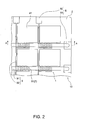
- FIG. 2 is a plan view showing an embodiment of a flexible circuit board of the present invention.
- the near side of FIG. 2 corresponds to the upper side of the circuit board, while the back side corresponds to the lower side thereof.
- a circuit board 10 shown in FIG. 2 comprises the substrate 2, pixel electrodes 41, the thin film transistors 1, connection terminals 8 and wires 9. Each of the elements 41, 1, 8 and 9 is provided on the substrate 2.
- the substrate 2 is a support body for supporting each of the elements 41, 1, 8 and 9 provided thereon.
- the pixel electrodes 41 constitute electrodes of one side that apply a voltage for driving each pixel when an electrophoretic display 20 to be described later is built by using the circuit board 10.
- the pixel electrodes 41 are arranged in a matrix.
- connection terminals 8 comprise a plurality of first terminals 81 and a plurality of second terminals 82.
- Each of the first terminals 81 and each of the second terminals 82 constitute a terminal to be connected to a driving IC.
- the wires 9 are constituted by a plurality of first wires 91 and a plurality of second wires 92 provided almost perpendicularly to the wires 91.
- the gate electrode 7 for the thin film transistors 1 arranged in one row is a common electrode. This common electrode constitutes the first wire 91.
- the first wires 91 are substantially straight.
- One end of each of the first wires 91 is connected to one of the first terminals 81.
- Such a configuration of the first wires 91 enables the gate electrodes 7 of a certain number to be formed at the same time. As a result, the manufacturing time for the circuit board 10 can be shortened. Also, one end of each of the second wires 92 is connected to one of the second terminals 82. The source electrodes 3 of a plurality of the thin film transistors 1 are connected to halfway points of the second wires 92.
- any substance can be used as a component material of the pixel electrodes 41, the connection terminals 8 (first terminals 81 and second terminals 82) and the second wires 92 as long as the substance has electrical conductivity.
- the same substances as have been cited above as a component material of the source and drain electrodes 3 and 4 can be used. According to this, in a manufacturing process of a circuit board to be described later, the source and drain electrodes 3 and 4, the pixel electrodes 41, the connection terminals 8 and the second wires 92 can be formed at the same time in the same process.
- Such a circuit board 10 including a plurality of the thin film transistors 1 is manufactured through the following processes for example.
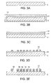
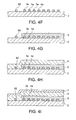
- FIGs. 3A through 3E and 4F through 4I are diagrams (longitudinal sectional views) for explaining a method of forming thin film transistor 1 part (line A-A in FIG. 2) of the circuit board 10.
- the upper side in FIGs. 3A through 3E and 4F through 4I corresponds to the upper side of the thin film transistor, while the lower side corresponds to the lower side thereof.
- a first manufacturing method of the circuit board 10 comprises: (A1) a step of forming source electrodes, drain electrodes, pixel electrodes, wires and connection terminals; (A2) a step of removing organic substances; (A3) a step of forming an organic semiconductor layer; (A4) a step of forming a gate insulating layer; and (A5) a step of forming wires (gate electrodes). Each step will be described below sequentially.
- the source and drain electrodes 3 and 4, the pixel electrodes 41, the connection terminals 8 and the second wires 92 can be formed by forming a film (conductive film) composed of a conductive material, and thereafter removing unwanted portions.
- the film composed of a conductive material is formed by, for example, chemical vapor deposition (CVD) such as plasma CVD, thermal CVD or laser CVD, dry plating such as vapor deposition, sputtering or ion plating, wet plating such as electrolytic plating, immersion plating or electroless plating, spraying, a sol-gel method or metal organic decomposition (MOD).
- the conductive film is preferably formed by electroless plating. The use of electroless plating enables the source and drain electrodes 3 and 4, the pixel electrodes 41, the connection terminals 8 and the second wires 92 to be easily formed with high deposition accuracy at low costs without a large-scale apparatus such as a vacuum apparatus.
- A1-1 First the substrate 2 such as that shown in FIG. 3A is prepared, and then the substrate 2 is cleaned with one or an adequate combination of water (deionized water or the like), an organic solvent, etc. This cleaning improves the wettability of the substrate 2 to water and thus it becomes easy for various treatment liquids described below to contact the substrate 2.
- water deionized water or the like
- organic solvent etc. This cleaning improves the wettability of the substrate 2 to water and thus it becomes easy for various treatment liquids described below to contact the substrate 2.
- step (A1) adhesiveness improving treatment for enhancing the adhesiveness between these elements and the substrate 2 is carried out prior to the present step (A1-1) (step (A1)).
- This adhesiveness improving treatment (surface roughening) is carried out by etching the surface of the substrate 2 with an etchant, and then treating the surface with a treatment liquid including a reducing agent.
- a liquid containing a transition metal oxide such as CrO 3 or MnO 2 and an inorganic acid such as a sulfuric acid or hydrochloric acid can be used as the etchant.
- an agent that does not contain alkali metal elements substantially is used as the reducing agent used as treatment liquid, although there is no limitation. This avoids that alkali metal ions are trapped in the surface of the substrate 2, and thus preventing the diffusion (mixing) of alkali metal ions into the organic semiconductor layer 5 to be formed in the later process. As a result, the deterioration of the characteristics of the organic semiconductor layer 5 can be prevented.
- Ammonium compounds such as ammonium sulfite hydrate and ammonium hypophosphite, hydrazine, etc. are listed as such a reducing agent. Of these substances, an ammonium compound is preferable as a main component of a reducing agent, and ammonium sulfite hydrate is more preferable. An ammonium compound (particularly ammonium sulfite hydrate) is preferable because of excellent reducing properties.
- pre-treatment for forming a plated film 11 is carried out for the substrate 2.
- This pre-treatment is carried out by bringing a solution (surfactant solution) including a cationic surfactant or an anionic surfactant into contact with the substrate 2.
- a solution surfactant solution
- the surface of the substrate 2 is positively charged when a cationic surfactant adheres thereto, while being negatively charged when an anionic surfactant adheres thereto. If the charge polarity of a catalyst used in electroless plating is opposite to the charging of the substrate surface, the catalyst is easily adsorbed.
- the adhesiveness between the plated film 11 (source and drain electrodes 3 and 4, pixel electrodes 41, connection terminals 8 and second wires 92) to be formed and the substrate 2 is enhanced.
- a method of immersing the substrate 2 in a surfactant solution immersion method
- a method of showering (spraying) the substrate 2 with a surfactant solution are listed as a method of contacting a surfactant solution with the substrate 2.
- the immersion method is preferable in particular.
- the immersion method enables a large amount of the substrates 2 to be easily treated.
- a cationic surfactant examples include, for example, alkyl ammonium chloride, benzalkonium chloride, benzethonium chloride and an stearic acid. One or a combination of two or more of these substances can be used.
- the temperature of the surfactant solution for treatment is preferably about 0-70° C, and is more preferably about 10-40° C.
- the treatment time for the substrate 2 in a surfactant solution is preferably about 10-90 seconds, and is more preferably about 30-60 seconds.
- the substrate 2 thus pre-treated is cleaned with using, for example, deionized water (ultrapure water), ion exchange water, distilled water or reverse osmosis (RO) water.
- a catalyst is adsorbed to the surface of the substrate 2.
- a catalyst Au, Ag, Pd, Pt, Ni, etc. are listed. One or a combination of two or more of these elements can be used.
- the substrate 2 is immersed in a colloidal suspension of a Pd alloy such as Sn-Pd or a solution of an ionic Pd catalyst such as palladium chloride, thereby allowing a Pd alloy or ionic Pd catalyst to be adsorbed to the surface of the substrate 2. Thereafter elements irrelevant to catalyzing are removed, whereby Pd is exposed on the surface of the substrate 2.
- the substrate 2 is immersed in the colloidal suspension and then is immersed in an acid solution.
- Sn coordinated to Pd is dissolved so as to be removed, with the result that Pd is exposed on the surface of the substrate 2.
- a solution including an acid such as HBF 4 and a reducing agent such as glucose, or a solution prepared by further adding a sulfuric acid to the solution can be used as the acid solution.
- the temperature of the solution including a catalyst for treatment is preferably about 0-70° C, and is more preferably about 10-40° C.
- the treatment time for the substrate 2 in the solution including a catalyst is preferably from about 10 seconds to about 5 minutes, and is more preferably from about 20 seconds to about 3 minutes.
- the temperature of the acid solution for treatment is preferably about 0-70° C, and is more preferably about 10-40° C.
- the treatment time for the substrate 2 in the acid solution is preferably from about 10 seconds to about 5 minutes, and is more preferably from about 30 seconds to about 3 minutes.
- the substrate 2 to which a catalyst has been thus attached (adsorbed) is cleaned with using, for example, deionized water (ultrapure water), ion exchange water, distilled water or RO water.
- the substrate 2 is immersed in a plating solution 13, thereby allowing metallic elements (elemental metal) to precipitate on the surface of the substrate 2 to form the plated film 11.
- a plating solution 13 used for electroless plating a liquid that includes a metal salt of a metal for forming the plated film 11 (the source and drain electrodes 3 and 4, the pixel electrodes 41, the connection terminals 8 and the second wires 92) and a reducing agent, but not substantially include any alkali metal ions is preferably used.
- a metal salt for example, sulfate salt, nitrate salt, or the like is preferably used.
- a reducing agent for example, hydrazine and ammonium hypophosphite can be cited. Of these substances, at least one of hydrazine and ammonium hypophosphite is preferably used as a main component of a reducing agent.
- the deposition rate of the plated film 11 is made proper.
- the thickness of the film can easily be controlled so as to be within the optimum range of film thickness required for the source and drain electrodes 3 and 4, the pixel electrodes 41, the connection terminals 8 and the second wires 92.
- the resulting plated film 11 can also have an even thickness and preferable surface property (good film surface morphology).
- the amount of a metal salt included in the plating solution 13 (the amount of a metal salt added to a solvent) is preferably about 1-50 g/L, and is more preferably about 5-25 g/L. If the content of a metal salt is too small, it may take a long time to form the plated film 11. In contrast, even if the content of a metal salt is increased beyond the above upper limit, more effectiveness is not expected.
- the amount of a reducing agent included in the plating solution 13 is preferably about 10-200 g/L, and is more preferably about 50-150 g/L.
- a pH adjuster (pH buffer) is further mixed (added) to such a plating solution 13. According to this, it is prevented or suppressed that the pH of the plating solution 13 is lowered as electroless plating proceeds. As a result, the decrease of the deposition rate or changes in the composition or characteristics of the plated film 11 can effectively be prevented.
- a pH adjuster although various kinds can be cited, an adjuster composed mainly of at least one of ammonia water, trimethyl ammonium hydride, and ammonium sulfide is preferable. Since these substances excel in buffering effect, the use of these materials as a pH adjustor provides the above effectiveness more remarkably.
- the pH of the plating solution 13 for the treatment is preferably about 5-12, and is more preferably about 6-10.
- the temperature of the plating solution 13 for the treatment is preferably about 30-90° C, and is more preferably about 40-80° C.
- the treatment time for the substrate 2 in the plating solution 13 is preferably from about 10 seconds to about 5 minutes, and is more preferably from about 20 seconds to about 3 minutes. If the pH and temperature of the plating solution 13 and the treatment time with the plating solution 13 are within the above ranges, the deposition rate becomes particularly proper, and accordingly the plated film 11 having an even thickness can be formed with high precision.
- the thickness of the plated film 11 to be formed can be controlled by arranging the plating conditions such as operation temperature (temperature of a plating solution), operation time (plating time), the amount of a plating solution, the pH of a plating solution, or the number of plating processes (the number of turns). Furthermore, an additive such as a complexing agent or stabilizing agent may be added to the plating solution 13 adequately if necessary.
- carboxylic acids such as an ethylenediamine tetra acetic acid and acetic acid
- oxycarboxylic acids such as a tartaric acid and citric acid
- an aminocarboxylic acid such as glycine
- an amine such as triethanolamine
- polyhidric alcohols such as glycerin and sorbitol
- a stabilizing agent for example, 2, 2'-bipyridyl, cyanide, ferrocyanide, phenanthroline, thiourea, mercaptbenzothiazole, and thioglycolic acid can be cited.
- the substrate 2 on which the plated film 11 has been thus formed is cleaned by using, for example, deionized water (ultrapure water), ion-exchange water, distilled water or RO water.
- a resist layer 12 having a shape corresponding to the shapes of the source and drain electrodes 3 and 4, the pixel electrodes 41, the connection terminals 8 and the second wires 92.
- a resist material 12' is applied (provided) on the plated film 11. Then, the resist material 12' is exposed via a photo mask corresponding to the shapes of the source and drain electrodes 3 and 4, the pixel electrodes 41, the connection terminals 8 and the second wires 92, and then being developed with a developer.
- etching As shown in FIG. 3E, unnecessary portions of the plated film 11 are removed by etching as shown in FIG. 3E.
- This etching can be carried out by using one or a combination of two or more of plasma etching, reactive etching, beam etching, photo-assist etching, other physical etching methods, wet etching, other chemical etching methods, etc.
- the wet etching is preferably used, of these etching methods.
- the etching process can be carried out with simple apparatuses and steps without using any large-scale apparatus such as a vacuum apparatus.
- an etchant used for wet etching for example, a solution including ferric chloride, and a solution including a sulfuric acid, nitric acid, or acetic acid can be cited.
- a resist remover is preferably used for removing the resist layer 12, and besides, for example, the above physical etching methods can also be used.
- the source and drain electrodes 3 and 4 As described above, by using photolithography and etching in combination, the source and drain electrodes 3 and 4, the pixel electrodes 41, the connection terminals 8 and the second wires 92 with high dimensional accuracy can easily and surely be formed. Therefore, the width A of the source electrode fingers 3a and the drain electrode fingers 4a, and the distance (channel length L) between the source electrode finger 3a and the drain electrode finger 4a can be set comparatively shorter, which permits the fabrication of the thin film transistor 1 with a low absolute value of the threshold voltage and large drain current, that is, with excellent characteristics necessary for switching elements.
- either of a negative resist material and a positive resist material can be used as a resist material used in photolithography.
- the description has been made on a method in which the resist layer 12 is formed on the plated film 11 that has been provided on a substrate, and then unnecessary portions of the plated film 11 are removed by etching, as a method of forming the source and drain electrodes 3 and 4, the pixel electrodes 41, the connection terminals 8 and the second wires 92.
- the following method may be used to form each element 3, 4, 41, 8 and 92.
- the resist layer 12 having openings that correspond to the shapes of the elements 3, 4, 41, 8 and 92 is formed on the substrate 2, and then the substrate 2 having the resist layer 12 thereon is immersed in the plating solution 13. Thus a plated film corresponding to the shapes of the elements 3, 4, 41, 8 and 92 is formed. Thereafter the resist layer 12 is removed, thereby obtaining the elements 3, 4, 41, 8 and 92.
- the substrate 2 having the source and drain electrodes 3 and 4, the pixel electrodes 41, the connection terminals 8, and the second wires 92 formed thereon is cleaned with one or an adequate combination of water (deionized water or the like), an organic solvent, etc.
- organic substances existing on the surface of the substrate 2 on which the organic semiconductor layer 5 is to be formed are removed. This removes the barrier to carriers in the interface between the organic semiconductor layer 5 to be formed in the later process and the source and drain electrodes 3 and 4, enabling the improvement of the characteristics of the thin film transistor 1.
- removing method for example, plasma treatment, treatment with ozone water, etching with an acid or alkali, mechanical removal of a surface layer, and ultraviolet rays (UV) (in particular, deep UV) radiation can be cited.
- plasma treatment is preferable as a method of removing organic substances. Plasma treatment enables organic substances to be removed surely in a short time.
- Plasma treatment may be implemented by carrying the substrate 2 in a chamber equipped with a decompression means and a plasma generation means, and then generating plasma in the chamber in a decompressed condition. Alternately, it may be implemented by using a head that has plasma spray nozzles and splaying the substrate surface with plasma. In the latter method, plasma treatment can be carried out in the atmospheric pressure (atmospheric pressure plasma treatment). Therefore, the use of a chamber and decompression means is unnecessary, and thus providing advantages since manufacturing costs and time can be reduced.
- the conditions thereof are as follows for example: the gas flow rate is about 10-300 sccm, and the RF power is about 0.005-0.2 W/cm 2 .
- a gas used for generating plasma is preferably, but not limited to, a gas composed mainly of at least one of oxygen, nitrogen, argon, helium, and fluorocarbon. The mixing of argon or helium into the main component enables plasma to be generated in a comparatively low vacuum atmosphere or under the atmospheric pressure, and thus the apparatus can be simplified. Note that the present step (A2) can be omitted according to need.
- the organic semiconductor layer 5 is formed on the substrate 2 on which the source and drain electrodes 3 and 4, the pixel electrodes 41, the connection terminals 8 and the second wires 92 have been formed, so as to cover the source and drain electrodes 3 and 4.
- the channel regions 51 are formed on regions between the source electrode fingers 3a and the drain electrode fingers 4a.
- the organic semiconductor layer 5 can be formed by applying (supplying) a solution including an organic polymer material or a precursor thereof on the substrate 2 by using a coating method so as to cover the source and drain electrodes 3 and 4, and then carrying out a post-process (e.g., heating, irradiation with infrared rays, or provision of ultrasonic waves) for the coating film according to need.
- a post-process e.g., heating, irradiation with infrared rays, or provision of ultrasonic waves
- Examples of a coating method include, for example, a spin-coating method, a casting method, a micro gravure coating method, a gravure coating method, a bar coating method, a roller coating method, a wire bar coating method, a dip coating method, a spray coating method, a screen printing method, a flexographic printing method, an offset printing method, an ink jet method, and a micro-contact printing method.
- a spin-coating method a casting method
- a micro gravure coating method a gravure coating method
- a bar coating method a roller coating method
- wire bar coating method a roller coating method
- a dip coating method a spray coating method
- a screen printing method a flexographic printing method
- an offset printing method an ink jet method
- micro-contact printing method a micro-contact printing method
- an ink jet method is preferably used for forming the organic semiconductor layer 5.
- An ink jet method allows the organic semiconductor layer 5 to be selectively formed so as to cover only the source and drain electrodes 3 and 4, without supplying a resist layer or the like on the pixel electrodes 41, the connection terminals 8 and the second wires 92. This reduces the amount of a consumed organic semiconductor material, and thereby reducing manufacturing costs.
- the region on which the organic semiconductor layer 5 is formed is not limited to that shown in the drawings.
- the organic semiconductor layer 5 may be formed only in the regions (channel region 51) between the source electrode fingers 3a and the drain electrode fingers 4a. According to this structure, in the case of arranging a plurality of thin film transistors 1 (elements) on a single substrate, leak currents and cross-talk between elements can be suppressed by forming the organic semiconductor layer 5 for each element independently of each other.
- the use of an ink jet method is also particularly suitable for forming the organic semiconductor layer 5 only in the channel regions 51. Furthermore, the required resolution is 5-100 ⁇ m, and therefore matches the resolution by an ink jet method.
- an ink jet method in forming the organic semiconductor layer 5 for each element independently of each other eliminates the need to use chemicals such as photoresist, a developer or a remover, or plasma treatment such as oxygen plasma or CF 4 plasma. Therefore, there are no concerns that the characteristics of the organic semiconductor material changes (for example, since the material is doped) or deteriorates.
- inorganic solvents various organic solvents, mixed solvents including these solvents, or the like can be used as a solvent for dissolving the organic semiconductor material.
- the inorganic solvents include nitric acid, sulfuric acid, ammonia, hydrogen peroxide, water, carbon disulfide, carbon tetrachloride and ethylene carbonate.
- examples of the various organic solvents include: ketones such as methyl ethyl ketone (MEK), acetone, diethyl ketone, methyl isobutyl ketone (MIBK), methyl isopropyl ketone (MIPK) and cyclohexanon; alcohol solvents such as methanol, ethanol, isopropanol, ethylene glycol, diethylene glycol (DEG) and glycerine; ether solvents such as diethyl ether, diisopropyl ether, 1,2-dimetoxyethane (DME), 1,4-dioxane, tetrahydrofuran (THF), tetrahydropyran (THP), anisole, diethylene glycol dimethyl ether (diglyme) and diethylene glycol ethyl ether (carbitol); cellosolve solvents such as methyl cellosolve, ethyl cellosolve and phenyl cellosolve;
- An organic semiconductor material includes a conjugated system such as an aromatic hydrocarbon group or a heterocyclic group, and therefore is prone to be dissolved with an aromatic hydrocarbon solvent in general.
- Toluene, xylene, trimethylbenzene, tetramethylbenzene, cyclohexylbenzene, and so on are particularly suitable solvents.
- the gate insulating layer 6 is formed so as to cover the organic semiconductor layer 5 and the second wires 92, and also the pixel electrodes 41 that are not shown in the drawing.
- the gate insulating layer 6 can be formed by applying (supplying) a solution including an insulating material or a precursor thereof on the organic semiconductor layer 5 by using a coating method, and then carrying out a post-process (e.g., heating, irradiation with infrared rays, or provision of ultrasonic waves) for the coating film according to need.
- a post-process e.g., heating, irradiation with infrared rays, or provision of ultrasonic waves
- the same method as above can be used as the coating method.
- a solvent that does not swell nor dissolve the organic semiconductor layer 5 is preferably selected as the solvent for the insulating material.
- an organic semiconductor material is easily dissolved with an aromatic hydrocarbon solvent, it is more preferable to avoid the use of such solvents when coating insulating materials. Namely, water solvents, alcohol solvents, ketone solvents, ether solvents, ester solvents, aliphatic hydrocarbon solvents, or fluorinated solvents are preferably used.
- the gate insulating layer 6 has a structure covering the organic semiconductor layer 5, the pixel electrodes 41 and the second wires 92 in the present embodiment, the gate insulating layer 6 is not limited to such a structure but may be formed only on the organic semiconductor layer 5.
- a spin coating method is suitable for the former structure, while an ink jet method is suitable for the latter. If the gate insulating layer 6 is formed by a spin coating method, the connection terminals 8 are also covered. However, this covering may not be desirable in a step of forming wires to be described next. Thus, it is useful to remove the gate insulating layer 6 on the connection terminals 8, particularly on the first terminals 81 connected to the first wires 91. The following method can be used for this.
- the connecting terminals 8 are previously covered (masking) with a resin adhesive tape before spin coating. Then, the adhesive tape is removed after spin coating, whereby the connecting terminals 8 have no gate insulating layer 6 thereon so as to be exposed.
- the gate insulating layer 6 can partially be removed by dropping a solution with an ink jet method on the gate insulating layer 6 that has been formed over the entire surface by spin coating. In this case, the solution is dropped such that holes are opened in the parts of the gate insulating layer 6 that correspond to the connection terminals 8. The dropped solution dries after dissolving the gate insulating layer 6.
- the insulating material that has been once dissolved in the solution re-precipitates in the periphery of the droplet of the solution, and thus a hole is opened around the center of the droplet. If a hole does not penetrate to the connection terminal 8 with droplets of one discharge, the repetition of dropping and drying of droplets for the same place allows the hole to reach the connection terminal 8.
- connection terminal 8 instead of dropping a solution by an ink jet method above the connection terminal 8 after alignment, it is also effective to disperse a solvent in a spraying manner for the removal of the gate insulating layer 6.
- This method uses a simpler device than the ink jet method, while providing high productivity.
- a slit aperture may be inserted between spray nozzles and the device (circuit board 10).
- the gate insulating layer 6 is made of a polymer
- the substrate 2 is a hard material such as glass
- the connection terminals 8 are metal
- connection terminal 8 In contrast, if the substrate 2 is made of plastic, it is necessary to control the pressure so as not to perforate the connection terminal 8 with the pin.
- the control of the pin would be easy if the connection terminal 8 is substantially thick (200 nm or more). Therefore, it is effective to increase the thickness of metal layers only for the connection terminals 8.
- the most suitable method for this purpose is electroless or electrolytic plating. Plating with exposing only the connection terminals 8 or immersing only the connection terminals 8 in a plating solution enables the thickness of metal layers to be partially increased.
- the gate insulating layer 6 that has been formed over the entire surface by spin coating may be exposed to plasma so as to be removed.
- the gate insulating layer 6 is made of such a polymer as has been described in the present embodiment, the gate insulating layer 6 can partially be removed by placing the device (circuit board 10) in plasma in the presence of an oxygen gas or mixed gas of oxygen and CF 4 .
- the gate insulating layer 6 on the connection terminals 8 can be removed by covering the organic transistor part with a metal plate mask and then exposing the device to plasma. The plasma has no influence on other parts, which are covered with the metal mask.
- the connection terminals 8 are located at the edges of the substrate 2, immersing only the edges in a solvent to remove the gate insulating layer 6 is also available.
- the first wire 91 (gate electrode 7) is formed on the gate insulating layer 6.
- the first wire 91 can be formed through the following method, for example. First a liquid material including electrical conductive particles is supplied in an almost straight line by using a coating method in order to form the gate electrode 7 for the thin film transistors 1 arranged in one line, thereby forming a coating film.
- the conductive particles are composed of the above described conductive material (metal material or metal oxide material).
- the same method as described above can be used as a coating method.
- the use of an ink jet method is particularly preferable.
- the ink jet method enables the liquid material to be supplied accurately corresponding to the first wires 91.
- the first wires 91 can be formed with high dimensional accuracy.
- the later post process e.g., heating, irradiation with infrared rays, or provision of ultrasonic waves
- the coating film liquid material
- the ink jet method allows patterning by discharging droplets of a liquid material including conductive particles (it is referred to as ink hereinafter) from nozzles of a droplet discharge head.
- the viscosity (at room temperature) of the ink is preferably, but not limited to, about 2-20 cps in general, and is more preferably about 4-8 cps. If the viscosity of the ink is within this range, droplets can more stably be discharged from nozzles.
- the viscosity of the ink is smaller than the above range, the vibration of a piezo element, which is displaced when discharging, has a reduced tendency to be attenuated, and therefore discharging is prone to be unstable. Meanwhile, if the viscosity of the ink is larger than the above range, the flow channel resistance of the ink is large. Therefore the supply of the ink becomes insufficient in high-speed printing, causing unstable discharging.
- the volume (in average) of one ink droplet is preferably, but not limited to, about 0.1-40 pL in general, and is more preferably about 1-30 pL. Setting the volume (in average) of a single droplet within this range allows the formation of more accurate shapes. If the volume of an ink droplet is too small, ink droplets needs to be discharged at high speed. An ink jet head that satisfies this high-speed discharging is expensive. In addition, obtaining required film thickness is also difficult and repeated printing is necessary, lowering the productivity. Meanwhile, if an ink droplet is too large in size, the resolution of printing is lowered, as is obvious, making the features of an ink jet method ineffective. Such materials as will be described in ⁇ A> and ⁇ B> below, for example, can be used as the ink.
- a dispersion liquid including conductive particles can be used as an ink (liquid material).
- the content of the conductive particles in the ink is preferably, but not limited to, about 1-40 wt%, and is more preferably about 10-30 wt%.
- the average particle diameter of the used conductive particles is preferably, but not limited to, about 1-100 nm, and is more preferably about 2-30 nm.
- particles coated with a coagulation inhibition agent (dispersant) for inhibiting coagulation at a room temperature are preferably used for the conductive particles.
- a coagulation inhibition agent for example, compounds having a group including a nitrogen atom such as alkylamine, compounds having a group including an oxygen atom such as alkanediol, and compounds having a group including a sulfur atom such as alkylthiol and alkanethiol can be cited.
- Propylene glycol, trimethylene glycol, ethylene glycol or butanediol is preferable as an alkanediol:
- a remover capable of removing the coagulation inhibition agent by a predetermined process is added into the ink.
- the remover include various carboxylic acids such as linear or branched saturated carboxylic acids of one to ten carbon atoms, unsaturated carboxylic acids and dibasic acids.
- saturated carboxylic acids a formic acid, acetic acid, propionic acid, butanoic acid, hexanoic acid and octylic acid are cited.
- unsaturated carbonic acids an acrylic acid, methacrylic acid, crotonic acid, cinnamic acid, benzoic acid and sorbic acid are cited.
- dibasic acids an oxalic acid, malonic acid, sebacic acid, maleic acid, fumaric acid and itaconic acid are cited.
- examples of the remover include organic acids such as various phosphoric acids and various sulfonic acids that are obtained by substituting phosphate groups or sulfonyl groups for carboxyl groups of the above carboxylic acids, and organic acid esters derived from the organic acids.
- examples of the remover also include: aromatic acid anhydrides such as phthalic anhydride, trimellitic anhydride, pyromellitic dianhydride, benzophenone tetracarboxylic dianhydride, ethylene glycol bis (anhydro trimellitate) and glycerol tris (anhydro trimellitate); cyclic fatty acid anhydrides such as maleic anhydride, succinic anhydride, tetrahydrophthalic anhydride, methyltetrahydrophthalic anhydride, methyl nadic anhydride, alkenyl succinic anhydride, hexahydrophthalic anhydride, methylhexahydrophthalic anhydride and methylcyclohexene tetracarboxylic dianhydride; and fatty acid anhydrides such as poly(adipic anhydride), poly(azelaic anhydride) and poly(sebacic anhydride).
- aromatic acid anhydrides such as phthalic an
- a dispersion medium for example, terpineol, mineral spirit, xylene, toluene, ethyl benzene, mesitylene, hexane, heptane, octane, decane, dodecane, cyclohexane, cyclooctane, ethanol, isopropanol (IPA), water, or a mixed liquid including these substances can be used.
- a dispersion medium including water is preferably used in particular.
- thermoset resins such as phenol resin, epoxy resin, unsaturated polyester resin, vinylester resin, diallyl phthalate resin, oligoester acrylate resin, xylene resin, bismaleimide triazine resin, furan resin, urea resin, polyurethane resin, melamine resin, or silicone resin may be added into (mixed with) the ink.
- the viscosity of the ink can be adjusted by, for example, adequately setting the content of conductive particles, the kind or composition of a dispersion medium, and the presence or absence, or the kind of additives.
- a dispersion liquid including a reducing agent and metal oxide particles composed of a metal oxide material that is reduced so as to become a metal material can be used as the ink.
- the content of the metal oxide particles in the ink is preferably, but not limited to, about 1-40 wt%, and is more preferably about 10-30 wt%.
- the average particle diameter of the used metal oxide particles is preferably, but not limited to, 100 nm or less, and is more preferably 30 nm or less.
- the reducing agent for example, an ascorbic acid, hydrogen sulfide, oxalic acid, and carbon monoxide can be cited.
- the dispersion medium for example, a low viscosity oil such as butyl cellosolve or polyethylene glycol, an alcohol such as 2-propanol, or a mixed liquid including these substances can be used. Note that the viscosity of the ink can be adjusted by, for example, adequately setting the content of the metal oxide particles, the kind or composition of the dispersion medium, etc.
- post treatment e.g., heating, irradiation with infrared rays, or provision of ultrasonic waves
- the coating film (liquid material) that has been supplied on the gate insulating layer 6 while corresponding to the shape of the first wires 91, thereby forming the first wires 91.
- a method for the post treatment is not particularly limited as long as the method can remove substances (e.g., a dispersion medium, coagulation inhibition agent, and remover) that are included in the liquid material and should be removed
- a method employing heat treatment is preferably used. Heat treatment enables such substances to be removed easily and surely. As a result, a porous film (first wire 91) having higher porosity is obtained.
- Heating temperature in the heat treatment is preferably 200° C or less, and is more preferably 150° C or less. Also, it is further preferably 120° C or less. This temperature range prevents the lowering of the porosity due to the excessive densification of the porous film. In addition, setting of such heating temperature allows a part of the substances that should be removed to turn to the above-described carbon atoms or carbon compounds so as to remain in pores of the porous film (first wire 91). Thus, such a method can reduce processes and therefore is advantageous compared with a process in which such carbon atoms or carbon compounds are provided in pores after a porous film is formed.
- the circuit board 10 including a plurality of thin film transistors 1 that is shown in FIG. 2 is obtained.
- the electroless plating is used as a method of forming the source and drain electrodes 3 and 4 while the organic semiconductor layer 5, the gate insulating layer 6, and the gate electrode 7 are formed by a coating method. Therefore, the thin film transistor 1 can be manufactured with simple processes at lower costs without requiring any large-scale apparatus such as a vacuum apparatus.
- the source and drain electrodes 3 and 4 can be formed with high dimensional accuracy, resulting in the fabrication of the thin film transistor 1 having superior characteristics (switching characteristics). Furthermore, by using a plating solution substantially free of alkali metal ions as the plating solution 13 used for the electroless plating, the mixing of alkali metal ions into the source and drain electrodes 3 and 4 can be prevented, and thus avoiding the diffusion of alkali metal ions into the organic semiconductor layer 5. This avoids the deterioration of the characteristics of the organic semiconductor layer 5, with the result that the thin film transistor 1 having superior characteristics required for a switching element can be manufactured.
- step (A2) further enhances the characteristics of the thin film transistor 1. Furthermore, by using atmospheric pressure plasma as the method of removing organic substances in step (A2) while using wet-etching as the method of removing the plated film 11 in step (A1), all manufacturing steps for the thin film transistor 1 can be carried out under the atmospheric pressure, and therefore the manufacturing costs and time can be reduced.
- FIG. 5 is a longitudinal sectional view showing an embodiment of applying the circuit board 10 of the present invention to an electrophoretic display.
- An electrophoretic display 20 shown in FIG. 5 is made up of the circuit board 10 and an electrophoretic display part 25 provided on the circuit board 10.
- the electrophoretic display part 25 includes a facing substrate 251, a counter electrode 252, microcapsules 40 and a binder 45.
- the counter electrode 252 is deposited on the facing substrate 251.
- the micro capsules 40 (display media) are fixed onto the counter electrode 252 with the binder 45.
- the pixel electrodes 41 included in the circuit board 10 are separated in a matrix, that is, in such a manner of being arranged regularly along the vertical and horizontal directions. Each pixel electrode 41 is connected to the drain electrode 4 of the thin film transistor 1 and is covered by the gate insulating layer 6.
- the electrophoretic display part 25 is joined to the circuit board 10 with the intermediary of a protective film 30 that is provided closer to the circuit board 10 than the microcapsules 40 (display media) so as to cover the thin film transistors 1 and the pixel electrodes 41.
- the protective film 30 has functions to protect the thin film transistor 1 mechanically, and to prevent the diffusion of organophilic liquids toward the circuit board 10.
- Each of the capsules 40 contains an electrophoretic dispersion liquid 400 including plural kinds of electrophoretic particles having different characteristics from each other.
- the electrophoretic dispersion liquid 400 includes two kinds of electrophoretic particles 401 and 402 having opposite charge polarities and different colors (hues).
- terminals of an IC for driving are connected to the connection terminals 8 (terminals 81 and 82) included in the circuit board 10, whereby ON/OFF switching of the thin film transistor 1 (switching element) incorporated in the circuit board 10 is possible.
- the supply of selection signals (selection voltages) to one or more of the wires 91 allows the thin film transistors 1 connected to the wires 91 to which the selection signals (selection voltages) have been supplied, to be switched ON.
- the wires 92 and the pixel electrodes 41 connected to such thin film transistors 1 are electrically connected to each other substantially. If desired data (voltage) is supplied to the wires 92 in this state, the data (voltage) is supplied to the pixel electrodes 41. At this time, an electric field is generated between the pixel electrodes 41 and the counter electrode 252.
- the electrophoretic particles 401 and 402 are electrophoresed toward either of the electrodes in accordance with the direction and strength of the electric field, the characteristics of the electrophoretic particles 401 and 402, and so on.
- the electrophoretic particles 401 and 402 are differently colored, and thus enabling images of multiple grayscale to be displayed. Furthermore, since the electrophoretic display 20 of the present embodiment is equipped with the circuit board 10, the thin film transistors 1 connected to the specific wires 91 can selectively be switched ON/OFF. Therefore, the problem of cross-talk is hardly caused and the speed of the circuit operation can be increased, and thus high quality images (information) can be obtained. In addition, the electrophoretic display 20 of the present embodiment is operated with lower drive voltages, enabling lower power consumption.
- Such an electrophoretic display 20 can be manufactured as follows, for example. First the circuit board 10 and the electrophoretic display part 25 are previously manufactured. Then, the protective film 30 is formed on at least one of the surface of the circuit board 10 on the gate insulating film 6 side and the surface of the electrophoretic display part 25 on the microcapsules 40 side. Subsequently, for example, the circuit board 10 and the electrophoretic display part 25 are pressed so as to become close to each other while heat is applied thereto, in a state in which the gate insulating film 6 of the circuit board 10 is contacted to the microcapsules 40 of the electrophoretic display part 25 with the intermediary of the protective film 30. Thus, the protective film 30 functions as a binder and therefore the circuit board 10 is joined to the electrophoretic display part 25, manufacturing the electrophoretic display 20.
- each capsule 40 the above-described aromatic hydrocarbons are used as a dispersion medium. These substances are liquids having high lipophilicity (lipid solubility).
- pressing the circuit board 10 and the electrophoretic display 25 in manufacturing the electrophoretic display 20 causes pressure and shear stress to be directly placed on the thin film transistors 1, the microcapsules 40, etc. If the microcapsules 40 burst (are damaged) in the pressing, the electrophoretic dispersion liquid 400 in the microcapsules 40 flows out.
- the electrophoretic dispersion liquid 400 Since the dispersion medium included in the electrophoretic dispersion liquid 400 has high lipophilicity (lipid solubility), if the electrophoretic dispersion liquid 400 flows outside the microcapsules 40, the electrophoretic dispersion liquid 400 infiltrates (diffuses) into the gate insulating layer 6 and the organic semiconductor layer 5 so as to dissolve or swell the component materials of these elements. If the component material (organic semiconductor material) of the organic semiconductor layer 5 is dissolved or swelled in particular, the characteristics of the thin film transistor 1 are deteriorated. In contrast, the electrophoretic display 20 has the protective film 30.
- lipid solubility lipid solubility
- the presence of the protective film 30 enables the organic semiconductor layer 5 to be prevented from being dissolved or swelled. Thus, the deterioration of the characteristics of the thin film transistor 1 can be prevented adequately.
- a material composed mainly of a hydrophilic material, particularly a hydrophilic polymer material is preferable for the component material of the protective film 30.
- a hydrophilic polymer material By using such a hydrophilic polymer material, the formation of the protective film 30 is facilitated while it can adequately be prevented or suppressed that shear stress is placed on the thin film transistors 1, the microcapsules 40, etc. Thus damages to the thin film transistors 1, the microcapsules 40 and so forth can more surely be avoided.
- hydrophilic polymer material having hydrophilicity for example, a material composed mainly of a polymer including vinyl alcohol such as polyvinyl alcohol, ethylene-vinyl alcohol copolymer, vinyl chloride-vinyl alcohol copolymer or vinyl acetate-vinyl alcohol copolymer is preferable. These substances have particularly high hydrophilicity and therefore can more surely prevent the entrance of the organophilic liquid into the circuit board 10 through the protective film 30.
- the transmittance of the substrate 2 for the organophilic liquid can be set higher than that of the protective film 30 for the organophilic liquid. In this case, the risk of the organophilic liquid vapor being accumulated in the organic semiconductor layer 5 is reduced. Specifically, although a small amount of the organophilic liquid vapor that has permeated the protective film 30 passes through the porous gate electrode so as to reach the organic semiconductor layer 5, the vapor is immediately discharged from the substrate 2 side.
- the electrophoretic display 20 of the present embodiment has a structure in which a plurality of microcapsules 40 enclosing the electrophoretic dispersion liquid 400 is interposed between the pixel electrodes 41 and the counter electrode 252.
- the electrophoretic display 20 may have a structure in which a plurality of spaces (cells) is delimited with partitions and the electrophoretic dispersion liquid 400 is enclosed in each space.
- the electrophoretic display 20 having such a structure also adequately exerts the above-described operations and advantageous effects.
- the display of the present invention is not limited to the application to such an electrophoretic display 20, but can also be applied to liquid crystal displays, organic or inorganic EL displays and so on.
- Such an electrophoretic display 20 can be incorporated in various electronic equipment. Electronic equipment of the present invention equipped with the electrophoretic display 20 will be described below.
- FIG. 6 is a perspective view showing an embodiment of applying electronic equipment of the present invention to an electronic paper.
- An electronic paper 600 shown in this drawing is equipped with a main body 601 made up of a rewritable sheet having the same texture and flexibility as a paper, and a display unit 602.
- the display unit 602 is made up of the above-described electrophoretic display 20.
- FIGs. 7A and 7B are diagrams showing an embodiment of applying the electronic equipment of the present invention to a display, where FIG. 7A is a cross-sectional view and FIG. 7B is a plan view.
- a display 800 shown in the drawing is equipped with a main body 801 and the electronic paper 600 detachably provided in the main body 801.
- the electronic paper 600 has the above-described structure, that is, the same structure as that shown in FIG. 6.
- the main body 801 is provided with an inlet 805 at a side thereof (right side in the figure) through which the electronic paper 600 can be inserted, and two pairs of feed rollers 802a and 802b inside thereof.
- the electronic paper 600 is inserted into the main body 801 through the inlet 805, the electronic paper 600 is placed in the main body 801 while being interposed between the feed rollers 802a and 802b.
- the main body 801 On the display surface side (near side of FIG. 7B) of the main body 801, there is formed a rectangular hollow part 803 in which a transparent glass plate 804 is engaged.
- the electronic paper 600 placed in the main body 801 can be viewed from the outside of the main body 801. That is, the display 800 makes the electronic paper 600 placed in the main body 801 be viewed through the transparent glass substrate 804, thereby offering a display surface.
- a terminal part 806 is provided on a tip of the electronic paper 600 at the end of the inserting direction (left side in the drawing), and a socket 807 to which the terminal part 806 is connected while the electronic paper 600 is placed in the main body 801, is provided inside the main body 801.
- a controller 808 and an operating unit 809 are electrically connected to the socket 807.
- the electronic paper 600 is detachably provided in the main body 801 and therefore can also be used with being detached from the main body 801 and being carried by a user.
- the electronic paper 600 is made up of the above-described electrophoretic display 20.
- the application of the electronic equipment of the present invention is not limited to those described above.
- examples of the application include a television, a video tape recorder of a view-finder type or a monitor viewing type, a car navigation system, a pager, a personal digital assistance, an electronic calculator, an electronic newspaper, a word processor, a personal computer, a workstation, a picture phone, a POS terminal, and a device equipped with a touch panel.
- the electrophoretic display 20 can be applied to a display of the above various electronic equipment.
- the present invention is not limited to the descriptions.
- a thin film transistor of a top gate structure has been described in the above embodiment, the present invention can also be applied to thin film transistors of a bottom gate structure.
- the structure of each part of the thin film transistor, circuit board, display and electronic equipment of the present invention can be replaced with any structure capable of exhibiting the same functions. Alternately, any structure can be added thereto.
- deionized water is used as water unless otherwise noted.
- a glass substrate with an average thickness of 1 mm was prepared and cleaned with water (cleaning fluid). Then, the glass substrate was immersed in an aqueous solution (25° C) of distearyl dimethyl ammonium chloride (cationic surfactant) for 60 seconds. Thus, distearyl dimethyl ammonium chloride was adsorbed to the surface of the glass substrate. Subsequently, the glass substrate was cleaned with water.
- cleaning fluid water
- distearyl dimethyl ammonium chloride cationic surfactant
- the glass substrate was immersed in a Sn-Pd colloidal suspension (25° C) for 60 seconds.
- Sn-Pd was adsorbed to the surface of the glass substrate.
- the glass substrate was cleaned with water.
- the glass substrate was immersed in an aqueous solution (25° C) including HBF 4 and glucose for 60 seconds.
- Sn was removed from the surface of the glass substrate to expose Pd on the surface of the glass substrate.
- the glass substrate was cleaned with water.
- the glass substrate was immersed in a Ni plating solution (80° C, pH 8.5) for 60 seconds.
- a Ni plated film with an average thickness of 100 nm was formed on the surface of the glass substrate.
- the Ni plating solution was prepared by dissolving 10 g of nickel sulfate, 100 g of hydrazine (reducing agent) and 5 g of ammonium sulfide (pH adjuster) in 1 L of water.
- a resist layer patterned correspondingly to the shapes of source and drain electrodes was formed on the Ni plated film by photolithography.
- the glass substrate having the source and drain electrodes formed thereon was cleaned with water and methanol sequentially.
- oxygen plasma treatment atmospheric pressure oxygen plasma treatment
- the conditions of the atmospheric pressure plasma treatment were as follows: RF power was 0.05 W/cm 2 and gas flow rate was 80 sccm.
- a trimethylbenzene solution of 1.5% (wt/vol) polyphenylamine was applied on the glass substrate by an ink jet method (volume of one droplet was 20 pL), and then was dried at 60° C for 10 minutes. Thus, an organic semiconductor layer with an average thickness of 50 nm was formed.
- a butyl acetate solution of 6% (wt/vol) polystyrene was applied on the organic semiconductor layer by spin coating (2400 rpm) and then was dried at 60° C for 10 minutes. Thus, the gate insulating layer with an average thickness of 400 nm was formed.
- a water dispersion liquid of Ag particles (viscosity of 6 cps at room temperature) was applied by an ink jet method (volume of one droplet was 20 pL) on part on the gate insulating layer that corresponded to the region in which the source electrode fingers and the drain electrode fingers interdigitated with each other, and thereafter was baked at 120° C for 60 minutes.
- a gate electrode with an average thickness of 810 nm (porosity of 61 %) was formed.
- the thin film transistor shown in FIGs. 1A and IB was manufactured through the above processes.
- the thin film transistors shown in FIGs. 1A and 1B were manufactured in the same way as the first working example except that baking condition for a water dispersion liquid of Ag particles supplied on the gate insulating layer and the average thickness of the formed gate electrode were varied as shown in Table 1.
- Sixth working example Source and drain electrodes were formed in the same way as the first working example except that a polyimide substrate with an average thickness of 35 ⁇ m was used instead of a glass substrate. Thereafter a toluene solution of 1% (wt/vol) fluorene-bithiophene copolymer was applied on the polyimide substrate by an ink jet method (volume of one droplet was 20 pL) and then was dried at 60° C for 10 minutes.
- an organic semiconductor layer with an average thickness of 50 nm was formed.
- a gate insulating layer and a gate electrode were formed in the same way as the above first working example, manufacturing the thin film transistors shown in FIGs. 1 A and 1B.
- Seventh through tenth working examples The thin film transistors shown in FIGs. 1A and 1B were manufactured in the same way as the sixth working example except that baking condition for a water dispersion liquid of Ag particles supplied on the gate insulating layer and the average thickness of the formed gate electrode were varied as shown in Table 1.
- a source and drain electrodes, organic semiconductor layer and gate insulating layer were manufactured in the same way as the first working example. Then, a resist layer having a pattern that corresponds to a region in which a gate electrode is not formed was formed on the gate insulating layer by photolithography. "OPR800" produced by Tokyo Ohka Kogyo Co., Ltd. was used as the resist material. Subsequently, a Ag film (gate electrode) was formed by vacuum deposition (the pressure inside the chamber was 1x10 -3 Torr, the heating temperature of the substrate was 100° C) on part on the gate insulating layer that corresponded to a region in which the resist layer is not formed, that is, a region in which the source electrode fingers and the drain electrode fingers interdigitate with each other.
- the glass substrate having the gate electrode formed on the gate insulating layer was cleaned with water and methanol sequentially.
- the gate electrode with an average thickness of 800 nm was formed.
- the thin film transistor shown in FIGs. 1A and 1B was manufactured through the above processes.
- Source and drain electrodes were formed in the same way as the first comparative example except that a polyimide substrate with an average thickness of 35 ⁇ m was used instead of a glass substrate. Thereafter a toluene solution of 1% (wt/vol) fluorene-bithiophene copolymer was applied on the polyimide substrate by an ink jet method (volume of one droplet was 20 pL) and then was dried at 60° C for 10 minutes. Thus, an organic semiconductor layer with an average thickness of 50 nm was formed. Subsequently, a gate insulating layer and a gate electrode ware formed in the same way as the above first comparative example, manufacturing the thin film transistor shown in FIGs. 1A and 1B.
- substrate organic semi-conductor layer gate electrode (Ag) baking condition gate electrode average thickness [nm] porosity [%] working example 1 glass substrate polyphenyl-amine 120° C 60 min in the air 810 61 working example 2 glass substrate polyphenyl-amine 130° C 60 min in the air 680 54 working example 3 glass substrate polyphenyl-amine 150° C 60 min in the air 610 47 working example 4 glass substrate polyphenyl-amine 170° C 60 min in the air 560 35 working example 5 glass substrate polyphenyl-amine 200° C 60 min in the air 490 22 working example 6 polyimide substrate fluorene-bithiophene copolymer 120° C 30 min in the air 800 60 working example 7 polyimide substrate fluorene-bithiophene copolymer 130° C 30 min in the air 690 51 working example 8 polyimide substrate fluorene-bithiophene copolymer 150° C 30 min in the air 600 45 working example 9 polyimide substrate fluorene-bithi
- the thin film transistors manufactured in each working example and comparative example were subjected to (1) a low temperature and low humidity environment (20° C, 30% RH) for one hour, and then were subjected to (2) a high temperature and high humidity environment (80° C, 80% RH) for 30 minutes. Thereafter the thin film transistors were again subjected to (3) a low temperature and low humidity environment (20° C, 30% RH) for five hours. With respect to the thin film transistors manufactured in each working example and comparative example that had been subjected to such environments, the off-state current was measured after each of the above three stages.
- off-state current refers to a current flowing between a source and drain electrodes when a voltage is not applied to a gate electrode. Therefore, an off-state current closer to zero indicates that the thin film transistor has better characteristics. These off-state currents are shown in Table 2.
Landscapes
- Engineering & Computer Science (AREA)
- Manufacturing & Machinery (AREA)
- Chemical & Material Sciences (AREA)
- Materials Engineering (AREA)
- Thin Film Transistor (AREA)
- Electrodes Of Semiconductors (AREA)
- Electroluminescent Light Sources (AREA)
Applications Claiming Priority (2)
| Application Number | Priority Date | Filing Date | Title |
|---|---|---|---|
| JP2004032572 | 2004-02-09 | ||
| JP2004032572A JP4100351B2 (ja) | 2004-02-09 | 2004-02-09 | 薄膜トランジスタの製造方法 |
Publications (2)
| Publication Number | Publication Date |
|---|---|
| EP1562240A2 true EP1562240A2 (de) | 2005-08-10 |
| EP1562240A3 EP1562240A3 (de) | 2009-09-02 |
Family
ID=34675602
Family Applications (1)
| Application Number | Title | Priority Date | Filing Date |
|---|---|---|---|
| EP05002139A Withdrawn EP1562240A3 (de) | 2004-02-09 | 2005-02-02 | Elektroden für einen OTFT |
Country Status (6)
| Country | Link |
|---|---|
| US (2) | US7180108B2 (de) |
| EP (1) | EP1562240A3 (de) |
| JP (1) | JP4100351B2 (de) |
| KR (1) | KR100707775B1 (de) |
| CN (1) | CN100580973C (de) |
| TW (1) | TWI286386B (de) |
Cited By (5)
| Publication number | Priority date | Publication date | Assignee | Title |
|---|---|---|---|---|
| WO2007080575A1 (en) * | 2006-01-09 | 2007-07-19 | Technion Research And Development Foundation Ltd. | Transistor structures and methods of fabrication thereof |
| EP1970948A4 (de) * | 2006-01-06 | 2009-08-26 | Fuji Electric Holdings | Dünnfilm-feldeffekttransistor und verfahren zu seiner herstellung |
| EP2178110A4 (de) * | 2007-08-07 | 2012-08-29 | Panasonic Corp | Halbleiterbauelement, verfahren zu seiner herstellung und bildanzeige |
| EP2790224A1 (de) * | 2013-04-12 | 2014-10-15 | Samsung Display Co., Ltd. | Dünnfilmhalbleitervorrichtung und organische lichtemittierende Anzeigevorrichtung |
| US10109743B2 (en) | 2011-03-18 | 2018-10-23 | Semiconductor Energy Laboratory Co., Ltd. | Oxide semiconductor film, semiconductor device, and manufacturing method of semiconductor device |
Families Citing this family (78)
| Publication number | Priority date | Publication date | Assignee | Title |
|---|---|---|---|---|
| US6998656B2 (en) * | 2003-02-07 | 2006-02-14 | Hewlett-Packard Development Company, L.P. | Transparent double-injection field-effect transistor |
| JP4425774B2 (ja) * | 2004-03-11 | 2010-03-03 | 三星モバイルディスプレイ株式會社 | 垂直電界効果トランジスタ、それによる垂直電界効果トランジスタの製造方法及びそれを備える平板ディスプレイ装置 |
| KR100594865B1 (ko) | 2004-08-10 | 2006-06-30 | 엘지.필립스 엘시디 주식회사 | 유기전계 발광소자와 그 제조방법 |
| US7282735B2 (en) * | 2005-03-31 | 2007-10-16 | Xerox Corporation | TFT having a fluorocarbon-containing layer |
| US20060231829A1 (en) * | 2005-04-13 | 2006-10-19 | Xerox Corporation | TFT gate dielectric with crosslinked polymer |
| US7645497B2 (en) * | 2005-06-02 | 2010-01-12 | Eastman Kodak Company | Multi-layer conductor with carbon nanotubes |
| TW200702780A (en) * | 2005-07-08 | 2007-01-16 | Ind Tech Res Inst | Flexible reflective display device and manufacturing method for the same |
| KR100696536B1 (ko) * | 2005-09-26 | 2007-03-19 | 삼성에스디아이 주식회사 | 유기 박막 트랜지스터 및 이를 구비한 유기 발광디스플레이 장치 |
| WO2007043493A1 (en) | 2005-10-14 | 2007-04-19 | Semiconductor Energy Laboratory Co., Ltd. | Semiconductor device and manufacturing method thereof |
| KR100730159B1 (ko) | 2005-11-10 | 2007-06-19 | 삼성에스디아이 주식회사 | 유기 박막 트랜지스터, 이를 구비한 평판표시장치, 상기유기 박막 트랜지스터의 제조방법 |
| KR100752374B1 (ko) | 2005-11-11 | 2007-08-27 | 삼성에스디아이 주식회사 | 유기 박막 트랜지스터의 제조방법 |
| US8138075B1 (en) | 2006-02-06 | 2012-03-20 | Eberlein Dietmar C | Systems and methods for the manufacture of flat panel devices |
| JP2007256914A (ja) * | 2006-02-21 | 2007-10-04 | Seiko Epson Corp | アクティブマトリクス基板、電気光学装置、電子機器 |
| US8173519B2 (en) | 2006-03-03 | 2012-05-08 | Semiconductor Energy Laboratory Co., Ltd. | Method for manufacturing semiconductor device |
| US7494933B2 (en) * | 2006-06-16 | 2009-02-24 | Synopsys, Inc. | Method for achieving uniform etch depth using ion implantation and a timed etch |
| DE102006028536A1 (de) * | 2006-06-21 | 2007-12-27 | Axel Ahnert | Verfahren zur Herstellung eines Schaltungsteils auf einem Substrat |
| KR101243809B1 (ko) * | 2006-06-30 | 2013-03-18 | 엘지디스플레이 주식회사 | 박막트랜지스터의 제조방법 및 이를 이용한 tft 어레이기판의 제조방법 |
| JP4802933B2 (ja) * | 2006-08-17 | 2011-10-26 | セイコーエプソン株式会社 | 半導体装置、電子装置及び電子機器 |
| TWI328878B (en) * | 2006-09-15 | 2010-08-11 | Au Optronics Corp | Electrode structure of a transistor, and pixel structure and display apparatus comprising the same |
| JP4348644B2 (ja) | 2006-09-26 | 2009-10-21 | セイコーエプソン株式会社 | 薄膜トランジスタ、電気光学装置および電子機器 |
| JP5181587B2 (ja) * | 2006-09-29 | 2013-04-10 | 大日本印刷株式会社 | 有機半導体素子およびその製造方法、有機トランジスタアレイ、およびディスプレイ |
| DE102006047388A1 (de) * | 2006-10-06 | 2008-04-17 | Polyic Gmbh & Co. Kg | Feldeffekttransistor sowie elektrische Schaltung |
| KR100807558B1 (ko) * | 2006-11-10 | 2008-02-28 | 삼성에스디아이 주식회사 | 유기박막트랜지스터, 이의 제조방법 및 이를 포함하는유기전계발광소자 |
| US20080111131A1 (en) * | 2006-11-10 | 2008-05-15 | Nam-Choul Yang | Organic thin film transistor, method of fabricating the same, and display device including the same |
| JP2010509108A (ja) * | 2006-11-14 | 2010-03-25 | コロン グロテック,インコーポレイテッド | 発熱ファブリックおよびその製造方法 |
| CN101535558B (zh) * | 2006-12-20 | 2012-09-05 | 可隆科技特有限公司 | 热织物及其制造方法 |
| JP5250981B2 (ja) | 2007-02-21 | 2013-07-31 | セイコーエプソン株式会社 | 有機デバイスの製造方法並びに電子機器 |
| US20080237650A1 (en) * | 2007-03-30 | 2008-10-02 | Matsushita Electric Industrial Co., Ltd. | Electrode structure for fringe field charge injection |
| JP2008258206A (ja) * | 2007-03-30 | 2008-10-23 | Dainippon Printing Co Ltd | 有機半導体素子の製造方法 |
| JP2008258252A (ja) * | 2007-04-02 | 2008-10-23 | Konica Minolta Holdings Inc | 有機薄膜トランジスタ、有機薄膜トランジスタの製造方法 |
| JP2008270416A (ja) * | 2007-04-18 | 2008-11-06 | Sanken Electric Co Ltd | 物体に粗面を形成する方法 |
| US20080272361A1 (en) * | 2007-05-02 | 2008-11-06 | Atomate Corporation | High Density Nanotube Devices |
| US8017940B2 (en) | 2007-05-25 | 2011-09-13 | Panasonic Corporation | Organic transistor, method of forming organic transistor and organic EL display with organic transistor |
| CN101315950A (zh) * | 2007-05-30 | 2008-12-03 | 北京京东方光电科技有限公司 | 一种薄膜晶体管充电沟道结构 |
| US20090014716A1 (en) * | 2007-07-11 | 2009-01-15 | Takumi Yamaga | Organic thin-film transistor and method of manufacturing the same |
| KR100934260B1 (ko) | 2007-09-14 | 2009-12-28 | 삼성모바일디스플레이주식회사 | 박막트랜지스터와 그의 제조방법, 유기전계발광표시장치와그의 제조방법 및 레이저 열 전사법용 도너기판 |
| KR100884357B1 (ko) * | 2007-09-18 | 2009-02-17 | 한국전자통신연구원 | 유기 게이트 절연막 및 이를 이용한 유기 박막 트랜지스터 |
| JP5401778B2 (ja) * | 2007-10-15 | 2014-01-29 | 株式会社リコー | 薄膜トランジスタアレイ、表示装置及び情報表示システム |
| GB2453766A (en) * | 2007-10-18 | 2009-04-22 | Novalia Ltd | Method of fabricating an electronic device |
| US7968462B1 (en) * | 2007-11-08 | 2011-06-28 | Intermolecular, Inc. | Noble metal activation layer |
| JP5439723B2 (ja) * | 2008-01-22 | 2014-03-12 | セイコーエプソン株式会社 | 薄膜トランジスタ、マトリクス基板、電気泳動表示装置および電子機器 |
| WO2010044935A2 (en) * | 2008-10-16 | 2010-04-22 | Apollo, Inc. | Sensitive materials for gas sensing and method of making same |
| KR101472771B1 (ko) * | 2008-12-01 | 2014-12-15 | 가부시키가이샤 한도오따이 에네루기 켄큐쇼 | 반도체 장치 및 그 제작 방법 |
| JP2010267260A (ja) * | 2009-04-20 | 2010-11-25 | Moser Baer India Ltd | 小型メモリ装置 |
| JP5548976B2 (ja) * | 2009-06-25 | 2014-07-16 | セイコーエプソン株式会社 | 半導体装置 |
| JP5663904B2 (ja) * | 2010-03-08 | 2015-02-04 | セイコーエプソン株式会社 | 電気光学装置及びその製造方法、並びに電子機器 |
| CN101877385A (zh) * | 2010-04-04 | 2010-11-03 | 兰州大学 | 一种梳状源极叠层结构有机场效应管 |
| CN101880129A (zh) * | 2010-05-28 | 2010-11-10 | 合肥茂丰电子科技有限公司 | 玻璃基板减薄蚀刻液及其制备方法与应用 |
| KR101224206B1 (ko) * | 2010-12-07 | 2013-01-21 | 한국생산기술연구원 | 고안정성 무전해 은 도금액, 이를 이용한 무전해 도금 공정 및 이에 의해 제조된 은 피막 |
| WO2013018137A1 (ja) * | 2011-08-03 | 2013-02-07 | パナソニック株式会社 | 表示パネル装置及びその製造方法 |
| US9970933B2 (en) | 2011-10-06 | 2018-05-15 | Ingibio, Ltd. | Method for manufacturing multiple-diagnosis membrane sensor by using screen printing |
| WO2013051890A2 (ko) * | 2011-10-06 | 2013-04-11 | 광주과학기술원 | 스크린 프린팅을 이용한 다중 진단 멤브레인 센서의 제조방법 |
| JP2013110269A (ja) * | 2011-11-21 | 2013-06-06 | Samsung Electro-Mechanics Co Ltd | Cmos集積回路及び増幅回路 |
| KR101382601B1 (ko) * | 2012-07-02 | 2014-04-17 | 삼성디스플레이 주식회사 | 유기 발광 표시 장치의 제조 장치 및 그 방법 |
| CN103793089B (zh) * | 2012-10-30 | 2017-05-17 | 宸鸿科技(厦门)有限公司 | 触控面板 |
| KR101427776B1 (ko) * | 2013-01-23 | 2014-08-12 | 서울대학교산학협력단 | 준 면발광 수직형 유기발광 트랜지스터 및 그 제조 방법 |
| DE102013017228B3 (de) | 2013-10-17 | 2015-04-23 | Airbus Defence and Space GmbH | Schaltvorrichtung für einen elektrochemischen Energiespeicher, elektrochemischer Energiespeicher und Energiespeichersystem |
| US9406896B2 (en) * | 2014-01-10 | 2016-08-02 | Palo Alto Research Center Incorporated | Pre-fabricated substrate for printed electronic devices |
| WO2016144093A1 (ko) * | 2015-03-11 | 2016-09-15 | 주식회사 인지바이오 | 멤브레인 센서의 제조 방법 |
| JP6672821B2 (ja) * | 2015-04-16 | 2020-03-25 | Jsr株式会社 | 液晶配向剤及び液晶配向膜の製造方法 |
| JP6558990B2 (ja) * | 2015-07-17 | 2019-08-14 | 三菱電機株式会社 | 電子装置およびその製造方法とリペア方法 |
| KR102576999B1 (ko) * | 2016-07-05 | 2023-09-12 | 삼성디스플레이 주식회사 | 액정표시장치 |
| KR20230106750A (ko) | 2016-07-29 | 2023-07-13 | 가부시키가이샤 한도오따이 에네루기 켄큐쇼 | 박리 방법, 표시 장치, 표시 모듈, 및 전자 기기 |
| TWI753868B (zh) | 2016-08-05 | 2022-02-01 | 日商半導體能源研究所股份有限公司 | 剝離方法、顯示裝置、顯示模組及電子裝置 |
| TWI730017B (zh) | 2016-08-09 | 2021-06-11 | 日商半導體能源研究所股份有限公司 | 顯示裝置的製造方法、顯示裝置、顯示模組及電子裝置 |
| KR102425705B1 (ko) | 2016-08-31 | 2022-07-28 | 가부시키가이샤 한도오따이 에네루기 켄큐쇼 | 반도체 장치의 제작 방법 |
| JP6981812B2 (ja) | 2016-08-31 | 2021-12-17 | 株式会社半導体エネルギー研究所 | 半導体装置の作製方法 |
| US10369664B2 (en) | 2016-09-23 | 2019-08-06 | Semiconductor Energy Laboratory Co., Ltd. | Manufacturing method of semiconductor device |
| CN107204375B (zh) * | 2017-05-19 | 2019-11-26 | 深圳市华星光电技术有限公司 | 薄膜晶体管及其制作方法 |
| US10965271B2 (en) * | 2017-05-30 | 2021-03-30 | Samsung Electro-Mechanics Co., Ltd. | Acoustic resonator and method for fabricating the same |
| JP7185252B2 (ja) | 2018-01-31 | 2022-12-07 | 三国電子有限会社 | 接続構造体の作製方法 |
| JP7046351B2 (ja) | 2018-01-31 | 2022-04-04 | 三国電子有限会社 | 接続構造体の作製方法 |
| JP7160302B2 (ja) * | 2018-01-31 | 2022-10-25 | 三国電子有限会社 | 接続構造体および接続構造体の作製方法 |
| US11127930B2 (en) * | 2018-12-18 | 2021-09-21 | Wuhan China Star Optoelectronics Semiconductor Display Technology Co., Ltd. | Substrate and display panel |
| CN109860240A (zh) * | 2018-12-18 | 2019-06-07 | 武汉华星光电半导体显示技术有限公司 | 基板、显示面板及其制作方法和显示装置 |
| EP4100791A4 (de) * | 2020-02-07 | 2024-03-06 | E Ink Corporation | Elektrophoretische anzeigeschicht mit oberer dünnfilmelektrode |
| CN113108953B (zh) * | 2021-03-29 | 2022-06-24 | 山东大学 | 柔性微胶囊压电传感器及其制备方法 |
| CN118136615B (zh) * | 2024-05-06 | 2024-07-16 | 北京智芯微电子科技有限公司 | 薄膜电阻及其制备方法、电子器件、芯片和电子设备 |
Family Cites Families (19)
| Publication number | Priority date | Publication date | Assignee | Title |
|---|---|---|---|---|
| JP2575052B2 (ja) | 1988-12-07 | 1997-01-22 | ホシデン株式会社 | 液晶表示素子 |
| FI91573C (sv) * | 1990-01-04 | 1994-07-11 | Neste Oy | Sätt att framställa elektroniska och elektro-optiska komponenter och kretsar |
| US5604463A (en) * | 1992-03-16 | 1997-02-18 | Zero Impedance Systems | Coupling circuit |
| JP3249284B2 (ja) | 1994-03-02 | 2002-01-21 | 富士通株式会社 | 液晶表示装置の製造方法 |
| US5574291A (en) | 1994-12-09 | 1996-11-12 | Lucent Technologies Inc. | Article comprising a thin film transistor with low conductivity organic layer |
| US5969376A (en) | 1996-08-23 | 1999-10-19 | Lucent Technologies Inc. | Organic thin film transistor having a phthalocyanine semiconductor layer |
| AU9451098A (en) * | 1997-10-14 | 1999-05-03 | Patterning Technologies Limited | Method of forming an electronic device |
| EP1198852B1 (de) * | 1999-07-21 | 2009-12-02 | E Ink Corporation | Bevorzugte methode, elektrische leiterbahnen für die kontrolle eines elektronischen displays herzustellen |
| JP2003518754A (ja) | 1999-12-21 | 2003-06-10 | プラスティック ロジック リミテッド | 溶液処理された素子 |
| CN1245769C (zh) | 1999-12-21 | 2006-03-15 | 造型逻辑有限公司 | 溶液加工 |
| JP2002176178A (ja) | 2000-12-07 | 2002-06-21 | Seiko Epson Corp | 表示装置及びその製造方法 |
| JP2002231954A (ja) | 2001-01-31 | 2002-08-16 | Matsushita Electric Ind Co Ltd | Ag系合金薄膜を用いた薄膜トランジスタとその製造方法 |
| EP1282175A3 (de) * | 2001-08-03 | 2007-03-14 | FUJIFILM Corporation | Muster aus leitendem Material und Verfahren zur dessen Herstellung |
| KR100493378B1 (ko) * | 2001-12-08 | 2005-06-07 | 엘지.필립스 엘시디 주식회사 | 다결정 실리콘 박막트랜지스터의 제조 방법 |
| US6885146B2 (en) * | 2002-03-14 | 2005-04-26 | Semiconductor Energy Laboratory Co., Ltd. | Display device comprising substrates, contrast medium and barrier layers between contrast medium and each of substrates |
| WO2003083172A1 (en) * | 2002-04-01 | 2003-10-09 | Canon Kabushiki Kaisha | Conductive member and process for producing the same |
| JP4250444B2 (ja) | 2002-04-01 | 2009-04-08 | キヤノン株式会社 | 導電性部材の製造方法及び導電性部材 |
| US20030227014A1 (en) * | 2002-06-11 | 2003-12-11 | Xerox Corporation. | Process for forming semiconductor layer of micro-and nano-electronic devices |
| JP4419365B2 (ja) | 2002-06-21 | 2010-02-24 | セイコーエプソン株式会社 | 有機薄膜トランジスタの製造方法、電気光学装置の製造方法 |
-
2004
- 2004-02-09 JP JP2004032572A patent/JP4100351B2/ja not_active Expired - Fee Related
- 2004-12-17 KR KR1020040107532A patent/KR100707775B1/ko not_active Expired - Fee Related
- 2004-12-28 TW TW093141005A patent/TWI286386B/zh not_active IP Right Cessation
-
2005
- 2005-01-06 CN CN200510003698A patent/CN100580973C/zh not_active Expired - Fee Related
- 2005-02-02 EP EP05002139A patent/EP1562240A3/de not_active Withdrawn
- 2005-02-04 US US11/049,974 patent/US7180108B2/en not_active Expired - Fee Related
-
2006
- 2006-08-07 US US11/499,660 patent/US7361927B2/en not_active Expired - Fee Related
Cited By (13)
| Publication number | Priority date | Publication date | Assignee | Title |
|---|---|---|---|---|
| EP1970948A4 (de) * | 2006-01-06 | 2009-08-26 | Fuji Electric Holdings | Dünnfilm-feldeffekttransistor und verfahren zu seiner herstellung |
| US9385333B2 (en) | 2006-01-06 | 2016-07-05 | Fuji Electric Co., Ltd. | Process for producing thin film field-effect transistor |
| US9088000B2 (en) | 2006-01-09 | 2015-07-21 | Technion Research And Development Foundation Ltd. | Transistor structures and methods of fabrication thereof |
| WO2007080575A1 (en) * | 2006-01-09 | 2007-07-19 | Technion Research And Development Foundation Ltd. | Transistor structures and methods of fabrication thereof |
| US8309953B2 (en) | 2006-01-09 | 2012-11-13 | Technion Research And Development Foundation Ltd. | Transistor structures and methods of fabrication thereof |
| CN103219465A (zh) * | 2006-01-09 | 2013-07-24 | 技术研究及发展基金有限公司 | 晶体管结构及其制造方法 |
| US8552422B2 (en) | 2006-01-09 | 2013-10-08 | Technion Research And Development Foundation Ltd. | Transistor structures and methods of fabrication thereof |
| CN103219465B (zh) * | 2006-01-09 | 2016-02-03 | 技术研究及发展基金有限公司 | 晶体管结构及其制造方法 |
| US8288778B2 (en) | 2007-08-07 | 2012-10-16 | Panasonic Corporation | Semiconductor device having semiconductor elements formed inside a resin film substrate |
| EP2178110A4 (de) * | 2007-08-07 | 2012-08-29 | Panasonic Corp | Halbleiterbauelement, verfahren zu seiner herstellung und bildanzeige |
| US10109743B2 (en) | 2011-03-18 | 2018-10-23 | Semiconductor Energy Laboratory Co., Ltd. | Oxide semiconductor film, semiconductor device, and manufacturing method of semiconductor device |
| US9202849B2 (en) | 2013-04-12 | 2015-12-01 | Samsung Display Co., Ltd. | Thin film semiconductor device and organic light-emitting display device |
| EP2790224A1 (de) * | 2013-04-12 | 2014-10-15 | Samsung Display Co., Ltd. | Dünnfilmhalbleitervorrichtung und organische lichtemittierende Anzeigevorrichtung |
Also Published As
| Publication number | Publication date |
|---|---|
| TWI286386B (en) | 2007-09-01 |
| US7361927B2 (en) | 2008-04-22 |
| US20060267005A1 (en) | 2006-11-30 |
| KR100707775B1 (ko) | 2007-04-17 |
| US7180108B2 (en) | 2007-02-20 |
| US20050173701A1 (en) | 2005-08-11 |
| JP4100351B2 (ja) | 2008-06-11 |
| EP1562240A3 (de) | 2009-09-02 |
| CN100580973C (zh) | 2010-01-13 |
| CN1655377A (zh) | 2005-08-17 |
| TW200536124A (en) | 2005-11-01 |
| JP2005223286A (ja) | 2005-08-18 |
| KR20050080439A (ko) | 2005-08-12 |
Similar Documents
| Publication | Publication Date | Title |
|---|---|---|
| US7361927B2 (en) | Transistor, circuit board, display and electronic equipment | |
| US7361594B2 (en) | Method of manufacturing a thin film transistor, thin film transistor, thin film transistor circuit, electronic device, and electronic apparatus | |
| US8188465B2 (en) | Method of manufacturing semiconductor device, semiconductor device, display device, and electronic instrument | |
| US7425474B2 (en) | Method of manufacturing thin film transistor, method of manufacturing electro-optical device thin film transistor, and electro-optical device | |
| US7781760B2 (en) | Thin film transistor, electro-optical device, and electronic apparatus | |
| KR100731538B1 (ko) | 전자 디바이스, 전자 디바이스의 제조 방법 및 전자기기 | |
| CN101582391B (zh) | 图样形成方法、半导体装置制造方法以及显示器制造方法 | |
| JP2008244362A (ja) | 半導体装置の製造方法、半導体装置、半導体回路、電気光学装置および電子機器 | |
| JP2005243822A (ja) | 薄膜トランジスタの製造方法、薄膜トランジスタ、薄膜トランジスタ回路、電子デバイスおよび電子機器 | |
| JP2008171978A (ja) | 有機薄膜トランジスタ | |
| JP2007201418A (ja) | 有機半導体用組成物、トランジスタの製造方法、アクティブマトリクス装置の製造方法、電気光学装置の製造方法および電子機器の製造方法 | |
| JP4729855B2 (ja) | 薄膜トランジスタ、薄膜トランジスタ回路、電子デバイスおよび電子機器 | |
| JP2005251809A (ja) | 薄膜トランジスタの製造方法、薄膜トランジスタ、薄膜トランジスタ回路、電子デバイスおよび電子機器 | |
| JP2006259383A (ja) | 電子デバイス用基板の製造方法、電子デバイス用基板、電子デバイスおよび電子機器 | |
| JP2008235607A (ja) | 薄膜トランジスタ、配線基板、表示装置および電子機器 | |
| JP2004281477A (ja) | 有機薄膜トランジスタおよびその製造方法 | |
| JP2005146400A (ja) | 電極形成方法、薄膜トランジスタ、薄膜トランジスタ回路、電子デバイスおよび電子機器 | |
| JP2008147465A (ja) | トランジスタの製造方法、トランジスタ、トランジスタ回路、電子デバイスおよび電子機器 | |
| JP2005272935A (ja) | 成膜方法、膜、電子部品および電子機器 | |
| JP2007180231A (ja) | 有機半導体装置、電子デバイスおよび電子機器 |
Legal Events
| Date | Code | Title | Description |
|---|---|---|---|
| PUAI | Public reference made under article 153(3) epc to a published international application that has entered the european phase |
Free format text: ORIGINAL CODE: 0009012 |
|
| AK | Designated contracting states |
Kind code of ref document: A2 Designated state(s): AT BE BG CH CY CZ DE DK EE ES FI FR GB GR HU IE IS IT LI LT LU MC NL PL PT RO SE SI SK TR |
|
| AX | Request for extension of the european patent |
Extension state: AL BA HR LV MK YU |
|
| PUAL | Search report despatched |
Free format text: ORIGINAL CODE: 0009013 |
|
| AK | Designated contracting states |
Kind code of ref document: A3 Designated state(s): AT BE BG CH CY CZ DE DK EE ES FI FR GB GR HU IE IS IT LI LT LU MC NL PL PT RO SE SI SK TR |
|
| AX | Request for extension of the european patent |
Extension state: AL BA HR LV MK YU |
|
| 17P | Request for examination filed |
Effective date: 20100222 |
|
| AKX | Designation fees paid |
Designated state(s): DE GB |
|
| 17Q | First examination report despatched |
Effective date: 20100412 |
|
| GRAP | Despatch of communication of intention to grant a patent |
Free format text: ORIGINAL CODE: EPIDOSNIGR1 |
|
| RIC1 | Information provided on ipc code assigned before grant |
Ipc: H01L 51/40 20060101ALN20151125BHEP Ipc: H01L 51/10 20060101AFI20151125BHEP |
|
| INTG | Intention to grant announced |
Effective date: 20151215 |
|
| STAA | Information on the status of an ep patent application or granted ep patent |
Free format text: STATUS: THE APPLICATION IS DEEMED TO BE WITHDRAWN |
|
| 18D | Application deemed to be withdrawn |
Effective date: 20160426 |