EP1518255B1 - Thermal sprayed yttria-containing coating for plasma reactor - Google Patents
Thermal sprayed yttria-containing coating for plasma reactor Download PDFInfo
- Publication number
- EP1518255B1 EP1518255B1 EP03737030A EP03737030A EP1518255B1 EP 1518255 B1 EP1518255 B1 EP 1518255B1 EP 03737030 A EP03737030 A EP 03737030A EP 03737030 A EP03737030 A EP 03737030A EP 1518255 B1 EP1518255 B1 EP 1518255B1
- Authority
- EP
- European Patent Office
- Prior art keywords
- coating
- alloys
- plasma
- yttria
- silicon
- Prior art date
- Legal status (The legal status is an assumption and is not a legal conclusion. Google has not performed a legal analysis and makes no representation as to the accuracy of the status listed.)
- Expired - Lifetime
Links
- 238000000576 coating method Methods 0.000 title claims abstract description 170
- RUDFQVOCFDJEEF-UHFFFAOYSA-N yttrium(III) oxide Inorganic materials [O-2].[O-2].[O-2].[Y+3].[Y+3] RUDFQVOCFDJEEF-UHFFFAOYSA-N 0.000 title claims abstract description 110
- 239000011248 coating agent Substances 0.000 title claims description 103
- 239000000758 substrate Substances 0.000 claims abstract description 80
- 238000012545 processing Methods 0.000 claims abstract description 46
- 239000004065 semiconductor Substances 0.000 claims abstract description 36
- 230000003628 erosive effect Effects 0.000 claims abstract description 24
- 238000000034 method Methods 0.000 claims description 71
- 239000000463 material Substances 0.000 claims description 64
- 230000008569 process Effects 0.000 claims description 53
- 229910052782 aluminium Inorganic materials 0.000 claims description 35
- XAGFODPZIPBFFR-UHFFFAOYSA-N aluminium Chemical compound [Al] XAGFODPZIPBFFR-UHFFFAOYSA-N 0.000 claims description 34
- 238000011109 contamination Methods 0.000 claims description 26
- XUIMIQQOPSSXEZ-UHFFFAOYSA-N Silicon Chemical compound [Si] XUIMIQQOPSSXEZ-UHFFFAOYSA-N 0.000 claims description 24
- 238000009826 distribution Methods 0.000 claims description 24
- 229910052710 silicon Inorganic materials 0.000 claims description 24
- 239000010703 silicon Substances 0.000 claims description 24
- 238000005530 etching Methods 0.000 claims description 20
- 229910052751 metal Inorganic materials 0.000 claims description 17
- 239000002184 metal Substances 0.000 claims description 17
- 229920000642 polymer Polymers 0.000 claims description 13
- VYZAMTAEIAYCRO-UHFFFAOYSA-N Chromium Chemical compound [Cr] VYZAMTAEIAYCRO-UHFFFAOYSA-N 0.000 claims description 12
- VYPSYNLAJGMNEJ-UHFFFAOYSA-N Silicium dioxide Chemical compound O=[Si]=O VYPSYNLAJGMNEJ-UHFFFAOYSA-N 0.000 claims description 12
- XEEYBQQBJWHFJM-UHFFFAOYSA-N Iron Chemical compound [Fe] XEEYBQQBJWHFJM-UHFFFAOYSA-N 0.000 claims description 10
- 230000003746 surface roughness Effects 0.000 claims description 10
- 229910021332 silicide Inorganic materials 0.000 claims description 8
- 235000012239 silicon dioxide Nutrition 0.000 claims description 8
- 238000007751 thermal spraying Methods 0.000 claims description 8
- FAQYAMRNWDIXMY-UHFFFAOYSA-N trichloroborane Chemical compound ClB(Cl)Cl FAQYAMRNWDIXMY-UHFFFAOYSA-N 0.000 claims description 8
- PXHVJJICTQNCMI-UHFFFAOYSA-N Nickel Chemical compound [Ni] PXHVJJICTQNCMI-UHFFFAOYSA-N 0.000 claims description 7
- ZOKXTWBITQBERF-UHFFFAOYSA-N Molybdenum Chemical compound [Mo] ZOKXTWBITQBERF-UHFFFAOYSA-N 0.000 claims description 6
- 229910052581 Si3N4 Inorganic materials 0.000 claims description 6
- RTAQQCXQSZGOHL-UHFFFAOYSA-N Titanium Chemical compound [Ti] RTAQQCXQSZGOHL-UHFFFAOYSA-N 0.000 claims description 6
- 229910017052 cobalt Inorganic materials 0.000 claims description 6
- 239000010941 cobalt Substances 0.000 claims description 6
- GUTLYIVDDKVIGB-UHFFFAOYSA-N cobalt atom Chemical compound [Co] GUTLYIVDDKVIGB-UHFFFAOYSA-N 0.000 claims description 6
- 229910052731 fluorine Inorganic materials 0.000 claims description 6
- 239000011737 fluorine Substances 0.000 claims description 6
- 229910052750 molybdenum Inorganic materials 0.000 claims description 6
- 239000011733 molybdenum Substances 0.000 claims description 6
- BASFCYQUMIYNBI-UHFFFAOYSA-N platinum Chemical compound [Pt] BASFCYQUMIYNBI-UHFFFAOYSA-N 0.000 claims description 6
- 229910021420 polycrystalline silicon Inorganic materials 0.000 claims description 6
- HQVNEWCFYHHQES-UHFFFAOYSA-N silicon nitride Chemical compound N12[Si]34N5[Si]62N3[Si]51N64 HQVNEWCFYHHQES-UHFFFAOYSA-N 0.000 claims description 6
- 229910052719 titanium Inorganic materials 0.000 claims description 6
- 239000010936 titanium Substances 0.000 claims description 6
- WFKWXMTUELFFGS-UHFFFAOYSA-N tungsten Chemical compound [W] WFKWXMTUELFFGS-UHFFFAOYSA-N 0.000 claims description 6
- 229910052721 tungsten Inorganic materials 0.000 claims description 6
- 239000010937 tungsten Substances 0.000 claims description 6
- 229910000838 Al alloy Inorganic materials 0.000 claims description 5
- 229910045601 alloy Inorganic materials 0.000 claims description 4
- 239000000956 alloy Substances 0.000 claims description 4
- 229910052742 iron Inorganic materials 0.000 claims description 4
- 239000000377 silicon dioxide Substances 0.000 claims description 4
- 229910000531 Co alloy Inorganic materials 0.000 claims description 3
- 229910000640 Fe alloy Inorganic materials 0.000 claims description 3
- 229910001182 Mo alloy Inorganic materials 0.000 claims description 3
- 229910000990 Ni alloy Inorganic materials 0.000 claims description 3
- 229910001260 Pt alloy Inorganic materials 0.000 claims description 3
- 229910000929 Ru alloy Inorganic materials 0.000 claims description 3
- KJTLSVCANCCWHF-UHFFFAOYSA-N Ruthenium Chemical compound [Ru] KJTLSVCANCCWHF-UHFFFAOYSA-N 0.000 claims description 3
- 229910001362 Ta alloys Inorganic materials 0.000 claims description 3
- 229910001069 Ti alloy Inorganic materials 0.000 claims description 3
- 229910001080 W alloy Inorganic materials 0.000 claims description 3
- 229910021417 amorphous silicon Inorganic materials 0.000 claims description 3
- GDTBXPJZTBHREO-UHFFFAOYSA-N bromine Substances BrBr GDTBXPJZTBHREO-UHFFFAOYSA-N 0.000 claims description 3
- 229910021421 monocrystalline silicon Inorganic materials 0.000 claims description 3
- 229910052759 nickel Inorganic materials 0.000 claims description 3
- 229910052697 platinum Inorganic materials 0.000 claims description 3
- 229910052707 ruthenium Inorganic materials 0.000 claims description 3
- 229910052715 tantalum Inorganic materials 0.000 claims description 3
- GUVRBAGPIYLISA-UHFFFAOYSA-N tantalum atom Chemical compound [Ta] GUVRBAGPIYLISA-UHFFFAOYSA-N 0.000 claims description 3
- WKBOTKDWSSQWDR-UHFFFAOYSA-N Bromine atom Chemical compound [Br] WKBOTKDWSSQWDR-UHFFFAOYSA-N 0.000 claims description 2
- 229910052794 bromium Inorganic materials 0.000 claims description 2
- 230000008878 coupling Effects 0.000 claims description 2
- 238000010168 coupling process Methods 0.000 claims description 2
- 238000005859 coupling reaction Methods 0.000 claims description 2
- 238000007789 sealing Methods 0.000 claims description 2
- 239000004411 aluminium Substances 0.000 claims 4
- 229910015844 BCl3 Inorganic materials 0.000 claims 2
- PXGOKWXKJXAPGV-UHFFFAOYSA-N Fluorine Chemical compound FF PXGOKWXKJXAPGV-UHFFFAOYSA-N 0.000 claims 1
- 238000007743 anodising Methods 0.000 claims 1
- 238000004519 manufacturing process Methods 0.000 claims 1
- NJPPVKZQTLUDBO-UHFFFAOYSA-N novaluron Chemical compound C1=C(Cl)C(OC(F)(F)C(OC(F)(F)F)F)=CC=C1NC(=O)NC(=O)C1=C(F)C=CC=C1F NJPPVKZQTLUDBO-UHFFFAOYSA-N 0.000 claims 1
- 230000007797 corrosion Effects 0.000 abstract description 14
- 238000005260 corrosion Methods 0.000 abstract description 14
- 239000000126 substance Substances 0.000 abstract description 10
- 210000002381 plasma Anatomy 0.000 description 89
- 239000007789 gas Substances 0.000 description 78
- 235000012431 wafers Nutrition 0.000 description 37
- 238000009616 inductively coupled plasma Methods 0.000 description 10
- PNEYBMLMFCGWSK-UHFFFAOYSA-N aluminium oxide Inorganic materials [O-2].[O-2].[O-2].[Al+3].[Al+3] PNEYBMLMFCGWSK-UHFFFAOYSA-N 0.000 description 9
- 238000012360 testing method Methods 0.000 description 9
- 125000004429 atom Chemical group 0.000 description 8
- KZBUYRJDOAKODT-UHFFFAOYSA-N Chlorine Chemical compound ClCl KZBUYRJDOAKODT-UHFFFAOYSA-N 0.000 description 7
- 229910000755 6061-T6 aluminium alloy Inorganic materials 0.000 description 6
- 239000000919 ceramic Substances 0.000 description 6
- 239000002245 particle Substances 0.000 description 6
- 239000000843 powder Substances 0.000 description 6
- XLYOFNOQVPJJNP-UHFFFAOYSA-N water Chemical compound O XLYOFNOQVPJJNP-UHFFFAOYSA-N 0.000 description 6
- YCKRFDGAMUMZLT-UHFFFAOYSA-N Fluorine atom Chemical compound [F] YCKRFDGAMUMZLT-UHFFFAOYSA-N 0.000 description 5
- 229910052734 helium Inorganic materials 0.000 description 5
- 230000007246 mechanism Effects 0.000 description 5
- 238000007750 plasma spraying Methods 0.000 description 5
- 239000007921 spray Substances 0.000 description 5
- SFZCNBIFKDRMGX-UHFFFAOYSA-N sulfur hexafluoride Chemical compound FS(F)(F)(F)(F)F SFZCNBIFKDRMGX-UHFFFAOYSA-N 0.000 description 5
- 238000005229 chemical vapour deposition Methods 0.000 description 4
- 238000000151 deposition Methods 0.000 description 4
- RWRIWBAIICGTTQ-UHFFFAOYSA-N difluoromethane Chemical compound FCF RWRIWBAIICGTTQ-UHFFFAOYSA-N 0.000 description 4
- 239000000428 dust Substances 0.000 description 4
- 239000001307 helium Substances 0.000 description 4
- SWQJXJOGLNCZEY-UHFFFAOYSA-N helium atom Chemical compound [He] SWQJXJOGLNCZEY-UHFFFAOYSA-N 0.000 description 4
- 230000001965 increasing effect Effects 0.000 description 4
- 150000002500 ions Chemical class 0.000 description 4
- 238000001020 plasma etching Methods 0.000 description 4
- 239000010453 quartz Substances 0.000 description 4
- TXEYQDLBPFQVAA-UHFFFAOYSA-N tetrafluoromethane Chemical compound FC(F)(F)F TXEYQDLBPFQVAA-UHFFFAOYSA-N 0.000 description 4
- 238000012546 transfer Methods 0.000 description 4
- 229910001868 water Inorganic materials 0.000 description 4
- KFZMGEQAYNKOFK-UHFFFAOYSA-N Isopropanol Chemical compound CC(C)O KFZMGEQAYNKOFK-UHFFFAOYSA-N 0.000 description 3
- QVGXLLKOCUKJST-UHFFFAOYSA-N atomic oxygen Chemical compound [O] QVGXLLKOCUKJST-UHFFFAOYSA-N 0.000 description 3
- 230000015572 biosynthetic process Effects 0.000 description 3
- 229910010293 ceramic material Inorganic materials 0.000 description 3
- 229910052804 chromium Inorganic materials 0.000 description 3
- 239000011651 chromium Substances 0.000 description 3
- 229910052593 corundum Inorganic materials 0.000 description 3
- -1 e.g. Inorganic materials 0.000 description 3
- 239000000203 mixture Substances 0.000 description 3
- GVGCUCJTUSOZKP-UHFFFAOYSA-N nitrogen trifluoride Chemical compound FN(F)F GVGCUCJTUSOZKP-UHFFFAOYSA-N 0.000 description 3
- 229910052760 oxygen Inorganic materials 0.000 description 3
- 239000001301 oxygen Substances 0.000 description 3
- 229920005591 polysilicon Polymers 0.000 description 3
- 230000009467 reduction Effects 0.000 description 3
- 238000011160 research Methods 0.000 description 3
- 238000007788 roughening Methods 0.000 description 3
- 229910001845 yogo sapphire Inorganic materials 0.000 description 3
- IRPGOXJVTQTAAN-UHFFFAOYSA-N 2,2,3,3,3-pentafluoropropanal Chemical compound FC(F)(F)C(F)(F)C=O IRPGOXJVTQTAAN-UHFFFAOYSA-N 0.000 description 2
- KLZUFWVZNOTSEM-UHFFFAOYSA-K Aluminum fluoride Inorganic materials F[Al](F)F KLZUFWVZNOTSEM-UHFFFAOYSA-K 0.000 description 2
- XKRFYHLGVUSROY-UHFFFAOYSA-N Argon Chemical compound [Ar] XKRFYHLGVUSROY-UHFFFAOYSA-N 0.000 description 2
- IJGRMHOSHXDMSA-UHFFFAOYSA-N Atomic nitrogen Chemical compound N#N IJGRMHOSHXDMSA-UHFFFAOYSA-N 0.000 description 2
- ZAMOUSCENKQFHK-UHFFFAOYSA-N Chlorine atom Chemical compound [Cl] ZAMOUSCENKQFHK-UHFFFAOYSA-N 0.000 description 2
- XPDWGBQVDMORPB-UHFFFAOYSA-N Fluoroform Chemical compound FC(F)F XPDWGBQVDMORPB-UHFFFAOYSA-N 0.000 description 2
- CPELXLSAUQHCOX-UHFFFAOYSA-N Hydrogen bromide Chemical compound Br CPELXLSAUQHCOX-UHFFFAOYSA-N 0.000 description 2
- GWEVSGVZZGPLCZ-UHFFFAOYSA-N Titan oxide Chemical compound O=[Ti]=O GWEVSGVZZGPLCZ-UHFFFAOYSA-N 0.000 description 2
- 229910052786 argon Inorganic materials 0.000 description 2
- 230000008901 benefit Effects 0.000 description 2
- 238000005422 blasting Methods 0.000 description 2
- INAHAJYZKVIDIZ-UHFFFAOYSA-N boron carbide Chemical compound B12B3B4C32B41 INAHAJYZKVIDIZ-UHFFFAOYSA-N 0.000 description 2
- 239000006227 byproduct Substances 0.000 description 2
- 239000000460 chlorine Substances 0.000 description 2
- 229910052801 chlorine Inorganic materials 0.000 description 2
- 238000004140 cleaning Methods 0.000 description 2
- 239000000356 contaminant Substances 0.000 description 2
- 239000010949 copper Substances 0.000 description 2
- 239000008367 deionised water Substances 0.000 description 2
- 229910021641 deionized water Inorganic materials 0.000 description 2
- 230000008021 deposition Effects 0.000 description 2
- 238000001514 detection method Methods 0.000 description 2
- NBVXSUQYWXRMNV-UHFFFAOYSA-N fluoromethane Chemical compound FC NBVXSUQYWXRMNV-UHFFFAOYSA-N 0.000 description 2
- 238000010438 heat treatment Methods 0.000 description 2
- WMIYKQLTONQJES-UHFFFAOYSA-N hexafluoroethane Chemical compound FC(F)(F)C(F)(F)F WMIYKQLTONQJES-UHFFFAOYSA-N 0.000 description 2
- 230000001939 inductive effect Effects 0.000 description 2
- 238000010849 ion bombardment Methods 0.000 description 2
- 239000007769 metal material Substances 0.000 description 2
- 150000002739 metals Chemical class 0.000 description 2
- SIWVEOZUMHYXCS-UHFFFAOYSA-N oxo(oxoyttriooxy)yttrium Chemical compound O=[Y]O[Y]=O SIWVEOZUMHYXCS-UHFFFAOYSA-N 0.000 description 2
- 239000011253 protective coating Substances 0.000 description 2
- 238000005086 pumping Methods 0.000 description 2
- 239000003870 refractory metal Substances 0.000 description 2
- FVBUAEGBCNSCDD-UHFFFAOYSA-N silicide(4-) Chemical compound [Si-4] FVBUAEGBCNSCDD-UHFFFAOYSA-N 0.000 description 2
- HBMJWWWQQXIZIP-UHFFFAOYSA-N silicon carbide Chemical compound [Si+]#[C-] HBMJWWWQQXIZIP-UHFFFAOYSA-N 0.000 description 2
- 238000005507 spraying Methods 0.000 description 2
- 229910001220 stainless steel Inorganic materials 0.000 description 2
- 238000005382 thermal cycling Methods 0.000 description 2
- 229910052723 transition metal Inorganic materials 0.000 description 2
- 150000003624 transition metals Chemical class 0.000 description 2
- 230000007723 transport mechanism Effects 0.000 description 2
- 230000004584 weight gain Effects 0.000 description 2
- 235000019786 weight gain Nutrition 0.000 description 2
- 229910052727 yttrium Inorganic materials 0.000 description 2
- ZXEYZECDXFPJRJ-UHFFFAOYSA-N $l^{3}-silane;platinum Chemical compound [SiH3].[Pt] ZXEYZECDXFPJRJ-UHFFFAOYSA-N 0.000 description 1
- 229910017083 AlN Inorganic materials 0.000 description 1
- PIGFYZPCRLYGLF-UHFFFAOYSA-N Aluminum nitride Chemical compound [Al]#N PIGFYZPCRLYGLF-UHFFFAOYSA-N 0.000 description 1
- 229910052580 B4C Inorganic materials 0.000 description 1
- ZOXJGFHDIHLPTG-UHFFFAOYSA-N Boron Chemical compound [B] ZOXJGFHDIHLPTG-UHFFFAOYSA-N 0.000 description 1
- PZNSFCLAULLKQX-UHFFFAOYSA-N Boron nitride Chemical compound N#B PZNSFCLAULLKQX-UHFFFAOYSA-N 0.000 description 1
- VEXZGXHMUGYJMC-UHFFFAOYSA-N Hydrochloric acid Chemical compound Cl VEXZGXHMUGYJMC-UHFFFAOYSA-N 0.000 description 1
- 239000004642 Polyimide Substances 0.000 description 1
- 238000009825 accumulation Methods 0.000 description 1
- 238000007792 addition Methods 0.000 description 1
- 229910052783 alkali metal Inorganic materials 0.000 description 1
- 150000001340 alkali metals Chemical class 0.000 description 1
- 238000005275 alloying Methods 0.000 description 1
- 238000004458 analytical method Methods 0.000 description 1
- 230000004888 barrier function Effects 0.000 description 1
- 238000007664 blowing Methods 0.000 description 1
- 238000009835 boiling Methods 0.000 description 1
- 229910052796 boron Inorganic materials 0.000 description 1
- 238000005266 casting Methods 0.000 description 1
- 230000015556 catabolic process Effects 0.000 description 1
- 238000006243 chemical reaction Methods 0.000 description 1
- 238000009694 cold isostatic pressing Methods 0.000 description 1
- 239000002131 composite material Substances 0.000 description 1
- 230000006835 compression Effects 0.000 description 1
- 238000007906 compression Methods 0.000 description 1
- 238000000748 compression moulding Methods 0.000 description 1
- 230000003750 conditioning effect Effects 0.000 description 1
- 238000007796 conventional method Methods 0.000 description 1
- 238000001816 cooling Methods 0.000 description 1
- 239000012809 cooling fluid Substances 0.000 description 1
- 229910052802 copper Inorganic materials 0.000 description 1
- 239000013078 crystal Substances 0.000 description 1
- 230000001419 dependent effect Effects 0.000 description 1
- 239000003989 dielectric material Substances 0.000 description 1
- 238000010494 dissociation reaction Methods 0.000 description 1
- 230000005593 dissociations Effects 0.000 description 1
- 230000003670 easy-to-clean Effects 0.000 description 1
- 238000010891 electric arc Methods 0.000 description 1
- 238000007772 electroless plating Methods 0.000 description 1
- 238000001652 electrophoretic deposition Methods 0.000 description 1
- 238000009713 electroplating Methods 0.000 description 1
- 238000002149 energy-dispersive X-ray emission spectroscopy Methods 0.000 description 1
- 230000002708 enhancing effect Effects 0.000 description 1
- 239000012530 fluid Substances 0.000 description 1
- 229920002313 fluoropolymer Polymers 0.000 description 1
- 239000004811 fluoropolymer Substances 0.000 description 1
- 239000004519 grease Substances 0.000 description 1
- 229910052736 halogen Inorganic materials 0.000 description 1
- 150000002367 halogens Chemical class 0.000 description 1
- 238000001513 hot isostatic pressing Methods 0.000 description 1
- 239000001257 hydrogen Substances 0.000 description 1
- 229910052739 hydrogen Inorganic materials 0.000 description 1
- 125000004435 hydrogen atom Chemical class [H]* 0.000 description 1
- 238000007654 immersion Methods 0.000 description 1
- 230000003116 impacting effect Effects 0.000 description 1
- 238000001095 inductively coupled plasma mass spectrometry Methods 0.000 description 1
- 230000000873 masking effect Effects 0.000 description 1
- 238000012986 modification Methods 0.000 description 1
- 230000004048 modification Effects 0.000 description 1
- 230000007935 neutral effect Effects 0.000 description 1
- 229910052757 nitrogen Inorganic materials 0.000 description 1
- TWNQGVIAIRXVLR-UHFFFAOYSA-N oxo(oxoalumanyloxy)alumane Chemical compound O=[Al]O[Al]=O TWNQGVIAIRXVLR-UHFFFAOYSA-N 0.000 description 1
- 229920002120 photoresistant polymer Polymers 0.000 description 1
- 238000005240 physical vapour deposition Methods 0.000 description 1
- 230000037074 physically active Effects 0.000 description 1
- 238000009832 plasma treatment Methods 0.000 description 1
- 238000007747 plating Methods 0.000 description 1
- 229910021339 platinum silicide Inorganic materials 0.000 description 1
- 229920001721 polyimide Polymers 0.000 description 1
- 239000002861 polymer material Substances 0.000 description 1
- 229920001343 polytetrafluoroethylene Polymers 0.000 description 1
- 239000004810 polytetrafluoroethylene Substances 0.000 description 1
- 239000000047 product Substances 0.000 description 1
- 238000011084 recovery Methods 0.000 description 1
- 229910001925 ruthenium oxide Inorganic materials 0.000 description 1
- WOCIAKWEIIZHES-UHFFFAOYSA-N ruthenium(iv) oxide Chemical compound O=[Ru]=O WOCIAKWEIIZHES-UHFFFAOYSA-N 0.000 description 1
- 229910010271 silicon carbide Inorganic materials 0.000 description 1
- 238000005245 sintering Methods 0.000 description 1
- 238000004544 sputter deposition Methods 0.000 description 1
- 238000000992 sputter etching Methods 0.000 description 1
- MZLGASXMSKOWSE-UHFFFAOYSA-N tantalum nitride Chemical compound [Ta]#N MZLGASXMSKOWSE-UHFFFAOYSA-N 0.000 description 1
- 230000004580 weight loss Effects 0.000 description 1
- VWQVUPCCIRVNHF-UHFFFAOYSA-N yttrium atom Chemical compound [Y] VWQVUPCCIRVNHF-UHFFFAOYSA-N 0.000 description 1
Images


Classifications
-
- H—ELECTRICITY
- H01—ELECTRIC ELEMENTS
- H01J—ELECTRIC DISCHARGE TUBES OR DISCHARGE LAMPS
- H01J37/00—Discharge tubes with provision for introducing objects or material to be exposed to the discharge, e.g. for the purpose of examination or processing thereof
- H01J37/32—Gas-filled discharge tubes
- H01J37/32431—Constructional details of the reactor
- H01J37/32458—Vessel
- H01J37/32467—Material
-
- C—CHEMISTRY; METALLURGY
- C23—COATING METALLIC MATERIAL; COATING MATERIAL WITH METALLIC MATERIAL; CHEMICAL SURFACE TREATMENT; DIFFUSION TREATMENT OF METALLIC MATERIAL; COATING BY VACUUM EVAPORATION, BY SPUTTERING, BY ION IMPLANTATION OR BY CHEMICAL VAPOUR DEPOSITION, IN GENERAL; INHIBITING CORROSION OF METALLIC MATERIAL OR INCRUSTATION IN GENERAL
- C23C—COATING METALLIC MATERIAL; COATING MATERIAL WITH METALLIC MATERIAL; SURFACE TREATMENT OF METALLIC MATERIAL BY DIFFUSION INTO THE SURFACE, BY CHEMICAL CONVERSION OR SUBSTITUTION; COATING BY VACUUM EVAPORATION, BY SPUTTERING, BY ION IMPLANTATION OR BY CHEMICAL VAPOUR DEPOSITION, IN GENERAL
- C23C16/00—Chemical coating by decomposition of gaseous compounds, without leaving reaction products of surface material in the coating, i.e. chemical vapour deposition [CVD] processes
- C23C16/44—Chemical coating by decomposition of gaseous compounds, without leaving reaction products of surface material in the coating, i.e. chemical vapour deposition [CVD] processes characterised by the method of coating
- C23C16/4401—Means for minimising impurities, e.g. dust, moisture or residual gas, in the reaction chamber
- C23C16/4404—Coatings or surface treatment on the inside of the reaction chamber or on parts thereof
-
- H—ELECTRICITY
- H01—ELECTRIC ELEMENTS
- H01J—ELECTRIC DISCHARGE TUBES OR DISCHARGE LAMPS
- H01J37/00—Discharge tubes with provision for introducing objects or material to be exposed to the discharge, e.g. for the purpose of examination or processing thereof
- H01J37/32—Gas-filled discharge tubes
- H01J37/32431—Constructional details of the reactor
- H01J37/32458—Vessel
- H01J37/32477—Vessel characterised by the means for protecting vessels or internal parts, e.g. coatings
-
- H—ELECTRICITY
- H01—ELECTRIC ELEMENTS
- H01J—ELECTRIC DISCHARGE TUBES OR DISCHARGE LAMPS
- H01J37/00—Discharge tubes with provision for introducing objects or material to be exposed to the discharge, e.g. for the purpose of examination or processing thereof
- H01J37/32—Gas-filled discharge tubes
- H01J37/32431—Constructional details of the reactor
- H01J37/32532—Electrodes
- H01J37/3255—Material
-
- H—ELECTRICITY
- H01—ELECTRIC ELEMENTS
- H01L—SEMICONDUCTOR DEVICES NOT COVERED BY CLASS H10
- H01L21/00—Processes or apparatus adapted for the manufacture or treatment of semiconductor or solid state devices or of parts thereof
- H01L21/02—Manufacture or treatment of semiconductor devices or of parts thereof
- H01L21/04—Manufacture or treatment of semiconductor devices or of parts thereof the devices having potential barriers, e.g. a PN junction, depletion layer or carrier concentration layer
- H01L21/18—Manufacture or treatment of semiconductor devices or of parts thereof the devices having potential barriers, e.g. a PN junction, depletion layer or carrier concentration layer the devices having semiconductor bodies comprising elements of Group IV of the Periodic Table or AIIIBV compounds with or without impurities, e.g. doping materials
- H01L21/30—Treatment of semiconductor bodies using processes or apparatus not provided for in groups H01L21/20 - H01L21/26
- H01L21/302—Treatment of semiconductor bodies using processes or apparatus not provided for in groups H01L21/20 - H01L21/26 to change their surface-physical characteristics or shape, e.g. etching, polishing, cutting
-
- H—ELECTRICITY
- H01—ELECTRIC ELEMENTS
- H01L—SEMICONDUCTOR DEVICES NOT COVERED BY CLASS H10
- H01L21/00—Processes or apparatus adapted for the manufacture or treatment of semiconductor or solid state devices or of parts thereof
- H01L21/02—Manufacture or treatment of semiconductor devices or of parts thereof
- H01L21/04—Manufacture or treatment of semiconductor devices or of parts thereof the devices having potential barriers, e.g. a PN junction, depletion layer or carrier concentration layer
- H01L21/34—Manufacture or treatment of semiconductor devices or of parts thereof the devices having potential barriers, e.g. a PN junction, depletion layer or carrier concentration layer the devices having semiconductor bodies not provided for in groups H01L21/18, H10D48/04 and H10D48/07, with or without impurities, e.g. doping materials
- H01L21/46—Treatment of semiconductor bodies using processes or apparatus not provided for in groups H01L21/428
- H01L21/461—Treatment of semiconductor bodies using processes or apparatus not provided for in groups H01L21/428 to change their surface-physical characteristics or shape, e.g. etching, polishing, cutting
Definitions
- the invention relates to components for semiconductor material processing apparatuses.
- the components are formed of materials that can reduce contamination of semiconductor materials during semiconductor material processing.
- the invention also relates to methods of making the components.
- vacuum processing chambers are used for etching and chemical vapor deposition (CVD) of materials on substrates.
- Process gases are flowed into the processing chamber while a radio frequency (RF) field is applied to the process gases to generate a plasma of the process gases.
- RF radio frequency
- the plasma performs the desired etching or deposition of selected materials on wafers.
- parallel plate, transformer coupled plasma (TCP TM ), which is also called inductively coupled plasma (ICP), and electron-cyclotron resonance (ECR) reactors and components thereof are disclosed in commonly owned U.S. Patents Nos. 4,340,462 ; 4,948,458 ; 5,200,232 and 5,820,723 .
- the substrates are typically supported within the vacuum chamber by substrate holders, as disclosed, for example, in U.S. Patent Nos. 5,262,029 and 5,838,529 .
- Process gas can be supplied to the chamber by various gas supply systems.
- other equipment used in processing semiconductor substrates includes transport mechanisms, liners, lift mechanisms, load locks, door mechanisms, robotic arms, fasteners, and the like.
- Plasmas are used to remove materials by etching or to deposit materials on substrates.
- the plasma etch conditions create significant ion bombardment of the surfaces of the processing chamber that are exposed to the plasma.
- This ion bombardment combined with plasma chemistries and/or etch byproducts, can produce significant erosion, corrosion and corrosion-erosion of the plasma-exposed surfaces of the processing chamber.
- the surface materials are removed by physical and/or chemical attack, including erosion, corrosion and/or corrosion-erosion. This attack causes problems including short part lifetimes, increased consumable costs, particulate contamination, on-wafer transition metal contamination and process drift.
- plasma processing chambers have been designed to include parts, such as, disks, rings, and cylinders, that confine the plasma over the wafer being processed.
- parts such as, disks, rings, and cylinders, that confine the plasma over the wafer being processed.
- these parts are continuously attacked by the plasma and, consequently, ultimately erode or accumulate polymer buildup.
- these parts suffer such wear that they are no longer usable.
- Parts with relatively short lifetimes are commonly referred to as "consumables.” If the consumable part's lifetime is short, then the cost of ownership is high. Erosion of consumables and other parts generates contamination in plasma processing chambers.
- EP 1 156 130 A1 an internal member for a plasma treating vessel is disclosed, wherein the internal member is provided with a multilayer composite layer consisting of a metal coating formed as an undercoat.
- Document EP 0 814 501 A2 shows a method for etching metal silicide in an evacuated chamber by utilizing a process of plasma etching at low pressure conditions.
- Document US 2001/0003271 A1 discloses a processing apparatus with a sprayed film formed on the inner sides of a processing chamber, wherein the processing film is made of, e.g., Y 2 O 3 .
- a treatment container for a plasma treatment wherein the container is formed with a sintered body mainly including yttria and alumina and is provided with a roughened surface.
- US 6 352 611 B1 shows a ceramic matter, which might be, e.g., Al 2 O 3 , for a process kit and a dielectric window of a reactor chamber wherein substrates are processed in a plasma of a processing gas.
- An embodiment of a component of a semiconductor processing apparatus comprises a substrate including a surface and a thermal-sprayed yttrium oxide (yttria)-containing coating on the surface according to claim 1.
- the coating comprises an outermost surface of the component.
- An embodiment of a process of making a component of a semiconductor processing apparatus comprises forming a yttria-containing coating on a surface of the component by thermal spraying according to claim 9.
- the coating comprises an outermost surface of the component.
- the thermal sprayed yttria-containing coatings is formed directly on the substrate surfaces.
- the invention provides a plasma etch reactor that includes at least one of above-described yttria-containing components.
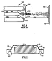
- FIG. 2 shows a cross-sectional view of a gas ring for a plasma etching apparatus according to an exemplary embodiment of the invention.
- FIG. 3 shows an etch chamber containing exemplary embodiments of components according to the invention.
- FIG. 4 shows another etch chamber containing exemplary embodiments of components according to the invention.
- FIG. 5 shows an exemplary embodiment of a protective coating according to the invention.
- FIG. 6 shows another exemplary embodiment of a protective coating according to the invention.
- the invention provides components suitable for use in semiconductor material processing apparatuses.
- the components can provide wear resistance with respect to physical and chemical attack by plasmas generated in semiconductor material processing apparatuses during processing.
- wear resistant includes, but is not limited to, resistance to erosion, corrosion and/or corrosion-erosion.
- the components comprise a yttrium oxide (yttria)-containing coating.
- yttria-containing coating provides an outer surface resistant to chemical and/or physical attack by plasmas in apparatuses for processing semiconductors, which outer or outermost surface is facing to the interior of the apparatus for processing semiconductors.
- the invention provides methods of making components that comprise the yttria-containing coatings to enhance the wear resistance of the components in plasma environments.
- wear resistant materials can be applied to different processing apparatuses useful for processing different semiconductor materials.
- the wear resistant materials can be applied to different components in the processing apparatuses.
- Such exemplary components include, but are not limited to, parts of a plasma and/or vacuum chamber, such as, for example, chamber walls, substrate supports, gas distribution systems including showerheads, baffles, rings, nozzles, etc., fasteners, heating elements, plasma screens, liners, transport module components, such as robotic arms, fasteners, inner and outer chamber walls, and the like.
- the yttria-containing coatings can provide a high bond strength to the underlying substrate.
- the yttria-containing coatings have a tensile bond strength of from about 13.79 MPa to about 48.265 MPa (2000 psi to about 7000 psi).
- the yttria-containing coatings can provide low porosity levels, which is advantageous to minimize contact of aggressive atmospheres with the underlying substrate, and thus subsequent physical and/or chemical attack by corrosion, erosion and/or corrosion-erosion of the substrate by the aggressive atmosphere.
- the yttria-containing coatings have a porosity of less than 15% by volume, more preferably less than about 3% by volume, and most preferably less than about 1% by volume.
- the yttria-containing coatings can provide a high hardness to resist erosion.
- the ceramic materials have a hardness (HVO 3 ) of from about 200 to about 800.
- the yttria-containing coatings have a crystal structure that is preferably from about 10% to about 100% cubic, and more preferably more than about 95% cubic.
- the yttria-containing coatings can provide desirable wear resistance properties for use in semiconductor processing apparatus, such as, e.g., plasma etch chambers.
- the yttria-containing coatings provide surfaces that can reduce ion induced erosion and associated levels of particulate contamination in plasma reactor chambers.
- the yttria-containing coatings can protect underlying substrates against both physical attack and chemical attack by plasmas.
- the wear resistant coatings can be used in various different plasma atmospheres for etching, deposition, as well as other applications.
- Typical etch chemistries include, for example, chlorine containing gases including, but not limited to, Cl 2 , HCl and BCl 3 ; bromine containing gases including, but not limited to, Br 2 and HBr; oxygen containing gases including, but not limited to, O 2 , H 2 O and SO 2 ; fluorine containing gases including, but not limited to, CF 4 , CH 2 F 2 , NF 3 , CH 3 F, C 2 F 6 , CHF 3 and SF 6 ; and inert and other gases including, but not limited to He, Ar and N 2 .
- Exemplary plasma etch reactor etching operating conditions for a high density plasma reactor are as follows: substrate temperature of from about 0°C to about 70°C; chamber pressure of from about 0 Pa to about 13.33 Pa (0 mTorr to about 100 mTorr); gas flow rate of from about 10 sccm to about 1000 sccm; and plasma generating power of from more than 0 Watts to about 1500 Watts, and typically from about 200 Watts to about 800 Watts.
- the power that is most suitable is dependent on the type of wafer that is etched in the plasma reactor.
- the yttria-containing coatings are preferably formed on substrates by a thermal spraying technique.
- thermal spraying techniques ceramic powder is melted and incorporated in a gas stream directed at the component being spray coated.
- An advantage of thermal spraying techniques is that the component is coated only on the sides facing the thermal spray gun, and masking can be used to protect other areas.
- Conventional thermal spraying techniques, including plasma spraying, are described in The Science and Engineering of Thermal Spray Coating by Pawlowski (John Wiley, 1995 ).
- the thermal sprayed yttria-containing coatings can be formed on any substrates that are suitably shaped to enable them to be coated.
- the electric arc extends down the nozzle.
- the powder 112 is so rapidly heated and accelerated that the spray distance 136 between the nozzle tip and the substrate surface can advantageously be on the order of 125 to 150 mm.
- Plasma sprayed coatings are produced by molten or heat-softened particles impacting on the substrate surface 116.
- the thermal sprayed yttria-containing coatings can be formed directly on preferred substrate materials with or without having previously treated the substrate surface to promote adhesion of the coatings, and/or with or without having previously formed intermediate coatings on the substrate to enhance adhesion of the coatings on the substrates.
- the yttria-containing coatings can be applied directly to anodized aluminum, alumina or quartz substrates without treating the substrate surface or utilizing intermediate coatings.
- the yttria-containing coatings provide suitable adherence to the substrates without treating the substrate and/or forming intermediate layers. Accordingly, because the yttria-containing coatings can be applied to substrates without performing such additional prior process steps, the increased cost, complexity and/or completion time of the coating process contributed to such additional process steps can be avoided.
- the substrate surface to be coated Prior to forming the yttria-containing coatings on substrates, the substrate surface to be coated is preferably cleaned to remove undesirable surface substances, such as oxides or grease.
- surface treating techniques such as cleaning and particle blasting, can be used to provide a more chemically and physically active surface for bonding of the coating.
- the surface of substrate can be roughened by any suitable method, such as grit blasting, prior to coating. Roughening of the substrate increases the surface area available for bonding of the coating, which increases the coating bond strength.
- the rough substrate surface profile can also promote mechanical keying or interlocking of the coating with the substrate.
- the surface of the component that is to be coated is anodized prior to coating .
- the anodized layer provides an additional barrier, i.e., in addition to the protection provided by the coating, against corrosive attack of the underlying aluminum material.
- the anodized aluminum layer formed on aluminum substrates, such as 6061-T6 aluminum can have any suitable thickness.
- the anodized aluminum layer thickness can typically be from about 50.8 ⁇ m to about 254 ⁇ m (2 mil to about 10 mil).
- the surface of the anodized aluminum layer can have any suitable finish.
- the surface finish can advantageously have a surface roughness of about 0.508 ⁇ m to about 2.54 ⁇ m (20 to about 100 micro-inch).
- the anodized layer is sealed by any suitable technique, such as by using boiling deionized water. deionized water.
- the thermal sprayed yttria-containing coatings can have desired surface roughness characteristics effective to promote the adhesion of contaminants to the coatings.
- the contaminants can include polymer deposits, which result from the use of polymer forming species (usually fluorocarbons) during plasma etching processes, such as metal etching processes. As described in co-pending U.S. Patent Application No. 09/749,917 , such polymer deposits can flake or peel off of chamber surfaces during etching processes and contaminate substrates within the chamber. The thermal cycling that occurs during repeated plasma processing cycles exacerbates this problem.
- the thermal sprayed yttria-containing coatings can have surface roughness values (Ra) suitable for enhancing adhesion of polymer byproducts produced during processing of substrates in the plasma reactor.
- the arithmetic mean surface roughness (Ra) of the thermal sprayed yttria-containing coatings can range from about 0.127 ⁇ m to about 10.16 ⁇ m (5 to about 400 micro-inches), and preferably from about 3.048 ⁇ m to about 6.35 ⁇ m (120 to about 250 micro-inches).
- Surface roughness values in this range promote the adhesion of polymer deposited on interior surfaces of the reaction chamber during a plasma etch process, such as a metal etch. Accordingly, the thermal sprayed yttria-containing coatings can improve the adhesion of such polymer deposits on components, and thereby reduce the occurrence of contamination by the polymer deposits.
- the thermal sprayed yttria-containing coatings can be smooth.
- the thermal sprayed yttria-containing coatings can have rough surfaces to promote adhesion of the deposits on the coatings.
- smoother surfaces are relatively easy to clean.
- the components including a yttria-containing coating are used in a high-density plasma reactor.
- An exemplary reactor of this type is the TCP 9400 TM plasma etch reactor available from Lam Research Corporation of Fremont, California.
- processing gases such as Cl 2 , HBr, CF 4 , CH 2 F 2 , O 2 , N 2 , Ar, SF 6 and NF 3 ) are conducted into a gas ring located at the bottom of the etch chamber and are then guided through gas holes into the reactor chamber.
- FIG. 2 shows a gas ring for a TCP 9400 TM etch reactor.
- the main body of the gas ring 40 surrounds a substrate support 44.
- the bottom surface of the gas ring 40 contains a ring-shaped gas-guiding trench 60.
- the aforementioned gas holes 50 extend into the gas-guiding trench 60.
- the gas ring 40 is typically composed of aluminum. Upper surfaces of the gas ring are directly exposed to the plasma and thus subject to erosion, corrosion and corrosion-erosion. To protect these surfaces, the gas ring is typically covered with an aluminum oxide layer. For example, in silicon etch applications, fluorine-containing atmospheres can produce aluminum fluoride "brown dust" by attacking anodized aluminum. In metal etch applications, boron trichloride (BCl 3 ) can etch away the anodized aluminum surface, resulting in corrosion of components. In addition, anodized aluminum is relatively brittle and can crack during repeated thermal cycling of the reactor during use. Cracks that form in the anodized layer can allow the corrosive process gases to attack the underlying aluminum layer, reducing part life and contributing to metallic and particle contamination of processed substrates, such as wafers, flat panel display substrates and the like.
- the exposed surfaces of the gas ring is covered with a coating 42 of a yttria-containing material.
- the coatings is formed on aluminum having an anodized surface.
- the coating can be allowed to partially penetrate into the gas holes to coat and protect the inside walls thereof, but without obstructing the openings.
- the gas holes can be uncoated, e.g., the gas holes can be plugged or masked during the coating process.
- TCP 9400 TM etch reactor that can be exposed to the plasma during processing can also be coated with a yttria-containing coating.
- these components include, for example, chamber walls, chamber liners, chucking devices and the dielectric window opposite the substrate.
- Providing a yttria-containing coating on the upper surface of a chucking device, such as an electrostatic chuck, provides additional protection to the chuck during cleaning cycles in which a wafer is not present and the upper surface of the chuck is thus directly exposed to the plasma.
- the reactor comprises a reactor chamber 150 that includes a substrate support 152 including an electrostatic chuck 154, which provides a clamping force to a substrate (not shown) mounted thereon.
- a focus ring 170 is mounted on the substrate support 152 around the electrostatic chuck 154.
- the substrate support 152 can also be used to apply an RF bias to the substrate.
- the substrate can also be back-cooled using a heat transfer gas such as helium.
- processing gases e.g., one or more of Cl 2 , HBr, CF 4 , CH 2 F 2 , O 2 , N 2 , Ar, SF 6 or NF 3
- gases e.g., one or more of Cl 2 , HBr, CF 4 , CH 2 F 2 , O 2 , N 2 , Ar, SF 6 or NF 3
- the gas injector 168 is typically made of quartz or a ceramic material such as alumina.
- an inductive coil 158 can be powered by a suitable RF source (not shown) to provide a high density (e.g., 10 11 - 10 12 ions/cm 3 ) plasma.
- the inductive coil 158 couples RF energy through dielectric window 160 into the interior of chamber 150.
- the dielectric window 160 is typically made of quartz or alumina.
- the dielectric window 160 is shown mounted on an annular member 162.
- the annular member 162 spaces dielectric window 160 from the top of chamber 150 and is referred to as a "gas distribution plate".
- a chamber liner 164 surrounds the substrate support 152.
- the chamber 150 can also include suitable vacuum pumping apparatus (not shown) for maintaining the interior of the chamber at a desired pressure.
- FIG. 3 selected internal surfaces of reactor components, such as the annular member 162, dielectric window 160, substrate support 152, chamber liner 164, gas injector 168, focus ring 170 and the electrostatic chuck 154, are shown coated with a yttria-containing coating 166 according to the invention.
- a yttria-containing coating 166 As shown in FIG. 3 , selected interior surfaces of the chamber 150 and substrate support 152 below the chamber liner 164 can also be provided with a yttria-containing coating 166. Any or all of these surfaces, as well as any other internal reactor surface, can be provided with a yttria-containing coating.
- the components can be used in a high-density oxide etch process.
- An exemplary oxide etch reactor is the TCP 9100 TM plasma etch reactor available from Lam Research Corporation of Fremont, California.
- the gas distribution plate is a circular plate situated directly below the TCP TM window, which is also the vacuum sealing surface at the top of the reactor in a plane above and parallel to a semiconductor wafer.
- the gas distribution plate is sealed to a gas distribution ring located at the periphery of the gas distribution plate.
- the gas distribution ring feeds gas from a gas source into the volume defined by the gas distribution plate, an inside surface of a window underlying an antenna in the form of a flat spiral coil supplying RF energy into the reactor, and the gas distribution ring.
- the gas distribution plate contains holes of a specified diameter, which extend through the plate.
- the spatial distribution of the holes through the gas distribution plate can be varied to optimize etch uniformity of the layers to be etched, e.g., a photoresist layer, a silicon dioxide layer and an underlayer material on the wafer.
- the cross-sectional shape of the gas distribution plate can be varied to manipulate the distribution of RF power into the plasma in the reactor.
- the gas distribution plate is a dielectric material to enable coupling of this RF power through the gas distribution plate into the reactor. Further, it is desirable for the material of the gas distribution plate to be highly resistant to chemical sputter-etching in environments, such as oxygen, halogen or hydro-fluorocarbon gas plasma, to avoid breakdown and the resultant particle generation associated therewith.
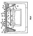
- FIG. 4 illustrates a plasma reactor of the aforementioned type.
- the reactor comprises a reactor chamber 10.
- a substrate holder 12 includes an electrostatic chuck 34, which provides a clamping force and an RF bias to a substrate 13.
- the substrate can be back-cooled using a heat transfer gas such as helium.
- a focus ring 14 confines plasma in a region above the substrate.
- the reactor chamber includes a vacuum pumping apparatus for maintaining the interior of the chamber at a desired pressure (e.g., below 6.665 Pa [50 mTorr], typically 0.1333-2.666 Pa [1-20 mTorr]).
- a substantially planar dielectric window 20 is provided between the antenna 18 and the interior of the processing chamber 10 and forms the vacuum wall at the top of the processing chamber 10.
- a gas distribution plate 22 is provided beneath window 20 and includes openings for delivering process gas from the gas supply 23 to the chamber 10.
- a liner 30, such as a conical or cylindrical liner, extends from the gas distribution plate 22 and surrounds the substrate holder 12.
- the antenna 18 can be provided with a channel 24 through which a temperature control fluid is flowed via inlet and outlet conduits 25, 26.
- the antenna 18 and/or window 20 need not be cooled, or could be cooled by other suitable technique, such as by blowing gas over the antenna and window, passing a cooling fluid through or in heat transfer contact with the window and/or gas distribution plate, etc.
- the exposed internal surfaces of reactor components such as the gas distribution plate 22, the chamber liner 30, the electrostatic chuck 34, and the focus ring 14 are coated with a yttria-containing coating 32.
- a yttria-containing coating 32 only selected ones of these surfaces, and/or other surfaces, can be coated with a yttria-containing coating.
- the high density polysilicon and dielectric etch chambers described above are only exemplary embodiments of plasma etch reactors that can incorporate the components.
- Components including a yttria-containing coating can be used in any etch reactor (e.g., a metal etch reactor) or other type of semiconductor processing apparatus where the reduction of plasma induced erosion, corrosion and/or corrosion-erosion and associated contamination is desired.
- exemplary components that can be provided with a yttria-containing coating include, but are not limited to, chamber walls, substrate holders, fasteners, etc. These components are typically made from metal (e.g., aluminum) or ceramic (e.g., alumina), and are typically exposed to plasma and often show signs of erosion, corrosion and/or corrosion-erosion. Other parts that can be coated with a yttria-containing coating need not be directly exposed to plasma, but may instead be exposed to corrosive gases, such as gases emitted from processed wafers or the like. Therefore, other equipment used in processing semiconductor substrates can also be provided with yttria-containing coatings. Such equipment can include transport mechanisms, gas supply systems, liners, lift mechanisms, load locks, door mechanisms, robotic arms, fasteners, and the like.
- a yttria-containing coating is provided on a metallic component.
- anodized or non-anodized aluminum-based materials including aluminum and aluminum alloys, e.g., 6061-T6 aluminum, can be coated with yttria-containing coatings.
- Other exemplary metallic materials that can be coated include, but are not limited to, stainless steels and refractory metals, e.g., 304 and 316 stainless steels. Because the yttria-containing coatings form a wear resistant coating over the component, the underlying component is protected from direct exposure to the plasma. Accordingly, the metallic component can be protected against erosion, corrosion and/or corrosion-erosion attack by the plasma.
- metallic materials such as aluminum alloys, can be used without regard to alloying additions, grain structure or surface conditions.
- the reactor components can be made from ceramic materials, including, but not limited to, alumina (Al 2 O 3 ), silicon carbide (SiC), silicon nitride (Si 3 N 4 ), boron carbide (B 4 C) and/or boron nitride (BN).
- Ceramic materials that can be coated are preferably those that can withstand elevated temperature conditions present in plasma reactors.
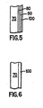
- FIG. 5 shows a coated component according to an example.
- a first intermediate coating 80 is optionally coated on a substrate 70 by a conventional technique.
- the optional first intermediate coating 80 is sufficiently thick to adhere to the substrate and to further allow it to be processed prior to forming an optional second intermediate coating 90, or the yttria-containing coating 100.
- the first intermediate coating 80 and the second intermediate coating 90 can have any suitable thickness that provides these desired properties.
- These coatings can have a thickness of at least about 0.0254 mm (0.001 inch), preferably from about 0.0254 mm to about 6.35 mm (0.001 inch to about 0.25 inch), more preferably from about 0.0254 mm to about 3.81 mm (0.001 inch to about 0.15 inch), and most preferably from about 0.0254 mm to about 1.27 mm (0.001 inch to about 0.05 inch).
- the first intermediate coating can be treated, such as by roughening using any suitable technique, and then coated with the optional second intermediate coating 90, or with the yttria-containing coating 100.
- a roughened first intermediate coating 80 provides a particularly good bond to subsequently applied coatings.
- the second intermediate coating 90 imparts a high mechanical compression strength to the first intermediate coating 80 and reduces formation of fissures in the second intermediate coating 90.
- the second intermediate coating 90 is sufficiently thick to adhere to the first intermediate coating 80 and to allow it to be processed prior to forming any additional intermediate coatings, or the outer yttria-containing coating 100.
- the second intermediate coating 90 also can be treated, such as by roughening.
- the second intermediate coating 90 can have any suitable thickness that provides these desired properties, such as a thickness of at least about 0.0254 mm (0.001 inch), preferably from about 0.0254 mm to about 6.35 mm (0.001 inch to about 0.25 inch), more preferably from about 0.0254 mm to about 3.81 mm (0.001 inch to about 0.15 inch), and most preferably from about 0.0254 mm to about 1.27 mm (0.001 inch to about 0.05 inch).
- the first and second intermediate coatings can be made of any metallic, ceramic and polymer materials that are suitable for use in semiconductor plasma processing chambers.
- Particularly desirable metals that can be used include, but are not limited to, refractory metals, which can withstand high processing temperatures.
- Preferred ceramics include, but are not limited to, Al 2 O 3 , SiC, Si 3 N 4 , B 4 C, AlN, TiO 2 and mixtures thereof.
- Preferred polymers include, but are not limited to, fluoropolymers, such as polytetrafluoroethylene and polyimides.
- the intermediate coatings can be applied by any suitable deposition technique such as plating (e.g., electroless plating or electroplating), sputtering, immersion coating, chemical vapor deposition, physical vapor deposition, electrophoretic deposition, hot isostatic pressing, cold isostatic pressing, compression molding, casting, compacting and sintering, and thermal spraying (e.g., plasma spraying).
- plating e.g., electroless plating or electroplating
- sputtering immersion coating
- chemical vapor deposition e.g., physical vapor deposition
- electrophoretic deposition e.g., hot isostatic pressing, cold isostatic pressing, compression molding, casting, compacting and sintering
- thermal spraying e.g., plasma spraying
- the optional first intermediate coating 80 and second intermediate coating 90 can have the same or different compositions from each other, depending on their desired properties. If desired, additional intermediate coatings such as a third, fourth or fifth intermediate coating of the same or different materials can also be provided between the yttria-containing coating and the substrate.
- FIG. 6 shows another embodiment of the yttria-containing coatings.
- the yttria-containing coating 100 is deposited directly onto a substrate (i.e., without the formation any intermediate layers), which is an outer surface of the component 70.
- the coating 100 can have any suitable thickness.
- the yttria-containing coating 100 has at least a minimum thickness that provides sufficient coverage of the underlying surface to provide wear resistance and protect the underlying surface against physical and chemical attack, when the yttria-containing coating is exposed to plasma atmospheres.
- the coating 100 can have a thickness in the range of about 0.0254 mm to about 25.4 mm (0.001 inch to about 1 inch), preferably from about 0.0254 mm to about 12.7 mm (0.001 inches to about 0.5 inch), more preferably from about 0.0254 mm to about 2.54 mm (0.001 inch to about 0.1 inch), and most preferably from about 0.254 mm to about 2,54 mm (0.01 inch to about 0.1 inch).
- This thickness can also be used in other embodiments.
- the thickness of the yttria-containing coating can be selected to be compatible with the plasma environment to be encountered in the reactor (e.g., etching, CVD, etc.).
- the yttria-containing coatings can be provided on all or part of the reactor chamber and components.
- the coatings are provided on the regions of the reactor chamber that are exposed to the plasma environment, such as those parts in direct contact with the plasma, or parts located behind chamber components, such as liners. Additionally, it is preferred that the yttria-containing coating be provided at regions of the reactor chamber that are subjected to relatively high bias voltages (i.e. relatively high sputter ion energies).
- the yttria-containing coatings can be used for all plasma chemistries.
- the coatings are advantageous for use in fluorine-containing and BCl 3 containing-atmospheres, which are highly erosive to anodized aluminum.
- Tests were conducted to demonstrate the effectiveness of the yttria-containing coatings in providing an erosion resistant surface in a plasma environment.
- Three anodized 6061-T6 aluminum coupons and three coupons each made by forming a thermal sprayed yttria-containing coating on a surface of an anodized 6061-T6 aluminum coupon were attached to a chamber wall in a plasma reactor chamber.
- the yttria-containing coatings had a composition of about 99.95 wt.% yttria.
- the coupons each had a 25.4 mm, (1 inch) diameter and a thickness of 3.525 mm (0.375 inch). The coupons were attached to the chamber wall.
- a plasma was generated from a process gas comprising Cl 2 and BCl 3 at equal flow rates, and the interior of the chamber was set to a pressure of 0.7998 Pa (6 mTorr). Bare silicon wafers were etched in the reactor chamber. The coupons were tested for a total of about 90 RF-hours.
- the three coupons having a yttria-containing coating each gained weight due to the accumulation of dust on the coatings.
- the weight gain of the three coated coupons ranged from about 0.8 mg to about 1.2 mg.
- the anodized 6061-T6 aluminum coupons without a yttria-containing coating significantly eroded, as evidenced by the significant weight loss. These coupons were determined to have an estimated average erosion rate of from about 2.0 to 2.7 nm/RF-min (20 to 27 ⁇ /RF-min). In contrast, the three coupons having a yttria-containing coating were not eroded.
- the yttria-containing coatings can minimize or even prevent the formation of aluminum fluoride when coated components are used in a fluorine-containing process gas atmosphere in a plasma reactor.
- Tests were also performed to demonstrate the reduction of contamination of wafers during etching in a plasma reactor by providing components in the plasma reactor chamber that include a thermal sprayed yttria-containing coating, which consists essentially of yttria. Tests were performed on a 9400DFM plasma reactor with a chamber liner fully encapsulated with a yttria-containing coating, a ground ring coated with a yttria-containing coating, ground ring screw caps coated with a yttria-containing coating, and a quartz window in the reactor chamber.
- the reactor chamber was prepared by a procedure including a wet clean with 6% H 2 O + isopropyl alcohol wipe down, and a wet clean recovery procedure using six oxide wafers and the following process parameters: 3.3325 Pa (15mT) chamber pressure/800 Watts top coil power/O W bottom electrode power/100 sccm SF 6 /20 sccm Cl 2 /50 sccm O 2 /1066.4 Pa (8 Torr) He back cool /300 sec etch time.
- Conditioning of the reactor chamber was performed using ten bare silicon wafers with the following process parameters: break through etch: 0.5332 Pa (4 mTorr) chamber pressure/600 Watts top coil power/65 Watts bottom electrode power/100 sccm HBr/10 sec etch time; main etch: 0.7998 Pa (6 mTorr) chamber pressure/350 Watts top coil power/20 Watts bottom electrode power/180 sccm HBr/65 sec etch time; and over etch: 10.664 Pa (80 mT) chamber pressure/350 Watts top coil power/75 Watts bottom electrode power/150 sccm HBr/150 sccm He/5 sccm O 2 /90 sec etch time. High pressure waferless autocleaning was used after every wafer.
- a 100 nm (1 k ⁇ ) thermal oxide wafer was etched with the following process parameters: break through etch: 0.5332 Pa (4 mTorr) chamber pressure/600 Watts top coil power/65 Watts bottom electrode power/100 sccm HBr/10 sec etch time; main etch: 0.7998 Pa (6 mTorr) chamber pressure/350 Watts top coil power/20 Watts bottom electrode power/180 sccm HBr/65 sec etch time; and over etch: 10.664 Pa (80 mTorr) chamber pressure/350 top coil power/75 Watts bottom electrode power/150 sccm HBr/150 sccm He/5 sccm O 2 /90 sec etch time.
- the silicon wafers were etched using the following process parameters: 0.6665 Pa (5 mT) chamber pressure/250 Watts top coil powder/150 Watts bottom electrode power/50 sccm Cl 2 /120 sec etch time. Following etching, the thermal oxide wafers and the prime silicon wafers were analyzed for contamination using ICP-MS.
- Thermal oxide wafers and bare silicon wafers were placed in the reactor chamber and etched using the above-described process parameters with and without components including a yttria-containing coating being present in the reactor Following etching, the surface concentration of Al, Cr, Cu, Fe, Ni, Na and Y was measured in units of 10 10 atoms/cm 2 for the wafers.
- FIG. 7 shows the results for the contamination analysis of the wafers.
- "Coated” means yttria-coated components were present in the reactor chamber and "uncoated” means yttria-coated components were not present. Comparing the test results for the same wafer type, i.e., thermal oxide wafers and bare silicon wafers, the test results show that on an element-by-element basis, the results for reactor chamber including yttria-coated components was significantly lower than for the reactor chamber containing plasma exposed anodized aluminum surfaces on components.
- the aluminum concentration measured for the "uncoated" bare silicon wafer was about 87 x 10 10 atoms/cm 2
- the aluminum concentration measured for the "coated” bare silicon wafer was about 12 x 10 10 atoms/cm 2
- the chromium concentration measured for the "uncoated” bare silicon wafer was about 7 x 10 10 atoms/cm 2
- the chromium concentration measured for the "coated” bare silicon wafer was about 10 9 atoms/cm 2 , which was the detection limit of the measuring equipment.
- the yttria or yttrium levels were insignificant for all of the wafers tested.
- no yttria was detected above the detection limits of the measuring equipment.
- the results demonstrate the robust nature of the yttria-containing coatings in the plasma environment. Consequently, the yttria-containing coatings can achieve very low levels of on-wafer yttria contamination.
- the yttria-containing coatings can provide an extremely hard, wear resistant surface. Such coatings are desirably free of materials that react with processing chamber gases, and are chemically inert such that there is low or no particle contamination, minimal or no corrosion, minimal or no metal contamination and/or minimal or no volatile etch products. Thus, the yttria-containing coatings can decrease levels of metal and particulate contamination, lower costs by increasing the lifetime of consumables, decrease process drifts and reduce the levels of corrosion of chamber parts and substrates.
Landscapes
- Chemical & Material Sciences (AREA)
- Engineering & Computer Science (AREA)
- Physics & Mathematics (AREA)
- Plasma & Fusion (AREA)
- Analytical Chemistry (AREA)
- Organic Chemistry (AREA)
- General Physics & Mathematics (AREA)
- Materials Engineering (AREA)
- Mechanical Engineering (AREA)
- Metallurgy (AREA)
- General Chemical & Material Sciences (AREA)
- Condensed Matter Physics & Semiconductors (AREA)
- Chemical Kinetics & Catalysis (AREA)
- Manufacturing & Machinery (AREA)
- Computer Hardware Design (AREA)
- Microelectronics & Electronic Packaging (AREA)
- Power Engineering (AREA)
- Drying Of Semiconductors (AREA)
- Coating By Spraying Or Casting (AREA)
- Plasma Technology (AREA)
Applications Claiming Priority (3)
| Application Number | Priority Date | Filing Date | Title |
|---|---|---|---|
| US180504 | 2002-06-27 | ||
| US10/180,504 US7311797B2 (en) | 2002-06-27 | 2002-06-27 | Productivity enhancing thermal sprayed yttria-containing coating for plasma reactor |
| PCT/US2003/018502 WO2004003962A2 (en) | 2002-06-27 | 2003-06-12 | Thermal sprayed yttria-containing coating for plasma reactor |
Publications (2)
| Publication Number | Publication Date |
|---|---|
| EP1518255A2 EP1518255A2 (en) | 2005-03-30 |
| EP1518255B1 true EP1518255B1 (en) | 2012-02-08 |
Family
ID=29778939
Family Applications (1)
| Application Number | Title | Priority Date | Filing Date |
|---|---|---|---|
| EP03737030A Expired - Lifetime EP1518255B1 (en) | 2002-06-27 | 2003-06-12 | Thermal sprayed yttria-containing coating for plasma reactor |
Country Status (9)
| Country | Link |
|---|---|
| US (2) | US7311797B2 (zh:) |
| EP (1) | EP1518255B1 (zh:) |
| JP (2) | JP2005531157A (zh:) |
| KR (2) | KR101107542B1 (zh:) |
| CN (1) | CN1663017A (zh:) |
| AT (1) | ATE545148T1 (zh:) |
| AU (1) | AU2003238006A1 (zh:) |
| TW (1) | TWI328411B (zh:) |
| WO (1) | WO2004003962A2 (zh:) |
Families Citing this family (235)
| Publication number | Priority date | Publication date | Assignee | Title |
|---|---|---|---|---|
| KR20010062209A (ko) | 1999-12-10 | 2001-07-07 | 히가시 데쓰로 | 고내식성 막이 내부에 형성된 챔버를 구비하는 처리 장치 |
| US6805952B2 (en) * | 2000-12-29 | 2004-10-19 | Lam Research Corporation | Low contamination plasma chamber components and methods for making the same |
| US7416625B2 (en) * | 2001-03-29 | 2008-08-26 | Bridgestone Corporation | Rubber strip, method for manufacturing tire and tire component member using same, and apparatus therefor |
| US7371467B2 (en) * | 2002-01-08 | 2008-05-13 | Applied Materials, Inc. | Process chamber component having electroplated yttrium containing coating |
| US8067067B2 (en) * | 2002-02-14 | 2011-11-29 | Applied Materials, Inc. | Clean, dense yttrium oxide coating protecting semiconductor processing apparatus |
| US7166166B2 (en) * | 2002-09-30 | 2007-01-23 | Tokyo Electron Limited | Method and apparatus for an improved baffle plate in a plasma processing system |
| US6798519B2 (en) * | 2002-09-30 | 2004-09-28 | Tokyo Electron Limited | Method and apparatus for an improved optical window deposition shield in a plasma processing system |
| US7166200B2 (en) | 2002-09-30 | 2007-01-23 | Tokyo Electron Limited | Method and apparatus for an improved upper electrode plate in a plasma processing system |
| US6837966B2 (en) * | 2002-09-30 | 2005-01-04 | Tokyo Electron Limeted | Method and apparatus for an improved baffle plate in a plasma processing system |
| US7204912B2 (en) | 2002-09-30 | 2007-04-17 | Tokyo Electron Limited | Method and apparatus for an improved bellows shield in a plasma processing system |
| US7137353B2 (en) * | 2002-09-30 | 2006-11-21 | Tokyo Electron Limited | Method and apparatus for an improved deposition shield in a plasma processing system |
| US7147749B2 (en) * | 2002-09-30 | 2006-12-12 | Tokyo Electron Limited | Method and apparatus for an improved upper electrode plate with deposition shield in a plasma processing system |
| TW200423195A (en) | 2002-11-28 | 2004-11-01 | Tokyo Electron Ltd | Internal member of a plasma processing vessel |
| US20060226003A1 (en) * | 2003-01-22 | 2006-10-12 | John Mize | Apparatus and methods for ionized deposition of a film or thin layer |
| CN100418187C (zh) * | 2003-02-07 | 2008-09-10 | 东京毅力科创株式会社 | 等离子体处理装置、环形部件和等离子体处理方法 |
| DE602004009982T2 (de) * | 2003-03-31 | 2008-09-18 | Sanyo Electric Co., Ltd., Moriguchi | Metallschablone und Verfahren zum Drucken von bleifreier Lötpaste mit derselben |
| WO2004095530A2 (en) * | 2003-03-31 | 2004-11-04 | Tokyo Electron Limited | Adjoining adjacent coatings on an element |
| JP4532479B2 (ja) | 2003-03-31 | 2010-08-25 | 東京エレクトロン株式会社 | 処理部材のためのバリア層およびそれと同じものを形成する方法。 |
| US7297247B2 (en) * | 2003-05-06 | 2007-11-20 | Applied Materials, Inc. | Electroformed sputtering target |
| US6843870B1 (en) * | 2003-07-22 | 2005-01-18 | Epic Biosonics Inc. | Implantable electrical cable and method of making |
| US7220497B2 (en) * | 2003-12-18 | 2007-05-22 | Lam Research Corporation | Yttria-coated ceramic components of semiconductor material processing apparatuses and methods of manufacturing the components |
| US8213467B2 (en) | 2004-04-08 | 2012-07-03 | Sonosite, Inc. | Systems and methods providing ASICs for use in multiple applications |
| CN1690254B (zh) * | 2004-04-13 | 2013-03-13 | 应用材料有限公司 | 具有含电镀钇涂层的制程腔室构件 |
| US7119032B2 (en) | 2004-08-23 | 2006-10-10 | Air Products And Chemicals, Inc. | Method to protect internal components of semiconductor processing equipment using layered superlattice materials |
| US8017062B2 (en) * | 2004-08-24 | 2011-09-13 | Yeshwanth Narendar | Semiconductor processing components and semiconductor processing utilizing same |
| JP2006186306A (ja) * | 2004-09-30 | 2006-07-13 | Toshiba Ceramics Co Ltd | ガス拡散プレートおよびその製造方法 |
| US7226869B2 (en) * | 2004-10-29 | 2007-06-05 | Lam Research Corporation | Methods for protecting silicon or silicon carbide electrode surfaces from morphological modification during plasma etch processing |
| US7552521B2 (en) | 2004-12-08 | 2009-06-30 | Tokyo Electron Limited | Method and apparatus for improved baffle plate |
| WO2006064898A1 (ja) * | 2004-12-17 | 2006-06-22 | Tokyo Electron Limited | プラズマ処理装置 |
| US7601242B2 (en) | 2005-01-11 | 2009-10-13 | Tokyo Electron Limited | Plasma processing system and baffle assembly for use in plasma processing system |
| US9659758B2 (en) | 2005-03-22 | 2017-05-23 | Honeywell International Inc. | Coils utilized in vapor deposition applications and methods of production |
| JP2006319043A (ja) * | 2005-05-11 | 2006-11-24 | Hitachi High-Technologies Corp | プラズマ処理装置 |
| CN101218376A (zh) * | 2005-06-17 | 2008-07-09 | 国立大学法人东北大学 | 金属构件的保护膜构造及采用该保护膜构造的金属零件、半导体或平板显示器制造装置 |
| US20090194233A1 (en) * | 2005-06-23 | 2009-08-06 | Tokyo Electron Limited | Component for semicondutor processing apparatus and manufacturing method thereof |
| JP4813115B2 (ja) * | 2005-07-14 | 2011-11-09 | 国立大学法人東北大学 | 半導体製造装置用部材及びその洗浄方法 |
| US7976641B1 (en) * | 2005-09-30 | 2011-07-12 | Lam Research Corporation | Extending storage time of removed plasma chamber components prior to cleaning thereof |
| CN101305451B (zh) * | 2005-11-08 | 2012-07-04 | 国立大学法人东北大学 | 簇射极板及采用该簇射极板的等离子体处理装置 |
| US20070108161A1 (en) * | 2005-11-17 | 2007-05-17 | Applied Materials, Inc. | Chamber components with polymer coatings and methods of manufacture |
| JP4856978B2 (ja) * | 2006-02-21 | 2012-01-18 | 株式会社日立ハイテクノロジーズ | プラズマエッチング装置及び処理室の内壁の形成方法 |
| US20070215278A1 (en) * | 2006-03-06 | 2007-09-20 | Muneo Furuse | Plasma etching apparatus and method for forming inner wall of plasma processing chamber |
| JP5014656B2 (ja) * | 2006-03-27 | 2012-08-29 | 国立大学法人東北大学 | プラズマ処理装置用部材およびその製造方法 |
| US7906032B2 (en) * | 2006-03-31 | 2011-03-15 | Tokyo Electron Limited | Method for conditioning a process chamber |
| US7655328B2 (en) * | 2006-04-20 | 2010-02-02 | Shin-Etsu Chemical Co., Ltd. | Conductive, plasma-resistant member |
| US20070246795A1 (en) * | 2006-04-20 | 2007-10-25 | Micron Technology, Inc. | Dual depth shallow trench isolation and methods to form same |
| US7884026B2 (en) * | 2006-07-20 | 2011-02-08 | United Microelectronics Corp. | Method of fabricating dual damascene structure |
| US20080029032A1 (en) * | 2006-08-01 | 2008-02-07 | Sun Jennifer Y | Substrate support with protective layer for plasma resistance |
| CN101123214B (zh) * | 2006-08-07 | 2011-03-16 | 联华电子股份有限公司 | 双镶嵌结构的制作方法 |
| JPWO2008032627A1 (ja) * | 2006-09-11 | 2010-01-21 | 株式会社アルバック | ドライエッチング方法 |
| US7838800B2 (en) * | 2006-09-25 | 2010-11-23 | Tokyo Electron Limited | Temperature controlled substrate holder having erosion resistant insulating layer for a substrate processing system |
| US7723648B2 (en) * | 2006-09-25 | 2010-05-25 | Tokyo Electron Limited | Temperature controlled substrate holder with non-uniform insulation layer for a substrate processing system |
| JP2008103403A (ja) * | 2006-10-17 | 2008-05-01 | Tokyo Electron Ltd | 基板載置台及びプラズマ処理装置 |
| US8702866B2 (en) * | 2006-12-18 | 2014-04-22 | Lam Research Corporation | Showerhead electrode assembly with gas flow modification for extended electrode life |
| US8097105B2 (en) * | 2007-01-11 | 2012-01-17 | Lam Research Corporation | Extending lifetime of yttrium oxide as a plasma chamber material |
| US20080196661A1 (en) * | 2007-02-20 | 2008-08-21 | Brian West | Plasma sprayed deposition ring isolator |
| US7718559B2 (en) * | 2007-04-20 | 2010-05-18 | Applied Materials, Inc. | Erosion resistance enhanced quartz used in plasma etch chamber |
| US10622194B2 (en) | 2007-04-27 | 2020-04-14 | Applied Materials, Inc. | Bulk sintered solid solution ceramic which exhibits fracture toughness and halogen plasma resistance |
| US10242888B2 (en) | 2007-04-27 | 2019-03-26 | Applied Materials, Inc. | Semiconductor processing apparatus with a ceramic-comprising surface which exhibits fracture toughness and halogen plasma resistance |
| US20100133235A1 (en) * | 2007-05-11 | 2010-06-03 | Yasuhiro Morikawa | Dry etching apparatus and dry etching method |
| US20080289766A1 (en) * | 2007-05-22 | 2008-11-27 | Samsung Austin Semiconductor Lp | Hot edge ring apparatus and method for increased etch rate uniformity and reduced polymer buildup |
| CN101889329B (zh) * | 2007-10-31 | 2012-07-04 | 朗姆研究公司 | 长寿命可消耗氮化硅-二氧化硅等离子处理部件 |
| US8129029B2 (en) * | 2007-12-21 | 2012-03-06 | Applied Materials, Inc. | Erosion-resistant plasma chamber components comprising a metal base structure with an overlying thermal oxidation coating |
| US20090214825A1 (en) * | 2008-02-26 | 2009-08-27 | Applied Materials, Inc. | Ceramic coating comprising yttrium which is resistant to a reducing plasma |
| JP2009212293A (ja) * | 2008-03-04 | 2009-09-17 | Tokyo Electron Ltd | 基板処理装置用の部品及び基板処理装置 |
| US20090261065A1 (en) * | 2008-04-18 | 2009-10-22 | Lam Research Corporation | Components for use in a plasma chamber having reduced particle generation and method of making |
| US8120137B2 (en) * | 2008-05-08 | 2012-02-21 | Micron Technology, Inc. | Isolation trench structure |
| CN101577211B (zh) * | 2008-05-09 | 2011-07-20 | 中微半导体设备(上海)有限公司 | 抗等离子体腐蚀的反应室部件、其制造方法以及包含该部件的等离子体反应室 |
| JP5390167B2 (ja) * | 2008-10-30 | 2014-01-15 | 株式会社日本セラテック | 耐食性部材 |
| JP5390166B2 (ja) * | 2008-10-30 | 2014-01-15 | 株式会社日本セラテック | 耐食性部材 |
| US8206829B2 (en) * | 2008-11-10 | 2012-06-26 | Applied Materials, Inc. | Plasma resistant coatings for plasma chamber components |
| TWI456679B (zh) * | 2009-03-27 | 2014-10-11 | Advanced Micro Fab Equip Inc | 抗電漿腐蝕之反應室部件、其製造方法以及包含該部件之電漿反應室 |
| JP5837733B2 (ja) * | 2009-04-24 | 2015-12-24 | 国立大学法人東北大学 | 水分発生用反応炉 |
| KR20120090996A (ko) * | 2009-08-27 | 2012-08-17 | 어플라이드 머티어리얼스, 인코포레이티드 | 인-시튜 챔버 세정 후 프로세스 챔버의 제염 방법 |
| US20110206833A1 (en) * | 2010-02-22 | 2011-08-25 | Lam Research Corporation | Extension electrode of plasma bevel etching apparatus and method of manufacture thereof |
| CN102296263B (zh) * | 2010-06-25 | 2013-04-24 | 中国科学院微电子研究所 | 等离子体刻蚀工艺腔室内表面的改性处理方法 |
| KR101487342B1 (ko) | 2010-07-30 | 2015-01-30 | 주식회사 잉크테크 | 투명 도전막의 제조방법 및 이에 의해 제조된 투명 도전막 |
| JP5606821B2 (ja) * | 2010-08-04 | 2014-10-15 | 東京エレクトロン株式会社 | プラズマ処理装置 |
| JP5198611B2 (ja) * | 2010-08-12 | 2013-05-15 | 株式会社東芝 | ガス供給部材、プラズマ処理装置およびイットリア含有膜の形成方法 |
| JP5389282B2 (ja) * | 2010-08-12 | 2014-01-15 | 株式会社東芝 | ガス供給部材、プラズマ処理装置およびイットリア含有膜の形成方法 |
| US20120052216A1 (en) * | 2010-08-27 | 2012-03-01 | Applied Materials, Inc. | Gas distribution showerhead with high emissivity surface |
| KR101108692B1 (ko) * | 2010-09-06 | 2012-01-25 | 한국기계연구원 | 다공성 세라믹 표면을 밀봉하는 치밀한 희토류 금속 산화물 코팅막 및 이의 제조방법 |
| CN102456564A (zh) * | 2010-10-29 | 2012-05-16 | 中芯国际集成电路制造(上海)有限公司 | 用于刻蚀腔的变压耦合式等离子体窗及包括其的刻蚀腔 |
| DE202011002844U1 (de) | 2011-02-17 | 2011-06-09 | LAM RESEARCH CORPORATION (Delaware Corporation), California | Erweiterungselektrode einer Plasmaschrägkantenätzvorrichtung |
| JP2012221979A (ja) * | 2011-04-04 | 2012-11-12 | Toshiba Corp | プラズマ処理装置 |
| SG2014008239A (en) * | 2011-08-10 | 2014-03-28 | Entegris Inc | Aion coated substrate with optional yttria overlayer |
| US20130102156A1 (en) * | 2011-10-21 | 2013-04-25 | Lam Research Corporation | Components of plasma processing chambers having textured plasma resistant coatings |
| US9034199B2 (en) | 2012-02-21 | 2015-05-19 | Applied Materials, Inc. | Ceramic article with reduced surface defect density and process for producing a ceramic article |
| US9212099B2 (en) | 2012-02-22 | 2015-12-15 | Applied Materials, Inc. | Heat treated ceramic substrate having ceramic coating and heat treatment for coated ceramics |
| US9090046B2 (en) * | 2012-04-16 | 2015-07-28 | Applied Materials, Inc. | Ceramic coated article and process for applying ceramic coating |
| CN104379260B (zh) * | 2012-05-10 | 2016-08-24 | 康涅狄格州大学 | 用于制造催化剂薄膜的方法和设备 |
| KR101637801B1 (ko) * | 2012-05-22 | 2016-07-07 | 가부시끼가이샤 도시바 | 플라즈마 처리 장치용 부품 및 플라즈마 처리 장치용 부품의 제조 방법 |
| KR101466967B1 (ko) | 2012-06-13 | 2014-12-15 | 한국과학기술연구원 | 내식성이 향상된 다성분계 열용사용 코팅물질, 그 제조방법 및 코팅방법 |
| US20140007901A1 (en) * | 2012-07-06 | 2014-01-09 | Jack Chen | Methods and apparatus for bevel edge cleaning in a plasma processing system |
| US9604249B2 (en) | 2012-07-26 | 2017-03-28 | Applied Materials, Inc. | Innovative top-coat approach for advanced device on-wafer particle performance |
| US9343289B2 (en) * | 2012-07-27 | 2016-05-17 | Applied Materials, Inc. | Chemistry compatible coating material for advanced device on-wafer particle performance |
| US9132436B2 (en) | 2012-09-21 | 2015-09-15 | Applied Materials, Inc. | Chemical control features in wafer process equipment |
| CN103794460B (zh) * | 2012-10-29 | 2016-12-21 | 中微半导体设备(上海)有限公司 | 用于半导体装置性能改善的涂层 |
| CN103794458B (zh) * | 2012-10-29 | 2016-12-21 | 中微半导体设备(上海)有限公司 | 用于等离子体处理腔室内部的部件及制造方法 |
| US9916998B2 (en) | 2012-12-04 | 2018-03-13 | Applied Materials, Inc. | Substrate support assembly having a plasma resistant protective layer |
| US9685356B2 (en) | 2012-12-11 | 2017-06-20 | Applied Materials, Inc. | Substrate support assembly having metal bonded protective layer |
| US9385018B2 (en) | 2013-01-07 | 2016-07-05 | Samsung Austin Semiconductor, L.P. | Semiconductor manufacturing equipment with trace elements for improved defect tracing and methods of manufacture |
| KR102094304B1 (ko) * | 2013-02-05 | 2020-03-30 | (주) 코미코 | 표면 처리 방법 및 이를 이용한 세라믹 구조물 |
| US10256079B2 (en) | 2013-02-08 | 2019-04-09 | Applied Materials, Inc. | Semiconductor processing systems having multiple plasma configurations |
| US9123651B2 (en) | 2013-03-27 | 2015-09-01 | Lam Research Corporation | Dense oxide coated component of a plasma processing chamber and method of manufacture thereof |
| JP6076838B2 (ja) * | 2013-05-31 | 2017-02-08 | 住友重機械イオンテクノロジー株式会社 | 絶縁構造及び絶縁方法 |
| US9865434B2 (en) | 2013-06-05 | 2018-01-09 | Applied Materials, Inc. | Rare-earth oxide based erosion resistant coatings for semiconductor application |
| US9850568B2 (en) | 2013-06-20 | 2017-12-26 | Applied Materials, Inc. | Plasma erosion resistant rare-earth oxide based thin film coatings |
| US9637415B2 (en) | 2013-10-24 | 2017-05-02 | Surmet Corporation | Method of making high purity polycrystalline aluminum oxynitride bodies useful in semiconductor process chambers |
| US20150126036A1 (en) * | 2013-11-05 | 2015-05-07 | Tokyo Electron Limited | Controlling etch rate drift and particles during plasma processing |
| CN106414789A (zh) * | 2013-11-21 | 2017-02-15 | 恩特格里斯公司 | 用于在等离子体系统中使用的室组件的表面涂层 |
| US20230386795A1 (en) * | 2013-11-21 | 2023-11-30 | Entegris, Inc. | Surface coating for chamber components used in plasma systems |
| CN104701125A (zh) * | 2013-12-05 | 2015-06-10 | 中微半导体设备(上海)有限公司 | 气体分布板 |
| US9873940B2 (en) * | 2013-12-31 | 2018-01-23 | Lam Research Corporation | Coating system and method for coating interior fluid wetted surfaces of a component of a semiconductor substrate processing apparatus |
| US9976211B2 (en) | 2014-04-25 | 2018-05-22 | Applied Materials, Inc. | Plasma erosion resistant thin film coating for high temperature application |
| US9869013B2 (en) * | 2014-04-25 | 2018-01-16 | Applied Materials, Inc. | Ion assisted deposition top coat of rare-earth oxide |
| US10730798B2 (en) * | 2014-05-07 | 2020-08-04 | Applied Materials, Inc. | Slurry plasma spray of plasma resistant ceramic coating |
| JP6714978B2 (ja) | 2014-07-10 | 2020-07-01 | 東京エレクトロン株式会社 | プラズマ処理装置用の部品、プラズマ処理装置、及びプラズマ処理装置用の部品の製造方法 |
| KR101465640B1 (ko) * | 2014-08-08 | 2014-11-28 | 주식회사 펨빅스 | 불화알루미늄 생성방지막이 형성된 cvd 공정챔버 부품 |
| US10403535B2 (en) * | 2014-08-15 | 2019-09-03 | Applied Materials, Inc. | Method and apparatus of processing wafers with compressive or tensile stress at elevated temperatures in a plasma enhanced chemical vapor deposition system |
| JP6544902B2 (ja) * | 2014-09-18 | 2019-07-17 | 東京エレクトロン株式会社 | プラズマ処理装置 |
| US9966240B2 (en) | 2014-10-14 | 2018-05-08 | Applied Materials, Inc. | Systems and methods for internal surface conditioning assessment in plasma processing equipment |
| US9355922B2 (en) | 2014-10-14 | 2016-05-31 | Applied Materials, Inc. | Systems and methods for internal surface conditioning in plasma processing equipment |
| US11637002B2 (en) * | 2014-11-26 | 2023-04-25 | Applied Materials, Inc. | Methods and systems to enhance process uniformity |
| US10573496B2 (en) | 2014-12-09 | 2020-02-25 | Applied Materials, Inc. | Direct outlet toroidal plasma source |
| JP6396819B2 (ja) * | 2015-02-03 | 2018-09-26 | 東京エレクトロン株式会社 | プラズマ処理方法及びプラズマ処理装置 |
| US20160225652A1 (en) | 2015-02-03 | 2016-08-04 | Applied Materials, Inc. | Low temperature chuck for plasma processing systems |
| US9728437B2 (en) | 2015-02-03 | 2017-08-08 | Applied Materials, Inc. | High temperature chuck for plasma processing systems |
| TWI683888B (zh) | 2015-03-18 | 2020-02-01 | 美商恩特葛瑞斯股份有限公司 | 塗佈有經氟退火膜之物品 |
| KR102376982B1 (ko) * | 2015-04-14 | 2022-03-21 | 삼성전자주식회사 | 세라믹을 이용하여 파티클 저감 효과를 가지는 원격 플라즈마 발생장치 |
| KR20160124992A (ko) * | 2015-04-20 | 2016-10-31 | 삼성전자주식회사 | 기판 제조 장치, 및 그의 세라믹 박막 코팅 방법 |
| KR102447682B1 (ko) | 2015-05-29 | 2022-09-27 | 삼성전자주식회사 | 코팅층 형성 방법, 플라즈마 처리 장치 및 패턴 형성 방법 |
| US20160358749A1 (en) * | 2015-06-04 | 2016-12-08 | Lam Research Corporation | Plasma etching device with plasma etch resistant coating |
| KR20170006807A (ko) | 2015-07-09 | 2017-01-18 | (주)티티에스 | 공정 챔버의 부품파트 및 화학기상증착에 의해 이트리아를 부품파트에 증착하는 방법 |
| KR20170015615A (ko) * | 2015-07-29 | 2017-02-09 | 삼성전자주식회사 | 플라즈마 처리 장치 |
| US9741593B2 (en) | 2015-08-06 | 2017-08-22 | Applied Materials, Inc. | Thermal management systems and methods for wafer processing systems |
| US9691645B2 (en) | 2015-08-06 | 2017-06-27 | Applied Materials, Inc. | Bolted wafer chuck thermal management systems and methods for wafer processing systems |
| US9349605B1 (en) | 2015-08-07 | 2016-05-24 | Applied Materials, Inc. | Oxide etch selectivity systems and methods |
| US10854492B2 (en) * | 2015-08-18 | 2020-12-01 | Lam Research Corporation | Edge ring assembly for improving feature profile tilting at extreme edge of wafer |
| US10504700B2 (en) | 2015-08-27 | 2019-12-10 | Applied Materials, Inc. | Plasma etching systems and methods with secondary plasma injection |
| JP6573820B2 (ja) | 2015-11-09 | 2019-09-11 | 東京エレクトロン株式会社 | プラズマ処理装置用部材及びプラズマ処理装置 |
| EP3377318A1 (en) | 2015-11-16 | 2018-09-26 | Coorstek Inc. | Corrosion-resistant components and methods of making |
| US10020218B2 (en) | 2015-11-17 | 2018-07-10 | Applied Materials, Inc. | Substrate support assembly with deposited surface features |
| KR102504290B1 (ko) * | 2015-12-04 | 2023-02-28 | 삼성전자 주식회사 | 수소 플라스마 어닐링 처리 준비 방법, 수소 플라스마 어닐링 처리 방법, 및 수소 플라스마 어닐링 장치 |
| US10488397B2 (en) | 2016-04-05 | 2019-11-26 | University Of Connecticut | Metal oxide based sensors for sensing low concentration of specific gases prepared by a flame based process |
| US10522371B2 (en) | 2016-05-19 | 2019-12-31 | Applied Materials, Inc. | Systems and methods for improved semiconductor etching and component protection |
| US10504754B2 (en) | 2016-05-19 | 2019-12-10 | Applied Materials, Inc. | Systems and methods for improved semiconductor etching and component protection |
| JP6908973B2 (ja) * | 2016-06-08 | 2021-07-28 | 三菱重工業株式会社 | 遮熱コーティング、タービン部材、ガスタービン、ならびに遮熱コーティングの製造方法 |
| US9865484B1 (en) | 2016-06-29 | 2018-01-09 | Applied Materials, Inc. | Selective etch using material modification and RF pulsing |
| KR101885570B1 (ko) * | 2016-07-05 | 2018-08-07 | 세메스 주식회사 | 윈도우 부재, 그 제조 방법, 및 그를 포함하는 기판 처리 장치 |
| US10629473B2 (en) | 2016-09-09 | 2020-04-21 | Applied Materials, Inc. | Footing removal for nitride spacer |
| US9934942B1 (en) | 2016-10-04 | 2018-04-03 | Applied Materials, Inc. | Chamber with flow-through source |
| US10546729B2 (en) | 2016-10-04 | 2020-01-28 | Applied Materials, Inc. | Dual-channel showerhead with improved profile |
| US10163696B2 (en) | 2016-11-11 | 2018-12-25 | Applied Materials, Inc. | Selective cobalt removal for bottom up gapfill |
| US10026621B2 (en) | 2016-11-14 | 2018-07-17 | Applied Materials, Inc. | SiN spacer profile patterning |
| EP3560906B1 (en) * | 2016-11-16 | 2024-02-21 | Coorstek Inc. | Corrosion-resistant components and methods of making |
| US9773665B1 (en) * | 2016-12-06 | 2017-09-26 | Applied Materials, Inc. | Particle reduction in a physical vapor deposition chamber |
| KR101877017B1 (ko) * | 2017-01-09 | 2018-07-12 | 한국과학기술연구원 | 반도체 반응기 및 반도체 반응기용 금속모재의 코팅층 형성방법 |
| US10431429B2 (en) | 2017-02-03 | 2019-10-01 | Applied Materials, Inc. | Systems and methods for radial and azimuthal control of plasma uniformity |
| US10319739B2 (en) | 2017-02-08 | 2019-06-11 | Applied Materials, Inc. | Accommodating imperfectly aligned memory holes |
| US10943834B2 (en) | 2017-03-13 | 2021-03-09 | Applied Materials, Inc. | Replacement contact process |
| CN110546733B (zh) | 2017-03-31 | 2022-10-11 | 玛特森技术公司 | 在处理腔室中防止工件上的材料沉积 |
| US11276559B2 (en) | 2017-05-17 | 2022-03-15 | Applied Materials, Inc. | Semiconductor processing chamber for multiple precursor flow |
| JP7176860B6 (ja) | 2017-05-17 | 2022-12-16 | アプライド マテリアルズ インコーポレイテッド | 前駆体の流れを改善する半導体処理チャンバ |
| US11276590B2 (en) | 2017-05-17 | 2022-03-15 | Applied Materials, Inc. | Multi-zone semiconductor substrate supports |
| US10497579B2 (en) | 2017-05-31 | 2019-12-03 | Applied Materials, Inc. | Water-free etching methods |
| US10920320B2 (en) | 2017-06-16 | 2021-02-16 | Applied Materials, Inc. | Plasma health determination in semiconductor substrate processing reactors |
| US10541246B2 (en) | 2017-06-26 | 2020-01-21 | Applied Materials, Inc. | 3D flash memory cells which discourage cross-cell electrical tunneling |
| US10727080B2 (en) | 2017-07-07 | 2020-07-28 | Applied Materials, Inc. | Tantalum-containing material removal |
| US10541184B2 (en) | 2017-07-11 | 2020-01-21 | Applied Materials, Inc. | Optical emission spectroscopic techniques for monitoring etching |
| CN110997972B (zh) * | 2017-07-31 | 2022-07-26 | 京瓷株式会社 | 部件及半导体制造装置 |
| US10043674B1 (en) | 2017-08-04 | 2018-08-07 | Applied Materials, Inc. | Germanium etching systems and methods |
| US10297458B2 (en) | 2017-08-07 | 2019-05-21 | Applied Materials, Inc. | Process window widening using coated parts in plasma etch processes |
| WO2019044850A1 (ja) * | 2017-09-01 | 2019-03-07 | 学校法人 芝浦工業大学 | 部品および半導体製造装置 |
| US11183373B2 (en) | 2017-10-11 | 2021-11-23 | Honeywell International Inc. | Multi-patterned sputter traps and methods of making |
| US10903054B2 (en) | 2017-12-19 | 2021-01-26 | Applied Materials, Inc. | Multi-zone gas distribution systems and methods |
| US11328909B2 (en) | 2017-12-22 | 2022-05-10 | Applied Materials, Inc. | Chamber conditioning and removal processes |
| EP4578991A2 (en) * | 2018-01-08 | 2025-07-02 | LAM Research Corporation | Components and processes for managing plasma process byproduct materials |
| US10854426B2 (en) | 2018-01-08 | 2020-12-01 | Applied Materials, Inc. | Metal recess for semiconductor structures |
| US10679870B2 (en) | 2018-02-15 | 2020-06-09 | Applied Materials, Inc. | Semiconductor processing chamber multistage mixing apparatus |
| US10964512B2 (en) | 2018-02-15 | 2021-03-30 | Applied Materials, Inc. | Semiconductor processing chamber multistage mixing apparatus and methods |
| US11047035B2 (en) | 2018-02-23 | 2021-06-29 | Applied Materials, Inc. | Protective yttria coating for semiconductor equipment parts |
| TWI766433B (zh) | 2018-02-28 | 2022-06-01 | 美商應用材料股份有限公司 | 形成氣隙的系統及方法 |
| US10593560B2 (en) | 2018-03-01 | 2020-03-17 | Applied Materials, Inc. | Magnetic induction plasma source for semiconductor processes and equipment |
| US11087961B2 (en) * | 2018-03-02 | 2021-08-10 | Lam Research Corporation | Quartz component with protective coating |
| US10319600B1 (en) | 2018-03-12 | 2019-06-11 | Applied Materials, Inc. | Thermal silicon etch |
| US10497573B2 (en) | 2018-03-13 | 2019-12-03 | Applied Materials, Inc. | Selective atomic layer etching of semiconductor materials |
| US11139151B1 (en) * | 2018-03-15 | 2021-10-05 | Intel Corporation | Micro-surface morphological matching for reactor components |
| US10573527B2 (en) | 2018-04-06 | 2020-02-25 | Applied Materials, Inc. | Gas-phase selective etching systems and methods |
| US10490406B2 (en) | 2018-04-10 | 2019-11-26 | Appled Materials, Inc. | Systems and methods for material breakthrough |
| US10699879B2 (en) | 2018-04-17 | 2020-06-30 | Applied Materials, Inc. | Two piece electrode assembly with gap for plasma control |
| US10886137B2 (en) | 2018-04-30 | 2021-01-05 | Applied Materials, Inc. | Selective nitride removal |
| CN112236839B (zh) * | 2018-06-14 | 2025-01-03 | 应用材料公司 | 具保护性涂层的处理腔室的处理配件 |
| US10872778B2 (en) | 2018-07-06 | 2020-12-22 | Applied Materials, Inc. | Systems and methods utilizing solid-phase etchants |
| US10755941B2 (en) | 2018-07-06 | 2020-08-25 | Applied Materials, Inc. | Self-limiting selective etching systems and methods |
| US11667575B2 (en) | 2018-07-18 | 2023-06-06 | Applied Materials, Inc. | Erosion resistant metal oxide coatings |
| US10672642B2 (en) | 2018-07-24 | 2020-06-02 | Applied Materials, Inc. | Systems and methods for pedestal configuration |
| US11049755B2 (en) | 2018-09-14 | 2021-06-29 | Applied Materials, Inc. | Semiconductor substrate supports with embedded RF shield |
| US10892198B2 (en) | 2018-09-14 | 2021-01-12 | Applied Materials, Inc. | Systems and methods for improved performance in semiconductor processing |
| US11062887B2 (en) | 2018-09-17 | 2021-07-13 | Applied Materials, Inc. | High temperature RF heater pedestals |
| US11417534B2 (en) | 2018-09-21 | 2022-08-16 | Applied Materials, Inc. | Selective material removal |
| US11682560B2 (en) | 2018-10-11 | 2023-06-20 | Applied Materials, Inc. | Systems and methods for hafnium-containing film removal |
| US11121002B2 (en) | 2018-10-24 | 2021-09-14 | Applied Materials, Inc. | Systems and methods for etching metals and metal derivatives |
| US11437242B2 (en) | 2018-11-27 | 2022-09-06 | Applied Materials, Inc. | Selective removal of silicon-containing materials |
| WO2020116384A1 (ja) * | 2018-12-05 | 2020-06-11 | 京セラ株式会社 | プラズマ処理装置用部材およびこれを備えるプラズマ処理装置 |
| US11721527B2 (en) | 2019-01-07 | 2023-08-08 | Applied Materials, Inc. | Processing chamber mixing systems |
| US10920319B2 (en) | 2019-01-11 | 2021-02-16 | Applied Materials, Inc. | Ceramic showerheads with conductive electrodes |
| KR102647177B1 (ko) | 2019-02-11 | 2024-03-15 | 삼성전자주식회사 | 플라즈마 처리 장치 |
| CN111627790B (zh) | 2019-02-27 | 2024-05-03 | Toto株式会社 | 半导体制造装置构件、半导体制造装置、显示器制造装置 |
| JP6801773B2 (ja) * | 2019-02-27 | 2020-12-16 | Toto株式会社 | 半導体製造装置用部材および半導体製造装置用部材を備えた半導体製造装置並びにディスプレイ製造装置 |
| JP2020141123A (ja) | 2019-02-27 | 2020-09-03 | Toto株式会社 | 半導体製造装置用部材および半導体製造装置用部材を備えた半導体製造装置並びにディスプレイ製造装置 |
| WO2020180502A1 (en) * | 2019-03-01 | 2020-09-10 | Lam Research Corporation | Surface coating for aluminum plasma processing chamber components |
| WO2020180853A1 (en) * | 2019-03-05 | 2020-09-10 | Lam Research Corporation | Laminated aerosol deposition coating for aluminum components for plasma processing chambers |
| CN112017932B (zh) * | 2019-05-31 | 2022-11-29 | 中微半导体设备(上海)股份有限公司 | 等离子体处理装置中气体输送系统的耐腐蚀结构 |
| KR102758729B1 (ko) * | 2019-07-24 | 2025-01-22 | 삼성전자주식회사 | 기판 처리장치 및 이를 구비하는 기판 처리 시스템 |
| US12359313B2 (en) * | 2019-07-31 | 2025-07-15 | Taiwan Semiconductor Manufacturing Company, Ltd. | Deposition apparatus and method of forming metal oxide layer using the same |
| US20220277936A1 (en) * | 2019-08-09 | 2022-09-01 | Applied Materials, Inc. | Protective multilayer coating for processing chamber components |
| CN112713072B (zh) * | 2019-10-24 | 2024-03-12 | 中微半导体设备(上海)股份有限公司 | 等离子体处理腔室内部部件及其制造方法 |
| KR102225604B1 (ko) * | 2019-12-18 | 2021-03-10 | 피에스케이 주식회사 | 기판 처리 장치 |
| WO2021150757A1 (en) * | 2020-01-23 | 2021-07-29 | Lam Research Corporation | Yttrium aluminum coating for plasma processing chamber components |
| US11661650B2 (en) | 2020-04-10 | 2023-05-30 | Applied Materials, Inc. | Yttrium oxide based coating composition |
| US11881385B2 (en) * | 2020-04-24 | 2024-01-23 | Applied Materials, Inc. | Methods and apparatus for reducing defects in preclean chambers |
| CN113802094B (zh) * | 2020-06-16 | 2024-04-05 | 中微半导体设备(上海)股份有限公司 | 耐腐蚀涂层的镀膜方法及等离子体刻蚀零部件和反应装置 |
| JP7409976B2 (ja) * | 2020-06-22 | 2024-01-09 | 東京エレクトロン株式会社 | プラズマ処理システム、プラズマ処理装置及びエッジリングの交換方法 |
| US20220013336A1 (en) * | 2020-07-10 | 2022-01-13 | Applied Materials, Inc. | Process kit with protective ceramic coatings for hydrogen and nh3 plasma application |
| KR20230043198A (ko) * | 2020-07-30 | 2023-03-30 | 램 리써치 코포레이션 | 저온 플루오르화를 갖는 금속 옥사이드 |
| US20220037126A1 (en) * | 2020-08-03 | 2022-02-03 | Applied Materials, Inc. | Fluoride coating to improve chamber performance |
| WO2022060688A1 (en) * | 2020-09-21 | 2022-03-24 | Lam Research Corporation | Carrier ring for floating tcp chamber gas plate |
| KR102496309B1 (ko) | 2020-09-25 | 2023-02-07 | 한국과학기술연구원 | 레이저를 이용한 내플라즈마 코팅막 형성방법 |
| KR102497053B1 (ko) | 2020-09-25 | 2023-02-08 | 한국과학기술연구원 | 레이저 소결을 이용한 내플라즈마 코팅막 치밀화 방법 |
| JP7537846B2 (ja) * | 2021-02-02 | 2024-08-21 | 東京エレクトロン株式会社 | 処理容器とプラズマ処理装置、及び処理容器の製造方法 |
| US20220341018A1 (en) * | 2021-04-21 | 2022-10-27 | Toto Ltd. | Semiconductor manufacturing apparatus member and semiconductor manufacturing apparatus |
| US20230366074A1 (en) * | 2022-05-16 | 2023-11-16 | Andrei V. Ivanov | Oxygen Interception for Air Plasma Spray Processes |
| KR20250099346A (ko) * | 2022-10-31 | 2025-07-01 | 램 리써치 코포레이션 | 반도체 프로세싱 챔버를 위한 내화성 구성요소 |
| KR102765265B1 (ko) * | 2022-12-28 | 2025-02-06 | 한국핵융합에너지연구원 | 유체 이송되는 폐가스를 분해처리 하기 위한 고밀도 마이크로파 플라즈마 장치 |
| KR20250003337A (ko) | 2023-06-30 | 2025-01-07 | 주식회사 케이에스엠컴포넌트 | 코어/쉘 구조 재료 및 이를 이용한 반도체 제조 장치용 세라믹 부재 |
| CN117265480B (zh) * | 2023-10-31 | 2024-05-10 | 华南理工大学 | 一种低粗糙度氧化钇涂层的制备方法 |
Citations (1)
| Publication number | Priority date | Publication date | Assignee | Title |
|---|---|---|---|---|
| US3961111A (en) * | 1975-03-18 | 1976-06-01 | Pennwalt Corporation | Method of increasing corrosion resistance of anodized aluminum |
Family Cites Families (32)
| Publication number | Priority date | Publication date | Assignee | Title |
|---|---|---|---|---|
| US4340462A (en) * | 1981-02-13 | 1982-07-20 | Lam Research Corporation | Adjustable electrode plasma processing chamber |
| US5262029A (en) * | 1988-05-23 | 1993-11-16 | Lam Research | Method and system for clamping semiconductor wafers |
| US4948458A (en) * | 1989-08-14 | 1990-08-14 | Lam Research Corporation | Method and apparatus for producing magnetically-coupled planar plasma |
| JPH03287797A (ja) * | 1990-04-03 | 1991-12-18 | Sumitomo Electric Ind Ltd | 耐食部材 |
| US5200232A (en) * | 1990-12-11 | 1993-04-06 | Lam Research Corporation | Reaction chamber design and method to minimize particle generation in chemical vapor deposition reactors |
| JP3308091B2 (ja) * | 1994-02-03 | 2002-07-29 | 東京エレクトロン株式会社 | 表面処理方法およびプラズマ処理装置 |
| US5798016A (en) * | 1994-03-08 | 1998-08-25 | International Business Machines Corporation | Apparatus for hot wall reactive ion etching using a dielectric or metallic liner with temperature control to achieve process stability |
| DE9421671U1 (de) | 1994-08-26 | 1996-07-11 | Siemens AG, 80333 München | Entladungskammer für eine Plasmaätzanlage in der Halbleiterfertigung |
| JP3164200B2 (ja) * | 1995-06-15 | 2001-05-08 | 住友金属工業株式会社 | マイクロ波プラズマ処理装置 |
| US5824605A (en) * | 1995-07-31 | 1998-10-20 | Lam Research Corporation | Gas dispersion window for plasma apparatus and method of use thereof |
| US5838529A (en) * | 1995-12-22 | 1998-11-17 | Lam Research Corporation | Low voltage electrostatic clamp for substrates such as dielectric substrates |
| US5820723A (en) * | 1996-06-05 | 1998-10-13 | Lam Research Corporation | Universal vacuum chamber including equipment modules such as a plasma generating source, vacuum pumping arrangement and/or cantilevered substrate support |
| US6048798A (en) * | 1996-06-05 | 2000-04-11 | Lam Research Corporation | Apparatus for reducing process drift in inductive coupled plasma etching such as oxide layer |
| US5863376A (en) * | 1996-06-05 | 1999-01-26 | Lam Research Corporation | Temperature controlling method and apparatus for a plasma processing chamber |
| US5788799A (en) * | 1996-06-11 | 1998-08-04 | Applied Materials, Inc. | Apparatus and method for cleaning of semiconductor process chamber surfaces |
| US5916454A (en) * | 1996-08-30 | 1999-06-29 | Lam Research Corporation | Methods and apparatus for reducing byproduct particle generation in a plasma processing chamber |
| KR100296692B1 (ko) * | 1996-09-10 | 2001-10-24 | 사토 도리 | 플라즈마cvd장치 |
| US6152070A (en) * | 1996-11-18 | 2000-11-28 | Applied Materials, Inc. | Tandem process chamber |
| US6388226B1 (en) * | 1997-06-26 | 2002-05-14 | Applied Science And Technology, Inc. | Toroidal low-field reactive gas source |
| KR100311487B1 (ko) * | 1997-12-16 | 2001-11-15 | 김영환 | 산화막식각방법 |
| US6123791A (en) * | 1998-07-29 | 2000-09-26 | Applied Materials, Inc. | Ceramic composition for an apparatus and method for processing a substrate |
| US6227140B1 (en) * | 1999-09-23 | 2001-05-08 | Lam Research Corporation | Semiconductor processing equipment having radiant heated ceramic liner |
| JP3510993B2 (ja) * | 1999-12-10 | 2004-03-29 | トーカロ株式会社 | プラズマ処理容器内部材およびその製造方法 |
| KR20010062209A (ko) * | 1999-12-10 | 2001-07-07 | 히가시 데쓰로 | 고내식성 막이 내부에 형성된 챔버를 구비하는 처리 장치 |
| JP2001250814A (ja) * | 2000-03-06 | 2001-09-14 | Hitachi Ltd | プラズマ処理装置 |
| TW503449B (en) * | 2000-04-18 | 2002-09-21 | Ngk Insulators Ltd | Halogen gas plasma-resistive members and method for producing the same, laminates, and corrosion-resistant members |
| US6645585B2 (en) * | 2000-05-30 | 2003-11-11 | Kyocera Corporation | Container for treating with corrosive-gas and plasma and method for manufacturing the same |
| JP4651166B2 (ja) * | 2000-06-30 | 2011-03-16 | 京セラ株式会社 | 耐食性部材 |
| JP2002033309A (ja) * | 2000-07-18 | 2002-01-31 | Hitachi Ltd | プラズマ処理装置及び該装置用部品の製作方法 |
| TWI290589B (en) | 2000-10-02 | 2007-12-01 | Tokyo Electron Ltd | Vacuum processing device |
| US6805952B2 (en) * | 2000-12-29 | 2004-10-19 | Lam Research Corporation | Low contamination plasma chamber components and methods for making the same |
| US6776873B1 (en) * | 2002-02-14 | 2004-08-17 | Jennifer Y Sun | Yttrium oxide based surface coating for semiconductor IC processing vacuum chambers |
-
2002
- 2002-06-27 US US10/180,504 patent/US7311797B2/en not_active Expired - Lifetime
-
2003
- 2003-06-12 WO PCT/US2003/018502 patent/WO2004003962A2/en active Application Filing
- 2003-06-12 JP JP2004517642A patent/JP2005531157A/ja active Pending
- 2003-06-12 KR KR1020117000086A patent/KR101107542B1/ko not_active Expired - Lifetime
- 2003-06-12 KR KR1020047021152A patent/KR101030935B1/ko not_active Expired - Lifetime
- 2003-06-12 AT AT03737030T patent/ATE545148T1/de active
- 2003-06-12 CN CN038150239A patent/CN1663017A/zh active Pending
- 2003-06-12 AU AU2003238006A patent/AU2003238006A1/en not_active Abandoned
- 2003-06-12 EP EP03737030A patent/EP1518255B1/en not_active Expired - Lifetime
- 2003-06-27 TW TW092117669A patent/TWI328411B/zh not_active IP Right Cessation
-
2004
- 2004-12-02 US US11/000,894 patent/US7300537B2/en not_active Expired - Lifetime
-
2010
- 2010-07-05 JP JP2010153473A patent/JP2010283361A/ja active Pending
Patent Citations (1)
| Publication number | Priority date | Publication date | Assignee | Title |
|---|---|---|---|---|
| US3961111A (en) * | 1975-03-18 | 1976-06-01 | Pennwalt Corporation | Method of increasing corrosion resistance of anodized aluminum |
Also Published As
| Publication number | Publication date |
|---|---|
| JP2005531157A (ja) | 2005-10-13 |
| ATE545148T1 (de) | 2012-02-15 |
| US20050150866A1 (en) | 2005-07-14 |
| KR20110015676A (ko) | 2011-02-16 |
| US7311797B2 (en) | 2007-12-25 |
| JP2010283361A (ja) | 2010-12-16 |
| KR20050008855A (ko) | 2005-01-21 |
| CN1663017A (zh) | 2005-08-31 |
| US20040002221A1 (en) | 2004-01-01 |
| WO2004003962A2 (en) | 2004-01-08 |
| TW200412827A (en) | 2004-07-16 |
| KR101030935B1 (ko) | 2011-04-28 |
| US7300537B2 (en) | 2007-11-27 |
| KR101107542B1 (ko) | 2012-02-08 |
| WO2004003962A3 (en) | 2004-04-01 |
| EP1518255A2 (en) | 2005-03-30 |
| TWI328411B (en) | 2010-08-01 |
| AU2003238006A1 (en) | 2004-01-19 |
| AU2003238006A8 (en) | 2004-01-19 |
Similar Documents
| Publication | Publication Date | Title |
|---|---|---|
| EP1518255B1 (en) | Thermal sprayed yttria-containing coating for plasma reactor | |
| US6780787B2 (en) | Low contamination components for semiconductor processing apparatus and methods for making components | |
| KR100882758B1 (ko) | 반도체 공정 설비내의 세륨 옥사이드 함유 세라믹 부품 및 코팅 | |
| US6620520B2 (en) | Zirconia toughened ceramic components and coatings in semiconductor processing equipment and method of manufacture thereof | |
| US7128804B2 (en) | Corrosion resistant component of semiconductor processing equipment and method of manufacture thereof |
Legal Events
| Date | Code | Title | Description |
|---|---|---|---|
| PUAI | Public reference made under article 153(3) epc to a published international application that has entered the european phase |
Free format text: ORIGINAL CODE: 0009012 |
|
| 17P | Request for examination filed |
Effective date: 20050121 |
|
| AK | Designated contracting states |
Kind code of ref document: A2 Designated state(s): AT BE BG CH CY CZ DE DK EE ES FI FR GB GR HU IE IT LI LU MC NL PT RO SE SI SK TR |
|
| AX | Request for extension of the european patent |
Extension state: AL LT LV MK |
|
| DAX | Request for extension of the european patent (deleted) | ||
| RIN1 | Information on inventor provided before grant (corrected) |
Inventor name: DAUGHERTY, JOHN, E. Inventor name: O'DONNELL, ROBERT, J. |
|
| 17Q | First examination report despatched |
Effective date: 20090323 |
|
| GRAP | Despatch of communication of intention to grant a patent |
Free format text: ORIGINAL CODE: EPIDOSNIGR1 |
|
| GRAS | Grant fee paid |
Free format text: ORIGINAL CODE: EPIDOSNIGR3 |
|
| GRAA | (expected) grant |
Free format text: ORIGINAL CODE: 0009210 |
|
| AK | Designated contracting states |
Kind code of ref document: B1 Designated state(s): AT BE BG CH CY CZ DE DK EE ES FI FR GB GR HU IE IT LI LU MC NL PT RO SE SI SK TR |
|
| REG | Reference to a national code |
Ref country code: GB Ref legal event code: FG4D |
|
| REG | Reference to a national code |
Ref country code: CH Ref legal event code: EP Ref country code: AT Ref legal event code: REF Ref document number: 545148 Country of ref document: AT Kind code of ref document: T Effective date: 20120215 |
|
| REG | Reference to a national code |
Ref country code: DE Ref legal event code: R096 Ref document number: 60339949 Country of ref document: DE Effective date: 20120405 |
|
| REG | Reference to a national code |
Ref country code: NL Ref legal event code: VDEP Effective date: 20120208 |
|
| PG25 | Lapsed in a contracting state [announced via postgrant information from national office to epo] |
Ref country code: NL Free format text: LAPSE BECAUSE OF FAILURE TO SUBMIT A TRANSLATION OF THE DESCRIPTION OR TO PAY THE FEE WITHIN THE PRESCRIBED TIME-LIMIT Effective date: 20120208 |
|
| PG25 | Lapsed in a contracting state [announced via postgrant information from national office to epo] |
Ref country code: FI Free format text: LAPSE BECAUSE OF FAILURE TO SUBMIT A TRANSLATION OF THE DESCRIPTION OR TO PAY THE FEE WITHIN THE PRESCRIBED TIME-LIMIT Effective date: 20120208 Ref country code: PT Free format text: LAPSE BECAUSE OF FAILURE TO SUBMIT A TRANSLATION OF THE DESCRIPTION OR TO PAY THE FEE WITHIN THE PRESCRIBED TIME-LIMIT Effective date: 20120608 Ref country code: BE Free format text: LAPSE BECAUSE OF FAILURE TO SUBMIT A TRANSLATION OF THE DESCRIPTION OR TO PAY THE FEE WITHIN THE PRESCRIBED TIME-LIMIT Effective date: 20120208 Ref country code: GR Free format text: LAPSE BECAUSE OF FAILURE TO SUBMIT A TRANSLATION OF THE DESCRIPTION OR TO PAY THE FEE WITHIN THE PRESCRIBED TIME-LIMIT Effective date: 20120509 |
|
| REG | Reference to a national code |
Ref country code: AT Ref legal event code: MK05 Ref document number: 545148 Country of ref document: AT Kind code of ref document: T Effective date: 20120208 |
|
| PG25 | Lapsed in a contracting state [announced via postgrant information from national office to epo] |
Ref country code: CY Free format text: LAPSE BECAUSE OF FAILURE TO SUBMIT A TRANSLATION OF THE DESCRIPTION OR TO PAY THE FEE WITHIN THE PRESCRIBED TIME-LIMIT Effective date: 20120208 |
|
| PG25 | Lapsed in a contracting state [announced via postgrant information from national office to epo] |
Ref country code: RO Free format text: LAPSE BECAUSE OF FAILURE TO SUBMIT A TRANSLATION OF THE DESCRIPTION OR TO PAY THE FEE WITHIN THE PRESCRIBED TIME-LIMIT Effective date: 20120208 Ref country code: SE Free format text: LAPSE BECAUSE OF FAILURE TO SUBMIT A TRANSLATION OF THE DESCRIPTION OR TO PAY THE FEE WITHIN THE PRESCRIBED TIME-LIMIT Effective date: 20120208 Ref country code: EE Free format text: LAPSE BECAUSE OF FAILURE TO SUBMIT A TRANSLATION OF THE DESCRIPTION OR TO PAY THE FEE WITHIN THE PRESCRIBED TIME-LIMIT Effective date: 20120208 Ref country code: CZ Free format text: LAPSE BECAUSE OF FAILURE TO SUBMIT A TRANSLATION OF THE DESCRIPTION OR TO PAY THE FEE WITHIN THE PRESCRIBED TIME-LIMIT Effective date: 20120208 Ref country code: DK Free format text: LAPSE BECAUSE OF FAILURE TO SUBMIT A TRANSLATION OF THE DESCRIPTION OR TO PAY THE FEE WITHIN THE PRESCRIBED TIME-LIMIT Effective date: 20120208 Ref country code: SI Free format text: LAPSE BECAUSE OF FAILURE TO SUBMIT A TRANSLATION OF THE DESCRIPTION OR TO PAY THE FEE WITHIN THE PRESCRIBED TIME-LIMIT Effective date: 20120208 |
|
| PG25 | Lapsed in a contracting state [announced via postgrant information from national office to epo] |
Ref country code: SK Free format text: LAPSE BECAUSE OF FAILURE TO SUBMIT A TRANSLATION OF THE DESCRIPTION OR TO PAY THE FEE WITHIN THE PRESCRIBED TIME-LIMIT Effective date: 20120208 Ref country code: IT Free format text: LAPSE BECAUSE OF FAILURE TO SUBMIT A TRANSLATION OF THE DESCRIPTION OR TO PAY THE FEE WITHIN THE PRESCRIBED TIME-LIMIT Effective date: 20120208 |
|
| PLBE | No opposition filed within time limit |
Free format text: ORIGINAL CODE: 0009261 |
|
| STAA | Information on the status of an ep patent application or granted ep patent |
Free format text: STATUS: NO OPPOSITION FILED WITHIN TIME LIMIT |
|
| 26N | No opposition filed |
Effective date: 20121109 |
|
| PG25 | Lapsed in a contracting state [announced via postgrant information from national office to epo] |
Ref country code: AT Free format text: LAPSE BECAUSE OF FAILURE TO SUBMIT A TRANSLATION OF THE DESCRIPTION OR TO PAY THE FEE WITHIN THE PRESCRIBED TIME-LIMIT Effective date: 20120208 Ref country code: MC Free format text: LAPSE BECAUSE OF NON-PAYMENT OF DUE FEES Effective date: 20120630 |
|
| REG | Reference to a national code |
Ref country code: CH Ref legal event code: PL |
|
| REG | Reference to a national code |
Ref country code: CH Ref legal event code: PL |
|
| GBPC | Gb: european patent ceased through non-payment of renewal fee |
Effective date: 20120612 |
|
| REG | Reference to a national code |
Ref country code: DE Ref legal event code: R097 Ref document number: 60339949 Country of ref document: DE Effective date: 20121109 |
|
| REG | Reference to a national code |
Ref country code: IE Ref legal event code: MM4A |
|
| REG | Reference to a national code |
Ref country code: FR Ref legal event code: ST Effective date: 20130228 |
|
| PG25 | Lapsed in a contracting state [announced via postgrant information from national office to epo] |
Ref country code: GB Free format text: LAPSE BECAUSE OF NON-PAYMENT OF DUE FEES Effective date: 20120612 Ref country code: LI Free format text: LAPSE BECAUSE OF NON-PAYMENT OF DUE FEES Effective date: 20120630 Ref country code: ES Free format text: LAPSE BECAUSE OF FAILURE TO SUBMIT A TRANSLATION OF THE DESCRIPTION OR TO PAY THE FEE WITHIN THE PRESCRIBED TIME-LIMIT Effective date: 20120519 Ref country code: IE Free format text: LAPSE BECAUSE OF NON-PAYMENT OF DUE FEES Effective date: 20120612 Ref country code: CH Free format text: LAPSE BECAUSE OF NON-PAYMENT OF DUE FEES Effective date: 20120630 Ref country code: FR Free format text: LAPSE BECAUSE OF NON-PAYMENT OF DUE FEES Effective date: 20120702 |
|
| PG25 | Lapsed in a contracting state [announced via postgrant information from national office to epo] |
Ref country code: BG Free format text: LAPSE BECAUSE OF FAILURE TO SUBMIT A TRANSLATION OF THE DESCRIPTION OR TO PAY THE FEE WITHIN THE PRESCRIBED TIME-LIMIT Effective date: 20120508 |
|
| PG25 | Lapsed in a contracting state [announced via postgrant information from national office to epo] |
Ref country code: TR Free format text: LAPSE BECAUSE OF FAILURE TO SUBMIT A TRANSLATION OF THE DESCRIPTION OR TO PAY THE FEE WITHIN THE PRESCRIBED TIME-LIMIT Effective date: 20120208 |
|
| PG25 | Lapsed in a contracting state [announced via postgrant information from national office to epo] |
Ref country code: LU Free format text: LAPSE BECAUSE OF NON-PAYMENT OF DUE FEES Effective date: 20120612 |
|
| PG25 | Lapsed in a contracting state [announced via postgrant information from national office to epo] |
Ref country code: HU Free format text: LAPSE BECAUSE OF FAILURE TO SUBMIT A TRANSLATION OF THE DESCRIPTION OR TO PAY THE FEE WITHIN THE PRESCRIBED TIME-LIMIT Effective date: 20030612 |
|
| PGFP | Annual fee paid to national office [announced via postgrant information from national office to epo] |
Ref country code: DE Payment date: 20220629 Year of fee payment: 20 |
|
| REG | Reference to a national code |
Ref country code: DE Ref legal event code: R071 Ref document number: 60339949 Country of ref document: DE |
|
| P01 | Opt-out of the competence of the unified patent court (upc) registered |
Effective date: 20231021 |