EP1449240B1 - Incorporation of nitrogen into high k dielectric film - Google Patents
Incorporation of nitrogen into high k dielectric film Download PDFInfo
- Publication number
- EP1449240B1 EP1449240B1 EP02800389A EP02800389A EP1449240B1 EP 1449240 B1 EP1449240 B1 EP 1449240B1 EP 02800389 A EP02800389 A EP 02800389A EP 02800389 A EP02800389 A EP 02800389A EP 1449240 B1 EP1449240 B1 EP 1449240B1
- Authority
- EP
- European Patent Office
- Prior art keywords
- nitrogen
- dielectric
- source gas
- metal
- varying
- Prior art date
- Legal status (The legal status is an assumption and is not a legal conclusion. Google has not performed a legal analysis and makes no representation as to the accuracy of the status listed.)
- Expired - Fee Related
Links
- IJGRMHOSHXDMSA-UHFFFAOYSA-N Atomic nitrogen Chemical compound N#N IJGRMHOSHXDMSA-UHFFFAOYSA-N 0.000 title claims description 322
- 229910052757 nitrogen Inorganic materials 0.000 title claims description 159
- 238000010348 incorporation Methods 0.000 title description 11
- 238000000034 method Methods 0.000 claims description 106
- 239000007789 gas Substances 0.000 claims description 102
- 238000000151 deposition Methods 0.000 claims description 63
- 239000000758 substrate Substances 0.000 claims description 62
- 238000000231 atomic layer deposition Methods 0.000 claims description 49
- 230000008021 deposition Effects 0.000 claims description 48
- 229910052751 metal Inorganic materials 0.000 claims description 42
- 239000002184 metal Substances 0.000 claims description 42
- 239000007800 oxidant agent Substances 0.000 claims description 29
- 239000003989 dielectric material Substances 0.000 claims description 28
- 230000001590 oxidative effect Effects 0.000 claims description 28
- 229910044991 metal oxide Inorganic materials 0.000 claims description 22
- 150000004706 metal oxides Chemical class 0.000 claims description 21
- 229910052760 oxygen Inorganic materials 0.000 claims description 18
- 239000001301 oxygen Substances 0.000 claims description 18
- QVGXLLKOCUKJST-UHFFFAOYSA-N atomic oxygen Chemical compound [O] QVGXLLKOCUKJST-UHFFFAOYSA-N 0.000 claims description 17
- 239000012159 carrier gas Substances 0.000 claims description 10
- 239000006227 byproduct Substances 0.000 claims description 5
- MCMNRKCIXSYSNV-UHFFFAOYSA-N Zirconium dioxide Chemical compound O=[Zr]=O MCMNRKCIXSYSNV-UHFFFAOYSA-N 0.000 claims description 4
- CJNBYAVZURUTKZ-UHFFFAOYSA-N hafnium(IV) oxide Inorganic materials O=[Hf]=O CJNBYAVZURUTKZ-UHFFFAOYSA-N 0.000 claims description 4
- 239000013590 bulk material Substances 0.000 claims 1
- 230000008569 process Effects 0.000 description 78
- 239000010410 layer Substances 0.000 description 70
- 238000006243 chemical reaction Methods 0.000 description 68
- 239000000463 material Substances 0.000 description 43
- 239000012071 phase Substances 0.000 description 35
- 235000012431 wafers Nutrition 0.000 description 35
- 238000005229 chemical vapour deposition Methods 0.000 description 29
- 238000010926 purge Methods 0.000 description 28
- 229910052710 silicon Inorganic materials 0.000 description 27
- 239000010703 silicon Substances 0.000 description 27
- XUIMIQQOPSSXEZ-UHFFFAOYSA-N Silicon Chemical compound [Si] XUIMIQQOPSSXEZ-UHFFFAOYSA-N 0.000 description 26
- RVTZCBVAJQQJTK-UHFFFAOYSA-N oxygen(2-);zirconium(4+) Chemical compound [O-2].[O-2].[Zr+4] RVTZCBVAJQQJTK-UHFFFAOYSA-N 0.000 description 25
- QGZKDVFQNNGYKY-UHFFFAOYSA-N Ammonia Chemical compound N QGZKDVFQNNGYKY-UHFFFAOYSA-N 0.000 description 23
- 239000002243 precursor Substances 0.000 description 22
- 229910001928 zirconium oxide Inorganic materials 0.000 description 22
- VYPSYNLAJGMNEJ-UHFFFAOYSA-N Silicium dioxide Chemical compound O=[Si]=O VYPSYNLAJGMNEJ-UHFFFAOYSA-N 0.000 description 21
- 239000012535 impurity Substances 0.000 description 21
- 239000002356 single layer Substances 0.000 description 21
- 238000012545 processing Methods 0.000 description 19
- 150000003254 radicals Chemical class 0.000 description 18
- 239000000376 reactant Substances 0.000 description 18
- 239000004065 semiconductor Substances 0.000 description 18
- 241000894007 species Species 0.000 description 15
- 239000010408 film Substances 0.000 description 14
- 238000006722 reduction reaction Methods 0.000 description 14
- DUNKXUFBGCUVQW-UHFFFAOYSA-J zirconium tetrachloride Chemical compound Cl[Zr](Cl)(Cl)Cl DUNKXUFBGCUVQW-UHFFFAOYSA-J 0.000 description 14
- 229910000577 Silicon-germanium Inorganic materials 0.000 description 13
- 238000011065 in-situ storage Methods 0.000 description 12
- 230000009467 reduction Effects 0.000 description 12
- OAKJQQAXSVQMHS-UHFFFAOYSA-N Hydrazine Chemical compound NN OAKJQQAXSVQMHS-UHFFFAOYSA-N 0.000 description 11
- 238000010438 heat treatment Methods 0.000 description 11
- 238000009792 diffusion process Methods 0.000 description 10
- 238000004519 manufacturing process Methods 0.000 description 10
- XLYOFNOQVPJJNP-UHFFFAOYSA-N water Chemical compound O XLYOFNOQVPJJNP-UHFFFAOYSA-N 0.000 description 10
- 230000001965 increasing effect Effects 0.000 description 9
- 239000000203 mixture Substances 0.000 description 9
- QJGQUHMNIGDVPM-UHFFFAOYSA-N nitrogen group Chemical group [N] QJGQUHMNIGDVPM-UHFFFAOYSA-N 0.000 description 9
- 235000012239 silicon dioxide Nutrition 0.000 description 9
- 229910021529 ammonia Inorganic materials 0.000 description 8
- 238000004140 cleaning Methods 0.000 description 8
- 239000001257 hydrogen Substances 0.000 description 8
- 229910052739 hydrogen Inorganic materials 0.000 description 8
- 238000010899 nucleation Methods 0.000 description 8
- 230000006911 nucleation Effects 0.000 description 8
- 230000003647 oxidation Effects 0.000 description 8
- 238000007254 oxidation reaction Methods 0.000 description 8
- 229910021420 polycrystalline silicon Inorganic materials 0.000 description 8
- 229920005591 polysilicon Polymers 0.000 description 8
- 239000000126 substance Substances 0.000 description 8
- 229910001868 water Inorganic materials 0.000 description 8
- -1 without limitation Substances 0.000 description 8
- 239000003990 capacitor Substances 0.000 description 7
- 229910000069 nitrogen hydride Inorganic materials 0.000 description 7
- UFHFLCQGNIYNRP-UHFFFAOYSA-N Hydrogen Chemical compound [H][H] UFHFLCQGNIYNRP-UHFFFAOYSA-N 0.000 description 6
- XYFCBTPGUUZFHI-UHFFFAOYSA-N Phosphine Chemical compound P XYFCBTPGUUZFHI-UHFFFAOYSA-N 0.000 description 6
- 229910052782 aluminium Inorganic materials 0.000 description 6
- XAGFODPZIPBFFR-UHFFFAOYSA-N aluminium Chemical compound [Al] XAGFODPZIPBFFR-UHFFFAOYSA-N 0.000 description 6
- 230000015572 biosynthetic process Effects 0.000 description 6
- 238000005137 deposition process Methods 0.000 description 6
- 150000002831 nitrogen free-radicals Chemical class 0.000 description 6
- TWNQGVIAIRXVLR-UHFFFAOYSA-N oxo(oxoalumanyloxy)alumane Chemical compound O=[Al]O[Al]=O TWNQGVIAIRXVLR-UHFFFAOYSA-N 0.000 description 6
- 239000000377 silicon dioxide Substances 0.000 description 6
- 239000010409 thin film Substances 0.000 description 6
- ZOXJGFHDIHLPTG-UHFFFAOYSA-N Boron Chemical compound [B] ZOXJGFHDIHLPTG-UHFFFAOYSA-N 0.000 description 5
- 229910052581 Si3N4 Inorganic materials 0.000 description 5
- 229910052454 barium strontium titanate Inorganic materials 0.000 description 5
- 230000008901 benefit Effects 0.000 description 5
- 229910052796 boron Inorganic materials 0.000 description 5
- 239000003638 chemical reducing agent Substances 0.000 description 5
- 238000013461 design Methods 0.000 description 5
- 239000002019 doping agent Substances 0.000 description 5
- 229910000449 hafnium oxide Inorganic materials 0.000 description 5
- 150000004820 halides Chemical class 0.000 description 5
- 238000000819 phase cycle Methods 0.000 description 5
- 239000010453 quartz Substances 0.000 description 5
- 230000002829 reductive effect Effects 0.000 description 5
- HQVNEWCFYHHQES-UHFFFAOYSA-N silicon nitride Chemical compound N12[Si]34N5[Si]62N3[Si]51N64 HQVNEWCFYHHQES-UHFFFAOYSA-N 0.000 description 5
- LALRXNPLTWZJIJ-UHFFFAOYSA-N triethylborane Chemical compound CCB(CC)CC LALRXNPLTWZJIJ-UHFFFAOYSA-N 0.000 description 5
- 239000012808 vapor phase Substances 0.000 description 5
- QCWXUUIWCKQGHC-UHFFFAOYSA-N Zirconium Chemical compound [Zr] QCWXUUIWCKQGHC-UHFFFAOYSA-N 0.000 description 4
- LEVVHYCKPQWKOP-UHFFFAOYSA-N [Si].[Ge] Chemical compound [Si].[Ge] LEVVHYCKPQWKOP-UHFFFAOYSA-N 0.000 description 4
- 238000010494 dissociation reaction Methods 0.000 description 4
- 230000005593 dissociations Effects 0.000 description 4
- 230000000694 effects Effects 0.000 description 4
- 238000005516 engineering process Methods 0.000 description 4
- 230000006870 function Effects 0.000 description 4
- 238000005247 gettering Methods 0.000 description 4
- JLTRXTDYQLMHGR-UHFFFAOYSA-N trimethylaluminium Chemical compound C[Al](C)C JLTRXTDYQLMHGR-UHFFFAOYSA-N 0.000 description 4
- 229910052726 zirconium Inorganic materials 0.000 description 4
- QTBSBXVTEAMEQO-UHFFFAOYSA-N Acetic acid Chemical compound CC(O)=O QTBSBXVTEAMEQO-UHFFFAOYSA-N 0.000 description 3
- 241000239290 Araneae Species 0.000 description 3
- LFQSCWFLJHTTHZ-UHFFFAOYSA-N Ethanol Chemical compound CCO LFQSCWFLJHTTHZ-UHFFFAOYSA-N 0.000 description 3
- OKKJLVBELUTLKV-UHFFFAOYSA-N Methanol Chemical compound OC OKKJLVBELUTLKV-UHFFFAOYSA-N 0.000 description 3
- BLRPTPMANUNPDV-UHFFFAOYSA-N Silane Chemical compound [SiH4] BLRPTPMANUNPDV-UHFFFAOYSA-N 0.000 description 3
- 238000003491 array Methods 0.000 description 3
- RBFQJDQYXXHULB-UHFFFAOYSA-N arsane Chemical compound [AsH3] RBFQJDQYXXHULB-UHFFFAOYSA-N 0.000 description 3
- 238000003877 atomic layer epitaxy Methods 0.000 description 3
- 230000004888 barrier function Effects 0.000 description 3
- 239000000460 chlorine Substances 0.000 description 3
- 150000004696 coordination complex Chemical class 0.000 description 3
- 230000007547 defect Effects 0.000 description 3
- 238000010586 diagram Methods 0.000 description 3
- 239000007772 electrode material Substances 0.000 description 3
- 239000003446 ligand Substances 0.000 description 3
- 238000012986 modification Methods 0.000 description 3
- 230000004048 modification Effects 0.000 description 3
- 230000036961 partial effect Effects 0.000 description 3
- 230000002093 peripheral effect Effects 0.000 description 3
- 229910000073 phosphorus hydride Inorganic materials 0.000 description 3
- 239000000047 product Substances 0.000 description 3
- 238000010405 reoxidation reaction Methods 0.000 description 3
- 229910000077 silane Inorganic materials 0.000 description 3
- 229910052814 silicon oxide Inorganic materials 0.000 description 3
- 238000007740 vapor deposition Methods 0.000 description 3
- 238000009736 wetting Methods 0.000 description 3
- XKRFYHLGVUSROY-UHFFFAOYSA-N Argon Chemical compound [Ar] XKRFYHLGVUSROY-UHFFFAOYSA-N 0.000 description 2
- ZAMOUSCENKQFHK-UHFFFAOYSA-N Chlorine atom Chemical compound [Cl] ZAMOUSCENKQFHK-UHFFFAOYSA-N 0.000 description 2
- VEXZGXHMUGYJMC-UHFFFAOYSA-N Hydrochloric acid Chemical compound Cl VEXZGXHMUGYJMC-UHFFFAOYSA-N 0.000 description 2
- MHAJPDPJQMAIIY-UHFFFAOYSA-N Hydrogen peroxide Chemical compound OO MHAJPDPJQMAIIY-UHFFFAOYSA-N 0.000 description 2
- KFZMGEQAYNKOFK-UHFFFAOYSA-N Isopropanol Chemical compound CC(C)O KFZMGEQAYNKOFK-UHFFFAOYSA-N 0.000 description 2
- VNSWULZVUKFJHK-UHFFFAOYSA-N [Sr].[Bi] Chemical compound [Sr].[Bi] VNSWULZVUKFJHK-UHFFFAOYSA-N 0.000 description 2
- 238000010521 absorption reaction Methods 0.000 description 2
- 238000007792 addition Methods 0.000 description 2
- 230000015556 catabolic process Effects 0.000 description 2
- 229910052801 chlorine Inorganic materials 0.000 description 2
- 229910052681 coesite Inorganic materials 0.000 description 2
- 239000004020 conductor Substances 0.000 description 2
- 239000000356 contaminant Substances 0.000 description 2
- 238000007796 conventional method Methods 0.000 description 2
- 229910052906 cristobalite Inorganic materials 0.000 description 2
- 239000013078 crystal Substances 0.000 description 2
- 230000007423 decrease Effects 0.000 description 2
- 229910001873 dinitrogen Inorganic materials 0.000 description 2
- 238000011066 ex-situ storage Methods 0.000 description 2
- 230000008570 general process Effects 0.000 description 2
- 229910000078 germane Inorganic materials 0.000 description 2
- QUZPNFFHZPRKJD-UHFFFAOYSA-N germane Chemical compound [GeH4] QUZPNFFHZPRKJD-UHFFFAOYSA-N 0.000 description 2
- 229910052732 germanium Inorganic materials 0.000 description 2
- GNPVGFCGXDBREM-UHFFFAOYSA-N germanium atom Chemical compound [Ge] GNPVGFCGXDBREM-UHFFFAOYSA-N 0.000 description 2
- 229910052986 germanium hydride Inorganic materials 0.000 description 2
- 230000006872 improvement Effects 0.000 description 2
- 238000009616 inductively coupled plasma Methods 0.000 description 2
- 239000011261 inert gas Substances 0.000 description 2
- 238000002347 injection Methods 0.000 description 2
- 239000007924 injection Substances 0.000 description 2
- 230000010354 integration Effects 0.000 description 2
- 238000002488 metal-organic chemical vapour deposition Methods 0.000 description 2
- 229910021421 monocrystalline silicon Inorganic materials 0.000 description 2
- BPUBBGLMJRNUCC-UHFFFAOYSA-N oxygen(2-);tantalum(5+) Chemical compound [O-2].[O-2].[O-2].[O-2].[O-2].[Ta+5].[Ta+5] BPUBBGLMJRNUCC-UHFFFAOYSA-N 0.000 description 2
- 238000000059 patterning Methods 0.000 description 2
- 238000001179 sorption measurement Methods 0.000 description 2
- 125000006850 spacer group Chemical group 0.000 description 2
- 229910052682 stishovite Inorganic materials 0.000 description 2
- 229910052905 tridymite Inorganic materials 0.000 description 2
- WFKWXMTUELFFGS-UHFFFAOYSA-N tungsten Chemical compound [W] WFKWXMTUELFFGS-UHFFFAOYSA-N 0.000 description 2
- 229910052721 tungsten Inorganic materials 0.000 description 2
- 239000010937 tungsten Substances 0.000 description 2
- 230000005641 tunneling Effects 0.000 description 2
- ZCYVEMRRCGMTRW-UHFFFAOYSA-N 7553-56-2 Chemical compound [I] ZCYVEMRRCGMTRW-UHFFFAOYSA-N 0.000 description 1
- 229910052684 Cerium Inorganic materials 0.000 description 1
- VEXZGXHMUGYJMC-UHFFFAOYSA-M Chloride anion Chemical compound [Cl-] VEXZGXHMUGYJMC-UHFFFAOYSA-M 0.000 description 1
- KZBUYRJDOAKODT-UHFFFAOYSA-N Chlorine Chemical compound ClCl KZBUYRJDOAKODT-UHFFFAOYSA-N 0.000 description 1
- 229910021591 Copper(I) chloride Inorganic materials 0.000 description 1
- 229910052692 Dysprosium Inorganic materials 0.000 description 1
- 229910052691 Erbium Inorganic materials 0.000 description 1
- 229910052693 Europium Inorganic materials 0.000 description 1
- 230000005689 Fowler Nordheim tunneling Effects 0.000 description 1
- 229910052688 Gadolinium Inorganic materials 0.000 description 1
- 229910003865 HfCl4 Inorganic materials 0.000 description 1
- 229910052689 Holmium Inorganic materials 0.000 description 1
- 229910052765 Lutetium Inorganic materials 0.000 description 1
- 229910052779 Neodymium Inorganic materials 0.000 description 1
- CBENFWSGALASAD-UHFFFAOYSA-N Ozone Chemical compound [O-][O+]=O CBENFWSGALASAD-UHFFFAOYSA-N 0.000 description 1
- OAICVXFJPJFONN-UHFFFAOYSA-N Phosphorus Chemical compound [P] OAICVXFJPJFONN-UHFFFAOYSA-N 0.000 description 1
- 229910052777 Praseodymium Inorganic materials 0.000 description 1
- 229910052772 Samarium Inorganic materials 0.000 description 1
- 229910006990 Si1-xGex Inorganic materials 0.000 description 1
- 229910007020 Si1−xGex Inorganic materials 0.000 description 1
- 229910007264 Si2H6 Inorganic materials 0.000 description 1
- 229910005096 Si3H8 Inorganic materials 0.000 description 1
- 229910020286 SiOxNy Inorganic materials 0.000 description 1
- 229910052771 Terbium Inorganic materials 0.000 description 1
- 229910052775 Thulium Inorganic materials 0.000 description 1
- 229910003074 TiCl4 Inorganic materials 0.000 description 1
- 229910009035 WF6 Inorganic materials 0.000 description 1
- 229910052769 Ytterbium Inorganic materials 0.000 description 1
- 230000004913 activation Effects 0.000 description 1
- 239000002099 adlayer Substances 0.000 description 1
- 150000001298 alcohols Chemical class 0.000 description 1
- 229910045601 alloy Inorganic materials 0.000 description 1
- 239000000956 alloy Substances 0.000 description 1
- 229910052786 argon Inorganic materials 0.000 description 1
- 229910052785 arsenic Inorganic materials 0.000 description 1
- RQNWIZPPADIBDY-UHFFFAOYSA-N arsenic atom Chemical compound [As] RQNWIZPPADIBDY-UHFFFAOYSA-N 0.000 description 1
- 230000002238 attenuated effect Effects 0.000 description 1
- 230000006399 behavior Effects 0.000 description 1
- 230000005587 bubbling Effects 0.000 description 1
- GWXLDORMOJMVQZ-UHFFFAOYSA-N cerium Chemical compound [Ce] GWXLDORMOJMVQZ-UHFFFAOYSA-N 0.000 description 1
- 230000008859 change Effects 0.000 description 1
- 230000002860 competitive effect Effects 0.000 description 1
- 150000001875 compounds Chemical class 0.000 description 1
- 239000000470 constituent Substances 0.000 description 1
- 238000001816 cooling Methods 0.000 description 1
- OXBLHERUFWYNTN-UHFFFAOYSA-M copper(I) chloride Chemical compound [Cu]Cl OXBLHERUFWYNTN-UHFFFAOYSA-M 0.000 description 1
- 230000000254 damaging effect Effects 0.000 description 1
- 238000013500 data storage Methods 0.000 description 1
- 230000003247 decreasing effect Effects 0.000 description 1
- 230000007812 deficiency Effects 0.000 description 1
- 238000006731 degradation reaction Methods 0.000 description 1
- 238000010790 dilution Methods 0.000 description 1
- 239000012895 dilution Substances 0.000 description 1
- PZPGRFITIJYNEJ-UHFFFAOYSA-N disilane Chemical compound [SiH3][SiH3] PZPGRFITIJYNEJ-UHFFFAOYSA-N 0.000 description 1
- 238000009826 distribution Methods 0.000 description 1
- KBQHZAAAGSGFKK-UHFFFAOYSA-N dysprosium atom Chemical compound [Dy] KBQHZAAAGSGFKK-UHFFFAOYSA-N 0.000 description 1
- 238000000407 epitaxy Methods 0.000 description 1
- UYAHIZSMUZPPFV-UHFFFAOYSA-N erbium Chemical compound [Er] UYAHIZSMUZPPFV-UHFFFAOYSA-N 0.000 description 1
- 238000005530 etching Methods 0.000 description 1
- OGPBJKLSAFTDLK-UHFFFAOYSA-N europium atom Chemical compound [Eu] OGPBJKLSAFTDLK-UHFFFAOYSA-N 0.000 description 1
- 230000001747 exhibiting effect Effects 0.000 description 1
- 239000003517 fume Substances 0.000 description 1
- UIWYJDYFSGRHKR-UHFFFAOYSA-N gadolinium atom Chemical compound [Gd] UIWYJDYFSGRHKR-UHFFFAOYSA-N 0.000 description 1
- 239000011521 glass Substances 0.000 description 1
- 229910052735 hafnium Inorganic materials 0.000 description 1
- VBJZVLUMGGDVMO-UHFFFAOYSA-N hafnium atom Chemical compound [Hf] VBJZVLUMGGDVMO-UHFFFAOYSA-N 0.000 description 1
- PDPJQWYGJJBYLF-UHFFFAOYSA-J hafnium tetrachloride Chemical compound Cl[Hf](Cl)(Cl)Cl PDPJQWYGJJBYLF-UHFFFAOYSA-J 0.000 description 1
- 229910052736 halogen Inorganic materials 0.000 description 1
- 150000002367 halogens Chemical class 0.000 description 1
- KJZYNXUDTRRSPN-UHFFFAOYSA-N holmium atom Chemical compound [Ho] KJZYNXUDTRRSPN-UHFFFAOYSA-N 0.000 description 1
- 125000002887 hydroxy group Chemical group [H]O* 0.000 description 1
- 238000002513 implantation Methods 0.000 description 1
- 238000011534 incubation Methods 0.000 description 1
- 230000006698 induction Effects 0.000 description 1
- 230000001939 inductive effect Effects 0.000 description 1
- 230000002401 inhibitory effect Effects 0.000 description 1
- 230000005527 interface trap Effects 0.000 description 1
- 238000011835 investigation Methods 0.000 description 1
- 229910052740 iodine Inorganic materials 0.000 description 1
- 239000011630 iodine Substances 0.000 description 1
- 230000005865 ionizing radiation Effects 0.000 description 1
- 229910000311 lanthanide oxide Inorganic materials 0.000 description 1
- 229910052746 lanthanum Inorganic materials 0.000 description 1
- FZLIPJUXYLNCLC-UHFFFAOYSA-N lanthanum atom Chemical compound [La] FZLIPJUXYLNCLC-UHFFFAOYSA-N 0.000 description 1
- 239000007788 liquid Substances 0.000 description 1
- 238000011068 loading method Methods 0.000 description 1
- OHSVLFRHMCKCQY-UHFFFAOYSA-N lutetium atom Chemical compound [Lu] OHSVLFRHMCKCQY-UHFFFAOYSA-N 0.000 description 1
- 238000012423 maintenance Methods 0.000 description 1
- 230000000873 masking effect Effects 0.000 description 1
- 230000007246 mechanism Effects 0.000 description 1
- 229910001507 metal halide Inorganic materials 0.000 description 1
- 150000005309 metal halides Chemical class 0.000 description 1
- 150000002739 metals Chemical class 0.000 description 1
- PLFLRQISROSEIJ-UHFFFAOYSA-N methylborane Chemical compound CB PLFLRQISROSEIJ-UHFFFAOYSA-N 0.000 description 1
- 238000002156 mixing Methods 0.000 description 1
- 239000002052 molecular layer Substances 0.000 description 1
- QEFYFXOXNSNQGX-UHFFFAOYSA-N neodymium atom Chemical compound [Nd] QEFYFXOXNSNQGX-UHFFFAOYSA-N 0.000 description 1
- 230000009022 nonlinear effect Effects 0.000 description 1
- NJPPVKZQTLUDBO-UHFFFAOYSA-N novaluron Chemical compound C1=C(Cl)C(OC(F)(F)C(OC(F)(F)F)F)=CC=C1NC(=O)NC(=O)C1=C(F)C=CC=C1F NJPPVKZQTLUDBO-UHFFFAOYSA-N 0.000 description 1
- 230000003287 optical effect Effects 0.000 description 1
- 239000002245 particle Substances 0.000 description 1
- 230000035515 penetration Effects 0.000 description 1
- 229910052698 phosphorus Inorganic materials 0.000 description 1
- 239000011574 phosphorus Substances 0.000 description 1
- 238000005240 physical vapour deposition Methods 0.000 description 1
- PUDIUYLPXJFUGB-UHFFFAOYSA-N praseodymium atom Chemical compound [Pr] PUDIUYLPXJFUGB-UHFFFAOYSA-N 0.000 description 1
- 238000004886 process control Methods 0.000 description 1
- 238000003672 processing method Methods 0.000 description 1
- 229910052761 rare earth metal Inorganic materials 0.000 description 1
- 150000002910 rare earth metals Chemical class 0.000 description 1
- 230000004044 response Effects 0.000 description 1
- 230000006903 response to temperature Effects 0.000 description 1
- KZUNJOHGWZRPMI-UHFFFAOYSA-N samarium atom Chemical compound [Sm] KZUNJOHGWZRPMI-UHFFFAOYSA-N 0.000 description 1
- 238000009738 saturating Methods 0.000 description 1
- 229910052706 scandium Inorganic materials 0.000 description 1
- SIXSYDAISGFNSX-UHFFFAOYSA-N scandium atom Chemical compound [Sc] SIXSYDAISGFNSX-UHFFFAOYSA-N 0.000 description 1
- 238000000926 separation method Methods 0.000 description 1
- 239000000243 solution Substances 0.000 description 1
- 238000001228 spectrum Methods 0.000 description 1
- 230000002269 spontaneous effect Effects 0.000 description 1
- GZCRRIHWUXGPOV-UHFFFAOYSA-N terbium atom Chemical compound [Tb] GZCRRIHWUXGPOV-UHFFFAOYSA-N 0.000 description 1
- 238000002230 thermal chemical vapour deposition Methods 0.000 description 1
- FRNOGLGSGLTDKL-UHFFFAOYSA-N thulium atom Chemical compound [Tm] FRNOGLGSGLTDKL-UHFFFAOYSA-N 0.000 description 1
- XJDNKRIXUMDJCW-UHFFFAOYSA-J titanium tetrachloride Chemical compound Cl[Ti](Cl)(Cl)Cl XJDNKRIXUMDJCW-UHFFFAOYSA-J 0.000 description 1
- 230000007704 transition Effects 0.000 description 1
- NXHILIPIEUBEPD-UHFFFAOYSA-H tungsten hexafluoride Chemical compound F[W](F)(F)(F)(F)F NXHILIPIEUBEPD-UHFFFAOYSA-H 0.000 description 1
- 238000011144 upstream manufacturing Methods 0.000 description 1
- NAWDYIZEMPQZHO-UHFFFAOYSA-N ytterbium Chemical compound [Yb] NAWDYIZEMPQZHO-UHFFFAOYSA-N 0.000 description 1
- 229910052727 yttrium Inorganic materials 0.000 description 1
- VWQVUPCCIRVNHF-UHFFFAOYSA-N yttrium atom Chemical compound [Y] VWQVUPCCIRVNHF-UHFFFAOYSA-N 0.000 description 1
Images


Classifications
-
- H—ELECTRICITY
- H01—ELECTRIC ELEMENTS
- H01L—SEMICONDUCTOR DEVICES NOT COVERED BY CLASS H10
- H01L21/00—Processes or apparatus adapted for the manufacture or treatment of semiconductor or solid state devices or of parts thereof
- H01L21/02—Manufacture or treatment of semiconductor devices or of parts thereof
- H01L21/02104—Forming layers
- H01L21/02107—Forming insulating materials on a substrate
- H01L21/02225—Forming insulating materials on a substrate characterised by the process for the formation of the insulating layer
- H01L21/0226—Forming insulating materials on a substrate characterised by the process for the formation of the insulating layer formation by a deposition process
- H01L21/02263—Forming insulating materials on a substrate characterised by the process for the formation of the insulating layer formation by a deposition process deposition from the gas or vapour phase
- H01L21/02271—Forming insulating materials on a substrate characterised by the process for the formation of the insulating layer formation by a deposition process deposition from the gas or vapour phase deposition by decomposition or reaction of gaseous or vapour phase compounds, i.e. chemical vapour deposition
- H01L21/0228—Forming insulating materials on a substrate characterised by the process for the formation of the insulating layer formation by a deposition process deposition from the gas or vapour phase deposition by decomposition or reaction of gaseous or vapour phase compounds, i.e. chemical vapour deposition deposition by cyclic CVD, e.g. ALD, ALE, pulsed CVD
-
- C—CHEMISTRY; METALLURGY
- C23—COATING METALLIC MATERIAL; COATING MATERIAL WITH METALLIC MATERIAL; CHEMICAL SURFACE TREATMENT; DIFFUSION TREATMENT OF METALLIC MATERIAL; COATING BY VACUUM EVAPORATION, BY SPUTTERING, BY ION IMPLANTATION OR BY CHEMICAL VAPOUR DEPOSITION, IN GENERAL; INHIBITING CORROSION OF METALLIC MATERIAL OR INCRUSTATION IN GENERAL
- C23C—COATING METALLIC MATERIAL; COATING MATERIAL WITH METALLIC MATERIAL; SURFACE TREATMENT OF METALLIC MATERIAL BY DIFFUSION INTO THE SURFACE, BY CHEMICAL CONVERSION OR SUBSTITUTION; COATING BY VACUUM EVAPORATION, BY SPUTTERING, BY ION IMPLANTATION OR BY CHEMICAL VAPOUR DEPOSITION, IN GENERAL
- C23C16/00—Chemical coating by decomposition of gaseous compounds, without leaving reaction products of surface material in the coating, i.e. chemical vapour deposition [CVD] processes
- C23C16/22—Chemical coating by decomposition of gaseous compounds, without leaving reaction products of surface material in the coating, i.e. chemical vapour deposition [CVD] processes characterised by the deposition of inorganic material, other than metallic material
- C23C16/30—Deposition of compounds, mixtures or solid solutions, e.g. borides, carbides, nitrides
- C23C16/308—Oxynitrides
-
- C—CHEMISTRY; METALLURGY
- C23—COATING METALLIC MATERIAL; COATING MATERIAL WITH METALLIC MATERIAL; CHEMICAL SURFACE TREATMENT; DIFFUSION TREATMENT OF METALLIC MATERIAL; COATING BY VACUUM EVAPORATION, BY SPUTTERING, BY ION IMPLANTATION OR BY CHEMICAL VAPOUR DEPOSITION, IN GENERAL; INHIBITING CORROSION OF METALLIC MATERIAL OR INCRUSTATION IN GENERAL
- C23C—COATING METALLIC MATERIAL; COATING MATERIAL WITH METALLIC MATERIAL; SURFACE TREATMENT OF METALLIC MATERIAL BY DIFFUSION INTO THE SURFACE, BY CHEMICAL CONVERSION OR SUBSTITUTION; COATING BY VACUUM EVAPORATION, BY SPUTTERING, BY ION IMPLANTATION OR BY CHEMICAL VAPOUR DEPOSITION, IN GENERAL
- C23C16/00—Chemical coating by decomposition of gaseous compounds, without leaving reaction products of surface material in the coating, i.e. chemical vapour deposition [CVD] processes
- C23C16/44—Chemical coating by decomposition of gaseous compounds, without leaving reaction products of surface material in the coating, i.e. chemical vapour deposition [CVD] processes characterised by the method of coating
- C23C16/448—Chemical coating by decomposition of gaseous compounds, without leaving reaction products of surface material in the coating, i.e. chemical vapour deposition [CVD] processes characterised by the method of coating characterised by the method used for generating reactive gas streams, e.g. by evaporation or sublimation of precursor materials
- C23C16/452—Chemical coating by decomposition of gaseous compounds, without leaving reaction products of surface material in the coating, i.e. chemical vapour deposition [CVD] processes characterised by the method of coating characterised by the method used for generating reactive gas streams, e.g. by evaporation or sublimation of precursor materials by activating reactive gas streams before their introduction into the reaction chamber, e.g. by ionisation or addition of reactive species
-
- C—CHEMISTRY; METALLURGY
- C23—COATING METALLIC MATERIAL; COATING MATERIAL WITH METALLIC MATERIAL; CHEMICAL SURFACE TREATMENT; DIFFUSION TREATMENT OF METALLIC MATERIAL; COATING BY VACUUM EVAPORATION, BY SPUTTERING, BY ION IMPLANTATION OR BY CHEMICAL VAPOUR DEPOSITION, IN GENERAL; INHIBITING CORROSION OF METALLIC MATERIAL OR INCRUSTATION IN GENERAL
- C23C—COATING METALLIC MATERIAL; COATING MATERIAL WITH METALLIC MATERIAL; SURFACE TREATMENT OF METALLIC MATERIAL BY DIFFUSION INTO THE SURFACE, BY CHEMICAL CONVERSION OR SUBSTITUTION; COATING BY VACUUM EVAPORATION, BY SPUTTERING, BY ION IMPLANTATION OR BY CHEMICAL VAPOUR DEPOSITION, IN GENERAL
- C23C16/00—Chemical coating by decomposition of gaseous compounds, without leaving reaction products of surface material in the coating, i.e. chemical vapour deposition [CVD] processes
- C23C16/44—Chemical coating by decomposition of gaseous compounds, without leaving reaction products of surface material in the coating, i.e. chemical vapour deposition [CVD] processes characterised by the method of coating
- C23C16/455—Chemical coating by decomposition of gaseous compounds, without leaving reaction products of surface material in the coating, i.e. chemical vapour deposition [CVD] processes characterised by the method of coating characterised by the method used for introducing gases into reaction chamber or for modifying gas flows in reaction chamber
-
- H—ELECTRICITY
- H01—ELECTRIC ELEMENTS
- H01L—SEMICONDUCTOR DEVICES NOT COVERED BY CLASS H10
- H01L21/00—Processes or apparatus adapted for the manufacture or treatment of semiconductor or solid state devices or of parts thereof
- H01L21/02—Manufacture or treatment of semiconductor devices or of parts thereof
- H01L21/02104—Forming layers
- H01L21/02107—Forming insulating materials on a substrate
- H01L21/02109—Forming insulating materials on a substrate characterised by the type of layer, e.g. type of material, porous/non-porous, pre-cursors, mixtures or laminates
- H01L21/02112—Forming insulating materials on a substrate characterised by the type of layer, e.g. type of material, porous/non-porous, pre-cursors, mixtures or laminates characterised by the material of the layer
- H01L21/02172—Forming insulating materials on a substrate characterised by the type of layer, e.g. type of material, porous/non-porous, pre-cursors, mixtures or laminates characterised by the material of the layer the material containing at least one metal element, e.g. metal oxides, metal nitrides, metal oxynitrides or metal carbides
- H01L21/02175—Forming insulating materials on a substrate characterised by the type of layer, e.g. type of material, porous/non-porous, pre-cursors, mixtures or laminates characterised by the material of the layer the material containing at least one metal element, e.g. metal oxides, metal nitrides, metal oxynitrides or metal carbides characterised by the metal
- H01L21/02181—Forming insulating materials on a substrate characterised by the type of layer, e.g. type of material, porous/non-porous, pre-cursors, mixtures or laminates characterised by the material of the layer the material containing at least one metal element, e.g. metal oxides, metal nitrides, metal oxynitrides or metal carbides characterised by the metal the material containing hafnium, e.g. HfO2
-
- H—ELECTRICITY
- H01—ELECTRIC ELEMENTS
- H01L—SEMICONDUCTOR DEVICES NOT COVERED BY CLASS H10
- H01L21/00—Processes or apparatus adapted for the manufacture or treatment of semiconductor or solid state devices or of parts thereof
- H01L21/02—Manufacture or treatment of semiconductor devices or of parts thereof
- H01L21/02104—Forming layers
- H01L21/02107—Forming insulating materials on a substrate
- H01L21/02109—Forming insulating materials on a substrate characterised by the type of layer, e.g. type of material, porous/non-porous, pre-cursors, mixtures or laminates
- H01L21/02112—Forming insulating materials on a substrate characterised by the type of layer, e.g. type of material, porous/non-porous, pre-cursors, mixtures or laminates characterised by the material of the layer
- H01L21/02172—Forming insulating materials on a substrate characterised by the type of layer, e.g. type of material, porous/non-porous, pre-cursors, mixtures or laminates characterised by the material of the layer the material containing at least one metal element, e.g. metal oxides, metal nitrides, metal oxynitrides or metal carbides
- H01L21/02175—Forming insulating materials on a substrate characterised by the type of layer, e.g. type of material, porous/non-porous, pre-cursors, mixtures or laminates characterised by the material of the layer the material containing at least one metal element, e.g. metal oxides, metal nitrides, metal oxynitrides or metal carbides characterised by the metal
- H01L21/02189—Forming insulating materials on a substrate characterised by the type of layer, e.g. type of material, porous/non-porous, pre-cursors, mixtures or laminates characterised by the material of the layer the material containing at least one metal element, e.g. metal oxides, metal nitrides, metal oxynitrides or metal carbides characterised by the metal the material containing zirconium, e.g. ZrO2
-
- H—ELECTRICITY
- H01—ELECTRIC ELEMENTS
- H01L—SEMICONDUCTOR DEVICES NOT COVERED BY CLASS H10
- H01L21/00—Processes or apparatus adapted for the manufacture or treatment of semiconductor or solid state devices or of parts thereof
- H01L21/02—Manufacture or treatment of semiconductor devices or of parts thereof
- H01L21/04—Manufacture or treatment of semiconductor devices or of parts thereof the devices having at least one potential-jump barrier or surface barrier, e.g. PN junction, depletion layer or carrier concentration layer
- H01L21/18—Manufacture or treatment of semiconductor devices or of parts thereof the devices having at least one potential-jump barrier or surface barrier, e.g. PN junction, depletion layer or carrier concentration layer the devices having semiconductor bodies comprising elements of Group IV of the Periodic System or AIIIBV compounds with or without impurities, e.g. doping materials
- H01L21/28—Manufacture of electrodes on semiconductor bodies using processes or apparatus not provided for in groups H01L21/20 - H01L21/268
- H01L21/28008—Making conductor-insulator-semiconductor electrodes
- H01L21/28017—Making conductor-insulator-semiconductor electrodes the insulator being formed after the semiconductor body, the semiconductor being silicon
- H01L21/28158—Making the insulator
- H01L21/28167—Making the insulator on single crystalline silicon, e.g. using a liquid, i.e. chemical oxidation
- H01L21/28185—Making the insulator on single crystalline silicon, e.g. using a liquid, i.e. chemical oxidation with a treatment, e.g. annealing, after the formation of the gate insulator and before the formation of the definitive gate conductor
-
- H—ELECTRICITY
- H01—ELECTRIC ELEMENTS
- H01L—SEMICONDUCTOR DEVICES NOT COVERED BY CLASS H10
- H01L21/00—Processes or apparatus adapted for the manufacture or treatment of semiconductor or solid state devices or of parts thereof
- H01L21/02—Manufacture or treatment of semiconductor devices or of parts thereof
- H01L21/04—Manufacture or treatment of semiconductor devices or of parts thereof the devices having at least one potential-jump barrier or surface barrier, e.g. PN junction, depletion layer or carrier concentration layer
- H01L21/18—Manufacture or treatment of semiconductor devices or of parts thereof the devices having at least one potential-jump barrier or surface barrier, e.g. PN junction, depletion layer or carrier concentration layer the devices having semiconductor bodies comprising elements of Group IV of the Periodic System or AIIIBV compounds with or without impurities, e.g. doping materials
- H01L21/28—Manufacture of electrodes on semiconductor bodies using processes or apparatus not provided for in groups H01L21/20 - H01L21/268
- H01L21/28008—Making conductor-insulator-semiconductor electrodes
- H01L21/28017—Making conductor-insulator-semiconductor electrodes the insulator being formed after the semiconductor body, the semiconductor being silicon
- H01L21/28158—Making the insulator
- H01L21/28167—Making the insulator on single crystalline silicon, e.g. using a liquid, i.e. chemical oxidation
- H01L21/28194—Making the insulator on single crystalline silicon, e.g. using a liquid, i.e. chemical oxidation by deposition, e.g. evaporation, ALD, CVD, sputtering, laser deposition
-
- H—ELECTRICITY
- H01—ELECTRIC ELEMENTS
- H01L—SEMICONDUCTOR DEVICES NOT COVERED BY CLASS H10
- H01L21/00—Processes or apparatus adapted for the manufacture or treatment of semiconductor or solid state devices or of parts thereof
- H01L21/02—Manufacture or treatment of semiconductor devices or of parts thereof
- H01L21/04—Manufacture or treatment of semiconductor devices or of parts thereof the devices having at least one potential-jump barrier or surface barrier, e.g. PN junction, depletion layer or carrier concentration layer
- H01L21/18—Manufacture or treatment of semiconductor devices or of parts thereof the devices having at least one potential-jump barrier or surface barrier, e.g. PN junction, depletion layer or carrier concentration layer the devices having semiconductor bodies comprising elements of Group IV of the Periodic System or AIIIBV compounds with or without impurities, e.g. doping materials
- H01L21/28—Manufacture of electrodes on semiconductor bodies using processes or apparatus not provided for in groups H01L21/20 - H01L21/268
- H01L21/28008—Making conductor-insulator-semiconductor electrodes
- H01L21/28017—Making conductor-insulator-semiconductor electrodes the insulator being formed after the semiconductor body, the semiconductor being silicon
- H01L21/28158—Making the insulator
- H01L21/28167—Making the insulator on single crystalline silicon, e.g. using a liquid, i.e. chemical oxidation
- H01L21/28202—Making the insulator on single crystalline silicon, e.g. using a liquid, i.e. chemical oxidation in a nitrogen-containing ambient, e.g. nitride deposition, growth, oxynitridation, NH3 nitridation, N2O oxidation, thermal nitridation, RTN, plasma nitridation, RPN
-
- H—ELECTRICITY
- H01—ELECTRIC ELEMENTS
- H01L—SEMICONDUCTOR DEVICES NOT COVERED BY CLASS H10
- H01L21/00—Processes or apparatus adapted for the manufacture or treatment of semiconductor or solid state devices or of parts thereof
- H01L21/02—Manufacture or treatment of semiconductor devices or of parts thereof
- H01L21/04—Manufacture or treatment of semiconductor devices or of parts thereof the devices having at least one potential-jump barrier or surface barrier, e.g. PN junction, depletion layer or carrier concentration layer
- H01L21/18—Manufacture or treatment of semiconductor devices or of parts thereof the devices having at least one potential-jump barrier or surface barrier, e.g. PN junction, depletion layer or carrier concentration layer the devices having semiconductor bodies comprising elements of Group IV of the Periodic System or AIIIBV compounds with or without impurities, e.g. doping materials
- H01L21/30—Treatment of semiconductor bodies using processes or apparatus not provided for in groups H01L21/20 - H01L21/26
- H01L21/31—Treatment of semiconductor bodies using processes or apparatus not provided for in groups H01L21/20 - H01L21/26 to form insulating layers thereon, e.g. for masking or by using photolithographic techniques; After treatment of these layers; Selection of materials for these layers
- H01L21/314—Inorganic layers
- H01L21/3143—Inorganic layers composed of alternated layers or of mixtures of nitrides and oxides or of oxinitrides, e.g. formation of oxinitride by oxidation of nitride layers
- H01L21/3144—Inorganic layers composed of alternated layers or of mixtures of nitrides and oxides or of oxinitrides, e.g. formation of oxinitride by oxidation of nitride layers on silicon
-
- H—ELECTRICITY
- H01—ELECTRIC ELEMENTS
- H01L—SEMICONDUCTOR DEVICES NOT COVERED BY CLASS H10
- H01L21/00—Processes or apparatus adapted for the manufacture or treatment of semiconductor or solid state devices or of parts thereof
- H01L21/02—Manufacture or treatment of semiconductor devices or of parts thereof
- H01L21/04—Manufacture or treatment of semiconductor devices or of parts thereof the devices having at least one potential-jump barrier or surface barrier, e.g. PN junction, depletion layer or carrier concentration layer
- H01L21/18—Manufacture or treatment of semiconductor devices or of parts thereof the devices having at least one potential-jump barrier or surface barrier, e.g. PN junction, depletion layer or carrier concentration layer the devices having semiconductor bodies comprising elements of Group IV of the Periodic System or AIIIBV compounds with or without impurities, e.g. doping materials
- H01L21/30—Treatment of semiconductor bodies using processes or apparatus not provided for in groups H01L21/20 - H01L21/26
- H01L21/31—Treatment of semiconductor bodies using processes or apparatus not provided for in groups H01L21/20 - H01L21/26 to form insulating layers thereon, e.g. for masking or by using photolithographic techniques; After treatment of these layers; Selection of materials for these layers
- H01L21/314—Inorganic layers
- H01L21/316—Inorganic layers composed of oxides or glassy oxides or oxide based glass
- H01L21/31604—Deposition from a gas or vapour
-
- H—ELECTRICITY
- H01—ELECTRIC ELEMENTS
- H01L—SEMICONDUCTOR DEVICES NOT COVERED BY CLASS H10
- H01L21/00—Processes or apparatus adapted for the manufacture or treatment of semiconductor or solid state devices or of parts thereof
- H01L21/02—Manufacture or treatment of semiconductor devices or of parts thereof
- H01L21/04—Manufacture or treatment of semiconductor devices or of parts thereof the devices having at least one potential-jump barrier or surface barrier, e.g. PN junction, depletion layer or carrier concentration layer
- H01L21/18—Manufacture or treatment of semiconductor devices or of parts thereof the devices having at least one potential-jump barrier or surface barrier, e.g. PN junction, depletion layer or carrier concentration layer the devices having semiconductor bodies comprising elements of Group IV of the Periodic System or AIIIBV compounds with or without impurities, e.g. doping materials
- H01L21/30—Treatment of semiconductor bodies using processes or apparatus not provided for in groups H01L21/20 - H01L21/26
- H01L21/31—Treatment of semiconductor bodies using processes or apparatus not provided for in groups H01L21/20 - H01L21/26 to form insulating layers thereon, e.g. for masking or by using photolithographic techniques; After treatment of these layers; Selection of materials for these layers
- H01L21/314—Inorganic layers
- H01L21/316—Inorganic layers composed of oxides or glassy oxides or oxide based glass
- H01L21/3165—Inorganic layers composed of oxides or glassy oxides or oxide based glass formed by oxidation
- H01L21/31683—Inorganic layers composed of oxides or glassy oxides or oxide based glass formed by oxidation of metallic layers, e.g. Al deposited on the body, e.g. formation of multi-layer insulating structures
-
- H—ELECTRICITY
- H01—ELECTRIC ELEMENTS
- H01L—SEMICONDUCTOR DEVICES NOT COVERED BY CLASS H10
- H01L21/00—Processes or apparatus adapted for the manufacture or treatment of semiconductor or solid state devices or of parts thereof
- H01L21/02—Manufacture or treatment of semiconductor devices or of parts thereof
- H01L21/04—Manufacture or treatment of semiconductor devices or of parts thereof the devices having at least one potential-jump barrier or surface barrier, e.g. PN junction, depletion layer or carrier concentration layer
- H01L21/18—Manufacture or treatment of semiconductor devices or of parts thereof the devices having at least one potential-jump barrier or surface barrier, e.g. PN junction, depletion layer or carrier concentration layer the devices having semiconductor bodies comprising elements of Group IV of the Periodic System or AIIIBV compounds with or without impurities, e.g. doping materials
- H01L21/30—Treatment of semiconductor bodies using processes or apparatus not provided for in groups H01L21/20 - H01L21/26
- H01L21/31—Treatment of semiconductor bodies using processes or apparatus not provided for in groups H01L21/20 - H01L21/26 to form insulating layers thereon, e.g. for masking or by using photolithographic techniques; After treatment of these layers; Selection of materials for these layers
- H01L21/314—Inorganic layers
- H01L21/318—Inorganic layers composed of nitrides
-
- H—ELECTRICITY
- H01—ELECTRIC ELEMENTS
- H01L—SEMICONDUCTOR DEVICES NOT COVERED BY CLASS H10
- H01L29/00—Semiconductor devices adapted for rectifying, amplifying, oscillating or switching, or capacitors or resistors with at least one potential-jump barrier or surface barrier, e.g. PN junction depletion layer or carrier concentration layer; Details of semiconductor bodies or of electrodes thereof ; Multistep manufacturing processes therefor
- H01L29/40—Electrodes ; Multistep manufacturing processes therefor
- H01L29/43—Electrodes ; Multistep manufacturing processes therefor characterised by the materials of which they are formed
- H01L29/49—Metal-insulator-semiconductor electrodes, e.g. gates of MOSFET
- H01L29/51—Insulating materials associated therewith
- H01L29/517—Insulating materials associated therewith the insulating material comprising a metallic compound, e.g. metal oxide, metal silicate
-
- H—ELECTRICITY
- H01—ELECTRIC ELEMENTS
- H01L—SEMICONDUCTOR DEVICES NOT COVERED BY CLASS H10
- H01L21/00—Processes or apparatus adapted for the manufacture or treatment of semiconductor or solid state devices or of parts thereof
- H01L21/02—Manufacture or treatment of semiconductor devices or of parts thereof
- H01L21/02104—Forming layers
- H01L21/02107—Forming insulating materials on a substrate
- H01L21/02109—Forming insulating materials on a substrate characterised by the type of layer, e.g. type of material, porous/non-porous, pre-cursors, mixtures or laminates
- H01L21/02112—Forming insulating materials on a substrate characterised by the type of layer, e.g. type of material, porous/non-porous, pre-cursors, mixtures or laminates characterised by the material of the layer
- H01L21/02172—Forming insulating materials on a substrate characterised by the type of layer, e.g. type of material, porous/non-porous, pre-cursors, mixtures or laminates characterised by the material of the layer the material containing at least one metal element, e.g. metal oxides, metal nitrides, metal oxynitrides or metal carbides
- H01L21/02175—Forming insulating materials on a substrate characterised by the type of layer, e.g. type of material, porous/non-porous, pre-cursors, mixtures or laminates characterised by the material of the layer the material containing at least one metal element, e.g. metal oxides, metal nitrides, metal oxynitrides or metal carbides characterised by the metal
- H01L21/02178—Forming insulating materials on a substrate characterised by the type of layer, e.g. type of material, porous/non-porous, pre-cursors, mixtures or laminates characterised by the material of the layer the material containing at least one metal element, e.g. metal oxides, metal nitrides, metal oxynitrides or metal carbides characterised by the metal the material containing aluminium, e.g. Al2O3
-
- H—ELECTRICITY
- H01—ELECTRIC ELEMENTS
- H01L—SEMICONDUCTOR DEVICES NOT COVERED BY CLASS H10
- H01L21/00—Processes or apparatus adapted for the manufacture or treatment of semiconductor or solid state devices or of parts thereof
- H01L21/02—Manufacture or treatment of semiconductor devices or of parts thereof
- H01L21/02104—Forming layers
- H01L21/02107—Forming insulating materials on a substrate
- H01L21/02109—Forming insulating materials on a substrate characterised by the type of layer, e.g. type of material, porous/non-porous, pre-cursors, mixtures or laminates
- H01L21/02112—Forming insulating materials on a substrate characterised by the type of layer, e.g. type of material, porous/non-porous, pre-cursors, mixtures or laminates characterised by the material of the layer
- H01L21/02172—Forming insulating materials on a substrate characterised by the type of layer, e.g. type of material, porous/non-porous, pre-cursors, mixtures or laminates characterised by the material of the layer the material containing at least one metal element, e.g. metal oxides, metal nitrides, metal oxynitrides or metal carbides
- H01L21/02175—Forming insulating materials on a substrate characterised by the type of layer, e.g. type of material, porous/non-porous, pre-cursors, mixtures or laminates characterised by the material of the layer the material containing at least one metal element, e.g. metal oxides, metal nitrides, metal oxynitrides or metal carbides characterised by the metal
- H01L21/02183—Forming insulating materials on a substrate characterised by the type of layer, e.g. type of material, porous/non-porous, pre-cursors, mixtures or laminates characterised by the material of the layer the material containing at least one metal element, e.g. metal oxides, metal nitrides, metal oxynitrides or metal carbides characterised by the metal the material containing tantalum, e.g. Ta2O5
-
- H—ELECTRICITY
- H01—ELECTRIC ELEMENTS
- H01L—SEMICONDUCTOR DEVICES NOT COVERED BY CLASS H10
- H01L21/00—Processes or apparatus adapted for the manufacture or treatment of semiconductor or solid state devices or of parts thereof
- H01L21/02—Manufacture or treatment of semiconductor devices or of parts thereof
- H01L21/02104—Forming layers
- H01L21/02107—Forming insulating materials on a substrate
- H01L21/02109—Forming insulating materials on a substrate characterised by the type of layer, e.g. type of material, porous/non-porous, pre-cursors, mixtures or laminates
- H01L21/02112—Forming insulating materials on a substrate characterised by the type of layer, e.g. type of material, porous/non-porous, pre-cursors, mixtures or laminates characterised by the material of the layer
- H01L21/02172—Forming insulating materials on a substrate characterised by the type of layer, e.g. type of material, porous/non-porous, pre-cursors, mixtures or laminates characterised by the material of the layer the material containing at least one metal element, e.g. metal oxides, metal nitrides, metal oxynitrides or metal carbides
- H01L21/02175—Forming insulating materials on a substrate characterised by the type of layer, e.g. type of material, porous/non-porous, pre-cursors, mixtures or laminates characterised by the material of the layer the material containing at least one metal element, e.g. metal oxides, metal nitrides, metal oxynitrides or metal carbides characterised by the metal
- H01L21/02192—Forming insulating materials on a substrate characterised by the type of layer, e.g. type of material, porous/non-porous, pre-cursors, mixtures or laminates characterised by the material of the layer the material containing at least one metal element, e.g. metal oxides, metal nitrides, metal oxynitrides or metal carbides characterised by the metal the material containing at least one rare earth metal element, e.g. oxides of lanthanides, scandium or yttrium
-
- H—ELECTRICITY
- H01—ELECTRIC ELEMENTS
- H01L—SEMICONDUCTOR DEVICES NOT COVERED BY CLASS H10
- H01L21/00—Processes or apparatus adapted for the manufacture or treatment of semiconductor or solid state devices or of parts thereof
- H01L21/02—Manufacture or treatment of semiconductor devices or of parts thereof
- H01L21/02104—Forming layers
- H01L21/02107—Forming insulating materials on a substrate
- H01L21/02109—Forming insulating materials on a substrate characterised by the type of layer, e.g. type of material, porous/non-porous, pre-cursors, mixtures or laminates
- H01L21/02112—Forming insulating materials on a substrate characterised by the type of layer, e.g. type of material, porous/non-porous, pre-cursors, mixtures or laminates characterised by the material of the layer
- H01L21/02172—Forming insulating materials on a substrate characterised by the type of layer, e.g. type of material, porous/non-porous, pre-cursors, mixtures or laminates characterised by the material of the layer the material containing at least one metal element, e.g. metal oxides, metal nitrides, metal oxynitrides or metal carbides
- H01L21/02175—Forming insulating materials on a substrate characterised by the type of layer, e.g. type of material, porous/non-porous, pre-cursors, mixtures or laminates characterised by the material of the layer the material containing at least one metal element, e.g. metal oxides, metal nitrides, metal oxynitrides or metal carbides characterised by the metal
- H01L21/02194—Forming insulating materials on a substrate characterised by the type of layer, e.g. type of material, porous/non-porous, pre-cursors, mixtures or laminates characterised by the material of the layer the material containing at least one metal element, e.g. metal oxides, metal nitrides, metal oxynitrides or metal carbides characterised by the metal the material containing more than one metal element
-
- H—ELECTRICITY
- H01—ELECTRIC ELEMENTS
- H01L—SEMICONDUCTOR DEVICES NOT COVERED BY CLASS H10
- H01L21/00—Processes or apparatus adapted for the manufacture or treatment of semiconductor or solid state devices or of parts thereof
- H01L21/02—Manufacture or treatment of semiconductor devices or of parts thereof
- H01L21/02104—Forming layers
- H01L21/02107—Forming insulating materials on a substrate
- H01L21/02109—Forming insulating materials on a substrate characterised by the type of layer, e.g. type of material, porous/non-porous, pre-cursors, mixtures or laminates
- H01L21/02112—Forming insulating materials on a substrate characterised by the type of layer, e.g. type of material, porous/non-porous, pre-cursors, mixtures or laminates characterised by the material of the layer
- H01L21/02172—Forming insulating materials on a substrate characterised by the type of layer, e.g. type of material, porous/non-porous, pre-cursors, mixtures or laminates characterised by the material of the layer the material containing at least one metal element, e.g. metal oxides, metal nitrides, metal oxynitrides or metal carbides
- H01L21/02197—Forming insulating materials on a substrate characterised by the type of layer, e.g. type of material, porous/non-porous, pre-cursors, mixtures or laminates characterised by the material of the layer the material containing at least one metal element, e.g. metal oxides, metal nitrides, metal oxynitrides or metal carbides the material having a perovskite structure, e.g. BaTiO3
-
- H—ELECTRICITY
- H01—ELECTRIC ELEMENTS
- H01L—SEMICONDUCTOR DEVICES NOT COVERED BY CLASS H10
- H01L29/00—Semiconductor devices adapted for rectifying, amplifying, oscillating or switching, or capacitors or resistors with at least one potential-jump barrier or surface barrier, e.g. PN junction depletion layer or carrier concentration layer; Details of semiconductor bodies or of electrodes thereof ; Multistep manufacturing processes therefor
- H01L29/40—Electrodes ; Multistep manufacturing processes therefor
- H01L29/43—Electrodes ; Multistep manufacturing processes therefor characterised by the materials of which they are formed
- H01L29/49—Metal-insulator-semiconductor electrodes, e.g. gates of MOSFET
- H01L29/51—Insulating materials associated therewith
- H01L29/518—Insulating materials associated therewith the insulating material containing nitrogen, e.g. nitride, oxynitride, nitrogen-doped material
-
- H—ELECTRICITY
- H01—ELECTRIC ELEMENTS
- H01L—SEMICONDUCTOR DEVICES NOT COVERED BY CLASS H10
- H01L2924/00—Indexing scheme for arrangements or methods for connecting or disconnecting semiconductor or solid-state bodies as covered by H01L24/00
- H01L2924/0001—Technical content checked by a classifier
- H01L2924/0002—Not covered by any one of groups H01L24/00, H01L24/00 and H01L2224/00
-
- Y—GENERAL TAGGING OF NEW TECHNOLOGICAL DEVELOPMENTS; GENERAL TAGGING OF CROSS-SECTIONAL TECHNOLOGIES SPANNING OVER SEVERAL SECTIONS OF THE IPC; TECHNICAL SUBJECTS COVERED BY FORMER USPC CROSS-REFERENCE ART COLLECTIONS [XRACs] AND DIGESTS
- Y10—TECHNICAL SUBJECTS COVERED BY FORMER USPC
- Y10S—TECHNICAL SUBJECTS COVERED BY FORMER USPC CROSS-REFERENCE ART COLLECTIONS [XRACs] AND DIGESTS
- Y10S438/00—Semiconductor device manufacturing: process
- Y10S438/932—Boron nitride semiconductor
-
- Y—GENERAL TAGGING OF NEW TECHNOLOGICAL DEVELOPMENTS; GENERAL TAGGING OF CROSS-SECTIONAL TECHNOLOGIES SPANNING OVER SEVERAL SECTIONS OF THE IPC; TECHNICAL SUBJECTS COVERED BY FORMER USPC CROSS-REFERENCE ART COLLECTIONS [XRACs] AND DIGESTS
- Y10—TECHNICAL SUBJECTS COVERED BY FORMER USPC
- Y10T—TECHNICAL SUBJECTS COVERED BY FORMER US CLASSIFICATION
- Y10T428/00—Stock material or miscellaneous articles
- Y10T428/12—All metal or with adjacent metals
- Y10T428/12014—All metal or with adjacent metals having metal particles
- Y10T428/12021—All metal or with adjacent metals having metal particles having composition or density gradient or differential porosity
-
- Y—GENERAL TAGGING OF NEW TECHNOLOGICAL DEVELOPMENTS; GENERAL TAGGING OF CROSS-SECTIONAL TECHNOLOGIES SPANNING OVER SEVERAL SECTIONS OF THE IPC; TECHNICAL SUBJECTS COVERED BY FORMER USPC CROSS-REFERENCE ART COLLECTIONS [XRACs] AND DIGESTS
- Y10—TECHNICAL SUBJECTS COVERED BY FORMER USPC
- Y10T—TECHNICAL SUBJECTS COVERED BY FORMER US CLASSIFICATION
- Y10T428/00—Stock material or miscellaneous articles
- Y10T428/12—All metal or with adjacent metals
- Y10T428/12458—All metal or with adjacent metals having composition, density, or hardness gradient
-
- Y—GENERAL TAGGING OF NEW TECHNOLOGICAL DEVELOPMENTS; GENERAL TAGGING OF CROSS-SECTIONAL TECHNOLOGIES SPANNING OVER SEVERAL SECTIONS OF THE IPC; TECHNICAL SUBJECTS COVERED BY FORMER USPC CROSS-REFERENCE ART COLLECTIONS [XRACs] AND DIGESTS
- Y10—TECHNICAL SUBJECTS COVERED BY FORMER USPC
- Y10T—TECHNICAL SUBJECTS COVERED BY FORMER US CLASSIFICATION
- Y10T428/00—Stock material or miscellaneous articles
- Y10T428/31504—Composite [nonstructural laminate]
- Y10T428/31678—Of metal
Definitions
- the present invention relates generally to thin dielectric films in integrated circuits, and more particularly to nitrogen incorporation into high k gate dielectric films.
- Integrated circuit design is constantly being scaled down in pursuit of faster circuit operation and lower power consumption. Scaled dimensions in a circuit design generally requires attendant changes in fabrication processing.
- TFT thin film transistor
- the transistor typically includes a gate electrode separated from a semiconductor layer or substrate by a thin gate dielectric material.
- MOS metal-oxide-silicon
- the material of choice for the gate electrode has long been silicon rather than metal.
- silicon gate electrodes are able to withstand high temperature processes and enable self-aligned doping processes used for completing the transistor, thus saving expensive masking steps.
- conventional gate electrodes are formed of polysilicon doped with conductivity-enhancing impurities, such as arsenic, phosphorus or boron.
- Silicon can be deposited by CVD with in situ doping by flowing a dopant source gas (e.g., arsine, phosphine, diborane, etc.) concurrently with a silicon source gas (e.g. silane).
- a dopant source gas e.g., arsine, phosphine, diborane, etc.
- silicon source gas e.g. silane
- a silicon germanium gate electrode remains compatible with surrounding materials and current integrated circuit fabrication processes.
- Proposals for forming silicon germanium layers include in situ doping of a silicon layer by forming germane (GeH 4 ) along with silane (SiH 4 ) in a chemical vapor deposition (CVD) process.
- germane While in situ doped CVD processes have been found to be effective in producing silicon germanium, the addition of germane to the silane flow has been found to significantly increase incubation or nucleation times over dielectric materials, particularly oxides such as silicon dioxide and some of the high-k materials discussed below. Similarly slow nucleation over dielectric materials occurs when chemical vapor depositing other gate electrode materials, such as polysilicon and particularly silicon in situ doped by flowing dopant source gases (e.g., diborane, arsine or phosphine) along with a silicon source.
- dopant source gases e.g., diborane, arsine or phosphine
- SiGe or other in situ doped silicon deposition has been hastened is by the first formation of a nucleation layer, typically silicon, over the gate dielectric, followed by poly-SiGe deposition.
- a nucleation layer typically silicon
- poly-SiGe deposition requires adjustment of the doping concentrations at the dielectric-electrode interface to ensure the desired work function for the transistor, and does not necessarily guarantee rapid and uniform nucleation.
- Other recent work optimizing silicon and poly-SiGe deposition processes has also focused on increasing deposition rates while maintaining layer uniformity.
- U.S. Patent Nos. 5,607,724; 5,614,257; 5,700,520; 5,874,121; and 5,876,797 describe methods of depositing polysilicon at high rates by CVD under "high pressure" conditions.
- transistor gate dielectrics Another area in which process control is particularly critical is the fabrication of transistor gate dielectrics.
- semiconductor designs are continually scaled down with each product generation.
- Transistor switching time plays a large role in the pursuit of faster circuit operation.
- Switching time can be reduced by reducing the channel length of the transistors.
- vertical dimensions should be scaled along with horizontal dimensions. Accordingly, effective gate dielectric thickness, junction depth, etc. will all decrease with future generation integrated circuits. To date, this scaling has reduced gate electrode widths to less than 0.25 ⁇ m.
- commercial products are available employing gate widths or critical dimensions of 0.18 ⁇ m or less.
- gate dielectrics are formed of high quality silicon dioxide and are typically referred to as agate oxide" layers.
- Ultrathin gate oxides (less than 7 nm), however, have been found to exhibit high defect densities, including pinholes, charge trapping states, and susceptibility to hot carrier injection effects. Such high defect densities lead to leakage currents through the gate dielectric and rapid device breakdown unacceptable for circuit designs with less than 0.25 ⁇ m gate spacing, i.e., sub-quarter-micron technology.
- a polysilicon gate electrode layer is typically doped with boron for its enhanced conductivity. As the gate oxide thickness is scaled down, boron can easily penetrate through the gate oxide, resulting in instabilities in device properties. Boron penetration into gate dielectrics has such undesirable consequences as positive shifts in threshold voltage, increases in sub-threshold swing, increases in charge trapping, decreases in low-field hole mobility, and degradation of current drive due to polysilicon depletion in p-MOSFETs.
- Silicon nitride (Si 3 N 4 ) has a higher dielectric constant than SiO 2 , theoretically enabling thinner equivalent oxide thickness for gate dielectrics that are not tunnel-limited, and furthermore serves as an effective barrier against impurity diffusion.
- the interfaces between silicon nitride films and the underlying semiconductor substrate are generally of poor quality, resulting in a high density of charge trapping sites and pinholes, and attendant current leakage.
- Conventional methods of incorporating nitrogen into silicon oxide gate dielectrics are difficult to control, however, particularly for ultrathin gate dielectrics of future generation devices
- high k high permittivity materials
- incorporating materials of high k materials into the gate dielectric opens the door to further device scaling. Due to higher dielectric constant, many materials can exhibit the same capacitance as a thinner silicon dioxide layer, such that a lower equivalent oxide thickness can be achieved without tunnel-limited behavior.
- Some high k materials under investigation include aluminum oxide (Al 2 O 3 ), zirconium oxide (ZrO 2 ), hafnium oxide (HfO 2 ), barium strontium titanate (BST), strontium bismuth tantalate (SBT), tantalum oxide (Ta 2 O 5 ), etc.
- Such dielectrics have a dielectric constant (or k) value greater than about 7. While exhibiting greatly increased dielectric strength, these materials have been difficult to integrate with existing fabrication technology.
- Integrated capacitors in memory arrays must exhibit a certain minimum capacitance for proper data storage and retrieval.
- Some efforts to increase capacitance for a given memory cell space have focused on the use of materials characterized by high dielectric constants (high k materials), such as those listed above.
- a method for forming a dielectric layer with a controlled variation in nitrogen concentration through its thickness.
- the method includes depositing the dielectric material onto a substrate at a substrate temperature less than about 500°C. A supply of nitrogen to the substrate is varied during deposition of the dielectric material.
- the nitrogen concentration forms two separate nitrogen peaks at the interfaces, with a low nitrogen concentration in the bulk portion therebetween.
- the supply of nitrogen is varied from a first level of nitrogen supply to a second intermediate level of nitrogen supply to a third level of nitrogen supply, wherein the second level is lower than each of the first level and the third level.
- the deposition method comprises providing a variable supply of nitrogen excited species through a remote plasma generator.
- the deposition method comprises varying an amount of nitrogen supplied to an atomic layer deposition (ALD) process.
- ALD atomic layer deposition
- an arrangement is provided in which nitrogen and oxidant source gases are simultaneously supplied in an ALD process, with varying ratios in different cycles.
- Another arrangement is provided in which a separate nitrogen pulse is provided with varying frequency, depending upon the stage of deposition.
- a dielectric layer in an integrated circuit.
- the dielectric layer comprises a metal oxide throughout a thickness of the dielectric layer, which metal oxide has a dielectric constant greater than about 7.
- the dielectric layer includes a lower interface having a first nitrogen concentration, a bulk portion having a second nitrogen concentration lower than the first nitrogen concentration, and an upper interface having a third nitrogen concentration higher than the second nitrogen concentration.
- the present invention provides a varied composition for a high k dielectric, whereby nitrogen incorporation is highest near both upper and lower interfaces. Accordingly, two nitrogen peaks are produced through the thickness of the dielectric.
- the processes provided herein provide excellent control by varying the nitrogen supply during low temperature dielectric formation, rather than in post-formation nitridation steps, and avoiding the diffusion problems inevitably faced during high temperature deposition.
- exemplary reactors for depositing layers by chemical vapor deposition (CVD) or atomic layer deposition (ALD) are first described below.
- Other reactor configurations may be used.
- the ALD processes described below can also be performed in a PulsarTM 2000 ALCVDTM Reactor, commercially available from ASM Microchemistry Oy of Espoo, Finland.
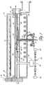
- FIGURE 1 shows a vapor deposition reactor 10, including a quartz process or reaction chamber 12, constructed in accordance with a preferred embodiment, and for which the methods disclosed herein have particular utility. While originally designed to optimize epitaxial chemical vapor deposition (CVD) of silicon on a single substrate at a time, the inventors have found the superior processing control to have utility in a number of different types of vapor deposition. For example, the ALD processes described hereinbelow can be conducted in the illustrated CVD reactor of FIGURE 1, preferably with adjustments to the inlet flange to avoid intermixing separate reactant pulses prior to entry in the reaction chamber. Moreover, the illustrated reactor 10 can safely and cleanly accomplish multiple treatment steps sequentially in the same chamber 12.
- CVD epitaxial chemical vapor deposition
- the basic configuration of the reactor 10 is available commercially under the trade name EpsilonTM from ASM America, Inc. of Phoenix, AZ. It will be understood, however, that the processes described herein are applicable and have utility in a number of different reactor configurations.
- EpsilonTM reactor of FIGURE 1 is employed for plasma enhanced or assisted CVD of dielectric materials, in accordance with processes described below.
- the chamber of FIGURE 1 can also be employed for CVD of electrode materials in a cluster tool along with an ALD module (see FIGURES 2A to 2C) for ALD of dielectric materials in accordance with processes described below.
- a plurality of radiant heat sources are supported outside the chamber 12 to provide heat energy in the chamber 12 without appreciable absorption by the quartz chamber 12 walls. While the preferred embodiments are described in the context of a "cold wall" reactor for processing semiconductor wafers, it will be understood that the processing methods described herein will have utility in conjunction with other heating/cooling systems, such as those employing inductive or resistive heating.
- the illustrated radiant heat sources comprise an upper heating assembly of elongated tube-type radiant heating elements 13.
- the upper heating elements 13 are preferably disposed in spaced-apart parallel relationship and also substantially parallel with the reactant gas flow path through the underlying reaction chamber 12.
- a lower heating assembly comprises similar elongated tube-type radiant heating elements 14 below the reaction chamber 12, preferably oriented transverse to the upper heating elements 13. Desirably, a portion of the radiant heat is diffusely reflected into the chamber 12 by rough specular reflector plates (not shown) above and below the upper and lower lamps 13,14, respectively.
- a plurality of spot lamps 15 supply concentrated heat to the underside of the substrate support structure (described below), to counteract a heat sink effect created by cold support structures extending through the bottom of the reaction chamber 12.
- Each of the elongated tube type heating elements 13, 14 is preferably a high intensity tungsten filament lamp having a transparent quartz envelope containing a halogen gas, such as iodine. Such lamps produce full-spectrum radiant heat energy transmitted through the walls of the reaction chamber 12 without appreciable absorption. As is known in the art of semiconductor processing equipment, the power of the various lamps 13, 14,15 can be controlled independently or in grouped zones in response to temperature sensors.
- a substrate preferably comprising a silicon wafer 16 is shown supported within the reaction chamber 12 upon a substrate support structure 18.
- substrate broadly refers to any surface on which a layer is to be deposited.
- the principles and advantages described herein apply equally well to depositing layers over numerous other types of substrates, including, without limitation, glass substrates such as those employed in flat panel displays.
- the illustrated support structure 18 includes a substrate holder or susceptor 20, upon which the wafer 16 rests, and a support spider 22.
- the spider 22 is mounted to a rotating shaft 24, which extends downwardly through a tube 26 depending from the chamber lower wall.
- the tube 26 communicates with a source of purge or sweep gas which can flow during processing, inhibiting process gases from escaping to the lower section of the chamber 12.
- a plurality of temperature sensors are positioned in proximity to the wafer 16.
- the temperature sensors may take any of a variety of forms, such as optical pyrometers or thermocouples.
- the number and positions of the temperature sensors are selected to promote temperature uniformity, as will be understood in light of the description below of the preferred temperature controller.
- the temperature sensors directly or indirectly sense the temperature of positions in proximity to the wafer.
- the temperature sensors comprise thermocouples, including a first or central thermocouple 28, suspended below the wafer holder 20 in any suitable fashion.
- the illustrated central thermocouple 28 passes through the spider 22 in proximity to the wafer holder 20.
- the reactor 10 further includes a plurality of secondary or peripheral thermocouples, also in proximity to the wafer 16, including a leading edge or front thermocouple 29, a trailing edge or rear thermocouple 30, and a side thermocouple (not shown).
- Each of the peripheral thermocouples are housed within a slip ring 32, which surrounds the substrate holder 20 and the wafer 16.
- Each of the central and peripheral thermocouples are connected to a temperature controller, which sets the power of the various heating elements 13, 14, 15 in response to the readings of the thermocouples.
- the slip ring 32 can be suspended by any suitable means.
- the illustrated slip ring 32 rests upon elbows 34 that depend from a front.chamber divider 36 and a rear chamber divider 38.
- the dividers 36, 38 desirably are formed of quartz. In some arrangements, the rear divider 38 can be omitted.
- the illustrated reaction chamber 12 includes an inlet port 40 for the injection of reactant and carrier gases, and the wafer 16 can also be received therethrough.
- An outlet port 42 is on the opposite side of the chamber 12, with the wafer support structure 18 positioned between the inlet 40 and the outlet 42.
- An inlet component 50 is fitted to the reaction chamber 12, adapted to surround the inlet port 40, and includes a horizontally elongated slot 52 through which the wafer 16 can be inserted.
- a generally vertical inlet 54 receives gases from remote sources, as will be described more fully below, and communicates such gases with the slot 52 and the inlet port 40.
- the inlet 54 can be modified from the original Epsilon® design for CVD and instead be configured to keep the gas flow from different ALD precursor sources separate until entry into the chamber 12, in order to avoid CVD-like reactions.
- An outlet component 56 also mounts to the process chamber 12 such that an exhaust opening 58 aligns with the outlet port 42 and leads to exhaust conduits 59.
- the conduits 59 can communicate with suitable vacuum means (not shown) for drawing process gases through the chamber 12.
- a pump or fan is preferably included to aid in drawing process gases through the chamber 12, and to evacuate the chamber for low pressure processing.
- the illustrated reactor 10 also includes a source 60 of excited species, preferably positioned upstream from the chamber 10.
- the excited species source 60 of the illustrated embodiment comprises a remote plasma generator, including a magnetron power generator and an applicator along a gas line 62.
- An exemplary remote plasma generator is available commercially under the trade name TRW-850 from Rapid Reactive Radicals Technology (R3T) GmbH of Kunststoff, Germany.
- microwave energy from a magnetron is coupled to a flowing gas in an applicator along a gas line 62.
- a source of precursor gases 63 is coupled to the gas line 62 for introduction into the excited species generator 60.
- a source of carrier gas 64 is also coupled to the gas line 62.
- One or more further branch lines 65 can also be provided for additional reactants.
- the gas sources 63, 64 can comprise gas tanks, bubblers, etc., depending upon the form and volatility of the reactant species.
- Each gas line can be provided with a separate mass flow controller (MFC) and valves, as shown, to allow selection of relative amounts of carrier and reactant species introduced to the excited species generator 60 and thence into the reaction chamber 12.
- MFC mass flow controller
- the excited species can be generated within or immediately adjacent the process chamber (see FIGURES 2A to 2C and corresponding text).
- Wafers are preferably passed from a handling chamber (not shown), which is isolated from the surrounding environment, through the slot 52 by a pick-up device.
- the handling chamber and the processing chamber 12 are preferably separated by a gate valve (not shown) of the type disclosed in U.S. Patent No. 4,828,224.
- the total volume capacity of a single-wafer process chamber 12 designed for processing 200 mm wafers is preferably less than about 30 liters, more preferably less than about 20 liters, and most preferably less than about 10.
- the illustrated chamber 12 has a capacity of about 7.5 liters. Because the illustrated chamber 12 is divided by the dividers 36, 38, wafer holder 20, ring 32, and the purge gas flowing from the tube 26, however, the effective volume through which process gases flow is around half the total volume (about 3.77 liters in the illustrated embodiment). Of course, it will be understood that the volume of the single-wafer process chamber 12 can be different, depending upon the size of the wafers for which the chamber 12 is designed to accommodate.
- a single-wafer processing chamber 12 of the illustrated type preferably has a capacity of less than about 100 liters, more preferably less than about 60 liters, and most preferably less than about 30 liters.
- One 300 mm wafer processing chamber has a total volume of about 24 liters, with an effective processing gas capacity of about 11.83 liters.
- a plurality of vapor-phase precursor sources are connected to the inlet 54 via gas lines with attendant safety and control valves, as well as mass flow controllers ("MFCs"), which are coordinated at a gas panel.
- the gas sources can include, for example, a source of carrier gas (e.g. , H 2 or N 2 ); metal precursors (e.g ., ZrCl 4 , HfCl 4 , WF 6 , TiCl 4 , CuCl, etc.); an oxidant source gas (e.g. , O 2 , O 3 , O radicals, H 2 O, NO, N 2 O, etc.); a nitrogen source gas (e.g.
- vapor-phase sources can include liquid reactant sources in a bubbler, and a gas line for bubbling and carrying vapor phase reactants from the bubbler to the reaction chamber 12.
- Process gases are communicated to the inlet 54 in accordance with directions programmed into a central controller (including a memory and a microprocessor) and distributed into the process chamber 12 through injectors. After passing through the process chamber 12, unreacted process gases and gaseous reaction by-products are exhausted to a scrubber to condense environmentally dangerous fumes before exhausting to the atmosphere.
- a central controller including a memory and a microprocessor
- FIGURE 2A illustrates one embodiment of an ALD or ALE reactor 130 having certain features and advantages according to the present invention.
- the illustrated embodiment includes a reaction chamber 132, which defines a reaction zone.
- a wafer or substrate 136 is disposed within the reaction chamber 132 and is supported by a pedestal 138, which preferably is configured to open the chamber 132 and move the substrate 136 in and out of the reaction chamber 132.
- the reactor 130 can include a wafer inlet/outlet port and an external robot with a robot arm.
- two precursors are supplied to the reaction chamber 132.
- the first precursor is supplied to the reaction chamber 132 through a first precursor conduit 140.
- the second precursor is supplied to the reaction chamber 132 through a second precursor supply conduit 142.
- Each supply conduit is connected to a precursor supply source (not shown) and preferably a purge gas source (not shown).
- the purge gas is an inert gas and can be, by way of example, nitrogen or argon.
- the purge gas can also be used as a carrier gas to transport the first and/or second precursors.
- the reactor 130 also includes an exhaust 144 for removing material from the reactor chamber 132.
- a showerhead plate 146 is positioned within the reaction chamber 132.
- the showerhead plate 146 is a single integral element
- the showerhead plate 146 preferably spans across the entire reaction zone and divides the reaction chamber 132 into an upper chamber 148, defining a plasma cavity 149, and a lower chamber 150.
- the showerhead plate 146 defines, at least in part, a plurality of passages 152 that connect the upper chamber 148 to the lower chamber 150.
- such passages 152 are formed by providing small holes in the showerhead plate 146 that are located generally above the substrate 136. In this manner, the showerhead plate 146 substantially prevents the second precursor from entering the lower chamber 150 until the flow from the second conduit 142 is generally above the substrate 136.
- the upper chamber 148 of the illustrated reaction chamber 132 defines the separate plasma cavity 149 for creating in-situ radicals.
- in-situ radicals can be used to facilitate reactions on the surface of the substrate.
- a plasma can be created within the plasma cavity 149 in a variety of ways, such as, for example, using a capacitor electrode positioned inside or outside the plasma cavity (i.e., a capacitively coupled plasma), a RF coil ( i.e ., a inductively coupled plasma), light, ionizing radiation, heat (e.g ., heated tungsten filament can be used to form hydrogen radicals from hydrogen molecules), and/or chemical reactions to generate the plasma.
- a capacitor electrode positioned inside or outside the plasma cavity (i.e., a capacitively coupled plasma), a RF coil ( i.e ., a inductively coupled plasma), light, ionizing radiation, heat (e.g ., heated tungsten filament can be used to form hydrogen radicals from hydrogen molecules), and/or
- a capacitor electrode 154 is positioned outside the reaction chamber 132 and the plasma cavity 149.
- the showerhead plate 146 is positioned between the plasma cavity 149 and the substrate 136 and, in the illustrated embodiment, is also used as the other electrode.
- This embodiment has several advantages. For example, even if the radicals are very short-lived, the path to the growth surface (i.e ., the substrate 136) is short enough to guarantee their contribution to the growth reaction. Also the upper chamber 148 can be made large enough to provide necessary space for plasma ignition and also to separate the plasma from the growth surface thus protecting it from the damaging effects of the energetic particles and charges in the plasma.
- FIGURE 2B illustrates a modified embodiment of a reactor 160 that also utilizes plasma cavity 162.
- the reactor 160 includes a reaction chamber 163, which defines a reaction space 164.
- a substrate 166 is positioned within the reaction space and is supported by a wafer holder 170, which can be heated.
- a first precursor is introduced into the reaction space via a first supply conduit 172.
- the first supply conduit 172 and the reaction chamber 163 are arranged such that the flow of the first precursor within the reaction chamber is generally parallel to a reaction surface of the substrate 166.
- An exhaust 174 and a pump are preferably provided for removing material from the reaction chamber 163.
- the reactor 160 also includes an upper chamber 175 defining the plasma cavity 162, which, in the illustrated embodiment, is located generally above the reaction space 164.
- the upper chamber 175 defines the plasma cavity 162 in which the in-situ radicals are generated.
- a second precursor is introduced into the plasma cavity 162 via a second supply conduit 176. Radicals and other excited species are generated from the plasma that is generated in the upper chamber 175.
- the illustrated embodiment utilizes a planar RF TCP coil and RF shield 177, which are separated from the plasma cavity 162 by a window 178 made of, for example, quartz.
- a planar induction coil is described in the Journal of Applied Physics, Volume 88, Number 7, 3889 (2000) and the Journal of Vacuum Science Technology, A 19(3), 718 (2001).
- the plasma cavity 162 and the reaction space 164 are separated by a radical or showerhead plate 180.
- the showerhead plate 180 preferably defines a plurality passages 182 through which radicals formed in the plasma cavity can flow into the reaction space 164.
- the flow through the passages 182 is generally directed towards the reaction surface of the substrate 166.
- the space between the showerhead plate 180 and the substrate 166 can be as small as a few millimeters. Such an arrangement provides ample radical concentration at the wafer surface, even for short-lived radicals.
- purge gases can be continuously supplied to the plasma cavity 162 through a purge inlet 184.
- the upper chamber 175 can operate at a substantially constant pressure regime.
- the showerhead plate 180 and surrounding components adjacent to the reaction chamber 163 may be heated, either as a result of the plasma on one side on the showerhead plate 180 and/or a heated wafer holder 170 on the other side, or by separately heating the showerhead plate 180.
- the RF power can be used to alternately switch the radical concentration in the flow.
- the supply of precursors to the plasma cavity can be alternately switched.
- FIGURE 2C illustrates another modified embodiment of an ALD or ALE reactor 190 that also utilizes a plasma cavity.
- the plasma in the plasma cavity 162 is capacitively coupled.
- the illustrated embodiment includes a capacitor electrode 192, which is disposed in the plasma cavity 162 above the showerhead plate 180. This arrangement is similar to the arrangement shown in FIGURE 2A, except that the electrode is positioned inside the reaction chamber 163.
- a general process sequence for forming a transistor gate stack on a semiconductor substrate is shown.
- a substrate is first cleaned 70 and then a gate dielectric is deposited 72.
- the gate dielectric desirably comprises a high k material with high nitrogen content at both upper and lower interfaces and low nitrogen content in the bulk therebetween.
- a gate electrode is deposited 74, the gate is patterned and etched 76 (such as by conventional photolithographic processes).
- the substrate is subjected to source/drain reoxidabon after patterning, prior to continuing processing 78 to complete the integrated circuit
- a semiconductor substrate 100 is provided on or in a workpiece.
- the semiconductor substrate 100 typically comprises an epitaxial silicon layer or the upper surface of a single-crystal, intrinsically doped silicon wafer, although the skilled artisan will appreciate that other semiconductor materials (e.g . III-V materials) can be substituted.
- the substrate Prior to the illustrated process, the substrate is first cleaned to remove contaminants and naturally occurring or native oxide on the semiconductor structure.
- wafer cleaning prior to gate oxide growth is conducted ex situ prior to loading the wafer into the process chamber.
- wafers may be cleaned in an SCl/HF wet etch bath.
- an integrated HF and acetic acid vapor clean can be conducted in a neighboring module within a cluster tool, reducing transport time and opportunity for recontamination or reoxidation.
- the cleaning oxide left by the SCI step is not removed, but is instead used as the initial oxide layer.
- a hydrogen bake step can be conducted within the chamber to sublimate native oxide. Small amounts of HCl vapor can be added to this step to aid in cleaning metal contaminants and the like during the hydrogen bake.
- plasma products can assist or conduct in situ cleaning, such as by substituting H radicals for hydrogen gas.
- the wafer or other substrate is loaded into the process chamber.
- Cleaning of native oxide tends to leave a hydrogen-terminated surface, which advantageously inhibits spontaneous reoxidation upon exposure to the clean room environment or other source of oxidants. Such hydrogen termination may need to be desorbed prior to further processes.
- a high k dielectric layer 110 is formed over the substrate 100. Preferred methods of forming the high k dielectric layer 110 are described in more detail below.
- a seed or wetting layer 115 is optionally deposited directly over the cleaned surface of the gate dielectric 110, followed by a bulk silicon-containing layer 120 over the silicon-containing seed layer 115.
- the deposition preferably takes place within the preferred single wafer CVD reactor of FIGURE 1, available under the trade name EpsilonTM from ASM America of Phoenix, AZ. If employed, the wetting layer 115 is generally indistinguishable from the overlying bulk layer 120, and so is typically not apparent in the final structure (FIGURE 8).
- the gate electrode 115, 120 preferably contains silicon and is CVD deposited.
- the gate electrode can comprise a CVD polysilicon, doped or undoped, or a silicon germanium alloy, preferably having the form Si 1-x Ge x .
- Gate electrode formation typically comprises two stages, as illustrated in FIGURES 6-7: a seed phase and a bulk phase.
- the silicon seed or wetting layer 115 serves to improve nucleation relative to direct deposition of SiGe. If included, conditions are arranged in the seed phase to minimize chemical reduction of the underlying high k.
- the illustrated high k material comprises HfO 2 or ZrO 2 , which has been found particularly susceptible to reduction during conventional polysilicon or poly-SiGe deposition.
- a low reduction seed layer deposition is described in U.S. provisional patent application No. 60/279,256, filed March 27, 2001, entitled INTEGRATION OF HIGH K GATE DIELECTRIC.
- Conditions can then be arranged in the bulk phase to increase the deposition rate, relative to that of the previous step.
- the preferred high k dielectric 110 includes a relatively high nitrogen content at the upper interface. Accordingly, reduction of the high k dielectric may be sufficiently attenuated to avoid special low-reduction seed processing. Further, high nitrogen content at the upper interface can also improve subsequent nucleation of the gate electrode (e.g., Si, SiGe and particularly in situ doped Si and SiGe). Accordingly, the seed phase can be omitted.
- the gate electrode e.g., Si, SiGe and particularly in situ doped Si and SiGe.
- gate stacks typically are insulated by blanket deposition of a dielectric and spacer etch. Transistor active areas are then doped to form source and drain regions on either side of the patterned electrodes, and wiring or "back end" processes complete the circuit.
- FIGURE 8 illustrates a transistor gate formed after patterning and etching the layers described above.
- a semiconductor substrate 200 is shown with a transistor gate stack 210 formed thereover.
- the substrate 200 comprises an upper portion of a single-crystal silicon wafer, though the skilled artisan will appreciate that the substrate can also comprise other semiconductor materials.
- the gate stack 210 includes a polysilicon or poly-SiGe gate electrode layer 220. Sidewall spacers 230 and an insulating layer 240 protect and isolate the electrode 220 in a conventional manner. Also illustrated is a more highly conductive strapping layer 250, typically including metal, over the silicon-containing gate electrode layer 220. The strap 250 facilitates rapid signal propagation among transistor gates across the wafer, connecting the gates to logic circuits.
- a gate dielectric 260 formed by the exemplary processes described below, separates the gate electrode 220 from the substrate 200. As noted in the Background section above, the gate dielectric 260 is a critical feature in the pursuit of denser and faster circuits.
- integrated circuit transistors can have a variety of forms that do not all resemble that of FIGURE 8.
- the graded dielectric layer of the preferred embodiments will have application to gate dielectric layers in a variety of transistor types (e.g., heterojunction BiCMOS transistors), as well as to a variety of other ultrathin dielectric layers having other functions within an integrated circuit (e.g., capacitor dielectric, tunneling dielectric, etc.).
- high k materials are generally forms of metallic oxide with k values greater than about 7, including aluminum oxide (Al 2 O 3 ), zirconium oxide (ZrO 2 ), hafnium oxide (HfO 2 ), tantalum oxide (Ta 2 O 5 ), barium strontium titanate (BST), strontium bismuth tantalate (SBT), and lanthanide oxides.
- the last listed dielectrics include oxides of such physically stable "rare earth” elements as scandium (Sc), yttrium (Y), lanthanum (La), cerium Ce, praseodymium (Pr), neodymium (Nd), samarium (Sm), europium (Eu), gadolinium (Gd), terbium (Tb), dysprosium (Dy), holmium (Ho), erbium (Er), thulium (Tm), ytterbium (Yb) and lutetium (Lu).
- the high k material of the preferred embodiments can comprise any of the above-mentioned materials.
- high k materials incorporated into the dielectric layer of the illustrated embodiments comprise oxides of Group 4 metals, particularly zirconium oxide (ZrO 2 ) hafnium oxide (HfO 2 ), and have a dielectric constant greater than about 10.
- the preferred high k dielectric layer incorporates high k material throughout the thickness of the layer, and furthermore incorporate a controlled amount and distribution of an impurity, particularly nitrogen.
- this impurity is incorporated to a greater extent at upper and lower interfaces of the dielectric material, and is incorporated during the deposition process.
- two separate nitrogen peaks are provided through the thickness of the dielectric.
- FIGURE 9 illustrates a theoretical Auger profile showing nitrogen content through the thickness of the preferred high k dielectric.
- the left side of the graph represents the upper or top interface between the dielectric and the overlying gate electrode, showing an impurity concentration peak of X.
- the right side of the graph represents the lower or bottom interface between the dielectric and the semiconductor substrate surface, showing an impurity concentration peak of Y.
- a bulk portion of the layer between the two separate impurity concentration peaks has a minimum impurity concentration level generally indicated by Z.
- the dielectric upper interface includes between about 1% and 10% atomic ratio of nitrogen and is preferably between about 5 ⁇ and 20 ⁇ in thickness, more preferably between about 5 ⁇ and 10 ⁇ .
- this top interface serves to protect the bulk of the high k material from diffusion of impurities (e.g ., electrical dopants such as boron) from the overlying gate electrode and to inhibit silicidation reactions between the overlying gate electrode and the high k material, thereby maintaining thermal stability of the high k material, particularly during subsequent source/drain reoxidation.
- impurities e.g ., electrical dopants such as boron
- nitrogen content at the upper interface desirably facilitates nucleation during deposition of the overlying gate electrode, particularly SiGe, while resisting diffusion of reducing agents (e.g. , hydrogen) during such deposition.
- Reducing agents can disadvantageously convert the high k dielectric to metallic conductors and cause electrical leakage paths through the dielectric.
- the bulk of the dielectric preferably includes less than about 0.1% (atomic ratio) nitrogen, more preferably less than about 0.01% nitrogen, and for the illustrated gate dielectric function is between about 20 ⁇ and 30 ⁇ in thickness.
- low nitrogen content in the bulk of the illustrated high k material improves overall film quality.
- Substantially pure metal oxide (e.g., ZrO 2 or HfO 2 ) in the bulk avoids undercoordinated dangling bonds, which can otherwise form charge trap sites.
- the lower interface preferably includes greater than about 0.1% (atomic ratio) nitrogen, more preferably between about 0.1% and 1% nitrogen.
- the lower interface with this content has a thickness between about 5 ⁇ and 10 ⁇ , more preferably closer to about 5 ⁇ .
- the nitrogen content at this lower interface advantageously improves interface reliability at the substrate and inhibits oxidation of the substrate during high k deposition and subsequent processing. Such oxidation can disadvantageously lower the effective permittivity (k value) of the gate dielectric.
- the nitrogen level is lower than that of the upper interface, however, to reduce the advent of interface trap sites that might be induced by nitrogen at the substrate interface.
- the nitrogen content in the upper interface is more than about 5 times the nitrogen content in the lower interface, more preferably about one order of magnitude greater.
- the nitrogen-containing high k layers preferably have a thickness between about 20 ⁇ and 60 ⁇ .
- the described high k dielectric will also have other applications in integrated circuits.
- a thicker high k layer can be employed, such as 150 ⁇ to 200 ⁇ in thickness, having ultrathin nitrogen-containing interfaces.
- an upper nitrogen-containing interface as described above, can stabilize the high k material during subsequent processing.
- a lower nitrogen-containing interface can be omitted for a DRAM capacitor dielectric.
- the high k material as described above, can be deposited by any suitable process, including PVD, CVD, MOCVD, ALD, etc.
- nitrogen incorporation is desirably achieved in a controlled fashion during deposition.
- silicon oxide gate dielectric films are made by thermal oxidation of the underlying silicon substrate.
- nitrogen-containing gases can be added to the main oxygen stream, and/or a post-deposition treatment can be performed with nitrogen-containing gases or nitrogen implantation.
- Such methods can either incorporate nitrogen into the oxide material to form silicon oxynitride (SiO x N y ) or form a Si 3 N 4 layer over the oxide.
- oxide, whether deposited or thermally grown, are later treated for nitrogen incorporation by diffusion.
- nitrogen incorporation is varied during conventional thermal CVD, performed at relatively high temperatures, and interdiffusion inevitably takes place.
- CVD with variable nitrogen incorporation through remotely generated nitrogen radicals
- ALD with variable nitrogen incorporation through varying the constituents of the plural cycles.
- ALD can optionally also employ nitrogen radicals in the controlled fashion described with respect to the CVD embodiment.
- both embodiments benefit from low temperature deposition, which helps to maintain the desired nitrogen profile.
- deposition temperatures are below about 500°C and more preferably below about 400°C.
- a high k material is deposited with varying nitrogen content throughout the deposition process during chemical vapor deposition (CVD).
- Nitrogen is supplied by way of a remote plasma source 60, such as that described with respect to FIGURE 1.
- the amount of nitrogen incorporated into the layer, as it is deposited, is varied at least in part by varying the supply of nitrogen radicals generated by the remote source.
- high k metal oxide is deposited by a form of CVD employing metal-organic precursors (MOCVD).
- MOCVD metal-organic precursors
- organic metal source gases tend to decompose at relatively low temperatures.
- a vapor phase, organic source of hafnium or zirconium is simultaneously provided with a vapor phase source of oxygen.
- Nitrogen is provided in the form of nitrogen radicals from a remote plasma source, advantageously also enabling low temperature reactions.
- the ratio of nitrogen radicals or excited species to oxygen is varied during the process to be higher at initial stages (representing the lower interface), low to zero during intermediate stages (representing the dielectric bulk) and higher again at the terminal stages (representing the upper interface).
- the nitrogen content in the deposited high k material is thereby varied in a controlled fashion, allowing for two separate nitrogen peaks ( see, e.g., FIGURE 9).
- the relative amount of nitrogen can be varied in a variety of manners.
- the flow of nitrogen source gas e.g., ammonia, diatomic nitrogen or hydrazine
- the flow of nitrogen source gas is varied, such that it is highest during terminal stages of the deposition, at an intermediate level during initial stages of the deposition, and lowest ( e.g. , zero) during intermediate stages of the deposition.
- the flow of carrier gas through the remote plasma generator is varied.
- the skilled artisan will appreciate that such variation will have a non-linear effect upon the amount of nitrogen radicals generated.
- High carrier flow can support denser plasma generation and thus greater nitrogen radical concentration up to a point, but dilution due to greater overall gas flow during the CVD process can reduce nitrogen incorporation into the deposited film.
- both oxygen source and nitrogen source gases are provided through the remote plasma generator.
- the relative rates of dissociation can be changed, thereby changing the relative generation of N radicals as compared to O radicals. For example, using N 2 as the nitrogen source and O 2 as the oxygen source, increasing power will increase dissociation of both sources up to a point As power is increased further, the rate of O 2 dissociation will level off while the rate of N 2 dissociation continues to increase with increasing power.
- altering power applied to the remote plasma generator will vary the amount of nitrogen excited species supplied to the CVD process in a straight forward manner.
- microwave power applied to a remote plasma processor can be varied between about 800 W and 2 kW.
- the high k material is deposited by an atomic layer deposition (ALD) process.
- ALD is a chemically self-limiting process, whereby alternated pulses of reaction precursors saturate a substrate and leave no more than one monolayer of material per pulse.
- the precursors are selected to ensure self-saturating reactions, because at least one pulse per cycle leaves a chemisorbed species with a surface termination that is non-reactive with the gas phase reactants of the same pulse.
- Such a termination is left by "tails" or ligands of the source chemical, such as organic tails or halide tails.
- a subsequent pulse of different reactants do react with the tails left on the chemisorbed layer of a previous pulse to enable continued deposition.
- each cycle of alternated pulses leaves no more than about one molecular layer of the desired material.
- ALD type processes have been presented by T. Suntola, e.g. in the Handbook of Crystal Growth 3, Thin Films and Epitaxy, Part B: Growth Mechanisms and Dynamics, Chapter 14, Atomic Layer Epitaxy, pp. 601-663, Elsevier Science B.V. 1994.
- the deposition is conducted in a PulsarTM 2000 reactor (commercially available from ASM Microchemistry of Espoo, Finland), which is designed for ALD processes.
- the ALD tools of FIGURES 2A-2C can be employed with or without application of plasma power to the upper chamber.
- ALD facilitates the formation of thin films monolayer by monolayer. Indeed, control exists on a smaller than monolayer scale, due to steric hindrance of bulky source chemical molecules producing less than one monolayer per cycle.
- the capability of layering atomically thin monolayers enables forming more precise concentration gradients from the lower surface (e.g., gate dielectric/Si substrate interface) to the upper surface (e.g., gate electrode/gate dielectric interface).
- each discrete monolayer can be tailored by selectively introducing the desired chemistry for each monolayer to be deposited.
- ALD atomic layer deposition
- a particular combination of introduced gases react with, deposit or adsorb upon the workpiece until, by the nature of the deposition chemistry itself, the process self-terminates. Regardless of the length of exposure, the process gases do not contribute further to the deposition.
- different chemical combinations are introduced in the process chamber such as will react with or adsorb upon the previously formed monolayer.
- the second chemistry or a subsequent chemistry forms another monolayer, also in a self-limiting manner. These self-limiting monolayers are alternated as many times as desired to form a film of suitable thickness.
- a thin film of 60 ⁇ zirconium oxide is formed by an ALD process alternating ZrCl 4 and H 2 O described below in about 100 cycles.
- the composition can be changed such that a different impurity concentration can be incorporated into the first monolayer as compared to that incorporated into the last monolayer.
- ALD of silicon oxide dielectric layers, with a graded nitrogen content is disclosed in U.S. Patent Application No. 09/800,757, filed March 6, 2001, entitled GRADED THIN FILMS.
- the preferred embodiment modifies ALD deposition of a high k metal oxide by selectively incorporating nitrogen during selected stages of the deposition.
- a metal source gas suitable for chemisorption of a self-limited partial or full monolayer per pulse, is alternated with an oxidant pulse.
- exemplary oxidant source gases include oxygen, water, hydrogen peroxide, ozone, alcohols (e.g., methanol, ethanol, isopropanol), etc.
- the process can include additional pulses, such as additional metal source pulses for more complex metal oxides, and gettering pulses for stripping ligands between pulses.
- a basic ALD process for deposition of ZrCl 4 is first described prior to describing two modifications employed for incorporating nitrogen, described below with respect to FIGURES 10 and 11.
- the reaction space is evacuated to vacuum with a mechanical vacuum pump. After evacuation the pressure of the reaction space was adjusted to about 5-10 mbar (absolute) with flowing nitrogen gas that had a purity of 99.9999%. Then the reaction space is stabilized at 300°C.
- a ZrCl 4 source is kept between about 180°C and 210°C, more preferably about 200.
- Each cycle of the ALD process comprises a plurality of pulses.
- ZrCl 4 vapor is introduced to the reaction chamber and exposed the wafer surface for 0.1 s. This is referred to as pulse A or the "metal pulse.”
- the reaction chamber is purged with nitrogen gas for 1.0 s to remove surplus ZrCl 4 and byproducts from the reaction chamber. This is referred to as purge A.
- water vapor is introduced to the reaction chamber and exposed to the wafer surface for 0.3 s. This is referred to as pulse B or the "oxidant pulse.” Residual H 2 O and reaction byproducts were removed by purging the reaction chamber for 3.0 s. This is referred to as purge B.
- the reactants are supplied in sufficient quantity for the given other parameters to saturate the surface.
- the average deposition rate using the foregoing chemicals is about 0.59 ⁇ /cycle at 300°C, such that the ZrO 2 thickness was about 30 ⁇ . Similar process conditions using HrCl 4 in place of ZrCl 4 will produce HfO 2 .
- temperatures during the process preferably fall between about 250°C and 500°C, more preferably between about 300°C and 350°C, depending upon the acceptable levels of chlorine in the film.
- the temperature is more preferably at the low end of this range, between about 200°C and 250°C, and most preferably at about 225°C.
- the temperature is more preferably at the high end of this range, between about 250°C and 500°C, and most preferably between about 300°C and 350°C.
- mixtures of amorphous and crystalline composition result at the boundary of these two regimes.
- the illustrated process utilizes temperatures between about 300°C and 350°C, producing a largely crystalline ZrO 2 or HfO 2 film. More generally, the metal pulse A preferably is conducted for between about 0.05 s and 1.0 s, purge A for between about 0.5 s and 10.0 s, oxidation pulse B for between about 0.05 s and 0.5 s and purge B for between about 0.5 s and 10.0 s.
- the pulse times in particular and all parameters in general can be varied within relatively large windows within which ALD reactions can occur.
- One of the stricter limitations for accomplishing truly self-limited reactions in ALD is that the temperature is preferably kept above the temperatures at which the source chemicals condense, but below the temperatures at which the source chemicals thermally decompose. Unlike CVD, however, deposition rates remain constant anywhere within this relatively large temperature window, such that strict temperature uniformity across a substrate is not required in order to accomplish conformal deposition.
- the metal monolayer formed in the metal phase is self-terminated with chloride, which does not readily react with excess ZrCl 4 under the preferred conditions.
- the preferred oxygen source gas reacts with or adsorbs upon the chloride-terminated surface during the oxygen phase in a ligand-exchange reaction limited by the supply of zirconium chloride complexes previously adsorbed. Moreover, oxidation leaves a hydroxyl and oxygen bridge termination that does not further react with excess oxidant in the saturative phase.
- sufficient cycles are conducted to grow between about 20 ⁇ and 60 ⁇ of ZrO 2 . More preferably, sufficient cycles are conducted to grow between about 20 ⁇ and 40 ⁇ .
- the dielectric constant of pure zirconium oxide can range between about 18 and 24.
- an impurity source gas is also provided to at least one of the cycles in the alternating process, selected to improve the functional qualities of the dielectric.
- the impurity preferably comprises nitrogen, and the impurity source gas preferably comprises ammonia (NH 3 ) or hydrazine (N 2 H 4 ) added to the alternating process. Both ammonia and hydrazine are fairly reactive gases, making them suitable for low temperature ALD processing.
- a first arrangement nitrogen is incorporated during the oxidant pulses of selected cycles.
- a second arrangement nitrogen is incorporated during selected cycles in its own separate pulses.
- different amounts of nitrogen can be incorporated at different points in the deposition process, allowing for a high degree of control over nitrogen coment even through the thickness of extremely thin layers, while low deposition temperatures minimize interdiffusion and ensure maintenance of the desired nitrogen profile.
- the first arrangement involves alternating adsorption of no more than about a monolayer of metal with oxidation of the previously adsorbed monolayer in an ALD metal oxide process.
- nitrogen can also be selectively incorporated.
- oxynitride films with any desired ratio of oxygen to nitrogen can be grown.
- reactant ratios during the cyclical process the composition formed by each cycle can be tailored.
- the deposition begins with metal oxynitride deposition, transitions to substantially pure metal oxide and ends with metal oxynitride.
- a highly reactive nitrogen source gas such as ammonia or hydrazine
- NH 3 is added to different oxidant source gas pulses throughout the process.
- a desired amount of nitrogen can be selectively incorporated into each monolayer of metal oxide and a metal oxynitride layer results with a tailored nitrogen content profile.
- the reaction between ammonia and the adsorbed metal complex will have a different thermodynamic favorability, as compared to the reaction between the oxidant and the metal complex. Accordingly, the proportions of ammonia to oxidant do not necessarily equal the proportions of nitrogen to oxygen in the resultant metal oxynitride.
- the skilled artisan can readily account for thermodynamic competition through routine experimentation to determine the appropriate parameters for the desired levels of nitrogen incorporation. Providing nitrogen active species through a remote plasma generator, particularly in conjunction with oxygen active species, can maximize the effect of varying the ratio of oxygen to nitrogen sources in a thermodynamically competitive single-pulse reaction.
- FIGURE 10 is a gas flow diagram in accordance with one embodiment, illustrating four cycles 301a - 301d in an exemplary self-limiting deposition sequence.
- the four cycles might represent, for example, the last four cycles in forming the upper interface of the preferred high k dielectric.
- the illustrated sequence includes a constant flow of a carrier gas 300.
- a first pulse or spike 302a of the metal source gas is provided to form the first self-terminated metal complex monolayer.
- a first purge step 303 during which carrier gas continues to flow until the metal source gas has been removed from the chamber, a first oxidant source gas pulse or spike 304a is provided.
- a second metal source gas pulse 302b is provided, followed by a second oxidant source gas 304b, a third metal source gas pulse 302c, a third oxidant source gas pulse 304c, etc. in alternating pulses separated by purge steps 303.
- a first impurity source gas pulse 306b is provided, preferably during an oxidant source gas pulse 304b.
- a relatively low percentage of the impurity source gas (preferably comprising NH 3 ) is provided during this first pulse 306b.
- progressively greater flows of the impurity source gas are provided in pulses 306c, 306d, etc. Where progressively greater flows of the impurity source gas are employed, it can be advantageous to supply reactants perpendicularly to the substrate surface, such as by way of an overhead showerhead.
- all of the substrate surface is preferably exposed simultaneously to the gas mixture.
- the showerhead structures of FIGURES 2A-2C, configured for ALD by separation of precursor channels, are particularly advantageous for such simultaneous exposure, with or without activation of a plasma in the upper chamber. Thus, concentration gradients from an inlet side to the exhaust side of the substrate can be avoided.
- FIGURE 10 is schematic only, and not drawn to scale. Additionally, the preferred process conditions actually result in a full monolayer formed after a plurality of cycles. While theoretically the reactants will chemisorb at each available site on the exposed layer of the workpiece, physical size of the adsorbed species (and particularly with terminating ligands) will generally limit coverage with each cycle to a fraction of a monolayer. In the illustrated embodiment, on average roughly 0.59 ⁇ of ZrO 2 forms per cycle, such that a full monolayer effectively forms after several cycles, where each cycle is represented by a pair of metal source gas and oxidant source gas pulses.
- the oxidant source gas pulses 304a, 304b, etc. can also be reduced in the course of increasing the impurity source gas flow, depending upon the materials and the desired. Accordingly, nitrogen content in the resultant metal oxynitride dielectric layer can be increased from 0 percent in the bulk up to a maximum desired level (preferably between about 1% and 10% nitrogen by atomic ratio) at the upper interface.
- grading a nitrogen concentration in a simple metal oxide layer While the illustrated example comprises grading a nitrogen concentration in a simple metal oxide layer, skilled artisan will readily appreciate, in view of the disclosure herein, that the same principles can be applied to forming graded profiles in other gate dielectric materials, such as binary and ternary metal oxides (e.g ., BST, SBT) by ALD.
- additional gettering pulses can be provided to react with and volatilize harmful halides (e.g. , Cl) and halide compounds (e.g., ammonium halides, hydrogen halides).
- Such gettering pulses can comprises supplying strong reducing agents, such as triethyl boron (TEB), in pulses to the substrate during the ALD process, preferably during each cycle.
- TEB triethyl boron
- FIGURE 11 illustrates an arrangement in which nitrogen is added in separate nitrogen source gas pulses (e.g. , each comprising an ammonia pulse and a purge pulse) following oxidant phases.
- the nitrogen source gas pulse can replace or be used in addition to oxidant source gas pulses, such as one every ten cycles, during the terminal stages of deposition.
- the frequency of nitrogen source gas pulses e.g. , relative to the frequency of metal source pulses
- a high frequency of nitrogen source gas pulses can be employed initially, followed by a reduction of the nitrogen pulse frequency to achieve a substantially nitrogen-free bulk metal oxide.
- the basic alternating process depositing metal oxide (e.g. , by alternating metal and oxidant pulses) initially is modified to deposit a lower interface of a metal oxynitride with relatively low levels of nitrogen (e.g ., about 0.1% to 1% nitrogen by atomic ratio); continues with ALD of a substantially pure (e.g ., less than about 0.1% nitrogen) metal oxide in an intermediate portion of the process; and, by the time the desired dielectric thickness is reached, the alternating process again increases the frequency of nitrogen pulses to produce an upper interface of metal oxynitride with relatively higher levels of nitrogen (e.g ., about 1% to 10% nitrogen).
- ALD substantially pure metal oxide
- the process employs an intermediate reduction phase to remove halide tails, illustrated between metal and nitrogen source phases.
- This intermediate reduction phase avoids build up of hydrogen halides that could be harmful to exposed metal and reduces halide content in the dielectric. It will be understood, however, that in other arrangements the reduction phase can be performed in a different sequence or omitted.
- phase (1)-(4) are employed, with a relative small frequency of the nitrogen phase (4) to result in a low nitrogen content (e.g., 0.1% to 1% nitrogen by atomic ratio) at the substrate interface.
- phases (1)-(3) are employed in order to form substantially pure ZrO 2 in the bulk.
- phases (1)-(4) are again employed, with a relatively greater frequency of phase (4) to result in a higher nitrogen content (e.g., 1% to 10% nitrogen by atomic ratio) at the gate electrode interface.
- the reduction phase (2) is optional for all stages of deposition.
- the reduction phase enables gettering halides left by the metal halide source gases.
- the reduction phase is thus preferably employed to reduce the chlorine content in the growing film. Note that the reduction phase, if employed, need not be employed in every cycle and, if employed in every cycle, need not be employed immediately subsequent to the metal phase.
- FIGURE 11 illustrates and Table II above presents parameters for cycles of an ALD process for depositing of a graded layer of metal oxide and metal oxynitride.
- the layer serves as gate dielectric between a semiconductor substrate and a transistor gate electrode layer.
- a metal source gas comprises zirconium tetrachloride (ZrCl 4 );
- a carrier gas comprises nitrogen (N 2 );
- a reducing agent comprises Methyl boron (TEB);
- an oxidant source gas comprises water vapor (H 2 O) ; and
- a nitrogen source gas comprises ammonia (NH 3 ).
- Three-phase cycles 450 are shown in FIGURE 11. Such three-phase cycles 450 are conducted with highest frequency in forming the bulk of the dielectric, with lower frequency in forming the lower interface over the transistor channel, and with lowest frequency in forming the upper interface below the gate electrode.
- One four-phase cycle 455 is also shown.
- the four-phase cycle includes a nitrogen pulse and purge.
- Such four-phase cycles 455 are conducted with lowest frequency in forming the bulk of the dielectric, with higher frequency in forming the lower interface over the transistor channel, and with highest frequency in forming the upper interface below the gate electrode.
- the zirconium source gas pulse in a basic ZrO 2 ALD process can be periodically substituted by a trimethyl aluminum (TMA) pulse during initial deposition, forming an alumina-doped zirconium oxide lower interface.
- TMA trimethyl aluminum
- the TMA pulse can be provided with decreasing frequency until pure zirconium dioxide (ZrO 2 ) is formed for the bulk dielectric.
- ZrO 2 pure zirconium dioxide
- TMA serves as an aluminum source gas and can be deposited at the same temperature ( e.g. , 300°C) as the zirconium oxide ALD process.
- aluminum source gas can be introduced simultaneously and as an increasing proportion of the zirconium source gas during a metal pulse, which is continually alternating with an oxidant pulse.
- the skilled artisan can determine through routine experimentation what proportions of aluminum source gas to zirconium source gas should be used to obtain the desired material proportions in the layer.
- the skilled artisan will readily appreciate that other gate dielectric materials can also be created in this fashion.
- aluminum oxide serves as a good barrier diffusion with good electrical interface properties
- zirconium dioxide provides a higher overall dielectric constant value for the dielectric.
- the gate dielectric can again be graded from a high aluminum content lower interface to substantially pure ZrO 2 to a high aluminum content upper interface.
- the aluminum content at the interface provides an amorphous, good diffusion barrier that stabilizes the dielectric against reaction with upper or lower materials.
- the impurity can be supplied through a remote plasma generator.
- the supply of nitrogen excited species can be varied as described above with respect to the CVD embodiment.
- the reactors of FIGURES 2A-2C are particularly suited to supplying excited species to an ALD process, separately from other precursors.
Landscapes
- Engineering & Computer Science (AREA)
- Chemical & Material Sciences (AREA)
- Microelectronics & Electronic Packaging (AREA)
- Power Engineering (AREA)
- General Physics & Mathematics (AREA)
- Computer Hardware Design (AREA)
- Physics & Mathematics (AREA)
- Condensed Matter Physics & Semiconductors (AREA)
- Manufacturing & Machinery (AREA)
- Chemical Kinetics & Catalysis (AREA)
- General Chemical & Material Sciences (AREA)
- Crystallography & Structural Chemistry (AREA)
- Materials Engineering (AREA)
- Mechanical Engineering (AREA)
- Metallurgy (AREA)
- Organic Chemistry (AREA)
- Ceramic Engineering (AREA)
- Inorganic Chemistry (AREA)
- Chemical Vapour Deposition (AREA)
- Insulated Gate Type Field-Effect Transistor (AREA)
- Formation Of Insulating Films (AREA)
Applications Claiming Priority (5)
| Application Number | Priority Date | Filing Date | Title |
|---|---|---|---|
| US32683001P | 2001-10-02 | 2001-10-02 | |
| US326830P | 2001-10-02 | ||
| US10/260,370 US6960537B2 (en) | 2001-10-02 | 2002-09-26 | Incorporation of nitrogen into high k dielectric film |
| US260370 | 2002-09-26 | ||
| PCT/US2002/031072 WO2003030243A1 (en) | 2001-10-02 | 2002-09-27 | Incorporation of nitrogen into high k dielectric film |
Publications (2)
| Publication Number | Publication Date |
|---|---|
| EP1449240A1 EP1449240A1 (en) | 2004-08-25 |
| EP1449240B1 true EP1449240B1 (en) | 2006-05-31 |
Family
ID=26947948
Family Applications (1)
| Application Number | Title | Priority Date | Filing Date |
|---|---|---|---|
| EP02800389A Expired - Fee Related EP1449240B1 (en) | 2001-10-02 | 2002-09-27 | Incorporation of nitrogen into high k dielectric film |
Country Status (5)
| Country | Link |
|---|---|
| US (3) | US6960537B2 (ja) |
| EP (1) | EP1449240B1 (ja) |
| JP (1) | JP4566559B2 (ja) |
| DE (1) | DE60211940T2 (ja) |
| WO (1) | WO2003030243A1 (ja) |
Families Citing this family (564)
| Publication number | Priority date | Publication date | Assignee | Title |
|---|---|---|---|---|
| FI119941B (fi) * | 1999-10-15 | 2009-05-15 | Asm Int | Menetelmä nanolaminaattien valmistamiseksi |
| US6974766B1 (en) | 1998-10-01 | 2005-12-13 | Applied Materials, Inc. | In situ deposition of a low κ dielectric layer, barrier layer, etch stop, and anti-reflective coating for damascene application |
| US6727169B1 (en) * | 1999-10-15 | 2004-04-27 | Asm International, N.V. | Method of making conformal lining layers for damascene metallization |
| US6319766B1 (en) | 2000-02-22 | 2001-11-20 | Applied Materials, Inc. | Method of tantalum nitride deposition by tantalum oxide densification |
| US6620723B1 (en) | 2000-06-27 | 2003-09-16 | Applied Materials, Inc. | Formation of boride barrier layers using chemisorption techniques |
| US6551929B1 (en) | 2000-06-28 | 2003-04-22 | Applied Materials, Inc. | Bifurcated deposition process for depositing refractory metal layers employing atomic layer deposition and chemical vapor deposition techniques |
| US7964505B2 (en) | 2005-01-19 | 2011-06-21 | Applied Materials, Inc. | Atomic layer deposition of tungsten materials |
| US7405158B2 (en) | 2000-06-28 | 2008-07-29 | Applied Materials, Inc. | Methods for depositing tungsten layers employing atomic layer deposition techniques |
| US6936538B2 (en) | 2001-07-16 | 2005-08-30 | Applied Materials, Inc. | Method and apparatus for depositing tungsten after surface treatment to improve film characteristics |
| US7101795B1 (en) * | 2000-06-28 | 2006-09-05 | Applied Materials, Inc. | Method and apparatus for depositing refractory metal layers employing sequential deposition techniques to form a nucleation layer |
| US7732327B2 (en) | 2000-06-28 | 2010-06-08 | Applied Materials, Inc. | Vapor deposition of tungsten materials |
| US20020036780A1 (en) * | 2000-09-27 | 2002-03-28 | Hiroaki Nakamura | Image processing apparatus |
| JP5068402B2 (ja) * | 2000-12-28 | 2012-11-07 | 公益財団法人国際科学振興財団 | 誘電体膜およびその形成方法、半導体装置、不揮発性半導体メモリ装置、および半導体装置の製造方法 |
| US9139906B2 (en) * | 2001-03-06 | 2015-09-22 | Asm America, Inc. | Doping with ALD technology |
| US6596643B2 (en) * | 2001-05-07 | 2003-07-22 | Applied Materials, Inc. | CVD TiSiN barrier for copper integration |
| US6849545B2 (en) * | 2001-06-20 | 2005-02-01 | Applied Materials, Inc. | System and method to form a composite film stack utilizing sequential deposition techniques |
| US7211144B2 (en) | 2001-07-13 | 2007-05-01 | Applied Materials, Inc. | Pulsed nucleation deposition of tungsten layers |
| US20070009658A1 (en) * | 2001-07-13 | 2007-01-11 | Yoo Jong H | Pulse nucleation enhanced nucleation technique for improved step coverage and better gap fill for WCVD process |
| WO2003029515A2 (en) * | 2001-07-16 | 2003-04-10 | Applied Materials, Inc. | Formation of composite tungsten films |
| US7098131B2 (en) * | 2001-07-19 | 2006-08-29 | Samsung Electronics Co., Ltd. | Methods for forming atomic layers and thin films including tantalum nitride and devices including the same |
| US8110489B2 (en) | 2001-07-25 | 2012-02-07 | Applied Materials, Inc. | Process for forming cobalt-containing materials |
| US9051641B2 (en) | 2001-07-25 | 2015-06-09 | Applied Materials, Inc. | Cobalt deposition on barrier surfaces |
| US20090004850A1 (en) | 2001-07-25 | 2009-01-01 | Seshadri Ganguli | Process for forming cobalt and cobalt silicide materials in tungsten contact applications |
| US6718126B2 (en) | 2001-09-14 | 2004-04-06 | Applied Materials, Inc. | Apparatus and method for vaporizing solid precursor for CVD or atomic layer deposition |
| TW589684B (en) * | 2001-10-10 | 2004-06-01 | Applied Materials Inc | Method for depositing refractory metal layers employing sequential deposition techniques |
| US7204886B2 (en) * | 2002-11-14 | 2007-04-17 | Applied Materials, Inc. | Apparatus and method for hybrid chemical processing |
| US6916398B2 (en) * | 2001-10-26 | 2005-07-12 | Applied Materials, Inc. | Gas delivery apparatus and method for atomic layer deposition |
| US7780785B2 (en) | 2001-10-26 | 2010-08-24 | Applied Materials, Inc. | Gas delivery apparatus for atomic layer deposition |
| US6773507B2 (en) * | 2001-12-06 | 2004-08-10 | Applied Materials, Inc. | Apparatus and method for fast-cycle atomic layer deposition |
| US7081271B2 (en) | 2001-12-07 | 2006-07-25 | Applied Materials, Inc. | Cyclical deposition of refractory metal silicon nitride |
| US6939801B2 (en) * | 2001-12-21 | 2005-09-06 | Applied Materials, Inc. | Selective deposition of a barrier layer on a dielectric material |
| US6809026B2 (en) | 2001-12-21 | 2004-10-26 | Applied Materials, Inc. | Selective deposition of a barrier layer on a metal film |
| US7175713B2 (en) * | 2002-01-25 | 2007-02-13 | Applied Materials, Inc. | Apparatus for cyclical deposition of thin films |
| US6998014B2 (en) | 2002-01-26 | 2006-02-14 | Applied Materials, Inc. | Apparatus and method for plasma assisted deposition |
| US6911391B2 (en) * | 2002-01-26 | 2005-06-28 | Applied Materials, Inc. | Integration of titanium and titanium nitride layers |
| US6827978B2 (en) * | 2002-02-11 | 2004-12-07 | Applied Materials, Inc. | Deposition of tungsten films |
| US6833161B2 (en) * | 2002-02-26 | 2004-12-21 | Applied Materials, Inc. | Cyclical deposition of tungsten nitride for metal oxide gate electrode |
| US6972267B2 (en) * | 2002-03-04 | 2005-12-06 | Applied Materials, Inc. | Sequential deposition of tantalum nitride using a tantalum-containing precursor and a nitrogen-containing precursor |
| US6825134B2 (en) | 2002-03-26 | 2004-11-30 | Applied Materials, Inc. | Deposition of film layers by alternately pulsing a precursor and high frequency power in a continuous gas flow |
| JP3588607B2 (ja) * | 2002-03-29 | 2004-11-17 | 株式会社東芝 | 電界効果トランジスタ |
| US7439191B2 (en) * | 2002-04-05 | 2008-10-21 | Applied Materials, Inc. | Deposition of silicon layers for active matrix liquid crystal display (AMLCD) applications |
| US6720027B2 (en) * | 2002-04-08 | 2004-04-13 | Applied Materials, Inc. | Cyclical deposition of a variable content titanium silicon nitride layer |
| US6846516B2 (en) * | 2002-04-08 | 2005-01-25 | Applied Materials, Inc. | Multiple precursor cyclical deposition system |
| US7279432B2 (en) * | 2002-04-16 | 2007-10-09 | Applied Materials, Inc. | System and method for forming an integrated barrier layer |
| US20030235961A1 (en) * | 2002-04-17 | 2003-12-25 | Applied Materials, Inc. | Cyclical sequential deposition of multicomponent films |
| US20030215570A1 (en) * | 2002-05-16 | 2003-11-20 | Applied Materials, Inc. | Deposition of silicon nitride |
| US7041335B2 (en) * | 2002-06-04 | 2006-05-09 | Applied Materials, Inc. | Titanium tantalum nitride silicide layer |
| US20040009665A1 (en) * | 2002-06-04 | 2004-01-15 | Applied Materials, Inc. | Deposition of copper films |
| US7067439B2 (en) * | 2002-06-14 | 2006-06-27 | Applied Materials, Inc. | ALD metal oxide deposition process using direct oxidation |
| US6858547B2 (en) * | 2002-06-14 | 2005-02-22 | Applied Materials, Inc. | System and method for forming a gate dielectric |
| US20030232501A1 (en) * | 2002-06-14 | 2003-12-18 | Kher Shreyas S. | Surface pre-treatment for enhancement of nucleation of high dielectric constant materials |
| US6838125B2 (en) * | 2002-07-10 | 2005-01-04 | Applied Materials, Inc. | Method of film deposition using activated precursor gases |
| US7186385B2 (en) | 2002-07-17 | 2007-03-06 | Applied Materials, Inc. | Apparatus for providing gas to a processing chamber |
| US7066194B2 (en) * | 2002-07-19 | 2006-06-27 | Applied Materials, Inc. | Valve design and configuration for fast delivery system |
| US6772072B2 (en) | 2002-07-22 | 2004-08-03 | Applied Materials, Inc. | Method and apparatus for monitoring solid precursor delivery |
| US6915592B2 (en) * | 2002-07-29 | 2005-07-12 | Applied Materials, Inc. | Method and apparatus for generating gas to a processing chamber |
| US6921702B2 (en) | 2002-07-30 | 2005-07-26 | Micron Technology Inc. | Atomic layer deposited nanolaminates of HfO2/ZrO2 films as gate dielectrics |
| US6821563B2 (en) | 2002-10-02 | 2004-11-23 | Applied Materials, Inc. | Gas distribution system for cyclical layer deposition |
| US6905737B2 (en) * | 2002-10-11 | 2005-06-14 | Applied Materials, Inc. | Method of delivering activated species for rapid cyclical deposition |
| US7540920B2 (en) * | 2002-10-18 | 2009-06-02 | Applied Materials, Inc. | Silicon-containing layer deposition with silicon compounds |
| KR100460841B1 (ko) * | 2002-10-22 | 2004-12-09 | 한국전자통신연구원 | 플라즈마 인가 원자층 증착법을 통한 질소첨가 산화물박막의 형성방법 |
| WO2004044898A2 (en) * | 2002-11-08 | 2004-05-27 | Aviza Technology, Inc. | Nitridation of high-k dielectrics |
| US7045406B2 (en) * | 2002-12-03 | 2006-05-16 | Asm International, N.V. | Method of forming an electrode with adjusted work function |
| US7101813B2 (en) | 2002-12-04 | 2006-09-05 | Micron Technology Inc. | Atomic layer deposited Zr-Sn-Ti-O films |
| US7262133B2 (en) * | 2003-01-07 | 2007-08-28 | Applied Materials, Inc. | Enhancement of copper line reliability using thin ALD tan film to cap the copper line |
| WO2004064147A2 (en) * | 2003-01-07 | 2004-07-29 | Applied Materials, Inc. | Integration of ald/cvd barriers with porous low k materials |
| CN100411116C (zh) * | 2003-01-17 | 2008-08-13 | 富士通株式会社 | 电介质膜的形成方法 |
| US6753248B1 (en) | 2003-01-27 | 2004-06-22 | Applied Materials, Inc. | Post metal barrier/adhesion film |
| US20040144980A1 (en) * | 2003-01-27 | 2004-07-29 | Ahn Kie Y. | Atomic layer deposition of metal oxynitride layers as gate dielectrics and semiconductor device structures utilizing metal oxynitride layers |
| KR100800639B1 (ko) * | 2003-02-06 | 2008-02-01 | 동경 엘렉트론 주식회사 | 플라즈마 처리 방법, 반도체 기판 및 플라즈마 처리 장치 |
| EP1608794B1 (de) * | 2003-03-21 | 2009-09-16 | Forschungszentrum Jülich Gmbh | Vorrichtung zur abscheidung von verbindungen auf einem substrat mittels metallorganischer gasphasendeposition |
| US20040198069A1 (en) * | 2003-04-04 | 2004-10-07 | Applied Materials, Inc. | Method for hafnium nitride deposition |
| US7183186B2 (en) | 2003-04-22 | 2007-02-27 | Micro Technology, Inc. | Atomic layer deposited ZrTiO4 films |
| US6844271B2 (en) * | 2003-05-23 | 2005-01-18 | Air Products And Chemicals, Inc. | Process of CVD of Hf and Zr containing oxynitride films |
| WO2004113585A2 (en) * | 2003-06-18 | 2004-12-29 | Applied Materials, Inc. | Atomic layer deposition of barrier materials |
| DE60311016T2 (de) * | 2003-07-30 | 2007-08-02 | Infineon Technologies Ag | Dielektrischer film mit hohem k, herstellungsverfahren dafür und diesbezügliches halbleiterbauelement |
| FR2858333B1 (fr) * | 2003-07-31 | 2006-12-08 | Cit Alcatel | Procede et dispositif pour le depot peu agressif de films dielectriques en phase vapeur assiste par plasma |
| KR100527048B1 (ko) * | 2003-08-29 | 2005-11-09 | 주식회사 아이피에스 | 박막증착방법 |
| US20050067103A1 (en) * | 2003-09-26 | 2005-03-31 | Applied Materials, Inc. | Interferometer endpoint monitoring device |
| US7166528B2 (en) | 2003-10-10 | 2007-01-23 | Applied Materials, Inc. | Methods of selective deposition of heavily doped epitaxial SiGe |
| TW200526804A (en) * | 2003-10-30 | 2005-08-16 | Tokyo Electron Ltd | Method of manufacturing semiconductor device, film-forming apparatus, and storage medium |
| US20050109276A1 (en) * | 2003-11-25 | 2005-05-26 | Applied Materials, Inc. | Thermal chemical vapor deposition of silicon nitride using BTBAS bis(tertiary-butylamino silane) in a single wafer chamber |
| US7055263B2 (en) * | 2003-11-25 | 2006-06-06 | Air Products And Chemicals, Inc. | Method for cleaning deposition chambers for high dielectric constant materials |
| US7431966B2 (en) * | 2003-12-09 | 2008-10-07 | Micron Technology, Inc. | Atomic layer deposition method of depositing an oxide on a substrate |
| DE102004005385A1 (de) * | 2004-02-03 | 2005-10-20 | Infineon Technologies Ag | Verwendung von gelösten Hafniumalkoxiden bzw. Zirkoniumalkoxiden als Precursoren für Hafniumoxid- und Hafniumoxynitridschichten bzw. Zirkoniumoxid- und Zirkoniumoxynitridschichten |
| US20050230350A1 (en) * | 2004-02-26 | 2005-10-20 | Applied Materials, Inc. | In-situ dry clean chamber for front end of line fabrication |
| US7098150B2 (en) * | 2004-03-05 | 2006-08-29 | Air Liquide America L.P. | Method for novel deposition of high-k MSiON dielectric films |
| US20050242387A1 (en) * | 2004-04-29 | 2005-11-03 | Micron Technology, Inc. | Flash memory device having a graded composition, high dielectric constant gate insulator |
| US20050252449A1 (en) | 2004-05-12 | 2005-11-17 | Nguyen Son T | Control of gas flow and delivery to suppress the formation of particles in an MOCVD/ALD system |
| US8323754B2 (en) | 2004-05-21 | 2012-12-04 | Applied Materials, Inc. | Stabilization of high-k dielectric materials |
| US20060062917A1 (en) * | 2004-05-21 | 2006-03-23 | Shankar Muthukrishnan | Vapor deposition of hafnium silicate materials with tris(dimethylamino)silane |
| US8119210B2 (en) | 2004-05-21 | 2012-02-21 | Applied Materials, Inc. | Formation of a silicon oxynitride layer on a high-k dielectric material |
| CN101684550B (zh) * | 2004-06-28 | 2012-04-11 | 剑桥纳米科技公司 | 设计为用于气相沉积系统中的阱 |
| US7241686B2 (en) * | 2004-07-20 | 2007-07-10 | Applied Materials, Inc. | Atomic layer deposition of tantalum-containing materials using the tantalum precursor TAIMATA |
| US20060019032A1 (en) * | 2004-07-23 | 2006-01-26 | Yaxin Wang | Low thermal budget silicon nitride formation for advance transistor fabrication |
| US7208412B2 (en) * | 2004-08-02 | 2007-04-24 | Micron Technology, Inc. | Method of forming metal oxide and semimetal oxide |
| US7323400B2 (en) * | 2004-08-30 | 2008-01-29 | Micron Technology, Inc. | Plasma processing, deposition and ALD methods |
| US7588988B2 (en) | 2004-08-31 | 2009-09-15 | Micron Technology, Inc. | Method of forming apparatus having oxide films formed using atomic layer deposition |
| US20060043463A1 (en) * | 2004-09-01 | 2006-03-02 | Taiwan Semiconductor Manufacturing Company, Ltd. | Floating gate having enhanced charge retention |
| DE102004044667A1 (de) * | 2004-09-15 | 2006-03-16 | Infineon Technologies Ag | Halbleiterbauelement sowie zugehöriges Herstellungsverfahren |
| JP4579637B2 (ja) * | 2004-10-01 | 2010-11-10 | 東京エレクトロン株式会社 | 半導体記憶装置及びその製造方法 |
| US20060084283A1 (en) * | 2004-10-20 | 2006-04-20 | Paranjpe Ajit P | Low temperature sin deposition methods |
| US7312128B2 (en) * | 2004-12-01 | 2007-12-25 | Applied Materials, Inc. | Selective epitaxy process with alternating gas supply |
| US7682940B2 (en) * | 2004-12-01 | 2010-03-23 | Applied Materials, Inc. | Use of Cl2 and/or HCl during silicon epitaxial film formation |
| US7560352B2 (en) * | 2004-12-01 | 2009-07-14 | Applied Materials, Inc. | Selective deposition |
| US7429402B2 (en) * | 2004-12-10 | 2008-09-30 | Applied Materials, Inc. | Ruthenium as an underlayer for tungsten film deposition |
| US7235501B2 (en) | 2004-12-13 | 2007-06-26 | Micron Technology, Inc. | Lanthanum hafnium oxide dielectrics |
| JP4934595B2 (ja) | 2005-01-18 | 2012-05-16 | エーエスエム アメリカ インコーポレイテッド | 薄膜成長用反応装置 |
| US7235492B2 (en) * | 2005-01-31 | 2007-06-26 | Applied Materials, Inc. | Low temperature etchant for treatment of silicon-containing surfaces |
| US7687409B2 (en) | 2005-03-29 | 2010-03-30 | Micron Technology, Inc. | Atomic layer deposited titanium silicon oxide films |
| US7214630B1 (en) * | 2005-05-06 | 2007-05-08 | Novellus Systems, Inc. | PMOS transistor with compressive dielectric capping layer |
| KR100648859B1 (ko) * | 2005-06-07 | 2006-11-24 | 주식회사 하이닉스반도체 | 반도체 소자 제조 방법 |
| US7704821B2 (en) * | 2005-06-07 | 2010-04-27 | Freescale Semiconductor, Inc. | In-situ nitridation of high-k dielectrics |
| US7651955B2 (en) * | 2005-06-21 | 2010-01-26 | Applied Materials, Inc. | Method for forming silicon-containing materials during a photoexcitation deposition process |
| US7648927B2 (en) * | 2005-06-21 | 2010-01-19 | Applied Materials, Inc. | Method for forming silicon-containing materials during a photoexcitation deposition process |
| US20060286774A1 (en) * | 2005-06-21 | 2006-12-21 | Applied Materials. Inc. | Method for forming silicon-containing materials during a photoexcitation deposition process |
| US7927948B2 (en) | 2005-07-20 | 2011-04-19 | Micron Technology, Inc. | Devices with nanocrystals and methods of formation |
| US20070049043A1 (en) * | 2005-08-23 | 2007-03-01 | Applied Materials, Inc. | Nitrogen profile engineering in HI-K nitridation for device performance enhancement and reliability improvement |
| US7402534B2 (en) * | 2005-08-26 | 2008-07-22 | Applied Materials, Inc. | Pretreatment processes within a batch ALD reactor |
| US8110469B2 (en) * | 2005-08-30 | 2012-02-07 | Micron Technology, Inc. | Graded dielectric layers |
| US7544596B2 (en) * | 2005-08-30 | 2009-06-09 | Micron Technology, Inc. | Atomic layer deposition of GdScO3 films as gate dielectrics |
| US20070082507A1 (en) * | 2005-10-06 | 2007-04-12 | Applied Materials, Inc. | Method and apparatus for the low temperature deposition of doped silicon nitride films |
| US20070090493A1 (en) * | 2005-10-11 | 2007-04-26 | Promos Technologies Inc. | Fabrication of nitrogen containing regions on silicon containing regions in integrated circuits, and integrated circuits obtained thereby |
| US8993055B2 (en) | 2005-10-27 | 2015-03-31 | Asm International N.V. | Enhanced thin film deposition |
| TWI332532B (en) | 2005-11-04 | 2010-11-01 | Applied Materials Inc | Apparatus and process for plasma-enhanced atomic layer deposition |
| JP4975414B2 (ja) * | 2005-11-16 | 2012-07-11 | エーエスエム インターナショナル エヌ.ヴェー. | Cvd又はaldによる膜の堆積のための方法 |
| KR100668745B1 (ko) * | 2005-12-29 | 2007-01-29 | 주식회사 하이닉스반도체 | 반도체 소자의 트랜지스터 형성 방법 |
| US7972974B2 (en) | 2006-01-10 | 2011-07-05 | Micron Technology, Inc. | Gallium lanthanide oxide films |
| US7964514B2 (en) * | 2006-03-02 | 2011-06-21 | Applied Materials, Inc. | Multiple nitrogen plasma treatments for thin SiON dielectrics |
| US7678710B2 (en) | 2006-03-09 | 2010-03-16 | Applied Materials, Inc. | Method and apparatus for fabricating a high dielectric constant transistor gate using a low energy plasma system |
| US7645710B2 (en) | 2006-03-09 | 2010-01-12 | Applied Materials, Inc. | Method and apparatus for fabricating a high dielectric constant transistor gate using a low energy plasma system |
| US7837838B2 (en) | 2006-03-09 | 2010-11-23 | Applied Materials, Inc. | Method of fabricating a high dielectric constant transistor gate using a low energy plasma apparatus |
| JP5004484B2 (ja) * | 2006-03-23 | 2012-08-22 | 日本碍子株式会社 | 誘電体デバイス |
| US7674337B2 (en) | 2006-04-07 | 2010-03-09 | Applied Materials, Inc. | Gas manifolds for use during epitaxial film formation |
| US7798096B2 (en) | 2006-05-05 | 2010-09-21 | Applied Materials, Inc. | Plasma, UV and ion/neutral assisted ALD or CVD in a batch tool |
| US8372697B2 (en) * | 2006-05-08 | 2013-02-12 | University Of South Carolina | Digital oxide deposition of SiO2 layers on wafers |
| US7501355B2 (en) * | 2006-06-29 | 2009-03-10 | Applied Materials, Inc. | Decreasing the etch rate of silicon nitride by carbon addition |
| CN103981568A (zh) * | 2006-07-31 | 2014-08-13 | 应用材料公司 | 形成含碳外延硅层的方法 |
| DE112007001813T5 (de) * | 2006-07-31 | 2009-07-09 | Applied Materials, Inc., Santa Clara | Verfahren zum Steuern der Morphologie während der Bildung einer epitaktischen Schicht |
| US7582549B2 (en) | 2006-08-25 | 2009-09-01 | Micron Technology, Inc. | Atomic layer deposited barium strontium titanium oxide films |
| TWI435376B (zh) | 2006-09-26 | 2014-04-21 | Applied Materials Inc | 用於缺陷鈍化之高k閘極堆疊的氟電漿處理 |
| US20080081464A1 (en) * | 2006-09-29 | 2008-04-03 | Tokyo Electron Limited | Method of integrated substrated processing using a hot filament hydrogen radical souce |
| US20080078325A1 (en) * | 2006-09-29 | 2008-04-03 | Tokyo Electron Limited | Processing system containing a hot filament hydrogen radical source for integrated substrate processing |
| WO2008042981A2 (en) * | 2006-10-05 | 2008-04-10 | Asm America, Inc. | Ald of metal silicate films |
| US7521379B2 (en) * | 2006-10-09 | 2009-04-21 | Applied Materials, Inc. | Deposition and densification process for titanium nitride barrier layers |
| US8986456B2 (en) | 2006-10-10 | 2015-03-24 | Asm America, Inc. | Precursor delivery system |
| US20080176149A1 (en) * | 2006-10-30 | 2008-07-24 | Applied Materials, Inc. | Endpoint detection for photomask etching |
| US20080099436A1 (en) * | 2006-10-30 | 2008-05-01 | Michael Grimbergen | Endpoint detection for photomask etching |
| US20080145536A1 (en) * | 2006-12-13 | 2008-06-19 | Applied Materials, Inc. | METHOD AND APPARATUS FOR LOW TEMPERATURE AND LOW K SiBN DEPOSITION |
| US8235001B2 (en) * | 2007-04-02 | 2012-08-07 | Hitachi Kokusai Electric Inc. | Substrate processing apparatus and method for manufacturing semiconductor device |
| US20090071371A1 (en) * | 2007-09-18 | 2009-03-19 | College Of William And Mary | Silicon Oxynitride Coating Compositions |
| US7585762B2 (en) * | 2007-09-25 | 2009-09-08 | Applied Materials, Inc. | Vapor deposition processes for tantalum carbide nitride materials |
| US7678298B2 (en) * | 2007-09-25 | 2010-03-16 | Applied Materials, Inc. | Tantalum carbide nitride materials by vapor deposition processes |
| US20090087623A1 (en) * | 2007-09-28 | 2009-04-02 | Brazier Mark R | Methods for the deposition of ternary oxide gate dielectrics and structures formed thereby |
| US7824743B2 (en) * | 2007-09-28 | 2010-11-02 | Applied Materials, Inc. | Deposition processes for titanium nitride barrier and aluminum |
| US7659158B2 (en) | 2008-03-31 | 2010-02-09 | Applied Materials, Inc. | Atomic layer deposition processes for non-volatile memory devices |
| WO2009129332A2 (en) * | 2008-04-16 | 2009-10-22 | Asm America, Inc. | Atomic layer deposition of metal carbide films using aluminum hydrocarbon compounds |
| US20100047148A1 (en) * | 2008-05-23 | 2010-02-25 | Rec Silicon, Inc. | Skull reactor |
| US20090289390A1 (en) * | 2008-05-23 | 2009-11-26 | Rec Silicon, Inc. | Direct silicon or reactive metal casting |
| US8945675B2 (en) | 2008-05-29 | 2015-02-03 | Asm International N.V. | Methods for forming conductive titanium oxide thin films |
| US8491967B2 (en) | 2008-09-08 | 2013-07-23 | Applied Materials, Inc. | In-situ chamber treatment and deposition process |
| US20100062149A1 (en) | 2008-09-08 | 2010-03-11 | Applied Materials, Inc. | Method for tuning a deposition rate during an atomic layer deposition process |
| US8146896B2 (en) | 2008-10-31 | 2012-04-03 | Applied Materials, Inc. | Chemical precursor ampoule for vapor deposition processes |
| US10378106B2 (en) | 2008-11-14 | 2019-08-13 | Asm Ip Holding B.V. | Method of forming insulation film by modified PEALD |
| US8557702B2 (en) * | 2009-02-02 | 2013-10-15 | Asm America, Inc. | Plasma-enhanced atomic layers deposition of conductive material over dielectric layers |
| US9394608B2 (en) | 2009-04-06 | 2016-07-19 | Asm America, Inc. | Semiconductor processing reactor and components thereof |
| US8501610B2 (en) * | 2009-04-28 | 2013-08-06 | Taiwan Semiconductor Manufacturing Company, Ltd. | Non-volatile memories and methods of fabrication thereof |
| WO2011011532A2 (en) * | 2009-07-22 | 2011-01-27 | Applied Materials, Inc. | Hollow cathode showerhead |
| US8883270B2 (en) * | 2009-08-14 | 2014-11-11 | Asm America, Inc. | Systems and methods for thin-film deposition of metal oxides using excited nitrogen—oxygen species |
| US8802201B2 (en) | 2009-08-14 | 2014-08-12 | Asm America, Inc. | Systems and methods for thin-film deposition of metal oxides using excited nitrogen-oxygen species |
| US8877655B2 (en) | 2010-05-07 | 2014-11-04 | Asm America, Inc. | Systems and methods for thin-film deposition of metal oxides using excited nitrogen-oxygen species |
| US20110068348A1 (en) * | 2009-09-18 | 2011-03-24 | Taiwan Semiconductor Manufacturing Company, Ltd. | Thin body mosfet with conducting surface channel extensions and gate-controlled channel sidewalls |
| TWI405335B (zh) * | 2010-09-13 | 2013-08-11 | Au Optronics Corp | 半導體結構及其製造方法 |
| CN102413649A (zh) * | 2010-09-23 | 2012-04-11 | 鸿富锦精密工业(深圳)有限公司 | 壳体及其制造方法 |
| JP5544343B2 (ja) * | 2010-10-29 | 2014-07-09 | 東京エレクトロン株式会社 | 成膜装置 |
| US8778204B2 (en) | 2010-10-29 | 2014-07-15 | Applied Materials, Inc. | Methods for reducing photoresist interference when monitoring a target layer in a plasma process |
| US9312155B2 (en) | 2011-06-06 | 2016-04-12 | Asm Japan K.K. | High-throughput semiconductor-processing apparatus equipped with multiple dual-chamber modules |
| US9793148B2 (en) | 2011-06-22 | 2017-10-17 | Asm Japan K.K. | Method for positioning wafers in multiple wafer transport |
| US10364496B2 (en) | 2011-06-27 | 2019-07-30 | Asm Ip Holding B.V. | Dual section module having shared and unshared mass flow controllers |
| US10854498B2 (en) | 2011-07-15 | 2020-12-01 | Asm Ip Holding B.V. | Wafer-supporting device and method for producing same |
| US20130023129A1 (en) | 2011-07-20 | 2013-01-24 | Asm America, Inc. | Pressure transmitter for a semiconductor processing environment |
| US20130034666A1 (en) * | 2011-08-01 | 2013-02-07 | Applied Materials, Inc. | Inductive plasma sources for wafer processing and chamber cleaning |
| US8961804B2 (en) | 2011-10-25 | 2015-02-24 | Applied Materials, Inc. | Etch rate detection for photomask etching |
| US9096931B2 (en) | 2011-10-27 | 2015-08-04 | Asm America, Inc | Deposition valve assembly and method of heating the same |
| US9341296B2 (en) | 2011-10-27 | 2016-05-17 | Asm America, Inc. | Heater jacket for a fluid line |
| US9017481B1 (en) | 2011-10-28 | 2015-04-28 | Asm America, Inc. | Process feed management for semiconductor substrate processing |
| US8808559B2 (en) | 2011-11-22 | 2014-08-19 | Applied Materials, Inc. | Etch rate detection for reflective multi-material layers etching |
| US9167625B2 (en) | 2011-11-23 | 2015-10-20 | Asm Ip Holding B.V. | Radiation shielding for a substrate holder |
| US9005539B2 (en) | 2011-11-23 | 2015-04-14 | Asm Ip Holding B.V. | Chamber sealing member |
| US8900469B2 (en) | 2011-12-19 | 2014-12-02 | Applied Materials, Inc. | Etch rate detection for anti-reflective coating layer and absorber layer etching |
| US9093269B2 (en) | 2011-12-20 | 2015-07-28 | Asm America, Inc. | In-situ pre-clean prior to epitaxy |
| US9238865B2 (en) * | 2012-02-06 | 2016-01-19 | Asm Ip Holding B.V. | Multiple vapor sources for vapor deposition |
| JP5801221B2 (ja) * | 2012-02-22 | 2015-10-28 | 株式会社東芝 | 半導体装置の製造方法および半導体装置 |
| US9202727B2 (en) | 2012-03-02 | 2015-12-01 | ASM IP Holding | Susceptor heater shim |
| US8946830B2 (en) | 2012-04-04 | 2015-02-03 | Asm Ip Holdings B.V. | Metal oxide protective layer for a semiconductor device |
| TWI622664B (zh) | 2012-05-02 | 2018-05-01 | Asm智慧財產控股公司 | 相穩定薄膜,包括該薄膜之結構及裝置,及其形成方法 |
| US8728832B2 (en) | 2012-05-07 | 2014-05-20 | Asm Ip Holdings B.V. | Semiconductor device dielectric interface layer |
| US8933375B2 (en) | 2012-06-27 | 2015-01-13 | Asm Ip Holding B.V. | Susceptor heater and method of heating a substrate |
| US9558931B2 (en) | 2012-07-27 | 2017-01-31 | Asm Ip Holding B.V. | System and method for gas-phase sulfur passivation of a semiconductor surface |
| US9117866B2 (en) | 2012-07-31 | 2015-08-25 | Asm Ip Holding B.V. | Apparatus and method for calculating a wafer position in a processing chamber under process conditions |
| US8836037B2 (en) * | 2012-08-13 | 2014-09-16 | International Business Machines Corporation | Structure and method to form input/output devices |
| CN103594343A (zh) * | 2012-08-13 | 2014-02-19 | 中芯国际集成电路制造(上海)有限公司 | 高k膜的制作方法及晶体管的形成方法 |
| US9659799B2 (en) | 2012-08-28 | 2017-05-23 | Asm Ip Holding B.V. | Systems and methods for dynamic semiconductor process scheduling |
| US9169975B2 (en) | 2012-08-28 | 2015-10-27 | Asm Ip Holding B.V. | Systems and methods for mass flow controller verification |
| US9171715B2 (en) | 2012-09-05 | 2015-10-27 | Asm Ip Holding B.V. | Atomic layer deposition of GeO2 |
| US9021985B2 (en) | 2012-09-12 | 2015-05-05 | Asm Ip Holdings B.V. | Process gas management for an inductively-coupled plasma deposition reactor |
| US9324811B2 (en) | 2012-09-26 | 2016-04-26 | Asm Ip Holding B.V. | Structures and devices including a tensile-stressed silicon arsenic layer and methods of forming same |
| US10714315B2 (en) | 2012-10-12 | 2020-07-14 | Asm Ip Holdings B.V. | Semiconductor reaction chamber showerhead |
| US9805939B2 (en) | 2012-10-12 | 2017-10-31 | Applied Materials, Inc. | Dual endpoint detection for advanced phase shift and binary photomasks |
| US9330899B2 (en) | 2012-11-01 | 2016-05-03 | Asm Ip Holding B.V. | Method of depositing thin film |
| US8778574B2 (en) | 2012-11-30 | 2014-07-15 | Applied Materials, Inc. | Method for etching EUV material layers utilized to form a photomask |
| US9640416B2 (en) | 2012-12-26 | 2017-05-02 | Asm Ip Holding B.V. | Single-and dual-chamber module-attachable wafer-handling chamber |
| US9018108B2 (en) | 2013-01-25 | 2015-04-28 | Applied Materials, Inc. | Low shrinkage dielectric films |
| US8894870B2 (en) | 2013-02-01 | 2014-11-25 | Asm Ip Holding B.V. | Multi-step method and apparatus for etching compounds containing a metal |
| US20160376700A1 (en) | 2013-02-01 | 2016-12-29 | Asm Ip Holding B.V. | System for treatment of deposition reactor |
| US9330901B2 (en) * | 2013-03-01 | 2016-05-03 | Taiwan Semiconductor Manufacturing Company, Ltd. | Nitrogen-containing oxide film and method of forming the same |
| US9484191B2 (en) | 2013-03-08 | 2016-11-01 | Asm Ip Holding B.V. | Pulsed remote plasma method and system |
| US9589770B2 (en) | 2013-03-08 | 2017-03-07 | Asm Ip Holding B.V. | Method and systems for in-situ formation of intermediate reactive species |
| US9412602B2 (en) | 2013-03-13 | 2016-08-09 | Asm Ip Holding B.V. | Deposition of smooth metal nitride films |
| US8841182B1 (en) | 2013-03-14 | 2014-09-23 | Asm Ip Holding B.V. | Silane and borane treatments for titanium carbide films |
| US8846550B1 (en) | 2013-03-14 | 2014-09-30 | Asm Ip Holding B.V. | Silane or borane treatment of metal thin films |
| KR20140122585A (ko) * | 2013-04-10 | 2014-10-20 | 삼성전자주식회사 | 반도체 소자 및 이의 제조 방법 |
| US8993054B2 (en) | 2013-07-12 | 2015-03-31 | Asm Ip Holding B.V. | Method and system to reduce outgassing in a reaction chamber |
| US9018111B2 (en) | 2013-07-22 | 2015-04-28 | Asm Ip Holding B.V. | Semiconductor reaction chamber with plasma capabilities |
| US9396934B2 (en) | 2013-08-14 | 2016-07-19 | Asm Ip Holding B.V. | Methods of forming films including germanium tin and structures and devices including the films |
| US9793115B2 (en) | 2013-08-14 | 2017-10-17 | Asm Ip Holding B.V. | Structures and devices including germanium-tin films and methods of forming same |
| US9240412B2 (en) | 2013-09-27 | 2016-01-19 | Asm Ip Holding B.V. | Semiconductor structure and device and methods of forming same using selective epitaxial process |
| US9556516B2 (en) | 2013-10-09 | 2017-01-31 | ASM IP Holding B.V | Method for forming Ti-containing film by PEALD using TDMAT or TDEAT |
| US9605343B2 (en) | 2013-11-13 | 2017-03-28 | Asm Ip Holding B.V. | Method for forming conformal carbon films, structures conformal carbon film, and system of forming same |
| US10179947B2 (en) | 2013-11-26 | 2019-01-15 | Asm Ip Holding B.V. | Method for forming conformal nitrided, oxidized, or carbonized dielectric film by atomic layer deposition |
| US9218963B2 (en) | 2013-12-19 | 2015-12-22 | Asm Ip Holding B.V. | Cyclical deposition of germanium |
| US9394609B2 (en) | 2014-02-13 | 2016-07-19 | Asm Ip Holding B.V. | Atomic layer deposition of aluminum fluoride thin films |
| US10683571B2 (en) | 2014-02-25 | 2020-06-16 | Asm Ip Holding B.V. | Gas supply manifold and method of supplying gases to chamber using same |
| US10167557B2 (en) | 2014-03-18 | 2019-01-01 | Asm Ip Holding B.V. | Gas distribution system, reactor including the system, and methods of using the same |
| US9447498B2 (en) | 2014-03-18 | 2016-09-20 | Asm Ip Holding B.V. | Method for performing uniform processing in gas system-sharing multiple reaction chambers |
| US11015245B2 (en) | 2014-03-19 | 2021-05-25 | Asm Ip Holding B.V. | Gas-phase reactor and system having exhaust plenum and components thereof |
| US10643925B2 (en) | 2014-04-17 | 2020-05-05 | Asm Ip Holding B.V. | Fluorine-containing conductive films |
| US9404587B2 (en) | 2014-04-24 | 2016-08-02 | ASM IP Holding B.V | Lockout tagout for semiconductor vacuum valve |
| US10858737B2 (en) | 2014-07-28 | 2020-12-08 | Asm Ip Holding B.V. | Showerhead assembly and components thereof |
| US9543180B2 (en) | 2014-08-01 | 2017-01-10 | Asm Ip Holding B.V. | Apparatus and method for transporting wafers between wafer carrier and process tool under vacuum |
| US9890456B2 (en) | 2014-08-21 | 2018-02-13 | Asm Ip Holding B.V. | Method and system for in situ formation of gas-phase compounds |
| US10941490B2 (en) | 2014-10-07 | 2021-03-09 | Asm Ip Holding B.V. | Multiple temperature range susceptor, assembly, reactor and system including the susceptor, and methods of using the same |
| US9657845B2 (en) | 2014-10-07 | 2017-05-23 | Asm Ip Holding B.V. | Variable conductance gas distribution apparatus and method |
| KR102216575B1 (ko) | 2014-10-23 | 2021-02-18 | 에이에스엠 아이피 홀딩 비.브이. | 티타늄 알루미늄 및 탄탈륨 알루미늄 박막들 |
| KR102300403B1 (ko) | 2014-11-19 | 2021-09-09 | 에이에스엠 아이피 홀딩 비.브이. | 박막 증착 방법 |
| US10100407B2 (en) * | 2014-12-19 | 2018-10-16 | Lam Research Corporation | Hardware and process for film uniformity improvement |
| KR102263121B1 (ko) | 2014-12-22 | 2021-06-09 | 에이에스엠 아이피 홀딩 비.브이. | 반도체 소자 및 그 제조 방법 |
| US9478415B2 (en) | 2015-02-13 | 2016-10-25 | Asm Ip Holding B.V. | Method for forming film having low resistance and shallow junction depth |
| US10529542B2 (en) | 2015-03-11 | 2020-01-07 | Asm Ip Holdings B.V. | Cross-flow reactor and method |
| US10276355B2 (en) | 2015-03-12 | 2019-04-30 | Asm Ip Holding B.V. | Multi-zone reactor, system including the reactor, and method of using the same |
| JP6526467B2 (ja) * | 2015-04-16 | 2019-06-05 | 株式会社ミクニ | 圧力センサ |
| US10458018B2 (en) | 2015-06-26 | 2019-10-29 | Asm Ip Holding B.V. | Structures including metal carbide material, devices including the structures, and methods of forming same |
| US10600673B2 (en) | 2015-07-07 | 2020-03-24 | Asm Ip Holding B.V. | Magnetic susceptor to baseplate seal |
| US9899291B2 (en) | 2015-07-13 | 2018-02-20 | Asm Ip Holding B.V. | Method for protecting layer by forming hydrocarbon-based extremely thin film |
| US10043661B2 (en) | 2015-07-13 | 2018-08-07 | Asm Ip Holding B.V. | Method for protecting layer by forming hydrocarbon-based extremely thin film |
| US10083836B2 (en) | 2015-07-24 | 2018-09-25 | Asm Ip Holding B.V. | Formation of boron-doped titanium metal films with high work function |
| US10087525B2 (en) | 2015-08-04 | 2018-10-02 | Asm Ip Holding B.V. | Variable gap hard stop design |
| US9647114B2 (en) | 2015-08-14 | 2017-05-09 | Asm Ip Holding B.V. | Methods of forming highly p-type doped germanium tin films and structures and devices including the films |
| US9523148B1 (en) | 2015-08-25 | 2016-12-20 | Asm Ip Holdings B.V. | Process for deposition of titanium oxynitride for use in integrated circuit fabrication |
| US9711345B2 (en) | 2015-08-25 | 2017-07-18 | Asm Ip Holding B.V. | Method for forming aluminum nitride-based film by PEALD |
| US9540729B1 (en) | 2015-08-25 | 2017-01-10 | Asm Ip Holding B.V. | Deposition of titanium nanolaminates for use in integrated circuit fabrication |
| US9960072B2 (en) | 2015-09-29 | 2018-05-01 | Asm Ip Holding B.V. | Variable adjustment for precise matching of multiple chamber cavity housings |
| US9909214B2 (en) | 2015-10-15 | 2018-03-06 | Asm Ip Holding B.V. | Method for depositing dielectric film in trenches by PEALD |
| US9941425B2 (en) | 2015-10-16 | 2018-04-10 | Asm Ip Holdings B.V. | Photoactive devices and materials |
| US10211308B2 (en) | 2015-10-21 | 2019-02-19 | Asm Ip Holding B.V. | NbMC layers |
| US10322384B2 (en) | 2015-11-09 | 2019-06-18 | Asm Ip Holding B.V. | Counter flow mixer for process chamber |
| US9455138B1 (en) | 2015-11-10 | 2016-09-27 | Asm Ip Holding B.V. | Method for forming dielectric film in trenches by PEALD using H-containing gas |
| US9786491B2 (en) | 2015-11-12 | 2017-10-10 | Asm Ip Holding B.V. | Formation of SiOCN thin films |
| US9786492B2 (en) | 2015-11-12 | 2017-10-10 | Asm Ip Holding B.V. | Formation of SiOCN thin films |
| US9905420B2 (en) | 2015-12-01 | 2018-02-27 | Asm Ip Holding B.V. | Methods of forming silicon germanium tin films and structures and devices including the films |
| US9963780B2 (en) | 2015-12-03 | 2018-05-08 | International Business Machines Corporation | Growth of metal on a dielectric |
| US9607837B1 (en) | 2015-12-21 | 2017-03-28 | Asm Ip Holding B.V. | Method for forming silicon oxide cap layer for solid state diffusion process |
| US9735024B2 (en) | 2015-12-28 | 2017-08-15 | Asm Ip Holding B.V. | Method of atomic layer etching using functional group-containing fluorocarbon |
| US9627221B1 (en) | 2015-12-28 | 2017-04-18 | Asm Ip Holding B.V. | Continuous process incorporating atomic layer etching |
| US11139308B2 (en) | 2015-12-29 | 2021-10-05 | Asm Ip Holding B.V. | Atomic layer deposition of III-V compounds to form V-NAND devices |
| US9888554B2 (en) * | 2016-01-21 | 2018-02-06 | Asml Netherlands B.V. | System, method and apparatus for target material debris cleaning of EUV vessel and EUV collector |
| US10797238B2 (en) | 2016-01-26 | 2020-10-06 | Arm Ltd. | Fabricating correlated electron material (CEM) devices |
| US20170237001A1 (en) * | 2016-02-17 | 2017-08-17 | Arm Ltd. | Fabrication of correlated electron material devices comprising nitrogen |
| US20170213960A1 (en) * | 2016-01-26 | 2017-07-27 | Arm Ltd. | Fabrication and operation of correlated electron material devices |
| US10468251B2 (en) | 2016-02-19 | 2019-11-05 | Asm Ip Holding B.V. | Method for forming spacers using silicon nitride film for spacer-defined multiple patterning |
| US10529554B2 (en) | 2016-02-19 | 2020-01-07 | Asm Ip Holding B.V. | Method for forming silicon nitride film selectively on sidewalls or flat surfaces of trenches |
| US9754779B1 (en) | 2016-02-19 | 2017-09-05 | Asm Ip Holding B.V. | Method for forming silicon nitride film selectively on sidewalls or flat surfaces of trenches |
| US10501866B2 (en) | 2016-03-09 | 2019-12-10 | Asm Ip Holding B.V. | Gas distribution apparatus for improved film uniformity in an epitaxial system |
| US10343920B2 (en) | 2016-03-18 | 2019-07-09 | Asm Ip Holding B.V. | Aligned carbon nanotubes |
| US9892913B2 (en) | 2016-03-24 | 2018-02-13 | Asm Ip Holding B.V. | Radial and thickness control via biased multi-port injection settings |
| US10865475B2 (en) | 2016-04-21 | 2020-12-15 | Asm Ip Holding B.V. | Deposition of metal borides and silicides |
| US10087522B2 (en) | 2016-04-21 | 2018-10-02 | Asm Ip Holding B.V. | Deposition of metal borides |
| US10190213B2 (en) | 2016-04-21 | 2019-01-29 | Asm Ip Holding B.V. | Deposition of metal borides |
| US10367080B2 (en) | 2016-05-02 | 2019-07-30 | Asm Ip Holding B.V. | Method of forming a germanium oxynitride film |
| US10032628B2 (en) | 2016-05-02 | 2018-07-24 | Asm Ip Holding B.V. | Source/drain performance through conformal solid state doping |
| KR102378021B1 (ko) | 2016-05-06 | 2022-03-23 | 에이에스엠 아이피 홀딩 비.브이. | SiOC 박막의 형성 |
| KR102592471B1 (ko) | 2016-05-17 | 2023-10-20 | 에이에스엠 아이피 홀딩 비.브이. | 금속 배선 형성 방법 및 이를 이용한 반도체 장치의 제조 방법 |
| US11453943B2 (en) | 2016-05-25 | 2022-09-27 | Asm Ip Holding B.V. | Method for forming carbon-containing silicon/metal oxide or nitride film by ALD using silicon precursor and hydrocarbon precursor |
| US10388509B2 (en) | 2016-06-28 | 2019-08-20 | Asm Ip Holding B.V. | Formation of epitaxial layers via dislocation filtering |
| US10461026B2 (en) | 2016-06-30 | 2019-10-29 | International Business Machines Corporation | Techniques to improve reliability in Cu interconnects using Cu intermetallics |
| US10612137B2 (en) | 2016-07-08 | 2020-04-07 | Asm Ip Holdings B.V. | Organic reactants for atomic layer deposition |
| US9859151B1 (en) | 2016-07-08 | 2018-01-02 | Asm Ip Holding B.V. | Selective film deposition method to form air gaps |
| US9793135B1 (en) | 2016-07-14 | 2017-10-17 | ASM IP Holding B.V | Method of cyclic dry etching using etchant film |
| US10714385B2 (en) | 2016-07-19 | 2020-07-14 | Asm Ip Holding B.V. | Selective deposition of tungsten |
| US10381226B2 (en) | 2016-07-27 | 2019-08-13 | Asm Ip Holding B.V. | Method of processing substrate |
| US9812320B1 (en) | 2016-07-28 | 2017-11-07 | Asm Ip Holding B.V. | Method and apparatus for filling a gap |
| US10177025B2 (en) | 2016-07-28 | 2019-01-08 | Asm Ip Holding B.V. | Method and apparatus for filling a gap |
| KR102532607B1 (ko) | 2016-07-28 | 2023-05-15 | 에이에스엠 아이피 홀딩 비.브이. | 기판 가공 장치 및 그 동작 방법 |
| US9887082B1 (en) | 2016-07-28 | 2018-02-06 | Asm Ip Holding B.V. | Method and apparatus for filling a gap |
| US10395919B2 (en) | 2016-07-28 | 2019-08-27 | Asm Ip Holding B.V. | Method and apparatus for filling a gap |
| US10090316B2 (en) | 2016-09-01 | 2018-10-02 | Asm Ip Holding B.V. | 3D stacked multilayer semiconductor memory using doped select transistor channel |
| US10410943B2 (en) | 2016-10-13 | 2019-09-10 | Asm Ip Holding B.V. | Method for passivating a surface of a semiconductor and related systems |
| US10643826B2 (en) | 2016-10-26 | 2020-05-05 | Asm Ip Holdings B.V. | Methods for thermally calibrating reaction chambers |
| US11532757B2 (en) | 2016-10-27 | 2022-12-20 | Asm Ip Holding B.V. | Deposition of charge trapping layers |
| US10714350B2 (en) | 2016-11-01 | 2020-07-14 | ASM IP Holdings, B.V. | Methods for forming a transition metal niobium nitride film on a substrate by atomic layer deposition and related semiconductor device structures |
| US10643904B2 (en) | 2016-11-01 | 2020-05-05 | Asm Ip Holdings B.V. | Methods for forming a semiconductor device and related semiconductor device structures |
| US10435790B2 (en) | 2016-11-01 | 2019-10-08 | Asm Ip Holding B.V. | Method of subatmospheric plasma-enhanced ALD using capacitively coupled electrodes with narrow gap |
| US10229833B2 (en) | 2016-11-01 | 2019-03-12 | Asm Ip Holding B.V. | Methods for forming a transition metal nitride film on a substrate by atomic layer deposition and related semiconductor device structures |
| US10134757B2 (en) | 2016-11-07 | 2018-11-20 | Asm Ip Holding B.V. | Method of processing a substrate and a device manufactured by using the method |
| KR102546317B1 (ko) | 2016-11-15 | 2023-06-21 | 에이에스엠 아이피 홀딩 비.브이. | 기체 공급 유닛 및 이를 포함하는 기판 처리 장치 |
| US10340135B2 (en) | 2016-11-28 | 2019-07-02 | Asm Ip Holding B.V. | Method of topologically restricted plasma-enhanced cyclic deposition of silicon or metal nitride |
| US10186420B2 (en) | 2016-11-29 | 2019-01-22 | Asm Ip Holding B.V. | Formation of silicon-containing thin films |
| KR102260807B1 (ko) * | 2016-11-30 | 2021-06-07 | 가부시키가이샤 리코 | 산화물 또는 산질화물 절연체 막 형성용 도포액, 산화물 또는 산질화물 절연체 막, 전계 효과형 트랜지스터 및 이들의 제조 방법 |
| KR20180068582A (ko) | 2016-12-14 | 2018-06-22 | 에이에스엠 아이피 홀딩 비.브이. | 기판 처리 장치 |
| US11581186B2 (en) | 2016-12-15 | 2023-02-14 | Asm Ip Holding B.V. | Sequential infiltration synthesis apparatus |
| US9916980B1 (en) | 2016-12-15 | 2018-03-13 | Asm Ip Holding B.V. | Method of forming a structure on a substrate |
| US11447861B2 (en) | 2016-12-15 | 2022-09-20 | Asm Ip Holding B.V. | Sequential infiltration synthesis apparatus and a method of forming a patterned structure |
| KR20180070971A (ko) | 2016-12-19 | 2018-06-27 | 에이에스엠 아이피 홀딩 비.브이. | 기판 처리 장치 |
| US10269558B2 (en) | 2016-12-22 | 2019-04-23 | Asm Ip Holding B.V. | Method of forming a structure on a substrate |
| US10867788B2 (en) | 2016-12-28 | 2020-12-15 | Asm Ip Holding B.V. | Method of forming a structure on a substrate |
| US11390950B2 (en) | 2017-01-10 | 2022-07-19 | Asm Ip Holding B.V. | Reactor system and method to reduce residue buildup during a film deposition process |
| JP6814057B2 (ja) * | 2017-01-27 | 2021-01-13 | 株式会社Kokusai Electric | 半導体装置の製造方法、基板処理装置、およびプログラム |
| US10655221B2 (en) | 2017-02-09 | 2020-05-19 | Asm Ip Holding B.V. | Method for depositing oxide film by thermal ALD and PEALD |
| US10468261B2 (en) | 2017-02-15 | 2019-11-05 | Asm Ip Holding B.V. | Methods for forming a metallic film on a substrate by cyclical deposition and related semiconductor device structures |
| CN108630751B (zh) | 2017-03-21 | 2022-02-15 | 中芯国际集成电路制造(上海)有限公司 | 半导体结构及其形成方法 |
| US10529563B2 (en) | 2017-03-29 | 2020-01-07 | Asm Ip Holdings B.V. | Method for forming doped metal oxide films on a substrate by cyclical deposition and related semiconductor device structures |
| US10283353B2 (en) | 2017-03-29 | 2019-05-07 | Asm Ip Holding B.V. | Method of reforming insulating film deposited on substrate with recess pattern |
| US10103040B1 (en) | 2017-03-31 | 2018-10-16 | Asm Ip Holding B.V. | Apparatus and method for manufacturing a semiconductor device |
| USD830981S1 (en) | 2017-04-07 | 2018-10-16 | Asm Ip Holding B.V. | Susceptor for semiconductor substrate processing apparatus |
| US10847529B2 (en) | 2017-04-13 | 2020-11-24 | Asm Ip Holding B.V. | Substrate processing method and device manufactured by the same |
| KR102457289B1 (ko) | 2017-04-25 | 2022-10-21 | 에이에스엠 아이피 홀딩 비.브이. | 박막 증착 방법 및 반도체 장치의 제조 방법 |
| US10504901B2 (en) | 2017-04-26 | 2019-12-10 | Asm Ip Holding B.V. | Substrate processing method and device manufactured using the same |
| CN110546302B (zh) | 2017-05-05 | 2022-05-27 | Asm Ip 控股有限公司 | 用于受控形成含氧薄膜的等离子体增强沉积方法 |
| US10892156B2 (en) | 2017-05-08 | 2021-01-12 | Asm Ip Holding B.V. | Methods for forming a silicon nitride film on a substrate and related semiconductor device structures |
| US10446393B2 (en) | 2017-05-08 | 2019-10-15 | Asm Ip Holding B.V. | Methods for forming silicon-containing epitaxial layers and related semiconductor device structures |
| US10770286B2 (en) | 2017-05-08 | 2020-09-08 | Asm Ip Holdings B.V. | Methods for selectively forming a silicon nitride film on a substrate and related semiconductor device structures |
| US10504742B2 (en) | 2017-05-31 | 2019-12-10 | Asm Ip Holding B.V. | Method of atomic layer etching using hydrogen plasma |
| US10886123B2 (en) | 2017-06-02 | 2021-01-05 | Asm Ip Holding B.V. | Methods for forming low temperature semiconductor layers and related semiconductor device structures |
| US11306395B2 (en) | 2017-06-28 | 2022-04-19 | Asm Ip Holding B.V. | Methods for depositing a transition metal nitride film on a substrate by atomic layer deposition and related deposition apparatus |
| US10685834B2 (en) | 2017-07-05 | 2020-06-16 | Asm Ip Holdings B.V. | Methods for forming a silicon germanium tin layer and related semiconductor device structures |
| KR20190009245A (ko) | 2017-07-18 | 2019-01-28 | 에이에스엠 아이피 홀딩 비.브이. | 반도체 소자 구조물 형성 방법 및 관련된 반도체 소자 구조물 |
| US11374112B2 (en) | 2017-07-19 | 2022-06-28 | Asm Ip Holding B.V. | Method for depositing a group IV semiconductor and related semiconductor device structures |
| US11018002B2 (en) | 2017-07-19 | 2021-05-25 | Asm Ip Holding B.V. | Method for selectively depositing a Group IV semiconductor and related semiconductor device structures |
| US10541333B2 (en) | 2017-07-19 | 2020-01-21 | Asm Ip Holding B.V. | Method for depositing a group IV semiconductor and related semiconductor device structures |
| US10312055B2 (en) | 2017-07-26 | 2019-06-04 | Asm Ip Holding B.V. | Method of depositing film by PEALD using negative bias |
| US10605530B2 (en) | 2017-07-26 | 2020-03-31 | Asm Ip Holding B.V. | Assembly of a liner and a flange for a vertical furnace as well as the liner and the vertical furnace |
| US10590535B2 (en) | 2017-07-26 | 2020-03-17 | Asm Ip Holdings B.V. | Chemical treatment, deposition and/or infiltration apparatus and method for using the same |
| US10770336B2 (en) | 2017-08-08 | 2020-09-08 | Asm Ip Holding B.V. | Substrate lift mechanism and reactor including same |
| US10692741B2 (en) | 2017-08-08 | 2020-06-23 | Asm Ip Holdings B.V. | Radiation shield |
| US11139191B2 (en) | 2017-08-09 | 2021-10-05 | Asm Ip Holding B.V. | Storage apparatus for storing cassettes for substrates and processing apparatus equipped therewith |
| US10249524B2 (en) | 2017-08-09 | 2019-04-02 | Asm Ip Holding B.V. | Cassette holder assembly for a substrate cassette and holding member for use in such assembly |
| US11769682B2 (en) | 2017-08-09 | 2023-09-26 | Asm Ip Holding B.V. | Storage apparatus for storing cassettes for substrates and processing apparatus equipped therewith |
| US10236177B1 (en) | 2017-08-22 | 2019-03-19 | ASM IP Holding B.V.. | Methods for depositing a doped germanium tin semiconductor and related semiconductor device structures |
| USD900036S1 (en) | 2017-08-24 | 2020-10-27 | Asm Ip Holding B.V. | Heater electrical connector and adapter |
| US11830730B2 (en) | 2017-08-29 | 2023-11-28 | Asm Ip Holding B.V. | Layer forming method and apparatus |
| US11295980B2 (en) | 2017-08-30 | 2022-04-05 | Asm Ip Holding B.V. | Methods for depositing a molybdenum metal film over a dielectric surface of a substrate by a cyclical deposition process and related semiconductor device structures |
| KR102491945B1 (ko) | 2017-08-30 | 2023-01-26 | 에이에스엠 아이피 홀딩 비.브이. | 기판 처리 장치 |
| US11056344B2 (en) | 2017-08-30 | 2021-07-06 | Asm Ip Holding B.V. | Layer forming method |
| US10607895B2 (en) | 2017-09-18 | 2020-03-31 | Asm Ip Holdings B.V. | Method for forming a semiconductor device structure comprising a gate fill metal |
| KR102630301B1 (ko) | 2017-09-21 | 2024-01-29 | 에이에스엠 아이피 홀딩 비.브이. | 침투성 재료의 순차 침투 합성 방법 처리 및 이를 이용하여 형성된 구조물 및 장치 |
| US10844484B2 (en) | 2017-09-22 | 2020-11-24 | Asm Ip Holding B.V. | Apparatus for dispensing a vapor phase reactant to a reaction chamber and related methods |
| US10658205B2 (en) | 2017-09-28 | 2020-05-19 | Asm Ip Holdings B.V. | Chemical dispensing apparatus and methods for dispensing a chemical to a reaction chamber |
| EP3688815A4 (en) | 2017-09-28 | 2021-04-14 | INTEL Corporation | FIELD EFFECT TRANSISTORS WITH FERROELECTRIC OR ANTIFERROELECTRIC GATE DIELECTRIC STRUCTURE |
| US10403504B2 (en) | 2017-10-05 | 2019-09-03 | Asm Ip Holding B.V. | Method for selectively depositing a metallic film on a substrate |
| US10319588B2 (en) | 2017-10-10 | 2019-06-11 | Asm Ip Holding B.V. | Method for depositing a metal chalcogenide on a substrate by cyclical deposition |
| US10923344B2 (en) | 2017-10-30 | 2021-02-16 | Asm Ip Holding B.V. | Methods for forming a semiconductor structure and related semiconductor structures |
| US10872804B2 (en) | 2017-11-03 | 2020-12-22 | Asm Ip Holding B.V. | Apparatus and methods for isolating a reaction chamber from a loading chamber resulting in reduced contamination |
| US10872803B2 (en) | 2017-11-03 | 2020-12-22 | Asm Ip Holding B.V. | Apparatus and methods for isolating a reaction chamber from a loading chamber resulting in reduced contamination |
| KR102443047B1 (ko) | 2017-11-16 | 2022-09-14 | 에이에스엠 아이피 홀딩 비.브이. | 기판 처리 장치 방법 및 그에 의해 제조된 장치 |
| US10910262B2 (en) | 2017-11-16 | 2021-02-02 | Asm Ip Holding B.V. | Method of selectively depositing a capping layer structure on a semiconductor device structure |
| US11022879B2 (en) | 2017-11-24 | 2021-06-01 | Asm Ip Holding B.V. | Method of forming an enhanced unexposed photoresist layer |
| KR102597978B1 (ko) | 2017-11-27 | 2023-11-06 | 에이에스엠 아이피 홀딩 비.브이. | 배치 퍼니스와 함께 사용하기 위한 웨이퍼 카세트를 보관하기 위한 보관 장치 |
| CN111344522B (zh) | 2017-11-27 | 2022-04-12 | 阿斯莫Ip控股公司 | 包括洁净迷你环境的装置 |
| TWI761636B (zh) | 2017-12-04 | 2022-04-21 | 荷蘭商Asm Ip控股公司 | 電漿增強型原子層沉積製程及沉積碳氧化矽薄膜的方法 |
| US10290508B1 (en) | 2017-12-05 | 2019-05-14 | Asm Ip Holding B.V. | Method for forming vertical spacers for spacer-defined patterning |
| US10872771B2 (en) | 2018-01-16 | 2020-12-22 | Asm Ip Holding B. V. | Method for depositing a material film on a substrate within a reaction chamber by a cyclical deposition process and related device structures |
| TW202325889A (zh) | 2018-01-19 | 2023-07-01 | 荷蘭商Asm 智慧財產控股公司 | 沈積方法 |
| CN111630203A (zh) | 2018-01-19 | 2020-09-04 | Asm Ip私人控股有限公司 | 通过等离子体辅助沉积来沉积间隙填充层的方法 |
| USD903477S1 (en) | 2018-01-24 | 2020-12-01 | Asm Ip Holdings B.V. | Metal clamp |
| US11018047B2 (en) | 2018-01-25 | 2021-05-25 | Asm Ip Holding B.V. | Hybrid lift pin |
| US10535516B2 (en) | 2018-02-01 | 2020-01-14 | Asm Ip Holdings B.V. | Method for depositing a semiconductor structure on a surface of a substrate and related semiconductor structures |
| USD880437S1 (en) | 2018-02-01 | 2020-04-07 | Asm Ip Holding B.V. | Gas supply plate for semiconductor manufacturing apparatus |
| US11081345B2 (en) | 2018-02-06 | 2021-08-03 | Asm Ip Holding B.V. | Method of post-deposition treatment for silicon oxide film |
| US10896820B2 (en) | 2018-02-14 | 2021-01-19 | Asm Ip Holding B.V. | Method for depositing a ruthenium-containing film on a substrate by a cyclical deposition process |
| EP3737779A1 (en) | 2018-02-14 | 2020-11-18 | ASM IP Holding B.V. | A method for depositing a ruthenium-containing film on a substrate by a cyclical deposition process |
| US10731249B2 (en) | 2018-02-15 | 2020-08-04 | Asm Ip Holding B.V. | Method of forming a transition metal containing film on a substrate by a cyclical deposition process, a method for supplying a transition metal halide compound to a reaction chamber, and related vapor deposition apparatus |
| US10658181B2 (en) | 2018-02-20 | 2020-05-19 | Asm Ip Holding B.V. | Method of spacer-defined direct patterning in semiconductor fabrication |
| KR102636427B1 (ko) | 2018-02-20 | 2024-02-13 | 에이에스엠 아이피 홀딩 비.브이. | 기판 처리 방법 및 장치 |
| US10975470B2 (en) | 2018-02-23 | 2021-04-13 | Asm Ip Holding B.V. | Apparatus for detecting or monitoring for a chemical precursor in a high temperature environment |
| US11473195B2 (en) | 2018-03-01 | 2022-10-18 | Asm Ip Holding B.V. | Semiconductor processing apparatus and a method for processing a substrate |
| US11629406B2 (en) | 2018-03-09 | 2023-04-18 | Asm Ip Holding B.V. | Semiconductor processing apparatus comprising one or more pyrometers for measuring a temperature of a substrate during transfer of the substrate |
| US11114283B2 (en) | 2018-03-16 | 2021-09-07 | Asm Ip Holding B.V. | Reactor, system including the reactor, and methods of manufacturing and using same |
| KR102646467B1 (ko) | 2018-03-27 | 2024-03-11 | 에이에스엠 아이피 홀딩 비.브이. | 기판 상에 전극을 형성하는 방법 및 전극을 포함하는 반도체 소자 구조 |
| US11088002B2 (en) | 2018-03-29 | 2021-08-10 | Asm Ip Holding B.V. | Substrate rack and a substrate processing system and method |
| US10510536B2 (en) | 2018-03-29 | 2019-12-17 | Asm Ip Holding B.V. | Method of depositing a co-doped polysilicon film on a surface of a substrate within a reaction chamber |
| US11230766B2 (en) | 2018-03-29 | 2022-01-25 | Asm Ip Holding B.V. | Substrate processing apparatus and method |
| KR102501472B1 (ko) | 2018-03-30 | 2023-02-20 | 에이에스엠 아이피 홀딩 비.브이. | 기판 처리 방법 |
| US11222794B2 (en) | 2018-03-30 | 2022-01-11 | Taiwan Semiconductor Manufacturing Co., Ltd | Semiconductor fabrication system embedded with effective baking module |
| KR102556277B1 (ko) | 2018-04-23 | 2023-07-17 | 삼성디스플레이 주식회사 | 성막 장치 및 성막 방법 |
| TW202344708A (zh) | 2018-05-08 | 2023-11-16 | 荷蘭商Asm Ip私人控股有限公司 | 藉由循環沉積製程於基板上沉積氧化物膜之方法及相關裝置結構 |
| TWI816783B (zh) | 2018-05-11 | 2023-10-01 | 荷蘭商Asm 智慧財產控股公司 | 用於基板上形成摻雜金屬碳化物薄膜之方法及相關半導體元件結構 |
| KR102596988B1 (ko) | 2018-05-28 | 2023-10-31 | 에이에스엠 아이피 홀딩 비.브이. | 기판 처리 방법 및 그에 의해 제조된 장치 |
| US11270899B2 (en) | 2018-06-04 | 2022-03-08 | Asm Ip Holding B.V. | Wafer handling chamber with moisture reduction |
| US11718913B2 (en) | 2018-06-04 | 2023-08-08 | Asm Ip Holding B.V. | Gas distribution system and reactor system including same |
| US11286562B2 (en) | 2018-06-08 | 2022-03-29 | Asm Ip Holding B.V. | Gas-phase chemical reactor and method of using same |
| US10797133B2 (en) | 2018-06-21 | 2020-10-06 | Asm Ip Holding B.V. | Method for depositing a phosphorus doped silicon arsenide film and related semiconductor device structures |
| KR102568797B1 (ko) | 2018-06-21 | 2023-08-21 | 에이에스엠 아이피 홀딩 비.브이. | 기판 처리 시스템 |
| TWI815891B (zh) * | 2018-06-21 | 2023-09-21 | 美商應用材料股份有限公司 | 薄膜及沉積薄膜的方法 |
| WO2020003000A1 (en) | 2018-06-27 | 2020-01-02 | Asm Ip Holding B.V. | Cyclic deposition methods for forming metal-containing material and films and structures including the metal-containing material |
| US11492703B2 (en) | 2018-06-27 | 2022-11-08 | Asm Ip Holding B.V. | Cyclic deposition methods for forming metal-containing material and films and structures including the metal-containing material |
| US10612136B2 (en) | 2018-06-29 | 2020-04-07 | ASM IP Holding, B.V. | Temperature-controlled flange and reactor system including same |
| KR20200002519A (ko) | 2018-06-29 | 2020-01-08 | 에이에스엠 아이피 홀딩 비.브이. | 박막 증착 방법 및 반도체 장치의 제조 방법 |
| US10388513B1 (en) | 2018-07-03 | 2019-08-20 | Asm Ip Holding B.V. | Method for depositing silicon-free carbon-containing film as gap-fill layer by pulse plasma-assisted deposition |
| US10755922B2 (en) | 2018-07-03 | 2020-08-25 | Asm Ip Holding B.V. | Method for depositing silicon-free carbon-containing film as gap-fill layer by pulse plasma-assisted deposition |
| CN109103087A (zh) * | 2018-07-13 | 2018-12-28 | 上海华力集成电路制造有限公司 | 氧化铪栅极介质层的制造方法 |
| US10767789B2 (en) | 2018-07-16 | 2020-09-08 | Asm Ip Holding B.V. | Diaphragm valves, valve components, and methods for forming valve components |
| US10483099B1 (en) | 2018-07-26 | 2019-11-19 | Asm Ip Holding B.V. | Method for forming thermally stable organosilicon polymer film |
| US11053591B2 (en) | 2018-08-06 | 2021-07-06 | Asm Ip Holding B.V. | Multi-port gas injection system and reactor system including same |
| US10883175B2 (en) | 2018-08-09 | 2021-01-05 | Asm Ip Holding B.V. | Vertical furnace for processing substrates and a liner for use therein |
| US10829852B2 (en) | 2018-08-16 | 2020-11-10 | Asm Ip Holding B.V. | Gas distribution device for a wafer processing apparatus |
| US11430674B2 (en) | 2018-08-22 | 2022-08-30 | Asm Ip Holding B.V. | Sensor array, apparatus for dispensing a vapor phase reactant to a reaction chamber and related methods |
| US11024523B2 (en) | 2018-09-11 | 2021-06-01 | Asm Ip Holding B.V. | Substrate processing apparatus and method |
| KR20200030162A (ko) | 2018-09-11 | 2020-03-20 | 에이에스엠 아이피 홀딩 비.브이. | 박막 증착 방법 |
| US11049751B2 (en) | 2018-09-14 | 2021-06-29 | Asm Ip Holding B.V. | Cassette supply system to store and handle cassettes and processing apparatus equipped therewith |
| CN110970344A (zh) | 2018-10-01 | 2020-04-07 | Asm Ip控股有限公司 | 衬底保持设备、包含所述设备的系统及其使用方法 |
| US11232963B2 (en) | 2018-10-03 | 2022-01-25 | Asm Ip Holding B.V. | Substrate processing apparatus and method |
| KR102592699B1 (ko) | 2018-10-08 | 2023-10-23 | 에이에스엠 아이피 홀딩 비.브이. | 기판 지지 유닛 및 이를 포함하는 박막 증착 장치와 기판 처리 장치 |
| US10847365B2 (en) | 2018-10-11 | 2020-11-24 | Asm Ip Holding B.V. | Method of forming conformal silicon carbide film by cyclic CVD |
| US10811256B2 (en) | 2018-10-16 | 2020-10-20 | Asm Ip Holding B.V. | Method for etching a carbon-containing feature |
| KR102605121B1 (ko) | 2018-10-19 | 2023-11-23 | 에이에스엠 아이피 홀딩 비.브이. | 기판 처리 장치 및 기판 처리 방법 |
| KR102546322B1 (ko) | 2018-10-19 | 2023-06-21 | 에이에스엠 아이피 홀딩 비.브이. | 기판 처리 장치 및 기판 처리 방법 |
| USD948463S1 (en) | 2018-10-24 | 2022-04-12 | Asm Ip Holding B.V. | Susceptor for semiconductor substrate supporting apparatus |
| US10381219B1 (en) | 2018-10-25 | 2019-08-13 | Asm Ip Holding B.V. | Methods for forming a silicon nitride film |
| US11087997B2 (en) | 2018-10-31 | 2021-08-10 | Asm Ip Holding B.V. | Substrate processing apparatus for processing substrates |
| KR20200051105A (ko) | 2018-11-02 | 2020-05-13 | 에이에스엠 아이피 홀딩 비.브이. | 기판 지지 유닛 및 이를 포함하는 기판 처리 장치 |
| US11572620B2 (en) | 2018-11-06 | 2023-02-07 | Asm Ip Holding B.V. | Methods for selectively depositing an amorphous silicon film on a substrate |
| US11031242B2 (en) | 2018-11-07 | 2021-06-08 | Asm Ip Holding B.V. | Methods for depositing a boron doped silicon germanium film |
| US10818758B2 (en) | 2018-11-16 | 2020-10-27 | Asm Ip Holding B.V. | Methods for forming a metal silicate film on a substrate in a reaction chamber and related semiconductor device structures |
| US10847366B2 (en) | 2018-11-16 | 2020-11-24 | Asm Ip Holding B.V. | Methods for depositing a transition metal chalcogenide film on a substrate by a cyclical deposition process |
| US10559458B1 (en) | 2018-11-26 | 2020-02-11 | Asm Ip Holding B.V. | Method of forming oxynitride film |
| US11217444B2 (en) | 2018-11-30 | 2022-01-04 | Asm Ip Holding B.V. | Method for forming an ultraviolet radiation responsive metal oxide-containing film |
| KR102636428B1 (ko) | 2018-12-04 | 2024-02-13 | 에이에스엠 아이피 홀딩 비.브이. | 기판 처리 장치를 세정하는 방법 |
| US11158513B2 (en) | 2018-12-13 | 2021-10-26 | Asm Ip Holding B.V. | Methods for forming a rhenium-containing film on a substrate by a cyclical deposition process and related semiconductor device structures |
| JP2020096183A (ja) | 2018-12-14 | 2020-06-18 | エーエスエム・アイピー・ホールディング・ベー・フェー | 窒化ガリウムの選択的堆積を用いてデバイス構造体を形成する方法及びそのためのシステム |
| TWI819180B (zh) | 2019-01-17 | 2023-10-21 | 荷蘭商Asm 智慧財產控股公司 | 藉由循環沈積製程於基板上形成含過渡金屬膜之方法 |
| KR20200091543A (ko) | 2019-01-22 | 2020-07-31 | 에이에스엠 아이피 홀딩 비.브이. | 기판 처리 장치 |
| CN111524788B (zh) | 2019-02-01 | 2023-11-24 | Asm Ip私人控股有限公司 | 氧化硅的拓扑选择性膜形成的方法 |
| TW202044325A (zh) | 2019-02-20 | 2020-12-01 | 荷蘭商Asm Ip私人控股有限公司 | 填充一基板之一表面內所形成的一凹槽的方法、根據其所形成之半導體結構、及半導體處理設備 |
| KR102626263B1 (ko) | 2019-02-20 | 2024-01-16 | 에이에스엠 아이피 홀딩 비.브이. | 처리 단계를 포함하는 주기적 증착 방법 및 이를 위한 장치 |
| TW202104632A (zh) | 2019-02-20 | 2021-02-01 | 荷蘭商Asm Ip私人控股有限公司 | 用來填充形成於基材表面內之凹部的循環沉積方法及設備 |
| KR20200102357A (ko) | 2019-02-20 | 2020-08-31 | 에이에스엠 아이피 홀딩 비.브이. | 3-d nand 응용의 플러그 충진체 증착용 장치 및 방법 |
| TW202100794A (zh) | 2019-02-22 | 2021-01-01 | 荷蘭商Asm Ip私人控股有限公司 | 基材處理設備及處理基材之方法 |
| KR20200108248A (ko) | 2019-03-08 | 2020-09-17 | 에이에스엠 아이피 홀딩 비.브이. | SiOCN 층을 포함한 구조체 및 이의 형성 방법 |
| KR20200108242A (ko) | 2019-03-08 | 2020-09-17 | 에이에스엠 아이피 홀딩 비.브이. | 실리콘 질화물 층을 선택적으로 증착하는 방법, 및 선택적으로 증착된 실리콘 질화물 층을 포함하는 구조체 |
| KR20200108243A (ko) | 2019-03-08 | 2020-09-17 | 에이에스엠 아이피 홀딩 비.브이. | SiOC 층을 포함한 구조체 및 이의 형성 방법 |
| JP2020167398A (ja) | 2019-03-28 | 2020-10-08 | エーエスエム・アイピー・ホールディング・ベー・フェー | ドアオープナーおよびドアオープナーが提供される基材処理装置 |
| KR20200116855A (ko) | 2019-04-01 | 2020-10-13 | 에이에스엠 아이피 홀딩 비.브이. | 반도체 소자를 제조하는 방법 |
| KR20200123380A (ko) | 2019-04-19 | 2020-10-29 | 에이에스엠 아이피 홀딩 비.브이. | 층 형성 방법 및 장치 |
| KR20200125453A (ko) | 2019-04-24 | 2020-11-04 | 에이에스엠 아이피 홀딩 비.브이. | 기상 반응기 시스템 및 이를 사용하는 방법 |
| KR20200130121A (ko) | 2019-05-07 | 2020-11-18 | 에이에스엠 아이피 홀딩 비.브이. | 딥 튜브가 있는 화학물질 공급원 용기 |
| KR20200130118A (ko) | 2019-05-07 | 2020-11-18 | 에이에스엠 아이피 홀딩 비.브이. | 비정질 탄소 중합체 막을 개질하는 방법 |
| KR20200130652A (ko) | 2019-05-10 | 2020-11-19 | 에이에스엠 아이피 홀딩 비.브이. | 표면 상에 재료를 증착하는 방법 및 본 방법에 따라 형성된 구조 |
| JP2020188255A (ja) | 2019-05-16 | 2020-11-19 | エーエスエム アイピー ホールディング ビー.ブイ. | ウェハボートハンドリング装置、縦型バッチ炉および方法 |
| USD947913S1 (en) | 2019-05-17 | 2022-04-05 | Asm Ip Holding B.V. | Susceptor shaft |
| USD975665S1 (en) | 2019-05-17 | 2023-01-17 | Asm Ip Holding B.V. | Susceptor shaft |
| USD935572S1 (en) | 2019-05-24 | 2021-11-09 | Asm Ip Holding B.V. | Gas channel plate |
| USD922229S1 (en) | 2019-06-05 | 2021-06-15 | Asm Ip Holding B.V. | Device for controlling a temperature of a gas supply unit |
| KR20200141003A (ko) | 2019-06-06 | 2020-12-17 | 에이에스엠 아이피 홀딩 비.브이. | 가스 감지기를 포함하는 기상 반응기 시스템 |
| KR20200143254A (ko) | 2019-06-11 | 2020-12-23 | 에이에스엠 아이피 홀딩 비.브이. | 개질 가스를 사용하여 전자 구조를 형성하는 방법, 상기 방법을 수행하기 위한 시스템, 및 상기 방법을 사용하여 형성되는 구조 |
| USD944946S1 (en) | 2019-06-14 | 2022-03-01 | Asm Ip Holding B.V. | Shower plate |
| USD931978S1 (en) | 2019-06-27 | 2021-09-28 | Asm Ip Holding B.V. | Showerhead vacuum transport |
| KR20210005515A (ko) | 2019-07-03 | 2021-01-14 | 에이에스엠 아이피 홀딩 비.브이. | 기판 처리 장치용 온도 제어 조립체 및 이를 사용하는 방법 |
| US11788190B2 (en) | 2019-07-05 | 2023-10-17 | Asm Ip Holding B.V. | Liquid vaporizer |
| JP2021015791A (ja) | 2019-07-09 | 2021-02-12 | エーエスエム アイピー ホールディング ビー.ブイ. | 同軸導波管を用いたプラズマ装置、基板処理方法 |
| CN112216646A (zh) | 2019-07-10 | 2021-01-12 | Asm Ip私人控股有限公司 | 基板支撑组件及包括其的基板处理装置 |
| KR20210010307A (ko) | 2019-07-16 | 2021-01-27 | 에이에스엠 아이피 홀딩 비.브이. | 기판 처리 장치 |
| KR20210010816A (ko) | 2019-07-17 | 2021-01-28 | 에이에스엠 아이피 홀딩 비.브이. | 라디칼 보조 점화 플라즈마 시스템 및 방법 |
| KR20210010820A (ko) | 2019-07-17 | 2021-01-28 | 에이에스엠 아이피 홀딩 비.브이. | 실리콘 게르마늄 구조를 형성하는 방법 |
| US11643724B2 (en) | 2019-07-18 | 2023-05-09 | Asm Ip Holding B.V. | Method of forming structures using a neutral beam |
| CN112242296A (zh) | 2019-07-19 | 2021-01-19 | Asm Ip私人控股有限公司 | 形成拓扑受控的无定形碳聚合物膜的方法 |
| CN112309843A (zh) | 2019-07-29 | 2021-02-02 | Asm Ip私人控股有限公司 | 实现高掺杂剂掺入的选择性沉积方法 |
| CN112309899A (zh) | 2019-07-30 | 2021-02-02 | Asm Ip私人控股有限公司 | 基板处理设备 |
| CN112309900A (zh) | 2019-07-30 | 2021-02-02 | Asm Ip私人控股有限公司 | 基板处理设备 |
| US11587815B2 (en) | 2019-07-31 | 2023-02-21 | Asm Ip Holding B.V. | Vertical batch furnace assembly |
| US11227782B2 (en) | 2019-07-31 | 2022-01-18 | Asm Ip Holding B.V. | Vertical batch furnace assembly |
| US11587814B2 (en) | 2019-07-31 | 2023-02-21 | Asm Ip Holding B.V. | Vertical batch furnace assembly |
| KR20210018759A (ko) | 2019-08-05 | 2021-02-18 | 에이에스엠 아이피 홀딩 비.브이. | 화학물질 공급원 용기를 위한 액체 레벨 센서 |
| USD965044S1 (en) | 2019-08-19 | 2022-09-27 | Asm Ip Holding B.V. | Susceptor shaft |
| USD965524S1 (en) | 2019-08-19 | 2022-10-04 | Asm Ip Holding B.V. | Susceptor support |
| JP2021031769A (ja) | 2019-08-21 | 2021-03-01 | エーエスエム アイピー ホールディング ビー.ブイ. | 成膜原料混合ガス生成装置及び成膜装置 |
| USD949319S1 (en) | 2019-08-22 | 2022-04-19 | Asm Ip Holding B.V. | Exhaust duct |
| USD940837S1 (en) | 2019-08-22 | 2022-01-11 | Asm Ip Holding B.V. | Electrode |
| KR20210024423A (ko) | 2019-08-22 | 2021-03-05 | 에이에스엠 아이피 홀딩 비.브이. | 홀을 구비한 구조체를 형성하기 위한 방법 |
| USD930782S1 (en) | 2019-08-22 | 2021-09-14 | Asm Ip Holding B.V. | Gas distributor |
| USD979506S1 (en) | 2019-08-22 | 2023-02-28 | Asm Ip Holding B.V. | Insulator |
| US11286558B2 (en) | 2019-08-23 | 2022-03-29 | Asm Ip Holding B.V. | Methods for depositing a molybdenum nitride film on a surface of a substrate by a cyclical deposition process and related semiconductor device structures including a molybdenum nitride film |
| KR20210024420A (ko) | 2019-08-23 | 2021-03-05 | 에이에스엠 아이피 홀딩 비.브이. | 비스(디에틸아미노)실란을 사용하여 peald에 의해 개선된 품질을 갖는 실리콘 산화물 막을 증착하기 위한 방법 |
| KR20210029090A (ko) | 2019-09-04 | 2021-03-15 | 에이에스엠 아이피 홀딩 비.브이. | 희생 캡핑 층을 이용한 선택적 증착 방법 |
| KR20210029663A (ko) | 2019-09-05 | 2021-03-16 | 에이에스엠 아이피 홀딩 비.브이. | 기판 처리 장치 |
| US11946136B2 (en) | 2019-09-20 | 2024-04-02 | Asm Ip Holding B.V. | Semiconductor processing device |
| US11562901B2 (en) | 2019-09-25 | 2023-01-24 | Asm Ip Holding B.V. | Substrate processing method |
| CN112593212B (zh) | 2019-10-02 | 2023-12-22 | Asm Ip私人控股有限公司 | 通过循环等离子体增强沉积工艺形成拓扑选择性氧化硅膜的方法 |
| TW202129060A (zh) | 2019-10-08 | 2021-08-01 | 荷蘭商Asm Ip控股公司 | 基板處理裝置、及基板處理方法 |
| KR20210043460A (ko) | 2019-10-10 | 2021-04-21 | 에이에스엠 아이피 홀딩 비.브이. | 포토레지스트 하부층을 형성하기 위한 방법 및 이를 포함한 구조체 |
| KR20210045930A (ko) | 2019-10-16 | 2021-04-27 | 에이에스엠 아이피 홀딩 비.브이. | 실리콘 산화물의 토폴로지-선택적 막의 형성 방법 |
| US11637014B2 (en) | 2019-10-17 | 2023-04-25 | Asm Ip Holding B.V. | Methods for selective deposition of doped semiconductor material |
| KR20210047808A (ko) | 2019-10-21 | 2021-04-30 | 에이에스엠 아이피 홀딩 비.브이. | 막을 선택적으로 에칭하기 위한 장치 및 방법 |
| US11646205B2 (en) | 2019-10-29 | 2023-05-09 | Asm Ip Holding B.V. | Methods of selectively forming n-type doped material on a surface, systems for selectively forming n-type doped material, and structures formed using same |
| KR20210054983A (ko) | 2019-11-05 | 2021-05-14 | 에이에스엠 아이피 홀딩 비.브이. | 도핑된 반도체 층을 갖는 구조체 및 이를 형성하기 위한 방법 및 시스템 |
| US11501968B2 (en) | 2019-11-15 | 2022-11-15 | Asm Ip Holding B.V. | Method for providing a semiconductor device with silicon filled gaps |
| KR20210062561A (ko) | 2019-11-20 | 2021-05-31 | 에이에스엠 아이피 홀딩 비.브이. | 기판의 표면 상에 탄소 함유 물질을 증착하는 방법, 상기 방법을 사용하여 형성된 구조물, 및 상기 구조물을 형성하기 위한 시스템 |
| KR20210065848A (ko) | 2019-11-26 | 2021-06-04 | 에이에스엠 아이피 홀딩 비.브이. | 제1 유전체 표면과 제2 금속성 표면을 포함한 기판 상에 타겟 막을 선택적으로 형성하기 위한 방법 |
| CN112951697A (zh) | 2019-11-26 | 2021-06-11 | Asm Ip私人控股有限公司 | 基板处理设备 |
| CN112885692A (zh) | 2019-11-29 | 2021-06-01 | Asm Ip私人控股有限公司 | 基板处理设备 |
| CN112885693A (zh) | 2019-11-29 | 2021-06-01 | Asm Ip私人控股有限公司 | 基板处理设备 |
| JP2021090042A (ja) | 2019-12-02 | 2021-06-10 | エーエスエム アイピー ホールディング ビー.ブイ. | 基板処理装置、基板処理方法 |
| KR20210070898A (ko) | 2019-12-04 | 2021-06-15 | 에이에스엠 아이피 홀딩 비.브이. | 기판 처리 장치 |
| TW202125596A (zh) | 2019-12-17 | 2021-07-01 | 荷蘭商Asm Ip私人控股有限公司 | 形成氮化釩層之方法以及包括該氮化釩層之結構 |
| KR20210080214A (ko) | 2019-12-19 | 2021-06-30 | 에이에스엠 아이피 홀딩 비.브이. | 기판 상의 갭 피처를 충진하는 방법 및 이와 관련된 반도체 소자 구조 |
| JP2021109175A (ja) | 2020-01-06 | 2021-08-02 | エーエスエム・アイピー・ホールディング・ベー・フェー | ガス供給アセンブリ、その構成要素、およびこれを含む反応器システム |
| KR20210095050A (ko) | 2020-01-20 | 2021-07-30 | 에이에스엠 아이피 홀딩 비.브이. | 박막 형성 방법 및 박막 표면 개질 방법 |
| TW202130846A (zh) | 2020-02-03 | 2021-08-16 | 荷蘭商Asm Ip私人控股有限公司 | 形成包括釩或銦層的結構之方法 |
| TW202146882A (zh) | 2020-02-04 | 2021-12-16 | 荷蘭商Asm Ip私人控股有限公司 | 驗證一物品之方法、用於驗證一物品之設備、及用於驗證一反應室之系統 |
| US11776846B2 (en) | 2020-02-07 | 2023-10-03 | Asm Ip Holding B.V. | Methods for depositing gap filling fluids and related systems and devices |
| US11781243B2 (en) | 2020-02-17 | 2023-10-10 | Asm Ip Holding B.V. | Method for depositing low temperature phosphorous-doped silicon |
| KR20210116240A (ko) | 2020-03-11 | 2021-09-27 | 에이에스엠 아이피 홀딩 비.브이. | 조절성 접합부를 갖는 기판 핸들링 장치 |
| US11876356B2 (en) | 2020-03-11 | 2024-01-16 | Asm Ip Holding B.V. | Lockout tagout assembly and system and method of using same |
| KR20210117157A (ko) | 2020-03-12 | 2021-09-28 | 에이에스엠 아이피 홀딩 비.브이. | 타겟 토폴로지 프로파일을 갖는 층 구조를 제조하기 위한 방법 |
| KR20210124042A (ko) | 2020-04-02 | 2021-10-14 | 에이에스엠 아이피 홀딩 비.브이. | 박막 형성 방법 |
| TW202146689A (zh) | 2020-04-03 | 2021-12-16 | 荷蘭商Asm Ip控股公司 | 阻障層形成方法及半導體裝置的製造方法 |
| TW202145344A (zh) | 2020-04-08 | 2021-12-01 | 荷蘭商Asm Ip私人控股有限公司 | 用於選擇性蝕刻氧化矽膜之設備及方法 |
| US11821078B2 (en) | 2020-04-15 | 2023-11-21 | Asm Ip Holding B.V. | Method for forming precoat film and method for forming silicon-containing film |
| KR20210132605A (ko) | 2020-04-24 | 2021-11-04 | 에이에스엠 아이피 홀딩 비.브이. | 냉각 가스 공급부를 포함한 수직형 배치 퍼니스 어셈블리 |
| US11898243B2 (en) | 2020-04-24 | 2024-02-13 | Asm Ip Holding B.V. | Method of forming vanadium nitride-containing layer |
| KR20210132600A (ko) | 2020-04-24 | 2021-11-04 | 에이에스엠 아이피 홀딩 비.브이. | 바나듐, 질소 및 추가 원소를 포함한 층을 증착하기 위한 방법 및 시스템 |
| KR20210134226A (ko) | 2020-04-29 | 2021-11-09 | 에이에스엠 아이피 홀딩 비.브이. | 고체 소스 전구체 용기 |
| KR20210134869A (ko) | 2020-05-01 | 2021-11-11 | 에이에스엠 아이피 홀딩 비.브이. | Foup 핸들러를 이용한 foup의 빠른 교환 |
| KR20210141379A (ko) | 2020-05-13 | 2021-11-23 | 에이에스엠 아이피 홀딩 비.브이. | 반응기 시스템용 레이저 정렬 고정구 |
| KR20210143653A (ko) | 2020-05-19 | 2021-11-29 | 에이에스엠 아이피 홀딩 비.브이. | 기판 처리 장치 |
| KR20210145078A (ko) | 2020-05-21 | 2021-12-01 | 에이에스엠 아이피 홀딩 비.브이. | 다수의 탄소 층을 포함한 구조체 및 이를 형성하고 사용하는 방법 |
| TW202201602A (zh) | 2020-05-29 | 2022-01-01 | 荷蘭商Asm Ip私人控股有限公司 | 基板處理方法 |
| TW202218133A (zh) | 2020-06-24 | 2022-05-01 | 荷蘭商Asm Ip私人控股有限公司 | 形成含矽層之方法 |
| TW202217953A (zh) | 2020-06-30 | 2022-05-01 | 荷蘭商Asm Ip私人控股有限公司 | 基板處理方法 |
| TW202219628A (zh) | 2020-07-17 | 2022-05-16 | 荷蘭商Asm Ip私人控股有限公司 | 用於光微影之結構與方法 |
| TW202204662A (zh) | 2020-07-20 | 2022-02-01 | 荷蘭商Asm Ip私人控股有限公司 | 用於沉積鉬層之方法及系統 |
| KR20220027026A (ko) | 2020-08-26 | 2022-03-07 | 에이에스엠 아이피 홀딩 비.브이. | 금속 실리콘 산화물 및 금속 실리콘 산질화물 층을 형성하기 위한 방법 및 시스템 |
| USD990534S1 (en) | 2020-09-11 | 2023-06-27 | Asm Ip Holding B.V. | Weighted lift pin |
| USD1012873S1 (en) | 2020-09-24 | 2024-01-30 | Asm Ip Holding B.V. | Electrode for semiconductor processing apparatus |
| TW202229613A (zh) | 2020-10-14 | 2022-08-01 | 荷蘭商Asm Ip私人控股有限公司 | 於階梯式結構上沉積材料的方法 |
| KR20220053482A (ko) | 2020-10-22 | 2022-04-29 | 에이에스엠 아이피 홀딩 비.브이. | 바나듐 금속을 증착하는 방법, 구조체, 소자 및 증착 어셈블리 |
| TW202223136A (zh) | 2020-10-28 | 2022-06-16 | 荷蘭商Asm Ip私人控股有限公司 | 用於在基板上形成層之方法、及半導體處理系統 |
| TW202235675A (zh) | 2020-11-30 | 2022-09-16 | 荷蘭商Asm Ip私人控股有限公司 | 注入器、及基板處理設備 |
| US11946137B2 (en) | 2020-12-16 | 2024-04-02 | Asm Ip Holding B.V. | Runout and wobble measurement fixtures |
| TW202231903A (zh) | 2020-12-22 | 2022-08-16 | 荷蘭商Asm Ip私人控股有限公司 | 過渡金屬沉積方法、過渡金屬層、用於沉積過渡金屬於基板上的沉積總成 |
| USD980813S1 (en) | 2021-05-11 | 2023-03-14 | Asm Ip Holding B.V. | Gas flow control plate for substrate processing apparatus |
| USD981973S1 (en) | 2021-05-11 | 2023-03-28 | Asm Ip Holding B.V. | Reactor wall for substrate processing apparatus |
| USD980814S1 (en) | 2021-05-11 | 2023-03-14 | Asm Ip Holding B.V. | Gas distributor for substrate processing apparatus |
| USD1023959S1 (en) | 2021-05-11 | 2024-04-23 | Asm Ip Holding B.V. | Electrode for substrate processing apparatus |
| USD990441S1 (en) | 2021-09-07 | 2023-06-27 | Asm Ip Holding B.V. | Gas flow control plate |
Family Cites Families (97)
| Publication number | Priority date | Publication date | Assignee | Title |
|---|---|---|---|---|
| US6468A (en) * | 1849-05-22 | ruteyen | ||
| US102838A (en) * | 1870-05-10 | Improved bridle-bit | ||
| US2394930A (en) | 1943-07-03 | 1946-02-12 | Eastman Kodak Co | Formation of mirrors by thermal evaporation |
| US3964936A (en) * | 1974-01-02 | 1976-06-22 | Amchem Products, Inc. | Coating solution for metal surfaces |
| US3895127A (en) | 1974-04-19 | 1975-07-15 | Rca Corp | Method of selectively depositing glass on semiconductor devices |
| NL165134B (nl) * | 1974-04-24 | 1980-10-15 | Nippon Telegraph & Telephone | Werkwijze voor de vervaardiging van een staaf als tussenprodukt voor de vervaardiging van een optische vezel en werkwijze voor de vervaardiging van een optische vezel uit zulk een tussenprodukt. |
| SE393967B (sv) | 1974-11-29 | 1977-05-31 | Sateko Oy | Forfarande och for utforande av stroleggning mellan lagren i ett virkespaket |
| US4056642A (en) | 1976-05-14 | 1977-11-01 | Data General Corporation | Method of fabricating metal-semiconductor interfaces |
| US4247249A (en) * | 1978-09-22 | 1981-01-27 | General Electric Company | Turbine engine shroud |
| DE2904171A1 (de) | 1979-02-05 | 1980-08-14 | Siemens Ag | Verfahren zum herstellen von aus amorphem silizium bestehenden halbleiterkoerpern durch glimmentladung |
| US4343830A (en) | 1980-11-13 | 1982-08-10 | Motorola, Inc. | Method for improving the efficiency of solar cells having imperfections |
| JPS5821324A (ja) * | 1981-07-30 | 1983-02-08 | Agency Of Ind Science & Technol | 水素添加した半導体薄膜成長用金属表面基板の前処理方法 |
| US4544571A (en) | 1984-02-13 | 1985-10-01 | Pennwalt Corporation | Method of manufacture of EMI/RFI vapor deposited composite shielding panel |
| JPS60254621A (ja) | 1984-05-31 | 1985-12-16 | Matsushita Electric Ind Co Ltd | 薄膜形成方法 |
| FR2571542B1 (fr) | 1984-10-09 | 1987-01-23 | Labo Electronique Physique | Procede de realisation d'un dispositif semiconducteur incluant l'action de plasma |
| US4654683A (en) * | 1985-08-23 | 1987-03-31 | Eastman Kodak Company | Blooming control in CCD image sensors |
| US4795512A (en) * | 1986-02-26 | 1989-01-03 | Matsushita Electric Industrial Co., Ltd. | Method of manufacturing a multilayer ceramic body |
| US4766006A (en) | 1986-05-15 | 1988-08-23 | Varian Associates, Inc. | Low pressure chemical vapor deposition of metal silicide |
| US4747367A (en) | 1986-06-12 | 1988-05-31 | Crystal Specialties, Inc. | Method and apparatus for producing a constant flow, constant pressure chemical vapor deposition |
| US4870470A (en) * | 1987-10-16 | 1989-09-26 | International Business Machines Corporation | Non-volatile memory cell having Si rich silicon nitride charge trapping layer |
| US5322725A (en) * | 1988-08-31 | 1994-06-21 | The Boeing Company | Thermal protection system |
| US4880614A (en) * | 1988-11-03 | 1989-11-14 | Allied-Signal Inc. | Ceramic thermal barrier coating with alumina interlayer |
| US4992306A (en) * | 1990-02-01 | 1991-02-12 | Air Products Abd Chemicals, Inc. | Deposition of silicon dioxide and silicon oxynitride films using azidosilane sources |
| DE4034842A1 (de) | 1990-11-02 | 1992-05-07 | Thyssen Edelstahlwerke Ag | Verfahren zur plasmachemischen reinigung fuer eine anschliessende pvd oder pecvd beschichtung |
| JP2652108B2 (ja) * | 1991-09-05 | 1997-09-10 | 三菱電機株式会社 | 電界効果トランジスタおよびその製造方法 |
| WO1993005194A1 (en) * | 1991-09-05 | 1993-03-18 | Technalum Research, Inc. | Method for the production of compositionally graded coatings |
| US5250456A (en) * | 1991-09-13 | 1993-10-05 | Sgs-Thomson Microelectronics, Inc. | Method of forming an integrated circuit capacitor dielectric and a capacitor formed thereby |
| US5576222A (en) * | 1992-01-27 | 1996-11-19 | Tdk Corp. | Method of making a semiconductor image sensor device |
| US5726087A (en) * | 1992-04-30 | 1998-03-10 | Motorola, Inc. | Method of formation of semiconductor gate dielectric |
| US5306666A (en) | 1992-07-24 | 1994-04-26 | Nippon Steel Corporation | Process for forming a thin metal film by chemical vapor deposition |
| US5281546A (en) | 1992-09-02 | 1994-01-25 | General Electric Company | Method of fabricating a thin film transistor using hydrogen plasma treatment of the intrinsic silicon/doped layer interface |
| JPH06163368A (ja) * | 1992-11-25 | 1994-06-10 | Matsushita Electric Works Ltd | X線露光用マスク |
| JPH06169083A (ja) * | 1992-11-30 | 1994-06-14 | Hitachi Ltd | 半導体装置およびその製造方法 |
| JPH06251896A (ja) | 1992-12-28 | 1994-09-09 | Hitachi Ltd | プラズマ処理方法及び装置 |
| EP0617461B1 (en) | 1993-03-24 | 1997-09-10 | AT&T Corp. | Oxynitride dielectric process for IC manufacture |
| US5397720A (en) * | 1994-01-07 | 1995-03-14 | The Regents Of The University Of Texas System | Method of making MOS transistor having improved oxynitride dielectric |
| US5449314A (en) | 1994-04-25 | 1995-09-12 | Micron Technology, Inc. | Method of chimical mechanical polishing for dielectric layers |
| US5795495A (en) | 1994-04-25 | 1998-08-18 | Micron Technology, Inc. | Method of chemical mechanical polishing for dielectric layers |
| JP2901493B2 (ja) * | 1994-06-27 | 1999-06-07 | 日本電気株式会社 | 半導体記憶装置及びその製造方法 |
| US5726257A (en) * | 1994-08-30 | 1998-03-10 | Sumitomo Chemical Company, Ltd. | Esterified resorcinol-carbonyl compound condensates and epoxy resins therewith |
| US5576071A (en) | 1994-11-08 | 1996-11-19 | Micron Technology, Inc. | Method of reducing carbon incorporation into films produced by chemical vapor deposition involving organic precursor compounds |
| US6228453B1 (en) * | 1995-06-07 | 2001-05-08 | Lanxide Technology Company, Lp | Composite materials comprising two jonal functions and methods for making the same |
| US6447848B1 (en) * | 1995-11-13 | 2002-09-10 | The United States Of America As Represented By The Secretary Of The Navy | Nanosize particle coatings made by thermally spraying solution precursor feedstocks |
| KR100207467B1 (ko) | 1996-02-29 | 1999-07-15 | 윤종용 | 반도체 장치의 커패시터 제조 방법 |
| US6342277B1 (en) | 1996-08-16 | 2002-01-29 | Licensee For Microelectronics: Asm America, Inc. | Sequential chemical vapor deposition |
| US5993916A (en) | 1996-07-12 | 1999-11-30 | Applied Materials, Inc. | Method for substrate processing with improved throughput and yield |
| US5916365A (en) | 1996-08-16 | 1999-06-29 | Sherman; Arthur | Sequential chemical vapor deposition |
| US5939763A (en) * | 1996-09-05 | 1999-08-17 | Advanced Micro Devices, Inc. | Ultrathin oxynitride structure and process for VLSI applications |
| US5923056A (en) * | 1996-10-10 | 1999-07-13 | Lucent Technologies Inc. | Electronic components with doped metal oxide dielectric materials and a process for making electronic components with doped metal oxide dielectric materials |
| FR2756663B1 (fr) | 1996-12-04 | 1999-02-26 | Berenguer Marc | Procede de traitement d'un substrat semi-conducteur comprenant une etape de traitement de surface |
| US5950107A (en) | 1996-12-17 | 1999-09-07 | Intel Corporation | In-situ pre-ILD deposition treatment to improve ILD to metal adhesion |
| US5891798A (en) * | 1996-12-20 | 1999-04-06 | Intel Corporation | Method for forming a High dielectric constant insulator in the fabrication of an integrated circuit |
| US5961791A (en) * | 1997-02-26 | 1999-10-05 | Motorola, Inc. | Process for fabricating a semiconductor device |
| US6207587B1 (en) * | 1997-06-24 | 2001-03-27 | Micron Technology, Inc. | Method for forming a dielectric |
| US6020260A (en) | 1997-06-25 | 2000-02-01 | Advanced Micro Devices, Inc. | Method of fabricating a semiconductor device having nitrogen-bearing gate electrode |
| US6013553A (en) * | 1997-07-24 | 2000-01-11 | Texas Instruments Incorporated | Zirconium and/or hafnium oxynitride gate dielectric |
| US5972804A (en) | 1997-08-05 | 1999-10-26 | Motorola, Inc. | Process for forming a semiconductor device |
| GB9717245D0 (en) * | 1997-08-15 | 1997-10-22 | Rolls Royce Plc | A metallic article having a thermal barrier coaring and a method of application thereof |
| JPH11195753A (ja) * | 1997-10-27 | 1999-07-21 | Seiko Epson Corp | 半導体装置およびその製造方法 |
| US5937303A (en) * | 1997-10-29 | 1999-08-10 | Advanced Micro Devices | High dielectric constant gate dielectric integrated with nitrogenated gate electrode |
| US6127284A (en) * | 1997-12-18 | 2000-10-03 | Advanced Micro Devices, Inc. | Method of manufacturing a semiconductor device having nitrogen-bearing oxide gate insulating layer |
| US6107192A (en) * | 1997-12-30 | 2000-08-22 | Applied Materials, Inc. | Reactive preclean prior to metallization for sub-quarter micron application |
| US6200866B1 (en) * | 1998-02-23 | 2001-03-13 | Sharp Laboratories Of America, Inc. | Use of silicon germanium and other alloys as the replacement gate for the fabrication of MOSFET |
| US6274929B1 (en) * | 1998-09-01 | 2001-08-14 | Texas Instruments Incorporated | Stacked double sided integrated circuit package |
| US6204182B1 (en) * | 1998-03-02 | 2001-03-20 | Hewlett-Packard Company | In-situ fluid jet orifice |
| US6033998A (en) | 1998-03-09 | 2000-03-07 | Lsi Logic Corporation | Method of forming variable thickness gate dielectrics |
| US6087229A (en) | 1998-03-09 | 2000-07-11 | Lsi Logic Corporation | Composite semiconductor gate dielectrics |
| US6184110B1 (en) * | 1998-04-30 | 2001-02-06 | Sharp Laboratories Of America, Inc. | Method of forming nitrogen implanted ultrathin gate oxide for dual gate CMOS devices |
| US6399522B1 (en) * | 1998-05-11 | 2002-06-04 | Taiwan Semiconductor Manufacturing Company | PE-silane oxide particle performance improvement |
| US6063666A (en) | 1998-06-16 | 2000-05-16 | Advanced Micro Devices, Inc. | RTCVD oxide and N2 O anneal for top oxide of ONO film |
| US6461675B2 (en) | 1998-07-10 | 2002-10-08 | Cvc Products, Inc. | Method for forming a copper film on a substrate |
| JP2000058832A (ja) * | 1998-07-15 | 2000-02-25 | Texas Instr Inc <Ti> | オキシ窒化ジルコニウム及び/又はハフニウム・ゲ―ト誘電体 |
| US6100559A (en) * | 1998-08-14 | 2000-08-08 | Advanced Micro Devices, Inc. | Multipurpose graded silicon oxynitride cap layer |
| US6362526B1 (en) * | 1998-10-08 | 2002-03-26 | Advanced Micro Devices, Inc. | Alloy barrier layers for semiconductors |
| KR100297719B1 (ko) | 1998-10-16 | 2001-08-07 | 윤종용 | 박막제조방법 |
| US6090217A (en) * | 1998-12-09 | 2000-07-18 | Kittle; Paul A. | Surface treatment of semiconductor substrates |
| US6294836B1 (en) * | 1998-12-22 | 2001-09-25 | Cvc Products Inc. | Semiconductor chip interconnect barrier material and fabrication method |
| US6174799B1 (en) * | 1999-01-05 | 2001-01-16 | Advanced Micro Devices, Inc. | Graded compound seed layers for semiconductors |
| US6245616B1 (en) | 1999-01-06 | 2001-06-12 | International Business Machines Corporation | Method of forming oxynitride gate dielectric |
| US6200893B1 (en) | 1999-03-11 | 2001-03-13 | Genus, Inc | Radical-assisted sequential CVD |
| US6162684A (en) * | 1999-03-11 | 2000-12-19 | Advanced Micro Devices, Inc. | Ammonia annealed and wet oxidized LPCVD oxide to replace ono films for high integrated flash memory devices |
| US6436848B1 (en) * | 1999-03-30 | 2002-08-20 | Cypress Semiconductor Corp. | Method for forming nitrogen-rich silicon oxide-based dielectric materials |
| US6236076B1 (en) * | 1999-04-29 | 2001-05-22 | Symetrix Corporation | Ferroelectric field effect transistors for nonvolatile memory applications having functional gradient material |
| US6271127B1 (en) * | 1999-06-10 | 2001-08-07 | Conexant Systems, Inc. | Method for dual damascene process using electron beam and ion implantation cure methods for low dielectric constant materials |
| US6180543B1 (en) * | 1999-07-06 | 2001-01-30 | Taiwan Semiconductor Manufacturing Company | Method of generating two nitrogen concentration peak profiles in gate oxide |
| US6329704B1 (en) | 1999-12-09 | 2001-12-11 | International Business Machines Corporation | Ultra-shallow junction dopant layer having a peak concentration within a dielectric layer |
| US6407435B1 (en) * | 2000-02-11 | 2002-06-18 | Sharp Laboratories Of America, Inc. | Multilayer dielectric stack and method |
| WO2001066832A2 (en) * | 2000-03-07 | 2001-09-13 | Asm America, Inc. | Graded thin films |
| US6368954B1 (en) * | 2000-07-28 | 2002-04-09 | Advanced Micro Devices, Inc. | Method of copper interconnect formation using atomic layer copper deposition |
| US6576967B1 (en) * | 2000-09-18 | 2003-06-10 | Motorola, Inc. | Semiconductor structure and process for forming a metal oxy-nitride dielectric layer |
| US6657284B1 (en) * | 2000-12-01 | 2003-12-02 | Taiwan Semiconductor Manufacturing Co., Ltd. | Graded dielectric layer and method for fabrication thereof |
| KR100708640B1 (ko) | 2001-02-07 | 2007-04-18 | 삼성에스디아이 주식회사 | 광학적 전기적 특성을 지닌 기능성 박막 |
| JP3833899B2 (ja) * | 2001-03-27 | 2006-10-18 | 独立行政法人産業技術総合研究所 | 酸化処理装置 |
| JP3792589B2 (ja) * | 2001-03-29 | 2006-07-05 | 富士通株式会社 | 半導体装置の製造方法 |
| JP4104834B2 (ja) * | 2001-04-13 | 2008-06-18 | 株式会社東芝 | Mis型電界効果トランジスタの製造方法 |
| US20020167005A1 (en) * | 2001-05-11 | 2002-11-14 | Motorola, Inc | Semiconductor structure including low-leakage, high crystalline dielectric materials and methods of forming same |
| US6846751B2 (en) * | 2002-12-13 | 2005-01-25 | Integrated Device Technology, Inc. | Nitrogen implementation to minimize device variation |
-
2002
- 2002-09-26 US US10/260,370 patent/US6960537B2/en not_active Expired - Lifetime
- 2002-09-27 DE DE2002611940 patent/DE60211940T2/de not_active Expired - Fee Related
- 2002-09-27 JP JP2003533334A patent/JP4566559B2/ja not_active Expired - Lifetime
- 2002-09-27 EP EP02800389A patent/EP1449240B1/en not_active Expired - Fee Related
- 2002-09-27 WO PCT/US2002/031072 patent/WO2003030243A1/en active IP Right Grant
-
2005
- 2005-05-17 US US11/132,096 patent/US7405453B2/en not_active Expired - Lifetime
-
2008
- 2008-07-03 US US12/167,506 patent/US7569284B2/en not_active Expired - Lifetime
Also Published As
| Publication number | Publication date |
|---|---|
| US20080286589A1 (en) | 2008-11-20 |
| DE60211940D1 (de) | 2006-07-06 |
| US20030072975A1 (en) | 2003-04-17 |
| JP4566559B2 (ja) | 2010-10-20 |
| US6960537B2 (en) | 2005-11-01 |
| JP2005505920A (ja) | 2005-02-24 |
| WO2003030243A1 (en) | 2003-04-10 |
| US7569284B2 (en) | 2009-08-04 |
| EP1449240A1 (en) | 2004-08-25 |
| US7405453B2 (en) | 2008-07-29 |
| US20050212119A1 (en) | 2005-09-29 |
| DE60211940T2 (de) | 2007-05-03 |
Similar Documents
| Publication | Publication Date | Title |
|---|---|---|
| EP1449240B1 (en) | Incorporation of nitrogen into high k dielectric film | |
| US7202166B2 (en) | Surface preparation prior to deposition on germanium | |
| US7790556B2 (en) | Integration of high k gate dielectric | |
| US7476627B2 (en) | Surface preparation prior to deposition | |
| US6348420B1 (en) | Situ dielectric stacks | |
| US7651953B2 (en) | Method to form ultra high quality silicon-containing compound layers | |
| US20060211259A1 (en) | Silicon oxide cap over high dielectric constant films | |
| US20020142624A1 (en) | Method of forming dielectric films | |
| KR20040087310A (ko) | 저온 게이트 스택 | |
| KR20070047904A (ko) | 탄탈륨지르코늄산화막을 구비한 반도체소자 및 그의 제조방법 |
Legal Events
| Date | Code | Title | Description |
|---|---|---|---|
| PUAI | Public reference made under article 153(3) epc to a published international application that has entered the european phase |
Free format text: ORIGINAL CODE: 0009012 |
|
| 17P | Request for examination filed |
Effective date: 20040417 |
|
| AK | Designated contracting states |
Kind code of ref document: A1 Designated state(s): AT BE BG CH CY CZ DE DK EE ES FI FR GB GR IE IT LI LU MC NL PT SE SK TR |
|
| AX | Request for extension of the european patent |
Extension state: AL LT LV MK RO SI |
|
| GRAP | Despatch of communication of intention to grant a patent |
Free format text: ORIGINAL CODE: EPIDOSNIGR1 |
|
| GRAS | Grant fee paid |
Free format text: ORIGINAL CODE: EPIDOSNIGR3 |
|
| GRAA | (expected) grant |
Free format text: ORIGINAL CODE: 0009210 |
|
| AK | Designated contracting states |
Kind code of ref document: B1 Designated state(s): DE FR GB |
|
| REG | Reference to a national code |
Ref country code: GB Ref legal event code: FG4D |
|
| REF | Corresponds to: |
Ref document number: 60211940 Country of ref document: DE Date of ref document: 20060706 Kind code of ref document: P |
|
| ET | Fr: translation filed | ||
| PLBE | No opposition filed within time limit |
Free format text: ORIGINAL CODE: 0009261 |
|
| STAA | Information on the status of an ep patent application or granted ep patent |
Free format text: STATUS: NO OPPOSITION FILED WITHIN TIME LIMIT |
|
| 26N | No opposition filed |
Effective date: 20070301 |
|
| PGFP | Annual fee paid to national office [announced via postgrant information from national office to epo] |
Ref country code: GB Payment date: 20070926 Year of fee payment: 6 |
|
| PGFP | Annual fee paid to national office [announced via postgrant information from national office to epo] |
Ref country code: FR Payment date: 20080915 Year of fee payment: 7 |
|
| PGFP | Annual fee paid to national office [announced via postgrant information from national office to epo] |
Ref country code: DE Payment date: 20081002 Year of fee payment: 7 |
|
| GBPC | Gb: european patent ceased through non-payment of renewal fee |
Effective date: 20080927 |
|
| PG25 | Lapsed in a contracting state [announced via postgrant information from national office to epo] |
Ref country code: GB Free format text: LAPSE BECAUSE OF NON-PAYMENT OF DUE FEES Effective date: 20080927 |
|
| REG | Reference to a national code |
Ref country code: FR Ref legal event code: ST Effective date: 20100531 |
|
| PG25 | Lapsed in a contracting state [announced via postgrant information from national office to epo] |
Ref country code: DE Free format text: LAPSE BECAUSE OF NON-PAYMENT OF DUE FEES Effective date: 20100401 Ref country code: FR Free format text: LAPSE BECAUSE OF NON-PAYMENT OF DUE FEES Effective date: 20090930 |