EP1345221A2 - Signalverarbeitungsgerät und Signalverarbeitungsverfahren - Google Patents
Signalverarbeitungsgerät und Signalverarbeitungsverfahren Download PDFInfo
- Publication number
- EP1345221A2 EP1345221A2 EP03004984A EP03004984A EP1345221A2 EP 1345221 A2 EP1345221 A2 EP 1345221A2 EP 03004984 A EP03004984 A EP 03004984A EP 03004984 A EP03004984 A EP 03004984A EP 1345221 A2 EP1345221 A2 EP 1345221A2
- Authority
- EP
- European Patent Office
- Prior art keywords
- signal
- offset
- detector
- converter
- amplitude
- Prior art date
- Legal status (The legal status is an assumption and is not a legal conclusion. Google has not performed a legal analysis and makes no representation as to the accuracy of the status listed.)
- Withdrawn
Links
Images


Classifications
-
- G—PHYSICS
- G11—INFORMATION STORAGE
- G11B—INFORMATION STORAGE BASED ON RELATIVE MOVEMENT BETWEEN RECORD CARRIER AND TRANSDUCER
- G11B20/00—Signal processing not specific to the method of recording or reproducing; Circuits therefor
- G11B20/10—Digital recording or reproducing
- G11B20/10009—Improvement or modification of read or write signals
-
- G—PHYSICS
- G11—INFORMATION STORAGE
- G11B—INFORMATION STORAGE BASED ON RELATIVE MOVEMENT BETWEEN RECORD CARRIER AND TRANSDUCER
- G11B7/00—Recording or reproducing by optical means, e.g. recording using a thermal beam of optical radiation by modifying optical properties or the physical structure, reproducing using an optical beam at lower power by sensing optical properties; Record carriers therefor
- G11B7/004—Recording, reproducing or erasing methods; Read, write or erase circuits therefor
- G11B7/005—Reproducing
-
- G—PHYSICS
- G11—INFORMATION STORAGE
- G11B—INFORMATION STORAGE BASED ON RELATIVE MOVEMENT BETWEEN RECORD CARRIER AND TRANSDUCER
- G11B7/00—Recording or reproducing by optical means, e.g. recording using a thermal beam of optical radiation by modifying optical properties or the physical structure, reproducing using an optical beam at lower power by sensing optical properties; Record carriers therefor
- G11B7/08—Disposition or mounting of heads or light sources relatively to record carriers
- G11B7/09—Disposition or mounting of heads or light sources relatively to record carriers with provision for moving the light beam or focus plane for the purpose of maintaining alignment of the light beam relative to the record carrier during transducing operation, e.g. to compensate for surface irregularities of the latter or for track following
- G11B7/0945—Methods for initialising servos, start-up sequences
-
- G—PHYSICS
- G11—INFORMATION STORAGE
- G11B—INFORMATION STORAGE BASED ON RELATIVE MOVEMENT BETWEEN RECORD CARRIER AND TRANSDUCER
- G11B7/00—Recording or reproducing by optical means, e.g. recording using a thermal beam of optical radiation by modifying optical properties or the physical structure, reproducing using an optical beam at lower power by sensing optical properties; Record carriers therefor
- G11B7/08—Disposition or mounting of heads or light sources relatively to record carriers
- G11B7/09—Disposition or mounting of heads or light sources relatively to record carriers with provision for moving the light beam or focus plane for the purpose of maintaining alignment of the light beam relative to the record carrier during transducing operation, e.g. to compensate for surface irregularities of the latter or for track following
- G11B7/0948—Disposition or mounting of heads or light sources relatively to record carriers with provision for moving the light beam or focus plane for the purpose of maintaining alignment of the light beam relative to the record carrier during transducing operation, e.g. to compensate for surface irregularities of the latter or for track following specially adapted for detection and avoidance or compensation of imperfections on the carrier, e.g. dust, scratches, dropouts
Definitions
- the present invention relates to a signal processing apparatus and method for efficiently inputting a signal into an input dynamic range of an analog-to-digital converter, in a reproduction signal processing system that converts analog data recorded on an information recording medium into digital data, and reproduces the digital data.
- a conventional signal processing apparatus is required to perform efficient analog-to-digital conversion (hereinafter referred to as A/D conversion) at a part that performs A/D conversion, that is, it is required to convert an analog signal into a digital signal at a maximum amplitude within a dynamic range of an A/D converter.
- A/D conversion efficient analog-to-digital conversion
- Figure 20 is a block diagram illustrating a conventional signal processing apparatus of this type.
- the conventional signal processing apparatus comprises a high-pass filter 101 which cuts off low-frequency bands of an input reproduction signal to remove a DC offset; a variable gain amplifier 1 which gives a gain based on an inputted gain control signal to the reproduction signal from which the DC offset is removed by the high-pass filter 101; an A/D converter 3 which receives the output signal from the variable gain amplifier 1, and subjects the signal to A/D conversion; a peak detector 4 which performs peak detection from sampling data obtained by the A/D converter 3; a bottom detector 5 which performs bottom detection from the sampling data; an amplitude detector 6 which calculates a signal amplitude at the input of the A/D converter on the basis of the detected peak value and bottom value; and a gain controller 8 which controls the variable gain amplifier 1 so as to make the A/D input amplitude constant, on the basis of the amplitude information obtained by the amplitude detector 6.
- the signal amplitude at the input of the A/D converter 3 is detected, and feedback control is carried out to make the signal amplitude constant, whereby the input signal to the A/D converter 3 can be effectively nestled in the dynamic range of the A/D converter 3.
- the radio of "H” period to "L” period deviates from 50:50, resulting in a phenomenon that the average DC level of the reproduction signal deviates from the center position between the upper and lower peaks of the reproduction signal.
- This phenomenon occurs frequently when the recording condition is not optimized, and it is generally called "asymmetry".
- a reproduction signal having asymmetry passes through the high-pass filter 101, a DC component is cut off, whereby an DC offset is generated in the input signal of the A/D converter 3 as shown in figure 21.
- the reproduction signal waveform exceeds the input dynamic range of the A/D converter 3, and a portion of the waveform is lost, resulting in a problem that correct A/D conversion cannot be carried out.
- Figure 22 is a block diagram of a signal processing apparatus disclosed in this literature, which is appropriately rewritten so as to facilitate the correlation with the block construction shown in figure 21.
- the signal processing apparatus shown in figure 22 comprises a variable gain amplifier 1 which gives a gain based on an inputted gain control signal to an input reproduction signal; an offset unit 2 which gives a DC offset based on an inputted offset control signal to the output signal from the variable gain amplifier 1; an A/D converter 3 which performs A/D conversion for the output signal from the offset unit 2; a peak detector 4 which performs peak detection from sampling data obtained by the A/D converter 3; a bottom detector 5 which performs bottom detection from the sampling data; an amplitude detector 6 which calculates a signal amplitude at the input of the A/D converter 3 on the basis of the detected peak value and bottom value; an offset detector 7 which calculates a center value of the input signal to the A/D converter on the basis of the average of the detected peak value and bottom value; a gain controller 8 which controls the variable gain amplifier 1 so as to make the A/D input amplitude constant, on the basis of the amplitude information obtained by the amplitude detector 6; and an offset controller 9 which performs control so that the
- the signal processing apparatus has two control loops, i.e., a control loop for detecting the signal amplitude at the input of the A/D converter 3 to make the signal amplitude constant, and a control loop for detecting the center value of the input signal to the A/D converter 3 to perform offset control, whereby the signal amplitude and offset of the input signal to the A/D converter 3 are controlled so that the input signal can be efficiently nestled in the input dynamic range of the A/D converter.
- the dropout detection signal is interrupted at some midpoint in the signal dropout period as shown in figure 23(c), whereby holding of a subsequent PLL (Phase Locked Loop) circuit or a peripheral circuit for focus control, tracking control or the like cannot be correctly carried out.
- PLL Phase Locked Loop
- both of the gain and the offset must be controlled, resulting in an increase in circuit scale as well as an increase in power consumption.
- the present invention is made to solve the above-described problems and has for its object to provide an apparatus and a method for signal processing that can suppress the phenomenon in which a reproduction signal exceeds an input dynamic range of an A/D converter after passing through a signal dropout period, and that can improve the precision of dropout detection.
- a signal processing apparatus comprising: a gain offset unit for giving a gain based on an inputted gain control signal and a DC offset based on an inputted offset control signal to an input reproduction signal; an A/D converter for receiving an output signal from the gain offset unit, sampling the signal with a clock having a predetermined clock cycle T, and analog-to-digital converting the signal, thereby to output sampling data; a peak detector for receiving the data outputted from the A/D converter, and performing peak detection from the data with a clock having a cycle that is m times (m: positive integer) as long as the clock cycle T; a bottom detector for receiving the data outputted from the A/D converter, and performing bottom detection from the data with a clock having a cycle that is n times (n: positive integer) as long as the clock cycle T; an amplitude detector for receiving output signals from the peak detector and the bottom detector, and calculating a signal amplitude at the input of the A/D converter, thereby to output
- a signal processing apparatus comprising: a variable gain amplifier for giving a gain based on an inputted gain control signal to an input reproduction signal; an offset unit for receiving an output signal from the variable gain amplifier, and applying a DC offset based on an inputted offset control signal to the signal from the variable gain amplifier; an A/D converter for receiving an output signal from the offset unit, sampling the signal with a clock having a predetermined clock cycle T, and analog-to-digital converting the signal, thereby to output sampling data; a peak detector for receiving the data outputted from the A/D converter, and performing peak detection from the data using a clock having a cycle that is m times (m: positive integer) as long as the clock cycle T; a bottom detector for receiving the data outputted from the A/D converter, and performing bottom detection from the data using a clock having a cycle that is n times (n: positive integer) as long as the clock cycle T; an amplitude detector for receiving output signals from the peak detector and the bottom detector,
- a signal processing apparatus comprising: a gain offset unit for giving a gain based on an inputted gain control signal and a DC offset based on an inputted offset control signal to an input reproduction signal; an A/D converter for receiving an output signal from the gain offset unit, sampling the signal with a clock having a predetermined clock cycle T, and analog-to-digital converting the signal, thereby to output sampling data; a peak detector for receiving the data outputted from the A/D converter, and performing peak detection from the data using a clock having a cycle that is m times (m: positive integer) as long as the clock cycle T; a bottom detector for receiving the data outputted from the A/D converter, and performing bottom detection from the data using a clock having a cycle that is n times (n: positive integer) as long as the clock cycle T; an amplitude detector for receiving output signals from the peak detector and the bottom detector, and calculating a signal amplitude at the input of the A/D converter, thereby to output
- the PLL clock is used as the sampling clock of the A/D converter, application to CAV (Constant Angular Velocity) playback is facilitated. Further, when the operation clocks of the peak detector and the bottom detector are 1/m and 1/n (m,n: positive integers) of the PLL clock, respectively, the operation clock frequencies are reduced, resulting in reduced power consumption. Furthermore, a local fluctuation that occurs in the reproduction signal due to a defect or the like on the recording medium is detected, and gain control, offset control, and PLL control are held or the control response speed is changed on the basis of the local fluctuation.
- a signal processing apparatus comprising: a gain offset unit for giving a gain based on an inputted gain control signal and a DC offset based on an inputted offset control signal to an inputted first reproduction signal; an A/D converter for receiving an output signal from the gain offset unit and a clock having a predetermined clock cycle T, sampling the signal with the clock, and analog-to-digital converting the clock, thereby to output sampling data; a peak detector for receiving the data outputted from the A/D converter, and performing peak detection from the data; a bottom detector for receiving the data outputted from the A/D converter, and performing bottom detection from the data; an amplitude detector for receiving output signals from the peak detector and the bottom detector, and calculating a signal amplitude at the input of the A/D converter, thereby to output an amplitude information signal; an offset detector for receiving the output signals from the peak detector and the bottom detector, and calculating a signal offset at the input of the A/D converter, thereby to output an offset information signal; an offset detector for receiving the output signals from the
- a signal processing apparatus comprising: a variable gain amplifier for giving a gain based on an inputted gain control signal to an inputted first reproduction signal; an offset unit for receiving an output signal from the variable gain amplifier, and giving a DC offset based on an inputted offset control signal to the signal from the variable gain amplifier; an A/D converter for receiving an output signal from the offset unit and a clock having a predetermined clock cycle T, sampling the signal using the clock, and analog-to-digital converting the signal, thereby to output sampling data; a peak detector for receiving the data outputted from the A/D converter, and performing peak detection from the data using a clock having a cycle that is m times (m: positive integer) as long as the clock cycle T; a bottom detector for receiving the data outputted from the A/D converter, and performing bottom detection from the data using a clock having a cycle that is n times (n: positive integer) as long as the clock cycle T; an amplitude detector for receiving output signals from the peak detector
- a signal processing apparatus comprising: a variable gain amplifier for giving a gain based on an inputted gain control signal to an inputted first reproduction signal; an offset unit for receiving an output signal from the variable gain amplifier, and giving a DC offset based on an inputted offset control signal to the signal from the variable gain amplifier; an A/D converter for receiving an output signal from the offset unit and a clock having a predetermined clock cycle T, sampling the signal using the clock, and analog-to-digital converting the signal, thereby to output sampling data; a peak detector for receiving the data outputted from the A/D converter, and performing peak detection from the data using a clock having a cycle that is m times (m: positive integer) as long as the clock cycle T; a bottom detector for receiving the data outputted from the A/D converter, and performing bottom detection from the data using a clock having a cycle that is n times (n: positive integer) as long as the clock cycle T; an amplitude detector for receiving output signals from the peak detector
- a signal processing apparatus comprising: a variable gain amplifier for giving a gain based on an inputted gain control signal to an inputted first reproduction signal; an offset unit for receiving an output signal from the variable gain amplifier, and giving a DC offset based on an inputted offset control signal to the signal from the variable gain amplifier; an A/D converter for receiving an output signal from the offset unit and a clock having a predetermined clock cycle T, sampling the signal using the clock, and analog-to-digital converting the signal, thereby to output sampling data; a peak detector for receiving the data outputted from the A/D converter, and performing peak detection from the data using a clock having a cycle that is m times (m: positive integer) as long as the clock cycle T; a bottom detector for receiving the data outputted from the A/D converter, and performing bottom detection from the data using a clock having a cycle that is n times (n: positive integer) as long as the clock cycle T; an amplitude detector for receiving output signals from the peak detector
- a signal processing apparatus comprising: a gain offset unit for giving a gain based on an inputted gain control signal and a DC offset based on an inputted offset control signal to an input reproduction signal; an equalizer for receiving an output signal from the gain offset unit, and emphasizing high frequency bands of the signal; an A/D converter for receiving an output signal from the equalizer, sampling the signal with a clock having a predetermined clock cycle T, and analog-to-digital converting the signal, thereby to output sampling data; a peak detector for receiving the data outputted from the A/D converter, and performing peak detection from the data using a clock having a cycle that is m times (m: positive integer) as long as the clock cycle T; a bottom detector for receiving the data outputted from the A/D converter, and performing bottom detection from the data using a clock having a cycle that is n times (n: positive integer) as long as the clock cycle T; an amplitude detector for receiving output signals from the peak detector and the bottom detector
- a signal processing apparatus comprising: a variable gain amplifier for giving a gain based on an inputted gain control signal to an input reproduction signal; an equalizer for receiving an output signal from the variable gain amplifier, and emphasizing high frequency bands of the signal; an offset unit for receiving an output signal from the equalizer, and giving a DC offset based on an inputted offset control signal to the signal from the equalizer; an A/D converter for receiving an output signal from the offset unit, sampling the signal with a clock having a predetermined clock cycle T, and analog-to-digital converting the signal, thereby to output sampling data; a peak detector for receiving the data outputted from the A/D converter, and performing peak detection from the data using a clock having a cycle that is m times (m: positive integer) as long as the clock cycle T; a bottom detector for receiving the data outputted from the A/D converter, and performing bottom detection from the data using a clock having a cycle that is n times (n: positive integer) as long
- a signal processing apparatus comprising: a variable gain amplifier for giving a gain based on an inputted gain control signal to an input reproduction signal; an offset unit for receiving an output signal from the variable gain amplifier, and giving a DC offset based on an inputted offset control signal to the signal from the variable gain amplifier; an equalizer for receiving an output signal from the offset unit, and emphasizing high frequency bands of the signal; an A/D converter for receiving an output signal from the equalizer, and sampling the signal with a clock having a predetermined clock cycle T, and analog-to-digital converting the signal, thereby to output sampling data; a peak detector for receiving the data outputted from the A/D converter, and performing peak detection from the data using a clock having a cycle that is m times (m: positive integer) as long as the clock cycle T; a bottom detector for receiving the data outputted from the A/D converter, and performing bottom detection from the data using a clock having a cycle that is n times (n: positive
- the reproduction signal is directly inputted to the A/D converter without being subjected to the internal processing of the gain offset unit. Therefore, an absolute amplitude value of the reproduction signal can be measured by inputting the reproduction signal directly to the A/D converter.
- the reproduction signal is directly inputted to the A/D converter without being subjected to the internal processing of the variable gain amplifier. Therefore, an absolute amplitude value of the reproduction signal can be measured by inputting the reproduction signal to the offset unit.
- the above-described signal processing apparatus further includes a servo controller for receiving the output signal from the amplitude detector, and learning a focus control position or a tracking control position of a pickup on the basis of the reproduction signal amplitude information. At least one of gain control and offset control is compulsory held while learning is carried out, whereby the amplitude change in the input reproduction signal can be transferred as it is to the output of the amplitude detector.
- the above-described signal processing apparatus further includes a servo controller for receiving the output signal from the amplitude detector, and learning a focus control position or a tracking control position of a pickup on the basis of the reproduction signal amplitude information.
- a servo controller for receiving the output signal from the amplitude detector, and learning a focus control position or a tracking control position of a pickup on the basis of the reproduction signal amplitude information.
- At least one of gain control and offset control is carried out before learning, and learning operation is started after the both controls are established, and at least one of gain control and offset control is compulsory held during the learning operation, whereby the reproduction signal is normalized to be approximately constant, and the amplitude change can be transferred as it is to the output of the amplitude detector.
- a fourteenth aspect of the present invention there is provided a signal processing method comprising the steps of: detecting a peak value from a signal read from an information recording medium; detecting a bottom value from the signal read from the information recording medium; calculating a signal amplitude on the basis of the peak value and the bottom value to output an amplitude information signal; detecting a dropout from the signal read from the information recording medium; and controlling the amplitude of the input signal on the basis of the amplitude information signal; wherein, during dropout detection, the amplitude control for the input signal is held, or the control speed is lowered.
- a signal processing method comprising the steps of: detecting a peak value from a signal read from an information recording medium; detecting a bottom value from the signal read from the information recording medium; calculating an offset on the basis of the peak value and the bottom value to output an offset information signal; detecting a dropout from the signal read from the information recording medium; and controlling the offset of the input signal on the basis of the offset information signal; wherein, during dropout detection, the offset control for the input signal is held, or the control speed is lowered.
- a first embodiment of the present invention corresponds to Claims 1, 2, 15, 19, 20, 23, and 24, wherein a dropout is detected from sampling data outputted from an A/D converter, and at least one of gain control and offset control is held or its control speed is changed, thereby to suppress a phenomenon that a reproduction signal which has passed through a signal dropout portion exceeds an input dynamic range of the A/D converter and, simultaneously, improve the precision of dropout detection.
- Figure 1 is a block diagram illustrating a signal processing apparatus according to the first embodiment.
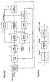
- the signal processing apparatus comprises a gain offset unit 10 which gives a gain based on an inputted control signal and a DC offset based on an inputted offset control signal, to an input reproduction signal; an A/D converter 3 which receives the output signal from the gain offset unit 10, and subjects the signal to sampling with a clock of a predetermined clock cycle T, and analog-to-digital conversion, thereby to output sampling data; a peak detector 4 which receives the sampling data outputted from the A/D converter 3, and performs peak detection from the data with a clock having a cycle n times (n: positive integer) as long as the clock cycle T; a bottom detector 5 which receives the sampling data from the A/D converter 3, and performs bottom detection from the data with a clock having a cycle n times (n: positive integer) as long as the clock cycle T; an amplitude detector 6 which receives output signals from the peak detector 4 and the bottom detector 5, and calculates a signal amplitude at the input of the A/D converter 3 to output an amplitude information signal; an offset detector
- a reproduction signal from the information recording medium is given a gain and an offset based on inputted control signals by the gain offset unit 10, and thereafter, it is sampled with a clock having a predetermined clock cycle T and then converted into a quantized digital signal by the A/D converter 3. Then, the digital signal is subjected to peak detection and bottom detection by the peak detector 4 and the bottom detector 5, respectively.
- the peak detector 4 is composed of a selector 13, a register 14 for temporarily holding the peak value, a subtracter 15, and a comparator 16, as shown in figure 2.
- the comparator 16 compares the present sampling value with the sampling value that is by one sample previous to the present sampling value, which previous value is stored in the register 14.
- the present sampling value When the present sampling value is larger than the previous sampling value, the present sampling value is stored in the register 14. Otherwise, the register 14 is not rewritten. A peak of the digital signal is detected by continuously performing this operation. However, the peak detector 4 merely detects a maximum value, and it cannot follow a fluctuation of the amplitude of the reproduction signal in the amplitude reducing direction. So, the subtracter 15 subtracts a predetermined value from the value stored in the register 14 at regular clock intervals, and the value of the register 14 is replaced with the output of the subtracter 15 when the present sampling value is smaller than the output from the subtracter 15.
- circles ( ⁇ ) indicate the sampling values from the A/D converter 3
- triangles ( ⁇ ) indicate the manner of subtracting a predetermined value at every one clock after peak detection. It is desired that the amount of subtraction should be set to an extent that can follow the signal drop rate of the reproduction signal when passing through the dropout portion. Further, while in this first embodiment both of peak detection and bottom detection are carried out with the same clock as that used by the A/D converter 3, the clock to be used for peak detection and bottom detection is not restricted thereto.
- the operation of the bottom detector 5 is realized by reversing the polarity of the operation of the peak detector 4.
- the amplitude detector 6 and the offset detector 7 perform amplitude detection and offset detection, respectively, on the basis of the detected peak value and the detected bottom value. For example, amplitude detection is carried out by calculating a difference between the peak value and the bottom value, and offset detection is carried out by calculating the sum of the peak value and the bottom value or a difference in distances from the A/D center level, or by detecting whether the peak value and the bottom value are respectively within predetermined window ranges.
- the controller 12 compares the detected amplitude value with a target amplitude value, and controls the gain offset unit 10 so as to increase the gain of the gain offset unit 10 when the detected amplitude value is smaller than the target value.
- the controller 12 controls the gain offset unit 10 so as to reduce the gain of the gain offset unit 10.
- the controller 12 compares the detected amplitude value with a target amplitude value, and controls the gain offset unit 10 so as to increase the output signal amplitude of the gain offset unit 10 when the detected amplitude value is smaller than the target value.
- the controller 12 controls the gain offset unit 10 so as to reduce the output signal amplitude of the gain offset unit 10.
- the controller 12 compares the detected offset value with a target offset value, and controls the gain offset unit 10 so as to increase the output signal offset of the gain offset unit 10 when the detected offset value is smaller than the target value.
- the controller 12 controls the gain offset unit 10 so as to reduce the output signal offset of the gain offset unit 10.
- the dropout detector 11 detects a dropout of the reproduction signal by binarizing the output signal from the peak detector 4 with a predetermined threshold, and outputs a dropout detection signal. Using the dropout detection signal from the dropout detector 11, the control operation of the controller 12 is compulsory held or the control response speed is lowered, whereby excessive response as shown in figure 23(b) is suppressed to obtain a waveform as shown in figure 24(b).
- holding of the controller 12 or switching of the control response speed is carried out on the basis of the output signal from the dropout detector 11, it may be carried out on the basis of a signal generated by, for example, detecting a dropout outside the signal processing apparatus. Alternatively, it may be carried out on the basis of a signal supplied from the outside not when a dropout is detected but when holding of the control operation is desired.
- the dropout detector 11 receives the output signal from the A/D converter 3, it may receive at least one of the output signal from the A/D converter 3, the output signal from the bottom detector 5, the output signal from the offset detector 7, and the amplitude information signal.
- the signal processing circuit may be provided with a through path 10a, i.e., a path which bypasses the gain offset unit 10, and the amplitude information signal may be transmitted through this path 10a and inputted to the A/D converter 3 via a switch 3a, whereby absolute value information of the signal amplitude of the input reproduction signal can be obtained.
- a through path 10a i.e., a path which bypasses the gain offset unit 10
- the amplitude information signal may be transmitted through this path 10a and inputted to the A/D converter 3 via a switch 3a, whereby absolute value information of the signal amplitude of the input reproduction signal can be obtained.
- Many optical disc players and the like employ absolute value information of signal amplitude of a reproduction signal to determine the disc type, and the construction shown in figure 17 enables measurement of signal amplitude without passing the signal through the gain offset unit in these cases.
- a second embodiment of the present invention corresponds to Claims 3, 4, 16, and 18, and shows specific constructions of the gain offset unit and the controller according to the first embodiment.
- Figures 4(a) and 4(b) are block diagrams illustrating a signal processing apparatus according to the second embodiment.
- the signal processing apparatus comprises a variable gain amplifier 1 which gives a gain based on an inputted gain control signal to an input reproduction signal; an offset unit 2 which receives the output signal from the variable gain amplifier 1, and gives a DC offset based on an inputted offset control signal to the signal from the variable gain amplifier 1; an A/D converter 3 which receives the output signal from the offset unit 2, and subjects the signal to sampling with a clock having a predetermined clock cycle T, and A/D conversion, thereby to output sampling data; a peak detector 4 which receives the output signal from the A/D converter 3, and performs peak detection from the signal using a clock having a cycle n times (n: positive integer) as long as the clock cycle T; a bottom detector 5 which receives the output signal from the A/D converter 3, and performs bottom detection from the signal using a clock having a cycle n times (n: positive integer) as long as the clock cycle T; an amplitude detector 6 which receives the output signals from the peak detector 4 and the
- variable gain amplifier 1 and the offset unit 2 correspond to the gain offset unit 10 of the first embodiment
- the gain controller 8 and the offset controller 9 correspond to the controller 12 of the first embodiment.
- the gain controller 8 may be composed of a comparator 8a which compares an input signal with a predetermined target value; an integration counter 8b which is up/down changeable according to the polarity of the output signal from the comparator 8a; and a D/A converter 8c which receives the output signal from the integration counter 8b, and performs D/A conversion of the signal.
- the D/A converter 8c outputs a control signal for controlling the gain of the variable gain amplifier 1.
- the offset controller 9 is constituted similarly to the gain controller 8, and it outputs a control signal for controlling the amount of offset of the offset unit 2.
- variable gain amplifier 1 gives a gain based on a gain control signal to a reproduction signal from the information recording medium
- the offset unit 2 gives an offset based on an offset control signal to the reproduction signal.
- the A/D converter 3 samples the reproduction signal with a clock having a predetermined clock cycle T by the A/D converter 3 to convert the signal into a quantized digital signal.
- the peak detector 4 and the bottom detector 5 perform peak detection and bottom detection from the digital signal, respectively.
- the peak detection and bottom detection are identical to those described for the first embodiment, and both of them may be carried out with a clock having the same cycle as the predetermined clock cycle T.
- a clock having a cycle n times (n: positive integer) as long as the clock cycle T may be used as shown in figure 4, or clocks having cycles which are m times and n times (m,n: mutually independent positive integers) as long as the cycle T may be used for peak detection and bottom detection, respectively, thereby reducing power consumption.
- the amplitude detector 6 performs amplitude detection
- the offset detector 7 performs offset detection, on the basis of the detected peak value and the detected bottom value. For example, amplitude detection is carried out by calculating a difference between the peak value and the bottom value, and offset detection is carried out by calculating the sum of the peak value and the bottom value or a difference in distances from the A/D center level, or by detecting whether or not the peak value and the bottom value are respectively within predetermined window ranges.
- the gain controller 8 compares the detected amplitude value with a target amplitude value, and controls the variable gain amplifier 1 so as to increase the gain of the amplifier 1 when the detected value is smaller than the target value.
- the gain controller 8 controls the variable gain amplifier so as to reduce the gain. Further, the gain controller 8 compares the detected amplitude value with a target amplitude value, and controls the variable gain amplifier 1 so as to increase the output signal amplitude of the amplifier 1 when the detected value is smaller than the target value. Conversely, when the detected value is larger than the target value, the gain controller 8 controls the variable gain amplifier 1 so as to reduce the output signal amplitude. Furthermore, the offset controller 9 compares the detected offset value with a target offset value, and controls the offset unit 2 so as to increase the output signal offset of the offset unit 2 when the detected offset value is smaller than the target value.
- the offset controller 9 controls the offset unit 2 so as to reduce the output signal offset.
- the dropout detector 11 binarizes the output signal from the peak detector 4 with a predetermined threshold value to detect a dropout of the reproduction signal, and compulsory holds the operation of the controller 12 or decreases the control response speed using this signal, whereby excessive response as shown in figure 23(b) is suppressed to obtain a waveform as shown in figure 24(b).
- the gain control or offset control is held or the control response speed is changed on the basis of the fluctuation, thereby suppressing the phenomenon that the reproduction signal which has passed through the defect portion exceeds the input dynamic range of the A/D converter 3. Accordingly, the signal amplitude and offset at the input of the A/D converter 3 can always be kept constant, thereby avoiding the problem that data playback cannot be normally carried out because of a wasted time from when the reproduction signal has passed through the signal dropout (defect) portion to when the signal enters in the input dynamic range of the A/D converter 3 to be pulled into the normal state.
- dropout detection signal is not interrupted during the dropout period as shown in figure 23(c)
- dropout detection can be correctly carried out as shown in figure 24(c), and therefore, it is effective when the signal processing apparatus employs a construction that detects a dropout after A/D conversion.
- holding of the gain controller 8 or switching of the control response speed is carried out on the basis of the output signal from the dropout detector 11, it may be carried out on the basis of a signal that is generated by detecting a dropout outside the signal processing apparatus. Alternatively, it may be carried out on the basis of a signal that is supplied from the outside not when a dropout is detected but when holding of the control operation is desired.
- the dropout detector 11 receives the output signal from the peak detector 4, it may receive at least one of the output signal from the peak detector 4, the output signal from the A/D converter 3, the output signal from the bottom detector 5, the output signal from the offset detector 7, and the amplitude information signal.
- the signal processing circuit may be provided with a through path 1a, i.e., a path which bypasses the variable gain amplifier 1, and the amplitude information signal may be transmitted through this path and inputted to the A/D converter 3 via a switch 2a, whereby absolute value information of the signal amplitude of the input reproduction signal can be obtained.
- a through path 1a i.e., a path which bypasses the variable gain amplifier 1
- the amplitude information signal may be transmitted through this path and inputted to the A/D converter 3 via a switch 2a, whereby absolute value information of the signal amplitude of the input reproduction signal can be obtained.
- Many optical disc players and the like employ absolute value information of signal amplitude of a reproduction signal to determine the disc type, and the structure shown in figure 18 enables measurement of signal amplitude without passing the signal through the variable gain amplifier in these cases.
- a third embodiment of the present invention corresponds to Claim 5, wherein a clock generated from an input reproduction signal is used as a sampling clock.
- Figure 5 is a block diagram illustrating a signal processing apparatus according to the third embodiment.
- the signal processing apparatus is provided with a gain offset unit 10 which gives a gain based on an inputted gain control signal and a DC offset based on an inputted offset control signal to an input reproduction signal; an A/D converter 3 which receives the output signal from the gain offset unit 10, and subjects the signal to sampling with a clock having a predetermined clock cycle T, and A/D conversion, thereby to output sampling data; a peak detector 4 which receives the output signal from the A/D converter 3, and performs peak detection using a clock having a cycle n times (n: positive integer) as long as the clock cycle T; a bottom detector 5 which receives the output signal from the A/D converter 3, and performs bottom detection using a clock having a cycle n times (n: positive integer) as long as the clock cycle T; an amplitude detector 6 which receives the output signals from the peak detector 4 and the bottom detector 5, and calculates a signal amplitude at the input of the A/D converter 3 to output an amplitude information signal; an offset detector 7 which receives the output signals from
- the gain offset unit 10 gives a gain and an offset based on inputted control signals to a reproduction signal from the information recording medium, and the A/D converter 3 samples the reproduction signal with a clock outputted from the PLL unit 17 to convert the signal into a quantized digital signal.
- the peak detector 4 and the bottom detector 5 perform peak detection and bottom detection from the digital signal, respectively.
- the peak detection and bottom detection are identical to those described for the first embodiment. That is, both of them may be carried out using a clock having the same cycle as the predetermined clock cycle T.
- a clock having a cycle n times (n: positive integer) as long as the clock cycle T may be used as shown in figure 5, or clocks having cycles which are m times and n times (m,n: mutually independent positive integers) as long as the cycle T may be used for peak detection and bottom detection, respectively, thereby to reduce power consumption.
- the amplitude detector 6 and the offset detector 7 perform amplitude detection and offset detection on the basis of the detected peak value and the detected bottom value, respectively.
- amplitude detection is carried out by calculating a difference between the peak value and the bottom value
- offset detection is carried out by calculating the sum of the peak value and the bottom value or a difference in distances from the A/D center level, or by detecting whether or not the peak value and the bottom value are respectively within predetermined window ranges.
- the operation of the controller 12 is identical to that described for the first embodiment, and the controller 12 controls the gain offset unit 10 so that the output amplitude and the offset attain the predetermined target values, on the basis of the detected amplitude value and the detected offset value, respectively.
- the PLL unit 17 extracts a clock component possessed by the reproduction signal, and a clock so generated is used as a sampling clock of the A/D converter 3.
- the PLL unit 17 extracts phase error information from the sampling data outputted from the A/D converter 3, and drives a voltage-controlled oscillator or the like on the basis of the error information to generate a phase-locked clock.
- the sampling speed of the A/D converter 3 automatically changes according to the reproduction speed, and the time constants of peak detection and bottom detection also change adaptively to the change of the sampling speed, whereby application to CAV playback is facilitated.
- the operation clock for the peak detector 4 and the bottom detector 5 is set to 1/n (n: positive integer) of the PLL clock, the operating clock frequency is reduced, resulting in a reduction in power consumption. Therefore, the signal amplitude and offset at the input of the A/D converter 3 can always be kept approximately constant, resulting in stable A/D conversion.
- a fourth embodiment of the present invention corresponds to Claims 6 and 7, wherein an oscillation frequency of a playback clock is fixed when detecting a dropout or the like.
- Figure 6 is a block diagram illustrating a signal processing apparatus according to the fourth embodiment.
- the signal processing apparatus comprises a gain offset unit 10 which gives a gain based on an inputted gain control signal and a DC offset based on an inputted offset control signal to an input reproduction signal; an A/D converter 3 which receives the output signal from the gain offset unit 10, and subjects the signal to sampling with a clock having a predetermined clock cycle T, and A/D conversion, thereby to output sampling data; a peak detector 4 which receives the output signal from the A/D converter 3, and performs peak detection with a clock having a cycle n times (n: positive integer) as long as the clock cycle T; a bottom detector 5 which receives the output signal from the A/D converter 3, and performs bottom detection with a clock having a cycle n times (n: positive integer) as long as the clock cycle T; an amplitude detector 6 which receives the output signals from the peak detector 4 and the bottom detector 5, and calculates a signal amplitude at the input of the A/D converter 3 to output an amplitude information signal; an offset detector 7 which receives the output signals from the peak
- the gain offset unit 10 gives a gain and an offset based on inputted control signals to a reproduction signal from the information recording medium, and then the A/D converter 3 samples the reproduction signal with a clock outputted from the PLL unit 17 to convert the signal into a quantized digital signal. Then, the peak detector 4 and the bottom detector 5 perform peak detection and bottom detection from the digital signal, respectively.
- the peak detection and bottom detection are identical to those described for the first embodiment, that is, both of them are carried out with a clock having the same cycle as the predetermined clock cycle T.
- a clock having a cycle n times (n: positive integer) as long as the clock cycle T may be used as shown in figure 6, or clocks having cycles which are m times and n times (m,n: mutually independent positive integers) as long as the cycle T may be used for peak detection and bottom detection, respectively, thereby to reduce power consumption.
- the amplitude detector 6 performs amplitude detection
- the offset detector 7 performs offset detection, on the basis of the detected peak value and the detected bottom value.
- amplitude detection is carried out by calculating a difference between the peak value and the bottom value
- offset detection is carried out by calculating the sum of the peak value and the bottom value or a difference in distances from the A/D center level, or by detecting whether the peak value and the bottom value are within predetermined window ranges or not.
- the operation of the controller 12 is identical to that described for the first embodiment, and the controller 12 controls the gain offset unit 10 so that the output amplitude and offset of the gain offset unit 10 attain the predetermined target values, on the basis of the detected amplitude value and the detected offset value.
- the PLL unit 17 extracts a clock component possessed by the reproduction signal, and a clock so generated is used as a sampling clock of the A/D converter 3.
- the PLL unit 17 extracts phase error information from the sampling data outputted from the A/D converter 3, and generates a PLL clock by driving a voltage controlled oscillator or the like on the basis of the error information.
- the control operation of the controller 12 is compulsory held or the control response speed is decreased by the signal obtained in the dropout detector 11, and the sampling clock frequency outputted from the PLL unit 17 is held or the frequency response speed is decreased.
- the sampling speed of the A/D converter 3 automatically changes according to the playback speed, whereby application to CAV playback is facilitated. Further, since the frequency of the operation clock for the peak detector 4 and the bottom detector 5 is set to 1/n (n: positive integer) of the frequency of the PLL clock, the operation clock frequency is reduced, resulting in a reduction in power consumption.
- the sampling clock can be kept stable, and the signal amplitude and offset at the input of the A/D converter 3 can always be kept approximately constant, thereby avoiding the problem that data reproduction cannot be normally carried out because of a wasted time from when the reproduction signal has passed through the signal dropout portion to when it enters in the input dynamic range of the A/D converter 3 to be pulled into the normal state.
- dropout detection signal is not interrupted during the dropout period as shown in figure 23(c)
- dropout detection can be correctly carried out as shown in figure 24(c), and therefore, it is effective in a system which detects a dropout after A/D conversion.
- holding of the controller 12 or switching of the control response speed is carried out on the basis of the output signal from the dropout detector 11, it may be carried out on the basis of a signal generated by detecting a dropout outside the signal processing apparatus. Alternatively, it may be carried out on the basis of a signal supplied from the outside not when a dropout is detected but when holding of the control operation is desired.
- the dropout detector 11 receives the output signal from the peak detector 4, it may receive at least one of the output signal from the peak detector 4, the output signal from the A/D converter 3, the output signal from the bottom detector 5, the output signal from the offset detector 7, and the amplitude information signal.
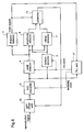
- a fifth embodiment of the present invention corresponds to Claim 8 and Claim 17, which enables data reproduction from different recording areas in the same signal processing system.
- Figure 7 is a block diagram illustrating a signal processing apparatus according to the fifth embodiment.
- the signal processing apparatus comprises a gain offset unit 10 which gives a gain based on an inputted gain control signal and a DC offset based on an inputted offset control signal to a first reproduction signal; an A/D converter 3 which receives the output signal from the gain offset unit 10 and a clock, subjects the signal to sampling with a clock having a predetermined clock cycle T, and A/D conversion, thereby to output sampling data; a peak detector 4 which receives the output signal from the A/D converter 3, and performs peak detection from the signal; a bottom detector 5 which receives the output signal from the A/D converter 3, and performs bottom detection from the signal; an amplitude detector 6 which receives the output signals from the peak detector 4 and the bottom detector 5, and calculates a signal amplitude at the input of the A/D converter 3 to output an amplitude information signal; an offset detector 7 which receives the output signals from the peak detector 4 and the bottom detector 5, and calculates a signal offset at the input of the A/D converter 3 to output an offset information signal; a gate signal generator 18
- the gain offset unit 10 gives a gain and an offset based on inputted control signals to a first reproduction signal from the information recording medium, and thereafter, the A/D converter 3 samples the first reproduction signal with a clock having a predetermined clock cycle T to convert it into a quantized digital signal. Then, the peak detector 4 and the bottom detector 5 perform peak detection and bottom detection from the digital signal, respectively.
- the peak detection and bottom detection are identical to those of the first embodiment, that is, both of them may be carried out with a clock having the same cycle as the predetermined clock cycle T.
- both of peak detection and bottom detection may be performed with a clock having a cycle n times (n: positive integer) as long as the cycle T, or peak detection and bottom detection may be respectively performed with clocks having cycles which are m times and n times (m,n: mutually independent positive integers) as long as the cycle T, thereby to reduce power consumption.
- amplitude detection is carried out by the amplitude detector 6 and offset detection is carried out by the offset detector 7, on the basis of the detected peak value and the detected bottom value.
- amplitude detection is carried out by calculating a difference between the peak value and the bottom value
- offset detection is carried out by calculating the sum of the peak value and the bottom value or a difference in distances from the A/D center level, or by detecting whether the peak value and the bottom value are respectively within predetermined window ranges or not.
- the operation of the controller 12 is identical to that described for the first embodiment, and the controller 12 controls the gain offset unit 10 so that the output amplitude and offset of the gain offset unit 10 attain the predetermined target values, on the basis of the detected amplitude value and the detected offset value.
- the second reproduction signal is input to the gate signal generator 18 to recognize the area information of the optical disc medium.
- the operation of the gate signal generator will be described taking a DVD-RAM as an example.
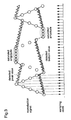
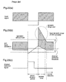
- Figure 8 shows a physical format of a DVD-RAM.
- This physical format is composed of an address area formed of pre-pits, and a rewritable data area.
- the data area is composed of a land section put between two groove sections, and the address area has headers 1 to 4 each by two.
- Each pre-pit is formed in a position that is offset from the center of track.
- This difference signal is the second reproduction signal, and it is passed through a low-pass filter to obtain a signal as shown in figure 10(b).
- the signal shown in figure 10(b) is binarized with predetermined two binarization levels, signals shown in figures 10(c) and 10(d) are obtained.
- these signals are logically added ((c)+(d)), a gate signal indicating an address position is obtained as shown in figure 10(e).
- the controller 12 performs gain/offset control in the address area, when the reproduction signal shifts from the address area to the data area, i.e., when the gate signal shown in figure 10(e) changes from "H” to "L", the gain/offset control values are temporarily stored in the first storage unit 19, and the values stored in the second storage unit 20 are given as gain and offset control values to perform gain and offset control. Therefore, even when the first reproduction signal that is the sum of the signal (a)+(b) obtained from the inside detectors and the signal (c)+(d) obtained from the outside detectors is as shown in figure 11(a), the address area and the data area are independently gain/offset controlled, resulting in a signal as shown in figure 11(b) at the input of the A/D converter 3.
- different recording areas are detected to generate a gate signal, and gain control and offset control are carried out independently for each recording area, thereby to absorb a difference in signal amplitudes and a difference in offsets between the recording areas.
- the signal amplitude and offset at the input of the A/D converter can always be kept constant, and the different recording areas can be reproduced using a single signal processing system.
- a gate signal generated by the gate generator 18 is employed, a signal detected outside the signal processing apparatus may be employed. Further, it may be a signal supplied from the outside not when the area information of the second reproduction signal is recognized but when switching between gain control and offset control is desired.
- a sixth embodiment of the present invention corresponds to Claims 9, 10, and 11, and shows specific constructions of the gain offset unit and the controller according to the fifth embodiment.
- Figure 12 is a block diagram illustrating a signal processing apparatus according to the sixth embodiment.
- This signal processing apparatus comprises a variable gain amplifier 1 which gives a gain based on an inputted gain control signal to an inputted first reproduction signal; an offset unit 2 which receives the output signal from the variable gain amplifier 1, and gives a DC offset based on an inputted offset control signal to the signal; an A/D converter 3 which receives the output signal from the offset unit 2 and a clock, and subjects the signal to sampling with the clock having a predetermined clock cycle T, and analog-to-digital conversion, thereby to output sampling data; a peak detector 4 which receives the output signal from the A/D converter 3, and performs peak detection with a clock having a cycle n times (n: positive integer) as long as the clock cycle T; a bottom detector 5 which receives the output signal from the A/D converter 3, and performs bottom detection with a clock having a cycle n times (n: positive integer) as long as the clock cycle T; an amplitude detector 6 which receives the output signals from the peak detector 4 and the bottom detector 5, and calculates a signal amplitude at the input
- variable gain amplifier 1 and the offset unit 2 correspond to the gain offset unit 10 of the fifth embodiment
- the gain controller 8 and the offset controller 9 correspond to the controller 12 of the first embodiment.
- variable gain amplifier 1 gives a gain based on an inputted gain control signal to a first reproduction signal
- the offset unit 2 gives an offset based on an inputted offset control signal to the first reproduction signal.
- the A/D converter 3 samples the reproduction signal with a clock having a predetermined clock cycle T to convert it into a quantized digital signal.
- the peak detector 4 and the bottom detector 5 perform peak detection and bottom detection from the digital signal, respectively.
- the peak detection and bottom detection are identical to those described for the first embodiment, and both of them may be carried out with a clock having the same cycle as the predetermined clock cycle T.
- both of peak detection and bottom detection may be carried out with a clock having a cycle n times (n: positive integer) as long as the clock cycle T, or peak detection and bottom detection may be respectively carried out with clocks having cycles that are m times and n times (m,n: mutually independent positive integers) as long as the clock cycle T, thereby to reduce power consumption.
- the gain and offset control operations of the gain controller 8 and the offset controller 9 are identical to those described for the first embodiment.
- the second reproduction signal is input to the gate signal generator 18, and the gate signal generator 18 recognizes area information on the optical disc medium. While the gain controller 8 performs gain control on the address area, when the reproduction signal shifts from the address area to the data area, it stores the gain control value temporarily in the first gain storage unit 22, and gives a value stored in the second gain storage unit 23 as a gain control value to perform gain control.
- different reading areas are detected to generate a gate signal, and gain control and offset control are carried out independently for each recording area, thereby to absorb a difference in signal amplitudes and a difference in offsets between the recording areas.
- gain control and offset control are carried out independently for each recording area, thereby to absorb a difference in signal amplitudes and a difference in offsets between the recording areas.
- a gate signal generated by the gate generator 18 is employed, a signal detected outside the signal processing apparatus may be employed. Further, it may be a signal supplied from the outside not when the area information of the second reproduction signal is recognized but when switching of gain/offset control is desired.
- gain and offset controls are carried out independently for each area, only gain control or offset control may be carried out independently in accordance with each recording area.
- a seventh embodiment of the present invention corresponds to Claim 12, wherein an equalizer for equalizing a signal is provided in a stage previous to the A/D converter.
- Figure 13 is a block diagram illustrating a signal processing apparatus according to the seventh embodiment.
- This signal processing apparatus comprises a gain offset unit 10 which gives a gain based on an inputted gain control signal and a DC offset based on an inputted offset control signal to an input reproduction signal; an equalizer 26 which receives the output signal from the gain offset unit 10, and emphasizes high-frequency bands of the signal; an A/D converter 3 which receives the output signal from the equalizer 26, and subjects the signal to sampling with a clock having a predetermined clock cycle T, and analog-to-digital conversion, thereby to output sampling data; a peak detector 4 which receives the output signal from the A/D converter 3, and performs peak detection with a clock having a cycle n times (n: positive integer) as long as the clock cycle T; a bottom detector 5 which receives the output from the A/D converter 3, and performs bottom detection with a clock having a cycle n times (n: positive integer) as long as the clock cycle T; an amplitude detector 6 which receives the output signals from the peak detector 4 and the bottom detector 5, and calculates a signal amplitude at the input of
- the gain offset unit 10 gives a gain and an offset based on inputted control inputs to a reproduction signal from the information recording medium, and then the equalizer 26 subjects the signal to waveform equalization.
- the equalizer 26 When playing a high-density optical recording medium or the like, since the signal amplitude of a short recording mark is lowered due to optical frequency characteristics, it is necessary to boost up this frequency band by the equalizer 26 to improve the SNR (Signal to Noise Ratio) of the signal. Further, the output signal from the equalizer 26 is sampled with a clock having a predetermined clock cycle T, and converted into a quantized digital signal by the A/D converter 3.
- the peak detector 4 and the bottom detector 5 perform peak detection and bottom detection from the digital signal, respectively.
- the peak detection and bottom detection are identical to those described for the first embodiment, and both of them may be carried out with a clock having the same cycle as the predetermined clock cycle T. However, as shown in figure 13, both of peak detection and bottom detection may be carried out with a clock having a cycle n times (n: positive integer) as long as the clock cycle T, or peak detection and bottom detection may be respectively carried out with clocks having cycles that are m times and n times (m,n: mutually independent positive integers) as long as the clock cycle T, thereby to reduce power consumption.
- the amplitude detector 6 performs amplitude detection
- the offset detector 7 performs offset detection, on the basis of the detected peak value and the detected bottom value.
- the amplitude detection and offset detection are identical to those described for the first embodiment.
- the controller 12 performs gain/offset control on the gain/offset unit 10 so that the detected amplitude value and the detected offset value become equal to their target values, respectively.
- the control operation is identical to that described for the first embodiment.
- the input signal amplitude and the input signal offset to the equalizer 26 can be controlled to be constant, whereby the signal amplitude and the input signal offset can be kept constant.
- the maximum SNR can be attained, and it becomes unnecessary to consider a margin for a deviation such as a circuit offset that occurs in the stage previous to the equalizer 26, whereby the signal can be input to the equalizer 26 at the maximum amplitude within the dynamic range of the equalizer 26.
- the signal when the signal amplitude is not increased due to a short pit formed on the optical disc, the signal does not attain the saturated amplitude as shown by the solid line in figure 14. If there is no equalizer, a peak (or a bottom) of the input reproduction signal due to this short pit cannot be correctly detected.
- the equalizer 26 since the equalizer 26 is provided in this seventh embodiment, the signal attains the saturated state as shown by the dashed line in figure 14 even when the pit length is short, whereby peak detection (or bottom detection) can be carried out correctly, resulting in an increase in precision of gain control or offset control.
- An eighth embodiment of the present invention corresponds to Claim 13, wherein the gain offset unit according to the seventh embodiment is divided into two sub-blocks, and an equalizer is placed between them.
- Figure 15 is a block diagram illustrating a signal processing apparatus according to the eighth embodiment.
- the signal processing apparatus comprises a variable gain amplifier 1 which gives a gain based on an inputted gain control signal to an input reproduction signal; an equalizer 26 which receives the output signal from the variable gain amplifier 1, and emphasizes high frequency bands of the input signal; an offset unit 2 which receives the output signal from the equalizer 26, and gives a DC offset based on an inputted offset control signal to the input signal; an A/D converter 3 which receives the output signal from the offset unit 2, subjects the signal to sampling with a clock having a predetermined clock cycle T, and analog-to-digital conversion, thereby to output sampling data; a peak detector 4 which receives the output signal from the A/D converter 3, and subjects the signal to peak detection with a clock having a cycle n times (n: positive integer) as long as the clock cycle T; a bottom detector 5 which receives the output signal from the A/D converter 3, and subjects the signal to bottom detection with a clock having a cycle n times (n: positive integer) as long as the clock cycle T; an amplitude detector 6 which receives the
- variable gain amplifier 1 and the offset unit 2 correspond to the gain offset unit 10 of the seventh embodiment
- the gain controller 8 and the offset controller 9 correspond to the controller 12 of the seventh embodiment.
- variable gain amplifier 1 gives a gain based on an inputted gain control signal to a reproduction signal from the information recording medium
- the equalizer 26 subjects the reproduction signal to waveform equalization
- the offset unit 2 gives an offset based on an inputted offset control signal to the reproduction signal.
- the equalizer 26 When playing a high-density optical recording medium or the like, since the signal amplitude of a short recording mark is undesirably lowered due to optical frequency characteristics, it is necessary to boost up this frequency band with the equalizer 26 to improve the SNR (Signal to Noise Ratio) of the signal. Further, the output signal from the equalizer 26 is sampled with a clock having a predetermined clock cycle T by the A/D converter 3 and then converted into a quantized digital signal. The peak detector 4 and the bottom detector 5 perform peak detection and bottom detection from this digital signal, respectively. The peak detection and bottom detection are identical to those described for the first embodiment, and both of them may be performed with a clock having the same cycle as the predetermined clock cycle T.
- both of peak detection and bottom detection may be carried out with a clock having a cycle that is n times (n: positive integer) as long as the clock cycle T, or peak detection and bottom detection may be respectively carried out with clocks having cycles that are m times and n times (m,n: mutually independent positive integers) as long as the clock cycle T, thereby to reduce power consumption.
- the amplitude detector 6 performs amplitude detection
- the offset detector 7 performs offset detection, on the basis of the detected peak value and the detected bottom value.
- the amplitude detection and offset detection are identical to those described for the first embodiment.
- the gain and offset control operations of the gain controller 8 and the offset controller 9 are identical to those described for the second embodiment.
- the equalizer 26 is placed after the variable gain amplifier 1 in this eighth embodiment, the signal amplitude can be controlled to be constant, and it becomes unnecessary to consider a margin for a circuit gain deviation that occurs at the stage previous to the equalizer 26, whereby the signal can be input to the equalizer 26 at the maximum amplitude within the dynamic range of the equalizer 26. Further, since the equalizer 26 is provided in this eighth embodiment, the signal attains the saturated state as shown by the dashed line in figure 14 even when the pit length is short, whereby peak detection (or bottom detection) can be carried out correctly, resulting in an increase in precision of gain control or offset control.
- a ninth embodiment of the present invention corresponds to Claim 14, in which the offset unit and the equalizer are interchanged.
- Figure 16 is a block diagram illustrating a signal processing apparatus according to the ninth embodiment.
- This signal processing apparatus comprises a variable gain amplifier 1 which gives a gain based on an inputted gain control signal to an input reproduction signal; an offset unit 2 which receives the output signal from the variable gain amplifier 1, and gives a DC offset based on an inputted offset control signal to the input signal; an equalizer 26 which receives the output signal from the offset unit 2, and emphasizes high frequency bands of the input signal; an A/D converter 3 which receives the output signal from the equalizer 26, and subjects the signal to sampling with a clock having a predetermined clock cycle T, and analog-to-digital conversion, thereby to output sampling data; a peak detector 4 which receives the output signal from the A/D converter 3, and subjects the signal to peak detection with a clock having a cycle n times (n: positive integer) as long as the clock cycle T; a bottom detector 5 which receives the output signal from the A/D converter 3, and subjects the signal to bottom detection with a clock having a cycle n times (n: positive integer) as long as the clock cycle T; an amplitude detector 6 which receives
- variable gain amplifier 1 and the offset unit 2 correspond to the gain offset unit 10 of the seventh embodiment
- the gain controller 8 and the offset controller 9 correspond to the controller 12 of the seventh embodiment.
- variable gain amplifier 1 gives a gain based on a gain control signal to a reproduction signal from the information recording medium
- the offset unit 2 gives an offset based on an offset control signal to the reproduction signal
- the equalizer 26 subjects the signal to waveform equalization.
- the output signal from the equalizer 26 is sampled with a clock having a predetermined clock cycle T and then converted into a quantized digital signal by the A/D converter 3.
- the peak detector 4 and the bottom detector 5 perform peak detection and bottom detection from this digital signal, respectively.
- the peak detection and bottom detection are identical to those described for the first embodiment, and both of them may be carried out with a clock having the same cycle as the predetermined clock cycle T.
- both of them may be carried out with a clock having a cycle that is n times (n: positive integer) as long as the clock cycle T, or peak detection and bottom detection may be respectively carried out with clocks having cycles that are m times and n times (m,n: mutually independent positive integers) longer than the clock cycle T, thereby to reduce power consumption.
- the amplitude detector 6 and the offset detector 7 perform amplitude detection and offset detection, respectively, on the basis of the detected peak value and the detected bottom value.
- the amplitude detection and offset detection are identical to those described for the first embodiment.
- the gain and offset control operations of the gain controller 8 and the offset controller 9 are identical to those described for the second embodiment.
- the signal amplitude and offset can be controlled to be constant, and it becomes unnecessary to consider margins for gain and offset deviations that occur at the stage previous to the equalizer 26, whereby the signal can be input to the equalizer 26 at the maximum amplitude within the dynamic range of the equalizer 26.
- the equalizer 26 is provided in this ninth embodiment, the signal attains the saturated state as shown by the dashed line in figure 14 even when the pit length is short, whereby peak detection (or bottom detection) can be carried out correctly, resulting in an increase in precision of gain control or offset control.
- a tenth embodiment of the present invention corresponds to Claims 21 and 22, wherein a servo controller is provided.
- Figure 19(a) is a block diagram illustrating a signal processing apparatus according to the tenth embodiment.
- the apparatus according to this tenth embodiment further includes a servo controller 27 which receives the output signal from the amplitude detector 6, and learns the focus control position or tracking control position of a pickup on the basis of the reproduction signal amplitude information.
- Figure 19(a) is a schematic diagram of an optical disc device including the signal processing apparatus, and an optical disc 100 as an information recording medium is driven by a spindle motor (not shown).
- an optical pickup 200 for reading data from the optical disc 100 comprises a laser 201 for emitting a laser beam to irradiate the optical disc 100 with the laser beam; a beam splitter 204 for separating the path of the laser beam emitted from the laser 201 from the path of the laser beam reflected at the optical disc 100; a lens 202 for focusing the laser beam that has passed through the beam splitter 204, onto an information surface of the optical disc 100; an actuator 203 for driving the lens 202 on the basis of a focus control signal and a tracking control signal from the servo controller 27; and a photodetector 205 for light-to-electricity converting the reflected laser beam from the optical disc 100, which has passed through the beam splitter 204, to output a reproduction signal to the gain offset unit 10.
- the servo controller 27 controls the controller 12 to turn on gain control and offset control, thereby to make the signal amplitude constant and secure resolution for A/D conversion (step S1).
- the servo controller 17 instructs the controller 12 to hold gain control (step S2).
- the servo controller 27 instructs the controller 12 to perform focus and tracking learning, for example, learning to maximize the signal amplitude (step S3).
- the servo controller 27 controls the controller 12 to start gain and offset control again.
- the amplitude change in the input reproduction signal is transferred as it is to the output of the amplitude detector by compulsory holding gain control. Further, the amplitude detection operation can be stabilized by holding offset control simultaneously with gain control.
- gain control and offset control are carried out before learning, and learning operation is started after the both controls are completed, whereby the signal amplitude at the input of the A/D converter can be made approximately constant irregardless of the input reproduction signal amplitude, and the sensitivity of learning can be kept constant.
- the reflectivity of DVD-RW media is as low as 1/4 to 1/5 of the reflectivity of DVD-RW media, and the input reproduction signal amplitude becomes smaller, and therefore, the output from the amplitude detector also becomes smaller, resulting in a problem that learning sensitivity cannot be obtained.
- gain control and offset control are carried out before leaning, and the both controls are held to perform learning after setting the input signal amplitude of the A/D converter 3 to a predetermined value. Therefore, it becomes unnecessary to consider the analog input amplitude variation, resulting in stable learning.
Landscapes
- Engineering & Computer Science (AREA)
- Signal Processing (AREA)
- Signal Processing For Digital Recording And Reproducing (AREA)
- Optical Recording Or Reproduction (AREA)
- Analogue/Digital Conversion (AREA)
Applications Claiming Priority (2)
| Application Number | Priority Date | Filing Date | Title |
|---|---|---|---|
| JP2002064879 | 2002-03-11 | ||
| JP2002064879 | 2002-03-11 |
Publications (2)
| Publication Number | Publication Date |
|---|---|
| EP1345221A2 true EP1345221A2 (de) | 2003-09-17 |
| EP1345221A3 EP1345221A3 (de) | 2007-12-26 |
Family
ID=27764458
Family Applications (1)
| Application Number | Title | Priority Date | Filing Date |
|---|---|---|---|
| EP03004984A Withdrawn EP1345221A3 (de) | 2002-03-11 | 2003-03-11 | Signalverarbeitungsgerät und Signalverarbeitungsverfahren |
Country Status (5)
| Country | Link |
|---|---|
| US (1) | US7215632B2 (de) |
| EP (1) | EP1345221A3 (de) |
| JP (1) | JP4081018B2 (de) |
| CN (1) | CN100380497C (de) |
| WO (1) | WO2003077248A1 (de) |
Cited By (3)
| Publication number | Priority date | Publication date | Assignee | Title |
|---|---|---|---|---|
| WO2005057575A1 (en) * | 2003-12-08 | 2005-06-23 | Koninklijke Philips Electronics N.V. | Method and system for controlling the level of a data signal read from an optical disc |
| WO2006132908A1 (en) | 2005-06-03 | 2006-12-14 | Zoran Corporation | Processing an information carrying signal for automatic gain conrtol |
| US7613975B2 (en) * | 2005-02-03 | 2009-11-03 | Hewlett-Packard Development Company, L.P. | Predictive diagnosis of a data read system |
Families Citing this family (35)
| Publication number | Priority date | Publication date | Assignee | Title |
|---|---|---|---|---|
| CN100580788C (zh) * | 2002-12-27 | 2010-01-13 | 松下电器产业株式会社 | 信号处理装置及信号处理方法 |
| KR20060019577A (ko) * | 2003-06-11 | 2006-03-03 | 코닌클리케 필립스 일렉트로닉스 엔.브이. | 광 디스크 드라이브 장치 |
| US7620101B1 (en) * | 2003-09-24 | 2009-11-17 | Cypress Semiconductor Corporation | Equalizer circuit, communication system, and method that is adaptive to varying launch amplitudes for reducing receiver error |
| JP4079902B2 (ja) * | 2004-03-16 | 2008-04-23 | Necエレクトロニクス株式会社 | 光ディスク装置とそのトラッキング制御方法 |
| US7440525B2 (en) * | 2004-08-27 | 2008-10-21 | Mindspeed Technologies, Inc. | Dynamic range signal to noise optimization system and method for receiver |
| KR100652432B1 (ko) | 2005-09-08 | 2006-12-01 | 삼성전자주식회사 | 광디스크 기록/재생 기기의 신호 처리 장치 및 신호 처리방법 |
| US20070058502A1 (en) * | 2005-09-12 | 2007-03-15 | Chi-Pei Huang | Servo system and related method of adjusting the magnitude of detecting signals outputted from a pick-up head before utilizing the detecting signals to generate servo signals |
| US7710851B2 (en) | 2005-09-28 | 2010-05-04 | Panasonic Corporation | Optical disc apparatus |
| JP4130831B2 (ja) * | 2005-10-07 | 2008-08-06 | 松下電器産業株式会社 | 動的dcオフセット除去装置及び動的dcオフセット除去方法 |
| US20070086315A1 (en) * | 2005-10-19 | 2007-04-19 | Mediatek Inc. | Optical disc apparatuses |
| US7684291B2 (en) * | 2006-06-05 | 2010-03-23 | Mediatek Inc. | Method and apparatus for blank detection of an optical disc |
| US7724090B2 (en) * | 2006-06-05 | 2010-05-25 | Mediatek Inc. | Loop control apparatus and method thereof |
| US7796480B2 (en) * | 2006-06-05 | 2010-09-14 | Mediatek Inc. | Apparatus and methods for light spot servo signal detection |
| US20070280079A1 (en) * | 2006-06-05 | 2007-12-06 | Yuh Cheng | Asymmetry measurement apparatus |
| CN101086854B (zh) * | 2006-06-05 | 2011-06-01 | 联发科技股份有限公司 | 回路控制装置及其方法 |
| US8416845B1 (en) * | 2006-07-11 | 2013-04-09 | Altera Corporation | Decision feedback equalization for variable input amplitude |
| US20100046339A1 (en) * | 2006-09-19 | 2010-02-25 | Yoshihiro Kanda | Optical disc recording/reproduction apparatus |
| US20080101795A1 (en) * | 2006-10-27 | 2008-05-01 | Craig Schulz | Data signal amplitude and cross-point detectors in an optical modulator control system |
| JP2008167303A (ja) * | 2006-12-28 | 2008-07-17 | Fujitsu Ltd | データサンプリング回路及びデータサンプリング方法 |
| US8055871B1 (en) | 2007-02-27 | 2011-11-08 | Nvidia Corporation | Low latency synchronous memory performance switching using update control |
| CN101689387A (zh) * | 2007-06-27 | 2010-03-31 | 松下电器产业株式会社 | 信号处理装置 |
| JP2009146491A (ja) * | 2007-12-13 | 2009-07-02 | Hitachi Ltd | 光ディスク装置 |
| US8451949B2 (en) * | 2008-10-07 | 2013-05-28 | Realtek Semiconductor Corp. | Clock-data recovery and method for binary signaling using low resolution ADC |
| JP4697298B2 (ja) * | 2008-12-19 | 2011-06-08 | ソニー株式会社 | コンパレータおよび光ディスク記録再生装置 |
| JP2010147943A (ja) * | 2008-12-19 | 2010-07-01 | Sony Corp | 情報処理装置、及び信号伝送方法 |
| US8442154B2 (en) * | 2009-04-23 | 2013-05-14 | Maxlinear, Inc. | Channel sensitive power control |
| JP4941515B2 (ja) | 2009-07-02 | 2012-05-30 | 富士通株式会社 | 受信回路、オフセット調整方法、及び送受信システム |
| US8830808B1 (en) * | 2009-09-10 | 2014-09-09 | Marvell International Ltd. | Method and apparatus for zero offset and gain start |
| US8081395B1 (en) * | 2009-12-15 | 2011-12-20 | Western Digital Technologies, Inc. | Continuous digital offset cancellation |
| KR20120121779A (ko) * | 2011-04-27 | 2012-11-06 | 삼성전기주식회사 | 자기 검출 회로의 오프셋 보상 장치 및 그 방법 |
| US8929017B2 (en) * | 2011-12-12 | 2015-01-06 | Lsi Corporation | Systems and methods for SNR measurement using equalized data |
| KR101523168B1 (ko) * | 2014-01-27 | 2015-05-26 | 엘에스산전 주식회사 | 아날로그 입력모듈의 오프셋 및 게인 설정 시스템 및 방법 |
| US11064446B2 (en) * | 2016-04-26 | 2021-07-13 | Anatog Devices, Inc. | Apparatus and methods for wideband receivers |
| US9729132B1 (en) * | 2016-07-28 | 2017-08-08 | Nxp B.V. | Precise signal swing squelch detector |
| JP2022059467A (ja) * | 2020-10-01 | 2022-04-13 | 豊田合成株式会社 | 位置検出装置 |
Family Cites Families (17)
| Publication number | Priority date | Publication date | Assignee | Title |
|---|---|---|---|---|
| JP3067298B2 (ja) | 1991-08-09 | 2000-07-17 | ソニー株式会社 | 光ディスクのデータ再生装置と再生方法 |
| JP2768611B2 (ja) * | 1992-12-18 | 1998-06-25 | 株式会社ケンウッド | 光ディスク装置のディフェクト検出回路および光ディスク装置 |
| JP2889803B2 (ja) * | 1993-11-22 | 1999-05-10 | 三洋電機株式会社 | レベル設定回路 |
| JP2674522B2 (ja) * | 1994-09-27 | 1997-11-12 | 日本電気株式会社 | 光ディスク装置における傷検出回路 |
| US5587975A (en) * | 1994-10-24 | 1996-12-24 | Sony Corporation | Magneto-optical disk reproducing apparatus with gain and offset controlled by a reference pattern read from the disk |
| JP3823184B2 (ja) * | 1995-04-05 | 2006-09-20 | 松下電器産業株式会社 | 光ディスク装置 |
| US5777967A (en) * | 1995-04-05 | 1998-07-07 | Matsushita Electric Industrial Co., Ltd. | Optical disk device |
| EP0750306B1 (de) * | 1995-06-22 | 2002-06-05 | Matsushita Electric Industrial Co., Ltd. | Verfahren zur Maximalwahrscheinlichkeitsdekodierung und Gerät zur Wiedergabe von Digitalinformationen |
| JPH1031821A (ja) * | 1996-07-16 | 1998-02-03 | Matsushita Electric Ind Co Ltd | 光ディスク装置 |
| US6069866A (en) * | 1997-10-23 | 2000-05-30 | Cirrus Logic, Inc. | System and method for coarse gain control of wide band amplifiers |
| KR19990051851A (ko) * | 1997-12-20 | 1999-07-05 | 구본준 | 디스크 재생 장치의 리드 회로 |
| US6104682A (en) * | 1998-07-23 | 2000-08-15 | Matsushita Electric Industrial Co., Ltd. | Disk apparatus having a data reproducing system using a digital PLL |
| JP3856418B2 (ja) * | 1998-09-10 | 2006-12-13 | パイオニア株式会社 | 記録媒体プレーヤのサーボ装置 |
| JP3486145B2 (ja) * | 2000-01-17 | 2004-01-13 | 松下電器産業株式会社 | デジタル記録データ再生装置 |
| JP2002015422A (ja) * | 2000-04-26 | 2002-01-18 | Matsushita Electric Ind Co Ltd | 光ディスク装置 |
| US6434098B2 (en) * | 2000-04-26 | 2002-08-13 | Matsushita Electric Industrial Co., Ltd. | Optical disc device |
| JP2002319239A (ja) | 2001-04-20 | 2002-10-31 | Matsushita Electric Ind Co Ltd | 情報再生装置 |
-
2003
- 2003-03-11 WO PCT/JP2003/002835 patent/WO2003077248A1/ja not_active Ceased
- 2003-03-11 US US10/479,275 patent/US7215632B2/en not_active Expired - Fee Related
- 2003-03-11 JP JP2003575380A patent/JP4081018B2/ja not_active Expired - Fee Related
- 2003-03-11 EP EP03004984A patent/EP1345221A3/de not_active Withdrawn
- 2003-03-11 CN CNB038041049A patent/CN100380497C/zh not_active Expired - Fee Related
Cited By (4)
| Publication number | Priority date | Publication date | Assignee | Title |
|---|---|---|---|---|
| WO2005057575A1 (en) * | 2003-12-08 | 2005-06-23 | Koninklijke Philips Electronics N.V. | Method and system for controlling the level of a data signal read from an optical disc |
| US7613975B2 (en) * | 2005-02-03 | 2009-11-03 | Hewlett-Packard Development Company, L.P. | Predictive diagnosis of a data read system |
| WO2006132908A1 (en) | 2005-06-03 | 2006-12-14 | Zoran Corporation | Processing an information carrying signal for automatic gain conrtol |
| US7668053B2 (en) | 2005-06-03 | 2010-02-23 | Zoran Corporation | Processing an information carrying signal |
Also Published As
| Publication number | Publication date |
|---|---|
| EP1345221A3 (de) | 2007-12-26 |
| WO2003077248A1 (en) | 2003-09-18 |
| US20040172148A1 (en) | 2004-09-02 |
| JP4081018B2 (ja) | 2008-04-23 |
| US7215632B2 (en) | 2007-05-08 |
| CN100380497C (zh) | 2008-04-09 |
| JPWO2003077248A1 (ja) | 2005-07-07 |
| CN1633691A (zh) | 2005-06-29 |
Similar Documents
| Publication | Publication Date | Title |
|---|---|---|
| US7215632B2 (en) | Signal processing apparatus and signal processing method | |
| JP3968193B2 (ja) | プリピット検出装置 | |
| JPH08235767A (ja) | 光ディスクプレーヤ | |
| US8022847B2 (en) | Signal processing device | |
| JP2002312941A (ja) | 光記録媒体のプリピット検出装置 | |
| US5831951A (en) | Method and apparatus for controlling a slice signal in the reproduction information recorded in an optical disk | |
| CN1236943A (zh) | 光盘装置 | |
| JPH10215175A (ja) | Pll回路及び信号再生装置 | |
| US7558171B2 (en) | Optical disc recording/playback apparatus | |
| JP3554641B2 (ja) | 光ディスク駆動装置 | |
| KR100507560B1 (ko) | 광 디스크장치 | |
| JP2002237052A (ja) | 光記録媒体のプリピット検出装置 | |
| JP3714117B2 (ja) | プリピット検出装置、プリピット検出方法、位置及び周波数信号の検出回路 | |
| US5796691A (en) | Spindle servo system for adjusting rotational speed in optical disk player | |
| KR20050030168A (ko) | 결점검출장치, 결점검출방법 | |
| CN1573972A (zh) | 光盘装置和光盘处理方法 | |
| KR20010036087A (ko) | 고밀도 디스크 기록매체와 그에 따른 데이터 재생장치 및 방법 | |
| JP3887380B2 (ja) | 光ディスク駆動装置と光ディスク駆動方法 | |
| JP2000067434A (ja) | 位相比較装置 | |
| JPH10283730A (ja) | 光ディスク再生装置および方法 | |
| KR20030053046A (ko) | 광디스크 장치 및 서보 제어 방법 | |
| JPH11213412A (ja) | トラッキングエラー信号の振幅調整装置および光ディスク装置 | |
| JP2002319134A (ja) | 光ディスク記録再生装置および記録タイミング制御方法 | |
| JPH08171746A (ja) | 光ディスク装置 | |
| JPH10214458A (ja) | 光ディスク装置 |
Legal Events
| Date | Code | Title | Description |
|---|---|---|---|
| PUAI | Public reference made under article 153(3) epc to a published international application that has entered the european phase |
Free format text: ORIGINAL CODE: 0009012 |
|
| AK | Designated contracting states |
Kind code of ref document: A2 Designated state(s): AT BE BG CH CY CZ DE DK EE ES FI FR GB GR HU IE IT LI LU MC NL PT SE SI SK TR |
|
| AX | Request for extension of the european patent |
Extension state: AL LT LV MK RO |
|
| PUAL | Search report despatched |
Free format text: ORIGINAL CODE: 0009013 |
|
| AK | Designated contracting states |
Kind code of ref document: A3 Designated state(s): AT BE BG CH CY CZ DE DK EE ES FI FR GB GR HU IE IT LI LU MC NL PT SE SI SK TR |
|
| AX | Request for extension of the european patent |
Extension state: AL LT LV MK RO |
|
| RIC1 | Information provided on ipc code assigned before grant |
Ipc: G11B 7/005 20060101ALI20071122BHEP Ipc: G11B 20/10 20060101AFI20030611BHEP |
|
| 17P | Request for examination filed |
Effective date: 20080218 |
|
| AKX | Designation fees paid |
Designated state(s): DE FR GB |
|
| RAP1 | Party data changed (applicant data changed or rights of an application transferred) |
Owner name: PANASONIC CORPORATION |
|
| STAA | Information on the status of an ep patent application or granted ep patent |
Free format text: STATUS: THE APPLICATION HAS BEEN WITHDRAWN |
|
| 18W | Application withdrawn |
Effective date: 20090825 |