EP1237191A2 - Modules de circuits électroniques à haute densité - Google Patents
Modules de circuits électroniques à haute densité Download PDFInfo
- Publication number
- EP1237191A2 EP1237191A2 EP02076327A EP02076327A EP1237191A2 EP 1237191 A2 EP1237191 A2 EP 1237191A2 EP 02076327 A EP02076327 A EP 02076327A EP 02076327 A EP02076327 A EP 02076327A EP 1237191 A2 EP1237191 A2 EP 1237191A2
- Authority
- EP
- European Patent Office
- Prior art keywords
- layer
- circuit
- circuits
- layers
- silicon
- Prior art date
- Legal status (The legal status is an assumption and is not a legal conclusion. Google has not performed a legal analysis and makes no representation as to the accuracy of the status listed.)
- Withdrawn
Links
Images


Classifications
-
- H—ELECTRICITY
- H10—SEMICONDUCTOR DEVICES; ELECTRIC SOLID-STATE DEVICES NOT OTHERWISE PROVIDED FOR
- H10D—INORGANIC ELECTRIC SEMICONDUCTOR DEVICES
- H10D86/00—Integrated devices formed in or on insulating or conducting substrates, e.g. formed in silicon-on-insulator [SOI] substrates or on stainless steel or glass substrates
- H10D86/01—Manufacture or treatment
- H10D86/021—Manufacture or treatment of multiple TFTs
- H10D86/0214—Manufacture or treatment of multiple TFTs using temporary substrates
-
- A—HUMAN NECESSITIES
- A61—MEDICAL OR VETERINARY SCIENCE; HYGIENE
- A61B—DIAGNOSIS; SURGERY; IDENTIFICATION
- A61B3/00—Apparatus for testing the eyes; Instruments for examining the eyes
- A61B3/10—Objective types, i.e. instruments for examining the eyes independent of the patients' perceptions or reactions
- A61B3/113—Objective types, i.e. instruments for examining the eyes independent of the patients' perceptions or reactions for determining or recording eye movement
-
- G—PHYSICS
- G02—OPTICS
- G02B—OPTICAL ELEMENTS, SYSTEMS OR APPARATUS
- G02B27/00—Optical systems or apparatus not provided for by any of the groups G02B1/00 - G02B26/00, G02B30/00
- G02B27/0093—Optical systems or apparatus not provided for by any of the groups G02B1/00 - G02B26/00, G02B30/00 with means for monitoring data relating to the user, e.g. head-tracking, eye-tracking
-
- G—PHYSICS
- G02—OPTICS
- G02B—OPTICAL ELEMENTS, SYSTEMS OR APPARATUS
- G02B27/00—Optical systems or apparatus not provided for by any of the groups G02B1/00 - G02B26/00, G02B30/00
- G02B27/01—Head-up displays
- G02B27/017—Head mounted
-
- G—PHYSICS
- G02—OPTICS
- G02B—OPTICAL ELEMENTS, SYSTEMS OR APPARATUS
- G02B27/00—Optical systems or apparatus not provided for by any of the groups G02B1/00 - G02B26/00, G02B30/00
- G02B27/01—Head-up displays
- G02B27/017—Head mounted
- G02B27/0172—Head mounted characterised by optical features
-
- G—PHYSICS
- G02—OPTICS
- G02F—OPTICAL DEVICES OR ARRANGEMENTS FOR THE CONTROL OF LIGHT BY MODIFICATION OF THE OPTICAL PROPERTIES OF THE MEDIA OF THE ELEMENTS INVOLVED THEREIN; NON-LINEAR OPTICS; FREQUENCY-CHANGING OF LIGHT; OPTICAL LOGIC ELEMENTS; OPTICAL ANALOGUE/DIGITAL CONVERTERS
- G02F1/00—Devices or arrangements for the control of the intensity, colour, phase, polarisation or direction of light arriving from an independent light source, e.g. switching, gating or modulating; Non-linear optics
- G02F1/01—Devices or arrangements for the control of the intensity, colour, phase, polarisation or direction of light arriving from an independent light source, e.g. switching, gating or modulating; Non-linear optics for the control of the intensity, phase, polarisation or colour
- G02F1/13—Devices or arrangements for the control of the intensity, colour, phase, polarisation or direction of light arriving from an independent light source, e.g. switching, gating or modulating; Non-linear optics for the control of the intensity, phase, polarisation or colour based on liquid crystals, e.g. single liquid crystal display cells
- G02F1/133—Constructional arrangements; Operation of liquid crystal cells; Circuit arrangements
- G02F1/1333—Constructional arrangements; Manufacturing methods
- G02F1/1335—Structural association of cells with optical devices, e.g. polarisers or reflectors
- G02F1/133526—Lenses, e.g. microlenses or Fresnel lenses
-
- G—PHYSICS
- G02—OPTICS
- G02F—OPTICAL DEVICES OR ARRANGEMENTS FOR THE CONTROL OF LIGHT BY MODIFICATION OF THE OPTICAL PROPERTIES OF THE MEDIA OF THE ELEMENTS INVOLVED THEREIN; NON-LINEAR OPTICS; FREQUENCY-CHANGING OF LIGHT; OPTICAL LOGIC ELEMENTS; OPTICAL ANALOGUE/DIGITAL CONVERTERS
- G02F1/00—Devices or arrangements for the control of the intensity, colour, phase, polarisation or direction of light arriving from an independent light source, e.g. switching, gating or modulating; Non-linear optics
- G02F1/01—Devices or arrangements for the control of the intensity, colour, phase, polarisation or direction of light arriving from an independent light source, e.g. switching, gating or modulating; Non-linear optics for the control of the intensity, phase, polarisation or colour
- G02F1/13—Devices or arrangements for the control of the intensity, colour, phase, polarisation or direction of light arriving from an independent light source, e.g. switching, gating or modulating; Non-linear optics for the control of the intensity, phase, polarisation or colour based on liquid crystals, e.g. single liquid crystal display cells
- G02F1/133—Constructional arrangements; Operation of liquid crystal cells; Circuit arrangements
- G02F1/1333—Constructional arrangements; Manufacturing methods
- G02F1/1345—Conductors connecting electrodes to cell terminals
- G02F1/13454—Drivers integrated on the active matrix substrate
-
- G—PHYSICS
- G02—OPTICS
- G02F—OPTICAL DEVICES OR ARRANGEMENTS FOR THE CONTROL OF LIGHT BY MODIFICATION OF THE OPTICAL PROPERTIES OF THE MEDIA OF THE ELEMENTS INVOLVED THEREIN; NON-LINEAR OPTICS; FREQUENCY-CHANGING OF LIGHT; OPTICAL LOGIC ELEMENTS; OPTICAL ANALOGUE/DIGITAL CONVERTERS
- G02F1/00—Devices or arrangements for the control of the intensity, colour, phase, polarisation or direction of light arriving from an independent light source, e.g. switching, gating or modulating; Non-linear optics
- G02F1/01—Devices or arrangements for the control of the intensity, colour, phase, polarisation or direction of light arriving from an independent light source, e.g. switching, gating or modulating; Non-linear optics for the control of the intensity, phase, polarisation or colour
- G02F1/13—Devices or arrangements for the control of the intensity, colour, phase, polarisation or direction of light arriving from an independent light source, e.g. switching, gating or modulating; Non-linear optics for the control of the intensity, phase, polarisation or colour based on liquid crystals, e.g. single liquid crystal display cells
- G02F1/133—Constructional arrangements; Operation of liquid crystal cells; Circuit arrangements
- G02F1/136—Liquid crystal cells structurally associated with a semi-conducting layer or substrate, e.g. cells forming part of an integrated circuit
- G02F1/1362—Active matrix addressed cells
- G02F1/136209—Light shielding layers, e.g. black matrix, incorporated in the active matrix substrate, e.g. structurally associated with the switching element
-
- G—PHYSICS
- G02—OPTICS
- G02F—OPTICAL DEVICES OR ARRANGEMENTS FOR THE CONTROL OF LIGHT BY MODIFICATION OF THE OPTICAL PROPERTIES OF THE MEDIA OF THE ELEMENTS INVOLVED THEREIN; NON-LINEAR OPTICS; FREQUENCY-CHANGING OF LIGHT; OPTICAL LOGIC ELEMENTS; OPTICAL ANALOGUE/DIGITAL CONVERTERS
- G02F1/00—Devices or arrangements for the control of the intensity, colour, phase, polarisation or direction of light arriving from an independent light source, e.g. switching, gating or modulating; Non-linear optics
- G02F1/01—Devices or arrangements for the control of the intensity, colour, phase, polarisation or direction of light arriving from an independent light source, e.g. switching, gating or modulating; Non-linear optics for the control of the intensity, phase, polarisation or colour
- G02F1/13—Devices or arrangements for the control of the intensity, colour, phase, polarisation or direction of light arriving from an independent light source, e.g. switching, gating or modulating; Non-linear optics for the control of the intensity, phase, polarisation or colour based on liquid crystals, e.g. single liquid crystal display cells
- G02F1/133—Constructional arrangements; Operation of liquid crystal cells; Circuit arrangements
- G02F1/136—Liquid crystal cells structurally associated with a semi-conducting layer or substrate, e.g. cells forming part of an integrated circuit
- G02F1/1362—Active matrix addressed cells
- G02F1/136277—Active matrix addressed cells formed on a semiconductor substrate, e.g. of silicon
-
- G—PHYSICS
- G09—EDUCATION; CRYPTOGRAPHY; DISPLAY; ADVERTISING; SEALS
- G09G—ARRANGEMENTS OR CIRCUITS FOR CONTROL OF INDICATING DEVICES USING STATIC MEANS TO PRESENT VARIABLE INFORMATION
- G09G3/00—Control arrangements or circuits, of interest only in connection with visual indicators other than cathode-ray tubes
- G09G3/20—Control arrangements or circuits, of interest only in connection with visual indicators other than cathode-ray tubes for presentation of an assembly of a number of characters, e.g. a page, by composing the assembly by combination of individual elements arranged in a matrix no fixed position being assigned to or needed to be assigned to the individual characters or partial characters
- G09G3/22—Control arrangements or circuits, of interest only in connection with visual indicators other than cathode-ray tubes for presentation of an assembly of a number of characters, e.g. a page, by composing the assembly by combination of individual elements arranged in a matrix no fixed position being assigned to or needed to be assigned to the individual characters or partial characters using controlled light sources
- G09G3/30—Control arrangements or circuits, of interest only in connection with visual indicators other than cathode-ray tubes for presentation of an assembly of a number of characters, e.g. a page, by composing the assembly by combination of individual elements arranged in a matrix no fixed position being assigned to or needed to be assigned to the individual characters or partial characters using controlled light sources using electroluminescent panels
-
- G—PHYSICS
- G09—EDUCATION; CRYPTOGRAPHY; DISPLAY; ADVERTISING; SEALS
- G09G—ARRANGEMENTS OR CIRCUITS FOR CONTROL OF INDICATING DEVICES USING STATIC MEANS TO PRESENT VARIABLE INFORMATION
- G09G3/00—Control arrangements or circuits, of interest only in connection with visual indicators other than cathode-ray tubes
- G09G3/20—Control arrangements or circuits, of interest only in connection with visual indicators other than cathode-ray tubes for presentation of an assembly of a number of characters, e.g. a page, by composing the assembly by combination of individual elements arranged in a matrix no fixed position being assigned to or needed to be assigned to the individual characters or partial characters
- G09G3/34—Control arrangements or circuits, of interest only in connection with visual indicators other than cathode-ray tubes for presentation of an assembly of a number of characters, e.g. a page, by composing the assembly by combination of individual elements arranged in a matrix no fixed position being assigned to or needed to be assigned to the individual characters or partial characters by control of light from an independent source
- G09G3/36—Control arrangements or circuits, of interest only in connection with visual indicators other than cathode-ray tubes for presentation of an assembly of a number of characters, e.g. a page, by composing the assembly by combination of individual elements arranged in a matrix no fixed position being assigned to or needed to be assigned to the individual characters or partial characters by control of light from an independent source using liquid crystals
-
- H—ELECTRICITY
- H04—ELECTRIC COMMUNICATION TECHNIQUE
- H04N—PICTORIAL COMMUNICATION, e.g. TELEVISION
- H04N5/00—Details of television systems
- H04N5/74—Projection arrangements for image reproduction, e.g. using eidophor
- H04N5/7416—Projection arrangements for image reproduction, e.g. using eidophor involving the use of a spatial light modulator, e.g. a light valve, controlled by a video signal
- H04N5/7441—Projection arrangements for image reproduction, e.g. using eidophor involving the use of a spatial light modulator, e.g. a light valve, controlled by a video signal the modulator being an array of liquid crystal cells
-
- H—ELECTRICITY
- H04—ELECTRIC COMMUNICATION TECHNIQUE
- H04N—PICTORIAL COMMUNICATION, e.g. TELEVISION
- H04N9/00—Details of colour television systems
- H04N9/12—Picture reproducers
- H04N9/31—Projection devices for colour picture display, e.g. using electronic spatial light modulators [ESLM]
- H04N9/3141—Constructional details thereof
-
- H—ELECTRICITY
- H05—ELECTRIC TECHNIQUES NOT OTHERWISE PROVIDED FOR
- H05B—ELECTRIC HEATING; ELECTRIC LIGHT SOURCES NOT OTHERWISE PROVIDED FOR; CIRCUIT ARRANGEMENTS FOR ELECTRIC LIGHT SOURCES, IN GENERAL
- H05B33/00—Electroluminescent light sources
- H05B33/12—Light sources with substantially two-dimensional [2D] radiating surfaces
-
- H—ELECTRICITY
- H10—SEMICONDUCTOR DEVICES; ELECTRIC SOLID-STATE DEVICES NOT OTHERWISE PROVIDED FOR
- H10D—INORGANIC ELECTRIC SEMICONDUCTOR DEVICES
- H10D30/00—Field-effect transistors [FET]
- H10D30/60—Insulated-gate field-effect transistors [IGFET]
- H10D30/67—Thin-film transistors [TFT]
-
- H—ELECTRICITY
- H10—SEMICONDUCTOR DEVICES; ELECTRIC SOLID-STATE DEVICES NOT OTHERWISE PROVIDED FOR
- H10D—INORGANIC ELECTRIC SEMICONDUCTOR DEVICES
- H10D30/00—Field-effect transistors [FET]
- H10D30/60—Insulated-gate field-effect transistors [IGFET]
- H10D30/67—Thin-film transistors [TFT]
- H10D30/6758—Thin-film transistors [TFT] characterised by the insulating substrates
-
- H—ELECTRICITY
- H10—SEMICONDUCTOR DEVICES; ELECTRIC SOLID-STATE DEVICES NOT OTHERWISE PROVIDED FOR
- H10D—INORGANIC ELECTRIC SEMICONDUCTOR DEVICES
- H10D84/00—Integrated devices formed in or on semiconductor substrates that comprise only semiconducting layers, e.g. on Si wafers or on GaAs-on-Si wafers
- H10D84/01—Manufacture or treatment
- H10D84/02—Manufacture or treatment characterised by using material-based technologies
- H10D84/03—Manufacture or treatment characterised by using material-based technologies using Group IV technology, e.g. silicon technology or silicon-carbide [SiC] technology
- H10D84/038—Manufacture or treatment characterised by using material-based technologies using Group IV technology, e.g. silicon technology or silicon-carbide [SiC] technology using silicon technology, e.g. SiGe
-
- H—ELECTRICITY
- H10—SEMICONDUCTOR DEVICES; ELECTRIC SOLID-STATE DEVICES NOT OTHERWISE PROVIDED FOR
- H10D—INORGANIC ELECTRIC SEMICONDUCTOR DEVICES
- H10D86/00—Integrated devices formed in or on insulating or conducting substrates, e.g. formed in silicon-on-insulator [SOI] substrates or on stainless steel or glass substrates
- H10D86/40—Integrated devices formed in or on insulating or conducting substrates, e.g. formed in silicon-on-insulator [SOI] substrates or on stainless steel or glass substrates characterised by multiple TFTs
- H10D86/60—Integrated devices formed in or on insulating or conducting substrates, e.g. formed in silicon-on-insulator [SOI] substrates or on stainless steel or glass substrates characterised by multiple TFTs wherein the TFTs are in active matrices
-
- H—ELECTRICITY
- H10—SEMICONDUCTOR DEVICES; ELECTRIC SOLID-STATE DEVICES NOT OTHERWISE PROVIDED FOR
- H10D—INORGANIC ELECTRIC SEMICONDUCTOR DEVICES
- H10D88/00—Three-dimensional [3D] integrated devices
-
- H—ELECTRICITY
- H10—SEMICONDUCTOR DEVICES; ELECTRIC SOLID-STATE DEVICES NOT OTHERWISE PROVIDED FOR
- H10D—INORGANIC ELECTRIC SEMICONDUCTOR DEVICES
- H10D88/00—Three-dimensional [3D] integrated devices
- H10D88/01—Manufacture or treatment
-
- H—ELECTRICITY
- H10—SEMICONDUCTOR DEVICES; ELECTRIC SOLID-STATE DEVICES NOT OTHERWISE PROVIDED FOR
- H10D—INORGANIC ELECTRIC SEMICONDUCTOR DEVICES
- H10D89/00—Aspects of integrated devices not covered by groups H10D84/00 - H10D88/00
-
- H—ELECTRICITY
- H10—SEMICONDUCTOR DEVICES; ELECTRIC SOLID-STATE DEVICES NOT OTHERWISE PROVIDED FOR
- H10H—INORGANIC LIGHT-EMITTING SEMICONDUCTOR DEVICES HAVING POTENTIAL BARRIERS
- H10H29/00—Integrated devices, or assemblies of multiple devices, comprising at least one light-emitting semiconductor element covered by group H10H20/00
- H10H29/10—Integrated devices comprising at least one light-emitting semiconductor component covered by group H10H20/00
- H10H29/14—Integrated devices comprising at least one light-emitting semiconductor component covered by group H10H20/00 comprising multiple light-emitting semiconductor components
- H10H29/142—Two-dimensional arrangements, e.g. asymmetric LED layout
-
- H—ELECTRICITY
- H10—SEMICONDUCTOR DEVICES; ELECTRIC SOLID-STATE DEVICES NOT OTHERWISE PROVIDED FOR
- H10W—GENERIC PACKAGES, INTERCONNECTIONS, CONNECTORS OR OTHER CONSTRUCTIONAL DETAILS OF DEVICES COVERED BY CLASS H10
- H10W72/00—Interconnections or connectors in packages
- H10W72/01—Manufacture or treatment
- H10W72/0198—Manufacture or treatment batch processes
-
- H—ELECTRICITY
- H10—SEMICONDUCTOR DEVICES; ELECTRIC SOLID-STATE DEVICES NOT OTHERWISE PROVIDED FOR
- H10W—GENERIC PACKAGES, INTERCONNECTIONS, CONNECTORS OR OTHER CONSTRUCTIONAL DETAILS OF DEVICES COVERED BY CLASS H10
- H10W90/00—Package configurations
-
- G—PHYSICS
- G02—OPTICS
- G02B—OPTICAL ELEMENTS, SYSTEMS OR APPARATUS
- G02B27/00—Optical systems or apparatus not provided for by any of the groups G02B1/00 - G02B26/00, G02B30/00
- G02B27/01—Head-up displays
- G02B27/0101—Head-up displays characterised by optical features
- G02B2027/0132—Head-up displays characterised by optical features comprising binocular systems
-
- G—PHYSICS
- G02—OPTICS
- G02B—OPTICAL ELEMENTS, SYSTEMS OR APPARATUS
- G02B27/00—Optical systems or apparatus not provided for by any of the groups G02B1/00 - G02B26/00, G02B30/00
- G02B27/01—Head-up displays
- G02B27/0101—Head-up displays characterised by optical features
- G02B2027/0138—Head-up displays characterised by optical features comprising image capture systems, e.g. camera
-
- G—PHYSICS
- G02—OPTICS
- G02B—OPTICAL ELEMENTS, SYSTEMS OR APPARATUS
- G02B27/00—Optical systems or apparatus not provided for by any of the groups G02B1/00 - G02B26/00, G02B30/00
- G02B27/01—Head-up displays
- G02B27/0179—Display position adjusting means not related to the information to be displayed
- G02B2027/0187—Display position adjusting means not related to the information to be displayed slaved to motion of at least a part of the body of the user, e.g. head, eye
-
- G—PHYSICS
- G02—OPTICS
- G02B—OPTICAL ELEMENTS, SYSTEMS OR APPARATUS
- G02B27/00—Optical systems or apparatus not provided for by any of the groups G02B1/00 - G02B26/00, G02B30/00
- G02B27/01—Head-up displays
- G02B2027/0192—Supplementary details
- G02B2027/0198—System for aligning or maintaining alignment of an image in a predetermined direction
-
- G—PHYSICS
- G02—OPTICS
- G02B—OPTICAL ELEMENTS, SYSTEMS OR APPARATUS
- G02B5/00—Optical elements other than lenses
- G02B5/30—Polarising elements
-
- G—PHYSICS
- G02—OPTICS
- G02F—OPTICAL DEVICES OR ARRANGEMENTS FOR THE CONTROL OF LIGHT BY MODIFICATION OF THE OPTICAL PROPERTIES OF THE MEDIA OF THE ELEMENTS INVOLVED THEREIN; NON-LINEAR OPTICS; FREQUENCY-CHANGING OF LIGHT; OPTICAL LOGIC ELEMENTS; OPTICAL ANALOGUE/DIGITAL CONVERTERS
- G02F1/00—Devices or arrangements for the control of the intensity, colour, phase, polarisation or direction of light arriving from an independent light source, e.g. switching, gating or modulating; Non-linear optics
- G02F1/01—Devices or arrangements for the control of the intensity, colour, phase, polarisation or direction of light arriving from an independent light source, e.g. switching, gating or modulating; Non-linear optics for the control of the intensity, phase, polarisation or colour
- G02F1/13—Devices or arrangements for the control of the intensity, colour, phase, polarisation or direction of light arriving from an independent light source, e.g. switching, gating or modulating; Non-linear optics for the control of the intensity, phase, polarisation or colour based on liquid crystals, e.g. single liquid crystal display cells
- G02F1/133—Constructional arrangements; Operation of liquid crystal cells; Circuit arrangements
- G02F1/1333—Constructional arrangements; Manufacturing methods
- G02F1/13336—Combining plural substrates to produce large-area displays, e.g. tiled displays
-
- G—PHYSICS
- G02—OPTICS
- G02F—OPTICAL DEVICES OR ARRANGEMENTS FOR THE CONTROL OF LIGHT BY MODIFICATION OF THE OPTICAL PROPERTIES OF THE MEDIA OF THE ELEMENTS INVOLVED THEREIN; NON-LINEAR OPTICS; FREQUENCY-CHANGING OF LIGHT; OPTICAL LOGIC ELEMENTS; OPTICAL ANALOGUE/DIGITAL CONVERTERS
- G02F1/00—Devices or arrangements for the control of the intensity, colour, phase, polarisation or direction of light arriving from an independent light source, e.g. switching, gating or modulating; Non-linear optics
- G02F1/01—Devices or arrangements for the control of the intensity, colour, phase, polarisation or direction of light arriving from an independent light source, e.g. switching, gating or modulating; Non-linear optics for the control of the intensity, phase, polarisation or colour
- G02F1/13—Devices or arrangements for the control of the intensity, colour, phase, polarisation or direction of light arriving from an independent light source, e.g. switching, gating or modulating; Non-linear optics for the control of the intensity, phase, polarisation or colour based on liquid crystals, e.g. single liquid crystal display cells
- G02F1/133—Constructional arrangements; Operation of liquid crystal cells; Circuit arrangements
- G02F1/1333—Constructional arrangements; Manufacturing methods
- G02F1/1347—Arrangement of liquid crystal layers or cells in which the final condition of one light beam is achieved by the addition of the effects of two or more layers or cells
- G02F1/13471—Arrangement of liquid crystal layers or cells in which the final condition of one light beam is achieved by the addition of the effects of two or more layers or cells in which all the liquid crystal cells or layers remain transparent, e.g. FLC, ECB, DAP, HAN, TN, STN, SBE-LC cells
- G02F1/13473—Arrangement of liquid crystal layers or cells in which the final condition of one light beam is achieved by the addition of the effects of two or more layers or cells in which all the liquid crystal cells or layers remain transparent, e.g. FLC, ECB, DAP, HAN, TN, STN, SBE-LC cells for wavelength filtering or for colour display without the use of colour mosaic filters
-
- G—PHYSICS
- G02—OPTICS
- G02F—OPTICAL DEVICES OR ARRANGEMENTS FOR THE CONTROL OF LIGHT BY MODIFICATION OF THE OPTICAL PROPERTIES OF THE MEDIA OF THE ELEMENTS INVOLVED THEREIN; NON-LINEAR OPTICS; FREQUENCY-CHANGING OF LIGHT; OPTICAL LOGIC ELEMENTS; OPTICAL ANALOGUE/DIGITAL CONVERTERS
- G02F1/00—Devices or arrangements for the control of the intensity, colour, phase, polarisation or direction of light arriving from an independent light source, e.g. switching, gating or modulating; Non-linear optics
- G02F1/01—Devices or arrangements for the control of the intensity, colour, phase, polarisation or direction of light arriving from an independent light source, e.g. switching, gating or modulating; Non-linear optics for the control of the intensity, phase, polarisation or colour
- G02F1/13—Devices or arrangements for the control of the intensity, colour, phase, polarisation or direction of light arriving from an independent light source, e.g. switching, gating or modulating; Non-linear optics for the control of the intensity, phase, polarisation or colour based on liquid crystals, e.g. single liquid crystal display cells
- G02F1/133—Constructional arrangements; Operation of liquid crystal cells; Circuit arrangements
- G02F1/136—Liquid crystal cells structurally associated with a semi-conducting layer or substrate, e.g. cells forming part of an integrated circuit
- G02F1/13613—Liquid crystal cells structurally associated with a semi-conducting layer or substrate, e.g. cells forming part of an integrated circuit the semiconductor element being formed on a first substrate and thereafter transferred to the final cell substrate
-
- G—PHYSICS
- G02—OPTICS
- G02F—OPTICAL DEVICES OR ARRANGEMENTS FOR THE CONTROL OF LIGHT BY MODIFICATION OF THE OPTICAL PROPERTIES OF THE MEDIA OF THE ELEMENTS INVOLVED THEREIN; NON-LINEAR OPTICS; FREQUENCY-CHANGING OF LIGHT; OPTICAL LOGIC ELEMENTS; OPTICAL ANALOGUE/DIGITAL CONVERTERS
- G02F2202/00—Materials and properties
- G02F2202/10—Materials and properties semiconductor
- G02F2202/105—Materials and properties semiconductor single crystal Si
-
- G—PHYSICS
- G09—EDUCATION; CRYPTOGRAPHY; DISPLAY; ADVERTISING; SEALS
- G09G—ARRANGEMENTS OR CIRCUITS FOR CONTROL OF INDICATING DEVICES USING STATIC MEANS TO PRESENT VARIABLE INFORMATION
- G09G2300/00—Aspects of the constitution of display devices
- G09G2300/02—Composition of display devices
- G09G2300/023—Display panel composed of stacked panels
-
- G—PHYSICS
- G09—EDUCATION; CRYPTOGRAPHY; DISPLAY; ADVERTISING; SEALS
- G09G—ARRANGEMENTS OR CIRCUITS FOR CONTROL OF INDICATING DEVICES USING STATIC MEANS TO PRESENT VARIABLE INFORMATION
- G09G2300/00—Aspects of the constitution of display devices
- G09G2300/08—Active matrix structure, i.e. with use of active elements, inclusive of non-linear two terminal elements, in the pixels together with light emitting or modulating elements
- G09G2300/0809—Several active elements per pixel in active matrix panels
- G09G2300/0842—Several active elements per pixel in active matrix panels forming a memory circuit, e.g. a dynamic memory with one capacitor
-
- G—PHYSICS
- G09—EDUCATION; CRYPTOGRAPHY; DISPLAY; ADVERTISING; SEALS
- G09G—ARRANGEMENTS OR CIRCUITS FOR CONTROL OF INDICATING DEVICES USING STATIC MEANS TO PRESENT VARIABLE INFORMATION
- G09G2320/00—Control of display operating conditions
- G09G2320/02—Improving the quality of display appearance
- G09G2320/0233—Improving the luminance or brightness uniformity across the screen
-
- G—PHYSICS
- G09—EDUCATION; CRYPTOGRAPHY; DISPLAY; ADVERTISING; SEALS
- G09G—ARRANGEMENTS OR CIRCUITS FOR CONTROL OF INDICATING DEVICES USING STATIC MEANS TO PRESENT VARIABLE INFORMATION
- G09G2320/00—Control of display operating conditions
- G09G2320/04—Maintaining the quality of display appearance
- G09G2320/041—Temperature compensation
-
- G—PHYSICS
- G09—EDUCATION; CRYPTOGRAPHY; DISPLAY; ADVERTISING; SEALS
- G09G—ARRANGEMENTS OR CIRCUITS FOR CONTROL OF INDICATING DEVICES USING STATIC MEANS TO PRESENT VARIABLE INFORMATION
- G09G2320/00—Control of display operating conditions
- G09G2320/04—Maintaining the quality of display appearance
- G09G2320/043—Preventing or counteracting the effects of ageing
-
- G—PHYSICS
- G09—EDUCATION; CRYPTOGRAPHY; DISPLAY; ADVERTISING; SEALS
- G09G—ARRANGEMENTS OR CIRCUITS FOR CONTROL OF INDICATING DEVICES USING STATIC MEANS TO PRESENT VARIABLE INFORMATION
- G09G2340/00—Aspects of display data processing
- G09G2340/04—Changes in size, position or resolution of an image
- G09G2340/0464—Positioning
-
- G—PHYSICS
- G09—EDUCATION; CRYPTOGRAPHY; DISPLAY; ADVERTISING; SEALS
- G09G—ARRANGEMENTS OR CIRCUITS FOR CONTROL OF INDICATING DEVICES USING STATIC MEANS TO PRESENT VARIABLE INFORMATION
- G09G2370/00—Aspects of data communication
- G09G2370/04—Exchange of auxiliary data, i.e. other than image data, between monitor and graphics controller
- G09G2370/042—Exchange of auxiliary data, i.e. other than image data, between monitor and graphics controller for monitor identification
-
- G—PHYSICS
- G09—EDUCATION; CRYPTOGRAPHY; DISPLAY; ADVERTISING; SEALS
- G09G—ARRANGEMENTS OR CIRCUITS FOR CONTROL OF INDICATING DEVICES USING STATIC MEANS TO PRESENT VARIABLE INFORMATION
- G09G3/00—Control arrangements or circuits, of interest only in connection with visual indicators other than cathode-ray tubes
- G09G3/20—Control arrangements or circuits, of interest only in connection with visual indicators other than cathode-ray tubes for presentation of an assembly of a number of characters, e.g. a page, by composing the assembly by combination of individual elements arranged in a matrix no fixed position being assigned to or needed to be assigned to the individual characters or partial characters
- G09G3/22—Control arrangements or circuits, of interest only in connection with visual indicators other than cathode-ray tubes for presentation of an assembly of a number of characters, e.g. a page, by composing the assembly by combination of individual elements arranged in a matrix no fixed position being assigned to or needed to be assigned to the individual characters or partial characters using controlled light sources
- G09G3/30—Control arrangements or circuits, of interest only in connection with visual indicators other than cathode-ray tubes for presentation of an assembly of a number of characters, e.g. a page, by composing the assembly by combination of individual elements arranged in a matrix no fixed position being assigned to or needed to be assigned to the individual characters or partial characters using controlled light sources using electroluminescent panels
- G09G3/32—Control arrangements or circuits, of interest only in connection with visual indicators other than cathode-ray tubes for presentation of an assembly of a number of characters, e.g. a page, by composing the assembly by combination of individual elements arranged in a matrix no fixed position being assigned to or needed to be assigned to the individual characters or partial characters using controlled light sources using electroluminescent panels semiconductive, e.g. using light-emitting diodes [LED]
-
- G—PHYSICS
- G09—EDUCATION; CRYPTOGRAPHY; DISPLAY; ADVERTISING; SEALS
- G09G—ARRANGEMENTS OR CIRCUITS FOR CONTROL OF INDICATING DEVICES USING STATIC MEANS TO PRESENT VARIABLE INFORMATION
- G09G3/00—Control arrangements or circuits, of interest only in connection with visual indicators other than cathode-ray tubes
- G09G3/20—Control arrangements or circuits, of interest only in connection with visual indicators other than cathode-ray tubes for presentation of an assembly of a number of characters, e.g. a page, by composing the assembly by combination of individual elements arranged in a matrix no fixed position being assigned to or needed to be assigned to the individual characters or partial characters
- G09G3/34—Control arrangements or circuits, of interest only in connection with visual indicators other than cathode-ray tubes for presentation of an assembly of a number of characters, e.g. a page, by composing the assembly by combination of individual elements arranged in a matrix no fixed position being assigned to or needed to be assigned to the individual characters or partial characters by control of light from an independent source
- G09G3/36—Control arrangements or circuits, of interest only in connection with visual indicators other than cathode-ray tubes for presentation of an assembly of a number of characters, e.g. a page, by composing the assembly by combination of individual elements arranged in a matrix no fixed position being assigned to or needed to be assigned to the individual characters or partial characters by control of light from an independent source using liquid crystals
- G09G3/3607—Control arrangements or circuits, of interest only in connection with visual indicators other than cathode-ray tubes for presentation of an assembly of a number of characters, e.g. a page, by composing the assembly by combination of individual elements arranged in a matrix no fixed position being assigned to or needed to be assigned to the individual characters or partial characters by control of light from an independent source using liquid crystals for displaying colours or for displaying grey scales with a specific pixel layout, e.g. using sub-pixels
-
- G—PHYSICS
- G09—EDUCATION; CRYPTOGRAPHY; DISPLAY; ADVERTISING; SEALS
- G09G—ARRANGEMENTS OR CIRCUITS FOR CONTROL OF INDICATING DEVICES USING STATIC MEANS TO PRESENT VARIABLE INFORMATION
- G09G3/00—Control arrangements or circuits, of interest only in connection with visual indicators other than cathode-ray tubes
- G09G3/20—Control arrangements or circuits, of interest only in connection with visual indicators other than cathode-ray tubes for presentation of an assembly of a number of characters, e.g. a page, by composing the assembly by combination of individual elements arranged in a matrix no fixed position being assigned to or needed to be assigned to the individual characters or partial characters
- G09G3/34—Control arrangements or circuits, of interest only in connection with visual indicators other than cathode-ray tubes for presentation of an assembly of a number of characters, e.g. a page, by composing the assembly by combination of individual elements arranged in a matrix no fixed position being assigned to or needed to be assigned to the individual characters or partial characters by control of light from an independent source
- G09G3/36—Control arrangements or circuits, of interest only in connection with visual indicators other than cathode-ray tubes for presentation of an assembly of a number of characters, e.g. a page, by composing the assembly by combination of individual elements arranged in a matrix no fixed position being assigned to or needed to be assigned to the individual characters or partial characters by control of light from an independent source using liquid crystals
- G09G3/3611—Control of matrices with row and column drivers
- G09G3/3614—Control of polarity reversal in general
-
- G—PHYSICS
- G09—EDUCATION; CRYPTOGRAPHY; DISPLAY; ADVERTISING; SEALS
- G09G—ARRANGEMENTS OR CIRCUITS FOR CONTROL OF INDICATING DEVICES USING STATIC MEANS TO PRESENT VARIABLE INFORMATION
- G09G3/00—Control arrangements or circuits, of interest only in connection with visual indicators other than cathode-ray tubes
- G09G3/20—Control arrangements or circuits, of interest only in connection with visual indicators other than cathode-ray tubes for presentation of an assembly of a number of characters, e.g. a page, by composing the assembly by combination of individual elements arranged in a matrix no fixed position being assigned to or needed to be assigned to the individual characters or partial characters
- G09G3/34—Control arrangements or circuits, of interest only in connection with visual indicators other than cathode-ray tubes for presentation of an assembly of a number of characters, e.g. a page, by composing the assembly by combination of individual elements arranged in a matrix no fixed position being assigned to or needed to be assigned to the individual characters or partial characters by control of light from an independent source
- G09G3/36—Control arrangements or circuits, of interest only in connection with visual indicators other than cathode-ray tubes for presentation of an assembly of a number of characters, e.g. a page, by composing the assembly by combination of individual elements arranged in a matrix no fixed position being assigned to or needed to be assigned to the individual characters or partial characters by control of light from an independent source using liquid crystals
- G09G3/3611—Control of matrices with row and column drivers
- G09G3/3648—Control of matrices with row and column drivers using an active matrix
-
- H—ELECTRICITY
- H01—ELECTRIC ELEMENTS
- H01S—DEVICES USING THE PROCESS OF LIGHT AMPLIFICATION BY STIMULATED EMISSION OF RADIATION [LASER] TO AMPLIFY OR GENERATE LIGHT; DEVICES USING STIMULATED EMISSION OF ELECTROMAGNETIC RADIATION IN WAVE RANGES OTHER THAN OPTICAL
- H01S5/00—Semiconductor lasers
- H01S5/02—Structural details or components not essential to laser action
- H01S5/0206—Substrates, e.g. growth, shape, material, removal or bonding
- H01S5/0217—Removal of the substrate
-
- H—ELECTRICITY
- H01—ELECTRIC ELEMENTS
- H01S—DEVICES USING THE PROCESS OF LIGHT AMPLIFICATION BY STIMULATED EMISSION OF RADIATION [LASER] TO AMPLIFY OR GENERATE LIGHT; DEVICES USING STIMULATED EMISSION OF ELECTROMAGNETIC RADIATION IN WAVE RANGES OTHER THAN OPTICAL
- H01S5/00—Semiconductor lasers
- H01S5/40—Arrangement of two or more semiconductor lasers, not provided for in groups H01S5/02 - H01S5/30
- H01S5/42—Arrays of surface emitting lasers
- H01S5/423—Arrays of surface emitting lasers having a vertical cavity
-
- H—ELECTRICITY
- H04—ELECTRIC COMMUNICATION TECHNIQUE
- H04N—PICTORIAL COMMUNICATION, e.g. TELEVISION
- H04N5/00—Details of television systems
- H04N5/66—Transforming electric information into light information
- H04N5/70—Circuit details for electroluminescent devices
-
- H—ELECTRICITY
- H04—ELECTRIC COMMUNICATION TECHNIQUE
- H04N—PICTORIAL COMMUNICATION, e.g. TELEVISION
- H04N5/00—Details of television systems
- H04N5/74—Projection arrangements for image reproduction, e.g. using eidophor
- H04N5/7475—Constructional details of television projection apparatus
- H04N5/7491—Constructional details of television projection apparatus of head mounted projectors
-
- H—ELECTRICITY
- H10—SEMICONDUCTOR DEVICES; ELECTRIC SOLID-STATE DEVICES NOT OTHERWISE PROVIDED FOR
- H10D—INORGANIC ELECTRIC SEMICONDUCTOR DEVICES
- H10D30/00—Field-effect transistors [FET]
- H10D30/60—Insulated-gate field-effect transistors [IGFET]
- H10D30/67—Thin-film transistors [TFT]
- H10D30/6729—Thin-film transistors [TFT] characterised by the electrodes
- H10D30/673—Thin-film transistors [TFT] characterised by the electrodes characterised by the shapes, relative sizes or dispositions of the gate electrodes
- H10D30/6733—Multi-gate TFTs
- H10D30/6734—Multi-gate TFTs having gate electrodes arranged on both top and bottom sides of the channel, e.g. dual-gate TFTs
-
- H—ELECTRICITY
- H10—SEMICONDUCTOR DEVICES; ELECTRIC SOLID-STATE DEVICES NOT OTHERWISE PROVIDED FOR
- H10P—GENERIC PROCESSES OR APPARATUS FOR THE MANUFACTURE OR TREATMENT OF DEVICES COVERED BY CLASS H10
- H10P72/00—Handling or holding of wafers, substrates or devices during manufacture or treatment thereof
- H10P72/70—Handling or holding of wafers, substrates or devices during manufacture or treatment thereof for supporting or gripping
- H10P72/74—Handling or holding of wafers, substrates or devices during manufacture or treatment thereof for supporting or gripping using temporarily an auxiliary support
- H10P72/743—Handling or holding of wafers, substrates or devices during manufacture or treatment thereof for supporting or gripping using temporarily an auxiliary support used as a support during manufacture of interconnect decals or build up layers
-
- H—ELECTRICITY
- H10—SEMICONDUCTOR DEVICES; ELECTRIC SOLID-STATE DEVICES NOT OTHERWISE PROVIDED FOR
- H10P—GENERIC PROCESSES OR APPARATUS FOR THE MANUFACTURE OR TREATMENT OF DEVICES COVERED BY CLASS H10
- H10P72/00—Handling or holding of wafers, substrates or devices during manufacture or treatment thereof
- H10P72/70—Handling or holding of wafers, substrates or devices during manufacture or treatment thereof for supporting or gripping
- H10P72/74—Handling or holding of wafers, substrates or devices during manufacture or treatment thereof for supporting or gripping using temporarily an auxiliary support
- H10P72/7432—Handling or holding of wafers, substrates or devices during manufacture or treatment thereof for supporting or gripping using temporarily an auxiliary support used in a transfer process involving transfer directly from an origin substrate to a target substrate without use of an intermediate handle substrate
-
- H—ELECTRICITY
- H10—SEMICONDUCTOR DEVICES; ELECTRIC SOLID-STATE DEVICES NOT OTHERWISE PROVIDED FOR
- H10P—GENERIC PROCESSES OR APPARATUS FOR THE MANUFACTURE OR TREATMENT OF DEVICES COVERED BY CLASS H10
- H10P72/00—Handling or holding of wafers, substrates or devices during manufacture or treatment thereof
- H10P72/70—Handling or holding of wafers, substrates or devices during manufacture or treatment thereof for supporting or gripping
- H10P72/74—Handling or holding of wafers, substrates or devices during manufacture or treatment thereof for supporting or gripping using temporarily an auxiliary support
- H10P72/7434—Handling or holding of wafers, substrates or devices during manufacture or treatment thereof for supporting or gripping using temporarily an auxiliary support used in a transfer process involving at least two transfer steps, i.e. including an intermediate handle substrate
-
- Y—GENERAL TAGGING OF NEW TECHNOLOGICAL DEVELOPMENTS; GENERAL TAGGING OF CROSS-SECTIONAL TECHNOLOGIES SPANNING OVER SEVERAL SECTIONS OF THE IPC; TECHNICAL SUBJECTS COVERED BY FORMER USPC CROSS-REFERENCE ART COLLECTIONS [XRACs] AND DIGESTS
- Y10—TECHNICAL SUBJECTS COVERED BY FORMER USPC
- Y10S—TECHNICAL SUBJECTS COVERED BY FORMER USPC CROSS-REFERENCE ART COLLECTIONS [XRACs] AND DIGESTS
- Y10S148/00—Metal treatment
- Y10S148/135—Removal of substrate
-
- Y—GENERAL TAGGING OF NEW TECHNOLOGICAL DEVELOPMENTS; GENERAL TAGGING OF CROSS-SECTIONAL TECHNOLOGIES SPANNING OVER SEVERAL SECTIONS OF THE IPC; TECHNICAL SUBJECTS COVERED BY FORMER USPC CROSS-REFERENCE ART COLLECTIONS [XRACs] AND DIGESTS
- Y10—TECHNICAL SUBJECTS COVERED BY FORMER USPC
- Y10S—TECHNICAL SUBJECTS COVERED BY FORMER USPC CROSS-REFERENCE ART COLLECTIONS [XRACs] AND DIGESTS
- Y10S148/00—Metal treatment
- Y10S148/15—Silicon on sapphire SOS
Definitions
- AM displays generally consist of flat-panels consisting of liquid crystals or electroluminescent materials which are switched “on” and “off” by electric fields emanating from pixel electrodes charged by thin-film transistors (TFT's) co-located with each liquid crystal or electroluminescent pixel area.
- TFT's thin-film transistors
- These AM displays are expected to supplant cathode ray tube (CRT) technology and provide a more highly defined television picture or data display.
- CTR cathode ray tube
- the primary advantage of the active matrix approach, using TFT's is the elimination of cross-talk between pixels, and the excellent grey scale that can be attained with TFT-compatible liquid crystal displays (LCD's).
- Flat panel displays employing LCD's generally include five different layers: a white light source layer, a first polarizing filter layer that is mounted on one side of a circuit panel on which the TFT's are arrayed to form pixels, a filter plate layer containing at least three primary colors arranged into pixels, and finally a second polarizing filter layer.
- a volume between the circuit panel and the filter plate is filled with a liquid crystal material. This material rotates the polarization of light passing through it when an appropriate electric field is applied across it.
- the liquid crystal material rotates polarized light being transmitted through the material so that it will pass through the second polarizing filter and be seen by the viewer.
- amorphous silicon has previously been developed for large-area photovoltaic devices.
- the use of amorphous silicon compromises certain aspects of the panel performance.
- amorphous silicon TFT's lack the frequency response needed for large area displays due to the low electron mobility inherent in amorphous material.
- the use of amorphous silicon limits display speed, and is also unsuitable for the fast logic needed to drive the display.
- amorphous silicon other alternative materials are being considered, such as, polycrystalline silicon, or laser recrystallized silicon.
- Thin films, less than about 0.4 microns, of these materials are usually formed on glass which generally restricts further circuit processing to low temperatures.
- TFT's thin-film transistors
- the present invention comprises a method, and resulting apparatus, for fabricating complex hybrid multi-function circuitry on or in a common module body, such as a substrate or superstrate, by using silicon thin film transfer processes to remove areas or tiles of circuits, formed in Si thin-films, and transferring, locating and adhering the removed tiles to a common module body.
- a common module body such as a substrate or superstrate
- the removal of areas or tiles is hereinafter referred to, generally, as "dicing.”
- the process of transferring, locating and adhering is generally referred to as "tiling.”
- the films may be formed of ⁇ -Si, poly-Si, or x-Si depending upon the desired circuit parameters. Elements of one circuit are then interconnected to elements of another circuit by conventional photolithographically patterned thin film metallization techniques. Direct laser writing or erasing may be used for repair or modification of interconnects.
- the transfer may be accomplished in either of two ways - single transfer or double transfer.
- the desired Si circuitry is formed on a thin film Si substrate; the Si circuits are diced, i.e., divided into dice or tiles containing one or more circuits; the dice or tiles are then tiled, i.e., sequentially registered onto a common module body and sequentially adhered to the module body. After all the dice or tiles are adhered to the module body, all the Si substrates are removed in one process and the circuits interconnected. Alternately, the Si substrates may be sequentially removed if more precise alignment is required.
- the circuits are transferred to an intermediary transfer or carrier body and then the substrates are removed. Dicing may occur before or after the first transferral.
- the thin film circuitry is supported by the transfer body until transfer to the common module body is appropriate.
- the circuitry is then tiled, i.e., sequentially transferred, registered and adhered to the common module body. If the transfer body is sufficiently thin, the transfer body may be left on the circuitry. If not, it is removed and circuit interconnections made, as required.
- the common module forms an active matrix (AM) LCD panel fabricated in accordance with the invention.
- the circuit panel for the AMLCD is formed by transferring to a common module substrate or superstrate, multiple x-Si and/or ⁇ -Si or poly-Si thin film tiles upon which circuits may have been formed, and wherein each tile is obtained as a unit from one or more wafers. During transfer, the tiles are registered with respect to one another.. Circuits are then interconnected as necessary. Registration is accomplished by well-known X-Y micropositioning equipment. Adherence and planarity are achieved using optically transparent adhesives which fill in voids left in forming circuitry. Trimming of substrate edges may be required to obtain precise circuit dimensions needed for proper alignment on the module body.
- three-dimensional circuits and devices relate to the formation of three-dimensional circuits and devices. significantly, these three dimensional circuits and devices provide for high density circuitry in small areas.
- three-dimensional (3-D) circuits and devices can be used to fabricate high density electronic circuitry including stacked memories, multi-functional parallel processing circuits, high density low-power CMOS static RAMs, peripheral drive circuitry for display panels and a plurality of high-speed low-power CMOS devices.
- a preferred fabrication process comprises single and double transfer of Silicon films and backside processing of said films for providing various 3-D circuits and devices.
- a 3-D double gate MOSFET device can be fabricated.
- a standard MOSFET having drain, source and gate regions is formed in a silicon layer of an SOI structure by any suitable technique.
- the MOSFET is single transferred to a superstrate for backside processing.
- a region of the insulating layer is removed to expose a backside region of the silicon layer.
- a second gate is then formed adjacent the backside region of the silicon layer opposite the first gate.
- a conductive contact is attached to the second gate, thereby providing a 3-D double gate MOSFET.
- a 3-D double gate MOSFET inverter is fabricated such that its n-channel MOSFET and its p-channel MOSFET share the same body with their respective channels disposed on opposite sides of the shared body.
- a silicon layer is formed over an insulating layer on a substrate. After the silicon is patterned into an island, a series of doping steps are performed on the silicon to produce a first MOSFET having a first drain, a first source and channel region (which is a portion of the shared body region). The first drain, first source and channel regions are disposed along a first axis in a plane extending through the silicon.
- Another series of doping steps are subsequently performed on the silicon to produce a second MOSFET having a second drain, a second source and a channel region which are disposed along a second axis extending perpendicular to the first axis.
- a first gate is then formed on one side of the plane of the silicon, and contacts are attached to the first source, first drain, first gate, second source and second drain.
- the silicon is bonded to a superstrate and the substrate is removed for backside processing. Accordingly, a region of the insulating layer is removed to exposed a backside region of the silicon island and a second gate is formed.
- the second gate is positioned on the opposite side of the plane of the silicon island as the first gate over the channel region.
- a contact is then attached to the second gate and the two gates can then be electrically connected.
- another 3-D double gate MOSFET inverter is formed of a pair of vertically stacked MOSFETs.
- the fabrication sequence involves forming a first MOSFET device in a first silicon layer over a first substrate, and a second MOSFET device in a second silicon layer over a second substrate.
- the first MOSFET device is transferred to a superstrate, and the second MOSFET device is transferred to a optically transmissive substrate.
- the first silicon layer is stacked onto the second silicon layer such that the two MOSFET devices are vertically aligned.
- the MOSFETs are then electrically interconnected to provide an 3-D inverter circuit.
- a vertical bipolar transistor is fabricated in accordance with the principles of the invention.
- the fabrication process begins with providing a silicon layer over an insulating layer on a substrate.
- a series of doping steps are performed to produce a collector region, an emitter region and a base region.
- Conductive contacts are then formed for the collector, emitter and base.
- the structure can be single transferred to a superstrate for backside processing.
- a region of the insulating layer is removed to expose a backside region of the silicon layer.
- a metal layer is applied over the exposed backside of the silicon and sintered.
- Integrated circuits fabricated and other materials can also be stacked into 3D circuit modules according to the invention.
- the circuits can be fabricated and I-VIII, II-VI, or III-V compounds or in diamond thin films.
- 3D circuit modules may comprise stacked layers or differring materials.
- various circuit layers in 3D modules may be interconnected.
- the circuit layers may be interconnected by conductive material, or by contactless coupling.
- the circuit layers adhered to each other my interleaved thin film epoxy layers.
- Interconnects form a patterned layers to form vias and then depositing a thin film metallization layer into the vias.
- the circuit layers are interconnected by optical couplers.
- the circuit layers are coupled by compassitive or inductive coupling elements.
- Stacked 3D circuit modules comprise thermally conductive layers interleaved into the stacked circuit layers to enhance heat transfer to an external heat sink the thermally conductive layers are fabricated as thin film layers.
- the thermally conductive layers may comprise of thin film diamond, silicon carbide, aluminum nitride, alumina, Vietnameseconium, ceramic material or bralium oxide.
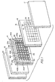
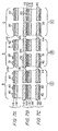
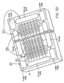
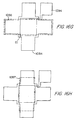
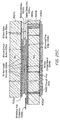
- a preferred embodiment of the invention for fabricating complex hybrid multi-function circuitry on common module substrates is illustrated in the context of an AMLCD, as shown in Fig. 1.
- the basic components of the AMLCD comprise a light source 10, such as a flat fluorescent or incandescent white lamp, or an electroluminescent lamp having white, or red, blue and green phosphors, a first polarizing filter 12, a circuit panel 14, an optional filter plate 16 and a second polarizing filter 17, which form a layered structure.
- Filter plate 16 is not needed for a black and white display or where the red, green and blue colors are provided by the lamp at the appropriate pixel.
- a liquid crystal material 23, such as a twisted nematic is placed between the circuit panel 14 and the filter plate 16.
- Circuit panel 14 consists of a transparent common module body 13 formed, for example, of glass upon which is transferred a plurality of common multifunction circuits comprising control logic circuits 40A and 40B and drive circuits 18A and 18B, 20A and 20B, and array circuit 25A and 25B.
- control logic circuits 40A and 40B and drive circuits 18A and 18B, 20A and 20B, and array circuit 25A and 25B are formed in tiles of x-Si.
- the array circuits may be formed in ⁇ -Si material, or poly-Si, or preferably in x-Si, to achieve lower leakage in the resultant TFT's and, hence, better grey scale. Higher speed is also achieved in x-Si.
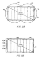
- a 4 x 8 inch active matrix LCD array can be formed from two standard 6-inch diameter Si wafers W1 and W2 as shown in Fig. 2A.
- Array circuit 25A is formed on wafer W1 and 1-inch by 4-inch tiles TA are transferred from the wafer W1 to the substrate 14. Note: The transfer may be accomplished using either a single or double transfer process, as will be described in detail below. Each tile is registered against another using micropositioning equipment and manipulators capable of micron scale accuracy. Similarly, tiles TB are transferred from wafer W2 to form array 25B on substrate or common module body 13 (See Fig. 2B).
- Logic circuits 40A and 40B and drive circuits 18A, 18B, 20A, 20B are formed on other suitable substrates (not shown) and tiled and transferred in like manner to common substrate 13 and registered opposite the arrays 25A, 25B, as shown in Fig. 1.
- conductive interconnections 50 are then made between the drive circuits and the individual pixels 22 and the logic control circuits 40A and 40B.
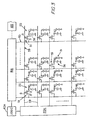
- a 1280 by 1024 addressable array of pixels 22 are formed on the substrate 13 of circuit panel 14.
- Each pixel 22 is actuated by voltage from a respective drive circuit 18A or B on the X-axis and 20A or B on the Y-axis.
- the X and Y drive circuits are controlled by signals from control logic circuits 40A and B.
- Each pixel 19 produces an electric field in the liquid crystal material 23 disposed between the pixel and a counterelectrode (not shown) formed on the back side of the color filter plate 16.
- the electric field formed by pixels 22 causes a rotation of the polarization of light being transmitted across the liquid crystal material that results in an adjacent color filter element being illuminated.
- the color filters of filter plate system 16 are arranged into groups of four filter elements, such as blue 24, green 31, red 27, and white 29.
- the pixels associated with filter elements can be selectively actuated to provide any desired color for that pixel group.
- Drive circuit 18A receives an including signal from control logic 40A and sends a signal to each source electrode of a TFT 51 in one of the columns selected by logic circuit 40A through interconnect line 53.
- Y-drive circuit 20A controlled by logic circuit 40A energizes a row buss 59 extending perpendicular to column buss 53 and applies a voltage pulse to each gate G of TFT's 51 in a selected row.
- a TFT has a voltage pulse on both its gate and source electrode current flows through an individual transistor 51, which charges capacitor 56 in a respective pixel 22.
- the capacitor 56 sustains a charge on the pixel electrode adjacent to the liquid crystal material (shown schematically at 19) until the next scan of the pixel array 25.
- the various embodiments of the invention may, or may not, utilize capacitors 56 with each pixel depending upon the type of display desired.
- the array circuits 25A and 25B and logic 40A,40B and drive circuits 18A,18B may be formed and transferred by a number of processes.
- the basic steps in a single transfer process are: forming of a plurality of thin film Si circuits on Si substrates, dicing the thin film to form tiles, and transferring the tiles to a common module substrate by "tiling.” Tiling involves the steps of transferring, registering the transferred tiles, and adhering the registered tiles. The Si substrates are then removed and the circuits on the tiles are interconnected.
- the double transfer approach described in detail below in connection with Figs. 4A-4L is similar except that the Si-substrate is removed after dicing and the thin film is transferred to an intermediate transfer body or carrier before ultimate transfer to the common module body.
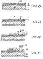
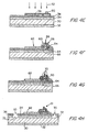
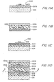
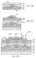
- the first step is to form a thin-film precursor structure of silicon-on-insulator (SOI) film.
- SOI structure such as that shown in Fig. 4A, includes a substrate 32 of Si, a buffer layer 30, of semi-insulating Si and an oxide 34 (such as, for example, SiO 2 ) that is grown or deposited on buffer layer 30, usually by Chemical Vapor Deposition (CVD).
- An optional release layer 36 of material which etches slower than the underlying oxide layer 34 is then formed over the oxide 34.
- a silicon oxy-nitride release layer comprising a mixture of silicon nitride (S 3 N 4 ) and silicon dioxide (SiO 2 ) may be a suitable choice.
- Such a layer etches more slowly in hydrofluoric acid than does SiO 2 alone. This etch rate can be controlled by adjusting the ratio of N and O in the silicon oxy-nitride (SiO x N y ) compound.
- a thin essentially single crystal layer 38 of silicon is then formed over the release layer 36.
- the oxide (or insulator) 34 is thus buried beneath the Si surface layer.
- the top layer is essentially single-crystal recrystallized silicon, from which CMOS circuits can be fabricated.
- the term "essentially" single crystal means a film in which a majority of crystals show a common crystalline orientation and extend over a cross-sectional area in a plane of the film for at least 0.1 cm 2 , and preferably, in the range of 0.5 - 1.0 cm 2 , or more.
- the term also includes completely single crystal Si.
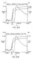
- a buried insulator provides devices having higher speeds than can be obtained in conventional bulk (Czochralski) material. Circuits containing in excess of 1.5 million CMOS transistors have been successfully fabricated in ISE material. An optional capping layer (not shown) also of silicon nitride may also be formed over layer 36 and removed when active devices are formed.
- the film 38 is patterned to define active circuits, such as a TFT's in region 37 and a pixel electrode region at 39 for each display pixel.
- active circuits such as a TFT's in region 37 and a pixel electrode region at 39 for each display pixel.
- TFT 51 and one pixel electrode 62 are illustrated (Fig. 4H). It should be understood that an array of 1280 by 1024 such elements can in practice be formed on a single 6-inch wafer.
- a plurality of arrays may be formed on a single six-inch wafer, which are then applied to the display as tiles and interconnected.
- the plurality of pixel matrices from one wafer can be separated and used in different displays.
- the plurality may comprise one large rectangular array surrounded by several smaller arrays (to be used in smaller displays). By mixing rectangular arrays of different areas, such an arrangement makes better use of the total available area on a round wafer.
- An oxide layer 40 is then formed over the patterned regions including an insulator region 48 formed between the two regions 37, 39 of each pixel.
- the intrinsic crystallized material 38 is then implanted 44 (at Fig. 4C) with boron or other p-type dopants to provide a n-channel device (or alternatively, an n-type dopant for a p-channel device).
- a polycrystalline silicon layer 42 is then deposited over the pixel and the layer 42 is then implanted 46, through a mask as seen in Fig. 4D, with an n-type dopant to lower the resistivity of the layer 42 to be used as the gate of the TFT.
- the polysilicon 42 is patterned to form a gate 50, as seen in Fig. 4E, which is followed by a large implant 52 of boron to provide p+ source and drain regions 66, 64 for the TFT on either side of the gate electrode.
- an oxide 54 is formed over the transistor and openings 60, 56, 58 are formed through the oxide 54 to contact the source 66, the drain 64, and the gate 50.
- a patterned metallization 71 of aluminum, tungsten or other suitable metal is used to connect the exposed pixel electrode 62 to the source 66 (or drain), and to connect the gate and drain to other circuit panel components.
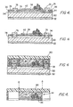
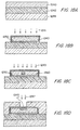
- the next step in the process is to transfer the silicon pixel circuit film to a common module, either directly, or by a double transfer from substrate to carrier and then to the common module.
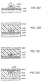
- a double transfer approach is illustrated in Figs. 4H-4L.
- a first opening 70 (in Fig. 4H) is etched in an exposed region of release layer 36 that occurs between tiles.
- Oxide layer 34 etches more rapidly in HF than nitride layer 36, thus a larger portion of layer 34 is removed to form cavity 72. A portion of layer 36 thus extends over the cavity 72.
- a support post 76 of oxide is formed to fill cavity 72 and opening 70, which extends over a portion of layer 36. Openings or via holes 74 are then provided through layer 36 such that an etchant can be introduced through holes 74, or through openings 78 etched beneath the release layer 36, to remove layer 34 (See Fig. 4J). The remaining release layer 36 and the circuitry supported thereon is now held in place relative to substrate 32 and buffer 30 with support posts 76.
- an epoxy 84 that can be cured with ultraviolet light is used to attach an optically transmissive superstrate 80 to the circuitry, and layer 36.
- the buffer 30 and substrate 32 is then patterned and selectively exposed to light such that regions of epoxy 84' about the posts 76 remain uncured while the remaining epoxy 84' is cured (See Fig. 4K).
- the buffer 30 and substrate 32 and posts 76 are removed by cleavage of the oxide post and dissolution of the uncured 84 epoxy to provide the thin film tile structure 141, shown in Fig. 4L mounted on carrier 80.
- the edges of the carrier 80 are trimmed to coincide with the tile borders.
- the nitride release layer 36 is removed by etching.
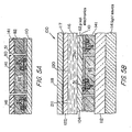
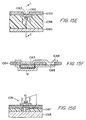
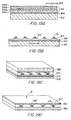
- a plurality of tile structures 141 are then sequentially registered with one another and adhered to a common module body 110 using a suitable adhesive (not shown).
- Common module body 110 is preferably patterned with interconnect metallization on the surface facing the tile structure 141 for interconnecting individual tile circuitry with each other.
- insulation and alignment layers, spacers, a sealing border and bonding pads for connections are bonded onto the periphery of the common module body 110.
- a screen printing process can be used to prepare the border. As shown in Fig.
- a plate 117 containing the color filters 120 and the counterelectrode (not shown) is bonded to the periphery thin film circuit tiles 141 with the sealing border after insertion of spacers (not shown).
- the display is filled with the selected liquid crystal material 116 via a small filling hole or holes extending through the border. This filling hole is then sealed with a resin or epoxy.
- First and second polarizer films 118, 112 or layers are then bonded to both sides and connectors (not shown) are added.
- a white light source 114, or other suitable light source is bonded to polarizer 112.
- Pixel electrodes 62 are laterally spaced from each other. Each pixel has a transistor 51 and a color filter 120 or 122 associated therewith.
- a bonding element or adhesive 82 and optically transmissive superstrate 110, such as glass or plastic completes the structure.
- Body 110 is preferably a low temperature glass that can have a thickness preferably of about 200 to 1000 microns.
- thin single-crystal films are grown by chemical vapor deposition (CVD), and separated from a reusable homoepitaxial substrate.
- the films removed from the substrate by CLEFT are "essentially" single-crystal, of low defect density, are only a few microns thick, and consequently, circuit panels formed by this process have little weight and good light transmission characteristics.
- the CLEFT process illustrated in U.S. Patent No. 4,727,047, involves the following steps: growth of the desired thin film over a release layer (a plane of weakness), formation of metallization and other coatings, formation of a bond between the film and a second substrate, such as glass (or superstrate), and separation along the built-in-plane of weakness by cleaving.
- the substrate is then available for reuse.
- the CLEFT process is used to form sheets of essentially single crystal material using lateral epitaxial growth to form a continuous film on top of a release layer.
- the lateral epitaxy is accomplished either by selective CVD or, preferably, the ISE process or other recrystallization procedures.
- other standard deposition techniques can be used to form the necessary thin film of essentially single crystal material.
- the release layer can comprise multi-layer films of Si 3 N 4 and SiO 2 .
- Such an approach permits the SiO 2 to be used to passivate the back of the CMOS logic.
- the Si 3 N 4 is the layer that is dissolved to produce the plane of weakness.
- the circuits are first bonded to the glass, or other transfer substrate, and then separated, resulting in simpler handling as compared to, for example, UV-cured tape.
- the plane of weakness is key to obtaining uniform cleaving between the circuits and the substrate.
- This plane may be formed by creating a pattern of carbon on the surface of the wafer so that only a small fraction of the underlying semiconductor surface is exposed. These exposed portions are used as nucleation cites for the epitaxial film. If the growth conditions are properly chosen, the film will grow laterally faster than vertically, leading to laterial overgrowth of the single crystal film. Within 1Im of vertical growth, the film becomes continuous and of high quality. However, the carbon layer is weak and, combined with the small fraction of exposed semiconductor areas where the film is strongly attached to the substrate, creates a plane of weakness. This plane can be used reliabily and reproducibly to separate the film from the substrate. The substrate may be reused. These processes have been used to transfer a wide range of GaAs and Si circuits to alternative substrates such as glass, ceramic, and other materials, without harm to the active circuitry.
- the oxide film is strongly attached to the substrate and to the top Si film which will contain the circuits. For this reason, it is necessary to reduce the strength of the bond chemically. This requires use of a release layer that is preferentially dissolved with an etchant without complete separation to form a plane of weakness in the release layer. The films can then be separated mechanically after the glass is bonded to the circuits and electrodes.
- Mechanical separation may be accomplished by bonding the upper surface of the Si film to a superstrate, such as glass, using a transparent epoxy.
- the film and glass are then bonded with wax to glass plates about 5 mm thick that serve as cleaving supports.
- a metal wedge is inserted between the two glass plates to force the surfaces apart. Since the mask has low adhesion to the substrate, the film is cleaved from the substrate but remains mounted on the glass.
- the substrate can then be used for another cycle of the CLEFT process, and the device processing may then be completed on the back surface of the film. Note that since the device remains attached to a superstrate, the back side can be subjected to standard wafer processing, including photolithography.
- One embodiment of the invention utilizes a recrystallization system, shown schematically in Fig. 6 to form the essentially single crystal Si thin film.
- a sample wafer 134 is formed of poly Si, formed on SiO 2 , formed on an Si wafer.
- a capping layer 138 is formed over the poly Si.
- the wafer temperature is then elevated to near the melting point by a lower heater 130.
- An upper wire or graphite strip heater 132 is then scanned across the top of the sample 134 to cause a moving melt zone 136 to recrystallize or further crystallize the polycrystalline silicon.
- the lateral epitaxy is seeded from small openings formed through the lower oxide.
- the resultant single crystal film has the orientation of the substrate.
- Figs. 7A-7D illustrate an alternate preferred double transfer process for adhering and transferring tiles of circuits of thin films of silicon to a common module body.
- the starting structure is a silicon wafer 118 upon which an oxide layer 116 and a thin film of poly-Si, A-Si or x-Si 114 is formed using any of the previously described processes such as ISE or CLEFT.
- a plurality of circuits, such as pixel electrodes, TFT's, Si drivers and Si logic circuits, are then formed in the thin film.
- Fig. 7A shows three such wafers, I, II, III. In wafer I, logic circuits 40 are formed. In wafer II, pixel electrodes 62 and TFT's 51 are formed.
- driver circuits 20 are formed.
- a wafer, or individual tiles diced from the wafer, is attached to a superstrate transfer body 112, such as glass or other transparent insulator, using an adhesive 120.
- the adhesive is comprised of commercially available epoxies.
- the wafer, or tile, is then cleaned and the native oxide 118 is etched off the back surface. Depending on the thickness of the wafer, it may take up to 5 hours to etch the Si 118 and oxide 116 layers.
- the solution etches silicon very rapidly, i.e. 2 to 3 microns/min., and uniformly if the wafers are held horizontally in the solution with the etching surface face up.
- the acid has a very low etch rate on oxide, so that as the substrate is etched away and the buried oxide is exposed, the etching rate goes down. The observer can monitor the process and to stop the etch in the buried oxide layer 116' without punching through to the thin silicon layer 114 above it.
- Wafers up to 25 mils thick and oxides as thin as 4000 ⁇ have been successfully etched using this process.
- An alternative etchant is hydrazine, which has a much higher etch rate selectivity or ethylene diamine pyrocatacol (EDP).
- the thin films 114 transferred to the respective glass superstrates 112 are now rinsed and dried. If not already provided with circuits 40, 51, 62 or 20, the films 114 can be backside circuit processed, if desired.
- transfer bodies 112 After all the necessary circuits are formed, as above, on transfer bodies 112, they may now be diced and tiled onto a common module body 13 (Fig. 7D) to perform a combined function, such as an AMLCD.
- the logic circuits 40 of transfer body 118 in col. A, Fig. 7C, are transferred to the border of module body 13, while the driver circuits 20 from the transfer body 118 in col. C, Fig. 7C, are disposed on the border between the logic circuits 40A and 40B.
- Tiles of pixel electrodes 62 and TFT's 51 are formed by dicing or etching and are registered with respect to each other and pre-formed wiring 50 on module body 13, as shown.
- the transfer body 118 and the epoxy 120 is removed using a suitable etchant, such as HF for the case of a glass transfer body.
- the film can be transferred to another substrate and the first glass superstrate and adhesive can be etched off, allowing access to the front side of the wafer for further circuit processing.
- Figs. 8A and 8B illustrate an alternative one-step silicon thin film transfer process in which GeSi is used as an intermediate etch stop layer.
- Si buffer layer 126 is formed on an x-Si substrate 128 followed by a thin GeSi layer 129 and a thin A-Si, poly-Si, or x-Si device or circuit layer 132; using well-known CVD or MBE growth systems.
- the layer 132 is then IC processed in the manner previously described in connection with Figs. 4E-H, to form circuits, such as TFT's 200 and pixel electrodes 202 (Fig. 8A).
- the processed wafers, or tiles from the wafer are mounted on a common module glass (or other) support 280 using an epoxy adhesive of the type previously mentioned in connection with Figs. 7A-7B.
- the epoxy fills in the voids formed by the previous processing and adheres the front face to the superstrate 280.
- the original Si substrate 128 and Si buffer 126 are removed by etching, which does not affect the GeSi layer 129 (Figs. 8B).
- the GeSi layer 124 is removed by brief submersion in a suitable etch.
- Figs. 9A-9B illustrate an alternate embodiment related to isolating and transferring circuits.
- a method of fabricating pressure sensing transducers on a glass substrate is shown in Figs. 9A-9B and described hereinafter.
- the transducer circuit operates by sensing a change in the resistance of the p-region 904 in response to pressure applied to the circuit. This resistance change may be sensed by an ohmmeter coupled across contacts 912 and 912 and calibrated and converted into a pressure sensor to serve as a strain gauge.
- the starting structure is shown in Fig. 9A.
- An SOI wafer which consists of an Si substrate 900 beneath a buried oxide layer 902, upon which is formed a single, or nearly single, crystal Si layer 904.
- a blanket implant of boron ions is made to make the Si layer a p-type conductor.
- a thin (1000 ⁇ ) blanket protective/mask layer of oxide (SiO 2 ) (not shown) is then formed over the structure. (Note Fig. 9A shows the structure after processing).
- Single, or nearly single, islands of x-Si are then formed by applying photo-resist over the oxide structure and etching the oxide and silicon 904 between islands to align the edges of the islands parallel to the [110] plane.
- Photo resist is applied again and contact openings formed to contact regions 910 and 908, which are then implanted with a high dose of boron ions to form P + type conductivity regions.
- a protective oxide layer 906 is then formed over the island.
- Aluminum contact pads, 912 and 913 to the contacts 908, 910 are formed in openings provided through oxide 906.
- the pressure transducer circuit of Fig. 9A is now ready for transfer to a temporary glass substrate.
- the circuit is transferred to a temporary substrate 920 using a removable epoxy 922.
- the silicon substrate 900 is etched away.
- the initial oxide layer 902 is etched around the periphery of the circuit 918 leaving the circuit free to be inverted and transferred to the glass substrate 920 and releasibly bonded thereto.
- Figs. 10A and 10B illustrate an alternate transfer process in which the initial oxide 902 is etched about the periphery of each circuit 918 using a conventional photo-resist and mask technique.
- the Si substrate 900 is also etched locally which preferentially etches Si to reveal the [111] plane.
- a nitride layer may be added such that the etchant does not etch the aluminum. Etching of the Si substrate with hydrazine undercuts the circuits 918 forming a cavity 930 under the circuits and leaving a bridge structure 934 between circuits 918 and the substrate.
- a vacuum wand may be used to seize one or more circuits and break the bridge to remove the circuits which may then be transferred along with other circuits to a common module substrate and aligned and interconnected with other circuitry to perform an overall function as previously described.
- other techniques such as laser ablation can be used for removing the circuits from the substrate.
- Fig. 10B is a top-plan view of Fig. 10A before substrate 900 is etched where the bridges 934 are shown.
- the bridges make an angle of about 22 1 / 2 relative to the long symmetry axis of the circuit 918.
- a first circuit 1000 (Fig. 11A) formed in a silicon layer 1002 on an oxide layer 1004 on an Si substrate 1001 is transferred onto a glass superstrate 1006 as shown in Fig. 11B. More specifically, the single-transferred circuit 1000 is transferred to a glass superstrate, coated with amorphous silicon, by any of the aforementioned transfer methods and bonded to the glass with an adhesive or epoxy 1008.
- a second circuit 1010 is double-transferred to a glass or diamond substrate 1011.
- the circuit 1010 is preferably formed in a layer of silicon 1012 on an oxide layer 1014, and is bonded to the substrate by a layer of adhesive or epoxy 1016.
- a three-dimensional device is formed by bonding the single-transferred circuit 1000 (Fig. 11B) on top of the double-transferred circuit 1010 (Fig. 11C) using thin, uniform adhesive 1018. Since the circuits can be observed through the glass substrate 1011, they can be aligned using a microscope or a contact or proximity aligner as routinely done in photolithography where a mask is aligned on top of a silicon circuit in process or by other appropriate micropositioning tools or techniques.
- the superstrate 1006 is removed as in a double-transfer process and the adhesive 1008 is removed in oxygen plasma. This leaves the front surface of the top circuit 1000 exposed.
- the bottom circuit 1010 is buried beneath the adhesive layer 1018.
- openings or via holes are defined by appropriate etchants in order to expose contact areas on the two circuit layers. All of the oxide is etched in buffered HF using photoresist as a mask while the adhesive can be etched in oxygen plasma or by reactive ion etching (RIE) using the previously etched oxide as a mask.
- RIE reactive ion etching
- Figs. 12A-12B show performance curves of a lower MOSFET circuit of a three-dimensional device (such as in Fig. 11D) and the corresponding curves for a similar device after double-transfer and before three-dimensional mounting (such as in Fig. 11C).
- the graphs of Figs. 12A-12B show that the transconductance and the drive current are higher when the circuit is buried under epoxy (Fig. 11D) than when it is exposed to ambient air (Fig. 11C). This effect can be explained by a higher thermal conductivity of the epoxy with respect to air which results in a reduced heating effect for the circuit buried in epoxy (Fig.
- An advantage of this approach is the capability to integrate heat sink layers within the stack. Heat dissipation is an important problem in 3D architectures, and a capability for insertion of heat conducting layers between active electronic layers is advantageous. These layers can have much higher thermal conductivity than can be attained in Si or other semiconductors that may be envisioned for heat transfer.
- Fig. 13A is a sectional view of Fig. 11D taken along the line A-A and shows the lower contact area 1020 formed via metalization in the plane of the silicon layer 1012 for providing electrical connection to the circuit 1010 (Fig. 11D).
- upper contact areas are formed directly above the lower areas in the plane of the silicon layer 1002 and are electrically connected to the upper circuit 1000 (Fig. 11D).
- the upper and lower areas (1024, 1020) employ an optional poly-Si layer for strengthening the areas for contacts.
- Via holes 1022 are formed through the upper contact areas 1024 to gain access to the lower contact areas 1020.
- the etching to form the via holes with high aspect ratio is performed by an RIE technique.
- Electrical contact between the upper and lower devices is made by filling the via holes 1022 with an electrically conductive material such as tungsten or aluminum.
- ground planes 1026 are positioned between device layers 1028 and 1030 to prevent electrical interference.
- These conductive ground planes 1026 can be made with a metal or by ITO deposition on the surface of the oxide layer 1032 opposite the device 1034.
- the ground planes can be formed with an electrically conductive epoxy or with a highly doped silicon layer taking the place of a device layer in the stacked structure.
- a benefit of using transfer technology to form a multilayer stack is attained if superior radiation resistance and low weight are desired.
- the removal of the substrate decreases the probability of single event upset and reduces the weight, but also important is the potential for utilization of high-Z radiation shielding material at the outside surfaces of the device. This shielding can protect many layers of stacked circuits with much less increase in weight than is needed for a 2D geometry. Thus, there are important benefits for space applications in which radiation resistance and weight are important factors.
- a further benefit of the proposed technology is that the multi-layer circuit may be made tamper resistant. This benefit is particularly important for the prevention of reverse engineering for proprietary circuits.
- the die In a 2D circuit, the die can be removed from the package and examined by microanalytic techiques.
- a 3D circuit can be formed in such a way that separation of the layers is not only difficult, but also highly destructive, so that separation of the layers would not yield meaningful patterns or useful reverse-engineered data.
- Speed advantages can be attained by using a 3D approach. For example, in a memory comprising stacked 2D circuits access time can be reduced because the transit distance for address signals is shorter than a comparable tilted planar 2D memory. As another example by using a 3D addressing scheme for a true 3D architecture, access time may be reduced to an even lower level.
- Transfer of circuits into a 3D architecture can also permit the integration of high speed GaAs analog signal processing circuitry (MMICs) with silicon circuits. This permits the integration of microwave circuits with high speed highly dense Si circuits. Such versatility may not be easy to obtain with other approaches. Transfer is also applicable to digital GaAs circuitry.
- MMICs analog signal processing circuitry
- a fabrication process comprising single and double transfer steps and a backside processing step can be employed to provide various 3-D devices.
- the fabrication process includes the formation of circuits in a Si film of an SOI structure, adhering the circuits to a superstrate and removal of the substrate. At this point, the silicon circuits have been single-transferred and the backside of the silicon circuit layer is exposed. Backside processing can be performed so long as the processing is compatible with the selected adhesive. After backside processing is performed, the silicon circuit layer is transferred to a glass substrate (double-transfer).
- a double gate MOSFET can be formed in accordance with the above-described fabrication process.
- a standard MOSFET device 1050 having a drain (D), a gate (G1) and a source (S) (Fig. 15A) is formed by an suitable method such as described previously herein.
- the next step in the process is to transfer the device film 1052 from its substrate 1056 to a superstrate for backside processing.
- a single transfer approach is shown in Figs. 15B-15D.
- an epoxy 1058 is used to attach an optically transmissive superstrate 1060.
- a glass superstrate coated with A-Si is employed with a two-part epoxy.
- the substrate 1056 is etched. As shown in Fig. 15C, the etchant rapidly removes the silicon substrate 1056 with the oxide layer 1054 serving as an etch stop.
- the etch rate selectivity of 200:1 for silicon versus thermal silicon dioxide allows the use of very thin oxide layers leaving the device 1050 protected from the etchant.
- the oxide layer 1054 is thinned down to a few hundred angstroms ( ⁇ 500) along the channel region 1062 (Fig. 15D).
- a thin oxide layer adjacent the backside of the MOSFET device 1050 is illustrated in Fig. 15E.
- the oxide layer along the channel region 1062 is etched away to expose the backside of the device 1050.
- a thin oxide layer 1063 ( ⁇ 500 ) can be deposited in the region 1062.
- a second gate (G2) is then formed over the thin oxide layer 1063 and electrically connected to the first gate (G1) as follows.
- Fig. 15F which is a cross-sectional view of the structure shown Fig. 15E a contact hole 1065 can be opened through the thinned oxide, and a gate material (1066) can be deposited and etched to form a second gate (G2) 1064 which is electrically connected to the first gate (G1).
- This dual gate configuration serves to practically double the drive current for the MOSFET 1051 since the device has two channels.
- the dual gate MOSFET 1051 may be transferred again and bonded with epoxy 1067 to a permanent substrate 1068 such as glass.
- a 3-D double-gate MOSFET inverter 1070 can be fabricated such that the n-channel and p-channel MOSFETS share the same body with their channels disposed on opposite sides thereof.
- the fabrication sequence for providing a double-gate inverter is shown in Figs. 16A-16J.
- the device 1070 includes an n-channel MOSFET 1072 with a gate (G1), source (S1) and drain (D1) and a p-channel MOSFET 1074 with a gate (G2), source (S2) and a drain (D2).
- the shared region 1076 includes the n-channel 1078 and the p-channel 1080 which are disposed on opposite sides of the region. More specifically, the channel for the n-channel MOSFET is disposed along the top interface 1081 of the shared region and the channel for the p-channel MOSFET is disposed along the bottom interface 1082 of the shared region.
- FIG. 16C illustrates the channel doping for the p-channel MOSFET.
- a photoresist and a mask are positioned over the patterned silicon island 1084 and phosphorous (or other n-type dopants) is implanted into the area 1086 with a projected range (R p ) near the bottom interface 1082 (Fig. 16B).
- the implant is such that the phosphorous concentration at the bottom interface is about 10 16 cm -3 .
- Fig. 16D illustrates the channel doping for the n-channel MOSFET.
- boron (or other p-type dopants) is implanted in the area 1088 with an R p near the top interface 1081 (Fig. 16B).
- the implant preferably produces a boron concentration at the top interface of about 4 x 10 16 cm -3 .
- Fig. 16E illustrates the formation of the channel stop 1083 (Fig. 16B) for the n-channel MOSFET.
- a photoresist and mask are positioned over the silicon island such that boron is implanted into the regions 1089 with an R p in the in the middle of silicon. This implant is such that the average boron concentration in the middle of the silicon is about 4 x 10 16 cm -3 .
- Fig. 16F illustrates an edge implant for the n-channel MOSFET.
- the corner regions 1077 (Fig. 16A) extend beyond the gate material preventing the gate from contacting the sidewall of the silicon island to form a sidewall transistor.
- corner regions are heavily doped to minimize sidewall transistor effects on the double-gate inverter.
- boron or other p-type dopant is implanted into the areas 1090 with an R p near the top interface.
- the implant preferably produces a boron concentration at the top interface of about 5 x 10 17 cm -3 .
- the gate (G1) and the contact area 1094 are then formed for n-channel MOSFET.
- the source/drain doping is performed for the n-channel device.
- arsenic or other n-type dopants
- Fig. 16H illustrates the formation of the channel stop 1079 (Fig. 16B) for the p-channel MOSFET.
- phosphorus or other n-type dopants
- G1 phosphorus
- Fig. 16B the gate
- boron is implanted into the areas 1098 with a R p in the middle of the silicon and an average boron concentration of 10 20 cm -3 .
- the gate (G2) is formed for the p-channel MOSFET and electrically connected to the gate (G1).
- Fig. 16J which is a sectional view of Fig. 16A taken along the line J-J
- the double-gate MOSFET is single transferred to a temporary superstrate 1100 and attached to the superstrate by an adhesive or epoxy 1102.
- the oxide layer 1104 upon which the device is disposed is selectively etched using a photoresist and a mask to open two areas 1106 and 1108.
- the gate (G2) is formed in the area 1106 by metalization as well as the contact path 1110 to the contact area 1094. After metallization, the two gates are electrically connected.
- a three-dimensional inverter is formed with a pair of MOSFETs which are vertically stacked as shown in Fig. 17D.
- the fabrication process for the three-dimensional inverter is shown in Figs. 17A-17D.
- an n-channel device 1200 is formed in single crystal silicon 1202 on an oxide 1204 over a substrate (not shown). After a double transfer, the device 1200 is attached with an adhesive or epoxy 1208.
- a passivation oxide layer 1210 is deposited over the device 120.
- a p-channel device 1212 is separately fabricated in single crystal silicon 1214 on an oxide 1216 on a substrate (not shown).
- An oxide layer 1224 is deposited over the p-channel device 1212 for passivation, and single transfer is performed such that the device is attached to a superstrate 1218 by an adhesive 1220.
- the p-channel device 1212 is then attached to the n-channel device by an adhesive 1222 forming a stacked structure (Fig. 17C).
- an oxide layer 1224 is deposited over the p-channel device 1212 for passivation.
- vias 1226 are then formed to access the gate, source and drain regions of the upper device 1212 and the buried device 1200.
- a metal layer 1228 is deposited and patterned to form electrical interconnects, for the stacked inverter structure 1230. It is noted that the interconnection of the respective gates is made in a plane parallel to the figure such that the vias are not shown.
- a vertical bipolar transistor is fabricated in accordance with the principles of the present invention.
- the fabrication process sequence is shown in Figs. 18A-18H. Beginning with a silicon film 1240 on an oxide 1242 on a substrate 1244 (Fig. 18A), the silicon is patterned into device regions as shown in Fig. 18B. Next, a deep implant of an n-type dopant 1241 is performed for producing an n-doped collector region 1250. Referring to Fig. 18C, the device region is doped with boron or other p-type dopants 1243 for providing a p-type base region 1251. Referring to Fig.
- the silicon is doped with an n-type dopant 1244 to provide an n+ emitter region 1245.
- the silicon is heavily doped with an n-type material 1247 to provide an n+ collector region 1248 (Fig. 18E).
- the collector, emitter and base contacts 1252 can be formed (Fig. 18F) and the device can be transferred to a superstrate 1254 (Fig. 18G).
- the device is attached to the superstrate with an epoxy 1256 and inverted for further processing.
- a portion of the oxide layer 1242 is etched forming an opening 1258 at the back of the silicon layer.
- a metal layer 1260 is applied over the exposed backside of the silicon film and sintered (Fig. 18H).
- a high temperature implant (-450 1 / 2C) can be implemented prior to metalization to produce an n+ buried conductor layer 1250 provided that a high temperature epoxy is used.
- Three dimensional circuits can also be fabricated in III-V semiconductor materials, with appropriate release layer material and etchant.
- an AlGaAs/GaAs device an AlAs release layer is preferred.
- an InP device an InGaAs release layer is preferred.
- AlAs is preferentially etched by HF acid, while InGaAs is preferentially etched by sulfuric/hydrogen peroxide and water solution. The process can also be extended to II-VI semiconductor circuits.
- III-V circuit array in accordance with the invention, will be described with reference to Figs. 19A-D. It begins with the epitaxial growth of the required heteroepitaxial layers of AlGaAs and GaAs layers on a GaAs or Ge substrate.
- an optional layer 314 of AlAs is formed between the active AlGaAs layers 316 and the substrate 312 to facilitate substrate removal by the etch-off method.
- the AlAs forms an etch stop layer.
- the X-Y array can be removed from the substrate by a CLEFT process (See U.S. Patent No. 4,727,047 issued February 23, 1988 to Fan et al.) or chemical epitaxial lift-off.
- a layer of AlAs can be used as an etch stop, but AlAs is not really necessary, since the Ge substrate can be dissolved in H 2 O 2 without harm to the AlGaAs active layers.
- Fig 19A shows the epitaxial layer structure to comprise an active GaAs (or AlGaAs) layer 366 formed by OMCVD.
- a pattern of contact pads 119 and busbars (not shown) is formed by photolithographic techniques, evaporation, and/or electroplating on the front surface, as shown in Fig. 19B.
- the circuits 313 are isolated by etching part way into the epitaxial layers 316, as shown in Fig. 19B. This step is not absolutely required at this point, however, it simplifies a later etch step in the process.
- the next stage of the process consists of bonding of the wafer to a support 380, such as glass, ceramic, or thin stainless steel. If the support is transparent to infrared radiation, downstream front-to-back alignments are facilitated, but the alignments can also be carried out by careful registration to the support edges.
- the processed front side is bonded to the support 380 using a suitable adhesive (not shown) (Fig. 19C).
- a suitable adhesive not shown
- the wafer or substrate 312 is etched off (or cleaved off) leaving the thin film 316 attached to the support 380, as shown in Fig. 19D, in which the structure has been flipped over onto the support to expose the backside B for processing.
- any remaining non-essential material is removed from the back by selective etching in HF to expose a clean GaAs contact layer B.
- the backside contacts 321 and busbars 321x are now photolithographically patterned and electroplated or evaporated onto the contact regions 316'.
- the front backside processed circuit array 330 may be mounted directly to a silicon wafer 323 in a precise location 310 with X and Y silicon driver circuits 320 and 322 formed in wafer 323 and coupled to the X and Y bonding pads 324 and 326, respectively. Bonding of array 330 to wafer 323 may also be accomplished by having the contact pads 326 replaced by cantilevered bars that extend over to pads on wafer 323 and which can be trimmed to form circuit bonding pads.
- undesired epitaxial layers are removed; these layers are present to initiate the epitaxy, or may be buffer layers that are not needed in the final device.
- AlAs etch stop layer may be provided in the epitaxy between these layers and the epitaxial device structure.
- the layers can then be removed in etches that stop at AlAs, such at the well known PA etches. At a pH of about 8, these etches dissolve GaAs 1000 times faster than AsGaAs.
- the AlAs can be removed in HF or HCl.
- the backside of the substrate is provided with multiplex-compatible metallization to contact the back of each pixel. Note that this type of processing requires front-to-back alignment.
- the pixels are then separated by a mesa etch. Because the films are only about 5 microns thick, the mesa etch is straightforward and quick.
- the etching may be accomplished with either wet or dry processing. At this point, the exposed semiconductor may be coated with dielectric to prevent association.
- a detector 450 and LED array 300 can be stacked into a hybrid assembly comprised of a top thin film IR X-Y detector array 450 affixed by light transparent glue to lower thin film LED array 300 mounted on glass substrate 620.
- a glass lens 460 is affixed to the top surface of detector 450 and heat transfer openings 460 provided as necessary for cooling purposes.
- the entire structure can be quite thin (1 mil), with the electronics 470 provided around the periphery.
- the monolithic thin film array can be mounted on ordinary glasses for image enhancement of visible light, as well as for display of data superimposed on video images.
- the applications of the device of Fig. 21 include military night vision systems, range finders, advanced military avionics, personal communications systems, and medical systems in which real-time image enhancement is useful.
- X-Y arrays can also be used to form a multicolor display.
- individual X-Y arrays labelled LED1, LED2 and LED3, are formed from two or more different epitaxial structure.
- the primary difference in the structure is in the active layer material 161, 162 and 163, which must have different band gaps to create different colors.
- red 163 can be created with AlGaAs
- green 162 can be created with InAsGaP.
- the top device LED1 may be a blue LED formed of II-VI material, such as ZnSe, ZnSSe or a group IV alloy such as SiC.
- the arrays must be stacked with the larger bandgap LED1 closer to the observer.
- the material with the larger bandgap will be transparent to the radiation from the smaller bandgap. Thus, in this way, the observer will be able to see both colors.
- the creation of the stack of three LEDs 1020 is as follows: first, the three separate LED arrays LED1, LED2 and LED3 are formed, as previously described. Next, they are stacked together with glass 600 between them.
- Transparent glue or epoxy 400 is used to bond the stacks on top of each other.
- the upper and lower bonding pads P1 and P2 on each LED are laterally staggered with respect to other LEDs, so that individual LED pixels may be addressed (See plan view Fig. 23).
- Integrated circuits fabricated on other materials can also be stacked into 3D circuit modules using a transfer process as described above.
- the circuits can be fabricated in II-VI or I-VIII compounds or in diamond thin films.
- a 3D circuit module may comprise stacked layers of differing materials.
- GaAs circuits can be stacked adjacent to Si circuits
- Fig. 24A illustrates a 3D circuit stack interconnected by conductive material.
- the circuits layers 1410, 1410', 1410'' are stacked onto a carrier substrate 1401.
- the circuit layers 1410, 1410', 1410'' are fabricated separatedly using an above-described transfer process.
- the circuit layers 1410, 1410', 1410'' are adhered to the carrier substrate 1401 and to adjacent circuit layers by interleaved thin-film epoxy layers 1420, 1420', 1420''.
- interconnects 1414 are formed by patterning and etching the epoxy layers 1420', 1420'' to form vias and then depositing a thin-film metallization layer into the vias.
- the epoxy may be impregnated or supersaturated with a thermal conductive material, such as diamond.
- Fig. 24B is a schematic diagram of stacked circuit layers comprising contactless interconnects. Shown are two thin film circuit layers 1410, 1410'' interconnected within a thin film circuit module having a plurality of thin film circuit layers. Each interconnected circuit layer 1410, 1410'' comprises a contactless coupling element 1415, 1415' registered to each other. The plurality of circuit layers are transferred and adhered by interleaved epoxy layers 1420, 1420', 1420''.
- any intervening circuit layer 1410' must be patterned and etched to form vias through that layer.
- the intervening circuit layer 1410' is patterned and etched prior to transfer.
- the via 1435 is registered to the coupling elements 1415, 1415'.
- the vias 1435 are filled by epoxy.
- the intervening layer may also be coupled to the via 1435 by a coupling element (not shown) to create a chain of interconnected circuit layer.
- the contactless coupling elements 1415, 1415' are transferred LED and detector pairs.
- the electrical signals are encoded, optically transmitted to the respective circuit layer, where the optical signal is decoded.
- the receivers may be transferred patterned fine resolution photovoltaics.
- the epoxy 1420, 1420', 1420'' must be at least partially transmissive to wavelength of light being transmitted by the LED's.
- a single circuit layer 1410 may transmit to another particular layer within a chain at interconnected layers utilization of LEDs with various wavelengths chosen to match various detectors.
- the circuit layers 1410, 1410' are capacitive-coupled by the contactless coupling elements 1415, 1415'.
- the coupling elements 1415, 1415' are metallic plates and the epoxy layers 1420, 1425 are diamond impregnated to function as a dielectric separating the two plates.
- the circuit layers 1410, 1410' may be inductive-coupled, where the coupling elements 1415, 1415' are inductive loops.
- MMICs monolithic microwave integrated circuits
- thermally conductive layers can be inserted between stacked circuit layers to enhance heat transfer to an external heat sink. These layers can also increase the dielectric strength of the intercircuit insulators.
- the thermally conductive layers are fabricated as thin film layers.
- the thermally conductive layers may comprise thin film diamond, SiC, AlN, Aluminum, Zr, Ceramics or BeO. The choice of thermally conductive material is dependent on the engineering application.
- FIG 25A is a schematic diagram of a thin film module having thermally conductive layers.
- the stacked module has been transferred to a SiC carrier substrate 1510.
- the module comprises interleaved layers of thermally conductive material 1520a-m and circuit layers 1530a,m.
- the thin film circuit layers 1530a-m are interconnected by substrate vias 1535.
- FIG 25B is an exploded view of a section of the stacked circuit module Figure 25A.
- the thermally conductive layers 1520 comprise Sic. Stripline flex connectors 1535b and 1525d function to dissipate themal energy from the thermally conductive layers 1520b and 1525d to a heat sink.
- the thin film circuitry 1530 is isolated from the thermally conductive layers 1520 by a diamond thin film dielectric layer 1542, 1544.
- the dielectric layer 1542, 1544 is a diamond inpregnated epoxy.
- the thickness of the dielectric layers 1542, 1544 is determined by the diamond grit diameter, which is preferably about 5 microns.
- FIG 25C is an exploded view of the thin film module layers of Figure 25B.
- the circuit layer interconnect system is detailed.
- an optical interconnect system is used.
- Fabricated in the circuit layers 1530 are GaAs emitters 1552 and detectors 1554. The emitters are driven by respective optical drivers 1551, 1553.
- the stacked thin film semiconductor layers described herein have thicknesses within the range of 0.1 micron to 10 microns and preferably between 0.25 micron and 1.0 micron.
- embodiments of the present invention may include the features of the following enumerated paragraphs ("paras").
Landscapes
- Physics & Mathematics (AREA)
- Engineering & Computer Science (AREA)
- General Physics & Mathematics (AREA)
- Nonlinear Science (AREA)
- Optics & Photonics (AREA)
- Chemical & Material Sciences (AREA)
- Crystallography & Structural Chemistry (AREA)
- Mathematical Physics (AREA)
- Health & Medical Sciences (AREA)
- Life Sciences & Earth Sciences (AREA)
- Microelectronics & Electronic Packaging (AREA)
- Computer Hardware Design (AREA)
- Theoretical Computer Science (AREA)
- Signal Processing (AREA)
- Multimedia (AREA)
- Biomedical Technology (AREA)
- Veterinary Medicine (AREA)
- Heart & Thoracic Surgery (AREA)
- Medical Informatics (AREA)
- Molecular Biology (AREA)
- Surgery (AREA)
- Animal Behavior & Ethology (AREA)
- General Health & Medical Sciences (AREA)
- Public Health (AREA)
- Ophthalmology & Optometry (AREA)
- Biophysics (AREA)
- Human Computer Interaction (AREA)
- Thin Film Transistor (AREA)
- Liquid Crystal (AREA)
- Design And Manufacture Of Integrated Circuits (AREA)
- Solid State Image Pick-Up Elements (AREA)
- Facsimile Heads (AREA)
Applications Claiming Priority (5)
| Application Number | Priority Date | Filing Date | Title |
|---|---|---|---|
| US07/834,849 US5258325A (en) | 1990-12-31 | 1992-02-13 | Method for manufacturing a semiconductor device using a circuit transfer film |
| US834849 | 1992-02-13 | ||
| US874588 | 1992-04-24 | ||
| US07/874,588 US5376561A (en) | 1990-12-31 | 1992-04-24 | High density electronic circuit modules |
| EP93905940A EP0626099B1 (fr) | 1992-02-13 | 1993-02-12 | Procede de fabrication d'un modul de circuits electroniques a haute densite |
Related Parent Applications (1)
| Application Number | Title | Priority Date | Filing Date |
|---|---|---|---|
| EP93905940A Division EP0626099B1 (fr) | 1992-02-13 | 1993-02-12 | Procede de fabrication d'un modul de circuits electroniques a haute densite |
Publications (1)
| Publication Number | Publication Date |
|---|---|
| EP1237191A2 true EP1237191A2 (fr) | 2002-09-04 |
Family
ID=27125740
Family Applications (2)
| Application Number | Title | Priority Date | Filing Date |
|---|---|---|---|
| EP02076327A Withdrawn EP1237191A2 (fr) | 1992-02-13 | 1993-02-12 | Modules de circuits électroniques à haute densité |
| EP93905940A Expired - Lifetime EP0626099B1 (fr) | 1992-02-13 | 1993-02-12 | Procede de fabrication d'un modul de circuits electroniques a haute densite |
Family Applications After (1)
| Application Number | Title | Priority Date | Filing Date |
|---|---|---|---|
| EP93905940A Expired - Lifetime EP0626099B1 (fr) | 1992-02-13 | 1993-02-12 | Procede de fabrication d'un modul de circuits electroniques a haute densite |
Country Status (7)
| Country | Link |
|---|---|
| US (3) | US5376561A (fr) |
| EP (2) | EP1237191A2 (fr) |
| JP (1) | JPH07504782A (fr) |
| AT (1) | ATE227887T1 (fr) |
| CA (1) | CA2129123A1 (fr) |
| DE (1) | DE69332482T2 (fr) |
| WO (1) | WO1993016491A1 (fr) |
Cited By (12)
| Publication number | Priority date | Publication date | Assignee | Title |
|---|---|---|---|---|
| US7755457B2 (en) | 2006-02-07 | 2010-07-13 | Harris Corporation | Stacked stripline circuits |
| US8134153B2 (en) | 2002-10-18 | 2012-03-13 | Semiconductor Energy Laboratory Co., Ltd. | Semiconductor apparatus and fabrication method of the same |
| US8344992B2 (en) | 2000-02-29 | 2013-01-01 | Semiconductor Energy Laboratory Co., Ltd. | Display device and method for fabricating the same |
| WO2013083819A1 (fr) * | 2011-12-07 | 2013-06-13 | Osram Gmbh | Agencement de diodes électroluminescentes |
| US8891280B2 (en) | 2012-10-12 | 2014-11-18 | Micron Technology, Inc. | Interconnection for memory electrodes |
| US9025398B2 (en) | 2012-10-12 | 2015-05-05 | Micron Technology, Inc. | Metallization scheme for integrated circuit |
| US9190144B2 (en) | 2012-10-12 | 2015-11-17 | Micron Technology, Inc. | Memory device architecture |
| US9224635B2 (en) | 2013-02-26 | 2015-12-29 | Micron Technology, Inc. | Connections for memory electrode lines |
| US9659524B2 (en) | 1999-06-21 | 2017-05-23 | Semiconductor Energy Laboratory Co., Ltd. | Light-emitting device including substrate having cavity, and method for fabricating the light-emitting device |
| US10074693B2 (en) | 2015-03-03 | 2018-09-11 | Micron Technology, Inc | Connections for memory electrode lines |
| US10325940B2 (en) | 2001-11-30 | 2019-06-18 | Semiconductor Energy Laboratory Co., Ltd. | Vehicle, display device and manufacturing method for a semiconductor device |
| US12200950B2 (en) | 2021-03-05 | 2025-01-14 | Semiconductor Energy Laboratory Co., Ltd. | Electronic device |
Families Citing this family (206)
| Publication number | Priority date | Publication date | Assignee | Title |
|---|---|---|---|---|
| US6143582A (en) * | 1990-12-31 | 2000-11-07 | Kopin Corporation | High density electronic circuit modules |
| CN100465742C (zh) | 1992-08-27 | 2009-03-04 | 株式会社半导体能源研究所 | 有源矩阵显示器 |
| US6608654B2 (en) | 1992-09-11 | 2003-08-19 | Kopin Corporation | Methods of fabricating active matrix pixel electrodes |
| US5705424A (en) * | 1992-09-11 | 1998-01-06 | Kopin Corporation | Process of fabricating active matrix pixel electrodes |
| EP1178530A2 (fr) * | 1993-09-30 | 2002-02-06 | Kopin Corporation | Processeur 3-dimensionel utilisant des circuits à couche mince transferé |
| US7081938B1 (en) | 1993-12-03 | 2006-07-25 | Semiconductor Energy Laboratory Co., Ltd. | Electro-optical device and method for manufacturing the same |
| US5473222A (en) * | 1994-07-05 | 1995-12-05 | Delco Electronics Corporation | Active matrix vacuum fluorescent display with microprocessor integration |
| DE4433833A1 (de) * | 1994-09-22 | 1996-03-28 | Fraunhofer Ges Forschung | Verfahren zur Herstellung einer dreidimensionalen integrierten Schaltung unter Erreichung hoher Systemausbeuten |
| JPH09509792A (ja) * | 1994-12-23 | 1997-09-30 | フィリップス エレクトロニクス ネムローゼ フェンノートシャップ | 支持ウェーハ上に接着した半導体物質の層中に半導体素子が形成した半導体装置の製造方法 |
| JP2900229B2 (ja) | 1994-12-27 | 1999-06-02 | 株式会社半導体エネルギー研究所 | 半導体装置およびその作製方法および電気光学装置 |
| JP3364081B2 (ja) * | 1995-02-16 | 2003-01-08 | 株式会社半導体エネルギー研究所 | 半導体装置の作製方法 |
| US5757456A (en) * | 1995-03-10 | 1998-05-26 | Semiconductor Energy Laboratory Co., Ltd. | Display device and method of fabricating involving peeling circuits from one substrate and mounting on other |
| US5834327A (en) | 1995-03-18 | 1998-11-10 | Semiconductor Energy Laboratory Co., Ltd. | Method for producing display device |
| US5674758A (en) * | 1995-06-06 | 1997-10-07 | Regents Of The University Of California | Silicon on insulator achieved using electrochemical etching |
| FR2747239B1 (fr) * | 1996-04-04 | 1998-05-15 | Alcatel Espace | Module hyperfrequence compact |
| US6027958A (en) * | 1996-07-11 | 2000-02-22 | Kopin Corporation | Transferred flexible integrated circuit |
| JP4619644B2 (ja) * | 1996-08-27 | 2011-01-26 | セイコーエプソン株式会社 | 薄膜素子の転写方法 |
| JP4619645B2 (ja) * | 1996-08-27 | 2011-01-26 | セイコーエプソン株式会社 | 薄膜素子の転写方法 |
| JP4619462B2 (ja) * | 1996-08-27 | 2011-01-26 | セイコーエプソン株式会社 | 薄膜素子の転写方法 |
| KR100481994B1 (ko) | 1996-08-27 | 2005-12-01 | 세이코 엡슨 가부시키가이샤 | 박리방법,박막디바이스의전사방법,및그것을이용하여제조되는박막디바이스,박막집적회로장치및액정표시장치 |
| JP4619461B2 (ja) * | 1996-08-27 | 2011-01-26 | セイコーエプソン株式会社 | 薄膜デバイスの転写方法、及びデバイスの製造方法 |
| JPH10104663A (ja) | 1996-09-27 | 1998-04-24 | Semiconductor Energy Lab Co Ltd | 電気光学装置およびその作製方法 |
| USRE38466E1 (en) | 1996-11-12 | 2004-03-16 | Seiko Epson Corporation | Manufacturing method of active matrix substrate, active matrix substrate and liquid crystal display device |
| US5773331A (en) * | 1996-12-17 | 1998-06-30 | International Business Machines Corporation | Method for making single and double gate field effect transistors with sidewall source-drain contacts |
| US6786420B1 (en) | 1997-07-15 | 2004-09-07 | Silverbrook Research Pty. Ltd. | Data distribution mechanism in the form of ink dots on cards |
| US5915167A (en) * | 1997-04-04 | 1999-06-22 | Elm Technology Corporation | Three dimensional structure memory |
| EP0886306A1 (fr) * | 1997-06-16 | 1998-12-23 | IMEC vzw | Procédé d'adhésion de substrates à basse température |
| US6618117B2 (en) | 1997-07-12 | 2003-09-09 | Silverbrook Research Pty Ltd | Image sensing apparatus including a microcontroller |
| US7110024B1 (en) | 1997-07-15 | 2006-09-19 | Silverbrook Research Pty Ltd | Digital camera system having motion deblurring means |
| US6690419B1 (en) | 1997-07-15 | 2004-02-10 | Silverbrook Research Pty Ltd | Utilising eye detection methods for image processing in a digital image camera |
| US6879341B1 (en) | 1997-07-15 | 2005-04-12 | Silverbrook Research Pty Ltd | Digital camera system containing a VLIW vector processor |
| US20040119829A1 (en) | 1997-07-15 | 2004-06-24 | Silverbrook Research Pty Ltd | Printhead assembly for a print on demand digital camera system |
| US6624848B1 (en) | 1997-07-15 | 2003-09-23 | Silverbrook Research Pty Ltd | Cascading image modification using multiple digital cameras incorporating image processing |
| US6388652B1 (en) * | 1997-08-20 | 2002-05-14 | Semiconductor Energy Laboratory Co., Ltd. | Electrooptical device |
| WO1999019902A1 (fr) * | 1997-10-14 | 1999-04-22 | Koninklijke Philips Electronics N.V. | Procede de fabrication d'un dispositif a semi-conducteur par depot chimique en phase vapeur a basse temperature |
| NO308149B1 (no) | 1998-06-02 | 2000-07-31 | Thin Film Electronics Asa | Skalerbar, integrert databehandlingsinnretning |
| JP4126747B2 (ja) * | 1998-02-27 | 2008-07-30 | セイコーエプソン株式会社 | 3次元デバイスの製造方法 |
| JP4085459B2 (ja) * | 1998-03-02 | 2008-05-14 | セイコーエプソン株式会社 | 3次元デバイスの製造方法 |
| US6129804A (en) * | 1998-05-01 | 2000-10-10 | International Business Machines Corporation | TFT panel alignment and attachment method and apparatus |
| US6193576B1 (en) * | 1998-05-19 | 2001-02-27 | International Business Machines Corporation | TFT panel alignment and attachment method and apparatus |
| JP4053136B2 (ja) | 1998-06-17 | 2008-02-27 | 株式会社半導体エネルギー研究所 | 反射型半導体表示装置 |
| US6207530B1 (en) | 1998-06-19 | 2001-03-27 | International Business Machines Corporation | Dual gate FET and process |
| US6107114A (en) * | 1998-11-19 | 2000-08-22 | National Semiconductor Corporation | Process flow optimized to protect reflectance of silicon light valve |
| JP4076648B2 (ja) * | 1998-12-18 | 2008-04-16 | 株式会社半導体エネルギー研究所 | 半導体装置 |
| JP4008133B2 (ja) * | 1998-12-25 | 2007-11-14 | 株式会社半導体エネルギー研究所 | 半導体装置 |
| US8158980B2 (en) | 2001-04-19 | 2012-04-17 | Semiconductor Energy Laboratory Co., Ltd. | Semiconductor device having a pixel matrix circuit that includes a pixel TFT and a storage capacitor |
| JP4202502B2 (ja) | 1998-12-28 | 2008-12-24 | 株式会社半導体エネルギー研究所 | 半導体装置 |
| US6362078B1 (en) * | 1999-02-26 | 2002-03-26 | Intel Corporation | Dynamic threshold voltage device and methods for fabricating dynamic threshold voltage devices |
| US6677613B1 (en) * | 1999-03-03 | 2004-01-13 | Semiconductor Energy Laboratory Co., Ltd. | Semiconductor device and method of fabricating the same |
| JP2000258798A (ja) * | 1999-03-05 | 2000-09-22 | Sanyo Electric Co Ltd | 表示装置 |
| US6512504B1 (en) | 1999-04-27 | 2003-01-28 | Semiconductor Energy Laborayory Co., Ltd. | Electronic device and electronic apparatus |
| AUPQ056099A0 (en) | 1999-05-25 | 1999-06-17 | Silverbrook Research Pty Ltd | A method and apparatus (pprint01) |
| US6876145B1 (en) * | 1999-09-30 | 2005-04-05 | Semiconductor Energy Laboratory Co., Ltd. | Organic electroluminescent display device |
| US6287901B1 (en) | 2000-01-05 | 2001-09-11 | International Business Machines Corporation | Method and semiconductor structure for implementing dual plane body contacts for silicon-on-insulator (SOI) transistors |
| US7060153B2 (en) * | 2000-01-17 | 2006-06-13 | Semiconductor Energy Laboratory Co., Ltd. | Display device and method of manufacturing the same |
| TW494447B (en) | 2000-02-01 | 2002-07-11 | Semiconductor Energy Lab | Semiconductor device and manufacturing method thereof |
| US20070237962A1 (en) * | 2000-03-03 | 2007-10-11 | Rong-Chang Liang | Semi-finished display panels |
| US7715088B2 (en) | 2000-03-03 | 2010-05-11 | Sipix Imaging, Inc. | Electrophoretic display |
| JP2001267578A (ja) * | 2000-03-17 | 2001-09-28 | Sony Corp | 薄膜半導体装置及びその製造方法 |
| US6287891B1 (en) * | 2000-04-05 | 2001-09-11 | Hrl Laboratories, Llc | Method for transferring semiconductor device layers to different substrates |
| US7579203B2 (en) * | 2000-04-25 | 2009-08-25 | Semiconductor Energy Laboratory Co., Ltd. | Light emitting device |
| US7633471B2 (en) | 2000-05-12 | 2009-12-15 | Semiconductor Energy Laboratory Co., Ltd. | Light-emitting device and electric appliance |
| US7088322B2 (en) * | 2000-05-12 | 2006-08-08 | Semiconductor Energy Laboratory Co., Ltd. | Semiconductor device |
| US6982460B1 (en) * | 2000-07-07 | 2006-01-03 | International Business Machines Corporation | Self-aligned gate MOSFET with separate gates |
| US6642115B1 (en) * | 2000-05-15 | 2003-11-04 | International Business Machines Corporation | Double-gate FET with planarized surfaces and self-aligned silicides |
| JP3906653B2 (ja) * | 2000-07-18 | 2007-04-18 | ソニー株式会社 | 画像表示装置及びその製造方法 |
| US20040029310A1 (en) * | 2000-08-18 | 2004-02-12 | Adoft Bernds | Organic field-effect transistor (ofet), a production method therefor, an integrated circut constructed from the same and their uses |
| DE10043204A1 (de) | 2000-09-01 | 2002-04-04 | Siemens Ag | Organischer Feld-Effekt-Transistor, Verfahren zur Strukturierung eines OFETs und integrierte Schaltung |
| DE10045192A1 (de) | 2000-09-13 | 2002-04-04 | Siemens Ag | Organischer Datenspeicher, RFID-Tag mit organischem Datenspeicher, Verwendung eines organischen Datenspeichers |
| SG148819A1 (en) | 2000-09-14 | 2009-01-29 | Semiconductor Energy Lab | Semiconductor device and manufacturing method thereof |
| DE10061297C2 (de) | 2000-12-08 | 2003-05-28 | Siemens Ag | Verfahren zur Sturkturierung eines OFETs |
| DE10061299A1 (de) | 2000-12-08 | 2002-06-27 | Siemens Ag | Vorrichtung zur Feststellung und/oder Weiterleitung zumindest eines Umwelteinflusses, Herstellungsverfahren und Verwendung dazu |
| DE10105914C1 (de) | 2001-02-09 | 2002-10-10 | Siemens Ag | Organischer Feldeffekt-Transistor mit fotostrukturiertem Gate-Dielektrikum und ein Verfahren zu dessen Erzeugung |
| US6451656B1 (en) | 2001-02-28 | 2002-09-17 | Advanced Micro Devices, Inc. | CMOS inverter configured from double gate MOSFET and method of fabricating same |
| US6759282B2 (en) * | 2001-06-12 | 2004-07-06 | International Business Machines Corporation | Method and structure for buried circuits and devices |
| TW546857B (en) * | 2001-07-03 | 2003-08-11 | Semiconductor Energy Lab | Light-emitting device, method of manufacturing a light-emitting device, and electronic equipment |
| US8415208B2 (en) | 2001-07-16 | 2013-04-09 | Semiconductor Energy Laboratory Co., Ltd. | Semiconductor device and peeling off method and method of manufacturing semiconductor device |
| JP2003109773A (ja) * | 2001-07-27 | 2003-04-11 | Semiconductor Energy Lab Co Ltd | 発光装置、半導体装置およびそれらの作製方法 |
| JP5057619B2 (ja) | 2001-08-01 | 2012-10-24 | 株式会社半導体エネルギー研究所 | 半導体装置の作製方法 |
| TW554398B (en) | 2001-08-10 | 2003-09-21 | Semiconductor Energy Lab | Method of peeling off and method of manufacturing semiconductor device |
| TW558743B (en) | 2001-08-22 | 2003-10-21 | Semiconductor Energy Lab | Peeling method and method of manufacturing semiconductor device |
| JP4159844B2 (ja) * | 2001-10-09 | 2008-10-01 | 株式会社半導体エネルギー研究所 | 発光装置並びに発光素子を用いた表示部を備えた情報端末、携帯電話、デジタルスチルカメラ及びビデオカメラ |
| JP3583413B2 (ja) * | 2001-10-09 | 2004-11-04 | 株式会社半導体エネルギー研究所 | スイッチ素子、それを用いた表示装置及び半導体装置 |
| JP4164048B2 (ja) * | 2001-10-09 | 2008-10-08 | 株式会社半導体エネルギー研究所 | スイッチ素子、それを用いた表示装置及び半導体装置 |
| KR100945467B1 (ko) | 2001-10-09 | 2010-03-05 | 가부시키가이샤 한도오따이 에네루기 켄큐쇼 | 스위칭소자, 표시장치, 그 스위칭소자를 사용한 발광장치및 반도체장치 |
| DE10151036A1 (de) | 2001-10-16 | 2003-05-08 | Siemens Ag | Isolator für ein organisches Elektronikbauteil |
| DE10151440C1 (de) | 2001-10-18 | 2003-02-06 | Siemens Ag | Organisches Elektronikbauteil, Verfahren zu seiner Herstellung und seine Verwendung |
| WO2003036688A2 (fr) | 2001-10-25 | 2003-05-01 | Sandia Corporation | Bloc module photovoltaique pour courant alternatif |
| KR100944886B1 (ko) * | 2001-10-30 | 2010-03-03 | 가부시키가이샤 한도오따이 에네루기 켄큐쇼 | 반도체 장치의 제조 방법 |
| JP4202012B2 (ja) * | 2001-11-09 | 2008-12-24 | 株式会社半導体エネルギー研究所 | 発光装置及び電流記憶回路 |
| DE10160732A1 (de) | 2001-12-11 | 2003-06-26 | Siemens Ag | Organischer Feld-Effekt-Transistor mit verschobener Schwellwertspannung und Verwendung dazu |
| JP2003197881A (ja) * | 2001-12-27 | 2003-07-11 | Seiko Epson Corp | 半導体集積回路、半導体集積回路の製造方法、半導体素子部材、電気光学装置、電子機器 |
| US6953735B2 (en) * | 2001-12-28 | 2005-10-11 | Semiconductor Energy Laboratory Co., Ltd. | Method for fabricating a semiconductor device by transferring a layer to a support with curvature |
| DE10200399B4 (de) | 2002-01-08 | 2008-03-27 | Advanced Micro Devices, Inc., Sunnyvale | Verfahren zur Erzeugung einer dreidimensional integrierten Halbleitervorrichtung und dreidimensional integrierte Halbleitervorrichtung |
| US6744129B2 (en) * | 2002-01-11 | 2004-06-01 | Microtune (San Diego), Inc. | Integrated ground shield |
| US6707077B2 (en) | 2002-03-16 | 2004-03-16 | Memx, Inc. | Chip interconnect bus |
| US6919616B2 (en) * | 2002-03-16 | 2005-07-19 | Memx, Inc. | Chip with passive electrical contacts |
| US6791162B2 (en) | 2002-03-16 | 2004-09-14 | Memx, Inc. | Unit cell architecture for electrical interconnects |
| US20030173648A1 (en) * | 2002-03-16 | 2003-09-18 | Sniegowski Jeffry Joseph | Multi-die chip and method for making the same |
| US6706619B2 (en) | 2002-03-16 | 2004-03-16 | Memx, Inc. | Method for tiling unit cells |
| DE10212640B4 (de) | 2002-03-21 | 2004-02-05 | Siemens Ag | Logische Bauteile aus organischen Feldeffekttransistoren |
| JP4046267B2 (ja) | 2002-03-26 | 2008-02-13 | 株式会社半導体エネルギー研究所 | 表示装置 |
| JP4034122B2 (ja) | 2002-05-31 | 2008-01-16 | 株式会社半導体エネルギー研究所 | 発光装置及び素子基板 |
| JP2004071874A (ja) * | 2002-08-07 | 2004-03-04 | Sharp Corp | 半導体装置製造方法および半導体装置 |
| DE50306683D1 (de) | 2002-08-23 | 2007-04-12 | Polyic Gmbh & Co Kg | Organisches bauelement zum überspannungsschutz und dazugehörige schaltung |
| JP4378672B2 (ja) * | 2002-09-03 | 2009-12-09 | セイコーエプソン株式会社 | 回路基板の製造方法 |
| FR2845522A1 (fr) * | 2002-10-03 | 2004-04-09 | St Microelectronics Sa | Circuit integre a couche enterree fortement conductrice |
| JP4693411B2 (ja) | 2002-10-30 | 2011-06-01 | 株式会社半導体エネルギー研究所 | 半導体装置の作製方法 |
| DE10253154A1 (de) | 2002-11-14 | 2004-05-27 | Siemens Ag | Messgerät zur Bestimmung eines Analyten in einer Flüssigkeitsprobe |
| ES2282708T3 (es) | 2002-11-19 | 2007-10-16 | POLYIC GMBH & CO. KG | Componente electronico organico con capa funcional semiconductora estructurada y metodo para producir el mismo. |
| JP4554152B2 (ja) * | 2002-12-19 | 2010-09-29 | 株式会社半導体エネルギー研究所 | 半導体チップの作製方法 |
| AU2002368524A1 (en) * | 2002-12-20 | 2004-07-22 | International Business Machines Corporation | Three-dimensional device fabrication method |
| JP4101643B2 (ja) * | 2002-12-26 | 2008-06-18 | 株式会社半導体エネルギー研究所 | 半導体装置の作製方法 |
| US7230316B2 (en) | 2002-12-27 | 2007-06-12 | Semiconductor Energy Laboratory Co., Ltd. | Semiconductor device having transferred integrated circuit |
| US20040125093A1 (en) * | 2002-12-30 | 2004-07-01 | Serge Rutman | Micro-controller with integrated light modulator |
| JP2004221125A (ja) * | 2003-01-09 | 2004-08-05 | Sharp Corp | 半導体装置及びその製造方法 |
| DE10302149A1 (de) | 2003-01-21 | 2005-08-25 | Siemens Ag | Verwendung leitfähiger Carbon-black/Graphit-Mischungen für die Herstellung von low-cost Elektronik |
| US7436050B2 (en) | 2003-01-22 | 2008-10-14 | Semiconductor Energy Laboratory Co., Ltd. | Semiconductor device having a flexible printed circuit |
| JP2004247373A (ja) | 2003-02-12 | 2004-09-02 | Semiconductor Energy Lab Co Ltd | 半導体装置 |
| JP4526771B2 (ja) | 2003-03-14 | 2010-08-18 | 株式会社半導体エネルギー研究所 | 半導体装置の作製方法 |
| TWI244211B (en) * | 2003-03-14 | 2005-11-21 | Innolux Display Corp | Thin film transistor and method of manufacturing the same and display apparatus using the transistor |
| JP2004319651A (ja) * | 2003-04-14 | 2004-11-11 | Seiko Epson Corp | メモリの素子及びその製造方法 |
| DE10320877A1 (de) * | 2003-05-09 | 2004-12-09 | eupec Europäische Gesellschaft für Leistungshalbleiter mbH | Halbleiterbauelement und Verfahren zum Herstellen eines Halbleiterbauelements |
| US20050003592A1 (en) * | 2003-06-18 | 2005-01-06 | Jones A. Brooke | All-around MOSFET gate and methods of manufacture thereof |
| US6835262B1 (en) * | 2003-06-19 | 2004-12-28 | Northrop Grumman Corporation | Positive pressure hot bonder |
| FR2857150A1 (fr) * | 2003-07-01 | 2005-01-07 | St Microelectronics Sa | Element integre de memoire dynamique a acces aleatoire, matrice et procede de fabrication de tels elements |
| DE10339036A1 (de) | 2003-08-25 | 2005-03-31 | Siemens Ag | Organisches elektronisches Bauteil mit hochaufgelöster Strukturierung und Herstellungsverfahren dazu |
| DE10340644B4 (de) | 2003-09-03 | 2010-10-07 | Polyic Gmbh & Co. Kg | Mechanische Steuerelemente für organische Polymerelektronik |
| US7034362B2 (en) * | 2003-10-17 | 2006-04-25 | International Business Machines Corporation | Double silicon-on-insulator (SOI) metal oxide semiconductor field effect transistor (MOSFET) structures |
| TWI372462B (en) * | 2003-10-28 | 2012-09-11 | Semiconductor Energy Lab | Method for manufacturing semiconductor device |
| CN1894796B (zh) | 2003-12-15 | 2010-09-01 | 株式会社半导体能源研究所 | 薄膜集成电路器件的制造方法和非接触薄膜集成电路器件及其制造方法 |
| JP4759917B2 (ja) * | 2003-12-16 | 2011-08-31 | ソニー株式会社 | 薄膜デバイスの製造方法、薄膜デバイスおよび液晶表示装置 |
| US7271076B2 (en) * | 2003-12-19 | 2007-09-18 | Semiconductor Energy Laboratory Co., Ltd. | Manufacturing method of thin film integrated circuit device and manufacturing method of non-contact type thin film integrated circuit device |
| US7566010B2 (en) * | 2003-12-26 | 2009-07-28 | Semiconductor Energy Laboratory Co., Ltd. | Securities, chip mounting product, and manufacturing method thereof |
| US7084496B2 (en) * | 2004-01-14 | 2006-08-01 | International Business Machines Corporation | Method and apparatus for providing optoelectronic communication with an electronic device |
| US7632721B2 (en) * | 2004-02-06 | 2009-12-15 | Semiconductor Energy Laboratory Co., Ltd. | Method for manufacturing thin film integrated circuit, and element substrate |
| TWI406690B (zh) * | 2004-02-26 | 2013-09-01 | Semiconductor Energy Lab | 運動器具,娛樂工具,和訓練工具 |
| US7105391B2 (en) * | 2004-03-04 | 2006-09-12 | International Business Machines Corporation | Planar pedestal multi gate device |
| JP2005252072A (ja) * | 2004-03-05 | 2005-09-15 | Seiko Epson Corp | 素子の実装方法及び搬送装置 |
| JP4238998B2 (ja) * | 2004-03-18 | 2009-03-18 | セイコーエプソン株式会社 | 電気デバイス |
| US7453150B1 (en) | 2004-04-01 | 2008-11-18 | Rensselaer Polytechnic Institute | Three-dimensional face-to-face integration assembly |
| GB0410921D0 (en) * | 2004-05-14 | 2004-06-16 | Plastic Logic Ltd | Self-aligned active layer island |
| CN1707795A (zh) * | 2004-06-01 | 2005-12-14 | 精工爱普生株式会社 | 存储单元及其制造方法 |
| KR101260981B1 (ko) | 2004-06-04 | 2013-05-10 | 더 보오드 오브 트러스티스 오브 더 유니버시티 오브 일리노이즈 | 인쇄가능한 반도체소자들의 제조 및 조립방법과 장치 |
| JP2006108431A (ja) * | 2004-10-06 | 2006-04-20 | Sharp Corp | 半導体装置 |
| US7935958B2 (en) * | 2004-10-22 | 2011-05-03 | Semiconductor Energy Laboratory Co., Ltd. | Semiconductor device |
| DE502005010610D1 (de) * | 2005-02-21 | 2011-01-13 | Gigaset Communications Gmbh | Aktiv-Matrix-Struktur für eine Anzeigevorrichtung und Verfahren zu deren Herstellung |
| DE102005009820A1 (de) | 2005-03-01 | 2006-09-07 | Polyic Gmbh & Co. Kg | Elektronikbaugruppe mit organischen Logik-Schaltelementen |
| EP2937896B1 (fr) * | 2005-06-02 | 2022-05-04 | The Board of Trustees of the University of Illinois | Methode de transfert d'un element semi-conducteur imprimable |
| CN101950732B (zh) * | 2005-11-09 | 2014-12-10 | 株式会社半导体能源研究所 | 半导体器件及其制造方法 |
| US7691730B2 (en) * | 2005-11-22 | 2010-04-06 | Corning Incorporated | Large area semiconductor on glass insulator |
| US8242025B2 (en) * | 2006-01-16 | 2012-08-14 | Panasonic Corporation | Method for producing semiconductor chip, and field effect transistor and method for manufacturing same |
| JP4797677B2 (ja) * | 2006-02-14 | 2011-10-19 | 旭硝子株式会社 | マルチチップ素子とその製造方法 |
| US8420505B2 (en) * | 2006-03-25 | 2013-04-16 | International Rectifier Corporation | Process for manufacture of thin wafer |
| US8166645B2 (en) | 2006-08-23 | 2012-05-01 | Rockwell Collins, Inc. | Method for providing near-hermetically coated, thermally protected integrated circuit assemblies |
| US8174830B2 (en) * | 2008-05-06 | 2012-05-08 | Rockwell Collins, Inc. | System and method for a substrate with internal pumped liquid metal for thermal spreading and cooling |
| US7915527B1 (en) | 2006-08-23 | 2011-03-29 | Rockwell Collins, Inc. | Hermetic seal and hermetic connector reinforcement and repair with low temperature glass coatings |
| US8617913B2 (en) | 2006-08-23 | 2013-12-31 | Rockwell Collins, Inc. | Alkali silicate glass based coating and method for applying |
| US8581108B1 (en) | 2006-08-23 | 2013-11-12 | Rockwell Collins, Inc. | Method for providing near-hermetically coated integrated circuit assemblies |
| US8084855B2 (en) * | 2006-08-23 | 2011-12-27 | Rockwell Collins, Inc. | Integrated circuit tampering protection and reverse engineering prevention coatings and methods |
| US8076185B1 (en) | 2006-08-23 | 2011-12-13 | Rockwell Collins, Inc. | Integrated circuit protection and ruggedization coatings and methods |
| US8637980B1 (en) | 2007-12-18 | 2014-01-28 | Rockwell Collins, Inc. | Adhesive applications using alkali silicate glass for electronics |
| US7750345B2 (en) * | 2007-05-18 | 2010-07-06 | Semiconductor Energy Laboratory Co., Ltd. | Semiconductor device |
| JP2009076879A (ja) | 2007-08-24 | 2009-04-09 | Semiconductor Energy Lab Co Ltd | 半導体装置 |
| US8232598B2 (en) * | 2007-09-20 | 2012-07-31 | Semiconductor Energy Laboratory Co., Ltd. | Display device and method for manufacturing the same |
| US8044464B2 (en) * | 2007-09-21 | 2011-10-25 | Semiconductor Energy Laboratory Co., Ltd. | Semiconductor device |
| US7982250B2 (en) * | 2007-09-21 | 2011-07-19 | Semiconductor Energy Laboratory Co., Ltd. | Semiconductor device |
| US8363189B2 (en) | 2007-12-18 | 2013-01-29 | Rockwell Collins, Inc. | Alkali silicate glass for displays |
| US20100252885A1 (en) * | 2008-01-21 | 2010-10-07 | Sharp Kabushiki Kaisha | Semiconductor device and display device |
| US8278713B2 (en) * | 2008-03-28 | 2012-10-02 | Semiconductor Energy Laboratory Co., Ltd. | Display device and manufacturing method thereof |
| US8205337B2 (en) | 2008-09-12 | 2012-06-26 | Rockwell Collins, Inc. | Fabrication process for a flexible, thin thermal spreader |
| US8017872B2 (en) * | 2008-05-06 | 2011-09-13 | Rockwell Collins, Inc. | System and method for proportional cooling with liquid metal |
| US8650886B2 (en) | 2008-09-12 | 2014-02-18 | Rockwell Collins, Inc. | Thermal spreader assembly with flexible liquid cooling loop having rigid tubing sections and flexible tubing sections |
| US8221089B2 (en) * | 2008-09-12 | 2012-07-17 | Rockwell Collins, Inc. | Thin, solid-state mechanism for pumping electrically conductive liquids in a flexible thermal spreader |
| US8616266B2 (en) | 2008-09-12 | 2013-12-31 | Rockwell Collins, Inc. | Mechanically compliant thermal spreader with an embedded cooling loop for containing and circulating electrically-conductive liquid |
| DE102008046762B4 (de) * | 2008-09-11 | 2020-12-24 | OSRAM Opto Semiconductors Gesellschaft mit beschränkter Haftung | LED-Projektor |
| US8119040B2 (en) | 2008-09-29 | 2012-02-21 | Rockwell Collins, Inc. | Glass thick film embedded passive material |
| US7824191B1 (en) | 2009-08-17 | 2010-11-02 | International Development LLC | Connector with conductor piercing prongs for a solar panel |
| US20110036386A1 (en) * | 2009-08-17 | 2011-02-17 | Browder John H | Solar panel with inverter |
| US11646309B2 (en) * | 2009-10-12 | 2023-05-09 | Monolithic 3D Inc. | 3D semiconductor devices and structures with metal layers |
| KR101221871B1 (ko) * | 2009-12-07 | 2013-01-15 | 한국전자통신연구원 | 반도체 소자의 제조방법 |
| US9082881B1 (en) | 2010-10-04 | 2015-07-14 | American Semiconductor, Inc. | Semiconductor on polymer substrate |
| US8440544B2 (en) * | 2010-10-06 | 2013-05-14 | International Business Machines Corporation | CMOS structure and method of manufacture |
| US8637212B2 (en) * | 2010-12-22 | 2014-01-28 | Via Technologies, Inc. | Reticle set modification to produce multi-core dies |
| US20140015405A1 (en) * | 2012-07-12 | 2014-01-16 | Elementech International Co., Ltd. | Light emitting diode module |
| JP5960000B2 (ja) * | 2012-09-05 | 2016-08-02 | ルネサスエレクトロニクス株式会社 | 半導体装置及び半導体装置の製造方法 |
| US9435915B1 (en) | 2012-09-28 | 2016-09-06 | Rockwell Collins, Inc. | Antiglare treatment for glass |
| WO2014129519A1 (fr) | 2013-02-20 | 2014-08-28 | Semiconductor Energy Laboratory Co., Ltd. | Procédé de décollement, dispositif semi-conducteur, et appareil de décollement |
| WO2015087192A1 (fr) | 2013-12-12 | 2015-06-18 | Semiconductor Energy Laboratory Co., Ltd. | Procédé de décollement et appareil de décollement |
| DE102014201095B4 (de) * | 2014-01-22 | 2023-05-17 | Fraunhofer-Gesellschaft zur Förderung der angewandten Forschung e.V. | Vorrichtung mit einem mikromechanischen Bauelement |
| DE102014213375A1 (de) * | 2014-04-23 | 2015-10-29 | Fraunhofer-Gesellschaft zur Förderung der angewandten Forschung e.V. | Mikroelektronisches system mit erhöhter sicherheit vor datenmissbrauch und produktmanipulation und verfahren zur herstellung desselben |
| US9520437B2 (en) * | 2014-08-14 | 2016-12-13 | Cbrite Inc. | Flexible APS X-ray imager with MOTFT pixel readout and a pin diode sensing element |
| JP2016195212A (ja) * | 2015-04-01 | 2016-11-17 | 株式会社東芝 | 半導体集積回路 |
| CN105633099B (zh) * | 2016-01-28 | 2018-11-30 | 京东方科技集团股份有限公司 | 一种阵列基板、其制作方法及显示面板 |
| EP3440705A4 (fr) | 2016-04-01 | 2019-11-13 | INTEL Corporation | Cellules de transistor comprenant un trou d'interconnexion profond recouvert d'un matériau diélectrique |
| CN105914135A (zh) * | 2016-05-31 | 2016-08-31 | 上海华虹宏力半导体制造有限公司 | 半导体器件的形成方法 |
| US10146090B2 (en) | 2016-08-01 | 2018-12-04 | Microsoft Technology Licensing, Llc | Minimizing border of a display device |
| JP7048182B2 (ja) | 2016-08-26 | 2022-04-05 | インテル・コーポレーション | 集積回路のデバイス構造及び両面製造技術 |
| KR102676492B1 (ko) * | 2016-11-30 | 2024-06-18 | 엘지디스플레이 주식회사 | 박막 트랜지스터 및 이를 이용한 표시패널 |
| DE112017008080B4 (de) | 2017-12-26 | 2025-12-31 | Intel Corporation | Gestapelte Transistoren mit zuletzt ausgebildetem Kontakt |
| WO2019172879A1 (fr) | 2018-03-05 | 2019-09-12 | Intel Corporation | Structures de métallisation pour connectivité de dispositif empilé et leurs procédés de fabrication |
| US11688780B2 (en) | 2019-03-22 | 2023-06-27 | Intel Corporation | Deep source and drain for transistor structures with back-side contact metallization |
| CN112542484B (zh) * | 2019-09-20 | 2024-12-20 | 北京小米移动软件有限公司 | 显示面板、显示屏及电子设备 |
| CN112351512B (zh) * | 2020-10-30 | 2023-01-03 | 上海中航光电子有限公司 | 一种显示模组及其加热方法 |
| US12604481B2 (en) | 2021-12-21 | 2026-04-14 | Intel Corporation | IC's with multple levels of embedded memory |
| KR20240139646A (ko) * | 2023-03-14 | 2024-09-24 | 삼성디스플레이 주식회사 | 화소 및 화소의 에이징 방법 |
Family Cites Families (31)
| Publication number | Priority date | Publication date | Assignee | Title |
|---|---|---|---|---|
| GB1162565A (en) * | 1967-04-07 | 1969-08-27 | Ibm Uk | Improvements in and relating to Semiconductor Structures |
| US4727047A (en) * | 1980-04-10 | 1988-02-23 | Massachusetts Institute Of Technology | Method of producing sheets of crystalline material |
| JPS57106181A (en) * | 1980-12-24 | 1982-07-01 | Toshiba Corp | Integrated circuit |
| US4575854A (en) * | 1983-10-14 | 1986-03-11 | Mcdonnell Douglas Corporation | Uncooled YAG laser |
| JPS6130059A (ja) * | 1984-07-20 | 1986-02-12 | Nec Corp | 半導体装置の製造方法 |
| US4870475A (en) * | 1985-11-01 | 1989-09-26 | Nec Corporation | Semiconductor device and method of manufacturing the same |
| DE3640174A1 (de) * | 1985-11-27 | 1987-06-04 | Sharp Kk | Duennfilm-transistor-anordnung |
| US4774205A (en) * | 1986-06-13 | 1988-09-27 | Massachusetts Institute Of Technology | Monolithic integration of silicon and gallium arsenide devices |
| JPS6355529A (ja) * | 1986-08-25 | 1988-03-10 | Nec Corp | アクティブ・マトリクス液晶表示装置の製造方法 |
| KR900007231B1 (ko) * | 1986-09-16 | 1990-10-05 | 가부시키가이샤 도시바 | 반도체집적회로장치 |
| JPS63308386A (ja) * | 1987-01-30 | 1988-12-15 | Sony Corp | 半導体装置とその製造方法 |
| JPS63276228A (ja) * | 1987-05-07 | 1988-11-14 | Mitsubishi Electric Corp | 半導体装置の製造方法 |
| JPS6438727A (en) * | 1987-08-04 | 1989-02-09 | Nec Corp | Transistor array substrate for display |
| US4769680A (en) * | 1987-10-22 | 1988-09-06 | Mrs Technology, Inc. | Apparatus and method for making large area electronic devices, such as flat panel displays and the like, using correlated, aligned dual optical systems |
| JP2596949B2 (ja) * | 1987-11-06 | 1997-04-02 | シャープ株式会社 | 液晶表示装置の製造方法 |
| US4863877A (en) * | 1987-11-13 | 1989-09-05 | Kopin Corporation | Ion implantation and annealing of compound semiconductor layers |
| DE3850855T2 (de) * | 1987-11-13 | 1994-11-10 | Nissan Motor | Halbleitervorrichtung. |
| JPH01257355A (ja) * | 1987-12-14 | 1989-10-13 | Mitsubishi Electric Corp | マイクロ波モノリシックic |
| US4855255A (en) * | 1988-03-23 | 1989-08-08 | Massachusetts Institute Of Technology | Tapered laser or waveguide optoelectronic method |
| US4846931A (en) * | 1988-03-29 | 1989-07-11 | Bell Communications Research, Inc. | Method for lifting-off epitaxial films |
| US4883561A (en) * | 1988-03-29 | 1989-11-28 | Bell Communications Research, Inc. | Lift-off and subsequent bonding of epitaxial films |
| JPH023238A (ja) * | 1988-06-20 | 1990-01-08 | Nissan Motor Co Ltd | 薄膜バイポーラトランジスタの製造方法 |
| JPH02127053A (ja) * | 1988-11-07 | 1990-05-15 | Mitsubishi Electric Corp | Ledアレイ |
| US5216237A (en) * | 1989-02-03 | 1993-06-01 | British Telecommunications, Plc | Optical detector with integral filter and having fabry perot resonator system |
| JPH0344067A (ja) * | 1989-07-11 | 1991-02-25 | Nec Corp | 半導体基板の積層方法 |
| JPH04502233A (ja) * | 1989-08-11 | 1992-04-16 | サンタ・バーバラ・リサーチ・センター | 検出器アレイの2進光学マイクロレンズの製造方法 |
| US4979002A (en) * | 1989-09-08 | 1990-12-18 | University Of Colorado Foundation, Inc. | Optical photodiode switch array with zener diode |
| JPH0770757B2 (ja) * | 1989-10-17 | 1995-07-31 | 株式会社東芝 | 半導体発光素子 |
| DE69426347T2 (de) * | 1993-09-29 | 2001-05-17 | Matsushita Electric Industrial Co., Ltd. | Verfahren zum Montieren einer Halbleiteranordnung auf einer Schaltungsplatte und eine Schaltungsplatte mit einer Halbleiteranordnung darauf |
| US5841197A (en) * | 1994-11-18 | 1998-11-24 | Adamic, Jr.; Fred W. | Inverted dielectric isolation process |
| US5998232A (en) * | 1998-01-16 | 1999-12-07 | Implant Sciences Corporation | Planar technology for producing light-emitting devices |
-
1992
- 1992-04-24 US US07/874,588 patent/US5376561A/en not_active Expired - Lifetime
-
1993
- 1993-02-12 JP JP5514320A patent/JPH07504782A/ja active Pending
- 1993-02-12 EP EP02076327A patent/EP1237191A2/fr not_active Withdrawn
- 1993-02-12 EP EP93905940A patent/EP0626099B1/fr not_active Expired - Lifetime
- 1993-02-12 WO PCT/US1993/001322 patent/WO1993016491A1/fr not_active Ceased
- 1993-02-12 CA CA002129123A patent/CA2129123A1/fr not_active Abandoned
- 1993-02-12 AT AT93905940T patent/ATE227887T1/de not_active IP Right Cessation
- 1993-02-12 DE DE69332482T patent/DE69332482T2/de not_active Expired - Fee Related
-
1994
- 1994-11-02 US US08/333,226 patent/US5702963A/en not_active Expired - Lifetime
-
1997
- 1997-12-29 US US08/999,352 patent/US6424020B1/en not_active Expired - Fee Related
Cited By (35)
| Publication number | Priority date | Publication date | Assignee | Title |
|---|---|---|---|---|
| US9659524B2 (en) | 1999-06-21 | 2017-05-23 | Semiconductor Energy Laboratory Co., Ltd. | Light-emitting device including substrate having cavity, and method for fabricating the light-emitting device |
| US9263476B2 (en) | 2000-02-29 | 2016-02-16 | Semiconductor Energy Laboratory Co., Ltd. | Display device and method for fabricating the same |
| US8344992B2 (en) | 2000-02-29 | 2013-01-01 | Semiconductor Energy Laboratory Co., Ltd. | Display device and method for fabricating the same |
| US8717262B2 (en) | 2000-02-29 | 2014-05-06 | Semiconductor Energy Laboratory Co., Ltd. | Display device and method for fabricating the same |
| US10957723B2 (en) | 2001-11-30 | 2021-03-23 | Semiconductor Energy Laboratory Co., Ltd. | Vehicle, display device and manufacturing method for a semiconductor device |
| US10629637B2 (en) | 2001-11-30 | 2020-04-21 | Semiconductor Energy Laboratory Co., Ltd. | Vehicle, display device and manufacturing method for a semiconductor device |
| US10325940B2 (en) | 2001-11-30 | 2019-06-18 | Semiconductor Energy Laboratory Co., Ltd. | Vehicle, display device and manufacturing method for a semiconductor device |
| US9093324B2 (en) | 2002-10-18 | 2015-07-28 | Semiconductor Energy Laboratory Co., Ltd. | Semiconductor apparatus and fabrication method of the same |
| US8525171B2 (en) | 2002-10-18 | 2013-09-03 | Semiconductor Energy Laboratory Co., Ltd. | Semiconductor apparatus and fabrication method of the same |
| US8134153B2 (en) | 2002-10-18 | 2012-03-13 | Semiconductor Energy Laboratory Co., Ltd. | Semiconductor apparatus and fabrication method of the same |
| US7755457B2 (en) | 2006-02-07 | 2010-07-13 | Harris Corporation | Stacked stripline circuits |
| WO2013083819A1 (fr) * | 2011-12-07 | 2013-06-13 | Osram Gmbh | Agencement de diodes électroluminescentes |
| US9767860B2 (en) | 2012-10-12 | 2017-09-19 | Micron Technology, Inc. | Interconnection for memory electrodes |
| US10056120B2 (en) | 2012-10-12 | 2018-08-21 | Micron Technology, Inc. | Interconnection for memory electrodes |
| US9355718B2 (en) | 2012-10-12 | 2016-05-31 | Micron Technology, Inc. | Metallization scheme for integrated circuit |
| US11715500B2 (en) | 2012-10-12 | 2023-08-01 | Micron Technology, Inc. | Interconnection for memory electrodes |
| US8891280B2 (en) | 2012-10-12 | 2014-11-18 | Micron Technology, Inc. | Interconnection for memory electrodes |
| US9734900B2 (en) | 2012-10-12 | 2017-08-15 | Micron Technology, Inc. | Memory device architecture |
| US9025398B2 (en) | 2012-10-12 | 2015-05-05 | Micron Technology, Inc. | Metallization scheme for integrated circuit |
| US9378774B2 (en) | 2012-10-12 | 2016-06-28 | Micron Technology, Inc. | Interconnection for memory electrodes |
| US11139002B2 (en) | 2012-10-12 | 2021-10-05 | Micron Technology, Inc. | Interconnection for memory electrodes |
| US10141051B2 (en) | 2012-10-12 | 2018-11-27 | Micron Technology, Inc. | Memory device architecture |
| US12119055B2 (en) | 2012-10-12 | 2024-10-15 | Micron Technology, Inc. | Memory device architecture |
| US10497435B2 (en) | 2012-10-12 | 2019-12-03 | Micron Technology, Inc. | Memory device architecture |
| US10504589B2 (en) | 2012-10-12 | 2019-12-10 | Micron Technology, Inc. | Memory device architecture |
| US10600452B2 (en) | 2012-10-12 | 2020-03-24 | Micron Technology, Inc. | Interconnection for memory electrodes |
| US9190144B2 (en) | 2012-10-12 | 2015-11-17 | Micron Technology, Inc. | Memory device architecture |
| US11043267B2 (en) | 2012-10-12 | 2021-06-22 | Micron Technology, Inc. | Memory device architecture |
| US9443562B2 (en) | 2013-02-26 | 2016-09-13 | Micron Technology, Inc. | Connections for memory electrode lines |
| US9613902B2 (en) | 2013-02-26 | 2017-04-04 | Micron Technology, Inc. | Connections for memory electrode lines |
| US9224635B2 (en) | 2013-02-26 | 2015-12-29 | Micron Technology, Inc. | Connections for memory electrode lines |
| US10686015B2 (en) | 2015-03-03 | 2020-06-16 | Micron Technology, Inc. | Connections for memory electrode lines |
| US10074693B2 (en) | 2015-03-03 | 2018-09-11 | Micron Technology, Inc | Connections for memory electrode lines |
| US11522014B2 (en) | 2015-03-03 | 2022-12-06 | Micron Technology, Inc. | Connections for memory electrode lines |
| US12200950B2 (en) | 2021-03-05 | 2025-01-14 | Semiconductor Energy Laboratory Co., Ltd. | Electronic device |
Also Published As
| Publication number | Publication date |
|---|---|
| US5376561A (en) | 1994-12-27 |
| US6424020B1 (en) | 2002-07-23 |
| WO1993016491A1 (fr) | 1993-08-19 |
| ATE227887T1 (de) | 2002-11-15 |
| US5702963A (en) | 1997-12-30 |
| CA2129123A1 (fr) | 1993-08-19 |
| JPH07504782A (ja) | 1995-05-25 |
| DE69332482T2 (de) | 2003-10-02 |
| EP0626099B1 (fr) | 2002-11-13 |
| DE69332482D1 (de) | 2002-12-19 |
| EP0626099A1 (fr) | 1994-11-30 |
Similar Documents
| Publication | Publication Date | Title |
|---|---|---|
| EP0626099B1 (fr) | Procede de fabrication d'un modul de circuits electroniques a haute densite | |
| US6143582A (en) | High density electronic circuit modules | |
| US6627953B1 (en) | High density electronic circuit modules | |
| US5258325A (en) | Method for manufacturing a semiconductor device using a circuit transfer film | |
| US5377031A (en) | Single crystal silicon tiles for liquid crystal display panels including light shielding layers | |
| US6414783B2 (en) | Method of transferring semiconductors | |
| US5581385A (en) | Single crystal silicon arrayed devices for projection displays | |
| US5258320A (en) | Single crystal silicon arrayed devices for display panels | |
| US6486929B1 (en) | Bonded layer semiconductor device | |
| US5528397A (en) | Single crystal silicon transistors for display panels | |
| US6317175B1 (en) | Single crystal silicon arrayed devices with optical shield between transistor and substrate | |
| US5362671A (en) | Method of fabricating single crystal silicon arrayed devices for display panels | |
| US6919935B2 (en) | Method of forming an active matrix display | |
| US6072445A (en) | Head mounted color display system | |
| US5444557A (en) | Single crystal silicon arrayed devices for projection displays | |
| US6043800A (en) | Head mounted liquid crystal display system | |
| US6140980A (en) | Head-mounted display system | |
| EP0935389A1 (fr) | Boítier d'afficheur | |
| EP0650641B1 (fr) | Procede de production de substrats a semi-conducteurs cristallins de qualite vlsi |
Legal Events
| Date | Code | Title | Description |
|---|---|---|---|
| PUAI | Public reference made under article 153(3) epc to a published international application that has entered the european phase |
Free format text: ORIGINAL CODE: 0009012 |
|
| AC | Divisional application: reference to earlier application |
Ref document number: 626099 Country of ref document: EP |
|
| AK | Designated contracting states |
Kind code of ref document: A2 Designated state(s): AT BE CH DE DK ES FR GB GR IE IT LI LU MC NL PT SE |
|
| RIN1 | Information on inventor provided before grant (corrected) |
Inventor name: CHEONG, NGWE Inventor name: DINGLE, BRENDA Inventor name: VU, DUY-PHACH Inventor name: JACOBSEN, JEFFREY Inventor name: SPITZER, MARK B. |
|
| RIN1 | Information on inventor provided before grant (corrected) |
Inventor name: CHEONG, NGWE Inventor name: DINGLE, BRENDA Inventor name: VU, DUY-PHACH Inventor name: JACOBSEN, JEFFREY Inventor name: SPITZER, MARK B. |
|
| STAA | Information on the status of an ep patent application or granted ep patent |
Free format text: STATUS: THE APPLICATION IS DEEMED TO BE WITHDRAWN |
|
| 18D | Application deemed to be withdrawn |
Effective date: 20030901 |