EP1168291A2 - Anzeigegerät - Google Patents
Anzeigegerät Download PDFInfo
- Publication number
- EP1168291A2 EP1168291A2 EP01114361A EP01114361A EP1168291A2 EP 1168291 A2 EP1168291 A2 EP 1168291A2 EP 01114361 A EP01114361 A EP 01114361A EP 01114361 A EP01114361 A EP 01114361A EP 1168291 A2 EP1168291 A2 EP 1168291A2
- Authority
- EP
- European Patent Office
- Prior art keywords
- electrode
- display device
- tft
- monitoring
- gate
- Prior art date
- Legal status (The legal status is an assumption and is not a legal conclusion. Google has not performed a legal analysis and makes no representation as to the accuracy of the status listed.)
- Granted
Links
Images


Classifications
-
- G—PHYSICS
- G09—EDUCATION; CRYPTOGRAPHY; DISPLAY; ADVERTISING; SEALS
- G09G—ARRANGEMENTS OR CIRCUITS FOR CONTROL OF INDICATING DEVICES USING STATIC MEANS TO PRESENT VARIABLE INFORMATION
- G09G3/00—Control arrangements or circuits, of interest only in connection with visual indicators other than cathode-ray tubes
- G09G3/20—Control arrangements or circuits, of interest only in connection with visual indicators other than cathode-ray tubes for presentation of an assembly of a number of characters, e.g. a page, by composing the assembly by combination of individual elements arranged in a matrix no fixed position being assigned to or needed to be assigned to the individual characters or partial characters
- G09G3/22—Control arrangements or circuits, of interest only in connection with visual indicators other than cathode-ray tubes for presentation of an assembly of a number of characters, e.g. a page, by composing the assembly by combination of individual elements arranged in a matrix no fixed position being assigned to or needed to be assigned to the individual characters or partial characters using controlled light sources
- G09G3/30—Control arrangements or circuits, of interest only in connection with visual indicators other than cathode-ray tubes for presentation of an assembly of a number of characters, e.g. a page, by composing the assembly by combination of individual elements arranged in a matrix no fixed position being assigned to or needed to be assigned to the individual characters or partial characters using controlled light sources using electroluminescent panels
- G09G3/32—Control arrangements or circuits, of interest only in connection with visual indicators other than cathode-ray tubes for presentation of an assembly of a number of characters, e.g. a page, by composing the assembly by combination of individual elements arranged in a matrix no fixed position being assigned to or needed to be assigned to the individual characters or partial characters using controlled light sources using electroluminescent panels semiconductive, e.g. using light-emitting diodes [LED]
- G09G3/3208—Control arrangements or circuits, of interest only in connection with visual indicators other than cathode-ray tubes for presentation of an assembly of a number of characters, e.g. a page, by composing the assembly by combination of individual elements arranged in a matrix no fixed position being assigned to or needed to be assigned to the individual characters or partial characters using controlled light sources using electroluminescent panels semiconductive, e.g. using light-emitting diodes [LED] organic, e.g. using organic light-emitting diodes [OLED]
- G09G3/3225—Control arrangements or circuits, of interest only in connection with visual indicators other than cathode-ray tubes for presentation of an assembly of a number of characters, e.g. a page, by composing the assembly by combination of individual elements arranged in a matrix no fixed position being assigned to or needed to be assigned to the individual characters or partial characters using controlled light sources using electroluminescent panels semiconductive, e.g. using light-emitting diodes [LED] organic, e.g. using organic light-emitting diodes [OLED] using an active matrix
- G09G3/3233—Control arrangements or circuits, of interest only in connection with visual indicators other than cathode-ray tubes for presentation of an assembly of a number of characters, e.g. a page, by composing the assembly by combination of individual elements arranged in a matrix no fixed position being assigned to or needed to be assigned to the individual characters or partial characters using controlled light sources using electroluminescent panels semiconductive, e.g. using light-emitting diodes [LED] organic, e.g. using organic light-emitting diodes [OLED] using an active matrix with pixel circuitry controlling the current through the light-emitting element
-
- G—PHYSICS
- G09—EDUCATION; CRYPTOGRAPHY; DISPLAY; ADVERTISING; SEALS
- G09G—ARRANGEMENTS OR CIRCUITS FOR CONTROL OF INDICATING DEVICES USING STATIC MEANS TO PRESENT VARIABLE INFORMATION
- G09G3/00—Control arrangements or circuits, of interest only in connection with visual indicators other than cathode-ray tubes
- G09G3/20—Control arrangements or circuits, of interest only in connection with visual indicators other than cathode-ray tubes for presentation of an assembly of a number of characters, e.g. a page, by composing the assembly by combination of individual elements arranged in a matrix no fixed position being assigned to or needed to be assigned to the individual characters or partial characters
- G09G3/2007—Display of intermediate tones
- G09G3/2018—Display of intermediate tones by time modulation using two or more time intervals
- G09G3/2022—Display of intermediate tones by time modulation using two or more time intervals using sub-frames
-
- G—PHYSICS
- G09—EDUCATION; CRYPTOGRAPHY; DISPLAY; ADVERTISING; SEALS
- G09G—ARRANGEMENTS OR CIRCUITS FOR CONTROL OF INDICATING DEVICES USING STATIC MEANS TO PRESENT VARIABLE INFORMATION
- G09G2300/00—Aspects of the constitution of display devices
- G09G2300/08—Active matrix structure, i.e. with use of active elements, inclusive of non-linear two terminal elements, in the pixels together with light emitting or modulating elements
- G09G2300/0809—Several active elements per pixel in active matrix panels
- G09G2300/0842—Several active elements per pixel in active matrix panels forming a memory circuit, e.g. a dynamic memory with one capacitor
-
- G—PHYSICS
- G09—EDUCATION; CRYPTOGRAPHY; DISPLAY; ADVERTISING; SEALS
- G09G—ARRANGEMENTS OR CIRCUITS FOR CONTROL OF INDICATING DEVICES USING STATIC MEANS TO PRESENT VARIABLE INFORMATION
- G09G2310/00—Command of the display device
- G09G2310/02—Addressing, scanning or driving the display screen or processing steps related thereto
- G09G2310/0264—Details of driving circuits
- G09G2310/027—Details of drivers for data electrodes, the drivers handling digital grey scale data, e.g. use of D/A converters
-
- G—PHYSICS
- G09—EDUCATION; CRYPTOGRAPHY; DISPLAY; ADVERTISING; SEALS
- G09G—ARRANGEMENTS OR CIRCUITS FOR CONTROL OF INDICATING DEVICES USING STATIC MEANS TO PRESENT VARIABLE INFORMATION
- G09G2320/00—Control of display operating conditions
- G09G2320/02—Improving the quality of display appearance
- G09G2320/029—Improving the quality of display appearance by monitoring one or more pixels in the display panel, e.g. by monitoring a fixed reference pixel
-
- G—PHYSICS
- G09—EDUCATION; CRYPTOGRAPHY; DISPLAY; ADVERTISING; SEALS
- G09G—ARRANGEMENTS OR CIRCUITS FOR CONTROL OF INDICATING DEVICES USING STATIC MEANS TO PRESENT VARIABLE INFORMATION
- G09G2320/00—Control of display operating conditions
- G09G2320/04—Maintaining the quality of display appearance
- G09G2320/041—Temperature compensation
-
- G—PHYSICS
- G09—EDUCATION; CRYPTOGRAPHY; DISPLAY; ADVERTISING; SEALS
- G09G—ARRANGEMENTS OR CIRCUITS FOR CONTROL OF INDICATING DEVICES USING STATIC MEANS TO PRESENT VARIABLE INFORMATION
- G09G2320/00—Control of display operating conditions
- G09G2320/04—Maintaining the quality of display appearance
- G09G2320/043—Preventing or counteracting the effects of ageing
- G09G2320/045—Compensation of drifts in the characteristics of light emitting or modulating elements
Definitions
- the present invention relates to an electronic display device fabricated by forming EL (electroluminescence) elements on a substrate, specifically, to an EL display device using a semiconductor element (an element formed from a semiconductor thin film).
- the invention also relates to electronic equipment employing the EL display device as a display unit.
- the EL element herein includes both an element that utilizes light emission from a singlet exciton (fluorescence) and an element that utilizes light emission from a triplet exciton (phosphorescence).
- EL display devices having an EL element as a self-luminous element is flourishing in recent years.
- the EL display devices are also called organic EL displays (OELDs) or organic light emitting diodes (OLEDs).
- OELDs organic EL displays
- OLEDs organic light emitting diodes
- the EL display devices are self-luminous unlike liquid crystal display devices.
- the EL element is structured such that an EL layer is sandwiched between a pair of electrodes (an anode and a cathode).
- the EL layer usually has a laminate structure. Typical example thereof is a laminate structure consisting of a hole transportation layer, a light emitting layer and an electron transportation layer which has been proposed by Tang, et al. of Eastman Kodak Company. This structure is very high in light emission efficiency, and is employed by almost all of EL display devices currently under development.
- the structure of the EL layer include a laminate structure consisting of an anode, a hole injection layer, a hole transportation layer, a light emitting layer and an electron transportation layer which are layered in this order, and a laminate structure consisting of an anode, a hole injection layer, a hole transportation layer, a light emitting layer, an electron transportation layer and an electron injection layer which are layered in this order.
- the light emitting layer may be doped with a fluorescent pigment or the like.
- the EL layer includes all of the above hole injection layer, hole transportation layer, light emitting layer, electron transportation layer and electron injection layer.
- a pair of electrodes applies a given voltage to the EL layer structured as above, whereby carrier recombination takes place in the light emitting layer to cause the layer to emit light.
- the voltage applied between two electrodes (an anode and a cathode) of an EL element is herein referred to as EL driving voltage.
- An EL element emitting light is herein expressed as an EL element being driven.
- a light emitting element composed of an anode, an EL layer and a cathode herein will be referred to as EL element.
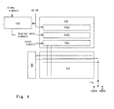
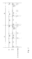
- Fig. 4 is a block diagram showing a multi-gray scale EL display device.
- the display device shown here is of the type that obtains gray scale by inputting a digital signal into a source signal line driving circuit and uses a digital gray scale method. Particularly the case of using time division gray scale method for varying the luminance by controlling the period of time during which a pixel emits light will be described.
- the EL display device of Fig. 4 has a pixel portion 101 and a source signal line driving circuit 102 and a gate signal line driving circuit 103 which are arranged in the periphery of the pixel portion 101.
- the pixel portion and the driving circuits are composed of thin film transistors (hereinafter referred to as TFTs) formed on a substrate.
- An external switch 116 for controlling the EL driving voltage is connected to the pixel portion 101.
- the source signal line driving circuit 102 includes, basically, a shift register 102a, a latch (A) 102b and a latch (B) 102c.
- the shift register 102a receives input of a clock signal (CLK) and a start pulse (SP).
- CLK clock signal
- SP start pulse
- the latch (A) 102b receives input of digital data signals (denoted by VD in Fig. 4) whereas the latch (B) 102c receives input of latch signals (denoted by S_LAT in Fig. 4).
- the digital data signals VD to be inputted to the pixel portion 101 are generated in a time division gray scale data signal generating circuit 114.
- This circuit converts video signals that are analog signals or digital signals containing image information into the digital data signals VD for time division gray scale.
- the circuit 114 also generates a timing pulse or the like that is necessary for time division gray scale display.
- the time division gray scale data signal generating circuit 114 includes means for dividing one frame period into a plurality of sub-frame periods in accordance with n bit gray scale (n is an integer of 2 or greater), means for selecting either a writing period or a display period in each of the plural sub-frame periods, and means for setting the length of the display period.
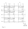
- the pixel portion 101 is structured generally as shown in Fig. 5.
- the pixel portion 101 is provided with gate signal lines (G1 to Gy) to which a selecting signal is inputted and source signal lines (also called data signal lines) (S1 to Sx) to which a digital data signal is inputted.
- the digital data signal refers to a digital video signal.
- the pixel portion also has power supply lines (V1 to Vx) parallel to the source signal lines (S1 to Sx).
- the electric potential of the power supply lines (V1 to Vx) is called a power supply electric potential.
- Wirings (Vb1 to Vby) are provided in parallel with the gate signal lines (G1 to Gy). The wirings (Vb1 to Vby) are connected to the external switch 116.
- a plurality of pixels 104 are arranged in matrix in the pixel portion 101.
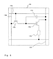
- One of the pixels 104 is enlarged and shown in Fig. 6.
- reference symbol 1701 denotes a TFT functioning as a switching element (hereinafter referred to as switching TFT).
- 1702 denotes a TFT functioning as an element for controlling a current supplied to an EL element 1703 (current controlling element) (The TFT will be called a driving TFT).
- Designated by 1704 is a capacitor storage.
- the switching TFT 1701 has a gate electrode connected to a gate signal line 1705 that is one of the gate signal lines (G1 to Gy) to which a gate signal is inputted.
- the switching TFT 1701 has a source region and a drain region one of which is connected to a source signal line 1706 and the other of which is connected to a gate electrode of the driving TFT 1702 and to the capacitor storage 1704.
- the source signal line 1706 is one of the source signal lines (S1 to Sx) to which a digital data signal is inputted.
- the driving TFT 1702 has a source region and a drain region one of which is connected to a power supply line 1707 and the other of which is connected to the EL element 1703.
- the power supply line 1707 is one of the power supply lines (V1 to Vx).
- the capacitor storage 1704 is connected to the power supply line 1707 that is one of the power supply lines (V1 to Vx).
- the EL element 1703 is composed of an anode, a cathode, and an EL layer interposed between the anode and the cathode.
- the anode When the anode is connected to the source region or the drain region of the driving TFT 1702, the anode serves as a pixel electrode whereas the cathode serves as an opposite electrode.
- the cathode when the cathode is connected to the source region or the drain region of the driving TFT 1702, the cathode serves as the pixel electrode whereas the anode serves as the opposite electrode.
- the electric potential of the opposite electrode is herein called an opposite electric potential. The difference in electric potential between the opposite electrode and the pixel electrode generates the EL driving voltage, which is applied to the EL layer.
- the opposite electrode of the EL element 1703 is connected to the external switch 116 through one of the wirings (Vb1 to Vby). (See Fig. 5.)
- Fig. 7 shows a timing chart thereof.
- one frame period is divided into n sub-frame periods (SF 1 to SF n ).
- a period during which one image is displayed using all of the pixels in the pixel portion is defined as one frame period (F).
- one frame period is set to about 1/60 second. With the period set to this long, human eyes do not recognize flicker in animated images displayed.
- the number of sub-frame periods in one frame period also increases and the driving circuits (the source signal line driving circuit and the gate signal line driving circuit), the source signal line driving circuit in particular, has to be driven at a higher frequency.
- Each sub-frame period is divided into a wiring period (Ta) and a display period (Ts).
- the writing period is a period for inputting signals into all of the pixels in one sub-frame period.
- the display period (also called a lights-on period) is a period for choosing whether or not the EL element emits light so that an image is displayed.
- the EL driving voltage shown in Fig. 7 corresponds to the EL driving voltage of the EL element when the EL element is caused to emit light.
- the EL driving voltage of the EL element in the pixel which is designated to emit light is in the level that does not cause the EL element to emit light, e.g., 0 V, during the writing period.
- the EL driving voltage thereof is in the level that allows the EL element to emit light.
- the opposite electric potential is controlled by the external switch 116 shown in Figs. 4 and 5. During the writing period, the opposite electric potential is kept at the same level as the power supply electric potential. On the other hand, the opposite electric potential is changed in the display period so as to generate an electric potential difference between the opposite electric potential and the power supply electric potential which causes the EL element to emit light.
- a gate signal is inputted to the gate signal line G1 to turn every switching TFT 1701 connected to the gate signal line G1 ON.
- a TFT being turned ON means that the gate voltage of the TFT is changed to make the source-drain thereof conductive.
- the writing period is started and digital data signals are inputted to the source signal lines (S1 to Sx). At this point, the opposite electric potential is kept at the same level as the power supply electric potential of the power supply lines (V1 to Vx).
- the digital data signals contain information of '0' or '1'.
- the digital data signals of '0' and '1' are signals having Hi voltage and Lo voltage, respectively.
- the digital data signals inputted to the source signal lines (S1 to Sx) are inputted to the gate electrode of each driving TFT 1702 through each switching TFT 1701 that has been turned ON.
- the capacitor storage 1704 also receives input of a digital data signal to hold it in.
- Selecting signals are successively inputted to the gate signal lines G2 to Gy to repeat the above operation until all of the pixels receive input of the digital data signals and the inputted digital data signals are held in the respective pixels.
- a period it takes for the digital data signals to be inputted to all of the pixels in each sub-frame period is the writing period.
- every switching TFT 1701 is turned OFF.
- a TFT being turned OFF means that the gate voltage of the TFT is changed to make the source-drain thereof unconductive.
- the external switch 116 connected to the opposite electrode is used to change the electric potential difference between the opposite electric potential and the power supply electric potential to a degree that causes the EL element to emit light.
- the driving TFT 1702 When a digital data signal has information of '0', the driving TFT 1702 is turned OFF and the EL element 1703 does not emit light. When a digital data signal has information of '1' on the other hand, the driving TFT 1702 is turned ON. Then the pixel electrode of the EL element 1703 is kept at the power supply electric potential and the EL element 1703 emits light. In this way, information contained in a digital data signal determines whether the EL element emits light or not. Every pixel whose EL element is designated to emit light is simultaneously lit up, and the lit-up pixels together form an image. A period during which the display by the pixels lasts is the display period.
- the writing periods (Ta 1 to Ta n ) in the n sub-frame periods (SF 1 to SF n ) have the same length.
- the sub-frame periods SF 1 to SF n have display periods Ts 1 to Ts n , respectively.
- Display of desired gray scales within the range of 2 n gray scales can be obtained through combinations of the display periods.
- a writing period is started again so that all the pixels receive digital data signals to start the display period.
- one of the display periods Ts 1 to Ts (n-1) is started. Here, given pixels are lit up for the period Ts (n-1) .
- One frame period is completed when n sub-frame periods have come and gone.
- the cumulative length of the display periods during which a pixel is lit up determines the gray scale of the pixel.
- the luminance is 75%. If the pixel is designated to emit light during the display periods Ts 3 , Ts 5 and Ts 8 , the luminance may be 16%.
- An object of the present invention is to improve the image quality of an EL display device, in particular, an EL display device using a bottom gate TFT.
- the object will be detailed below.
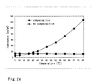
- the amount of current flowing into an EL element in a pixel is desirably kept constant throughout the display period of each sub-frame period. In actuality, however, the amount of current varies depending on the temperature.
- Fig. 18 is a graph showing the temperature characteristic of the EL element.
- the axis of abscissa shows the applied voltage that is applied between two electrodes of the EL element.
- the axis of ordinate shows the amount of current flowing into the EL element.
- Temperature T 1 is higher than temperature T 2 , which is higher than temperature T 3 .
- the graph shows that the same level of voltage applied between the electrodes of the EL element in the pixel portion does not always cause the same amount of current to flow through the EL element; the amount of current flowing into the EL element may increase as the temperature of the EL layer rises, depending on the temperature characteristic of the EL element.
- the amount of current flowing through the EL element in the pixel portion varies depending on the temperature at which the EL display device is used (hereinafter referred to as surrounding temperature), whereby the luminance of the EL element in the pixel portion is changed. Therefore the accuracy in gray scale display cannot be maintained, contributing to impaired reliability of EL display devices.
- Another object of the present invention is to control those change in luminance and increase in power consumption of the EL element due to a change in surrounding temperature.
- bottom gate TFTs have the following two problems.
- bottom gate TFTs side walls of a gate electrode has to be gentle because, according to the manufacturing process, an insulating film and a semiconductor thin film are to be formed thereon. Therefore, the width of the gate electrode (gate length) in bottom gate TFTs cannot be as small as the width of a gate electrode (gate length) in top gate TFTs, where side walls of the gate electrode are not required to be so gentle.
- a gate electrode is formed under a semiconductor thin film that is to be used as a source region and a drain region and hence the semiconductor thin film is convexed. If a polycrystalline film such as a polysilicon film is used as the convex semiconductor thin film, the crystallinity of the film is inferior to that of a polycrystalline film formed on a flat surface, and characteristics such as an electric field effect mobility (mobility) are also poor.
- the frequency characteristic of a driver circuit composed of a bottom gate TFT is inferior to the frequency characteristic of a driver circuit composed of a top gate TFT.
- the invention aims at providing a display device which is capable of controlling the change in luminance and increase in current consumption of an EL element due to a change in surrounding temperature, and which can obtain a larger screen, higher definition and more gray scales despite the inferior frequency characteristic of a source signal line driving circuit that is composed of a bottom gate TFT.
- an EL element for monitoring the temperature (hereinafter referred to as monitoring EL element) is provided in an EL display device.
- One electrode of the temperature monitoring EL element is connected to a constant current generator.
- the temperature characteristic of the monitoring EL element is utilized to keep the amount of current flowing into an EL element of a pixel constant.
- a video signal is subjected to time base expansion so as to give margin to sampling of the video signal in a source signal line driving circuit.
- a display device comprising a plurality of EL elements of a plurality of pixels and a monitoring EL element, characterized in that the temperature characteristic of the monitoring EL element is used to reduce a change in amount of current flowing through the plural EL elements due to temperature change.
- a display device comprising:
- a display device comprising:
- a display device comprising:
- a display device comprising:
- a display device comprising:
- the first electrode is an anode and the second electrode is a cathode in both of the monitoring EL element and the EL element.
- the first electrode is a cathode and the second electrode is an anode in both of the monitoring EL element and the EL element.
- a display device characterized in that at least one of the buffer amplifier and the constant current generator is composed of a thin film transistor formed on the same substrate on which the thin film transistor of each pixel is formed.
- a display device characterized in that at least one of the buffer amplifier, the constant current generator and the adder circuit is composed of a thin film transistor formed on the same substrate on which the thin film transistor of each pixel is formed.
- a display device characterized in that at least one of the buffer amplifier and the constant current generator is composed of a TFT formed on the same substrate on which the switching TFT and the driving TFT are formed.
- a display device characterized in that at least one of the buffer amplifier, the constant current generator and the adder circuit is composed of a TFT formed on the same substrate on which the switching TFT and the driving TFT are formed.
- a display device comprising:
- a display device comprising:
- a display device comprising:
- a display device comprising:
- the TFT constituting the source signal line driving circuit is a bottom gate TFT.
- a display device characterized in that the EL element uses an EL layer emitting monochrome light and color conversion layers in combination to provide color display.
- a display device characterized in that the EL element uses an EL layer emitting white light and color filters in combination to provide color display.
- a display device characterized in that the EL layer of the EL element is formed from a low molecular weight organic material or a polymer organic material.
- the low molecular weight organic material contains Alq 3 (tris-8-quinolilite-aluminum) or TPD (triphenylamine derivative).
- the polymer organic material contains PPV (polyphenylene vinylene), PVK (polyvinyl carbazole) or polycarbonate.
- a display device characterized in that the EL layer of the EL element is formed from an inorganic material.
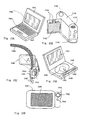
- a computer there may be provided a computer, a television set, a telephone, a monitor device and a navigation system for automobiles, each of which employs the display device.
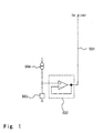
- Reference symbol 501 denotes a power supply line.
- the power supply line herein corresponds to a wiring for providing one electrode of an EL element (not shown) in a pixel portion with a given electric potential in response to a digital data signal inputted to a source signal line.
- the electric potential of the power supply line is called a power supply electric potential.
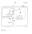
- Reference symbol 502 denotes a buffer amplifier, 503, a monitoring EL element, and 504, a constant current generator.
- One electrode of the monitoring EL element 503 is connected to the constant current generator 504, so that a constant amount of current flows through the monitoring EL element 503.
- the temperature of an EL layer of the EL element changes, the amount of current flowing into the monitoring EL element 503 does not change but instead the electric potential of the electrode of the monitoring EL element 503 which is connected to the constant current generator 504 changes.
- the monitoring EL element 503 and an EL element in each pixel are manufactured such that the relation of the amount of current flowing into the element to the level of voltage applied between two electrodes of the element is the same for both the monitoring EL element 503 and the pixel EL element at the same temperature.
- an electrode of the pixel EL element (pixel electrode) which is connected to the power supply line 501 is an anode if an electrode of the monitoring EL element 503 which is connected to the buffer amplifier 502 is an anode.
- the electrode of the monitoring EL element 503 which is connected to the buffer amplifier 502 is a cathode
- the electrode of the pixel EL element (pixel electrode) which is connected to the power supply line 501 is a cathode.
- An electrode of the monitoring EL element 503 which is not connected to the buffer amplifier 502 and an opposite electrode of the pixel portion EL element are given here almost the same electric potential.
- the buffer amplifier 502 has two input terminals and one output terminal. One of the input terminals is a non-inversion input terminal (+) and the other is an inversion input terminal (-). The electric potential of one electrode of the monitoring EL element 503 is given to the non-inversion input terminal of the buffer amplifier 502.
- the output terminal of the buffer amplifier is connected to the power supply line 501.
- the non-inversion input terminal of the buffer amplifier is connected to the output terminal of the buffer amplifier.
- the buffer amplifier is a circuit for preventing load such as wiring capacitance of the power supply line 501 from changing the electric potential of the electrode of the monitoring EL element 503 which is connected to the constant current generator 504. Accordingly, the electric potential given to the non-inversion input terminal of the buffer amplifier 502 is outputted from the output terminal without being changed by load such as wiring capacitance of the power supply line 501 to be given as the power supply electric potential to the power supply line 501.
- the power supply electric potential changes such that the amount of current flowing into the EL element is kept constant even when the surrounding temperature changes to change the temperature of the EL layers of the monitoring EL element 503 and of the pixel portion EL element. This prevents the change in luminance and increase in current consumption due to a change in surrounding temperature.
- the buffer amplifier 502 may be formed on the same substrate as the pixel portion or on an IC chip. The same applies to the monitoring EL element 503 and the constant current generator 504.
- the monitoring EL element 503 may be included in the pixel portion or may be provided separately from the pixel portion.
- a source signal line driving circuit composed of the bottom gate TFT is divided into several blocks. Each of the blocks simultaneously processes signals associated with some source signal lines, thereby increasing the processing speed of the source signal line driving circuit.
- FIG. 17 is a schematic diagram of the source signal line driving circuit.
- the source signal line driving circuit is divided into blocks associated with outputs to k source signal lines.
- a latch (A) and a latch (B) each consist of m blocks (the latch (A) has a latch (A), 1 to a latch (A), m, and the latch (B) has a latch (B), 1 to a latch (B), m).
- Each block consists of k latch circuits.
- a digital data signal VD inputted from the external is divided into k parts.
- the digital data signal VD divided into k parts is obtained by using an external time division signal generating circuit to convert a digital video signal into a signal for the time division gray scale display described above, subjecting to time base expansion a signal of a writing period in each sub-frame period of the converted signal, and converting the expanded signal into a parallel signal for the respective signals associated with the k source signal lines.
- a circuit for conducting the time base expansion is provided separately from and outside of the display device.
- the block latch (A), 1 In response to a signal from a shift register, the block latch (A), 1 simultaneously samples the k parts of the digital data signal VD which are associated with the outputs to the k source signal lines. Similarly, the rest of the blocks of the latch (A) (the latch (A), 2 to the latch (A), m) are selected in order until the k parts of the digital data signal VD which are associated with the outputs to all source signal lines S_1 to S_mk are held in the latch (A). Thereafter, a latch pulse is inputted to the latch (B). Upon input of the latch pulse, the signals held in the blocks of the latch (A) are inputted to the latch (B) all at once, and outputted to the source signal lines S_1 to S_mk.
- Embodiment Modes 1 and 2 can be carried out in combination without restriction.
- This embodiment gives a description about a case of using a temperature compensation circuit having a structure different from the structure shown in Fig. 1 in accordance with Embodiment Mode 1.
- Fig. 2 shows the structure of a temperature compensation circuit according to this embodiment.
- Reference symbol 501 denotes a power supply line, 502, a buffer amplifier, 503, a monitoring EL element, 504, a constant current generator, and 505, an adder circuit.
- One electrode of the monitoring EL element 503 is connected to the constant current generator 504, so that a constant amount of current flows through the monitoring EL element 503.
- the temperature of an EL layer of the EL element changes, the amount of current flowing into the monitoring EL element 503 does not change but instead the electric potential of the electrode of the monitoring EL element 503 which is connected to the constant current generator 504 changes.
- the monitoring EL element 503 and an EL element (not shown) in each pixel are manufactured such that the relation of the amount of current flowing into the element to the level of voltage applied between two electrodes of the element is the same for both the monitoring EL element 503 and the pixel EL element at the same temperature.
- an electrode of the pixel EL element (pixel electrode) which is connected to the power supply line 501 is an anode if an electrode of the monitoring EL element 503 which is connected to the buffer amplifier 502 is an anode.
- the electrode of the monitoring EL element 503 which is connected to the buffer amplifier 502 is a cathode
- the electrode of the pixel EL element (pixel electrode) which is connected to the power supply line 501 is a cathode.
- An electrode of the monitoring EL element 503 which is not connected to the buffer amplifier 502 and an opposite electrode of the pixel portion EL element are given here almost the same electric potential.
- the buffer amplifier 502 has two input terminals and one output terminal. One of the input terminals is a non-inversion input terminal (+) and the other is an inversion input terminal (-). The electric potential of one electrode of the monitoring EL element 503 is given to the non-inversion input terminal of the buffer amplifier 502.
- the buffer amplifier is a circuit for preventing load such as wiring capacitance of the power supply line 501 from changing the electric potential of the electrode of the monitoring EL element 503 which is connected to the constant current generator 504. Accordingly, the electric potential given to the non-inversion input terminal of the buffer amplifier 502 is outputted from the output terminal without being changed by load such as wiring capacitance of the power supply line 501 and the adder circuit 505 to be given to the adder circuit 505.
- a certain level of electric potential is added to or subtracted from the electric potential of the output terminal of the buffer amplifier 502 which has been given to the adder circuit 505.
- the electric potential given to the adder circuit is multiplied several folds. Thereafter, the electric potential of the adder circuit is given to the power supply line 501 as the power supply electric potential.
- Fig. 3 shows a detailed circuit diagram of the adder circuit according to this embodiment.
- the adder circuit 505 has a first resister 521, a second resister 522, an adder circuit power supply 525 and a non-inversion amplifier circuit 520.
- the non-inversion amplifier circuit 520 is composed of a third resister 523, a fourth resister 524, a non-inversion amplifier circuit power supply 526 and an amplifier 527.
- One terminal of the first resister 521 is an input terminal (IN) of the adder circuit.
- the other terminal of the first resister 521 is connected to one terminal of the second resister 522.
- the other terminal of the second resister 522 is connected to the adder circuit power supply 525.
- the output from between the first resister 521 and the second resister 522 is inputted to a non-inversion input terminal (+) of the amplifier 527 in the non-inversion amplifier circuit 520.
- One terminal of the third resister 523 is connected to an output terminal of the amplifier 527 whereas the other terminal of the third resister 523 is connected to an inversion input terminal of the amplifier 527.
- the output from between the third resister 523 and the inversion input terminal of the amplifier 527 is inputted to one terminal of the fourth resister 524.
- the other terminal of the fourth resister 524 is connected to the non-inversion amplifier circuit power supply 526.
- the output from between the third resister 523 and the output terminal of the amplifier 527 is outputted from an output terminal (OUT) of the adder circuit 505.
- the power supply electric potential changes such that the amount of current flowing into the pixel portion EL element is kept constant even when the surrounding temperature changes to change the temperature of the EL layers of the monitoring EL element 503 and of the pixel portion EL element. Therefore the luminance of the pixel portion EL element can be kept constant irrespective of a change in surrounding temperature of the EL display device.
- the presence of the adder circuit 505 eliminates the need to set the electric potential of the power supply line 501 (power supply electric potential) to the same level as the electric potential of the electrode of the monitoring EL element 503 which is connected to the constant current generator 504.
- the amount of current flowing through the buffer amplifier 502, the monitoring element 503 and the constant current generator 504 can thus be limited. As a result, power consumption of the device can be suppressed.
- the structure of the adder circuit 505 is not limited to the one shown in Fig. 3.
- the buffer amplifier 502 may be formed on the same substrate as the pixel portion or on an IC chip. The same applies to the monitoring EL element 503, the constant current generator 504 and the adder circuit 505.
- the monitoring EL element 503 may be included in the pixel portion or may be provided separately from the pixel portion.
- a description given in this embodiment is on an example of the structure of a buffer amplifier in a temperature compensation circuit of a display device according to the present invention.
- Fig. 8 shows a case of manufacturing the buffer amplifier from a TFT that has the same structure as a TFT in a pixel.
- the buffer amplifier is composed of TFTs 1901 to 1909, a capacitor 1910, constant current generators 1911 and 1912, and power supply lines 1930 and 1931.
- TFTs 1901, 1902, 1906 and 1909 are n-channel TFTs whereas the TFTs 1903 to 1905 and the TFTs 1907 and 1908 are p-channel TFTs.
- the electric potential of the power supply line 1930 at this point is set higher than the electric potential of the power supply line 1931.
- the electric potential of the power supply line 1931 is 0 V in Fig. 8, but it is not limited thereto.
- the polarity of the TFTs according to this embodiment is not limited to the above. That is, any of the TFTs 1901 to 1909 can choose an n-channel TFT or a p-channel TFT. However, the TFTs 1901 and 1902 constituting a differential amplifier 1921 have to have the same polarity and almost the same characteristics. Also, the TFTs 1903 and 1904 constituting a current mirror circuit 1922 have to have the same polarity and almost the same characteristics.
- Source regions of the TFTs 1901 and 1902 connected to each other are connected to the constant current generator 1911.
- the electric potential difference makes the amount of current flowing between a drain and a source of the TFT 1901 different from that of the TFT 1902.
- the currents in the TFTs 1901 and 1902 are denoted by i1 and i2, respectively.
- the current mirror circuit 1922 is composed of the TFTs 1903 and 1904. Source regions of the TFTs 1903 and 1904 are both connected to the power supply line 1930. A drain region of the TFT 1904 and a gate electrode thereof are connected to each other. A gate electrode of the TFT 1903 is connected to the gate electrode of the TFT 1904, and hence the gate electrodes of the two TFTs have the same electric potential. Accordingly, the amount of current flowing between a source and a drain of the TFT 1903 is the same as the amount of current flowing between a source and a drain of the TFT 1904. This means that a current i3 has to be inputted to the current mirror circuit 1922. The current i3 corresponds to the difference between the currents i1 and i2 respectively flowing through the TFTs 1901 and 1902 of the differential amplifier 1921.
- the current i3 is supplied from the capacitor 1910.
- the supply of the current i3 increases an electric potential difference V1 between electrodes of the capacitor 1910.
- the electric potential difference V1 is then inputted to a source ground amplifier circuit 1923.
- the source ground amplifier circuit 1923 is composed of the TFT 1905.
- the electric potential difference V1 inputted serves as the electric potential between a gate and a source of the TFT 1905.
- a current i4 is supplied from the power supply line 1930 in accordance with the electric potential difference V1.
- the constant current generator 1912 only generates a constant current i0.
- a current i5 corresponding to the difference between the current i4 and the current i0 is therefore inputted to a source follower buffer circuit 1924.
- the current i5 is increased in accordance with the amplified electric potential difference V1.
- the source follower buffer circuit 1924 is composed of the TFTs 1906 and 1907.
- the current i5 inputted from the source ground amplifier circuit 1923 is inputted to a gate electrode of the TFT 1906. With the input current i5, the gate electric potential of the TFT 1906 is raised to increase a current i6 flowing between a source and a drain of the TFT 1906. As a result, a larger amount of current than in the buffer amplifier is outputted.
- the buffer amplifier When an output terminal of the buffer amplifier and the inversion input terminal thereof are connected to each other here, the buffer amplifier operates such that the electric potential of the output terminal obtains the same level as the electric potential of the non-inversion input terminal.
- the buffer amplifier thus outputs from its output terminal the same level of voltage as the signal voltage inputted to the non-inversion input terminal.
- the structure of the buffer amplifier in the display device of the present invention is not limited to the one shown in Fig. 8, but every known buffer amplifier can be used.
- This embodiment can be carried out in combination with Embodiment 1 without restriction.
- This embodiment describes a method of simultaneously manufacturing TFTs for a pixel portion of a display device according to the present invention and TFTs for driver circuit portions that are provided in the periphery of the pixel portion.
- a CMOS circuit that is a basic unit of a driver circuit is illustrated as the driver circuit portions.
- gate electrodes 502 to 505 are first formed from a chromium film on a glass substrate 501.
- a silicon oxynitride film (an insulating film of SiOxNy) is used to form a gate insulating film 507 on the gate electrodes.
- an amorphous silicon film is formed and crystallized by laser annealing.
- the crystallized film is patterned to form semiconductor films 508 to 511 that are crystalline silicon films. The steps up through this point can be carried out with known materials and known techniques.
- insulating films 512 to 515 are formed from a silicon oxide film on the semiconductor films 508 to 511.
- the semiconductor films are doped with phosphorus or arsenic through the insulating films.
- a known technique can be used as the doping method.
- n type impurity regions 516 to 519 are formed.
- the n type impurity regions 516 to 519 contain phosphorus or arsenic in a concentration of 1 x 10 20 to 1 x 10 21 atoms/cm 3 . (Fig. 19B)
- the insulating films 512 to 515 are patterned by back side exposure to form insulating films (channel protection films) 520 to 523.
- doping of phosphorus or arsenic is again conducted by a known technique.
- n type impurity regions 524 to 531 are formed.
- the n type impurity regions 524 to 531 contain phosphorus or arsenic in a concentration of 1 x 10 17 to 1 x 10 19 atoms/cm 3 . (Fig. 19C)
- resist masks 532 and 533 are formed to conduct doping of boron by a known technique.
- p type impurity regions 534 to 537 are formed.
- the p type impurity regions 534 to 537 contain boron in a concentration of 3 x 10 20 to 5 x 10 21 atoms/cm 3 .
- the p type impurity regions 534 to 537 have already been doped with phosphorus or arsenic, now that they are doped with boron in a concentration 3 times the phosphorus or arsenic concentration or more, the conductivity of the regions 534 to 537 is shifted from n type to p type completely. (Fig. 19D)
- the resist masks 532 and 533 are then removed, and a first interlayer insulating film 538 having a laminate structure of a silicon oxide film and a silicon oxynitride film is formed.
- a contact hole is formed in the first interlayer insulating film 538 to form wirings 539 to 544 in which a molybdenum film and a tungsten film are layered.
- a second interlayer insulating film 545, a pixel electrode 546, banks 547a and 547b, an EL layer 548, a cathode 549 and a protective film 550 are formed as shown in Fig. 20.
- a light emitting device having the sectional structure of Fig. 20 is thus completed.
- This embodiment can be carried out in combination with either Embodiment 1 or Embodiment 2 without restriction.
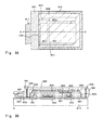
- Fig. 9A is a top view of an EL display device using the present invention.
- Fig. 9B shows a cross-sectional view in which Fig. 9A is cut along the line A-A'.
- reference numeral 4010 is a substrate
- reference numeral 4011 is a pixel portion
- reference numeral 4012 is a source signal side driver circuit
- reference numeral 4013 is a gate signal side driver circuit.
- the driver circuits are connected to external equipment, through an FPC 4017, via wirings 4014and 4016.
- Reference numeral 4015 is a wiring for the power source supply line.
- a covering material 6000, a sealing material (also referred to as a housing material) 7000, and an airtight sealing material (a second sealing material) 7001 are formed so as to enclose at least the pixel portion, preferably the driver circuits and the pixel portion, at this point.
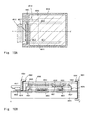
- Fig. 9B is a cross sectional structure of the EL display device of the present invention.
- a driver circuit TFT 4022 (note that a CMOS circuit in which an n-channel TFT and a p-channel TFT are combined is shown in the figure here), a pixel portion TFT 4023 (note that only a driver TFT for controlling the current flowing to an EL element is shown here) are formed on a base film 4021 on a substrate 4010.
- the TFTs may be formed using a known structure (a top gate structure or a bottom gate structure).
- a pixel electrode 4027 is formed on an interlayer insulating film (leveling film) 4026 made from a resin material.
- the pixel electrode is formed from a transparent conducting film for electrically connecting to a drain of the pixel TFT 4023.
- An indium oxide and tin oxide compound (referred to as ITO) or an indium oxide and zinc oxide compound can be used as the transparent conducting film.
- An insulating film 4028 is formed after forming the pixel electrode 4027, and an open portion is formed on the pixel electrode 4027.
- the EL layer 4029 may be formed having a lamination structure, or a single layer structure, by freely combining known EL materials (such as a hole injecting layer, a hole transporting layer, a light emitting layer, an electron transporting layer, and an electron injecting layer). A known technique may be used to determine which structure to use. Further, EL materials exist as low molecular weight materials and high molecular weight (polymer) materials. Evaporation is used when using a low molecular weight material, but it is possible to use easy methods such as spin coating, printing, and ink jet printing when a high molecular weight material is employed.
- the EL layer is formed by evaporation using a shadow mask.
- Color display becomes possible by forming emitting layers (a red color emitting layer, a green color emitting layer, and a blue color emitting layer), capable of emitting light having different wavelengths, for each pixel using a shadow mask.
- emitting layers a red color emitting layer, a green color emitting layer, and a blue color emitting layer
- methods such as a method of combining a charge coupled layer (CCM) and color filters, and a method of combining a white color light emitting layer and color filters may also be used.
- the EL display device can also be made to emit a single color of light.
- a cathode 4030 is formed on the EL layer. It is preferable to remove as much as possible any moisture or oxygen existing in the interface between the cathode 4030 and the EL layer 4029. It is therefore necessary to use a method of depositing the EL layer 4029 and the cathode 4030 in an inert gas atmosphere or within a vacuum.
- the above film deposition becomes possible in embodiment 4 by using a multi-chamber method (cluster tool method) film deposition apparatus.
- a lamination structure of a LiF (lithium fluoride) film and an Al (aluminum) film is used in embodiment 3 as the cathode 4030.
- a 1 nm thick LiF (lithium fluoride) film is formed by evaporation on the EL layer 4029, and a 300 nm thick aluminum film is formed on the LiF film.
- An MgAg electrode, a known cathode material, may of course also be used.
- the wiring 4016 is then connected to the cathode 4030 in a region denoted by reference numeral 4031.
- the wiring 4016 is an electric power supply line for imparting a predetermined voltage to the cathode 4030, and is connected to the FPC 4017 through a conducting paste material 4032.
- the contact holes may be formed at the time of etching the interlayer insulating film 4026 (when forming a contact hole for the pixel electrode) and at the time of etching the insulating film 4028 (when forming the opening portion before forming the EL layer). Further, when etching the insulating film 4028, etching may be performed all the way to the interlayer insulating film 4026 at one time. A good contact hole can be formed in this case, provided that the interlayer insulating film 4026 and the insulating film 4028 are the same resin material.
- a passivation film 6003, a filling material 6004, and the covering material 6000 are formed covering the surface of the EL element thus made.
- the sealing material 7000 is formed between the covering material 6000 and the substrate 4010, so as to surround the EL element portion, and the airtight sealing material (the second sealing material) 7001 is formed on the outside of the sealing material 7000.
- the filling material 6004 functions as an adhesive for bonding the covering material 6000 at this point.
- PVC polyvinyl chloride
- epoxy resin silicone resin
- PVB polyvinyl butyral
- EVA ethylene vinyl acetate
- spacers may be contained within the filling material 6004.
- the spacers may be a powdered substance such as BaO, giving the spacers themselves the ability to absorb moisture.
- the passivation film 6003 can relieve the spacer pressure. Further, a film such as a resin film can be formed separately from the passivation film 6003 to relieve the spacer pressure.
- a glass plate, an aluminum plate, a stainless steel plate, an FRP (fiberglass-reinforced plastic) plate, a PVF (polyvinyl fluoride) film, a Mylar film, a polyester film, and an acrylic film can be used as the covering material 6000.
- PVF polyvinyl fluoride
- Mylar film a polyester film
- acrylic film an acrylic film
- PVB or EVA it is preferable to use a sheet with a structure in which several tens of aluminum foil is sandwiched by a PVF film or a Mylar film.
- the covering material 6000 it is necessary for the covering material 6000 to have light transmitting characteristics.
- the wiring 4016 is electrically connected to the FPC 4017 through a gap between the sealing material 7001 and the substrate 4010. Note that although an explanation of the wiring 4016 has been made here, the wirings 4014 and 4015 are also electrically connected to the FPC 4017 by similarly passing underneath the sealing material 7001 and sealing material 7000.
- the covering material 6000 is bonded after forming the filling material 6004, and the sealing material 7000 is attached so as to cover the lateral surfaces (exposed surfaces) of the filling material 6004, but the filling material 6004 may also be formed after attaching the covering material 6000 and the sealing material 7000.
- a filling material injection opening is formed through a gap formed by the substrate 4010, the covering material 6000, and the sealing material 7000.
- the gap is set into a vacuum state (a pressure equal to or less than 10 -2 Torr), and after immersing the injection opening in the tank holding the filling material, the air pressure outside of the gap is made higher than the air pressure within the gap, and the filling material fills the gap.
- Fig. 10A is a top view of an EL display device of embodiment 5, and Fig. 10B shows a cross sectional diagram in which Fig. 10A is cut along the line A-A'.
- manufacturing is performed through the step of forming the passivation film 6003 covering the EL element.
- the filling material 6004 is formed so as to cover the EL element.
- the filling material 6004 also functions as an adhesive for bonding the covering material 6000.
- PVC polyvinyl chloride
- epoxy resin epoxy resin
- silicone resin silicone resin
- PVB polyvinyl butyral
- EVA ethylene vinyl acetate
- spacers may be contained within the filling material 6004.
- the spacers may be a powdered substance such as BaO, giving the spacers themselves the ability to absorb moisture.
- the passivation film 6003 can relieve the spacer pressure. Further, a film such as a resin film can be formed separately from the passivation film 6003 to relieve the spacer pressure.
- a glass plate, an aluminum plate, a stainless steel plate, an FRP (fiberglass-reinforced plastic) plate, a PVF (polyvinyl fluoride) film, a Mylar film, a polyester film, and an acrylic film can be used as the covering material 6000.
- PVF polyvinyl fluoride
- Mylar film a polyester film
- acrylic film an acrylic film
- PVB or EVA it is preferable to use a sheet with a structure in which several tens of aluminum foil is sandwiched by a PVF film or a Mylar film.
- the covering material 6000 it is necessary for the covering material 6000 to have light transmitting characteristics.
- the frame material 6001 is attached so as to cover the lateral surfaces (exposed surfaces) of the filling material 6004.
- the frame material 6001 is bonded by the sealing material (which functions as an adhesive) 6002.
- the sealing material 6002 It is preferable to use a light hardening resin as the sealing material 6002 at this point, but provided that the heat resistance characteristics of the EL layer permit, a thermal hardening resin may also be used.
- the sealing material 6002 be a material which, as much as possible, does not transmit moisture and oxygen. Further, a drying agent may also be added to an inside portion of the sealing material 6002.
- the wiring 4016 is electrically connected to the FPC 4017 through a gap between the sealing material 6002 and the substrate 4010. Note that although an explanation of the wiring 4016 has been made here, the wirings 4014 and 4015 are also electrically connected to the FPC 4017 by similarly passing underneath the sealing material 6002.
- the covering material 6000 is bonded, and the frame material 6001 is attached so as to cover the lateral surfaces (exposed surfaces) of the filling material 6004, after forming the filling material 6004 in Figs. 10A and 10B, but the filling material 6004 may also be formed after attaching the covering material 6000 and the frame material 6001.
- a filling material injection opening is formed through a gap formed by the substrate 4010, the covering material 6000, and the frame material 6001.
- the gap is set into a vacuum state (a pressure equal to or less than 10 -2 Torr), and after immersing the injection opening in the tank holding the filling material, the air pressure outside of the gap is made higher than the air pressure within the gap, and the filling material fills the gap.
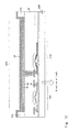
- FIG. 11 A more detailed cross sectional structure of a pixel portion is shown here in Fig. 11.
- a switching TFT 3502 formed on a substrate 3501 is manufactured by using a known method in Fig. 11.
- a single gate structure is used in embodiment 6. Note that although a single gate structure is used in embodiment 6, a double gate structure, a triple gate structure, and a multi gate structure possessing a greater number of gates may also be used.
- a single gate structure of the driver TFT 3503 is shown in the figures in embodiment 6, but a multi-gate structure in which a plurality of TFTs are connected in series may also be used.
- a structure in which a plurality of TFTs are connected in parallel, effectively partitioning into a plurality of channel forming regions, and which can perform radiation of heat with high efficiency, may also be used. Such structure is effective as a countermeasure against deterioration due to heat.
- the driver TFT 3503 is formed by a known method.
- the drain wiring 35 of the switching TFT 3502 is connected electrically to the gate wiring 37 of the driver TFT 3503.
- the drain wiring 40 of the driver TFT 3503 is connected to the cathode 43 of EL element.
- a source region 34 of the driver TFT 3503 is connected to an electric power supply line (not shown in the figures), and a constant voltage is always applied.
- a leveling film 42 from an insulating resin film is formed on the switching TFT 3502 and the driver TFT 3503. It is extremely important to level the step due to the TFTs using the leveling film 42. An EL layer formed later is extremely thin, so there are cases in which defective light emissions occur. Therefore, to form the EL layer with as level a surface as possible, it is preferable to perform leveling before forming a pixel electrode.
- reference numeral 43 denotes a pixel electrode (EL element cathode) made from a conducting film with high reflectivity, and this is electrically connected to a drain region 40 of the driver TFT 3503. It is preferable to use a low resistance conducting film, such as an aluminum alloy film, a copper alloy film, and a silver alloy film, or a laminate of such films. Of course, a lamination structure with another conducting film may also be used.
- a low resistance conducting film such as an aluminum alloy film, a copper alloy film, and a silver alloy film, or a laminate of such films.
- a lamination structure with another conducting film may also be used.
- a light emitting layer 45 is formed in the middle of a groove (corresponding to a pixel) formed by banks 44a and 44b, which are formed by insulating films (preferably resins). Note that only one pixel is shown in the figures here, but the light emitting layer may be divided to correspond to each of the colors R (red), G (green), and B (blue).
- a ⁇ -conjugate polymer material is used as an organic EL material. Polyparaphenylene vinylenes (PPVs), polyvinyl carbazoles (PVKs), and polyfluoranes can be given as typical polymer materials.
- cyano-polyphenylene vinylene may be used as a red light radiating luminescence layer
- polyphenylene vinylene may be used as a green light radiating luminescence layer
- polyphenylene vinylene or polyalkylphenylene may be used as a blue light radiating luminescence layer.
- the film thicknesses may be between 30 and 150 nm (preferably between 40 and 100 nm).
- An EL layer (a layer for emitting light and for performing carrier motion for such) may be formed by freely combining light emitting layers, electric charge transporting layers, and electric charge injecting layers.
- embodiment 6 shows an example of using a polymer material as a light emitting layer, but a low molecular weight organic EL material may also be used.
- inorganic materials such as silicon carbide, as an electric charge transporting layer or an electric charge injecting layer.
- Known materials can be used for these organic EL materials and inorganic materials.
- An anode 47 is then formed on the light emitting layer 45 from a transparent conducting film.
- the light generated by the light emitting layer 45 is radiated toward the upper surface (toward the reverse direction to the substrate on which is formed TFT) in embodiment 6, and therefore the anode must be transparent to light.
- An indium oxide and tin oxide compound, or an indium oxide and zinc oxide compound can be used for the transparent conducting film.
- it is formed after forming the low heat resistance light emitting and hole injecting layers it is preferable to use a material which can be deposited at as low a temperature as possible.
- An EL element 3505 is complete at the point where the anode 47 is formed.
- the EL element 3505 here is formed by the pixel electrode (cathode) 43, the light emitting layer 45, and the anode 47.
- the pixel electrode 43 is nearly equal in area to the pixel, and consequently the entire pixel functions as an EL element. Therefore, the light emitting efficience is extremely high, and a bright image display becomes possible.
- a second passivation film 48 is then formed on the anode 47 in embodiment 6.
- a silicon nitride film or a silicon oxynitride film as the second passivation film 48.
- the purpose of this is the isolation of the EL element from the outside, and this is meaningful in preventing degradation due to oxidation of the organic EL material, and in controlling gaseous emitted from the organic EL material. The reliability of the EL display device can thus be raised.
- n-channel TFTs and p-channel TFTs may be used for the driver TFT.
- the driver TFT be an n-channel TFT. Note that it is possible to implement the constitution of embodiment 6 by freely combining it with the constitutions of any of embodiments 1 to 5.
- This embodiment gives a description on the structure obtained by inverting the structure of the EL element 3505 in the pixel portion shown in Embodiment 6. The description will be given with reference to Fig. 12.
- the structure of this embodiment is different from the structure of Fig. 11 described in Embodiment 6 regarding only with the EL element and a driving TFT.
- the same components as those in Fig. 11 are denoted by the same reference symbols and explanations thereof will be omitted.
- a switching TFT may be an n-channel TFT or a p-channel TFT and the same applies to a driving TFT.
- the driving TFT is desirably a p-channel TFT if a pixel electrode of an EL element is an anode.
- a driving TFT 3703 is a p-channel TFT and can be manufactured by using a known method.
- the driving TFT 3703 of this embodiment has a drain wiring 55 connected to an anode 50 of an EL element 3701.
- the driving TFT 3703 has a source region 56 connected to a power supply line (not shown).
- a switching TFT 3502 here is an n-channel TFT.
- a gate electrode 57 of the driving TFT 3703 is electrically connected to a drain wiring 35 of the switching TFT 3502.
- a transparent conductive film is used for the pixel electrode (anode) 50 in this embodiment.
- the film used is a conductive film containing a compound of indium oxide and zinc oxide.
- a conductive film containing a compound of indium oxide and tin oxide may of course be used instead.
- a light emitting layer 52 is formed from polyvinyl carbazole by solution coating.
- a cathode 54 is formed from an aluminum alloy. In this case, the cathode 54 also functions as a passivation film. The EL element 3701 is thus completed.
- light generated in the light emitting layer 52 is emitted toward a substrate on which the TFTs are formed as indicated by the arrow.
- Embodiments 1 through 5 This embodiment can be combined freely with Embodiments 1 through 5.
- This embodiment describes the structure of a source signal line driving circuit.
- the source signal line driving circuit is fabricated by forming a bottom gate TFT on an insulating substrate through a process as the one shown in Embodiment 3.
- Fig. 15 focuses on a latch (A) and a latch (B) in one block.
- a shift register 8801, latches (A) 8802 and latches (B) 8803 are arranged as shown in Fig. 15.
- a pair of latches (A) 8802 and a pair of latches (B) 8803 are associated with four source signal lines S_a to S_d.
- the description given in this embodiment is of a case where a digital video signal is divided into four parts and then inputted, so that the four signals are sampled at the same time.
- the present invention is not limited to this case and the signal may be divided into k parts (k is an arbitrary integer greater than 1) to sample the k signals.
- a level shifter, a buffer or the like for changing the amplitude of the voltage of a signal is not provided in this embodiment. However, it may be provided if a designer finds it suitable.
- a clock signal CLK, a clock signal CLKB obtained by inverting the polarity of CLK, a start pulse signal SP, and a drive direction switching signal SL/R are inputted to the shift register 8801 from their respective wirings shown in Fig. 15.
- a digital data signal VD inputted from the external is subjected to time base expansion and divided into four parts, which are inputted to the latches (A) 8802 from the wirings shown in Fig. 15.
- a latch signal S_LAT and a signal S_LATb obtained by inverting the polarity of S_LAT are inputted to the latches (B) 8803 from their respective wirings shown in Fig. 15.
- the latches (A) 8802 With an input of a signal from the shift register 8801, the latches (A) 8802 receive from signal lines of digital data divided into four parts the four parts of the digital data signal VD to sample the four signals simultaneously and hold them in. In response to input of the latch signal S_LAT and the signal S_LATb, the signals held in the latches (A) are sent to the latches (B) 8803 all at once to be outputted to the source signal lines S_a to S_d.
- the portion 8804 that is a part of the latches (A) 8802 has two clocked inverters and two inverters.
- Fig. 16 shows a top view of the portion 8804 that is a part of the latches (A) 8802.
- 831a and 831b are active layers of TFTs that constitute one of the inverters of the portion 8804 that is a part of the latches (A) 8802.
- Reference symbol 836 denotes a common gate electrode of the TFTs constituting the one inverter.
- the other inverter of the portion 8804 that is a part of the latches (A) 8802 is composed of TFTs whose active layers are denoted by 832a and 832b.
- gate electrodes 837a and 837b are provided on the active layers 832a and 832b.
- the gate electrodes 837a and 837b are electrically connected to each other.
- Denoted by 833a and 833b are active layers of TFTs that constitute one of the clocked inverters of the portion 8804 that is a part of the latches (A) 8802.
- gate electrodes 838a and 838b are formed to provide a double gate structure.
- the gate electrode 838b and a gate electrode 839 are formed to provide a double gate structure.
- Denoted by 834a and 834b are active layers of TFTs that constitute the other clocked inverter of the portion 8804 that is a part of the latches (A) 8802.
- the gate electrode 839 and a gate electrode 840 are formed to provide a double gate structure.
- the gate electrode 840 and a gate electrode 841 are formed to provide a double gate structure.
- the analog method refers to a method in which the luminance of pixels is varied by inputting an analog signal into a source signal line in a display device.
- the description given here deals with a case where an analog signal is inputted to a source signal line driving circuit to output the analog signal to a source signal line.
- Fig. 21 shows an example of the source signal line driving circuit employing the analog method.
- Fig. 21 focuses on one block in the source signal line driving circuit with the block associated with outputs of signal lines S_a to S_d.
- a signal sent from a shift register 8801 simultaneously turns TFTs 2101a to 2101d ON, starting simultaneous sampling of four parts of the analog data signal VA.
- the description given in this embodiment is of the case where four parts of the analog data signal VA which are to be inputted to four source signal lines are sampled at once.
- the source signal line driving circuit of a display device according to the present invention is not limited thereto.
- the invention can use a source signal line driving circuit in which the analog data signal VA is divided into arbitrary number of parts that are to be inputted to the same number of source signal lines and the parts are sampled at the same time.
- Fig. 22A shows an example of a circuit for subjecting an analog video signal to time base expansion so as to generate the analog data signal VA (hereinafter referred to as time base expansion circuit).
- Switches SW1 to SW4 are opened and closed one by one in response to an opening and closing signal shown in a timing chart of Fig. 22B.
- the analog video signals are thus sampled and held in storage capacitors 2201 to 2204.
- the signals held are outputted through buffers 2211 to 2214.
- the analog data signal VA divided into four parts is thus generated.
- the description given in this embodiment takes as an example the time base expansion circuit for converting an analog video signal into four parts of analog data signal VA which are associated with four source signal lines.
- the time base expansion circuit of a display device according to the present invention is not limited thereto.
- the invention can use a time base expansion circuit for converting an analog video signal into an arbitrary number of analog data signals associated with the same number of source signal lines.
- Embodiments 1 through 7 This embodiment can be combined freely with Embodiments 1 through 7.
- the material used in the EL layer of the EL element in the EL display of the present invention is not limited to an organic EL material, and the present invention can be implemented using an inorganic EL material.
- inorganic EL materials have an extremely high driver voltage, and therefore TFTs which have voltage resistance characteristics such that they are able to withstand such a high voltage must be used.
- Embodiment 9 Furthermore, it is possible to freely combine the constitution of Embodiment 9 with the constitution of any of Embodiments 1 to 8.
- an organic material used as an EL layer may be either a low molecular organic material or a polymer (high molecular) organic material.
- the low molecular organic material materials are known centering on Alq 3 (tris-8-quinolylite-aluminum), TPD (triphenylamine derivative) or the like.
- polymer organic material ⁇ -cooperative polymer materials can be given.
- PPV polyphenylenevynilene
- PVK polyvynilcarbazole
- polycarbonate or the like can be given.
- the polymer (high molecular) organic material can be formed with a simple thin film formation method such as the spin coating method (which is referred to also as solution application method), the dipping method, the dispense method, the printing method, the ink jet method or the like.
- the polymer organic material has a high heat endurance compared with the low molecular organic material.
- the electron transport layer and the positive hole transport layer may be formed of inorganic material such as, for example, a amorphous semiconductor formed of amorphous Si or amorphous Si 1-x C x or the like.
- the amorphous semiconductor In the amorphous semiconductor, a large quantity of trap level is present, and at the same time, the amorphous semiconductor forms a large quantity of interface levels at an interface at which the amorphous semiconductor contacts other layers. As a consequence, the EL element can emit light at a low voltage, and at the same time, an attempt can be made to provide a high luminance.
- a dopant (impurity) is added to the organic EL layer, and the color of light emission of the organic EL layer may be changed.
- This dopant includes DCM1, nile red, lubren, coumarin 6, TPB and quinaquelidon.
- Embodiment 10 may be combined freely with any of the structures in Embodiments 1 through 8.
- This embodiment gives a description on a case of manufacturing an EL display device in accordance with the present invention with reference to Figs. 13A and 13B.
- Fig. 13A is a top view of an active matrix substrate with an EL element formed and enclosed thereon. Regions 801, 802 and 803 sectioned by dotted lines are a source signal line driving circuit, a gate signal line driving circuit and a pixel portion, respectively. Reference symbol 804 denotes a covering member, 805, a first sealing member, and 806, a second sealing member. A filler 807 (See Fig. 13B) is provided in a space between the active matrix substrate and the covering member within the surrounding first sealing member 805.
- Denoted by 808 is a connection wiring for transmitting signals to be inputted to the source signal line driving circuit 801, the gate signal line driving circuit 802 and the pixel portion 803.
- the wiring receives a video signal, a clock signal and the like from an FPC (flexible printed circuit) 809 that serves as a terminal for connecting the display device with external equipment.
- FPC flexible printed circuit
- Fig. 13A is cut along the line A-A' and the sectional view thereof is shown in Fig. 13B.
- Figs. 13A and 13B the same components are denoted by the same reference symbols.
- the pixel portion 803 and the source signal line driving circuit 801 are formed on a substrate 800.
- the pixel portion 803 is comprised of a plurality of pixels each having a TFT 851 that controls the amount of current flowing into an EL element (driving TFT), a pixel electrode 852 that is electrically connected to a drain region of the TFT 851, and other components.
- the driving TFT 851 is a p-channel TFT.
- the driving TFT will be described as a representative of TFTs that constitute the pixel portion.
- a CMOS circuit in which an n-channel TFT 853 and a p-channel TFT 854 are combined complementarily will be described as a representative of TFTs that constitute the source signal line driving circuit 801.
- Each pixel has, under the pixel electrode 852, one of a color filter (R) 855, a color filter (G) 856 and a color filter (B) (not shown).
- the color filter (R) is a color filter for extracting red light
- the color filter (G) is a color filter for extracting green light
- the color filter (B) is a color filter for extracting blue light.
- the color filter (R) 855 is provided in a red light emitting pixel
- the color filter (G) 856 is provided in a green light emitting pixel
- the color filter (B) is provided in a blue light emitting pixel.
- the first thing given as an effect of these color filters is that the purity of emitted light is improved in terms of color.
- the EL element of a red light emitting pixel emits red light (toward the pixel electrode side in this embodiment) and the emitted red light passes through the color filter for extracting red light to gain an improved purity of red color.
- the EL element used in these conventional cases is one that emits white light. With the EL element emitting white light, red light is extracted by cutting other wavelengths of light, which invites lowering of luminance. On the other hand, this embodiment in which red light emitted from an EL element passes through the color filter for extracting red light does not lower the luminance.
- the pixel electrode 852 is formed from a transparent conductive film and functions as an anode of the EL element.
- An insulating film 857 is formed on each side of the pixel electrode 852, and a light emitting layer 858 for emitting red light and a light emitting layer 859 for emitting green light are further formed.
- a light emitting layer for emitting blue light is formed in a pixel adjacent to the pixel having the light emitting layer 859.
- color display is obtained by pixels emitting red light, green light and blue light.
- the pixel having the light emitting layer for emitting blue light is provided with the color filter for extracting blue light.
- the light emitting layer may be used in combination with one or more of an electron injection layer, an electron transportation layer, a hole transportation layer and a hole injection layer to form a laminate.
- a cathode 860 of the EL element is formed on the light emitting layers from a light-shielding conductive film.
- the cathode 860 is shared by all the pixels, and is electrically connected to the FPC 809 through the connection wiring 808.
- the first sealing member 805 is formed using a dispenser or the like, a spacer (not shown) is sprayed, and the covering member 804 is bonded.
- the filler 807 is filled into a region surrounded by the active matrix substrate, the covering member 804 and the first sealing member 805 by vacuum injection.
- the filler 807 is doped in advance with barium oxide as a hygroscopic substance 861.
- the filler is doped with the hygroscopic substance in this embodiment, it may be contained in the filler in chunks dispersed throughout the filler.
- the hygroscopic substance may be used as a material for the spacer.
- the filler 807 is then cured by irradiation of ultraviolet light or by heating. Thereafter, an opening (not shown) formed in the first sealing member 805 is closed. After closing the opening in the first sealing member 805, the connection wiring 808 is electrically connected to the FPC 809 with a conductive material 862.
- the second sealing member 806 is placed so as to cover the exposed portion of the first sealing member 805 and a part of the FPC 809.
- the second sealing member 806 can be formed from the same material as the first sealing member 805.
- the EL element is enclosed in the filler 807 in accordance with the method described above, whereby the EL element is completely shut out from the outside and moisture and substances promoting oxidation of the organic material, such as oxygen, can be prevented from entering the EL element from the outside.
- an EL display device of high reliability can be manufactured.
- Embodiments 1 through 10 This embodiment can be combined freely with Embodiments 1 through 10.
- This embodiment shows an example of the case where the traveling direction of the light emitted from the EL element and arrangement of the color filters are different from those of the EL display device shown in Embodiment 11.
- the description will be given with reference to Fig. 14.
- the basic structure of Fig. 14 is the same as Fig. 13, and only modified components receive new reference symbols and description.
- a pixel portion 901 is comprised of a plurality of pixels each having a TFT 902 that controls the amount of current flowing into the EL element (driving TFT), a pixel electrode 903 that is electrically connected to a drain region of the TFT 902, and other components.
- an n-channel TFT is used for the driving TFT 902 in the pixel portion 901.
- the drain of the driving TFT 902 is electrically connected to the pixel electrode 903, which is formed from a light-shielding conductive film.
- the pixel electrode 903 serves as a cathode of the EL element in this embodiment.
- a transparent conductive film 904 shared by the pixels are formed.
- the transparent conductive film 904 serves as an anode of the EL element.
- Another feature of this embodiment is that a color filter (R) 905, a color filter (G) 906 and a color filter (B) (not shown) are formed in the covering member 804.
- a color filter (R) 905, a color filter (G) 906 and a color filter (B) are formed in the covering member 804.
- Forming the color filter (R) 905, the color filter (G) 906 and the color filter (B) (not shown) in the covering member 804 as in this embodiment is advantageous, for the steps of manufacturing an active matrix substrate can be reduced in number to thereby improve the yield and the throughput.
- Embodiments 1 through 10 This embodiment can be combined freely with Embodiments 1 through 10.
- This embodiment describes a case of actually constructing from elements the constant current generator of the temperature compensation circuit which has the structure shown in Fig. 1 in accordance with Embodiment Mode 1.
- Fig. 23 is a circuit diagram showing the structure of the temperature compensation circuit according to this embodiment.
- a temperature compensation circuit 701 is composed of a constant current generator 704, a monitoring EL element 703 and a buffer amplifier 702.
- An output of the constant current generator 704 is connected to one electrode of the monitoring EL element 703 and to an input terminal of the buffer amplifier 702.
- An output of the buffer amplifier 702 serves as an output of the temperature compensation circuit 701.
- the output of the temperature compensation circuit 701 is connected to a power supply line 705, which gives an electric potential to a pixel electrode of an EL element (not shown) in a pixel through the source-drain of a driving TFT (not shown).
- the constant current generator 704 is composed of an amplifier 706, a variable resister 707 and a transistor 708.
- the transistor 708 is a p-channel TFT in the description given in this embodiment but the transistor is not limited thereto.
- the polarity of this transistor may be of an n-channel TFT or of a p-channel TFT.
- the transistor may be a bipolar transistor.
- the transistor 708 has a source region connected to an inversion input terminal (-) of the amplifier 706 and to the variable resister 707, and has a drain region connected to an output terminal of the constant current generator 704. A gate electrode of the transistor 708 is connected to an output terminal of the amplifier 706.
- a constant voltage V2 is inputted to a non-inversion terminal (+) of the amplifier 706.
- the amplifier 706, the variable resister 707 and the transistor 708 that constitute the constant current generator may be formed on an IC chip or on the same substrate which has an insulating surface and on which pixels are formed.
- the monitoring EL element 703 connected to the constant current generator 701 operates so as to cause a constant current generated by the constant current generator 701 to flow. If there is a change in surrounding temperature while the display device is in use, the amount of current flowing through the monitoring EL element 703 does not change. Instead, the electric potential of the electrode of the monitoring EL element which is connected to the constant current generator 704 is changed.
- the monitoring EL element 703 and an EL element in a pixel are manufactured such that the relation of the amount of current flowing into the element to the level of voltage applied between two electrodes of the element is the same for both the monitoring EL element 703 and the pixel EL element at the same temperature.
- the electric potential of an electrode of the monitoring EL element 703 which is not connected to the constant current generator 704 and to a non-inversion input terminal of the buffer amplifier 702 is set to the same level as the electric potential of an opposite electrode of the EL element in each pixel.
- an electrode of a pixel EL element (pixel electrode) which is connected to the output terminal of the buffer amplifier has to be an anode if the electrode of the monitoring EL element which is connected to the output of the buffer amplifier and to the constant current generator is an anode.
- the electrode of the pixel EL element (pixel electrode) which is connected to the output terminal of the buffer amplifier has to be a cathode if the electrode of the monitoring EL element which is connected to the output of the buffer amplifier and to the constant current generator is a cathode.
- the pixel electrode of the pixel EL element is an anode.
- an electric potential V1 is set to a level higher than an input electric potential V2.
- the electric potential V1 is the electric potential of the terminal of the variable resister 707 which is not connected to the transistor 708 and to the non-inversion input terminal of the amplifier 706.
- the input electric potential V2 is the electric potential inputted to the non-inversion input terminal of the amplifier 706.
- An electric potential V3 of the anode of the monitoring EL element 703 is set to a level lower than the electric potential V2.
- the electric potential V3 of the anode of the monitoring EL element 703 is changed to change the voltage between the two electrodes thereof
- the electric potential of the anode of the pixel EL element is similarly changed to change the voltage between the two electrodes thereof.
- This change in voltage works to cause a constant current provided by the constant current generator 704 at the surrounding temperature to flow also into the pixel portion EL element.
- the pixel portion EL element receives a constant current irrespective of a change in surrounding temperature and emits light of constant luminance.
- the structure of the constant current generator is not limited to the structure of 704, but a constant current generator circuit of any known structure can be employed without restriction.
- Embodiments 1 through 12 This embodiment can be combined freely with Embodiments 1 through 12.
- This embodiment shows results of measuring a change in luminance of a pixel EL element in a display device of the present invention which is caused by a change in temperature.
- Fig. 24 is a graph showing the measurement results.
- the axis of ordinate shows the luminance (cd/m 2 ) and the axis of abscissa shows the temperature (°C).
- the graph also shows results of measuring a change in luminance of a pixel EL element due to a temperature change in a display device that does not have a temperature compensation circuit.
- the luminance of an EL element is increased as the temperature rises.
- the luminance of an EL element is almost constant irrespective of the temperature.
- the present invention thus can prevent the change in luminance of a pixel portion EL element in a display device due to a temperature change by using a temperature compensation circuit.
- the invention is also advantageous in the following point.
- the EL layer constituting the EL element is formed mainly from organic compounds and degradation thereof is a problem required to be solved. Comparing the case in which a pixel EL element emits light upon receiving a constant current flowing between the electrodes of the element with the case in which a pixel EL element emits light upon receiving a constant voltage applied between the electrodes of the element, lowering of luminance due to the degradation of EL element is less in the former case. Therefore inputting a constant current into a pixel EL element in order to cause the element to emit light as in this embodiment is capable of limiting the lowering of luminance due to the degradation of its EL layer.
- the EL display device manufactured by applying the present invention can be used in various kinds of electronic equipment.
- the electronic equipment, which incorporates the EL display device manufactured by applying the present invention as the display medium, are explained below.
- Such kind of electronic equipment include personal computer, a portable information medium (such as a mobile computer, mobile telephone, a electronic book and so forth), a game machine, a TV receiver, a video camera, a digital camera, a telephone, a head mounted display (goggle type display), an image playback device, a car navigation system and the like. Examples of those are shown in Fig. 9.
- Fig. 25A shows a personal computer, which contains a main body 2001, a casing 2002, a display portion 2003, a keyboard 2004 and the like.
- the EL display device of the present invention can be used in the display portion 2003 of the personal computer.
- Fig. 25B shows a video camera, which contains a main body 2100, a display portion 2102, a sound input portion 2103, operation switches 2104, a battery 2105, an image receiving portion 2106 and the like.
- the EL display device of the present invention can be used in the display portion 2102 of the video camera.
- Fig. 25C shows a portion (right side) of a head mounted display, which contains a main body 2301, a signal cable 2302, a head fixing band 2303, a screen monitor 2304, an optical system 2305, a display portion 2306 and the like.
- the EL display device of the present invention can be used in the display portion 2306 of the head mounted display.
- Fig. 25D shows an image playback device equipped with a recording medium (specifically, a DVD playback device), which contains a main body 2401, a recording medium (such as a CD, an LD or a DVD) 2402, operation switches 2403, a display portion (a) 2404, a display portion (b) 2405 and the like.
- the display portion (a) 2404 is mainly used for displaying image information.
- the display portion (b) 2405 is mainly used for displaying character information.
- the EL display device of the present invention can be used in the display portion (a) 2404 and the display portion (b) 2405 of the image playback device equipped with the recording medium. Note that the present invention can be applied to devices such as a CD playback device and a game machine as the image playback device equipped with the recording medium.
- Fig. 25E shows a mobile computer, which contains a main body 2501, a camera portion 2502, an image receiving portion 2503, operation switches 2504, a display portion 2505 and the like.
- the EL display device of the present invention can be used in the display portion 2505 of the mobile computer.
- the EL material may be used in a front type or rear type projector.
- the electronic equipment of this embodiment can be realized using the constitution in which Embodiments 1 to 14 are freely combined.
- Conventional EL display devices have problems such as fluctuation in luminance and increased current consumption, for the amount of current flowing into an EL element is changed by a change in surrounding temperature while the devices are in use depending on the temperature characteristic of the EL element even if the voltage applied to the EL element is the same.
- a source signal line driving circuit composed of a bottom gate TFT is a hindrance for a display device to obtain a larger screen and more gray scales because of its poor frequency characteristic and resulting slow operation.
- the present invention employs the above structures to keep the amount of current flowing into a pixel portion EL element constant against a change in temperature.
- the invention also gives a margin to sampling of a video signal in the source signal line driving circuit by subjecting the video signal to time base expansion.
- the invention can provide a display device which can prevent the change in luminance and increase in current consumption of the EL element due to a change in surrounding temperature and which can obtain a larger screen, higher definition and more gray scales by compensating the frequency characteristic of a source signal line driving circuit that is composed of a bottom gate TFT.
Landscapes
- Engineering & Computer Science (AREA)
- Physics & Mathematics (AREA)
- Computer Hardware Design (AREA)
- General Physics & Mathematics (AREA)
- Theoretical Computer Science (AREA)
- Electroluminescent Light Sources (AREA)
- Control Of Indicators Other Than Cathode Ray Tubes (AREA)
- Control Of El Displays (AREA)
Applications Claiming Priority (2)
| Application Number | Priority Date | Filing Date | Title |
|---|---|---|---|
| JP2000176246 | 2000-06-13 | ||
| JP2000176246 | 2000-06-13 |
Publications (3)
| Publication Number | Publication Date |
|---|---|
| EP1168291A2 true EP1168291A2 (de) | 2002-01-02 |
| EP1168291A3 EP1168291A3 (de) | 2010-10-06 |
| EP1168291B1 EP1168291B1 (de) | 2017-05-24 |
Family
ID=18677986
Family Applications (1)
| Application Number | Title | Priority Date | Filing Date |
|---|---|---|---|
| EP01114361.7A Expired - Lifetime EP1168291B1 (de) | 2000-06-13 | 2001-06-13 | Anzeigegerät |
Country Status (5)
| Country | Link |
|---|---|
| US (2) | US6528951B2 (de) |
| EP (1) | EP1168291B1 (de) |
| KR (1) | KR100813082B1 (de) |
| CN (1) | CN100416865C (de) |
| TW (1) | TW512304B (de) |
Cited By (18)
| Publication number | Priority date | Publication date | Assignee | Title |
|---|---|---|---|---|
| EP1193677A3 (de) * | 2000-09-29 | 2002-08-21 | Seiko Epson Corporation | Verfahren zur Ansteuerung einer elektrooptischen Vorrichtung, elektrooptische Vorrichtung und elektronisches Gerät |
| EP1363149A2 (de) * | 2002-05-13 | 2003-11-19 | Semiconductor Energy Laboratory Co., Ltd. | Optische Rückwandverdrahtung |
| US7190335B2 (en) | 2002-03-26 | 2007-03-13 | Semiconductor Energy Laboratory Co., Ltd. | Light emitting device and method of manufacturing the same |
| SG131756A1 (en) * | 2002-03-07 | 2007-05-28 | Semiconductor Energy Lab | Light emitting apparatus and method of fabricating the same |
| US7315295B2 (en) | 2000-09-29 | 2008-01-01 | Seiko Epson Corporation | Driving method for electro-optical device, electro-optical device, and electronic apparatus |
| US7482629B2 (en) | 2004-05-21 | 2009-01-27 | Semiconductor Energy Laboratory Co., Ltd. | Display device and electronic device |
| EP1774500A4 (de) * | 2004-07-23 | 2009-07-15 | Semiconductor Energy Lab | Anzeigeeinrichtung und ansteuerverfahren dafür |
| US7635863B2 (en) | 2005-10-18 | 2009-12-22 | Semiconductor Energy Laboratory Co., Ltd. | Display device and electronic apparatus having the display device |
| US7777232B2 (en) | 2005-04-11 | 2010-08-17 | Semiconductor Energy Laboratory Co., Ltd. | Display device and electronic device using the same |
| US8013809B2 (en) | 2004-06-29 | 2011-09-06 | Semiconductor Energy Laboratory Co., Ltd. | Display device and driving method of the same, and electronic apparatus |
| US8111215B2 (en) | 2004-05-22 | 2012-02-07 | Semiconductor Energy Laboratory Co., Ltd. | Display device and electronic device |
| US8154541B2 (en) | 2004-07-30 | 2012-04-10 | Semiconductor Energy Laboratory Co., Ltd. | Display device, driving method thereof and electronic appliance |
| US8194006B2 (en) | 2004-08-23 | 2012-06-05 | Semiconductor Energy Laboratory Co., Ltd. | Display device, driving method of the same, and electronic device comprising monitoring elements |
| US8421715B2 (en) | 2004-05-21 | 2013-04-16 | Semiconductor Energy Laboratory Co., Ltd. | Display device, driving method thereof and electronic appliance |
| US8681140B2 (en) | 2004-05-21 | 2014-03-25 | Semiconductor Energy Laboratory Co., Ltd. | Display device and electronic apparatus having the same |
| US8773333B2 (en) | 2002-10-31 | 2014-07-08 | Semiconductor Energy Laboratory Co., Ltd. | Display device and controlling method thereof |
| US9076383B2 (en) | 2002-05-15 | 2015-07-07 | Semiconductor Energy Laboratory Co., Ltd. | Display device |
| US11513405B2 (en) | 2018-04-26 | 2022-11-29 | Semiconductor Energy Laboratory Co., Ltd. | Display device and electronic device |
Families Citing this family (101)
| Publication number | Priority date | Publication date | Assignee | Title |
|---|---|---|---|---|
| TW468283B (en) * | 1999-10-12 | 2001-12-11 | Semiconductor Energy Lab | EL display device and a method of manufacturing the same |
| TW471011B (en) | 1999-10-13 | 2002-01-01 | Semiconductor Energy Lab | Thin film forming apparatus |
| TWM244584U (en) | 2000-01-17 | 2004-09-21 | Semiconductor Energy Lab | Display system and electrical appliance |
| US20010030511A1 (en) * | 2000-04-18 | 2001-10-18 | Shunpei Yamazaki | Display device |
| US6995753B2 (en) | 2000-06-06 | 2006-02-07 | Semiconductor Energy Laboratory Co., Ltd. | Display device and method of manufacturing the same |
| JP2002072963A (ja) * | 2000-06-12 | 2002-03-12 | Semiconductor Energy Lab Co Ltd | 発光モジュールおよびその駆動方法並びに光センサ |
| TW512304B (en) * | 2000-06-13 | 2002-12-01 | Semiconductor Energy Lab | Display device |
| US6828950B2 (en) * | 2000-08-10 | 2004-12-07 | Semiconductor Energy Laboratory Co., Ltd. | Display device and method of driving the same |
| TW550530B (en) * | 2000-10-27 | 2003-09-01 | Semiconductor Energy Lab | Display device and method of driving the same |
| JP3800050B2 (ja) * | 2001-08-09 | 2006-07-19 | 日本電気株式会社 | 表示装置の駆動回路 |
| CN107230450A (zh) * | 2001-09-21 | 2017-10-03 | 株式会社半导体能源研究所 | 显示装置及其驱动方法 |
| EP1450341A4 (de) * | 2001-09-25 | 2009-04-01 | Panasonic Corp | El-anzeigetafel und el-anzeigevorrichtung damit |
| JP5022547B2 (ja) * | 2001-09-28 | 2012-09-12 | キヤノン株式会社 | 画像形成装置の特性調整方法、画像形成装置の製造方法、画像形成装置及び特性調整装置 |
| US20030071821A1 (en) * | 2001-10-11 | 2003-04-17 | Sundahl Robert C. | Luminance compensation for emissive displays |
| US7224333B2 (en) * | 2002-01-18 | 2007-05-29 | Semiconductor Energy Laboratory Co. Ltd. | Display device and driving method thereof |
| US6933520B2 (en) * | 2002-02-13 | 2005-08-23 | Semiconductor Energy Laboratory Co., Ltd. | Light emitting device |
| JP3838964B2 (ja) | 2002-03-13 | 2006-10-25 | 株式会社リコー | 機能性素子基板の製造装置 |
| CN1543635A (zh) * | 2002-03-22 | 2004-11-03 | ���ձ�ӡˢ��ʽ���� | 图像显示装置 |
| WO2003092165A1 (fr) * | 2002-04-26 | 2003-11-06 | Toshiba Matsushita Display Technology Co., Ltd. | Circuits a semi-conducteur destines a commander par courant un affichage et affichage correspondant |
| KR20030086166A (ko) * | 2002-05-03 | 2003-11-07 | 엘지.필립스 엘시디 주식회사 | 유기전계 발광소자와 그 제조방법 |
| JP2003330420A (ja) * | 2002-05-16 | 2003-11-19 | Semiconductor Energy Lab Co Ltd | 発光装置の駆動方法 |
| US7184034B2 (en) | 2002-05-17 | 2007-02-27 | Semiconductor Energy Laboratory Co., Ltd. | Display device |
| TWI360098B (en) * | 2002-05-17 | 2012-03-11 | Semiconductor Energy Lab | Display apparatus and driving method thereof |
| SG119186A1 (en) * | 2002-05-17 | 2006-02-28 | Semiconductor Energy Lab | Display apparatus and driving method thereof |
| US7170479B2 (en) * | 2002-05-17 | 2007-01-30 | Semiconductor Energy Laboratory Co., Ltd. | Display device and driving method thereof |
| US7474285B2 (en) * | 2002-05-17 | 2009-01-06 | Semiconductor Energy Laboratory Co., Ltd. | Display apparatus and driving method thereof |
| JP3501155B1 (ja) * | 2002-07-03 | 2004-03-02 | 富士電機ホールディングス株式会社 | 有機elディスプレイおよびその製造方法 |
| US9153168B2 (en) * | 2002-07-09 | 2015-10-06 | Semiconductor Energy Laboratory Co., Ltd. | Method for deciding duty factor in driving light-emitting device and driving method using the duty factor |
| US20040031965A1 (en) * | 2002-08-16 | 2004-02-19 | Forrest Stephen R. | Organic photonic integrated circuit using an organic photodetector and a transparent organic light emitting device |
| CN100419837C (zh) * | 2002-08-21 | 2008-09-17 | 皇家飞利浦电子股份有限公司 | 显示器件及其显示驱动器件 |
| JP4194451B2 (ja) * | 2002-09-02 | 2008-12-10 | キヤノン株式会社 | 駆動回路及び表示装置及び情報表示装置 |
| AU2003276706A1 (en) * | 2002-10-31 | 2004-05-25 | Casio Computer Co., Ltd. | Display device and method for driving display device |
| CN1332448C (zh) * | 2002-12-03 | 2007-08-15 | 友达光电股份有限公司 | 有源式有机发光二极管的像素结构及其制造方法 |
| TW584820B (en) * | 2003-02-11 | 2004-04-21 | Au Optronics Corp | Organic light emitting display |
| CN1320515C (zh) * | 2003-02-24 | 2007-06-06 | 友达光电股份有限公司 | 有机发光显示器 |
| KR100832613B1 (ko) * | 2003-05-07 | 2008-05-27 | 도시바 마쯔시따 디스플레이 테크놀로지 컴퍼니, 리미티드 | El 표시 장치 |
| CN1784708A (zh) * | 2003-05-07 | 2006-06-07 | 东芝松下显示技术有限公司 | 电流输出型半导体电路、显示驱动用源极驱动器、显示装置、电流输出方法 |
| JP3897173B2 (ja) * | 2003-05-23 | 2007-03-22 | セイコーエプソン株式会社 | 有機el表示装置及びその製造方法 |
| KR100742063B1 (ko) * | 2003-05-26 | 2007-07-23 | 가시오게산키 가부시키가이샤 | 전류생성공급회로 및 표시장치 |
| US7053412B2 (en) * | 2003-06-27 | 2006-05-30 | The Trustees Of Princeton University And Universal Display Corporation | Grey scale bistable display |
| JP4304585B2 (ja) * | 2003-06-30 | 2009-07-29 | カシオ計算機株式会社 | 電流生成供給回路及びその制御方法並びに該電流生成供給回路を備えた表示装置 |
| JP4205629B2 (ja) * | 2003-07-07 | 2009-01-07 | セイコーエプソン株式会社 | デジタル/アナログ変換回路、電気光学装置及び電子機器 |
| US20050007026A1 (en) * | 2003-07-07 | 2005-01-13 | Shin-Tai Lo | Method and apparatus for generating uniform images of active matrix OLED display devices |
| JP4103079B2 (ja) * | 2003-07-16 | 2008-06-18 | カシオ計算機株式会社 | 電流生成供給回路及びその制御方法並びに電流生成供給回路を備えた表示装置 |
| KR100552963B1 (ko) | 2003-08-28 | 2006-02-15 | 삼성에스디아이 주식회사 | 휘도 불균일이 개선된 평판표시장치 |
| KR100560786B1 (ko) * | 2003-10-28 | 2006-03-13 | 삼성에스디아이 주식회사 | 전자계방지보호회로의 배치가 용이한 유기전계발광표시장치 |
| KR100666548B1 (ko) * | 2003-11-26 | 2007-01-09 | 삼성에스디아이 주식회사 | 트라이오드 정류스위치를 포함하는 표시장치 |
| US20070132674A1 (en) * | 2003-12-02 | 2007-06-14 | Toshiba Matsushita Display Technology Co., Ltd. | Driving method of self-luminous type display unit, display control device of self-luminous type display unit, current output type drive circuit of self-luminous type display unit |
| KR100591548B1 (ko) * | 2003-12-30 | 2006-06-19 | 엘지.필립스 엘시디 주식회사 | 유기전계 발광소자 |
| KR100581903B1 (ko) | 2004-03-09 | 2006-05-22 | 삼성에스디아이 주식회사 | 전계 발광 디스플레이 장치 |
| US20050205880A1 (en) * | 2004-03-19 | 2005-09-22 | Aya Anzai | Display device and electronic appliance |
| US7764012B2 (en) * | 2004-04-16 | 2010-07-27 | Semiconductor Energy Laboratory Co., Ltd | Light emitting device comprising reduced frame portion, manufacturing method with improve productivity thereof, and electronic apparatus |
| US20050248517A1 (en) * | 2004-05-05 | 2005-11-10 | Visteon Global Technologies, Inc. | System and method for luminance degradation reduction using thermal feedback |
| US8581805B2 (en) * | 2004-05-21 | 2013-11-12 | Semiconductor Energy Laboratory Co., Ltd. | Display device and driving method thereof |
| CN100511371C (zh) * | 2004-05-21 | 2009-07-08 | 株式会社半导体能源研究所 | 显示装置和电子装置 |
| WO2005114630A1 (en) * | 2004-05-21 | 2005-12-01 | Semiconductor Energy Laboratory Co., Ltd. | Display device and electronic device |
| US8248392B2 (en) * | 2004-08-13 | 2012-08-21 | Semiconductor Energy Laboratory Co., Ltd. | Light emitting device using light emitting element and driving method of light emitting element, and lighting apparatus |
| KR101196656B1 (ko) * | 2004-08-13 | 2012-11-02 | 가부시키가이샤 한도오따이 에네루기 켄큐쇼 | 발광 장치 및 상기 발광 장치의 구동 방법 |
| JP4822387B2 (ja) * | 2004-08-31 | 2011-11-24 | 東北パイオニア株式会社 | 有機elパネルの駆動装置 |
| US7259405B2 (en) * | 2004-11-23 | 2007-08-21 | Au Optronics Corporation | Organic photoelectric device with improved electron transport efficiency |
| US7570233B2 (en) * | 2004-11-24 | 2009-08-04 | Semiconductor Energy Laboratory Co., Ltd. | Display device |
| US7365494B2 (en) | 2004-12-03 | 2008-04-29 | Semiconductor Energy Laboratory Co., Ltd. | Display device and manufacturing method thereof |
| US7442950B2 (en) * | 2004-12-06 | 2008-10-28 | Semiconductor Energy Laboratory Co., Ltd. | Light emitting device |
| US7812794B2 (en) * | 2004-12-06 | 2010-10-12 | Semiconductor Energy Laboratory Co., Ltd. | Display device and driving method thereof |
| KR100775057B1 (ko) * | 2004-12-13 | 2007-11-08 | 삼성전자주식회사 | 트랜지스터 정합 특성이 향상된 데이터 드라이브 집적회로를 구비한 디스플레이 장치 |
| CN101694766A (zh) * | 2005-05-02 | 2010-04-14 | 株式会社半导体能源研究所 | 发光器件、以及电子器具 |
| US7459850B2 (en) * | 2005-06-22 | 2008-12-02 | Eastman Kodak Company | OLED device having spacers |
| US8692740B2 (en) * | 2005-07-04 | 2014-04-08 | Semiconductor Energy Laboratory Co., Ltd. | Display device and driving method thereof |
| US7986287B2 (en) | 2005-08-26 | 2011-07-26 | Semiconductor Energy Laboratory Co., Ltd. | Display device and method of driving the same |
| KR100773088B1 (ko) * | 2005-10-05 | 2007-11-02 | 한국과학기술원 | 전류 귀환을 이용한 amoled 구동회로 |
| US20070126667A1 (en) * | 2005-12-01 | 2007-06-07 | Toshiba Matsushita Display Technology Co., Ltd. | El display apparatus and method for driving el display apparatus |
| US7995012B2 (en) * | 2005-12-27 | 2011-08-09 | Semiconductor Energy Laboratory Co., Ltd. | Light emitting device |
| EP1804229B1 (de) * | 2005-12-28 | 2016-08-17 | Semiconductor Energy Laboratory Co., Ltd. | Anzeigevorrichtung und Prüfungsverfahren dafür |
| KR101424784B1 (ko) * | 2006-01-10 | 2014-07-31 | 가부시키가이샤 한도오따이 에네루기 켄큐쇼 | 표시장치 및 그의 제조방법 |
| KR100714621B1 (ko) * | 2006-01-24 | 2007-05-07 | 삼성전기주식회사 | 온도보상기능을 갖는 led 구동 장치 |
| KR100965022B1 (ko) * | 2006-02-20 | 2010-06-21 | 도시바 모바일 디스플레이 가부시키가이샤 | El 표시 장치 및 el 표시 장치의 구동 방법 |
| US7639237B2 (en) * | 2006-03-03 | 2009-12-29 | Perkins Michael T | Roll-out touch screen support system (ROTS3) |
| TWI337725B (en) * | 2006-04-10 | 2011-02-21 | Chimei Innolux Corp | Data display method capable of releasing double image and improving mprt |
| KR101194858B1 (ko) | 2006-04-25 | 2012-10-26 | 엘지디스플레이 주식회사 | 전계발광 표시장치 및 그의 구동방법 |
| KR100812001B1 (ko) * | 2006-11-10 | 2008-03-10 | 삼성에스디아이 주식회사 | 유기전계발광 표시장치 및 그 제조방법 |
| US7877058B2 (en) * | 2006-11-10 | 2011-01-25 | Skyworks Solutions, Inc. | Compact low loss high frequency switch with improved linearity performance |
| US7714812B2 (en) * | 2006-11-28 | 2010-05-11 | Hong Fu Jin Precision Industry (Shen Zhen) Co., Ltd. | Driving circuit for providing constant current |
| JP2008225179A (ja) * | 2007-03-14 | 2008-09-25 | Sony Corp | 表示装置、表示装置の駆動方法、および電子機器 |
| JP5037221B2 (ja) * | 2007-05-18 | 2012-09-26 | 株式会社半導体エネルギー研究所 | 液晶表示装置及び電子機器 |
| JP2009037221A (ja) * | 2007-07-06 | 2009-02-19 | Semiconductor Energy Lab Co Ltd | 発光装置、電子機器および発光装置の駆動方法 |
| JP2009246127A (ja) * | 2008-03-31 | 2009-10-22 | Sumitomo Chemical Co Ltd | 有機エレクトロルミネッセンス素子及びその製造方法 |
| KR101574125B1 (ko) * | 2008-07-16 | 2015-12-04 | 삼성디스플레이 주식회사 | 유기 발광 표시 장치 및 그 제조 방법 |
| JP5250493B2 (ja) * | 2008-07-16 | 2013-07-31 | 株式会社半導体エネルギー研究所 | 発光装置 |
| KR101383950B1 (ko) | 2008-08-21 | 2014-04-14 | 엘지디스플레이 주식회사 | 유기발광 표시장치 |
| KR101002663B1 (ko) * | 2008-12-11 | 2010-12-21 | 삼성모바일디스플레이주식회사 | 유기 발광 표시 장치 |
| TWI424423B (zh) | 2010-10-20 | 2014-01-21 | Chunghwa Picture Tubes Ltd | 液晶顯示裝置及其驅動方法 |
| TWI481008B (zh) * | 2012-11-22 | 2015-04-11 | 隆達電子股份有限公司 | 發光裝置 |
| US9245935B2 (en) | 2013-04-02 | 2016-01-26 | Semiconductor Energy Laboratory Co., Ltd. | Light-emitting device |
| KR20150108463A (ko) * | 2014-03-17 | 2015-09-30 | 삼성디스플레이 주식회사 | 유기발광 표시장치 및 그의 제조방법 |
| WO2016108122A1 (en) | 2014-12-29 | 2016-07-07 | Semiconductor Energy Laboratory Co., Ltd. | Semiconductor device and display device having semiconductor device |
| JP6832634B2 (ja) | 2015-05-29 | 2021-02-24 | 株式会社半導体エネルギー研究所 | 半導体装置 |
| US10501003B2 (en) | 2015-07-17 | 2019-12-10 | Semiconductor Energy Laboratory Co., Ltd. | Semiconductor device, lighting device, and vehicle |
| JP6998690B2 (ja) | 2016-07-28 | 2022-01-18 | 株式会社半導体エネルギー研究所 | 情報端末 |
| GB2560315A (en) * | 2017-03-06 | 2018-09-12 | Innovative Tech Ltd | A safe conduit device |
| CN107464830A (zh) * | 2017-07-18 | 2017-12-12 | 武汉华星光电半导体显示技术有限公司 | 阵列基板及制作方法、显示面板 |
| US11217152B1 (en) * | 2020-06-16 | 2022-01-04 | Novatek Microelectronics Corp. | Source driver and driving circuit thereof |
Family Cites Families (74)
| Publication number | Priority date | Publication date | Assignee | Title |
|---|---|---|---|---|
| JPS5528247A (en) * | 1978-08-21 | 1980-02-28 | Hitachi Ltd | El element drive circuit |
| JPS55121782A (en) * | 1979-03-12 | 1980-09-19 | Clarion Co Ltd | Video code process system for television |
| JPH0192576A (ja) | 1987-10-02 | 1989-04-11 | Toyota Motor Corp | 内燃機関の点火装置 |
| GB8909011D0 (en) | 1989-04-20 | 1989-06-07 | Friend Richard H | Electroluminescent devices |
| US5170158A (en) * | 1989-06-30 | 1992-12-08 | Kabushiki Kaisha Toshiba | Display apparatus |
| JPH0594151A (ja) | 1991-08-08 | 1993-04-16 | Seiwa Denki Kk | Led点灯回路 |
| JP2894039B2 (ja) * | 1991-10-08 | 1999-05-24 | 日本電気株式会社 | 表示装置 |
| JPH05273941A (ja) * | 1991-11-14 | 1993-10-22 | Keyence Corp | 液晶表示装置の駆動電圧供給回路 |
| JPH05232903A (ja) * | 1992-01-28 | 1993-09-10 | Nec Corp | 液晶表示装置 |
| JP3230010B2 (ja) * | 1992-02-28 | 2001-11-19 | キヤノン株式会社 | 液晶カラー表示装置 |
| JPH06118910A (ja) | 1992-10-08 | 1994-04-28 | Alps Electric Co Ltd | 液晶表示装置の駆動方法 |
| JP3390214B2 (ja) | 1993-07-19 | 2003-03-24 | パイオニア株式会社 | 表示装置の駆動回路 |
| US5594463A (en) * | 1993-07-19 | 1997-01-14 | Pioneer Electronic Corporation | Driving circuit for display apparatus, and method of driving display apparatus |
| US5745085A (en) * | 1993-12-06 | 1998-04-28 | Fujitsu Limited | Display panel and driving method for display panel |
| US5734366A (en) * | 1993-12-09 | 1998-03-31 | Sharp Kabushiki Kaisha | Signal amplifier, signal amplifier circuit, signal line drive circuit and image display device |
| KR0163077B1 (ko) * | 1993-12-27 | 1999-01-15 | 사또오 후미오 | 표시장치 |
| KR100295712B1 (ko) * | 1994-03-11 | 2001-11-14 | 미다라이 후지오 | 컴퓨터디스플레이시스템컨트롤러 |
| JPH08146916A (ja) * | 1994-11-22 | 1996-06-07 | Nippondenso Co Ltd | 表示装置の駆動装置 |
| JPH08227283A (ja) * | 1995-02-21 | 1996-09-03 | Seiko Epson Corp | 液晶表示装置、その駆動方法及び表示システム |
| JP3234131B2 (ja) * | 1995-06-23 | 2001-12-04 | 株式会社東芝 | 液晶表示装置 |
| US5847516A (en) * | 1995-07-04 | 1998-12-08 | Nippondenso Co., Ltd. | Electroluminescent display driver device |
| JPH09115673A (ja) * | 1995-10-13 | 1997-05-02 | Sony Corp | 発光素子又は装置、及びその駆動方法 |
| JPH09148066A (ja) * | 1995-11-24 | 1997-06-06 | Pioneer Electron Corp | 有機el素子 |
| JP3476320B2 (ja) * | 1996-02-23 | 2003-12-10 | 株式会社半導体エネルギー研究所 | 半導体薄膜およびその作製方法ならびに半導体装置およびその作製方法 |
| GB2313226A (en) * | 1996-05-17 | 1997-11-19 | Sharp Kk | Addressable matrix arrays |
| JP3068465B2 (ja) * | 1996-07-12 | 2000-07-24 | 日本電気株式会社 | 液晶表示装置 |
| JP4050802B2 (ja) * | 1996-08-02 | 2008-02-20 | シチズン電子株式会社 | カラー表示装置 |
| JPH10153986A (ja) * | 1996-09-25 | 1998-06-09 | Toshiba Corp | 表示装置 |
| US6486862B1 (en) * | 1996-10-31 | 2002-11-26 | Kopin Corporation | Card reader display system |
| US6677936B2 (en) * | 1996-10-31 | 2004-01-13 | Kopin Corporation | Color display system for a camera |
| JP3672697B2 (ja) * | 1996-11-27 | 2005-07-20 | 富士通株式会社 | プラズマディスプレイ装置 |
| US6219113B1 (en) * | 1996-12-17 | 2001-04-17 | Matsushita Electric Industrial Co., Ltd. | Method and apparatus for driving an active matrix display panel |
| JPH10186326A (ja) * | 1996-12-27 | 1998-07-14 | Sharp Corp | マトリックス型液晶表示装置 |
| JPH10214060A (ja) | 1997-01-28 | 1998-08-11 | Casio Comput Co Ltd | 電界発光表示装置およびその駆動方法 |
| JPH10232649A (ja) | 1997-02-21 | 1998-09-02 | Casio Comput Co Ltd | 電界発光表示装置およびその駆動方法 |
| US5990629A (en) * | 1997-01-28 | 1999-11-23 | Casio Computer Co., Ltd. | Electroluminescent display device and a driving method thereof |
| JPH10232626A (ja) * | 1997-02-20 | 1998-09-02 | Canon Inc | 立体画像表示装置 |
| US6005350A (en) * | 1997-02-24 | 1999-12-21 | Matsushita Electric Industrial Co., Ltd. | Electroluminescent driving apparatus with photodetector |
| DE69825402T2 (de) * | 1997-03-12 | 2005-08-04 | Seiko Epson Corp. | Pixelschaltung, anzeigevorrichtung und elektronische apparatur mit stromgesteuerter lichtemittierender vorrichtung |
| WO1998052182A1 (en) * | 1997-05-14 | 1998-11-19 | Unisplay S.A. | Display system with brightness correction |
| JPH1154268A (ja) * | 1997-08-08 | 1999-02-26 | Sanyo Electric Co Ltd | 有機エレクトロルミネッセンスディスプレイ装置 |
| JPH1173158A (ja) * | 1997-08-28 | 1999-03-16 | Seiko Epson Corp | 表示素子 |
| JPH11161243A (ja) * | 1997-09-26 | 1999-06-18 | Sharp Corp | 液晶表示装置 |
| US6411306B1 (en) * | 1997-11-14 | 2002-06-25 | Eastman Kodak Company | Automatic luminance and contrast adustment for display device |
| JP3775628B2 (ja) * | 1998-03-19 | 2006-05-17 | パイオニア株式会社 | 電荷蓄積性発光素子の駆動装置及び駆動方法 |
| JPH11272223A (ja) | 1998-03-26 | 1999-10-08 | Toyota Motor Corp | 発光ディスプレイ用電源装置 |
| US6043609A (en) * | 1998-05-06 | 2000-03-28 | E-Lite Technologies, Inc. | Control circuit and method for illuminating an electroluminescent panel |
| KR100268904B1 (ko) * | 1998-06-03 | 2000-10-16 | 김영환 | Tft-lcd 구동 회로 |
| JP2000030861A (ja) * | 1998-07-10 | 2000-01-28 | Stanley Electric Co Ltd | El駆動用インバータ装置 |
| JP2000098975A (ja) * | 1998-09-22 | 2000-04-07 | Citizen Electronics Co Ltd | El駆動回路 |
| US6384804B1 (en) * | 1998-11-25 | 2002-05-07 | Lucent Techonologies Inc. | Display comprising organic smart pixels |
| US6380558B1 (en) * | 1998-12-29 | 2002-04-30 | Semiconductor Energy Laboratory Co., Ltd. | Semiconductor device and method of fabricating the same |
| EP1064642A1 (de) * | 1999-01-21 | 2001-01-03 | Koninklijke Philips Electronics N.V. | Organische elektrolumineszierende anzeigevorrichtung |
| JP3656805B2 (ja) * | 1999-01-22 | 2005-06-08 | パイオニア株式会社 | 温度補償機能を有する有機el素子駆動装置 |
| JP3576036B2 (ja) * | 1999-01-22 | 2004-10-13 | パイオニア株式会社 | プラズマディスプレイパネルの駆動方法 |
| JP3259774B2 (ja) * | 1999-06-09 | 2002-02-25 | 日本電気株式会社 | 画像表示方法および装置 |
| US6097302A (en) * | 1999-06-23 | 2000-08-01 | Union Switch & Signal, Inc. | System and method for monitoring a plural segment light-emitting display |
| JP2001075524A (ja) * | 1999-09-03 | 2001-03-23 | Rohm Co Ltd | 表示装置 |
| JP4576647B2 (ja) | 1999-10-12 | 2010-11-10 | 日本テキサス・インスツルメンツ株式会社 | ドットマトリクス表示装置 |
| WO2001027910A1 (en) | 1999-10-12 | 2001-04-19 | Koninklijke Philips Electronics N.V. | Led display device |
| US6392617B1 (en) * | 1999-10-27 | 2002-05-21 | Agilent Technologies, Inc. | Active matrix light emitting diode display |
| US6396508B1 (en) * | 1999-12-02 | 2002-05-28 | Matsushita Electronics Corp. | Dynamic low-level enhancement and reduction of moving picture disturbance for a digital display |
| US6750835B2 (en) * | 1999-12-27 | 2004-06-15 | Semiconductor Energy Laboratory Co., Ltd. | Image display device and driving method thereof |
| TW480727B (en) * | 2000-01-11 | 2002-03-21 | Semiconductor Energy Laboratro | Semiconductor display device |
| US6414661B1 (en) * | 2000-02-22 | 2002-07-02 | Sarnoff Corporation | Method and apparatus for calibrating display devices and automatically compensating for loss in their efficiency over time |
| TW521226B (en) * | 2000-03-27 | 2003-02-21 | Semiconductor Energy Lab | Electro-optical device |
| JP3767791B2 (ja) * | 2000-04-18 | 2006-04-19 | パイオニア株式会社 | ディスプレイパネルの駆動方法 |
| US20010030511A1 (en) * | 2000-04-18 | 2001-10-18 | Shunpei Yamazaki | Display device |
| TW512304B (en) | 2000-06-13 | 2002-12-01 | Semiconductor Energy Lab | Display device |
| US6320325B1 (en) * | 2000-11-06 | 2001-11-20 | Eastman Kodak Company | Emissive display with luminance feedback from a representative pixel |
| US7030847B2 (en) * | 2000-11-07 | 2006-04-18 | Semiconductor Energy Laboratory Co., Ltd. | Light emitting device and electronic device |
| JP4929431B2 (ja) * | 2000-11-10 | 2012-05-09 | Nltテクノロジー株式会社 | パネル表示装置のデータ線駆動回路 |
| JP3494146B2 (ja) * | 2000-12-28 | 2004-02-03 | 日本電気株式会社 | 有機el駆動回路及びパッシブマトリクス有機el表示装置並びに有機el駆動方法 |
| TW582000B (en) * | 2001-04-20 | 2004-04-01 | Semiconductor Energy Lab | Display device and method of driving a display device |
-
2001
- 2001-06-12 TW TW090114193A patent/TW512304B/zh not_active IP Right Cessation
- 2001-06-12 US US09/878,312 patent/US6528951B2/en not_active Expired - Lifetime
- 2001-06-13 EP EP01114361.7A patent/EP1168291B1/de not_active Expired - Lifetime
- 2001-06-13 CN CNB011212977A patent/CN100416865C/zh not_active Expired - Fee Related
- 2001-06-13 KR KR1020010033126A patent/KR100813082B1/ko not_active Expired - Fee Related
-
2003
- 2003-01-21 US US10/347,241 patent/US7298347B2/en not_active Expired - Fee Related
Cited By (32)
| Publication number | Priority date | Publication date | Assignee | Title |
|---|---|---|---|---|
| EP1193677A3 (de) * | 2000-09-29 | 2002-08-21 | Seiko Epson Corporation | Verfahren zur Ansteuerung einer elektrooptischen Vorrichtung, elektrooptische Vorrichtung und elektronisches Gerät |
| US7315295B2 (en) | 2000-09-29 | 2008-01-01 | Seiko Epson Corporation | Driving method for electro-optical device, electro-optical device, and electronic apparatus |
| US11005062B2 (en) | 2002-03-07 | 2021-05-11 | Semiconductor Energy Laboratory Co., Ltd. | Light emitting apparatus and method of fabricating the same |
| US10170724B2 (en) | 2002-03-07 | 2019-01-01 | Semiconductor Energy Laboratory Co., Ltd. | Light emitting apparatus and method of fabricating the same |
| SG131756A1 (en) * | 2002-03-07 | 2007-05-28 | Semiconductor Energy Lab | Light emitting apparatus and method of fabricating the same |
| US7402945B2 (en) | 2002-03-07 | 2008-07-22 | Semiconductor Energy Laboratory Co., Ltd. | Light emitting apparatus and method of fabricating the same |
| US8968822B2 (en) | 2002-03-07 | 2015-03-03 | Semiconductor Energy Laboratory Co., Ltd. | Light emitting apparatus and method of fabricating the same |
| US7629018B2 (en) | 2002-03-26 | 2009-12-08 | Semiconductor Energy Laboratory Co., Ltd. | Light emitting device and method of manufacturing the same |
| US7190335B2 (en) | 2002-03-26 | 2007-03-13 | Semiconductor Energy Laboratory Co., Ltd. | Light emitting device and method of manufacturing the same |
| EP1363149A2 (de) * | 2002-05-13 | 2003-11-19 | Semiconductor Energy Laboratory Co., Ltd. | Optische Rückwandverdrahtung |
| EP2312566A3 (de) * | 2002-05-13 | 2011-08-31 | Semiconductor Energy Laboratory Co., Ltd. | OLED Anzeige mit optischer Verbindung zwischen Treiberebene und Anzeigeebene |
| US9076383B2 (en) | 2002-05-15 | 2015-07-07 | Semiconductor Energy Laboratory Co., Ltd. | Display device |
| US9147698B2 (en) | 2002-10-31 | 2015-09-29 | Semiconductor Energy Laboratory Co., Ltd. | Display device and controlling method thereof |
| US8773333B2 (en) | 2002-10-31 | 2014-07-08 | Semiconductor Energy Laboratory Co., Ltd. | Display device and controlling method thereof |
| US8421715B2 (en) | 2004-05-21 | 2013-04-16 | Semiconductor Energy Laboratory Co., Ltd. | Display device, driving method thereof and electronic appliance |
| US7834355B2 (en) | 2004-05-21 | 2010-11-16 | Semiconductor Energy Laboratory Co., Ltd. | Display device and electronic device |
| US7482629B2 (en) | 2004-05-21 | 2009-01-27 | Semiconductor Energy Laboratory Co., Ltd. | Display device and electronic device |
| US8681140B2 (en) | 2004-05-21 | 2014-03-25 | Semiconductor Energy Laboratory Co., Ltd. | Display device and electronic apparatus having the same |
| US8111215B2 (en) | 2004-05-22 | 2012-02-07 | Semiconductor Energy Laboratory Co., Ltd. | Display device and electronic device |
| US8013809B2 (en) | 2004-06-29 | 2011-09-06 | Semiconductor Energy Laboratory Co., Ltd. | Display device and driving method of the same, and electronic apparatus |
| US8274456B2 (en) | 2004-06-29 | 2012-09-25 | Semiconductor Energy Laboratory Co., Ltd. | Display device and driving method of the same, and electronic apparatus |
| EP1774500A4 (de) * | 2004-07-23 | 2009-07-15 | Semiconductor Energy Lab | Anzeigeeinrichtung und ansteuerverfahren dafür |
| US8482493B2 (en) | 2004-07-23 | 2013-07-09 | Semiconductor Energy Laboratory Co., Ltd. | Display device and driving method thereof |
| US8134546B2 (en) | 2004-07-23 | 2012-03-13 | Semiconductor Energy Laboratory Co., Ltd. | Display device and driving method thereof |
| US8154541B2 (en) | 2004-07-30 | 2012-04-10 | Semiconductor Energy Laboratory Co., Ltd. | Display device, driving method thereof and electronic appliance |
| US8194006B2 (en) | 2004-08-23 | 2012-06-05 | Semiconductor Energy Laboratory Co., Ltd. | Display device, driving method of the same, and electronic device comprising monitoring elements |
| US8576147B2 (en) | 2004-08-23 | 2013-11-05 | Semiconductor Energy Laboratory Co., Ltd. | Display device and electronic device |
| US7777232B2 (en) | 2005-04-11 | 2010-08-17 | Semiconductor Energy Laboratory Co., Ltd. | Display device and electronic device using the same |
| US7635863B2 (en) | 2005-10-18 | 2009-12-22 | Semiconductor Energy Laboratory Co., Ltd. | Display device and electronic apparatus having the display device |
| US11513405B2 (en) | 2018-04-26 | 2022-11-29 | Semiconductor Energy Laboratory Co., Ltd. | Display device and electronic device |
| US11762250B2 (en) | 2018-04-26 | 2023-09-19 | Semiconductor Energy Laboratory Co., Ltd. | Display device and electronic device |
| US12282240B2 (en) | 2018-04-26 | 2025-04-22 | Semiconductor Energy Laboratory Co., Ltd. | Display device and electronic device |
Also Published As
| Publication number | Publication date |
|---|---|
| TW512304B (en) | 2002-12-01 |
| KR100813082B1 (ko) | 2008-03-14 |
| US7298347B2 (en) | 2007-11-20 |
| US6528951B2 (en) | 2003-03-04 |
| EP1168291A3 (de) | 2010-10-06 |
| CN100416865C (zh) | 2008-09-03 |
| US20020005696A1 (en) | 2002-01-17 |
| US20030132716A1 (en) | 2003-07-17 |
| KR20010112646A (ko) | 2001-12-20 |
| EP1168291B1 (de) | 2017-05-24 |
| CN1329368A (zh) | 2002-01-02 |
Similar Documents
| Publication | Publication Date | Title |
|---|---|---|
| US7298347B2 (en) | Display device | |
| JP4841754B2 (ja) | アクティブマトリクス型の発光装置、及び電子機器 | |
| US10867557B2 (en) | Display device | |
| EP1098290B1 (de) | Elektrolumineszensanzeige | |
| US8284127B2 (en) | Display device and method of driving the same | |
| US7148630B2 (en) | Light emitting device | |
| KR100773823B1 (ko) | 발광장치 | |
| KR100678700B1 (ko) | 전기 장치 | |
| JP2017068283A (ja) | 表示装置 |
Legal Events
| Date | Code | Title | Description |
|---|---|---|---|
| PUAI | Public reference made under article 153(3) epc to a published international application that has entered the european phase |
Free format text: ORIGINAL CODE: 0009012 |
|
| AK | Designated contracting states |
Kind code of ref document: A2 Designated state(s): AT BE CH CY DE DK ES FI FR GB GR IE IT LI LU MC NL PT SE TR |
|
| AX | Request for extension of the european patent |
Free format text: AL;LT;LV;MK;RO;SI |
|
| PUAL | Search report despatched |
Free format text: ORIGINAL CODE: 0009013 |
|
| AK | Designated contracting states |
Kind code of ref document: A3 Designated state(s): AT BE CH CY DE DK ES FI FR GB GR IE IT LI LU MC NL PT SE TR |
|
| AX | Request for extension of the european patent |
Extension state: AL LT LV MK RO SI |
|
| 17P | Request for examination filed |
Effective date: 20110406 |
|
| AKX | Designation fees paid |
Designated state(s): DE FI FR GB NL |
|
| 17Q | First examination report despatched |
Effective date: 20110627 |
|
| REG | Reference to a national code |
Ref country code: DE Ref legal event code: R079 Ref document number: 60150453 Country of ref document: DE Free format text: PREVIOUS MAIN CLASS: G09G0003320000 Ipc: G09G0003200000 |
|
| RIC1 | Information provided on ipc code assigned before grant |
Ipc: G09G 3/3233 20160101ALI20161130BHEP Ipc: G09G 3/20 20060101AFI20161130BHEP |
|
| GRAP | Despatch of communication of intention to grant a patent |
Free format text: ORIGINAL CODE: EPIDOSNIGR1 |
|
| INTG | Intention to grant announced |
Effective date: 20170127 |
|
| GRAS | Grant fee paid |
Free format text: ORIGINAL CODE: EPIDOSNIGR3 |
|
| GRAA | (expected) grant |
Free format text: ORIGINAL CODE: 0009210 |
|
| GRAE | Information related to correction after decision to grant or after decision to maintain patent in amended form modified |
Free format text: ORIGINAL CODE: EPIDOSCCDEC |
|
| GRAT | Correction requested after decision to grant or after decision to maintain patent in amended form |
Free format text: ORIGINAL CODE: EPIDOSNCDEC |
|
| AK | Designated contracting states |
Kind code of ref document: B1 Designated state(s): DE FI FR GB NL |
|
| REG | Reference to a national code |
Ref country code: GB Ref legal event code: FG4D |
|
| REG | Reference to a national code |
Ref country code: DE Ref legal event code: R096 Ref document number: 60150453 Country of ref document: DE |
|
| PGFP | Annual fee paid to national office [announced via postgrant information from national office to epo] |
Ref country code: DE Payment date: 20170606 Year of fee payment: 17 |
|
| REG | Reference to a national code |
Ref country code: NL Ref legal event code: MP Effective date: 20170524 |
|
| PG25 | Lapsed in a contracting state [announced via postgrant information from national office to epo] |
Ref country code: FI Free format text: LAPSE BECAUSE OF FAILURE TO SUBMIT A TRANSLATION OF THE DESCRIPTION OR TO PAY THE FEE WITHIN THE PRESCRIBED TIME-LIMIT Effective date: 20170524 |
|
| PG25 | Lapsed in a contracting state [announced via postgrant information from national office to epo] |
Ref country code: NL Free format text: LAPSE BECAUSE OF FAILURE TO SUBMIT A TRANSLATION OF THE DESCRIPTION OR TO PAY THE FEE WITHIN THE PRESCRIBED TIME-LIMIT Effective date: 20170524 |
|
| REG | Reference to a national code |
Ref country code: DE Ref legal event code: R097 Ref document number: 60150453 Country of ref document: DE |
|
| PLBE | No opposition filed within time limit |
Free format text: ORIGINAL CODE: 0009261 |
|
| REG | Reference to a national code |
Ref country code: FR Ref legal event code: ST Effective date: 20180228 |
|
| STAA | Information on the status of an ep patent application or granted ep patent |
Free format text: STATUS: NO OPPOSITION FILED WITHIN TIME LIMIT |
|
| GBPC | Gb: european patent ceased through non-payment of renewal fee |
Effective date: 20170824 |
|
| 26N | No opposition filed |
Effective date: 20180227 |
|
| PG25 | Lapsed in a contracting state [announced via postgrant information from national office to epo] |
Ref country code: FR Free format text: LAPSE BECAUSE OF NON-PAYMENT OF DUE FEES Effective date: 20170724 |
|
| PG25 | Lapsed in a contracting state [announced via postgrant information from national office to epo] |
Ref country code: GB Free format text: LAPSE BECAUSE OF NON-PAYMENT OF DUE FEES Effective date: 20170824 |
|
| REG | Reference to a national code |
Ref country code: DE Ref legal event code: R119 Ref document number: 60150453 Country of ref document: DE |
|
| PG25 | Lapsed in a contracting state [announced via postgrant information from national office to epo] |
Ref country code: DE Free format text: LAPSE BECAUSE OF NON-PAYMENT OF DUE FEES Effective date: 20190101 |