US7259405B2 - Organic photoelectric device with improved electron transport efficiency - Google Patents
Organic photoelectric device with improved electron transport efficiency Download PDFInfo
- Publication number
- US7259405B2 US7259405B2 US10/995,878 US99587804A US7259405B2 US 7259405 B2 US7259405 B2 US 7259405B2 US 99587804 A US99587804 A US 99587804A US 7259405 B2 US7259405 B2 US 7259405B2
- Authority
- US
- United States
- Prior art keywords
- layer
- optoelectronic device
- electrode
- oxide
- organic
- Prior art date
- Legal status (The legal status is an assumption and is not a legal conclusion. Google has not performed a legal analysis and makes no representation as to the accuracy of the status listed.)
- Expired - Lifetime, expires
Links
- 230000005693 optoelectronics Effects 0.000 claims abstract description 62
- 229910052784 alkaline earth metal Inorganic materials 0.000 claims abstract description 37
- 239000003513 alkali Substances 0.000 claims abstract description 31
- 150000001875 compounds Chemical class 0.000 claims abstract description 23
- 150000001342 alkaline earth metals Chemical class 0.000 claims abstract description 19
- 230000002687 intercalation Effects 0.000 claims abstract description 19
- 238000009830 intercalation Methods 0.000 claims abstract description 19
- 150000004820 halides Chemical class 0.000 claims abstract description 15
- 229910000272 alkali metal oxide Inorganic materials 0.000 claims abstract description 9
- 230000005525 hole transport Effects 0.000 claims description 25
- XLOMVQKBTHCTTD-UHFFFAOYSA-N Zinc monoxide Chemical compound [Zn]=O XLOMVQKBTHCTTD-UHFFFAOYSA-N 0.000 claims description 16
- 238000002347 injection Methods 0.000 claims description 15
- 239000007924 injection Substances 0.000 claims description 15
- 229910052782 aluminium Inorganic materials 0.000 claims description 11
- XAGFODPZIPBFFR-UHFFFAOYSA-N aluminium Chemical compound [Al] XAGFODPZIPBFFR-UHFFFAOYSA-N 0.000 claims description 10
- 238000009413 insulation Methods 0.000 claims description 9
- TVIVIEFSHFOWTE-UHFFFAOYSA-K tri(quinolin-8-yloxy)alumane Chemical compound [Al+3].C1=CN=C2C([O-])=CC=CC2=C1.C1=CN=C2C([O-])=CC=CC2=C1.C1=CN=C2C([O-])=CC=CC2=C1 TVIVIEFSHFOWTE-UHFFFAOYSA-K 0.000 claims description 9
- 239000011787 zinc oxide Substances 0.000 claims description 8
- 229910002097 Lithium manganese(III,IV) oxide Inorganic materials 0.000 claims description 7
- 239000000463 material Substances 0.000 claims description 7
- XCJYREBRNVKWGJ-UHFFFAOYSA-N copper(II) phthalocyanine Chemical compound [Cu+2].C12=CC=CC=C2C(N=C2[N-]C(C3=CC=CC=C32)=N2)=NC1=NC([C]1C=CC=CC1=1)=NC=1N=C1[C]3C=CC=CC3=C2[N-]1 XCJYREBRNVKWGJ-UHFFFAOYSA-N 0.000 claims description 6
- 230000005670 electromagnetic radiation Effects 0.000 claims description 6
- AMGQUBHHOARCQH-UHFFFAOYSA-N indium;oxotin Chemical compound [In].[Sn]=O AMGQUBHHOARCQH-UHFFFAOYSA-N 0.000 claims description 5
- 229910001316 Ag alloy Inorganic materials 0.000 claims description 4
- BQCADISMDOOEFD-UHFFFAOYSA-N Silver Chemical compound [Ag] BQCADISMDOOEFD-UHFFFAOYSA-N 0.000 claims description 4
- BEQNOZDXPONEMR-UHFFFAOYSA-N cadmium;oxotin Chemical compound [Cd].[Sn]=O BEQNOZDXPONEMR-UHFFFAOYSA-N 0.000 claims description 4
- SJCKRGFTWFGHGZ-UHFFFAOYSA-N magnesium silver Chemical compound [Mg].[Ag] SJCKRGFTWFGHGZ-UHFFFAOYSA-N 0.000 claims description 4
- USPVIMZDBBWXGM-UHFFFAOYSA-N nickel;oxotungsten Chemical compound [Ni].[W]=O USPVIMZDBBWXGM-UHFFFAOYSA-N 0.000 claims description 4
- 229910052709 silver Inorganic materials 0.000 claims description 4
- 239000004332 silver Substances 0.000 claims description 4
- XOLBLPGZBRYERU-UHFFFAOYSA-N tin dioxide Chemical compound O=[Sn]=O XOLBLPGZBRYERU-UHFFFAOYSA-N 0.000 claims description 4
- 229910001887 tin oxide Inorganic materials 0.000 claims description 4
- GENZLHCFIPDZNJ-UHFFFAOYSA-N [In+3].[O-2].[Mg+2] Chemical compound [In+3].[O-2].[Mg+2] GENZLHCFIPDZNJ-UHFFFAOYSA-N 0.000 claims description 2
- 229910052738 indium Inorganic materials 0.000 claims description 2
- APFVFJFRJDLVQX-UHFFFAOYSA-N indium atom Chemical compound [In] APFVFJFRJDLVQX-UHFFFAOYSA-N 0.000 claims description 2
- 239000002184 metal Substances 0.000 abstract description 17
- 229910052751 metal Inorganic materials 0.000 abstract description 16
- 239000000872 buffer Substances 0.000 abstract description 14
- 239000000126 substance Substances 0.000 abstract description 6
- 229910001092 metal group alloy Inorganic materials 0.000 abstract description 4
- 229910000287 alkaline earth metal oxide Inorganic materials 0.000 abstract description 3
- 229910052783 alkali metal Inorganic materials 0.000 abstract description 2
- 150000001340 alkali metals Chemical class 0.000 abstract description 2
- 229910052760 oxygen Inorganic materials 0.000 abstract description 2
- 239000001301 oxygen Substances 0.000 abstract description 2
- QVGXLLKOCUKJST-UHFFFAOYSA-N atomic oxygen Chemical compound [O] QVGXLLKOCUKJST-UHFFFAOYSA-N 0.000 abstract 1
- 239000010410 layer Substances 0.000 description 157
- 239000012044 organic layer Substances 0.000 description 17
- PQXKHYXIUOZZFA-UHFFFAOYSA-M lithium fluoride Chemical compound [Li+].[F-] PQXKHYXIUOZZFA-UHFFFAOYSA-M 0.000 description 14
- 238000000034 method Methods 0.000 description 11
- 150000002739 metals Chemical class 0.000 description 10
- 239000002019 doping agent Substances 0.000 description 7
- 229910044991 metal oxide Inorganic materials 0.000 description 7
- 229910014235 MyOz Inorganic materials 0.000 description 6
- 239000011777 magnesium Substances 0.000 description 6
- 229960001296 zinc oxide Drugs 0.000 description 6
- 229910045601 alloy Inorganic materials 0.000 description 5
- 239000000956 alloy Substances 0.000 description 5
- 239000002585 base Substances 0.000 description 5
- 150000004706 metal oxides Chemical class 0.000 description 5
- 125000004430 oxygen atom Chemical group O* 0.000 description 5
- 230000002708 enhancing effect Effects 0.000 description 4
- 229910052749 magnesium Inorganic materials 0.000 description 4
- XMWRBQBLMFGWIX-UHFFFAOYSA-N C60 fullerene Chemical compound C12=C3C(C4=C56)=C7C8=C5C5=C9C%10=C6C6=C4C1=C1C4=C6C6=C%10C%10=C9C9=C%11C5=C8C5=C8C7=C3C3=C7C2=C1C1=C2C4=C6C4=C%10C6=C9C9=C%11C5=C5C8=C3C3=C7C1=C1C2=C4C6=C2C9=C5C3=C12 XMWRBQBLMFGWIX-UHFFFAOYSA-N 0.000 description 3
- 229910003472 fullerene Inorganic materials 0.000 description 3
- 229910052744 lithium Inorganic materials 0.000 description 3
- FUJCRWPEOMXPAD-UHFFFAOYSA-N lithium oxide Chemical compound [Li+].[Li+].[O-2] FUJCRWPEOMXPAD-UHFFFAOYSA-N 0.000 description 3
- 238000004768 lowest unoccupied molecular orbital Methods 0.000 description 3
- PXHVJJICTQNCMI-UHFFFAOYSA-N nickel Substances [Ni] PXHVJJICTQNCMI-UHFFFAOYSA-N 0.000 description 3
- 150000002894 organic compounds Chemical class 0.000 description 3
- -1 polycyclic hydrocarbon compounds Chemical class 0.000 description 3
- 239000000758 substrate Substances 0.000 description 3
- 229910019809 (Ni0.8Co0.2) O2 Inorganic materials 0.000 description 2
- STTGYIUESPWXOW-UHFFFAOYSA-N 2,9-dimethyl-4,7-diphenyl-1,10-phenanthroline Chemical compound C=12C=CC3=C(C=4C=CC=CC=4)C=C(C)N=C3C2=NC(C)=CC=1C1=CC=CC=C1 STTGYIUESPWXOW-UHFFFAOYSA-N 0.000 description 2
- VFUDMQLBKNMONU-UHFFFAOYSA-N 9-[4-(4-carbazol-9-ylphenyl)phenyl]carbazole Chemical group C12=CC=CC=C2C2=CC=CC=C2N1C1=CC=C(C=2C=CC(=CC=2)N2C3=CC=CC=C3C3=CC=CC=C32)C=C1 VFUDMQLBKNMONU-UHFFFAOYSA-N 0.000 description 2
- 229910020030 Cs2WO4 Inorganic materials 0.000 description 2
- 229910007786 Li2WO4 Inorganic materials 0.000 description 2
- 229910032387 LiCoO2 Inorganic materials 0.000 description 2
- 229910003327 LiNbO3 Inorganic materials 0.000 description 2
- 229910000861 Mg alloy Inorganic materials 0.000 description 2
- 229910017676 MgTiO3 Inorganic materials 0.000 description 2
- 229910017672 MgWO4 Inorganic materials 0.000 description 2
- 150000001339 alkali metal compounds Chemical class 0.000 description 2
- 229910052792 caesium Inorganic materials 0.000 description 2
- XUCJHNOBJLKZNU-UHFFFAOYSA-M dilithium;hydroxide Chemical compound [Li+].[Li+].[OH-] XUCJHNOBJLKZNU-UHFFFAOYSA-M 0.000 description 2
- ZUOUZKKEUPVFJK-UHFFFAOYSA-N diphenyl Chemical compound C1=CC=CC=C1C1=CC=CC=C1 ZUOUZKKEUPVFJK-UHFFFAOYSA-N 0.000 description 2
- 230000000694 effects Effects 0.000 description 2
- UEEXRMUCXBPYOV-UHFFFAOYSA-N iridium;2-phenylpyridine Chemical compound [Ir].C1=CC=CC=C1C1=CC=CC=N1.C1=CC=CC=C1C1=CC=CC=N1.C1=CC=CC=C1C1=CC=CC=N1 UEEXRMUCXBPYOV-UHFFFAOYSA-N 0.000 description 2
- WODQBLHHDJHFLM-UHFFFAOYSA-N magnesium;oxotin Chemical compound [Mg].[Sn]=O WODQBLHHDJHFLM-UHFFFAOYSA-N 0.000 description 2
- 239000011572 manganese Substances 0.000 description 2
- 239000010955 niobium Substances 0.000 description 2
- 238000002207 thermal evaporation Methods 0.000 description 2
- 239000010936 titanium Substances 0.000 description 2
- YXVFYQXJAXKLAK-UHFFFAOYSA-M 4-phenylphenolate Chemical compound C1=CC([O-])=CC=C1C1=CC=CC=C1 YXVFYQXJAXKLAK-UHFFFAOYSA-M 0.000 description 1
- MYMOFIZGZYHOMD-UHFFFAOYSA-N Dioxygen Chemical compound O=O MYMOFIZGZYHOMD-UHFFFAOYSA-N 0.000 description 1
- WHXSMMKQMYFTQS-UHFFFAOYSA-N Lithium Chemical compound [Li] WHXSMMKQMYFTQS-UHFFFAOYSA-N 0.000 description 1
- FYYHWMGAXLPEAU-UHFFFAOYSA-N Magnesium Chemical compound [Mg] FYYHWMGAXLPEAU-UHFFFAOYSA-N 0.000 description 1
- PWHULOQIROXLJO-UHFFFAOYSA-N Manganese Chemical compound [Mn] PWHULOQIROXLJO-UHFFFAOYSA-N 0.000 description 1
- 229920000144 PEDOT:PSS Polymers 0.000 description 1
- 229920001609 Poly(3,4-ethylenedioxythiophene) Polymers 0.000 description 1
- RTAQQCXQSZGOHL-UHFFFAOYSA-N Titanium Chemical compound [Ti] RTAQQCXQSZGOHL-UHFFFAOYSA-N 0.000 description 1
- 239000007983 Tris buffer Substances 0.000 description 1
- QCWXUUIWCKQGHC-UHFFFAOYSA-N Zirconium Chemical compound [Zr] QCWXUUIWCKQGHC-UHFFFAOYSA-N 0.000 description 1
- REDXJYDRNCIFBQ-UHFFFAOYSA-N aluminium(3+) Chemical compound [Al+3] REDXJYDRNCIFBQ-UHFFFAOYSA-N 0.000 description 1
- 150000004982 aromatic amines Chemical class 0.000 description 1
- 230000004888 barrier function Effects 0.000 description 1
- 230000015572 biosynthetic process Effects 0.000 description 1
- 235000010290 biphenyl Nutrition 0.000 description 1
- 239000004305 biphenyl Substances 0.000 description 1
- 230000000903 blocking effect Effects 0.000 description 1
- TVFDJXOCXUVLDH-UHFFFAOYSA-N caesium atom Chemical compound [Cs] TVFDJXOCXUVLDH-UHFFFAOYSA-N 0.000 description 1
- XJHCXCQVJFPJIK-UHFFFAOYSA-M caesium fluoride Inorganic materials [F-].[Cs+] XJHCXCQVJFPJIK-UHFFFAOYSA-M 0.000 description 1
- WUKWITHWXAAZEY-UHFFFAOYSA-L calcium difluoride Chemical compound [F-].[F-].[Ca+2] WUKWITHWXAAZEY-UHFFFAOYSA-L 0.000 description 1
- 229910001634 calcium fluoride Inorganic materials 0.000 description 1
- 239000000969 carrier Substances 0.000 description 1
- 239000013522 chelant Substances 0.000 description 1
- 238000006243 chemical reaction Methods 0.000 description 1
- 229910017052 cobalt Inorganic materials 0.000 description 1
- 239000010941 cobalt Substances 0.000 description 1
- GSOLWAFGMNOBSY-UHFFFAOYSA-N cobalt Chemical compound [Co][Co][Co][Co][Co][Co][Co][Co] GSOLWAFGMNOBSY-UHFFFAOYSA-N 0.000 description 1
- 238000000151 deposition Methods 0.000 description 1
- 238000010494 dissociation reaction Methods 0.000 description 1
- 230000005593 dissociations Effects 0.000 description 1
- 239000007850 fluorescent dye Substances 0.000 description 1
- 229920002313 fluoropolymer Polymers 0.000 description 1
- RBTKNAXYKSUFRK-UHFFFAOYSA-N heliogen blue Chemical compound [Cu].[N-]1C2=C(C=CC=C3)C3=C1N=C([N-]1)C3=CC=CC=C3C1=NC([N-]1)=C(C=CC=C3)C3=C1N=C([N-]1)C3=CC=CC=C3C1=N2 RBTKNAXYKSUFRK-UHFFFAOYSA-N 0.000 description 1
- 150000002391 heterocyclic compounds Chemical class 0.000 description 1
- 238000010348 incorporation Methods 0.000 description 1
- 238000003780 insertion Methods 0.000 description 1
- 230000037431 insertion Effects 0.000 description 1
- 239000012774 insulation material Substances 0.000 description 1
- 229910001947 lithium oxide Inorganic materials 0.000 description 1
- ORUIBWPALBXDOA-UHFFFAOYSA-L magnesium fluoride Chemical compound [F-].[F-].[Mg+2] ORUIBWPALBXDOA-UHFFFAOYSA-L 0.000 description 1
- 229910001635 magnesium fluoride Inorganic materials 0.000 description 1
- CPLXHLVBOLITMK-UHFFFAOYSA-N magnesium oxide Inorganic materials [Mg]=O CPLXHLVBOLITMK-UHFFFAOYSA-N 0.000 description 1
- 239000000395 magnesium oxide Substances 0.000 description 1
- AXZKOIWUVFPNLO-UHFFFAOYSA-N magnesium;oxygen(2-) Chemical compound [O-2].[Mg+2] AXZKOIWUVFPNLO-UHFFFAOYSA-N 0.000 description 1
- 229910052748 manganese Inorganic materials 0.000 description 1
- 238000004519 manufacturing process Methods 0.000 description 1
- 229910052759 nickel Inorganic materials 0.000 description 1
- 229910052758 niobium Inorganic materials 0.000 description 1
- GUCVJGMIXFAOAE-UHFFFAOYSA-N niobium atom Chemical compound [Nb] GUCVJGMIXFAOAE-UHFFFAOYSA-N 0.000 description 1
- 231100000252 nontoxic Toxicity 0.000 description 1
- 230000003000 nontoxic effect Effects 0.000 description 1
- 230000000737 periodic effect Effects 0.000 description 1
- IEQIEDJGQAUEQZ-UHFFFAOYSA-N phthalocyanine Chemical compound N1C(N=C2C3=CC=CC=C3C(N=C3C4=CC=CC=C4C(=N4)N3)=N2)=C(C=CC=C2)C2=C1N=C1C2=CC=CC=C2C4=N1 IEQIEDJGQAUEQZ-UHFFFAOYSA-N 0.000 description 1
- 125000003367 polycyclic group Chemical group 0.000 description 1
- MCJGNVYPOGVAJF-UHFFFAOYSA-N quinolin-8-ol Chemical class C1=CN=C2C(O)=CC=CC2=C1 MCJGNVYPOGVAJF-UHFFFAOYSA-N 0.000 description 1
- 238000005215 recombination Methods 0.000 description 1
- 230000006798 recombination Effects 0.000 description 1
- 238000002310 reflectometry Methods 0.000 description 1
- 230000027756 respiratory electron transport chain Effects 0.000 description 1
- 238000004544 sputter deposition Methods 0.000 description 1
- 229910052719 titanium Inorganic materials 0.000 description 1
- 239000012780 transparent material Substances 0.000 description 1
- 229910052721 tungsten Inorganic materials 0.000 description 1
- 239000010937 tungsten Substances 0.000 description 1
- UDKYUQZDRMRDOR-UHFFFAOYSA-N tungsten Chemical group [W][W][W][W][W][W][W][W][W][W][W][W][W][W][W][W][W][W][W][W][W][W][W][W][W][W][W][W][W][W][W][W][W][W][W][W][W][W][W][W][W][W][W][W][W][W][W][W] UDKYUQZDRMRDOR-UHFFFAOYSA-N 0.000 description 1
- 230000005641 tunneling Effects 0.000 description 1
- 229910052725 zinc Inorganic materials 0.000 description 1
- 239000011701 zinc Substances 0.000 description 1
- 229910052726 zirconium Inorganic materials 0.000 description 1
Images


Classifications
-
- H—ELECTRICITY
- H10—SEMICONDUCTOR DEVICES; ELECTRIC SOLID-STATE DEVICES NOT OTHERWISE PROVIDED FOR
- H10K—ORGANIC ELECTRIC SOLID-STATE DEVICES
- H10K30/00—Organic devices sensitive to infrared radiation, light, electromagnetic radiation of shorter wavelength or corpuscular radiation
- H10K30/80—Constructional details
- H10K30/81—Electrodes
-
- H—ELECTRICITY
- H10—SEMICONDUCTOR DEVICES; ELECTRIC SOLID-STATE DEVICES NOT OTHERWISE PROVIDED FOR
- H10K—ORGANIC ELECTRIC SOLID-STATE DEVICES
- H10K30/00—Organic devices sensitive to infrared radiation, light, electromagnetic radiation of shorter wavelength or corpuscular radiation
- H10K30/20—Organic devices sensitive to infrared radiation, light, electromagnetic radiation of shorter wavelength or corpuscular radiation comprising organic-organic junctions, e.g. donor-acceptor junctions
-
- H—ELECTRICITY
- H10—SEMICONDUCTOR DEVICES; ELECTRIC SOLID-STATE DEVICES NOT OTHERWISE PROVIDED FOR
- H10K—ORGANIC ELECTRIC SOLID-STATE DEVICES
- H10K30/00—Organic devices sensitive to infrared radiation, light, electromagnetic radiation of shorter wavelength or corpuscular radiation
- H10K30/451—Organic devices sensitive to infrared radiation, light, electromagnetic radiation of shorter wavelength or corpuscular radiation comprising a metal-semiconductor-metal [m-s-m] structure
-
- H—ELECTRICITY
- H10—SEMICONDUCTOR DEVICES; ELECTRIC SOLID-STATE DEVICES NOT OTHERWISE PROVIDED FOR
- H10K—ORGANIC ELECTRIC SOLID-STATE DEVICES
- H10K30/00—Organic devices sensitive to infrared radiation, light, electromagnetic radiation of shorter wavelength or corpuscular radiation
- H10K30/50—Photovoltaic [PV] devices
-
- H—ELECTRICITY
- H10—SEMICONDUCTOR DEVICES; ELECTRIC SOLID-STATE DEVICES NOT OTHERWISE PROVIDED FOR
- H10K—ORGANIC ELECTRIC SOLID-STATE DEVICES
- H10K50/00—Organic light-emitting devices
-
- H—ELECTRICITY
- H10—SEMICONDUCTOR DEVICES; ELECTRIC SOLID-STATE DEVICES NOT OTHERWISE PROVIDED FOR
- H10K—ORGANIC ELECTRIC SOLID-STATE DEVICES
- H10K50/00—Organic light-emitting devices
- H10K50/10—OLEDs or polymer light-emitting diodes [PLED]
- H10K50/17—Carrier injection layers
-
- H—ELECTRICITY
- H10—SEMICONDUCTOR DEVICES; ELECTRIC SOLID-STATE DEVICES NOT OTHERWISE PROVIDED FOR
- H10K—ORGANIC ELECTRIC SOLID-STATE DEVICES
- H10K50/00—Organic light-emitting devices
- H10K50/10—OLEDs or polymer light-emitting diodes [PLED]
- H10K50/18—Carrier blocking layers
-
- H—ELECTRICITY
- H10—SEMICONDUCTOR DEVICES; ELECTRIC SOLID-STATE DEVICES NOT OTHERWISE PROVIDED FOR
- H10K—ORGANIC ELECTRIC SOLID-STATE DEVICES
- H10K85/00—Organic materials used in the body or electrodes of devices covered by this subclass
- H10K85/30—Coordination compounds
- H10K85/311—Phthalocyanine
-
- H—ELECTRICITY
- H10—SEMICONDUCTOR DEVICES; ELECTRIC SOLID-STATE DEVICES NOT OTHERWISE PROVIDED FOR
- H10K—ORGANIC ELECTRIC SOLID-STATE DEVICES
- H10K85/00—Organic materials used in the body or electrodes of devices covered by this subclass
- H10K85/30—Coordination compounds
- H10K85/321—Metal complexes comprising a group IIIA element, e.g. Tris (8-hydroxyquinoline) gallium [Gaq3]
- H10K85/324—Metal complexes comprising a group IIIA element, e.g. Tris (8-hydroxyquinoline) gallium [Gaq3] comprising aluminium, e.g. Alq3
-
- H—ELECTRICITY
- H10—SEMICONDUCTOR DEVICES; ELECTRIC SOLID-STATE DEVICES NOT OTHERWISE PROVIDED FOR
- H10K—ORGANIC ELECTRIC SOLID-STATE DEVICES
- H10K85/00—Organic materials used in the body or electrodes of devices covered by this subclass
- H10K85/60—Organic compounds having low molecular weight
- H10K85/615—Polycyclic condensed aromatic hydrocarbons, e.g. anthracene
-
- Y—GENERAL TAGGING OF NEW TECHNOLOGICAL DEVELOPMENTS; GENERAL TAGGING OF CROSS-SECTIONAL TECHNOLOGIES SPANNING OVER SEVERAL SECTIONS OF THE IPC; TECHNICAL SUBJECTS COVERED BY FORMER USPC CROSS-REFERENCE ART COLLECTIONS [XRACs] AND DIGESTS
- Y02—TECHNOLOGIES OR APPLICATIONS FOR MITIGATION OR ADAPTATION AGAINST CLIMATE CHANGE
- Y02E—REDUCTION OF GREENHOUSE GAS [GHG] EMISSIONS, RELATED TO ENERGY GENERATION, TRANSMISSION OR DISTRIBUTION
- Y02E10/00—Energy generation through renewable energy sources
- Y02E10/50—Photovoltaic [PV] energy
- Y02E10/549—Organic PV cells
Definitions
- the present invention relates generally to photoelectric devices and, more specifically, to organic light-emitting diodes and organic photocells.
- OLEDs Organic light-emitting diodes
- organic photocells are structurally similar in that they all have an optoelectronic sub-structure disposed between two electrodes.
- the optoelectronic sub-structure is capable of converting electrical charge to light or converting photon energy to electrical charge.
- at least one of the electrodes is made of a transparent material such as Indium Tin Oxide (ITO) so as to allow light to reach the optoelectronic sub-structure for photon to electric charge conversion or to allow light produced in the optoelectronic sub-structure to transmit therefrom.
- ITO Indium Tin Oxide
- Hung et al. (U.S. Pat. No. 5,776,623) also discloses an electroluminescent device wherein a 15 nm-thick CuPc layer is used as an hole injection layer (HIL), a 60 nm-thick NPB layer is used as a hole transporting layer (HTL), a 75 nm-thick Alq 3 layer is used as an electron transport layer (ETL).
- HIL hole injection layer
- HTL hole transporting layer
- ETL electron transport layer
- a 0.5 nm-thick lithium fluoride layer is also deposited on the Alq 3 layer.
- the lithium fluoride layer can be replaced by a magnesium fluoride, a calcium fluoride, a lithium oxide or a magnesium oxide layer.
- Kido et al. discloses, as shown in FIG. 1 a , an organic electroluminescent device 10 wherein the optoelectronic sub-structure consists of a hole transport layer (HTL) 13 , a luminescent layer 14 and a metal-doped organic compound layer 15 disposed between an anode layer 12 and a cathode layer 16 .
- the device is fabricated on a substrate 11 .
- the organic compounds which can be used in the formation of the luminescent layer, the electron transport layer and the metal-doped layer in the OLED device include polycyclic compounds, condensed polycyclic hydrocarbon compounds, condensed heterocyclic compounds, etc.
- the dopant in the metal-doped organic compound layer is a metal having a work function of less than or equal to 4.2 eV.
- the luminescent layer can be made of Alq 3 (an aluminum complex of tris(8-quinolinolato)), for example.
- the hole transport layer 13 can be made of an arylamine compound.
- the anode layer 12 is made of ITO and the cathode 16 is an aluminum layer.
- Weaver et al. discloses another OLED including an alkali metal compound layer.
- the OLED 20 is fabricated on a plastic substrate 21 pre-coated with an ITO anode 22 .
- the cathode consists of two layers: a metal oxide layer 28 deposited over a layer 27 of Mg or Mg alloy.
- the alkali metal compound layer 26 can be made of alkali halides or alkali oxides such as LiF and Li 2 O.
- the organic layers include an HTL layer 23 , an emissive layer (EML) 24 and an electron transport layer (ETL) 25 .
- EML emissive layer
- ETL electron transport layer
- a layer of copper-phthalocyanine (CuPc) is deposited to a thickness of about 10 nm thick over the ITO anode to improve hole injection and device lifetime.
- a hole transport layer of 4,4′-[N-(1-naphthyl)-N-phenyl-amino]biphenyl (NPD) is deposited to a thickness of about 30 nm over the CuPc.
- An emissive layer of 4,4′-N,N′-dicarbazole-biphenyl (CBP) doped with fac-tris(2-phenylpyridine-)-iridium (Ir(ppy) 3 ) is deposited to a thickness of 30 nm over the NPD.
- a hole blocking layer of aluminum(III)bis(2-methyl-8-quinolinato)4-phenylphenolate (BAlq) is deposited to a thickness of about 10 nm over the emissive layer.
- An electron transport layer of 8-tris-hydroxyquinoline aluminum (Alq 3 ) was deposited to a thickness of about 40 ⁇ m over the BAlq.
- a layer of LiF about 0.5-1 nm thick is deposited after the Alq3 and before the Mg alloy (including Mg:Ag).
- Raychaudhuri et al. (U.S. Pat. No. 6,551,725 B2) discloses an OLED 30 wherein a buffer structure is disposed between the organic layer and the cathode.
- the buffer structure consists of two layers, a first layer 37 containing an alkali halide is provided over the electron transfer layer (ETL) 36 , and a second buffer layer 38 containing a metal or metal alloy having a work function between 2.0 and 4.0 eV is provided over the first buffer layer 37 .
- a hole injection layer (HIL) 33 is provided between the anode 32 and the organic layers.
- the hole injection layer can be made of a porphorinic or phthalocyanine compound.
- the hole injection layer can also be made of a fluorinated polymer CF x , where x is 1 or 2.
- the hole transport layer (HTL) 34 can be made of various classes of aromatic amines.
- the emissive layer (EML) 35 provides the function of light emission produced as a result of recombination of holes and electrons in the layer.
- the emissive layer is comprised of a host material doped with one or more fluorescent dyes. According to Raychaudhuri et al., the preferred host materials include the class of 8-quinolinol metal chelate compounds with the chelating metals being Al, Mg, Li and Zn.
- the cathode layer 39 is made by sputter deposition to provide increased conductivity and reflectivity of the electron injection layer of the device.
- FIG. 2 A typical organic solar cell is shown in FIG. 2 .
- solar cell 40 consists of a base electrode (ITO) 42 provided on a substrate 41 , a buffer layer 43 , a ZnPc (zinc-phthalocyanine) layer 44 , a fullerene (C 60 ) layer 45 , a top buffer layer 46 and a top electrode 47 .
- the base layer can be made of 3,4-polyethylenedioxythiophene:polystyrenesuffonate (PEDOT:PSS), for example.
- PEDOT 3,4-polyethylenedioxythiophene:polystyrenesuffonate
- the top buffer layer can be made of 2,9-dimethyl-4,7-diphenyl-1,10-phenanthroline (also called bathocuproine or BCP). Together, the ZnPc layer and the fullerene layer make an organic active layer for the solar cell.
- a photocell such as an organic solar cell, like an OLED, comprises a top electrode, an organic optoelectronic sub-structure and a base electrode.
- the basic principle of an organic solar cell can be found in Forrest et al. U.S. Pat. No. 6,580,027 B2).
- the commonalities between an OLED and an organic solar cell can be found in Meissner et al. (U.S. Pat. No. 6,559,375 B1).
- OLEDs and organic solar cells are organic optoelectronic diodes.
- Such an optoelectric diode comprises a first electrode and a second electrode separated by one or more active organic optoelectronic layers.
- OLED organic optoelectric diode
- electrons and holes are injected from the electrodes through corresponding transport layers into a luminescent layer. The combination of the electrons and holes produces excitons. These excitons produce light in a relaxation process.
- ambient light produces excitons at the interfaces between the active layer and the adjacent layers. Through a dissociation process, the excitons produce electrons and holes. Through a p-type or an n-type transport layer, the electrons and holes are separately transported to the electrodes, thereby producing electrical currents.
- intrinsic carriers do not exist in the organic layers within an OLED or an organic solar cell.
- a layer of alkali halide or alkali oxide such as LiF, CsF, Li 2 O and MgF
- the insertion of an alkali halide layer can effectively lower the electron injection energy barrier and thus increase the injection of electrons.
- alkali halides are good insulation materials, the inserted layer must be sufficiently thin in order to produce a tunneling effect.
- n-type dopants such as Cs, Li and Mg that have strong electron-donating characteristics can be incorporated into the organic election transport layer by way of co-deposition (see Kido et al.)
- the Fermi energy level of the organic electron transport layer can be brought closer to the lowest unoccupied molecular orbital (LUMO) energy level (see Forrest et al. regarding LUMO in a photocell structure).
- LUMO lowest unoccupied molecular orbital
- the present invention uses at least one layer of oxide-based alkali or alkaline-earth metal intercalation compound as a carrier transport layer in an organic optoelectronic device.
- the inserted layer is disposed between an electron injection layer or cathode and the organic sub-structure of the organic optoelectronic device in order to increase the transportability of electrons toward the organic sub-structure.
- Oxide-based alkali or alkaline-earth metal intercalation compounds are non-toxic and chemically stable. Furthermore, they can be deposited onto the optoelectronic device by the thermal evaporation process.
- the first aspect of the present invention provides an optoelectronic device, comprising:
- a second electrode disposed in relationship to the first electrode
- an inorganic layer substantially made of at least one oxide-based alkali or alkaline-earth metal intercalation compound in association to the organic optoelectronic sub-structure.
- the oxide-based alkali or alkaline-earth metal intercalation compound is selected from the group consisting of a plurality of metal-oxides characterized by the chemical formula of A x (M y O z ), wherein
- the oxide-based alkali or alkaline-earth metal intercalation compound is characterized by the chemical formula of A x (M y O z ), wherein
- the oxide-based alkali or alkaline-earth metal intercalation compound is selected from the group consisting of LiMn 2 O 4 , LiCoO 2 , LiNbO 3 , Li 2 WO 4 , Cs 2 WO 4 , CsMnO 4 , CsVO 4 , CsTi 6 O 13 , MgTiO 3 , MgWO 4 , MgZrO 3 , Li(Ni 0.8 Co 0.2 )O 2 .
- the first electrode comprises an anode
- the second electrode comprises a cathode
- the inorganic layer is disposed between the cathode and the organic optoelectronic sub-structure, and wherein the sub-structure comprises:
- the device further comprises: a hole injection layer disposed between the anode and the hole transport layer.
- the anode is made from one or more materials selected from the group consisting of indium-tin oxide, aluminum doped zinc oxide, indium doped zinc oxide, tin oxide, magnesium-indium oxide, nickel-tungsten oxide, and cadmium-tin oxide.
- the cathode is made from one or more of the materials selected from the group consisting of aluminum, silver, and magnesium-silver alloy.
- the emissive section and the electron transport section are made substantially of Alq 3 ; the hole transport layer is made substantially of NPB; the hole injection layer is made substantially of CuPc.
- the device further comprises an insulation layer, having a thickness between 0.3 and 5 nm, disposed between the cathode and the inorganic layer, wherein the insulation layer is made substantially of alkali halide or alkali oxide, such as LiF.
- the device comprises a light emitting device.
- the device comprises a photocell and the organic optoelectronic layer comprises:
- an active layer disposed between the hole transport layer and the electron transport layer for producing electron-hole pairs in response to electromagnetic radiation.
- the second aspect of the present invention provides an electrode structure for use in an optoelectronic device, the optoelectronic device comprising an organic optoelectronic sub-structure having an electron flow associated thereto.
- the electrode structure comprises:
- the inorganic layer for enhancing said electron flow, wherein the inorganic layer is made of at least one of the materials characterized by the chemical formula of Ax(MyOz), wherein
- the electrode structure further comprises an insulation layer, having a thickness between 0.3 to 5 nm, disposed between the inorganic layer and electrically conducting layer, and the insulation layer is made substantially of alkali halide or alkali oxide.
- the third aspect of the present invention provides a method to improve operational efficiency of an optoelectronic device, the optoelectronic device comprising a first electrode, a second electrode and an organic optoelectronic sub-structure disposed between the first and the second electrodes, wherein the efficiency of the optoelectronic device is at least partially based on an electron transport process in the optoelectronic sub-structure.
- the method comprises the step of providing adjacent to the organic optoelectronic sub-structure an inorganic layer made substantially of a metal oxide doped with at least one electron-donating dopant, thereby enhancing the electron transport process, wherein the dopant is selected from the group consisting of alkali metals and alkaline-earth metals.
- the doped metal oxide is selected from the group of compounds characterized by the chemical formula of A x (M y O z ), wherein
- the optoelectronic device comprises a light emitting device and the optoelectronic sub-structure comprises an emissive section, an electron transport section for providing electrons and a hole transport section for providing holes so that at least some of the provided electrons and holes combine in the emissive section to produce electromagnetic radiation;
- the first electrode comprises an anode adjacent to the hole transport section
- the second electrode comprises a cathode adjacent to the election transport section
- the inorganic layer of metal oxide is disposed between the electron transport section and the cathode for carrying out said enhancing.
- the optoelectronic device comprises a photocell and the optoelectronic sub-structure comprises an active layer for producing electron-hole pairs in response to electromagnetic radiation, an electron transport section for transporting at least some of electrons produced by said electron-hole pairs to the first electrode, and a hole transport section for transporting at least some of holes produced by the electron-hole pairs to the second electrode.
- FIG. 1 a is a schematic representation showing a prior art organic light emitting diode.
- FIG. 1 b is a schematic representation showing another prior art organic light emitting diode.
- FIG. 1 c is a schematic representation showing yet another prior art organic light emitting diode.
- FIG. 2 is a schematic representation showing a prior art photocell.
- FIG. 3 a is a schematic representation showing an embodiment of the organic optoelectronic device, according to the present invention.
- FIG. 3 b is a schematic representation showing yet another embodiment of the present invention.
- FIG. 4 is a schematic representation showing an electrode structure, according to the present invention.
- FIG. 5 a is a schematic representation showing the organic layers in one embodiment of the present invention.
- FIG. 5 b is a schematic representation showing the organic layers in another embodiment of the present invention.
- FIG. 5 c is a schematic representation showing the organic layers in yet another embodiment of the present invention.
- FIG. 5 d is a schematic representation showing the organic layers in still another embodiment of the present invention.
- FIG. 6 is a schematic representation showing an organic light emitting diode that is used to show the effect of an oxide-based alkali or alkaline-earth metal intercalation compound.
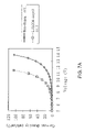
- FIG. 7 a is a plot of current density vs. voltage to show the improvement of an OLED, according to the present invention, over a prior art counterpart.
- FIG. 7 b is a plot of brightness vs. voltage to show the improvement of an OLED, according to the present invention, over a prior art counterpart.
- FIG. 7 c is a plot of luminance yield vs. current density to show the improvement of an OLED, according to the present invention, over a prior art counterpart.
- FIG. 7 d is a plot of power efficiency vs. brightness to show the improvement of an OLED, according to the present invention, over a prior art counterpart.
- FIG. 3 a is a schematic representation showing an embodiment of the present invention.
- an organic optoelectronic device 100 comprises a first electrode 110 , a hole injection layer 120 , a plurality of organic layers 130 , a layer 140 of an oxide-based alkali or alkaline-earth metal intercalation compound and a second electrode 150 .
- the organic layers 130 comprise a hole transport layer, a luminescent layer and an electron transport layer, similar to the organic layers in prior art OLEDs as shown in FIGS. 1 a to 1 c .
- the organic layers 130 may comprise a fullerene layer and a phthalocyanine layer, similar to the organic layers in a prior art photocell, as shown in FIG. 2 .
- the oxide-based alkali or alkaline-earth metal intercalation compound takes the form of a chemical formula A x (M y O z ), where x, y, z are positive integers greater than zero.
- the letter A represents an alkali or alkaline-earth element; M represents a metal, a transitional metal or an alloy thereof; and O represents an oxygen atom.
- the oxide-based alkali or alkaline-earth metal intercalation compound can be: LiMn 2 O 4 , LiCoO 2 , LiNbO 3 , Li 2 WO 4 , Cs 2 WO 4 , CsMnO 4 , CsVO 4 , CsTi 6 O 13 , MgTiO 3 , MgWO 4 , MgZrO 3 , and Li(Ni 0.8 Co 0.2 )O 2 , for example.
- Nb Niobium
- the first electrode 110 is an anode made of any one of the following metallic oxides or the combination thereof: indium-tin oxide, aluminum-doped zinc oxide, indium-doped zinc-oxide, tin-oxide, magnesium-tin oxide, nickel-tungsten oxide, cadmium-tin oxide and the like.
- the second electrode 150 is a cathode that can be made of any one of the following metals or the alloys thereof: aluminum, silver, magnesium-silver alloy and the like.
- buffer layers between the oxide-based alkali or alkaline-earth metal intercalation compound layer 140 and the second electrode layer 150 .
- One or more of these buffer layers can be made of a non-conductive layer having a thickness between 0.3 nm and 5 nm.
- One such buffer layer 146 is shown in FIG. 3 b .
- the buffer layer can also be made of one or more alkali oxides (or halides), alkaline-earth oxides (or halides) having a thickness between 0.3 nm and 5 nm.
- the first electrode 110 is a base electrode (similar to the base electrode 42 of FIG. 2 ) made of any one of the following metallic oxides or the combination thereof: indium-tin oxide, aluminum-doped zinc oxide, indium-doped zinc-oxide, tin-oxide, magnesium-tin oxide, nickel-tungsten oxide, cadmium-tin oxide and the like.
- the second electrode 150 is a top electrode (similar to the top electrode 47 of FIG. 2 ) made of any one of the follow metals or the alloys thereof: aluminum, silver, magnesium-silver alloy and the like.
- buffer layer in the organic light emitting diode it is possible to provide one or more buffer layers 146 between the oxide-based alkali or alkaline-earth metal intercalation compound layer 140 and the top electrode layer of the photocell.
- the present invention provides an electrode structure for use in an organic optoelectronic device.
- the electrode structure 200 comprises a current collector or disperser 150 and an oxide-based alkali or alkaline-earth metal intercalation compound layer 140 associated with the current collector or disperser 150 .
- a non-conductive layer 146 having a thickness substantially between 0.3 nm and 5 nm is provided between the layers 140 and 150 .
- the layer 146 can be made of one or more alkali oxides (or halides), alkaline-earth oxides (or halides).
- the layer 146 is made substantially of LiF.
- the organic layers 130 as shown in FIGS. 3 a and 3 b can have different structures.
- the organic layers comprise a hole transport layer 132 , an emissive layer 134 and an electron transport layer 136 , as shown in FIG. 5 a .
- the organic layers comprise a hole transport layer 132 and a combined ETL/EML layer 135 .
- the combined layer 135 has an electron transport section adjacent to the oxide-based compound layer 140 and an emissive section adjacent to the hole transport layer 132 .
- the organic layers may comprise a hole transport layer 132 , an electron transport 132 and an active layer 133 , as shown in FIG. 5 d .
- the active layer 133 produces electron-hole pairs in response to electromagnetic radiation of in a certain energy range.
- an exemplary OLED is fabricated as shown in FIG. 6 .
- the anode is a 75 nm-thick layer of ITO;
- the hole injection layer is a 15 nm-thick layer of CuPc;
- the hole transport layer is a 60 nm-thick layer of NPB;
- a 75 nm-thick layer of Alq 3 is used both as the luminescent layer and the electronic transport layer;
- the A x (M y O z ) layer is made of LiMn 2 O 4 ;
- the cathode is a 200 nm-thick layer of aluminum.
- the experimental results are shown in FIGS. 7 a to 7 d .
- Curve B represents the device with the LiMn 2 O 4 layer
- Curve A represents the device without the LiMn 2 O 4 layer.
- the present invention provides a method to enhance the operational efficiency in an organic optoelectronic device having an active organic sub-structure disposed between a first electrode and a second electrode.
- the efficiency can be improved by enhancing the election transport process in the organic sub-structure.
- the enhancement can be achieved by providing a layer of one or more oxide-based alkali or alkaline-earth metal intercalation compounds as an efficient electron transport layer to the organic sub-structure.
- the oxide-based alkali or alkaline-earth metal intercalation compound layer is associated with the electrode that is used as a current collector or disperser.
Landscapes
- Physics & Mathematics (AREA)
- Electromagnetism (AREA)
- Electroluminescent Light Sources (AREA)
- Photovoltaic Devices (AREA)
Abstract
Description
-
- x, y, z are positive integers greater than zero;
- A is an element selected from the group consisting of alkali and alkaline-earth element;
- M is an element selected from the group consisting of metals, transitional metals and metallic alloys; and
- O is an oxygen atom.
-
- x, y, z are positive integers greater than zero;
- A is an element selected from
Group 1 andGroup 2 in the Periodic Table of Elements; - M is an element selected from
Group 3 throughGroup 15 in the Period Table of Elements; and - O is an oxygen atom.
-
- a hole transport layer adjacent to the anode,
- an electron transport section adjacent to the inorganic layer; and
- an emissive section between the hole transport layer and the electronic transport section.
-
- x, y, z are positive integers greater than zero;
- A is selected from the group consisting of alkali and alkaline-earth elements;
- M is selected from the group consisting of metals, transitional metals and alloys; and
- O is an oxygen atom.
-
- x, y, z are positive integers greater than zero;
- A is an alkali or alkaline-earth element;
- M is selected from the group consisting of metals, transitional metals and alloys; and
- O is an oxygen atom.
-
- Li=Lithium
- Mn=Manganese
- O=Oxygen
Claims (18)
Priority Applications (5)
| Application Number | Priority Date | Filing Date | Title |
|---|---|---|---|
| US10/995,878 US7259405B2 (en) | 2004-11-23 | 2004-11-23 | Organic photoelectric device with improved electron transport efficiency |
| TW094117788A TWI262740B (en) | 2004-11-23 | 2005-05-31 | Organic photoelectric device with improved electron transport efficiency |
| CNB200510079532XA CN100446634C (en) | 2004-11-23 | 2005-06-23 | Organic photoelectric component, electrode structure used for organic photoelectric component and method for improving operation efficiency of organic photoelectric component |
| JP2005337917A JP4457071B2 (en) | 2004-11-23 | 2005-11-23 | Organic photoelectric conversion device and method for improving operation efficiency of organic photoelectric conversion device |
| US11/726,994 US7528003B2 (en) | 2004-11-23 | 2007-03-22 | Organic photoelectric device with improved electron transport efficiency |
Applications Claiming Priority (1)
| Application Number | Priority Date | Filing Date | Title |
|---|---|---|---|
| US10/995,878 US7259405B2 (en) | 2004-11-23 | 2004-11-23 | Organic photoelectric device with improved electron transport efficiency |
Related Child Applications (1)
| Application Number | Title | Priority Date | Filing Date |
|---|---|---|---|
| US11/726,994 Division US7528003B2 (en) | 2004-11-23 | 2007-03-22 | Organic photoelectric device with improved electron transport efficiency |
Publications (2)
| Publication Number | Publication Date |
|---|---|
| US20060108578A1 US20060108578A1 (en) | 2006-05-25 |
| US7259405B2 true US7259405B2 (en) | 2007-08-21 |
Family
ID=35925101
Family Applications (2)
| Application Number | Title | Priority Date | Filing Date |
|---|---|---|---|
| US10/995,878 Expired - Lifetime US7259405B2 (en) | 2004-11-23 | 2004-11-23 | Organic photoelectric device with improved electron transport efficiency |
| US11/726,994 Expired - Lifetime US7528003B2 (en) | 2004-11-23 | 2007-03-22 | Organic photoelectric device with improved electron transport efficiency |
Family Applications After (1)
| Application Number | Title | Priority Date | Filing Date |
|---|---|---|---|
| US11/726,994 Expired - Lifetime US7528003B2 (en) | 2004-11-23 | 2007-03-22 | Organic photoelectric device with improved electron transport efficiency |
Country Status (4)
| Country | Link |
|---|---|
| US (2) | US7259405B2 (en) |
| JP (1) | JP4457071B2 (en) |
| CN (1) | CN100446634C (en) |
| TW (1) | TWI262740B (en) |
Cited By (4)
| Publication number | Priority date | Publication date | Assignee | Title |
|---|---|---|---|---|
| US20080227357A1 (en) * | 2005-08-10 | 2008-09-18 | Au Optronics Corporation | Organic light-emitting device with improved layer conductivity distribution |
| US20090314350A1 (en) * | 2008-06-18 | 2009-12-24 | Korea Advanced Institute Of Science And Technology | Organic solar cells and method of manufacturing the same |
| US20150295195A1 (en) * | 2012-07-02 | 2015-10-15 | Heliatek Gmbh | Transparent electrode for optoelectronic components |
| US20170062747A1 (en) * | 2015-08-26 | 2017-03-02 | Samsung Electronics Co., Ltd. | Organic photoelectric device and image sensor |
Families Citing this family (36)
| Publication number | Priority date | Publication date | Assignee | Title |
|---|---|---|---|---|
| CN100454603C (en) * | 2005-01-10 | 2009-01-21 | 清华大学 | An organic electroluminescent device |
| JP2007081137A (en) * | 2005-09-14 | 2007-03-29 | Fujifilm Corp | Photoelectric conversion device and solid-state imaging device |
| US7352125B2 (en) * | 2005-12-21 | 2008-04-01 | Lg.Philips Lcd Co., Ltd. | Organic light emitting devices with hole impeding materials |
| CN100444426C (en) * | 2006-04-29 | 2008-12-17 | 中国科学院长春应用化学研究所 | A kind of organic electroluminescence device and preparation method thereof |
| CN101106180B (en) * | 2006-06-08 | 2011-03-16 | 奇美电子股份有限公司 | Image display system |
| DE102007009995A1 (en) * | 2007-03-01 | 2008-09-04 | Hahn-Meitner-Institut Berlin Gmbh | Organic solar cell comprises two electrodes and disposed between photoactive layer having two partial layers, where partial layer emits electrons and later partial layer receives electrons |
| JP4920548B2 (en) * | 2007-10-31 | 2012-04-18 | 株式会社 日立ディスプレイズ | Display device |
| WO2009070534A1 (en) * | 2007-11-28 | 2009-06-04 | Konarka Technologies Gmbh | Organic photovoltaic cells comprising a doped metal oxide buffer layer |
| WO2009110075A1 (en) * | 2008-03-05 | 2009-09-11 | パイオニア株式会社 | Organic semiconductor element |
| JP2009246127A (en) * | 2008-03-31 | 2009-10-22 | Sumitomo Chemical Co Ltd | Organic electroluminescence device and method for manufacturing the same |
| JP5509530B2 (en) * | 2008-03-31 | 2014-06-04 | 住友化学株式会社 | Organic electroluminescence device and method for manufacturing the same |
| EP2180030A3 (en) | 2008-10-23 | 2010-10-06 | National Tsing Hua University | Organic light emitting diode with nano-dots and fabrication method thereof |
| JP5293120B2 (en) * | 2008-11-28 | 2013-09-18 | 住友化学株式会社 | Organic electroluminescence device and method for producing the same |
| CN101419947B (en) * | 2008-12-09 | 2010-06-02 | 河北大学 | A transition metal oxide p-n heterojunction and preparation method thereof |
| EP2256839B1 (en) | 2009-05-28 | 2019-03-27 | IMEC vzw | Single junction or a multijunction photovoltaic cells and method for their fabrication |
| JP2011176305A (en) * | 2010-01-29 | 2011-09-08 | Mitsubishi Chemicals Corp | Photoelectric conversion element, solar cell, and solar cell module |
| JP5934656B2 (en) * | 2010-02-05 | 2016-06-15 | 日東電工株式会社 | Organic light emitting diode with improved efficiency |
| WO2012012136A1 (en) * | 2010-06-30 | 2012-01-26 | First Solar, Inc | Cadmium stannate sputter target |
| TWI437911B (en) * | 2010-08-31 | 2014-05-11 | Nat Univ Tsing Hua | Organic light emitting diode and manufacturing method thereof |
| US9029837B2 (en) * | 2010-10-12 | 2015-05-12 | The Regents Of The University Of Michigan | Photoactive devices including porphyrinoids with coordinating additives |
| CN102810642A (en) * | 2011-06-03 | 2012-12-05 | 海洋王照明科技股份有限公司 | Polymer solar cell and preparation method thereof |
| CN103765621B (en) * | 2011-06-22 | 2017-02-22 | 诺瓦尔德股份有限公司 | Electronic device and compound |
| US9393154B2 (en) | 2011-10-28 | 2016-07-19 | Raymond I Myers | Laser methods for creating an antioxidant sink in the crystalline lens for the maintenance of eye health and physiology and slowing presbyopia development |
| CN103060757B (en) * | 2012-12-14 | 2015-04-01 | 太原理工大学 | Method for Li-doped growth of p-type transparent conductive Ni1-xMgxO crystal film |
| CN106939074B (en) * | 2013-03-08 | 2020-06-16 | 日立化成株式会社 | Treatment liquid containing ionic compound |
| WO2014151655A1 (en) * | 2013-03-15 | 2014-09-25 | Northwestern University | Systems, apparatuses and methods for converting light wavelengths |
| CN103928616B (en) * | 2014-05-04 | 2017-01-25 | 厦门大学 | Application of perovskite oxide SrTiO3 in organic solar cells |
| FR3023064B1 (en) * | 2014-06-25 | 2018-02-02 | Dracula Technologies | PHOTOVOLTAIC DEVICE AND METHOD FOR MANUFACTURING THE SAME |
| KR102263207B1 (en) * | 2014-07-17 | 2021-06-14 | 소니그룹주식회사 | Photoelectric conversion element, image pickup device, optical sensor, and photoelectric conversion element manufacturing method |
| US10254407B2 (en) | 2015-03-02 | 2019-04-09 | Northwestern University | Electroabsorption modulator for depth imaging and other applications |
| EP3168886B8 (en) * | 2015-11-10 | 2023-07-26 | Novaled GmbH | Metallic layer comprising alkali metal and second metal |
| CN105895817B (en) * | 2016-04-11 | 2017-09-01 | 郑州大学 | The perovskite green light LED and preparation method of layer are provided using Ni (Mg) O as hole |
| US11563176B2 (en) * | 2016-12-16 | 2023-01-24 | Nissan Chemical Corporation | Composition for hole collecting layer of organic photoelectric conversion element |
| KR102442210B1 (en) | 2017-12-21 | 2022-09-14 | 삼성디스플레이 주식회사 | Organic electroluminescent device, manufacturing method thereof, and organic electroluminescent display including same |
| EP4012794A1 (en) * | 2020-12-11 | 2022-06-15 | Julius-Maximilians-Universität Würzburg | Emission of electromagnetic radiation and control of properties of the emitted electromagnetic radiation |
| KR20230045947A (en) * | 2021-09-29 | 2023-04-05 | 상라오 징코 솔라 테크놀러지 디벨롭먼트 컴퍼니, 리미티드 | Solar cell and method for manufacturing the same |
Citations (11)
| Publication number | Priority date | Publication date | Assignee | Title |
|---|---|---|---|---|
| US5118986A (en) * | 1989-06-30 | 1992-06-02 | Ricoh Company, Ltd. | Electroluminescent device |
| US5739635A (en) * | 1995-04-27 | 1998-04-14 | Pioneer Electric Corporation | Organic electroluminescent device |
| US6281627B1 (en) * | 1999-01-21 | 2001-08-28 | Tdk Corporation | Organic electroluminescent device with a high resistant inorganic electron injecting layer |
| US20020005696A1 (en) * | 2000-06-13 | 2002-01-17 | Shunpei Yamazaki | Display device |
| US20020155319A1 (en) * | 1999-02-15 | 2002-10-24 | Idemitsu Kosan Co., Ltd. | Organic electroluminescent device and method of manufacture thereof |
| US20030089252A1 (en) * | 2001-11-09 | 2003-05-15 | Sarnecki Greg J. | Production of Electroluminescent Devices |
| US20030170493A1 (en) * | 2002-03-08 | 2003-09-11 | Industrial Technology Research Institute | Photosensitive insulating film of organic light emitting diode (OLED) |
| US20030234609A1 (en) * | 2001-03-08 | 2003-12-25 | Xerox Corporation | Devices with multiple organic-metal mixed layers |
| US20040219389A1 (en) * | 2002-10-28 | 2004-11-04 | Samsung Nec Mobile Display Co., Ltd. | Organic electroluminescence device |
| US20050035430A1 (en) * | 2000-11-28 | 2005-02-17 | Beigel Michael L. | Rectifying charge storage element |
| US20050116240A1 (en) * | 2003-11-26 | 2005-06-02 | Mu-Hyun Kim | Flat panel display |
Family Cites Families (16)
| Publication number | Priority date | Publication date | Assignee | Title |
|---|---|---|---|---|
| US5712504A (en) * | 1995-02-02 | 1998-01-27 | Sumitomo Electric Industries, Ltd. | Pin type light-receiving device, opto electronic conversion circuit, and opto-electronic conversion module |
| US5776623A (en) * | 1996-07-29 | 1998-07-07 | Eastman Kodak Company | Transparent electron-injecting electrode for use in an electroluminescent device |
| JPH10270171A (en) * | 1997-01-27 | 1998-10-09 | Junji Kido | Organic electroluminescent device |
| DE19905694A1 (en) * | 1998-11-27 | 2000-08-17 | Forschungszentrum Juelich Gmbh | Component |
| GB9903251D0 (en) * | 1999-02-12 | 1999-04-07 | Cambridge Display Tech Ltd | Opto-electric devices |
| JP4427838B2 (en) * | 1999-09-09 | 2010-03-10 | ソニー株式会社 | Liquid crystal display |
| JP2001351785A (en) * | 2000-06-09 | 2001-12-21 | Sumitomo Chem Co Ltd | Organic electroluminescence device |
| US6551725B2 (en) * | 2001-02-28 | 2003-04-22 | Eastman Kodak Company | Inorganic buffer structure for organic light-emitting diode devices |
| US6489054B2 (en) | 2001-04-19 | 2002-12-03 | Zinc Matrix Power, Inc. | Battery case with edge seal |
| JP3773423B2 (en) * | 2001-06-11 | 2006-05-10 | Tdk株式会社 | Organic EL device |
| US6580027B2 (en) * | 2001-06-11 | 2003-06-17 | Trustees Of Princeton University | Solar cells using fullerenes |
| US7061175B2 (en) | 2002-08-16 | 2006-06-13 | Universal Display Corporation | Efficiency transparent cathode |
| US6765349B2 (en) * | 2002-09-30 | 2004-07-20 | Eastman Kodak Company | High work function metal alloy cathode used in organic electroluminescent devices |
| JP2004303654A (en) * | 2003-03-31 | 2004-10-28 | Fuji Photo Film Co Ltd | Organic electroluminescent element and its manufacturing method |
| GB0309355D0 (en) * | 2003-04-24 | 2003-06-04 | Univ Cambridge Tech | Organic electronic devices incorporating semiconducting polymer |
| TWI237521B (en) * | 2003-06-27 | 2005-08-01 | Chi Mei Optoelectronics Corp | Organic electro-luminescent device and method of manufacturing the same |
-
2004
- 2004-11-23 US US10/995,878 patent/US7259405B2/en not_active Expired - Lifetime
-
2005
- 2005-05-31 TW TW094117788A patent/TWI262740B/en not_active IP Right Cessation
- 2005-06-23 CN CNB200510079532XA patent/CN100446634C/en not_active Expired - Lifetime
- 2005-11-23 JP JP2005337917A patent/JP4457071B2/en active Active
-
2007
- 2007-03-22 US US11/726,994 patent/US7528003B2/en not_active Expired - Lifetime
Patent Citations (11)
| Publication number | Priority date | Publication date | Assignee | Title |
|---|---|---|---|---|
| US5118986A (en) * | 1989-06-30 | 1992-06-02 | Ricoh Company, Ltd. | Electroluminescent device |
| US5739635A (en) * | 1995-04-27 | 1998-04-14 | Pioneer Electric Corporation | Organic electroluminescent device |
| US6281627B1 (en) * | 1999-01-21 | 2001-08-28 | Tdk Corporation | Organic electroluminescent device with a high resistant inorganic electron injecting layer |
| US20020155319A1 (en) * | 1999-02-15 | 2002-10-24 | Idemitsu Kosan Co., Ltd. | Organic electroluminescent device and method of manufacture thereof |
| US20020005696A1 (en) * | 2000-06-13 | 2002-01-17 | Shunpei Yamazaki | Display device |
| US20050035430A1 (en) * | 2000-11-28 | 2005-02-17 | Beigel Michael L. | Rectifying charge storage element |
| US20030234609A1 (en) * | 2001-03-08 | 2003-12-25 | Xerox Corporation | Devices with multiple organic-metal mixed layers |
| US20030089252A1 (en) * | 2001-11-09 | 2003-05-15 | Sarnecki Greg J. | Production of Electroluminescent Devices |
| US20030170493A1 (en) * | 2002-03-08 | 2003-09-11 | Industrial Technology Research Institute | Photosensitive insulating film of organic light emitting diode (OLED) |
| US20040219389A1 (en) * | 2002-10-28 | 2004-11-04 | Samsung Nec Mobile Display Co., Ltd. | Organic electroluminescence device |
| US20050116240A1 (en) * | 2003-11-26 | 2005-06-02 | Mu-Hyun Kim | Flat panel display |
Non-Patent Citations (1)
| Title |
|---|
| Shinar, Joseph, ED. Organic Light-Emitting Devices: A Survey. AIP Press. New York. 2004. pp. 19-20. * |
Cited By (7)
| Publication number | Priority date | Publication date | Assignee | Title |
|---|---|---|---|---|
| US20080227357A1 (en) * | 2005-08-10 | 2008-09-18 | Au Optronics Corporation | Organic light-emitting device with improved layer conductivity distribution |
| US7816173B2 (en) | 2005-08-10 | 2010-10-19 | Au Optronics Corporation | Organic light-emitting device with improved layer conductivity distribution |
| US20090314350A1 (en) * | 2008-06-18 | 2009-12-24 | Korea Advanced Institute Of Science And Technology | Organic solar cells and method of manufacturing the same |
| US20150295195A1 (en) * | 2012-07-02 | 2015-10-15 | Heliatek Gmbh | Transparent electrode for optoelectronic components |
| US11355719B2 (en) * | 2012-07-02 | 2022-06-07 | Heliatek Gmbh | Transparent electrode for optoelectronic components |
| US20170062747A1 (en) * | 2015-08-26 | 2017-03-02 | Samsung Electronics Co., Ltd. | Organic photoelectric device and image sensor |
| US10403837B2 (en) * | 2015-08-26 | 2019-09-03 | Samsung Electronics Co., Ltd. | Organic photoelectric device and image sensor |
Also Published As
| Publication number | Publication date |
|---|---|
| TWI262740B (en) | 2006-09-21 |
| JP2006148134A (en) | 2006-06-08 |
| US7528003B2 (en) | 2009-05-05 |
| CN100446634C (en) | 2008-12-24 |
| JP4457071B2 (en) | 2010-04-28 |
| US20060108578A1 (en) | 2006-05-25 |
| CN1725915A (en) | 2006-01-25 |
| TW200618664A (en) | 2006-06-01 |
| US20070184575A1 (en) | 2007-08-09 |
Similar Documents
| Publication | Publication Date | Title |
|---|---|---|
| US7528003B2 (en) | Organic photoelectric device with improved electron transport efficiency | |
| US11217764B2 (en) | Organic semiconductor element | |
| US7816173B2 (en) | Organic light-emitting device with improved layer conductivity distribution | |
| US7365360B2 (en) | Organic electronic device | |
| US6875320B2 (en) | Highly transparent top electrode for OLED device | |
| KR101026514B1 (en) | Organic light emitting device | |
| US7074500B2 (en) | Light emitting component comprising organic layers | |
| CN101297018B (en) | Organic electronic device | |
| KR100922760B1 (en) | Organic light emitting device | |
| KR100922755B1 (en) | Organic light emitting device | |
| US20130240847A1 (en) | Monolithic parallel multijunction oled with independent tunable color emission | |
| US6822257B2 (en) | Organic light emitting diode device with organic hole transporting material and phosphorescent material | |
| KR20010092905A (en) | Organic electroluminescent device | |
| KR20140143384A (en) | Metal oxide charge transport material doped with organic molecules | |
| US20120007064A1 (en) | Organic electroluminescent device and method for preparing the same | |
| EP4356448A1 (en) | Sheet resistance component | |
| KR100595928B1 (en) | Organic light emitting device having a light emitting layer of dotted doping structure using a mixed host material | |
| KR101419877B1 (en) | Tandem organic light emitting diodes | |
| WO2022263536A1 (en) | Sheet resistance component | |
| CN104300088A (en) | Organic electroluminescent device and manufacturing method thereof |
Legal Events
| Date | Code | Title | Description |
|---|---|---|---|
| AS | Assignment |
Owner name: AU OPTRONICS CORPORATION, TAIWAN Free format text: ASSIGNMENT OF ASSIGNORS INTEREST;ASSIGNOR:LIU, TSWEN-HSIN;REEL/FRAME:016027/0724 Effective date: 20041119 |
|
| STCF | Information on status: patent grant |
Free format text: PATENTED CASE |
|
| CC | Certificate of correction | ||
| CC | Certificate of correction | ||
| FPAY | Fee payment |
Year of fee payment: 4 |
|
| FPAY | Fee payment |
Year of fee payment: 8 |
|
| MAFP | Maintenance fee payment |
Free format text: PAYMENT OF MAINTENANCE FEE, 12TH YEAR, LARGE ENTITY (ORIGINAL EVENT CODE: M1553); ENTITY STATUS OF PATENT OWNER: LARGE ENTITY Year of fee payment: 12 |
|
| AS | Assignment |
Owner name: AUO CORPORATION, TAIWAN Free format text: CHANGE OF NAME;ASSIGNOR:AU OPTRONICS CORPORATION;REEL/FRAME:063785/0830 Effective date: 20220718 |
|
| AS | Assignment |
Owner name: OPTRONIC SCIENCES LLC, TEXAS Free format text: ASSIGNMENT OF ASSIGNORS INTEREST;ASSIGNOR:AUO CORPORATION;REEL/FRAME:064658/0572 Effective date: 20230802 |