EP1128539B1 - Überspannungsgeschützter Stromwechselrichter mit einem spannungsgesteuerten Schaltkreis - Google Patents
Überspannungsgeschützter Stromwechselrichter mit einem spannungsgesteuerten Schaltkreis Download PDFInfo
- Publication number
- EP1128539B1 EP1128539B1 EP00118908A EP00118908A EP1128539B1 EP 1128539 B1 EP1128539 B1 EP 1128539B1 EP 00118908 A EP00118908 A EP 00118908A EP 00118908 A EP00118908 A EP 00118908A EP 1128539 B1 EP1128539 B1 EP 1128539B1
- Authority
- EP
- European Patent Office
- Prior art keywords
- circuit
- inverter
- diode
- constant voltage
- terminal
- Prior art date
- Legal status (The legal status is an assumption and is not a legal conclusion. Google has not performed a legal analysis and makes no representation as to the accuracy of the status listed.)
- Expired - Lifetime
Links
Images


Classifications
-
- H—ELECTRICITY
- H02—GENERATION; CONVERSION OR DISTRIBUTION OF ELECTRIC POWER
- H02M—APPARATUS FOR CONVERSION BETWEEN AC AND AC, BETWEEN AC AND DC, OR BETWEEN DC AND DC, AND FOR USE WITH MAINS OR SIMILAR POWER SUPPLY SYSTEMS; CONVERSION OF DC OR AC INPUT POWER INTO SURGE OUTPUT POWER; CONTROL OR REGULATION THEREOF
- H02M1/00—Details of apparatus for conversion
- H02M1/32—Means for protecting converters other than automatic disconnection
- H02M1/34—Snubber circuits
-
- H—ELECTRICITY
- H02—GENERATION; CONVERSION OR DISTRIBUTION OF ELECTRIC POWER
- H02M—APPARATUS FOR CONVERSION BETWEEN AC AND AC, BETWEEN AC AND DC, OR BETWEEN DC AND DC, AND FOR USE WITH MAINS OR SIMILAR POWER SUPPLY SYSTEMS; CONVERSION OF DC OR AC INPUT POWER INTO SURGE OUTPUT POWER; CONTROL OR REGULATION THEREOF
- H02M7/00—Conversion of ac power input into dc power output; Conversion of dc power input into ac power output
- H02M7/42—Conversion of dc power input into ac power output without possibility of reversal
- H02M7/44—Conversion of dc power input into ac power output without possibility of reversal by static converters
- H02M7/48—Conversion of dc power input into ac power output without possibility of reversal by static converters using discharge tubes with control electrode or semiconductor devices with control electrode
- H02M7/53—Conversion of dc power input into ac power output without possibility of reversal by static converters using discharge tubes with control electrode or semiconductor devices with control electrode using devices of a triode or transistor type requiring continuous application of a control signal
- H02M7/537—Conversion of dc power input into ac power output without possibility of reversal by static converters using discharge tubes with control electrode or semiconductor devices with control electrode using devices of a triode or transistor type requiring continuous application of a control signal using semiconductor devices only, e.g. single switched pulse inverters
- H02M7/5387—Conversion of dc power input into ac power output without possibility of reversal by static converters using discharge tubes with control electrode or semiconductor devices with control electrode using devices of a triode or transistor type requiring continuous application of a control signal using semiconductor devices only, e.g. single switched pulse inverters in a bridge configuration
-
- H—ELECTRICITY
- H02—GENERATION; CONVERSION OR DISTRIBUTION OF ELECTRIC POWER
- H02M—APPARATUS FOR CONVERSION BETWEEN AC AND AC, BETWEEN AC AND DC, OR BETWEEN DC AND DC, AND FOR USE WITH MAINS OR SIMILAR POWER SUPPLY SYSTEMS; CONVERSION OF DC OR AC INPUT POWER INTO SURGE OUTPUT POWER; CONTROL OR REGULATION THEREOF
- H02M1/00—Details of apparatus for conversion
- H02M1/32—Means for protecting converters other than automatic disconnection
- H02M1/34—Snubber circuits
- H02M1/344—Active dissipative snubbers
-
- H—ELECTRICITY
- H02—GENERATION; CONVERSION OR DISTRIBUTION OF ELECTRIC POWER
- H02M—APPARATUS FOR CONVERSION BETWEEN AC AND AC, BETWEEN AC AND DC, OR BETWEEN DC AND DC, AND FOR USE WITH MAINS OR SIMILAR POWER SUPPLY SYSTEMS; CONVERSION OF DC OR AC INPUT POWER INTO SURGE OUTPUT POWER; CONTROL OR REGULATION THEREOF
- H02M1/00—Details of apparatus for conversion
- H02M1/44—Circuits or arrangements for compensating for electromagnetic interference in converters or inverters
Definitions
- the active clamping circuit overcomes the disadvantage of the above-mentioned snubber circuit and has an advantage that the clamped voltage is kept constant independently of the magnitude of the parasitic inductance and the cut-off current.
- a first problem is that the peak of the surge voltage will exceed a desired clamp voltage. Accordingly, it is necessary to use a switching element having a margin against this clamp voltage and having a higher maximum rated voltage. Since the turn-on resistance of the switching element increases in proportional to the maximum rated voltage, the loss on turning-on increases. Since the switching element having a high maximum rated voltage and a low turn-on resistance has a wider area, it becomes more expensive.
- the capacitor 18 which is connected in parallel with the diode 17 serves to cancel the inductive impedance of the parasitic inductance Lw2. Since the capacitor 18 is connected in series with the parasitic inductance Lw2, appropriate selection of the capacitance of the capacitor 18 depending upon the value of Lw2 causes the negative feedback path to substantially have a resistive impedance to advance the breakdown of the constant voltage diodes 15 and 16. The cancellation or offset effect of the inductive impedance also advances the forward recovery of the diode 17. Since the diode exhibits high impedance until the forward bias becomes about 0.7 volts or more, said feedback path is not formed. However, the recovery to the forward bias conduction is advanced due to the cancellation effect of the inductive impedance.
- a reference Lw3 denotes a parasitic inductance which is the total inductance of the inductances of the respective terminals of the constant voltage diodes 115 and 116 and the diode 117 and the inductance of the wiring which is connected therebetween.
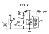
- a reference numeral 110 denotes a radio frequency oscillation absorbing circuit which is connected between the drain and the source of the NMOS transistor.
- the operation of above-mentioned respective circuits is identical to that in Fig. 1.
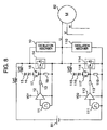
- a circuit which is identical to the above-mentioned circuit is provided for each of the other V and W phases of the three-phase electric motor 82.
- the on-off control signals 11, 111 and relevant on-off control signal for the other phases (phases V and W) are consecutively applied in a predetermined sequence to provide the three-phase electric motor 82 with an a.c. power.
- the present embodiment is substantially identical with the embodiment in Fig. 1 except that the driver 101 has a capability of limiting the output sink current unlike the usual drivers.
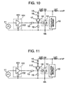
- Embodiments of the driver having a sink current limiting capability are shown in Figs. 13 and 14.
- PMOS 131 and NMOS 132 constitute a common CMOS converter.
- a resistor 133 is connected between the NMOS 132 and a low voltage power source VL.
- a resistor does not act as only an impedance, but gives a negative feedback action on the bias voltage between the gate and the source of the NMOS 132. In other word, stronger negative feedback takes place as higher current flows, resulting in that the resistor will act to suppress the current.
- stronger negative feedback takes place as higher current flows, resulting in that the resistor will act to suppress the current.
- the fourth terminal P4 is led from a connection between the anode of the constant voltage element 1903 and the anode of the diode 1904. Addition of this terminal P4 provides an advantage that the active clamping circuit in the embodiment in Fig. 1 can be formed of only one externally added capacitor. Since the elements 1901 to 1904 are formed on the same semiconductor chip, the inductance which is parasitic to each terminal is very lower than that of conventional discrete part. Accordingly, the capacitance of the external capacitor 1 can be made lower.
Landscapes
- Engineering & Computer Science (AREA)
- Power Engineering (AREA)
- Inverter Devices (AREA)
- Power Conversion In General (AREA)
- Control Of Voltage And Current In General (AREA)
- Electronic Switches (AREA)
Claims (15)
- Wechselrichter mit
einem Hochgeschwindigkeits-Schaltelement (14), um einen Pfad zwischen einem ersten und einem zweiten Anschluß (DD, NN) eines Hauptschaltkreises gemäß einem Signal (11) leitend oder nicht-leitend zu machen, das an einem Ein-Aus-Steueranschluß des Hochgeschwindigkeits-Schaltelements (14) eingegeben wird, und
einer aktiven Klemmschaltung (15 bis 18), die zwischen dem ersten Anschluß (DD) und dem Ein-Aus-Steueranschluß angeordnet ist, wobei die aktive Klemmschaltung eine konstante Spannungsbegrenzungsschaltung (15, 16) und eine parallel angeschlossene Schaltung aufweist, die aus einem Kondensator (18) und einer rückwärts sperrenden Diode (17) gebildet ist, die in Serie mit der konstanten Spannungsbegrenzungsschaltung (15, 16) angeschlossen ist,
dadurch gekennzeichnet, daß die rückwärts sperrende Diode (17) mit ihrer Anode auf der Seite der konstanten Spannungsbegrenzungsschaltung (15, 16) und ihrer Kathode auf der Seite des Ein-Aus-Steueranschlusses angeordnet ist. - Wechselrichter nach Anspruch 1, wobei die rückwärts sperrende Diode (17) eine Grenzschichtdiode oder eine Schottky-Diode ist.
- Wechselrichter nach Anspruch 1, ferner mit einer Schaltung (31) zum Liefern eines in Vorwärtsrichtung fließenden Stroms zu der rückwärts sperrenden Diode (17), wenn das Signal (11) zum Ausschalten des Hochgeschwindigkeits-Schaltelements (14) dient.
- Wechselrichter nach Anspruch 1, ferner mit einer Ansteuerschaltung (101), die eine Senkenstrom-Begrenzungseinrichtung zum Ansteuern des Ein-Aus-Steueranschlusses aufweist.
- Wechselrichter nach Anspruch 4, wobei
die Ansteuerschaltung (101) PMOS- und NMOS-Transistoren (131, 132; 141, 142) aufweist, und
eine Negativfeedback-Impedanzeinrichtung (133) oder ein mit Konstantstrom betriebener Transistor (143) zwischen der Source-Elektrode des NMOS-Transistors (132) und einem Referenzpotential angeordnet ist. - Wechselrichter nach einem der vorstehenden Ansprüche, ferner mit einer Funkfrequenz-Schwingungsabsorptionsschaltung (10), die zwischen dem ersten und dem zweiten Anschluß (DD, NN) des Hochgeschwindigkeits-Schaltelements (14) angeschlossen ist.
- Wechselrichter nach Anspruch 6, wobei die Funkfrequenz-Schwingungsabsorptionsschaltung (10) dazu ausgelegt ist, sowohl eine Spannungsschwingung zu absorbieren, die in Zusammenhang mit einer Negativfeedback-Operation bei einer Überspannungsmitnahme durch die Klemmschaltung (15 bis 18) verursacht ist, als auch eine Spannungsschwingung, die durch parasitäre Resonanz nach der Vollendung der Überspannungsmitnahme entsteht.
- Wechselrichter nach Anspruch 1, wobei der Wechselrichter in einem Überspannungsunterdrückungsystem verwendet wird, das keine Funkfrequenz-Schwingungsabsorptionseinrichtung zwischen dem ersten und dem zweiten Anschluß (DD, NN) des Hochgeschwindigkeits-Schaltelements (14) erfordert.
- Wechselrichter nach einem der vorstehenden Ansprüche, ferner mit
einem zweiten Hochgeschwindigkeits-Schaltelement (114), um einen Pfad zwischen dem zweiten Anschluß (NN) und einem dritten Anschluß eines zweiten Hauptschaltkreises gemäß einem zweiten Signal (111) leitend oder nicht-leitend zu machen, das in einen zweiten Ein-Aus-Steueranschluß des zweiten Hochgeschwindigkeits-Schaltelements (114) eingegeben wird, und
einer zweiten aktiven Klemmschaltung (115 bis 118), die zwischen dem zweiten Anschluß und dem zweiten Ein-Aus-Steueranschluß angeordnet ist und eine zweite konstanten Spannungsbegrenzungsschaltung (115, 116) und eine zweite parallel angeschlossene Schaltung aufweist, die aus einem zweiten Kondensator (118) und einer zweiten rückwärts sperrenden Diode (117) gebildet ist, die in Serie mit der zweiten Spannungsbegrenzungsschaltung (115, 116) angeschlossen ist. - Wechselrichter nach Anspruch 9, ferner mit einer Funkfrequenz-Schwingungsabsorptionsschaltung (901), die aufweist:eine in Serie angeschlossene Schaltung, die aus einem ersten und einem zweiten Kondensator (C1, C2) zwischen dem ersten und dem dritten Anschluß gebildet ist, undeinen Widerstand (RO), der zwischen der Verbindung zwischen dem ersten und dem zweiten Kondensator (C1, C2) und dem zweiten Anschluß angeschlossen ist.
- Wechselrichter nach Anspruch 9, wobei keine Funkfrequenz-Schwingungsabsorptionseinrichtung zwischen dem zweiten und dem dritten Anschluß des zweiten Hochgeschwindigkeits-Schaltelements (114) vorgesehen ist.
- Wechselrichter mit
einem Hochgeschwindigkeits-Schaltelement (14), um einen Pfad zwischen einem ersten und einem zweiten Anschluß (DD, NN) eines Hauptschaltkreises gemäß einem Signal (11) leitend oder nicht-leitend zu machen, das in einem Ein-Aus-Steueranschluß des Hochgeschwindigkeits-Schaltelements (14) eingegeben wird, und
einer aktiven Klemmschaltung (15, 16, 18, 57), die zwischen dem ersten Anschluß (DD) und dem Ein-Aus-Steueranschluß angeordnet ist, wobei die aktive Klemmschaltung eine konstante Spannungsbegrenzungsschaltung (15, 16) und eine parallel angeschlossene Schaltung (18, 57) aufweist, wobei die parallel angeschlossene Schaltung in Serie mit der konstanten Spannungsbegrenzungsschaltung (15, 16) angeschlossen ist und einen Kondensator (18) aufweist,
dadurch gekennzeichnet, daß die parallel angeschlossene Schaltung ferner einen Feldeffekttransistor (57) aufweist, der parallel zu dem Kondensator (18) angeschlossen und dazu ausgelegt ist, sich selbst einzuschalten, wenn das Signal (11) das Hochgeschwindigkeits-Schaltelement (14) ausschaltet. - Wechselrichter nach einem der vorstehenden Ansprüche, wobei die konstante Spannungsbegrenzungsschaltung (15, 16) eine Konstantspannungsdiode aufweist, deren Anode auf der Seite der parallel angeschlossenen Schaltung angeordnet ist, und deren Kathode auf der Seite des ersten Anschlusses (DD) angeordnet ist.
- Wechselrichter nach einem der vorstehenden Ansprüche, wobei die konstante Spannungsbegrenzungsschaltung (15, 16) einen bipolaren Transistor (QN), wenigstens eine Zener-Diode (ZD) und zwei Widerstände (R1, R2) aufweist.
- Wechselrichter nach Anspruch 1, gebildet durch eine als Wechselrichtereinheit (1900) betriebenes Halbleiterbauelement mit einem zusätzlichen Anschluß (P4), der zwischen der rückwärts sperrenden Diode (1904) und der konstanten Spannungsbegrenzungsschaltung (1902, 1903) angeordnet ist, wobei die parallel angeschlossene Schaltung durch Anschließen eines externen Kondensators zwischen dem Ein-Aus-Steueranschluß (P3) und dem zusätzlichen Anschluß (P4) gebildet ist.
Applications Claiming Priority (2)
| Application Number | Priority Date | Filing Date | Title |
|---|---|---|---|
| JP2000055954 | 2000-02-28 | ||
| JP2000055954A JP3598933B2 (ja) | 2000-02-28 | 2000-02-28 | 電力変換装置 |
Publications (3)
| Publication Number | Publication Date |
|---|---|
| EP1128539A2 EP1128539A2 (de) | 2001-08-29 |
| EP1128539A3 EP1128539A3 (de) | 2003-07-23 |
| EP1128539B1 true EP1128539B1 (de) | 2006-04-26 |
Family
ID=18576992
Family Applications (1)
| Application Number | Title | Priority Date | Filing Date |
|---|---|---|---|
| EP00118908A Expired - Lifetime EP1128539B1 (de) | 2000-02-28 | 2000-08-31 | Überspannungsgeschützter Stromwechselrichter mit einem spannungsgesteuerten Schaltkreis |
Country Status (4)
| Country | Link |
|---|---|
| US (1) | US6373731B1 (de) |
| EP (1) | EP1128539B1 (de) |
| JP (1) | JP3598933B2 (de) |
| DE (1) | DE60027538T2 (de) |
Families Citing this family (46)
| Publication number | Priority date | Publication date | Assignee | Title |
|---|---|---|---|---|
| JP3812353B2 (ja) * | 2001-03-19 | 2006-08-23 | 株式会社日立製作所 | 半導体電力変換装置 |
| DE10231198A1 (de) * | 2002-07-10 | 2004-01-29 | eupec Europäische Gesellschaft für Leistungshalbleiter mbH | Verfahren und Schaltungsanordnung zum Begrenzen einer Überspannung |
| JP4359250B2 (ja) | 2005-02-10 | 2009-11-04 | 株式会社日立製作所 | インターフェース回路及び電力変換装置並びに車載用電機システム |
| US20060214704A1 (en) * | 2005-03-24 | 2006-09-28 | Nec Electronics Corporation | Load drive circuit |
| EP1748539B1 (de) * | 2005-07-29 | 2018-06-06 | TDK Corporation | Schaltnetzteil mit Überspannungsunterdrückung |
| JP4343897B2 (ja) | 2005-12-12 | 2009-10-14 | 三菱電機株式会社 | 電力変換装置 |
| JP4432953B2 (ja) * | 2006-09-27 | 2010-03-17 | 株式会社日立製作所 | 半導体電力変換装置 |
| US8369109B2 (en) * | 2006-11-09 | 2013-02-05 | Osram Gesellschaft Mit Beschrankter Haftung | Self-oscillating bipolar transistor DC/AC/DC converter using a pulse forming timer |
| US20080123239A1 (en) * | 2006-11-28 | 2008-05-29 | Emerson Electric Co. | Transient voltage surge suppressor |
| JP2009011013A (ja) * | 2007-06-26 | 2009-01-15 | Hitachi Ltd | 電力変換装置 |
| JP4333802B1 (ja) | 2008-03-18 | 2009-09-16 | トヨタ自動車株式会社 | インバータの駆動装置 |
| JP5157011B2 (ja) * | 2008-04-28 | 2013-03-06 | 株式会社小松製作所 | スイッチング装置のサージ電圧抑制回路 |
| JP4992876B2 (ja) * | 2008-09-30 | 2012-08-08 | 三菱電機株式会社 | インバータ装置 |
| KR101014152B1 (ko) | 2008-10-15 | 2011-02-14 | 기아자동차주식회사 | 차량 인버터 회로 및 그를 이용한 차량 |
| JP5309923B2 (ja) * | 2008-11-21 | 2013-10-09 | 富士電機株式会社 | 半導体素子の駆動回路 |
| JP5287294B2 (ja) * | 2009-01-28 | 2013-09-11 | 富士電機株式会社 | 半導体保護回路 |
| US7990743B2 (en) * | 2009-10-20 | 2011-08-02 | General Electric Company | System and method for decreasing solar collector system losses |
| US7855906B2 (en) * | 2009-10-26 | 2010-12-21 | General Electric Company | DC bus voltage control for two stage solar converter |
| DE102009046615A1 (de) * | 2009-11-11 | 2011-05-19 | Zf Friedrichshafen Ag | Leistungsschalteranordnung für einen Wechselrichter |
| EP2518885B1 (de) * | 2009-12-24 | 2017-07-05 | Panasonic Corporation | Stromumrichter mit halbleiterschaltelement |
| US8050062B2 (en) * | 2010-02-24 | 2011-11-01 | General Electric Company | Method and system to allow for high DC source voltage with lower DC link voltage in a two stage power converter |
| JP5682269B2 (ja) | 2010-12-06 | 2015-03-11 | サンケン電気株式会社 | ゲート駆動回路及び半導体装置 |
| US8441770B2 (en) * | 2011-02-18 | 2013-05-14 | ETA Semiconductor Inc | Voltage spikes control for power converters |
| JP5344005B2 (ja) * | 2011-06-07 | 2013-11-20 | 株式会社豊田自動織機 | スイッチング回路 |
| IN2014DN03024A (de) | 2011-12-07 | 2015-05-08 | Tm4 Inc | |
| AT512623B1 (de) * | 2012-03-06 | 2016-07-15 | Felix Dipl Ing Dr Himmelstoss | Spannungsbegrenzer mit Rückspeisung |
| CN102611288B (zh) * | 2012-03-19 | 2014-05-14 | 南京航空航天大学 | 氮化镓功率晶体管三电平驱动方法 |
| JP5796599B2 (ja) * | 2013-05-23 | 2015-10-21 | 株式会社デンソー | 半導体モジュールおよびスイッチング素子の駆動装置 |
| US8847656B1 (en) * | 2013-07-03 | 2014-09-30 | Honeywell International Inc. | Approach for driving multiple MOSFETs in parallel for high power solid state power controller applications |
| JP6129677B2 (ja) * | 2013-08-05 | 2017-05-17 | 日立オートモティブシステムズ株式会社 | 電動モータの駆動制御装置 |
| DE102013219670A1 (de) * | 2013-09-30 | 2015-04-02 | Robert Bosch Gmbh | Inverterschaltung |
| JP6156073B2 (ja) | 2013-11-08 | 2017-07-05 | 株式会社明電舎 | 半導体スイッチング素子の保護回路および電力変換装置 |
| JP6255997B2 (ja) * | 2013-12-27 | 2018-01-10 | 富士通株式会社 | 半導体装置 |
| DE112014006953T5 (de) * | 2014-09-11 | 2017-06-08 | Mitsubishi Electric Corporation | Halbleitervorrichtung |
| JP6371739B2 (ja) * | 2015-08-05 | 2018-08-08 | 日立オートモティブシステムズ株式会社 | 誘導性負荷駆動装置 |
| DE102015118165A1 (de) * | 2015-10-23 | 2017-04-27 | Infineon Technologies Ag | Elektrische baugruppe, umfassend eine halbleiterschaltvorrichtung und eine klemmdiode |
| DE102015013875B4 (de) | 2015-10-28 | 2022-05-05 | Audi Ag | Wechselrichter für eine elektrische Maschine, elektrische Antriebseinrichtung für ein Kraftfahrzeug sowie Verfahren zum Betreiben eines Wechselrichters |
| CN107332543A (zh) * | 2016-04-28 | 2017-11-07 | 中兴通讯股份有限公司 | 一种电子接触器的保护电路及系统 |
| FR3051301B1 (fr) * | 2016-05-11 | 2019-06-28 | Valeo Systemes De Controle Moteur | Circuit de limitation de tension, systeme d'interrupteur et convertisseur electrique |
| JP2017208988A (ja) * | 2016-05-20 | 2017-11-24 | 新電元工業株式会社 | スイッチング電源装置及びクランプ型半導体装置 |
| JP6173528B1 (ja) | 2016-06-02 | 2017-08-02 | 三菱電機株式会社 | 電力変換器 |
| JP6757637B2 (ja) * | 2016-09-23 | 2020-09-23 | 株式会社ケーヒン | 誘導性負荷駆動装置 |
| DE102017219499A1 (de) * | 2017-11-02 | 2019-05-02 | Siemens Aktiengesellschaft | Elektrische Anordnung mit Teilmodulen sowie Teilmodule als solche |
| US10277107B1 (en) * | 2017-12-27 | 2019-04-30 | Stmicroelectronics S.R.L. | Synchronous rectifier gate driver with active clamp |
| WO2021028330A1 (en) * | 2019-08-12 | 2021-02-18 | Signify Holding B.V. | Mosfet circuit, for example for use in a tapped linear driver, and surge protection method |
| CN116131581B (zh) * | 2023-04-17 | 2023-07-04 | 湖南大学 | 集成振荡抑制电路的功率模块及方法 |
Family Cites Families (17)
| Publication number | Priority date | Publication date | Assignee | Title |
|---|---|---|---|---|
| JPS59201676A (ja) * | 1983-04-28 | 1984-11-15 | Canon Inc | フライバックトランスを用いた電源装置 |
| JPH0785661B2 (ja) * | 1985-04-19 | 1995-09-13 | 松下電工株式会社 | インバ−タ装置 |
| JPH078143B2 (ja) * | 1985-12-23 | 1995-01-30 | 松下電工株式会社 | インバ−タ装置 |
| JPS63114315A (ja) * | 1986-10-30 | 1988-05-19 | Nec Corp | 直流クランプ回路 |
| JPH02298067A (ja) * | 1989-05-12 | 1990-12-10 | Nec Corp | コレクタクランプ回路 |
| JPH0575439A (ja) * | 1991-09-11 | 1993-03-26 | Nec Corp | Ttl回路 |
| JPH05251970A (ja) * | 1992-03-04 | 1993-09-28 | Yokogawa Electric Corp | クランプ回路 |
| JPH06326579A (ja) * | 1993-05-12 | 1994-11-25 | Tokai Rika Co Ltd | Mos−fet を用いた負荷駆動回路 |
| JP2957407B2 (ja) * | 1994-01-24 | 1999-10-04 | 三菱電機株式会社 | 3レベルインバータ装置 |
| JP3193827B2 (ja) * | 1994-04-28 | 2001-07-30 | 三菱電機株式会社 | 半導体パワーモジュールおよび電力変換装置 |
| JP3428154B2 (ja) * | 1994-07-14 | 2003-07-22 | 浜松ホトニクス株式会社 | 同期検出回路 |
| JPH08214545A (ja) * | 1995-01-31 | 1996-08-20 | Nippon Steel Corp | スイッチング電力変換装置 |
| SE9500761D0 (sv) * | 1995-03-02 | 1995-03-02 | Abb Research Ltd | Skyddskrets för seriekopplade krafthalvledare |
| JPH09139660A (ja) * | 1995-11-16 | 1997-05-27 | Mitsubishi Electric Corp | 半導体スイッチ回路 |
| JP3632385B2 (ja) * | 1997-07-30 | 2005-03-23 | 株式会社デンソー | 誘導性負荷の駆動回路 |
| DE19740540C1 (de) * | 1997-09-15 | 1999-03-18 | Siemens Ag | Schaltungsanordnung zur Begrenzung von Überspannungen bei Leistungshalbleitern |
| JP3539194B2 (ja) * | 1998-03-10 | 2004-07-07 | 日産自動車株式会社 | パワーmosfet回路 |
-
2000
- 2000-02-28 JP JP2000055954A patent/JP3598933B2/ja not_active Expired - Lifetime
- 2000-08-31 EP EP00118908A patent/EP1128539B1/de not_active Expired - Lifetime
- 2000-08-31 DE DE60027538T patent/DE60027538T2/de not_active Expired - Lifetime
- 2000-09-01 US US09/654,084 patent/US6373731B1/en not_active Expired - Lifetime
Also Published As
| Publication number | Publication date |
|---|---|
| JP2001245466A (ja) | 2001-09-07 |
| EP1128539A2 (de) | 2001-08-29 |
| EP1128539A3 (de) | 2003-07-23 |
| JP3598933B2 (ja) | 2004-12-08 |
| DE60027538D1 (de) | 2006-06-01 |
| US6373731B1 (en) | 2002-04-16 |
| DE60027538T2 (de) | 2006-12-07 |
Similar Documents
| Publication | Publication Date | Title |
|---|---|---|
| EP1128539B1 (de) | Überspannungsgeschützter Stromwechselrichter mit einem spannungsgesteuerten Schaltkreis | |
| US7315439B2 (en) | Method and circuit arrangement for limiting an overvoltage | |
| US6407937B2 (en) | Active overvoltage protection apparatus for a bidirectional power switch in common collector mode | |
| US5107151A (en) | Switching circuit employing electronic devices in series with an inductor to avoid commutation breakdown and extending the current range of switching circuits by using igbt devices in place of mosfets | |
| US6054890A (en) | Electronic switching circuit with reduction of switching transients | |
| US6094087A (en) | Gate drive circuit for isolated gate devices and method of operation thereof | |
| US20130021067A1 (en) | Method for driving igbt | |
| JP5499855B2 (ja) | 電圧駆動素子の駆動回路 | |
| US5822199A (en) | Controller for a power switch and method of operation thereof | |
| US7701279B2 (en) | Driving circuit for an emitter-switching configuration | |
| US5650906A (en) | Circuit arrangement for protecting power semiconductor switches which can be switched on and off against overvoltages | |
| US11539361B2 (en) | Semiconductor device signal transmission circuit for drive-control, method of controlling semiconductor device signal transmission circuit for drive-control, semiconductor device, power conversion device, and electric system for railway vehicle | |
| US6438002B2 (en) | Active snubber circuit with controllable DV/DT | |
| EP1178596B1 (de) | Wechselrichtervorrichtung | |
| US6680630B1 (en) | Driver circuit for power device | |
| JP4110052B2 (ja) | インバータ回路 | |
| Rodrigues et al. | Economical methods for SiC JFET’s short-circuit protection using commercial gate drivers | |
| WO2019163114A1 (ja) | パワーモジュール及びスイッチング電源 | |
| EP0475704A1 (de) | Antriebsschaltkreis für einen elektrischen Motor | |
| EP0920114A1 (de) | Stromwandler mit mos-gate-halbleiteranordnung | |
| US20230012109A1 (en) | Over-voltage protection circuitry | |
| Tang et al. | Passive resonant level shifter for suppression of crosstalk effect and reduction of body-diode loss in SiC-based bridge leg | |
| JP2023028645A (ja) | パワー半導体モジュール、並びにそれを用いたモータ駆動システム | |
| JPH0951068A (ja) | 半導体装置 | |
| Ziemba et al. | Efficient IGBT switching |
Legal Events
| Date | Code | Title | Description |
|---|---|---|---|
| PUAI | Public reference made under article 153(3) epc to a published international application that has entered the european phase |
Free format text: ORIGINAL CODE: 0009012 |
|
| AK | Designated contracting states |
Kind code of ref document: A2 Designated state(s): AT BE CH CY DE DK ES FI FR GB GR IE IT LI LU MC NL PT SE |
|
| AX | Request for extension of the european patent |
Free format text: AL;LT;LV;MK;RO;SI |
|
| PUAL | Search report despatched |
Free format text: ORIGINAL CODE: 0009013 |
|
| AK | Designated contracting states |
Designated state(s): AT BE CH CY DE DK ES FI FR GB GR IE IT LI LU MC NL PT SE |
|
| AX | Request for extension of the european patent |
Extension state: AL LT LV MK RO SI |
|
| RIC1 | Information provided on ipc code assigned before grant |
Ipc: 7H 02M 1/00 B Ipc: 7H 02M 7/538 A |
|
| 17P | Request for examination filed |
Effective date: 20040120 |
|
| AKX | Designation fees paid |
Designated state(s): DE FR IT |
|
| 17Q | First examination report despatched |
Effective date: 20040331 |
|
| GRAP | Despatch of communication of intention to grant a patent |
Free format text: ORIGINAL CODE: EPIDOSNIGR1 |
|
| GRAS | Grant fee paid |
Free format text: ORIGINAL CODE: EPIDOSNIGR3 |
|
| GRAA | (expected) grant |
Free format text: ORIGINAL CODE: 0009210 |
|
| AK | Designated contracting states |
Kind code of ref document: B1 Designated state(s): DE FR IT |
|
| REF | Corresponds to: |
Ref document number: 60027538 Country of ref document: DE Date of ref document: 20060601 Kind code of ref document: P |
|
| ET | Fr: translation filed | ||
| PLBE | No opposition filed within time limit |
Free format text: ORIGINAL CODE: 0009261 |
|
| STAA | Information on the status of an ep patent application or granted ep patent |
Free format text: STATUS: NO OPPOSITION FILED WITHIN TIME LIMIT |
|
| 26N | No opposition filed |
Effective date: 20070129 |
|
| PGFP | Annual fee paid to national office [announced via postgrant information from national office to epo] |
Ref country code: FR Payment date: 20130808 Year of fee payment: 14 |
|
| PGFP | Annual fee paid to national office [announced via postgrant information from national office to epo] |
Ref country code: IT Payment date: 20130819 Year of fee payment: 14 |
|
| PG25 | Lapsed in a contracting state [announced via postgrant information from national office to epo] |
Ref country code: IT Free format text: LAPSE BECAUSE OF NON-PAYMENT OF DUE FEES Effective date: 20140831 |
|
| REG | Reference to a national code |
Ref country code: FR Ref legal event code: ST Effective date: 20150430 |
|
| PG25 | Lapsed in a contracting state [announced via postgrant information from national office to epo] |
Ref country code: FR Free format text: LAPSE BECAUSE OF NON-PAYMENT OF DUE FEES Effective date: 20140901 |
|
| PGFP | Annual fee paid to national office [announced via postgrant information from national office to epo] |
Ref country code: DE Payment date: 20190820 Year of fee payment: 20 |
|
| REG | Reference to a national code |
Ref country code: DE Ref legal event code: R071 Ref document number: 60027538 Country of ref document: DE |