EP1128539A2 - Uberspannungsgeschützter Stromwechselrichter mit einem spannungsgesteuerten Schaltkreis - Google Patents
Uberspannungsgeschützter Stromwechselrichter mit einem spannungsgesteuerten Schaltkreis Download PDFInfo
- Publication number
- EP1128539A2 EP1128539A2 EP00118908A EP00118908A EP1128539A2 EP 1128539 A2 EP1128539 A2 EP 1128539A2 EP 00118908 A EP00118908 A EP 00118908A EP 00118908 A EP00118908 A EP 00118908A EP 1128539 A2 EP1128539 A2 EP 1128539A2
- Authority
- EP
- European Patent Office
- Prior art keywords
- circuit
- switching element
- control terminal
- conducting
- terminal
- Prior art date
- Legal status (The legal status is an assumption and is not a legal conclusion. Google has not performed a legal analysis and makes no representation as to the accuracy of the status listed.)
- Granted
Links
Images


Classifications
-
- H—ELECTRICITY
- H02—GENERATION; CONVERSION OR DISTRIBUTION OF ELECTRIC POWER
- H02M—APPARATUS FOR CONVERSION BETWEEN AC AND AC, BETWEEN AC AND DC, OR BETWEEN DC AND DC, AND FOR USE WITH MAINS OR SIMILAR POWER SUPPLY SYSTEMS; CONVERSION OF DC OR AC INPUT POWER INTO SURGE OUTPUT POWER; CONTROL OR REGULATION THEREOF
- H02M1/00—Details of apparatus for conversion
- H02M1/32—Means for protecting converters other than automatic disconnection
- H02M1/34—Snubber circuits
-
- H—ELECTRICITY
- H02—GENERATION; CONVERSION OR DISTRIBUTION OF ELECTRIC POWER
- H02M—APPARATUS FOR CONVERSION BETWEEN AC AND AC, BETWEEN AC AND DC, OR BETWEEN DC AND DC, AND FOR USE WITH MAINS OR SIMILAR POWER SUPPLY SYSTEMS; CONVERSION OF DC OR AC INPUT POWER INTO SURGE OUTPUT POWER; CONTROL OR REGULATION THEREOF
- H02M7/00—Conversion of ac power input into dc power output; Conversion of dc power input into ac power output
- H02M7/42—Conversion of dc power input into ac power output without possibility of reversal
- H02M7/44—Conversion of dc power input into ac power output without possibility of reversal by static converters
- H02M7/48—Conversion of dc power input into ac power output without possibility of reversal by static converters using discharge tubes with control electrode or semiconductor devices with control electrode
- H02M7/53—Conversion of dc power input into ac power output without possibility of reversal by static converters using discharge tubes with control electrode or semiconductor devices with control electrode using devices of a triode or transistor type requiring continuous application of a control signal
- H02M7/537—Conversion of dc power input into ac power output without possibility of reversal by static converters using discharge tubes with control electrode or semiconductor devices with control electrode using devices of a triode or transistor type requiring continuous application of a control signal using semiconductor devices only, e.g. single switched pulse inverters
- H02M7/5387—Conversion of dc power input into ac power output without possibility of reversal by static converters using discharge tubes with control electrode or semiconductor devices with control electrode using devices of a triode or transistor type requiring continuous application of a control signal using semiconductor devices only, e.g. single switched pulse inverters in a bridge configuration
-
- H—ELECTRICITY
- H02—GENERATION; CONVERSION OR DISTRIBUTION OF ELECTRIC POWER
- H02M—APPARATUS FOR CONVERSION BETWEEN AC AND AC, BETWEEN AC AND DC, OR BETWEEN DC AND DC, AND FOR USE WITH MAINS OR SIMILAR POWER SUPPLY SYSTEMS; CONVERSION OF DC OR AC INPUT POWER INTO SURGE OUTPUT POWER; CONTROL OR REGULATION THEREOF
- H02M1/00—Details of apparatus for conversion
- H02M1/32—Means for protecting converters other than automatic disconnection
- H02M1/34—Snubber circuits
- H02M1/344—Active dissipative snubbers
-
- H—ELECTRICITY
- H02—GENERATION; CONVERSION OR DISTRIBUTION OF ELECTRIC POWER
- H02M—APPARATUS FOR CONVERSION BETWEEN AC AND AC, BETWEEN AC AND DC, OR BETWEEN DC AND DC, AND FOR USE WITH MAINS OR SIMILAR POWER SUPPLY SYSTEMS; CONVERSION OF DC OR AC INPUT POWER INTO SURGE OUTPUT POWER; CONTROL OR REGULATION THEREOF
- H02M1/00—Details of apparatus for conversion
- H02M1/44—Circuits or arrangements for compensating for electromagnetic interference in converters or inverters
Definitions
- the present invention relates to a surge voltage suppressed power inverter using a voltage driven switching element such as a MOS transistor and the like.
- IGBTs or MOSFETs which can be switched at high speeds have been used as switching elements for the power inverter.
- JP-A-9-139660 An example of prior art surge voltage suppressing means is described in JP-A-9-139660.
- a series circuit of a capacitor and resistor is connected between the collector and emitter of an IGBT in parallel.
- a diode is connected in parallel with the resister.
- This circuit is referred to as a "snubber circuit". Since the circuit is arranged to absorb surge voltage per se by the capacitor, there occurs problem as follows: Firstly, since the capacitor will have higher impedance at low frequencies, sufficient surge suppression is not attained for a surge voltage having a wide time width.
- JP-A-6-32657 Another example of the prior art surge voltage suppressing means is disclosed in JP-A-6-326579. Since a surge voltage which is generated at the drain terminal of a MOS transistor is clamped at a given voltage in present means, a series-connected circuit of a zener-diode and a reverse blocking diode is connected between the gate and the drain of the MOS transistor. When a current flowing through a load is cut off by driving the MOSFET into an non-conductive state, a surge voltage is generated on the drain terminal due to the parasitic inductance. When the surge voltage will exceed the sum of the breakdown voltage and the forward voltage of the zener diode, the voltage on the gate of the MOS transistor will become higher, so that the MOS transistor is turned on to absorb the surge voltage.
- the active clamping circuit overcomes the disadvantage of the above-mentioned snubber circuit and has an advantage that the clamped voltage is kept constant independently of the magnitude of the parasitic inductance and the cut-off current.
- a first problem is that the peak of the surge voltage will exceed a desired clamp voltage. Accordingly, it is necessary to use a switching element having a margin against this clamp voltage and having a higher maximum rated voltage. Since the turn-on resistance of the switching element increases in proportional to the maximum rated voltage, the loss on turning-on increases. Since the switching element having a high maximum rated voltage and a low turn-on resistance has a wider area, it becomes more expensive.
- a second problem is voltage oscillation P2 at radio frequencies during the clamping operation and the voltage oscillation at radio frequencies P3 after the completion of the clamping operation (see Fig. 18). Although this oscillation will not cause the breakdown of the switching element due to the surge voltage, there is a risk of causing electromagnetic interference (EMI) noise which may adversely affect to peripheral electronic circuits and devices.
- EMI electromagnetic interference
- the present inventors have found that the reason why the peak voltage can not be clamped at a desired voltage is that the formation of a negative feedback path between the drain and the gate of an MOS transistor has a time lag when a surge-voltage occurs.
- the time lag is caused mainly by an increase in the radio frequency impedance due to the parasitic inductance in the negative feedback path and the time lag due to the forward recovery time of the reverse-blocking diode.
- the voltage swinging is a loop oscillation which is inherent in the negative feedback control, that is a resonant oscillation caused by the parasitic inductance and parasitic capacitance.
- a power inverter comprises a circuit for canceling an inductive impedance of a negative feedback path as means for speeding up the negative feedback path extending from the drain of a MOS switching element to the gate thereof and a circuit for shortening the forward recovery period of time of a reverse-blocking diode in the negative feedback path.
- the power inverter further comprises a circuit for preventing the radio frequency oscillation after the suppression of the surge voltage.
- Fig. 1 is a circuit diagram of a power converter showing a first embodiment of the present invention.
- Fig. 2 is a circuit diagram of a power converter showing a second embodiment of the present invention.
- Fig. 3 is a circuit diagram of a power converter showing a third embodiment of the present invention.
- Fig. 4 is a circuit diagram of a power converter showing a fourth embodiment of the present invention.
- Fig. 5 is a circuit diagram of a power converter showing a fifth embodiment of the present invention.
- Fig. 6 is a circuit diagram of a power converter showing a sixth embodiment of the present invention.
- Fig. 7 is a circuit diagram of a power converter showing a seventh embodiment of the present invention.
- Fig. 8 is a circuit diagram of a power converter showing an eighth embodiment of the present invention.
- Fig. 9 is a circuit diagram of a power converter showing a ninth embodiment of the present invention.
- Fig. 10 is a circuit diagram of a power converter showing a tenth embodiment of the present invention.
- Fig. 11 is a circuit diagram of a power converter showing an eleventh embodiment of the present invention.
- Fig. 12 is a waveform view explaining the time lag of the negative feedback path.
- Fig. 13 is a circuit diagram showing an example of a driver circuit capable of limiting a sink current, which is used in the present invention.
- Fig. 14 is a circuit diagram showing another example of a driver circuit capable of limiting a sink current, which is used in the present invention.
- Fig. 15 is a circuit diagram showing another voltage limiting circuit which is used in the present invention.
- Fig. 16 is a circuit diagram showing an example of a radio frequency oscillation absorbing circuit which is used in the present invention.
- Fig. 17 is a circuit diagram showing another example of a radio frequency oscillation absorbing circuit which is used in the present invention.
- Fig. 18 is a waveform view showing the switching voltage in the present invention.
- Fig. 19 is a circuit diagram of a power converter showing a twelfth embodiment of the present invention.
- Fig. 20 is a circuit diagram showing an example in which the present invention is applied to a three-phase inverter.
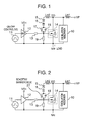
- FIG. 1 A first embodiment of the present invention is illustrated in Fig. 1. Like elements and like components are designated by like numerals in the following description.
- reference numerals 11, 12, 13 and 14 denote an on-off control signal, driver, resister and NMOS transistor, respectively.
- the output of the driver 12 is connected to the gate of the NMOS transistor 14 via the resister 13.
- Reference numerals 14 and 15 denote series-connected constant voltage diodes, each having a cathode connected to the drain of the NMOS transistor 14.
- a diode 17 has its anode and cathode which are connected to the anode of the constant voltage diode 16 and the gate of the NMOS transistor 14, respectively.
- a reference Lwl denotes a parasitic inductance of the wiring of a power source (supply) VP and Lw2 denotes a parasitic inductance which is the total inductance of the inductances of the respective terminals of the constant voltage diodes 15 and 16 and the diode 17 and the inductance of the wiring which is connected therebetween.
- a reference numeral 10 denotes a radio frequency oscillation absorbing circuit which is connected between the drain and the source of the NMOS transistor.
- this power inverter circuit When the on-off control signal 11 instructs the turn-on, a high level signal is applied to the gate of the NMOS transistor via the driver 12, so that the NMOS transistor 14 is tuned on. As a result, a current i is supplied to a load (not shown) from the power source VP via the parasitic inductance Lwl and the NMOS transistor 14. At this time, an electric energy Lw1 x i x i/2 is stored in the parasitic inductor Lw1. Since a node DD is at a low potential when the NMOS transistor 14 is conductive, a negative feedback path including series connected constant voltage diodes 15, 16 and the diode 17 is opened due to the fact that the diode 17 is reverse-biased.
- the capacitor 18 which is connected in parallel with the diode 17 serves to cancel the inductive impedance of the parasitic inductance Lw2. Since the capacitor 18 is connected in series with the parasitic inductance Lw2, appropriate selection of the capacitance of the capacitor 18 depending upon the value of Lw2 causes the negative feedback path to substantially have a resistive impedance to advance the breakdown of the constant voltage diodes 15 and 16. The cancellation or offset effect of the inductive impedance also advances the forward recovery of the diode 17. Since the diode exhibits high impedance until the forward bias becomes about 0.7 volts or more, said feedback path is not formed. However, the recovery to the forward bias conduction is advanced due to the cancellation effect of the inductive impedance.
- Fig. 12 shows the changes in the current flowing through the negative feedback path when a surge voltage is generated.
- References A and B denote currents flowing through the capacitor 18 and the diode 17, respectively.
- the negative feedback path is formed since the time t0 if the capacitor 18 is provided. The formation of the negative feedback path is delayed from time t0 to time tl.
- the lag of the formation of the negative feedback path due to the presence of the parasitic inductance Lw2 is remarkably improved in the present embodiment.
- the negative feedback path is quickly formed against the kickback voltage having high dv/dt.
- Conventional high peak voltage is improved so that it is placed to a lower voltage as shown as the peak voltage in Fig. 18.
- a reference numeral 10 denotes a radio frequency oscillation absorbing circuit which is connected between the nodes on the sides of the drain and the source of the NMOS transistor 14.
- the absorbing circuit may comprise a series circuit of a capacitor and a resister as shown in Fig. 16 or a circuit of only one capacitor.
- the role of the oscillation absorbing circuit is to absorb both the radio frequency oscillation due to the negative feedback operation on generation of the surge voltage and the radio frequency oscillation caused by Lwl and the parasitic capacitance (not shown) after the completion of the clamping. Since the prior art snubber circuit serves to absorb the high kickback voltage per se, it requires a capacitor having a high capacitance which is several ⁇ F or more.
- the radio frequency oscillation absorbing circuit uses a capacitor having a low capacitance in the order of 1/1000 of that of the conventional high capacitance capacitor. This improves the wave forms of the oscillation as shown at P2 and P3 in Fig. 18.
- the surge voltage due to kickback can be quickly clamped in the power converter using the present embodiment as mentioned above, it is not necessary to provide the rated voltage of the switching element with excessive margin. Accordingly, a switching element having a turn-on resistance lower than that of the prior art can be used, so that a power converter which is less in size, cost and turn-on loss can be realized. Since the radio frequency oscillation in switched waveform can be suppressed to a sufficiently low level in the power converter using the present embodiment, a power converter which emits less EMI noise which otherwise gives an adverse influence upon peripheral electronic circuits and equipment can be implemented.
- FIG. 2 A second embodiment of the present invention is illustrated in Fig. 2.
- reference numerals 11, 12, 13 and 14 denote an on-off control signal, driver, resister and NMOS transistor, respectively.
- the output of the driver 12 is connected to the gate of the NMOS transistor 14 via the resister 13.
- Reference numerals 14 and 15 denote series-connected constant voltage diodes having their cathodes which are connected to the drain of the NMOS transistor 14.
- a reference numeral 27 is a Schottky barrier diode having its anode and cathode which are connected to the anode of the constant voltage diode 16 and the gate of the NMOS transistor 14, respectively.
- a capacitor 18 is connected in parallel with the Schottky barrier diode 27.
- a reference Lw1 denotes the parasitic inductance of the wiring of a power source VP and Lw2 denotes the parasitic inductance which is a total inductance of the inductances of the respective terminals of the constant voltage diodes 15 and 16 and the diode 17 and the inductance of the wiring which connects them.
- a reference numeral 10 denotes radio frequency oscillation absorbing means which is connected between the drain and the source of the NMOS transistor.
- the second embodiment is substantially identical with the embodiment in Fig. 1 except that the junction type diode which is the reverse-blocking diode in the circuit provided between the drain and the gate of the NMOS transistor is replaced with the Schottky barrier diode 27. Since the Schottky barrier diode 27 has the forward voltage which is about half of that of the junction type diode, the forward recovery time is shortened by the time corresponding to the difference therebetween. This causes the feedback path to be quickly formed for the kickback voltage, which provides an advantage that the peak P1 of the surge voltage shown in Fig. 18 can be further lowered. The operation of this circuit and the effect when this circuit is used for the power converter are identical with those in Fig. 1.
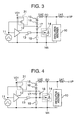
- FIG. 3 A third embodiment of the present invention is illustrated in Fig. 3.
- reference numerals 11, 12, 13 and 14 denote an on-off control signal, driver, resister and NMOS transistor, respectively.
- the output of the driver 12 is connected to the gate of the NMOS transistor 14 via the resister 13.
- Reference numerals 14 and 15 denote series-connected constant voltage diodes having their cathodes which are connected to the drain of the NMOS transistor 14.
- a diode 17 has its anode and cathode which are connected to the anode of the constant voltage diode 16 and the gate of the NMOS transistor 14, respectively.
- Bias current supply means 31 is further provided between the connecting point between the constant voltage diode 16 and the diode 17, and a power supply VD1.
- a reference Lw1 denotes the parasitic inductance of the wiring of a power source VP and Lw2 denotes the parasitic inductance which is the total inductance of the inductances of the respective terminals of the constant voltage diodes 15 and 16 and the diode 17 and the inductance of the wiring which is connected therebetween.
- a reference numeral 10 denotes a radio frequency oscillation absorbing circuit which is connected between the drain and the source of the NMOS transistor.
- the on-off control signal 11 is a signal for turning on the NMOS transistor 14
- a small current is caused to flow through the diode 17 from the bias current supply means 31 so that the diode 17 is forward-biased in advance at about 0.7 V.
- This causes a forward current to also flow through the diode 17 immediately when the current begins to flow through the constant voltage diodes 15, 16 due to occurrence of the kickback voltage. Since the forward recovery time of the diode 17 becomes substantially zero by this bias effect, the feedback path is more quickly formed for the kickback voltage, so that the peak P1 of the surge voltage shown in Fig. 18 can be advantageously lowered.
- FIG. 4 A fourth embodiment of the present invention is illustrated in Fig. 4.
- reference numerals 11, 12, 13 and 14 denote an on-off control signal, driver, resister and NMOS transistor, respectively.
- the output of the driver 12 is connected to the gate of the NMOS transistor 14 via the resister 13.
- Reference numerals 14 and 15 denote series-connected constant voltage diodes having their cathodes which are connected to the drain of the NMOS transistor 14.
- a diode 17 has its anode and cathode which are connected to the anode of the constant voltage diode 16 and the gate of the NMOS transistor 14, respectively.
- a capacitor 18 is connected in parallel with the diode 17.
- a reference Lw1 denotes a parasitic inductance of the wiring of a power source VP and Lw2 denotes a parasitic inductance which is the total inductance of the inductances of the respective terminals of the constant voltage diodes 15 and 16 and the diode 17 and the inductance of the wiring which is connected therebetween.
- a reference numeral 10 denotes a radio frequency oscillation absorbing means which is connected between the drain and the source of the NMOS transistor.
- the on-off control signal 11 is a signal for turning on the NMOS transistor 14
- a small current is caused to flow through the diode 17 from the bias current supply means 31 so that the diode 17 is forward-biased in advance at about 0.7 V.
- the present embodiment is substantially identical with that in Fig. 3 except that the capacitor 18 is connected in parallel with the diode 17.
- the feedback path is more quickly formed for the kickback voltage due to the bias effect of the diode and the cancellation effect on the inductive impedance of the feedback path by the capacitor 18, so that the peak P1 of the surge voltage shown in Fig. 18 can be advantageously lowered.
- the operation of this circuit and the effect when this circuit is used for the power converter are identical with those in Fig. 1.
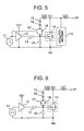
- FIG. 5 A fifth embodiment of the present invention is illustrated in Fig. 5.
- reference numerals 11, 12, 13 and 14 denote an on-off control signal, driver, resister and NMOS transistor, respectively.
- the output of the driver 12 is connected to the gate of the NMOS transistor 14 via the resister 13.
- Reference numerals 14 and 15 denote series-connected constant voltage diodes having their cathodes which are connected to the drain of the NMOS transistor 14.
- a reference numeral 57 denotes an NMOS transistor having the drain which is connected to the anode of the constant voltage diode 16, the source which is connected with the gate of the NMOS transistor 14 and the gate which is connected to the control signal 11.
- a capacitor 18 is connected in parallel with the NMOS transistor 57.
- a reference Lwl denotes the parasitic inductance of the wiring of a power source VP and Lw2 denotes the parasitic inductance which is a total inductance of the inductances of the respective terminals of the constant voltage diodes 15 and 16 and the diode 17 and the inductance of the wiring which is connected therebetween.
- a reference numeral 10 denotes a radio frequency oscillation absorbing circuit which is connected between the drain and the source of the NMOS transistor.
- NMOS 57 which is controlled in response to the on-off control signal 11 has functions which are equivalent to those of the reverse-blocking diode used in Figs. 1 to 4. Since the NMOS transistor has been turned on prior to the occurrence of the kickback voltage, the forward recovery becomes faster like the diode, so that the peak P1 of the surge voltage shown in Fig. 18 can be further lowered. The other operation of this circuit and the effect when this circuit are used for the power converter is identical with those in Fig. 1.
- FIG. 6 A sixth embodiment of the present inventing is illustrated in Fig. 6.
- reference numerals 11, 12, 13 and 14 denote an on-off control signal, driver, resister and NMOS transistor, respectively.
- the output of the driver 12 is connected to the gate of the NMOS transistor via the resister 13.
- Reference numerals 14 and 15 denote series-connected constant voltage diodes having their cathodes which are connected to the drain of the NMOS transistor 14.
- a diode 17 has its anode and cathode which are connected to the anode of the constant voltage diode 16 and the gate of the NMOS transistor 14, respectively.
- a capacitor 18 is connected in parallel with the diode 17.
- a reference Lw1 denotes the parasitic inductance of the wiring of a power source VP and Lw2 denotes a parasitic inductance which is a total inductance of the inductances of the respective terminals of the constant voltage diodes 15 and 16 and the diode 17 and the inductance of the wiring which connects them.
- the present embodiment is substantially identical with the embodiment in Fig. 1 except that the radio frequency oscillation absorbing means 10 is omitted.
- the application in which the present embodiment is effective is an application in which the embodiment is applied to a system in which the negative feedback oscillation on clamping of the surge voltage is low and that the parasitic inductance of the wiring can be made low so that a problem of the oscillation due to resonance does not substantially occur. In this case, reduction in the number of parts of the system and the mounting area in comparison to the embodiment in Fig. 1 is achieved.
- the operation of this circuit and the effect when this circuit is used for the power converter are identical to those in Fig. 1.
- FIG. 7 A seventh embodiment of the present inventing is illustrated in Fig. 7.
- reference numerals 11, 12, 13 and 14 denote an on-off control signal, driver, resister and NMOS transistor, respectively.
- the output of the driver 12 is connected to the gate of the NMOS transistor 14 via the resister 13.
- Reference numerals 14 and 15 denote series-connected constant voltage diodes having their cathodes which are connected to the drain of the NMOS transistor 14.
- a diode 17 has its anode and cathode which are connected to the anode of the constant voltage diode 16 and the gate of the NMOS transistor 14, respectively.
- a reference Lw1 denotes a parasitic inductance of the wiring of a power source VP and Lw2 denotes the parasitic inductance which is a total inductance of the inductances of the respective terminals of the constant voltage diodes 15 and 16 and the diode 17 and the inductance of the wiring which is connected therebetween.
- a reference numeral 10 denotes a radio frequency oscillation absorbing circuit which is connected between the drain and the source of the NMOS transistor 14.
- the present embodiment is substantially identical with that in Fig. 1 except that the capacitor which is connected in parallel with the reverse-blocking diode in the circuit between the drain and the gate of NMOS transistor 14 is omitted.
- the application in which the present embodiment is effective is an application in which the embodiment is applied to a system in which the negative feedback oscillation on clamping of the surge voltage is low and that the parasitic inductance of the wiring is low so that the resonance oscillation due to the parasitic induction Lw1 and the parasitic capacitance does not matter. In this case, reduction in the number of parts of the system and the mounting area in comparison to the embodiment in Fig. 1 is achieved.
- the operation of this circuit and the effect when this circuit is used for the power converter are identical to those in Fig. 1.
- FIG. 8 An eighth embodiment of the present invention is illustrated in Fig. 8.
- reference numerals 11, 12, 13 and 14 denote an on-off control signal, driver, resister and NMOS transistor having its source connected to U-phase of three-phase electric motor 82, respectively.
- the output of the driver 12 is connected to the gate of the NMOS transistor 14 via the resister 13.
- Reference numerals 14 and 15 denote series-connected constant voltage diodes having their cathodes which are connected to the drain of the NMOS transistor 14.
- a diode 17 has its anode and cathode which are connected to the anode of the constant voltage diode 16 and the gate of the NMOS transistor 14, respectively.
- a capacitor 18 is connected in parallel with the diode 17.
- a reference Lw1 denotes a parasitic inductance of the wiring of a power source VP and Lw2 denotes the parasitic inductance which is a total inductance of the inductances of the respective terminals of the constant voltage diodes 15 and 16 and the diode 17 and the inductance of the wiring which is connected therebetween.
- a reference numeral 10 denotes a radio frequency oscillation absorbing circuit which is connected between the drain and the source of the NMOS transistor.
- reference numerals 111, 112, 113 and 114 denote an on-off control signal, driver, resister and NMOS transistor having its drain connected to U-phase of three-phase electric motor 82, respectively.
- the output of the driver 112 is connected to the gate of the NMOS transistor 114 via the resister 113.
- Reference numerals 114 and 115 denote series-connected constant voltage diodes having their cathodes which are connected to the drain of the NMOS transistor 114.
- a diode 117 has its anode and cathode which are connected to the anode of the constant voltage diode 116 and the gate of the NMOS transistor 114, respectively.
- a capacitor 118 is connected in parallel with the diode 117.
- a reference Lw3 denotes a parasitic inductance which is the total inductance of the inductances of the respective terminals of the constant voltage diodes 115 and 116 and the diode 117 and the inductance of the wiring which is connected therebetween.
- a reference numeral 110 denotes a radio frequency oscillation absorbing circuit which is connected between the drain and the source of the NMOS transistor.
- the operation of above-mentioned respective circuits is identical to that in Fig. 1.
- a circuit which is identical to the above-mentioned circuit is provided for each of the other V and W phases of the three-phase electric motor 82.
- the on-off control signals 11, 111 and relevant on-off control signal for the other phases (phases V and W) are consecutively applied in a predetermined sequence to provide the three-phase electric motor 82 with an a.c. power.
- the surge voltage due to kickback can be quickly clamped in the three-phase power converter in the present embodiment, it is not necessary to provide the rated voltage of the switching elements 14, 114 with excessive margin. Accordingly, switching elements having a turn-on resistance lower than that of the prior art can be used, so that a power converter which is less in size, cost and turn-on loss can be implemented. Since the radio frequency oscillation in switched wave form can be suppressed to a sufficiently low level by means of radio frequency oscillation absorbing means in the three-phase power converter using the present embodiment, a power converter which emits less EMI noise which otherwise gives an adverse influence upon peripheral electronic circuits and equipment can be implemented.
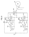
- FIG. 9 A ninth embodiment of the present invention is illustrated in Fig. 9.
- three-terminal radio frequency oscillation absorbing means 901 is provided in lieu of the radio frequency oscillation absorbing circuits 10, 110 in Fig. 8.
- This absorbing means 901 comprises series-connected capacitors Cl and C2, which are connected to the positive and negative terminals of a power source 81.
- a resister R0 is connected between the connection between the capacitors C1 and C2 and the connection between the NMOS transistors 14, 114 (U-phase in the figure).
- the radio frequency oscillation of the NMOS transistor 14 is absorbed by a path extending through the drain of the NMOS transistor 14 - capacitor C1 - resister R0 - the source of the NMOS transistor 14.
- the radio frequency oscillation of the NMOS transistor 114 is absorbed by a path extending through the drain of the MOS transistor 114 -resistor R0 - capacitor C2 - the source of the NMOS transistor 114.
- the radio frequency oscillation absorbing circuit of the present embodiment not only can absorb the radio frequency oscillation on switching of the NMOS transistors, but also serves as a bypass capacitor for the power source since the capacitor C1 and C2 are connected in series with the positive and negative terminals of the power source 81 as is apparent from the figure.
- the oscillation absorbing circuit also has an effect of reducing the noise of the power source. The other effects are identical to those in Fig. 8.
- FIG. 20 A main circuit of a three-phase inverter to which the embodiment in Fig. 8 or 9 is applied is shown in Fig. 20.
- the driver circuit and the circuit for absorbing the oscillation are omitted for clarity of illustration.
- the D.C. power of an D.C. power source 81 is converted to an A.C. power by turning on or off each of the MOSFETs which constitute a main circuit 200.
- the A.C. power is supplied to the three-phase induction electric motor 82 for driving the same.
- Each MOSFET is turned on or off by PWM control, etc.
- each MOFET is illustrated in the upper and lower arms of each phase in Fig. 20, a plurality of MOSFETs may be connected in series, in parallel or in series-parallel.
- FIG. 10 A tenth embodiment of the present invention is illustrated in Fig. 10.
- reference numerals 11, 12, 13 and 14 denote an on-off control signal, driver, resister and NMOS transistor, respectively.
- the output of the driver 12 is connected to the gate of the NMOS transistor 14 via the resister 13.
- Reference numerals 14 and 15 denote series-connected constant voltage diodes having their cathodes which are connected to the drain of the NMOS transistor 14.
- a diode 17 has its anode and cathode which are connected to the anode of the constant voltage diode 16 and the gate of the NMOS transistor 14, respectively.
- a capacitor 18 is connected in parallel with the diode 17.
- a reference Lwl denotes a parasitic inductance of the wiring of a power source VP and Lw2 denotes a parasitic inductance which is a total inductance of the inductances of the respective terminals of the constant voltage diodes 15 and 16 and the diode 17 and the inductance of the wiring which is connected therebetween.
- a reference numeral 10 denotes a radio frequency oscillation absorbing circuit which is connected between the drain and the source of the NMOS transistor.
- the present embodiment is substantially identical with the embodiment in Fig. 1 except that the driver 101 has a capability of limiting the output sink current unlike the usual drivers.
- Embodiments of the driver having a sink current limiting capability are shown in Figs. 13 and 14.
- PMOS 131 and NMOS 132 constitute a common CMOS converter.
- a resister 133 is connected between the NMOS 132 and a low voltage power source VL.
- a resister does not act as only an impedance, but gives a negative feedback action on the bias voltage between the gate and the source of the NMOS 132. In other word, stronger negative feedback takes place as higher current flows, resulting in that the resister will act to suppress the current.
- stronger negative feedback takes place as higher current flows, resulting in that the resister will act to suppress the current.
- the PMOS 141 and NMOS 142 constitute a common CMOS inverter.
- An NMOS 143 having its gate which is biased at a predetermined voltage Vb is connected between the source of the NMOS 142 and the low voltage power source VL.
- the sink current flowing through the NMOS 142 is limited to the current value of a constant current circuit including the NMOS 143.
- Use of the driver having the above-mentioned capability of limiting the above-mentioned sink current allows the current flowing through the constant voltage diodes 15,16 to be restricted to a predetermined lower value when the surge voltage clamping operation is conducted by these constant voltage diodes. Accordingly, low current parts which are inexpensive and compact can be advantageously used. The other effects are identical with those in Fig. 1.
- FIG. 11 An eleventh embodiment of the present invention is shown in Fig. 11.
- the present embodiment is substantially identical to the embodiment in Fig. 10 except that the reverse-blocking diode is replaced with a Schottky barrier diode 117.
- the effect of the Schottky barrier diode is identical with that which has been described with reference to the embodiment in Fig. 2.
- the effect of the driver 101 having a capability of restricting the sink current is identical to that which has been described in the description of the embodiment in Fig. 10.
- the other effects are identical to that in Fig. 1.
- Fig. 15 Another embodiment of the constant voltage element is shown in Fig. 15. Although zener diodes are used as the voltage constant voltage element in the embodiments in Figs. 1 to 11, a bipolar transistor and two resisters are additionally used. This allows a desired constant voltage to be finely set only by changing the ratio of the resister R1 to the resister R2.
- FIG. 19 A preferred semiconductor which is preferred for the power inverter of the present invention is shown in Fig. 19.
- reference numerals 1900, 1901, 1902, 1903, 1904 and 1905 denote a semiconductor chip, NMOS transistor, constant voltage elements, diode and gate protecting element for the NMOS transistor 1901.
- P1 to P4 denote terminals leading from the semiconductor chip to the outside thereof.
- conventional semiconductor device has at least three external terminals P1 to P3, the device has an additional fourth terminal P4 in addition to the above-mentioned external terminals.
- the fourth terminal P4 is led from a connection between the anode of the constant voltage element 1903 and the anode of the diode 1904. Addition of this terminal P4 provides an advantage that the active clamping circuit in the embodiment in Fig. 1 can be formed of only one externally added capacitor. Since the elements 1901 to 1904 are formed on the same semiconductor chip, the inductance which is parasitic to each terminal is very lower than that of conventional discrete part. Accordingly, the capacitance of the external capacitor 1 can be made lower.
- the foregoing embodiments are applicable to various voltage driven semiconductor switching elements such as semiconductor devices which have an isolated gate, for example, MOSFET as well as IGBT.
- the surge voltage due to kickback can be quickly clamped in the power converter in accordance with the present invention, it is not necessary to provide the rated voltage of the switching element with excessive margin. Accordingly, a switching element having a turn-on resistance lower than that of the prior art can be used, so that a power converter which is less in size, cost and turn-on loss can be implemented. Since the radio frequency oscillation in switched wave form can be suppressed to a sufficiently low level in the power converter using the present embodiment, a power converter which emits less EMI noise which otherwise gives an adverse influence upon peripheral electronic circuits and equipment can be implemented.
Landscapes
- Engineering & Computer Science (AREA)
- Power Engineering (AREA)
- Inverter Devices (AREA)
- Power Conversion In General (AREA)
- Control Of Voltage And Current In General (AREA)
- Electronic Switches (AREA)
Applications Claiming Priority (2)
| Application Number | Priority Date | Filing Date | Title |
|---|---|---|---|
| JP2000055954 | 2000-02-28 | ||
| JP2000055954A JP3598933B2 (ja) | 2000-02-28 | 2000-02-28 | 電力変換装置 |
Publications (3)
| Publication Number | Publication Date |
|---|---|
| EP1128539A2 true EP1128539A2 (de) | 2001-08-29 |
| EP1128539A3 EP1128539A3 (de) | 2003-07-23 |
| EP1128539B1 EP1128539B1 (de) | 2006-04-26 |
Family
ID=18576992
Family Applications (1)
| Application Number | Title | Priority Date | Filing Date |
|---|---|---|---|
| EP00118908A Expired - Lifetime EP1128539B1 (de) | 2000-02-28 | 2000-08-31 | Überspannungsgeschützter Stromwechselrichter mit einem spannungsgesteuerten Schaltkreis |
Country Status (4)
| Country | Link |
|---|---|
| US (1) | US6373731B1 (de) |
| EP (1) | EP1128539B1 (de) |
| JP (1) | JP3598933B2 (de) |
| DE (1) | DE60027538T2 (de) |
Cited By (4)
| Publication number | Priority date | Publication date | Assignee | Title |
|---|---|---|---|---|
| EP2518885A1 (de) * | 2009-12-24 | 2012-10-31 | Panasonic Corporation | Stromumrichter mit halbleiterschaltelement |
| EP3163733A1 (de) * | 2015-10-28 | 2017-05-03 | Audi Ag | Wechseleinrichter für eine elektrische maschine, elektrische antriebseinrichtung für ein kraftfahrzeug sowie verfahren zum betreiben eines wechselrichters |
| EP3244536A1 (de) * | 2016-05-11 | 2017-11-15 | Valeo Systemes de Controle Moteur | Spannungsbegrenzungsschaltkreis, schaltersystem und elektrischer leistungswandler |
| EP3467871A4 (de) * | 2016-06-02 | 2019-07-03 | Mitsubishi Electric Corporation | Stromwandler |
Families Citing this family (42)
| Publication number | Priority date | Publication date | Assignee | Title |
|---|---|---|---|---|
| JP3812353B2 (ja) * | 2001-03-19 | 2006-08-23 | 株式会社日立製作所 | 半導体電力変換装置 |
| DE10231198A1 (de) * | 2002-07-10 | 2004-01-29 | eupec Europäische Gesellschaft für Leistungshalbleiter mbH | Verfahren und Schaltungsanordnung zum Begrenzen einer Überspannung |
| JP4359250B2 (ja) | 2005-02-10 | 2009-11-04 | 株式会社日立製作所 | インターフェース回路及び電力変換装置並びに車載用電機システム |
| US20060214704A1 (en) * | 2005-03-24 | 2006-09-28 | Nec Electronics Corporation | Load drive circuit |
| EP1748539B1 (de) * | 2005-07-29 | 2018-06-06 | TDK Corporation | Schaltnetzteil mit Überspannungsunterdrückung |
| JP4343897B2 (ja) | 2005-12-12 | 2009-10-14 | 三菱電機株式会社 | 電力変換装置 |
| JP4432953B2 (ja) * | 2006-09-27 | 2010-03-17 | 株式会社日立製作所 | 半導体電力変換装置 |
| US8369109B2 (en) * | 2006-11-09 | 2013-02-05 | Osram Gesellschaft Mit Beschrankter Haftung | Self-oscillating bipolar transistor DC/AC/DC converter using a pulse forming timer |
| US20080123239A1 (en) * | 2006-11-28 | 2008-05-29 | Emerson Electric Co. | Transient voltage surge suppressor |
| JP2009011013A (ja) * | 2007-06-26 | 2009-01-15 | Hitachi Ltd | 電力変換装置 |
| JP4333802B1 (ja) | 2008-03-18 | 2009-09-16 | トヨタ自動車株式会社 | インバータの駆動装置 |
| JP5157011B2 (ja) * | 2008-04-28 | 2013-03-06 | 株式会社小松製作所 | スイッチング装置のサージ電圧抑制回路 |
| JP4992876B2 (ja) * | 2008-09-30 | 2012-08-08 | 三菱電機株式会社 | インバータ装置 |
| KR101014152B1 (ko) | 2008-10-15 | 2011-02-14 | 기아자동차주식회사 | 차량 인버터 회로 및 그를 이용한 차량 |
| JP5309923B2 (ja) * | 2008-11-21 | 2013-10-09 | 富士電機株式会社 | 半導体素子の駆動回路 |
| JP5287294B2 (ja) * | 2009-01-28 | 2013-09-11 | 富士電機株式会社 | 半導体保護回路 |
| US7990743B2 (en) * | 2009-10-20 | 2011-08-02 | General Electric Company | System and method for decreasing solar collector system losses |
| US7855906B2 (en) * | 2009-10-26 | 2010-12-21 | General Electric Company | DC bus voltage control for two stage solar converter |
| DE102009046615A1 (de) * | 2009-11-11 | 2011-05-19 | Zf Friedrichshafen Ag | Leistungsschalteranordnung für einen Wechselrichter |
| US8050062B2 (en) * | 2010-02-24 | 2011-11-01 | General Electric Company | Method and system to allow for high DC source voltage with lower DC link voltage in a two stage power converter |
| JP5682269B2 (ja) | 2010-12-06 | 2015-03-11 | サンケン電気株式会社 | ゲート駆動回路及び半導体装置 |
| US8441770B2 (en) * | 2011-02-18 | 2013-05-14 | ETA Semiconductor Inc | Voltage spikes control for power converters |
| JP5344005B2 (ja) * | 2011-06-07 | 2013-11-20 | 株式会社豊田自動織機 | スイッチング回路 |
| IN2014DN03024A (de) | 2011-12-07 | 2015-05-08 | Tm4 Inc | |
| AT512623B1 (de) * | 2012-03-06 | 2016-07-15 | Felix Dipl Ing Dr Himmelstoss | Spannungsbegrenzer mit Rückspeisung |
| CN102611288B (zh) * | 2012-03-19 | 2014-05-14 | 南京航空航天大学 | 氮化镓功率晶体管三电平驱动方法 |
| JP5796599B2 (ja) * | 2013-05-23 | 2015-10-21 | 株式会社デンソー | 半導体モジュールおよびスイッチング素子の駆動装置 |
| US8847656B1 (en) * | 2013-07-03 | 2014-09-30 | Honeywell International Inc. | Approach for driving multiple MOSFETs in parallel for high power solid state power controller applications |
| JP6129677B2 (ja) * | 2013-08-05 | 2017-05-17 | 日立オートモティブシステムズ株式会社 | 電動モータの駆動制御装置 |
| DE102013219670A1 (de) * | 2013-09-30 | 2015-04-02 | Robert Bosch Gmbh | Inverterschaltung |
| JP6156073B2 (ja) | 2013-11-08 | 2017-07-05 | 株式会社明電舎 | 半導体スイッチング素子の保護回路および電力変換装置 |
| JP6255997B2 (ja) * | 2013-12-27 | 2018-01-10 | 富士通株式会社 | 半導体装置 |
| DE112014006953T5 (de) * | 2014-09-11 | 2017-06-08 | Mitsubishi Electric Corporation | Halbleitervorrichtung |
| JP6371739B2 (ja) * | 2015-08-05 | 2018-08-08 | 日立オートモティブシステムズ株式会社 | 誘導性負荷駆動装置 |
| DE102015118165A1 (de) * | 2015-10-23 | 2017-04-27 | Infineon Technologies Ag | Elektrische baugruppe, umfassend eine halbleiterschaltvorrichtung und eine klemmdiode |
| CN107332543A (zh) * | 2016-04-28 | 2017-11-07 | 中兴通讯股份有限公司 | 一种电子接触器的保护电路及系统 |
| JP2017208988A (ja) * | 2016-05-20 | 2017-11-24 | 新電元工業株式会社 | スイッチング電源装置及びクランプ型半導体装置 |
| JP6757637B2 (ja) * | 2016-09-23 | 2020-09-23 | 株式会社ケーヒン | 誘導性負荷駆動装置 |
| DE102017219499A1 (de) * | 2017-11-02 | 2019-05-02 | Siemens Aktiengesellschaft | Elektrische Anordnung mit Teilmodulen sowie Teilmodule als solche |
| US10277107B1 (en) * | 2017-12-27 | 2019-04-30 | Stmicroelectronics S.R.L. | Synchronous rectifier gate driver with active clamp |
| WO2021028330A1 (en) * | 2019-08-12 | 2021-02-18 | Signify Holding B.V. | Mosfet circuit, for example for use in a tapped linear driver, and surge protection method |
| CN116131581B (zh) * | 2023-04-17 | 2023-07-04 | 湖南大学 | 集成振荡抑制电路的功率模块及方法 |
Citations (15)
| Publication number | Priority date | Publication date | Assignee | Title |
|---|---|---|---|---|
| JPS61244278A (ja) * | 1985-04-19 | 1986-10-30 | Matsushita Electric Works Ltd | インバ−タ装置 |
| JPS62147969A (ja) * | 1985-12-23 | 1987-07-01 | Matsushita Electric Works Ltd | インバ−タ装置 |
| JPS63114315A (ja) * | 1986-10-30 | 1988-05-19 | Nec Corp | 直流クランプ回路 |
| JPH02298067A (ja) * | 1989-05-12 | 1990-12-10 | Nec Corp | コレクタクランプ回路 |
| JPH0575439A (ja) * | 1991-09-11 | 1993-03-26 | Nec Corp | Ttl回路 |
| JPH05251970A (ja) * | 1992-03-04 | 1993-09-28 | Yokogawa Electric Corp | クランプ回路 |
| JPH06326579A (ja) * | 1993-05-12 | 1994-11-25 | Tokai Rika Co Ltd | Mos−fet を用いた負荷駆動回路 |
| JPH07213076A (ja) * | 1994-01-24 | 1995-08-11 | Mitsubishi Electric Corp | 3レベルインバータ装置 |
| EP0680147A2 (de) * | 1994-04-28 | 1995-11-02 | Mitsubishi Denki Kabushiki Kaisha | Halbleiter-Leistungsmodul und -Leistungswandlervorrichtung |
| JPH0832417A (ja) * | 1994-07-14 | 1996-02-02 | Hamamatsu Photonics Kk | 同期検出回路 |
| JPH08214545A (ja) * | 1995-01-31 | 1996-08-20 | Nippon Steel Corp | スイッチング電力変換装置 |
| JPH09139660A (ja) * | 1995-11-16 | 1997-05-27 | Mitsubishi Electric Corp | 半導体スイッチ回路 |
| JPH1155937A (ja) * | 1997-07-30 | 1999-02-26 | Denso Corp | 誘導性負荷の駆動回路 |
| EP0902537A2 (de) * | 1997-09-15 | 1999-03-17 | Siemens Aktiengesellschaft | Schaltungsanordnung zur Begrenzung von Überspannungen bei Leistungshalbleitern |
| JPH11261064A (ja) * | 1998-03-10 | 1999-09-24 | Nissan Motor Co Ltd | パワーmosfet回路 |
Family Cites Families (2)
| Publication number | Priority date | Publication date | Assignee | Title |
|---|---|---|---|---|
| JPS59201676A (ja) * | 1983-04-28 | 1984-11-15 | Canon Inc | フライバックトランスを用いた電源装置 |
| SE9500761D0 (sv) * | 1995-03-02 | 1995-03-02 | Abb Research Ltd | Skyddskrets för seriekopplade krafthalvledare |
-
2000
- 2000-02-28 JP JP2000055954A patent/JP3598933B2/ja not_active Expired - Lifetime
- 2000-08-31 EP EP00118908A patent/EP1128539B1/de not_active Expired - Lifetime
- 2000-08-31 DE DE60027538T patent/DE60027538T2/de not_active Expired - Lifetime
- 2000-09-01 US US09/654,084 patent/US6373731B1/en not_active Expired - Lifetime
Patent Citations (15)
| Publication number | Priority date | Publication date | Assignee | Title |
|---|---|---|---|---|
| JPS61244278A (ja) * | 1985-04-19 | 1986-10-30 | Matsushita Electric Works Ltd | インバ−タ装置 |
| JPS62147969A (ja) * | 1985-12-23 | 1987-07-01 | Matsushita Electric Works Ltd | インバ−タ装置 |
| JPS63114315A (ja) * | 1986-10-30 | 1988-05-19 | Nec Corp | 直流クランプ回路 |
| JPH02298067A (ja) * | 1989-05-12 | 1990-12-10 | Nec Corp | コレクタクランプ回路 |
| JPH0575439A (ja) * | 1991-09-11 | 1993-03-26 | Nec Corp | Ttl回路 |
| JPH05251970A (ja) * | 1992-03-04 | 1993-09-28 | Yokogawa Electric Corp | クランプ回路 |
| JPH06326579A (ja) * | 1993-05-12 | 1994-11-25 | Tokai Rika Co Ltd | Mos−fet を用いた負荷駆動回路 |
| JPH07213076A (ja) * | 1994-01-24 | 1995-08-11 | Mitsubishi Electric Corp | 3レベルインバータ装置 |
| EP0680147A2 (de) * | 1994-04-28 | 1995-11-02 | Mitsubishi Denki Kabushiki Kaisha | Halbleiter-Leistungsmodul und -Leistungswandlervorrichtung |
| JPH0832417A (ja) * | 1994-07-14 | 1996-02-02 | Hamamatsu Photonics Kk | 同期検出回路 |
| JPH08214545A (ja) * | 1995-01-31 | 1996-08-20 | Nippon Steel Corp | スイッチング電力変換装置 |
| JPH09139660A (ja) * | 1995-11-16 | 1997-05-27 | Mitsubishi Electric Corp | 半導体スイッチ回路 |
| JPH1155937A (ja) * | 1997-07-30 | 1999-02-26 | Denso Corp | 誘導性負荷の駆動回路 |
| EP0902537A2 (de) * | 1997-09-15 | 1999-03-17 | Siemens Aktiengesellschaft | Schaltungsanordnung zur Begrenzung von Überspannungen bei Leistungshalbleitern |
| JPH11261064A (ja) * | 1998-03-10 | 1999-09-24 | Nissan Motor Co Ltd | パワーmosfet回路 |
Non-Patent Citations (13)
| Title |
|---|
| PATENT ABSTRACTS OF JAPAN vol. 011, no. 092 (E-491), 24 March 1987 (1987-03-24) & JP 61 244278 A (MATSUSHITA ELECTRIC WORKS LTD), 30 October 1986 (1986-10-30) * |
| PATENT ABSTRACTS OF JAPAN vol. 011, no. 384 (E-565), 15 December 1987 (1987-12-15) & JP 62 147969 A (MATSUSHITA ELECTRIC WORKS LTD), 1 July 1987 (1987-07-01) * |
| PATENT ABSTRACTS OF JAPAN vol. 012, no. 357 (E-662), 26 September 1988 (1988-09-26) & JP 63 114315 A (NEC CORP), 19 May 1988 (1988-05-19) * |
| PATENT ABSTRACTS OF JAPAN vol. 015, no. 078 (E-1037), 22 February 1991 (1991-02-22) & JP 02 298067 A (NEC CORP), 10 December 1990 (1990-12-10) * |
| PATENT ABSTRACTS OF JAPAN vol. 017, no. 401 (E-1404), 27 July 1993 (1993-07-27) & JP 05 075439 A (NEC CORP), 26 March 1993 (1993-03-26) * |
| PATENT ABSTRACTS OF JAPAN vol. 018, no. 010 (E-1487), 10 January 1994 (1994-01-10) & JP 05 251970 A (YOKOGAWA ELECTRIC CORP), 28 September 1993 (1993-09-28) * |
| PATENT ABSTRACTS OF JAPAN vol. 1995, no. 02, 31 March 1995 (1995-03-31) & JP 06 326579 A (TOKAI RIKA CO LTD), 25 November 1994 (1994-11-25) * |
| PATENT ABSTRACTS OF JAPAN vol. 1995, no. 11, 26 December 1995 (1995-12-26) & JP 07 213076 A (MITSUBISHI ELECTRIC CORP), 11 August 1995 (1995-08-11) * |
| PATENT ABSTRACTS OF JAPAN vol. 1996, no. 06, 28 June 1996 (1996-06-28) & JP 08 032417 A (HAMAMATSU PHOTONICS KK), 2 February 1996 (1996-02-02) * |
| PATENT ABSTRACTS OF JAPAN vol. 1996, no. 12, 26 December 1996 (1996-12-26) & JP 08 214545 A (NIPPON STEEL CORP), 20 August 1996 (1996-08-20) * |
| PATENT ABSTRACTS OF JAPAN vol. 1997, no. 09, 30 September 1997 (1997-09-30) & JP 09 139660 A (MITSUBISHI ELECTRIC CORP), 27 May 1997 (1997-05-27) * |
| PATENT ABSTRACTS OF JAPAN vol. 1999, no. 05, 31 May 1999 (1999-05-31) & JP 11 055937 A (DENSO CORP), 26 February 1999 (1999-02-26) * |
| PATENT ABSTRACTS OF JAPAN vol. 1999, no. 14, 22 December 1999 (1999-12-22) & JP 11 261064 A (NISSAN MOTOR CO LTD), 24 September 1999 (1999-09-24) * |
Cited By (10)
| Publication number | Priority date | Publication date | Assignee | Title |
|---|---|---|---|---|
| EP2518885A1 (de) * | 2009-12-24 | 2012-10-31 | Panasonic Corporation | Stromumrichter mit halbleiterschaltelement |
| EP2518885A4 (de) * | 2009-12-24 | 2015-02-18 | Panasonic Corp | Stromumrichter mit halbleiterschaltelement |
| US9036384B2 (en) | 2009-12-24 | 2015-05-19 | Panasonic Intellectual Property Management Co., Ltd. | Power converter having semiconductor switching element |
| EP3163733A1 (de) * | 2015-10-28 | 2017-05-03 | Audi Ag | Wechseleinrichter für eine elektrische maschine, elektrische antriebseinrichtung für ein kraftfahrzeug sowie verfahren zum betreiben eines wechselrichters |
| CN106655861A (zh) * | 2015-10-28 | 2017-05-10 | 奥迪股份公司 | 用于电机的逆变器、用于机动车的电驱动装置以及用于运行逆变器的方法 |
| US9899950B2 (en) | 2015-10-28 | 2018-02-20 | Audi Ag | Inverter for an electric machine, electric drive device for a motor vehicle and method for operating an inverter |
| EP3244536A1 (de) * | 2016-05-11 | 2017-11-15 | Valeo Systemes de Controle Moteur | Spannungsbegrenzungsschaltkreis, schaltersystem und elektrischer leistungswandler |
| FR3051301A1 (fr) * | 2016-05-11 | 2017-11-17 | Valeo Systemes De Controle Moteur | Circuit de limitation de tension, systeme d'interrupteur et convertisseur electrique |
| EP3467871A4 (de) * | 2016-06-02 | 2019-07-03 | Mitsubishi Electric Corporation | Stromwandler |
| US10886247B2 (en) | 2016-06-02 | 2021-01-05 | Mitsubishi Electric Corporation | Power converter |
Also Published As
| Publication number | Publication date |
|---|---|
| JP2001245466A (ja) | 2001-09-07 |
| EP1128539A3 (de) | 2003-07-23 |
| JP3598933B2 (ja) | 2004-12-08 |
| DE60027538D1 (de) | 2006-06-01 |
| EP1128539B1 (de) | 2006-04-26 |
| US6373731B1 (en) | 2002-04-16 |
| DE60027538T2 (de) | 2006-12-07 |
Similar Documents
| Publication | Publication Date | Title |
|---|---|---|
| EP1128539B1 (de) | Überspannungsgeschützter Stromwechselrichter mit einem spannungsgesteuerten Schaltkreis | |
| US7315439B2 (en) | Method and circuit arrangement for limiting an overvoltage | |
| US6054890A (en) | Electronic switching circuit with reduction of switching transients | |
| US5119000A (en) | Low noise motor drive circuit | |
| US6407937B2 (en) | Active overvoltage protection apparatus for a bidirectional power switch in common collector mode | |
| US6094087A (en) | Gate drive circuit for isolated gate devices and method of operation thereof | |
| US5847548A (en) | Current-sharing passive snubber for parallel-connected switches and high power boost converter employing the same | |
| JP6392347B2 (ja) | スイッチング回路およびこれを備えた電源回路 | |
| US20130021067A1 (en) | Method for driving igbt | |
| US9065357B2 (en) | Power conversion circuit | |
| EP0419230A2 (de) | Dämpferschaltung eines Leistungswandlers | |
| JP5499855B2 (ja) | 電圧駆動素子の駆動回路 | |
| US7701279B2 (en) | Driving circuit for an emitter-switching configuration | |
| US5650906A (en) | Circuit arrangement for protecting power semiconductor switches which can be switched on and off against overvoltages | |
| US6438002B2 (en) | Active snubber circuit with controllable DV/DT | |
| US11539361B2 (en) | Semiconductor device signal transmission circuit for drive-control, method of controlling semiconductor device signal transmission circuit for drive-control, semiconductor device, power conversion device, and electric system for railway vehicle | |
| EP1178596B1 (de) | Wechselrichtervorrichtung | |
| US10033373B2 (en) | Half bridge having two semiconductor switches for operating a load | |
| Rodrigues et al. | Economical methods for SiC JFET’s short-circuit protection using commercial gate drivers | |
| Tang et al. | Passive resonant level shifter for suppression of crosstalk effect and reduction of body-diode loss in SiC-based bridge leg | |
| JP2009055521A (ja) | 半導体装置 | |
| EP0475704A1 (de) | Antriebsschaltkreis für einen elektrischen Motor | |
| US20230012109A1 (en) | Over-voltage protection circuitry | |
| JP2023028645A (ja) | パワー半導体モジュール、並びにそれを用いたモータ駆動システム | |
| JPH0951068A (ja) | 半導体装置 |
Legal Events
| Date | Code | Title | Description |
|---|---|---|---|
| PUAI | Public reference made under article 153(3) epc to a published international application that has entered the european phase |
Free format text: ORIGINAL CODE: 0009012 |
|
| AK | Designated contracting states |
Kind code of ref document: A2 Designated state(s): AT BE CH CY DE DK ES FI FR GB GR IE IT LI LU MC NL PT SE |
|
| AX | Request for extension of the european patent |
Free format text: AL;LT;LV;MK;RO;SI |
|
| PUAL | Search report despatched |
Free format text: ORIGINAL CODE: 0009013 |
|
| AK | Designated contracting states |
Designated state(s): AT BE CH CY DE DK ES FI FR GB GR IE IT LI LU MC NL PT SE |
|
| AX | Request for extension of the european patent |
Extension state: AL LT LV MK RO SI |
|
| RIC1 | Information provided on ipc code assigned before grant |
Ipc: 7H 02M 1/00 B Ipc: 7H 02M 7/538 A |
|
| 17P | Request for examination filed |
Effective date: 20040120 |
|
| AKX | Designation fees paid |
Designated state(s): DE FR IT |
|
| 17Q | First examination report despatched |
Effective date: 20040331 |
|
| GRAP | Despatch of communication of intention to grant a patent |
Free format text: ORIGINAL CODE: EPIDOSNIGR1 |
|
| GRAS | Grant fee paid |
Free format text: ORIGINAL CODE: EPIDOSNIGR3 |
|
| GRAA | (expected) grant |
Free format text: ORIGINAL CODE: 0009210 |
|
| AK | Designated contracting states |
Kind code of ref document: B1 Designated state(s): DE FR IT |
|
| REF | Corresponds to: |
Ref document number: 60027538 Country of ref document: DE Date of ref document: 20060601 Kind code of ref document: P |
|
| ET | Fr: translation filed | ||
| PLBE | No opposition filed within time limit |
Free format text: ORIGINAL CODE: 0009261 |
|
| STAA | Information on the status of an ep patent application or granted ep patent |
Free format text: STATUS: NO OPPOSITION FILED WITHIN TIME LIMIT |
|
| 26N | No opposition filed |
Effective date: 20070129 |
|
| PGFP | Annual fee paid to national office [announced via postgrant information from national office to epo] |
Ref country code: FR Payment date: 20130808 Year of fee payment: 14 |
|
| PGFP | Annual fee paid to national office [announced via postgrant information from national office to epo] |
Ref country code: IT Payment date: 20130819 Year of fee payment: 14 |
|
| PG25 | Lapsed in a contracting state [announced via postgrant information from national office to epo] |
Ref country code: IT Free format text: LAPSE BECAUSE OF NON-PAYMENT OF DUE FEES Effective date: 20140831 |
|
| REG | Reference to a national code |
Ref country code: FR Ref legal event code: ST Effective date: 20150430 |
|
| PG25 | Lapsed in a contracting state [announced via postgrant information from national office to epo] |
Ref country code: FR Free format text: LAPSE BECAUSE OF NON-PAYMENT OF DUE FEES Effective date: 20140901 |
|
| PGFP | Annual fee paid to national office [announced via postgrant information from national office to epo] |
Ref country code: DE Payment date: 20190820 Year of fee payment: 20 |
|
| REG | Reference to a national code |
Ref country code: DE Ref legal event code: R071 Ref document number: 60027538 Country of ref document: DE |