EP1031939B1 - Zusammengesetzte ic-karte - Google Patents
Zusammengesetzte ic-karte Download PDFInfo
- Publication number
- EP1031939B1 EP1031939B1 EP98953057A EP98953057A EP1031939B1 EP 1031939 B1 EP1031939 B1 EP 1031939B1 EP 98953057 A EP98953057 A EP 98953057A EP 98953057 A EP98953057 A EP 98953057A EP 1031939 B1 EP1031939 B1 EP 1031939B1
- Authority
- EP
- European Patent Office
- Prior art keywords
- card
- module
- coil
- antenna
- region
- Prior art date
- Legal status (The legal status is an assumption and is not a legal conclusion. Google has not performed a legal analysis and makes no representation as to the accuracy of the status listed.)
- Expired - Lifetime
Links
Images


Classifications
-
- G—PHYSICS
- G06—COMPUTING; CALCULATING OR COUNTING
- G06K—GRAPHICAL DATA READING; PRESENTATION OF DATA; RECORD CARRIERS; HANDLING RECORD CARRIERS
- G06K19/00—Record carriers for use with machines and with at least a part designed to carry digital markings
- G06K19/06—Record carriers for use with machines and with at least a part designed to carry digital markings characterised by the kind of the digital marking, e.g. shape, nature, code
-
- G—PHYSICS
- G06—COMPUTING; CALCULATING OR COUNTING
- G06K—GRAPHICAL DATA READING; PRESENTATION OF DATA; RECORD CARRIERS; HANDLING RECORD CARRIERS
- G06K7/00—Methods or arrangements for sensing record carriers, e.g. for reading patterns
- G06K7/10—Methods or arrangements for sensing record carriers, e.g. for reading patterns by electromagnetic radiation, e.g. optical sensing; by corpuscular radiation
- G06K7/10009—Methods or arrangements for sensing record carriers, e.g. for reading patterns by electromagnetic radiation, e.g. optical sensing; by corpuscular radiation sensing by radiation using wavelengths larger than 0.1 mm, e.g. radio-waves or microwaves
- G06K7/10158—Methods or arrangements for sensing record carriers, e.g. for reading patterns by electromagnetic radiation, e.g. optical sensing; by corpuscular radiation sensing by radiation using wavelengths larger than 0.1 mm, e.g. radio-waves or microwaves methods and means used by the interrogation device for reliably powering the wireless record carriers using an electromagnetic interrogation field
- G06K7/10178—Methods or arrangements for sensing record carriers, e.g. for reading patterns by electromagnetic radiation, e.g. optical sensing; by corpuscular radiation sensing by radiation using wavelengths larger than 0.1 mm, e.g. radio-waves or microwaves methods and means used by the interrogation device for reliably powering the wireless record carriers using an electromagnetic interrogation field including auxiliary means for focusing, repeating or boosting the electromagnetic interrogation field
-
- G—PHYSICS
- G06—COMPUTING; CALCULATING OR COUNTING
- G06K—GRAPHICAL DATA READING; PRESENTATION OF DATA; RECORD CARRIERS; HANDLING RECORD CARRIERS
- G06K19/00—Record carriers for use with machines and with at least a part designed to carry digital markings
- G06K19/06—Record carriers for use with machines and with at least a part designed to carry digital markings characterised by the kind of the digital marking, e.g. shape, nature, code
- G06K19/067—Record carriers with conductive marks, printed circuits or semiconductor circuit elements, e.g. credit or identity cards also with resonating or responding marks without active components
- G06K19/07—Record carriers with conductive marks, printed circuits or semiconductor circuit elements, e.g. credit or identity cards also with resonating or responding marks without active components with integrated circuit chips
- G06K19/077—Constructional details, e.g. mounting of circuits in the carrier
- G06K19/07745—Mounting details of integrated circuit chips
- G06K19/07747—Mounting details of integrated circuit chips at least one of the integrated circuit chips being mounted as a module
-
- G—PHYSICS
- G06—COMPUTING; CALCULATING OR COUNTING
- G06K—GRAPHICAL DATA READING; PRESENTATION OF DATA; RECORD CARRIERS; HANDLING RECORD CARRIERS
- G06K19/00—Record carriers for use with machines and with at least a part designed to carry digital markings
- G06K19/06—Record carriers for use with machines and with at least a part designed to carry digital markings characterised by the kind of the digital marking, e.g. shape, nature, code
- G06K19/067—Record carriers with conductive marks, printed circuits or semiconductor circuit elements, e.g. credit or identity cards also with resonating or responding marks without active components
- G06K19/07—Record carriers with conductive marks, printed circuits or semiconductor circuit elements, e.g. credit or identity cards also with resonating or responding marks without active components with integrated circuit chips
- G06K19/077—Constructional details, e.g. mounting of circuits in the carrier
- G06K19/07749—Constructional details, e.g. mounting of circuits in the carrier the record carrier being capable of non-contact communication, e.g. constructional details of the antenna of a non-contact smart card
- G06K19/0775—Constructional details, e.g. mounting of circuits in the carrier the record carrier being capable of non-contact communication, e.g. constructional details of the antenna of a non-contact smart card arrangements for connecting the integrated circuit to the antenna
- G06K19/07756—Constructional details, e.g. mounting of circuits in the carrier the record carrier being capable of non-contact communication, e.g. constructional details of the antenna of a non-contact smart card arrangements for connecting the integrated circuit to the antenna the connection being non-galvanic, e.g. capacitive
-
- G—PHYSICS
- G06—COMPUTING; CALCULATING OR COUNTING
- G06K—GRAPHICAL DATA READING; PRESENTATION OF DATA; RECORD CARRIERS; HANDLING RECORD CARRIERS
- G06K19/00—Record carriers for use with machines and with at least a part designed to carry digital markings
- G06K19/06—Record carriers for use with machines and with at least a part designed to carry digital markings characterised by the kind of the digital marking, e.g. shape, nature, code
- G06K19/067—Record carriers with conductive marks, printed circuits or semiconductor circuit elements, e.g. credit or identity cards also with resonating or responding marks without active components
- G06K19/07—Record carriers with conductive marks, printed circuits or semiconductor circuit elements, e.g. credit or identity cards also with resonating or responding marks without active components with integrated circuit chips
- G06K19/077—Constructional details, e.g. mounting of circuits in the carrier
- G06K19/07749—Constructional details, e.g. mounting of circuits in the carrier the record carrier being capable of non-contact communication, e.g. constructional details of the antenna of a non-contact smart card
- G06K19/07766—Constructional details, e.g. mounting of circuits in the carrier the record carrier being capable of non-contact communication, e.g. constructional details of the antenna of a non-contact smart card comprising at least a second communication arrangement in addition to a first non-contact communication arrangement
- G06K19/07769—Constructional details, e.g. mounting of circuits in the carrier the record carrier being capable of non-contact communication, e.g. constructional details of the antenna of a non-contact smart card comprising at least a second communication arrangement in addition to a first non-contact communication arrangement the further communication means being a galvanic interface, e.g. hybrid or mixed smart cards having a contact and a non-contact interface
-
- G—PHYSICS
- G06—COMPUTING; CALCULATING OR COUNTING
- G06K—GRAPHICAL DATA READING; PRESENTATION OF DATA; RECORD CARRIERS; HANDLING RECORD CARRIERS
- G06K19/00—Record carriers for use with machines and with at least a part designed to carry digital markings
- G06K19/06—Record carriers for use with machines and with at least a part designed to carry digital markings characterised by the kind of the digital marking, e.g. shape, nature, code
- G06K19/067—Record carriers with conductive marks, printed circuits or semiconductor circuit elements, e.g. credit or identity cards also with resonating or responding marks without active components
- G06K19/07—Record carriers with conductive marks, printed circuits or semiconductor circuit elements, e.g. credit or identity cards also with resonating or responding marks without active components with integrated circuit chips
- G06K19/077—Constructional details, e.g. mounting of circuits in the carrier
- G06K19/07749—Constructional details, e.g. mounting of circuits in the carrier the record carrier being capable of non-contact communication, e.g. constructional details of the antenna of a non-contact smart card
- G06K19/07773—Antenna details
- G06K19/07775—Antenna details the antenna being on-chip
-
- G—PHYSICS
- G06—COMPUTING; CALCULATING OR COUNTING
- G06K—GRAPHICAL DATA READING; PRESENTATION OF DATA; RECORD CARRIERS; HANDLING RECORD CARRIERS
- G06K19/00—Record carriers for use with machines and with at least a part designed to carry digital markings
- G06K19/06—Record carriers for use with machines and with at least a part designed to carry digital markings characterised by the kind of the digital marking, e.g. shape, nature, code
- G06K19/067—Record carriers with conductive marks, printed circuits or semiconductor circuit elements, e.g. credit or identity cards also with resonating or responding marks without active components
- G06K19/07—Record carriers with conductive marks, printed circuits or semiconductor circuit elements, e.g. credit or identity cards also with resonating or responding marks without active components with integrated circuit chips
- G06K19/077—Constructional details, e.g. mounting of circuits in the carrier
- G06K19/07749—Constructional details, e.g. mounting of circuits in the carrier the record carrier being capable of non-contact communication, e.g. constructional details of the antenna of a non-contact smart card
- G06K19/07773—Antenna details
- G06K19/07777—Antenna details the antenna being of the inductive type
- G06K19/07779—Antenna details the antenna being of the inductive type the inductive antenna being a coil
- G06K19/07783—Antenna details the antenna being of the inductive type the inductive antenna being a coil the coil being planar
-
- G—PHYSICS
- G06—COMPUTING; CALCULATING OR COUNTING
- G06K—GRAPHICAL DATA READING; PRESENTATION OF DATA; RECORD CARRIERS; HANDLING RECORD CARRIERS
- G06K19/00—Record carriers for use with machines and with at least a part designed to carry digital markings
- G06K19/06—Record carriers for use with machines and with at least a part designed to carry digital markings characterised by the kind of the digital marking, e.g. shape, nature, code
- G06K19/067—Record carriers with conductive marks, printed circuits or semiconductor circuit elements, e.g. credit or identity cards also with resonating or responding marks without active components
- G06K19/07—Record carriers with conductive marks, printed circuits or semiconductor circuit elements, e.g. credit or identity cards also with resonating or responding marks without active components with integrated circuit chips
- G06K19/077—Constructional details, e.g. mounting of circuits in the carrier
- G06K19/07749—Constructional details, e.g. mounting of circuits in the carrier the record carrier being capable of non-contact communication, e.g. constructional details of the antenna of a non-contact smart card
- G06K19/07773—Antenna details
- G06K19/07777—Antenna details the antenna being of the inductive type
- G06K19/07784—Antenna details the antenna being of the inductive type the inductive antenna consisting of a plurality of coils stacked on top of one another
Definitions
- the present invention relates to a smart card having both a function of a contact type in which reception of supply power, transmission/reception of signals, etc. are performed via an electrical contact, and a function of a non-contact type in which reception of supply power, transmission/reception of signals, etc. are performed without provision of an electrical contact, in an information recording medium represented by IC cards, etc. used in fields such as office automation (OA), factory automation (FA) or security.
- OA office automation
- FA factory automation
- IC cards are internationally standardized by the ISO (International Organization for Standardization).
- an IC such as a semiconductor memory is built in a card body formed of a plastic material as a basic material and metallic conductive terminal electrodes are provided on a card surface for connection with an external read/write apparatus.
- the IC card is inserted in a card slot of the external read/write apparatus and the terminal electrodes of the IC card are connected to the external read/write apparatus.
- This is suitable for uses requiring security and safety for communication as in large-volume data exchange and banking processing, for example, uses for crediting and electronic wallets.
- Radio Frequency Identification RFID
- a hard logic which does not have a battery cell and a CPU (Central Processing Unit).
- RFID Radio Frequency Identification
- CPU Central Processing Unit
- a metallic foil antenna coil for non-contact transmission which is formed by etching, is sandwiched between a sheet with engagement hole for an IC module and a substrate.
- the structure is laminated to produce a card body.
- two antenna terminals for connection between the antenna coil and the IC module are exposed to an inside of the engagement hole in the card body.
- This mounting method is relatively simple. However, it is difficult to confirm the state of the connection portion between the IC module and antenna, and a problem remains with the reliability of connection. In addition, degradation in the connection portion may easily occur due to mechanical stress. Moreover, since a step for applying the conductive adhesive and a thermocompression step are required for the connection between the IC module and antenna, it is difficult to use an apparatus for manufacturing a conventional IC card with external terminals. It is thus necessary to provide a new manufacturing line.
- an emboss or a magnetic stripe cannot be applied due to restrictions of the coil shape, etc. for keeping reception power.
- the emboss and magnetic stripe have to be considered. Techniques which do not permit provision of an emboss or a magnetic stripe are restricted in the range of application.
- a non-contact-type IC card disclosed, for example, in Jpn. Pat. Appln. KOKAI Publication No. 8-227,447 permits provision of an emboss and a magnetic stripe.
- a non-contact-type IC card having an outer shape according to ISO 7811 is provided.
- a communication IC module is constructed such that an IC mount portion, a power receiving coil and a data transmission/reception coil are arranged in a longitudinal direction on a region excluding the magnetic stripe region and embossing region.
- the reception coil and communication coil of the communication IC module are comprised of single-layer coils formed by electrocasting. Both are buried in a single strip-like substrate. Lead portions for connection with pads of the IC chip are formed of each coil.
- the IC chip is mounted on the strip-like substrate such that a circuit surface of the IC chip is opposed to the strip-like substrate.
- the lead portions are bump-bonded to the IC pads and a gap between the strip-like substrate and IC chip is filled with a potting resin for fixation.
- An inner end portion of the coil and an end portion of an internal-end lead are jumper-bonded by an enamel copper wire. The bonding is effected by instantaneous thermocompression and terminal portions are protected with potting resin.
- a method of integrating this communication IC module and the card is described. According to this method, there are provided a first sheet for covering the upper surface, a second sheet having the same thickness as the strip-like substrate and having a window with a strip-like outer shape, a third sheet having a window for passing the IC chip and a window for passing a first jumper-bonding portion, a fourth sheet having only a window for passing the IC chip, and a fifth sheet for covering the lower surface (all formed of vinyl chloride).
- the communication module is sandwiched by the respective sheets and subjected to thermocompression. Thus, the communication module is integrated in the card.
- FIG. 1 shows a magnetic stripe region, an embossing region and an external terminal region specified by ISO 7816.
- an IC module is mounted on the external terminal region.
- FIG. 1 in the regions indicated by hatching, mounting of an antenna for non-contact coupling is prohibited.
- ISO 7816 specifies an outer long side to be 85.47-85.72 mm, an outer short side to be 53.29-54.03 mm.
- the magnetic stripe region is defined in an area of 15.82 mm from the upper side.
- the embossing region is defined in an area of 24 mm from the lower side, 6.0 mm from the left side, and 8.0 mm from the right side.
- the external terminals are formed in an area of 28.55 mm from the upper side and 19.87 mm from the left side.
- Jpn. Pat. Appln. KOKAI Publication No. 7-239,922 discloses a prior-art technique of a smart card realizing a magnetic stripe and embossing.
- the IC module for the IC card comprises an IC chip; a transmission mechanism connected to the IC chip for effecting transmission of information and/or power with the external apparatus; and a support member for supporting the IC chip and transmission mechanism.
- the transmission mechanism comprises a non-contact-type transmission mechanism having a coil or an antenna, and a contact-type transmission mechanism having a plurality of terminal electrodes of patterned conductors provided on a surface of the support member.
- the document further discloses, as mounting means, that the antenna or coil for non-contact transmission is provided so as to surround the terminal electrodes, and alternatively the antenna is positioned at the center and the terminal electrodes are provided around the antenna.
- the non-contact transmission antenna is contained in the IC module and thereby the connection between the antenna coil and the IC module is omitted in the final step.
- the antenna or coil Since the distance between the terminal electrodes and embossing region is 1.45 mm at maximum, it is not practical to dispose the antenna or coil so as to surround the terminal electrodes without overlapping the terminal electrodes, as will be described below. In the case where the antenna coil is disposed around the external terminals, the maximum outside diameter and minimum inside diameter of the coil are ⁇ 12 mm and ⁇ 9.3 mm, respectively. If the antenna coil is formed of a print pattern in this region, where the pattern width and interval are 0.15 mm and 0.1 mm respectively, the number of turns and the inductance become about four and 0.4 ⁇ H, and six and 1.0 ⁇ H in respective cases ( ⁇ H denotes microhenry).
- the merit of adding the non-contact transmission function is small.
- the merit of adding the non-contact transmission mechanism to the contact type transmission mechanism is obtained with a communication distance exceeding several-ten mm to 100 mm. Communication is achieved if the card is exposed to the antenna unit of the external read/write apparatus within such an area. For this purpose, it is necessary to increase the area of the coil or the number of turns.
- the coil is disposed around the outer periphery of the terminal electrodes within the IC module, only several turns are obtained even if the print coil is formed, and owing to the smallness of the area of the coil, too, adequate power cannot be obtained. Moreover, if a practical number of turns is to be obtained with a conductor pattern, it overlaps the embossing region.
- FIG. 2 shows an equivalent circuit of a non-contact coupler circuit for describing the principle of the non-contact transmission mechanism.
- a transmission/reception circuit 101 of a non-contact type external read/write apparatus 100 is connected to a transmission/reception coil 102 which is an electromagnetic coupler for supplying power to, and exchanging information with, the non-contact transmission mechanism in the smart card.
- the non-contact transmission mechanism of the smart card 1 comprises an antenna coil 4, connected electromagnetically and directly to the transmission/reception antenna 102 of the external read/write apparatus 100, for receiving power and exchanging information; a capacitive element 15 connected between both ends of the antenna coil 4 to constitute a parallel resonance circuit; an IC chip 6 mounted on an IC module 2; a first coupler coil 8 connected to the IC chip 6; and a second coupler coil 3 closely coupled and disposed to transmit a signal received by the antenna coil 4 to the first coupler coil 8 with a maximum efficiency and connected between both ends of the capacitive element 15 of the parallel resonance circuit.
- the capacitive element 15 is connected in parallel to the antenna coil 4, it may preferably be connected in series between the antenna coil 4 and second coupler coil 3. If the parasitic capacity is increased, the capacitive element 15 can be dispensed with.
- a current is caused to flow in the parallel resonance circuit, which comprises the antenna coil 4 and capacitive element 15 of the smart card 1, due to the high-frequency magnetic field produced by the transmission/reception coil 102 of the external read/write apparatus 100.
- currents due to the high-frequency magnetic field are also induced in the first coupler coil 8 connected directly to the IC chip 6 and the second coupler coil 3 connected to the resonance circuit of the antenna coil 4 and capacitive element 15 to transmit power to the first coupler coil 8.
- the amount of induced currents in this case is less than that of current induced in the antenna coil 4 by an order of magnitude, and accordingly the sensitivity of reception depends greatly on characteristics of the antenna coil 4.
- a signal received by the resonance circuit of the antenna coil 4 and capacitive element 15 is transmitted to the second coupler coil 3. Since the second coupler coil 3 and first coupler coil 8 are closely coupled and disposed with a maximum transmission efficiency, the signal is then transmitted to the IC chip 6 via transformer coupling of the second coupler coil 3 and first coupler coil 8. The maximum transmission efficiency of transformer coupling between the second coupler coil 3 and first coupler coil 8 is determined by selection of the circuit constant.
- the antenna characteristics vary depending on the method of the non-contact transmission mechanism, such as electromagnetic coupling, electromagnetic induction, etc..
- the antenna coil characteristics with the electromagnetic induction method in a short-wave band are calculated, for example, as shown in TABLE 1.
- the thickness and pitch of the coil are 0.05 mm in the case of *1 alone. In the other cases, the thickness and pitch of the coil are 0.15 mm.
- the inductance of the antenna coil of the currently used RF-ID card for the short-wave band is about 5 microhenries.
- This type of antenna coil can be disposed on an outer peripheral portion of the card by means of a print pattern (print coil).
- Coils having more than eight turns can be realized by a spiral coil of a three-dimensional shape and a planer print coil.
- the spiral coil it is wound in an overlapping manner and thus can be disposed at an outer peripheral portion of the card.
- the print coil it is generally formed in a non-overlapping manner. Accordingly, where the number of turns is large, it is not proper to dispose the coil at the outer peripheral portion of the card so as to avoid overlapping with the embossing region.
- the card can be fabricated at low cost with simple manufacturing process and with high reliability.
- FIG. 3A and FIG. 3B show a schematic structure of a smart card according to a first arrangement.
- FIG. 3A shows the whole structure and
- FIG. 3B shows a cross-sectional structure of the mounting portion of the IC module.
- the smart card 1 according to the present arrangement is fabricated in a manner described below.
- the antenna substrate 5 is sealed by injection molding to form the card substrate 10.
- the second coupler coil 3 is positioned to overlap the mounting position of the IC module 2.
- an engagement hole 11 for the IC module 2 is formed.
- the card substrate is formed of vinyl chloride, but other materials such as polycarbonate are applicable to the present invention if characteristics of the card such as adequate strength and embossing processability are obtained.
- the card substrate 10 is shown as being divided into an obverse side portion and a reverse side portion. However, the card substrate 10 is actually a single piece. In the figure, the card substrate is shown in a modified fashion in order to clearly describe a relationship between the coupler coil and engagement hole 11 of the antenna substrate 5 which is sealed in the card substrate.
- the card is fabricated by injection molding. Any method, however, is applicable if characteristics of embossing are maintained. For instance, a laminating method or an adhesive filling method may be adopted.
- the engagement hole 11 for the IC module is made by cutting after the fabrication of the card.
- FIG. 4 is a plan view of the first arrangement of the smart card having an embossing region, showing a position of mounting of the antenna coil 4 within the smart card 1.
- the antenna coil 4 is disposed over the entire peripheral portion of the card.
- the embossing region 20 and external terminal region 21 are disposed within the loop of the antenna coil 4.
- the specifications of this coil correspond to example 1 in TABLE 1.
- FIG. 4 is effective where the number of turns of antenna coil 4 is relatively small, specifically, 3 to 7, and preferably 4 or 5.
- the antenna substrate 5 in this example of mounting that portion of the resin sheet, which corresponds to the embossing region 20, is cut out. This aims at preventing an adverse effect on embossing characteristics.
- FIGS. 4 to 7 the outer contours of the antenna substrates 5 are indicated by broken lines.
- FIG. 5 is a plan view of another smart card 1 according to a first embodiment of the invention having the embossing region.
- This figure shows a general shape of the antenna coil 4, on the outside of which the embossing region 20 and external terminal region 21 are disposed (i.e. not within the antenna coil).
- the specifications of this coil correspond to example 3 in TABLE 1.
- the example of FIG. 5 is effective where the number of turns of the antenna coil 4 is 10 or more.
- FIG. 6 is a plan view of a third example of mounting of the smart card 1 according to the first arrangement, which has both the magnetic stripe and embossing region.
- This figure shows a position of mounting of the antenna coil 4 in the smart card 1.
- the antenna coil 4 is made not to overlap the magnetic stripe region 22. That portion of the antenna coil, which excludes a portion thereof opposed to the magnetic stripe region, is disposed along the outer periphery of the smart card 1.
- the specifications of this coil correspond to example 2 in TABLE 1.
- the antenna substrate 5 in this example of mounting too, that portion of the resin sheet, which corresponds to the embossing region 20, is cut out. This aims at preventing an adverse effect on embossing characteristics.
- FIG. 7 is a plan view of a fourth example of mounting of the smart card 1 according to the first embodiment of the invention, which has both the magnetic stripe and embossing region.
- This figure shows a general shape of the antenna coil 4 which is disposed not to include the embossing region 20 or magnetic stripe region 22.
- the specifications of this coil correspond to example 4 in TABLE 1.
- the smart card according to the first arrangement has functions compatible with both the contact-type system with external terminals and the non-contact-type system with non-contact coupling elements such as an antenna coil.
- non-contact coupling elements such as an antenna coil.
- the area of the antenna coil is increased to a maximum permissible level.
- the reception sensitivity of the card is enhanced, the communication distance is increased and/or the transmission output of the external read/write apparatus can be reduced. This is convenient for cards since the transmission output is restricted by the Wireless Conducty Act.
- the antenna coil which is directly brought into non-contact coupling with the external read/write apparatus is so disposed as not to overlap the external terminal region of the non-contact-type electrodes, which is also the IC module engagement region, the embossing region and/or the magnetic stripe region, this invention permits general-purpose applications and is fully applicable to conventional cards.
- the thickness of the card can be set to fully meet the standard of ISO 7816, i.e. 0.76 mm.
- the increase in the number of turns of the first coupler coil 8 increases a coefficient of coupling with the second coupler coil 3, and energy to be transmitted to the IC chip 6 further increases.
- the limit pattern width is 0.1 mm. It is difficult to form several-ten turns of a print coil in the module substrate of the IC card.
- a coil is formed of an insulation-coated conductor wire, a diameter of several-ten microns is attained by virtue of development in magnetic head technology.
- the coupler coils for the IC module and antenna may be formed of an insulation-coated conductor wire.
- a smart card wherein no connection is required between the IC module and non-contact transmission antenna coil, a reception sensitivity capable of obtaining an adequate communication distance is attained, the IC card is compatible with both embossing processing and magnetic stripe formation, and both a contact-type and a non-contact-type transmission mechanisms are maintained in practical operation states.
- An equivalent circuit of a non-contact coupling circuit according to a second embodiment is the same as that according to the first arrangement, as shown in FIG. 2.
- FIGS. 8A and 8B show schematic structures of the smart card according to the second embodiment of the present invention.
- FIG. 8A shows the whole structure and
- FIG. 8B shows a cross-sectional structure of the mounting portion of the IC module.
- the smart card 1 comprises the IC module 2 of the present invention, and the card substrate 10 wherein the antenna substrate 5 having the second coupler coil 3 and the antenna coil 4 formed of print coils on a resin sheet surface is resin-sealed.
- the IC module 2 comprises the patterned terminal electrodes 7 serving as a contact-type transmission section; the IC chip 6 incorporating a contact-type interface and a non-contact-type interface (not shown); the first coupler coil 8 of a non-contact-type transmission section which is formed of an insulation-coated conductor wire around the IC chip 6 or module substrate 9; and the module substrate 9.
- the IC chip 6 is mounted on a surface of the module substrate 9, which is opposite to a surface thereof provided with the terminal electrodes 7.
- the IC chip 6 and the terminal electrodes 7 on the module substrate 9 are connected via through-holes.
- the IC chip 6 and a circuit pattern on the module substrate 9 for connecting the terminal electrodes 7 and first coupler coil 8 are bonded by means of thermal fusion using solder or conductive adhesive. This bonding is also realized by wire-bonding the circuit formation surface of the IC chip 6 and the module substrate 9.
- the IC chip 6 is mounted on the module substrate 9, and circuit connection is carried out. Then, the IC chip 6 is sealed with a seal resin 16, as shown in FIG. 8A. Following this, an insulation-coated conductor wire is wounded around the periphery of the IC chip 6 or the periphery of the module substrate 9, thereby forming the first coupler coil 8. Subsequently, the circuit pattern on the module substrate 9 and the terminals of the first coupler coil 8 are connected and the IC module 2 is completely fabricated.
- FIG. 8B shows a case where the first coupler coil 8 is wound around the seal resin 16 of the IC chip 6.
- the periphery of the seal resin 16 of the IC module 2 which has been formed up to the step of formation of the seal resin 16, is processed by cutting means, etc. so as to facilitate winding of a coil.
- a coil is directly wound around the resin seal 16 of the IC module by using a winding device (not shown).
- connection terminals of the first coupler coil 8 are removed and the connection terminals are connected to a predetermined circuit pattern (not shown) on the module substrate 9.
- the step of cutting the seal resin 16 can be omitted by forming the seal resin 16 with use of a mold, etc. which facilitates the winding of the coil.
- This embodiment also includes a technique wherein a coil is not directly wound around the periphery of the IC chip 6 and, instead, a planar coil is formed in a different step using a coil winding machine and is attached to the module substrate 9 to produce the first coupler coil 8, following which the seal resin 16 is provided to cover the IC chip 6 and first coupler coil 8.
- the cross-sectional shape of the formed coil is rectangular with rounded corners, but it may be circular.
- the cross-sectional shape is not limited.
- the smart card 1 is fabricated in the following manner.
- the antenna substrate 5 is prepared, wherein the second coupler coil 3, antenna coil 4 and capacitive element 15 are formed of print coils on different regions on the resin substrate.
- the second coupler coil 3 on the antenna substrate 5 is formed outside the engagement hole 11 for the IC module 2.
- the second coupler coil 3 is finally nested in substantially the same plane as the first coil 8 mounted in the IC module 2.
- the second coupler coil 3 and antenna coil 4 may be formed of insulation-coated wire.
- Vinyl chloride is used as the resin material of the antenna substrate 5.
- polycarbonate, PET, or polyimide may be applied.
- the material is not limited to one kind.
- the thickness of the antenna substrate 5 is in a range of 50 ⁇ m to 300 ⁇ m, and preferably about 100 ⁇ m.
- the card substrate 10 is formed.
- the second coupler coil 3 is positioned to overlap the position of mounting of the IC module 2.
- the engagement hole 11 for the IC module 2 is formed.
- the IC module 2 is bonded in the engagement hole 11 for IC module 2 in the card substrate 10 and the fabrication of the smart card 1 is completed.
- vinyl chloride is used as the material of the card substrate 10
- any material such as polycarbonate may be applicable to the present invention if adequate characteristics of the card are obtained.
- the card substrate 10 is shown as being divided into an obverse side portion and a reverse side portion. However, the card substrate 10 is actually a single piece.
- the card substrate is shown in a modified fashion in order to clearly describe a relationship between the coupler coil and engagement hole 11 of the antenna substrate 5 which is sealed in the card substrate.
- the card is fabricated by injection molding. Any method, however, is applicable to the present invention if characteristics of the card are maintained. For instance, a laminating method or an adhesive filling method may be adopted.
- This embodiment includes a technique wherein the engagement hole 11 for the IC module is formed at the same time as the card is formed. In this case, the inside of the second coupler coil 3 on the antenna coil 5 is cut out in advance for engagement with the IC module.
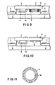
- FIG. 9 shows an example of mounting, in which the first coupler coil 8 is wound near the IC chip 6.
- the IC chip 6 is eccentrically mounted on the module substrate 9.
- the first coupler coil 8 formed separately by using a winding machine (not shown) is attached to the module substrate 9 of the IC module 2 which has been fabricated up to the step of forming the seal resin 16.
- Connection terminals (not shown) of the first coupler coil 8 are connected to a predetermined circuit pattern (not shown) on the module substrate 9.
- the IC module 2 is completely fabricated.
- the step of processing the periphery of the resin seal portion to mount the first coil 8 is not required.
- the cross-sectional shape of the formed coil is rectangular with rounded corners, it may be circular or oval. The cross-sectional shape is not limited.
- FIG. 10 shows an example of mounting, in which the first coupler coil 8 is formed of a conductor print pattern on that surface of the module substrate 9, on which the IC chip 6 is mounted, such that the first coupler coil 8 is disposed near the IC chip 6.
- the connection between the module substrate 9 and first coil 8 is made simpler.
- the cross-sectional shape of the first coupler coil 8 in this embodiment is rectangular with rounded corners, it may be circular or oval.
- the cross-sectional shape is not limited. For example, as is shown in FIG. 11, if the first coupler coil 8 with a toroidal shape is wound around the periphery of the seal resin 16 of the IC chip, the directivity to the induction electromagnetic field is increased and the degree of coupling is enhanced.
- the IC module according to the second embodiment has functions compatible with both the contact-type system with external terminals and the non-contact-type system with non-contact coupling elements such as an antenna coil.
- non-contact coupling elements such as an antenna coil.
- the inside diameter of the second coupler coil of the non-contact-transmission antenna element is made greater than the outside diameter of the engagement hole for the IC module, the first coupler coil disposed on the IC module is formed on the back surface of the module substrate, and the first and second coupler coils are disposed in substantially the same plane. Thereby, the gap is reduced and a higher coupling coefficient is obtained.
- the reception sensitivity of the card is enhanced, the communication distance is increased and/or the transmission output of the external read/write apparatus can be reduced. This is convenient for the non-contact transmission function because the transmission output is restricted by the Wireless Conducty Act.
- the inside of the second coupler coil of the non-contact-transmission antenna element serves as the engagement hole for the IC module.
- the second coupler coil is disposed below the engagement hole for the IC module, there is no need to consider depth precision in forming the engagement hole.
- Conventional equipment for forming an engagement hole in an IC card with external terminals can be applied as it is.
- no connection is required between the IC module and the antenna circuit built in the card substrate. Even if a mechanical stress such as a bending stress acts on the card, there is little possibility of fault due to breakage of connection terminals, because of the absence of any contact point between the IC module and the antenna circuit.
- the second coupler coil of the non-contact-transmission antenna element is disposed outside the antenna loop, projection of the antenna coil to the embossing region is prevented.
- An equivalent circuit of a non-contact coupling circuit according to an unclaimed embodiment is the same as that according to the first arrangement, as shown in FIG. 2.
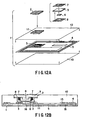
- FIGS. 12A and 12B show schematic structures of the smart card according to the embodiment.
- FIG. 12A shows the whole structure and
- FIG. 12B shows a cross-sectional structure of the mounting portion of the IC module.
- the smart card 1 according to this unclaimed embodiment comprises the IC module 2 and the card substrate 10 wherein the antenna substrate 5 having the second coupler coil 3 and the antenna coil 4 formed of print coils on a resin sheet surface is resin-sealed.
- the IC module 2 comprises the patterned terminal electrodes 7 serving as a contact-type transmission section; the IC chip 6 incorporating a contact-type interface and a non-contact-type interface (not shown); the first coupler coil 8 of a non-contact-type transmission section which is formed of an insulation-coated conductor wire around the IC chip 6 or module substrate 9; and the module substrate 9.
- This bonding is also realized by wire-bonding the circuit formation surface of the IC chip 6 and the module substrate 9.
- the IC chip 6 is mounted on the module substrate 9, and circuit connection is carried out. Then, the IC chip 6 is sealed with the seal resin 16. Following this, an insulation-coated conductor wire is wounded around the periphery of the IC chip 6 or the periphery of the module substrate 9, and the circuit pattern on the module substrate 9 and the terminals of the first coupler coil 8 are connected and the IC module 2 is completely fabricated.
- FIG. 12B shows a case where the first coupler coil 8 is wound around the seal resin 16 of the IC chip 6.
- the smart card 1 according to this unclaimed embodiment is fabricated in the following manner.
- the flexible antenna substrate 5 is prepared, wherein the second coupler coil 3, antenna coil 4 and capacitive element 15 are formed of print coils on the resin substrate.
- the second coupler coil 3 and antenna coil 4 may be formed of insulation-coated wire.
- Vinyl chloride is used as the resin material of the antenna substrate 5.
- polyimide, polycarbonate, or PET may be applied. The material is not limited to one kind.
- the card substrate 10 is formed.
- the second coupler coil 3 is positioned to overlap the position of mounting of the IC module 2.
- the engagement hole 11 for the IC module 2 is formed simultaneously with the formation of the card substrate 10 by the injection molding.
- the IC module 2 is bonded in the engagement hole 11 for IC module 2 in the card substrate 10 and the fabrication of the smart card 1 is completed.
- vinyl chloride is used as the material of the card substrate 10, any material such as polycarbonate may be applicable to the present invention if adequate characteristics of the card are obtained.
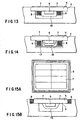
- FIG. 13 shows an example of mounting, wherein the first coupler coil 8 is wound around the IC chip 6.
- the periphery of the seal resin 16 of the IC module 2, which has been formed up to the step of formation of the seal resin 16, is processed by cutting means, etc. so as to facilitate winding of a coil.
- a coil is directly wound around the resin seal 16 of the IC module by using a winding device (not shown).
- the insulation coating (not shown) of the connection terminals of the first coupler coil 8 are removed and the connection terminals are connected to a predetermined circuit pattern (not shown) on the module substrate 9.
- the step of cutting the seal resin 16 can be omitted by forming the seal resin 16 with use of a mold, etc. which facilitates the winding of the coil.
- the coil may not be directly wound around the periphery of the IC chip 6, and a planar coil may be formed in a different step using a coil winding machine and attached to the module substrate 9 to produce the first coupler coil 8.
- the cross-sectional shape of the formed coil is rectangular with rounded corners, but it may be circular or oval.
- the cross-sectional shape is not limited.
- the first coupler coil 8 with a toroidal shape may be wound around the periphery of the seal resin 16 of the IC chip.
- FIG. 14 shows an example of mounting, wherein the first coupler coil 8 wound around a coil frame 17, which is provided around the seal resin 16 of IC chip 6, is mounted.
- the coil frame 17 is provided with terminals for connection with the coil and thereby the connection between the module substrate 9 and first coil 8 is made simpler.
- the cross-sectional shape of the coil frame 17 in this unclaimed embodiment is rectangular with rounded corners, it may be circular, etc., as with the above-described cases.
- FIGS. 15A and 15B show an example of mounting, wherein the first coupler coil 8 is wound around end faces of the module substrate 9.
- the first coupler coil 8 can also be formed by applying a coil to the periphery (in thickness direction) of the module substrate 9 of the IC module 2 with rounded corners.
- the winding of the coil around the periphery of the module substrate 9 was carried out prior to the mounting of the IC chip 6. This step may be carried out after the fabrication of the IC module 2, and the order of steps is not limited.
- the smart card according to the unclaimed embodiment has functions compatible with both the contact-type system with external terminals and the non-contact-type system with non-contact coupling elements such as an antenna coil.
- the smart card incorporating the IC module since transformer-coupling circuit elements are disposed between the IC module and antenna coil, power reception and signal transmission/reception can be effected between the IC module and antenna coil without electrical connection.
- the transformer coupling element of the IC module is realized by a coil and the coil is directly wound around the periphery of the seal resin of the IC chip.
- the planar coil prepared in advance is directly bonded to the module substrate.
- a coil is wound around the coil frame and the coil frame is bonded to the module substrate, or the coil is wound around the end faces of the module substrate.
- the number of turns of the coupler coil of the module substrate is increased as much as possible.
- electromagnetic energy received by the antenna coil can be transmitted to the IC chip by transformer coupling with a high coupling coefficient.
- the reception sensitivity of the card is enhanced, the communication distance is increased and/or the transmission output of the external read/write apparatus can be reduced. This is convenient for IC cards since the transmission output for non-contact type IC cards (smart cards) is restricted by the Wireless Conducty Act.
- a smart card and an IC module wherein, despite no connection being required between the IC module and non-contact transmission antenna coil, a reception sensitivity capable of obtaining an adequate communication distance is attained and both a contact-type and a non-contact-type transmission mechanism are maintained in practical operation states.
- the capacitive element constituting the resonance circuit along with the antenna coil 4 of the non-contact transmission mechanism.
- the chip capacitor itself or the wiring pattern on the substrate on which electronic circuits are mounted may easily be broken if a bending force, etc. acts on the card. Consequently, the reliability of the IC card deteriorates, and the IC card becomes thicker due to the thickness of the chip capacitor component.
- the coil is formed of conductor wire, the handling of the coil requires care so as not to cause deformation in the coil and problems with manufacture tend to arise.
- the capacitive element is formed of conductors sandwiching the card substrate.
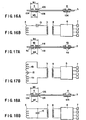
- FIG. 16A is a cross-sectional view of the same card substrate as is shown in FIGS. 3B, 8B and 12B.
- FIG. 16B shows an equivalent circuit of the card substrate shown in FIG. 16A.
- An antenna coil 4 realized as a wiring pattern using a conductive material is disposed on a peripheral portion of one surface of the substrate 5. Only one end of the antenna coil 4 is connected to one end of the second coupler coil 3, and the other end of the antenna coil 4 is opened.
- the other end of the second coupler coil 3 is guided to the other surface of the substrate 5 and connected to a conductor 104 formed of a conductive material on the other surface of the substrate 5 so as to be opposed to the antenna coil 4.
- a static capacitance is constituted by a pattern of conductive material forming the antenna coil 4 on the one surface, and the conductor 104 formed of conductive material on the other surface.
- a series capacitive element 15 in the equivalent circuit shown in FIG. 16B is obtained.
- the width Wa of the antenna coil 4 and the width Wb of the conductor 104 should not necessarily be made exactly equal, if a necessary static capacitance is obtained. However, it is desirable, as a minimum requirement, that end faces 108 of the conductor 104, the width between which is Wb, be disposed so as not to project out from end faces 106 of the antenna coil 4, the width between which is Wa. This can prevent a decrease in the coil area provided by the antenna coil 4.
- the number of turns of the antenna coil 4 is two.
- the number of turns of the antenna coil 4 and the pattern width thereof are determined in accordance with a necessary inductance and static capacitance. Since the other end of the antenna coil 4 can be opened at a desired location, the inductance of the antenna coil 4, the number of turns of which is one or more, can be adjusted by the length of the pattern of the antenna coil 4. On the other hand, needless to say, the area of the conductor 104 opposed to the antenna coil 4 can be freely set to obtain a necessary static capacitance. Therefore, compared to the conventional method in which the inductance of the coil can be adjusted only by the area of the coil and the number of turns thereof, the inductance and static capacitance can be easily adjusted.
- FIG. 17A is a cross-sectional view of the same card substrate as is shown in FIGS. 3B, 8B and 12B.
- FIG. 17B shows an equivalent circuit of the card substrate shown in FIG. 17A.
- a second antenna coil 4b realized as a wiring pattern using a conductive material is disposed on a peripheral portion of one surface of the substrate 5.
- One end of the second antenna coil 4b is connected to the second coupler coil 3, and the other end of the second antenna coil 4b is opened.
- the other end of the second coupler coil 3 is guided to the other surface of the substrate 5 and connected to one end of a first antenna coil 4a which is realized as a wiring pattern using a conductive material on the other surface of the substrate 5 so as to be opposed to the second antenna coil 4b.
- the other end of the first antenna coil 4a is disposed to be opened.
- a static capacitance is constituted by the pattern of conductive material forming the second antenna coil 4b on the one surface, and the pattern of conductive material forming the first antenna coil 4a on the other surface.
- the series capacitive element 15 in the equivalent circuit shown in FIG. 17B is obtained.
- the width Wc of the second antenna coil 4b and the width Wd of the first antenna coil 4a should not necessarily be made exactly equal, if a necessary static capacitance is obtained.
- the number of turns of the antenna coils 4a, 4b is two.
- the number of turns of the second antenna coil 4b and first antenna coil 4a, and the pattern widths thereof are determined in accordance with a necessary inductance and static capacitance. Since the other end of the second antenna coil 4b and the other end of the first antenna coil 4a can be opened at desired locations, the inductance of the second antenna coil 4b can be adjusted by the length of the pattern of the second antenna coil 4b and the inductance of the first antenna coil 4a can be adjusted by the length of the pattern of the first antenna coil 4a.
- the static capacitance increases in accordance with an area with which the second antenna coil 4b is opposed to the first antenna coil 4a, it is necessary to provide such an area with which the second antenna coil 4b is opposed to the first antenna coil 4a. Therefore, compared to the conventional method in which the inductance of the coil can be adjusted only by the area of the coil and the number of turns thereof, the inductance and static capacitance can be easily adjusted.
- FIG. 18A is a cross-sectional view of the same card substrate as is shown in FIGS. 3B, 8B and 12B.
- FIG. 18B shows an equivalent circuit of the card substrate shown in FIG. 18A.
- the antenna coil 4 realized as a wiring pattern using a conductive material is disposed on a peripheral portion of one surface of the substrate 5.
- One end of the antenna coil 4 is connected to one end of the second coupler coil 3, and the other end of the antenna coil 4 is connected to the other end of the second coupler coil 3.
- a conductor 124 using a conductor material is disposed on the other surface of the substrate 5 so as to be opposed to the antenna coil 4.
- the width We of the antenna coil 4 and the width Wf of the conductor 124 should not necessarily be made exactly equal, if a necessary static capacitance is obtained. However, it is desirable, as a minimum requirement, that end faces 128 of the conductor 124, the width between which is Wf, be disposed so as not to project out from end faces 126 of the antenna coil 4, the width between which is We. This can prevent a decrease in the coil area provided by the antenna coil 4.
- the number of turns of the antenna coil 4 is two.
- the number of turns of the antenna coil 4 and the pattern width thereof are determined in accordance with a necessary inductance and static capacitance.
Claims (7)
- Chipkarte, die sowohl die Funktion einer kontaktabhängigen als auch einer kontaktlosen Chipkarte besitzt und einen IC-Modul (2) und ein Antennenelement (3, 4) aufweist, wobei
der IC-Modul (2) einen IC-Chip (6), der eine kontaktabhängige Übertragungsfunktion und eine kontaktlose Übertragungsfunktion besitzt, und ein Modul-Substrat (9) mit einem als Kontakt-Übertragungselement dienenden externen Anschluss (7) und einer ersten Koppelspule (8) aufweist,
das Antennenelement (3, 4) eine Antenne (4) zur Durchführung eines Energieaufnahmevorgangs und/oder eines Sende-/Empfangsvorgangs in Wirkverbindung mit einem externen Lese-/Schreibgerät und eine mit der Antenne (4) verbundene zweite Koppelspule (3) aufweist,
der IC-Modul (2) in einer Ausnehmung (11) eines Kartensubstrates (10) derart angebracht ist, dass der externe Anschluss (7) außerhalb des Kartensubstrates (10) liegt und die erste Koppelspule (8) in der Ausnehmung (11) angeordnet ist, und
die erste Koppelspule (8) des IC-Moduls (2) und die zweite Koppelspule (3) des Antennenelements (3, 4) zur kontaktlosen Übertragung in enger Kopplung miteinander angeordnet sind und der IC-Modul (2) und das Antennenelement (3, 4) durch induktive Kopplung über die erste und die zweite Koppelspule (8, 3) kontaktlos miteinander gekoppelt sind, wobei
die Antenne (4) als geschlossene Schleife ausgebildet und die zweite Koppelspule (3) des Antennenelements (3, 4) außerhalb der Schleife der Antenne (4) angeordnet sind. - Chipkarte nach Anspruch 1, bei der das Antennenelement (4) ein kapazitives Element aufweist.
- Chipkarte nach Anspruch 1 oder 2, bei der ein Prägungsbereich (20) vorgesehen ist, wobei
der IC-Modul (2) in einem im wesentlichen mittleren Bereich einer kürzeren Seite der Karte und der Prägungsbereich (20) entlang einer längeren Seite der Karte angeordnet sind, und
die Antenne (4) zur kontaktlosen Übertragung derart angeordnet ist, dass keine Beeinträchtigung eines externen Anschlussbereiches (21) des IC-Moduls (2) und des Prägungsbereiches (20) auftritt. - Chipkarte nach Anspruch 1 oder 2, bei der ein Prägungsbereich (20) vorgesehen ist, wobei
der IC-Modul (2) in einem im wesentlichen mittleren Bereich einer kürzeren Seite der Karte und der Prägungsbereich (20) entlang einer längeren Seite der Karte angeordnet sind, und
die Antenne (4) zur kontaktlosen Übertragung derart angeordnet ist, dass keine Beeinträchtigung eines externen Anschlussbereiches (21) des IC-Moduls (2) und des Prägungsbereiches (20) auftritt, wobei die Antenne (4) in einem Bereich angeordnet ist, der von einer längeren Seite der Karte, die der einen längeren Seite gegenüberliegt, entlang der der Prägungsbereich (20) vorgesehen ist, der Grenze des Prägungsbereichs (20) an einer Innenseite der Karte, der Grenze des externen Anschlussbereiches (21) des IC-Moduls (2) an der Innenseite der Karte und einer kürzeren Seite der Karte definiert wird, die der einen kürzeren Seite gegenüberliegt, an der der IC-Modul (2) vorgesehen ist. - Chipkarte nach Anspruch 1 oder 2, bei der ein Prägungsbereich (20) vorgesehen ist, wobei
der IC-Modul (2) in einem im wesentlichen mittleren Bereich einer kürzeren Seite der Karte und der Prägungsbereich (20) entlang einer längeren Seite der Karte angeordnet sind, und
zumindest ein Teil der Antenne (4) zur kontaktlosen Übertragung zwischen dem Prägungsbereich (20) und einem Rand der Karte und zwischen einem externen Anschlussbereich (21) des IC-Moduls (2) und dem Rand der Karte entlang der Peripherie der Karte derart angeordnet ist, dass keine Beeinträchtigung des externen Anschlussbereiches (21) des IC-Moduls (2) und des Prägungsbereiches (20) auftritt. - Chipkarte nach Anspruch 1 oder 2, bei der ein Magnetstreifenbereich und ein Prägungsbereich (20) vorgesehen sind, wobei
der IC-Modul (2) in einem im wesentlichen mittleren Bereich einer kürzeren Seite der Karte, der Prägungsbereich (20) entlang einer längeren Seite der Karte und der Magnetstreifenbereich entlang der anderen längeren Seite der Karte angeordnet sind, und
die Antenne (4) zur kontaktlosen Übertragung derart angeordnet ist, dass keine Beeinträchtigung eines externen Anschlussbereiches (21) des IC-Moduls (2), des Prägungsbereiches (20) und des Magnetstreifenbereiches auftritt. - Chipkarte nach Anspruch 1 oder 2, bei der ein Magnetstreifenbereich und ein Prägungsbereich (20) vorgesehen sind, wobei
der IC-Modul (2) in einem im wesentlichen mittleren Bereich einer kürzeren Seite der Karte, der Prägungsbereich (20) entlang einer längeren Seite der Karte und der Magnetstreifenbereich entlang der anderen längeren Seite der Karte angeordnet sind, und
die Antenne (4) zur kontaktlosen Übertragung in einem Bereich, der von der Grenze des Prägungsbereichs (20) an einer Innenseite der Karte, der Grenze eines externen Anschlussbereiches (21) des IC-Moduls (2) an der Innenseite der Karte, der Grenze des Magnetstreifenbereiches an der Innenseite der Karte und der der einen kürzeren Seite mit dem IC-Modul (2) gegenüberliegenden kürzeren Seite definiert wird, derart angeordnet ist, dass keine Beeinträchtigung des externen Anschlussbereiches (21) des IC-Moduls (2), des Prägungsbereiches (20) und des Magnetstreifenbereiches auftritt.
Applications Claiming Priority (7)
| Application Number | Priority Date | Filing Date | Title |
|---|---|---|---|
| JP31394597A JP3800765B2 (ja) | 1997-11-14 | 1997-11-14 | 複合icカード |
| JP31394497A JPH11149536A (ja) | 1997-11-14 | 1997-11-14 | 複合icカード |
| JP31394697A JP3800766B2 (ja) | 1997-11-14 | 1997-11-14 | 複合icモジュールおよび複合icカード |
| JP31394497 | 1997-11-14 | ||
| JP31394597 | 1997-11-14 | ||
| JP31394697 | 1997-11-14 | ||
| PCT/JP1998/005142 WO1999026195A1 (fr) | 1997-11-14 | 1998-11-16 | Module ci composite et carte ci composite |
Publications (3)
| Publication Number | Publication Date |
|---|---|
| EP1031939A1 EP1031939A1 (de) | 2000-08-30 |
| EP1031939A4 EP1031939A4 (de) | 2002-11-06 |
| EP1031939B1 true EP1031939B1 (de) | 2005-09-14 |
Family
ID=27339370
Family Applications (1)
| Application Number | Title | Priority Date | Filing Date |
|---|---|---|---|
| EP98953057A Expired - Lifetime EP1031939B1 (de) | 1997-11-14 | 1998-11-16 | Zusammengesetzte ic-karte |
Country Status (5)
| Country | Link |
|---|---|
| US (1) | US6378774B1 (de) |
| EP (1) | EP1031939B1 (de) |
| CN (1) | CN1179295C (de) |
| DE (1) | DE69831592T2 (de) |
| WO (1) | WO1999026195A1 (de) |
Cited By (14)
| Publication number | Priority date | Publication date | Assignee | Title |
|---|---|---|---|---|
| WO2011023604A1 (fr) | 2009-08-28 | 2011-03-03 | Gemalto Sa | Dispositif a antenne relais, dispositif radiofrequence associe et procede de realisation |
| WO2011023570A1 (fr) | 2009-08-28 | 2011-03-03 | Gemalto Sa | Procede de realisation d'un dispositif comprenant un circuit radiofrequence, et dispositif obtenu |
| US8100337B2 (en) | 2005-08-30 | 2012-01-24 | Smart Packaging Soultions (SPS) | Double interface communication electronic module, in particular for a chip card |
| EP2541471A1 (de) | 2011-07-01 | 2013-01-02 | Gemalto SA | Tragbare Vorrichtung mit ausgesparten elektrischen Kontakten |
| EP2710523B1 (de) | 2011-05-17 | 2016-08-17 | Gemalto SA | Hochfrequenz-transponder mit passiver resonanzschaltung |
| US10248902B1 (en) | 2017-11-06 | 2019-04-02 | Féinics Amatech Teoranta | Coupling frames for RFID devices |
| EP3663983A1 (de) | 2018-12-06 | 2020-06-10 | Thales Dis France SA | Herstellungsverfahren einer metallischen oder nichtmetallischen chipkarte mit relaisantenne |
| EP3671563A1 (de) | 2018-12-21 | 2020-06-24 | Thales Dis France SA | Herstellungsverfahren einer metallischen chipkarte, bevorzugt mit relaisantenne |
| EP3789919A1 (de) | 2019-09-09 | 2021-03-10 | Thales Dis France SA | Herstellungsverfahren einer metallischen chipkarte mit minirelais-antenne |
| EP3832546A1 (de) | 2019-12-02 | 2021-06-09 | Thales Dis France Sa | Herstellungsverfahren einer funkfrequenz-chipkarte, die eine metallplatte mit einem schlitz oder einem spiel in der platte umfasst |
| EP3832547A1 (de) | 2019-12-02 | 2021-06-09 | Thales Dis France Sa | Die erfindung betrifft ein herstellungsverfahren einer funkfrequenz-chipkarte, die eine metallplatte mit einem schlitz in der platte umfasst |
| DE102013103365B4 (de) | 2012-04-05 | 2022-02-03 | Infineon Technologies Ag | Datenträger zur kontaktlosen Datenübertragung und Verfahren zur Herstellung eines solchen Datenträgers |
| RU2797652C1 (ru) * | 2019-09-09 | 2023-06-07 | Таль Дис Франс Сас | Способ изготовления металлической смарт-карты с релейной мини-антенной |
| US11928537B2 (en) | 2013-01-18 | 2024-03-12 | Amatech Group Limited | Manufacturing metal inlays for dual interface metal cards |
Families Citing this family (334)
| Publication number | Priority date | Publication date | Assignee | Title |
|---|---|---|---|---|
| IL122250A (en) * | 1997-11-19 | 2003-07-31 | On Track Innovations Ltd | Smart card amenable to assembly using two manufacturing stages and a method of manufacture thereof |
| EP0977145A3 (de) * | 1998-07-28 | 2002-11-06 | Kabushiki Kaisha Toshiba | Radio IC-Karte |
| US6837438B1 (en) * | 1998-10-30 | 2005-01-04 | Hitachi Maxell, Ltd. | Non-contact information medium and communication system utilizing the same |
| US6577229B1 (en) * | 1999-06-10 | 2003-06-10 | Cubic Corporation | Multiple protocol smart card communication device |
| DE10006816C2 (de) * | 2000-02-15 | 2003-03-13 | Sokymat Id Component Gmbh | Transponder-Vorrichtung zur Identifikation von Objekten gegenüber Einrichtungen |
| JP4239352B2 (ja) * | 2000-03-28 | 2009-03-18 | 株式会社日立製作所 | 電子装置の製造方法 |
| FR2811108B1 (fr) * | 2000-06-29 | 2002-09-27 | A S K | Dispositif peripherique d'affichage sans contact pour objet portable sans contact |
| DE10032128A1 (de) * | 2000-07-05 | 2002-01-17 | Giesecke & Devrient Gmbh | Sicherheitspapier und daraus hergestelltes Wertdokument |
| US20030169169A1 (en) * | 2000-08-17 | 2003-09-11 | Luc Wuidart | Antenna generating an electromagnetic field for transponder |
| EP1195714A1 (de) * | 2000-10-04 | 2002-04-10 | Sokymat S.A. | Transpondereinheit |
| US6634564B2 (en) * | 2000-10-24 | 2003-10-21 | Dai Nippon Printing Co., Ltd. | Contact/noncontact type data carrier module |
| US6628240B2 (en) * | 2000-11-08 | 2003-09-30 | American Pacific Technology | Method and apparatus for rapid staking of antennae in smart card manufacture |
| JP3468227B2 (ja) * | 2001-04-18 | 2003-11-17 | 株式会社村田製作所 | スイッチング電源モジュール |
| JP2002342731A (ja) | 2001-05-16 | 2002-11-29 | Matsushita Electric Ind Co Ltd | 複合icカード |
| FI112550B (fi) * | 2001-05-31 | 2003-12-15 | Rafsec Oy | Älytarra ja älytarraraina |
| US7150406B2 (en) * | 2001-09-18 | 2006-12-19 | Nagraid S.A. | Thin electronic label and method for making same |
| DE60228636D1 (de) * | 2001-11-21 | 2008-10-09 | Mineral Lassen Llc | Zusammenschaltung drahtloser Kommunikationsvorrichtungen |
| EP1315234A1 (de) * | 2001-11-26 | 2003-05-28 | Eta SA Fabriques d'Ebauches | VHF-Empfangsantenne integriert in das Armband einer tragbaren elektronischen Vorrichtung |
| AU2003212915A1 (en) * | 2002-02-04 | 2003-09-02 | Raytheon Company | Enhancement antenna for article identification |
| US7344074B2 (en) * | 2002-04-08 | 2008-03-18 | Nokia Corporation | Mobile terminal featuring smart card interrupt |
| JP4058300B2 (ja) * | 2002-06-21 | 2008-03-05 | 株式会社日立製作所 | 携帯情報装置 |
| GB2393076A (en) | 2002-09-12 | 2004-03-17 | Rf Tags Ltd | Radio frequency identification tag which has a ground plane not substantially larger than the area spanned by the patch antenna |
| KR20040038134A (ko) * | 2002-10-31 | 2004-05-08 | 주식회사 쓰리비 시스템 | 안정된 비접촉 통신수단을 제공하는 콤비형 스마트 카드 |
| DE10258670A1 (de) * | 2002-12-13 | 2004-06-24 | Giesecke & Devrient Gmbh | Transponder zur berührungslosen Übertragung von Daten |
| DE10258511A1 (de) * | 2002-12-14 | 2004-07-08 | Infineon Technologies Ag | Integrierte Schaltung sowie zugehörige gehäuste integrierte Schaltung |
| JP4241147B2 (ja) * | 2003-04-10 | 2009-03-18 | ソニー株式会社 | Icカードの製造方法 |
| US20040243267A1 (en) * | 2003-05-30 | 2004-12-02 | Shih-Wen Tu | Systematic control of cross fabrication (fab) engineering changes in integrated circuit (IC) foundry manufacturing |
| US20040242270A1 (en) * | 2003-06-02 | 2004-12-02 | Endicott Interconnect Technologies, Inc. | Electronic card |
| US7013365B2 (en) * | 2003-06-16 | 2006-03-14 | Michael Arnouse | System of secure personal identification, information processing, and precise point of contact location and timing |
| WO2005017821A1 (ja) * | 2003-08-13 | 2005-02-24 | Murata Manufacturing Co., Ltd. | リーダライタ及び移動体通信装置 |
| JP3982476B2 (ja) * | 2003-10-01 | 2007-09-26 | ソニー株式会社 | 通信システム |
| US7163155B2 (en) * | 2003-11-05 | 2007-01-16 | Interdigital Technology Corporation | ASIC-embedded switchable antenna arrays |
| DE10356153B4 (de) * | 2003-12-02 | 2010-01-14 | Infineon Technologies Ag | Modul für kontaktlose Chipkarten oder Identifizierungssysteme |
| TW200525654A (en) * | 2003-12-26 | 2005-08-01 | Toray Eng Co Ltd | Electronic circuit board intermediate member, manufacturing method therefor, manufacturing equipment therefor, method for manufacturing noncontact ID card and the like, and equipment therefor |
| ATE441901T1 (de) | 2004-02-04 | 2009-09-15 | Bibliotheca Rfid Library Syste | Resonanzetikette zur anbringung an einem mit einer metallisierung versehenen datenträger |
| DE102004021872B3 (de) * | 2004-05-04 | 2005-12-22 | Infineon Technologies Ag | Chipkarte, Verfahren zum Herstellen einer Chipkarte und elektrisch leitfähiges Kontaktierungselement |
| US7834743B2 (en) * | 2004-06-10 | 2010-11-16 | Panasonic Corporation | RFID tag and RFID tag communication distance modification method |
| US7274297B2 (en) | 2004-07-01 | 2007-09-25 | Intermec Ip Corp. | RFID tag and method of manufacture |
| US7158033B2 (en) * | 2004-09-01 | 2007-01-02 | Avery Dennison Corporation | RFID device with combined reactive coupler |
| US20060044769A1 (en) * | 2004-09-01 | 2006-03-02 | Forster Ian J | RFID device with magnetic coupling |
| JP4169158B2 (ja) * | 2004-12-24 | 2008-10-22 | インターナショナル・ビジネス・マシーンズ・コーポレーション | 無線icチップおよびこれを用いた位置認識システム並びにセキュリティシステム |
| JP2006179766A (ja) * | 2004-12-24 | 2006-07-06 | Mitsubishi Electric Corp | パワーモジュールおよびその製造方法 |
| JP4473141B2 (ja) * | 2005-01-04 | 2010-06-02 | 日立オートモティブシステムズ株式会社 | 電子制御装置 |
| WO2006107862A2 (en) * | 2005-04-04 | 2006-10-12 | Mastercard International Incorporated | A system and method enabling fourth line embossing on contactless cards |
| KR20080003006A (ko) * | 2005-04-27 | 2008-01-04 | 프라이베이시스, 인크. | 전자 카드 및 그의 제조방법 |
| US20060244575A1 (en) * | 2005-04-29 | 2006-11-02 | Nick Ramirez | Key-less control apparatus for motor vehicles |
| US8477020B2 (en) | 2005-04-29 | 2013-07-02 | Heistproof, Llc | Remote ignition, theft detterence, and records keeping system for a vehicle |
| US8325026B2 (en) * | 2005-04-29 | 2012-12-04 | Heistproof, Llc | Remote ignition, theft deterrence, and records keeping system for a vehicle |
| US7060611B1 (en) * | 2005-06-10 | 2006-06-13 | Ycl Mechanical Co., Ltd. | Method for manufacturing electric device for signal transmission |
| EP1910872B1 (de) * | 2005-07-28 | 2011-06-29 | Tagsys SAS | Zwei abgestimmte schaltkreise enthaltendes rfid-etikett |
| RU2008110177A (ru) * | 2005-08-18 | 2009-09-27 | АйВиАй СМАРТ ТЕКНОЛОДЖИЗ, ИНК. (US) | Система и способ биометрической аутентификации |
| US20110133896A1 (en) * | 2007-10-17 | 2011-06-09 | Bae Systems Information And Electronic Systems Integration Inc. | Methods For Coupling An RFID Chip To An Antenna |
| DE102005042444B4 (de) * | 2005-09-06 | 2007-10-11 | Ksw Microtec Ag | Anordnung für eine RFID - Transponder - Antenne |
| WO2007033706A1 (de) * | 2005-09-24 | 2007-03-29 | Dräger Medical AG & Co. KG | Mehrteiliges medizintechnisches system mit einem überbrückungselement |
| WO2007037578A1 (en) * | 2005-09-29 | 2007-04-05 | Electronics And Telecommunications Research Institute | Antenna with high isolation |
| FR2893162B1 (fr) * | 2005-11-08 | 2008-02-15 | Oberthur Card Syst Sa | Carte a microcircuit comportant un condensateur avantageusement interdigital |
| FR2893163B1 (fr) * | 2005-11-08 | 2008-02-01 | Oberthur Card Syst Sa | Procede de fabrication d'une carte a microcircuit et carte a microcircuit, notamment a antenne magnetique. |
| US7519328B2 (en) | 2006-01-19 | 2009-04-14 | Murata Manufacturing Co., Ltd. | Wireless IC device and component for wireless IC device |
| EP2375495A1 (de) * | 2006-01-19 | 2011-10-12 | Murata Manufacturing Co., Ltd. | Drahtlose integrierte Schaltung |
| FR2899000B1 (fr) * | 2006-03-24 | 2008-10-17 | Arjowiggins Security Soc Par A | Dispositif radiofrequence comportant un composant electronique pourvu d'une antenne integree et couplee electromagnetiquement a une antenne d'amplification |
| JP4235686B2 (ja) * | 2006-03-30 | 2009-03-11 | 王子製紙株式会社 | Icモジュール、icインレット及びic実装体 |
| KR100999731B1 (ko) * | 2006-03-31 | 2010-12-08 | 가부시키가이샤 히타치세이사쿠쇼 | 전자 태그 |
| DE112007000799B4 (de) | 2006-04-10 | 2013-10-10 | Murata Mfg. Co., Ltd. | Drahtlose IC-Vorrichtung |
| JP4572983B2 (ja) | 2006-04-14 | 2010-11-04 | 株式会社村田製作所 | 無線icデバイス |
| CN102780085A (zh) * | 2006-04-14 | 2012-11-14 | 株式会社村田制作所 | 天线 |
| EP2012388B1 (de) * | 2006-04-26 | 2011-12-28 | Murata Manufacturing Co. Ltd. | Mit speiseleiterplatte versehener gegenstand |
| US9064198B2 (en) | 2006-04-26 | 2015-06-23 | Murata Manufacturing Co., Ltd. | Electromagnetic-coupling-module-attached article |
| IL175824A0 (en) * | 2006-05-22 | 2007-09-20 | On Track Innovations Ltd | Data transaction card having a tunable coil antenna with reduced footprint |
| WO2007138919A1 (ja) | 2006-05-26 | 2007-12-06 | Murata Manufacturing Co., Ltd. | データ結合器 |
| CN101454989A (zh) * | 2006-05-30 | 2009-06-10 | 株式会社村田制作所 | 信息终端设备 |
| JP4775440B2 (ja) | 2006-06-01 | 2011-09-21 | 株式会社村田製作所 | 無線icデバイス及び無線icデバイス用複合部品 |
| JP4983794B2 (ja) * | 2006-06-12 | 2012-07-25 | 株式会社村田製作所 | 電磁結合モジュール、無線icデバイスの検査システム及びそれを用いた電磁結合モジュール、無線icデバイスの製造方法 |
| US8338930B2 (en) * | 2006-06-21 | 2012-12-25 | Broadcom Corporation | Integrated circuit with electromagnetic intrachip communication and methods for use therewith |
| EP1870797B2 (de) * | 2006-06-23 | 2020-10-07 | ASTRA Gesellschaft für Asset Management mbH & Co. KG | Informationsträger für Textilien |
| CN101467209B (zh) * | 2006-06-30 | 2012-03-21 | 株式会社村田制作所 | 光盘 |
| WO2008007606A1 (fr) * | 2006-07-11 | 2008-01-17 | Murata Manufacturing Co., Ltd. | Dispositif à antenne et circuit résonnant |
| US7999383B2 (en) | 2006-07-21 | 2011-08-16 | Bae Systems Information And Electronic Systems Integration Inc. | High speed, high density, low power die interconnect system |
| JP4310589B2 (ja) | 2006-08-24 | 2009-08-12 | 株式会社村田製作所 | 無線icデバイスの検査システム及びそれを用いた無線icデバイスの製造方法 |
| FR2893164B1 (fr) * | 2006-08-31 | 2012-09-28 | Oberthur Card Syst Sa | Procede de fabrication d'une carte a micro-circuit, notamment a antenne magnetique. |
| JP5052079B2 (ja) * | 2006-09-08 | 2012-10-17 | 株式会社半導体エネルギー研究所 | センサ装置及びそれを有する容器類 |
| US20100006655A1 (en) * | 2006-09-08 | 2010-01-14 | Simon Phillips | Sub-card personalization process using temporary antenna |
| WO2008050535A1 (fr) | 2006-09-26 | 2008-05-02 | Murata Manufacturing Co., Ltd. | Module couplé électromagnétiquement et article muni de celui-ci |
| CN101523750B (zh) * | 2006-10-27 | 2016-08-31 | 株式会社村田制作所 | 带电磁耦合模块的物品 |
| DE102006052517A1 (de) * | 2006-11-06 | 2008-05-08 | Bielomatik Leuze Gmbh + Co.Kg | Chipmodul für ein RFID-System |
| DE102006062308A1 (de) * | 2006-12-27 | 2008-07-17 | ASTRA Gesellschaft für Asset Management mbH & Co. KG | Passives Detektierplättchen |
| JP4835696B2 (ja) | 2007-01-26 | 2011-12-14 | 株式会社村田製作所 | 電磁結合モジュール付き容器 |
| JP4888494B2 (ja) | 2007-02-06 | 2012-02-29 | 株式会社村田製作所 | 電磁結合モジュール付き包装材 |
| JPWO2008096574A1 (ja) * | 2007-02-06 | 2010-05-20 | 株式会社村田製作所 | 電磁結合モジュール付き包装材 |
| FR2915011B1 (fr) | 2007-03-29 | 2009-06-05 | Smart Packaging Solutions Sps | Carte a puce a double interface de communication |
| US8009101B2 (en) | 2007-04-06 | 2011-08-30 | Murata Manufacturing Co., Ltd. | Wireless IC device |
| EP2133827B1 (de) | 2007-04-06 | 2012-04-25 | Murata Manufacturing Co. Ltd. | Funk-ic-vorrichtung |
| JP4697332B2 (ja) * | 2007-04-09 | 2011-06-08 | 株式会社村田製作所 | 無線icデバイス |
| US7762472B2 (en) | 2007-07-04 | 2010-07-27 | Murata Manufacturing Co., Ltd | Wireless IC device |
| US8235299B2 (en) | 2007-07-04 | 2012-08-07 | Murata Manufacturing Co., Ltd. | Wireless IC device and component for wireless IC device |
| FR2915010B1 (fr) * | 2007-04-16 | 2009-06-05 | Smart Packaging Solutions Sps | Module microelectronique a double interface de communication notamment pour carte a puce. |
| HK1109708A2 (en) * | 2007-04-24 | 2008-06-13 | On Track Innovations Ltd | Interface card and apparatus and process for the formation thereof |
| ATE540377T1 (de) * | 2007-04-26 | 2012-01-15 | Murata Manufacturing Co | Drahtlose ic-vorrichtung |
| ATE544129T1 (de) * | 2007-04-27 | 2012-02-15 | Murata Manufacturing Co | Drahtlose ic-vorrichtung |
| WO2008136220A1 (ja) | 2007-04-27 | 2008-11-13 | Murata Manufacturing Co., Ltd. | 無線icデバイス |
| CN101568934A (zh) | 2007-05-10 | 2009-10-28 | 株式会社村田制作所 | 无线ic器件 |
| JP4666102B2 (ja) | 2007-05-11 | 2011-04-06 | 株式会社村田製作所 | 無線icデバイス |
| DE102007022615A1 (de) * | 2007-05-15 | 2008-11-20 | Infineon Technologies Ag | Kontaktloses Übertragungssystem und Verfahren zum Herstellen desselben |
| DE102007029083B4 (de) * | 2007-06-21 | 2019-05-16 | ASTRA Gesellschaft für Asset Management mbH & Co. KG | Kartendatenträger mit Detektierplättchen |
| EP2077602B1 (de) * | 2007-06-27 | 2012-02-08 | Murata Manufacturing Co. Ltd. | Kabelloses ic-gerät |
| IL184260A0 (en) * | 2007-06-27 | 2008-03-20 | On Track Innovations Ltd | Mobile telecommunications device having sim/antenna coil interface |
| CN104078767B (zh) * | 2007-07-09 | 2015-12-09 | 株式会社村田制作所 | 无线ic器件 |
| EP2166490B1 (de) * | 2007-07-17 | 2015-04-01 | Murata Manufacturing Co. Ltd. | Drahtlose ic-vorrichtung und elektronische vorrichtung |
| EP2166616B1 (de) * | 2007-07-18 | 2013-11-27 | Murata Manufacturing Co. Ltd. | Drahtlose ic-vorrichtung |
| CN101578736B (zh) * | 2007-07-18 | 2013-02-27 | 株式会社村田制作所 | 无线ic器件 |
| JP4434311B2 (ja) | 2007-07-18 | 2010-03-17 | 株式会社村田製作所 | 無線icデバイスおよびその製造方法 |
| US20090021352A1 (en) * | 2007-07-18 | 2009-01-22 | Murata Manufacturing Co., Ltd. | Radio frequency ic device and electronic apparatus |
| US7830311B2 (en) | 2007-07-18 | 2010-11-09 | Murata Manufacturing Co., Ltd. | Wireless IC device and electronic device |
| JP5155616B2 (ja) * | 2007-07-25 | 2013-03-06 | 沖プリンテッドサーキット株式会社 | Rfidタグ、rfidシステムおよびrfidタグの製造方法 |
| FR2919409B1 (fr) | 2007-07-26 | 2009-09-04 | Smart Packaging Solutions Sps | Document securise a puce sans contact avec protection des donnees contre les lectures non autorisees. |
| US7973722B1 (en) | 2007-08-28 | 2011-07-05 | Apple Inc. | Electronic device with conductive housing and near field antenna |
| EP2045872B1 (de) * | 2007-10-03 | 2011-08-10 | Assa Abloy Ab | Kopplungsvorrichtung für einen Transponder und Chipkarte mit derartiger Vorrichtung |
| US8028923B2 (en) * | 2007-11-14 | 2011-10-04 | Smartrac Ip B.V. | Electronic inlay structure and method of manufacture thereof |
| US20090123743A1 (en) * | 2007-11-14 | 2009-05-14 | Guy Shafran | Method of manufacture of wire imbedded inlay |
| JP5403903B2 (ja) | 2007-12-04 | 2014-01-29 | ルネサスエレクトロニクス株式会社 | 半導体装置、その製造方法、および当該半導体装置を用いた信号送受信方法 |
| US20090145971A1 (en) * | 2007-12-07 | 2009-06-11 | Wen Cheng Yin | Printed wireless rf identification label structure |
| EP2408064B1 (de) | 2007-12-20 | 2020-08-05 | Murata Manufacturing Co., Ltd. | Drahtlose integrierte Schaltung |
| US20090159682A1 (en) | 2007-12-24 | 2009-06-25 | Dynamics Inc. | Cards and devices with multi-function magnetic emulators and methods for using same |
| JP4561931B2 (ja) * | 2007-12-26 | 2010-10-13 | 株式会社村田製作所 | アンテナ装置および無線icデバイス |
| WO2009110382A1 (ja) * | 2008-03-03 | 2009-09-11 | 株式会社村田製作所 | 複合アンテナ |
| JP5267463B2 (ja) | 2008-03-03 | 2013-08-21 | 株式会社村田製作所 | 無線icデバイス及び無線通信システム |
| CN101978383B (zh) * | 2008-03-20 | 2016-03-23 | 国泰银恩企业有限责任公司 | 用于无接触通信的收发电路和包括这种收发电路的nfc设备或rfid读/写设备 |
| WO2009119548A1 (ja) * | 2008-03-26 | 2009-10-01 | 株式会社村田製作所 | 無線icデバイス |
| CN101953025A (zh) * | 2008-04-14 | 2011-01-19 | 株式会社村田制作所 | 无线ic器件、电子设备以及无线ic器件的谐振频率调整方法 |
| EP2269159A1 (de) * | 2008-04-16 | 2011-01-05 | FOSS Analytical A/S | Drahtloser informationsträger |
| JP4609604B2 (ja) | 2008-05-21 | 2011-01-12 | 株式会社村田製作所 | 無線icデバイス |
| WO2009142068A1 (ja) * | 2008-05-22 | 2009-11-26 | 株式会社村田製作所 | 無線icデバイス及びその製造方法 |
| WO2009142756A2 (en) * | 2008-05-22 | 2009-11-26 | California Institute Of Technology | On-chip highly-efficient antennas using strong resonant coupling |
| EP2290586B1 (de) * | 2008-05-26 | 2014-06-25 | Murata Manufacturing Co., Ltd. | Drahtloses ic-gerätesystem und verfahren zur authentifizierung eines drahtlosen ic-geräts |
| JP4535210B2 (ja) * | 2008-05-28 | 2010-09-01 | 株式会社村田製作所 | 無線icデバイス用部品および無線icデバイス |
| JP4557186B2 (ja) | 2008-06-25 | 2010-10-06 | 株式会社村田製作所 | 無線icデバイスとその製造方法 |
| JP4671001B2 (ja) * | 2008-07-04 | 2011-04-13 | 株式会社村田製作所 | 無線icデバイス |
| US9104899B2 (en) * | 2008-08-13 | 2015-08-11 | Infineon Technologies Ag | Multiple transceivers operable as a single transceiver |
| WO2010021217A1 (ja) * | 2008-08-19 | 2010-02-25 | 株式会社村田製作所 | 無線icデバイス及びその製造方法 |
| US20100090008A1 (en) * | 2008-10-13 | 2010-04-15 | Oded Bashan | Authentication seal |
| WO2010047214A1 (ja) * | 2008-10-24 | 2010-04-29 | 株式会社村田製作所 | 無線icデバイス |
| US20100102131A1 (en) * | 2008-10-28 | 2010-04-29 | First Data Corporation | Systems and Methods for Disabling a Contactless Transaction Device |
| WO2010050361A1 (ja) * | 2008-10-29 | 2010-05-06 | 株式会社村田製作所 | 無線icデバイス |
| DE112009002384B4 (de) * | 2008-11-17 | 2021-05-06 | Murata Manufacturing Co., Ltd. | Antenne und Drahtlose-IC-Bauelement |
| WO2010066955A1 (fr) | 2008-12-11 | 2010-06-17 | Yves Eray | Circuit d'antenne rfid |
| WO2010079830A1 (ja) | 2009-01-09 | 2010-07-15 | 株式会社村田製作所 | 無線icデバイス、無線icモジュール、および無線icモジュールの製造方法 |
| WO2010082413A1 (ja) * | 2009-01-16 | 2010-07-22 | 株式会社村田製作所 | 高周波デバイス及び無線icデバイス |
| EP2385580B1 (de) * | 2009-01-30 | 2014-04-09 | Murata Manufacturing Co., Ltd. | Antenne und drahtlose ic-vorrichtung |
| JP5510450B2 (ja) | 2009-04-14 | 2014-06-04 | 株式会社村田製作所 | 無線icデバイス |
| WO2010122685A1 (ja) | 2009-04-21 | 2010-10-28 | 株式会社村田製作所 | アンテナ装置及びその共振周波数設定方法 |
| CN102449846B (zh) | 2009-06-03 | 2015-02-04 | 株式会社村田制作所 | 无线ic器件及其制造方法 |
| US8422973B2 (en) * | 2009-06-16 | 2013-04-16 | B & Plus K.K. | Bidirectional transmission coil and bidirectional transmission system using the same |
| KR100951620B1 (ko) * | 2009-06-19 | 2010-04-09 | 한국조폐공사 | 콤비카드 및 콤비카드 통신 장치 |
| WO2010146944A1 (ja) | 2009-06-19 | 2010-12-23 | 株式会社村田製作所 | 無線icデバイス及び給電回路と放射板との結合方法 |
| US8593256B2 (en) * | 2009-06-23 | 2013-11-26 | Avery Dennison Corporation | Washable RFID device for apparel tracking |
| CN102474009B (zh) | 2009-07-03 | 2015-01-07 | 株式会社村田制作所 | 天线及天线模块 |
| WO2011037234A1 (ja) | 2009-09-28 | 2011-03-31 | 株式会社村田製作所 | 無線icデバイスおよびそれを用いた環境状態検出方法 |
| JP5201270B2 (ja) | 2009-09-30 | 2013-06-05 | 株式会社村田製作所 | 回路基板及びその製造方法 |
| JP5304580B2 (ja) * | 2009-10-02 | 2013-10-02 | 株式会社村田製作所 | 無線icデバイス |
| US8366009B2 (en) | 2010-08-12 | 2013-02-05 | Féinics Amatech Teoranta | Coupling in and to RFID smart cards |
| US8474726B2 (en) | 2010-08-12 | 2013-07-02 | Feinics Amatech Teoranta | RFID antenna modules and increasing coupling |
| US9165240B2 (en) * | 2009-10-15 | 2015-10-20 | Feinics Amatech Teoranta | Coupling in and to RFID smart cards |
| WO2011045970A1 (ja) | 2009-10-16 | 2011-04-21 | 株式会社村田製作所 | アンテナ及び無線icデバイス |
| JP5418600B2 (ja) | 2009-10-27 | 2014-02-19 | 株式会社村田製作所 | 送受信装置及び無線タグ読み取り装置 |
| WO2011055701A1 (ja) | 2009-11-04 | 2011-05-12 | 株式会社村田製作所 | 通信端末及び情報処理システム |
| WO2011055702A1 (ja) | 2009-11-04 | 2011-05-12 | 株式会社村田製作所 | 無線icタグ、リーダライタ及び情報処理システム |
| JP5327334B2 (ja) | 2009-11-04 | 2013-10-30 | 株式会社村田製作所 | 通信端末及び情報処理システム |
| GB2487491B (en) | 2009-11-20 | 2014-09-03 | Murata Manufacturing Co | Antenna device and mobile communication terminal |
| JP4978756B2 (ja) | 2009-12-24 | 2012-07-18 | 株式会社村田製作所 | 通信端末 |
| WO2011108340A1 (ja) | 2010-03-03 | 2011-09-09 | 株式会社村田製作所 | 無線通信モジュール及び無線通信デバイス |
| JP5403146B2 (ja) | 2010-03-03 | 2014-01-29 | 株式会社村田製作所 | 無線通信デバイス及び無線通信端末 |
| WO2011111509A1 (ja) | 2010-03-12 | 2011-09-15 | 株式会社村田製作所 | 無線通信デバイス及び金属製物品 |
| WO2011118379A1 (ja) * | 2010-03-24 | 2011-09-29 | 株式会社村田製作所 | Rfidシステム |
| JP5630499B2 (ja) | 2010-03-31 | 2014-11-26 | 株式会社村田製作所 | アンテナ装置及び無線通信デバイス |
| DE102010028926A1 (de) * | 2010-05-12 | 2011-11-17 | Bundesdruckerei Gmbh | Dokument und Verfahren zur Herstellung eines Dokuments |
| JP5299351B2 (ja) | 2010-05-14 | 2013-09-25 | 株式会社村田製作所 | 無線icデバイス |
| JP5170156B2 (ja) | 2010-05-14 | 2013-03-27 | 株式会社村田製作所 | 無線icデバイス |
| US8195236B2 (en) | 2010-06-16 | 2012-06-05 | On Track Innovations Ltd. | Retrofit contactless smart SIM functionality in mobile communicators |
| WO2012005278A1 (ja) | 2010-07-08 | 2012-01-12 | 株式会社村田製作所 | アンテナ及びrfidデバイス |
| FR2963139B1 (fr) * | 2010-07-20 | 2012-09-14 | Oberthur Technologies | Dispositif a microcircuit comprenant des moyens d'amplification du gain d'une antenne |
| CN104752813B (zh) | 2010-07-28 | 2018-03-02 | 株式会社村田制作所 | 天线装置及通信终端设备 |
| KR20120011974A (ko) * | 2010-07-29 | 2012-02-09 | 삼성전자주식회사 | 복수 개의 인터페이스를 지원하는 스마트 카드 및 그것의 인터페이스 방법 |
| JP5423897B2 (ja) | 2010-08-10 | 2014-02-19 | 株式会社村田製作所 | プリント配線板及び無線通信システム |
| IT1401521B1 (it) * | 2010-08-11 | 2013-07-26 | St Microelectronics Srl | Sistema di sicurezza per almeno un circuito integrato ic, scheda a circuito integrato in sicurezza e metodo di comunicazione wireless in sicurezza. |
| US8870080B2 (en) | 2010-08-12 | 2014-10-28 | Féinics Amatech Teoranta | RFID antenna modules and methods |
| WO2013020971A1 (en) | 2011-08-08 | 2013-02-14 | Féinics Amatech Teoranta | Improving coupling in and to rfid smart cards |
| US8789762B2 (en) | 2010-08-12 | 2014-07-29 | Feinics Amatech Teoranta | RFID antenna modules and methods of making |
| US9195932B2 (en) | 2010-08-12 | 2015-11-24 | Féinics Amatech Teoranta | Booster antenna configurations and methods |
| US9633304B2 (en) * | 2010-08-12 | 2017-04-25 | Féinics Amatech Teoranta | Booster antenna configurations and methods |
| US9112272B2 (en) | 2010-08-12 | 2015-08-18 | Feinics Amatech Teoranta | Antenna modules for dual interface smart cards, booster antenna configurations, and methods |
| US8991712B2 (en) | 2010-08-12 | 2015-03-31 | Féinics Amatech Teoranta | Coupling in and to RFID smart cards |
| US9033250B2 (en) | 2010-08-12 | 2015-05-19 | Féinics Amatech Teoranta | Dual interface smart cards, and methods of manufacturing |
| JP5234071B2 (ja) | 2010-09-03 | 2013-07-10 | 株式会社村田製作所 | Rficモジュール |
| WO2012043432A1 (ja) | 2010-09-30 | 2012-04-05 | 株式会社村田製作所 | 無線icデバイス |
| CN103053074B (zh) | 2010-10-12 | 2015-10-21 | 株式会社村田制作所 | 天线装置及通信终端装置 |
| GB2501385B (en) | 2010-10-21 | 2015-05-27 | Murata Manufacturing Co | Communication terminal device |
| US8424757B2 (en) | 2010-12-06 | 2013-04-23 | On Track Innovations Ltd. | Contactless smart SIM functionality retrofit for mobile communication device |
| CN102054197A (zh) * | 2010-12-23 | 2011-05-11 | 武汉天喻信息产业股份有限公司 | 一种双界面智能卡及其制作方法 |
| JP5510560B2 (ja) | 2011-01-05 | 2014-06-04 | 株式会社村田製作所 | 無線通信デバイス |
| CN103299325B (zh) | 2011-01-14 | 2016-03-02 | 株式会社村田制作所 | Rfid芯片封装以及rfid标签 |
| DE202011002173U1 (de) * | 2011-02-01 | 2011-06-01 | ASTRA Gesellschaft für Asset Management mbH & Co. KG, 30890 | Detektierplättchen |
| CN102222262B (zh) * | 2011-02-19 | 2016-08-24 | 上海祯显电子科技有限公司 | 一种非接触智能卡 |
| CN104899639B (zh) | 2011-02-28 | 2018-08-07 | 株式会社村田制作所 | 无线通信器件 |
| WO2012121185A1 (ja) | 2011-03-08 | 2012-09-13 | 株式会社村田製作所 | アンテナ装置及び通信端末機器 |
| EP2689382B1 (de) * | 2011-03-24 | 2019-08-14 | Invengo Technologies Sarl | Rfid-etikettanordnung und etikettierungsverfahren |
| JP5273326B2 (ja) | 2011-04-05 | 2013-08-28 | 株式会社村田製作所 | 無線通信デバイス |
| WO2012141070A1 (ja) | 2011-04-13 | 2012-10-18 | 株式会社村田製作所 | 無線icデバイス及び無線通信端末 |
| WO2012157596A1 (ja) | 2011-05-16 | 2012-11-22 | 株式会社村田製作所 | 無線icデバイス |
| JP5865489B2 (ja) | 2011-05-17 | 2016-02-17 | ジェムアルト エスアー | ワイヤキャパシタ、特に無線周波数回路用のワイヤキャパシタ、およびそのワイヤキャパシタを備える装置 |
| EP2624670A1 (de) | 2012-01-31 | 2013-08-07 | Gemalto SA | Fadenkondensator, insbesondere für Funkschaltkreis, und diesen umfassende Vorrichtung |
| EP2525305A1 (de) | 2011-05-17 | 2012-11-21 | Gemalto SA | Fadenkondensator, insbesondere für Funkschaltkreis, und diesen umfassende Vorrichtung |
| EP2533175B1 (de) * | 2011-06-10 | 2016-11-09 | Oberthur Technologies | Datenträger mit einer Kontaktplatte mit darauf befindlichem Aufdruck |
| CN102842062A (zh) * | 2011-06-21 | 2012-12-26 | 上海长丰智能卡有限公司 | 一种新型双界面卡 |
| US8313037B1 (en) * | 2011-07-08 | 2012-11-20 | Thomas David Humphrey | Simulated magnetic stripe card system and method for use with magnetic stripe card reading terminals |
| KR101338173B1 (ko) | 2011-07-14 | 2013-12-06 | 가부시키가이샤 무라타 세이사쿠쇼 | 무선 통신 디바이스 |
| CN103370886B (zh) | 2011-07-15 | 2015-05-20 | 株式会社村田制作所 | 无线通信器件 |
| CN203850432U (zh) | 2011-07-19 | 2014-09-24 | 株式会社村田制作所 | 天线装置以及通信终端装置 |
| US10518518B2 (en) | 2013-01-18 | 2019-12-31 | Féinics Amatech Teoranta | Smart cards with metal layer(s) and methods of manufacture |
| US9836684B2 (en) | 2014-08-10 | 2017-12-05 | Féinics Amatech Teoranta | Smart cards, payment objects and methods |
| US9697459B2 (en) | 2014-08-10 | 2017-07-04 | Féinics Amatech Teoranta | Passive smart cards, metal cards, payment objects and smart jewelry |
| US10867235B2 (en) | 2011-08-08 | 2020-12-15 | Féinics Amatech Teoranta | Metallized smartcard constructions and methods |
| US9634391B2 (en) | 2011-08-08 | 2017-04-25 | Féinics Amatech Teoranta | RFID transponder chip modules |
| US9475086B2 (en) | 2013-01-18 | 2016-10-25 | Féinics Amatech Teoranta | Smartcard with coupling frame and method of increasing activation distance of a transponder chip module |
| US9622359B2 (en) | 2011-08-08 | 2017-04-11 | Féinics Amatech Teoranta | RFID transponder chip modules |
| US10733494B2 (en) | 2014-08-10 | 2020-08-04 | Féinics Amatech Teoranta | Contactless metal card constructions |
| US9251458B2 (en) | 2011-09-11 | 2016-02-02 | Féinics Amatech Teoranta | Selective deposition of magnetic particles and using magnetic material as a carrier medium to deposit nanoparticles |
| US9812782B2 (en) | 2011-08-08 | 2017-11-07 | Féinics Amatech Teoranta | Coupling frames for RFID devices |
| US9798968B2 (en) | 2013-01-18 | 2017-10-24 | Féinics Amatech Teoranta | Smartcard with coupling frame and method of increasing activation distance of a transponder chip module |
| CN103907125A (zh) | 2011-08-08 | 2014-07-02 | 菲尼克斯阿美特克有限公司 | 改进rfid智能卡中的耦合和与rfid智能卡的耦合 |
| US9489613B2 (en) | 2011-08-08 | 2016-11-08 | Féinics Amatech Teoranta | RFID transponder chip modules with a band of the antenna extending inward |
| US9390364B2 (en) | 2011-08-08 | 2016-07-12 | Féinics Amatech Teoranta | Transponder chip module with coupling frame on a common substrate for secure and non-secure smartcards and tags |
| US9960476B2 (en) * | 2014-08-10 | 2018-05-01 | Féinics Amatech Teoranta | Smart card constructions |
| CN203553354U (zh) | 2011-09-09 | 2014-04-16 | 株式会社村田制作所 | 天线装置及无线器件 |
| KR20140071423A (ko) * | 2011-09-11 | 2014-06-11 | 페이닉스 아마테크 테오란타 | Rfid 안테나 모듈 및 그 제조 방법 |
| US8649820B2 (en) | 2011-11-07 | 2014-02-11 | Blackberry Limited | Universal integrated circuit card apparatus and related methods |
| EP2988254B1 (de) | 2011-11-17 | 2018-10-03 | Toppan Printing Co., Ltd. | Komposit ic-karte |
| JP5344108B1 (ja) | 2011-12-01 | 2013-11-20 | 株式会社村田製作所 | 無線icデバイス及びその製造方法 |
| CN104471791A (zh) * | 2012-01-23 | 2015-03-25 | 菲尼克斯阿美特克有限公司 | 在金属化智能卡中的抵消屏蔽与增强耦合 |
| WO2013115019A1 (ja) * | 2012-01-30 | 2013-08-08 | 株式会社村田製作所 | 無線icデバイス |
| CA2860936A1 (en) * | 2012-02-05 | 2013-08-08 | Feinics Amatech Teoranta | Rfid antenna modules and methods |
| WO2013125610A1 (ja) | 2012-02-24 | 2013-08-29 | 株式会社村田製作所 | アンテナ装置および無線通信装置 |
| CN102663475B (zh) * | 2012-02-28 | 2016-04-06 | 东信和平科技股份有限公司 | 基于双界面智能卡芯片实现的sd卡及射频信号放大装置 |
| CN102663480B (zh) * | 2012-03-24 | 2016-05-25 | 上海仪电智能电子有限公司 | 一种双界面智能卡 |
| US8936199B2 (en) | 2012-04-13 | 2015-01-20 | Blackberry Limited | UICC apparatus and related methods |
| USD703208S1 (en) | 2012-04-13 | 2014-04-22 | Blackberry Limited | UICC apparatus |
| WO2013153697A1 (ja) | 2012-04-13 | 2013-10-17 | 株式会社村田製作所 | Rfidタグの検査方法及び検査装置 |
| EP2839447A4 (de) * | 2012-04-18 | 2015-10-28 | Assa Abloy Ab | Transparente rfid-antenne |
| USD701864S1 (en) | 2012-04-23 | 2014-04-01 | Blackberry Limited | UICC apparatus |
| EP2733787B1 (de) | 2012-06-28 | 2017-09-06 | Murata Manufacturing Co., Ltd. | Antennenvorrichtung und kommunikationsendgerät |
| GB2543985B (en) * | 2012-06-28 | 2017-10-11 | Murata Manufacturing Co | Antenna device, feed element, and communication terminal device |
| FR2992760B1 (fr) * | 2012-07-02 | 2014-07-18 | Inside Secure | Systeme d'antenne pour microcircuit sans contact |
| US9136213B2 (en) | 2012-08-02 | 2015-09-15 | Infineon Technologies Ag | Integrated system and method of making the integrated system |
| US20140042230A1 (en) * | 2012-08-09 | 2014-02-13 | Infineon Technologies Ag | Chip card module with separate antenna and chip card inlay using same |
| US10762413B2 (en) | 2012-08-30 | 2020-09-01 | Féinics Amatech Teoranta | Booster antenna configurations and methods |
| US10824931B2 (en) | 2012-08-30 | 2020-11-03 | Féinics Amatech Teoranta | Contactless smartcards with multiple coupling frames |
| US10783426B2 (en) | 2012-08-30 | 2020-09-22 | David Finn | Dual-interface metal hybrid smartcard |
| US10552722B2 (en) | 2014-08-10 | 2020-02-04 | Féinics Amatech Teoranta | Smartcard with coupling frame antenna |
| DE102012018928A1 (de) * | 2012-09-25 | 2014-03-27 | Infineon Technologies Ag | Halbleitergehäuse für Chipkarten |
| US20140084070A1 (en) * | 2012-09-25 | 2014-03-27 | Infineon Technologies Ag | Chip card and method for manufacturing a chip card |
| US20140312123A1 (en) * | 2012-09-28 | 2014-10-23 | Smart Approach Co., Ltd. | Radio Frequency Identification Module |
| DE102012109359A1 (de) * | 2012-10-02 | 2014-04-03 | Infineon Technologies Ag | Booster-Antenne für eine Chip-Anordnung, Kontaktlos-Chipkartenmodul-Anordnung und Chip-Anordnung |
| JP6034644B2 (ja) * | 2012-10-10 | 2016-11-30 | デクセリアルズ株式会社 | 複合コイルモジュール、及び携帯機器 |
| EP2736001A1 (de) * | 2012-11-27 | 2014-05-28 | Gemalto SA | Elektronisches Modul mit dreidimensionaler Kommunikationsschnittstelle |
| JP5935901B2 (ja) | 2012-12-11 | 2016-06-15 | 株式会社村田製作所 | 角速度検出素子 |
| FR3001070B1 (fr) * | 2013-01-17 | 2016-05-06 | Inside Secure | Systeme d'antenne pour microcircuit sans contact |
| US11354560B2 (en) | 2013-01-18 | 2022-06-07 | Amatech Group Limited | Smartcards with multiple coupling frames |
| US10599972B2 (en) | 2013-01-18 | 2020-03-24 | Féinics Amatech Teoranta | Smartcard constructions and methods |
| US11354558B2 (en) | 2013-01-18 | 2022-06-07 | Amatech Group Limited | Contactless smartcards with coupling frames |
| US10193211B2 (en) | 2014-08-10 | 2019-01-29 | Féinics Amatech Teoranta | Smartcards, RFID devices, wearables and methods |
| US10977542B2 (en) | 2013-01-18 | 2021-04-13 | Amtech Group Limited Industrial Estate | Smart cards with metal layer(s) and methods of manufacture |
| US11551051B2 (en) | 2013-01-18 | 2023-01-10 | Amatech Group Limiied | Coupling frames for smartcards with various module opening shapes |
| US11341389B2 (en) | 2013-01-18 | 2022-05-24 | Amatech Group Limited | Manufacturing metal inlays for dual interface metal cards |
| USD729808S1 (en) * | 2013-03-13 | 2015-05-19 | Nagrastar Llc | Smart card interface |
| USD758372S1 (en) * | 2013-03-13 | 2016-06-07 | Nagrastar Llc | Smart card interface |
| USD759022S1 (en) | 2013-03-13 | 2016-06-14 | Nagrastar Llc | Smart card interface |
| US9888283B2 (en) | 2013-03-13 | 2018-02-06 | Nagrastar Llc | Systems and methods for performing transport I/O |
| US9647997B2 (en) | 2013-03-13 | 2017-05-09 | Nagrastar, Llc | USB interface for performing transport I/O |
| DE102013102718A1 (de) | 2013-03-18 | 2014-09-18 | Infineon Technologies Ag | Chipkartenmodulanordnung |
| EP2784724A3 (de) | 2013-03-27 | 2015-04-22 | Féinics AmaTech Teoranta | Selektive Abscheidung von magnetischen Teilchen und Verwendung von magnetischem Material als Trägermedium zur Abscheidung anderer Teilchen |
| EP3005242A1 (de) * | 2013-05-28 | 2016-04-13 | Féinics AmaTech Teoranta | Antennenmodule für doppelschnittstellen-chipkarten, verstärkungsantennenkonfigurationen und verfahren |
| US20140357186A1 (en) | 2013-05-29 | 2014-12-04 | Texas Instruments Incorporated | Method and apparatus for die-to-die communication |
| JP6090006B2 (ja) | 2013-06-25 | 2017-03-08 | 凸版印刷株式会社 | Icモジュール、デュアルicカードおよびicモジュールの製造方法 |
| EP3457331B1 (de) | 2013-06-25 | 2022-10-26 | Toppan Printing Co., Ltd. | Doppelte ic-karte |
| SI3014531T1 (sl) | 2013-06-29 | 2023-02-28 | Feinics Amatech Teoranta | Telo kartice in pametna kartica, ki ga vsebuje |
| FR3009410B1 (fr) * | 2013-07-31 | 2015-08-28 | Oberthur Technologies | Entite electronique a couplage integre entre un microcircuit et une antenne et procede de fabrication |
| TWI532351B (zh) * | 2013-11-07 | 2016-05-01 | 國立交通大學 | 寬頻連接結構及其連接方法、傳輸裝置及傳輸寬頻訊號的方法 |
| EP3069303B1 (de) | 2013-11-13 | 2022-07-20 | Féinics AmaTech Teoranta | Smartcard mit kopplungsrahmen und verfahren zur vergrösserung des aktivierungsabstands eines transponder-chipmoduls |
| FR3013483B1 (fr) * | 2013-11-15 | 2015-12-25 | Oberthur Technologies | Procede de fabrication d'un dispositif radiofrequence et carte rfid associee |
| CN103699925A (zh) * | 2013-12-03 | 2014-04-02 | 北京中电华大电子设计有限责任公司 | 一种双界面智能卡外置谐振电容的电子模块封装电路 |
| CN103729675B (zh) * | 2013-12-04 | 2018-12-28 | 上海中卡智能卡有限公司 | 一种非接触智能识别卡inlay层及其制备方法 |
| EP3111374B1 (de) | 2014-02-27 | 2020-08-05 | Féinics AmaTech Teoranta | Chipmodule für rfid-transponder |
| US10839282B2 (en) | 2014-03-08 | 2020-11-17 | Féinics Amatech Teoranta | RFID transponder chip modules, elements thereof, and methods |
| DE202014006084U1 (de) * | 2014-05-07 | 2014-08-19 | Siemens Aktiengesellschaft | Halterung für RFID-Transponder, RFID-Transponder und Betätigungswerkzeug |
| DE102014106767A1 (de) * | 2014-05-14 | 2015-11-19 | Phoenix Contact Gmbh & Co. Kg | Nahfeld-Koppelmodul zum Ein- und Auskoppeln eines magnetischen Nahfelds |
| JP6331723B2 (ja) * | 2014-06-05 | 2018-05-30 | 凸版印刷株式会社 | Icカード |
| EP3751463A1 (de) * | 2014-09-22 | 2020-12-16 | Féinics Amatech Teoranta | Smartcards und kartenkörperkonstruktionen |
| JP6451298B2 (ja) * | 2014-12-19 | 2019-01-16 | 凸版印刷株式会社 | デュアルインターフェイスicカード、及び、当該icカードに用いられるicモジュール |
| JP6413786B2 (ja) * | 2015-01-21 | 2018-10-31 | 凸版印刷株式会社 | Icカード |
| FR3032294B1 (fr) * | 2015-02-02 | 2017-01-20 | Smart Packaging Solutions | Carte a puce sans contact a double antenne |
| USD780763S1 (en) | 2015-03-20 | 2017-03-07 | Nagrastar Llc | Smart card interface |
| JPWO2016158123A1 (ja) * | 2015-03-31 | 2018-01-25 | ソニー株式会社 | 電子回路および通信装置 |
| USD864968S1 (en) | 2015-04-30 | 2019-10-29 | Echostar Technologies L.L.C. | Smart card interface |
| EP3298544B1 (de) | 2015-05-21 | 2022-11-09 | Smartrac Technology Fletcher, Inc. | Multifrequentes funkfrequenzidentifizierungsetikett |
| US11403506B2 (en) | 2015-05-21 | 2022-08-02 | Neology, Inc. | Detachable radio frequency identification switch tag |
| EP3098761A1 (de) | 2015-05-25 | 2016-11-30 | Gemalto Sa | Funkantennenschaltkreis mit gegenseitigen eingebetteten induktoren |
| CN105205527A (zh) * | 2015-09-15 | 2015-12-30 | 武汉天喻信息产业股份有限公司 | 一种金属射频卡 |
| FR3046279B1 (fr) * | 2015-12-23 | 2019-05-17 | Idemia France | Dispositif electronique de communication sans fil comportant deux puces electroniques et procede de fabrication d'un tel dispositif |
| EP3193282A1 (de) * | 2016-01-12 | 2017-07-19 | Nxp B.V. | Nähenintegrierte chipkartenschaltung und verfahren |
| DE102016106698A1 (de) * | 2016-04-12 | 2017-10-12 | Infineon Technologies Ag | Chipkarte und Verfahren zum Herstellen einer Chipkarte |
| US10089568B2 (en) | 2016-06-01 | 2018-10-02 | CPI Card Group—Colorado, Inc. | IC chip card with integrated biometric sensor pads |
| WO2018035258A1 (en) | 2016-08-16 | 2018-02-22 | Cpi Card Group - Colorado, Inc. | Improved ic chip card |
| EP3543913B1 (de) | 2016-11-18 | 2022-05-04 | Toppan Printing Co., Ltd. | Elektromagnetische kopplung einer dualen chipkarte und eines ic-moduls |
| WO2018105650A1 (ja) | 2016-12-06 | 2018-06-14 | 凸版印刷株式会社 | デュアルicカードおよびアンテナシート |
| EP3568808A4 (de) | 2017-01-11 | 2020-08-19 | Composecure LLC | Metallische doppelschnittstellenkarte |
| WO2018178314A1 (en) | 2017-03-29 | 2018-10-04 | Féinics Amatech Teoranta | Contactless metal card constructions |
| EP3602680B1 (de) | 2017-03-29 | 2024-01-17 | Féinics AmaTech Teoranta | Chipkarte mit koppelrahmenantenne |
| JP2019086821A (ja) * | 2017-11-01 | 2019-06-06 | 凸版印刷株式会社 | 通信媒体 |
| FR3073307B1 (fr) * | 2017-11-08 | 2021-05-28 | Oberthur Technologies | Dispositif de securite tel qu'une carte a puce |
| CN111344821B (zh) * | 2017-11-14 | 2023-11-10 | 三菱电机株式会社 | 电力转换装置 |
| EP3496005A1 (de) | 2017-12-08 | 2019-06-12 | Gemalto Sa | Herstellungsverfahren eines trägers mit funkfrequenz-chip |
| IT201800003127A1 (it) | 2018-02-28 | 2019-08-28 | St Microelectronics Srl | Dispositivo di etichetta a radiofrequenza, corrispondenti gruppo e procedimento |
| US11361204B2 (en) | 2018-03-07 | 2022-06-14 | X-Card Holdings, Llc | Metal card |
| DE102018129569A1 (de) | 2018-11-23 | 2020-05-28 | Infineon Technologies Ag | Chipkarte |
| JP7322513B2 (ja) * | 2019-05-28 | 2023-08-08 | Tdk株式会社 | アンテナ装置及びこれを備えるicカード |
| JP7428958B2 (ja) * | 2019-07-26 | 2024-02-07 | 大日本印刷株式会社 | Ic搭載媒体 |
| US11347993B2 (en) | 2019-08-12 | 2022-05-31 | Federal Card Services, LLC | Dual interface metal cards and methods of manufacturing |
| US20210049431A1 (en) | 2019-08-14 | 2021-02-18 | Federal Card Services, LLC | Metal-containing dual interface smartcards |
| US11113593B2 (en) | 2019-08-15 | 2021-09-07 | Federal Card Services; LLC | Contactless metal cards with fingerprint sensor and display |
| US11341385B2 (en) | 2019-11-16 | 2022-05-24 | Federal Card Services, LLC | RFID enabled metal transaction card with shaped opening and shaped slit |
| CN113053635B (zh) * | 2019-12-26 | 2022-06-03 | 瑞昱半导体股份有限公司 | 集成变压器 |
| DE102020004293A1 (de) | 2020-07-17 | 2022-01-20 | Mühlbauer Gmbh & Co. Kg | Sicherheitsdokument, Verfahren zur Verifikation eines Sicherheitsdokuments und Lesegerät für ein Sicherheitsdokument |
| USD943024S1 (en) | 2020-07-30 | 2022-02-08 | Federal Card Services, LLC | Asymmetrical arrangement of contact pads and connection bridges of a transponder chip module |
| USD942538S1 (en) | 2020-07-30 | 2022-02-01 | Federal Card Services, LLC | Asymmetrical arrangement of contact pads and connection bridges of a transponder chip module |
| US11551050B2 (en) | 2020-11-12 | 2023-01-10 | Advanide Holdings Pte. Ltd. | Card inlay for direct connection or inductive coupling technology |
| FR3138547A1 (fr) * | 2022-07-28 | 2024-02-02 | Smart Packaging Solutions | Antenne pour carte à puce à couplage optimisé et son procédé de fabrication |
Family Cites Families (13)
| Publication number | Priority date | Publication date | Assignee | Title |
|---|---|---|---|---|
| US4795898A (en) * | 1986-04-28 | 1989-01-03 | American Telephone And Telegraph Company | Personal memory card having a contactless interface using differential data transfer |
| JPS637982A (ja) * | 1986-06-28 | 1988-01-13 | 株式会社東芝 | 携帯可能記憶媒体 |
| US5198647A (en) * | 1989-11-28 | 1993-03-30 | Mitsubishi Denki Kabushiki Kaisha | Plural-coil non-contact ic card having pot cores and shielding walls |
| NL9100176A (nl) * | 1991-02-01 | 1992-03-02 | Nedap Nv | Antenne met transformator voor contactloze informatieoverdracht vanuit integrated circuit-kaart. |
| NL9100347A (nl) * | 1991-02-26 | 1992-03-02 | Nedap Nv | Geintegreerde transformator voor een contactloze identificatiekaart. |
| US5332890A (en) * | 1991-08-08 | 1994-07-26 | Olympus Optical Co., Ltd. | Hybrid card and its recording/reproducing apparatus |
| JP2709223B2 (ja) * | 1992-01-30 | 1998-02-04 | 三菱電機株式会社 | 非接触形携帯記憶装置 |
| DE4311493C2 (de) * | 1993-04-07 | 2000-04-06 | Amatech Advanced Micromechanic | IC-Kartenmodul zur Herstellung einer IC-Karte |
| FR2716281B1 (fr) * | 1994-02-14 | 1996-05-03 | Gemplus Card Int | Procédé de fabrication d'une carte sans contact. |
| JPH07239922A (ja) * | 1994-02-25 | 1995-09-12 | Dainippon Printing Co Ltd | Icカード用icモジュール |
| DE19516227C2 (de) * | 1995-05-03 | 2002-02-07 | Infineon Technologies Ag | Datenträgeranordnung, insbesondere Chipkarte |
| FR2743649B1 (fr) * | 1996-01-17 | 1998-04-03 | Gemplus Card Int | Module electronique sans contact, carte etiquette electronique l'incorporant, et leurs procedes de fabrication |
| JP3728366B2 (ja) * | 1997-05-13 | 2005-12-21 | 株式会社ルネサステクノロジ | Icカード |
-
1998
- 1998-11-16 CN CNB988110938A patent/CN1179295C/zh not_active Expired - Lifetime
- 1998-11-16 EP EP98953057A patent/EP1031939B1/de not_active Expired - Lifetime
- 1998-11-16 DE DE69831592T patent/DE69831592T2/de not_active Expired - Lifetime
- 1998-11-16 WO PCT/JP1998/005142 patent/WO1999026195A1/ja active IP Right Grant
-
2000
- 2000-05-11 US US09/568,977 patent/US6378774B1/en not_active Expired - Lifetime
Cited By (24)
| Publication number | Priority date | Publication date | Assignee | Title |
|---|---|---|---|---|
| US8100337B2 (en) | 2005-08-30 | 2012-01-24 | Smart Packaging Soultions (SPS) | Double interface communication electronic module, in particular for a chip card |
| EP2471030B1 (de) * | 2009-08-28 | 2017-04-12 | Gemalto SA | Vorrichtung mit einer relais-antenne, zugehörige radiofrequenzvorrichtung und zugehöriges verfahren |
| WO2011023570A1 (fr) | 2009-08-28 | 2011-03-03 | Gemalto Sa | Procede de realisation d'un dispositif comprenant un circuit radiofrequence, et dispositif obtenu |
| EP2293227A1 (de) | 2009-08-28 | 2011-03-09 | Gemalto SA | Vorrichtung mit einer Relais-Antenne, zugehörige Radiofrequenzvorrichtung und zugehöriges Verfahren |
| EP2293228A1 (de) | 2009-08-28 | 2011-03-09 | Gemalto SA | Herstellungsverfahren für eine Vorrichtung mit einer RFID-Schaltung, entsprechende Vorrichtung und Modul für die Realisierung des Verfahrens |
| EP2471030A1 (de) * | 2009-08-28 | 2012-07-04 | Gemalto SA | Relaisantennenvorrichtung, zugehörige funkfrequenzvorrichtung und herstellungsverfahren |
| WO2011023604A1 (fr) | 2009-08-28 | 2011-03-03 | Gemalto Sa | Dispositif a antenne relais, dispositif radiofrequence associe et procede de realisation |
| EP2710523B1 (de) | 2011-05-17 | 2016-08-17 | Gemalto SA | Hochfrequenz-transponder mit passiver resonanzschaltung |
| US9318790B2 (en) | 2011-07-01 | 2016-04-19 | Gemalto Sa | Portable device with apertured electrical contacts |
| WO2013004522A2 (fr) | 2011-07-01 | 2013-01-10 | Gemalto Sa | Dispositif portatif a contacts electriques evides |
| EP2541471A1 (de) | 2011-07-01 | 2013-01-02 | Gemalto SA | Tragbare Vorrichtung mit ausgesparten elektrischen Kontakten |
| DE102013103365B4 (de) | 2012-04-05 | 2022-02-03 | Infineon Technologies Ag | Datenträger zur kontaktlosen Datenübertragung und Verfahren zur Herstellung eines solchen Datenträgers |
| US11928537B2 (en) | 2013-01-18 | 2024-03-12 | Amatech Group Limited | Manufacturing metal inlays for dual interface metal cards |
| US10248902B1 (en) | 2017-11-06 | 2019-04-02 | Féinics Amatech Teoranta | Coupling frames for RFID devices |
| EP3663983A1 (de) | 2018-12-06 | 2020-06-10 | Thales Dis France SA | Herstellungsverfahren einer metallischen oder nichtmetallischen chipkarte mit relaisantenne |
| WO2020114753A1 (fr) | 2018-12-06 | 2020-06-11 | Thales Dis France Sa | Procede de fabrication d'une carte a puce metallique ou non avec antenne relais |
| WO2020126572A1 (fr) | 2018-12-21 | 2020-06-25 | Thales Dis France Sa | Procede de fabrication d'une carte a puce metallique, de preference avec antenne relais |
| EP3671563A1 (de) | 2018-12-21 | 2020-06-24 | Thales Dis France SA | Herstellungsverfahren einer metallischen chipkarte, bevorzugt mit relaisantenne |
| EP3789919A1 (de) | 2019-09-09 | 2021-03-10 | Thales Dis France SA | Herstellungsverfahren einer metallischen chipkarte mit minirelais-antenne |
| WO2021048148A1 (fr) | 2019-09-09 | 2021-03-18 | Thales Dis France Sa | Procédé de fabrication d'une carte à puce métallique avec mini antenne relais |
| RU2797652C1 (ru) * | 2019-09-09 | 2023-06-07 | Таль Дис Франс Сас | Способ изготовления металлической смарт-карты с релейной мини-антенной |
| EP3832546A1 (de) | 2019-12-02 | 2021-06-09 | Thales Dis France Sa | Herstellungsverfahren einer funkfrequenz-chipkarte, die eine metallplatte mit einem schlitz oder einem spiel in der platte umfasst |
| EP3832547A1 (de) | 2019-12-02 | 2021-06-09 | Thales Dis France Sa | Die erfindung betrifft ein herstellungsverfahren einer funkfrequenz-chipkarte, die eine metallplatte mit einem schlitz in der platte umfasst |
| WO2021110515A1 (fr) | 2019-12-02 | 2021-06-10 | Thales Dis France Sa | Procede de fabrication d'une carte a puce radiofrequence comprenant une plaque en metal avec une fente dans la plaque |
Also Published As
| Publication number | Publication date |
|---|---|
| DE69831592T2 (de) | 2006-06-22 |
| CN1179295C (zh) | 2004-12-08 |
| WO1999026195A1 (fr) | 1999-05-27 |
| US6378774B1 (en) | 2002-04-30 |
| EP1031939A4 (de) | 2002-11-06 |
| EP1031939A1 (de) | 2000-08-30 |
| CN1278936A (zh) | 2001-01-03 |
| DE69831592D1 (de) | 2005-10-20 |
Similar Documents
| Publication | Publication Date | Title |
|---|---|---|
| EP1031939B1 (de) | Zusammengesetzte ic-karte | |
| JP3800765B2 (ja) | 複合icカード | |
| JP3800766B2 (ja) | 複合icモジュールおよび複合icカード | |
| JPH11149536A (ja) | 複合icカード | |
| JP2001043340A (ja) | 複合icカード | |
| US9239982B2 (en) | RFID antenna modules and increasing coupling | |
| US8870080B2 (en) | RFID antenna modules and methods | |
| RU2194306C2 (ru) | Электронный бесконтактный модуль для карты или этикетки | |
| US9165240B2 (en) | Coupling in and to RFID smart cards | |
| US6719206B1 (en) | Data transaction card and method of manufacture thereof | |
| KR20140123562A (ko) | Rfid 안테나 모듈 및 방법 | |
| KR20140071423A (ko) | Rfid 안테나 모듈 및 그 제조 방법 | |
| KR20140082648A (ko) | Rfid 스마트 카드에서/에 대한 커플링 개선 | |
| KR20140082647A (ko) | Rfid 스마트 카드에서/에 대한 커플링 개선 | |
| JPH11328341A (ja) | 複合icカード | |
| CA2842504A1 (en) | Rfid antenna modules and increasing coupling | |
| JP2000172814A (ja) | 複合icモジュール及び複合icカード | |
| WO2018092897A1 (ja) | 電磁結合デュアルicカード及びicモジュール | |
| JP4641095B2 (ja) | 非接触式データキャリア装置とブースターアンテナ部用配線部材 | |
| JP2000163540A (ja) | 複合icモジュールおよび複合icカード並びに複合icカードシステム | |
| JP2001056850A (ja) | 非接触交信機能付きicモジュールと接触型非接触型共用icカード | |
| JP4269450B2 (ja) | 複合icカード用アンテナシートおよびそれを用いた複合icカード | |
| JPH11161763A (ja) | アンテナ回路を具備した非接触型カード媒体および製造方法 | |
| JP2000099674A (ja) | 非接触伝達機構付icカード | |
| JP3231664B2 (ja) | 薄型icカード及びその製造方法 |
Legal Events
| Date | Code | Title | Description |
|---|---|---|---|
| PUAI | Public reference made under article 153(3) epc to a published international application that has entered the european phase |
Free format text: ORIGINAL CODE: 0009012 |
|
| 17P | Request for examination filed |
Effective date: 20000511 |
|
| AK | Designated contracting states |
Kind code of ref document: A1 Designated state(s): DE FR GB NL |
|
| RIC1 | Information provided on ipc code assigned before grant |
Free format text: 7G 06K 19/00 A, 7G 06K 19/077 B |
|
| A4 | Supplementary search report drawn up and despatched |
Effective date: 20020917 |
|
| AK | Designated contracting states |
Kind code of ref document: A4 Designated state(s): DE FR GB NL |
|
| 17Q | First examination report despatched |
Effective date: 20031020 |
|
| GRAP | Despatch of communication of intention to grant a patent |
Free format text: ORIGINAL CODE: EPIDOSNIGR1 |
|
| RTI1 | Title (correction) |
Free format text: COMPOSITE IC CARD |
|
| GRAS | Grant fee paid |
Free format text: ORIGINAL CODE: EPIDOSNIGR3 |
|
| GRAA | (expected) grant |
Free format text: ORIGINAL CODE: 0009210 |
|
| AK | Designated contracting states |
Kind code of ref document: B1 Designated state(s): DE FR GB NL |
|
| REG | Reference to a national code |
Ref country code: GB Ref legal event code: FG4D |
|
| REF | Corresponds to: |
Ref document number: 69831592 Country of ref document: DE Date of ref document: 20051020 Kind code of ref document: P |
|
| ET | Fr: translation filed | ||
| PLBE | No opposition filed within time limit |
Free format text: ORIGINAL CODE: 0009261 |
|
| STAA | Information on the status of an ep patent application or granted ep patent |
Free format text: STATUS: NO OPPOSITION FILED WITHIN TIME LIMIT |
|
| 26N | No opposition filed |
Effective date: 20060615 |
|
| REG | Reference to a national code |
Ref country code: FR Ref legal event code: PLFP Year of fee payment: 18 |
|
| REG | Reference to a national code |
Ref country code: FR Ref legal event code: PLFP Year of fee payment: 19 |
|
| REG | Reference to a national code |
Ref country code: FR Ref legal event code: PLFP Year of fee payment: 20 |
|
| PGFP | Annual fee paid to national office [announced via postgrant information from national office to epo] |
Ref country code: FR Payment date: 20171012 Year of fee payment: 20 Ref country code: DE Payment date: 20171108 Year of fee payment: 20 |
|
| PGFP | Annual fee paid to national office [announced via postgrant information from national office to epo] |
Ref country code: GB Payment date: 20171115 Year of fee payment: 20 Ref country code: NL Payment date: 20171016 Year of fee payment: 20 |
|
| REG | Reference to a national code |
Ref country code: DE Ref legal event code: R071 Ref document number: 69831592 Country of ref document: DE |
|
| REG | Reference to a national code |
Ref country code: NL Ref legal event code: MK Effective date: 20181115 |
|
| REG | Reference to a national code |
Ref country code: GB Ref legal event code: PE20 Expiry date: 20181115 |
|
| PG25 | Lapsed in a contracting state [announced via postgrant information from national office to epo] |
Ref country code: GB Free format text: LAPSE BECAUSE OF EXPIRATION OF PROTECTION Effective date: 20181115 |