EP1012779B1 - Method and system for lithographic mask inspection - Google Patents
Method and system for lithographic mask inspection Download PDFInfo
- Publication number
- EP1012779B1 EP1012779B1 EP98939366A EP98939366A EP1012779B1 EP 1012779 B1 EP1012779 B1 EP 1012779B1 EP 98939366 A EP98939366 A EP 98939366A EP 98939366 A EP98939366 A EP 98939366A EP 1012779 B1 EP1012779 B1 EP 1012779B1
- Authority
- EP
- European Patent Office
- Prior art keywords
- mask
- image
- lithography
- defects
- inspecting
- Prior art date
- Legal status (The legal status is an assumption and is not a legal conclusion. Google has not performed a legal analysis and makes no representation as to the accuracy of the status listed.)
- Expired - Lifetime
Links
Images


Classifications
-
- G—PHYSICS
- G06—COMPUTING OR CALCULATING; COUNTING
- G06T—IMAGE DATA PROCESSING OR GENERATION, IN GENERAL
- G06T7/00—Image analysis
- G06T7/0002—Inspection of images, e.g. flaw detection
- G06T7/0004—Industrial image inspection
-
- G—PHYSICS
- G03—PHOTOGRAPHY; CINEMATOGRAPHY; ANALOGOUS TECHNIQUES USING WAVES OTHER THAN OPTICAL WAVES; ELECTROGRAPHY; HOLOGRAPHY
- G03F—PHOTOMECHANICAL PRODUCTION OF TEXTURED OR PATTERNED SURFACES, e.g. FOR PRINTING, FOR PROCESSING OF SEMICONDUCTOR DEVICES; MATERIALS THEREFOR; ORIGINALS THEREFOR; APPARATUS SPECIALLY ADAPTED THEREFOR
- G03F1/00—Originals for photomechanical production of textured or patterned surfaces, e.g., masks, photo-masks, reticles; Mask blanks or pellicles therefor; Containers specially adapted therefor; Preparation thereof
- G03F1/26—Phase shift masks [PSM]; PSM blanks; Preparation thereof
-
- G—PHYSICS
- G03—PHOTOGRAPHY; CINEMATOGRAPHY; ANALOGOUS TECHNIQUES USING WAVES OTHER THAN OPTICAL WAVES; ELECTROGRAPHY; HOLOGRAPHY
- G03F—PHOTOMECHANICAL PRODUCTION OF TEXTURED OR PATTERNED SURFACES, e.g. FOR PRINTING, FOR PROCESSING OF SEMICONDUCTOR DEVICES; MATERIALS THEREFOR; ORIGINALS THEREFOR; APPARATUS SPECIALLY ADAPTED THEREFOR
- G03F1/00—Originals for photomechanical production of textured or patterned surfaces, e.g., masks, photo-masks, reticles; Mask blanks or pellicles therefor; Containers specially adapted therefor; Preparation thereof
- G03F1/68—Preparation processes not covered by groups G03F1/20 - G03F1/50
- G03F1/82—Auxiliary processes, e.g. cleaning or inspecting
- G03F1/84—Inspecting
-
- G—PHYSICS
- G03—PHOTOGRAPHY; CINEMATOGRAPHY; ANALOGOUS TECHNIQUES USING WAVES OTHER THAN OPTICAL WAVES; ELECTROGRAPHY; HOLOGRAPHY
- G03F—PHOTOMECHANICAL PRODUCTION OF TEXTURED OR PATTERNED SURFACES, e.g. FOR PRINTING, FOR PROCESSING OF SEMICONDUCTOR DEVICES; MATERIALS THEREFOR; ORIGINALS THEREFOR; APPARATUS SPECIALLY ADAPTED THEREFOR
- G03F7/00—Photomechanical, e.g. photolithographic, production of textured or patterned surfaces, e.g. printing surfaces; Materials therefor, e.g. comprising photoresists; Apparatus specially adapted therefor
- G03F7/70—Microphotolithographic exposure; Apparatus therefor
- G03F7/70425—Imaging strategies, e.g. for increasing throughput or resolution, printing product fields larger than the image field or compensating lithography- or non-lithography errors, e.g. proximity correction, mix-and-match, stitching or double patterning
- G03F7/70433—Layout for increasing efficiency or for compensating imaging errors, e.g. layout of exposure fields for reducing focus errors; Use of mask features for increasing efficiency or for compensating imaging errors
- G03F7/70441—Optical proximity correction [OPC]
-
- G—PHYSICS
- G03—PHOTOGRAPHY; CINEMATOGRAPHY; ANALOGOUS TECHNIQUES USING WAVES OTHER THAN OPTICAL WAVES; ELECTROGRAPHY; HOLOGRAPHY
- G03F—PHOTOMECHANICAL PRODUCTION OF TEXTURED OR PATTERNED SURFACES, e.g. FOR PRINTING, FOR PROCESSING OF SEMICONDUCTOR DEVICES; MATERIALS THEREFOR; ORIGINALS THEREFOR; APPARATUS SPECIALLY ADAPTED THEREFOR
- G03F7/00—Photomechanical, e.g. photolithographic, production of textured or patterned surfaces, e.g. printing surfaces; Materials therefor, e.g. comprising photoresists; Apparatus specially adapted therefor
- G03F7/70—Microphotolithographic exposure; Apparatus therefor
- G03F7/70483—Information management; Active and passive control; Testing; Wafer monitoring, e.g. pattern monitoring
- G03F7/70491—Information management, e.g. software; Active and passive control, e.g. details of controlling exposure processes or exposure tool monitoring processes
- G03F7/705—Modelling or simulating from physical phenomena up to complete wafer processes or whole workflow in wafer productions
-
- G—PHYSICS
- G06—COMPUTING OR CALCULATING; COUNTING
- G06F—ELECTRIC DIGITAL DATA PROCESSING
- G06F30/00—Computer-aided design [CAD]
- G06F30/30—Circuit design
- G06F30/39—Circuit design at the physical level
-
- G—PHYSICS
- G03—PHOTOGRAPHY; CINEMATOGRAPHY; ANALOGOUS TECHNIQUES USING WAVES OTHER THAN OPTICAL WAVES; ELECTROGRAPHY; HOLOGRAPHY
- G03F—PHOTOMECHANICAL PRODUCTION OF TEXTURED OR PATTERNED SURFACES, e.g. FOR PRINTING, FOR PROCESSING OF SEMICONDUCTOR DEVICES; MATERIALS THEREFOR; ORIGINALS THEREFOR; APPARATUS SPECIALLY ADAPTED THEREFOR
- G03F1/00—Originals for photomechanical production of textured or patterned surfaces, e.g., masks, photo-masks, reticles; Mask blanks or pellicles therefor; Containers specially adapted therefor; Preparation thereof
- G03F1/36—Masks having proximity correction features; Preparation thereof, e.g. optical proximity correction [OPC] design processes
-
- G—PHYSICS
- G06—COMPUTING OR CALCULATING; COUNTING
- G06T—IMAGE DATA PROCESSING OR GENERATION, IN GENERAL
- G06T2207/00—Indexing scheme for image analysis or image enhancement
- G06T2207/30—Subject of image; Context of image processing
- G06T2207/30108—Industrial image inspection
- G06T2207/30148—Semiconductor; IC; Wafer
Definitions
- This invention relates to the field of integrated circuit manufacturing.
- the invention relates to a system for inspection of defects on masks used in the manufacture of integrated circuits.
- IC integrated circuit
- CAD computer aided design
- the next step to manufacturing the integrated circuit is to transfer the layout onto a semiconductor substrate.
- One way to do this is to use the process of optical lithography in which the layout is first transferred onto a physical template which is in turn used to optically project the layout onto a silicon wafer.
- a mask (usually a quartz plate coated with chrome) is generally created for each layer of the integrated circuit design. This is done by inputting the data representing the layout design for that layer into a device such as an electron beam machine which writes the integrated circuit layout pattern into the mask material.
- each mask comprises the geometric shapes which represent the desired circuit pattern for its corresponding layer.
- the masks may also comprise optical proximity correction features such as serifs, hammerheads, bias and assist bars which are sublithographic sized features designed to compensate for proximity effects.
- phase shifting masks may be used to circumvent certain basic optical limitations of the process by enhancing the contrast of the optical lithography process.
- These masks are then used to optically projected the layout onto a silicon wafer coated with photoresist material.
- a light is shone on the mask corresponding to that layer via a visible light source or an ultra-violet light source. This light passes through the clear regions of the mask, whose image exposes the underlying photoresist layer, and is blocked by the opaque regions of the mask, leaving that underlying portion of the photoresist layer unexposed.
- the exposed photoresist layer is then developed, typically through chemical removal of the exposed/non-exposed regions of the photoresist layer.
- the end result is a semiconductor wafer coated with a photoresist layer exhibiting a desired pattern which defines the geometries, features, lines and shapes of that layer. This process is then repeated for each layer of the design.
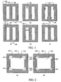
- FIGs.1(a)-(f) illustrate a mask 100 representing a simple integrated circuit design which contains some of the common mask defects that occur during the mask manufacturing process.
- the mask 100 comprises an opaque area 105, typically made of chrome, and clear areas 110 and 120 which represent the geometry primitives to be transferred onto the photoresist layer, and typically made of quartz.
- Fig. 1(a) illustrates an isolated pinhole defect 125 in the opaque area 105 of the mask 100.
- Fig. 1(b) illustrates an isolated opaque spot defect 130 in the clear area 110 of the mask 100.
- FIG. 1(c) illustrates edge intrusion defects 140 in the clear areas 110 and 120 of the mask 100.
- Fig. 1(d) illustrates edge protrusion defects 145 in the opaque area 105 of the mask 100.
- Fig. 1(e) illustrates a geometry break defect 150 in the clear area 110 of the mask 100.
- Fig. 1(f) illustrates a geometry bridge defect 155 in the opaque area 105 of the mask 100.
- Figs. 2(a)-(b) illustrate possible defects which may occur on a mask which utilizes optical proximity correction features.
- Fig. 2(a) illustrates a simple desired mask design 200 consisting of an opaque area 205, a clear area 210 which represents the shape desired to be transferred to the photoresist, and design serifs 215 which are added to the design to correct for optical proximity effects.
- Fig. 2(b) illustrates the mask 220 which could be produced by a typical electron beam machine given the mask design 200 as an input.
- the mask 220 comprises an opaque area 225, a clear area 230, and modified serifs 235. Note that the shape of the modified serifs 235 is different than the shape of the design serifs 215.
- the size of the serifs is very small -- they are designed to be smaller than the optical resolution of the lithography process to be used -- and the electron beam typically can not perfectly reproduce the design serif 215 shape onto the mask material.
- the result would be similar for masks which utilize other optical proximity correction features such as hammerheads, bias bars and assist bars.
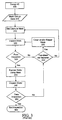
- Figs. 1 and 2 One typical method of inspecting a mask for defects such as those illustrated in Figs. 1 and 2 is illustrated in the flowchart of Fig. 3 .
- the mask design data is provided to a device such as an electron beam or laser writing machine and a mask is manufactured 315.
- the mask is then inspected for defects as shown at process block 320.
- the inspection may, for instance, be carried out by scanning the surface of the mask with a high resolution microscope (e.g., optical, scanning electron, focus ion beam, atomic force, and near-field optical microscopes) and capturing images of the mask. These mask images may then be observed by engineers off-line or mask fabrication workers online to identify defects on the physical mask.
- a high resolution microscope e.g., optical, scanning electron, focus ion beam, atomic force, and near-field optical microscopes
- the next step is determining whether or not the inspected mask is good enough for use in the lithography process. This step can be performed offline by a skilled inspection engineer, or by fabrication workers online possibly with the aid of inspection software. If there are no defects, or defects are discovered but determined to be within tolerances set by the manufacturer or end-user, then the mask is passed and used to expose a wafer as shown at process block 340. If defects are discovered that fall outside tolerances, then the mask fails the inspection 325, and a decision 330 must be made as to whether the mask may be cleaned and/or repaired to correct the defects 335, or whether the defects are so severe that a new mask must be manufactured 315. This process is continued until a manufactured mask passes the inspection 325.
- a physical mask is produced which passes the inspection, it is important to further inspect the mask to ensure that the mask will produce the desired image on a photoresist after a wafer is exposed to light through the mask. This is typically performed by undertaking the costly step of actually exposing and processing a wafer using the mask that is being inspected as shown at process block 340.
- the processed wafer is then inspected at block 345, and a decision 350 is made to determine whether there are any defects and whether the defects fall within tolerances. If discovered defects are substantial, then, as before, it is determined 330 whether the defects can be repaired 335 or whether a new mask must be produced 315. This process is continued until a mask is manufactured that will produce desired wafer patterns and that will pass the wafer level inspection shown at block 350. This mask is then used in the lithography process to expose the corresponding layer in the overall manufacturing process.
- a defect is "not printable” means that it has little effect on the expected outcome of a particular stepper exposure, even though it may become “printable” under a different set of stepper exposure conditions.
- printability is highly dependent on the stepper conditions, because a defect may print under one set of conditions, but not another. These conditions include: defect size, wavelength, numerical aperture, coherence factor, illumination mode, exposure time, exposure focus/defocus, and the reflection/transmission characteristics of the defect among others.
- inspection tools that are in use include tools which inspect masks both on-line (ie. within the production line) and off-line.
- Conventional on-line inspection tools typically scan the entire mask area looking for defect areas, and some may also compare the inspected result with the mask layout database when defects are detected.
- the defect analysis of the typical on-line inspection tools are based primarily (or solely) on the size of the defect picked up by the optics to define the severity of a particular defect. While this scheme has been somewhat successful in the past, today's masks are designed with smaller and smaller features, using advanced and unconventional methods such as OPC. Due to these changes, conventional methods of inspection are rapidly proving to be inadequate because they do not address several issues.
- a defect prints or not greatly depends on both its location and size, not just size or transmission/reflection characteristics alone. For example, a large defective spot in an isolated area may have little or no effect on the current and subsequent process layers. On the other hand, a small spot near a corner or an edge, or critical area should not be dismissed without closer examination. This is true for both conventional binary masks and advanced masks.
- advanced OPC mask features can trigger false defect detections. The typical conventional scheme can falsely report an OPC feature or an imperfect OPC feature (e.g., rounded serifs as illustrated in Fig. 2 ) as a defect, when it actually has little impact on the end result.
- OPC features are typically designed for a specific set of stepper parameters, but conventional tools' sliding scales are blind to these optical parameters.
- phase information is not properly incorporated into consideration, if at all, in the typical conventional defect inspection scheme. Therefore, phase shifting masks are not properly inspected. Finally, even though a defect may not appear to print, it might affect the process latitude in a way that will decrease yield and not be detected by conventional on-line defect inspection systems.
- off-line inspection stations which either scan for defects directly or review previously stored undeterminable defect data from an on-line tool, also face the same issues.
- these issues may require expensive engineers' time to be resolved, and thus diminish throughput while raising cost.
- an engineer's judgement magnitude of the defect printability/classification problem is greatly reduced due to experience and know-how, still, there is not enough certainty and accuracy until the defect is viewed as it appears on an actual wafer after exposure through the mask. This is especially true in today's lithography steppers using non-standard illumination models such as annular and quadruple.
- AIMS stepper equivalent Aerial Image Measurement System
- AIMS is focused on the printability of discrete locations identified beforehand that are imported in the form of a list of potential defect so that the mask can be moved swiftly from site to site to evaluate the printability of these defects.
- the measured aerial image is compared to a computer simulated image where the actual illumination parameters of the aerial image are used for the simulated image.
- the mask illumination source is set up to emulate a specific stepper equivalent condition.
- the important decision to be made is whether a given defect will "print" on the underlying photoresist in a lithography process under specified conditions. If a mask defect does not print or have other effects on the lithography process (such as unacceptably narrowing the photolithography process window), then the mask with the defect can still be used to provide acceptable lithography results. Therefore, one can avoid the expense in time and money of repairing and/or replacing masks whose defects do not print. What is desired then, is a method and apparatus for inspecting masks used in the photolithography process that solve the aforementioned problems of currently existing mask inspection systems.
- the present invention affords mask manufacturers and wafer fabricators a method and apparatus for mask inspection in which a simulation of the wafer image of a mask under inspection can be generated.
- the method is further characterized by the additional steps of providing a set of photoresist process parameters and generating a second simulated image in response to the set of photoresist process parameters.
- the second simulated image comprises a simulation of an image which would be printed on a wafer if the wafer were exposed to an illumination source directed through the portion of the mask, wherein the wafer comprises a coating of photoresist material characterized by the set of photoresist process parameters.
- the generation of the first simulated image can be calibrated to take into account a set of photoresist process parameters such that the first simulated image comprises a simulation of an image which would be printed on a wafer if the wafer were exposed to an illumination source directed through the portion of the mask, wherein the wafer comprises a coating of photoresist material characterized by the set of photoresist process parameters.
- the method is further characterized by the additional steps of providing a set of etching process parameters and generating a second simulated image in response to the set of etching parameters.
- the second simulated image comprises a simulation of an image which would be transferred on a wafer if the wafer were etched in accordance with the etching process parameters after the exposure to the illumination source.
- the generation of the first simulated image can be calibrated to take into account a set of etching process parameters such that the first simulated image comprises a simulation of an image which would be transferred on a wafer if the wafer were exposed to an illumination source directed through the portion of the mask and etched in accordance with the set of etching process parameters.
- the method is characterized by the additional steps of providing a reference description of the portion of the mask and providing a reference image.
- the reference image comprises a representation of an image that would be printed on a wafer if the wafer were exposed to an illumination source directed through a second mask, wherein the second mask is described by the reference description.
- the reference description comprises a physical mask which has been determined to be free from defects.
- the reference description comprises data in a format such as GDS-II, MEBES, CFLAT, digitized or discretized, and the reference image is a simulated image.
- the method includes comparing the first simulated image with the reference image. Comparing the first simulated image with the reference image may comprise generating a third simulated image which comprises the difference between the first simulated image and the reference image and/or generating a process window related output for each of the images and comparing these process window outputs.
- Generating the process window related outputs includes providing a set of wafer image acceptance criteria, and generating a range of values for at least one optical parameter in the set of optical lithography parameters, for which the images fall either inside or outside the set of wafer image acceptance criteria.
- the method is further characterized by the additional step of analyzing the first simulated image for defects on the first mask.
- the analyzing step may include the generation of a process window related output, the generation of an analysis output wherein the analysis output comprises a signal which indicates whether the first mask either passed or failed the inspection, and/or the generation of a performance output wherein the performance output comprises data indicating the mask's effect on the performance of an integrated circuit if the mask were to be used in the production of the integrated circuit.
- the method steps of the above embodiments may in one instance be performed by a computer running a program which implements these steps wherein the program is stored on any appropriate computer storage media such as a hard disk drive or server.
- an inspection tool is used to locate an area on the mask which contains a potential defect.
- the inspection tool then generates the defect area image and provides the defect area image to the simulator apparatus.
- the inspection tool includes a high resolution optical microscope and a CCD camera.
- the defect area images may be either stored for later inspection, or provided on the fly for immediate analysis.
- the present invention may be alternatively characterized as an apparatus for inspecting a mask used in optical lithography in accordance with claim 36.
- the apparatus also includes a resource for receiving a set of photoresist process parameters.
- the image simulator generates a second simulated image in response to these photoresist parameters.
- the second simulated image comprises a simulation of an image which would be printed on a wafer if the wafer were exposed to an illumination source directed through the portion of the mask, wherein the wafer comprises a coating of photoresist material characterized by the set of photoresist process parameters.
- the apparatus includes a resource for receiving a set of etching process parameters.
- the image simulator generates a second simulated image in response to these etching parameters.
- the second simulated image comprises a simulation of an image which would be transferred on the wafer if the wafer were etched in accordance with the etching process parameters after the exposure to the illumination source.
- the apparatus includes a resource for receiving a reference description of the portion of the mask and a resource for providing a reference image.
- the reference image comprises a representation of an image that would be printed on a wafer if the wafer were exposed to an illumination source directed through a second mask, wherein the second mask is described by the reference description.
- the reference description comprises a physical mask which has been determined to be free from defects.
- the reference description comprises data in a format such as GDS-II, MEBES, CFLAT, digitized or discretized, and the reference image is generated by the image simulator.
- the apparatus includes an image comparator which compares the first simulated image with the reference image.
- the image comparator generates a third simulated image which comprises the difference between the first simulated image and the reference image.
- the image comparator generates first and second process window related outputs. Generating the process window related outputs, in one embodiment, includes providing a set of wafer image acceptance criteria to the image comparator. The image comparator then generates a range of values for at least one optical parameter in the set of optical lithography parameters for which the images fall either inside or outside the set of wafer image acceptance criteria.
- the apparatus includes a defect analyzer which analyzes the first simulated image for defects on the mask.
- the defect analyzer may generate a process window related output, an analysis output comprising a signal which indicates whether the mask either passed or failed the inspection, and/or a performance output wherein the performance output comprises data indicating the mask's effect on the performance of an integrated circuit if the mask were to be used in the production of the integrated circuit.
- the apparatus may include an inspection tool that is used to locate an area on the mask which contains a potential defect.
- the inspection tool may also generate the defect area image and provide the defect area image to the simulator apparatus.
- the inspection tool comprises a high resolution optical microscope and a CCD camera.
- the illumination source may comprise either a visible or non-visible (such as Deep Ultraviolet or DUV) illumination source.
- the set of optical lithography parameters may comprise data representing the numerical aperture, wavelength, sigma, lens aberration and defocus of an optical lithography system, and the critical dimensions of the mask among other parameters.
- the design of the first mask may comprise a bright field, dark field, or phase shifting mask design.
- Photolithography is a process whose input is a mask and whose output is the printed patterns on a wafer.
- the printed result from a mask is what design engineers, lithographers, and mask manufacturers really care about.
- the only way to inspect this printed result was to perform an actual wafer exposure and therefore incur potentially unnecessary costs in time and money.
- the present invention solves some of the problems of these prior methods by providing for mask inspection that takes printability into account without the need for the expensive steps of actually exposing a wafer.
- the present invention is capable of using a captured image of a mask -- that accurately enough represents the physical mask (i.e.
- the present invention can be used to simulate the wafer exposure based on captured images of the mask areas surrounding the potential defects. In this way, the printability of potential defects can be directly analyzed without taking the expense of an actual wafer exposure.
- the simulation can be controlled to take into account any number of parameters associated with the photolithography process, thereby making the printability determination process specific. Still further, the simulation of each defect can be performed at numerous values of certain process variables that might vary during actual exposure (such as defocus) in order to determine the effect the potential defects have on the wafer manufacturing process window. Subsequent processing can also be modeled with accuracy and with little loss of speed by calibrating the process to take into account photoresist process and etching process parameters.
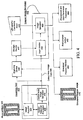
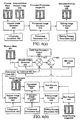
- Fig. 4 illustrates, in simplified process flow diagram form, a process of inspecting a mask for defects in accordance with one embodiment of the present invention.
- the process utilizes an inspection tool 400 and a stepper image generator 410.
- the inspection tool 400 may comprise an image acquiror 430, a defect detection processor 440, and a defect area image generator 442.
- the inspection tool 400 may be all inclusive in that it contains each of the aforementioned elements in one package. This all-inclusive tool 400 setup is typically used in on-line mask inspection.
- the tool 410 may comprise a number of separately existing elements which interface with each other as is typically used in off-line mask inspection.
- the image acquiror 410 is a separate device from the defect detection processor 440.
- the image acquiror 430 may comprise a high resolution imaging device such as a high resolution optical microscope, a scanning electron microscope (SEM), a focus ion beam, an atomic force microscope, and a near-field optical microscope such as is well known in the art of mask inspection.
- the image acquiror 430 scans all or a portion of the mask 420.
- the image acquiror may also comprise a device such as a CCD camera capable of interfacing with the particular type of microscope used and digitizing the image information from the microscope. For instance, a CCD camera that creates n-bit gray scale image data that is representative of the image from the microscope may be used.
- the image data may be stored in a format such as Windows BMP on any type of appropriate media including a computer hard disk drive, a CDROM, and a server.
- the defect detection processor 440 controls the image acquiror 410.
- the defect detection processor 440 provides control signals which control the manner in which the image acquiror 410 scans the mask. Further, the defect detection processor 440 compares the mask images provided by the image acquiror 410 to a set of potential defect criteria and determines what areas of the mask contain potential defects.
- the defect detection processor 440 comprises a computer running a program of instructions and interfacing with the image acquiror 430 such that the scanning of the mask is done in the desired manner. In one embodiment, the program operates such that a user may change the parameters of the scanning performed on the mask 420.
- the image acquiror 410 could be replaced with a preexisting image of a mask or a portion of a mask.
- any representation of the physical mask 420 that is capable of being analyzed by the defect detection processor 440 is acceptable as an input.
- the defect detection processor 440 also controls the defect area image generator 442 which provides images of those areas of the mask 420 which may contain defects. For instance, as the image acquiror 430 provides image input scanned from the mask 420 to the defect detection processor 440, the defect processor 440 determines whether that portion of the mask scanned contains any potential defect areas based on predetermined defect criteria. These criteria may, in one embodiment, be changed by a system user. If a potential defect is discovered, the defect processor 440 signals the defect area image generator to provide a defect area image of the area surrounding the potential defect. The defect area image generator 442 thus provides defect area image data 444.
- the defect area image generator 442 may be a part of the image acquiror 430, for instance, the defect area image generator 442 may comprise the CCD camera of the image acquiror 430. In another embodiment, the defect area image generator 442 may be a separate device which receives image input from the image acquiror 430.
- the embodiments of the inspection tool 400 may be utilized to provide data for the stepper image generator 410 in a number of ways.
- the image acquiror 430 could scan the entire mask 420 or a portion of the mask 420 without any control from the defect detection processor 440 and store the resulting image data in a storage device 447 such as a server after digitizing the data with a digitizing device 446 such as an image grabber.
- a storage device 447 such as a server after digitizing the data with a digitizing device 446 such as an image grabber.
- This same image data could also be provided directly to the stepper image generator 410 via a real time data feed.
- the defect area image generator 442 may provide the defect area image data 444 either directly to the image generator 410 via a real time data feed (on-line inspection) or provide the image data 444 to the digitizing device 446 and then to the storage device 447 for later off-line inspection.
- the stepper image generator 410 comprises an input device 450 and an image simulator 460.
- the input device 450 in the case of stored image data from the storage device 447, may comprise any hardware suitable for reading the type of media upon which the image data is stored, including a computer hard disk drive, a CDROM reader, and a personal computer attached to a server via a network, among others.
- the input device may comprise a digitizing device such as an image grabber.
- the input device may comprise an 8-bit frame grabber device such as those that are known in the art including the MatroxTM MeteorTM and PulsarTM.
- the input device 450 also receives other input data such as lithography conditions input 445.
- the image simulator 460 comprises a computer implemented program which accepts the stored image data or real time feed from the input device 450, and produces a simulation of the stepper image 470 on a wafer for the physical mask 420.
- the image simulator 460 program may be run on a variety of computer platforms including: a PC using the Windows 95TM or NTTM 4.0 operating system with 128 MB of RAM and a 200 MHz Pentium ProTM microprocessor, either stand alone or connected to a network, and a SUNTM workstation computer among others.
- the amount of time required for one embodiment of the image simulator 460 to simulate an image of conventional CCD array size is less than a second.
- the inspection tool 400 and stepper image generator 410 operate to produce a simulated stepper image 470, a simulated process window 480 output for a physical mask 420, and/or other performance related output used to characterize, define, or measure the effect of a defect(s) on integrated circuit performance as follows.
- the physical mask 420 is first inspected by the inspection tool 400.
- the inspection tool 400 scans the physical mask 420 for possible defects and the defect area image generator 442, pursuant to direction from the defect detection processor 440, generates defect area images 432 of those areas of the mask containing possible defects.
- the defect area image data 444 is then either fed to the input device 450 in real time, and/or stored in the storage device 447 via the digitizing device 446 for later inspection.
- the input device 450 receives the defect area image data 444 from the defect area image generator 442 or the storage device 447.
- the defect area image data 444 is then output to the image simulator 460.
- the image simulator 460 receives lithography conditions input 445.
- the lithography conditions input 445 contains data that is specific to the lithography conditions and system parameters under which the physical mask is to be later exposed if it passes inspection. This data may include parameters such as the numerical aperture of the system (NA), the coherency value of the system ( ⁇ ), the wavelength of the illumination being used in the system ( ⁇ ), the defocus of the exposure, lens aberrations, substrate conditions and the critical dimensions of the design among others.
- the lithography conditions input 445 may contain a range of these parameters such that the simulation can be performed a number of times for different combinations of these parameters. In this manner, the printability of a mask defect can be analyzed over a range of possible lithography conditions, and the effect of a potential mask defect on the process window can also be analyzed.
- the image simulator 460 receives the defect area image data 444 from the input device 450 and the lithography conditions input 445, and generates a simulated stepper image 470 which is a simulation of the wafer exposure which the defect area of the physical mask 420 would generate if an optical lithography exposure had been performed under the same conditions as the lithography conditions input 445.
- the image simulator 460 can generate a simulated process window 480 which represents the effect the potential defect area has on the process window, and/or a performance output 482 as discussed above.
- the image simulator 460 is able to generate a simulated stepper image 470 for a potential defect area of a mask of a number of different types of mask design including bright field, dark field, and attenuated phase-shifting mask designs.
- the simulated stepper image 470, the simulated process window 480, and/or the performance output 482 may then be inspected to determine the printability of any identified potential defect area without actually taking the expense of exposing a real wafer with the mask, as will be explained in more detail with respect to Figs. 8-11 .
- the image simulator 460 could take into account the parameters associated with the photoresist material to be used and/or the etching process to be used on the exposed wafer in order to simulate the end result of these processes as shown by block 484 and discussed more fully below with respect to Fig. 6 .
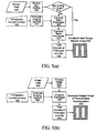
- Figs. 5(a)-(b) illustrate in process flow diagram form, two embodiments of the image simulation process utilized in the present invention to produce simulated stepper images of an exposed wafer.
- Fig. 5(a) illustrates an embodiment of the process as it would be used on a design mask such as by the design image simulator 960 to be described below with respect to Fig. 9 .
- Fig. 5(b) illustrates an embodiment of the process as it would be used on a captured image of a physical mask such as by the image simulator 460 of Fig. 4 , the image simulators 830 and 860 of Fig. 8 , and the mask image simulator 950 and design image simulator 960 of Fig. 9 .
- Figs.5(a)-(b) Prior to discussing the specifics of Figs.5(a)-(b) however, it would be beneficial to lay some of the background behind the simulation processes illustrated therein.
- the above nonlinear integral equation is far too complex to be applied efficiently to realistic integrated circuit patterns.
- the image simulations to be discussed with respect to Figs. 5(a)-(b) are, in one embodiment, produced using a process that is a simplified approximation of the Hopkins model as applied specifically to integrated circuits.
- the Hopkins model is first effectively broken down into a number of low pass filters that are applied to the input data. The resulting images are then added to generate the simulated image.
- OCA Optimal Coherent Approximation's
- OCD Optimal Coherent Decompositions
- the computation required to compute the image reduces to O (N log 2 N) using the Fast Fourier transform (FFT), where N is the number of discrete sample points considered.
- FFT Fast Fourier transform
- This exploitation of the integrated circuit structure is generally accomplished by: 1) defining a small set of basis functions that can be used to represent integrated circuit patterns, 2) computing the preimages of the defined basis functions using the imaging kernels, 3) using the preimages of the basis functions as a set of building blocks to construct the preimages of the mask pattern, and 4) combining the preimages to obtain the image of the mask pattern.
- a data file containing the design data 500 of the mask is provided as an input, and the set of box widths existing in the design is extracted from the design data at block 505.
- the lithography conditions for the simulation are provided as an input at block 502, from which the imaging kernels ⁇ k are computed at block 515 as described above.
- a determination is then made if basis preimages for all of the extracted box widths have been precalculated and exist in a database library at block 510.
- Basis preimages are then computed at block 520 for those widths whose basis preimages have not been precalculated.
- the simulation process using OCA as described above is described below with respect to Fig. 5(b) as it would be used on a captured image of a physical mask such as by the image simulator 460 of Fig. 4 and the mask image simulator 950 of Fig. 9 .
- the embodiment of the process described below is substantially different than the one described above with respect to Fig. 5(a) because of the form of the input data file.
- the input image data 550 which comprises digitized image data that in one embodiment is an 8-bit gray scale image file in a format such as Windows BMP, is first provided to block 555. This data is then processed at block 555 in order to increase the sensitivity of the overall process and to produce a data file whose image is closer to what a mask actually looks like.
- the processing at block 555 may comprise a multiple thresholding process in which the 256 possible intensity levels of the 8-bit file are folded into 4 or 6 levels.
- the processing at block 555 could comprise a type of non-linear filtering to increase the process sensitivity such as taking the logarithm of the image intensity which would enhance the lower intensities.
- the lithography conditions for the simulation are provided as an input at block 552, from which the imaging kernels ⁇ k are computed at block 560 as described previously.
- the preimages of the wafer image are computed at block 565, and at block 570 the intensity of each preimage is taken and added together to form the simulated stepper image of the physical mask representation 575 in accordance with equation 4.
- the mask function f is defined entirely by pixel data, there is no spatial structure which can be taken advantage of as with a design mask.
- the step of block 525 of Fig. 5(a) can be avoided since there is only one basis preimage to be calculated for each of the imaging kernels ⁇ k .
- the computation of preimages at block 565 also differs from its corresponding block 520 of Fig. 5(a) . For, there is no preexisting knowledge from which one could limit the convolution to only a small number of sample points and still get an accurate approximation of the preimage.
- the image simulation process of the present invention may, in alternate embodiments, take into account the parameters associated with the photoresist material to be used and/or the etching process to be used on the exposed wafer in order to simulate the end result of these processes.
- Figs. 6(a)-(b) illustrate, in simplified process flow diagram form, two alternate embodiments of the invention which take these parameters into account.
- Fig. 6(a) illustrates the use of additional simulation models in conjunction with the lithography simulation discussed above to produce images which take photoresist and/or etching parameters into account.
- a physical mask 604 to be simulated is provided as an input along with lithography conditions 602 to the stepper image generator 600 which produces a simulated mask stepper image 606 in the manner discussed above with respect to Figs. 4 and 5 .
- Data representing the simulated mask stepper image 606 - which may be in the form of image intensity data - is then provided along with photoresist parameters 612 to a photoresist image simulator 610 which in turn produces a simulated photoresist image 616.
- the simulated photoresist image 616 represents an image of a wafer exposed through the physical mask 604 wherein the wafer was coated with a photoresist material described by the photoresist parameters 612.
- Data representing the simulated photoresist image 616 may then be provided along with etching process parameters 622 to an etching image simulator 620 which in turn produces a simulated etching image 626.
- the simulated etching image 626 represents an image transferred on a wafer after the wafer was exposed through the physical mask 604 wherein the wafer was coated with a photoresist material described by the photoresist parameters 612 and then etched in accordance with the etching process parameters 622.
- these photoresist parameters 612 and etching process parameters 622 are able to be changed by a user to match those which will be used in the actual production of a wafer.
- the photoresist parameters 612 may include thickness, contrast, pre-bake time, post-bake time, development time, photoresist concentration, developer solution concentration, and light absorption of the photoresist among others.
- the etching process parameters 622 may include etching time, etching method, and concentration among others.
- the photoresist image simulator 610 comprises a computer implemented program which accepts image data provided by the stepper image generator 600 and produces the simulated photoresist image 616. As before with respect to Fig.
- the image data may be provided in real time or from a storage device which has previously stored the simulated mask stepper image data 606.
- the etching image simulator 620 comprises a computer implemented program which accepts image data -- either in real time or previously stored -- provided by the photoresist image simulator 610 and produces the simulated etching image 626.
- the photoresist image simulator 610 and the etching image simulator 620 programs may be run on a variety of computer platforms including: a PC using the Windows 95TM or NTTM 4.0 operating system with 128 MB of RAM and a 200 MHz Pentium ProTM microprocessor, either stand alone or connected to a network, and a SUNTM workstation computer among others.
- the photoresist image simulator 610 program described above may in one embodiment utilize the photoresist model developed by T.A. Brunner and R.A. Ferguson of IBM as set out in "Approximate Models for Resist Processing Effects", SPIE, Vol. 2726, p. 198 , which is incorporated herein by reference as if set forth fully.
- the etching image simulator 620 program described above may in one embodiment utilize the model developed by TMA as set out in " Accurate Modeling of Deep Submicron Interconnect Technology", TMATIMES, Vol. IX, No. 3, (Fall 1997 ) which is incorporated herein by reference as if set forth fully.
- Fig. 6(b) illustrates an alternate embodiment in which photoresist or etching parameters can be accounted for in the simulation by calibrating the lithography image simulation discussed previously with respect to Figs. 4 and 5 .
- the process illustrated in Fig 6(b) comprises calibrating the stepper image generator 600 with the calibrator 660 such that a desired real result 650for instance, a photoresist image or etching image -- is obtained when a physical mask is provided as an input to the system.
- the process comprises first initializing the system by providing a reference data 655 to the stepper image generator 600 and the calibrator 660.
- the reference data 655 may comprise any data which is representative of a known mask such as the design layout data for the mask to be simulated, or an image of a similar mask which has been determined to be free from defects.
- the stepper image generator 600 provides an image simulation output to a summing device 675 where it is added to the output of the calibrator 660.
- the output of the summing device 675 is provided to a difference device 680 along with a real result 650.
- the desired real result 650 which is provided to the difference device 680 may, in one embodiment, comprise either an etch result 640 or a photoresist result 630, which in one embodiment is chosen by the user.
- the photoresist result may comprise either an actual photoresist image 636 or a simulated photoresist image from a photoresist image simulator 610 which again, may be chosen by the user in one embodiment.
- the actual photoresist image 636 could be an actual image of a wafer which has been exposed under the photoresist conditions the user wishes to simulate.
- the photoresist image simulator 610 generates a simulation of the image on a photoresist coated wafer which has been exposed through a mask.
- the reference data 665 is provided to an uncalibrated stepper image generator 600 which provides its output to the input of the photoresist image simulator 610 which generates a photoresist simulation as discussed above -- in this manner a proper comparison can be performed between the real results 650 data and the summing device 675 output.
- the etch results may comprise either an actual etching image 646 or a simulated etching image from an etching image simulator 620 at the choice of the user.
- the actual photoresist image 646 could be an actual image of a wafer which has been exposed under the photoresist conditions the user wishes to simulate, and then etched in accordance with the etching parameters desired to be simulated.
- the etching image simulator 620 generates a simulation of the image transferred on a photoresist coated wafer which has been exposed through a mask and then etched.
- the initial input to the etching simulation is the reference data 655 -- in this manner a proper comparison can be performed between the real results data and the summing device 675 output.
- the difference device 680 takes the difference between the real result 650 and the output of the summing device 675, and the output of the difference device 680 is provided to the minimizer 670.
- the minimizer 670 acts to zero the output of the difference device 680 by adjusting the output of the summing device 675.
- the minimizer 670 performs this by generating feedback signals to the stepper image generator 600 and the calibrator 660 such that the values assigned to particular physical and non-physical variables respectively are altered in a predetermined manner to zero the output of the difference device 680.
- simulation of a physical mask 604 then comprises simply providing image data of defect areas to the stepper image generator 600 and calibrator 660 as discussed earlier with respect to Fig. 4 , and then summing the output of these two devices.
- the end result is the calibrated simulation output 690 which reflects the desired simulation result such as a photoresist or etching processes.
- the calibrator 660 may comprise, in one embodiment, a computer program which provides an output comprising a set of non-physical variables whose values are dependent upon the reference data 655 input and the feedback from the minimizer 670.
- the summing device 675, difference device 680 and minimizer 670 may also, in one embodiment, comprise a computer program which executes the steps set out above.
- Figs. 7(a)-(b) illustrate, in block diagram form, various situations in which the present invention could be used in the areas of photolithography mask manufacture and wafer fabrication.
- a mask manufacturer uses design data 700 supplied by an integrated circuit designer to produce a physical mask 705 which must be inspected prior to being sent to a wafer fabrication plant 730. If the mask fails inspection, it must be either repaired 720 or reprinted 725 and then reinspected. This inspection could be done on-line 710 or off-line 715 using various embodiments of the present invention.
- an on-line 710 embodiment of the present invention could be configured to work in parallel with a conventional mask inspection tool where the inspection is on-the-fly.
- All such an embodiment would need is a feed of image data representative of any potential defects the mask inspection tool detects in order to produce wafer simulations of the current microscope image.
- Another embodiment of the present invention could be implemented directly within an on-line inspection system, to provide quick real time assessment of potential defect areas flagged by a SEM for instance.
- off-line inspection 715 one embodiment of the invention can utilize previously stored defect data independently of, or together with, an off-line microscope review station.
- an embodiment of the present invention could be utilized by mask manufacturers to inspect the repair site of a mask undergoing repair 720 in an in situ manner to qualify individual repair sites separately on the mask.
- a wafer fabricator receives a physical mask from a manufacturer, and quality checks 750 the mask to ensure that it meets the required specifications prior to being used in lithography 760 to produce wafers 770.
- This quality checking 750 step can be enhanced by inspecting the mask 755 with an embodiment of the invention similar to those discussed above with respect to Fig. 7(a) .
- a wafer fabricator can use an embodiment of the present invention to periodically requalify 765 a mask that has been used for a number of exposures. This becomes necessary because masks can be damaged or contaminated with particles after repeated use.
- an embodiment of the invention can be used to assist in overseeing this quality control process to decide whether the mask needs to be cleaned or remade.
- Fig. 8 illustrates, in a process flow diagram, one embodiment of a system for both on-line and off-line inspection of a photolithography mask in accordance with one embodiment of the invention.
- the system includes an inspection tool 805, an on-line inspection station 820, and an off-line inspection station 850.
- the inspection tool 805 includes an image acquiror 810, a defect detection processor 815 and a defect area image generator 817 each of which may operate as discussed above with respect to Fig. 4 .
- the on-line inspection station 820 includes an input device 825 such as discussed previously with respect to Fig. 4 , an image simulator 830 such as described previously with respect to Figs. 4 and 5(b) , and a defect analyzer 835.
- the off-line inspection station 850 includes an image simulator 860 such as described previously with respect to Figs. 4 and 5(b) , and a defect analyzer 870.
- the system of Fig. 8 operates to provide a number of possible outputs with respect to the inspection of a mask as follows.
- the physical mask 800 is first inspected by the inspection tool 805.
- the inspection tool 805 scans the physical mask 800 for possible defects and the defect area image generator 817 generates defect area images of those areas of the mask containing possible defects.
- the defect area image data is then analyzed by either the off-line inspection station 850, the on-line inspection station 820, or both.
- the defect area image data is provided to a digitizer device 853 as previously discussed, and then stored in storage device 855 in any suitable image data format, such as Windows BMP, and on any suitable storage media as discussed previously.
- the defect area image data is then input to the image simulator 860 along with lithography conditions input 862, and a simulation of the stepper image on a wafer for the mask defect area is produced.
- the lithography conditions input 862 contains process specific data as discussed previously with respect to Fig. 4 . In one embodiment this simulation is performed as discussed with respect to Fig. 5(b) .
- the simulation of the stepper image is then provided to the defect analyzer 870 so that the potential defect can be analyzed for printability and process window effects.
- the defect analyzer 870 may comprise a device which allows viewing the image of the simulation by an operator such as a lithography engineer who can then make judgements as to the severity of the potential defect.
- the defect analyzer 870 may also comprise a device which allows comparison of the simulated image of the defect area with a simulation of an area on the design layout which corresponds to the defect area as will be discussed with respect to Fig.9 .
- a decision 875 is made as to whether or not the mask passed the inspection. If the mask passes the inspection it is then used in the lithography process 880, while if the mask fails the inspection it is either remade or the defect(s) is/are repaired 885.
- the defect area image data may be provided in real time to the input device 825, which in turn outputs this data to the image simulator 830.
- the image simulator 830 also receives lithography conditions input 832 which contains process specific data as discussed previously with respect to Fig. 4 .
- the image simulator 830 generates a simulation of the stepper image on a wafer for the mask defect area, which, in one embodiment is generated in accordance with the process discussed with respect to Fig. 5(b) .
- the image simulator 830 can generate a number of simulations for the defect area using ranges of input lithography conditions, and then generate a simulated process window which represents the effect the potential defect area has on the process window.
- the output of the image simulator 830 is provided to the defect analyzer 835 which analyzes the defect area simulation and/or the simulated process window and provides an analysis output 840.
- the defect analyzer 835 is a computer implemented program which processes the simulation data in light of user input defect criteria to determine whether the defect is severe enough to warrant further inspection, or whether the defect area does not print or otherwise effect the process window over a user defined set of possible lithography conditions.
- the analysis output 840 comprises one of a number of different decision indicators.
- these indicators may include “reject”, “repair”, “accept”, and “undecided” based upon a number of different criteria that the user may input into the defect analyzer 835.
- the analysis output is "accept”
- the mask is sent on to the lithography process 880 without further inspection.
- the analysis output is "reject”, “repair”, or “undecided”
- the defect area image data may be stored at block 845 and then input to the off-line inspection station 850 for further analysis by a more skilled operator such as a lithography engineer.
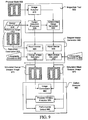
- Fig. 9 illustrates, in a process flow diagram, another embodiment of a system for inspection of a photolithography mask in accordance with one embodiment of the present invention.
- the system includes an inspection tool 900, a stepper image generator 940, and a defect analyzer 990.
- Inputs to the system include a physical mask 905, a reference description 935, and lithography conditions 965.
- the reference description 935 comprises data which represents a defect free design layout of the physical mask 905.
- this data may comprise reference image 912 which could be an image of a physical mask which has been previously inspected and determined to be free from defects.
- this reference description may comprise the design layout data 910 for the physical mask 905.
- the inspection tool 900 includes an image acquiror 915, a defect detection processor 925 and a defect area image generator 930 each of which may operate as discussed above with respect to Fig. 4 .
- the stepper image generator 940 includes input devices 945 and 955 such as discussed previously with respect to Fig. 4 , a mask image simulator 950 such as described previously with respect to Figs. 4 and 5(b) , and a design image simulator 960 which operates as discussed with respect to Fig. 5(a) and/or Fig. 5(b) depending on the input to the input device 955.
- the defect analyzer 990 may include an image comparator 980, a process window analyzer 985, and a performance output device 995.
- the system of Fig. 9 operates to inspect a physical mask 905 as follows.
- the physical mask 905 is first inspected by the inspection tool 900.
- the inspection tool 900 scans the physical mask 905 for possible defects and the defect area image generator 930 generates defect area images of those areas of the mask containing possible defects.
- the defect detection processor 925 may also receive design layout data 910 as an input. In this instance, for each defect area image that is generated, the defect detection processor 925 may operate to locate the corresponding area on the design layout data 910 and provide this information to input device 955.
- the design layout data 910 is in GDS-II format.
- the defect area image generator 930 provides the defect area image data to the input device 945 of the stepper image generator 940 which processes the data as discussed previously.
- the mask image simulator 950 receives the processed image data from the input device 945 and lithography conditions input 965, and generates a simulated mask stepper image 970 and simulated process window information in a manner described above with respect to Fig. 5(b) .
- the input device 955 of the stepper image generator 940 receives the design layout data 910 corresponding to the defect area from the defect detection processor 925 and provides the design image simulator 960 with design data representing an area to be simulated that corresponds to the defect area being simulated.
- the design image simulator 960 using the same lithography conditions input 965, generates a simulated design stepper image 975 and simulated process window information in a manner described above with respect to Fig. 5(a) .
- the reference image 912 may be provided to the input device 955, and the design image simulator 960 may then use the reference image data to generate the simulated design stepper image 975 and simulated process window information in a manner described above with respect to Fig. 5(b) .
- the simulated mask stepper image 970 and the simulated design stepper image 975 are provided to the image comparator 980 of the defect analyzer 990.
- the defect analyzer 990 includes a computer implemented program that is capable of displaying the images 970 and 975, and displaying the differences between the two such that an operator can visually detect any differences -- the output of an embodiment of such a program is illustrated in Figs. 17 and 20 below.
- the simulated process window data from the stepper image generator 940 is provided to the process window analyzer 985 of the defect analyzer 990.
- the process window analyzer 985 in one embodiment is a computer implemented program capable of displaying the effect that a potential defect area has on the overall process window of the lithography process as compared to the "perfect" design mask.
- the outputs of the stepper image generator 940 for the physical mask 905 and the reference description 935 are also provided to a performance output device 995.
- the performance output device 995 in one embodiment is a computer implemented program capable of determining and displaying the effect that one or more defects have on the overall performance of the integrated circuit for which the physical mask 905 will be used to produce.
- Figs. 10(a)-(c) illustrate an example of how a potential defect area could affect the overall process window of the photolithography process.
- Fig. 10(a) is an illustration of an x-y coordinate plot of data with exposure deviation % on the x-axis and lithography defocus (in nanometers) on the y-axis.
- Data curves 1002 and 1004 represent a typical plot of data for a first chosen area on a mask in which the area has no defect.
- the area between the curves 1002 and 1004 represents the range of defocus and exposure deviation values which would still give acceptable lithography results at the first chosen area in accordance with a user defined set of acceptance criteria.
- Data curves 1006 and 1008 represent a typical plot of data for a second chosen area on a mask in which the area has no defect.
- the area between the curves 1006 and 1008 represents the range of defocus and exposure deviation values which would still give acceptable lithography results at the second chosen area in accordance with the same user defined set of acceptance criteria.
- Area 1010 defines the overlap of the above two bounded areas, and represents the range of defocus and exposure deviation values which would give acceptable lithography results at both areas in accordance with the user defined set of acceptance criteria.
- the process window plot depicted in Fig. 10(a) could contain additional curves representing additional chosen areas on the mask in order to define the range of acceptable lithography conditions more finely. Further, different parameters could be plotted on the x-axis and the y-axis including critical dimension, temperature and exposure dose in order to determine the sensitivity of the acceptable lithography conditions to variations in the parameters affecting the lithography process.
- Fig. 10(b) is an illustration of a process window for the same mask as in Fig. 10(a) , except that the first chosen area contains a defect.
- data curves 1012 and 1014 represent a typical plot of data for a first chosen area on a mask in which the area has a defect.
- the area between the curves 1012 and 1014 represents the range of defocus and exposure deviation values which would still give acceptable lithography results at the first chosen area in accordance with a user defined set of acceptance criteria.
- Data curves 1016 and 1018 correspond directly with curves 1006 and 1008 of Fig. 10(a) , as does the area between curves 1016 and 1018.
- Area 1020 defines the overlap of the above two bounded areas, and represents the range of defocus and exposure deviation values which would give acceptable lithography results at both areas in accordance with the user defined set of acceptance criteria. Note that the defect at the first chosen area, in this example, has decreased the range of lithography conditions which will give an acceptable result. Note also that this could be the case, in some examples, even if the defect did not print.
- Fig. 10(c) is provided to clearly illustrate the effect that a defect at a mask area can have on the process window.
- Area 1030 represents the difference between area 1010 and area 1020, and therefore represents the range of lithography conditions that are effectively made unavailable to the lithographer as a result of the defect.
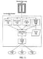
- Fig. 11 illustrates a process flow chart representing one embodiment of the on-line defect analyzer 835 of Fig. 8 .
- a simulated mask image 1100 such as provided by the image simulator 830 of Fig. 8 , is provided to the on-line defect analyzer 1110.
- the defect analyzer 1110 provides an indicator 1150 to a user, such as a mask fabrication line worker, as to the status of any defect area on the mask image 1100.
- This indication in one embodiment, comprises one of the three indicators "accept”, “reject”, or “repair”, and may be implemented with any means that alerts the user as to the status of the mask.
- the defect analyzer 1110 generates the indicator based upon an analysis of the mask image 1100 with respect to user input inspection criteria. In one embodiment, the defect analyzer 1110 assigns a defect severity score 1140 to the defect on the simulated mask image, and provides one of the three indicators in response to the defect severity score 1140.
- This defect severity score 1140 may be a weighted score which takes into account various parameters associated with the defect including, defect size and type 1120, defect context and location (i.e.
- each of the aforementioned inputs to the severity score 1140 may be weighted according to user preference.
- the defect analyzer 1110 is, in one embodiment, a program implemented by a computer which interfaces with a set of indicator lights to provide the output indicator 1150. As discussed previously with respect to Fig. 8 , the defect analyzer may also provide for the storage of defect data such that it may be later analyzed by an inspection engineer off-line.
- the remaining figures illustrate sample screen shots taken of a computer implemented program which utilizes one embodiment of the present invention. All images described as microscope images in the remaining figures were taken with a transmission mode microscope. Thus, bright areas represent quartz (clear) areas on the mask, and dark areas represent chrome (opaque) areas. The images described as simulated wafer images in the remaining figures are similarly represented in that bright areas represent areas on the photoresist that will be exposed to light, and dark areas represent areas on the photoresist that have not been exposed to light.
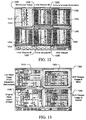
- Fig. 12 illustrates a screen shot 1200 comprising windows 1210, 1220, 1230, 1240, 1250, and 1260 in which a defective mask is simulated to print under 5 different stepper conditions.
- Window 1210 illustrates a captured microscope image of a mask containing various defects of different sizes such as defect 1212.
- Window 1220 illustrates the simulated wafer exposure of the mask of window 1210 under a particular set of I-line stepper conditions.
- Window 1230 illustrates the simulated wafer exposure of the mask of window 1210 under a set of I-line stepper conditions in which annular illumination is used.
- Window 1240 illustrates the simulated wafer exposure of the mask of window 1210 under a another particular set of I-line stepper conditions.
- Window 1250 illustrates the simulated wafer exposure of the mask of window 1210 under still another set of I-line stepper conditions.
- window 1260 illustrates the simulated wafer exposure of the mask of window 1210 under a particular set of Deep Ultra-Violet (DUV) stepper conditions.
- DUV Deep Ultra-Violet
- Fig. 12 illustrates the problem of identifying defect printability that is associated with the prior art. Note how all of the defects present in window 1210 do not show up or "print" in the final simulated wafer exposure under the various stepper conditions illustrated in windows 1220-1260. In particular, it is of note that defect 1212 does not print under some conditions as shown by defect simulation marks 1232 and 1242, while under other conditions defect 1212 does print as shown by defect simulation marks 1222, 1252, and 1262. Without the information provided in Fig. 12 , an inspection engineer would have to rely on his experience, or use actual wafer exposures to determine whether a defect will print (or otherwise detrimentally affect the process window as will be explained below) under a particular set of lithography conditions.
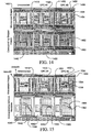
- Fig. 13 illustrates a screenshot 1300 of one embodiment of the graphical user interface of a computer implemented program utilizing one embodiment of the present invention.
- the screenshot 1300 comprises windows 1310, 1320, 1330, and 1340.
- Window 1310 illustrates a captured microscope image of a portion of a mask while window 1320 illustrates the simulated wafer exposure of the mask of window 1310 under a particular set of DUV stepper conditions.
- Window 1330 illustrates the original mask layout design of the portion of the mask shown in window 1310, and window 1340 illustrates the simulated wafer exposure of the original mask layout design of window 1330 using the same stepper conditions as for the simulation displayed in window 1320.
- the present invention allows one to compare directly the stepper image of the original design with the stepper image of the manufactured mask in order to determine the affect of a defect on the original design.
- Fig. 14 illustrates a screenshot 1400 of a computer implemented program utilizing one embodiment of the present invention in which the mask being inspected has been OPC corrected.
- the screenshot 1400 comprises windows 1410, 1420, 1430, 1440, 1450 and 1460.
- Window 1410 illustrates a captured microscope image of a portion of a mask.
- Window 1420 illustrates a captured microscope image of the same portion of an OPC corrected mask.
- Window 1430 illustrates a captured microscope image of the same portion of an OPC corrected mask with a defect 1432 in one of the OPC assist bar features.
- Window 1430 also shows other OPC features including positive serifs such as serif 1436 to counter line end shortening and serif 1438 to counter corner under exposure, and negative serifs such as serif 1434 to counter corner over exposure.
- Window 1440 illustrates the simulated wafer exposure of the mask of window 1410 under a particular set of stepper conditions.
- Window 1450 illustrates the simulated wafer exposure of the OPC corrected mask of window 1420 under the same set of stepper conditions
- window 1460 illustrates the simulated wafer exposure of the defective OPC corrected mask of window 1430 under the same set of stepper conditions.
- the present invention allows an operator to visually detect whether an OPC defect would print on the stepper image of the manufactured mask by looking at the window 1460.
- defect 1432 shows up in the stepper image of window 1460 as defect print 1462. Whether or not this defect will have any detrimental effect on the operation of the designed circuit can also be determined as described previously above. Further, by looking at the simulated wafer exposure image, the operator can see if the designed OPC corrections, even if not defectively reproduced on the mask, are performing their OPC function correctly.
- the operator can determine that the serifs 1436, 1438 and negative serifs 1434, are not properly sized. Similarly, if the operator determines that the OPC features are over or under sized, then the operator can use this information to try and determine if their was a problem in the conversion of OPC features during data conversion or mask write.
- Fig. 15 illustrates a screenshot 1500 of a computer implemented program utilizing one embodiment of the present invention in which the mask being inspected has been OPC corrected.
- the screenshot 1500 comprises windows 1510, 1520, 1530, 1540, 1550 and 1560.
- Window 1510 illustrates the same captured microscope image of a portion of a mask as shown in window 1410 of Fig.
- Window 1520 illustrates the same captured microscope image of a portion of an OPC corrected mask as shown in window 1420 of Fig. 14 .
- Window 1530 illustrates the same captured microscope image of a portion of an OPC corrected mask with a defect 1532 in one of the OPC assist bar features as shown in window 1430 of Fig. 14 .
- Window 1530 also shows other OPC features including positive serifs such as serif 1536 to counter line end shortening and serif 1538 to counter corner under exposure, and negative serifs such as serif 1534 to counter corner over exposure.
- Window 1540 illustrates a process window which has been calculated for a range of simulated wafer images of the captured mask image of window 1510 in which a number of different defocus values were used.
- the process window illustrated in window 1540 displays Critical Dimension vs. Optical Defocus for two areas of the captured mask shown in window 1510.
- Curve 1542 displays data obtained from the range of simulations for Area #2, and curve 1544 displays data obtained for Area #1.
- Window 1550 illustrates a similar process window obtained for the OPC corrected mask image of window 1520. Again, curve 1552 displays data obtained from the range of simulations for Area #2, and curve 1554 displays data obtained for Area #1.
- window 1560 illustrates a similar process window obtained for the defective OPC corrected mask image of window 1520.
- curve 1562 displays data obtained from the range of simulations for Area #2
- curve 1564 displays data obtained for Area #1. Note that the although the defect 1532 was not shown to be significantly printable in window 1460 of Fig. 14 , the same defect 1532 could still have a large effect on the available process window as shown by a comparison of the curves in windows 1550 and 1560.
- Fig. 16 illustrates a situation in which an identified defect is shown not to print under a particular set of stepper conditions by a computer implemented program incorporating one embodiment of the present invention.
- Fig. 16 comprises a portion of a screenshot 1600 from the aforementioned computer program which shows a captured microscope image of a portion of a mask with a defect 1602.
- Fig. 16 further comprises a portion of a screenshot 1610 from the aforementioned computer program which shows the simulated wafer exposure of the mask of window 1610 under a particular set of DUV stepper conditions.
- Area 1612 of window 1610 corresponds to defect 1602, and shows that the defect 1602 will not print under the particular stepper conditions. Therefore, in this situation it would be unnecessary to discard this mask based on defect 1602. Further, it would also be unnecessary to perform a repair of defect 1602 while risking unseen damage to the repaired site.
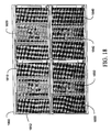
- Fig. 17 illustrates several screenshot 1700, 1710, 1720, and 1730 of a computer implemented program utilizing one embodiment of the present invention in which it is demonstrated that the comparison of a stepper image directly from the layout database and a stepper image simulated from the captured mask image may yield problem areas.
- the screenshot 1710 illustrates a captured microscope image of a portion of a mask while screenshot 1730 illustrates the simulated wafer exposure of the mask of screenshot 1710 under a particular set of DUV stepper conditions.
- Screenshot 1700 illustrates the original mask layout design of the portion of the mask shown in screenshot 1710, and screenshot 1720 illustrates the simulated wafer exposure of the original mask layout design of screenshot 1700 using the same stepper conditions as for the simulation displayed in screenshot 1730.
- areas 1732, 1734, and 1736 of screenshot 1730 it becomes apparent to an operator that there are problem areas to be considered. However, without the simulated mask exposure image these areas would not be as readily apparent as one would have to compare the captured mask image of screenshot 1710 with the original layout image of screenshot 1700. For when one compares areas 1712, 1714, and 1717 of screenshot 1710 to areas 1702, 1704, and 1706 of screenshot 1700, these problems are not as easily discovered.
- Fig. 18 illustrates a screenshot 1800 of a computer implemented program utilizing one embodiment of the present invention in which the mask being inspected has been OPC corrected.
- the screenshot 1800 comprises windows 1810, 1820, 1830, and 1840.
- Window 1830 illustrates an original layout of a portion of an OPC corrected mask with a small defect on an assist line as shown in area 1832.
- Window 1840 illustrates an original layout of a portion of the same OPC corrected mask but without the defect as shown in area 1842.
- Window 1810 illustrates the simulated wafer exposure of the mask of window 1830 under a particular set of stepper conditions.
- Window 1820 illustrates the simulated wafer exposure of the mask of window 1840 under the same set of stepper conditions.
- the small defect shown in area 1832 prints under the particular stepper conditions simulated in Fig. 18 .
- This small defect might be overlooked by conventionally used methods for inspecting OPC corrected masks.
- the OPC feature sliding tolerance scale used by some previous methods would not consider this slight deviation a defect if its size was smaller than the arbitrarily set scale.
- OPC features such as the defective assist line shown in area 1832, such small defects could print and therefore affect the operation of the end product circuit.
- FIG. 19 illustrates several screenshots 1900, 1910, and 1920 of a computer implemented program utilizing one embodiment of the present invention in which the effect of defects on the photolithography process window is demonstrated.
- the screenshot 1900 illustrates the simulated wafer exposure of a mask in which an area with no defect 1902 and two defect areas 1904 and 1906 are shown.
- Screenshot 1910 illustrates a simulated process window plot of Critical Dimension vs. Defocus for each of the areas 1902, 1904, and 1906, where data line 1 corresponds to the non defect area 1902, data line 2 corresponds to the defect area 1904, and data line 3 corresponds to defect area 1906.
- Line 1912 represents the user defined value of target CD for the mask, while lines 1914 and 1916 represent the upper and lower bounds of acceptable CD for the mask.
- the simulation illustrated in screenshot 1910 was performed for a lithography system with a Numerical Aperture of 0.50.
- Screenshot 1920 illustrates the same simulation as screenshot 1910, except that the Numerical Aperture of the simulated system was 0.42.
- a user can determine the range of acceptable defocus values of an exposure utilizing the mask under inspection. For instance, with respect to screenshots 1910 and 1920, the range of acceptable defocus values is that range within which the CD value of each of the three areas 1902, 1904, and 1906 falls within the upper and lower CD bounds 1914 and 1916.
- Fig. 20 illustrates another screenshot 2000 of a computer implemented program utilizing one embodiment of the present invention.
- the screenshot 2000 comprises windows 2010, 2020, 2030, 2040, 2050 and 2060.
- Window 2010 illustrates a captured microscope image of a portion of a mask with a defect in area 2012.
- Window 2020 illustrates the simulated wafer exposure of the mask of window 2010 under a particular set of stepper conditions, and shows the defect 2012 at area 2022.
- Window 2040 illustrates the original design layout of the captured mask image of window 2010.
- Window 2050 illustrates the simulated wafer exposure of the original design layout of window 2040 under the same particular set of stepper conditions.
- Window 2030 illustrates the difference between the simulated image of window 2020 and the simulated image of window 2050, and illustrates at area 2032 the overall effect of the defect 2012 on the design image.
- Window 2060 illustrates a 3D representation of the stepper image near the defect area.
Landscapes
- Physics & Mathematics (AREA)
- Engineering & Computer Science (AREA)
- General Physics & Mathematics (AREA)
- Theoretical Computer Science (AREA)
- Computer Hardware Design (AREA)
- Computer Vision & Pattern Recognition (AREA)
- Quality & Reliability (AREA)
- Evolutionary Computation (AREA)
- Geometry (AREA)
- General Engineering & Computer Science (AREA)
- Exposure And Positioning Against Photoresist Photosensitive Materials (AREA)
- Preparing Plates And Mask In Photomechanical Process (AREA)
- Investigating Materials By The Use Of Optical Means Adapted For Particular Applications (AREA)
Applications Claiming Priority (5)
| Application Number | Priority Date | Filing Date | Title |
|---|---|---|---|
| US5930697P | 1997-09-17 | 1997-09-17 | |
| US59306 | 1997-09-17 | ||
| US130996 | 1998-08-07 | ||
| US09/130,996 US6757645B2 (en) | 1997-09-17 | 1998-08-07 | Visual inspection and verification system |
| PCT/US1998/016742 WO1999014706A2 (en) | 1997-09-17 | 1998-08-11 | Visual inspection and verification system |
Publications (3)
| Publication Number | Publication Date |
|---|---|
| EP1012779A2 EP1012779A2 (en) | 2000-06-28 |
| EP1012779A4 EP1012779A4 (en) | 2007-10-17 |
| EP1012779B1 true EP1012779B1 (en) | 2009-10-07 |
Family
ID=26738616
Family Applications (1)
| Application Number | Title | Priority Date | Filing Date |
|---|---|---|---|
| EP98939366A Expired - Lifetime EP1012779B1 (en) | 1997-09-17 | 1998-08-11 | Method and system for lithographic mask inspection |
Country Status (7)
Cited By (2)
| Publication number | Priority date | Publication date | Assignee | Title |
|---|---|---|---|---|
| US8548223B2 (en) | 2010-01-18 | 2013-10-01 | Nuflare Technology, Inc. | Inspection system and method |
| US9057711B2 (en) | 2010-12-06 | 2015-06-16 | Nuflare Technology, Inc. | Inspection apparatus and method |
Families Citing this family (188)
| Publication number | Priority date | Publication date | Assignee | Title |
|---|---|---|---|---|
| US7093229B2 (en) * | 1997-09-17 | 2006-08-15 | Synopsys, Inc. | System and method for providing defect printability analysis of photolithographic masks with job-based automation |
| US7107571B2 (en) * | 1997-09-17 | 2006-09-12 | Synopsys, Inc. | Visual analysis and verification system using advanced tools |
| US7617474B2 (en) * | 1997-09-17 | 2009-11-10 | Synopsys, Inc. | System and method for providing defect printability analysis of photolithographic masks with job-based automation |
| US6757645B2 (en) * | 1997-09-17 | 2004-06-29 | Numerical Technologies, Inc. | Visual inspection and verification system |
| US6578188B1 (en) | 1997-09-17 | 2003-06-10 | Numerical Technologies, Inc. | Method and apparatus for a network-based mask defect printability analysis system |
| US6178360B1 (en) * | 1998-02-05 | 2001-01-23 | Micron Technology, Inc. | Methods and apparatus for determining optimum exposure threshold for a given photolithographic model |
| US6301697B1 (en) * | 1999-04-30 | 2001-10-09 | Nicolas B. Cobb | Streamlined IC mask layout optical and process correction through correction reuse |
| US6891967B2 (en) * | 1999-05-04 | 2005-05-10 | Speedline Technologies, Inc. | Systems and methods for detecting defects in printed solder paste |
| US7072503B2 (en) * | 1999-05-04 | 2006-07-04 | Speedline Technologies, Inc. | Systems and methods for detecting defects in printed solder paste |
| US6704695B1 (en) * | 1999-07-16 | 2004-03-09 | International Business Machines Corporation | Interactive optical proximity correction design method |
| US7391929B2 (en) | 2000-02-11 | 2008-06-24 | Sony Corporation | Masking tool |
| US7120285B1 (en) * | 2000-02-29 | 2006-10-10 | Advanced Micro Devices, Inc. | Method for evaluation of reticle image using aerial image simulator |
| JP2002107309A (ja) * | 2000-09-28 | 2002-04-10 | Toshiba Corp | 欠陥検査装置及び欠陥検査方法 |
| JP3266602B1 (ja) * | 2000-10-30 | 2002-03-18 | 洋一 奥寺 | アドレス照会システム、コンピュータプログラム製品及びその方法 |
| WO2002045014A2 (de) * | 2000-11-30 | 2002-06-06 | Sigma C Gmbh | Verfahren und vorrichtung zur bestimmung von eigenschaften einer integrierten schaltung |
| US6653026B2 (en) * | 2000-12-20 | 2003-11-25 | Numerical Technologies, Inc. | Structure and method of correcting proximity effects in a tri-tone attenuated phase-shifting mask |
| US6553559B2 (en) * | 2001-01-05 | 2003-04-22 | International Business Machines Corporation | Method to determine optical proximity correction and assist feature rules which account for variations in mask dimensions |
| US6602728B1 (en) * | 2001-01-05 | 2003-08-05 | International Business Machines Corporation | Method for generating a proximity model based on proximity rules |
| US6873720B2 (en) * | 2001-03-20 | 2005-03-29 | Synopsys, Inc. | System and method of providing mask defect printability analysis |
| US6816997B2 (en) * | 2001-03-20 | 2004-11-09 | Cheehoe Teh | System and method for performing design rule check |
| JP4663214B2 (ja) * | 2001-03-20 | 2011-04-06 | シノプシイス インコーポレイテッド | マスク欠陥のプリンタビリティ解析を提供するシステム及び方法 |
| US6925202B2 (en) | 2001-03-20 | 2005-08-02 | Synopsys, Inc. | System and method of providing mask quality control |
| US20030014146A1 (en) * | 2001-07-12 | 2003-01-16 | Kabushiki Kaisha Toshiba | Dangerous process/pattern detection system and method, danger detection program, and semiconductor device manufacturing method |
| JP4122735B2 (ja) * | 2001-07-24 | 2008-07-23 | 株式会社日立製作所 | 半導体デバイスの検査方法および検査条件設定方法 |
| US6560766B2 (en) | 2001-07-26 | 2003-05-06 | Numerical Technologies, Inc. | Method and apparatus for analyzing a layout using an instance-based representation |
| US6721928B2 (en) | 2001-07-26 | 2004-04-13 | Numerical Technologies, Inc. | Verification utilizing instance-based hierarchy management |
| EP1415320B1 (en) * | 2001-07-26 | 2006-11-02 | Koninklijke Philips Electronics N.V. | Method of measuring the performance of a scanning electron microscope |
| US7014955B2 (en) | 2001-08-28 | 2006-03-21 | Synopsys, Inc. | System and method for indentifying dummy features on a mask layer |
| US6670082B2 (en) | 2001-10-09 | 2003-12-30 | Numerical Technologies, Inc. | System and method for correcting 3D effects in an alternating phase-shifting mask |
| US6898596B2 (en) * | 2001-10-23 | 2005-05-24 | Therma-Wave, Inc. | Evolution of library data sets |
| US6976240B2 (en) * | 2001-11-14 | 2005-12-13 | Synopsys Inc. | Simulation using design geometry information |
| US7085698B2 (en) * | 2001-12-18 | 2006-08-01 | Synopsys, Inc. | Method for providing flexible and dynamic reporting capability using simulation tools |
| US6658640B2 (en) | 2001-12-26 | 2003-12-02 | Numerical Technologies, Inc. | Simulation-based feed forward process control |
| JP4138318B2 (ja) * | 2002-01-08 | 2008-08-27 | 株式会社ルネサステクノロジ | リソグラフィプロセスマージン評価装置、リソグラフィプロセスマージン評価方法およびリソグラフィプロセスマージン評価プログラム |
| AU2003201746A1 (en) * | 2002-01-15 | 2003-07-30 | Yissum Research Development Company Of The Hebrew University Of Jerusalem | System and method for compressing the dynamic range of an image |
| US6943810B2 (en) * | 2002-02-06 | 2005-09-13 | International Business Machines Corporation | Layered article data verification |
| US7257247B2 (en) * | 2002-02-21 | 2007-08-14 | International Business Machines Corporation | Mask defect analysis system |
| US7136796B2 (en) * | 2002-02-28 | 2006-11-14 | Timbre Technologies, Inc. | Generation and use of integrated circuit profile-based simulation information |
| US6745372B2 (en) | 2002-04-05 | 2004-06-01 | Numerical Technologies, Inc. | Method and apparatus for facilitating process-compliant layout optimization |
| US7085622B2 (en) * | 2002-04-19 | 2006-08-01 | Applied Material, Inc. | Vision system |
| US7233841B2 (en) * | 2002-04-19 | 2007-06-19 | Applied Materials, Inc. | Vision system |
| US6954911B2 (en) * | 2002-05-01 | 2005-10-11 | Synopsys, Inc. | Method and system for simulating resist and etch edges |
| DE10230532B4 (de) * | 2002-07-05 | 2007-03-08 | Infineon Technologies Ag | Verfahren zum Bestimmen des Aufbaus einer Maske zum Mikrostrukturieren von Halbleitersubstraten mittels Fotolithographie |
| DE10230755A1 (de) * | 2002-07-09 | 2004-01-22 | Carl Zeiss Jena Gmbh | Anordnung zur Herstellung von Photomasken |
| US6902855B2 (en) * | 2002-07-15 | 2005-06-07 | Kla-Tencor Technologies | Qualifying patterns, patterning processes, or patterning apparatus in the fabrication of microlithographic patterns |
| WO2004008244A2 (en) * | 2002-07-15 | 2004-01-22 | Kla-Tencor Technologies Corp. | Defect inspection methods that include acquiring aerial images of a reticle for different lithographic process variables |
| US6782525B2 (en) | 2002-09-05 | 2004-08-24 | Lsi Logic Corporation | Wafer process critical dimension, alignment, and registration analysis simulation tool |
| US7043071B2 (en) * | 2002-09-13 | 2006-05-09 | Synopsys, Inc. | Soft defect printability simulation and analysis for masks |
| US7149340B2 (en) * | 2002-09-20 | 2006-12-12 | Lsi Logic Corporation | Mask defect analysis for both horizontal and vertical processing effects |
| US7123356B1 (en) * | 2002-10-15 | 2006-10-17 | Kla-Tencor Technologies Corp. | Methods and systems for inspecting reticles using aerial imaging and die-to-database detection |
| JP2004157475A (ja) * | 2002-11-08 | 2004-06-03 | Toshiba Corp | 集積回路のパターン設計方法、露光マスクの作成方法、露光マスク、および集積回路装置の製造方法 |
| JP2004163348A (ja) * | 2002-11-15 | 2004-06-10 | Nippon Avionics Co Ltd | 検査状況表示方法 |
| US6768958B2 (en) | 2002-11-26 | 2004-07-27 | Lsi Logic Corporation | Automatic calibration of a masking process simulator |
| US7152219B2 (en) * | 2002-12-10 | 2006-12-19 | Synopsys Inc. | Reference image generation from subject image for photolithography mask analysis |
| US7131100B2 (en) * | 2002-12-10 | 2006-10-31 | Synopsys Inc. | Identifying phantom images generated by side-lobes |
| US7171047B2 (en) | 2002-12-20 | 2007-01-30 | Lsi Logic Corporation | Adaptive Sem edge recognition algorithm |
| US6996790B2 (en) * | 2003-01-30 | 2006-02-07 | Synopsys, Inc. | System and method for generating a two-dimensional yield map for a full layout |
| DE10316821A1 (de) * | 2003-04-03 | 2004-10-21 | Infineon Technologies Ag | Verfahren und Vorrichtung zur Korrektur von Abbildungsfehlern eines optischen Systems sowie eine Verwendung der Vorrichtung |
| US9002497B2 (en) * | 2003-07-03 | 2015-04-07 | Kla-Tencor Technologies Corp. | Methods and systems for inspection of wafers and reticles using designer intent data |
| US20050234684A1 (en) * | 2004-04-19 | 2005-10-20 | Mentor Graphics Corp. | Design for manufacturability |
| WO2005017997A1 (en) * | 2003-08-01 | 2005-02-24 | Applied Materials Israel, Ltd. | Charged particle beam inspection |
| US7558419B1 (en) | 2003-08-14 | 2009-07-07 | Brion Technologies, Inc. | System and method for detecting integrated circuit pattern defects |
| US8050900B2 (en) * | 2003-09-30 | 2011-11-01 | Tokyo Electron Limited | System and method for using first-principles simulation to provide virtual sensors that facilitate a semiconductor manufacturing process |
| US8032348B2 (en) * | 2003-09-30 | 2011-10-04 | Tokyo Electron Limited | System and method for using first-principles simulation to facilitate a semiconductor manufacturing process |
| US8073667B2 (en) * | 2003-09-30 | 2011-12-06 | Tokyo Electron Limited | System and method for using first-principles simulation to control a semiconductor manufacturing process |
| US8296687B2 (en) * | 2003-09-30 | 2012-10-23 | Tokyo Electron Limited | System and method for using first-principles simulation to analyze a process performed by a semiconductor processing tool |
| US8036869B2 (en) * | 2003-09-30 | 2011-10-11 | Tokyo Electron Limited | System and method for using first-principles simulation to control a semiconductor manufacturing process via a simulation result or a derived empirical model |
| US7003758B2 (en) | 2003-10-07 | 2006-02-21 | Brion Technologies, Inc. | System and method for lithography simulation |
| US7010776B2 (en) * | 2003-10-27 | 2006-03-07 | International Business Machines Corporation | Extending the range of lithographic simulation integrals |
| JP2005157043A (ja) * | 2003-11-27 | 2005-06-16 | Toshiba Corp | マスクパターン補正結果検証方法およびマスクパターン補正結果検証装置 |
| US8151220B2 (en) * | 2003-12-04 | 2012-04-03 | Kla-Tencor Technologies Corp. | Methods for simulating reticle layout data, inspecting reticle layout data, and generating a process for inspecting reticle layout data |
| US7069534B2 (en) | 2003-12-17 | 2006-06-27 | Sahouria Emile Y | Mask creation with hierarchy management using cover cells |
| JP2005189655A (ja) | 2003-12-26 | 2005-07-14 | Nec Electronics Corp | マスク検査方法 |
| KR101056142B1 (ko) * | 2004-01-29 | 2011-08-10 | 케이엘에이-텐코 코포레이션 | 레티클 설계 데이터의 결함을 검출하기 위한 컴퓨터로구현되는 방법 |
| US9188974B1 (en) | 2004-02-13 | 2015-11-17 | Kla-Tencor Technologies Corp. | Methods for improved monitor and control of lithography processes |
| US7162223B2 (en) * | 2004-02-17 | 2007-01-09 | Teamon Systems, Inc. | System and method for notifying users of an event using alerts |
| US7269804B2 (en) * | 2004-04-02 | 2007-09-11 | Advanced Micro Devices, Inc. | System and method for integrated circuit device design and manufacture using optical rule checking to screen resolution enhancement techniques |
| US7448012B1 (en) | 2004-04-21 | 2008-11-04 | Qi-De Qian | Methods and system for improving integrated circuit layout |
| JP2005309140A (ja) * | 2004-04-22 | 2005-11-04 | Toshiba Corp | フォトマスク製造方法、フォトマスク欠陥修正箇所判定方法、及びフォトマスク欠陥修正箇所判定装置 |
| JP2005317818A (ja) * | 2004-04-30 | 2005-11-10 | Dainippon Screen Mfg Co Ltd | パターン検査装置およびパターン検査方法 |
| EP1745373A4 (en) * | 2004-05-09 | 2009-04-15 | Mentor Graphics Corp | DEFEKTORT IDENTIFICATION FOR MICROELECTION MANUFACTURING AND VERIFICATION |
| CA2567280A1 (en) * | 2004-05-21 | 2005-12-01 | Pressco Technology Inc. | Graphical re-inspection user setup interface |
| US7475379B2 (en) * | 2004-06-23 | 2009-01-06 | International Business Machines Corporation | Methods and systems for layout and routing using alternating aperture phase shift masks |
| US7788629B2 (en) * | 2004-07-21 | 2010-08-31 | Kla-Tencor Technologies Corp. | Systems configured to perform a non-contact method for determining a property of a specimen |
| US7663741B2 (en) * | 2004-08-31 | 2010-02-16 | Asml Netherlands B.V. | Lithographic apparatus, device manufacturing method, calibration method and computer program product |
| JP4904034B2 (ja) * | 2004-09-14 | 2012-03-28 | ケーエルエー−テンカー コーポレイション | レチクル・レイアウト・データを評価するための方法、システム及び搬送媒体 |
| WO2006044426A2 (en) * | 2004-10-12 | 2006-04-27 | Kla-Tencor Technologies Corp. | Computer-implemented methods and systems for classifying defects on a specimen |
| US7400390B2 (en) * | 2004-11-29 | 2008-07-15 | Applied Materials, Israel, Ltd. | Inspection system and a method for aerial reticle inspection |
| US7729529B2 (en) * | 2004-12-07 | 2010-06-01 | Kla-Tencor Technologies Corp. | Computer-implemented methods for detecting and/or sorting defects in a design pattern of a reticle |
| DE102005032601A1 (de) * | 2005-01-07 | 2006-07-20 | Heidelberger Druckmaschinen Ag | Druckmaschine |
| JP4916116B2 (ja) * | 2005-02-01 | 2012-04-11 | 株式会社ホロン | パターン特定方法およびパターン特定装置 |
| DE102005009536A1 (de) * | 2005-02-25 | 2006-08-31 | Carl Zeiss Sms Gmbh | Verfahren zur Maskeninspektion im Rahmen des Maskendesigns und der Maskenherstellung |
| JP2006244073A (ja) * | 2005-03-02 | 2006-09-14 | Matsushita Electric Ind Co Ltd | 半導体設計装置 |
| US7356787B2 (en) * | 2005-04-06 | 2008-04-08 | Taiwan Semiconductor Manufacturing Co., Ltd. | Alternative methodology for defect simulation and system |
| US7305334B2 (en) * | 2005-05-24 | 2007-12-04 | International Business Machines Corporation | Methodology for image fidelity verification |
| US7853920B2 (en) * | 2005-06-03 | 2010-12-14 | Asml Netherlands B.V. | Method for detecting, sampling, analyzing, and correcting marginal patterns in integrated circuit manufacturing |
| US7369129B2 (en) * | 2005-06-13 | 2008-05-06 | Sap Aktiengesellschaft | Automated user interface testing |
| US7769225B2 (en) * | 2005-08-02 | 2010-08-03 | Kla-Tencor Technologies Corp. | Methods and systems for detecting defects in a reticle design pattern |
| JP2007071678A (ja) * | 2005-09-07 | 2007-03-22 | Hitachi High-Technologies Corp | 検査システム |
| US7676077B2 (en) | 2005-11-18 | 2010-03-09 | Kla-Tencor Technologies Corp. | Methods and systems for utilizing design data in combination with inspection data |
| US7570796B2 (en) | 2005-11-18 | 2009-08-04 | Kla-Tencor Technologies Corp. | Methods and systems for utilizing design data in combination with inspection data |
| US8041103B2 (en) | 2005-11-18 | 2011-10-18 | Kla-Tencor Technologies Corp. | Methods and systems for determining a position of inspection data in design data space |
| JP4860294B2 (ja) * | 2006-02-16 | 2012-01-25 | 株式会社日立ハイテクノロジーズ | 電子顕微鏡 |
| JP4572862B2 (ja) * | 2006-04-05 | 2010-11-04 | 富士ゼロックス株式会社 | 画像形成装置シミュレーション装置、画像形成装置シミュレーション方法及びプログラム |
| TW200746259A (en) * | 2006-04-27 | 2007-12-16 | Nikon Corp | Measuring and/or inspecting method, measuring and/or inspecting apparatus, exposure method, device manufacturing method, and device manufacturing apparatus |
| KR100699899B1 (ko) * | 2006-05-08 | 2007-03-28 | 삼성전자주식회사 | 집적회로 장치 제조용 마스크 검사 장치 및 그 검사 방법 |
| JP4205739B2 (ja) | 2006-07-26 | 2009-01-07 | エルピーダメモリ株式会社 | レチクルパターンの欠陥修正装置およびその修正方法 |
| JP4203089B2 (ja) * | 2006-09-11 | 2008-12-24 | 株式会社東芝 | キャリブレーション方法、検査方法、及び半導体装置の製造方法 |
| US7877722B2 (en) * | 2006-12-19 | 2011-01-25 | Kla-Tencor Corp. | Systems and methods for creating inspection recipes |
| WO2008086282A2 (en) | 2007-01-05 | 2008-07-17 | Kla-Tencor Corporation | Methods and systems for using electrical information for a device being fabricated on a wafer to perform one or more defect-related functions |
| US8611637B2 (en) | 2007-01-11 | 2013-12-17 | Kla-Tencor Corporation | Wafer plane detection of lithographically significant contamination photomask defects |
| JP2008177064A (ja) * | 2007-01-19 | 2008-07-31 | Hitachi High-Technologies Corp | 走査型荷電粒子顕微鏡装置および走査型荷電粒子顕微鏡装置で取得した画像の処理方法 |
| US8544064B2 (en) * | 2007-02-09 | 2013-09-24 | Sony Corporation | Techniques for automatic registration of appliances |
| US7716023B2 (en) * | 2007-02-13 | 2010-05-11 | Oracle America, Inc. | Multidimensional process corner derivation using surrogate based simultaneous yield analysis |
| DE102007000981B4 (de) * | 2007-02-22 | 2020-07-30 | Vistec Semiconductor Systems Gmbh | Vorrichtung und Verfahren zum Vermessen von Strukturen auf einer Maske und zur Berechnung der aus den Strukturen resultierenden Strukturen in einem Photoresist |
| US8335369B2 (en) * | 2007-02-28 | 2012-12-18 | Taiwan Semiconductor Manufacturing Company, Ltd. | Mask defect analysis |
| US7962863B2 (en) | 2007-05-07 | 2011-06-14 | Kla-Tencor Corp. | Computer-implemented methods, systems, and computer-readable media for determining a model for predicting printability of reticle features on a wafer |
| US7738093B2 (en) | 2007-05-07 | 2010-06-15 | Kla-Tencor Corp. | Methods for detecting and classifying defects on a reticle |
| US8213704B2 (en) | 2007-05-09 | 2012-07-03 | Kla-Tencor Corp. | Methods and systems for detecting defects in a reticle design pattern |
| US7818710B2 (en) * | 2007-07-03 | 2010-10-19 | Micron Technology, Inc. | Method and system for lithographic simulation and verification |
| KR100891336B1 (ko) * | 2007-07-05 | 2009-03-31 | 삼성전자주식회사 | 마스크 레이아웃 이미지의 생성 방법, 이를 수행하는프로그래밍된 명령을 저장하는 컴퓨터에서 판독 가능한저장 매체 및 이미징 시스템 |
| DE102007033243A1 (de) * | 2007-07-12 | 2009-01-15 | Carl Zeiss Sms Gmbh | Verfahren und Anordnung zur Analyse einer Gruppe von Photolithographiemasken |
| US7796804B2 (en) | 2007-07-20 | 2010-09-14 | Kla-Tencor Corp. | Methods for generating a standard reference die for use in a die to standard reference die inspection and methods for inspecting a wafer |
| US7711514B2 (en) | 2007-08-10 | 2010-05-04 | Kla-Tencor Technologies Corp. | Computer-implemented methods, carrier media, and systems for generating a metrology sampling plan |
| JP5425779B2 (ja) | 2007-08-20 | 2014-02-26 | ケーエルエー−テンカー・コーポレーション | 実際の欠陥が潜在的にシステム的な欠陥であるか、または潜在的にランダムな欠陥であるかを判断する、コンピューターに実装された方法 |
| US8068674B2 (en) * | 2007-09-04 | 2011-11-29 | Evolution Robotics Retail, Inc. | UPC substitution fraud prevention |
| KR101328611B1 (ko) * | 2007-10-19 | 2013-11-11 | 삼성전자주식회사 | 반도체 메모리 디바이스 제조를 위한 패턴 매칭 방법 |
| JP4554691B2 (ja) * | 2008-02-25 | 2010-09-29 | アドバンスド・マスク・インスペクション・テクノロジー株式会社 | 補正パターン画像生成装置、パターン検査装置および補正パターン画像生成方法 |
| US8139844B2 (en) | 2008-04-14 | 2012-03-20 | Kla-Tencor Corp. | Methods and systems for determining a defect criticality index for defects on wafers |
| US7995199B2 (en) * | 2008-06-16 | 2011-08-09 | Kla-Tencor Corporation | Method for detection of oversized sub-resolution assist features |
| KR101623747B1 (ko) | 2008-07-28 | 2016-05-26 | 케이엘에이-텐코어 코오포레이션 | 웨이퍼 상의 메모리 디바이스 영역에서 검출된 결함들을 분류하기 위한 컴퓨터-구현 방법들, 컴퓨터-판독 가능 매체, 및 시스템들 |
| JP2010107737A (ja) * | 2008-10-30 | 2010-05-13 | Toshiba Corp | マスク検証方法、半導体装置の製造方法及び露光条件の調整プログラム |
| JP5287178B2 (ja) * | 2008-11-27 | 2013-09-11 | 富士通セミコンダクター株式会社 | 欠陥レビュー装置 |
| US8775101B2 (en) | 2009-02-13 | 2014-07-08 | Kla-Tencor Corp. | Detecting defects on a wafer |
| US8204297B1 (en) | 2009-02-27 | 2012-06-19 | Kla-Tencor Corp. | Methods and systems for classifying defects detected on a reticle |
| US8112241B2 (en) | 2009-03-13 | 2012-02-07 | Kla-Tencor Corp. | Methods and systems for generating an inspection process for a wafer |
| US20110047519A1 (en) * | 2009-05-11 | 2011-02-24 | Juan Andres Torres Robles | Layout Content Analysis for Source Mask Optimization Acceleration |
| JP2011040560A (ja) * | 2009-08-11 | 2011-02-24 | Toshiba Corp | 発光解析装置および発光解析方法 |
| JP4942800B2 (ja) * | 2009-08-18 | 2012-05-30 | 株式会社ニューフレアテクノロジー | 検査装置 |
| US8166423B2 (en) * | 2009-09-08 | 2012-04-24 | International Business Machines Corporation | Photomask design verification |
| US9035673B2 (en) * | 2010-01-25 | 2015-05-19 | Palo Alto Research Center Incorporated | Method of in-process intralayer yield detection, interlayer shunt detection and correction |
| JP5695924B2 (ja) * | 2010-02-01 | 2015-04-08 | 株式会社ニューフレアテクノロジー | 欠陥推定装置および欠陥推定方法並びに検査装置および検査方法 |
| US8477299B2 (en) * | 2010-04-01 | 2013-07-02 | Taiwan Semiconductor Manufacturing Company, Ltd. | Method and apparatus for monitoring mask process impact on lithography performance |
| US8781781B2 (en) | 2010-07-30 | 2014-07-15 | Kla-Tencor Corp. | Dynamic care areas |
| CN102566291B (zh) * | 2010-12-29 | 2015-04-29 | 中芯国际集成电路制造(上海)有限公司 | 投影掩膜版的测试系统 |
| US8211717B1 (en) | 2011-01-26 | 2012-07-03 | International Business Machines Corporation | SEM repair for sub-optimal features |
| JP5603798B2 (ja) * | 2011-02-14 | 2014-10-08 | 株式会社キーエンス | 欠陥検出装置、欠陥検出方法及びコンピュータプログラム |
| US9170211B2 (en) | 2011-03-25 | 2015-10-27 | Kla-Tencor Corp. | Design-based inspection using repeating structures |
| JP5345169B2 (ja) * | 2011-03-25 | 2013-11-20 | 株式会社東芝 | マスク検査装置及びマスク検査方法 |
| JP2012252055A (ja) * | 2011-05-31 | 2012-12-20 | Toshiba Corp | マスク検査方法、マスク作製方法および半導体装置の製造方法 |
| CN103907109B9 (zh) | 2011-06-27 | 2017-02-22 | 耶路撒冷希伯来大学伊萨姆研究发展有限公司 | 为图像处理目的用滤波器应用卷积的快速数值逼近 |
| US9087367B2 (en) | 2011-09-13 | 2015-07-21 | Kla-Tencor Corp. | Determining design coordinates for wafer defects |
| US8831334B2 (en) | 2012-01-20 | 2014-09-09 | Kla-Tencor Corp. | Segmentation for wafer inspection |
| US8826200B2 (en) | 2012-05-25 | 2014-09-02 | Kla-Tencor Corp. | Alteration for wafer inspection |
| US20140064596A1 (en) | 2012-08-29 | 2014-03-06 | Micron Technology, Inc. | Descriptor guided fast marching method for analyzing images and systems using the same |
| US9189844B2 (en) | 2012-10-15 | 2015-11-17 | Kla-Tencor Corp. | Detecting defects on a wafer using defect-specific information |
| US8965102B2 (en) | 2012-11-09 | 2015-02-24 | Taiwan Semiconductor Manufacturing Company, Ltd. | System and method for defect analysis of a substrate |
| US9053527B2 (en) | 2013-01-02 | 2015-06-09 | Kla-Tencor Corp. | Detecting defects on a wafer |
| US9134254B2 (en) | 2013-01-07 | 2015-09-15 | Kla-Tencor Corp. | Determining a position of inspection system output in design data space |
| US9311698B2 (en) | 2013-01-09 | 2016-04-12 | Kla-Tencor Corp. | Detecting defects on a wafer using template image matching |
| KR102029645B1 (ko) * | 2013-01-14 | 2019-11-18 | 삼성전자 주식회사 | 맞춤형 마스크의 제조 방법 및 맞춤형 마스크를 이용한 반도체 장치의 제조 방법 |
| KR102019534B1 (ko) | 2013-02-01 | 2019-09-09 | 케이엘에이 코포레이션 | 결함 특유의, 다중 채널 정보를 이용한 웨이퍼 상의 결함 검출 |
| US9865512B2 (en) | 2013-04-08 | 2018-01-09 | Kla-Tencor Corp. | Dynamic design attributes for wafer inspection |
| US9310320B2 (en) | 2013-04-15 | 2016-04-12 | Kla-Tencor Corp. | Based sampling and binning for yield critical defects |
| TWI629469B (zh) * | 2013-05-14 | 2018-07-11 | 美商克萊譚克公司 | 用於整合之多遍檢測之方法、光罩檢測系統及非暫時性電腦可讀媒體 |
| CN103617170B (zh) * | 2013-10-23 | 2017-04-12 | 上海华力微电子有限公司 | 曝光机文件自动检查系统 |
| US9529255B2 (en) * | 2013-12-04 | 2016-12-27 | Taiwan Semiconductor Manufacturing Co., Ltd. | Image process method to improve mask inspection performance |
| US9478019B2 (en) * | 2014-05-06 | 2016-10-25 | Kla-Tencor Corp. | Reticle inspection using near-field recovery |
| EP2952963B1 (en) * | 2014-06-03 | 2020-12-30 | Commissariat A L'energie Atomique Et Aux Energies Alternatives | Method for calculating the metrics of an ic manufacturing process |
| US10312161B2 (en) * | 2015-03-23 | 2019-06-04 | Applied Materials Israel Ltd. | Process window analysis |
| KR102343850B1 (ko) | 2015-05-06 | 2021-12-28 | 삼성전자주식회사 | 광 근접 보정에서 공통의 바이어스 값을 이용하여 마스크를 제작하는 방법 |
| KR102294366B1 (ko) * | 2015-06-16 | 2021-08-27 | 에이에스엠엘 네델란즈 비.브이. | 결함 검증을 위한 방법들 |
| US10395361B2 (en) * | 2015-08-10 | 2019-08-27 | Kla-Tencor Corporation | Apparatus and methods for inspecting reticles |
| JP6840129B2 (ja) * | 2015-08-10 | 2021-03-10 | ケーエルエー コーポレイション | ウエハレベル欠陥の転写性を予測する装置および方法 |
| US10699971B2 (en) * | 2015-08-17 | 2020-06-30 | Qoniac Gmbh | Method for processing of a further layer on a semiconductor wafer |
| US10008422B2 (en) * | 2015-08-17 | 2018-06-26 | Qoniac Gmbh | Method for assessing the usability of an exposed and developed semiconductor wafer |
| JP6527808B2 (ja) | 2015-10-27 | 2019-06-05 | 株式会社ニューフレアテクノロジー | 検査方法および検査装置 |
| KR102387459B1 (ko) * | 2015-11-20 | 2022-04-15 | 삼성전자주식회사 | 반도체 소자의 패턴 형성 방법 |
| CN205556762U (zh) * | 2016-05-05 | 2016-09-07 | 鄂尔多斯市源盛光电有限责任公司 | 掩膜板、母板、掩膜板制造设备和显示基板蒸镀系统 |
| TWI755453B (zh) * | 2017-05-18 | 2022-02-21 | 美商克萊譚克公司 | 鑑定一光微影光罩合格性之方法及系統 |
| US10429314B2 (en) | 2017-07-31 | 2019-10-01 | Taiwan Semiconductor Manufacturing Co., Ltd. | EUV vessel inspection method and related system |
| US20200282654A1 (en) * | 2019-03-06 | 2020-09-10 | Owens-Brockway Glass Container Inc. | Repairing an Outer Surface of a Glass Product |
| JP7270417B2 (ja) * | 2019-03-08 | 2023-05-10 | キヤノン株式会社 | インプリント装置の制御方法、インプリント装置、および物品製造方法 |
| US11188212B2 (en) | 2020-03-19 | 2021-11-30 | Panasonic Intellectual Property Management Co., Ltd. | Methods and systems for monitoring objects for image-inspection |
| CN113009775A (zh) * | 2021-02-25 | 2021-06-22 | 广州粤芯半导体技术有限公司 | 光罩及光罩缺陷检查的方法 |
| CN113237888B (zh) * | 2021-05-21 | 2022-06-14 | 哈尔滨工业大学 | 大口径光学元件损伤点在线与离线暗场图像匹配方法 |
| JP2024532657A (ja) * | 2021-08-11 | 2024-09-10 | エーエスエムエル ネザーランズ ビー.ブイ. | マスク欠陥検出 |
| CN117132460B (zh) * | 2023-09-12 | 2024-02-27 | 上海世禹精密设备股份有限公司 | 视觉检测标准图的生成方法、装置、电子设备及存储介质 |
Family Cites Families (66)
| Publication number | Priority date | Publication date | Assignee | Title |
|---|---|---|---|---|
| US4812962A (en) | 1987-04-09 | 1989-03-14 | Harris Corp. | Area feature sorting mechanism for neighborhood-based proximity correction in lithography processing of integrated circuit patterns |
| US5182718A (en) | 1989-04-04 | 1993-01-26 | Matsushita Electric Industrial Co., Ltd. | Method and apparatus for writing a pattern on a semiconductor sample based on a resist pattern corrected for proximity effects resulting from direct exposure of the sample by a charged-particle beam or light |
| US5051598A (en) | 1990-09-12 | 1991-09-24 | International Business Machines Corporation | Method for correcting proximity effects in electron beam lithography |
| JPH04165353A (ja) | 1990-10-30 | 1992-06-11 | Oki Electric Ind Co Ltd | ホトマスク修正方法 |
| IL97022A0 (en) | 1991-01-24 | 1992-03-29 | Ibm Israel | Partitioning method for e-beam lithography |
| JP2974821B2 (ja) | 1991-06-19 | 1999-11-10 | 沖電気工業株式会社 | パターン形成方法 |
| DE69208413T2 (de) | 1991-08-22 | 1996-11-14 | Kla Instr Corp | Gerät zur automatischen Prüfung von Photomaske |
| US5563702A (en) * | 1991-08-22 | 1996-10-08 | Kla Instruments Corporation | Automated photomask inspection apparatus and method |
| US5242770A (en) | 1992-01-16 | 1993-09-07 | Microunity Systems Engineering, Inc. | Mask for photolithography |
| US5326659A (en) | 1992-03-05 | 1994-07-05 | Regents Of The University Of California | Method for making masks |
| CA2132005A1 (en) | 1992-04-06 | 1993-10-14 | Jang Fung Chen | Method for improved lithographic patterning in a semiconductor fabrication process |
| JP3730263B2 (ja) * | 1992-05-27 | 2005-12-21 | ケーエルエー・インストルメンツ・コーポレーション | 荷電粒子ビームを用いた自動基板検査の装置及び方法 |
| US5282140A (en) | 1992-06-24 | 1994-01-25 | Intel Corporation | Particle flux shadowing for three-dimensional topography simulation |
| US5256505A (en) | 1992-08-21 | 1993-10-26 | Microunity Systems Engineering | Lithographical mask for controlling the dimensions of resist patterns |
| US5538815A (en) | 1992-09-14 | 1996-07-23 | Kabushiki Kaisha Toshiba | Method for designing phase-shifting masks with automatization capability |
| EP0608657A1 (en) | 1993-01-29 | 1994-08-03 | International Business Machines Corporation | Apparatus and method for preparing shape data for proximity correction |
| JPH0728226A (ja) * | 1993-04-30 | 1995-01-31 | Internatl Business Mach Corp <Ibm> | 領域的イメージを測定する装置及び方法 |
| US5533148A (en) | 1993-09-30 | 1996-07-02 | International Business Machines Corporation | Method for restructuring physical design images into hierarchical data models |
| US5424154A (en) | 1993-12-10 | 1995-06-13 | Intel Corporation | Lithographic emhancement method and apparatus for randomly spaced structures |
| US5447810A (en) | 1994-02-09 | 1995-09-05 | Microunity Systems Engineering, Inc. | Masks for improved lithographic patterning for off-axis illumination lithography |
| GB2291219B (en) | 1994-07-05 | 1998-07-01 | Nec Corp | Photo-mask fabrication and use |
| US5573890A (en) | 1994-07-18 | 1996-11-12 | Advanced Micro Devices, Inc. | Method of optical lithography using phase shift masking |
| US5538833A (en) | 1994-08-03 | 1996-07-23 | International Business Machines Corporation | High resolution phase edge lithography without the need for a trim mask |
| JPH08297692A (ja) | 1994-09-16 | 1996-11-12 | Mitsubishi Electric Corp | 光近接補正装置及び方法並びにパタン形成方法 |
| JP3964469B2 (ja) | 1994-11-08 | 2007-08-22 | 株式会社東芝 | 形状シミュレーション方法 |
| US5532090A (en) | 1995-03-01 | 1996-07-02 | Intel Corporation | Method and apparatus for enhanced contact and via lithography |
| JP3409493B2 (ja) | 1995-03-13 | 2003-05-26 | ソニー株式会社 | マスクパターンの補正方法および補正装置 |
| US5553273A (en) | 1995-04-17 | 1996-09-03 | International Business Machines Corporation | Vertex minimization in a smart optical proximity correction system |
| US5657235A (en) | 1995-05-03 | 1997-08-12 | International Business Machines Corporation | Continuous scale optical proximity correction by mask maker dose modulation |
| US5663893A (en) | 1995-05-03 | 1997-09-02 | Microunity Systems Engineering, Inc. | Method for generating proximity correction features for a lithographic mask pattern |
| JP3331822B2 (ja) * | 1995-07-17 | 2002-10-07 | ソニー株式会社 | マスクパターン補正方法とそれを用いたマスク、露光方法および半導体装置 |
| US5825482A (en) | 1995-09-29 | 1998-10-20 | Kla-Tencor Corporation | Surface inspection system with misregistration error correction and adaptive illumination |
| WO1997013370A1 (en) | 1995-10-02 | 1997-04-10 | Kla Instruments Corporation | Alignment correction prior to image sampling in inspection systems |
| JP2917879B2 (ja) | 1995-10-31 | 1999-07-12 | 日本電気株式会社 | フォトマスク及びその製造方法 |
| JP3469422B2 (ja) | 1996-02-23 | 2003-11-25 | 株式会社東芝 | 荷電ビーム描画方法及び描画装置 |
| US5705301A (en) | 1996-02-27 | 1998-01-06 | Lsi Logic Corporation | Performing optical proximity correction with the aid of design rule checkers |
| US5801954A (en) | 1996-04-24 | 1998-09-01 | Micron Technology, Inc. | Process for designing and checking a mask layout |
| US5805290A (en) | 1996-05-02 | 1998-09-08 | International Business Machines Corporation | Method of optical metrology of unresolved pattern arrays |
| JP2776416B2 (ja) | 1996-05-07 | 1998-07-16 | 日本電気株式会社 | レチクル外観検査装置 |
| US5862058A (en) | 1996-05-16 | 1999-01-19 | International Business Machines Corporation | Optical proximity correction method and system |
| US5707765A (en) | 1996-05-28 | 1998-01-13 | Microunity Systems Engineering, Inc. | Photolithography mask using serifs and method thereof |
| US5740068A (en) | 1996-05-30 | 1998-04-14 | International Business Machines Corporation | Fidelity enhancement of lithographic and reactive-ion-etched images by optical proximity correction |
| US5849440A (en) | 1996-07-02 | 1998-12-15 | Motorola, Inc. | Process for producing and inspecting a lithographic reticle and fabricating semiconductor devices using same |
| US5795688A (en) * | 1996-08-14 | 1998-08-18 | Micron Technology, Inc. | Process for detecting defects in photomasks through aerial image comparisons |
| US6076465A (en) | 1996-09-20 | 2000-06-20 | Kla-Tencor Corporation | System and method for determining reticle defect printability |
| US5807649A (en) * | 1996-10-31 | 1998-09-15 | International Business Machines Corporation | Lithographic patterning method and mask set therefor with light field trim mask |
| US5917588A (en) | 1996-11-04 | 1999-06-29 | Kla-Tencor Corporation | Automated specimen inspection system for and method of distinguishing features or anomalies under either bright field or dark field illumination |
| US5804340A (en) | 1996-12-23 | 1998-09-08 | Lsi Logic Corporation | Photomask inspection method and inspection tape therefor |
| US5978501A (en) * | 1997-01-03 | 1999-11-02 | International Business Machines Corporation | Adaptive inspection method and system |
| US5847959A (en) | 1997-01-28 | 1998-12-08 | Etec Systems, Inc. | Method and apparatus for run-time correction of proximity effects in pattern generation |
| JP3750270B2 (ja) | 1997-04-21 | 2006-03-01 | 凸版印刷株式会社 | フォトマスク欠陥解析装置および欠陥解析方法 |
| JP3750272B2 (ja) | 1997-04-30 | 2006-03-01 | 凸版印刷株式会社 | フォトマスク欠陥解析装置および欠陥解析方法ならびに該欠陥解析プログラムを記録した記録媒体 |
| US6078738A (en) * | 1997-05-08 | 2000-06-20 | Lsi Logic Corporation | Comparing aerial image to SEM of photoresist or substrate pattern for masking process characterization |
| US6016357A (en) * | 1997-06-16 | 2000-01-18 | International Business Machines Corporation | Feedback method to repair phase shift masks |
| US6757645B2 (en) | 1997-09-17 | 2004-06-29 | Numerical Technologies, Inc. | Visual inspection and verification system |
| US7107571B2 (en) | 1997-09-17 | 2006-09-12 | Synopsys, Inc. | Visual analysis and verification system using advanced tools |
| US6011911A (en) | 1997-09-30 | 2000-01-04 | Synopsys, Inc. | Layout overlap detection with selective flattening in computer implemented integrated circuit design |
| US6009251A (en) | 1997-09-30 | 1999-12-28 | Synopsys, Inc. | Method and system for layout verification of an integrated circuit design with reusable subdesigns |
| US6009250A (en) | 1997-09-30 | 1999-12-28 | Synopsys, Inc. | Selective flattening in layout areas in computer implemented integrated circuit design |
| US5965306A (en) * | 1997-10-15 | 1999-10-12 | International Business Machines Corporation | Method of determining the printability of photomask defects |
| US6081658A (en) | 1997-12-31 | 2000-06-27 | Avant! Corporation | Proximity correction system for wafer lithography |
| US6282309B1 (en) * | 1998-05-29 | 2001-08-28 | Kla-Tencor Corporation | Enhanced sensitivity automated photomask inspection system |
| US6529621B1 (en) | 1998-12-17 | 2003-03-04 | Kla-Tencor | Mechanisms for making and inspecting reticles |
| US6301697B1 (en) | 1999-04-30 | 2001-10-09 | Nicolas B. Cobb | Streamlined IC mask layout optical and process correction through correction reuse |
| US6467076B1 (en) | 1999-04-30 | 2002-10-15 | Nicolas Bailey Cobb | Method and apparatus for submicron IC design |
| US6249904B1 (en) | 1999-04-30 | 2001-06-19 | Nicolas Bailey Cobb | Method and apparatus for submicron IC design using edge fragment tagging to correct edge placement distortion |
-
1998
- 1998-08-07 US US09/130,996 patent/US6757645B2/en not_active Expired - Lifetime
- 1998-08-11 EP EP98939366A patent/EP1012779B1/en not_active Expired - Lifetime
- 1998-08-11 KR KR1020007002870A patent/KR100596760B1/ko not_active Expired - Fee Related
- 1998-08-11 AU AU87809/98A patent/AU8780998A/en not_active Abandoned
- 1998-08-11 DE DE69841218T patent/DE69841218D1/de not_active Expired - Lifetime
- 1998-08-11 WO PCT/US1998/016742 patent/WO1999014706A2/en active IP Right Grant
- 1998-08-11 JP JP2000512171A patent/JP2001516898A/ja active Pending
-
2004
- 2004-06-28 US US10/878,847 patent/US7523027B2/en not_active Expired - Fee Related
Cited By (2)
| Publication number | Priority date | Publication date | Assignee | Title |
|---|---|---|---|---|
| US8548223B2 (en) | 2010-01-18 | 2013-10-01 | Nuflare Technology, Inc. | Inspection system and method |
| US9057711B2 (en) | 2010-12-06 | 2015-06-16 | Nuflare Technology, Inc. | Inspection apparatus and method |
Also Published As
| Publication number | Publication date |
|---|---|
| US20020019729A1 (en) | 2002-02-14 |
| US6757645B2 (en) | 2004-06-29 |
| EP1012779A2 (en) | 2000-06-28 |
| WO1999014706A2 (en) | 1999-03-25 |
| DE69841218D1 (de) | 2009-11-19 |
| AU8780998A (en) | 1999-04-05 |
| JP2001516898A (ja) | 2001-10-02 |
| US7523027B2 (en) | 2009-04-21 |
| KR100596760B1 (ko) | 2006-07-07 |
| KR20010024114A (ko) | 2001-03-26 |
| EP1012779A4 (en) | 2007-10-17 |
| US20040243320A1 (en) | 2004-12-02 |
| WO1999014706A3 (en) | 1999-05-06 |
Similar Documents
| Publication | Publication Date | Title |
|---|---|---|
| EP1012779B1 (en) | Method and system for lithographic mask inspection | |
| US7107571B2 (en) | Visual analysis and verification system using advanced tools | |
| US7003755B2 (en) | User interface for a networked-based mask defect printability analysis system | |
| US7117478B2 (en) | System and method for lithography simulation | |
| JP4216592B2 (ja) | 集積回路の特性を測定するプロセスと装置 | |
| US20060242619A1 (en) | System And Method For Providing Defect Printability Analysis Of Photolithographic Masks With Job-Based Automation | |
| US7469057B2 (en) | System and method for inspecting errors on a wafer | |
| US7665060B2 (en) | Approximating wafer intensity change to provide fast mask defect scoring | |
| US6999611B1 (en) | Reticle defect detection using simulation | |
| TW396393B (en) | Visual inspection and verification system | |
| Maenaka et al. | Defect printability analysis of attenuated PSM using PASStm |
Legal Events
| Date | Code | Title | Description |
|---|---|---|---|
| PUAI | Public reference made under article 153(3) epc to a published international application that has entered the european phase |
Free format text: ORIGINAL CODE: 0009012 |
|
| 17P | Request for examination filed |
Effective date: 20000403 |
|
| AK | Designated contracting states |
Kind code of ref document: A2 Designated state(s): DE FR GB IT |
|
| RAP1 | Party data changed (applicant data changed or rights of an application transferred) |
Owner name: NUMERICAL TECHNOLOGIES, INC. |
|
| RAP1 | Party data changed (applicant data changed or rights of an application transferred) |
Owner name: SYNOPSYS MERGER HOLDINGS LLC |
|
| RAP1 | Party data changed (applicant data changed or rights of an application transferred) |
Owner name: SYNOPSYS, INC. |
|
| A4 | Supplementary search report drawn up and despatched |
Effective date: 20070910 |
|
| RIC1 | Information provided on ipc code assigned before grant |
Ipc: G03F 7/20 20060101ALI20070904BHEP Ipc: G03F 1/00 20060101ALI20070904BHEP Ipc: G03F 9/00 20060101ALI20070904BHEP Ipc: G06T 7/00 20060101AFI20070904BHEP |
|
| 17Q | First examination report despatched |
Effective date: 20080506 |
|
| GRAP | Despatch of communication of intention to grant a patent |
Free format text: ORIGINAL CODE: EPIDOSNIGR1 |
|
| RTI1 | Title (correction) |
Free format text: METHOD AND SYSTEM FOR LITHOGRAPHIC MASK INSPECTION |
|
| GRAS | Grant fee paid |
Free format text: ORIGINAL CODE: EPIDOSNIGR3 |
|
| GRAA | (expected) grant |
Free format text: ORIGINAL CODE: 0009210 |
|
| AK | Designated contracting states |
Kind code of ref document: B1 Designated state(s): DE FR GB IT |
|
| REG | Reference to a national code |
Ref country code: GB Ref legal event code: FG4D |
|
| REF | Corresponds to: |
Ref document number: 69841218 Country of ref document: DE Date of ref document: 20091119 Kind code of ref document: P |
|
| PLBE | No opposition filed within time limit |
Free format text: ORIGINAL CODE: 0009261 |
|
| STAA | Information on the status of an ep patent application or granted ep patent |
Free format text: STATUS: NO OPPOSITION FILED WITHIN TIME LIMIT |
|
| 26N | No opposition filed |
Effective date: 20100708 |
|
| PGFP | Annual fee paid to national office [announced via postgrant information from national office to epo] |
Ref country code: FR Payment date: 20120823 Year of fee payment: 15 Ref country code: IT Payment date: 20120809 Year of fee payment: 15 |
|
| REG | Reference to a national code |
Ref country code: FR Ref legal event code: ST Effective date: 20140430 |
|
| PG25 | Lapsed in a contracting state [announced via postgrant information from national office to epo] |
Ref country code: IT Free format text: LAPSE BECAUSE OF NON-PAYMENT OF DUE FEES Effective date: 20130811 |
|
| PG25 | Lapsed in a contracting state [announced via postgrant information from national office to epo] |
Ref country code: FR Free format text: LAPSE BECAUSE OF NON-PAYMENT OF DUE FEES Effective date: 20130902 |
|
| PGFP | Annual fee paid to national office [announced via postgrant information from national office to epo] |
Ref country code: GB Payment date: 20170809 Year of fee payment: 20 Ref country code: DE Payment date: 20170808 Year of fee payment: 20 |
|
| REG | Reference to a national code |
Ref country code: DE Ref legal event code: R071 Ref document number: 69841218 Country of ref document: DE |
|
| REG | Reference to a national code |
Ref country code: GB Ref legal event code: PE20 Expiry date: 20180810 |
|
| PG25 | Lapsed in a contracting state [announced via postgrant information from national office to epo] |
Ref country code: GB Free format text: LAPSE BECAUSE OF EXPIRATION OF PROTECTION Effective date: 20180810 |