EP0923004A2 - Joint pour récipient de développateur, récipient de développateur, appareil de développement, unité de traitement et appareil de formation d'images - Google Patents
Joint pour récipient de développateur, récipient de développateur, appareil de développement, unité de traitement et appareil de formation d'images Download PDFInfo
- Publication number
- EP0923004A2 EP0923004A2 EP98310048A EP98310048A EP0923004A2 EP 0923004 A2 EP0923004 A2 EP 0923004A2 EP 98310048 A EP98310048 A EP 98310048A EP 98310048 A EP98310048 A EP 98310048A EP 0923004 A2 EP0923004 A2 EP 0923004A2
- Authority
- EP
- European Patent Office
- Prior art keywords
- seal
- developer
- electroconductive portion
- image forming
- container
- Prior art date
- Legal status (The legal status is an assumption and is not a legal conclusion. Google has not performed a legal analysis and makes no representation as to the accuracy of the status listed.)
- Granted
Links
Images


Classifications
-
- G—PHYSICS
- G03—PHOTOGRAPHY; CINEMATOGRAPHY; ANALOGOUS TECHNIQUES USING WAVES OTHER THAN OPTICAL WAVES; ELECTROGRAPHY; HOLOGRAPHY
- G03G—ELECTROGRAPHY; ELECTROPHOTOGRAPHY; MAGNETOGRAPHY
- G03G15/00—Apparatus for electrographic processes using a charge pattern
- G03G15/06—Apparatus for electrographic processes using a charge pattern for developing
- G03G15/10—Apparatus for electrographic processes using a charge pattern for developing using a liquid developer
-
- G—PHYSICS
- G03—PHOTOGRAPHY; CINEMATOGRAPHY; ANALOGOUS TECHNIQUES USING WAVES OTHER THAN OPTICAL WAVES; ELECTROGRAPHY; HOLOGRAPHY
- G03G—ELECTROGRAPHY; ELECTROPHOTOGRAPHY; MAGNETOGRAPHY
- G03G21/00—Arrangements not provided for by groups G03G13/00 - G03G19/00, e.g. cleaning, elimination of residual charge
- G03G21/16—Mechanical means for facilitating the maintenance of the apparatus, e.g. modular arrangements
- G03G21/18—Mechanical means for facilitating the maintenance of the apparatus, e.g. modular arrangements using a processing cartridge, whereby the process cartridge comprises at least two image processing means in a single unit
- G03G21/1803—Arrangements or disposition of the complete process cartridge or parts thereof
- G03G21/1828—Prevention of damage or soiling, e.g. mechanical abrasion
- G03G21/1832—Shielding members, shutter, e.g. light, heat shielding, prevention of toner scattering
-
- G—PHYSICS
- G03—PHOTOGRAPHY; CINEMATOGRAPHY; ANALOGOUS TECHNIQUES USING WAVES OTHER THAN OPTICAL WAVES; ELECTROGRAPHY; HOLOGRAPHY
- G03G—ELECTROGRAPHY; ELECTROPHOTOGRAPHY; MAGNETOGRAPHY
- G03G15/00—Apparatus for electrographic processes using a charge pattern
- G03G15/06—Apparatus for electrographic processes using a charge pattern for developing
- G03G15/08—Apparatus for electrographic processes using a charge pattern for developing using a solid developer, e.g. powder developer
- G03G15/0896—Arrangements or disposition of the complete developer unit or parts thereof not provided for by groups G03G15/08 - G03G15/0894
-
- G—PHYSICS
- G03—PHOTOGRAPHY; CINEMATOGRAPHY; ANALOGOUS TECHNIQUES USING WAVES OTHER THAN OPTICAL WAVES; ELECTROGRAPHY; HOLOGRAPHY
- G03G—ELECTROGRAPHY; ELECTROPHOTOGRAPHY; MAGNETOGRAPHY
- G03G21/00—Arrangements not provided for by groups G03G13/00 - G03G19/00, e.g. cleaning, elimination of residual charge
- G03G21/16—Mechanical means for facilitating the maintenance of the apparatus, e.g. modular arrangements
- G03G21/18—Mechanical means for facilitating the maintenance of the apparatus, e.g. modular arrangements using a processing cartridge, whereby the process cartridge comprises at least two image processing means in a single unit
- G03G21/1875—Mechanical means for facilitating the maintenance of the apparatus, e.g. modular arrangements using a processing cartridge, whereby the process cartridge comprises at least two image processing means in a single unit provided with identifying means or means for storing process- or use parameters, e.g. lifetime of the cartridge
-
- G—PHYSICS
- G03—PHOTOGRAPHY; CINEMATOGRAPHY; ANALOGOUS TECHNIQUES USING WAVES OTHER THAN OPTICAL WAVES; ELECTROGRAPHY; HOLOGRAPHY
- G03G—ELECTROGRAPHY; ELECTROPHOTOGRAPHY; MAGNETOGRAPHY
- G03G2215/00—Apparatus for electrophotographic processes
- G03G2215/08—Details of powder developing device not concerning the development directly
- G03G2215/0875—Arrangements for shipping or transporting of the developing device to or from the user
- G03G2215/0877—Sealing of the developing device opening, facing the image-carrying member
- G03G2215/088—Peelable sealing film
-
- G—PHYSICS
- G03—PHOTOGRAPHY; CINEMATOGRAPHY; ANALOGOUS TECHNIQUES USING WAVES OTHER THAN OPTICAL WAVES; ELECTROGRAPHY; HOLOGRAPHY
- G03G—ELECTROGRAPHY; ELECTROPHOTOGRAPHY; MAGNETOGRAPHY
- G03G2221/00—Processes not provided for by group G03G2215/00, e.g. cleaning or residual charge elimination
- G03G2221/16—Mechanical means for facilitating the maintenance of the apparatus, e.g. modular arrangements and complete machine concepts
- G03G2221/1648—Mechanical means for facilitating the maintenance of the apparatus, e.g. modular arrangements and complete machine concepts using seals, e.g. to prevent scattering of toner
-
- G—PHYSICS
- G03—PHOTOGRAPHY; CINEMATOGRAPHY; ANALOGOUS TECHNIQUES USING WAVES OTHER THAN OPTICAL WAVES; ELECTROGRAPHY; HOLOGRAPHY
- G03G—ELECTROGRAPHY; ELECTROPHOTOGRAPHY; MAGNETOGRAPHY
- G03G2221/00—Processes not provided for by group G03G2215/00, e.g. cleaning or residual charge elimination
- G03G2221/16—Mechanical means for facilitating the maintenance of the apparatus, e.g. modular arrangements and complete machine concepts
- G03G2221/1663—Mechanical means for facilitating the maintenance of the apparatus, e.g. modular arrangements and complete machine concepts having lifetime indicators
-
- G—PHYSICS
- G03—PHOTOGRAPHY; CINEMATOGRAPHY; ANALOGOUS TECHNIQUES USING WAVES OTHER THAN OPTICAL WAVES; ELECTROGRAPHY; HOLOGRAPHY
- G03G—ELECTROGRAPHY; ELECTROPHOTOGRAPHY; MAGNETOGRAPHY
- G03G2221/00—Processes not provided for by group G03G2215/00, e.g. cleaning or residual charge elimination
- G03G2221/16—Mechanical means for facilitating the maintenance of the apparatus, e.g. modular arrangements and complete machine concepts
- G03G2221/18—Cartridge systems
- G03G2221/183—Process cartridge
Definitions
- the present invention relates to a seal for sealing the opening of a developer container employed by a copying machine, a printer, or the like. It also relates to a developing container, a developing apparatus, a process cartridge, and an image forming apparatus.
- a container for storing developer has been employed in an electrophotographic apparatus, for example, an image forming apparatus, more specifically, a copying machine, a printer, or the like.
- This type of container is provided with an opening through which developer is discharged into a developing device.
- the opening is covered with a seal to prevent developer from leaking out of the container while the container filled with developer is transported.
- the seal is removed to expose the opening prior to the mounting of the container into the main assembly of an image forming apparatus.
- a developer container may constitute a part of a developing means container integral with a developing apparatus, or it may constitute a part of a process cartridge.
- the process cartridge comprises a photosensitive member as an image bearing member and a developing apparatus
- the developing apparatus integrally comprises the development container and a development device.
- the opening, through which developer is passed from the developer container to the developing means container is sealed with the aforementioned seal, and then, the seal is removed, that is, the developer container is unsealed, prior to the mounting of the process cartridge into an image forming apparatus.
- Detection of whether or not the seal has been removed has an additional merit in that the detection is analogous to detection of whether or not the developer container is brand new, and therefore, the detection makes it possible to accurately determine when the developer container is to be replaced next time; in other words, when a developer container constitutes a part of a process cartridge, it is possible to accurately determine when the process cartridge should be replaced.
- the primary object of the present invention is to provide a means for detecting whether or not a toner seal designed to be automatically removed has been removed.
- Another object of the present invention is to provide an inexpensive means for accurately detecting whether or not a toner seal has been removed.
- Another object of the present invention is to provide a means for detecting whether or not a developer container which has just been mounted in an image forming apparatus main assembly is brand new.
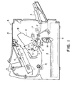
- Figure 1 is a vertical section of an image forming apparatus in the first embodiment of the present invention, and illustrates the locations and structures of the electrical contact points in the image forming apparatus.
- Figure 2 is a vertical cross section of a process cartridge in accordance with the present invention.
- Figure 3 is a front phantom view of a toner container, and depicts the toner container structure, and the toner seal.
- Figure 4 is a perspective view of the developing apparatus in the first embodiment of the present invention.
- Figure 5 is a perspective view of the developing apparatus in the first embodiment of the present invention.
- Figures 6, (a), (b) and (c) are circuit diagrams for the toner seal detecting means in the first embodiment of the present invention.
- Figure 7 is a plan of the toner seal in the second embodiment of the present invention, and depicts the toner seal structure.
- Figure 8 is a vertical section of the toner seal in the second embodiment of the present invention, and depicts the toner seal structure.
- Figure 9 is an enlarged plan of the electrically conductive portion of the toner seal in the second embodiment of the present invention.
- Figure 10 is a plan of the toner seal in the second embodiment of the present invention, which has been partially separated from the toner container.
- Figure 11 is an enlarged plan of the electrically conductive portion of the toner seal in the second embodiment of the present invention, and depicts the state of the toner seal which has been almost completely separated from the toner container.
- Figure 12 is an enlarged plan of the electrically conductive portion of the toner seal in the second embodiment of the present invention, and depicts the state of the toner seal at the end of its removal.
- Figure 13 is a plan of the toner seal in the third embodiment of the present invention, and depicts the structure thereof.
- Figure 14 is an enlarged plan of the electrically conductive portion of the toner seal in the third embodiment of the present invention.
- Figure 15 is a plan view of the toner seal in the third embodiment of the present invention, which has been thermally welded to the developer container.
- Figure 16 is an enlarged plan of the electrically conductive portion of the toner seal portion, at the end of the toner seal removal.
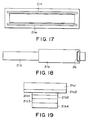
- Figure 17 is a plan of the toner seal after the completion of the toner seal removal in the sixth embodiment of the present invention.
- Figure 18 is a plan of the toner seal in the seventh embodiment of the present invention, and depicts the structure thereof.
- Figure 19 is a vertical cross section of the toner seal in the second embodiment of the present invention, and depicts the laminar structure thereof.
- Figure 20 is a perspective view of the developer container, the toner seal, and their adjacencies, in the second embodiment of the present invention, in which the toner seal has been fixed to the developer container.
- Figure 21 is a perspective view of the developer container, the toner seal, and their adjacencies, in the second embodiment of the present invention, in which the toner seal has been removed (complete removal).
- Figure 22 is a perspective view of the developer container, the toner seal, and their adjacencies, in the second embodiment of the present invention, in which the toner seal has been almost completely removed, with the end portion still remaining on the toner chamber frame.
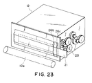
- Figure 23 is a perspective view of the developer container, the toner seal, and their adjacencies, in the third embodiment of the present invention, in which the toner seal has been fixed to the developer container.
- Figure 24 is a perspective view of the developer container in the third embodiment of the present invention, in which the toner seal has been almost completely removed.
- Figure 25 is a flow chart for the third embodiment.
- Figure 26 is an abbreviated circuit diagram for detecting the toner seal, in the third embodiment.
- Figure 27 is a perspective view of the developer container in the eighth embodiment of the present invention, to which the toner seal has been fixed after the filling of the developer into the developer container.
- FIG. 1 is a drawing which illustrates the general structure of the main assembly of an image forming apparatus, into which a process cartridge has been mounted.
- Figure 2 is a vertical section of the essential portion of the process cartridge, at the plane which runs perpendicular to the longitudinal direction of the process cartridge.
- the image forming apparatus A illustrated in Figure 1 is structured so that, as a cover 16 is opened, and a process cartridge is mounted into the main assembly of the image forming apparatus A, the electrodes 24e and 24f on the process cartridge side make contact with the electrodes 24ee and 24ff, respectively, on the main apparatus side of the image forming apparatus A.
- the image forming apparatus A also comprises an optical means 1, a manual feeding tray 3, an automatic sheet feeder roller 17, a transfer roller 4, a fixing means 5, a delivery tray 6, and a sheet discharge roller 15.
- the optical means 1 is positioned so that it will be above the process cartridge B after the mounting of the process cartridge B.
- the manual and automatic sheet feeder trays 3 and 7 are positioned to the right- and lefthand, respectively, of the cartridge space, and the transfer roller 4 is positioned below the process cartridge space.
- the fixing means 5 is positioned to the left of the transfer roller 4, and the delivery tray 6 and the sheet discharge roller 15 are positioned above the fixing means 5.
- the image forming apparatus A in this first embodiment of the present invention can also be fed with sheets of recording medium, with the use of a sheet cassette 9, which is positioned at the bottom of the image forming apparatus A main assembly as illustrated in Figure 1.
- the process cartridge B comprises a photosensitive drum 7 as an image bearing member which is rotatively driven, a charge roller 8 disposed immediately adjacent to the peripheral surface of the photosensitive drum 7, a developing means 10 which comprises a development sleeve 10a as a developer bearer, a cleaning apparatus 11, and the like, which are integrally assembled as a unit in the cartridge frame.
- the peripheral surface of the photosensitive drum 7 in the process cartridge B is uniformly charged by the charge roller 8, and a laser beam modulated with the image formation data from an original is projected from the optical means 1, upon the uniformly charged peripheral surface of the photosensitive drum 7, forming an electrostatic latent image on the peripheral surface of the photosensitive drum 7.
- the electrostatic latent image on the photosensitive drum 7 is developed into a toner image, that is, a visible image, with the use of toner, as developer, borne on the development sleeve 10a of the developing apparatus 10.
- pieces of recording medium 2 such as transfer sheet can be fed one by one into the main assembly of an image forming apparatus from either the manual feeder tray 3, or the cassette 9, by a feeder roller 17 or 18, respectively.
- the fed recording medium 2 passes between the peripheral surfaces of the photosensitive drum 7 and the transfer roller 4. While the recording medium 2 is passing between the photosensitive drum 7 and the transfer roller 4, the toner image on the photosensitive drum 7 is transferred onto the recording medium 2.
- the recording medium 2 After the transfer of the toner image onto the recording medium 2, the recording medium 2 is conveyed to the fixing means 5, in which the toner image is fixed to the recording medium 2 by heat and pressure. Thereafter, the recording medium 2 is discharged out of the image forming apparatus A into the delivery tray 6, being accumulated therein, by a discharge roller 15.
- the process cartridge B is constituted of a toner chamber frame 12 and a developing means frame 13, which are welded together along their top and bottom longitudinal edges by ultrasonic welding.
- the toner chamber frame 12 constitutes a developer container, and its opening 12a is sealed with a toner seal 12 after the developer container is filled with toner.
- the developing means frame 13 supports developing members such as the development sleeve 10a.
- the longitudinal ends of the process cartridge B in terms of the axial direction of the photosensitive drum 7 are sealed with an elastic seal.
- One of the elastic seals presses a tear tape 21b upon the toner chamber frame 12, at a slit 22 through which the toner seal is pulled out of the process cartridge B.
- Figures 4 and 5 are perspective views of the developer chamber frame 12, the developing apparatus 10, and their adjacencies.
- Figures 3 and 6 are plans of the developer chamber frame 12, as seen from its opening 12a side.
- FIGS 3 and 4 are drawings which illustrate the toner chamber frame 12, with its opening 12a sealed with the toner seal 21.
- the toner seal consists of a cover film 21a, that is, the portion of the toner seal 21 which actually covers the opening 12a, and a tear tape 21b, that is, the portion which has a length of no less than twice the length of the cover film 21a in terms of the longitudinal measurement of the cover film 21a, and is used to tear away the cover film 21.
- the cover film 21a is fixed to the periphery 12b of the opening 12a.
- the tear tape laminated to the cover film 21a is thermally adhered, together with the cover film 21a, to the toner chamber frame 12, by the so-called boat-shaped portions 21c and 21d, at both longitudinal ends of the toner chamber frame 12.
- the tear tape 21b is folded back at the deep end in terms of the direction indicated by an arrow mark Y in which the toner seal 21 is pulled away, and is caused to project outward from the slit 22.
- Figure 4 is a drawing which depicts the structure of the means for reeling the toner seal
- Figure 5 is a drawing which illustrates the toner seal 21 which has been removed, or reeled away.
- the development sleeve 10a is provided with development sleeve gears 10b and 10c, which are fixed to one of the longitudinal ends of the development sleeve 10a, and the other, respectively.
- the development gear 10b is meshed with the aforementioned drum gear 7a, and the development sleeve gear 10b is meshed with an unillustrated idler gear.
- the development sleeve gear 10b meshed with the drum gear 7a is driven, which in turn drives the development sleeve gear 10c along with the development sleeve gear 10b.
- the development sleeve gear 10c drives the bevel gear 20a through the unillustrated idler gear.
- the driving force is transmitted to the reeling shaft 20 coaxial with the bevel gear 20a, rotating the reeling shaft 20.
- the toner seal 21 is wound around the peripheral surface of the reeling shaft while being guided by the guiding portion 19a of the aforementioned idler roller 19.
- the reeling shaft 20 is provided with guides 20b, so that the toner seal 21 is prevented from being wound around the peripheral surface of the reeling shaft 20, on the portion other than the designated portion. Consequently, the cover film 21a is torn away from the toner chamber frame 12, from the deeper end, in terms of the direction in which the toner seal 21 is pulled, exposing the opening 12a.
- Figure 4 is a perspective view of the toner chamber frame 12 of the process cartridge B in this embodiment, in which the opening 12a of the toner chamber frame 12 is sealed with the toner seal 21, and the developing means frame 13 is not shown.
- the material for the toner seal 21 usage of laminated sheet composed of aluminum film and polyethylene-terephthalate (PET) film has been proposed. Also in this embodiment, this laminated sheet composed of the layers of aluminum film and PET film is employed.
- the toner seal 21 is provided with a guiding means (for example, provision of shallow cut in the surface of the toner seal 21).
- the toner seal 21 is provided with electrical contact points 24C and 24d, which are positioned on the area which is not reeled away by the reeling shaft 20, and remains on the toner chamber frame 12 side after the major portion of the toner seal 21 is reeled away by the reeling shaft 20 to expose the opening 12a. These contacts 24c and 24d will be described later.
- the toner seal 21 As the toner seal 21 is reeled away, two portions (electrical contact point 24c side and electrical contact point 24d side) of the toner seal 21 remain adhered to the toner chamber frame 12, on the opposite sides across the opening 12a.
- the electrical contact points 24c and 24d are positioned on the toner seal 21, on the separate portions, one for one, which remain adhered to the toner chamber frame 12, on the opposite sides of the opening 12a in terms of the width direction of the opening 12a, even after the removal of the major portion of the toner seal 21, so that the electrical connection between the two electrical contact points 24c and 24d is broken as the cover film 21a of the toner seal 21 is torn away.
- the PET film has been removed from the two portions of the cover film 21a, to which the aforementioned electrical contact points 24c and 24d are to be attached, respectively, to expose the aluminum film.
- elastic steel plate electrodes 26a and 26b are placed in contact, pressing down upon the electrical contact points 24c and 24d, and consequently, pressing indirectly upon the toner seal 21.
- This arrangement establishes electrical connection between the elastic steel plate electrodes 26a and 26b through the electrical contact point 24c, the aluminum film, and the electrical contact point 24d.
- the other ends of the elastic steel plate electrodes 26a and 26b are routed out of the toner chamber frame 12, and constitute electrical contact points 24e and 24f, with which the detecting means on the image forming apparatus main assembly side is electrically connected.
- the elastic steel electrodes 26a and 26b are fixed to the toner chamber frame 12, and are sealed with unillustrated seals formed of, for example, Moltplane, to prevent the toner from leaking out of the toner chamber frame 12.
- the main assembly side of the image forming apparatus is provided with electrical contact points 24ee and 24ff, so that electrical connection is established between the aforementioned electrical contact points 24c and 24d and the main assembly side as the process cartridge is mounted into the main assembly.
- Figure 6, (a), (b) and (c) are schematic drawings of the toner seal, and the electrical contact points 24c and 24d inclusive of their electrical connection.
- Figure 6, (a) depicts their states prior to, or at the time when, the reeling of the toner seal 21 begins, and
- Figure 6, (b) depicts their states while the toner seal 21 is being reeled away.
- Figure 6, (c) depicts their states after the completion of the reeling of the toner seal 21.
- the electrical contact points 24c and 24d are electrically connected through the electrically conducive aluminum film layer of the laminated toner seal 21.
- difference in electrical potential is provided between the aforementioned electrical contact points 24c and 24d with the use of direct current power source 25a, and whether or not the toner seal 21 of the process cartridge B has been completely reeled is detected by measuring the amount of current which flows between the electrical contact points 24c and 24d, with the use of a monitor 25b.
- a process cartridge is brand new, that is, has never been used, or it has been unsealed and in use, by detecting whether or not the toner seal 21 is present.
- the detecting means 25 inclusive of the direct current power source 25a and the monitor 25b is provided on the main assembly side of the image forming apparatus, and signalizes the result of the detection as to whether or not the toner seal 21 of the process cartridge B has been completely reeled.
- the signalized information is used to determine the length of the remaining service life of the process cartridge B as will be described below.
- the cumulative data of the process cartridge B for example, the cumulative number of rotations of the photosensitive drum 7 of the process cartridge B, the cumulative number of the pieces of recording medium 2 passed through the apparatus A, the print ratio, and the like, are stored on the image forming apparatus A side. Further, the image forming apparatus A main assembly is provided with a means (unillustrated) for displaying the length of the remaining service life and current state of the process cartridge B, to an operator.
- the means for detecting the length of the remaining service life of the process cartridge B counts the cumulative number of developed picture elements, calculates the cumulative amount of the consumed toner based on the cumulative number of the developed picture elements, and then, determines the length of the remaining service life of the process cartridge based on the cumulative amount of the consumed toner.
- the process cartridge B usage data which had been accumulated on the image forming apparatus main assembly side are treated as the data regarding the process cartridge B which has just been mounted into the image forming apparatus A, and the data obtained from this just mounted process cartridge B are cumulatively added to the process cartridge data which had been accumulated.
- the storage which had been storing the process cartridge usage data is reset, and begins to store the fresh data.
- the reeling shaft 20 is indirectly driven through an unillustrated gear train, and the structural components of the process cartridge (in the above embodiment, the development sleeve 10a is provided with the gear 10c), by an unillustrated driving power source on the image forming apparatus main assembly side.
- the reeling shaft 20 may be disposed within the process cartridge B, and directly connected to a driving power source within or outside the process cartridge B.
- the toner seal in the above embodiment was of a type with a tear tape.
- the toner seal may be of a type with no tear tape, that is, an easy-peel type which is entirely peeled off from the toner container.
- the present invention is also applicable to the toner seal of an easy-peel type.
- the electroconductive portion for unsealing detection of the seal portion is provided on the whole surface of the seal portion, but in this embodiment, it is provided in a part thereof.
- FIGS 7, 8 show a developer seal 21 as a seal member for sealing the opening of the developer accommodating container 12
- the layer structure of the seal base in this example are, from the surface layer side:
- a tearing portion 21e for unsealing is subjected to a carbon dioxide gas laser from the sealant layer side, so that polyester layer (tearing guide layer) and the sealant layer partly melts to form void portion or cavity by a laser cutting process.
- Figure 8 is a sectional view of the seal member, and shows the gap 21h provided by the laser machining).
- the aluminum foil layer blocks the laser, so that sufficient sealing property is assured without damage to the outermost surface polyester layer.
- the stress is concentrated at the gap formed by the laser machining process, and therefore, it can be assuredly torn and unsealed along the tearing portion 21e.
- an electroconductive portion 26 for unsealing detection is provided at an end of the developer discharging opening of the developer accommodating container (immediately before the ending portion of the unsealing).
- the electroconductive portion 26 is of aluminum foil with adhesive material (aluminum foil 30 ⁇ m and adhesive material 50 ⁇ m), and is pasted on the surface of the seal base.
- the electroconductive portion 26, as shown in Figure 9, is extended in a width direction which is perpendicular to the unsealing direction (direction indicated by the arrow in Figure 9 (enlarged view)) of the developer seal, and has contact portions 26a at the end thereof.
- the contact portions 26a are disposed outside the tearing portion 21e which is removed upon the unsealing of the developer seal, and therefore, are not removed but remains on the accommodating container after completion of the unsealing.
- the contact portions 26a are contacted to contacts (unshown) of a developing device, developer hopper or the like which receives the developer accommodating container, by which the electrical connection is established as shown in Figure 1.
- the width of the electroconductive portion 26 is 2mm, and the length in the lateral direction is approx. 50mm.
- Figure 20 shows the assembled state of the developer accommodating container with the developer seal of this example.
- FIGS 10, 11 and 12 show the unsealing operation of the developer seal of this example.
- Figure 10 shows the state during unsealing.
- a force receiving portion 21f is pulled in the fold-back direction (direction indicated by the arrow in Figure 10), so that sealing portion 21g is torn along the unsealing tearing portion 21e with the width substantially the same as the width of the developer discharging opening.
- Figure 11 shows in an enlarged scale a state wherein the electroconductive portion 26 at the end portion of the developer discharging opening is being torn, and
- Figure 12 shows in an enlarged scale the state after the sealing.
- the seal member may be wound up or may not be wound up, and as shown in Figure 21, upon the completion of the unsealing, the seal member may be completely removed, or as shown in Figure 22, pulling of the seal may be stopped after detecting the unsealing, so that end portion of the seal member may remain, depending on the structure of the main assembly of the image forming apparatus using the developer accommodating container of this example.
- the pulling of the seal in the case that after the detection of the unsealing, the pulling of the seal is stopped to leave the end of the seal member, the pulling of the seal can be stopped before an end portion Xl of a heat welded portion X of the seal member relative to the developer accommodating container is removed. In this case, it is not necessary to remove the end portion of the heat welded portion, and therefore, the required unsealing force is smaller than when the seal member is completely torn and removed.
- the electroconductive portion 26 of this example uses a pasted aluminum foil.
- the electric resistance value thereof will be considered.
- the electric resistance value of the electroconductive portion for the detection of conduction if the voltage applied across it by the voltage source 25a of the main assembly of the image forming apparatus can be high, the resistance value may be large. However, the high voltage is not desirable from the safety and cost, and therefore, the electric resistance value is preferably small to permit use of low voltage, more particularly, not more than 100 ⁇ , and preferably 10 ⁇ .
- the electroconductive portion 26 of this example has an electric resistance value of 1 ⁇ , and sufficient conduction is provided before cutting. After the cut, the electric resistance is infinite, i.e. Non-conductive.
- the low electric resistance value capable assuring sufficient conduction before the cut is preferable, and any material satisfying this, such as copper, nickel or other metal foil is usable.
- the aluminum foil is normally enough to provide sufficient conductivity, but due to the oxidation of the surface of the foil, the electric resistance value may become too high.
- the surface may preferably be provided with anti-oxidation layer such as carbon, nickel such as to assure the unsealing detection.
- the electroconductive portion 26 has to be torn along the tearing portion 21e of the developer seal. If it is not torn with small force and with certainty, the unsealing force is so high that entirety of the foil is pulled out, and is stuck on the other part or it falls.
- the material, the width, the thickness and the like of the electroconductive portion are preferably taken into account, with the fact that width or thickness are decreased, the electric resistance value tends to increase in mind.
- the aluminum foil of this example has the width of 2mm, the thickness of 30 ⁇ m and the electric resistance value of 1 ⁇ , with which the force required for tearing it is 0.1-0.2kgf which is sufficiently small.
- the electroconductive portion 26 of this example is pasted on the surface of the developer seal before welding of the developer seal onto the developer accommodating container or after that, but when it is pasted before the welding, the electroconductive member preferably has a heat-resistivity.
- the member including the contact portion is preferably simplified. In this example, it is pasted after the welding. No problem with the pasting was confirmed since the electroconductive member has a channel-like cross-section. More simple structure is usable.
- the adhesive material is used in this example, but double coated tape, another bonding or welding method is usable.
- the electroconductive portion on the surface of the seal base of the developer seal includes the unsealing detection electroconductive portion of Embodiment 2 and a mounting detection electroconductive portion for detecting mounting of the developer accommodating container at the correct position.
- the developer seal structure, the material of the electroconductive portions, and the bond onto the surface of the seal base or the like, are the same as with Embodiment 2.
- FIG 13 The developer seal of this example is shown in Figure 13.
- the inside one 26b is the unsealing detection electroconductive portion
- the outside one 26c is the mounting detection electroconductive portion.
- Figure 14 is an enlarged view of the electroconductive portion. Therefore, the upstream is for unsealing detection 26b, and the downstream is for mounting detection 26c with respect to the unsealing direction (direction indicated by the arrow in Figure 14).
- the two electroconductive portions for the unsealing detection and the mounting detection are extended in the lateral direction perpendicular to the unsealing direction, similarly to Embodiment 2.
- the contact portions 26a one 26al is common, and at the other side, it is separated into portions 26a2 and 26a3.
- the contacts 26al may be provided separately, the number of contacts is increased with the possible result of cost rise or poor assembling property.
- a common contact for 26a2, 26a3, is not usable, since then the use of two lines is meaningless.
- the unsealing detection electroconductive portion 26b is disposed at an end portion of the developer discharging opening, and the mounting detection electroconductive portion 26c is disposed further outside (downstream).
- the unsealing detection electroconductive portion is torn substantially simultaneously with full opening of the developer discharging opening, the conduction of the unsealing detection electroconductive portion (26al-26a2) is broken, so that unsealing state is detected, and at this time, the unsealing operation of the seal is stopped.
- the unsealing operation of the seal may be manual or automatic, and the seal may be wound up or may not be wound up.
- the automatic winding is preferably used, and the winding shaft drive is stopped immediately after the unsealing detection, and the unsealing operation is stopped before the mounting detection electroconductive portion. This is preferable.
- Figure 24 shows the state upon completion of the developer seal winding.
- Figure 16 is an enlarged view of the electroconductive portion when the developer seal has been unsealed.
- the unsealing detection electroconductive portion 26b is cut, but the mounting detection electroconductive portion 26c is maintained in the same state, so that conduction thereof (26a1-26a3) is kept.
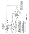
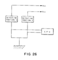
- Figure 25 is a flow chart of the foregoing operation, and Figure 26 schematically shows a circuit of the main assembly of the image forming apparatus.
- the detection portion 2 detects whether the mounting detection electroconductive portion (electroconductive portion 2) is conductive or not, if not, "no container" is displayed on the main assembly.
- the detection portion 1 detects or discriminates whether the unsealing detection electroconductive portion(electroconductive portion 1) is conductive or not, and if not, the conduction of the electroconductive portion 2 is checked, and if it is not conductive, the same display is made on the same assembly, and if it is conductive, completion of unsealing of the toner seal is discriminated.
- the electroconductive portion 1 is conductive, the winding of the toner seal is started, and the end of the unsealing is discriminated when the unsealing is detected upon the cut of the electroconductive portion 1.
- the detection portions 1 and 2 may be the same as the detecting means 25 of Figure 6.
- the mounting detection electroconductive portion is effective to detect correct mounting of the main body of the developer accommodating container, the developing device or the process cartridge which incorporates the developer accommodating container, relative to the image forming apparatus. Particularly, when the developer seal is wound up, the winding shaft (unshown) disposed adjacent the end of the seal and the mounting detection electroconductive portion are close to each other, and therefore, the correct mounting position can be assured with higher certainty than in the connection between the winding shaft and the driving gear.
- the unsealing detection position and the mounting detection position are close to each other on the developer seal, and therefore, as described hereinbefore, the contact portion can be shared partly, and simultaneous assembling is possible, with the advantage in terms of assembling and manufacturing cost.
- the unsealing confirmation tests of the developer accommodating container using the developer sealing member have been carried out, and it has been confirmed that unsealing strength of the electroconductive portion is as small as 0.2-0.3kgf including the developer seal per se, and that unsealing detection is stable.
- the mounting detection function is sufficient, and when the developer accommodating container is obliquely or inclinedly mounted, the conduction at the mounting detection portion is not established so that operation of the main assembly of the image forming apparatus including the driving of the winding shaft can be stopped, and damage of the winding shaft and the gear such as can be avoided.
- Embodiment 2 This example is similar to Embodiment 2, but the electroconductive portion for the unsealing detection is formed on the seal base by aluminum evaporation.
- the used developer seal, the developer accommodating container, the configuration pattern of the electroconductive portion 26, are the same as with Embodiment 2.
- Metal aluminum is evaporated on the polyester layer (surface layer) into a thickness of 600 angstrom to provide an electroconductive portion 26.
- the electric resistance value of the electroconductive portion is approx. 10 ⁇ , the unsealing detection was correctly performed.
- the film thickness can be small; the material cost is low, the tearing force is small; and the positional accuracy of assembling can be easily enhanced, although the cost for the manufacturing apparatus including masking for the evaporation pattern formation is high.
- the unsealing confirmation tests of the developer accommodating container using the developer sealing member have been carried out, and the unsealing strength of the electroconductive portion is slightly low (0.1-0.2kgf), and therefore, it is satisfactory. It has been also confirmed that unsealing detection is correct.
- Embodiment 3 can be incorporated in Embodiment 3. Even if the electroconductive portions for the unsealing detection and the mounting detection of Embodiment 3 are formed using aluminum evaporation, the results are satisfactory.
- Embodiment 2 This example is similar to Embodiment 2, but the electroconductive portion for the unsealing 5 detection is of carbon coating.
- the used developer seal, the developer accommodating container, the configuration pattern of the electroconductive portion 26, are the same as with Embodiment 2. More particularly, film is coated with material made of carbon black (ketchen black EC), thermoplastic elastomer (binder) (more particularly styrene and ethylene butylene block copolymer resin material), dispersed and mixed in toluene (solvent), which material is applied on the film and dried.
- carbon black ketchen black EC
- thermoplastic elastomer binder
- solvent toluene
- film formation and film thickness of the coating are important. More particularly, in order to firmly form the coating film, it is good to increase the amount of the binder, but if the amount of carbon is reduced correspondingly, the electric resistance value becomes large. As regards the film thickness of the coating, it is preferably as small as possible to decrease the tearing force, but reduction thereof results in the decrease of the amount or content of the carbon, and therefore, the electric resistance value increases. If the carbon content is increased in an attempt to prevent it, the formation of the coating film becomes difficult (poor circulation), so proper selection of the materials and the coating thickness are desired.
- thermoplastic elastomer 100 parts and carbon black 50 parts are mixed and dispersed in toluene solvent.
- the material is applied into film thickness 30 ⁇ m.
- the electric resistance value was approx. 100 ⁇ which is usable.
- the addition of carbon black was doubled, but no good film was formed.
- Embodiment 2 This example is similar to Embodiment 2, but the electroconductive member covers the entire surface of the developer seal. More particularly, aluminum foil is bonded on the entire surface of the polyester layer (surface layer) shown by 21i in Figure 8.
- the seal structure and the developer accommodating container or the like except for the polyester layer are the same as with Embodiment 2.
- the aluminum foil is bonded or pasted on the whole surface, the electric resistance is lower than in Embodiment 2 and is stable at a low level, thus assuring the unsealing detection.
- the latitude of the alignment is expanded. (the contact portion may be provided at any position of 21m and 21n in Figure 17). Additionally, it is pasted on all the surface, the assembling in the seal manufacturing is easy, and therefore, the manufacturing cost is low.
- the unsealing strength (force required for the unsealing) tends to be high, since the aluminum foil is added to the whole surface of the film.
- the forming method of the electroconductive portion in this example may be that of Embodiment 4 (evaporation of aluminum or the like) or carbon coating (Embodiment 5).
- Embodiment 4 evaporation of aluminum or the like
- Embodiment 5 carbon coating
- Embodiment 2 This is similar to Embodiment 2, but the developer seal comprising a cover film for sealing the developer discharging opening used in Embodiment 1 and a tear tape, lined on the cover film, which permits tearing of the cover film to form the opening.
- the structures of the developer accommodating container and the electroconductive portion for the unsealing detection, the fixing method on the seal member or the like are the same as with Embodiment 2.
- the layer structure preferably comprises:
- the cover film 21a for sealing the developer discharging opening comprises:
- the tear tape 21b for forming the opening preferably comprises the layer structure of the following:
- cover film and the tear tape are unified by welding to provide a seal member (between 21a2 and 21b1), and similarly to Embodiment 1, it is heat-welded to the edge portion of the opening of the developer accommodating container.
- seal member between 21a2 and 21b1
- aluminum foil is pasted on the surface of the seal as an electroconductive portion 26, similarly to Embodiment 2.
- the cover film is torn along the width of the tear tape.
- the unsealing advances until the electroconductive portion provided at the end of the developer discharging opening, is torn with the cover film, the electroconductive portion is cut, so that conduction is prevented, thus permitting the detection of unsealing.
- the seal member of this example is usable with Embodiments 2-6, and there is no practical problem.
- Figure 27 shows the assembled state of the developer accommodating container of this example.
- the use is made with aluminum foil 30 ⁇ m as an electroconductive member for the unsealing detection of the developer seal, but as shown in Figure 27, it is not pasted on the developer seal, and the electroconductive member and the seal are separated from each other.
- the other structure of the developer seal or the like is the same as with Embodiment 2.
- the width of the foil is lmm (ribbon-like).
- the electroconductive member is extended in the form of arch over the developer seal.
- the developer seal is pulled, and the electroconductive member provided adjacent the end of the developer discharging opening is cut while winding it, thus permitting detection of the unsealing.
- the electroconductive member may be of copper with the same effects.
- the electric resistance value and the easy cutting are to be both satisfied, and for this reason, it has a diameter of 0.1mm.
- the developer accommodating container of the example is usable with Embodiment 3, and the unsealing detection portion and the mounting detection portion may be formed of electroconductive member away from the developer seal.
- the developer seal in this example may be of cover film plus tear tape type (Embodiment 7) or easy peel type (Embodiment 1) (easy peel type is peeled off without tearing the seal).
- the process cartridge detachably mountable to a main assembly of an image forming apparatus is provided with a developer accommodating container, but the developing device provided with a developer accommodating container may be detachably mountable, or the developer accommodating container is solely detachably mountable relative to the main assembly of the image forming apparatus.
Landscapes
- Physics & Mathematics (AREA)
- General Physics & Mathematics (AREA)
- Engineering & Computer Science (AREA)
- Computer Vision & Pattern Recognition (AREA)
- Dry Development In Electrophotography (AREA)
- Electrophotography Configuration And Component (AREA)
Applications Claiming Priority (4)
| Application Number | Priority Date | Filing Date | Title |
|---|---|---|---|
| JP35628697 | 1997-12-09 | ||
| JP35628697 | 1997-12-09 | ||
| JP33950598 | 1998-11-30 | ||
| JP10339505A JP3083091B2 (ja) | 1997-12-09 | 1998-11-30 | 現像剤収納容器のシール部材、現像剤収納容器、現像装置、プロセスカートリッジ及び画像形成装置 |
Publications (3)
| Publication Number | Publication Date |
|---|---|
| EP0923004A2 true EP0923004A2 (fr) | 1999-06-16 |
| EP0923004A3 EP0923004A3 (fr) | 2000-07-12 |
| EP0923004B1 EP0923004B1 (fr) | 2005-04-13 |
Family
ID=26576436
Family Applications (1)
| Application Number | Title | Priority Date | Filing Date |
|---|---|---|---|
| EP98310048A Expired - Lifetime EP0923004B1 (fr) | 1997-12-09 | 1998-12-08 | Joint pour récipient de développateur, récipient de développateur, appareil de développement, unité de traitement et appareil de formation d'images |
Country Status (7)
| Country | Link |
|---|---|
| US (1) | US6178302B1 (fr) |
| EP (1) | EP0923004B1 (fr) |
| JP (1) | JP3083091B2 (fr) |
| KR (1) | KR100322353B1 (fr) |
| CN (1) | CN1118724C (fr) |
| AU (1) | AU729832B2 (fr) |
| DE (1) | DE69829731T2 (fr) |
Cited By (4)
| Publication number | Priority date | Publication date | Assignee | Title |
|---|---|---|---|---|
| EP1168100A2 (fr) * | 2000-06-26 | 2002-01-02 | Canon Kabushiki Kaisha | Elément d'étanchéité au toner, cartouche de développement, unité de procédé et appareil de formation d'images électrophotographiques |
| EP1170641A2 (fr) * | 2000-07-07 | 2002-01-09 | Canon Kabushiki Kaisha | Unité de développement, unité de traitement et appareil électrophotographique de formation d'images |
| US6585848B2 (en) * | 2000-02-10 | 2003-07-01 | Canon Kabushiki Kaisha | Method for attaching electrically conductive sheet to developer sealing member |
| EP1253485A3 (fr) * | 2001-04-27 | 2007-05-30 | Canon Kabushiki Kaisha | Unité de traitement, appareil de formation d'images et procédé de fixation d'un élément de contact électrique |
Families Citing this family (47)
| Publication number | Priority date | Publication date | Assignee | Title |
|---|---|---|---|---|
| JP3943761B2 (ja) * | 1999-06-08 | 2007-07-11 | キヤノン株式会社 | プロセスカートリッジ及び電子写真画像形成装置 |
| JP4365969B2 (ja) | 2000-01-20 | 2009-11-18 | キヤノン株式会社 | 現像装置、プロセスカートリッジ及び電子写真画像形成装置 |
| JP2001290359A (ja) | 2000-04-07 | 2001-10-19 | Canon Inc | 現像剤容器、現像剤量検知システム、プロセスカートリッジ、現像装置及び画像形成装置 |
| JP3977035B2 (ja) | 2000-07-19 | 2007-09-19 | キヤノン株式会社 | 現像剤容器の製造方法 |
| JP2002182446A (ja) | 2000-10-04 | 2002-06-26 | Canon Inc | 駆動力伝達部品および電子写真感光体ドラムおよびプロセスカートリッジおよび電子写真画像形成装置 |
| JP2002214896A (ja) | 2001-01-19 | 2002-07-31 | Canon Inc | 現像剤収納容器及びプロセスカートリッジ及び電子写真画像形成装置 |
| JP3710385B2 (ja) | 2001-01-22 | 2005-10-26 | キヤノン株式会社 | トナー補給容器及びプロセスカートリッジ |
| JP4677113B2 (ja) * | 2001-03-16 | 2011-04-27 | キヤノン株式会社 | 電子写真画像形成装置 |
| JP4928023B2 (ja) * | 2001-04-27 | 2012-05-09 | キヤノン株式会社 | 画像形成装置 |
| JP3564080B2 (ja) | 2001-04-27 | 2004-09-08 | キヤノン株式会社 | プロセスカートリッジの再生産方法 |
| JP3542569B2 (ja) | 2001-04-27 | 2004-07-14 | キヤノン株式会社 | プロセスカートリッジの再生産方法 |
| JP4681762B2 (ja) | 2001-06-18 | 2011-05-11 | キヤノン株式会社 | カートリッジ |
| JP2003255806A (ja) * | 2002-02-28 | 2003-09-10 | Canon Inc | プロセスカートリッジ、現像装置および画像形成装置 |
| US6754460B2 (en) * | 2002-03-05 | 2004-06-22 | Static Control Components, Inc. | Method of remanufacturing a toner cartridge |
| JP4035384B2 (ja) * | 2002-06-19 | 2008-01-23 | キヤノン株式会社 | 現像剤補給容器 |
| JP4466127B2 (ja) * | 2003-03-24 | 2010-05-26 | セイコーエプソン株式会社 | 画像表示装置 |
| JP2004317995A (ja) * | 2003-04-21 | 2004-11-11 | Canon Inc | トナーシール部材及びプロセスカートリッジ |
| JP4110143B2 (ja) * | 2004-01-30 | 2008-07-02 | キヤノン株式会社 | 電子写真画像形成装置、電子写真画像形成装置に着脱可能なユニット及びプロセスカートリッジ |
| JP3997213B2 (ja) | 2004-03-31 | 2007-10-24 | キヤノン株式会社 | 電子写真画像形成装置 |
| US20060008289A1 (en) * | 2004-07-06 | 2006-01-12 | Canon Kabushiki Kaisha | Electrophotographic image forming apparatus and process cartridge |
| JP3970279B2 (ja) * | 2004-07-30 | 2007-09-05 | キヤノン株式会社 | プロセスカートリッジ及び電子写真画像形成装置 |
| JP4110144B2 (ja) * | 2004-09-17 | 2008-07-02 | キヤノン株式会社 | 電子写真画像形成装置 |
| JP4695913B2 (ja) * | 2005-04-12 | 2011-06-08 | キヤノン株式会社 | 電子写真画像形成装置 |
| JP4946157B2 (ja) | 2006-05-02 | 2012-06-06 | 富士ゼロックス株式会社 | 画像形成ユニット |
| JP5219626B2 (ja) * | 2008-05-27 | 2013-06-26 | キヤノン株式会社 | プロセスカートリッジ及び画像形成装置 |
| JP5344538B2 (ja) * | 2008-05-27 | 2013-11-20 | キヤノン株式会社 | プロセスカートリッジの組立て方法、プロセスカートリッジの分解方法、プロセスカートリッジの再生産方法及びプロセスカートリッジ |
| JP4869289B2 (ja) * | 2008-05-27 | 2012-02-08 | キヤノン株式会社 | プロセスカートリッジ及び電子写真画像形成装置 |
| JP5283986B2 (ja) * | 2008-06-20 | 2013-09-04 | キヤノン株式会社 | ドラムユニット、及び、電子写真画像形成装置 |
| JP5127584B2 (ja) | 2008-06-20 | 2013-01-23 | キヤノン株式会社 | ドラムユニット、及び、電子写真画像形成装置 |
| JP4440318B2 (ja) * | 2008-07-31 | 2010-03-24 | キヤノン株式会社 | プロセスカートリッジ及び電子写真画像形成装置 |
| JP5570237B2 (ja) * | 2009-03-02 | 2014-08-13 | キヤノン株式会社 | 画像形成装置 |
| JP5517732B2 (ja) | 2010-05-11 | 2014-06-11 | キヤノン株式会社 | プロセスカートリッジ及び画像形成装置 |
| JP5517989B2 (ja) | 2010-05-14 | 2014-06-11 | キヤノン株式会社 | プロセスカートリッジ及び画像形成装置 |
| US8331806B2 (en) * | 2010-07-20 | 2012-12-11 | Xerox Corporation | Empty bottle detection using a one time foil seal |
| JP5943685B2 (ja) | 2012-04-13 | 2016-07-05 | キヤノン株式会社 | 現像ユニット、プロセスカートリッジ、及び電子写真画像形成装置 |
| US9465317B2 (en) * | 2013-02-25 | 2016-10-11 | Ricoh Company, Ltd. | Nozzle insertion member, powder container, and image forming apparatus |
| JP6172994B2 (ja) | 2013-03-28 | 2017-08-02 | キヤノン株式会社 | 現像剤補給カートリッジ、プロセスカートリッジ及び画像形成装置 |
| JP2014228714A (ja) * | 2013-05-23 | 2014-12-08 | キヤノン株式会社 | カートリッジ、現像カートリッジ、プロセスカートリッジ及び画像形成装置 |
| JP6385251B2 (ja) | 2014-11-10 | 2018-09-05 | キヤノン株式会社 | 現像剤補給容器、現像剤補給装置、及び、画像形成装置 |
| US11266347B2 (en) | 2015-01-23 | 2022-03-08 | Novartis Ag | Apparatus and method for producing a flow profile |
| JP6723694B2 (ja) | 2015-07-01 | 2020-07-15 | キヤノン株式会社 | 画像形成装置およびカートリッジ |
| PL3111978T3 (pl) | 2015-07-03 | 2022-01-24 | Novartis Ag | Inhalator przystosowany do odczytu informacji przechowywanych w środkach przechowywania danych pojemnika |
| JP6733265B2 (ja) * | 2016-03-31 | 2020-07-29 | ブラザー工業株式会社 | 現像カートリッジ |
| CN106444323B (zh) * | 2016-12-09 | 2019-08-30 | 中山市方越电子科技有限公司 | 贴密封件装置及贴密封件方法 |
| JP7009132B2 (ja) | 2017-09-21 | 2022-01-25 | キヤノン株式会社 | 現像剤補給容器及び現像剤補給システム |
| JP2020052198A (ja) * | 2018-09-26 | 2020-04-02 | 富士ゼロックス株式会社 | 現像装置及びこれを用いたプロセスカートリッジ並びに画像形成装置 |
| JP2022090641A (ja) | 2020-12-07 | 2022-06-17 | キヤノン株式会社 | トナー容器、画像形成システム |
Citations (4)
| Publication number | Priority date | Publication date | Assignee | Title |
|---|---|---|---|---|
| US4998140A (en) * | 1987-09-17 | 1991-03-05 | Sharp Kabushiki Kaisha | Developing device for copier with sealing means |
| JPH08305260A (ja) * | 1995-05-01 | 1996-11-22 | Canon Inc | 画像形成装置、プロセスカートリッジ、現像装置及び現像剤補給容器 |
| JPH08314351A (ja) * | 1995-05-16 | 1996-11-29 | Canon Inc | 画像形成装置およびプロセスカートリッジ |
| EP0788033A1 (fr) * | 1995-09-11 | 1997-08-06 | Canon Kabushiki Kaisha | Feuille d'étanchéité avec guide de déchirage formé par traitement à laser et récipient pour toner l'utilisant |
Family Cites Families (18)
| Publication number | Priority date | Publication date | Assignee | Title |
|---|---|---|---|---|
| JP2629945B2 (ja) | 1988-02-24 | 1997-07-16 | キヤノン株式会社 | 現像装置 |
| JPH0331877A (ja) | 1989-06-28 | 1991-02-12 | Nec Corp | 画像形成装置 |
| JPH0398460A (ja) | 1989-09-08 | 1991-04-24 | Omron Corp | 昇圧電源回路 |
| JPH07109871B2 (ja) | 1990-06-29 | 1995-11-22 | 三洋電機株式会社 | 制御ユニットモジュール |
| JP2989028B2 (ja) * | 1991-03-20 | 1999-12-13 | キヤノン株式会社 | 現像剤容器 |
| JP3109608B2 (ja) | 1991-07-03 | 2000-11-20 | 三菱電機株式会社 | 電力系統の負荷制限装置 |
| JPH05107917A (ja) * | 1991-10-14 | 1993-04-30 | Ricoh Co Ltd | 電子写真装置 |
| JP3165729B2 (ja) | 1992-03-23 | 2001-05-14 | キヤノン株式会社 | 現像装置及びプロセスカートリッジ |
| JP3210175B2 (ja) | 1993-06-10 | 2001-09-17 | キヤノン株式会社 | 現像剤補給容器及び前記容器の組み立て方法 |
| US5752131A (en) * | 1993-06-25 | 1998-05-12 | Canon Kabushiki Kaisha | Developing apparatus with a removable sealing film and process cartridge and image forming apparatus including such a developing apparatus |
| DE69410571T2 (de) * | 1993-11-01 | 1998-11-19 | Canon Kk | Prozesseinheit und Bilderzeugungsgerät |
| JPH07302034A (ja) * | 1994-03-08 | 1995-11-14 | Canon Inc | トナーカートリッジ及びプロセスカートリッジ及び電子写真画像形成装置 |
| JPH08328369A (ja) | 1995-03-31 | 1996-12-13 | Dainippon Printing Co Ltd | トナー容器蓋材用フィルムおよびトナー容器 |
| JPH096214A (ja) | 1995-06-19 | 1997-01-10 | Canon Inc | プロセスカートリッジ、補給カートリッジおよび画像形成装置 |
| JP3406125B2 (ja) * | 1995-07-31 | 2003-05-12 | 京セラミタ株式会社 | 画像形成装置 |
| JP3450569B2 (ja) | 1996-01-16 | 2003-09-29 | キヤノン株式会社 | プロセスカートリッジ及び電子写真画像形成装置 |
| JP3352370B2 (ja) | 1996-11-14 | 2002-12-03 | キヤノン株式会社 | プロセスカートリッジ及び電子写真画像形成装置 |
| JPH11184320A (ja) | 1997-12-22 | 1999-07-09 | Canon Inc | 画像形成装置 |
-
1998
- 1998-11-30 JP JP10339505A patent/JP3083091B2/ja not_active Expired - Fee Related
- 1998-12-08 US US09/207,025 patent/US6178302B1/en not_active Expired - Lifetime
- 1998-12-08 DE DE69829731T patent/DE69829731T2/de not_active Expired - Lifetime
- 1998-12-08 AU AU96980/98A patent/AU729832B2/en not_active Ceased
- 1998-12-08 EP EP98310048A patent/EP0923004B1/fr not_active Expired - Lifetime
- 1998-12-09 CN CN98126456A patent/CN1118724C/zh not_active Expired - Fee Related
- 1998-12-09 KR KR1019980053925A patent/KR100322353B1/ko not_active IP Right Cessation
Patent Citations (4)
| Publication number | Priority date | Publication date | Assignee | Title |
|---|---|---|---|---|
| US4998140A (en) * | 1987-09-17 | 1991-03-05 | Sharp Kabushiki Kaisha | Developing device for copier with sealing means |
| JPH08305260A (ja) * | 1995-05-01 | 1996-11-22 | Canon Inc | 画像形成装置、プロセスカートリッジ、現像装置及び現像剤補給容器 |
| JPH08314351A (ja) * | 1995-05-16 | 1996-11-29 | Canon Inc | 画像形成装置およびプロセスカートリッジ |
| EP0788033A1 (fr) * | 1995-09-11 | 1997-08-06 | Canon Kabushiki Kaisha | Feuille d'étanchéité avec guide de déchirage formé par traitement à laser et récipient pour toner l'utilisant |
Non-Patent Citations (2)
| Title |
|---|
| PATENT ABSTRACTS OF JAPAN vol. 1997, no. 03, 31 March 1997 (1997-03-31) & JP 08 305260 A (CANON INC), 22 November 1996 (1996-11-22) * |
| PATENT ABSTRACTS OF JAPAN vol. 1997, no. 03, 31 March 1997 (1997-03-31) & JP 08 314351 A (CANON INC), 29 November 1996 (1996-11-29) * |
Cited By (7)
| Publication number | Priority date | Publication date | Assignee | Title |
|---|---|---|---|---|
| US6585848B2 (en) * | 2000-02-10 | 2003-07-01 | Canon Kabushiki Kaisha | Method for attaching electrically conductive sheet to developer sealing member |
| EP1168100A2 (fr) * | 2000-06-26 | 2002-01-02 | Canon Kabushiki Kaisha | Elément d'étanchéité au toner, cartouche de développement, unité de procédé et appareil de formation d'images électrophotographiques |
| EP1168100A3 (fr) * | 2000-06-26 | 2009-02-04 | Canon Kabushiki Kaisha | Elément d'étanchéité au toner, cartouche de développement, unité de procédé et appareil de formation d'images électrophotographiques |
| EP1170641A2 (fr) * | 2000-07-07 | 2002-01-09 | Canon Kabushiki Kaisha | Unité de développement, unité de traitement et appareil électrophotographique de formation d'images |
| EP1170641A3 (fr) * | 2000-07-07 | 2003-03-26 | Canon Kabushiki Kaisha | Unité de développement, unité de traitement et appareil électrophotographique de formation d'images |
| US6735403B2 (en) | 2000-07-07 | 2004-05-11 | Canon Kabushiki Kaisha | Image forming apparatus to which a developing cartridge or process cartridge are detachably mountable comprising driving control means for permitting and preventing transmission of a driving force to a winding member |
| EP1253485A3 (fr) * | 2001-04-27 | 2007-05-30 | Canon Kabushiki Kaisha | Unité de traitement, appareil de formation d'images et procédé de fixation d'un élément de contact électrique |
Also Published As
| Publication number | Publication date |
|---|---|
| DE69829731T2 (de) | 2005-09-29 |
| AU9698098A (en) | 1999-07-01 |
| CN1235285A (zh) | 1999-11-17 |
| US6178302B1 (en) | 2001-01-23 |
| KR19990062928A (ko) | 1999-07-26 |
| DE69829731D1 (de) | 2005-05-19 |
| JPH11231757A (ja) | 1999-08-27 |
| CN1118724C (zh) | 2003-08-20 |
| EP0923004A3 (fr) | 2000-07-12 |
| KR100322353B1 (ko) | 2002-05-09 |
| EP0923004B1 (fr) | 2005-04-13 |
| AU729832B2 (en) | 2001-02-08 |
| JP3083091B2 (ja) | 2000-09-04 |
Similar Documents
| Publication | Publication Date | Title |
|---|---|---|
| EP0923004B1 (fr) | Joint pour récipient de développateur, récipient de développateur, appareil de développement, unité de traitement et appareil de formation d'images | |
| CA2298511C (fr) | Contenant de revelateur, appareil de developpement, cartouche de developpement et appareil de formation d'image | |
| US9188906B2 (en) | Cartridge, developing cartridge, process cartridge and image forming apparatus | |
| US9069289B2 (en) | Developer container, developing cartridge, process cartridge and image forming apparatus | |
| US6735405B2 (en) | Method of remanufacturing process cartridge and developing device | |
| US9291942B2 (en) | Developer accommodating unit, process cartridge and image forming apparatus | |
| US6952544B2 (en) | Method of reproducing process cartridge or developing apparatus | |
| US5446525A (en) | Image bearing member mounting method | |
| JP3817369B2 (ja) | 現像器及びこの現像器を備えるプロセスカートリッジ並びに画像形成装置 | |
| JP2002169366A (ja) | プロセスカートリッジ | |
| EP0631207B1 (fr) | Unité de traitement et appareil de formation d'images | |
| JP3507361B2 (ja) | 現像剤収納容器のシール部材、及び現像剤収納容器 | |
| EP0651297B1 (fr) | Unité de traitement et appareil de formation d'images | |
| JP3337803B2 (ja) | シール部材、トナー収納容器、現像装置、プロセスカートリッジ | |
| JPH07209976A (ja) | トナー収納装置及び現像装置及びプロセスカートリッジ及び画像形成装置 | |
| JP3313866B2 (ja) | 現像装置及び現像装置の組立方法及びプロセスカートリッジ及び画像形成装置 | |
| JPH09274381A (ja) | 現像装置およびプロセスカートリッジ | |
| JP2001154475A (ja) | プロセスカートリッジ及び電子写真画像形成装置 | |
| JPH07128980A (ja) | 現像装置及びプロセスカートリッジ及び画像形成装置及びシール部材の取付方法 | |
| JPH0713422A (ja) | 現像剤収納容器及び現像装置及びプロセスカートリッジ及び画像形成装置及びカバー部材の取付方法 |
Legal Events
| Date | Code | Title | Description |
|---|---|---|---|
| PUAI | Public reference made under article 153(3) epc to a published international application that has entered the european phase |
Free format text: ORIGINAL CODE: 0009012 |
|
| AK | Designated contracting states |
Kind code of ref document: A2 Designated state(s): CH DE FR GB IT LI |
|
| AX | Request for extension of the european patent |
Free format text: AL;LT;LV;MK;RO;SI |
|
| PUAL | Search report despatched |
Free format text: ORIGINAL CODE: 0009013 |
|
| AK | Designated contracting states |
Kind code of ref document: A3 Designated state(s): AT BE CH CY DE DK ES FI FR GB GR IE IT LI LU MC NL PT SE |
|
| AX | Request for extension of the european patent |
Free format text: AL;LT;LV;MK;RO;SI |
|
| 17P | Request for examination filed |
Effective date: 20001127 |
|
| AKX | Designation fees paid |
Free format text: CH DE FR GB IT LI |
|
| 17Q | First examination report despatched |
Effective date: 20030325 |
|
| GRAP | Despatch of communication of intention to grant a patent |
Free format text: ORIGINAL CODE: EPIDOSNIGR1 |
|
| GRAS | Grant fee paid |
Free format text: ORIGINAL CODE: EPIDOSNIGR3 |
|
| GRAA | (expected) grant |
Free format text: ORIGINAL CODE: 0009210 |
|
| AK | Designated contracting states |
Kind code of ref document: B1 Designated state(s): CH DE FR GB IT LI |
|
| REG | Reference to a national code |
Ref country code: GB Ref legal event code: FG4D |
|
| REG | Reference to a national code |
Ref country code: CH Ref legal event code: NV Representative=s name: BOVARD AG PATENTANWAELTE Ref country code: CH Ref legal event code: EP |
|
| REF | Corresponds to: |
Ref document number: 69829731 Country of ref document: DE Date of ref document: 20050519 Kind code of ref document: P |
|
| PLBE | No opposition filed within time limit |
Free format text: ORIGINAL CODE: 0009261 |
|
| STAA | Information on the status of an ep patent application or granted ep patent |
Free format text: STATUS: NO OPPOSITION FILED WITHIN TIME LIMIT |
|
| ET | Fr: translation filed | ||
| 26N | No opposition filed |
Effective date: 20060116 |
|
| REG | Reference to a national code |
Ref country code: CH Ref legal event code: PFA Owner name: CANON KABUSHIKI KAISHA Free format text: CANON KABUSHIKI KAISHA#30-2, 3-CHOME, SHIMOMARUKO, OHTA-KU#TOKYO (JP) -TRANSFER TO- CANON KABUSHIKI KAISHA#30-2, 3-CHOME, SHIMOMARUKO, OHTA-KU#TOKYO (JP) |
|
| REG | Reference to a national code |
Ref country code: FR Ref legal event code: PLFP Year of fee payment: 18 |
|
| PGFP | Annual fee paid to national office [announced via postgrant information from national office to epo] |
Ref country code: CH Payment date: 20151126 Year of fee payment: 18 Ref country code: GB Payment date: 20151218 Year of fee payment: 18 |
|
| PGFP | Annual fee paid to national office [announced via postgrant information from national office to epo] |
Ref country code: FR Payment date: 20151223 Year of fee payment: 18 |
|
| PGFP | Annual fee paid to national office [announced via postgrant information from national office to epo] |
Ref country code: IT Payment date: 20151204 Year of fee payment: 18 Ref country code: DE Payment date: 20151231 Year of fee payment: 18 |
|
| REG | Reference to a national code |
Ref country code: DE Ref legal event code: R119 Ref document number: 69829731 Country of ref document: DE |
|
| REG | Reference to a national code |
Ref country code: CH Ref legal event code: PL |
|
| GBPC | Gb: european patent ceased through non-payment of renewal fee |
Effective date: 20161208 |
|
| REG | Reference to a national code |
Ref country code: FR Ref legal event code: ST Effective date: 20170831 |
|
| PG25 | Lapsed in a contracting state [announced via postgrant information from national office to epo] |
Ref country code: FR Free format text: LAPSE BECAUSE OF NON-PAYMENT OF DUE FEES Effective date: 20170102 Ref country code: IT Free format text: LAPSE BECAUSE OF NON-PAYMENT OF DUE FEES Effective date: 20161208 Ref country code: CH Free format text: LAPSE BECAUSE OF NON-PAYMENT OF DUE FEES Effective date: 20161231 Ref country code: LI Free format text: LAPSE BECAUSE OF NON-PAYMENT OF DUE FEES Effective date: 20161231 |
|
| PG25 | Lapsed in a contracting state [announced via postgrant information from national office to epo] |
Ref country code: DE Free format text: LAPSE BECAUSE OF NON-PAYMENT OF DUE FEES Effective date: 20170701 Ref country code: GB Free format text: LAPSE BECAUSE OF NON-PAYMENT OF DUE FEES Effective date: 20161208 |