EP0468480B1 - Synchronous burst-access memory and word-line driving circuit therefor - Google Patents
Synchronous burst-access memory and word-line driving circuit therefor Download PDFInfo
- Publication number
- EP0468480B1 EP0468480B1 EP91112424A EP91112424A EP0468480B1 EP 0468480 B1 EP0468480 B1 EP 0468480B1 EP 91112424 A EP91112424 A EP 91112424A EP 91112424 A EP91112424 A EP 91112424A EP 0468480 B1 EP0468480 B1 EP 0468480B1
- Authority
- EP
- European Patent Office
- Prior art keywords
- signal
- memory
- address
- clock
- input
- Prior art date
- Legal status (The legal status is an assumption and is not a legal conclusion. Google has not performed a legal analysis and makes no representation as to the accuracy of the status listed.)
- Expired - Lifetime
Links
Images


Classifications
-
- G—PHYSICS
- G11—INFORMATION STORAGE
- G11C—STATIC STORES
- G11C11/00—Digital stores characterised by the use of particular electric or magnetic storage elements; Storage elements therefor
- G11C11/21—Digital stores characterised by the use of particular electric or magnetic storage elements; Storage elements therefor using electric elements
- G11C11/34—Digital stores characterised by the use of particular electric or magnetic storage elements; Storage elements therefor using electric elements using semiconductor devices
- G11C11/40—Digital stores characterised by the use of particular electric or magnetic storage elements; Storage elements therefor using electric elements using semiconductor devices using transistors
-
- G—PHYSICS
- G11—INFORMATION STORAGE
- G11C—STATIC STORES
- G11C7/00—Arrangements for writing information into, or reading information out from, a digital store
- G11C7/10—Input/output [I/O] data interface arrangements, e.g. I/O data control circuits, I/O data buffers
- G11C7/1015—Read-write modes for single port memories, i.e. having either a random port or a serial port
- G11C7/1018—Serial bit line access mode, e.g. using bit line address shift registers, bit line address counters, bit line burst counters
-
- G—PHYSICS
- G11—INFORMATION STORAGE
- G11C—STATIC STORES
- G11C7/00—Arrangements for writing information into, or reading information out from, a digital store
- G11C7/10—Input/output [I/O] data interface arrangements, e.g. I/O data control circuits, I/O data buffers
- G11C7/1072—Input/output [I/O] data interface arrangements, e.g. I/O data control circuits, I/O data buffers for memories with random access ports synchronised on clock signal pulse trains, e.g. synchronous memories, self timed memories
-
- G—PHYSICS
- G11—INFORMATION STORAGE
- G11C—STATIC STORES
- G11C8/00—Arrangements for selecting an address in a digital store
-
- G—PHYSICS
- G11—INFORMATION STORAGE
- G11C—STATIC STORES
- G11C8/00—Arrangements for selecting an address in a digital store
- G11C8/18—Address timing or clocking circuits; Address control signal generation or management, e.g. for row address strobe [RAS] or column address strobe [CAS] signals
Definitions
- This invention relates to a type of dynamic random-access memory (dynamic RAM, or DRAM) that is written and read in high-speed bursts synchronized with a clock signal.
- DRAM dynamic random-access memory
- This novel type of memory will be referred to below as a synchronous burst-access memory.
- a synchronous burst-access memory can be compared to the well-known dual-port random-access memory (dual-port RAM).
- a dual-port RAM basically comprises an array of DRAM memory cells and a data register. The memory cells can be accessed "at random” by latching a row address, then a column address, and reading or writing the bit or bits located at the intersection of the row and column. Alternatively, an entire row of bits can be transferred at once to the data register, then read serially in synchronization with a clock signal.
- Some dual-port RAMs enable data to be written serially as well as read. Serial and random access can be carried out simultaneously, and serial access can be performed at high speed.
- Dual-port RAM has often been used to store image data which are read serially to generate a video signal for a raster-scan display. More recently, dual-port RAM has been used in systems employing processors of the reduced instruction-set type (so-called RISC processors), which run at high speeds and often require access to a series of bits.
- RISC processors reduced instruction-set type
- a drawback of dual-port RAM is that complex on-chip circuitry is required to control two ports simultaneously. This leads to chip sizes 40% to 50% larger than general-purpose DRAM, and increases the cost of manufacturing and testing the chip.
- Timing would be easier if all control and address signals were synchronized to a single clock signal, but existing dual-port RAM devices make no provision for this type of synchronization; the clock signal is used only to synchronize serial data output, or serial input and output.
- Synchronous static RAM devices are known, but their synchronization schemes are not directly applicable to dynamic RAM because row and column addresses are multiplexed in dynamic RAM, whereas they are not multiplexed in static RAM.
- operations such as row address decoding would not begin until after input of the synchronizing clock edge, which would lead to delays inappropriate for a burst-access device.
- US-4 513 372 discloses a memory device operating internally substantially independent of the timing of signals from its associated computer. That is, the timing controls for multiplexing the row and column address into the memory chips as well as the enabling signal for writing information into the chips are controlled by different delay lines.
- the input and output latches are arranged to receive or output information to or from the computer at a time that is optimal for the computer or other information requester.
- Another object of the invention is to reduce memory size and cost.
- Yet another object of the invention is to facilitate the use of memory in multiple-processor systems.
- Still another object of the invention is to facilitate the use of memory by different types of processors.
- a further object of the invention is to facilitate image-processing operations.
- An additional object of the invention is to enable rapid word-line driving in a synchronous memory.
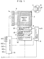
- Fig. 1 is a block diagram of a first novel synchronous burst-access memory.
- Fig. 2 is a timing diagram illustrating the operation of the first novel memory.
- Fig. 3 is a more detailed block diagram of the first novel memory.
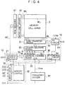
- Fig. 4 is a block diagram of a second novel synchronous burst-access memory.
- Fig. 5 is a timing diagram illustrating the operation of the second novel memory.
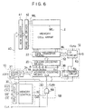
- Fig. 6 is a block diagram of a third novel synchronous burst-access memory.
- Fig. 7 is a timing diagrams illustrating the operation of the third novel memory.
- Fig. 8 is a block diagram of a fourth novel synchronous burst-access memory.
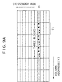
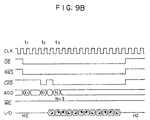
- Fig. 9A illustrates a block addressing scheme.
- Fig. 9B is a timing diagram illustrating burst access to three blocks in Fig. 9A by the fourth novel memory.
- Fig. 10 is a block diagram of a fifth novel synchronous burst-access memory.
- Fig. 11A illustrates two groups of three blocks each in the fifth novel memory.
- Fig. 11B is a timing diagram illustrating burst access to the blocks indicated in Fig. 11A by the fifth novel memory.
- Fig. 12 is a block diagram of a sixth novel synchronous burst-access memory.
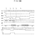
- Fig. 13A illustrates two four-bit blocks in the sixth novel memory.
- Fig. 13B is a timing diagram illustrating burst access to the blocks indicated in Fig. 13A by the fifth novel memory.
- Fig. 14 is a block diagram of a seventh novel synchronous burst-access memory.
- Fig. 15 is a timing diagram illustrating the operation of the seventh novel memory.
- Fig. 16 is a block diagram of an eighth novel synchronous burst-access memory.
- Fig. 17 is a schematic diagram of the flag shifting circuit in Fig. 16.
- Fig. 18 is a timing diagram illustrating the operation of the flag-shifting circuit.
- Fig. 19 is a timing diagram illustrating the operation of the eighth novel synchronous burst-access memory when the SFT signal is high.
- Fig. 20 is a timing diagram illustrating the operation of the eighth novel synchronous burst-access memory when the SFT signal is low.
- Fig. 21 is a block diagram of a novel word-line driving circuit for a synchronous dynamic memory.
- Fig. 22 is a timing diagram illustrating operation of the novel word-line driving circuit.
- a first novel synchronous burst-access memory comprises a memory cell array 2 having memory cells disposed in intersecting rows and columns.
- rows are represented by horizontal word lines 4 and columns by vertical bit lines 6.
- Dynamic random-access memory cells 8 are disposed near the intersections of the bit lines and word lines, as shown in the inset in Fig. 1 for example.
- the memory cell array also comprises sense amplifiers and other well-known devices not explicitly shown in the drawings.
- the novel memory also has a latching means 10, clocked by a clock signal CLK, for receiving and latching a row address strobe signal RAS ⁇ , a column address strobe signal CAS ⁇ , and address signals A 0 , A 1 , A 2 , ..., A k , which are carried on an external address bus ADD.
- the memory must also receive one or more signals for differentiating between read access and write access.
- the latching means 10 receives and latches for this purpose a write enable signal WE ⁇ and an output enable signal OE ⁇ .
- a novel feature of the invention is that RAS ⁇ , CAS ⁇ , WE ⁇ , OE ⁇ , and the address signals A 0 , ..., A k are all latched on rising or falling edges of the clock signal CLK.
- the latching means 10 comprises latch circuits for latching the above-mentioned input signals, and further circuitry for passing the latched input signals to other parts of the burst-access synchronous memory, and for generating various control signals from the latched input signals.
- Transparent latches can be used advantageously, as will be shown later in Figs. 21 and 22.
- the invention is not restricted to the signals shown in Fig. 1.
- WE ⁇ and OE ⁇ may be replaced by a single read/write signal (R/ W ⁇ ).
- R/ W ⁇ read/write signal
- An input/output means 12 also clocked by the clock signal CLK, is connected to and controlled by the latching means 10.
- the input/output means has a data I/O port (marked I/O in the drawings) via which data are input to and output from the memory in serial fashion, synchronized with CLK. When not used for data input or output, the I/O port is placed in the high-impedance state.
- the I/O port may comprises a single signal line as shown in the drawing, in which case only one data bit is input or output at a time.
- the I/O port may comprise more than one signal line, in which case two or more data bits are input or output simultaneously.
- the number of bit lines (actually bit line pairs) per column in the memory cell array equals the number of data lines in the I/O port.
- a row address decoding means 14 connected to the memory cell array 2 and the latching means 10 receives the latched address signals A 0 , ..., A k and a first internal control signal from the latching means 10, decodes the address information, thereby selects one of the word lines 4, and drives this word line, thus selecting a row of memory cells in the memory cell array 2.
- the first internal control signal which controls the time at which these operations are carried out, is generated from the row address strobe signal RAS ⁇ and the clock signal CLK. Alternatively, RAS ⁇ and CLK may be passed directly to the address decoding means 14 as the first internal control signal.
- An address counting means 18 is connected to and controlled by the latching means 10 and receives the clock signal CLK. By counting CLK pulses, the address counting means 18 generates a consecutive series of column addresses (A) starting from a preset address as will be described later. Each address A comprises m address bits A 0 , A 1 , A 2 , ..., A m . The address counting means 18 thus operates as a presettable (m + 1)-bit counter. The number of address bits A 0 , ..., A m generated is equal to or greater than the number of address bits A 0 , ..., A k latched by the latching means 10.
- a column address decoding means 20 connected to the address counting means 18 decodes the column addresses output by the address counting means 18 and selects corresponding columns in the memory cell array 2, selecting one column at a time.
- the data are transferred to and from only those memory cells 8 disposed in the column selected by the column address decoding means 20, in the row selected by the row address decoding means 14. Data are thus transferred to or from a consecutive series of column positions in the row, one column position at a time.
- Fig. 2 illustrates a burst read access.
- an external device such as a processor begins by driving RAS ⁇ low (active) and sending a row address Xa on the address bus ADD.
- the latching means 10 latches RAS ⁇ and the row address Xa.
- the row address decoding means 14 decodes Xa and selects one of the word lines 4 in the memory cell array 2.
- the processor drives CAS ⁇ and OE ⁇ low (active) and sends a column address Ya on the address bus ADD.
- the latching means 10 latches CAS ⁇ and OE ⁇ and sets the value of Ya in the address counting means 18.
- the column address Ya may be latched in the latching means 10, using a latch separate from the latch that holds the row address Xa.
- the column address Ya may be passed directly through the latching means 10 to the address counting means 18.
- the column address Ya is passed to the address counting means 18 together with a second internal control signal commanding the address counting means 18 to preset to the value Ya.
- the second internal control signal can be generated from CAS ⁇ and CLK: for example, from the first rising edge of CLK after CAS ⁇ goes low.
- the column address Ya is set in the k + 1 most significant bits of the m + 1 bits of the address counting means 18, and the other bits are cleared to zero. From CAS ⁇ and OE ⁇ the latching means 10 also generates and sends to the input/output means 12 a signal commanding the input/output means 12 to commence output operations.
- the column address decoding means 20 decodes the column address A 0 , ..., A m output by the address counting means 18, thereby selecting one column in the memory cell array.
- the data transfer means 22 transfers the data D 1 in the memory cell or cells at the intersection of this column and the row selected by the row address decoding means 14 to the input/output means 12 for output at the I/O port.
- the processor can latch the data D 1 at time t 2 .
- the address counting means 18 now increments by one, selecting the next column, and the data D 2 in this column in the selected row are output in the same way at time t 3 . Operation continues in this way at times t 4 , t 5 , ..., t n . At each CLK cycle the address counting means 18 increments by one and a new column of data in the same row is output.
- the processor After receiving data n - 1 times, the processor drives CAS ⁇ high (inactive) again. At time t n+1 the latching means 10 latches the inactive CAS ⁇ signal and sends the input/output means 12 an internal control signal commanding it discontinue output operations. When the last data D n has been output, the input/output means 12 places the I/O port in the high-impedance state, denoted HZ in the drawings. The processor then drives RAS ⁇ and OE ⁇ high (inactive) to end the burst access.
- the processor follows a similar procedure except that it leaves OE ⁇ high and drives WE ⁇ low, causing the input/output means 12 to perform input instead of output.
- Data provided by the processor in synchronization with the clock signal CLK are transferred from the I/O port via the data transfer means 22 to successive columns of memory cells in the selected row in the memory cell array 2.
- each of the data D 1 , ..., D n consists of a single bit. If the I/O port consists of multiple signal lines, then each of the data D 1 , ..., D n consists of multiple bits.
- the data transfer means 22 comprises only gating means for connecting bit lines 6 in the selected column to the input/output means 12. If necessary, however, the data transfer means 22 may have a data register as in conventional dual-port RAM. In this case an entire row of data is transferred from the selected word line to the data transfer means 22 at the beginning of the burst access, between times t 0 and t 1 in Fig. 2, and stored in the data register. The data in the data register are then written or read at times t 1 to t n+1 . For write access, after time t n+1 the entire row of data is transferred back from the data transfer means 22 to the selected row in the memory cell array 2.
- address signals (A 0 , ..., A k ) and control signals ( RAS ⁇ , CAS ⁇ , WE ⁇ , OE ⁇ ) are sent to the memory only once per burst, access takes place much more rapidly than with conventional dynamic RAM, new data being obtained in every clock cycle. Since the novel memory has only one port, it is smaller, simpler, and less expensive to manufacture and test than conventional dual-port RAM. It is also simpler to control.
- the novel memory does not enable random and serial access to be performed simultaneously.
- Many personal computer systems and other systems that employ dual-port RAM do not need to access the two ports simultaneously, however. Such systems will obtain significant cost benefits from using the novel memory.
- Fig. 3 is a somewhat more detailed block diagram of the first novel memory. Fig. 3 is shown mainly to relate the foregoing description to the descriptions of subsequent novel memories, in which further elements will be added.
- the latching means 10 is shown to comprise an input latch circuit 30 for latching RAS ⁇ , CAS ⁇ , WE ⁇ , and OE ⁇ , and an address buffer 31 connected to the external address bus ADD for latching address signals.
- a memory control signal generating circuit 32 connected to the output side of the input latch circuit 30 generates internal control signals, and controls the address buffer 31 so that row addresses are sent to the row address decoding means 14 and column addresses to the address counting means 18. Control signals from the memory control signal generating circuit 32 are conveyed to the address buffer 31, the address counting means 22, and the input/output means 12 via several signal lines which are shown for convenience in the drawings as a single signal line 33.
- the output side of the address buffer 31 is connected via an internal column address bus 34 to the address counting means 18, and via an internal row address bus 35 to the row address decoding means 14.
- the row address decoding means 14 comprises a row address decoder 41 and a word-line driver 42.
- the row address decoder 41 decodes the row address received from the address buffer and selects one of the word lines, such as WL i in the drawing.
- the word-line driver 42 drives the selected word line WL i .
- the input/output means 12 comprises an input/output control circuit 36 and an input/output circuit 53, both of which receive the clock signal CLK.
- the input/output circuit 53 is connected to the data transfer means 22 via an internal data bus 52 comprising one or more data lines, which are connected via well-known buffer circuits not explicitly shown in the input/output circuit 53 to the equal number of data lines in the I/O port.
- the input/output control circuit 36 receives control signals from the memory control signal generating circuit 32 via the signal line 33, and sends further control signals to the input/output circuit 53 via a signal line 54. These further control signals place the input/output circuit 53 in the input state, the output state, or a high-impedance state in which neither input nor output is performed.
- Fig. 4 is a block diagram of a second novel synchronous burst-access memory. Elements identical to elements in Fig. 3 are identified by the same reference numerals.
- the second novel memory differs from the first novel memory in having a frequency divider 57 that receives the clock signal CLK, divides its frequency by a factor N (where N is a positive integer), thus generates an internal clock signal CLKa, and supplies CLKa in place of CLK to the input latch circuit 30, the address buffer 31, the address counting means 18, the input/output control circuit 36, and the input/output circuit 53.
- Frequency dividing circuits are well known, so a detailed description will be omitted.
- the frequency division ratio N can be selected by one or more external control signals not shown in the drawing. Alternatively, N can be permanently selected when the memory is fabricated, by a manufacturing option such as a metalization mask option, laser trimming option, or wire bonding option.
- CLK is shown as having twice the frequency of the CLK signal in Fig. 2.
- CLKa signal obtained by dividing the frequency of CLK by two accordingly has the same frequency in Fig. 5 as CLK in Fig. 2.
- the burst access shown in Fig. 5 is identical to that in Fig. 2 except that CLK is replaced by CLKa.
- the frequency divider 57 enables the novel memory in Fig. 4 to be easily adapted for use with processors having different access speeds. Users will benefit by not having to provide a separate clock-dividing circuit. Manufacturers will benefit by being able to offer a single memory device suitable for a wide range of applications.
- the second novel memory can be used in a system having two or more processors that access memory at different speeds. When accessing the memory, each processor selects the appropriate value of N by driving the external control signal or signals to the appropriate levels.
- Fig. 6 is a block diagram of a third novel synchronous burst-access memory. Elements identical to elements in Fig. 3 are identified by the same reference numerals.
- the third novel memory has, in addition to the circuit elements shown in Fig. 3, a clock control circuit 58 for blocking input of the clock signal CLK to the address counting means 18 and the input/output means while CAS ⁇ is high.
- the clock control circuit comprises, for example, a two-input OR gate 59: one input receives CLK; the other receives CAS ⁇ from the memory control signal generating circuit 32.
- the output CLKb of the OR gate 59 is thus high whenever CAS ⁇ is high, and is identical to CLK when CAS ⁇ is low.
- CLKb is supplied to the address counting means 18, the input/output control circuit 36, and the input/output circuit 53 in place of CLK.
- Fig. 7 illustrates a burst read access for the third novel memory.
- CAS ⁇ is initially held low for substantially three CLK cycles, causing the clock control circuit 58 to generate three CLKb pulses.
- Data D 1 , D 2 , and D 3 are output and the address counting means 18 increments three times.
- Next CAS ⁇ is held high for substantially four CLK cycles, causing CLKb to remain high for a similar interval.
- the address counting means 18 does not increment, and a third internal control signal generated by the memory control signal generating circuit 32 causes the input/output control circuit 36 to place the input/output circuit 53 in the high-impedance state.
- RAS ⁇ remains low; the same word line remains selected in the memory cell array 2.
- Write access is similar to read access except that WE ⁇ is driven low instead of OE ⁇ .
- the third novel memory is particularly useful in systems in which the same data bus is shared by two or more processors or other bus-master devices. While a first processor is engaged in a long burst access, a second processor may obtain use of the bus by asking the first processor to release the bus temporarily. The first processor does so by driving CAS ⁇ high. When the second processor has finished using the bus, the first processor continues its access by driving CAS ⁇ low again without having to generate new address information.
- Fig. 8 is a block diagram of a fourth novel synchronous burst-access memory. Elements identical to elements in Fig. 3 are identified by the same reference numerals.
- the fourth novel memory has an access counting means 60 for counting clock signals and halting input or output when a predetermined number of accesses have been performed.
- the access counting means 60 comprises a down-counter 61 connected to the address buffer 31 via an internal address bus 62, to the memory control signal generating means 32 via the signal line 33, and to the address counting means 18 and the input/output control circuit 36 via a signal line 64.
- the down-counter 61 preferably has the same bit width as the address counting means 18.
- bit width of the external address bus ADD differs from the bit width of the address counting means 18 and the down-counter 61.
- m k + 2.
- Fig. 9A shows the address structure of the memory cell array 2 in the fourth novel memory.
- the I/O port and the internal data bus 51 consist of only a single data line each, so that the memory cell array 2 has one bit per column. This is not a restriction on the invention; the structure can easily be extended to multiple bits per column.
- a given row address X input to the memory designates a single word line, but a (k + 1)-bit column address Y designates four bits (four columns) in that word line, such a group of four bits being referred to herein as a block.
- the four bits in the block corresponding to row address X 1 , column address Y 1 are identified by circles with different quadrant markings, and bits in the two succeeding blocks are similarly identified. Burst access to these twelve bits will be illustrated next.
- Fig. 9B illustrates a burst read access for the fourth novel memory.
- the row address X 1 is latched at time t 1 and the column address Y 1 at time t 2 .
- the address counting means 18 is preset with Y 1 in the most significant k + 1 bits and zero in the two remaining bits. At the same time the down-counter 61 is cleared to zero.
- the address counting means 18 now begins incrementing, generating column addresses that select individual bits in the memory cell array. In the first four clock cycles after t 2 the four bits in block (X 1 , Y 1 ) are selected for access, one after another; in the next four clock cycles the four bits in the block (X 1 , Y 1 + 1) are selected and accessed; then the four bits in the block (X 1 , Y 1 + 2) are selected and accessed.
- the processor drives CAS ⁇ high; then it drives CAS ⁇ low again and places an access count on the external address bus ADD, indicating the number of blocks to be accessed.
- the down-counter 61 has already decremented from zero to, for example, minus two: in binary notation, from (00...00000) B to (11...11110) B .
- the value (10) B in the two least significant bits is left unaltered and the value three, or (00...011) B , is set in the other bits, so the complete value of the down-counter 61 becomes, for example, (00...01110) B or fourteen.
- the down-counter 61 is designed to generate a count-out signal when its count reaches a certain value: for example, the value three, or (00...00011) B , at which the most significant k + 1 bits all become zero. This value should be selected so that it is reached when the requested number of blocks have been accessed.
- the count-out signal (referred to elsewhere as a fourth internal control signal) is sent via the signal line 64 to the address counting means 18 and the input/output control circuit 36 in Fig. 8, causing the address counting means 18 to stop counting and the input/output control circuit 36 to place the I/O port in the high-impedance state. After this, the processor drives CAS ⁇ and other control signals inactive.
- Write access is similar to read access except that WE ⁇ is driven low instead of OE ⁇ .
- the fourth novel memory has the same advantages as the first novel memory, with the following additional advantages.
- the I/O port In read access, the I/O port is placed in the high-impedance state as soon as the necessary number of bits have been accessed, even if the processor does not immediately deactivate CAS ⁇ and other control signals. This feature is useful in a system having a shared data bus, since it enables the data bus to be transferred promptly to another device.
- image-processing operations such as clip and fill can be carried out extremely conveniently.
- the access count can be used to control the number of bits written, thereby masking bits which are to be left unaltered.
- the processor can control the number of bits accessed without having to deactivate CAS ⁇ and other control signals at exact times.
- the block address structure shown in Fig. 9A enables memory capacity to be increased without increasing either the number of external address lines (A 0 , ..., A k ) or the number of data lines in the I/O port, and furthermore enables access to begin even before the access count is received. Similar block structures can be employed in the first, second, and third novel memories.
- the fourth novel memory can easily be adapted to block structures in which all bits in the same block are disposed in the same column and have the same column address A 0 , ..., A m , but are accessed in a serial manner by the input/output means.
- k and m may be equal, the address counting means 18 being, for example, an (m + 3)-bit counter that outputs only the m + 1 most significant bits A 0 , ..., A m , so that the column address changes only once every four clock cycles.
- the inventive concept of the fourth novel memory is also applicable to memories having a non-blocked address structure.
- the start of data input or output may be delayed until the access count has been preset in the down-counter 61.
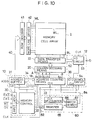
- Fig. 10 is a block diagram of a fifth novel synchronous burst-access memory. Elements identical to elements in Fig. 8 are identified by the same reference numerals.
- the fifth novel memory also has an access counting means 60 for counting accesses and halting input or output when a requested number of accesses have been performed.
- the difference from the fourth novel memory is that the access counting means 60 comprises a register 65, an up-counter 66, and a match detecting circuit 67, instead of the down-counter 63 in the fourth novel memory.
- the register 65 and up-counter 66 have the same bit width as the address counting means 18.
- the register 65 is connected via the internal address bus 62 to the address buffer 31.
- the memory control signal generating circuit 32 commands the address buffer 31 to send the current address value to the address counting means 18.
- the memory control signal generating circuit 32 commands the address buffer 31 to send the current address value to the register 65.
- the address values set the most significant k + 1 bits of the address counting means 18 and the register 65.
- the register 65 stores the value received from the address buffer 31 until it receives a new value from the address buffer 31, and outputs the stored value to the match detecting circuit 67.
- the up-counter 66 counts CLK cycles and outputs the count to the match detecting circuit 67.
- the up-counter 67 is reset to an initial value such as zero by a control signal generated by the memory control signal generating circuit 32 when CAS ⁇ goes low for the first time after RAS ⁇ goes low.
- the match detecting circuit 67 is connected to the address counting means 18 and the input/output control circuit 36 via the signal line 64.
- the match detecting circuit 67 compares the count output by the up-counter 66 with the value received from the register 65. When this count and value match, the match detecting circuit 67 generates an internal control signal on the signal line 64.
- This internal control signal (also referred to as a fourth internal control signal) causes the address counting means 18 to stop counting, and the input/output control circuit 36 to place the input/output circuit 53 in the high-impedance state.
- Figs. 11A and 11B show two twelve-bit burst accesses.
- the first twelve bits to be accessed are located in three consecutive blocks starting at row address X 1 , column address Y 1 .
- the second twelve bits are located in three consecutive blocks starting at row address X 2 , column address Y 2 .
- the processor first drives RAS ⁇ low and sends the row address X 1 , then drives CAS ⁇ low and sends the column address Y 1 .
- the column address Y 1 is passed from the address buffer 31 to the address counting means 18.
- the up-counter 66 is cleared to zero. Output of data now begins as in Fig. 9B, with the up-counter 66 counting the number of bits output.
- the output of the up-counter 66 matches the value stored in the register 65. Detecting this match, the match detecting circuit 67 generates a fourth internal control signal that forthwith halts the address counting means 18 and commands the input/output control circuit 36 to place the input/output circuit 53 in the high-impedance state.
- the processor drives RAS ⁇ and CAS ⁇ high, ending the first access cycle.
- the processor next drives RAS ⁇ low and sends a new row address X 2 , then drives CAS ⁇ low and sends a new column address.
- These new addresses are latched at times t 3 and t 4 , respectively, and output of the data starting at address (X 2 , Y 2 ) begins.
- the memory outputs twelve bits, then halts output and places the input/output circuit 53 in the high-impedance state.
- Write access is similar to read access except that WE ⁇ is driven low instead of OE ⁇ .
- the fifth novel memory provides the same advantages as the fourth, with the further advantage that when a processor performs repeated burst accesses of the same length, it only has to specify the length once.
- a further advantage is that if a processor neglects to specify an access length, because of a programming error for example, this will not in general cause the memory to attempt a burst access of the maximum length, because the previous length will be stored in the register 65 as a default value.
- Fig. 12 is a block diagram of a sixth novel synchronous burst-access memory that combines the features of the third and fourth novel memories. Elements identical to elements in Fig. 8 are identified by the same reference numerals.
- the sixth novel memory like the fourth novel memory, has an access counting means 60 comprising a down-counter 61 for counting accesses and halting input or output when a requested count is reached.
- the address buffer 31 in Fig. 12 is divided into a first buffer 68 and a second buffer 69.
- the first buffer 68 supplies a row address to the row address decoder 41 and a column address to the address counting means 18;
- the second buffer 69 supplies the value on the address bus ADD to the access counting means 60.
- a disabling circuit 70 receives the clock signal CLK, sends control signals to the second buffer 69 and the memory control signal generating circuit 32, and receives a control signal from the memory control signal generating circuit 32.
- the disabling circuit 70 comprises, for example, a simple counter circuit. The function of the disabling circuit 70 is to enable the access counting means 60 to receive the value on the address bus only during a certain interval after CAS ⁇ first becomes active following activation of RAS ⁇ .
- the memory control signal generating circuit 32 notifies the disabling circuit 70.
- the disabling circuit 70 enables the second buffer 69, activates a control signal Pz sent to the memory control signal generating circuit 32, and starts counting CLK cycles.
- the disabling circuit 70 disables the second buffer 69 and deactivates Pz.
- Pz is active high.
- the sixth novel memory has a clock control circuit 58 similar to the one in the third novel memory for blocking clock input to the address counting means 18, the input/output control circuit 36, the input/output circuit 53, and the access counting means 60.
- the control signal sent from the memory control signal generating circuit 32 to the clock control circuit 58 is not CAS ⁇ , however, but a signal that blocks CLK only if CAS ⁇ goes high while Pz is low. This signal can be generated, for example, by an AND gate 71 having CAS ⁇ and the inverse of Pz as inputs.
- the memory cell array in Fig. 12 has the structure shown in Fig. 13A. Access to the two blocks comprising data D 1 to D 8 in Fig. 13A will be illustrated next.
- access begins as in the fourth and fifth novel memories, the row address X 1 being latched at time t 1 and the column address Y 1 being preset in the address counting means 18 at time t 2 .
- the disabling means 70 drives the Pz signal high and starts counting CLK cycles.
- CAS ⁇ goes high for one clock cycle between times t 2 and t 3 , but since Pz is high, CAS ⁇ does not block CLK.
- the address counting means increments normally, and data output begins with D 1 . Data output continues with D 2 and D 3 while CAS ⁇ goes low again.
- the disabling means 70 drives the Pz signal low, permitting CLK to be gated by CAS ⁇ . Accordingly, if CAS ⁇ subsequently goes high, as it does for three clock cycles around time t 4 for example, the address counting means 18 stops incrementing between times t 4 and t 5 . During this interval the access counting means 60 also stops counting, the I/O port is placed in the high-impedance state on command from the memory control signal generating circuit 32, and access pauses.
- Access resumes after time t 5 , this being the first rising edge of CLK after CAS ⁇ goes low again, and the remaining data D 4 , ..., D 8 are output.
- the access counting means 60 terminates the access by stopping the address counting means 18 and causing the I/O port to be placed in the high-impedance state again.
- the sixth novel memory has the advantages of both the third and fourth novel memories: access can be temporarily halted by driving CAS ⁇ high in order to allow another device to use the data bus; the data bus is released promptly when the requested number of bits have been accessed; and in write access, the access count can be used to mask bits in image-processing operations such as clip and fill.
- Fig. 14 is a block diagram of a seventh novel synchronous burst-access memory. Elements identical to elements in Fig. 8 are identified by the same reference numerals.
- This seventh novel memory is similar to the fourth novel memory but has an additional flag output circuit 72 that also receives the signal output by the access clock counting means 60 on the signal line 64 when the requested number of accesses have been performed. On receiving this signal, the flag output circuit 72 asserts an external flag signal denoted FLAG in the drawings to notify external devices that the burst access has ended.
- the flag output circuit comprises, for example, a flip-flop circuit that is set by the signal from the access counting means 60 and reset (via a signal line not shown in the drawing) when RAS ⁇ goes high.
- the operation of the seventh novel memory, illustrated in Fig. 15, is identical to the operation of the fourth novel memory illustrated in Fig. 9B with the addition of the flag output signal which goes high when a burst access is completed.
- the advantage of the seventh novel memory is that a processor can delegate memory access to a memory management unit and execute other operations without having to count accessed bits.
- the flag signal notifies the processor (or other external devices) that the memory is available to begin the next burst access.
- Fig. 16 is a block diagram of an eighth novel synchronous burst-access memory. Elements identical to elements in Fig. 14 are identified by the same reference numerals.
- the access counting means 60 in Fig. 16 is adapted to generate a signal Pend that goes active a certain number of CLK cycles before the requested number of accesses have been completed. If the access counting means comprises a down-counter 61, for example, the Pend signal can be generated when a certain positive count is reached, this count being higher than the count value indicating completion of access.
- the Pend signal is sent to a flag shifting circuit 73 and delayed by a certain time, the length of the delay being controlled, for example, by an externally input shift control signal denoted SFT.
- the delayed signal denoted Pfsft in the drawings, is sent to the flag output circuit 72 and causes output of the flag signal.
- Fig. 17 is a schematic diagram of the flag shifting circuit 73 in Fig. 16, also showing the flag output circuit 72.
- This flag shifting circuit 73 comprises an n-clock delay circuit 80 that receives the Pend and CLK signals and delays Pend by n CLK cycles, a tri-state buffer 81 that inputs Pend, an inverter 82 that inverts SFT, and a tri-state buffer 83 that receives the output of the n-clock delay circuit 80.
- the tri-state buffer 83 is enabled by the SFT signal; the tri-state buffer 81 is enabled by the inverted SFT signal created by the inverter 82. When enabled, both tri-state buffers 81 and 83 act as inverters.
- the output of whichever tri-state buffer 81 or 83 is enabled is inverted again by an inverter 84 to generate the output signal Pfsft which is sent to the flag output circuit 72.
- SFT is low, Pfsft lags Pend by only the slight propagation delay of the tri-state buffer 81 and the inverter 84.
- SFT is high, however, Pfsft lags Pend by substantially one CLK cycle, going high on the falling edge of CLK in the next CLK cycle after Pend goes high.
- Figs. 19 and 20 illustrate the operation of the eighth novel memory when the access clock counter 63 is adapted to drive Pend high during the penultimate access, and the flag shifting circuit of Fig. 17 is used.
- SFT is high, so flag output is delayed and occurs when access is actually completed.
- SFT is low, so flag output occurs one CLK cycle earlier.
- SFT externally input signal
- the clock-frequency-dividing feature of the second novel memory for example, can be added to any of the other novel memories, and the temporary access halting feature of the sixth novel memory can be combined with the flag output feature of the seventh novel memory, or the shifted flag output feature of the eighth novel memory.
- the word-line driving circuit in Fig. 21 receives the clock signal CLK, the row address strobe signal RAS ⁇ , and address signals (A 0 , ..., A k ) from the external address bus ADD.
- a clock generating circuit 100 combines CLK and RAS ⁇ to generate an address latch clock signal Pa that becomes active when CLK and RAS ⁇ are both active, and remains active until RAS ⁇ becomes inactive. Pa and CLK are active high, and RAS ⁇ is active low.
- the clock generating circuit 100 in Fig. 21 comprises, for example, an inverter 101 that receives and inverts RAS ⁇ , an AND gate 102 that ANDs the inverted RAS ⁇ signal from the inverter 101 with the clock signal CLK, and a flip-flop circuit 103 having set and reset input terminals.
- the set terminal (marked S in the drawing) receives the output of the AND gate 102.
- the reset terminal (marked R) receives RAS ⁇ .
- the output of the flip-flop circuit 103 goes high when the S input is high and the R input is low, remains unchanged while the S and R inputs are both low, and goes low when the S input is low and the R input is high. Transitions in the output of the flip-flop circuit 103 are synchronized with the rising edge of the clock signal CLK, which is supplied to a clock input terminal of the flip-flop 103.
- the clock generating circuit 100 need not be structured as shown in Fig. 21. Other circuit configurations can be used instead.
- the word-line driving circuit in Fig. 21 also has a first transparent latch circuit 104 and a second transparent latch circuit 105.
- a transparent latch is a circuit having a data input, a clock input and a data output. While the clock input is inactive (low in the present case), the data output changes according to the data input. When the clock input becomes active (goes high in the present case), the data output latches at its current value and remains unchanged as long as the clock input stays active.
- the first transparent latch circuit 104 receives RAS ⁇ as its data input and CLK as its clock input, and generates a first internal signal Pb as its data output.
- Pb and RAS ⁇ have opposite polarity, Pb going high when RAS ⁇ goes low and vice versa.
- the second transparent latch circuit 105 receives the address signals A 0 , ..., A k as its data input and Pa as its clock input.
- the second transparent latch circuit 105 accordingly comprises a plurality of one-bit latches that are clocked in parallel by Pa.
- the output of the second transparent latch circuit 105 is supplied via an address generating circuit 106 to a word-line decoding circuit 110.
- the address generating circuit 106 transfers the output of the second transparent latch circuit 105 to the word-line decoding circuit 110 as a row address (ADX).
- the word-line decoding circuit 110 decodes the row address ADX, selects one of a plurality of word lines WL 0 to WL n , and generates a second internal signal Pc that becomes active when a word line has been selected.
- the word-line decoding circuit 110 comprises an X-decoder 111 that decodes the row address ADX and provides output signals to a NOR gate 112 and a plurality of AND gates 113 0 , ..., 113 n .
- the output signals W 0 , ..., W n provided to the AND gates 113 0 , ..., 113 n are the decoded address: as a result of decoding, the X-decoder 111 drives just one of the signals W 0 , ..., W n high.
- the signal X provided to the NOR gate 112 is active low and signifies that the decoding operation has been completed; the signal X can be obtained from the signals W 0 , ..., W n by NOR logic, for example.
- the NOR gate 112 performs NOR logic on the signal X and a signal RAS ⁇ a having the same polarity as RAS ⁇ .
- the output of the NOR gate 112 is the second internal signal Pc, which thus goes high when RAS ⁇ is low and the decoded address is valid, indicating that a word line has been selected.
- the word-line decoding circuit 110 need not be structured as shown in Fig. 21. Other circuit configurations are also possible.
- the first internal signal Pb, the second internal signal Pc, and a control signal are supplied to a gating and driving circuit 120.
- the control signal is the address latch clock signal Pa.
- the gating and driving circuit 120 gates the first internal signal Pb according to the second internal signal Pc and the control signal Pa to generate a drive signal Pd, which drives the word-line selected by the word-line decoding circuit 110.
- the gating and driving circuit 120 in Fig. 21 comprises a three-input AND gate 121 and a word-line driver 122.
- the AND gate 121 receives Pa, Pb, and Pc as inputs, carries out a logical AND operation on these inputs, and sends the resulting output to the word-line driver 122.
- the drive signal Pd generated by the the word-line driver 122 has the same polarity as the signal received from the AND gate 121. Pd is supplied to the AND gates 113 0 , ..., 133 n in the word-line decoding circuit 110, and drives the word line WL i for which the corresponding signal W i from the X-decoder 111 is high.
- the gating and driving circuit 120 need not be structured as shown in Fig. 21.
- a control signal other than Pa can be used as the third input to the AND gate 121, or the output of the AND gate 121 can be used directly as the drive signal Pd, eliminating the word-line driver 122.
- the address latch clock signal Pa, the first and second internal signals Pb and Pc, and the drive signal Pd are all inactive (low).
- No word line is driven: WL 0 , ..., WL n are all low.
- the outputs W 0 , ..., W n of the X-decoder 111 are in an invalid state.
- RAS ⁇ is driven low and a valid row address is placed on the address bus ADD.
- RAS ⁇ and ADD must satisfy setup times Trs and Tas with respect to the rising edge of CLK. Trs and Tas must be long enough for row address decoding to be completed and the first and second internal signals Pb and Pc to become active before the rise of CLK at time t 3 .
- RAS ⁇ goes low and ADD becomes valid before the preceding falling edge of CLK, but this is not a necessary condition.
- RAS ⁇ and ADD input can be synchronized with the falling edge of CLK, as shown in earlier timing diagrams such as Fig. 2.
- the X-decoder finishes decoding the row address and drives just one of the signals W 0 , ..., W n to the high state.
- W 2 is driven high.
- the second internal signal Pc also goes high, signifying that row address decoding and word-line selection have been completed.
- the word-line decoding device is now ready to drive the selected word line as soon as CLK rises.
- word-line driving is synchronized with the rising edge of CLK in Fig. 22, it can of course be synchronized with the falling edge by using transparent latches that close when CLK is low, and making other obvious modifications to the circuits in Fig. 21.
Applications Claiming Priority (4)
| Application Number | Priority Date | Filing Date | Title |
|---|---|---|---|
| JP2196877A JPH0489687A (ja) | 1990-07-25 | 1990-07-25 | 同期式バーストアクセスメモリ |
| JP196877/90 | 1990-07-25 | ||
| JP259697/90 | 1990-09-28 | ||
| JP2259697A JP2878815B2 (ja) | 1990-09-28 | 1990-09-28 | 同期式ダイナミックramのワードラインドライブ装置 |
Publications (3)
| Publication Number | Publication Date |
|---|---|
| EP0468480A2 EP0468480A2 (en) | 1992-01-29 |
| EP0468480A3 EP0468480A3 (en) | 1992-12-30 |
| EP0468480B1 true EP0468480B1 (en) | 1997-01-02 |
Family
ID=26510040
Family Applications (1)
| Application Number | Title | Priority Date | Filing Date |
|---|---|---|---|
| EP91112424A Expired - Lifetime EP0468480B1 (en) | 1990-07-25 | 1991-07-24 | Synchronous burst-access memory and word-line driving circuit therefor |
Country Status (4)
| Country | Link |
|---|---|
| US (3) | US5268865A (ko) |
| EP (1) | EP0468480B1 (ko) |
| KR (1) | KR100214435B1 (ko) |
| DE (1) | DE69123890T2 (ko) |
Cited By (23)
| Publication number | Priority date | Publication date | Assignee | Title |
|---|---|---|---|---|
| US5603012A (en) | 1992-06-30 | 1997-02-11 | Discovision Associates | Start code detector |
| US5625571A (en) | 1994-03-24 | 1997-04-29 | Discovision Associates | Prediction filter |
| US5703793A (en) | 1994-07-29 | 1997-12-30 | Discovision Associates | Video decompression |
| US5761741A (en) | 1994-03-24 | 1998-06-02 | Discovision Associates | Technique for addressing a partial word and concurrently providing a substitution field |
| US5768561A (en) | 1992-06-30 | 1998-06-16 | Discovision Associates | Tokens-based adaptive video processing arrangement |
| US5805914A (en) | 1993-06-24 | 1998-09-08 | Discovision Associates | Data pipeline system and data encoding method |
| US5809270A (en) | 1992-06-30 | 1998-09-15 | Discovision Associates | Inverse quantizer |
| US5835740A (en) | 1992-06-30 | 1998-11-10 | Discovision Associates | Data pipeline system and data encoding method |
| US5907692A (en) | 1992-06-30 | 1999-05-25 | Discovision Associates | Data pipeline system and data encoding method |
| US5956741A (en) | 1994-03-24 | 1999-09-21 | Discovision Associates | Interface for connecting a bus to a random access memory using a swing buffer and a buffer manager |
| US6018354A (en) | 1994-03-24 | 2000-01-25 | Discovision Associates | Method for accessing banks of DRAM |
| US6018776A (en) | 1992-06-30 | 2000-01-25 | Discovision Associates | System for microprogrammable state machine in video parser clearing and resetting processing stages responsive to flush token generating by token generator responsive to received data |
| US6034674A (en) | 1992-06-30 | 2000-03-07 | Discovision Associates | Buffer manager |
| US6067417A (en) | 1992-06-30 | 2000-05-23 | Discovision Associates | Picture start token |
| US6079009A (en) | 1992-06-30 | 2000-06-20 | Discovision Associates | Coding standard token in a system compromising a plurality of pipeline stages |
| US6112017A (en) | 1992-06-30 | 2000-08-29 | Discovision Associates | Pipeline processing machine having a plurality of reconfigurable processing stages interconnected by a two-wire interface bus |
| US6326999B1 (en) | 1994-08-23 | 2001-12-04 | Discovision Associates | Data rate conversion |
| US6330665B1 (en) | 1992-06-30 | 2001-12-11 | Discovision Associates | Video parser |
| US6381180B1 (en) | 1994-12-23 | 2002-04-30 | Micron Technology, Inc. | Distributed write data drivers for burst access memories |
| US6525971B2 (en) | 1995-06-30 | 2003-02-25 | Micron Technology, Inc. | Distributed write data drivers for burst access memories |
| US6601156B2 (en) | 1996-07-03 | 2003-07-29 | Micron Technology, Inc. | Continuous interleave burst access |
| US6615325B2 (en) | 1996-01-11 | 2003-09-02 | Micron Technology, Inc. | Method for switching between modes of operation |
| US7646654B2 (en) | 1994-12-23 | 2010-01-12 | Micron Technology, Inc. | Distributed write data drivers for burst access memories |
Families Citing this family (97)
| Publication number | Priority date | Publication date | Assignee | Title |
|---|---|---|---|---|
| US6249481B1 (en) | 1991-10-15 | 2001-06-19 | Kabushiki Kaisha Toshiba | Semiconductor memory device |
| JP2740063B2 (ja) * | 1990-10-15 | 1998-04-15 | 株式会社東芝 | 半導体記憶装置 |
| US6223264B1 (en) | 1991-10-24 | 2001-04-24 | Texas Instruments Incorporated | Synchronous dynamic random access memory and data processing system using an address select signal |
| US5448714A (en) * | 1992-01-02 | 1995-09-05 | Integrated Device Technology, Inc. | Sequential-access and random-access dual-port memory buffer |
| US6310821B1 (en) | 1998-07-10 | 2001-10-30 | Kabushiki Kaisha Toshiba | Clock-synchronous semiconductor memory device and access method thereof |
| DE69325119T2 (de) * | 1992-03-19 | 1999-11-04 | Toshiba Kawasaki Kk | Taktsynchronisierter Halbleiterspeicheranordnung und Zugriffsverfahren |
| JP2740097B2 (ja) * | 1992-03-19 | 1998-04-15 | 株式会社東芝 | クロック同期型半導体記憶装置およびそのアクセス方法 |
| US6417859B1 (en) | 1992-06-30 | 2002-07-09 | Discovision Associates | Method and apparatus for displaying video data |
| GB2287808B (en) * | 1994-03-24 | 1998-08-05 | Discovision Ass | Method and apparatus for interfacing with ram |
| DE69316955T2 (de) | 1992-09-18 | 1998-07-30 | Hitachi Ltd | Rechenanlage mit synchronem, dynamischem Speicher |
| JPH06202933A (ja) * | 1992-12-28 | 1994-07-22 | Toshiba Corp | 同期式大規模集積回路記憶装置 |
| CA2118662C (en) * | 1993-03-22 | 1999-07-13 | Paul A. Santeler | Memory controller having all dram address and control signals provided synchronously from a single device |
| JPH06290582A (ja) * | 1993-04-02 | 1994-10-18 | Nec Corp | 半導体記憶装置 |
| US5392239A (en) * | 1993-05-06 | 1995-02-21 | S3, Incorporated | Burst-mode DRAM |
| JP2697568B2 (ja) * | 1993-08-26 | 1998-01-14 | 日本電気株式会社 | 半導体記憶装置 |
| US5594699A (en) * | 1993-09-20 | 1997-01-14 | Fujitsu Limited | DRAM with reduced electric power consumption |
| JP3099931B2 (ja) | 1993-09-29 | 2000-10-16 | 株式会社東芝 | 半導体装置 |
| KR100309800B1 (ko) * | 1993-11-08 | 2001-12-15 | 윤종용 | 동기랜덤액세스메모리장치 |
| JP3415664B2 (ja) * | 1993-12-28 | 2003-06-09 | 三菱電機株式会社 | 半導体記憶装置 |
| JP3490131B2 (ja) * | 1994-01-21 | 2004-01-26 | 株式会社ルネサステクノロジ | データ転送制御方法、データプロセッサ及びデータ処理システム |
| KR0122099B1 (ko) * | 1994-03-03 | 1997-11-26 | 김광호 | 라이트레이턴시제어기능을 가진 동기식 반도체메모리장치 |
| DE69533630T2 (de) * | 1994-03-24 | 2005-02-24 | Discovision Associates, Irvine | Verfahren und Vorrichtung zur Schnittstellenbildung mit RAM-Speicher |
| US5696917A (en) * | 1994-06-03 | 1997-12-09 | Intel Corporation | Method and apparatus for performing burst read operations in an asynchronous nonvolatile memory |
| JP2982618B2 (ja) * | 1994-06-28 | 1999-11-29 | 日本電気株式会社 | メモリ選択回路 |
| US5923829A (en) | 1994-08-25 | 1999-07-13 | Ricoh Company, Ltd. | Memory system, memory control system and image processing system |
| US5513148A (en) * | 1994-12-01 | 1996-04-30 | Micron Technology Inc. | Synchronous NAND DRAM architecture |
| US6804760B2 (en) | 1994-12-23 | 2004-10-12 | Micron Technology, Inc. | Method for determining a type of memory present in a system |
| US5675549A (en) * | 1994-12-23 | 1997-10-07 | Micron Technology, Inc. | Burst EDO memory device address counter |
| US5682354A (en) * | 1995-11-06 | 1997-10-28 | Micron Technology, Inc. | CAS recognition in burst extended data out DRAM |
| US5640364A (en) * | 1994-12-23 | 1997-06-17 | Micron Technology, Inc. | Self-enabling pulse trapping circuit |
| US5729503A (en) * | 1994-12-23 | 1998-03-17 | Micron Technology, Inc. | Address transition detection on a synchronous design |
| US5652724A (en) * | 1994-12-23 | 1997-07-29 | Micron Technology, Inc. | Burst EDO memory device having pipelined output buffer |
| US5668773A (en) * | 1994-12-23 | 1997-09-16 | Micron Technology, Inc. | Synchronous burst extended data out DRAM |
| US5598376A (en) * | 1994-12-23 | 1997-01-28 | Micron Technology, Inc. | Distributed write data drivers for burst access memories |
| US5721859A (en) * | 1994-12-23 | 1998-02-24 | Micron Technology, Inc. | Counter control circuit in a burst memory |
| KR0140481B1 (ko) * | 1994-12-31 | 1998-07-01 | 김주용 | 동기식 메모리장치의 데이타신호 분배회로 |
| JPH08195077A (ja) * | 1995-01-17 | 1996-07-30 | Internatl Business Mach Corp <Ibm> | Dramの転送方式 |
| KR100477494B1 (ko) | 1995-01-31 | 2005-03-23 | 가부시끼가이샤 히다치 세이사꾸쇼 | 반도체 메모리 장치 |
| US5717654A (en) * | 1995-02-10 | 1998-02-10 | Micron Technology, Inc. | Burst EDO memory device with maximized write cycle timing |
| KR0156969B1 (ko) * | 1995-05-15 | 1998-12-01 | 김주용 | 버스트 페이지 억세스 장치 |
| US5850368A (en) * | 1995-06-01 | 1998-12-15 | Micron Technology, Inc. | Burst EDO memory address counter |
| KR0171942B1 (ko) * | 1995-06-30 | 1999-03-30 | 김주용 | 버스트 길이 검출 회로 |
| US5625790A (en) * | 1995-09-14 | 1997-04-29 | Micron Technology, Inc. | Method and apparatus for reducing the access time of a memory device by decoding a row address during a precharge period of the memory device |
| US6470405B2 (en) | 1995-10-19 | 2002-10-22 | Rambus Inc. | Protocol for communication with dynamic memory |
| US6810449B1 (en) | 1995-10-19 | 2004-10-26 | Rambus, Inc. | Protocol for communication with dynamic memory |
| US6035369A (en) | 1995-10-19 | 2000-03-07 | Rambus Inc. | Method and apparatus for providing a memory with write enable information |
| KR0170905B1 (ko) * | 1995-11-06 | 1999-03-30 | 김주용 | 디램 |
| US5617555A (en) * | 1995-11-30 | 1997-04-01 | Alliance Semiconductor Corporation | Burst random access memory employing sequenced banks of local tri-state drivers |
| US5729504A (en) * | 1995-12-14 | 1998-03-17 | Micron Technology, Inc. | Continuous burst edo memory device |
| US5966724A (en) * | 1996-01-11 | 1999-10-12 | Micron Technology, Inc. | Synchronous memory device with dual page and burst mode operations |
| JP2970513B2 (ja) * | 1996-01-30 | 1999-11-02 | 日本電気株式会社 | 半導体記憶装置およびその制御方法 |
| JP3768608B2 (ja) * | 1996-01-30 | 2006-04-19 | 株式会社日立製作所 | 半導体装置および半導体記憶装置 |
| US6243768B1 (en) | 1996-02-09 | 2001-06-05 | Intel Corporation | Method and apparatus for controlling data transfer between a synchronous DRAM-type memory and a system bus |
| US5926828A (en) * | 1996-02-09 | 1999-07-20 | Intel Corporation | Method and apparatus for controlling data transfer between a synchronous DRAM-type memory and a system bus |
| KR100218734B1 (ko) * | 1996-05-06 | 1999-09-01 | 김영환 | 싱크로노스 메모리의 내부펄스 신호발생 방법 및 그장치 |
| US6209071B1 (en) * | 1996-05-07 | 2001-03-27 | Rambus Inc. | Asynchronous request/synchronous data dynamic random access memory |
| US5680365A (en) * | 1996-05-16 | 1997-10-21 | Mitsubishi Semiconductor America, Inc. | Shared dram I/O databus for high speed operation |
| US6981126B1 (en) | 1996-07-03 | 2005-12-27 | Micron Technology, Inc. | Continuous interleave burst access |
| JPH10208470A (ja) * | 1997-01-17 | 1998-08-07 | Nec Corp | 同期型半導体記憶装置 |
| US6230245B1 (en) | 1997-02-11 | 2001-05-08 | Micron Technology, Inc. | Method and apparatus for generating a variable sequence of memory device command signals |
| US6175894B1 (en) | 1997-03-05 | 2001-01-16 | Micron Technology, Inc. | Memory device command buffer apparatus and method and memory devices and computer systems using same |
| US5870049A (en) * | 1997-04-16 | 1999-02-09 | Mosaid Technologies Incorporated | Current mode digital to analog converter |
| KR100253564B1 (ko) * | 1997-04-25 | 2000-05-01 | 김영환 | 고속 동작용 싱크로노스 디램 |
| US5996043A (en) | 1997-06-13 | 1999-11-30 | Micron Technology, Inc. | Two step memory device command buffer apparatus and method and memory devices and computer systems using same |
| US6484244B1 (en) | 1997-06-17 | 2002-11-19 | Micron Technology, Inc. | Method and system for storing and processing multiple memory commands |
| US6266379B1 (en) | 1997-06-20 | 2001-07-24 | Massachusetts Institute Of Technology | Digital transmitter with equalization |
| KR100257865B1 (ko) * | 1997-09-04 | 2000-06-01 | 윤종용 | 데이터 입/출력 제어 회로를 구비한 동기형 메모리장치 |
| WO1999019874A1 (en) | 1997-10-10 | 1999-04-22 | Rambus Incorporated | Power control system for synchronous memory device |
| WO1999019805A1 (en) | 1997-10-10 | 1999-04-22 | Rambus Incorporated | Method and apparatus for two step memory write operations |
| US6401167B1 (en) * | 1997-10-10 | 2002-06-04 | Rambus Incorporated | High performance cost optimized memory |
| US6965974B1 (en) * | 1997-11-14 | 2005-11-15 | Agere Systems Inc. | Dynamic partitioning of memory banks among multiple agents |
| US7103742B1 (en) | 1997-12-03 | 2006-09-05 | Micron Technology, Inc. | Burst/pipelined edo memory device |
| US6202119B1 (en) | 1997-12-19 | 2001-03-13 | Micron Technology, Inc. | Method and system for processing pipelined memory commands |
| US5978311A (en) | 1998-03-03 | 1999-11-02 | Micron Technology, Inc. | Memory with combined synchronous burst and bus efficient functionality |
| US6175905B1 (en) | 1998-07-30 | 2001-01-16 | Micron Technology, Inc. | Method and system for bypassing pipelines in a pipelined memory command generator |
| US6072746A (en) | 1998-08-14 | 2000-06-06 | International Business Machines Corporation | Self-timed address decoder for register file and compare circuit of a multi-port CAM |
| US6178488B1 (en) | 1998-08-27 | 2001-01-23 | Micron Technology, Inc. | Method and apparatus for processing pipelined memory commands |
| US6219283B1 (en) | 1998-09-03 | 2001-04-17 | Micron Technology, Inc. | Memory device with local write data latches |
| KR100331547B1 (ko) * | 1999-06-01 | 2002-04-06 | 윤종용 | 레지스터의 저장값에 따라 리프레쉬 사이클을 조정하는 리프레쉬 제어 회로 및 이를 구비하는 동적 메모리 장치의 리프레쉬 방법 |
| JP4220621B2 (ja) * | 1999-07-22 | 2009-02-04 | 富士通マイクロエレクトロニクス株式会社 | 半導体集積回路 |
| DE10108820A1 (de) * | 2001-02-23 | 2002-09-12 | Infineon Technologies Ag | Verfahren zum Betrieb eines integrierten Speichers |
| US8391039B2 (en) | 2001-04-24 | 2013-03-05 | Rambus Inc. | Memory module with termination component |
| US6675272B2 (en) * | 2001-04-24 | 2004-01-06 | Rambus Inc. | Method and apparatus for coordinating memory operations among diversely-located memory components |
| US6580660B1 (en) * | 2002-01-30 | 2003-06-17 | Agilent Technologies, Inc. | Circuit and method for synchronizing multiple digital data paths |
| JP4459527B2 (ja) * | 2002-12-18 | 2010-04-28 | パナソニック株式会社 | 半導体記憶装置 |
| KR100564598B1 (ko) * | 2003-12-22 | 2006-03-29 | 삼성전자주식회사 | 동기식 플래쉬 메모리장치 및 이를 동작시키는 방법 |
| KR100612950B1 (ko) * | 2004-04-22 | 2006-08-14 | 주식회사 하이닉스반도체 | 외부클럭을 사용한 디램의 라스타임 제어회로 및 라스타임제어방법 |
| US7301831B2 (en) | 2004-09-15 | 2007-11-27 | Rambus Inc. | Memory systems with variable delays for write data signals |
| US7927948B2 (en) | 2005-07-20 | 2011-04-19 | Micron Technology, Inc. | Devices with nanocrystals and methods of formation |
| KR100650845B1 (ko) * | 2005-12-27 | 2006-11-28 | 주식회사 하이닉스반도체 | 소비 전력을 감소시키는 버퍼 제어 회로와, 이를 포함하는메모리 모듈용 반도체 메모리 장치 및 그 제어 동작 방법 |
| KR100950483B1 (ko) * | 2008-06-27 | 2010-03-31 | 주식회사 하이닉스반도체 | 셋업/홀드 타임 측정 장치 |
| KR101253443B1 (ko) * | 2011-06-09 | 2013-04-11 | 에스케이하이닉스 주식회사 | 반도체 메모리 장치 및 그 동작 방법 |
| US9431079B1 (en) | 2012-12-13 | 2016-08-30 | Gsi Technology, Inc. | Systems and methods of memory and memory operation involving input latching, self-timing and/or other features |
| US9159391B1 (en) | 2012-12-13 | 2015-10-13 | Gsi Technology, Inc. | Systems and methods of double/quad data rate memory involving input latching, self-timing and/or other features |
| WO2016138054A1 (en) | 2015-02-27 | 2016-09-01 | Corning Incorporated | Optical assembly having microlouvers |
| CN112447218A (zh) | 2019-08-29 | 2021-03-05 | 台湾积体电路制造股份有限公司 | 存储器电路和方法 |
| DE102019128331A1 (de) | 2019-08-29 | 2021-03-04 | Taiwan Semiconductor Manufacturing Co., Ltd. | Gemeinsam genutzter decodiererschaltkreis und verfahren |
Family Cites Families (13)
| Publication number | Priority date | Publication date | Assignee | Title |
|---|---|---|---|---|
| US4513372A (en) * | 1982-11-15 | 1985-04-23 | Data General Corporation | Universal memory |
| JPS6072020A (ja) * | 1983-09-29 | 1985-04-24 | Nec Corp | デュアルポ−トメモリ回路 |
| US4608678A (en) * | 1983-12-23 | 1986-08-26 | Advanced Micro Devices, Inc. | Semiconductor memory device for serial scan applications |
| US4984217A (en) * | 1985-01-23 | 1991-01-08 | Hitachi, Ltd. | Semiconductor memory |
| JPS6355797A (ja) * | 1986-08-27 | 1988-03-10 | Fujitsu Ltd | メモリ |
| JPH01130240A (ja) * | 1987-11-16 | 1989-05-23 | Yokogawa Hewlett Packard Ltd | データ列発生装置 |
| JPS63225995A (ja) * | 1987-03-16 | 1988-09-20 | Hitachi Ltd | 半導体記憶装置 |
| JPS63247997A (ja) * | 1987-04-01 | 1988-10-14 | Mitsubishi Electric Corp | 半導体記憶装置 |
| JPS63271679A (ja) * | 1987-04-30 | 1988-11-09 | Toshiba Corp | デ−タ書込み方式 |
| KR970008786B1 (ko) * | 1987-11-02 | 1997-05-29 | 가부시기가이샤 히다찌세이사꾸쇼 | 반도체 집적회로 |
| JPH01146187A (ja) * | 1987-12-02 | 1989-06-08 | Mitsubishi Electric Corp | キヤッシュメモリ内蔵半導体記憶装置 |
| JPH028933A (ja) * | 1988-06-27 | 1990-01-12 | Nec Corp | 半導体メモリ装置 |
| JPH0770212B2 (ja) * | 1988-07-19 | 1995-07-31 | 日本電気株式会社 | 半導体メモリ回路 |
-
1991
- 1991-07-23 KR KR1019910012604A patent/KR100214435B1/ko not_active IP Right Cessation
- 1991-07-24 US US07/735,626 patent/US5268865A/en not_active Ceased
- 1991-07-24 EP EP91112424A patent/EP0468480B1/en not_active Expired - Lifetime
- 1991-07-24 DE DE69123890T patent/DE69123890T2/de not_active Expired - Fee Related
-
1993
- 1993-09-15 US US07/121,504 patent/US5327390A/en not_active Expired - Lifetime
-
1995
- 1995-12-04 US US08/565,958 patent/USRE35723E/en not_active Expired - Lifetime
Cited By (50)
| Publication number | Priority date | Publication date | Assignee | Title |
|---|---|---|---|---|
| US5881301A (en) | 1924-06-30 | 1999-03-09 | Discovision Associates | Inverse modeller |
| US6263422B1 (en) | 1992-06-30 | 2001-07-17 | Discovision Associates | Pipeline processing machine with interactive stages operable in response to tokens and system and methods relating thereto |
| US6018776A (en) | 1992-06-30 | 2000-01-25 | Discovision Associates | System for microprogrammable state machine in video parser clearing and resetting processing stages responsive to flush token generating by token generator responsive to received data |
| US6697930B2 (en) | 1992-06-30 | 2004-02-24 | Discovision Associates | Multistandard video decoder and decompression method for processing encoded bit streams according to respective different standards |
| US6112017A (en) | 1992-06-30 | 2000-08-29 | Discovision Associates | Pipeline processing machine having a plurality of reconfigurable processing stages interconnected by a two-wire interface bus |
| US5768561A (en) | 1992-06-30 | 1998-06-16 | Discovision Associates | Tokens-based adaptive video processing arrangement |
| US6079009A (en) | 1992-06-30 | 2000-06-20 | Discovision Associates | Coding standard token in a system compromising a plurality of pipeline stages |
| US5784631A (en) | 1992-06-30 | 1998-07-21 | Discovision Associates | Huffman decoder |
| US6067417A (en) | 1992-06-30 | 2000-05-23 | Discovision Associates | Picture start token |
| US6330665B1 (en) | 1992-06-30 | 2001-12-11 | Discovision Associates | Video parser |
| US6047112A (en) | 1992-06-30 | 2000-04-04 | Discovision Associates | Technique for initiating processing of a data stream of encoded video information |
| US5809270A (en) | 1992-06-30 | 1998-09-15 | Discovision Associates | Inverse quantizer |
| US6330666B1 (en) | 1992-06-30 | 2001-12-11 | Discovision Associates | Multistandard video decoder and decompression system for processing encoded bit streams including start codes and methods relating thereto |
| US6038380A (en) | 1992-06-30 | 2000-03-14 | Discovision Associates | Data pipeline system and data encoding method |
| US5907692A (en) | 1992-06-30 | 1999-05-25 | Discovision Associates | Data pipeline system and data encoding method |
| US5835740A (en) | 1992-06-30 | 1998-11-10 | Discovision Associates | Data pipeline system and data encoding method |
| US6034674A (en) | 1992-06-30 | 2000-03-07 | Discovision Associates | Buffer manager |
| US6035126A (en) | 1992-06-30 | 2000-03-07 | Discovision Associates | Data pipeline system and data encoding method |
| US6435737B1 (en) | 1992-06-30 | 2002-08-20 | Discovision Associates | Data pipeline system and data encoding method |
| US5828907A (en) | 1992-06-30 | 1998-10-27 | Discovision Associates | Token-based adaptive video processing arrangement |
| US6122726A (en) | 1992-06-30 | 2000-09-19 | Discovision Associates | Data pipeline system and data encoding method |
| US5956519A (en) | 1992-06-30 | 1999-09-21 | Discovision Associates | Picture end token in a system comprising a plurality of pipeline stages |
| US5978592A (en) | 1992-06-30 | 1999-11-02 | Discovision Associates | Video decompression and decoding system utilizing control and data tokens |
| US5603012A (en) | 1992-06-30 | 1997-02-11 | Discovision Associates | Start code detector |
| US6799246B1 (en) | 1993-06-24 | 2004-09-28 | Discovision Associates | Memory interface for reading/writing data from/to a memory |
| US5835792A (en) | 1993-06-24 | 1998-11-10 | Discovision Associates | Token-based adaptive video processing arrangement |
| US5829007A (en) | 1993-06-24 | 1998-10-27 | Discovision Associates | Technique for implementing a swing buffer in a memory array |
| US5805914A (en) | 1993-06-24 | 1998-09-08 | Discovision Associates | Data pipeline system and data encoding method |
| US5768629A (en) | 1993-06-24 | 1998-06-16 | Discovision Associates | Token-based adaptive video processing arrangement |
| US5878273A (en) | 1993-06-24 | 1999-03-02 | Discovision Associates | System for microprogrammable state machine in video parser disabling portion of processing stages responsive to sequence-- end token generating by token generator responsive to received data |
| US5956741A (en) | 1994-03-24 | 1999-09-21 | Discovision Associates | Interface for connecting a bus to a random access memory using a swing buffer and a buffer manager |
| US6018354A (en) | 1994-03-24 | 2000-01-25 | Discovision Associates | Method for accessing banks of DRAM |
| US5761741A (en) | 1994-03-24 | 1998-06-02 | Discovision Associates | Technique for addressing a partial word and concurrently providing a substitution field |
| US5625571A (en) | 1994-03-24 | 1997-04-29 | Discovision Associates | Prediction filter |
| US5984512A (en) | 1994-07-29 | 1999-11-16 | Discovision Associates | Method for storing video information |
| US5798719A (en) | 1994-07-29 | 1998-08-25 | Discovision Associates | Parallel Huffman decoder |
| US5995727A (en) | 1994-07-29 | 1999-11-30 | Discovision Associates | Video decompression |
| US5703793A (en) | 1994-07-29 | 1997-12-30 | Discovision Associates | Video decompression |
| US5821885A (en) | 1994-07-29 | 1998-10-13 | Discovision Associates | Video decompression |
| US5801973A (en) | 1994-07-29 | 1998-09-01 | Discovision Associates | Video decompression |
| US5740460A (en) | 1994-07-29 | 1998-04-14 | Discovision Associates | Arrangement for processing packetized data |
| US6217234B1 (en) | 1994-07-29 | 2001-04-17 | Discovision Associates | Apparatus and method for processing data with an arithmetic unit |
| US6326999B1 (en) | 1994-08-23 | 2001-12-04 | Discovision Associates | Data rate conversion |
| US6381180B1 (en) | 1994-12-23 | 2002-04-30 | Micron Technology, Inc. | Distributed write data drivers for burst access memories |
| US6728142B2 (en) | 1994-12-23 | 2004-04-27 | Micron Technology, Inc. | Distributed write data drivers for burst access memories |
| US7646654B2 (en) | 1994-12-23 | 2010-01-12 | Micron Technology, Inc. | Distributed write data drivers for burst access memories |
| US8107304B2 (en) | 1994-12-23 | 2012-01-31 | Round Rock Research, Llc | Distributed write data drivers for burst access memories |
| US6525971B2 (en) | 1995-06-30 | 2003-02-25 | Micron Technology, Inc. | Distributed write data drivers for burst access memories |
| US6615325B2 (en) | 1996-01-11 | 2003-09-02 | Micron Technology, Inc. | Method for switching between modes of operation |
| US6601156B2 (en) | 1996-07-03 | 2003-07-29 | Micron Technology, Inc. | Continuous interleave burst access |
Also Published As
| Publication number | Publication date |
|---|---|
| DE69123890T2 (de) | 1997-07-31 |
| US5327390A (en) | 1994-07-05 |
| EP0468480A3 (en) | 1992-12-30 |
| KR100214435B1 (ko) | 1999-08-02 |
| USRE35723E (en) | 1998-02-03 |
| KR920003305A (ko) | 1992-02-29 |
| EP0468480A2 (en) | 1992-01-29 |
| US5268865A (en) | 1993-12-07 |
| DE69123890D1 (de) | 1997-02-13 |
Similar Documents
| Publication | Publication Date | Title |
|---|---|---|
| EP0468480B1 (en) | Synchronous burst-access memory and word-line driving circuit therefor | |
| US5386385A (en) | Method and apparatus for preventing invalid operating modes and an application to synchronous memory devices | |
| US5703813A (en) | DRAM having multiple column address strobe operation | |
| US5539696A (en) | Method and apparatus for writing data in a synchronous memory having column independent sections and a method and apparatus for performing write mask operations | |
| US5640364A (en) | Self-enabling pulse trapping circuit | |
| US5966724A (en) | Synchronous memory device with dual page and burst mode operations | |
| US5831931A (en) | Address strobe recognition in a memory device | |
| US5729504A (en) | Continuous burst edo memory device | |
| US5661695A (en) | Burst EDO memory device | |
| US5721859A (en) | Counter control circuit in a burst memory | |
| US5668773A (en) | Synchronous burst extended data out DRAM | |
| US5610864A (en) | Burst EDO memory device with maximized write cycle timing | |
| US5717654A (en) | Burst EDO memory device with maximized write cycle timing | |
| US5675549A (en) | Burst EDO memory device address counter | |
| US5808958A (en) | Random access memory with latency arranged for operating synchronously with a micro processor and a system including a data processor, a synchronous DRAM, a peripheral device, and a system clock | |
| US5521879A (en) | Synchronous dynamic random acess memory | |
| US6202119B1 (en) | Method and system for processing pipelined memory commands | |
| US6175905B1 (en) | Method and system for bypassing pipelines in a pipelined memory command generator | |
| EP1100090B1 (en) | Synchronous LSI memory device | |
| US5291580A (en) | High performance burst read data transfer operation | |
| EP0421627B1 (en) | Memory device | |
| US6166970A (en) | Priority determining apparatus using the least significant bit and CAS latency signal in DDR SDRAM device | |
| KR100284987B1 (ko) | 버스트 edo 메모리 장치 어드레스 카운터 | |
| US6041015A (en) | Semiconductor type memory device having consecutive access to arbitrary memory address | |
| US7103742B1 (en) | Burst/pipelined edo memory device |
Legal Events
| Date | Code | Title | Description |
|---|---|---|---|
| PUAI | Public reference made under article 153(3) epc to a published international application that has entered the european phase |
Free format text: ORIGINAL CODE: 0009012 |
|
| AK | Designated contracting states |
Kind code of ref document: A2 Designated state(s): DE FR GB |
|
| PUAL | Search report despatched |
Free format text: ORIGINAL CODE: 0009013 |
|
| AK | Designated contracting states |
Kind code of ref document: A3 Designated state(s): DE FR GB |
|
| 17P | Request for examination filed |
Effective date: 19930423 |
|
| 17Q | First examination report despatched |
Effective date: 19950811 |
|
| GRAG | Despatch of communication of intention to grant |
Free format text: ORIGINAL CODE: EPIDOS AGRA |
|
| GRAH | Despatch of communication of intention to grant a patent |
Free format text: ORIGINAL CODE: EPIDOS IGRA |
|
| GRAH | Despatch of communication of intention to grant a patent |
Free format text: ORIGINAL CODE: EPIDOS IGRA |
|
| GRAA | (expected) grant |
Free format text: ORIGINAL CODE: 0009210 |
|
| AK | Designated contracting states |
Kind code of ref document: B1 Designated state(s): DE FR GB |
|
| REF | Corresponds to: |
Ref document number: 69123890 Country of ref document: DE Date of ref document: 19970213 |
|
| ET | Fr: translation filed | ||
| PLBE | No opposition filed within time limit |
Free format text: ORIGINAL CODE: 0009261 |
|
| STAA | Information on the status of an ep patent application or granted ep patent |
Free format text: STATUS: NO OPPOSITION FILED WITHIN TIME LIMIT |
|
| 26N | No opposition filed | ||
| REG | Reference to a national code |
Ref country code: GB Ref legal event code: IF02 |
|
| REG | Reference to a national code |
Ref country code: GB Ref legal event code: 732E Free format text: REGISTERED BETWEEN 20090416 AND 20090422 |
|
| REG | Reference to a national code |
Ref country code: FR Ref legal event code: TP |
|
| PGFP | Annual fee paid to national office [announced via postgrant information from national office to epo] |
Ref country code: FR Payment date: 20090710 Year of fee payment: 19 |
|
| PGFP | Annual fee paid to national office [announced via postgrant information from national office to epo] |
Ref country code: GB Payment date: 20090722 Year of fee payment: 19 Ref country code: DE Payment date: 20090716 Year of fee payment: 19 |
|
| GBPC | Gb: european patent ceased through non-payment of renewal fee |
Effective date: 20100724 |
|
| REG | Reference to a national code |
Ref country code: FR Ref legal event code: ST Effective date: 20110331 |
|
| PG25 | Lapsed in a contracting state [announced via postgrant information from national office to epo] |
Ref country code: DE Free format text: LAPSE BECAUSE OF NON-PAYMENT OF DUE FEES Effective date: 20110201 |
|
| REG | Reference to a national code |
Ref country code: DE Ref legal event code: R119 Ref document number: 69123890 Country of ref document: DE Effective date: 20110201 |
|
| PG25 | Lapsed in a contracting state [announced via postgrant information from national office to epo] |
Ref country code: FR Free format text: LAPSE BECAUSE OF NON-PAYMENT OF DUE FEES Effective date: 20100802 |
|
| PG25 | Lapsed in a contracting state [announced via postgrant information from national office to epo] |
Ref country code: GB Free format text: LAPSE BECAUSE OF NON-PAYMENT OF DUE FEES Effective date: 20100724 |