CN101789378B - 用于制造半导体器件的方法 - Google Patents
用于制造半导体器件的方法 Download PDFInfo
- Publication number
- CN101789378B CN101789378B CN2009100028576A CN200910002857A CN101789378B CN 101789378 B CN101789378 B CN 101789378B CN 2009100028576 A CN2009100028576 A CN 2009100028576A CN 200910002857 A CN200910002857 A CN 200910002857A CN 101789378 B CN101789378 B CN 101789378B
- Authority
- CN
- China
- Prior art keywords
- substrate
- thin film
- integrated circuit
- film integrated
- roller
- Prior art date
- Legal status (The legal status is an assumption and is not a legal conclusion. Google has not performed a legal analysis and makes no representation as to the accuracy of the status listed.)
- Expired - Fee Related
Links
Images


Classifications
-
- H—ELECTRICITY
- H01—ELECTRIC ELEMENTS
- H01L—SEMICONDUCTOR DEVICES NOT COVERED BY CLASS H10
- H01L27/00—Devices consisting of a plurality of semiconductor or other solid-state components formed in or on a common substrate
- H01L27/02—Devices consisting of a plurality of semiconductor or other solid-state components formed in or on a common substrate including semiconductor components specially adapted for rectifying, oscillating, amplifying or switching and having at least one potential-jump barrier or surface barrier; including integrated passive circuit elements with at least one potential-jump barrier or surface barrier
- H01L27/12—Devices consisting of a plurality of semiconductor or other solid-state components formed in or on a common substrate including semiconductor components specially adapted for rectifying, oscillating, amplifying or switching and having at least one potential-jump barrier or surface barrier; including integrated passive circuit elements with at least one potential-jump barrier or surface barrier the substrate being other than a semiconductor body, e.g. an insulating body
- H01L27/1214—Devices consisting of a plurality of semiconductor or other solid-state components formed in or on a common substrate including semiconductor components specially adapted for rectifying, oscillating, amplifying or switching and having at least one potential-jump barrier or surface barrier; including integrated passive circuit elements with at least one potential-jump barrier or surface barrier the substrate being other than a semiconductor body, e.g. an insulating body comprising a plurality of TFTs formed on a non-semiconducting substrate, e.g. driving circuits for AMLCDs
- H01L27/1259—Multistep manufacturing methods
- H01L27/1262—Multistep manufacturing methods with a particular formation, treatment or coating of the substrate
- H01L27/1266—Multistep manufacturing methods with a particular formation, treatment or coating of the substrate the substrate on which the devices are formed not being the final device substrate, e.g. using a temporary substrate
-
- H—ELECTRICITY
- H01—ELECTRIC ELEMENTS
- H01L—SEMICONDUCTOR DEVICES NOT COVERED BY CLASS H10
- H01L21/00—Processes or apparatus adapted for the manufacture or treatment of semiconductor or solid state devices or of parts thereof
- H01L21/02—Manufacture or treatment of semiconductor devices or of parts thereof
- H01L21/04—Manufacture or treatment of semiconductor devices or of parts thereof the devices having at least one potential-jump barrier or surface barrier, e.g. PN junction, depletion layer or carrier concentration layer
- H01L21/50—Assembly of semiconductor devices using processes or apparatus not provided for in a single one of the subgroups H01L21/06 - H01L21/326, e.g. sealing of a cap to a base of a container
- H01L21/56—Encapsulations, e.g. encapsulation layers, coatings
-
- B—PERFORMING OPERATIONS; TRANSPORTING
- B32—LAYERED PRODUCTS
- B32B—LAYERED PRODUCTS, i.e. PRODUCTS BUILT-UP OF STRATA OF FLAT OR NON-FLAT, e.g. CELLULAR OR HONEYCOMB, FORM
- B32B37/00—Methods or apparatus for laminating, e.g. by curing or by ultrasonic bonding
- B32B37/14—Methods or apparatus for laminating, e.g. by curing or by ultrasonic bonding characterised by the properties of the layers
- B32B37/16—Methods or apparatus for laminating, e.g. by curing or by ultrasonic bonding characterised by the properties of the layers with all layers existing as coherent layers before laminating
- B32B37/20—Methods or apparatus for laminating, e.g. by curing or by ultrasonic bonding characterised by the properties of the layers with all layers existing as coherent layers before laminating involving the assembly of continuous webs only
-
- B—PERFORMING OPERATIONS; TRANSPORTING
- B42—BOOKBINDING; ALBUMS; FILES; SPECIAL PRINTED MATTER
- B42D—BOOKS; BOOK COVERS; LOOSE LEAVES; PRINTED MATTER CHARACTERISED BY IDENTIFICATION OR SECURITY FEATURES; PRINTED MATTER OF SPECIAL FORMAT OR STYLE NOT OTHERWISE PROVIDED FOR; DEVICES FOR USE THEREWITH AND NOT OTHERWISE PROVIDED FOR; MOVABLE-STRIP WRITING OR READING APPARATUS
- B42D25/00—Information-bearing cards or sheet-like structures characterised by identification or security features; Manufacture thereof
- B42D25/40—Manufacture
- B42D25/45—Associating two or more layers
-
- G—PHYSICS
- G06—COMPUTING; CALCULATING OR COUNTING
- G06K—GRAPHICAL DATA READING; PRESENTATION OF DATA; RECORD CARRIERS; HANDLING RECORD CARRIERS
- G06K19/00—Record carriers for use with machines and with at least a part designed to carry digital markings
- G06K19/06—Record carriers for use with machines and with at least a part designed to carry digital markings characterised by the kind of the digital marking, e.g. shape, nature, code
- G06K19/067—Record carriers with conductive marks, printed circuits or semiconductor circuit elements, e.g. credit or identity cards also with resonating or responding marks without active components
- G06K19/07—Record carriers with conductive marks, printed circuits or semiconductor circuit elements, e.g. credit or identity cards also with resonating or responding marks without active components with integrated circuit chips
- G06K19/077—Constructional details, e.g. mounting of circuits in the carrier
- G06K19/07718—Constructional details, e.g. mounting of circuits in the carrier the record carrier being manufactured in a continuous process, e.g. using endless rolls
-
- G—PHYSICS
- G06—COMPUTING; CALCULATING OR COUNTING
- G06K—GRAPHICAL DATA READING; PRESENTATION OF DATA; RECORD CARRIERS; HANDLING RECORD CARRIERS
- G06K19/00—Record carriers for use with machines and with at least a part designed to carry digital markings
- G06K19/06—Record carriers for use with machines and with at least a part designed to carry digital markings characterised by the kind of the digital marking, e.g. shape, nature, code
- G06K19/067—Record carriers with conductive marks, printed circuits or semiconductor circuit elements, e.g. credit or identity cards also with resonating or responding marks without active components
- G06K19/07—Record carriers with conductive marks, printed circuits or semiconductor circuit elements, e.g. credit or identity cards also with resonating or responding marks without active components with integrated circuit chips
- G06K19/077—Constructional details, e.g. mounting of circuits in the carrier
- G06K19/07749—Constructional details, e.g. mounting of circuits in the carrier the record carrier being capable of non-contact communication, e.g. constructional details of the antenna of a non-contact smart card
- G06K19/0775—Constructional details, e.g. mounting of circuits in the carrier the record carrier being capable of non-contact communication, e.g. constructional details of the antenna of a non-contact smart card arrangements for connecting the integrated circuit to the antenna
-
- H—ELECTRICITY
- H01—ELECTRIC ELEMENTS
- H01L—SEMICONDUCTOR DEVICES NOT COVERED BY CLASS H10
- H01L21/00—Processes or apparatus adapted for the manufacture or treatment of semiconductor or solid state devices or of parts thereof
- H01L21/67—Apparatus specially adapted for handling semiconductor or electric solid state devices during manufacture or treatment thereof; Apparatus specially adapted for handling wafers during manufacture or treatment of semiconductor or electric solid state devices or components ; Apparatus not specifically provided for elsewhere
- H01L21/67005—Apparatus not specifically provided for elsewhere
- H01L21/67011—Apparatus for manufacture or treatment
- H01L21/67126—Apparatus for sealing, encapsulating, glassing, decapsulating or the like
-
- H—ELECTRICITY
- H01—ELECTRIC ELEMENTS
- H01L—SEMICONDUCTOR DEVICES NOT COVERED BY CLASS H10
- H01L21/00—Processes or apparatus adapted for the manufacture or treatment of semiconductor or solid state devices or of parts thereof
- H01L21/67—Apparatus specially adapted for handling semiconductor or electric solid state devices during manufacture or treatment thereof; Apparatus specially adapted for handling wafers during manufacture or treatment of semiconductor or electric solid state devices or components ; Apparatus not specifically provided for elsewhere
- H01L21/67005—Apparatus not specifically provided for elsewhere
- H01L21/67011—Apparatus for manufacture or treatment
- H01L21/67132—Apparatus for placing on an insulating substrate, e.g. tape
-
- H—ELECTRICITY
- H01—ELECTRIC ELEMENTS
- H01L—SEMICONDUCTOR DEVICES NOT COVERED BY CLASS H10
- H01L21/00—Processes or apparatus adapted for the manufacture or treatment of semiconductor or solid state devices or of parts thereof
- H01L21/67—Apparatus specially adapted for handling semiconductor or electric solid state devices during manufacture or treatment thereof; Apparatus specially adapted for handling wafers during manufacture or treatment of semiconductor or electric solid state devices or components ; Apparatus not specifically provided for elsewhere
- H01L21/67005—Apparatus not specifically provided for elsewhere
- H01L21/67011—Apparatus for manufacture or treatment
- H01L21/67144—Apparatus for mounting on conductive members, e.g. leadframes or conductors on insulating substrates
-
- H—ELECTRICITY
- H01—ELECTRIC ELEMENTS
- H01L—SEMICONDUCTOR DEVICES NOT COVERED BY CLASS H10
- H01L21/00—Processes or apparatus adapted for the manufacture or treatment of semiconductor or solid state devices or of parts thereof
- H01L21/67—Apparatus specially adapted for handling semiconductor or electric solid state devices during manufacture or treatment thereof; Apparatus specially adapted for handling wafers during manufacture or treatment of semiconductor or electric solid state devices or components ; Apparatus not specifically provided for elsewhere
- H01L21/683—Apparatus specially adapted for handling semiconductor or electric solid state devices during manufacture or treatment thereof; Apparatus specially adapted for handling wafers during manufacture or treatment of semiconductor or electric solid state devices or components ; Apparatus not specifically provided for elsewhere for supporting or gripping
- H01L21/6835—Apparatus specially adapted for handling semiconductor or electric solid state devices during manufacture or treatment thereof; Apparatus specially adapted for handling wafers during manufacture or treatment of semiconductor or electric solid state devices or components ; Apparatus not specifically provided for elsewhere for supporting or gripping using temporarily an auxiliary support
-
- H—ELECTRICITY
- H01—ELECTRIC ELEMENTS
- H01L—SEMICONDUCTOR DEVICES NOT COVERED BY CLASS H10
- H01L23/00—Details of semiconductor or other solid state devices
- H01L23/28—Encapsulations, e.g. encapsulating layers, coatings, e.g. for protection
-
- H—ELECTRICITY
- H01—ELECTRIC ELEMENTS
- H01L—SEMICONDUCTOR DEVICES NOT COVERED BY CLASS H10
- H01L27/00—Devices consisting of a plurality of semiconductor or other solid-state components formed in or on a common substrate
- H01L27/02—Devices consisting of a plurality of semiconductor or other solid-state components formed in or on a common substrate including semiconductor components specially adapted for rectifying, oscillating, amplifying or switching and having at least one potential-jump barrier or surface barrier; including integrated passive circuit elements with at least one potential-jump barrier or surface barrier
- H01L27/12—Devices consisting of a plurality of semiconductor or other solid-state components formed in or on a common substrate including semiconductor components specially adapted for rectifying, oscillating, amplifying or switching and having at least one potential-jump barrier or surface barrier; including integrated passive circuit elements with at least one potential-jump barrier or surface barrier the substrate being other than a semiconductor body, e.g. an insulating body
- H01L27/1214—Devices consisting of a plurality of semiconductor or other solid-state components formed in or on a common substrate including semiconductor components specially adapted for rectifying, oscillating, amplifying or switching and having at least one potential-jump barrier or surface barrier; including integrated passive circuit elements with at least one potential-jump barrier or surface barrier the substrate being other than a semiconductor body, e.g. an insulating body comprising a plurality of TFTs formed on a non-semiconducting substrate, e.g. driving circuits for AMLCDs
-
- B—PERFORMING OPERATIONS; TRANSPORTING
- B32—LAYERED PRODUCTS
- B32B—LAYERED PRODUCTS, i.e. PRODUCTS BUILT-UP OF STRATA OF FLAT OR NON-FLAT, e.g. CELLULAR OR HONEYCOMB, FORM
- B32B2305/00—Condition, form or state of the layers or laminate
- B32B2305/34—Inserts
- B32B2305/342—Chips
-
- H—ELECTRICITY
- H01—ELECTRIC ELEMENTS
- H01L—SEMICONDUCTOR DEVICES NOT COVERED BY CLASS H10
- H01L2221/00—Processes or apparatus adapted for the manufacture or treatment of semiconductor or solid state devices or of parts thereof covered by H01L21/00
- H01L2221/67—Apparatus for handling semiconductor or electric solid state devices during manufacture or treatment thereof; Apparatus for handling wafers during manufacture or treatment of semiconductor or electric solid state devices or components; Apparatus not specifically provided for elsewhere
- H01L2221/683—Apparatus for handling semiconductor or electric solid state devices during manufacture or treatment thereof; Apparatus for handling wafers during manufacture or treatment of semiconductor or electric solid state devices or components; Apparatus not specifically provided for elsewhere for supporting or gripping
- H01L2221/68304—Apparatus for handling semiconductor or electric solid state devices during manufacture or treatment thereof; Apparatus for handling wafers during manufacture or treatment of semiconductor or electric solid state devices or components; Apparatus not specifically provided for elsewhere for supporting or gripping using temporarily an auxiliary support
- H01L2221/68318—Auxiliary support including means facilitating the separation of a device or wafer from the auxiliary support
-
- H—ELECTRICITY
- H01—ELECTRIC ELEMENTS
- H01L—SEMICONDUCTOR DEVICES NOT COVERED BY CLASS H10
- H01L2221/00—Processes or apparatus adapted for the manufacture or treatment of semiconductor or solid state devices or of parts thereof covered by H01L21/00
- H01L2221/67—Apparatus for handling semiconductor or electric solid state devices during manufacture or treatment thereof; Apparatus for handling wafers during manufacture or treatment of semiconductor or electric solid state devices or components; Apparatus not specifically provided for elsewhere
- H01L2221/683—Apparatus for handling semiconductor or electric solid state devices during manufacture or treatment thereof; Apparatus for handling wafers during manufacture or treatment of semiconductor or electric solid state devices or components; Apparatus not specifically provided for elsewhere for supporting or gripping
- H01L2221/68304—Apparatus for handling semiconductor or electric solid state devices during manufacture or treatment thereof; Apparatus for handling wafers during manufacture or treatment of semiconductor or electric solid state devices or components; Apparatus not specifically provided for elsewhere for supporting or gripping using temporarily an auxiliary support
- H01L2221/68354—Apparatus for handling semiconductor or electric solid state devices during manufacture or treatment thereof; Apparatus for handling wafers during manufacture or treatment of semiconductor or electric solid state devices or components; Apparatus not specifically provided for elsewhere for supporting or gripping using temporarily an auxiliary support used to support diced chips prior to mounting
-
- H—ELECTRICITY
- H01—ELECTRIC ELEMENTS
- H01L—SEMICONDUCTOR DEVICES NOT COVERED BY CLASS H10
- H01L2221/00—Processes or apparatus adapted for the manufacture or treatment of semiconductor or solid state devices or of parts thereof covered by H01L21/00
- H01L2221/67—Apparatus for handling semiconductor or electric solid state devices during manufacture or treatment thereof; Apparatus for handling wafers during manufacture or treatment of semiconductor or electric solid state devices or components; Apparatus not specifically provided for elsewhere
- H01L2221/683—Apparatus for handling semiconductor or electric solid state devices during manufacture or treatment thereof; Apparatus for handling wafers during manufacture or treatment of semiconductor or electric solid state devices or components; Apparatus not specifically provided for elsewhere for supporting or gripping
- H01L2221/68304—Apparatus for handling semiconductor or electric solid state devices during manufacture or treatment thereof; Apparatus for handling wafers during manufacture or treatment of semiconductor or electric solid state devices or components; Apparatus not specifically provided for elsewhere for supporting or gripping using temporarily an auxiliary support
- H01L2221/68363—Apparatus for handling semiconductor or electric solid state devices during manufacture or treatment thereof; Apparatus for handling wafers during manufacture or treatment of semiconductor or electric solid state devices or components; Apparatus not specifically provided for elsewhere for supporting or gripping using temporarily an auxiliary support used in a transfer process involving transfer directly from an origin substrate to a target substrate without use of an intermediate handle substrate
-
- H—ELECTRICITY
- H01—ELECTRIC ELEMENTS
- H01L—SEMICONDUCTOR DEVICES NOT COVERED BY CLASS H10
- H01L2924/00—Indexing scheme for arrangements or methods for connecting or disconnecting semiconductor or solid-state bodies as covered by H01L24/00
- H01L2924/0001—Technical content checked by a classifier
- H01L2924/0002—Not covered by any one of groups H01L24/00, H01L24/00 and H01L2224/00
-
- Y—GENERAL TAGGING OF NEW TECHNOLOGICAL DEVELOPMENTS; GENERAL TAGGING OF CROSS-SECTIONAL TECHNOLOGIES SPANNING OVER SEVERAL SECTIONS OF THE IPC; TECHNICAL SUBJECTS COVERED BY FORMER USPC CROSS-REFERENCE ART COLLECTIONS [XRACs] AND DIGESTS
- Y10—TECHNICAL SUBJECTS COVERED BY FORMER USPC
- Y10T—TECHNICAL SUBJECTS COVERED BY FORMER US CLASSIFICATION
- Y10T156/00—Adhesive bonding and miscellaneous chemical manufacture
- Y10T156/10—Methods of surface bonding and/or assembly therefor
- Y10T156/1089—Methods of surface bonding and/or assembly therefor of discrete laminae to single face of additional lamina
- Y10T156/1092—All laminae planar and face to face
- Y10T156/1093—All laminae planar and face to face with covering of discrete laminae with additional lamina
-
- Y—GENERAL TAGGING OF NEW TECHNOLOGICAL DEVELOPMENTS; GENERAL TAGGING OF CROSS-SECTIONAL TECHNOLOGIES SPANNING OVER SEVERAL SECTIONS OF THE IPC; TECHNICAL SUBJECTS COVERED BY FORMER USPC CROSS-REFERENCE ART COLLECTIONS [XRACs] AND DIGESTS
- Y10—TECHNICAL SUBJECTS COVERED BY FORMER USPC
- Y10T—TECHNICAL SUBJECTS COVERED BY FORMER US CLASSIFICATION
- Y10T156/00—Adhesive bonding and miscellaneous chemical manufacture
- Y10T156/17—Surface bonding means and/or assemblymeans with work feeding or handling means
- Y10T156/1702—For plural parts or plural areas of single part
- Y10T156/1712—Indefinite or running length work
Abstract
本发明的目的在于提高在对薄膜集成电路进行密封过程中的生产效率,并且防止损失和破坏。还有,本发明的另外一个目的在于防止薄膜集成电路在运输过程中遭受损伤,并且使得易于搬运薄膜集成电路。本发明提供了一种层压系统,其中使用辊来供给密封用基底、接收IC芯片、分离以及密封。对大量的薄膜集成电路进行分离、密封和接收操作可以通过旋转所述辊来连续地进行;因此,可以极大地提高生产效率。还有,由于使用了相互对置的辊对,因此可以轻易地所述密封薄膜集成电路。
Description
技术领域
本发明涉及一种对薄膜集成电路进行密封的层压系统。本发明还涉及一种包括大量密封起来的薄膜集成电路的IC片材。本发明还涉及一种由大量密封并且卷绕起来的薄膜集成电路形成的卷材。此外,本发明还涉及一种用于制造其中密封有薄膜集成电路的IC芯片的方法。
背景技术
近年来,一种使用形成于玻璃基底上的薄膜集成电路的IC芯片技术(也被称作IC标签、ID标签、RF(射频)标签、无线标签或者电子标签)得到研发。在这些技术中,需要在制造完毕之后将形成于玻璃基底上的薄膜集成电路与玻璃基底分离开,其中,所述玻璃基底为支撑基底。因此,作为一种用于将已经形成于支撑基底上的薄膜集成电路与支撑基底分离开的技术;例如,存在这样一种技术,其中在薄膜集成电路与支撑基底之间设置一个含有硅的释放层,并且该释放层利用一种含有卤素氟化物的气体去除,由此将所述薄膜集成电路与支撑基底分离开(参考文献1:日本专利公告No.8-254686)。
大量的薄膜集成电路被形成在一块玻璃基底上,并且这些薄膜集成电路在将所述释放层去除的同时被单独地分离下来。但是,在对分离下来的薄膜集成电路进行单独密封的情况下生产效率较低。还有,薄膜集成电路薄而轻,因此难以在没有损伤或者破坏的条件下对薄膜集成电路进行密封。
发明内容
鉴于前述问题,本发明的一个目的在于提高在对薄膜集成电路进行密封过程中的生产效率,并且防止损失和破坏。
还有,如前所述,薄膜集成电路非常易于被破坏,因此即使在密封步骤之后也需要小心地对它们进行搬运,从而使得非常难以在没有损伤和破坏的条件下对它们进行运输。
因此,本发明的另外一个目的在于防止薄膜集成电路在运输过程中遭受损伤,并且使得薄膜集成电路易于搬运。
本发明提供了一种层压系统,其中使用辊来供给密封用基底、接收IC芯片、分离以及密封。对形成于一个基底上的大量薄膜集成电路进行分离、密封和接收操作可以通过旋转所述辊来连续地进行;因此,可以极大地提高生产效率。还有,由于使用了相互对置的辊对,因此可以轻易地密封所述薄膜集成电路。
一种根据本发明的层压系统包括:一个用于传送带有至少一个薄膜集成电路的第一基底的传送装置;一个其上卷绕有第二基底的第一供料辊;一个通过将所述薄膜集成电路的第一表面附着在第二基底上而将所述薄膜集成电路与第一基底分离开的剥离辊;一个其上卷绕有待附着在所述薄膜集成电路的第二表面上的第三基底的第二供料辊;一个将所述薄膜集成电路密封在第二基底与第三基底之间的层压装置;以及一个其上卷绕有密封起来的薄膜集成电路的接收辊,其中所述薄膜集成电路的第一表面与第二表面相对设置。
一种根据本发明的层压系统包括:一个其上卷绕有第二基底的第一供料辊;一个通过将形成于第一基底上的至少一个薄膜集成电路的第一表面附着在第二基底上而将这些薄膜集成电路与第一基底分离开的剥离辊;一个其上卷绕有待附着在所述薄膜集成电路的第二表面上的第三基底的第二供料辊;一个将所述薄膜集成电路密封在第二基底与第三基底之间的层压装置;以及一个其上卷绕有密封起来的薄膜集成电路的接收辊,其中所述薄膜集成电路的第一表面与第二表面相 对设置。
一种根据本发明的层压系统包括:一个用于传送带有至少一个薄膜集成电路的第一基底的传送装置;一个其上卷绕有第二基底的第一供料辊;一个其上卷绕有第三基底的第二供料辊;一个层压装置,通过将所述薄膜集成电路的第一表面附着在第二基底上而将所述薄膜集成电路与第一基底分离开,并且将所述薄膜集成电路密封在第二基底与第三基底之间;以及一个其上卷绕有密封起来的薄膜集成电路的接收辊,其中所述薄膜集成电路的第一表面与第二表面相对设置。
一种根据本发明的层压系统包括:一个表面带有至少一个薄膜集成电路的第一基底;一个其上卷绕有第二基底的第一供料辊;一个固定/移动装置(也被称作第一基底控制装置),用于固定住第一基底从而使得第一基底与第二基底的表面相互对置,并且移动第一基底从而使得所述薄膜集成电路的第一表面附着在第二基底上;一个通过将所述薄膜集成电路的第一表面附着在第二基底上而将所述薄膜集成电路与第一基底分离开的剥离辊;一个其上卷绕有待附着在所述薄膜集成电路的第二表面上的第三基底的第二供料辊;一个将所述薄膜集成电路密封在第二基底与第三基底之间的层压装置;以及一个其上卷绕有密封起来的薄膜集成电路的接收辊,其中所述薄膜集成电路的第一表面与第二表面相对设置。
在具有任一种前述结构的层压结构中,层压装置均包括相互对置的第一辊和第二辊。第一辊和第二辊中的至少一个具有加热装置。所述层压装置通过在所述薄膜集成电路经过相互对置的第一辊与第二辊之间的同时执行压力处理和加热处理中的至少一种,密封所述薄膜集成电路。
还有,第二基底和第三基底包括层压薄膜。第二基底的表面包括粘结表面。第三基底的表面也包括粘结表面。
还有,本发明提供了一种IC片材,包括至少一个密封起来的薄膜集成电路,被制成片材状以易于搬运。一种根据本发明的IC片材 具有大量密封在第二基底与第三基底之间的薄膜集成电路。
此外,本发明提供了一种卷材,包括至少一个密封起来的薄膜集成电路,被卷绕起来以易于搬运。一种根据本发明的卷材包括卷绕起来的大量密封在第二基底与第三基底之间的薄膜集成电路。
对于包括前述结构的IC片材或者卷材来说,所述大量薄膜集成电路均具有一个薄膜晶体管和一个用作天线的导电薄膜。这些薄膜集成电路规则排列。还有,第二基底和第三基底均包括层压薄膜。
一种根据本发明用于制造IC芯片的方法,包括下述步骤:在具有绝缘表面的第一基底上形成一个释放层;在第一基底上形成至少一个薄膜集成电路;在所述薄膜集成电路的边界处形成一个开口,以显露出所述释放层的一部分;将一种含有卤素氟化物的气体或者液体导入所述开口内,来去除所述释放层;将所述薄膜集成电路的第一表面附着在第二基底上,来将所述薄膜集成电路与第一基底分离开;将所述薄膜集成电路的第二表面附着在第三基底上,从而使得所述薄膜集成电路被密封在第二基底与第三基底之间;其中,所述薄膜集成电路的第一表面和第二表面相对设置。
在一种根据本发明的层压系统中,其中一个辊用于供给密封用基底,一个辊用于卷绕薄膜集成电路,多个辊用于分离和密封薄膜集成电路,对大量形成于一个基底上的薄膜集成电路进行分离、密封和接收操作可以连续执行;因此,可以提高生产效率并且可以缩短制造时间。
还有,一种根据本发明的层压系统,其利用相互对置的辊对作为层压装置(也被称作密封装置)来密封薄膜集成电路,可以轻易地密封所述薄膜集成电路。
对于根据本发明的IC片材和卷材来说,由于薄膜集成电路已经被密封起来,因此可以轻易地搬运它们,并且防止了所述薄膜集成电路遭受损失和破坏。还有,可以轻易地运输大量的薄膜集成电路。
附图说明
图1示出了一个根据本发明的层压系统。
图2示出了一个根据本发明的层压系统。
图3示出了一个根据本发明的层压系统。
图4示出了一个根据本发明的层压系统。
图5A和5B示出了一种用于制造IC芯片的方法。
图6A和6B示出了一种用于制造IC芯片的方法。
图7A和7B示出了一种用于制造IC芯片的方法。
图8示出了一种用于制造IC芯片的方法。
图9示出了一个IC芯片。
图10A至10E示出了IC芯片的使用模式。
图11A和11B示出了IC芯片的使用模式。
图12A和12B示出了一个根据本发明的辊。
图13示出了一条根据本发明的IC片材。
附图标记说明
11:传送装置 12:第一基底 13:薄膜集成电路 14:第一供料辊 15:第二供料辊 16:剥离辊 17:层压装置 18:第二基底19:第三基底 20:接收辊 21:辊 22:辊 23:箱子 24:箱子25:辊 26:辊 27:辊 28:切割装置 32:辊 33:固定/移动装置34:传送装置 35:传送装置 36:剥离装置 37:层压装置 100:第一基底 101:释放层 102:释放层 103:释放层 104:绝缘膜105:元件组 108:绝缘膜 109:绝缘膜 110:导电层 111:绝缘膜 112:薄膜集成电路 114:开口 115:开口 116:开口 117:开口 118:薄膜集成电路119:薄膜集成电路 121:第二基底122:第三基底 210:IC芯片 211:电源电路 212:时钟脉冲发生电路 213:数据解调/调制电路 214:控制电路 215:接口电路216:存储器 217:数据总线 218:天线 219:读取器/记录器 294:显示区域 295:读取器/记录器 296:IC芯片 297:物品 305:读 取器/记录器 307:IC芯片 397:物品
具体实施方式
下面将参照附图详细地对本发明的实施方式和实施例进行描述。但是,本技术领域那些熟练人员显然明白,本发明并不局限于下面的描述,而是可以在不脱离本发明的实质和范围的条件下在形式和细节上进行多种变化。因此,本发明并不局限于下面对实施方式和实施例的描述。在说明本发明的过程中,相同的附图标记通常指代相同的组成部件,这些组成部件将在下面给予描述。
实施方式1
本发明提供了一种层压系统,其中使用辊来供给密封用基底、接收IC芯片、分离以及密封。下面将参照附图对这种层压系统的主要模式进行描述。
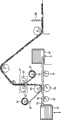
一种根据本发明的层压系统包括:一个用于传送带有大量薄膜集成电路13的第一基底12的传送装置11;一个其上卷绕有第二基底18的第一供料辊14;一个将薄膜集成电路13与第一基底12分离开的剥离辊16;一个其上卷绕有第三基底19的第二供料辊15;一个将薄膜集成电路13密封在第二基底18与第三基底19之间的层压装置17;以及一个其上卷绕有密封起来的薄膜集成电路13的接收辊20(图1)。
在图1所示的设备中,位于由传送装置11传送的第一基底12上的薄膜集成电路13被附着在第二基底18上,以便将薄膜集成电路13与第一基底12分离开,其中第二基底18从第一供料辊14朝向剥离辊16行进。其上附着有薄膜集成电路13的第二基底18沿着层压装置17所在方向行进。第三基底19从第二供料辊15朝向层压装置17行进。在层压装置17处,在薄膜集成电路13附着在第三基底19上的同时执行压力处理和/或加热处理。最后,被密封在第二基底18与 第三基底19之间的薄膜集成电路13沿着接收辊20所在的方向行进,以便卷绕在接收辊20上。
按照前述操作,在根据本发明的层压系统中,剥离辊16、层压装置17以及接收辊20被设置成使得附着在第二基底18和第三基底19上的薄膜集成电路13依次经过它们。剥离辊16和接收辊20沿着相反的方向旋转。第一供料辊14、剥离辊16以及包括于层压装置17中的辊21被设置成使得第二基底18依次经过它们。还有,第一供料辊14、剥离辊16以及辊21沿着相同的方向旋转。第二供料辊15和包括于层压装置17中的辊22被设置成使得第三基底19依次经过它们。第二供料辊15和辊22沿着相同的方向旋转。
传送装置11用于传送带有大量薄膜集成电路13的第一基底12。例如,该传送装置包括一根传送带、大量的辊以及一个机械手。机械手传送第一基底12本身或者传送一个带有第一基底1的台架。传送装置11按照第一供料辊13的旋转速度以一个预定的速度传送第一基底12。
第二基底18被卷绕在第一供料辊14上,而第三基底19被卷绕在第二供料辊15上。通过以预定的速度旋转第一供料辊14而使得第二基底18朝向剥离辊16行进。通过以预定的速度旋转第二供料辊15而使得第三基底19朝向层压装置17行进。第一供料辊14和第二供料辊15均呈圆筒形状,并且由树脂材料、金属材料等等制成。
第二基底18和第三基底19均对应于一个层压薄膜、一张纤维材料纸张等等。层压薄膜可以由一种诸如聚丙烯、聚酯、乙烯基化合物、聚氟乙烯、聚氯乙烯这样的材料制成,并且可以对表面进行处理,例如压纹。
对应于第二基底18和第三基底19的层压薄膜可以由一种诸如聚乙烯和乙烯-醋酸乙烯酯(ethylene vinyl acetate)这样的材料制成。表面可以涂敷二氧化硅(石英)粉末。所述涂层即使在高温高湿氛围中也保持防水。
第二基底18的表面和/或第三基底19的表面可以具有粘结表面。该粘结表面涂敷有一种粘结剂,比如热固性树脂、紫外线固化树脂、环氧基粘结剂或者树脂添加剂。
第二基底18和/或第三基底19可以具有透光性能。还有,第二基底18和/或第三基底19可以在表面上涂敷一种导电材料,以便防止在第二基底18和/或第三基底19中待密封的薄膜集成电路带上静电。
第二基底18和/或第三基底19可以涂敷一种导电材料,比如涂敷含有碳的薄膜作为主要组成部件(金刚石状碳膜)或者涂敷氧化铟锡(ITO)作为防护膜。
剥离辊16用于将薄膜集成电路13的第一表面附着在第二基底18的表面上,以便将薄膜集成电路13与第一基底12分离开。当剥离辊16旋转时,薄膜集成电路13被附着在第二基底18上;由此,薄膜集成电路13与第一基底12分离开。因此,剥离辊16与第一基底12上设置有薄膜集成电路13的侧面对置。
根据前述结构,第一基底12在传送装置11的作用下移动,而剥离辊16固定不动;但是,本发明并不局限于此。第一基底12可以固定不动,而剥离辊16可以移动,从而使得薄膜集成电路13与第一基底12分离开。剥离辊16呈圆筒形状,并且由一种树脂材料、金属材料等等制成。优选的是,剥离辊16由一种柔软材料制成。
当第一表面附着在第二基底18上的薄膜集成电路13抵达层压装置17时,该层压装置17在使得第三基底19附着在薄膜集成电路13的第二表面上的同时,将薄膜集成电路13密封在第二基底18与第三基底19之间。
层压装置17包括相互对置的辊21和辊22。薄膜集成电路13的第二表面被附着在从第二供料辊15朝向辊22行进的第三基底19上,并且在第三基底19经过辊21与辊22之间的同时利用辊21和辊22执行压力处理和/或加热处理。通过前述步骤,薄膜集成电路13被密封在第二基底18与第三基底19之间。
构成层压装置17的辊21和/或辊22包括加热装置。这种加热装置例如对应于一种诸如电热丝或者油这样的加热介质。在不利用辊21和辊22执行加热处理的情况下,辊21和辊22不必具有加热装置。
辊21和辊22按照剥离辊16和第二供料辊15的旋转速度以一个预定的速度旋转。辊21和辊22均呈圆筒形状,并且由一种树脂材料、金属材料等等制成,优选的是由一种柔软材料制成。
接收辊20是一个用于通过卷绕由第二基底18和第三基底19密封起来的薄膜集成电路13来接收这些薄膜集成电路13的辊。接收辊20按照辊21和辊22的旋转速度以一个预定的速度旋转。接收辊20呈圆筒形状,并且由一种树脂材料、金属材料等等制成,优选的是由一种柔软材料制成。
利用根据本发明的系统,第一供料辊14、第二供料辊15、剥离辊16、辊21和22、以及接收辊20发生旋转;由此,可以依次剥离、密封以及接收第一基底12上的大量薄膜集成电路13。因此,根据本发明的系统可以提供较高的生产率和制造效率。
接下来,将参照图2对一种具有与前述层压系统不同结构的层压系统进行描述。
一种根据本发明的层压系统包括:一个用于传送带有大量薄膜集成电路13的第一基底12的传送装置11;一个其上卷绕有第二基底18的第一供料辊14;一个其上卷绕有第三基底19的第二供料辊15;一个层压装置17,用于使得薄膜集成电路13与第一基底12分离开,并且利用第二基底18和第三基底19密封薄膜集成电路13;以及一个其上卷绕有大量密封起来的薄膜集成电路13的接收辊20(图2)。
这种结构具有这样一个特征,即设置一个与剥离辊16对置的辊32,并且层压装置37由剥离辊16和辊32构成。换句话说,剥离辊16也用作层压装置37。剥离辊16和/或辊32具有加热装置。
在图2所示的系统中,薄膜集成电路13的第一表面在剥离辊16的作用下附着在第二基底18上,以便将薄膜集成电路13与第一基底 12分离开,同时薄膜集成电路13在辊32的作用下附着在第三基底19上。还有,在薄膜集成电路13经过剥离辊16与辊32之间的同时,通过执行压力处理和/或加热处理将薄膜集成电路13密封在第二基底18与第三基底19之间。
因此,在根据本发明的层压系统中,包括剥离辊16的层压装置37和接收辊20被设置成使得附着在第二基底18和第三基底19上的薄膜集成电路13依次经过它们。剥离辊16和接收辊20沿着相反的方向旋转。第一供料辊14和包括于层压装置37中的剥离辊16被设置成使得第二基底18依次经过它们。第一供料辊14和剥离辊16沿着相同的方向旋转。第二供料辊15和包括于层压装置37中的辊32被设置成使得第三基底19依次经过它们。第二供料辊15和辊32沿着相同的方向旋转。
例如根据本发明的系统,第一供料辊14、第二供料辊15、剥离辊16、辊32以及接收辊20发生旋转;由此,可以依次剥离、密封以及接收第一基底12上的大量薄膜集成电路13。因此,根据本发明的系统可以提供较高的生产率和制造效率。
接下来,将参照图3对一种具有与前述层压系统不同结构的层压系统进行描述。
一种根据本发明的层压系统包括:一个用于固定和移动第一基底12的固定/移动装置33(也被称作第一基底控制装置);一个将薄膜集成电路13与第一基底12的表面分离开的剥离辊36;一个其上卷绕有第二基底18的第一供料辊14;一个其上卷绕有第三基底19的第二供料辊15;一个利用第二基底18和第三基底19密封薄膜集成电路13的层压装置17;以及一个其上卷绕有密封起来的薄膜集成电路13的接收辊20(图3)。还有,除了前述组成部件之外,还包括有传送装置34和35。在图3中示出的结构具有在图1中所示结构的倒置结构,并且还新颖地带有一个固定/移动装置33以及传送装置34和35。
在这种系统中,由固定/移动装置33移动的第一基底12上的薄膜 集成电路13被附着在从第一供料辊14朝向传送装置34行进的第二基底18上。利用包括于传送装置34中的剥离装置36,薄膜集成电路13与第一基底12分离开。还有,其上附着有薄膜集成电路13的第二基底18朝向层压装置17行进。第三基底19从第二供料辊15朝向层压装置17行进。在层压装置17处,在薄膜集成电路13被附着在第三基底19上的同时,执行压力处理和/或加热处理。最后,密封在第二基底18与第三基底19之间的薄膜集成电路13朝向接收辊20行进,以便卷绕在接收辊20上。
因此,在根据本发明的层压系统中,剥离装置36、包括于层压装置17中的辊21、接收辊20被设置成使得附着在第二基底18和第三基底19上的薄膜集成电路13依次经过它们。剥离装置36和接收辊20沿着相反的方向旋转。第一供料辊14、传送装置34以及包括于层压装置17中的辊21被设置成使得第二基底18依次经过它们。第一供料辊14和辊21沿着相同的方向旋转。第二供料辊14和包括于层压装置17中的辊22被设置成使得第三基底19依次经过它们。第二供料辊15和辊22沿着相同的方向旋转。
固定/移动装置33具有一种将第一基底20固定住的功能,以便使得第一基底12上设置有薄膜集成电路13的表面(在下文中称作第一基底12的第一表面)与第二基底18对置,以及一种使得第一基底12移动的功能,以便使得位于第一基底12第一表面上的薄膜集成电路13附着在第二基底18上。第一基底12利用一种真空吸附方式或者类似方式移动。第一基底12通过移动固定/移动装置33得以移动。
固定/移动装置33可以如附图中所示一个接一个地对第一基底12进行处理,并且可以呈诸如圆筒或者棱柱这样的多面体形状。在利用呈圆筒或者棱柱形状的固定/移动装置的情况下,第一基底12被固定在其侧表面上,并且第一基底12通过旋转所述圆筒或者棱柱得以移动。
传送装置34对第二基底18以及带有大量薄膜集成电路13的第 一基底12进行传送。设置在传送装置34端部上的剥离装置36将薄膜集成电路13的第一表面附着在第二基底18上,来将薄膜集成电路13与第一基底12的第一表面分离开。在附图所示的结构中,剥离装置36对应于一个辊。传送装置35对剥除了薄膜集成电路13的第一基底12进行传送。
在薄膜集成电路13与第一基底12分离开之后,第三基底19在层压装置17的作用下附着在薄膜集成电路13的第二表面上,同时薄膜集成电路13如同利用图1中所示层压系统的结构那样密封在第二基底18与第三基底19之间,其中所述第二表面与薄膜集成电路13的第一表面相对。接着,薄膜集成电路13被接收辊20接收。
利用根据本发明的系统,传送装置34和35、第一供料辊14、第二供料辊15、辊21和22、以及接收辊20发生旋转;由此,可以依次剥离、密封以及接收第一基底12上的大量薄膜集成电路13。因此,根据本发明的系统可以提供较高的生产率和制造效率。
接下来,将参照图4对层压系统的通用结构进行描述。在这里,将描述一种具有图1中所示结构的层压系统的通用结构。
箱子23是一个用于供给基底的箱子,并且一种带有大量薄膜集成电路13的第一基底12被设置于其中。箱子24是一个用于接收基底的箱子,并且第一基底12将被置于其中。在箱子23与箱子24之间,设置有多个辊25至27作为传送装置。当辊25至27发生旋转时,第一基底12得以传送。此后,薄膜集成电路13被剥离和密封起来,并且利用切割装置28对密封起来的薄膜集成电路13进行切割。切割装置28可以使用一种切割成片系统、划线系统、激光辐射设备(尤其是一种CO2激光辐射设备)或者类似设备。密封起来的薄膜集成电路13通过前述步骤得以制造完毕。
在图1至4所示的结构中,设置在第一基底12上的薄膜集成电路13包括一个由大量元件形成的元件组(element group)和一个用作天线的导电层。但是,本发明并不局限于此。
设置在第一基底12上的薄膜集成电路13可以仅包括一个元件组。一个用作天线的导电层被附着在第二基底18或者第三基底19上,并且在将薄膜集成电路13附着到第二基底18或者第三基底19上的过程中,包括于薄膜集成电路13中的大量元件可以被连接在所述导电层上。
实施方式2
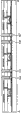
下面将对一种根据本发明的IC片材结构(也称作IC薄膜、片状元件以及膜状元件)进行描述。根据本发明的IC片材是指从两个表面附着在大量薄膜集成电路13中每一个上的第二基底18和第三基底19,它们被卷绕成辊状(参见图13中的IC片材横剖视图)。大量薄膜集成电路13中的每一个均具有大量的元件和一个用作天线的导电层。各个薄膜集成电路13均规则排列。
如前所述,包括大量利用一对密封用基底密封起来的薄膜集成电路13的薄片状IC片材,易于运输。尤其是,在运输大批量的薄膜集成电路13时更为有益。还有,当相互被切开时,大量的薄膜集成电路13将难以搬运;但是由本发明形成的IC片材呈薄片形状,从而使得易于搬运,并且可以防止薄膜集成电路13遭受破坏和损伤。
实施方式3
下面将对一种根据本发明的卷材结构(也称作卷绕元件、卷体或者类似名称)进行描述。根据本发明的卷材由基底卷绕而成,更具体地说,由密封大量薄膜集成电路13中每一个的第二基底18和第三基底19卷绕成卷状(参见图12A中所示卷材的横剖视图和图12B中所示卷材的透视图)。大量薄膜集成电路13中的每一个均具有大量的元件和一个用作天线的导电薄膜。这些薄膜集成电路13均规则排列。
如前所述,由大量利用一对基底密封起来的薄膜集成电路13卷绕而成的卷材,可以轻易运输。尤其是,在运输大批量的薄膜集成电 路13时更为有益。还有,当相互被切开时,大量的薄膜集成电路13将难以搬运;但是由本发明提供的卷材被卷绕起来,从而使得易于搬运,并且可以防止薄膜集成电路13遭受破坏和损伤。
实施方式4
下面将参照附图对一种根据本发明用于制造IC芯片的方法进行描述。
首先,在具有绝缘表面的第一基底100上形成释放层101至103(图5A)。具有绝缘表面的第一基底100对应于剥离基底、石英基底、塑料基底、由诸如丙烯酸树脂这样的柔性合成材料制成的树脂基底、金属基底或者硅基底。需要注意的是,在使用硅基底的情况下,无需设置释放层。
释放层101至103是含硅层,它们利用溅射、等离子体CVD或者类似技术形成。含硅层对应于非晶形半导体层、其中混杂有非晶状态和结晶状态的半非晶形半导体层或者结晶半导体层。
释放层101至103均由一个选自于下述元素的元素层制成:钨(W)、钼(Mo)、钛(Ti)、钽(Ta)、铌(Nb)、镍(Ni)、钴(Co)、锆(Zr)、锌(Zn)、钌(Ru)、铑(Rh)、钯(Pd)、锇(Os)、铱(Ir)、硅(Si)、合金材料或者含有元素作为主要成分的合成材料,它们利用已知方法(比如溅射或者等离子体CVD技术)制成。所述释放层均可以具有单层结构或者多层结构。
释放层101至103被选择性地形成于第一基底100上。其俯视图在图8中示出。图5A和5B均示出了沿着图8中的线A-B的横剖视图。这种选择性形成依次实施,以防止在将释放层101至103去除之后大量设置于释放层101至103上的薄膜集成电路112、118和119发生弥散。
接下来,在释放层101至103上形成一个绝缘底膜104。接下来,在绝缘层104上形成一个元件组105。元件组105包括一个薄膜晶体 管、一个电容、一个电阻、一个二极管或者大量的对应元件。接下来,形成一个绝缘膜108来覆盖住元件组105,并且在绝缘膜108上形成一个绝缘膜109。在绝缘膜109上形成一个用作天线的导电层110。还有,在导电层110上形成一个用作防护膜的绝缘膜111。通过前述步骤,包括元件组105和导电层110的薄膜集成电路112、118和119得以制造完毕。
绝缘膜108、109和111均由一种有机材料或者无机材料制成。聚酰亚胺、丙烯酸树脂、聚酰胺、硅氧烷、环氧树脂或者类似材料可以被用作有机材料。包括由硅(Si)-氧(O)键形成的骨架的硅氧烷和包含氢的有机基团(例如烷基团或者芳香烃)、含氟基团或者含有氢和氟基团的有机基团用作替代物。氧化硅、氮化硅、氧氮化硅、氮氧化硅(silicon nitride oxide)或者类似材料被用作无机材料。
取代选择性地形成释放层101至103,绝缘膜111可以具有较大的厚度,用于防止薄膜集成电路112、118和119发生分散。当绝缘膜111的厚度超过正常值时,由于绝缘膜111的重量,可以防止薄膜集成电路112、118和119发生分散。
接下来,分别在薄膜集成电路112、118和119之间形成开口114至117,以便显露出释放层101至103(图5B)。开口114至117通过利用掩模进行蚀刻、切割成片等等工艺形成。
接着,将一种用于去除释放层101至103的蚀刻剂导入开口114至117内,来使得它们逐步缩减,由此将释放层101至103去除(图6A)。一种含有卤素氟化物的气体或者液体被用作蚀刻剂。例如,三氟化氯(ClF3)被用作一种卤素氟化物。
替代性地,三氟化氮(NF3)、三氟化溴(BrF3)或者氟化氢(HF)可以被用作一种卤素氟化物。需要注意的是,在形成一个含硅层作为释放层的情况下使用氟化氢。
还有,如前所述,由于释放层101至103在这里选择地形成;因此,在将释放层101至103去除之后,绝缘膜104的一部分与第一基 底100接触。因此,可以防止薄膜集成电路112、118和119发生分散。
接下来,将薄膜集成电路112、118和119中每一个的第一表面附着在一个第二基底121。相应地,薄膜集成电路112、118和119与第一基底100分离开。
在前述步骤中,一部分绝缘膜104残留在第一基底100上;但是,本发明并不局限于此。在第一基底100与绝缘膜104之间粘结力较低的情况下,绝缘膜104将通过实施前述步骤完全与第一基底100分离开。
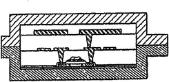
接下来,薄膜集成电路112、118和119的第二表面被附着在一个第三基底122上,并且薄膜集成电路112、118和119被密封在第二基底121与第三基底122之间(图6B)。由此,利用第二基底121和第三基底122将薄膜集成电路112、118和119密封起来。
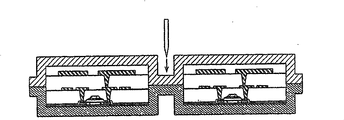
在相应薄膜集成电路112、118和119之间,利用切割成片、划线或者激光切割工艺对第二基底121和第三基底122中每一个的一部分进行切割。由此,一种密封起来的IC芯片得以制造完毕(图7A和7B)。
通过前述步骤密封起来的IC芯片的尺寸为5毫米×5毫米(25mm2)或者更小,优选的是0.3毫米×0.3毫米(0.09mm2)至4毫米×4毫米(16mm2)。
由于根据本发明在无需使用硅基底的条件下将形成于绝缘基底上的薄膜集成电路用于IC芯片,因此与由圆形硅晶片制取的芯片相比,这种IC芯片对母基底形状的限制较少。这样就提高了IC芯片的生产率,并且能够大批量生产这种IC芯片。因此,可以降低IC芯片的成本。还有,根据本发明,厚度为0.2微米或者更薄的半导体膜被用于IC芯片,一般为40纳米至170纳米,优选的是50纳米至150纳米,因此与由硅基底制取的芯片相比,这种IC芯片非常薄。由此,即使当施用在物品上时,也难以注意到薄膜集成电路的存在,这样能 够防止伪造。还有,与由硅基底制取的IC芯片相比,根据本发明的IC芯片可以在没有电磁波吸收的条件下以较高敏感度接收信号。在不使用硅基底的情况下,薄膜集成电路可以具有透光性能。因此,根据本发明的IC芯片可以施用在各种物品上,例如可以在不损坏图案的条件下安置于印刷表面上。本实施方式可以自由地与任一前述实施方式自由组合。
实施例1
利用根据本发明的层压系统制成的IC芯片包括大量的元件,和一个用作天线的导电层。所述大量元件例如对应于薄膜晶体管、电容、电阻和二极管。
IC芯片210具有一种在不发生接触的条件下传送数据的功能,并且构成了各种电路。例如,设置有电源电路211、时钟脉冲发生电路212、数据解调/调制电路213、控制电路214(例如对应于CPU或者MPU)、接口电路215、存储器216、数据总线217、天线(也被称作天线线圈)218以及类似电路(图9)。
电源电路211是一个基于从天线218输入的AC信号产生出即将供给前述相应电路的各种能源的电路。时钟脉冲发生电路212是一个用来基于从天线218输入的AC信号产生出各种即将供给前述相应电路的时钟脉冲的电路。解调/调制电路213具有一种对数据进行解调/调制来与读取器/记录器219交互数据的功能。控制电路214例如对应于中央处理器(CPU)、微处理器(MPU)或者类似器件,并且具有一种对其它电路进行控制的功能。天线218具有一种发射和接收电磁波的功能。读取器/记录器219对处理过程进行控制,这些处理涉及与薄膜集成电路进行通讯、对薄膜集成电路进行控制以及薄膜集成电路中的数据。
由薄膜集成电路构成的电路的结构并不局限于前述结构。例如,可以使用一种带有其它组成部件的结构,比如用于源电压的限幅电路 或者专用于进行加密处理的硬件。
实施例2
利用根据本发明的层压系统制得的IC芯片得以广泛使用。例如,IC芯片210可以被应用在纸币、硬币、有价证券、不记名债券、证书(比如驾驶员执照、居民身份证(图10A)、外包装(比如包裹材料或者瓶子(图10B))、存储介质(比如DVD、录像带(图10C))、车辆(比如自行车(图10D))、财物(比如包、眼镜(图10E))、食品、衣物、商品、以及电子产品。电子产品包括液晶显示设备、EL显示设备、电视设备(也称作电视机(TV)或者电视接收机)、以及蜂窝电话。
IC芯片通过将其附着在物品的表面上、包埋在物品中或者类似处理而固定在物品上。例如,IC芯片可以被包埋在书本的纸张中,或者包埋在由有机树脂制成的包装件的有机树脂中。纸币、硬币、有价证券、不记名债券、证书或者类似物品可以带有一个IC芯片,从而防止伪造。还有,外包装、存储介质、财物、食品、商品以及电子设备可以带有IC芯片,从而可以提高检查系统、用于出租商店的系统以及类似系统的效率。车辆可以带有IC芯片,从而可以防止伪造或者盗抢。
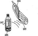
还有,IC芯片可以被应用于商品管理和商品销售系统,从而可以改善系统的功能性。例如,包括显示区域294的便携式终端的侧表面带有一个读取器/记录器295,并且物品297的侧表面带有一个IC芯片296(图11A)。在这种情况下,当IC芯片296被读取器/记录器295感知到时,物品297的信息,比如原材料、原产地、销售历史或者类似信息,会显示在显示区域294上。替代性地,可以在传送带的侧面上设置一个读取器/记录器305(图11B)。在这种情况下,可以利用设置在物品297侧表面上的IC芯片306轻易地对物品397进行检查。
Claims (11)
1.一种用于制造半导体器件的方法,包括下述步骤:
在第一基底之上形成薄膜集成电路,每个所述薄膜集成电路包含薄膜晶体管;
将所述第一基底附着在第二基底上,并将所述薄膜集成电路置于所述第一基底和所述第二基底之间;
将所述薄膜集成电路从所述第一基底分离;
将所述第二基底附着在第三基底上,使得所述薄膜集成电路被密封在所述第二基底和所述第三基底之间;和
利用激光将所述第二基底和所述第三基底切割成多个芯片,每个芯片包含至少一个所述薄膜集成电路。
2.一种用于制造半导体器件的方法,包括下述步骤:
在第一基底之上形成薄膜集成电路,每个所述薄膜集成电路包含薄膜晶体管和天线;
将所述第一基底附着在第二基底上,并将所述薄膜集成电路置于所述两基底之间;
将所述薄膜集成电路从所述第一基底分离;
将所述第二基底附着在第三基底上,使得所述薄膜集成电路被密封在所述第二基底和所述第三基底之间;和
利用激光将所述第二基底和所述第三基底切割成多个芯片,每个芯片包含至少一个所述薄膜集成电路。
3.一种用于制造半导体器件的方法,包括下述步骤:
在第一基底之上形成薄膜集成电路,每个所述薄膜集成电路包含薄膜晶体管;
将所述第一基底附着在第二基底上,并将所述薄膜集成电路置于所述第一基底和所述第二基底之间;
将所述薄膜集成电路从所述第一基底分离;
将所述第二基底附着在第三基底上,使得所述薄膜集成电路被密封在所述第二基底和所述第三基底之间;和
利用激光将所述第二基底和所述第三基底切割成多个芯片,每个芯片包含至少一个所述薄膜集成电路,
其中,所述第二基底和所述第三基底中的至少一个基底涂有导电材料。
4.一种用于制造半导体器件的方法,包括下述步骤:
在第一基底之上形成薄膜集成电路,每个所述薄膜集成电路包含薄膜晶体管和天线;
将所述第一基底附着在第二基底上,并将所述薄膜集成电路置于所述两基底之间;
将所述薄膜集成电路从所述第一基底分离;
将所述第二基底附着在第三基底上,使得所述薄膜集成电路被密封在所述第二基底和所述第三基底之间;和
利用激光将所述第二基底和所述第三基底切割成多个芯片,每个芯片包含至少一个所述薄膜集成电路,
其中,所述第二基底和所述第三基底中的至少一个基底涂有导电材料。
5.根据权利要求1、2、3、4中的任意一项所述的用于制造半导体器件的方法,其特征在于,所述第二基底和所述第三基底包含层压膜或者由纤维材料制成的纸张。
6.根据权利要求1、2、3、4中的任意一项所述的用于制造半导体器件的方法,其特征在于,所述第二基底和所述第三基底包含由聚丙烯、聚酯、聚氟乙烯、聚氯乙烯、聚乙烯和乙烯-醋酸乙烯酯所组成的组中选择的至少一种物质。
7.根据权利要求1、2、3、4中的任意一项所述的用于制造半导体器件的方法,其特征在于,所述第二基底和所述第三基底的至少一个表面涂有粘合剂。
8.根据权利要求3或4所述的用于制造半导体器件的方法,其特征在于,所述导电材料包含碳或氧化铟锡。
9.根据权利要求1、2、3、4中的任意一项所述的用于制造半导体器件的方法,其特征在于,通过执行压力处理和加热处理中的一种处理,将所述薄膜集成电路密封于所述第二基底和所述第三基底之间。
10.根据权利要求1、2、3、4中的任意一项所述的用于制造半导体器件的方法,其特征在于,所述多个芯片中的每个芯片都能够传送数据而不发生接触。
11.根据权利要求1、2、3、4中的任意一项所述的用于制造半导体器件的方法,其特征在于,通过将所述第二基底附着在所述第三基底上的步骤,所述第二基底和所述第三基底在位于所述薄膜集成电路外侧的区域彼此接触。
Applications Claiming Priority (2)
| Application Number | Priority Date | Filing Date | Title |
|---|---|---|---|
| JP2004165104 | 2004-06-02 | ||
| JP2004-165104 | 2004-06-02 |
Related Parent Applications (1)
| Application Number | Title | Priority Date | Filing Date |
|---|---|---|---|
| CN2005800262291A Division CN1993829B (zh) | 2004-06-02 | 2005-05-31 | 层压系统 |
Publications (2)
| Publication Number | Publication Date |
|---|---|
| CN101789378A CN101789378A (zh) | 2010-07-28 |
| CN101789378B true CN101789378B (zh) | 2012-07-04 |
Family
ID=35463135
Family Applications (3)
| Application Number | Title | Priority Date | Filing Date |
|---|---|---|---|
| CN2005800262291A Expired - Fee Related CN1993829B (zh) | 2004-06-02 | 2005-05-31 | 层压系统 |
| CN2009101180509A Expired - Fee Related CN101527270B (zh) | 2004-06-02 | 2005-05-31 | 一种半导体设备 |
| CN2009100028576A Expired - Fee Related CN101789378B (zh) | 2004-06-02 | 2005-05-31 | 用于制造半导体器件的方法 |
Family Applications Before (2)
| Application Number | Title | Priority Date | Filing Date |
|---|---|---|---|
| CN2005800262291A Expired - Fee Related CN1993829B (zh) | 2004-06-02 | 2005-05-31 | 层压系统 |
| CN2009101180509A Expired - Fee Related CN101527270B (zh) | 2004-06-02 | 2005-05-31 | 一种半导体设备 |
Country Status (6)
| Country | Link |
|---|---|
| US (3) | US8123896B2 (zh) |
| EP (1) | EP1774595A4 (zh) |
| JP (1) | JP4579057B2 (zh) |
| KR (5) | KR101226260B1 (zh) |
| CN (3) | CN1993829B (zh) |
| WO (1) | WO2005119781A1 (zh) |
Families Citing this family (85)
| Publication number | Priority date | Publication date | Assignee | Title |
|---|---|---|---|---|
| US7487373B2 (en) | 2004-01-30 | 2009-02-03 | Semiconductor Energy Laboratory Co., Ltd. | Wireless semiconductor device having low power consumption |
| US7820529B2 (en) * | 2004-03-22 | 2010-10-26 | Semiconductor Energy Laboratory Co., Ltd. | Method for manufacturing integrated circuit |
| KR101226260B1 (ko) * | 2004-06-02 | 2013-01-28 | 가부시키가이샤 한도오따이 에네루기 켄큐쇼 | 반도체장치 제조방법 |
| US7591863B2 (en) * | 2004-07-16 | 2009-09-22 | Semiconductor Energy Laboratory Co., Ltd. | Laminating system, IC sheet, roll of IC sheet, and method for manufacturing IC chip |
| KR101254277B1 (ko) | 2004-07-30 | 2013-04-15 | 가부시키가이샤 한도오따이 에네루기 켄큐쇼 | 라미네이팅 시스템, ic 시트, ic 시트 두루마리, 및ic 칩의 제조방법 |
| US20150287660A1 (en) | 2007-01-05 | 2015-10-08 | Semiconductor Energy Laboratory Co., Ltd. | Laminating system, ic sheet, scroll of ic sheet, and method for manufacturing ic chip |
| CN100474629C (zh) | 2004-08-23 | 2009-04-01 | 株式会社半导体能源研究所 | 无线芯片及其制造方法 |
| US8153511B2 (en) * | 2005-05-30 | 2012-04-10 | Semiconductor Energy Laboratory Co., Ltd. | Method for manufacturing semiconductor device |
| US7605056B2 (en) | 2005-05-31 | 2009-10-20 | Semiconductor Energy Laboratory Co., Ltd. | Method of manufacturing a semiconductor device including separation by physical force |
| US7776656B2 (en) | 2005-07-29 | 2010-08-17 | Semiconductor Energy Laboratory Co., Ltd. | Method for manufacturing semiconductor device |
| EP1920459A4 (en) | 2005-08-12 | 2012-07-25 | Semiconductor Energy Lab | PROCESS FOR PRODUCING A SEMICONDUCTOR COMPONENT |
| WO2007063786A1 (en) | 2005-11-29 | 2007-06-07 | Semiconductor Energy Laboratory Co., Ltd. | Antenna and manufacturing method thereof, semiconductor device including antenna and manufacturing method thereof, and radio communication system |
| US7504317B2 (en) | 2005-12-02 | 2009-03-17 | Semiconductor Energy Laboratory Co., Ltd. | Manufacturing method of semiconductor device |
| US20070183184A1 (en) | 2006-02-03 | 2007-08-09 | Semiconductor Energy Laboratory Ltd. | Apparatus and method for manufacturing semiconductor device |
| JP4799204B2 (ja) * | 2006-02-09 | 2011-10-26 | 株式会社半導体エネルギー研究所 | 温度センサ素子、表示装置および半導体装置 |
| CN101385039B (zh) * | 2006-03-15 | 2012-03-21 | 株式会社半导体能源研究所 | 半导体器件 |
| JP4910689B2 (ja) * | 2006-06-12 | 2012-04-04 | ブラザー工業株式会社 | タグテープロール製造装置 |
| JP5204959B2 (ja) * | 2006-06-26 | 2013-06-05 | 株式会社半導体エネルギー研究所 | 半導体装置の作製方法 |
| CN101479747B (zh) | 2006-06-26 | 2011-05-18 | 株式会社半导体能源研究所 | 包括半导体器件的纸及其制造方法 |
| TWI424499B (zh) * | 2006-06-30 | 2014-01-21 | Semiconductor Energy Lab | 製造半導體裝置的方法 |
| FR2906078B1 (fr) * | 2006-09-19 | 2009-02-13 | Commissariat Energie Atomique | Procede de fabrication d'une structure micro-technologique mixte et une structure ainsi obtenue |
| TWI430435B (zh) * | 2006-09-29 | 2014-03-11 | Semiconductor Energy Lab | 半導體裝置的製造方法 |
| US8137417B2 (en) | 2006-09-29 | 2012-03-20 | Semiconductor Energy Laboratory Co., Ltd. | Peeling apparatus and manufacturing apparatus of semiconductor device |
| EP1976001A3 (en) * | 2007-03-26 | 2012-08-22 | Semiconductor Energy Laboratory Co., Ltd. | Method for manufacturing semiconductor device |
| EP1976000A3 (en) * | 2007-03-26 | 2009-05-13 | Semiconductor Energy Laboratory Co., Ltd. | Method for manufacturing semiconductor device |
| US7851334B2 (en) * | 2007-07-20 | 2010-12-14 | Infineon Technologies Ag | Apparatus and method for producing semiconductor modules |
| JP5460108B2 (ja) | 2008-04-18 | 2014-04-02 | 株式会社半導体エネルギー研究所 | 半導体装置及び半導体装置の作製方法 |
| KR101596698B1 (ko) | 2008-04-25 | 2016-02-24 | 가부시키가이샤 한도오따이 에네루기 켄큐쇼 | 반도체 장치 및 반도체 장치 제조 방법 |
| KR101582503B1 (ko) | 2008-05-12 | 2016-01-05 | 가부시키가이샤 한도오따이 에네루기 켄큐쇼 | 반도체 장치 및 반도체 장치의 제작 방법 |
| WO2009142310A1 (en) * | 2008-05-23 | 2009-11-26 | Semiconductor Energy Laboratory Co., Ltd. | Semiconductor device and method for manufacturing the same |
| WO2009142309A1 (en) * | 2008-05-23 | 2009-11-26 | Semiconductor Energy Laboratory Co., Ltd. | Semiconductor device |
| JP5248412B2 (ja) * | 2008-06-06 | 2013-07-31 | 株式会社半導体エネルギー研究所 | 半導体装置の作製方法 |
| US8053253B2 (en) | 2008-06-06 | 2011-11-08 | Semiconductor Energy Laboratory Co., Ltd. | Method for manufacturing semiconductor device |
| CN103500700B (zh) * | 2008-06-06 | 2016-06-08 | 株式会社半导体能源研究所 | 半导体装置的制造方法 |
| US8044499B2 (en) * | 2008-06-10 | 2011-10-25 | Semiconductor Energy Laboratory Co., Ltd. | Wiring substrate, manufacturing method thereof, semiconductor device, and manufacturing method thereof |
| JP2010041045A (ja) * | 2008-07-09 | 2010-02-18 | Semiconductor Energy Lab Co Ltd | 半導体装置及びその作製方法 |
| TWI475282B (zh) * | 2008-07-10 | 2015-03-01 | Semiconductor Energy Lab | 液晶顯示裝置和其製造方法 |
| KR101925772B1 (ko) | 2008-07-10 | 2018-12-06 | 가부시키가이샤 한도오따이 에네루기 켄큐쇼 | 발광 장치 및 전자 기기 |
| JP5216716B2 (ja) | 2008-08-20 | 2013-06-19 | 株式会社半導体エネルギー研究所 | 発光装置及びその作製方法 |
| KR100947350B1 (ko) * | 2008-08-26 | 2010-03-15 | (주)상아프론테크 | 엘씨디 기판 적재 카세트용 바아 |
| WO2010032602A1 (en) | 2008-09-18 | 2010-03-25 | Semiconductor Energy Laboratory Co., Ltd. | Semiconductor device |
| WO2010032611A1 (en) * | 2008-09-19 | 2010-03-25 | Semiconductor Energy Laboratory Co., Ltd. | Semiconductor device and method for manufacturing the same |
| US8361840B2 (en) * | 2008-09-24 | 2013-01-29 | Eastman Kodak Company | Thermal barrier layer for integrated circuit manufacture |
| WO2010035625A1 (en) * | 2008-09-25 | 2010-04-01 | Semiconductor Energy Laboratory Co., Ltd. | Semi conductor device |
| WO2010035627A1 (en) * | 2008-09-25 | 2010-04-01 | Semiconductor Energy Laboratory Co., Ltd. | Semiconductor device |
| KR101611643B1 (ko) * | 2008-10-01 | 2016-04-11 | 가부시키가이샤 한도오따이 에네루기 켄큐쇼 | 반도체 장치 |
| JP5586920B2 (ja) * | 2008-11-20 | 2014-09-10 | 株式会社半導体エネルギー研究所 | フレキシブル半導体装置の作製方法 |
| TWI517268B (zh) * | 2009-08-07 | 2016-01-11 | 半導體能源研究所股份有限公司 | 端子構造的製造方法和電子裝置的製造方法 |
| KR101020087B1 (ko) * | 2009-09-23 | 2011-03-09 | 한국철강 주식회사 | 광기전력 장치의 제조 방법 |
| JP5719560B2 (ja) * | 2009-10-21 | 2015-05-20 | 株式会社半導体エネルギー研究所 | 端子構造の作製方法 |
| US10541160B2 (en) | 2009-12-29 | 2020-01-21 | Nikon Corporation | Substrate case and substrate accommodation apparatus |
| JP2011186590A (ja) * | 2010-03-05 | 2011-09-22 | Dainippon Printing Co Ltd | 非接触icカード、非接触icカードの製造方法 |
| JP5616119B2 (ja) * | 2010-05-10 | 2014-10-29 | 株式会社アドバンテスト | 試験用キャリア |
| DE102011112964A1 (de) * | 2011-09-15 | 2013-03-21 | Evonik Industries Ag | PV-PSA-Laminat durch PSA-Lamination auf einen Release-Film |
| KR101284666B1 (ko) * | 2011-11-01 | 2013-07-10 | 현대다이모스(주) | 연질 슬라브재와 피복의 부착장치 및 피복 지그 |
| JPWO2013191026A1 (ja) * | 2012-06-22 | 2016-05-26 | 株式会社シンク・ラボラトリー | プリント回路基板の製造装置並びに製造方法 |
| US20140087198A1 (en) * | 2012-09-26 | 2014-03-27 | Web Industries, Inc. | Prepreg tape slitting method and apparatus |
| KR102224416B1 (ko) | 2013-08-06 | 2021-03-05 | 가부시키가이샤 한도오따이 에네루기 켄큐쇼 | 박리 방법 |
| TW201943069A (zh) | 2013-09-06 | 2019-11-01 | 日商半導體能源研究所股份有限公司 | 發光裝置以及發光裝置的製造方法 |
| US9981457B2 (en) | 2013-09-18 | 2018-05-29 | Semiconductor Emergy Laboratory Co., Ltd. | Manufacturing apparatus of stack |
| JP6513929B2 (ja) | 2013-11-06 | 2019-05-15 | 株式会社半導体エネルギー研究所 | 剥離方法 |
| CN110010625A (zh) | 2013-12-02 | 2019-07-12 | 株式会社半导体能源研究所 | 显示装置及其制造方法 |
| US9427949B2 (en) | 2013-12-03 | 2016-08-30 | Semiconductor Energy Laboratory Co., Ltd. | Peeling apparatus and stack manufacturing apparatus |
| US10315399B2 (en) * | 2013-12-31 | 2019-06-11 | Entrotech, Inc. | Methods for application of polymeric film and related assemblies |
| US9676175B2 (en) | 2014-06-20 | 2017-06-13 | Semiconductor Energy Laboratory Co., Ltd. | Peeling apparatus |
| TWI695525B (zh) | 2014-07-25 | 2020-06-01 | 日商半導體能源研究所股份有限公司 | 剝離方法、發光裝置、模組以及電子裝置 |
| JP6815096B2 (ja) | 2015-05-27 | 2021-01-20 | 株式会社半導体エネルギー研究所 | 剥離装置 |
| KR102632066B1 (ko) * | 2015-07-30 | 2024-02-02 | 가부시키가이샤 한도오따이 에네루기 켄큐쇼 | 발광 장치의 제작 방법, 발광 장치, 모듈, 및 전자 기기 |
| CN106469772B (zh) * | 2015-08-18 | 2018-01-05 | 江苏诚睿达光电有限公司 | 一种基于滚压式的热塑性树脂光转换体贴合封装led的工艺方法 |
| CN106469768B (zh) * | 2015-08-18 | 2018-02-02 | 江苏诚睿达光电有限公司 | 一种异形有机硅树脂光转换体贴合封装led的装备系统 |
| US10259207B2 (en) | 2016-01-26 | 2019-04-16 | Semiconductor Energy Laboratory Co., Ltd. | Method for forming separation starting point and separation method |
| US10586817B2 (en) | 2016-03-24 | 2020-03-10 | Semiconductor Energy Laboratory Co., Ltd. | Semiconductor device, manufacturing method thereof, and separation apparatus |
| JP6312270B2 (ja) * | 2016-03-25 | 2018-04-18 | 株式会社写真化学 | デバイスチップを用いた電子デバイスの製造方法およびその製造装置 |
| KR102340066B1 (ko) | 2016-04-07 | 2021-12-15 | 가부시키가이샤 한도오따이 에네루기 켄큐쇼 | 박리 방법 및 플렉시블 디바이스의 제작 방법 |
| US10003023B2 (en) | 2016-04-15 | 2018-06-19 | Semiconductor Energy Laboratory Co., Ltd. | Display device and electronic device |
| JP2017207744A (ja) | 2016-05-11 | 2017-11-24 | 株式会社半導体エネルギー研究所 | 表示装置、モジュール、及び電子機器 |
| EP3479401A4 (en) | 2016-07-01 | 2020-03-04 | INTEL Corporation | SEMICONDUCTOR HOUSING WITH ANTENNAS |
| KR102554183B1 (ko) | 2016-07-29 | 2023-07-10 | 가부시키가이샤 한도오따이 에네루기 켄큐쇼 | 박리 방법, 표시 장치, 표시 모듈, 및 전자 기기 |
| TW201808628A (zh) | 2016-08-09 | 2018-03-16 | Semiconductor Energy Lab | 半導體裝置的製造方法 |
| TWI730017B (zh) | 2016-08-09 | 2021-06-11 | 日商半導體能源研究所股份有限公司 | 顯示裝置的製造方法、顯示裝置、顯示模組及電子裝置 |
| KR102028027B1 (ko) * | 2017-03-14 | 2019-10-04 | (주)잉크테크 | 반도체 칩의 전자파 차폐막 형성 장치 및 방법 |
| CN109748090A (zh) * | 2017-11-02 | 2019-05-14 | 何崇文 | 贴拆板机台及其加工方法 |
| KR102154811B1 (ko) * | 2018-10-29 | 2020-09-11 | 한국기계연구원 | 필름 전사 방법 |
| AR118939A1 (es) * | 2020-05-15 | 2021-11-10 | Marisa Rosana Lattanzi | Máquina combinada para elaborar separadores laminares de productos que se contienen en cajas y cajones |
| KR102288594B1 (ko) * | 2021-02-26 | 2021-08-11 | 주식회사 이송이엠씨 | 박막 fmcl 제조 장치 및 박막 fmcl 제조 방법 |
Family Cites Families (108)
| Publication number | Priority date | Publication date | Assignee | Title |
|---|---|---|---|---|
| FR2524679B1 (fr) | 1982-04-01 | 1990-07-06 | Suwa Seikosha Kk | Procede d'attaque d'un panneau d'affichage a cristaux liquides a matrice active |
| DE3325578C2 (de) * | 1983-07-15 | 1985-11-14 | Held, Kurt, 7218 Trossingen | Doppelbandpresse zur kontinuierlichen Herstellung von Laminaten |
| US4743334A (en) | 1986-02-19 | 1988-05-10 | D&K Custom Machine Design, Inc. | Double sided laminating machine |
| JPH0219271A (ja) * | 1988-07-06 | 1990-01-23 | Toshiba Corp | 半導体装置用テーピング部品 |
| US4897662A (en) | 1988-12-09 | 1990-01-30 | Dallas Semiconductor Corporation | Integrated circuit with wireless freshness seal |
| US5203941A (en) | 1989-10-19 | 1993-04-20 | Avery Dennison Corporation | Process for manufacturing plastic siding panels with outdoor weatherable embossed surfaces |
| EP0438138B1 (en) | 1990-01-17 | 1995-03-15 | Kabushiki Kaisha Toshiba | Liquid-crystal display device of active matrix type |
| US5258320A (en) * | 1990-12-31 | 1993-11-02 | Kopin Corporation | Single crystal silicon arrayed devices for display panels |
| US5274602A (en) * | 1991-10-22 | 1993-12-28 | Florida Atlantic University | Large capacity solid-state memory |
| JPH0621443Y2 (ja) | 1991-11-21 | 1994-06-08 | 株式会社ニッショー | 減圧採血管 |
| JPH0774282B2 (ja) | 1992-01-29 | 1995-08-09 | ゼネラル・エレクトリック・カンパニイ | アクリルコ―トしたポリカ―ボネ―ト物品の製造方法 |
| US5461338A (en) | 1992-04-17 | 1995-10-24 | Nec Corporation | Semiconductor integrated circuit incorporated with substrate bias control circuit |
| JP3254007B2 (ja) | 1992-06-09 | 2002-02-04 | 株式会社半導体エネルギー研究所 | 薄膜状半導体装置およびその作製方法 |
| US5807772A (en) | 1992-06-09 | 1998-09-15 | Semiconductor Energy Laboratory Co., Ltd. | Method for forming semiconductor device with bottom gate connected to source or drain |
| JP2974552B2 (ja) | 1993-06-14 | 1999-11-10 | 株式会社東芝 | 半導体装置 |
| US5477073A (en) | 1993-08-20 | 1995-12-19 | Casio Computer Co., Ltd. | Thin film semiconductor device including a driver and a matrix circuit |
| JPH07131030A (ja) | 1993-11-05 | 1995-05-19 | Sony Corp | 表示用薄膜半導体装置及びその製造方法 |
| JPH07134572A (ja) | 1993-11-11 | 1995-05-23 | Nec Corp | アクティブマトリクス型液晶表示装置の駆動回路 |
| US7081938B1 (en) | 1993-12-03 | 2006-07-25 | Semiconductor Energy Laboratory Co., Ltd. | Electro-optical device and method for manufacturing the same |
| JP3175894B2 (ja) | 1994-03-25 | 2001-06-11 | 株式会社半導体エネルギー研究所 | プラズマ処理装置及びプラズマ処理方法 |
| JP3253808B2 (ja) | 1994-07-07 | 2002-02-04 | 株式会社半導体エネルギー研究所 | 半導体装置およびその作製方法 |
| JP3698749B2 (ja) | 1995-01-11 | 2005-09-21 | 株式会社半導体エネルギー研究所 | 液晶セルの作製方法およびその作製装置、液晶セルの生産システム |
| US5757456A (en) | 1995-03-10 | 1998-05-26 | Semiconductor Energy Laboratory Co., Ltd. | Display device and method of fabricating involving peeling circuits from one substrate and mounting on other |
| JP3579492B2 (ja) | 1995-03-16 | 2004-10-20 | 株式会社半導体エネルギー研究所 | 表示装置の作製方法 |
| US5705022A (en) * | 1995-06-08 | 1998-01-06 | International Business Machines Corporation | Continuous lamination of electronic structures |
| JP3708554B2 (ja) | 1995-08-04 | 2005-10-19 | セイコーエプソン株式会社 | 薄膜トランジスタの製造方法 |
| JP3647523B2 (ja) | 1995-10-14 | 2005-05-11 | 株式会社半導体エネルギー研究所 | マトリクス型液晶表示装置 |
| JP3409542B2 (ja) | 1995-11-21 | 2003-05-26 | ソニー株式会社 | 半導体装置の製造方法 |
| US5814834A (en) | 1995-12-04 | 1998-09-29 | Semiconductor Energy Laboratory Co. | Thin film semiconductor device |
| US6342434B1 (en) * | 1995-12-04 | 2002-01-29 | Hitachi, Ltd. | Methods of processing semiconductor wafer, and producing IC card, and carrier |
| JP3516424B2 (ja) | 1996-03-10 | 2004-04-05 | 株式会社半導体エネルギー研究所 | 薄膜半導体装置 |
| JPH1092980A (ja) | 1996-09-13 | 1998-04-10 | Toshiba Corp | 無線カードおよびその製造方法 |
| JP3424891B2 (ja) | 1996-12-27 | 2003-07-07 | 三洋電機株式会社 | 薄膜トランジスタの製造方法および表示装置 |
| KR100506099B1 (ko) | 1997-02-24 | 2005-09-26 | 산요덴키가부시키가이샤 | 다결정실리콘막제조방법,박막트랜지스터제조방법,및어닐링장치 |
| US6010923A (en) | 1997-03-31 | 2000-01-04 | Sanyo Electric Co., Ltd. | Manufacturing method of semiconductor device utilizing annealed semiconductor layer as channel region |
| JP3376247B2 (ja) | 1997-05-30 | 2003-02-10 | 株式会社半導体エネルギー研究所 | 薄膜トランジスタ及び薄膜トランジスタを用いた半導体装置 |
| US6197624B1 (en) | 1997-08-29 | 2001-03-06 | Semiconductor Energy Laboratory Co., Ltd. | Method of adjusting the threshold voltage in an SOI CMOS |
| JP3552500B2 (ja) | 1997-11-12 | 2004-08-11 | セイコーエプソン株式会社 | 論理振幅レベル変換回路,液晶装置及び電子機器 |
| US6285248B1 (en) | 1997-11-13 | 2001-09-04 | Seiko Epson Corporation | Semiconductor integrated circuit, operating state detector, and electronic equipment |
| US6922134B1 (en) | 1998-04-14 | 2005-07-26 | The Goodyear Tire Rubber Company | Programmable trimmer for transponder |
| JP2001051292A (ja) | 1998-06-12 | 2001-02-23 | Semiconductor Energy Lab Co Ltd | 半導体装置および半導体表示装置 |
| US6512271B1 (en) | 1998-11-16 | 2003-01-28 | Semiconductor Energy Laboratory Co., Ltd. | Semiconductor device |
| US6447448B1 (en) | 1998-12-31 | 2002-09-10 | Ball Semiconductor, Inc. | Miniature implanted orthopedic sensors |
| EP1020839A3 (en) | 1999-01-08 | 2002-11-27 | Sel Semiconductor Energy Laboratory Co., Ltd. | Semiconductor display device and driving circuit therefor |
| JP4332925B2 (ja) | 1999-02-25 | 2009-09-16 | ソニー株式会社 | 半導体装置およびその製造方法 |
| JP4359357B2 (ja) * | 1999-03-09 | 2009-11-04 | 株式会社瑞光 | ヒートシール装置 |
| US6224965B1 (en) | 1999-06-25 | 2001-05-01 | Honeywell International Inc. | Microfiber dielectrics which facilitate laser via drilling |
| JP4423779B2 (ja) | 1999-10-13 | 2010-03-03 | 味の素株式会社 | エポキシ樹脂組成物並びに該組成物を用いた接着フィルム及びプリプレグ、及びこれらを用いた多層プリント配線板及びその製造法 |
| JP4748859B2 (ja) | 2000-01-17 | 2011-08-17 | 株式会社半導体エネルギー研究所 | 発光装置の作製方法 |
| US7060153B2 (en) * | 2000-01-17 | 2006-06-13 | Semiconductor Energy Laboratory Co., Ltd. | Display device and method of manufacturing the same |
| JP4316767B2 (ja) | 2000-03-22 | 2009-08-19 | 株式会社半導体エネルギー研究所 | 基板処理装置 |
| JP4347496B2 (ja) * | 2000-03-31 | 2009-10-21 | 共同印刷株式会社 | 可逆性感熱記録媒体の製造方法 |
| JP3475237B2 (ja) | 2000-07-24 | 2003-12-08 | 東京大学長 | 電力制御装置及び方法並びに電力制御プログラムを記録した記録媒体 |
| JP3941362B2 (ja) | 2000-09-08 | 2007-07-04 | 日立化成工業株式会社 | 電子タグとそれを用いた電子標識 |
| JP4373595B2 (ja) | 2000-09-25 | 2009-11-25 | 株式会社東芝 | コンピュータシステム |
| US6484780B2 (en) * | 2001-03-21 | 2002-11-26 | Card Technology Corporation | Card laminator and method of card lamination |
| WO2001060112A2 (en) * | 2001-05-23 | 2001-08-16 | Phonak Ag | Method of generating an electrical output signal and acoustical/electrical conversion system |
| JP2003016405A (ja) | 2001-06-28 | 2003-01-17 | Toppan Printing Co Ltd | Icタグ装着方法 |
| JP2003016414A (ja) | 2001-07-05 | 2003-01-17 | Toppan Printing Co Ltd | 非接触方式icチップ付きシート及びその製造方法 |
| JP2003086706A (ja) | 2001-09-13 | 2003-03-20 | Sharp Corp | 半導体装置及びその製造方法、スタティック型ランダムアクセスメモリ装置並びに携帯電子機器 |
| WO2003009385A1 (fr) | 2001-07-19 | 2003-01-30 | Sharp Kabushiki Kaisha | Dispositif a semi-conducteur, dispositif de stockage a semi-conducteur et procedes de production associes |
| US6887650B2 (en) | 2001-07-24 | 2005-05-03 | Seiko Epson Corporation | Transfer method, method of manufacturing thin film devices, method of manufacturing integrated circuits, circuit board and manufacturing method thereof, electro-optical apparatus and manufacturing method thereof, ic card, and electronic appliance |
| JP2003037352A (ja) * | 2001-07-25 | 2003-02-07 | Nitto Denko Corp | 配線回路基板の製造方法 |
| KR100944886B1 (ko) * | 2001-10-30 | 2010-03-03 | 가부시키가이샤 한도오따이 에네루기 켄큐쇼 | 반도체 장치의 제조 방법 |
| US6872658B2 (en) | 2001-11-30 | 2005-03-29 | Semiconductor Energy Laboratory Co., Ltd. | Method of fabricating semiconductor device by exposing resist mask |
| TWI264121B (en) | 2001-11-30 | 2006-10-11 | Semiconductor Energy Lab | A display device, a method of manufacturing a semiconductor device, and a method of manufacturing a display device |
| KR100430001B1 (ko) | 2001-12-18 | 2004-05-03 | 엘지전자 주식회사 | 다층기판의 제조방법, 그 다층기판의 패드 형성방법 및 그다층기판을 이용한 반도체 패키지의 제조방법 |
| FR2833844B1 (fr) * | 2001-12-21 | 2004-11-26 | Airinspace Ltd | Dispositif mobile d'isolement aeraulique contre la contamination aeroportee, a geometrie variable de diffusseur d'air |
| JP3956697B2 (ja) * | 2001-12-28 | 2007-08-08 | セイコーエプソン株式会社 | 半導体集積回路の製造方法 |
| US6883573B2 (en) | 2002-04-04 | 2005-04-26 | Japan Servo Co., Ltd. | Lamination system |
| JP4215998B2 (ja) * | 2002-04-30 | 2009-01-28 | リンテック株式会社 | 半導体ウエハの処理方法およびそのための半導体ウエハの転写装置 |
| US6715524B2 (en) * | 2002-06-07 | 2004-04-06 | Taiwan Semiconductor Manufacturing Co., Ltd. | DFR laminating and film removing system |
| US7485489B2 (en) | 2002-06-19 | 2009-02-03 | Bjoersell Sten | Electronics circuit manufacture |
| AU2003253227A1 (en) | 2002-06-19 | 2004-01-06 | Sten Bjorsell | Electronics circuit manufacture |
| JP2004094492A (ja) | 2002-08-30 | 2004-03-25 | Konica Minolta Holdings Inc | Icカード |
| JP2004110906A (ja) | 2002-09-17 | 2004-04-08 | Renesas Technology Corp | 半導体記憶装置 |
| JP4012025B2 (ja) * | 2002-09-24 | 2007-11-21 | 大日本印刷株式会社 | 微小構造体付きフィルムの製造方法と微小構造体付きフィルム |
| JP4683817B2 (ja) | 2002-09-27 | 2011-05-18 | 株式会社半導体エネルギー研究所 | 半導体装置の作製方法 |
| KR101032337B1 (ko) | 2002-12-13 | 2011-05-09 | 가부시키가이샤 한도오따이 에네루기 켄큐쇼 | 발광장치 및 그의 제조방법 |
| JP4671600B2 (ja) | 2002-12-27 | 2011-04-20 | 株式会社半導体エネルギー研究所 | 半導体装置の作製方法 |
| JP4373085B2 (ja) | 2002-12-27 | 2009-11-25 | 株式会社半導体エネルギー研究所 | 半導体装置の作製方法、剥離方法及び転写方法 |
| EP1434264A3 (en) | 2002-12-27 | 2017-01-18 | Semiconductor Energy Laboratory Co., Ltd. | Semiconductor device and manufacturing method using the transfer technique |
| EP1437683B1 (en) | 2002-12-27 | 2017-03-08 | Semiconductor Energy Laboratory Co., Ltd. | IC card and booking account system using the IC card |
| TWI330269B (en) | 2002-12-27 | 2010-09-11 | Semiconductor Energy Lab | Separating method |
| US7230316B2 (en) | 2002-12-27 | 2007-06-12 | Semiconductor Energy Laboratory Co., Ltd. | Semiconductor device having transferred integrated circuit |
| AU2003289448A1 (en) | 2003-01-08 | 2004-08-23 | Semiconductor Energy Laboratory Co., Ltd. | Semiconductor device and its fabricating method |
| AU2003292609A1 (en) | 2003-01-15 | 2004-08-10 | Semiconductor Energy Laboratory Co., Ltd. | Separating method and method for manufacturing display device using the separating method |
| JP4549866B2 (ja) | 2003-02-05 | 2010-09-22 | 株式会社半導体エネルギー研究所 | 表示装置の製造方法 |
| TWI360702B (en) | 2003-03-07 | 2012-03-21 | Semiconductor Energy Lab | Liquid crystal display device and method for manuf |
| JP4526771B2 (ja) | 2003-03-14 | 2010-08-18 | 株式会社半導体エネルギー研究所 | 半導体装置の作製方法 |
| US7307317B2 (en) | 2003-04-04 | 2007-12-11 | Semiconductor Energy Laboratory Co., Ltd. | Semiconductor device, CPU, image processing circuit and electronic device, and driving method of semiconductor device |
| US7495272B2 (en) | 2003-10-06 | 2009-02-24 | Semiconductor Energy Labortaory Co., Ltd. | Semiconductor device having photo sensor element and amplifier circuit |
| US7011130B2 (en) * | 2003-10-17 | 2006-03-14 | Primera Technology, Inc. | Laminator for applying a protective layer to a disc |
| EP1528594B1 (en) | 2003-10-28 | 2019-05-29 | Semiconductor Energy Laboratory Co., Ltd. | Method for manufacturing semiconductor device |
| US7229900B2 (en) | 2003-10-28 | 2007-06-12 | Semiconductor Energy Laboratory Co., Ltd. | Semiconductor device, method of manufacturing thereof, and method of manufacturing base material |
| US7271076B2 (en) * | 2003-12-19 | 2007-09-18 | Semiconductor Energy Laboratory Co., Ltd. | Manufacturing method of thin film integrated circuit device and manufacturing method of non-contact type thin film integrated circuit device |
| US7554121B2 (en) | 2003-12-26 | 2009-06-30 | Semiconductor Energy Laboratory Co., Ltd. | Organic semiconductor device |
| US7487373B2 (en) | 2004-01-30 | 2009-02-03 | Semiconductor Energy Laboratory Co., Ltd. | Wireless semiconductor device having low power consumption |
| US7820529B2 (en) | 2004-03-22 | 2010-10-26 | Semiconductor Energy Laboratory Co., Ltd. | Method for manufacturing integrated circuit |
| EP1589797A3 (en) | 2004-04-19 | 2008-07-30 | Matsushita Electric Industrial Co., Ltd. | Manufacturing method of laminated substrate, and manufacturing apparatus of semiconductor device for module and laminated substrate for use therein |
| KR101226260B1 (ko) | 2004-06-02 | 2013-01-28 | 가부시키가이샤 한도오따이 에네루기 켄큐쇼 | 반도체장치 제조방법 |
| US7452786B2 (en) | 2004-06-29 | 2008-11-18 | Semiconductor Energy Laboratory Co., Ltd. | Method for manufacturing thin film integrated circuit, and element substrate |
| US7534702B2 (en) | 2004-06-29 | 2009-05-19 | Semiconductor Energy Laboratory Co., Ltd. | Method for manufacturing a semiconductor device |
| US7591863B2 (en) * | 2004-07-16 | 2009-09-22 | Semiconductor Energy Laboratory Co., Ltd. | Laminating system, IC sheet, roll of IC sheet, and method for manufacturing IC chip |
| KR101254277B1 (ko) | 2004-07-30 | 2013-04-15 | 가부시키가이샤 한도오따이 에네루기 켄큐쇼 | 라미네이팅 시스템, ic 시트, ic 시트 두루마리, 및ic 칩의 제조방법 |
| CN100474629C (zh) | 2004-08-23 | 2009-04-01 | 株式会社半导体能源研究所 | 无线芯片及其制造方法 |
| US7566633B2 (en) * | 2005-02-25 | 2009-07-28 | Semiconductor Energy Laboratory Co., Ltd. | Semiconductor device and method for manufacturing the same |
| US7621043B2 (en) * | 2005-11-02 | 2009-11-24 | Checkpoint Systems, Inc. | Device for making an in-mold circuit |
-
2005
- 2005-05-31 KR KR1020127002467A patent/KR101226260B1/ko active IP Right Grant
- 2005-05-31 EP EP05745905A patent/EP1774595A4/en not_active Withdrawn
- 2005-05-31 CN CN2005800262291A patent/CN1993829B/zh not_active Expired - Fee Related
- 2005-05-31 CN CN2009101180509A patent/CN101527270B/zh not_active Expired - Fee Related
- 2005-05-31 KR KR1020097000399A patent/KR100970194B1/ko active IP Right Grant
- 2005-05-31 KR KR1020097002823A patent/KR101020661B1/ko active IP Right Grant
- 2005-05-31 CN CN2009100028576A patent/CN101789378B/zh not_active Expired - Fee Related
- 2005-05-31 US US11/596,582 patent/US8123896B2/en not_active Expired - Fee Related
- 2005-05-31 WO PCT/JP2005/010313 patent/WO2005119781A1/en active Application Filing
- 2005-05-31 KR KR1020117022507A patent/KR101187403B1/ko active IP Right Grant
- 2005-06-02 JP JP2005162434A patent/JP4579057B2/ja not_active Expired - Fee Related
-
2006
- 2006-12-29 KR KR1020067027881A patent/KR101175277B1/ko active IP Right Grant
-
2009
- 2009-03-13 US US12/403,988 patent/US8698156B2/en not_active Expired - Fee Related
-
2014
- 2014-03-18 US US14/217,519 patent/US9536755B2/en not_active Expired - Fee Related
Non-Patent Citations (2)
| Title |
|---|
| JP特开2002-83275A 2002.03.22 |
| JP特开2003-203898A 2003.07.18 |
Also Published As
| Publication number | Publication date |
|---|---|
| KR20090027772A (ko) | 2009-03-17 |
| EP1774595A4 (en) | 2011-05-18 |
| US8123896B2 (en) | 2012-02-28 |
| US20080044940A1 (en) | 2008-02-21 |
| US20090212297A1 (en) | 2009-08-27 |
| US8698156B2 (en) | 2014-04-15 |
| KR101175277B1 (ko) | 2012-08-21 |
| US9536755B2 (en) | 2017-01-03 |
| KR101226260B1 (ko) | 2013-01-28 |
| KR20070028477A (ko) | 2007-03-12 |
| EP1774595A1 (en) | 2007-04-18 |
| KR20120030577A (ko) | 2012-03-28 |
| US20140220745A1 (en) | 2014-08-07 |
| CN101527270B (zh) | 2012-07-04 |
| KR20110122204A (ko) | 2011-11-09 |
| KR101020661B1 (ko) | 2011-03-09 |
| KR101187403B1 (ko) | 2012-10-02 |
| WO2005119781A1 (en) | 2005-12-15 |
| CN101527270A (zh) | 2009-09-09 |
| CN1993829B (zh) | 2010-06-02 |
| CN1993829A (zh) | 2007-07-04 |
| CN101789378A (zh) | 2010-07-28 |
| JP4579057B2 (ja) | 2010-11-10 |
| KR20090009996A (ko) | 2009-01-23 |
| JP2006019717A (ja) | 2006-01-19 |
| KR100970194B1 (ko) | 2010-07-14 |
Similar Documents
| Publication | Publication Date | Title |
|---|---|---|
| CN101789378B (zh) | 用于制造半导体器件的方法 | |
| CN100550328C (zh) | 层压系统、ic片及片卷、以及用于制造ic芯片的方法 | |
| CN1894796B (zh) | 薄膜集成电路器件的制造方法和非接触薄膜集成电路器件及其制造方法 | |
| CN1873950B (zh) | 半导体装置的制造方法 | |
| US20050285231A1 (en) | Semiconductor device and method for manufacturing the same | |
| CN100499022C (zh) | Ic芯片及其制造方法 | |
| JP4749062B2 (ja) | 薄膜集積回路を封止する装置及びicチップの作製方法 | |
| CN101599456B (zh) | 制造薄膜集成电路的方法 | |
| JP2008270784A (ja) | 半導体装置及び半導体装置の作製方法 | |
| JP5089037B2 (ja) | 半導体装置の作製方法 | |
| JP4912627B2 (ja) | 薄膜集積回路の作製方法 | |
| JP5025103B2 (ja) | Icチップの作製方法 |
Legal Events
| Date | Code | Title | Description |
|---|---|---|---|
| C06 | Publication | ||
| PB01 | Publication | ||
| C10 | Entry into substantive examination | ||
| SE01 | Entry into force of request for substantive examination | ||
| C14 | Grant of patent or utility model | ||
| GR01 | Patent grant | ||
| CF01 | Termination of patent right due to non-payment of annual fee | ||
| CF01 | Termination of patent right due to non-payment of annual fee |
Granted publication date: 20120704 Termination date: 20180531 |