JP5204959B2 - 半導体装置の作製方法 - Google Patents
半導体装置の作製方法 Download PDFInfo
- Publication number
- JP5204959B2 JP5204959B2 JP2006175611A JP2006175611A JP5204959B2 JP 5204959 B2 JP5204959 B2 JP 5204959B2 JP 2006175611 A JP2006175611 A JP 2006175611A JP 2006175611 A JP2006175611 A JP 2006175611A JP 5204959 B2 JP5204959 B2 JP 5204959B2
- Authority
- JP
- Japan
- Prior art keywords
- layer
- semiconductor device
- film
- semiconductor
- substrate
- Prior art date
- Legal status (The legal status is an assumption and is not a legal conclusion. Google has not performed a legal analysis and makes no representation as to the accuracy of the status listed.)
- Expired - Fee Related
Links
Images


Classifications
-
- H—ELECTRICITY
- H10—SEMICONDUCTOR DEVICES; ELECTRIC SOLID-STATE DEVICES NOT OTHERWISE PROVIDED FOR
- H10D—INORGANIC ELECTRIC SEMICONDUCTOR DEVICES
- H10D86/00—Integrated devices formed in or on insulating or conducting substrates, e.g. formed in silicon-on-insulator [SOI] substrates or on stainless steel or glass substrates
-
- H—ELECTRICITY
- H10—SEMICONDUCTOR DEVICES; ELECTRIC SOLID-STATE DEVICES NOT OTHERWISE PROVIDED FOR
- H10W—GENERIC PACKAGES, INTERCONNECTIONS, CONNECTORS OR OTHER CONSTRUCTIONAL DETAILS OF DEVICES COVERED BY CLASS H10
- H10W74/00—Encapsulations, e.g. protective coatings
- H10W74/40—Encapsulations, e.g. protective coatings characterised by their materials
- H10W74/47—Encapsulations, e.g. protective coatings characterised by their materials comprising organic materials, e.g. plastics or resins
-
- H—ELECTRICITY
- H10—SEMICONDUCTOR DEVICES; ELECTRIC SOLID-STATE DEVICES NOT OTHERWISE PROVIDED FOR
- H10D—INORGANIC ELECTRIC SEMICONDUCTOR DEVICES
- H10D86/00—Integrated devices formed in or on insulating or conducting substrates, e.g. formed in silicon-on-insulator [SOI] substrates or on stainless steel or glass substrates
- H10D86/80—Integrated devices formed in or on insulating or conducting substrates, e.g. formed in silicon-on-insulator [SOI] substrates or on stainless steel or glass substrates characterised by multiple passive components, e.g. resistors, capacitors or inductors
-
- H—ELECTRICITY
- H10—SEMICONDUCTOR DEVICES; ELECTRIC SOLID-STATE DEVICES NOT OTHERWISE PROVIDED FOR
- H10W—GENERIC PACKAGES, INTERCONNECTIONS, CONNECTORS OR OTHER CONSTRUCTIONAL DETAILS OF DEVICES COVERED BY CLASS H10
- H10W44/00—Electrical arrangements for controlling or matching impedance
- H10W44/20—Electrical arrangements for controlling or matching impedance at high-frequency [HF] or radio frequency [RF]
-
- H—ELECTRICITY
- H10—SEMICONDUCTOR DEVICES; ELECTRIC SOLID-STATE DEVICES NOT OTHERWISE PROVIDED FOR
- H10W—GENERIC PACKAGES, INTERCONNECTIONS, CONNECTORS OR OTHER CONSTRUCTIONAL DETAILS OF DEVICES COVERED BY CLASS H10
- H10W70/00—Package substrates; Interposers; Redistribution layers [RDL]
- H10W70/60—Insulating or insulated package substrates; Interposers; Redistribution layers
- H10W70/699—Insulating or insulated package substrates; Interposers; Redistribution layers for flat cards, e.g. credit cards
-
- H—ELECTRICITY
- H10—SEMICONDUCTOR DEVICES; ELECTRIC SOLID-STATE DEVICES NOT OTHERWISE PROVIDED FOR
- H10W—GENERIC PACKAGES, INTERCONNECTIONS, CONNECTORS OR OTHER CONSTRUCTIONAL DETAILS OF DEVICES COVERED BY CLASS H10
- H10W74/00—Encapsulations, e.g. protective coatings
- H10W74/01—Manufacture or treatment
-
- H—ELECTRICITY
- H10—SEMICONDUCTOR DEVICES; ELECTRIC SOLID-STATE DEVICES NOT OTHERWISE PROVIDED FOR
- H10D—INORGANIC ELECTRIC SEMICONDUCTOR DEVICES
- H10D1/00—Resistors, capacitors or inductors
- H10D1/20—Inductors
-
- H—ELECTRICITY
- H10—SEMICONDUCTOR DEVICES; ELECTRIC SOLID-STATE DEVICES NOT OTHERWISE PROVIDED FOR
- H10D—INORGANIC ELECTRIC SEMICONDUCTOR DEVICES
- H10D86/00—Integrated devices formed in or on insulating or conducting substrates, e.g. formed in silicon-on-insulator [SOI] substrates or on stainless steel or glass substrates
- H10D86/01—Manufacture or treatment
- H10D86/021—Manufacture or treatment of multiple TFTs
- H10D86/0214—Manufacture or treatment of multiple TFTs using temporary substrates
-
- H—ELECTRICITY
- H10—SEMICONDUCTOR DEVICES; ELECTRIC SOLID-STATE DEVICES NOT OTHERWISE PROVIDED FOR
- H10D—INORGANIC ELECTRIC SEMICONDUCTOR DEVICES
- H10D86/00—Integrated devices formed in or on insulating or conducting substrates, e.g. formed in silicon-on-insulator [SOI] substrates or on stainless steel or glass substrates
- H10D86/40—Integrated devices formed in or on insulating or conducting substrates, e.g. formed in silicon-on-insulator [SOI] substrates or on stainless steel or glass substrates characterised by multiple TFTs
- H10D86/451—Integrated devices formed in or on insulating or conducting substrates, e.g. formed in silicon-on-insulator [SOI] substrates or on stainless steel or glass substrates characterised by multiple TFTs characterised by the compositions or shapes of the interlayer dielectrics
-
- H—ELECTRICITY
- H10—SEMICONDUCTOR DEVICES; ELECTRIC SOLID-STATE DEVICES NOT OTHERWISE PROVIDED FOR
- H10D—INORGANIC ELECTRIC SEMICONDUCTOR DEVICES
- H10D86/00—Integrated devices formed in or on insulating or conducting substrates, e.g. formed in silicon-on-insulator [SOI] substrates or on stainless steel or glass substrates
- H10D86/40—Integrated devices formed in or on insulating or conducting substrates, e.g. formed in silicon-on-insulator [SOI] substrates or on stainless steel or glass substrates characterised by multiple TFTs
- H10D86/60—Integrated devices formed in or on insulating or conducting substrates, e.g. formed in silicon-on-insulator [SOI] substrates or on stainless steel or glass substrates characterised by multiple TFTs wherein the TFTs are in active matrices
-
- H—ELECTRICITY
- H10—SEMICONDUCTOR DEVICES; ELECTRIC SOLID-STATE DEVICES NOT OTHERWISE PROVIDED FOR
- H10W—GENERIC PACKAGES, INTERCONNECTIONS, CONNECTORS OR OTHER CONSTRUCTIONAL DETAILS OF DEVICES COVERED BY CLASS H10
- H10W44/00—Electrical arrangements for controlling or matching impedance
- H10W44/20—Electrical arrangements for controlling or matching impedance at high-frequency [HF] or radio frequency [RF]
- H10W44/241—Electrical arrangements for controlling or matching impedance at high-frequency [HF] or radio frequency [RF] for passive devices or passive elements
- H10W44/248—Electrical arrangements for controlling or matching impedance at high-frequency [HF] or radio frequency [RF] for passive devices or passive elements for antennas
Landscapes
- Thin Film Transistor (AREA)
- Credit Cards Or The Like (AREA)
Description
本実施の形態において、本発明の半導体装置の一例に関して図面を参照して説明する。
本実施の形態において、実施の形態1と異なる半導体装置の作製工程について説明する。具体的には、メモリセルのpn接合と該メモリセルを制御するロジック部の薄膜トランジスタとを同時に形成する工程について説明する。
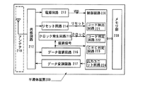
本実施例では、本発明の半導体装置を非接触でデータの入出力が可能である半導体装置に適用した例に関して図面を参照して説明する。なお、非接触でデータの入出力が可能である半導体装置は利用の形態によっては、RFID(Radio Frequency Identification)、IDタグ、ICタグ、ICチップ、RFタグ(Radio Frequency)、無線タグ、電子タグまたは無線チップともよばれる。
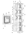
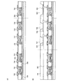
703 絶縁層
705 ゲート絶縁層
716 導電層
734 絶縁層
739 絶縁層
744 薄膜トランジスタ
745 薄膜トランジスタ
749 絶縁層
750 絶縁膜
751 絶縁層
752 導電膜
757 導電層
762 絶縁膜
763 導電膜
764 導電層
765 導電膜
766 絶縁膜
771 導電膜
772 絶縁膜
778 基板
786 導電層
787 層
789 記憶素子部
790 記憶素子部
791 素子形成層
Claims (6)
- 第1の基板上に、剥離層を形成し、
前記剥離層上に、第1の絶縁層を形成し、
前記第1の絶縁層上に、第1乃至第3の半導体層を形成し、
前記第1乃至第3の半導体層上に、第2の絶縁層を形成し、
前記第1の半導体層及び前記第2の半導体層に、一導電型を付与する第1の不純物を添加し、
前記第2の絶縁層上に、前記第2の半導体層と重なる領域を有する第1の電極と、前記第3の半導体層と重なる領域を有する第2の電極と、を形成し、
前記第1の半導体層及び前記第3の半導体層に、前記一導電型と逆の導電型を付与する第2の不純物を添加し、
前記第2の絶縁層、前記第1の電極、前記第2の電極上に、第3の絶縁層を形成し、
前記第3の絶縁層上に、導電層及び記憶素子部を形成し、
前記導電層及び前記記憶素子部上に、樹脂を有する層を形成し、
前記第1の基板を前記第1の絶縁層から剥離し、
第2の基板の一方の表面と前記第1の絶縁層とを接着する半導体装置の作製方法であって、
前記第1の半導体層は、前記第2の不純物が添加された第1の領域と、前記第2の不純物が添加されていない第2の領域を有し、
前記第1の領域又は前記第2の領域は、前記記憶素子部と電気的に接続され、
前記導電層の膜厚に対する、前記樹脂を有する層の前記導電層と重ならない領域の膜厚の比は、1.2以上であることを特徴とする半導体装置の作製方法。 - 請求項1において、
前記第2の基板の膜厚は2μm以上20μm以下であり、
前記第2の基板の他方の表面には、支持体が設けられていることを特徴とする半導体装置の作製方法。 - 請求項1又は2において、
前記第1の半導体層は、前記記憶素子部の少なくとも一部と重なる領域を有することを特徴とする半導体装置の作製方法。 - 請求項1乃至3のいずれか一項において、
前記第2の基板の表面は、二酸化珪素、インジウム錫酸化物、又は炭素を主成分とする材料によりコーティングされていることを特徴とする半導体装置の作製方法。 - 請求項1乃至4のいずれか一項において、
前記樹脂を有する層は、エポキシ樹脂を有することを特徴とする半導体装置の作製方法。 - 請求項1乃至5のいずれか一項において、
前記第2の基板は、ポリプロピレン、ポリエステル、ビニル、ポリフッ化ビニル若しくは塩化ビニルを有するフィルム、繊維質材料を有する紙、又は基材フィルムと接着性合成樹脂フィルムを有する積層フィルムであることを特徴とする半導体装置の作製方法。
Priority Applications (8)
| Application Number | Priority Date | Filing Date | Title |
|---|---|---|---|
| JP2006175611A JP5204959B2 (ja) | 2006-06-26 | 2006-06-26 | 半導体装置の作製方法 |
| US11/812,813 US7851886B2 (en) | 2006-06-26 | 2007-06-21 | Semiconductor device and manufacturing method of semiconductor device |
| TW096122935A TWI407508B (zh) | 2006-06-26 | 2007-06-25 | 半導體裝置及半導體裝置的製造方法 |
| KR1020070062172A KR101517525B1 (ko) | 2006-06-26 | 2007-06-25 | 반도체장치 및 반도체장치 제조방법 |
| US12/854,060 US8039353B2 (en) | 2006-06-26 | 2010-08-10 | Semiconductor device and manufacturing method of semiconductor device |
| US13/271,469 US8432018B2 (en) | 2006-06-26 | 2011-10-12 | Semiconductor device and manufacturing method of semiconductor device |
| US13/865,365 US8648439B2 (en) | 2006-06-26 | 2013-04-18 | Semiconductor device and manufacturing method of semiconductor device |
| KR1020130073305A KR101517943B1 (ko) | 2006-06-26 | 2013-06-25 | 반도체장치 및 반도체장치 제조방법 |
Applications Claiming Priority (1)
| Application Number | Priority Date | Filing Date | Title |
|---|---|---|---|
| JP2006175611A JP5204959B2 (ja) | 2006-06-26 | 2006-06-26 | 半導体装置の作製方法 |
Publications (3)
| Publication Number | Publication Date |
|---|---|
| JP2008004893A JP2008004893A (ja) | 2008-01-10 |
| JP2008004893A5 JP2008004893A5 (ja) | 2009-07-30 |
| JP5204959B2 true JP5204959B2 (ja) | 2013-06-05 |
Family
ID=38872782
Family Applications (1)
| Application Number | Title | Priority Date | Filing Date |
|---|---|---|---|
| JP2006175611A Expired - Fee Related JP5204959B2 (ja) | 2006-06-26 | 2006-06-26 | 半導体装置の作製方法 |
Country Status (4)
| Country | Link |
|---|---|
| US (4) | US7851886B2 (ja) |
| JP (1) | JP5204959B2 (ja) |
| KR (2) | KR101517525B1 (ja) |
| TW (1) | TWI407508B (ja) |
Families Citing this family (25)
| Publication number | Priority date | Publication date | Assignee | Title |
|---|---|---|---|---|
| US6850080B2 (en) * | 2001-03-19 | 2005-02-01 | Semiconductor Energy Laboratory Co., Ltd. | Inspection method and inspection apparatus |
| JPWO2006085466A1 (ja) * | 2005-02-14 | 2008-06-26 | 松下電器産業株式会社 | アンテナ内蔵半導体メモリモジュール |
| US20070183184A1 (en) * | 2006-02-03 | 2007-08-09 | Semiconductor Energy Laboratory Ltd. | Apparatus and method for manufacturing semiconductor device |
| JP5029605B2 (ja) * | 2006-04-03 | 2012-09-19 | パナソニック株式会社 | アンテナ内蔵半導体メモリモジュール |
| JP5204959B2 (ja) | 2006-06-26 | 2013-06-05 | 株式会社半導体エネルギー研究所 | 半導体装置の作製方法 |
| KR101350207B1 (ko) * | 2006-06-26 | 2014-01-13 | 가부시키가이샤 한도오따이 에네루기 켄큐쇼 | 반도체 장치를 포함하는 용지 및 그 제조 방법 |
| WO2009131132A1 (en) * | 2008-04-25 | 2009-10-29 | Semiconductor Energy Laboratory Co., Ltd. | Semiconductor device and method for manufacturing the same |
| WO2010032602A1 (en) | 2008-09-18 | 2010-03-25 | Semiconductor Energy Laboratory Co., Ltd. | Semiconductor device |
| US8441007B2 (en) * | 2008-12-25 | 2013-05-14 | Semiconductor Energy Laboratory Co., Ltd. | Display device and manufacturing method thereof |
| KR101481399B1 (ko) | 2009-12-18 | 2015-01-14 | 가부시키가이샤 한도오따이 에네루기 켄큐쇼 | 반도체 장치 |
| KR101823500B1 (ko) * | 2011-07-11 | 2018-01-31 | 삼성전자주식회사 | 상변화 메모리 장치의 제조 방법 |
| TWI453677B (zh) * | 2011-12-01 | 2014-09-21 | Mutual Pak Technology Co Ltd | 射頻識別標籤與具有其之衣物 |
| US8763912B1 (en) * | 2013-03-29 | 2014-07-01 | Identive Group, Inc. | Dual interface module and dual interface card having a dual interface module |
| US20150138699A1 (en) | 2013-11-15 | 2015-05-21 | Semiconductor Energy Laboratory Co., Ltd. | Electronic device |
| DE102013113283A1 (de) | 2013-11-29 | 2015-06-03 | Leonhard Kurz Stiftung & Co. Kg | Mehrschichtkörper und Verfahren zu dessen Herstellung |
| US9184143B2 (en) * | 2013-12-05 | 2015-11-10 | Taiwan Semiconductor Manufacturing Company Ltd. | Semiconductor device with bump adjustment and manufacturing method thereof |
| JP6065848B2 (ja) * | 2014-01-07 | 2017-01-25 | 株式会社Sumco | 半導体エピタキシャルウェーハの製造方法、半導体エピタキシャルウェーハ、および固体撮像素子の製造方法 |
| US10586954B2 (en) | 2014-05-23 | 2020-03-10 | Semiconductor Energy Laboratory Co., Ltd. | Electronic device including secondary battery |
| JP6419132B2 (ja) * | 2016-11-22 | 2018-11-07 | 東洋アルミエコープロダクツ株式会社 | パルプモールド構造体の製造方法及びパルプモールド構造体 |
| WO2019048981A1 (ja) | 2017-09-06 | 2019-03-14 | 株式会社半導体エネルギー研究所 | 半導体装置、バッテリーユニット、バッテリーモジュール |
| CN110082976B (zh) * | 2019-05-14 | 2022-08-02 | 上海天马微电子有限公司 | 显示模组和显示装置 |
| IL292568A (en) * | 2020-02-26 | 2022-06-01 | Showa Denko Kk | A dry etching method, a semiconductor element manufacturing method, and a cleaning method |
| KR102308784B1 (ko) * | 2020-02-28 | 2021-10-01 | 한양대학교 산학협력단 | 텔루륨 산화물 및 이를 채널층으로 구비하는 박막트랜지스터 |
| US11267629B2 (en) | 2020-07-02 | 2022-03-08 | Universal Trim Supply Co., Ltd. | Storage bag with easy flipping feature |
| US20260040600A1 (en) * | 2022-08-11 | 2026-02-05 | POSTECH Research and Business Development Foundation | Semiconductor containing amorphous tellurium oxide, thin film transistor including same, and fabrication method therefor |
Family Cites Families (50)
| Publication number | Priority date | Publication date | Assignee | Title |
|---|---|---|---|---|
| US5599046A (en) | 1994-06-22 | 1997-02-04 | Scientific Games Inc. | Lottery ticket structure with circuit elements |
| DE69739376D1 (de) * | 1996-08-27 | 2009-06-04 | Seiko Epson Corp | Ablösungsverfahren und Verfahren zum Übertragen eines Dünnfilm-Bauelements |
| US20050280155A1 (en) * | 2004-06-21 | 2005-12-22 | Sang-Yun Lee | Semiconductor bonding and layer transfer method |
| NL1008929C2 (nl) | 1998-04-20 | 1999-10-21 | Vhp Ugchelen Bv | Uit papier vervaardigd substraat voorzien van een geïntegreerde schakeling. |
| DE59911151D1 (de) | 1998-07-27 | 2004-12-30 | Joergen Brosow | Sicherheitspapier sowie verfahren und vorrichtung zur prüfung der echtheit darauf aufgezeichneter urkunden |
| JP4350253B2 (ja) | 2000-02-18 | 2009-10-21 | 株式会社日立製作所 | 電子回路チップ内蔵物の製造方法 |
| JP3625196B2 (ja) * | 2000-12-28 | 2005-03-02 | セイコーエプソン株式会社 | Rfidタグの形成方法、rfidタグの形成装置、スピーカの形成方法、およびスピーカの形成装置 |
| JP2002298118A (ja) | 2001-04-02 | 2002-10-11 | Dainippon Printing Co Ltd | 非接触方式のタグ部材が漉き込まれてなる用紙 |
| JP3925101B2 (ja) | 2001-04-19 | 2007-06-06 | 特種製紙株式会社 | 偽造防止用シート状物の製造方法 |
| JP4244120B2 (ja) * | 2001-06-20 | 2009-03-25 | 株式会社半導体エネルギー研究所 | 発光装置及びその作製方法 |
| US7211828B2 (en) | 2001-06-20 | 2007-05-01 | Semiconductor Energy Laboratory Co., Ltd. | Light emitting device and electronic apparatus |
| TW548860B (en) | 2001-06-20 | 2003-08-21 | Semiconductor Energy Lab | Light emitting device and method of manufacturing the same |
| JP4823705B2 (ja) * | 2003-02-24 | 2011-11-24 | 株式会社半導体エネルギー研究所 | 薄膜集積回路の作製方法及びicラベルの作製方法 |
| US7973313B2 (en) | 2003-02-24 | 2011-07-05 | Semiconductor Energy Laboratory Co., Ltd. | Thin film integrated circuit device, IC label, container comprising the thin film integrated circuit, manufacturing method of the thin film integrated circuit device, manufacturing method of the container, and management method of product having the container |
| US8999736B2 (en) * | 2003-07-04 | 2015-04-07 | Epistar Corporation | Optoelectronic system |
| US7566001B2 (en) * | 2003-08-29 | 2009-07-28 | Semiconductor Energy Laboratory Co., Ltd. | IC card |
| US7508305B2 (en) | 2003-12-26 | 2009-03-24 | Semiconductor Energy Laboratory Co., Ltd. | Packing material, tag, certificate, paper money, and securities |
| US7975926B2 (en) | 2003-12-26 | 2011-07-12 | Semiconductor Energy Laboratory Co., Ltd. | Paper money, coin, valuable instrument, certificates, tag, label, card, packing containers, documents, respectively installed with integrated circuit |
| TWI457835B (zh) * | 2004-02-04 | 2014-10-21 | Semiconductor Energy Lab | 攜帶薄膜積體電路的物品 |
| JP2005259984A (ja) * | 2004-03-11 | 2005-09-22 | Seiko Epson Corp | 転写方法、半導体装置の製造方法及び電子機器 |
| JP4865248B2 (ja) * | 2004-04-02 | 2012-02-01 | 株式会社半導体エネルギー研究所 | 半導体装置 |
| WO2005096380A1 (en) | 2004-04-02 | 2005-10-13 | Semiconductor Energy Laboratory Co., Ltd. | Semiconductor device and driving method of the same |
| DE102004018081A1 (de) | 2004-04-08 | 2005-10-27 | Giesecke & Devrient Gmbh | Sicherheitspapier |
| US8123896B2 (en) | 2004-06-02 | 2012-02-28 | Semiconductor Energy Laboratory Co., Ltd. | Laminating system |
| WO2005121908A1 (en) | 2004-06-14 | 2005-12-22 | Semiconductor Energy Laboratory Co., Ltd. | Copy machine with copy control function, scanner and facsimile, and piece of paper and film each installed with semiconductor device |
| KR101139713B1 (ko) | 2004-06-24 | 2012-04-26 | 가부시키가이샤 한도오따이 에네루기 켄큐쇼 | 박막 집적 회로를 제조하는 방법 |
| JP4912627B2 (ja) * | 2004-06-24 | 2012-04-11 | 株式会社半導体エネルギー研究所 | 薄膜集積回路の作製方法 |
| JP5041681B2 (ja) | 2004-06-29 | 2012-10-03 | 株式会社半導体エネルギー研究所 | 半導体装置の作製方法 |
| US7452786B2 (en) * | 2004-06-29 | 2008-11-18 | Semiconductor Energy Laboratory Co., Ltd. | Method for manufacturing thin film integrated circuit, and element substrate |
| US7591863B2 (en) | 2004-07-16 | 2009-09-22 | Semiconductor Energy Laboratory Co., Ltd. | Laminating system, IC sheet, roll of IC sheet, and method for manufacturing IC chip |
| JP4749062B2 (ja) | 2004-07-16 | 2011-08-17 | 株式会社半導体エネルギー研究所 | 薄膜集積回路を封止する装置及びicチップの作製方法 |
| US7259106B2 (en) * | 2004-09-10 | 2007-08-21 | Versatilis Llc | Method of making a microelectronic and/or optoelectronic circuitry sheet |
| JP4801337B2 (ja) | 2004-09-21 | 2011-10-26 | 株式会社半導体エネルギー研究所 | 半導体装置の作製方法 |
| JP5072210B2 (ja) | 2004-10-05 | 2012-11-14 | 株式会社半導体エネルギー研究所 | 半導体装置の作製方法 |
| US7935958B2 (en) | 2004-10-22 | 2011-05-03 | Semiconductor Energy Laboratory Co., Ltd. | Semiconductor device |
| JP2006148088A (ja) * | 2004-10-22 | 2006-06-08 | Semiconductor Energy Lab Co Ltd | 半導体装置 |
| JP2006165535A (ja) * | 2004-11-11 | 2006-06-22 | Semiconductor Energy Lab Co Ltd | 半導体装置 |
| US7816721B2 (en) | 2004-11-11 | 2010-10-19 | Semiconductor Energy Laboratory Co., Ltd. | Transmission/reception semiconductor device with memory element and antenna on same side of conductive adhesive |
| KR101169262B1 (ko) * | 2004-12-03 | 2012-08-02 | 가부시키가이샤 한도오따이 에네루기 켄큐쇼 | 반도체 장치 |
| US7482248B2 (en) * | 2004-12-03 | 2009-01-27 | Semiconductor Energy Laboratory Co., Ltd. | Manufacturing method of semiconductor device |
| KR100574521B1 (ko) * | 2004-12-14 | 2006-04-27 | 삼성전자주식회사 | 화상형성장치 |
| US7449372B2 (en) * | 2004-12-17 | 2008-11-11 | Semiconductor Energy Laboratory Co., Ltd. | Manufacturing method of substrate having conductive layer and manufacturing method of semiconductor device |
| FR2881252A1 (fr) | 2005-01-24 | 2006-07-28 | Ask Sa | Dispositif d'idenfication radiofrequence resistant aux milieux et son procede de fabrication |
| US7466233B2 (en) | 2005-05-04 | 2008-12-16 | Adalis Corporation | Substrates including tape and radio frequency identification devices, and methods and apparatus for making the same |
| US7566971B2 (en) * | 2005-05-27 | 2009-07-28 | Semiconductor Energy Laboratory Co., Ltd. | Semiconductor device and manufacturing method thereof |
| US7297613B1 (en) * | 2005-06-09 | 2007-11-20 | The United States Of America As Represented By The National Security Agency | Method of fabricating and integrating high quality decoupling capacitors |
| US7166520B1 (en) * | 2005-08-08 | 2007-01-23 | Silicon Genesis Corporation | Thin handle substrate method and structure for fabricating devices using one or more films provided by a layer transfer process |
| US20070083381A1 (en) | 2005-10-12 | 2007-04-12 | David Farrell | Method and system for creating receipt on paper with embedded RFID tags therein |
| KR101350207B1 (ko) | 2006-06-26 | 2014-01-13 | 가부시키가이샤 한도오따이 에네루기 켄큐쇼 | 반도체 장치를 포함하는 용지 및 그 제조 방법 |
| JP5204959B2 (ja) * | 2006-06-26 | 2013-06-05 | 株式会社半導体エネルギー研究所 | 半導体装置の作製方法 |
-
2006
- 2006-06-26 JP JP2006175611A patent/JP5204959B2/ja not_active Expired - Fee Related
-
2007
- 2007-06-21 US US11/812,813 patent/US7851886B2/en not_active Expired - Fee Related
- 2007-06-25 TW TW096122935A patent/TWI407508B/zh not_active IP Right Cessation
- 2007-06-25 KR KR1020070062172A patent/KR101517525B1/ko not_active Expired - Fee Related
-
2010
- 2010-08-10 US US12/854,060 patent/US8039353B2/en not_active Expired - Fee Related
-
2011
- 2011-10-12 US US13/271,469 patent/US8432018B2/en not_active Expired - Fee Related
-
2013
- 2013-04-18 US US13/865,365 patent/US8648439B2/en not_active Expired - Fee Related
- 2013-06-25 KR KR1020130073305A patent/KR101517943B1/ko not_active Expired - Fee Related
Also Published As
| Publication number | Publication date |
|---|---|
| JP2008004893A (ja) | 2008-01-10 |
| US7851886B2 (en) | 2010-12-14 |
| US8648439B2 (en) | 2014-02-11 |
| KR20130083880A (ko) | 2013-07-23 |
| US20110039373A1 (en) | 2011-02-17 |
| US8432018B2 (en) | 2013-04-30 |
| KR20070122395A (ko) | 2007-12-31 |
| KR101517525B1 (ko) | 2015-05-04 |
| US20120080810A1 (en) | 2012-04-05 |
| US20130228885A1 (en) | 2013-09-05 |
| US20070296037A1 (en) | 2007-12-27 |
| US8039353B2 (en) | 2011-10-18 |
| KR101517943B1 (ko) | 2015-05-06 |
| TW200814191A (en) | 2008-03-16 |
| TWI407508B (zh) | 2013-09-01 |
Similar Documents
| Publication | Publication Date | Title |
|---|---|---|
| JP5204959B2 (ja) | 半導体装置の作製方法 | |
| US8357567B2 (en) | Manufacturing method of semiconductor device | |
| US8295104B2 (en) | Semiconductor device | |
| US8227851B2 (en) | Semiconductor device | |
| JP5475947B2 (ja) | 紙及び半導体装置 | |
| JP5063066B2 (ja) | 半導体装置の作製方法 | |
| JP4704959B2 (ja) | 商品の管理方法および危険物の管理方法 | |
| JP5297584B2 (ja) | 半導体装置、半導体装置を用いた温度センサー及び半導体装置の作製方法 | |
| JP4954537B2 (ja) | 半導体装置 | |
| JP2007043121A (ja) | 半導体装置の作製方法 | |
| JP4974621B2 (ja) | 半導体装置及びその作製方法 | |
| JP2006179882A (ja) | 半導体装置およびその作製方法 |
Legal Events
| Date | Code | Title | Description |
|---|---|---|---|
| A521 | Request for written amendment filed |
Free format text: JAPANESE INTERMEDIATE CODE: A523 Effective date: 20090612 |
|
| A621 | Written request for application examination |
Free format text: JAPANESE INTERMEDIATE CODE: A621 Effective date: 20090612 |
|
| A131 | Notification of reasons for refusal |
Free format text: JAPANESE INTERMEDIATE CODE: A131 Effective date: 20120424 |
|
| A977 | Report on retrieval |
Free format text: JAPANESE INTERMEDIATE CODE: A971007 Effective date: 20120426 |
|
| A521 | Request for written amendment filed |
Free format text: JAPANESE INTERMEDIATE CODE: A523 Effective date: 20120621 |
|
| A131 | Notification of reasons for refusal |
Free format text: JAPANESE INTERMEDIATE CODE: A131 Effective date: 20121225 |
|
| A521 | Request for written amendment filed |
Free format text: JAPANESE INTERMEDIATE CODE: A523 Effective date: 20130124 |
|
| TRDD | Decision of grant or rejection written | ||
| A01 | Written decision to grant a patent or to grant a registration (utility model) |
Free format text: JAPANESE INTERMEDIATE CODE: A01 Effective date: 20130212 |
|
| A61 | First payment of annual fees (during grant procedure) |
Free format text: JAPANESE INTERMEDIATE CODE: A61 Effective date: 20130218 |
|
| R150 | Certificate of patent or registration of utility model |
Ref document number: 5204959 Country of ref document: JP Free format text: JAPANESE INTERMEDIATE CODE: R150 |
|
| FPAY | Renewal fee payment (event date is renewal date of database) |
Free format text: PAYMENT UNTIL: 20160222 Year of fee payment: 3 |
|
| FPAY | Renewal fee payment (event date is renewal date of database) |
Free format text: PAYMENT UNTIL: 20160222 Year of fee payment: 3 |
|
| R250 | Receipt of annual fees |
Free format text: JAPANESE INTERMEDIATE CODE: R250 |
|
| R250 | Receipt of annual fees |
Free format text: JAPANESE INTERMEDIATE CODE: R250 |
|
| R250 | Receipt of annual fees |
Free format text: JAPANESE INTERMEDIATE CODE: R250 |
|
| R250 | Receipt of annual fees |
Free format text: JAPANESE INTERMEDIATE CODE: R250 |
|
| R250 | Receipt of annual fees |
Free format text: JAPANESE INTERMEDIATE CODE: R250 |
|
| R250 | Receipt of annual fees |
Free format text: JAPANESE INTERMEDIATE CODE: R250 |
|
| LAPS | Cancellation because of no payment of annual fees |