JP4912627B2 - 薄膜集積回路の作製方法 - Google Patents
薄膜集積回路の作製方法 Download PDFInfo
- Publication number
- JP4912627B2 JP4912627B2 JP2005185380A JP2005185380A JP4912627B2 JP 4912627 B2 JP4912627 B2 JP 4912627B2 JP 2005185380 A JP2005185380 A JP 2005185380A JP 2005185380 A JP2005185380 A JP 2005185380A JP 4912627 B2 JP4912627 B2 JP 4912627B2
- Authority
- JP
- Japan
- Prior art keywords
- region
- layer
- substrate
- insulating film
- thin film
- Prior art date
- Legal status (The legal status is an assumption and is not a legal conclusion. Google has not performed a legal analysis and makes no representation as to the accuracy of the status listed.)
- Expired - Fee Related
Links
Images


Description
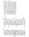
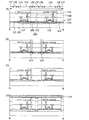
102 剥離層
103 剥離層
104 剥離層
105 絶縁膜
106 素子群
107 絶縁膜
108 絶縁膜
109 薄膜集積回路
110 導電層
111 絶縁膜
112 開口部
113 開口部
114 基体
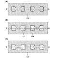
115 第1の領域
116 第2の領域
117 トランジスタ
118 トランジスタ
119 絶縁膜
121 剥離層
122 剥離層
123 開口部
124 開口部
125 剥離層
126 開口部
131 剥離層
132 開口部
135 第3の領域
136 第4の領域
137 第5の領域
140 基体
Claims (9)
- 絶縁表面を有する基板上の第1の領域と第2の領域に剥離層を形成し、
前記第2の領域の前記剥離層を除去し、
前記第1の領域の前記剥離層上と前記第2の領域の前記基板上に、絶縁膜を形成し、
前記第1の領域の前記絶縁膜上に、複数の素子と導電層を形成し、
前記第1の領域の前記絶縁膜に、前記剥離層が露出される開口部を形成し、
前記第1の領域の前記開口部にエッチング剤を導入して、前記剥離層を除去することを特徴とする薄膜集積回路の作製方法。 - 絶縁表面を有する基板上の第1の領域と第2の領域に剥離層を形成し、
前記第1の領域の前記剥離層を選択的に除去し、
前記第2の領域の前記剥離層を除去し、
前記第1の領域の前記基板及び前記剥離層上と前記第2の領域の前記基板上に、絶縁膜を形成し、
前記第1の領域の前記絶縁膜上に、複数の素子と導電層を形成し、
前記第1の領域の前記絶縁膜に、前記剥離層が露出される開口部を形成し、
前記第1の領域の前記開口部にエッチング剤を導入して、前記剥離層を除去し、
前記第1の領域の前記剥離層を選択的に除去する工程では、前記第1の領域に含まれ前記複数の素子と前記導電層が設けられた第3の領域の前記剥離層は除去せず、前記第1の領域に含まれ前記開口部が設けられた第4の領域の前記剥離層は除去せず、前記第1の領域に含まれ前記第3の領域と前記第4の領域を除く第5の領域の前記剥離層を除去することを特徴とする薄膜集積回路の作製方法。 - 絶縁表面を有する基板上の第1の領域と第2の領域に剥離層を形成し、
前記第1の領域の前記剥離層を選択的に除去し、
前記第2の領域の前記剥離層を除去し、
前記第1の領域の前記基板及び前記剥離層上と前記第2の領域の前記基板上に、絶縁膜を形成し、
前記第1の領域の前記絶縁膜上に、複数の素子と導電層を形成し、
前記第1の領域の前記絶縁膜に、前記剥離層が露出される開口部を形成し、
前記第1の領域の前記開口部にエッチング剤を導入して、前記剥離層を除去し、
前記第1の領域の前記剥離層を選択的に除去する工程では、前記第1の領域に含まれ前記複数の素子と前記導電層が設けられた第3の領域の前記剥離層は除去せず、前記第1の領域に含まれ前記開口部が設けられた第4の領域の前記剥離層は除去せず、前記第1の領域に含まれ前記第3の領域と前記第4の領域を除く第5の領域の前記剥離層を選択的に除去することを特徴とする薄膜集積回路の作製方法。 - 絶縁表面を有する基板上の第1の領域と第2の領域に剥離層を形成し、
前記第1の領域の前記剥離層を選択的に除去し、
前記第2の領域の前記剥離層を除去し、
前記第1の領域の前記基板及び前記剥離層上と前記第2の領域の前記基板上に、絶縁膜を形成し、
前記第1の領域の前記絶縁膜上に、複数の素子と導電層を形成し、
前記第1の領域の前記絶縁膜に、前記剥離層が露出される開口部を形成し、
前記第1の領域の前記開口部にエッチング剤を導入して、前記剥離層を除去し、
前記第1の領域の前記剥離層を選択的に除去する工程では、前記第1の領域に含まれ前記複数の素子と前記導電層が設けられた第3の領域の前記剥離層を選択的に除去し、前記第1の領域に含まれ前記開口部が設けられた第4の領域の前記剥離層を除去しないことを特徴とする薄膜集積回路の作製方法。 - 請求項1乃至請求項4のいずれか一項において、
前記第2の領域の前記剥離層を選択的に除去することを特徴とする薄膜集積回路の作製方法。 - 請求項1において、
前記絶縁膜は、前記第1の領域の前記剥離層と前記第2の領域の前記基板に接するように、形成されることを特徴とする薄膜集積回路の作製方法。 - 請求項2乃至請求項4のいずれか一項において、
前記絶縁膜は、前記第1の領域の前記基板及び前記剥離層と、前記第2の領域の前記基板に接するように、形成されることを特徴とする薄膜集積回路の作製方法。 - 請求項1乃至請求項7のいずれか一項において、
前記エッチング剤は、フッ化ハロゲンを含む気体又は液体であることを特徴とする薄膜集積回路の作製方法。 - 請求項1乃至請求項8のいずれか一項において、
前記導電層は、アンテナとして機能することを特徴とする薄膜集積回路の作製方法。
Priority Applications (1)
| Application Number | Priority Date | Filing Date | Title |
|---|---|---|---|
| JP2005185380A JP4912627B2 (ja) | 2004-06-24 | 2005-06-24 | 薄膜集積回路の作製方法 |
Applications Claiming Priority (3)
| Application Number | Priority Date | Filing Date | Title |
|---|---|---|---|
| JP2004186543 | 2004-06-24 | ||
| JP2004186543 | 2004-06-24 | ||
| JP2005185380A JP4912627B2 (ja) | 2004-06-24 | 2005-06-24 | 薄膜集積回路の作製方法 |
Publications (3)
| Publication Number | Publication Date |
|---|---|
| JP2006041502A JP2006041502A (ja) | 2006-02-09 |
| JP2006041502A5 JP2006041502A5 (ja) | 2008-05-15 |
| JP4912627B2 true JP4912627B2 (ja) | 2012-04-11 |
Family
ID=35906104
Family Applications (1)
| Application Number | Title | Priority Date | Filing Date |
|---|---|---|---|
| JP2005185380A Expired - Fee Related JP4912627B2 (ja) | 2004-06-24 | 2005-06-24 | 薄膜集積回路の作製方法 |
Country Status (1)
| Country | Link |
|---|---|
| JP (1) | JP4912627B2 (ja) |
Families Citing this family (4)
| Publication number | Priority date | Publication date | Assignee | Title |
|---|---|---|---|---|
| JP5204959B2 (ja) * | 2006-06-26 | 2013-06-05 | 株式会社半導体エネルギー研究所 | 半導体装置の作製方法 |
| JP5264016B2 (ja) * | 2006-06-30 | 2013-08-14 | 株式会社半導体エネルギー研究所 | 半導体装置の作製方法 |
| CN103956336B (zh) * | 2006-09-20 | 2019-08-16 | 伊利诺伊大学评议会 | 用于制造可转移半导体结构、器件和器件构件的松脱策略 |
| KR20200112851A (ko) * | 2017-12-22 | 2020-10-05 | 보드 오브 리전츠, 더 유니버시티 오브 텍사스 시스템 | 나노스케일 정렬된 삼차원 적층 집적 회로 |
Family Cites Families (2)
| Publication number | Priority date | Publication date | Assignee | Title |
|---|---|---|---|---|
| JP4748859B2 (ja) * | 2000-01-17 | 2011-08-17 | 株式会社半導体エネルギー研究所 | 発光装置の作製方法 |
| TW586231B (en) * | 2001-07-24 | 2004-05-01 | Seiko Epson Corp | Transfer method, methods of manufacturing thin film devices and integrated circuits, circuit board and manufacturing method thereof, electro-optical apparatus and manufacturing method thereof, manufacturing methods of IC card and electronic appliance |
-
2005
- 2005-06-24 JP JP2005185380A patent/JP4912627B2/ja not_active Expired - Fee Related
Also Published As
| Publication number | Publication date |
|---|---|
| JP2006041502A (ja) | 2006-02-09 |
Similar Documents
| Publication | Publication Date | Title |
|---|---|---|
| US9536755B2 (en) | Laminating system | |
| US7591863B2 (en) | Laminating system, IC sheet, roll of IC sheet, and method for manufacturing IC chip | |
| US7879687B2 (en) | Manufacturing method of semiconductor device | |
| US7476575B2 (en) | Method for manufacturing thin film integrated circuit | |
| JP2014160826A (ja) | 半導体装置 | |
| JP2008141167A (ja) | 導電層及び導電層を有する基板の形成方法、並びに半導体装置の作製方法 | |
| JP4749062B2 (ja) | 薄膜集積回路を封止する装置及びicチップの作製方法 | |
| JP4912627B2 (ja) | 薄膜集積回路の作製方法 | |
| EP1886355A1 (en) | Semiconductor device | |
| JP5025103B2 (ja) | Icチップの作製方法 | |
| JP5132135B2 (ja) | 半導体装置の作製方法 | |
| JP5084177B2 (ja) | 半導体装置 |
Legal Events
| Date | Code | Title | Description |
|---|---|---|---|
| A521 | Written amendment |
Free format text: JAPANESE INTERMEDIATE CODE: A523 Effective date: 20080331 |
|
| A621 | Written request for application examination |
Free format text: JAPANESE INTERMEDIATE CODE: A621 Effective date: 20080331 |
|
| A131 | Notification of reasons for refusal |
Free format text: JAPANESE INTERMEDIATE CODE: A131 Effective date: 20110920 |
|
| A521 | Written amendment |
Free format text: JAPANESE INTERMEDIATE CODE: A523 Effective date: 20110928 |
|
| TRDD | Decision of grant or rejection written | ||
| A01 | Written decision to grant a patent or to grant a registration (utility model) |
Free format text: JAPANESE INTERMEDIATE CODE: A01 Effective date: 20120117 |
|
| A01 | Written decision to grant a patent or to grant a registration (utility model) |
Free format text: JAPANESE INTERMEDIATE CODE: A01 |
|
| A61 | First payment of annual fees (during grant procedure) |
Free format text: JAPANESE INTERMEDIATE CODE: A61 Effective date: 20120118 |
|
| R150 | Certificate of patent or registration of utility model |
Free format text: JAPANESE INTERMEDIATE CODE: R150 |
|
| FPAY | Renewal fee payment (event date is renewal date of database) |
Free format text: PAYMENT UNTIL: 20150127 Year of fee payment: 3 |
|
| FPAY | Renewal fee payment (event date is renewal date of database) |
Free format text: PAYMENT UNTIL: 20150127 Year of fee payment: 3 |
|
| R250 | Receipt of annual fees |
Free format text: JAPANESE INTERMEDIATE CODE: R250 |
|
| R250 | Receipt of annual fees |
Free format text: JAPANESE INTERMEDIATE CODE: R250 |
|
| R250 | Receipt of annual fees |
Free format text: JAPANESE INTERMEDIATE CODE: R250 |
|
| LAPS | Cancellation because of no payment of annual fees |