JP4912627B2 - Method for manufacturing thin film integrated circuit - Google Patents
Method for manufacturing thin film integrated circuit Download PDFInfo
- Publication number
- JP4912627B2 JP4912627B2 JP2005185380A JP2005185380A JP4912627B2 JP 4912627 B2 JP4912627 B2 JP 4912627B2 JP 2005185380 A JP2005185380 A JP 2005185380A JP 2005185380 A JP2005185380 A JP 2005185380A JP 4912627 B2 JP4912627 B2 JP 4912627B2
- Authority
- JP
- Japan
- Prior art keywords
- region
- layer
- substrate
- insulating film
- thin film
- Prior art date
- Legal status (The legal status is an assumption and is not a legal conclusion. Google has not performed a legal analysis and makes no representation as to the accuracy of the status listed.)
- Expired - Fee Related
Links
Images


Description
本発明は、薄膜集積回路の作製方法に関する。 The present invention relates to a method for manufacturing a thin film integrated circuit.
近年、絶縁基板上に設けられた薄膜集積回路を転置する技術開発が進められている。このような技術として、例えば、薄膜集積回路と基板の間に剥離層を設けて、当該剥離層を、ハロゲンを含む気体を用いて除去することにより、薄膜集積回路を支持基板から分離し、その後転置する技術がある(例えば、特許文献1参照)。
上記の特許文献によると、基板の一表面に剥離層を形成し、当該剥離層上に薄膜集積回路を形成し、続いて剥離層を除去する。そうすると、薄膜集積回路は基板から剥離され、基板と薄膜集積回路の間には空間が生じる。その後、薄膜集積回路を基体に接着させるが、当該薄膜集積回路は数μm程度と薄く、また大変軽いものである。そのため、薄膜集積回路を基体に接着させる前に、当該薄膜集積回路が基板から飛散してしまうことがあった。そこで本発明は、薄膜集積回路の飛散を防止することを課題とする。また、剥離層を除去した後の薄膜集積回路の基体への転置を容易に行うことを課題とする。 According to the above patent document, a peeling layer is formed on one surface of a substrate, a thin film integrated circuit is formed on the peeling layer, and then the peeling layer is removed. Then, the thin film integrated circuit is separated from the substrate, and a space is generated between the substrate and the thin film integrated circuit. Thereafter, the thin film integrated circuit is bonded to the substrate. The thin film integrated circuit is as thin as several μm and is very light. Therefore, before the thin film integrated circuit is bonded to the substrate, the thin film integrated circuit may be scattered from the substrate. Thus, an object of the present invention is to prevent scattering of a thin film integrated circuit. It is another object of the present invention to easily transfer a thin film integrated circuit to a substrate after removing a peeling layer.
本発明は、基板の一表面に剥離層を形成した後に、当該剥離層を選択的に除去して、剥離層が設けられた第1の領域と、剥離層が設けられていない第2の領域を形成する。続いて、下地用の絶縁膜を全面に形成する。そうすると、絶縁膜は、第1の領域では剥離層に接し、第2の領域では基板に接する。 In the present invention, after the release layer is formed on one surface of the substrate, the release layer is selectively removed, and the first region where the release layer is provided and the second region where the release layer is not provided Form. Subsequently, a base insulating film is formed on the entire surface. Then, the insulating film is in contact with the release layer in the first region and in contact with the substrate in the second region.
次に、第1の領域の絶縁膜上に複数の素子とアンテナとして機能する導電層を含む薄膜集積回路を形成し、続いて開口部を形成し、その後開口部にエッチング剤を導入して剥離層を除去する。この際、剥離層が設けられていた第1の領域では、基板と絶縁膜の間に空間が生じるが、剥離層が設けられていない第2の領域では、基板と絶縁膜が密着したままである。 Next, a thin film integrated circuit including a plurality of elements and a conductive layer functioning as an antenna is formed over the insulating film in the first region, and then an opening is formed. Thereafter, an etching agent is introduced into the opening and then peeled off. Remove the layer. At this time, a space is generated between the substrate and the insulating film in the first region where the release layer is provided, but the substrate and the insulating film remain in close contact with each other in the second region where the release layer is not provided. is there.
このように、剥離層を除去した後も、基板と絶縁膜が密着した領域が設けられていることで、絶縁膜の上方に設けられた薄膜集積回路の飛散を防止することができる。また、基板と絶縁膜が密着した領域が設けられていることで、基板上に薄膜集積回路を保持することができ、当該薄膜集積回路の基体への転置を容易に行うことができる。 As described above, even after the peeling layer is removed, the region where the substrate and the insulating film are in close contact with each other is provided, so that scattering of the thin film integrated circuit provided above the insulating film can be prevented. Further, since the region where the substrate and the insulating film are in close contact with each other is provided, the thin film integrated circuit can be held on the substrate, and the thin film integrated circuit can be easily transferred to the base.
本発明の薄膜集積回路の作製方法は、絶縁表面を有する基板上の第1の領域と第2の領域に剥離層を形成する工程と、第2の領域の剥離層のみを除去する工程と、絶縁基板又は剥離層に接するように絶縁膜を形成する工程と、第1の領域の絶縁膜上に複数の素子とアンテナとして機能する導電層を形成する工程と、複数の素子と導電層が設けられた領域以外に開口部を選択的に形成して剥離層を露出させる工程と、開口部にエッチング剤を導入して剥離層を除去する工程とを有することを特徴とする。 The method for manufacturing a thin film integrated circuit of the present invention includes a step of forming a release layer in the first region and the second region on a substrate having an insulating surface, a step of removing only the release layer in the second region, A step of forming an insulating film in contact with the insulating substrate or the peeling layer; a step of forming a plurality of elements and a conductive layer functioning as an antenna over the insulating film in the first region; and a plurality of elements and a conductive layer provided. The method includes a step of selectively forming an opening other than the formed region to expose the release layer, and a step of introducing an etchant into the opening to remove the release layer.
本発明の薄膜集積回路の作製方法は、絶縁表面を有する基板上の第1の領域と第2の領域に剥離層を形成する工程と、第1の領域の剥離層を選択的に除去する工程と、第2の領域の剥離層を除去する工程と、絶縁基板又は剥離層に接するように絶縁膜を形成する工程と、第1の領域の絶縁膜上に複数の素子とアンテナとして機能する導電層を形成する工程と、複数の素子と導電層が設けられた第3の領域の周囲の第4の領域に開口部を選択的に形成して剥離層を露出させる工程と、開口部にエッチング剤を導入して剥離層を除去する工程とを有し、第1の領域の剥離層の選択的な除去の工程では、第1の領域が含む第3の領域と第4の領域以外の第5の領域の剥離層を除去し、第3の領域と第4の領域の剥離層を除去しないことを特徴とする。 A method for manufacturing a thin film integrated circuit according to the present invention includes a step of forming a release layer in a first region and a second region on a substrate having an insulating surface, and a step of selectively removing the release layer in the first region. A step of removing the peeling layer in the second region, a step of forming an insulating film so as to be in contact with the insulating substrate or the peeling layer, and a plurality of elements and a conductive material functioning as an antenna over the insulating film in the first region A step of forming a layer, a step of selectively forming an opening in a fourth region around a third region provided with a plurality of elements and a conductive layer, exposing a peeling layer, and etching in the opening And a step of removing the release layer by introducing an agent. In the step of selectively removing the release layer in the first region, the third region included in the first region and the third region other than the fourth region are included. The release layer in the region 5 is removed, and the release layer in the third region and the fourth region is not removed.
本発明の薄膜集積回路の作製方法は、絶縁表面を有する基板上の第1の領域と第2の領域に剥離層を形成する工程と、第1の領域の剥離層を選択的に除去する工程と、第2の領域の剥離層を除去する工程と、絶縁基板又は剥離層に接するように絶縁膜を形成する工程と、第1の領域の絶縁膜上に複数の素子とアンテナとして機能する導電層を形成する工程と、複数の素子と導電層が設けられた第3の領域と第3の領域の周囲の第5の領域以外の第4の領域に開口部を形成して剥離層を露出させる工程と、開口部にエッチング剤を導入して剥離層を除去する工程とを有し、第1の領域の剥離層の選択的な除去の工程では、第1の領域が含む第5の領域の剥離層を選択的に除去し、第3の領域と第4の領域の剥離層を除去しないことを特徴とする。 A method for manufacturing a thin film integrated circuit according to the present invention includes a step of forming a release layer in a first region and a second region on a substrate having an insulating surface, and a step of selectively removing the release layer in the first region. A step of removing the peeling layer in the second region, a step of forming an insulating film so as to be in contact with the insulating substrate or the peeling layer, and a plurality of elements and a conductive material functioning as an antenna over the insulating film in the first region Forming a layer, a third region provided with a plurality of elements and a conductive layer, and forming an opening in a fourth region other than the fifth region around the third region to expose the release layer And a step of removing the release layer by introducing an etching agent into the opening. In the step of selectively removing the release layer in the first region, the fifth region included in the first region The release layer is selectively removed, and the release layers in the third region and the fourth region are not removed.
本発明の薄膜集積回路の作製方法は、絶縁表面を有する基板上の第1の領域と第2の領域に剥離層を形成する工程と、第1の領域の剥離層を選択的に除去する工程と、第2の領域の剥離層を除去する工程と、絶縁基板又は剥離層に接するように絶縁膜を形成する工程と、第1の領域の絶縁膜上に複数の素子とアンテナとして機能する導電層を形成する工程と、複数の素子と導電層が設けられた第3の領域以外の第4の領域に開口部を選択的に形成して剥離層を露出させる工程と、開口部にエッチング剤を導入して剥離層を除去する工程とを有し、第1の領域の剥離層の選択的な除去の工程では、第1の領域が含む第3の領域の剥離層を選択的に除去し、第3の領域以外の剥離層を除去しないことを特徴とする。 A method for manufacturing a thin film integrated circuit according to the present invention includes a step of forming a release layer in a first region and a second region on a substrate having an insulating surface, and a step of selectively removing the release layer in the first region. A step of removing the peeling layer in the second region, a step of forming an insulating film so as to be in contact with the insulating substrate or the peeling layer, and a plurality of elements and a conductive material functioning as an antenna over the insulating film in the first region A step of forming a layer, a step of selectively forming an opening in a fourth region other than the third region provided with a plurality of elements and a conductive layer to expose the release layer, and an etching agent in the opening And removing the peeling layer by selectively removing the peeling layer in the third region included in the first region in the step of selectively removing the peeling layer in the first region. The release layer other than the third region is not removed.
上記工程を有する薄膜集積回路の作製方法において、第2の領域の剥離層を除去する工程を、第2の領域の剥離層を選択的に除去する工程に置換してもよい。また、エッチング剤はフッ化ハロゲンを含む気体又は液体であることを特徴とする。 In the method for manufacturing a thin film integrated circuit including the above steps, the step of removing the peeling layer in the second region may be replaced with a step of selectively removing the peeling layer in the second region. Further, the etching agent is a gas or a liquid containing halogen fluoride.
本発明は、剥離層を除去した後も、基板と絶縁膜が密着した領域を設けることで、当該絶縁膜の上方に設けられた薄膜集積回路の飛散を防止することができる。また、基板と絶縁膜が密着した領域を設けることで、基板上に薄膜集積回路を保持することができるため、当該薄膜集積回路の基体への転置を容易に行うことができる。 The present invention can prevent scattering of a thin film integrated circuit provided above the insulating film by providing a region where the substrate and the insulating film are in close contact with each other even after the peeling layer is removed. In addition, since the thin film integrated circuit can be held on the substrate by providing the region in which the substrate and the insulating film are in close contact with each other, the thin film integrated circuit can be easily transferred to the base.
また、本発明のように、基板上に薄膜集積回路が保持された状態であれば、当該基板をそのまま搬送することができるため、搬送手段を含む量産装置に用いることができる。例えば、ラミネート装置に、薄膜集積回路が保持された基板を搬送すれば、当該薄膜集積回路のラミネート処理を連続的に行うことができる。 Further, as long as the thin film integrated circuit is held on the substrate as in the present invention, the substrate can be transported as it is, so that it can be used for a mass production apparatus including a transporting unit. For example, when a substrate holding a thin film integrated circuit is conveyed to a laminating apparatus, the thin film integrated circuit can be continuously laminated.
また、上記の構成によると、薄膜集積回路を1つの単位として、第1の領域と第2の領域が作り分けられているため、任意の薄膜集積回路のみを基体に転置することができる。 Further, according to the above configuration, since the first region and the second region are separately formed using the thin film integrated circuit as one unit, only an arbitrary thin film integrated circuit can be transferred to the substrate.
また、薄膜集積回路を1つの単位として、第1の領域と第2の領域が作り分けられているため、剥離層を除去後、複数の薄膜集積回路の各々を分断する必要がない。つまり、薄膜集積回路を基体に転置した段階で、複数の薄膜集積回路の各々は分断された状態となる。 In addition, since the first region and the second region are separately formed using the thin film integrated circuit as one unit, it is not necessary to divide each of the plurality of thin film integrated circuits after removing the peeling layer. That is, at the stage where the thin film integrated circuit is transferred to the substrate, each of the plurality of thin film integrated circuits is in a divided state.
本発明の実施の形態について、図面を用いて詳細に説明する。但し、本発明は以下の説明に限定されず、本発明の趣旨及びその範囲から逸脱することなくその形態及び詳細を様々に変更し得ることは当業者であれば容易に理解される。従って、本発明は以下に示す実施の形態の記載内容に限定して解釈されるものではない。なお、以下に説明する本発明の構成において、同じものを指す符号は異なる図面間で共通して用いる。 Embodiments of the present invention will be described in detail with reference to the drawings. However, the present invention is not limited to the following description, and it is easily understood by those skilled in the art that modes and details can be variously changed without departing from the spirit and scope of the present invention. Therefore, the present invention should not be construed as being limited to the description of the embodiments below. Note that in the structures of the present invention described below, the same reference numerals are used in common in different drawings.
本発明の薄膜集積回路の作製方法について、4つに大別して、図面を参照して説明する。 A method for manufacturing a thin film integrated circuit according to the present invention is roughly divided into four methods and will be described with reference to the drawings.
まず、第1の作製方法について図1、2を参照して説明する。 First, the first manufacturing method will be described with reference to FIGS.
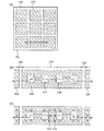
絶縁表面を有する基板101の一表面に剥離層を形成する。次に、剥離層を選択的に除去して、剥離層が設けられた第1の領域115と、剥離層を除去した第2の領域116を形成する(図1(A)の上面図参照)。剥離層が設けられた第1の領域115には、後に薄膜集積回路を形成する。剥離層を除去した第2の領域116には、薄膜集積回路を形成せず、後に形成する絶縁膜と基板101とが密着した領域となる。
A separation layer is formed over one surface of the
図1(A)に示す上面図では、第1の領域115(斜線の領域)は、第2の領域116に囲まれている。また、図1(A)に示す上面図では、第1の領域115は四角形状の領域である。なお、第1の領域115と第2の領域116の位置関係やその形状は特に制約されない。
In the top view illustrated in FIG. 1A, the first region 115 (shaded region) is surrounded by the
本発明では、薄膜集積回路を1つの単位として、第1の領域115と第2の領域116が作り分けられているため、任意の薄膜集積回路のみを基体に転置することができる。また、薄膜集積回路を1つの単位として、第1の領域115と第2の領域116が作り分けられているため、基体に転置する工程を経ると、複数の薄膜集積回路の各々は自動的に分断される。そのため、複数の薄膜集積回路を分断する工程を省略することができる。
In the present invention, since the
絶縁表面を有する基板101とは、ガラス基板、石英基板、プラスチック基板、アクリル等の可撓性を有する合成樹脂からなる樹脂基板、金属基板に相当する。また、剥離層は、珪素を含む層をスパッタリング法やプラズマCVD法等の公知の方法により形成する。珪素を含む層とは、非晶質半導体層、非晶質状態と結晶質状態とが混在したセミアモルファス半導体層、結晶質半導体層に相当する。
The
また、剥離層の選択的な除去は、フォトリソグラフィ法を用いて行うとよい。なお、上記の工程では、基板101の一表面の全面に剥離層を形成してから、選択的に剥離層を除去しているが、本発明はこの工程に制約されない。メタルマスク等のマスクを用いることで、予め、基板101上に剥離層を選択的に形成してもよい。
Further, the selective removal of the peeling layer is preferably performed using a photolithography method. Note that in the above process, a release layer is formed over the entire surface of one surface of the
続いて、以下の工程について、図1、2を用いて説明する。図1の上面図のA−Bは、図2の断面図のA−Bに対応する。 Subsequently, the following steps will be described with reference to FIGS. A-B in the top view of FIG. 1 corresponds to A-B in the cross-sectional view of FIG.
まず、基板101又は剥離層102〜104に接するように、下地用の絶縁膜105を形成する(図1(B)と図2(A)参照)。絶縁膜105は、第1の領域115では剥離層102〜104に接し、第2の領域116では基板101に接する。絶縁膜105は、プラズマCVD法やスパッタリング法等の公知の方法を用いて、酸化珪素、窒化珪素、酸化窒化珪素、窒化酸化珪素等からなる薄膜を形成する。
First, the
続いて、第1の領域115の絶縁膜105上に複数の素子を含む素子群106を形成する。素子群106は、例えば、薄膜トランジスタ、容量素子、抵抗素子、ダイオード等を1種又は複数種形成する。ここでは、素子群106として、2つのトランジスタ117、118を形成する。次に、素子群106を覆うように、絶縁膜107を形成し、絶縁膜107上に、絶縁膜108を形成する。続いて、絶縁膜108上に、導電層110を形成する。導電層110は、アンテナとして機能する。次に、導電層110上に、保護膜として機能する絶縁膜111を形成する。上記の工程を経て、素子群106と導電層110を含む薄膜集積回路109が完成する。なお図1(B)では、トランジスタ117、118が含む半導体層の上面図のみを示し、トランジスタ117、118上に設けられる導電層110の図示は省略している。
Subsequently, an
絶縁膜107、108、111は、有機材料又は無機材料により形成する。有機材料は、ポリイミド、アクリル、ポリアミド、エポキシ等を用いる。また、絶縁膜107、108、111は、シロキサンにより形成する。シロキサンは、珪素と酸素との結合で骨格構造が構成され、置換基に少なくとも水素を含む有機基(例えばアルキル基、芳香族炭化水素)が用いられる。又は、置換基としてフルオロ基を用いてもよい。又は、置換基として、少なくとも水素を含む有機基と、フルオロ基とを用いてもよい。また、無機材料には、酸化珪素、窒化珪素、酸化窒化珪素、窒化酸化珪素等を用いる。
The insulating
続いて、素子群106と導電層110が設けられた領域以外に、開口部112、113を選択的に形成して、剥離層102〜104を露出させる(図1(C)と図2(B)参照)。つまり、素子群106と導電層110が設けられた領域の外周に開口部を選択的に形成する。開口部は、マスクを利用したエッチング等によって形成する。図1(C)の上面図では、開口部は点線の四角で示す。
Subsequently, in addition to the region where the
なお、開口部は、上述したエッチングという方法以外に、レーザービームを照射することによって形成してもよい。 Note that the opening may be formed by irradiating a laser beam other than the above-described etching method.
続いて、開口部112、113に、剥離層102〜104を除去するエッチング剤を導入して、剥離層102〜104を除去する(図2(C)参照)。エッチング剤には、フッ化ハロゲンを含む気体又は液体を使用する。フッ化ハロゲンを含む気体としては、例えば三フッ化塩素(ClF3)を使用する。
Subsequently, an etching agent for removing the separation layers 102 to 104 is introduced into the
次に、素子群106と導電層110を含む薄膜集積回路109を基体114に接着させて、薄膜集積回路109を基板101から剥離する(図2(D)参照)。この際、剥離層102〜104が除去された部分は基体114に接着して基板101から完全に剥離され、基板101と絶縁膜105が密着した部分は基板101に保持されたままとなる。
Next, the thin film integrated
なお、本発明は上記の形態に制約されない。薄膜集積回路109を基体114に接着させる際、基板101と絶縁膜105が密着した部分も基体114に接着され、基板101から剥離することがある。
In addition, this invention is not restrict | limited to said form. When the thin film integrated
基体114には、プラスチック等からなる可撓性基板、両面テープなどを用いるとよい。可撓性基板には、熱硬化樹脂などの接着剤からなる接着面を設けていてもよい。また、基体114を用いずに、物品の表面に接着させてもよい。そうすれば、実装する物品の薄型化や軽量化に貢献することになる。
As the
上記の作製方法では、剥離層を選択的に形成することを特徴とする。上記特徴により、剥離層を除去した後も、絶縁膜105の一部が基板101に密着した状態にあるため、薄膜集積回路109を基板101上に保持することができ、薄膜集積回路109の飛散を防止することができる。
The above manufacturing method is characterized in that a release layer is selectively formed. With the above feature, after the separation layer is removed, part of the insulating
次に、第2の作製方法について、図3〜5を参照して説明する。 Next, a second manufacturing method will be described with reference to FIGS.
絶縁表面を有する基板101の一表面に剥離層を形成する。次に、剥離層を選択的に除去して、剥離層が選択的に設けられた第1の領域115と、剥離層を除去した第2の領域116を形成する(図3(A)の上面図と、図3(B)の断面図参照、図3(A)のC−Dは図3(B)のC−Dは対応する)。剥離層が選択的に設けられた第1の領域115には、後に薄膜集積回路を形成する。剥離層を除去した第2の領域116には、薄膜集積回路を形成せず、後に形成する絶縁膜と基板101とが密着した領域となる。
A separation layer is formed over one surface of the
図3(A)に示す上面図では、第1の領域115(斜線の領域)は、第2の領域116に囲まれている。また、図3(A)に示す上面図では、第1の領域115は四角形状の領域である。なお、第1の領域115と第2の領域116の位置関係やその形状は特に制約されない。
In the top view illustrated in FIG. 3A, the first region 115 (shaded region) is surrounded by the
本発明では、薄膜集積回路を1つの単位として、第1の領域115と第2の領域116が作り分けられているため、任意の薄膜集積回路のみを基体に転置することができる。また、薄膜集積回路を1つの単位として、第1の領域115と第2の領域116が作り分けられているため、基体に転置する工程を経ると、複数の薄膜集積回路の各々は自動的に分断される。そのため、複数の薄膜集積回路を分断する工程を省略することができる。
In the present invention, since the
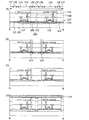
続いて、以下の工程について、図4、5を用いて説明する。図3(A)と図4(A)(B)の上面図のA−Bは、図5(A)〜(D)の断面図のA−Bに対応する。 Subsequently, the following steps will be described with reference to FIGS. A-B in the top views of FIGS. 3A and 4A and 4B corresponds to A-B in the cross-sectional views of FIGS. 5A to 5D.
基板101又は剥離層121、122に接するように、絶縁膜105を形成する(図4(A)と図5(A)参照)。絶縁膜105は、第1の領域115では剥離層121、122又は基板101に接し、第2の領域116では基板101に接する。
An insulating
続いて、絶縁膜105上に複数の素子を含む素子群106を形成する。ここでは、素子群106として、2つのトランジスタ117、118を形成する。次に、素子群106を覆うように、絶縁膜107を形成し、当該絶縁膜107上に、絶縁膜108を形成する。続いて、絶縁膜108上に、導電層110を形成する。導電層110は、アンテナとして機能する。次に、導電層110上に、保護膜として機能する絶縁膜111を形成する。上記の工程を経て、素子群106と導電層110を含む薄膜集積回路109が完成する。
Subsequently, an
なお図4(A)(B)では、トランジスタ117、118が含む半導体層の上面図を示しており、トランジスタ117、118が含むゲート電極やトランジスタ117、118上に設けられる導電層の図示は省略している。
4A and 4B are top views of semiconductor layers included in the
続いて、素子群106と導電層110が設けられた領域(以下第3の領域135とよぶ)の周囲の領域(以下第4の領域136とよぶ)に、開口部123、124を選択的に形成して、剥離層121、122を露出させる(図4(B)と図5(B)参照)。つまり、素子群106と導電層110が設けられた第3の領域135の外周に、開口部123、124を選択的に形成する。
Subsequently,
続いて、開口部123、124に剥離層121、122を除去するエッチング剤を導入して、剥離層121、122を除去する(図5(C)参照)。エッチング剤には、フッ化ハロゲンを含む気体又は液体を使用する。
Subsequently, an etching agent that removes the peeling layers 121 and 122 is introduced into the
次に、素子群106と導電層110を含む薄膜集積回路109を基体114に接着させて、薄膜集積回路109を基板101から完全に剥離する(図5(D)参照)。この際、剥離層が除去された部分は基体114に接着して、基板101と絶縁膜105が密着した部分は基板101に保持される。
Next, the thin film integrated
なお、本発明は上記の形態に制約されない。薄膜集積回路109を基体114に接着させる際、基板101と絶縁膜105が密着した部分も基体114に接着され、基板101から剥離することがある。
In addition, this invention is not restrict | limited to said form. When the thin film integrated
本作製方法では、第1の領域115の剥離層の選択的な除去の工程において、第1の領域115が含む第3の領域135と第4の領域136以外の第5の領域137の剥離層を除去し、第3の領域135と第4の領域136の剥離層を除去しないことを特徴とする。また、開口部は、第4の領域136に選択的に設けられることを特徴とする。
In this manufacturing method, the separation layer in the
つまり、第1の領域115は、第3の領域135と、第4の領域136と、第5の領域137に大別され、第3の領域135は剥離層と素子群106と導電層110が設けられた領域、第4の領域136は剥離層が設けられ、素子群106と導電層110が設けられていない領域、第5の領域137は剥離層も素子群106も導電層110も設けられていない領域に相当する。
That is, the
上記のように、剥離層を設ける箇所を選択的にすることで、剥離層を除去した後も、絶縁膜105の一部は、基板101に密着した状態にある。従って、薄膜集積回路109を基板101に保持することができ、当該薄膜集積回路109の飛散を防止することができる。
As described above, a portion of the insulating
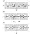
続いて、第3の作製方法について図6〜8を参照して説明する。 Subsequently, a third manufacturing method will be described with reference to FIGS.
絶縁表面を有する基板101の一表面に剥離層を形成する。次に、剥離層を選択的に除去して、剥離層が選択的に設けられた第1の領域115と、剥離層を除去した第2の領域116を形成する(図6(A)の上面図と、図6(B)の断面図参照、図6(A)の上面図のC−Dは、図6(B)の断面図のC−Dに対応する)。剥離層が選択的に設けられた第1の領域115には、後に薄膜集積回路を形成する。剥離層を除去した第2の領域116には、薄膜集積回路を形成せず、後に形成する絶縁膜と基板101とが密着した領域となる。
A separation layer is formed over one surface of the
本発明では、薄膜集積回路を1つの単位として、第1の領域115と第2の領域116が作り分けられているため、任意の薄膜集積回路のみを基体に転置することができる。また、薄膜集積回路を1つの単位として、第1の領域115と第2の領域116が作り分けられているため、基体に転置する工程を経ると、複数の薄膜集積回路の各々は自動的に分断される。そのため、複数の薄膜集積回路を分断する工程を省略することができる。
In the present invention, since the
続いて、以下の工程について、図7、図8を用いて説明する。図6(A)、図7(A)(B)の上面図のA−Bは、図8(A)〜(D)の断面図のA−Bに対応する。 Subsequently, the following steps will be described with reference to FIGS. 6A, 7A, and 7B correspond to AB in the cross-sectional views of FIGS. 8A to 8D.
基板101又は剥離層125に接するように、下地用の絶縁膜105を形成する(図7(A)と図8(A)参照)。絶縁膜105は、第1の領域115では剥離層125又は基板101に接し、第2の領域116では基板101に接する。
An insulating
続いて、絶縁膜105上に複数の素子を含む素子群106を形成する。ここでは、素子群106として、2つのトランジスタ117、118を形成する。次に、素子群106を覆うように、絶縁膜107を形成し、当該絶縁膜107上に、絶縁膜108を形成する。続いて、絶縁膜108上に、導電層110を形成する。導電層110は、アンテナとして機能する。次に、導電層110上に、保護膜として機能する絶縁膜111を形成する。上記の工程を経て、素子群106と導電層110を含む薄膜集積回路109が完成する。
Subsequently, an
なお図7(A)(B)では、トランジスタ117、118が含む半導体層の上面図を示しており、トランジスタ117、118が含むゲート電極やトランジスタ117、118上に設けられる導電層の図示は省略している。
7A and 7B are top views of semiconductor layers included in the
続いて、素子群106と導電層110が設けられた領域(以下第3の領域135とよぶ)と、第3の領域135の周囲の領域(以下第5の領域137とよぶ)以外の領域(以下第4の領域136とよぶ)に、開口部126を形成して、剥離層125を露出させる(図7(B)と図8(B)参照)。ここでは、第3の領域135は素子群106と導電層110が設けられた領域であり、第5の領域137は第3の領域135の外周の領域であり、第4の領域136は第3の領域135と第5の領域137以外の領域である。第4の領域136と第5の領域137は、第3の領域135との間の距離によって区別され、例えば、第3の領域135から、ある一定の距離の領域を第5の領域137とし、それ以外の領域を第4の領域136として区別するとよい。
Subsequently, a region other than a region where the
続いて、開口部126に、剥離層125を除去するエッチング剤を導入して、剥離層125を除去する(図8(C)参照)。エッチング剤には、フッ化ハロゲンを含む気体又は液体を使用する。
Subsequently, an etching agent for removing the
次に、素子群106と導電層110を含む薄膜集積回路109を基体114に接着させて、薄膜集積回路109を基板101から完全に剥離する(図8(D)参照)。この際、剥離層が除去された部分は基体114に接着して、基板101と絶縁膜105が密着した部分は基板101に保持される。
Next, the thin film integrated
なお、本発明は上記の形態に制約されない。薄膜集積回路109を基体114に接着させる際、基板101と絶縁膜105が密着した部分も基体114に接着され、基板101から剥離することがある。
In addition, this invention is not restrict | limited to said form. When the thin film integrated
本作製方法では、第1の領域115の剥離層の選択的な除去の工程において、第1の領域115が含む第5の領域137の剥離層を選択的に除去し、第3の領域135と第4の領域136の剥離層を除去しないことを特徴とする。
In this manufacturing method, in the step of selectively removing the separation layer in the
つまり、第1の領域115は、第3の領域135と、第4の領域136と、第5の領域137に大別され、第3の領域135は剥離層と素子群106と導電層110が設けられた領域、第5の領域137は剥離層が選択的に設けられ、素子群106と導電層110が設けられていない領域、第4の領域136は剥離層が設けられ、素子群106と導電層110が設けられていない領域に相当する。また、第4の領域136は、開口部が設けられる領域に相当する。
That is, the
上記のように、剥離層を設ける箇所を選択的にすることで、剥離層を除去した後も、絶縁膜105の一部は、基板101に密着した状態にある。従って、薄膜集積回路109を基板101に保持することが可能となり、当該薄膜集積回路109の飛散を防止することができる。
As described above, a portion of the insulating
次に、第4の作製方法について、図9、10を参照して説明する。 Next, a fourth manufacturing method will be described with reference to FIGS.
絶縁表面を有する基板101の一表面に剥離層を形成する。次に、剥離層を選択的に除去して、剥離層が選択的に設けられた第1の領域115と、剥離層を除去した第2の領域116を形成する(図6(A)の上面図と、図6(B)の断面図参照)。この工程は、上記の第3の方法と同じである。
A separation layer is formed over one surface of the
続いて、以下の工程について、図9、10を用いて説明する。図9の上面図のA−Bは、図10の断面図のA−Bに対応する。 Next, the following steps will be described with reference to FIGS. 9 corresponds to AB in the cross-sectional view in FIG. 10.
基板101又は剥離層131に接するように、下地用の絶縁膜105を形成する(図9(B)と図10(A)参照)。絶縁膜105は、第1の領域115では剥離層131又は基板101に接し、第2の領域116では基板101に接する。図9(A)において、剥離層131が設けられていない領域は、斜線が引かれていない四角で示す領域である。
An insulating
続いて、絶縁膜105上に複数の素子を含む素子群106を形成する。ここでは、素子群106として、2つのトランジスタ117、118を形成する。次に、素子群106を覆うように、絶縁膜107を形成し、当該絶縁膜107上に、絶縁膜108を形成する。続いて、絶縁膜108上に、導電層110を形成する。導電層110は、アンテナとして機能する。次に、導電層110上に、保護膜として機能する絶縁膜111を形成する。上記の工程を経て、素子群106と導電層110を含む薄膜集積回路109が完成する。
Subsequently, an
なお図9(A)〜(C)では、トランジスタ117、118が含む半導体層の上面図を示しており、トランジスタ117、118が含むゲート電極やトランジスタ117、118上に設けられる導電層の図示は省略している。
9A to 9C are top views of the semiconductor layers included in the
なお、本工程では、基板101と絶縁膜105が密着する領域は、薄膜集積回路109が設けられた領域と重なるように設けられる。このような基板101と絶縁膜105が密着する領域は、薄膜集積回路109を基体114に接着させる際に、基板101から剥離される。従って、基板101と絶縁膜105が密着する領域は、できる限り小さく設けるとよい。
Note that in this step, the region where the
続いて、素子群106と導電層110が設けられた領域(以下第3の領域135とよぶ)以外の領域(以下第4の領域136とよぶ)に、開口部132を選択的に形成して、剥離層131を露出させる(図9(C)と図10(B)参照)。
Subsequently, an
続いて、開口部132に剥離層131を除去するエッチング剤を導入して、剥離層131を除去する(図10(C)参照)。エッチング剤には、フッ化ハロゲンを含む気体又は液体を使用する。
Subsequently, an etchant that removes the
次に、素子群106と導電層110を含む薄膜集積回路109を基体114に接着させて、薄膜集積回路109を基板101から完全に剥離する(図10(D)参照)。この際、剥離層が除去された部分だけでなく、基板101と絶縁膜105が密着していた部分も基体114に接着される。
Next, the thin film integrated
なお、本発明は上記の形態に制約されない。薄膜集積回路109を基体114に接着させる際、基板101と絶縁膜105が密着した部分も基体114に接着され、基板101から剥離することがある。
In addition, this invention is not restrict | limited to said form. When the thin film integrated
本作製方法では、第1の領域115の剥離層の選択的な除去の工程では、第1の領域115が含む第3の領域135の剥離層を選択的に除去し、第4の領域136の剥離層を除去しないことを特徴とする。
In this manufacturing method, in the step of selectively removing the separation layer in the
つまり、第1の領域115は、第3の領域135と、第4の領域136に大別され、第3の領域135は選択的に設けられた剥離層と素子群106と導電層110が設けられた領域、第4の領域136は剥離層が設けられ、素子群106と導電層110が設けられていない領域に相当する。また、第4の領域136は、開口部が設けられる領域に相当する。
That is, the
上記のように、剥離層を設ける箇所を選択的にすることで、剥離層を除去した後も、絶縁膜105の一部は、基板101に密着した状態にある。従って、薄膜集積回路109を基板101に保持することが可能となり、当該薄膜集積回路109の飛散を防止することができる。
As described above, a portion of the insulating
なお、上記の第1乃至第4の作製方法において、第2の領域116の剥離層は全て除去していたが、本発明はこの工程に限定されない。第2の領域116の剥離層を選択的に除去してもよい。例えば、第1の作製方法の場合、第1の領域115の剥離層を除去せず、第2の領域116の剥離層は選択的に除去してもよい(図11(A)参照)。また、第2の作製方法の場合、第1の領域115と第4の領域116の剥離層を共に選択的に除去してもよい(図11(B)参照)。また、第3の作製方法と第4の作製方法の場合も、第1の領域115と第2の領域116の剥離層を共に選択的に除去してもよい(図11(C)参照)。
Note that in the first to fourth manufacturing methods, the peeling layer in the
図11(A)〜(C)の上面図において、第1の領域115は、四角形状で、かつ点線で囲まれた領域である。第2の領域116は、第1の領域115以外の領域である。第1の領域115は、第2の領域116に囲まれている。
In the top views of FIGS. 11A to 11C, the
上記のように、第2の領域116の剥離層を選択的に除去することで、薄膜集積回路109の基板101に対する保持をより確実に行うことが可能となり、当該薄膜集積回路109の飛散を防止することができる。
As described above, by selectively removing the peeling layer in the
上記の工程を経て剥離された薄膜集積回路109は、そのまま用いてもよいし、基体により封止した後に用いてもよい。本発明は絶縁基板上に形成された薄膜集積回路109を用いるため、円形のシリコン基板から形成されたチップと比較して、母体基板の形状に制約がない。そのため、生産性を高め、大量生産を可能とし、低コスト化を実現する。また、本発明は、0.2μm以下、代表的には40nm〜170nm、好ましくは50nm〜150nmの膜厚の半導体膜を能動領域として用いることができるため、非常に薄型となり、物品に実装しても、薄膜集積回路の存在が認識しづらく、改ざん防止につながる。
The thin film integrated
本発明により作製される薄膜集積回路は、複数の素子と、アンテナとして機能する導電層とを有する。複数の素子とは、例えば、薄膜トランジスタ、容量素子、抵抗素子、ダイオード等に相当する。 A thin film integrated circuit manufactured according to the present invention includes a plurality of elements and a conductive layer functioning as an antenna. The plurality of elements correspond to, for example, a thin film transistor, a capacitor element, a resistance element, a diode, and the like.
薄膜集積回路210は、非接触でデータを交信する機能を有し、当該薄膜集積回路210が含む複数の素子は様々な回路を構成する。例えば、電源回路211、クロック発生回路212、データ復調/変調回路213、制御回路214、インターフェイス回路215、メモリ216、データバス217、アンテナ(アンテナコイルともよぶ)218等を有する(図12参照)。
The thin film integrated
電源回路211は、アンテナ218から入力された交流信号を基に、上記の各回路に供給する各種電源を生成する回路である。クロック発生回路212は、アンテナ218から入力された交流信号を基に、上記の各回路に供給する各種クロックを生成する回路である。データ復調/変調回路213は、リーダライタ219と交信するデータを復調又は変調する機能を有する。制御回路214は、例えば、中央処理ユニット(CPU、Central Processing Unit)やマイクロプロセッサ(MPU、MicroProcessor Unit)等に相当し、他の回路を制御する機能を有する。アンテナ218は、電磁界或いは電波の送受信を行う機能を有する。リーダライタ219は、薄膜集積回路との交信、制御及びそのデータに関する処理を制御する。
The
なお、薄膜集積回路が構成する回路は上記構成に制約されず、例えば、電源電圧のリミッタ回路や暗号処理専用ハードウエアといった他の構成要素を追加した構成であってもよい。 Note that the circuit included in the thin film integrated circuit is not limited to the above-described configuration, and may be a configuration in which other components such as a power supply voltage limiter circuit and cryptographic processing dedicated hardware are added.
本発明により作製される薄膜集積回路の用途は広範にわたるが、例えば、紙幣、硬貨、有価証券類、無記名債券類、証書類(運転免許証や住民票等、図13(A)参照)、包装用容器類(包装紙やボトル等、図13(B)参照)、記録媒体(DVDソフトやビデオテープ等、図13(C)参照)、乗物類(自転車等、図13(D)参照)、身の回り品(鞄や眼鏡等、図13(E)参照)、食品類、衣類、生活用品類、電子機器等に設けて使用することができる。電子機器とは、液晶表示装置、EL表示装置、テレビジョン装置(単にテレビ、テレビ受像機、テレビジョン受像機とも呼ぶ)及び携帯電話等を指す。 The thin film integrated circuit manufactured according to the present invention has a wide range of applications. For example, banknotes, coins, securities, bearer bonds, certificates (driver's license, resident's card, etc., see FIG. 13A), packaging Containers (wrapping paper, bottles, etc., see FIG. 13B), recording media (DVD software, video tape, etc., see FIG. 13C), vehicles (bicycles, see FIG. 13D), It can be used in personal items (such as bags and glasses, see FIG. 13E), foods, clothing, daily necessities, electronic devices, and the like. Electronic devices refer to liquid crystal display devices, EL display devices, television devices (also simply referred to as televisions, television receivers, television receivers), mobile phones, and the like.
なお、薄膜集積回路は、物品の表面に貼ったり、物品に埋め込んだりして、物品に固定される。例えば、物品が本なら紙に薄膜集積回路を埋め込んだり、物品が有機樹脂からなるパッケージなら有機樹脂に薄膜集積回路を埋め込んだりするとよい。紙幣、硬貨、有価証券類、無記名債券類、証書類等に薄膜集積回路を設けることにより、偽造を防止することができる。また、包装用容器類、記録媒体、身の回り品、食品類、衣類、生活用品類、電子機器等に薄膜集積回路を設けることにより、検品システムやレンタル店のシステムなどの効率化を図ることができる。乗物類に薄膜集積回路を設けることにより、偽造や盗難を防止することができる。 Note that the thin film integrated circuit is fixed to the article by being attached to the surface of the article or embedded in the article. For example, if the article is a book, the thin film integrated circuit may be embedded in paper, and if the article is a package made of an organic resin, the thin film integrated circuit may be embedded in the organic resin. Forgery can be prevented by providing a thin film integrated circuit for bills, coins, securities, bearer bonds, certificates, etc. In addition, by providing thin film integrated circuits in packaging containers, recording media, personal items, foods, clothing, daily necessities, electronic devices, etc., the efficiency of inspection systems and rental store systems can be improved. . Forgery and theft can be prevented by providing a thin film integrated circuit in a vehicle.
また、薄膜集積回路を、物の管理や流通のシステムに応用することで、システムの高機能化を図ることができる。例えば、表示部294を含む携帯端末の側面にリーダライタ295を設けて、物品297の側面に薄膜集積回路296を設ける場合が挙げられる(図14(A)参照)。この場合、リーダライタ295に薄膜集積回路296をかざすと、表示部294に物品297の原材料や原産地、流通過程の履歴等の情報が表示されるシステムになっている。また、別の例として、ベルトコンベアの脇にリーダライタ295を設ける場合が挙げられる(図14(B)参照)。この場合、物品297の検品を簡単に行うことができる。このように、薄膜集積回路を、システムに応用することで、システムの多機能化を図ることができる。
Further, by applying the thin film integrated circuit to a system for managing and distributing objects, it is possible to improve the function of the system. For example, there is a case where a reader /
上記の実施の形態では、剥離層は、珪素を含む層をスパッタリング法やプラズマCVD法等の公知の方法により形成するとあるが、本発明は、珪素を含む層に限定されない。剥離層は、例えば、公知の手段(スパッタリング法やプラズマCVD法等)により、タングステン(W)、モリブデン(Mo)、チタン(Ti)、タンタル(Ta)、ニオブ(Nb)、ニッケル(Ni)、コバルト(Co)、ジルコニウム(Zr)、亜鉛(Zn)、ルテニウム(Ru)、ロジウム(Rh)、パラジウム(Pd)、オスミウム(Os)、イリジウム(Ir)、珪素(Si)から選択された元素または前記元素を主成分とする合金材料若しくは化合物材料からなる層を、単層又は積層して形成してもよい。 In the above embodiment, the release layer is formed by forming a layer containing silicon by a known method such as a sputtering method or a plasma CVD method; however, the present invention is not limited to the layer containing silicon. The release layer is formed by, for example, a known means (sputtering method, plasma CVD method, etc.) tungsten (W), molybdenum (Mo), titanium (Ti), tantalum (Ta), niobium (Nb), nickel (Ni), An element selected from cobalt (Co), zirconium (Zr), zinc (Zn), ruthenium (Ru), rhodium (Rh), palladium (Pd), osmium (Os), iridium (Ir), silicon (Si) or A layer made of an alloy material or a compound material containing the element as a main component may be formed as a single layer or a stacked layer.
剥離層が単層構造の場合、好ましくは、タングステンを含む層、モリブデンを含む層、タングステンとモリブデンの混合物を含む層、タングステンの酸化物を含む層、タングステンの酸化窒化物を含む層、モリブデンの酸化物を含む層、モリブデンの酸化窒化物を含む層、タングステンとモリブデンの混合物の酸化物、タングステンとモリブデンの混合物の酸化窒化物を含む層を形成する。なお、タングステンとモリブデンの混合物とは、例えば、タングステンとモリブデンの合金に相当する。 In the case where the separation layer has a single-layer structure, preferably, a layer containing tungsten, a layer containing molybdenum, a layer containing a mixture of tungsten and molybdenum, a layer containing tungsten oxide, a layer containing tungsten oxynitride, A layer containing an oxide, a layer containing molybdenum oxynitride, an oxide of a mixture of tungsten and molybdenum, and a layer containing an oxynitride of a mixture of tungsten and molybdenum are formed. Note that the mixture of tungsten and molybdenum corresponds to, for example, an alloy of tungsten and molybdenum.
剥離層が積層構造の場合、好ましくは、1層目としてタングステンを含む層、モリブデンを含む層、又はタングステンとモリブデンの混合物を含む層を形成し、2層目として、タングステンを含む層、モリブデンを含む層、タングステンとモリブデンの混合物の酸化物を含む層、タングステンとモリブデンの混合物の窒化物を含む層、タングステンとモリブデンの混合物の酸化窒化物を含む層、タングステンとモリブデンの混合物の窒化酸化物を含む層を形成する。 In the case where the separation layer has a stacked structure, preferably, a layer containing tungsten, a layer containing molybdenum, or a layer containing a mixture of tungsten and molybdenum is formed as a first layer, and a layer containing tungsten or molybdenum is formed as a second layer. A layer containing an oxide of a mixture of tungsten and molybdenum, a layer containing a nitride of a mixture of tungsten and molybdenum, a layer containing an oxynitride of a mixture of tungsten and molybdenum, a nitride oxide of a mixture of tungsten and molybdenum Forming a containing layer;
なお、剥離層として、タングステンを含む層、タングステンの酸化物を含む層の2層の積層構造を形成する場合、タングステンを含む層を形成し、その上層に酸化珪素を含む層を形成することで、タングステン層と酸化珪素層との界面に、タングステンの酸化物を含む層が形成されることを活用してもよい。これは、他の積層構造を形成する場合も同様であり、例えば、タングステンを含む層、タングステンの窒化物、酸化窒化物又は窒化酸化物を含む層の2層の積層構造を形成する場合、タングステンを含む層を形成後、その上層に窒化珪素層、酸素を含む窒化珪素層、窒素を含む酸化珪素層を形成する。 Note that in the case where a two-layer structure including a layer containing tungsten and a layer containing tungsten oxide is formed as the separation layer, a layer containing tungsten is formed, and a layer containing silicon oxide is formed thereon. The formation of a layer containing an oxide of tungsten at the interface between the tungsten layer and the silicon oxide layer may be utilized. The same applies to the case of forming another stacked structure. For example, when forming a stacked structure of two layers of a layer containing tungsten, a nitride of tungsten, a layer containing oxynitride, or a nitrided oxide, tungsten is formed. After forming the layer containing silicon, a silicon nitride layer, a silicon nitride layer containing oxygen, and a silicon oxide layer containing nitrogen are formed thereon.
また、エッチング剤として、ハロゲン化物を含む気体又は液体を用いてもよい。ハロゲン化物として、例えば、三フッ化塩素(ClF3)、三フッ化窒素(NF3)、三フッ化臭素(BrF3)、フッ化水素(HF)を用いてもよい。なお、フッ化水素(HF)を用いる場合 は、剥離層として、珪素の酸化物を用いる。本実施例は、他の実施の形態、実施例と自由に組み合わせることができる。 Further, a gas or a liquid containing a halide may be used as an etching agent. As the halide, for example, chlorine trifluoride (ClF 3 ), nitrogen trifluoride (NF 3 ), bromine trifluoride (BrF 3 ), or hydrogen fluoride (HF) may be used. Note that in the case of using hydrogen fluoride (HF), a silicon oxide is used for the separation layer. This embodiment can be freely combined with other embodiment modes and embodiments.
上記の実施の形態では、薄膜集積回路109を基体114に接着させることにより、薄膜集積回路109を基板101から剥離するまでの工程について述べた。本実施例では、その後の工程について、図15を参照して説明する。
In the above embodiment, the process until the thin film integrated
薄膜集積回路109の一方の面を基体114に接着させた後は、薄膜集積回路109の他方の面を基体140に接着させる。その後、基体114と基体140が互いに接着した部分を、切断手段141で切断する。そうすると、封止された1つの薄膜集積回路109が完成する。切断手段141は、ダイシング装置、スクライビング装置、レーザー照射装置(特にCO2レーザー照射装置)、ナイフ等に相当する。そして、封止された薄膜集積回路109は、出荷される。
After one surface of the thin film integrated
基体114と基体140(基板、フィルム、テープとよぶこともできる)は、フィルムや繊維質な材料からなる紙などに相当する。フィルムは、ポリプロピレン、ポリエステル、ビニル、ポリフッ化ビニル、塩化ビニル、エチレンビニルアセテート等の材料からなる。なお、基体114と基体140の表面は、二酸化珪素(シリカ)の粉末により、コーティングされていてもよい。このコーティングにより、高温で高湿度の環境下においても防水性を保つことができる。また、基体114と基体140の表面を、インジウム錫酸化物等の導電性材料によりコーティングされていてもよい。コーティングにより、静電気がチャージされ、薄膜集積回路109を保護することができる。また、基体114と基体140の一方又は両方は、保護膜として、炭素を主成分とする薄膜(ダイヤモンドライクカーボン膜)によりコーティングされていてもよい。
The
また、基体114と基体140の一方又は両方は、一方の面に接着面を有していてもよい。接着面は、熱硬化樹脂、紫外線硬化樹脂、エポキシ樹脂系接着剤等の接着剤を塗布したものである。また、基体114と基体140の一方又は両方は、透光性を有していてもよい。本実施例は、他の実施の形態、実施例と自由に組み合わせることができる。
One or both of the
上述の実施の形態では、基板上に、剥離層、絶縁膜の順に積層して形成する方法について説明した。例えば、第1の作製方法では、基板101又は剥離層102〜104に接するように、絶縁膜105を形成している(図2(A)参照)。第2の作製方法では、基板101又は剥離層121、122に接するように、絶縁膜105を形成している(図5(A)参照)。第3の作製方法では、基板101又は剥離層125に接するように、絶縁膜105を形成している(図8(A)参照)。第4の作製方法では、基板101又は剥離層131に接するように、絶縁膜105を形成している(図10(A)参照)。しかしながら、本発明はこれに制約されない。基板上に、第1の絶縁膜、剥離層、第2の絶縁膜の順に積層して形成してもよい。
In the above-described embodiment, the method of stacking the peeling layer and the insulating film in this order on the substrate has been described. For example, in the first manufacturing method, the insulating
つまり、基板の一表面に第1の絶縁膜を形成し、第1の絶縁膜上に剥離層を形成する。次に、剥離層を選択的に除去して、剥離層が設けられた第1の領域と、剥離層が設けられていない第2の領域を形成する。続いて、第2の絶縁膜を全面に形成する。具体的には、第1の領域では剥離層に接し、第2の領域では第1の絶縁膜に接するように、第2の絶縁膜を形成する。そうすると、第1の領域では、基板上に、第1の絶縁膜、剥離層、第2の絶縁膜が順に積層して設けられ、第2の領域では、第1の絶縁膜、第2の絶縁膜が順に積層して設けられる。 That is, a first insulating film is formed on one surface of the substrate, and a peeling layer is formed on the first insulating film. Next, the release layer is selectively removed to form a first region where the release layer is provided and a second region where the release layer is not provided. Subsequently, a second insulating film is formed on the entire surface. Specifically, the second insulating film is formed so as to be in contact with the separation layer in the first region and in contact with the first insulating film in the second region. Then, in the first region, the first insulating film, the release layer, and the second insulating film are sequentially stacked on the substrate, and in the second region, the first insulating film and the second insulating film are provided. Films are sequentially stacked.
次に、第1の領域の第2の絶縁膜上に複数の素子とアンテナとして機能する導電層を含む薄膜集積回路を形成し、続いて開口部を形成し、その後、開口部にエッチング剤を導入して剥離層を除去する。そうすると、第1の領域では、第1の絶縁膜と第2の絶縁膜の間に空間が生じるが、第2の領域では、基板、第1の絶縁膜、第2の絶縁膜が順に密着して積層されたままとなる。 Next, a thin film integrated circuit including a plurality of elements and a conductive layer functioning as an antenna is formed over the second insulating film in the first region, and then an opening is formed. After that, an etching agent is formed in the opening. Introduce and remove the release layer. Then, in the first region, a space is generated between the first insulating film and the second insulating film, but in the second region, the substrate, the first insulating film, and the second insulating film are in close contact with each other in order. And remain stacked.
このように、剥離層を除去した後も、基板上に、第1の絶縁膜と第2の絶縁膜が密着した領域が設けられていることにより、第2の絶縁膜の上方に設けられた薄膜集積回路の飛散を防止することができる。また、基板上に、第1の絶縁膜と第2の絶縁膜が密着した領域が設けられていることで、基板上に薄膜集積回路を保持することができ、当該薄膜集積回路の基体への転置を容易に行うことができる。 As described above, even after the release layer is removed, the region where the first insulating film and the second insulating film are in close contact with each other is provided on the substrate, so that the first insulating film is provided above the second insulating film. Scattering of the thin film integrated circuit can be prevented. In addition, since the region where the first insulating film and the second insulating film are in close contact with each other is provided on the substrate, the thin film integrated circuit can be held on the substrate, and the substrate of the thin film integrated circuit can be connected to the base. Transposition can be performed easily.
また、第1の絶縁膜を設けることにより、ガラス基板からの不純物の侵入を防止することができる。また、剥離層を選択的に形成する際、剥離層をパターン加工するが、その際、剥離層だけでなく、基板がエッチングされてしまうことがある。しかしながら、第1の絶縁膜を形成することにより、基板がエッチングされてしまうことを防止することができる。第1の絶縁膜は、プラズマCVD法やスパッタリング法等の公知の方法を用いて、珪素の酸化物、珪素の窒化物、窒素が添加された珪素の酸化物、酸素が添加された珪素の窒化物等からなる薄膜を形成する。 In addition, by providing the first insulating film, impurities can be prevented from entering from the glass substrate. Further, when the release layer is selectively formed, the release layer is subjected to pattern processing. At that time, not only the release layer but also the substrate may be etched. However, by forming the first insulating film, the substrate can be prevented from being etched. The first insulating film is formed using a known method such as a plasma CVD method or a sputtering method using silicon oxide, silicon nitride, silicon oxide added with nitrogen, or silicon nitride added with oxygen. A thin film made of material is formed.
以下には、基板上に、第1の絶縁膜、剥離層、第2の絶縁膜の順に作製する作製方法について説明する。 Hereinafter, a manufacturing method in which a first insulating film, a separation layer, and a second insulating film are formed in this order over a substrate will be described.
第1の作製方法では、まず、基板101上に絶縁膜119(第1の絶縁膜に相当)を形成する(図16(A)参照)。次に、絶縁膜119上に、選択的に剥離層102〜104を形成する。続いて、絶縁膜119又は剥離層102〜104に接するように、絶縁膜105(第2の絶縁膜に相当)を形成する。そうすると、絶縁膜105は、第1の領域115では剥離層102〜104に接し、第2の領域116では絶縁膜119に接する。その後は、上述した通り、第1の領域115の絶縁膜105上に、複数の素子106とアンテナとして機能する導電層110を形成する。次に、第1の領域115に、剥離層102〜104が露出される開口部を選択的に形成する。次に、開口部にエッチング剤を導入して、剥離層102〜104を除去する。
In the first manufacturing method, first, an insulating film 119 (corresponding to the first insulating film) is formed over the substrate 101 (see FIG. 16A). Next, separation layers 102 to 104 are selectively formed over the insulating
第2の作製方法では、まず、基板101上に絶縁膜119(第1の絶縁膜に相当)を形成する(図16(B)参照)。次に、絶縁膜119上に、選択的に剥離層121、122を形成する。続いて、絶縁膜119又は剥離層121、122に接するように、絶縁膜105(第2の絶縁膜に相当)を形成する。そうすると、絶縁膜105は、第1の領域115では、剥離層121、122又は絶縁膜119に接し、第2の領域116では、絶縁膜119に接する。その後は、上述した通り、第1の領域115の絶縁膜105上に、複数の素子106とアンテナとして機能する導電層110を形成する。次に、第1の領域115に、剥離層121、122が露出される開口部を選択的に形成する。次に、開口部にエッチング剤を導入して、剥離層121、122を除去する。
In the second manufacturing method, first, an insulating film 119 (corresponding to the first insulating film) is formed over the substrate 101 (see FIG. 16B). Next, separation layers 121 and 122 are selectively formed over the insulating
第3の作製方法では、まず、基板101上に絶縁膜119(第1の絶縁膜に相当)を形成する(図17(A)参照)。次に、絶縁膜119上に、選択的に剥離層125を形成する。続いて、絶縁膜119又は剥離層125に接するように、絶縁膜105(第2の絶縁膜に相当)を形成する。そうすると、絶縁膜105は、第1の領域115では、剥離層125又は絶縁膜119に接し、第2の領域116では、絶縁膜119に接する。その後は、上述した通り、第1の領域115の絶縁膜105上に、複数の素子106とアンテナとして機能する導電層110を形成する。次に、第1の領域115に、剥離層125が露出される開口部を選択的に形成する。次に、開口部にエッチング剤を導入して、剥離層125を除去する。
In the third manufacturing method, first, an insulating film 119 (corresponding to the first insulating film) is formed over the substrate 101 (see FIG. 17A). Next, a
第4の作製方法では、まず、基板101上に絶縁膜119(第1の絶縁膜に相当)を形成する(図17(B)参照)。次に、絶縁膜119上に、選択的に剥離層131を形成する。続いて、絶縁膜119又は剥離層131に接するように、絶縁膜105(第2の絶縁膜に相当)を形成する。そうすると、絶縁膜105は、第1の領域115では、剥離層131又は絶縁膜119に接し、第2の領域116では、絶縁膜119に接する。その後は、上述した通り、第1の領域115の絶縁膜105上に、複数の素子106とアンテナとして機能する導電層110を形成する。次に、第1の領域115に、剥離層121が露出される開口部を選択的に形成する。次に、開口部にエッチング剤を導入して、剥離層121を除去する。
In the fourth manufacturing method, first, an insulating film 119 (corresponding to the first insulating film) is formed over the substrate 101 (see FIG. 17B). Next, a
なお、上記の作製方法では、薄膜集積回路として、複数の素子と、アンテナとして機能する導電層を形成しているが、本発明はこの構成に制約されない。電磁波を送受信する機能を有する半導体装置を形成する場合、複数の素子のみ、又は複数の素子とアンテナとして機能する導電層を形成するとよい。 Note that in the above manufacturing method, a plurality of elements and a conductive layer functioning as an antenna are formed as a thin film integrated circuit; however, the present invention is not limited to this structure. In the case of forming a semiconductor device having a function of transmitting and receiving electromagnetic waves, a plurality of elements or a conductive layer that functions as an antenna and an antenna may be formed.
101 基板
102 剥離層
103 剥離層
104 剥離層
105 絶縁膜
106 素子群
107 絶縁膜
108 絶縁膜
109 薄膜集積回路
110 導電層
111 絶縁膜
112 開口部
113 開口部
114 基体
115 第1の領域
116 第2の領域
117 トランジスタ
118 トランジスタ
119 絶縁膜
121 剥離層
122 剥離層
123 開口部
124 開口部
125 剥離層
126 開口部
131 剥離層
132 開口部
135 第3の領域
136 第4の領域
137 第5の領域
140 基体
101
Claims (9)
前記第2の領域の前記剥離層を除去し、
前記第1の領域の前記剥離層上と前記第2の領域の前記基板上に、絶縁膜を形成し、
前記第1の領域の前記絶縁膜上に、複数の素子と導電層を形成し、
前記第1の領域の前記絶縁膜に、前記剥離層が露出される開口部を形成し、
前記第1の領域の前記開口部にエッチング剤を導入して、前記剥離層を除去することを特徴とする薄膜集積回路の作製方法。 Forming a release layer on the first region and the second region over the substrate having an insulating surface;
Removing the release layer in the second region;
Forming an insulating film on the release layer in the first region and on the substrate in the second region;
Forming a plurality of elements and a conductive layer on the insulating film in the first region;
Forming an opening through which the release layer is exposed in the insulating film of the first region;
A method for manufacturing a thin film integrated circuit, wherein an etchant is introduced into the opening in the first region to remove the release layer.
前記第1の領域の前記剥離層を選択的に除去し、
前記第2の領域の前記剥離層を除去し、
前記第1の領域の前記基板及び前記剥離層上と前記第2の領域の前記基板上に、絶縁膜を形成し、
前記第1の領域の前記絶縁膜上に、複数の素子と導電層を形成し、
前記第1の領域の前記絶縁膜に、前記剥離層が露出される開口部を形成し、
前記第1の領域の前記開口部にエッチング剤を導入して、前記剥離層を除去し、
前記第1の領域の前記剥離層を選択的に除去する工程では、前記第1の領域に含まれ前記複数の素子と前記導電層が設けられた第3の領域の前記剥離層は除去せず、前記第1の領域に含まれ前記開口部が設けられた第4の領域の前記剥離層は除去せず、前記第1の領域に含まれ前記第3の領域と前記第4の領域を除く第5の領域の前記剥離層を除去することを特徴とする薄膜集積回路の作製方法。 Forming a release layer on the first region and the second region over the substrate having an insulating surface;
Selectively removing the release layer in the first region;
Removing the release layer in the second region;
On the substrate of the first region and the substrate and the second region and the release layer on the, to form an insulating film,
Forming a plurality of elements and a conductive layer on the insulating film in the first region;
Forming an opening through which the release layer is exposed in the insulating film of the first region;
Introducing an etchant into the opening in the first region to remove the release layer;
In the step of selectively removing the release layer in the first region, the release layer in the third region included in the first region and provided with the plurality of elements and the conductive layer is not removed. The release layer in the fourth region included in the first region and provided with the opening is not removed, and the third region and the fourth region are included in the first region. A method for manufacturing a thin film integrated circuit, wherein the release layer in the fifth region is removed.
前記第1の領域の前記剥離層を選択的に除去し、
前記第2の領域の前記剥離層を除去し、
前記第1の領域の前記基板及び前記剥離層上と前記第2の領域の前記基板上に、絶縁膜を形成し、
前記第1の領域の前記絶縁膜上に、複数の素子と導電層を形成し、
前記第1の領域の前記絶縁膜に、前記剥離層が露出される開口部を形成し、
前記第1の領域の前記開口部にエッチング剤を導入して、前記剥離層を除去し、
前記第1の領域の前記剥離層を選択的に除去する工程では、前記第1の領域に含まれ前記複数の素子と前記導電層が設けられた第3の領域の前記剥離層は除去せず、前記第1の領域に含まれ前記開口部が設けられた第4の領域の前記剥離層は除去せず、前記第1の領域に含まれ前記第3の領域と前記第4の領域を除く第5の領域の前記剥離層を選択的に除去することを特徴とする薄膜集積回路の作製方法。 Forming a release layer on the first region and the second region over the substrate having an insulating surface;
Selectively removing the release layer in the first region;
Removing the release layer in the second region;
On the substrate of the first region and the substrate and the second region and the release layer on the, to form an insulating film,
Forming a plurality of elements and a conductive layer on the insulating film in the first region;
Forming an opening through which the release layer is exposed in the insulating film of the first region;
Introducing an etchant into the opening in the first region to remove the release layer;
In the step of selectively removing the release layer in the first region, the release layer in the third region included in the first region and provided with the plurality of elements and the conductive layer is not removed. The release layer in the fourth region included in the first region and provided with the opening is not removed, and the third region and the fourth region are included in the first region. A method for manufacturing a thin film integrated circuit, wherein the peeling layer in a fifth region is selectively removed.
前記第1の領域の前記剥離層を選択的に除去し、
前記第2の領域の前記剥離層を除去し、
前記第1の領域の前記基板及び前記剥離層上と前記第2の領域の前記基板上に、絶縁膜を形成し、
前記第1の領域の前記絶縁膜上に、複数の素子と導電層を形成し、
前記第1の領域の前記絶縁膜に、前記剥離層が露出される開口部を形成し、
前記第1の領域の前記開口部にエッチング剤を導入して、前記剥離層を除去し、
前記第1の領域の前記剥離層を選択的に除去する工程では、前記第1の領域に含まれ前記複数の素子と前記導電層が設けられた第3の領域の前記剥離層を選択的に除去し、前記第1の領域に含まれ前記開口部が設けられた第4の領域の前記剥離層を除去しないことを特徴とする薄膜集積回路の作製方法。 Forming a release layer on the first region and the second region over the substrate having an insulating surface;
Selectively removing the release layer in the first region;
Removing the release layer in the second region;
On the substrate of the first region and the substrate and the second region and the release layer on the, to form an insulating film,
Forming a plurality of elements and a conductive layer on the insulating film in the first region;
Forming an opening through which the release layer is exposed in the insulating film of the first region;
Introducing an etchant into the opening in the first region to remove the release layer;
In the step of selectively removing the release layer in the first region, the release layer in the third region included in the first region and provided with the plurality of elements and the conductive layer is selectively selected. A method for manufacturing a thin film integrated circuit, wherein the peeling layer is not removed and the peeling layer in the fourth region included in the first region and provided with the opening is not removed.
前記第2の領域の前記剥離層を選択的に除去することを特徴とする薄膜集積回路の作製方法。 In any one of Claims 1 thru | or 4,
A method for manufacturing a thin film integrated circuit, wherein the peeling layer in the second region is selectively removed.
前記絶縁膜は、前記第1の領域の前記剥離層と前記第2の領域の前記基板に接するように、形成されることを特徴とする薄膜集積回路の作製方法。 In claim 1,
The method for manufacturing a thin film integrated circuit, wherein the insulating film is formed so as to be in contact with the peeling layer in the first region and the substrate in the second region.
前記絶縁膜は、前記第1の領域の前記基板及び前記剥離層と、前記第2の領域の前記基板に接するように、形成されることを特徴とする薄膜集積回路の作製方法。 In any one of Claims 2 thru | or 4,
The method for manufacturing a thin film integrated circuit, wherein the insulating film is formed so as to be in contact with the substrate and the release layer in the first region and the substrate in the second region.
前記エッチング剤は、フッ化ハロゲンを含む気体又は液体であることを特徴とする薄膜集積回路の作製方法。 In any one of Claims 1 thru | or 7,
The method for manufacturing a thin film integrated circuit, wherein the etching agent is a gas or a liquid containing halogen fluoride.
前記導電層は、アンテナとして機能することを特徴とする薄膜集積回路の作製方法。 In any one of Claims 1 thru | or 8,
The method for manufacturing a thin film integrated circuit, wherein the conductive layer functions as an antenna.
Priority Applications (1)
| Application Number | Priority Date | Filing Date | Title |
|---|---|---|---|
| JP2005185380A JP4912627B2 (en) | 2004-06-24 | 2005-06-24 | Method for manufacturing thin film integrated circuit |
Applications Claiming Priority (3)
| Application Number | Priority Date | Filing Date | Title |
|---|---|---|---|
| JP2004186543 | 2004-06-24 | ||
| JP2004186543 | 2004-06-24 | ||
| JP2005185380A JP4912627B2 (en) | 2004-06-24 | 2005-06-24 | Method for manufacturing thin film integrated circuit |
Publications (3)
| Publication Number | Publication Date |
|---|---|
| JP2006041502A JP2006041502A (en) | 2006-02-09 |
| JP2006041502A5 JP2006041502A5 (en) | 2008-05-15 |
| JP4912627B2 true JP4912627B2 (en) | 2012-04-11 |
Family
ID=35906104
Family Applications (1)
| Application Number | Title | Priority Date | Filing Date |
|---|---|---|---|
| JP2005185380A Expired - Fee Related JP4912627B2 (en) | 2004-06-24 | 2005-06-24 | Method for manufacturing thin film integrated circuit |
Country Status (1)
| Country | Link |
|---|---|
| JP (1) | JP4912627B2 (en) |
Families Citing this family (4)
| Publication number | Priority date | Publication date | Assignee | Title |
|---|---|---|---|---|
| JP5204959B2 (en) * | 2006-06-26 | 2013-06-05 | 株式会社半導体エネルギー研究所 | Method for manufacturing semiconductor device |
| JP5264016B2 (en) * | 2006-06-30 | 2013-08-14 | 株式会社半導体エネルギー研究所 | Method for manufacturing semiconductor device |
| KR101615255B1 (en) * | 2006-09-20 | 2016-05-11 | 더 보오드 오브 트러스티스 오브 더 유니버시티 오브 일리노이즈 | Release strategies for making transferable semiconductor structures, devices and device components |
| EP3729499A4 (en) | 2017-12-22 | 2021-12-15 | Board of Regents, The University of Texas System | Nanoscale-aligned three-dimensional stacked integrated circuit |
Family Cites Families (2)
| Publication number | Priority date | Publication date | Assignee | Title |
|---|---|---|---|---|
| JP4748859B2 (en) * | 2000-01-17 | 2011-08-17 | 株式会社半導体エネルギー研究所 | Method for manufacturing light emitting device |
| WO2003010825A1 (en) * | 2001-07-24 | 2003-02-06 | Seiko Epson Corporation | Transfer method, method of manufacturing thin film element, method of manufacturing integrated circuit, circuit substrate and method of manufacturing the circuit substrate, electro-optic device and method of manufacturing the electro-optic device, and ic card and electronic equipmen |
-
2005
- 2005-06-24 JP JP2005185380A patent/JP4912627B2/en not_active Expired - Fee Related
Also Published As
| Publication number | Publication date |
|---|---|
| JP2006041502A (en) | 2006-02-09 |
Similar Documents
| Publication | Publication Date | Title |
|---|---|---|
| US9536755B2 (en) | Laminating system | |
| US7591863B2 (en) | Laminating system, IC sheet, roll of IC sheet, and method for manufacturing IC chip | |
| US7879687B2 (en) | Manufacturing method of semiconductor device | |
| US7476575B2 (en) | Method for manufacturing thin film integrated circuit | |
| JP2014160826A (en) | Semiconductor device | |
| JP2008141167A (en) | Method of forming conductive layers and substrate having the conductive layers, and method of manufacturing semiconductor device | |
| JP4749062B2 (en) | Device for sealing thin film integrated circuit and method for manufacturing IC chip | |
| JP4912627B2 (en) | Method for manufacturing thin film integrated circuit | |
| EP1886355A1 (en) | Semiconductor device | |
| JP5025103B2 (en) | IC chip fabrication method | |
| JP5132135B2 (en) | Method for manufacturing semiconductor device | |
| JP5084177B2 (en) | Semiconductor device |
Legal Events
| Date | Code | Title | Description |
|---|---|---|---|
| A521 | Written amendment |
Free format text: JAPANESE INTERMEDIATE CODE: A523 Effective date: 20080331 |
|
| A621 | Written request for application examination |
Free format text: JAPANESE INTERMEDIATE CODE: A621 Effective date: 20080331 |
|
| A131 | Notification of reasons for refusal |
Free format text: JAPANESE INTERMEDIATE CODE: A131 Effective date: 20110920 |
|
| A521 | Written amendment |
Free format text: JAPANESE INTERMEDIATE CODE: A523 Effective date: 20110928 |
|
| TRDD | Decision of grant or rejection written | ||
| A01 | Written decision to grant a patent or to grant a registration (utility model) |
Free format text: JAPANESE INTERMEDIATE CODE: A01 Effective date: 20120117 |
|
| A01 | Written decision to grant a patent or to grant a registration (utility model) |
Free format text: JAPANESE INTERMEDIATE CODE: A01 |
|
| A61 | First payment of annual fees (during grant procedure) |
Free format text: JAPANESE INTERMEDIATE CODE: A61 Effective date: 20120118 |
|
| R150 | Certificate of patent or registration of utility model |
Free format text: JAPANESE INTERMEDIATE CODE: R150 |
|
| FPAY | Renewal fee payment (event date is renewal date of database) |
Free format text: PAYMENT UNTIL: 20150127 Year of fee payment: 3 |
|
| FPAY | Renewal fee payment (event date is renewal date of database) |
Free format text: PAYMENT UNTIL: 20150127 Year of fee payment: 3 |
|
| R250 | Receipt of annual fees |
Free format text: JAPANESE INTERMEDIATE CODE: R250 |
|
| R250 | Receipt of annual fees |
Free format text: JAPANESE INTERMEDIATE CODE: R250 |
|
| R250 | Receipt of annual fees |
Free format text: JAPANESE INTERMEDIATE CODE: R250 |
|
| LAPS | Cancellation because of no payment of annual fees |