JP4748859B2 - Method for manufacturing light emitting device - Google Patents
Method for manufacturing light emitting device Download PDFInfo
- Publication number
- JP4748859B2 JP4748859B2 JP2001005860A JP2001005860A JP4748859B2 JP 4748859 B2 JP4748859 B2 JP 4748859B2 JP 2001005860 A JP2001005860 A JP 2001005860A JP 2001005860 A JP2001005860 A JP 2001005860A JP 4748859 B2 JP4748859 B2 JP 4748859B2
- Authority
- JP
- Japan
- Prior art keywords
- insulating film
- substrate
- forming
- film
- light emitting
- Prior art date
- Legal status (The legal status is an assumption and is not a legal conclusion. Google has not performed a legal analysis and makes no representation as to the accuracy of the status listed.)
- Expired - Fee Related
Links
- 238000000034 method Methods 0.000 title claims description 35
- 238000004519 manufacturing process Methods 0.000 title claims description 27
- 239000000758 substrate Substances 0.000 claims description 112
- 239000000463 material Substances 0.000 claims description 32
- 239000004033 plastic Substances 0.000 claims description 21
- 229920003023 plastic Polymers 0.000 claims description 21
- 239000000853 adhesive Substances 0.000 claims description 19
- 230000001070 adhesive effect Effects 0.000 claims description 19
- 239000002985 plastic film Substances 0.000 claims description 19
- XUIMIQQOPSSXEZ-UHFFFAOYSA-N Silicon Chemical compound [Si] XUIMIQQOPSSXEZ-UHFFFAOYSA-N 0.000 claims description 18
- 229910052710 silicon Inorganic materials 0.000 claims description 18
- 239000010703 silicon Substances 0.000 claims description 18
- -1 halogen fluoride Chemical class 0.000 claims description 16
- 229920006255 plastic film Polymers 0.000 claims description 16
- 229910052736 halogen Inorganic materials 0.000 claims description 14
- VYPSYNLAJGMNEJ-UHFFFAOYSA-N silicon dioxide Inorganic materials O=[Si]=O VYPSYNLAJGMNEJ-UHFFFAOYSA-N 0.000 claims description 13
- 239000004065 semiconductor Substances 0.000 claims description 12
- 239000011521 glass Substances 0.000 claims description 10
- 229920001721 polyimide Polymers 0.000 claims description 9
- NIXOWILDQLNWCW-UHFFFAOYSA-N acrylic acid group Chemical group C(C=C)(=O)O NIXOWILDQLNWCW-UHFFFAOYSA-N 0.000 claims description 6
- 239000003822 epoxy resin Substances 0.000 claims description 6
- 229920000647 polyepoxide Polymers 0.000 claims description 6
- 239000000919 ceramic Substances 0.000 claims description 5
- 238000005530 etching Methods 0.000 claims description 5
- 229910052751 metal Inorganic materials 0.000 claims description 5
- 239000002184 metal Substances 0.000 claims description 5
- 239000010453 quartz Substances 0.000 claims description 5
- 229920000178 Acrylic resin Polymers 0.000 claims description 4
- 239000004925 Acrylic resin Substances 0.000 claims description 2
- 239000009719 polyimide resin Substances 0.000 claims description 2
- 239000010408 film Substances 0.000 description 99
- 238000005401 electroluminescence Methods 0.000 description 64
- 239000010410 layer Substances 0.000 description 62
- 230000015572 biosynthetic process Effects 0.000 description 28
- 239000004973 liquid crystal related substance Substances 0.000 description 18
- 239000011229 interlayer Substances 0.000 description 14
- 239000007789 gas Substances 0.000 description 13
- JOHWNGGYGAVMGU-UHFFFAOYSA-N trifluorochlorine Chemical compound FCl(F)F JOHWNGGYGAVMGU-UHFFFAOYSA-N 0.000 description 9
- 239000011347 resin Substances 0.000 description 8
- 229920005989 resin Polymers 0.000 description 8
- 229910052814 silicon oxide Inorganic materials 0.000 description 8
- 238000002347 injection Methods 0.000 description 7
- 239000007924 injection Substances 0.000 description 7
- 230000008569 process Effects 0.000 description 7
- 229910052581 Si3N4 Inorganic materials 0.000 description 6
- 229910021417 amorphous silicon Inorganic materials 0.000 description 6
- 229910021419 crystalline silicon Inorganic materials 0.000 description 6
- HQVNEWCFYHHQES-UHFFFAOYSA-N silicon nitride Chemical compound N12[Si]34N5[Si]62N3[Si]51N64 HQVNEWCFYHHQES-UHFFFAOYSA-N 0.000 description 6
- 239000003990 capacitor Substances 0.000 description 5
- 230000005284 excitation Effects 0.000 description 5
- OMRRUNXAWXNVFW-UHFFFAOYSA-N fluoridochlorine Chemical compound ClF OMRRUNXAWXNVFW-UHFFFAOYSA-N 0.000 description 5
- 238000010438 heat treatment Methods 0.000 description 5
- XKRFYHLGVUSROY-UHFFFAOYSA-N Argon Chemical compound [Ar] XKRFYHLGVUSROY-UHFFFAOYSA-N 0.000 description 4
- IJGRMHOSHXDMSA-UHFFFAOYSA-N Atomic nitrogen Chemical compound N#N IJGRMHOSHXDMSA-UHFFFAOYSA-N 0.000 description 4
- 238000000137 annealing Methods 0.000 description 4
- 238000000206 photolithography Methods 0.000 description 4
- RTAQQCXQSZGOHL-UHFFFAOYSA-N Titanium Chemical compound [Ti] RTAQQCXQSZGOHL-UHFFFAOYSA-N 0.000 description 3
- 229910052782 aluminium Inorganic materials 0.000 description 3
- XAGFODPZIPBFFR-UHFFFAOYSA-N aluminium Chemical compound [Al] XAGFODPZIPBFFR-UHFFFAOYSA-N 0.000 description 3
- 239000012298 atmosphere Substances 0.000 description 3
- MZJUGRUTVANEDW-UHFFFAOYSA-N bromine fluoride Chemical compound BrF MZJUGRUTVANEDW-UHFFFAOYSA-N 0.000 description 3
- 210000002858 crystal cell Anatomy 0.000 description 3
- 239000002019 doping agent Substances 0.000 description 3
- 229920002457 flexible plastic Polymers 0.000 description 3
- 238000005984 hydrogenation reaction Methods 0.000 description 3
- 239000012535 impurity Substances 0.000 description 3
- PDJAZCSYYQODQF-UHFFFAOYSA-N iodine monofluoride Chemical compound IF PDJAZCSYYQODQF-UHFFFAOYSA-N 0.000 description 3
- 238000005268 plasma chemical vapour deposition Methods 0.000 description 3
- 239000003566 sealing material Substances 0.000 description 3
- 238000000926 separation method Methods 0.000 description 3
- 238000004544 sputter deposition Methods 0.000 description 3
- 238000003860 storage Methods 0.000 description 3
- 239000010409 thin film Substances 0.000 description 3
- 239000010936 titanium Substances 0.000 description 3
- 229910052719 titanium Inorganic materials 0.000 description 3
- 238000007740 vapor deposition Methods 0.000 description 3
- KLCLIOISYBHYDZ-UHFFFAOYSA-N 1,4,4-triphenylbuta-1,3-dienylbenzene Chemical compound C=1C=CC=CC=1C(C=1C=CC=CC=1)=CC=C(C=1C=CC=CC=1)C1=CC=CC=C1 KLCLIOISYBHYDZ-UHFFFAOYSA-N 0.000 description 2
- YLYPIBBGWLKELC-RMKNXTFCSA-N 2-[2-[(e)-2-[4-(dimethylamino)phenyl]ethenyl]-6-methylpyran-4-ylidene]propanedinitrile Chemical compound C1=CC(N(C)C)=CC=C1\C=C\C1=CC(=C(C#N)C#N)C=C(C)O1 YLYPIBBGWLKELC-RMKNXTFCSA-N 0.000 description 2
- 239000004952 Polyamide Substances 0.000 description 2
- 239000004642 Polyimide Substances 0.000 description 2
- 230000004913 activation Effects 0.000 description 2
- 229910052786 argon Inorganic materials 0.000 description 2
- 238000006243 chemical reaction Methods 0.000 description 2
- 239000003795 chemical substances by application Substances 0.000 description 2
- VBVAVBCYMYWNOU-UHFFFAOYSA-N coumarin 6 Chemical compound C1=CC=C2SC(C3=CC4=CC=C(C=C4OC3=O)N(CC)CC)=NC2=C1 VBVAVBCYMYWNOU-UHFFFAOYSA-N 0.000 description 2
- 239000003085 diluting agent Substances 0.000 description 2
- 238000010790 dilution Methods 0.000 description 2
- 239000012895 dilution Substances 0.000 description 2
- 230000000694 effects Effects 0.000 description 2
- 238000001704 evaporation Methods 0.000 description 2
- RBTKNAXYKSUFRK-UHFFFAOYSA-N heliogen blue Chemical compound [Cu].[N-]1C2=C(C=CC=C3)C3=C1N=C([N-]1)C3=CC=CC=C3C1=NC([N-]1)=C(C=CC=C3)C3=C1N=C([N-]1)C3=CC=CC=C3C1=N2 RBTKNAXYKSUFRK-UHFFFAOYSA-N 0.000 description 2
- 238000002955 isolation Methods 0.000 description 2
- 239000011159 matrix material Substances 0.000 description 2
- 229910052757 nitrogen Inorganic materials 0.000 description 2
- 239000012299 nitrogen atmosphere Substances 0.000 description 2
- 230000000737 periodic effect Effects 0.000 description 2
- 229920003227 poly(N-vinyl carbazole) Polymers 0.000 description 2
- 229920003207 poly(ethylene-2,6-naphthalate) Polymers 0.000 description 2
- 229920006122 polyamide resin Polymers 0.000 description 2
- 239000004417 polycarbonate Substances 0.000 description 2
- 239000011112 polyethylene naphthalate Substances 0.000 description 2
- 229920000139 polyethylene terephthalate Polymers 0.000 description 2
- 239000005020 polyethylene terephthalate Substances 0.000 description 2
- 238000003825 pressing Methods 0.000 description 2
- 238000007789 sealing Methods 0.000 description 2
- 239000000126 substance Substances 0.000 description 2
- TXEYQDLBPFQVAA-UHFFFAOYSA-N tetrafluoromethane Chemical compound FC(F)(F)F TXEYQDLBPFQVAA-UHFFFAOYSA-N 0.000 description 2
- 238000002230 thermal chemical vapour deposition Methods 0.000 description 2
- DTZWGKCFKSJGPK-VOTSOKGWSA-N (e)-2-(2-methyl-6-(2-(1,1,7,7-tetramethyl-1,2,3,5,6,7-hexahydropyrido[3,2,1-ij]quinolin-9-yl)vinyl)-4h-pyran-4-ylidene)malononitrile Chemical compound O1C(C)=CC(=C(C#N)C#N)C=C1\C=C\C1=CC(C(CCN2CCC3(C)C)(C)C)=C2C3=C1 DTZWGKCFKSJGPK-VOTSOKGWSA-N 0.000 description 1
- NBYLBWHHTUWMER-UHFFFAOYSA-N 2-Methylquinolin-8-ol Chemical class C1=CC=C(O)C2=NC(C)=CC=C21 NBYLBWHHTUWMER-UHFFFAOYSA-N 0.000 description 1
- ZNJRONVKWRHYBF-VOTSOKGWSA-N 4-(dicyanomethylene)-2-methyl-6-julolidyl-9-enyl-4h-pyran Chemical compound O1C(C)=CC(=C(C#N)C#N)C=C1\C=C\C1=CC(CCCN2CCC3)=C2C3=C1 ZNJRONVKWRHYBF-VOTSOKGWSA-N 0.000 description 1
- ZOXJGFHDIHLPTG-UHFFFAOYSA-N Boron Chemical compound [B] ZOXJGFHDIHLPTG-UHFFFAOYSA-N 0.000 description 1
- OKTJSMMVPCPJKN-UHFFFAOYSA-N Carbon Chemical compound [C] OKTJSMMVPCPJKN-UHFFFAOYSA-N 0.000 description 1
- PXGOKWXKJXAPGV-UHFFFAOYSA-N Fluorine Chemical compound FF PXGOKWXKJXAPGV-UHFFFAOYSA-N 0.000 description 1
- UFHFLCQGNIYNRP-UHFFFAOYSA-N Hydrogen Chemical compound [H][H] UFHFLCQGNIYNRP-UHFFFAOYSA-N 0.000 description 1
- WHXSMMKQMYFTQS-UHFFFAOYSA-N Lithium Chemical compound [Li] WHXSMMKQMYFTQS-UHFFFAOYSA-N 0.000 description 1
- ISWSIDIOOBJBQZ-UHFFFAOYSA-N Phenol Chemical class OC1=CC=CC=C1 ISWSIDIOOBJBQZ-UHFFFAOYSA-N 0.000 description 1
- 239000004698 Polyethylene Substances 0.000 description 1
- NRCMAYZCPIVABH-UHFFFAOYSA-N Quinacridone Chemical compound N1C2=CC=CC=C2C(=O)C2=C1C=C1C(=O)C3=CC=CC=C3NC1=C2 NRCMAYZCPIVABH-UHFFFAOYSA-N 0.000 description 1
- 238000001069 Raman spectroscopy Methods 0.000 description 1
- 229910000577 Silicon-germanium Inorganic materials 0.000 description 1
- UCKMPCXJQFINFW-UHFFFAOYSA-N Sulphide Chemical compound [S-2] UCKMPCXJQFINFW-UHFFFAOYSA-N 0.000 description 1
- 229910001080 W alloy Inorganic materials 0.000 description 1
- LEVVHYCKPQWKOP-UHFFFAOYSA-N [Si].[Ge] Chemical compound [Si].[Ge] LEVVHYCKPQWKOP-UHFFFAOYSA-N 0.000 description 1
- 229910045601 alloy Inorganic materials 0.000 description 1
- 239000000956 alloy Substances 0.000 description 1
- 239000004305 biphenyl Substances 0.000 description 1
- UFVXQDWNSAGPHN-UHFFFAOYSA-K bis[(2-methylquinolin-8-yl)oxy]-(4-phenylphenoxy)alumane Chemical compound [Al+3].C1=CC=C([O-])C2=NC(C)=CC=C21.C1=CC=C([O-])C2=NC(C)=CC=C21.C1=CC([O-])=CC=C1C1=CC=CC=C1 UFVXQDWNSAGPHN-UHFFFAOYSA-K 0.000 description 1
- 229910052796 boron Inorganic materials 0.000 description 1
- 229910052799 carbon Inorganic materials 0.000 description 1
- 239000000969 carrier Substances 0.000 description 1
- 230000008859 change Effects 0.000 description 1
- 238000000576 coating method Methods 0.000 description 1
- 150000001875 compounds Chemical class 0.000 description 1
- XCJYREBRNVKWGJ-UHFFFAOYSA-N copper(II) phthalocyanine Chemical compound [Cu+2].C12=CC=CC=C2C(N=C2[N-]C(C3=CC=CC=C32)=N2)=NC1=NC([C]1C=CC=CC1=1)=NC=1N=C1[C]3C=CC=CC3=C2[N-]1 XCJYREBRNVKWGJ-UHFFFAOYSA-N 0.000 description 1
- 230000007423 decrease Effects 0.000 description 1
- 230000006866 deterioration Effects 0.000 description 1
- YMWUJEATGCHHMB-UHFFFAOYSA-N dichloromethane Substances ClCCl YMWUJEATGCHHMB-UHFFFAOYSA-N 0.000 description 1
- 238000009826 distribution Methods 0.000 description 1
- 229910052731 fluorine Inorganic materials 0.000 description 1
- 239000011737 fluorine Substances 0.000 description 1
- 150000002222 fluorine compounds Chemical class 0.000 description 1
- 150000002367 halogens Chemical group 0.000 description 1
- 239000001307 helium Substances 0.000 description 1
- 229910052734 helium Inorganic materials 0.000 description 1
- SWQJXJOGLNCZEY-UHFFFAOYSA-N helium atom Chemical compound [He] SWQJXJOGLNCZEY-UHFFFAOYSA-N 0.000 description 1
- 230000005525 hole transport Effects 0.000 description 1
- 239000001257 hydrogen Substances 0.000 description 1
- 229910052739 hydrogen Inorganic materials 0.000 description 1
- 230000006872 improvement Effects 0.000 description 1
- 229910003437 indium oxide Inorganic materials 0.000 description 1
- PJXISJQVUVHSOJ-UHFFFAOYSA-N indium(iii) oxide Chemical compound [O-2].[O-2].[O-2].[In+3].[In+3] PJXISJQVUVHSOJ-UHFFFAOYSA-N 0.000 description 1
- VJUJMLSNVYZCDT-UHFFFAOYSA-N iodine trifluoride Chemical compound FI(F)F VJUJMLSNVYZCDT-UHFFFAOYSA-N 0.000 description 1
- 238000010030 laminating Methods 0.000 description 1
- 238000005224 laser annealing Methods 0.000 description 1
- 239000003446 ligand Substances 0.000 description 1
- 229910052744 lithium Inorganic materials 0.000 description 1
- QKCGXXHCELUCKW-UHFFFAOYSA-N n-[4-[4-(dinaphthalen-2-ylamino)phenyl]phenyl]-n-naphthalen-2-ylnaphthalen-2-amine Chemical compound C1=CC=CC2=CC(N(C=3C=CC(=CC=3)C=3C=CC(=CC=3)N(C=3C=C4C=CC=CC4=CC=3)C=3C=C4C=CC=CC4=CC=3)C3=CC4=CC=CC=C4C=C3)=CC=C21 QKCGXXHCELUCKW-UHFFFAOYSA-N 0.000 description 1
- 229910052754 neon Inorganic materials 0.000 description 1
- GKAOGPIIYCISHV-UHFFFAOYSA-N neon atom Chemical compound [Ne] GKAOGPIIYCISHV-UHFFFAOYSA-N 0.000 description 1
- VOFUROIFQGPCGE-UHFFFAOYSA-N nile red Chemical compound C1=CC=C2C3=NC4=CC=C(N(CC)CC)C=C4OC3=CC(=O)C2=C1 VOFUROIFQGPCGE-UHFFFAOYSA-N 0.000 description 1
- 239000011368 organic material Substances 0.000 description 1
- 230000003647 oxidation Effects 0.000 description 1
- 238000007254 oxidation reaction Methods 0.000 description 1
- 238000000059 patterning Methods 0.000 description 1
- 125000002080 perylenyl group Chemical group C1(=CC=C2C=CC=C3C4=CC=CC5=CC=CC(C1=C23)=C45)* 0.000 description 1
- CSHWQDPOILHKBI-UHFFFAOYSA-N peryrene Natural products C1=CC(C2=CC=CC=3C2=C2C=CC=3)=C3C2=CC=CC3=C1 CSHWQDPOILHKBI-UHFFFAOYSA-N 0.000 description 1
- 229920000515 polycarbonate Polymers 0.000 description 1
- 229920000573 polyethylene Polymers 0.000 description 1
- 229920000642 polymer Polymers 0.000 description 1
- 230000001681 protective effect Effects 0.000 description 1
- 239000007787 solid Substances 0.000 description 1
- 230000003595 spectral effect Effects 0.000 description 1
- 238000004528 spin coating Methods 0.000 description 1
- XOLBLPGZBRYERU-UHFFFAOYSA-N tin dioxide Chemical compound O=[Sn]=O XOLBLPGZBRYERU-UHFFFAOYSA-N 0.000 description 1
- 229910001887 tin oxide Inorganic materials 0.000 description 1
- 238000002834 transmittance Methods 0.000 description 1
- FQFKTKUFHWNTBN-UHFFFAOYSA-N trifluoro-$l^{3}-bromane Chemical compound FBr(F)F FQFKTKUFHWNTBN-UHFFFAOYSA-N 0.000 description 1
- WFKWXMTUELFFGS-UHFFFAOYSA-N tungsten Chemical compound [W] WFKWXMTUELFFGS-UHFFFAOYSA-N 0.000 description 1
- 229910052721 tungsten Inorganic materials 0.000 description 1
- 239000010937 tungsten Substances 0.000 description 1
Images


Classifications
-
- H—ELECTRICITY
- H01—ELECTRIC ELEMENTS
- H01L—SEMICONDUCTOR DEVICES NOT COVERED BY CLASS H10
- H01L2221/00—Processes or apparatus adapted for the manufacture or treatment of semiconductor or solid state devices or of parts thereof covered by H01L21/00
- H01L2221/67—Apparatus for handling semiconductor or electric solid state devices during manufacture or treatment thereof; Apparatus for handling wafers during manufacture or treatment of semiconductor or electric solid state devices or components; Apparatus not specifically provided for elsewhere
- H01L2221/683—Apparatus for handling semiconductor or electric solid state devices during manufacture or treatment thereof; Apparatus for handling wafers during manufacture or treatment of semiconductor or electric solid state devices or components; Apparatus not specifically provided for elsewhere for supporting or gripping
- H01L2221/68304—Apparatus for handling semiconductor or electric solid state devices during manufacture or treatment thereof; Apparatus for handling wafers during manufacture or treatment of semiconductor or electric solid state devices or components; Apparatus not specifically provided for elsewhere for supporting or gripping using temporarily an auxiliary support
- H01L2221/68363—Apparatus for handling semiconductor or electric solid state devices during manufacture or treatment thereof; Apparatus for handling wafers during manufacture or treatment of semiconductor or electric solid state devices or components; Apparatus not specifically provided for elsewhere for supporting or gripping using temporarily an auxiliary support used in a transfer process involving transfer directly from an origin substrate to a target substrate without use of an intermediate handle substrate
Landscapes
- Devices For Indicating Variable Information By Combining Individual Elements (AREA)
- Liquid Crystal (AREA)
- Electroluminescent Light Sources (AREA)
- Thin Film Transistor (AREA)
Description
【0001】
【発明の属する技術分野】
本発明は、電極間に発光性材料を挟んだ素子(以下、発光素子という)を有する装置(以下、発光装置という)もしくは電極間に液晶を挟んだ素子(以下、液晶素子という)を有する装置(以下、液晶表示装置という)の作製方法に関する。なお、発光装置及び液晶表示装置を総称して表示装置と呼ぶ。
【0002】
また、上記発光性材料は、一重項励起もしくは三重項励起または両者の励起を経由して発光(燐光および/または蛍光)するすべての発光性材料を含むものとする。
【0003】
【従来の技術】
近年、EL(Electro Luminescence)が得られる発光性材料(以下、EL材料という)を利用した発光素子(以下、EL素子という)を用いた発光装置(以下、EL表示装置という)の開発が進んでいる。EL表示装置は、陽極と陰極との間にEL材料を挟んだ構造のEL素子を有した構造からなる。この陽極と陰極との間に電圧を加えてEL材料中に電流を流すことによりキャリアを再結合させて発光させる。即ち、EL表示装置は発光素子自体に発光能力があるため、液晶表示装置に用いるようなバックライトが不要である。さらに視野角が広く、軽量であり、且つ、低消費電力という利点をもつ。
【0004】
このようなEL表示装置を利用したアプリケーションは様々なものが期待されているが、特にEL表示装置の厚みが薄いこと、従って軽量化が可能であることにより携帯機器への利用が注目されている。そのため、フレキシブルなプラスチックフィルムの上に発光素子を形成することが試みられている。
【0005】
しかしながら、プラスチックフィルムの耐熱性が低いためプロセスの最高温度を低くせざるを得ず、結果的にガラス基板上に形成する時ほど良好な電気特性のTFTを形成できないのが現状である。そのため、プラスチックフィルムを用いた高性能な表示装置は実現されていない。
【0006】
【発明が解決しようとする課題】
本発明はプラスチック支持体(可撓性のプラスチックフィルムもしくはプラスチック基板を含む。)を用いて高性能な表示装置を作製するための技術を提供することを課題とする。
【0007】
【課題を解決するための手段】
本発明は、プラスチックに比べて耐熱性のある基板(ガラス基板、石英基板、シリコン基板、金属基板もしくはセラミックス基板)の上に必要な素子を形成し、後にそれらの素子を室温の処理によりプラスチック支持体に移すことを特徴とする。
【0008】
なお、前記必要な素子とは、アクティブマトリクス型の表示装置ならば画素のスイッチング素子として用いる半導体素子(典型的には薄膜トランジスタ)もしくはMIM素子並びに発光素子もしくは液晶素子を指す。また、パッシブ型の表示装置ならば発光素子もしくは液晶素子を指す。また、プラスチック支持体としてはPES(ポリエチレンサルファイル)、PC(ポリカーボネート)、PET(ポリエチレンテレフタレート)もしくはPEN(ポリエチレンナフタレート)を用いることができる。
【0009】
本発明では上記素子をシリコン膜(シリコンゲルマニウム膜も含む)からなる剥離層の上に形成しておき、最終工程にてフッ化ハロゲンを含むガスを用いて剥離層を除去する。その結果、各素子と前記基板とが分離されるので、その後、素子をプラスチック支持体に接着することが可能となる。このフッ化ハロゲンによるシリコン膜のエッチングは室温で容易に進行するため、耐熱性の低い発光素子を形成した後であっても問題なく行うことができる。
【0010】
フッ化ハロゲンとは化学式XFn(Xはフッ素以外のハロゲン、nは整数)で示される物質であり、一フッ化塩素(ClF)、三フッ化塩素(ClF3)、一フッ化臭素(BrF)、三フッ化臭素(BrF3)、一フッ化ヨウ素(IF)もしくは三フッ化ヨウ素(IF3)を用いることができる。また、シリコン膜は結晶質シリコン膜であっても非晶質シリコン膜であっても良い。このフッ化ハロゲンは、シリコン膜と酸化シリコン膜との選択比が大きく、シリコン膜の選択的なエッチングが可能である。
【0011】
なお、上述のフッ化ハロゲンにシリコン膜を晒すだけでシリコン膜はエッチングされるが、他のフッ化物(四フッ化炭素(CF4)もしくは三フッ化窒素)であってもプラズマ状態とすることで本発明に用いることは可能である。
【0012】
【発明の実施の形態】
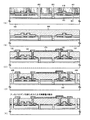
本発明の実施の形態について図1、2を用いて説明する。なお、図1、2に示したのは画素部における作製工程を示す断面図である。また、本実施の形態によって作製される画素の上面図を図3に示す。図3に用いた符号は図1、2で用いた符号に対応している。
【0013】
図1(A)において、101は素子が形成される基板(以下、素子形成基板という)であり、その上には非晶質シリコン膜からなる剥離層102が100〜500nm(本実施の形態では300nm)の厚さに形成される。本実施の形態では素子形成基板101としてガラス基板を用いるが、石英基板、シリコン基板、金属基板もしくはセラミックス基板を用いても構わない。なお、本明細書中では、半導体素子もしくは発光素子が形成された基板全体を指して素子形成基板と呼ぶ場合もある。
【0014】
また、剥離層102の成膜は減圧熱CVD法、プラズマCVD法、スパッタ法もしくは蒸着法を用いれば良い。剥離層102の上には酸化シリコン膜からなる絶縁膜103が200nmの厚さに形成される。絶縁膜103の形成は減圧熱CVD法、プラズマCVD法、スパッタ法もしくは蒸着法を用いれば良い。
【0015】
また、絶縁膜103の上には結晶質シリコン膜104が50nmの厚さに形成される。結晶質シリコン膜104の形成方法としては公知の手段を用いることが可能である。固体レーザーもしくはエキシマレーザーを用いて非晶質シリコン膜をレーザー結晶化させても良いし、非晶質シリコン膜を加熱処理(ファーネスアニール)により結晶化させても良い。
【0016】
次に、図1(B)に示すように、結晶質シリコン膜104をパターニングして島状の結晶質シリコン膜(以下、活性層という)105、106を形成する。そして活性層を覆って酸化シリコン膜からなるゲート絶縁膜107を80nmの厚さに形成する。さらに、ゲート絶縁膜107の上にゲート電極108、109を形成する。本実施の形態ではゲート電極108、109の材料として、350nm厚のタングステン膜もしくはタングステン合金膜を用いる。勿論、ゲート電極の材料としては他の公知の材料を用いることができる。
【0017】
そして、ゲート電極108、109をマスクとして周期表の13族に属する元素(代表的にはボロン)を添加する。添加方法は公知の手段を用いれば良い。こうしてp型の導電型を示す不純物領域(以下、p型不純物領域という)110〜114が形成される。また、ゲート電極の直下にはチャネル形成領域115〜117が画定する。なお、p型不純物領域110〜114はTFTのソース領域もしくはドレイン領域となる。
【0018】
次に、図1(C)に示すように、窒化シリコン膜118を50nmの厚さに形成し、その後、加熱処理を行って添加された周期表の13族に属する元素の活性化を行う。この活性化はファーネスアニール、レーザーアニールもしくはランプアニールにより行うか、又はそれらを組み合わせて行えば良い。本実施の形態では500℃4時間の加熱処理を窒素雰囲気で行う。
【0019】
活性化が終了したら、水素化処理を行うと効果的である。水素化処理は公知の水素アニール技術もしくはプラズマ水素化技術を用いれば良い。
【0020】
次に、図1(D)に示すように、酸化シリコン膜からなる第1層間絶縁膜119を800nmの厚さに形成し、コンタクトホールを形成して配線120〜123を形成する。第1層間絶縁膜119としては他の無機絶縁膜を用いても良いし、樹脂(有機絶縁膜)を用いても良い。本実施の形態では配線120〜123としてチタン/アルミニウム/チタンの三層構造からなる金属配線を用いる。勿論、導電膜であれば如何なる材料を用いても良い。配線120〜123はTFTのソース配線もしくはドレイン配線となる。
【0021】
この状態でスイッチング用TFT201及び電流制御用TFT(駆動用TFT)202が完成する。本実施の形態ではどちらのTFTもpチャネル型TFTで形成される。但し、スイッチング用TFT201はゲート電極が活性層を二カ所で横切るように形成されており、二つのチャネル形成領域が直列に接続された構造となっている。このような構造とすることでオフ電流値(TFTがオフされた時に流れる電流)を効果的に抑制することができる。
【0022】
また、同時に図3(A)、(B)に示すように保持容量301が形成される。
保持容量301は活性層と同時に形成された半導体層302、ゲート絶縁膜107及びゲート電極109で形成される下側保持容量と、ゲート電極109、第1層間絶縁膜119及び配線123で形成される上側保持容量とで形成される。また、半導体層302は配線123と電気的に接続されている。
【0023】
次に、図1(D)に示すように、透明導電膜(代表的には酸化インジウムと酸化スズとの化合物膜)を100nmの厚さに形成し、パターニングにより画素電極124を形成する。このとき、配線122と画素電極124とはオーミック接触をする。従って、画素電極124と電流制御用TFT202とは電気的に接続される。また、画素電極124はEL素子の陽極として機能する。
【0024】
画素電極124を形成したら、酸化シリコン膜からなる第2層間絶縁膜125を300nmの厚さに形成する。そして、開口部126を形成し、70nm厚の有機EL層127及び300nm厚の陰極128を蒸着法により形成する。本実施の形態では有機EL層127として20nm厚の正孔注入層及び50nm厚の発光層を積層した構造を用いる。勿論、発光層に正孔注入層、正孔輸送層、電子輸送層もしくは電子注入を組み合わせた公知の他の構造を用いても良い。
【0025】
本実施の形態では、正孔注入層としてCuPc(銅フタロシアニン)を用いる。この場合、まず全ての画素電極を覆うように銅フタロシアニンを形成し、その後、赤色、緑色及び青色に対応する画素ごとに各々赤色の発光層、緑色の発光層及び青色の発光層を形成する。形成する領域の区別は蒸着時にシャドーマスクを用いて行えば良い。このようにすることでカラー表示が可能となる。
【0026】
なお、緑色の発光層を形成する時は、発光層の母体材料としてAlq3(トリス−8−キノリノラトアルミニウム錯体)を用い、キナクリドンもしくはクマリン6をドーパントとして添加する。また、赤色の発光層を形成する時は、発光層の母体材料としてAlq3を用い、DCJT、DCM1もしくはDCM2をドーパントとして添加する。また、青色の発光層を形成する時は、発光層の母体材料としてBAlq3(2−メチル−8−キノリノールとフェノール誘導体の混合配位子を持つ5配位の錯体)を用い、ペリレンをドーパントとして添加する。
【0027】
勿論、本発明では上記有機材料に限定する必要はなく、公知の低分子系有機EL材料、高分子系有機EL材料もしくは無機EL材料を用いることが可能である。高分子系有機EL材料を用いる場合は塗布法を用いることもできる。
【0028】
また、一重項励起を経由する発光性材料だけでなく三重項励起を経由する発光性材料を用いることも可能である。即ち、蛍光を発光する発光性材料だけでなく燐光を発光する発光性材料を用いることも可能である。
【0029】
以上のようにして、画素電極(陽極)124、有機EL層127及び陰極128からなるEL素子(図3(B)において305で示される)が形成される。本実施の形態ではこのEL素子が発光素子として機能する。
【0030】
次に、図2(A)に示すように、第1接着剤129により素子を固定するための基板(以下、固定基板という)130を貼り合わせる。本実施の形態では固定基板130として可撓性のプラスチックフィルムを用いるが、ガラス基板、石英基板、プラスチック基板、シリコン基板もしくはセラミックス基板を用いても良い。また、第1接着剤129としては、後に剥離層102を除去する際に選択比のとれる材料を用いる必要がある。
【0031】
代表的には樹脂からなる絶縁膜を用いることができ、本実施の形態ではポリイミドを用いるが、アクリル、ポリアミドもしくはエポキシ樹脂を用いても良い。なお、EL素子から見て観測者側(表示装置の使用者側)に位置する場合は、光を透過する材料であることが必要である。
【0032】
図2(A)のプロセスを行うことによりEL素子を完全に大気から遮断することができる。これにより酸化による有機EL材料の劣化をほぼ完全に抑制することができ、EL素子の信頼性を大幅に向上させることができる。
【0033】
次に、図2(B)に示すように、EL素子の形成された基板全体を、フッ化ハロゲンを含むガス中に晒し、剥離層102の除去を行う。本実施の形態ではフッ化ハロゲンとして三フッ化塩素(ClF3)を用い、希釈ガスとして窒素を用いる。希釈ガスとしては、アルゴン、ヘリウムもしくはネオンを用いても良い。流量は共に500sccm(8.35×10⁻⁶m3/s)とし、反応圧力は1〜10Torr(1.3×102〜1.3×103Pa)とすれば良い。また、処理温度は室温(典型的には20〜27℃)で良い。
【0034】
この場合、シリコン膜はエッチングされるが、プラスチックフィルム、ガラス基板、ポリイミド膜、酸化シリコン膜はエッチングされない。即ち、三フッ化塩素ガスに晒すことで剥離層102が選択的にエッチングされ、最終的には完全に除去される。なお、同じくシリコン膜で形成されている活性層105、106はゲート絶縁膜107に覆われているため三フッ化塩素ガスに晒されることがなく、エッチングされることはない。
【0035】
本実施の形態の場合、剥離層102は露呈した端部から徐々にエッチングされていき、完全に除去された時点で素子形成基板101と絶縁膜103が分離される。このとき、TFT及びEL素子は薄膜を積層して形成されているが、固定基板130に移された形で残る。
【0036】
なお、ここでは剥離層102が端部からエッチングされていくことになるが、素子形成基板101が大きくなると完全に除去されるまでの時間が長くなり好ましいものではない。従って、本実施の形態は素子形成基板101が対角3インチ以下(好ましくは対角1インチ以下)の場合に実施することが望ましい。
【0037】
こうして固定基板130にTFT及びEL素子を移したら、図2(C)に示すように、第2接着剤131を形成し、プラスチックフィルム132を貼り合わせる。第2接着剤131としては樹脂からなる絶縁膜(代表的にはポリイミド、アクリル、ポリアミドもしくはエポキシ樹脂)を用いても良いし、無機絶縁膜(代表的には酸化シリコン膜)を用いても良い。なお、EL素子から見て観測者側に位置する場合は、光を透過する材料であることが必要である。
【0038】
こうしてガラス基板101からプラスチックフィルム132へとTFT及びEL素子が移される。その結果、二枚のプラスチックフィルム130、132によって挟まれたフレキシブルなEL表示装置を得ることができる。このように固定基板(ここではプラスチックフィルム)130と貼り合わせ基板(ここではプラスチックフィルム)132を同一材料とすると熱膨張係数が等しくなるので、温度変化による応力歪みの影響を受けにくくすることができる。
【0039】
本実施の形態により作製されたEL表示装置は、フォトリソグラフィに必要なマスク枚数がトータルで6枚と非常に少なく、高い歩留まりと低い製造コストを達成することができる。また、こうして形成されたEL表示装置は、プラスチック支持体の耐熱性に制限されることなく形成されたTFTを半導体素子として用いることができるので非常に高性能なものとすることができる。
【0040】
【実施例】
〔実施例1〕
本実施例では実施の形態とは異なる作製方法でEL表示装置を作製した場合の例について説明する。まず、実施の形態の説明に従って、図1(C)の状態を得る。窒化シリコン膜118を形成した後、その上にレジスト401を形成する。そして、レジスト401をマスクとして窒化シリコン膜118、ゲート絶縁膜107、絶縁膜103、剥離層102を順次エッチングし、素子形成基板101に達する開口部402、403を形成する。(図4(A))
【0041】
次に、図4(B)に示すように、レジスト401を除去した後に樹脂からなる第1層間絶縁膜404を形成する。本実施例では第1層間絶縁膜404として2μmの厚さのポリイミド膜を用いる。このとき、開口部402、403の底部にて素子形成基板101と第1層間絶縁膜404とが接着される。
【0042】
次に、図4(C)に示すように、第1層間絶縁膜404にコンタクトホールを形成し、配線120〜123を形成する。さらに、透明導電膜からなる画素電極124を形成する。これらの配線及び電極の形成は実施の形態と同様である。
【0043】
画素電極124を形成したら、次は図4(D)に示すように、第1層間絶縁膜404、窒化シリコン膜118、ゲート絶縁膜107、絶縁膜103を順次エッチングし、剥離層102に達する開口部405、406を形成する。
【0044】
次に、図4(E)に示すように、TFTの形成された基板全体を、フッ化ハロゲンを含むガス中に晒し、剥離層102の除去を行う。本実施例ではフッ化ハロゲンとして三フッ化塩素(ClF3)を用い、希釈ガスとして窒素を用いる。流量は共に500sccm(8.35×10⁻⁶m3/s)とし、反応圧力は10Torr(1.3×103Pa)とする。また、処理温度は25℃とする。
【0045】
本実施例の場合、開口部405、406からも三フッ化塩素ガスが侵入するため端部だけでなく基板面の内部からも剥離層102のエッチングが進行する。従って、実施の形態で説明した場合に比べて剥離層102の除去工程のスループットを向上させることができる。勿論、剥離層102以外の薄膜は三フッ化塩素ガスにエッチングされることはなく、シリコン膜からなる活性層も酸化シリコン膜に保護されてエッチングされない。
【0046】
このようにして剥離層102の除去工程を行うと、図4(E)に示すように開口部402、403の底部にて第1層間絶縁膜404により素子形成基板101が接着された状態となる。実際には、図6に示すように画素の各所に開口部402、403が形成されるため十分な強度で接着しておくことが可能である。また、本実施例に従えば素子形成基板101が対角3インチ以上であっても十分に本発明を実施することが可能である。
【0047】
次に、図5(A)に示すように、開口部126を設けた第2層間絶縁膜407を形成する。第2層間絶縁膜407は開口部405、406を塞ぐ効果も果たしている。さらに、有機EL層127及び陰極128を形成してEL素子が完成する。有機EL層127及び陰極128の材料、構造もしくは形成方法に関しては実施の形態の説明を参照すれば良い。
【0048】
次に、図5(B)に示すように、第1接着剤(本実施例ではエポキシ樹脂)129により固定基板130を貼り合わせる。また、本実施例では固定基板130としてプラスチック基板を用いる。これよりEL素子を完全に大気から遮断することができる。
【0049】
次に、開口部402、403の底部にて接着された素子形成基板101と第1層間絶縁膜404とを分離する。この工程は機械的に行っても良いし、加熱処理を行って分離することも可能である。
【0050】
素子形成基板101と第1層間絶縁膜404とを分離したら、第2接着剤131を用いて貼り合わせ基板132を貼り合わせる。本実施例では第2接着剤131としてポリイミド膜を用い、貼り合わせ基板132としてプラスチック基板を用いる。このように固定基板130と貼り合わせ基板132を同一材料とすると熱膨張係数が等しくなるので、温度変化による応力歪みの影響を受けにくくすることができる。
【0051】
本実施の形態により作製されたEL表示装置は、フォトリソグラフィに必要なマスク枚数がトータルで6枚と非常に少なく、高い歩留まりと低い製造コストを達成することができる。また、こうして形成されたEL表示装置は、プラスチック支持体の耐熱性に制限されることなく形成されたTFTを半導体素子として用いることができるので非常に高性能なものとすることができる。
【0052】
〔実施例2〕
発明の実施の形態もしくは実施例1において、ゲート電極を形成するところまでの作製工程として本出願人による特開平9−312260号公報、特開平10−247735号公報、特開平10−270363号公報もしくは特開平11−191628号公報のいずれかに記載の発明を用いることは有効である。
【0053】
上記公報に記載された技術はいずれも非常に高い結晶性を有する結晶質シリコン膜を形成するための技術であり、これらの技術を用いることで高性能なTFTを形成することが可能である。これらの技術はいずれも550℃以上の加熱処理を含むが、本発明の技術を用いることで、素子形成基板として耐熱性の低いプラスチック支持体を用いることが可能となる。
【0054】
なお、本実施例の構成は、発明の実施の形態もしくは実施例1の構成と自由に組み合わせて実施することが可能である。
【0055】
〔実施例3〕
本実施例では本発明を液晶表示装置に用いた場合の例について説明する。説明には図7を用いる。
【0056】
図7(A)において、701はガラスからなる素子形成基板、702は非晶質シリコンからなる剥離層、703は窒化酸化シリコンからなる絶縁膜、704は画素TFTである。画素TFT704は発明の実施の形態に説明した工程に従って作製されたpチャネル型TFTであり、本実施例では液晶に加えられる電圧を制御するためのスイッチング素子として用いる。また、705は画素TFT704に電気的に接続された透明導電膜からなる画素電極である。
【0057】
以上に説明した構造までは発明の実施の形態で説明した作製工程に従えば良い。勿論、TFTの構造はボトムゲート型であっても良いし、TFTの作製工程は発明の実施の形態で説明した工程に限定する必要はない。
【0058】
画素TFT704及び画素電極705を形成したら、樹脂からなる配向膜706を形成する。配向膜706は印刷法により形成すれば良い。また、膜厚は60nmとする。
【0059】
次に、プラスチックフィルムからなる対向基板707を用意し、その上にチタンからなる遮光膜708を120nmの厚さに、透明導電膜からなる対向電極709を110nmの厚さに形成する。その上には配向膜710を60nmの厚さに形成する。
【0060】
次に、素子形成基板側の配向膜706の上にシール剤(図示せず)をディスペンサー等の手段により形成し、素子形成基板側の配向膜706と対向基板側の配向膜710とを向かい合わせて貼り合わせ、加圧プレスして接着する。さらに、シール材に囲まれた領域に真空注入法を用いて液晶711を注入し、シール材の注入口を樹脂で塞いで液晶セルを完成させる。これらの工程は公知の液晶セルの作製工程を実施すれば良い。
【0061】
このとき、図示しないシール材としてはポリイミド、アクリルもしくはエポキシ樹脂を用いるが、後に剥離層702をエッチングする際に選択比を確保しうる材料を用いることが必要である。このシール剤は図2(A)の第1接着剤129と同様の役割を果たす。
【0062】
次に、図7(B)に示すように、フッ化ハロゲンを含むガス中に液晶セル全体を晒し、剥離層702をエッチングする。本実施例ではフッ化ハロゲンとして三フッ化塩素を用い、希釈ガスとしてアルゴンを用いる。なお、本実施例では剥離層が素子形成基板701で覆われた状態で処理を行うため剥離層702の露呈面から徐々にエッチングされる。
【0063】
こうして最終的には剥離層702が完全に除去され、窒化酸化シリコンからなる絶縁膜703が露呈する。このとき、対向基板707が素子の形状を固定する固定基板として機能する。
【0064】
最後に、アクリル膜からなる第2接着剤712を用いて貼り合わせ基板713を接着する。本実施例では、貼り合わせ基板713としてプラスチックフィルムを用いる。勿論、プラスチック基板を用いても構わない。
【0065】
以上のように、本発明を液晶表示装置に用いる場合は液晶の注入工程までを完了させて一旦液晶表示装置を完成させ、その後に対向基板を固定基板として利用しつつ剥離層の除去工程を行うことができる。そのため、特に煩雑な工程を増やすことなく、高性能なTFTをプラスチック支持体の上に形成できる。
【0066】
なお、実施例1で説明した方法により液晶を注入する前に素子形成基板と貼り合わせ基板とを張り替えることも可能である。その場合、実施例1の構成と本実施例の構成とを組み合わせれば容易に実施することができる。また、実施例2の構成を組み合わせても構わない。
【0067】
〔実施例4〕
本実施例では本発明を単純マトリクス型EL表示装置に用いた場合の例について説明する。説明には図8を用いる。
【0068】
図8(A)において、801はガラスからなる素子形成基板、802は非晶質シリコンからなる剥離層、803は窒化酸化シリコンからなる絶縁膜、804は第1ストライプ電極であり、本実施例では透明導電膜からなる陽極である。この陽極804は紙面と平行な方向にストライプ状に複数本形成されている。
【0069】
第1ストライプ電極804上には素子分離用絶縁膜805及び樹脂膜からなるバンク806がストライプ状に複数本形成される。これらは前述の第1ストライプ電極804と直交するように形成される。こうして素子分離用絶縁膜805及び樹脂膜からなるバンク806を形成したら、有機EL層807、第2ストライプ電極(本実施例では金属膜からなる陰極)808を蒸着法により形成する。第2ストライプ電極808はバンク806によってストライプ状に分離されて形成されるため、第1ストライプ電極804と直交するように形成される。
【0070】
この時、第1ストライプ電極(ここでは陽極)804、有機EL層807及び第2ストライプ電極(ここでは陰極)808で形成されるコンデンサがEL素子となる。勿論、第1ストライプ電極804、有機EL層807及び第2ストライプ電極808の形成方法もしくは形成材料は公知のものを用いることができる。
【0071】
EL素子が形成されたら、第1接着剤(本実施例ではアクリル)809を用いてプラスチックフィルム810を接着する。こうしてEL素子が完全に大気から遮断された状態とすることができる。
【0072】
次に、EL素子の形成された基板を、三フッ化塩素ガスを含む窒素雰囲気に晒し、剥離層802をエッチングして除去する。そして、EL素子と素子形成基板801とを分離させる。
【0073】
次に、第2接着剤811を用いて貼り合わせ基板812を接着する。本実施例では第2接着剤811としてポリイミド膜を用い、貼り合わせ基板812としてプラスチックフィルムを用いる。
【0074】
本実施の形態により作製されたEL表示装置は、フォトリソグラフィに必要なマスク枚数がトータルで2枚と非常に少なく、高い歩留まりと低い製造コストを達成することができる。なお、本実施例の構成は実施例2と組み合わせて実施することも可能である。
【0075】
〔実施例5〕
本実施例では、貼り合わせ基板に予めカラーフィルタを設けて貼り合わせる場合について図9を用いて説明する。
【0076】
まず、実施例2に従って図5(A)の状態を得る。但し、本実施例では有機EL層127の代わりに白色発光の有機EL層901を形成する。具体的には、発光層として、特開平8−96959号公報または特開平9−63770号公報に記載された材料を用いれば良い。本実施例では発光層として1,2−ジクロロメタンに、PVK(ポリビニルカルバゾール)、Bu−PBD(2−(4'−tert−ブチルフェニル)−5−(4''−ビフェニル)−1,3,4−オキサジアゾール)、クマリン6、DCM1(4−ジシアノメチレン−2−メチル−6−p−ジメチルアミノスチリル−4H−ピラン)、TPB(テトラフェニルブタジエン)、ナイルレッドを溶解したものを用いる。また、有機EL層901の上にはアルミニウムとリチウムとの合金膜からなる陰極902を形成する。
【0077】
次に、図9(B)に示すように、第1接着剤(本実施例ではポリイミド膜)903を用いて固定基板(本実施例ではプラスチックフィルム)904を貼り合わせる。そして、素子形成基板101を分離する。
【0078】
次に、図9(C)に示すように、赤色に対応するカラーフィルタ905、緑色に対応するカラーフィルタ906及び青色に対応するカラーフィルタ907を設けた貼り合わせ基板(本実施例ではプラスチックフィルム)を、第2接着剤(本実施例ではエポキシ樹脂)909を用いて貼り合わせる。
【0079】
このとき、各カラーフィルタはスピンコート法とフォトリソグラフィ技術との組み合わせもしくは印刷法を用いて形成することができるため、問題なくプラスチックフィルム上に形成することができる。また、素子形成基板上にカラーフィルタを形成する場合に比べて、歩留まりの向上が期待できる。
【0080】
なお、本実施例の構成は、発明の実施の形態もしくは実施例1〜4の構成と自由に組み合わせて実施することが可能である。
【0081】
〔実施例6〕
本発明において、固定基板及び/又は貼り合わせ基板の片面もしくは両面にDLC(ダイヤモンドライクカーボン)膜を形成しておくことは有効である。但し、膜厚が厚すぎると透過率が落ちるので、50nm以下(好ましくは10〜20nm)とすると良い。
【0082】
DLC膜の特徴としては、1550cm-1くらいに非対称のピークを有し、1300cm-1くらいに肩をもつラマンスペクトル分布を有する。また、微小硬度計で測定した時に15〜25Paの硬度を示すという特徴をもつ。
【0083】
DLC膜はプラスチック支持体に比べて硬度が大きく、熱伝導率も大きいため、表面保護のための保護膜として設けておくことが有効である。
【0084】
従って、プラスチック支持体を貼り付ける前に予めDLC膜を成膜しておいて貼り付けるか、プラスチック支持体を貼り付けた後にDLC膜を成膜することも可能である。いずれにしてもDLC膜の成膜はスパッタ法もしくはECRプラズマCVD法を用いれば良い。
【0085】
なお、本実施例の構成は実施例1〜5のいずれの構成とも自由に組み合わせて実施することが可能である。
【0086】
〔実施例7〕
実施例1、2、4〜6ではEL素子を用いた表示装置を例にして説明してきたが、本発明はEC(エレクトロクロミクス)表示装置、フィールドエミッションディスプレイ(FED)または半導体を用いた発光ダイオードを有する表示装置に用いることも可能である。
【0087】
【発明の効果】
本発明では、半導体素子の作製過程においてプラスチックよりも耐熱性の高い基板(素子形成基板)を用いるため、電気特性の高い半導体素子を作製することができる。さらに、半導体素子及び発光素子を形成した後で前記素子形成基板を剥離し、プラスチック支持体を貼り合わせる。
【0088】
そのため、プラスチック支持体を支持基板とし、且つ、高性能な表示装置を作製することが可能となる。また、支持基板がプラスチックであるため、フレキシブルな表示装置にすることもでき、且つ、軽量な表示装置とすることが可能である。
【図面の簡単な説明】
【図1】 EL表示装置の作製工程を示す図。
【図2】 EL表示装置の作製工程を示す図。
【図3】 EL表示装置の上面構造及び回路構成を示す図。
【図4】 EL表示装置の作製工程を示す図。
【図5】 EL表示装置の作製工程を示す図。
【図6】 EL表示装置の上面構造を示す図。
【図7】 液晶表示装置の作製工程を示す図。
【図8】 EL表示装置の作製工程を示す図。
【図9】 EL表示装置の作製工程を示す図。[0001]
BACKGROUND OF THE INVENTION
The present invention relates to a device having an element (hereinafter referred to as a light emitting device) having a luminescent material sandwiched between electrodes (hereinafter referred to as a light emitting device) or a device having an element (hereinafter referred to as liquid crystal element) having a liquid crystal sandwiched between electrodes. The present invention relates to a manufacturing method (hereinafter referred to as a liquid crystal display device). Note that the light emitting device and the liquid crystal display device are collectively referred to as a display device.
[0002]
The luminescent material includes all luminescent materials that emit light (phosphorescence and / or fluorescence) via singlet excitation, triplet excitation, or both excitation.
[0003]
[Prior art]
In recent years, development of a light emitting device (hereinafter referred to as an EL display device) using a light emitting element (hereinafter referred to as an EL element) using a light emitting material (hereinafter referred to as an EL material) from which EL (Electro Luminescence) can be obtained has been advanced. Yes. The EL display device has a structure having an EL element having an EL material sandwiched between an anode and a cathode. By applying a voltage between the anode and the cathode and passing a current through the EL material, carriers are recombined to emit light. That is, since the EL display device has a light emission capability, the backlight used in the liquid crystal display device is unnecessary. Furthermore, it has the advantages of a wide viewing angle, light weight, and low power consumption.
[0004]
Various applications using such an EL display device are expected. However, the use of the EL display device in a portable device is attracting attention because the thickness of the EL display device is thin, and thus the weight can be reduced. . Therefore, it has been attempted to form a light emitting element on a flexible plastic film.
[0005]
However, since the heat resistance of the plastic film is low, the maximum temperature of the process has to be lowered, and as a result, TFTs having better electrical characteristics cannot be formed than when formed on a glass substrate. Therefore, a high-performance display device using a plastic film has not been realized.
[0006]
[Problems to be solved by the invention]
An object of the present invention is to provide a technique for manufacturing a high-performance display device using a plastic support (including a flexible plastic film or a plastic substrate).
[0007]
[Means for Solving the Problems]
In the present invention, necessary elements are formed on a substrate (glass substrate, quartz substrate, silicon substrate, metal substrate, or ceramic substrate) that is more heat resistant than plastic, and these elements are then supported by processing at room temperature. It is characterized by being transferred to the body.
[0008]
Note that the necessary elements refer to semiconductor elements (typically thin film transistors) or MIM elements and light-emitting elements or liquid crystal elements used as pixel switching elements in an active matrix display device. A passive display device refers to a light-emitting element or a liquid crystal element. As the plastic support, PES (polyethylene sulfide), PC (polycarbonate), PET (polyethylene terephthalate) or PEN (polyethylene naphthalate) can be used.
[0009]
In the present invention, the element is formed on a release layer made of a silicon film (including a silicon germanium film), and the release layer is removed using a gas containing halogen fluoride in the final step. As a result, each element and the substrate are separated, and thereafter, the element can be bonded to the plastic support. Etching of the silicon film with halogen fluoride easily proceeds at room temperature, and thus can be performed without any problem even after a light-emitting element with low heat resistance is formed.
[0010]
Halogen fluoride is a substance represented by the chemical formula XFn (where X is a halogen other than fluorine, and n is an integer). Chlorine monofluoride (ClF), chlorine trifluoride (ClF) Three ), Bromine monofluoride (BrF), bromine trifluoride (BrF) Three ), Iodine monofluoride (IF) or iodine trifluoride (IF Three ) Can be used. The silicon film may be a crystalline silicon film or an amorphous silicon film. This halogen fluoride has a large selection ratio between the silicon film and the silicon oxide film, and can selectively etch the silicon film.
[0011]
The silicon film is etched only by exposing the silicon film to the above-mentioned halogen fluoride. However, even if other fluorides (carbon tetrafluoride (CF4) or nitrogen trifluoride) are used, the silicon film is brought into a plasma state. It can be used in the present invention.
[0012]
DETAILED DESCRIPTION OF THE INVENTION
An embodiment of the present invention will be described with reference to FIGS. 1 and 2 are cross-sectional views showing a manufacturing process in the pixel portion. A top view of a pixel manufactured according to this embodiment mode is shown in FIG. The codes used in FIG. 3 correspond to the codes used in FIGS.
[0013]
In FIG. 1A,
[0014]
In addition, the
[0015]
On the
[0016]
Next, as shown in FIG. 1B, the
[0017]
Then, an element (typically boron) belonging to Group 13 of the periodic table is added using the
[0018]
Next, as shown in FIG. 118 Then, the element belonging to Group 13 of the periodic table is activated by heat treatment. This activation may be performed by furnace annealing, laser annealing or lamp annealing, or a combination thereof. In this embodiment, heat treatment at 500 ° C. for 4 hours is performed in a nitrogen atmosphere.
[0019]
When the activation is completed, it is effective to perform a hydrogenation treatment. For the hydrogenation treatment, a known hydrogen annealing technique or plasma hydrogenation technique may be used.
[0020]
Next, as shown in FIG. 1D, a first
[0021]
In this state, the switching
[0022]
At the same time, a
The
[0023]
Next, as shown in FIG. 1D, a transparent conductive film (typically a compound film of indium oxide and tin oxide) is formed to a thickness of 100 nm, and a
[0024]
After the
[0025]
In this embodiment, CuPc (copper phthalocyanine) is used as the hole injection layer. In this case, first, copper phthalocyanine is formed so as to cover all the pixel electrodes, and then a red light emitting layer, a green light emitting layer, and a blue light emitting layer are formed for each pixel corresponding to red, green, and blue. The regions to be formed may be distinguished using a shadow mask during vapor deposition. In this way, color display is possible.
[0026]
When forming a green light emitting layer, Alq is used as the base material of the light emitting layer. Three (Tris-8-quinolinolato aluminum complex) is used and quinacridone or coumarin 6 is added as a dopant. When a red light emitting layer is formed, Alq is used as a base material of the light emitting layer. Three And DCJT, DCM1 or DCM2 is added as a dopant. When a blue light emitting layer is formed, BAlq is used as a base material of the light emitting layer. Three (5-coordinate complex having a mixed ligand of 2-methyl-8-quinolinol and a phenol derivative) and perylene is added as a dopant.
[0027]
Of course, in the present invention, it is not necessary to limit to the above organic material, and it is possible to use a known low molecular organic EL material, high molecular organic EL material, or inorganic EL material. When using a polymer organic EL material, a coating method can also be used.
[0028]
Moreover, it is possible to use not only a light-emitting material that passes through singlet excitation but also a light-emitting material that passes through triplet excitation. That is, not only a luminescent material that emits fluorescence but also a luminescent material that emits phosphorescence can be used.
[0029]
As described above, an EL element (indicated by 305 in FIG. 3B) including the pixel electrode (anode) 124, the
[0030]
Next, as shown in FIG. 2A, a substrate (hereinafter, referred to as a fixed substrate) 130 for fixing the element with a
[0031]
Typically, an insulating film made of a resin can be used, and polyimide is used in this embodiment mode, but acrylic, polyamide, or epoxy resin may be used. In addition, when located on the observer side (the user side of the display device) as viewed from the EL element, it is necessary to be a material that transmits light.
[0032]
By performing the process of FIG. 2A, the EL element can be completely shielded from the atmosphere. Thereby, deterioration of the organic EL material due to oxidation can be suppressed almost completely, and the reliability of the EL element can be greatly improved.
[0033]
Next, as illustrated in FIG. 2B, the entire substrate on which the EL element is formed is exposed to a gas containing halogen fluoride, and the
[0034]
In this case, the silicon film is etched, but the plastic film, glass substrate, polyimide film, and silicon oxide film are not etched. That is, the
[0035]
In the case of this embodiment mode, the
[0036]
Note that the
[0037]
When the TFT and the EL element are transferred to the fixed
[0038]
Thus, the TFT and the EL element are transferred from the
[0039]
In the EL display device manufactured according to this embodiment mode, the total number of masks necessary for photolithography is as very small as six, and a high yield and a low manufacturing cost can be achieved. In addition, the EL display device thus formed can have a very high performance because a TFT formed without being limited by the heat resistance of the plastic support can be used as a semiconductor element.
[0040]
【Example】
[Example 1]
In this example, an example in which an EL display device is manufactured by a manufacturing method different from that in Embodiment Mode will be described. First, according to the description of the embodiment, the state of FIG. After the
[0041]
Next, as shown in FIG. 4B, after the resist 401 is removed, a first
[0042]
Next, as shown in FIG. 4C, contact holes are formed in the first
[0043]
After the
[0044]
Next, as illustrated in FIG. 4E, the entire substrate on which the TFT is formed is exposed to a gas containing halogen fluoride, and the
[0045]
In this embodiment, the chlorine trifluoride gas also enters from the
[0046]
When the
[0047]
Next, as shown in FIG. 5A, a second
[0048]
Next, as shown in FIG. 5B, the fixed
[0049]
Next, the
[0050]
After the
[0051]
In the EL display device manufactured according to this embodiment mode, the total number of masks necessary for photolithography is as very small as six, and a high yield and a low manufacturing cost can be achieved. In addition, the EL display device thus formed can have a very high performance because a TFT formed without being limited by the heat resistance of the plastic support can be used as a semiconductor element.
[0052]
[Example 2]
In the embodiment of the invention or Example 1, as a manufacturing process up to the formation of the gate electrode, Japanese Patent Laid-Open No. 9-31260, Japanese Patent Laid-Open No. 10-247735, Japanese Patent Laid-Open No. 10-270363, or It is effective to use the invention described in any one of JP-A-11-191628.
[0053]
All of the techniques described in the above publications are techniques for forming a crystalline silicon film having very high crystallinity, and high performance TFTs can be formed by using these techniques. All of these techniques include heat treatment at 550 ° C. or higher, but by using the technique of the present invention, it becomes possible to use a plastic support having low heat resistance as the element formation substrate.
[0054]
Note that the configuration of this example can be implemented by freely combining with the configuration of the embodiment of the invention or Example 1.
[0055]
Example 3
In this embodiment, an example in which the present invention is used in a liquid crystal display device will be described. FIG. 7 is used for the description.
[0056]
7A,
[0057]
The manufacturing process described in the embodiment mode may be followed up to the structure described above. Needless to say, the structure of the TFT may be a bottom gate type, and the manufacturing process of the TFT is not necessarily limited to the process described in the embodiment of the invention.
[0058]
After the
[0059]
Next, a
[0060]
Next, a sealing agent (not shown) is formed on the
[0061]
At this time, polyimide, acrylic, or epoxy resin is used as a sealing material (not shown), but it is necessary to use a material that can secure a selection ratio when the
[0062]
Next, as shown in FIG. 7B, the entire liquid crystal cell is exposed to a gas containing halogen fluoride, and the
[0063]
In this way, finally, the
[0064]
Finally, from the acrylic film Become The bonded
[0065]
As described above, when the present invention is used for a liquid crystal display device, the liquid crystal display device is completed by completing the liquid crystal injection step, and then the peeling layer removing step is performed using the counter substrate as a fixed substrate. be able to. Therefore, a high-performance TFT can be formed on the plastic support without increasing particularly complicated processes.
[0066]
Note that the element formation substrate and the bonded substrate can be replaced before the liquid crystal is injected by the method described in Embodiment 1. In that case, it can be easily implemented by combining the configuration of the first embodiment and the configuration of the present embodiment. Moreover, you may combine the structure of Example 2. FIG.
[0067]
Example 4
In this embodiment, an example in which the present invention is used in a simple matrix EL display device will be described. FIG. 8 is used for the description.
[0068]
In FIG. 8A, 801 is an element formation substrate made of glass, 802 is a release layer made of amorphous silicon, 803 is an insulating film made of silicon nitride oxide, and 804 is a first stripe electrode. An anode made of a transparent conductive film. A plurality of
[0069]
On the
[0070]
At this time, a capacitor formed by the first stripe electrode (here, anode) 804, the
[0071]
When the EL element is formed, the
[0072]
Next, the substrate over which the EL element is formed is exposed to a nitrogen atmosphere containing chlorine trifluoride gas, and the
[0073]
Next, the bonded
[0074]
In the EL display device manufactured according to this embodiment mode, the total number of masks required for photolithography is as few as two, and a high yield and a low manufacturing cost can be achieved. The configuration of this embodiment can be implemented in combination with the second embodiment.
[0075]
Example 5
In this embodiment, a case where a color filter is provided over a bonded substrate in advance and bonded is described with reference to FIG.
[0076]
First, the state shown in FIG. However, in this embodiment, a white light emitting
[0077]
Next, as shown in FIG. 9B, a fixed substrate (a plastic film in this embodiment) 904 is bonded using a first adhesive (a polyimide film in this embodiment) 903. Then, the
[0078]
Next, as shown in FIG. 9C, a bonded substrate (a plastic film in this embodiment) provided with a
[0079]
At this time, each color filter can be formed on a plastic film without any problem because it can be formed by using a combination of a spin coating method and a photolithography technique or a printing method. In addition, an improvement in yield can be expected as compared with the case where a color filter is formed on an element formation substrate.
[0080]
The configuration of this example can be implemented in combination with the configuration of the embodiment of the invention or Examples 1-4.
[0081]
Example 6
In the present invention, it is effective to form a DLC (diamond-like carbon) film on one or both surfaces of the fixed substrate and / or the bonded substrate. However, if the film thickness is too thick, the transmittance decreases.
[0082]
As a feature of the DLC film, 1550cm -1 1300cm with asymmetric peaks -1 It has a Raman spectral distribution with shoulders. Moreover, it has the characteristic of showing a hardness of 15-25 Pa when measured with a micro hardness meter.
[0083]
Since the DLC film has higher hardness and higher thermal conductivity than the plastic support, it is effective to provide it as a protective film for surface protection.
[0084]
Therefore, it is possible to form a DLC film in advance before attaching the plastic support and attach it, or to apply a DLC film after attaching the plastic support. In any case, the DLC film may be formed by sputtering or ECR plasma CVD.
[0085]
In addition, the structure of a present Example can be implemented in combination with any structure of Examples 1-5 freely.
[0086]
Example 7
In Examples 1, 2, and 4-6, the display device using an EL element has been described as an example. However, the present invention is a light emission using an EC (electrochromic) display device, a field emission display (FED), or a semiconductor. It can also be used for a display device having a diode.
[0087]
【The invention's effect】
In the present invention, since a substrate (element formation substrate) having higher heat resistance than plastic is used in the process of manufacturing a semiconductor element, a semiconductor element having high electrical characteristics can be manufactured. Further, after forming the semiconductor element and the light emitting element, the element formation substrate is peeled off, and a plastic support is bonded.
[0088]
Therefore, a high-performance display device can be manufactured using the plastic support as a support substrate. Further, since the supporting substrate is made of plastic, a flexible display device can be obtained, and a lightweight display device can be obtained.
[Brief description of the drawings]
FIGS. 1A to 1C illustrate a manufacturing process of an EL display device. FIGS.
FIGS. 2A and 2B illustrate a manufacturing process of an EL display device. FIGS.
FIGS. 3A and 3B illustrate a top structure and a circuit structure of an EL display device. FIGS.
4A and 4B illustrate a manufacturing process of an EL display device.
FIGS. 5A and 5B illustrate a manufacturing process of an EL display device. FIGS.
FIG. 6 illustrates a top structure of an EL display device.
FIGS. 7A to 7C illustrate a manufacturing process of a liquid crystal display device. FIGS.
FIG. 8 illustrates a manufacturing process of an EL display device.
FIGS. 9A and 9B illustrate a manufacturing process of an EL display device. FIGS.
Claims (7)
前記剥離層上に第1絶縁膜を形成し、
前記第1絶縁膜に、前記第1基板に達する第1開口部を形成し、
前記第1開口部を充填しつつ、前記第1絶縁膜上に第2絶縁膜を形成し、
前記第2絶縁膜上に発光素子の第1電極を形成し、
前記第1絶縁膜及び前記第2絶縁膜に、前記剥離層に達する第2開口部を形成し、
フッ化ハロゲンを含むガスを用いて、少なくとも前記第2開口部を介して前記剥離層をエッチングし、
前記第2絶縁膜及び前記発光素子の第1電極上に第3絶縁膜を形成し、
前記発光素子の第1電極上の前記第3絶縁膜に第3開口部を形成し、
前記第3開口部に前記発光素子の発光層、及び第2電極を形成し、
前記発光素子の第2電極上に第1接着剤を用いて第2基板を貼り合わせ、
前記第2基板を貼り合わせた後に、前記第1開口部に形成された前記第2絶縁膜で接着されていた前記第1基板を分離し、前記第1絶縁膜、及び前記第1開口部に形成された前記第2絶縁膜を露出させ、
前記第1絶縁膜及び前記第2絶縁膜に第2接着剤を用いて第3基板を貼り合わせることを特徴とする発光装置の作製方法。Forming a release layer made of a silicon film on the first substrate;
Forming a first insulating film on the release layer;
Forming a first opening reaching the first substrate in the first insulating film;
Forming a second insulating film on the first insulating film while filling the first opening;
Forming a first electrode of a light emitting element on the second insulating film;
Forming a second opening reaching the release layer in the first insulating film and the second insulating film;
Etching the release layer through at least the second opening using a gas containing halogen fluoride,
Forming a third insulating film on the second insulating film and the first electrode of the light emitting device;
Forming a third opening in the third insulating film on the first electrode of the light emitting element;
Forming a light emitting layer of the light emitting element and a second electrode in the third opening;
A second substrate is bonded onto the second electrode of the light emitting element using a first adhesive,
After bonding the second substrate, the first substrate bonded with the second insulating film formed in the first opening is separated, and the first insulating film and the first opening are separated. Exposing the formed second insulating film;
A method for manufacturing a light-emitting device, wherein a third substrate is attached to the first insulating film and the second insulating film using a second adhesive.
前記剥離層上に第1絶縁膜を形成し、
前記第1絶縁膜上に半導体素子を形成し、
前記第1絶縁膜に、前記第1基板に達する第1開口部を形成し、
前記第1開口部を充填しつつ、前記第1絶縁膜上に第2絶縁膜を形成し、
前記第2絶縁膜上に、前記半導体素子に電気的に接続される発光素子の第1電極を形成し、
前記第1絶縁膜及び前記第2絶縁膜に、前記剥離層に達する第2開口部を形成し、
フッ化ハロゲンを含むガスを用いて、少なくとも前記第2開口部を介して前記剥離層をエッチングし、
前記第2絶縁膜及び前記発光素子の第1電極上に第3絶縁膜を形成し、
前記発光素子の第1電極上の前記第3絶縁膜に第3開口部を形成し、
前記第3開口部に前記発光素子の発光層、及び第2電極を形成し、
前記発光素子の第2電極上に第1接着剤を用いて第2基板を貼り合わせ、
前記第2基板を貼り合わせた後に、前記第1開口部に形成された前記第2絶縁膜で接着されていた前記第1基板を分離し、前記第1絶縁膜、及び前記第1開口部に形成された前記第2絶縁膜を露出させ、
前記第1絶縁膜及び前記第2絶縁膜に第2接着剤を用いて第3基板を貼り合わせることを特徴とする発光装置の作製方法。Forming a release layer made of a silicon film on the first substrate;
Forming a first insulating film on the release layer;
Forming a semiconductor element on the first insulating film;
Forming a first opening reaching the first substrate in the first insulating film;
Forming a second insulating film on the first insulating film while filling the first opening;
Forming a first electrode of a light emitting element electrically connected to the semiconductor element on the second insulating film;
Forming a second opening reaching the release layer in the first insulating film and the second insulating film;
Etching the release layer through at least the second opening using a gas containing halogen fluoride,
Forming a third insulating film on the second insulating film and the first electrode of the light emitting device;
Forming a third opening in the third insulating film on the first electrode of the light emitting element;
Forming a light emitting layer of the light emitting element and a second electrode in the third opening;
A second substrate is bonded onto the second electrode of the light emitting element using a first adhesive,
After bonding the second substrate, the first substrate bonded with the second insulating film formed in the first opening is separated, and the first insulating film and the first opening are separated. Exposing the formed second insulating film;
A method for manufacturing a light-emitting device, wherein a third substrate is attached to the first insulating film and the second insulating film using a second adhesive.
Priority Applications (1)
| Application Number | Priority Date | Filing Date | Title |
|---|---|---|---|
| JP2001005860A JP4748859B2 (en) | 2000-01-17 | 2001-01-15 | Method for manufacturing light emitting device |
Applications Claiming Priority (4)
| Application Number | Priority Date | Filing Date | Title |
|---|---|---|---|
| JP2000-8403 | 2000-01-17 | ||
| JP2000008403 | 2000-01-17 | ||
| JP2000008403 | 2000-01-17 | ||
| JP2001005860A JP4748859B2 (en) | 2000-01-17 | 2001-01-15 | Method for manufacturing light emitting device |
Publications (3)
| Publication Number | Publication Date |
|---|---|
| JP2001272923A JP2001272923A (en) | 2001-10-05 |
| JP2001272923A5 JP2001272923A5 (en) | 2008-01-31 |
| JP4748859B2 true JP4748859B2 (en) | 2011-08-17 |
Family
ID=26583665
Family Applications (1)
| Application Number | Title | Priority Date | Filing Date |
|---|---|---|---|
| JP2001005860A Expired - Fee Related JP4748859B2 (en) | 2000-01-17 | 2001-01-15 | Method for manufacturing light emitting device |
Country Status (1)
| Country | Link |
|---|---|
| JP (1) | JP4748859B2 (en) |
Families Citing this family (72)
| Publication number | Priority date | Publication date | Assignee | Title |
|---|---|---|---|---|
| TW548860B (en) | 2001-06-20 | 2003-08-21 | Semiconductor Energy Lab | Light emitting device and method of manufacturing the same |
| US7211828B2 (en) | 2001-06-20 | 2007-05-01 | Semiconductor Energy Laboratory Co., Ltd. | Light emitting device and electronic apparatus |
| GB2381658B (en) * | 2001-07-25 | 2004-03-03 | Lg Philips Lcd Co Ltd | Active matrix organic electroluminescent device simplifying a fabricating process and a fabricating method thereof |
| JP4166455B2 (en) | 2001-10-01 | 2008-10-15 | 株式会社半導体エネルギー研究所 | Polarizing film and light emitting device |
| US6953735B2 (en) | 2001-12-28 | 2005-10-11 | Semiconductor Energy Laboratory Co., Ltd. | Method for fabricating a semiconductor device by transferring a layer to a support with curvature |
| JP2003255858A (en) * | 2002-02-28 | 2003-09-10 | Sanyo Electric Co Ltd | Display device |
| US7164155B2 (en) | 2002-05-15 | 2007-01-16 | Semiconductor Energy Laboratory Co., Ltd. | Light emitting device |
| US7230271B2 (en) | 2002-06-11 | 2007-06-12 | Semiconductor Energy Laboratory Co., Ltd. | Light emitting device comprising film having hygroscopic property and transparency and manufacturing method thereof |
| CN100391004C (en) | 2002-10-30 | 2008-05-28 | 株式会社半导体能源研究所 | Semiconductor device and manufacturing method thereof |
| JP2004207078A (en) * | 2002-12-25 | 2004-07-22 | Seiko Epson Corp | Display panel and method for manufacturing display panel |
| TWI351548B (en) | 2003-01-15 | 2011-11-01 | Semiconductor Energy Lab | Manufacturing method of liquid crystal display dev |
| JP4801579B2 (en) * | 2003-01-15 | 2011-10-26 | 株式会社半導体エネルギー研究所 | Method for manufacturing light emitting device |
| JP4408044B2 (en) * | 2003-01-15 | 2010-02-03 | 株式会社半導体エネルギー研究所 | Method for manufacturing liquid crystal display device |
| KR101033797B1 (en) | 2003-01-15 | 2011-05-13 | 가부시키가이샤 한도오따이 에네루기 켄큐쇼 | Separating method and method for manufacturing display device using the separating method |
| US7973313B2 (en) * | 2003-02-24 | 2011-07-05 | Semiconductor Energy Laboratory Co., Ltd. | Thin film integrated circuit device, IC label, container comprising the thin film integrated circuit, manufacturing method of the thin film integrated circuit device, manufacturing method of the container, and management method of product having the container |
| JP4718784B2 (en) * | 2003-02-28 | 2011-07-06 | 株式会社半導体エネルギー研究所 | Semiconductor element peeling method and semiconductor device manufacturing method |
| JP2004281085A (en) * | 2003-03-12 | 2004-10-07 | Nippon Hoso Kyokai <Nhk> | Flexible organic el device and flexible organic el display |
| TW594210B (en) * | 2003-08-28 | 2004-06-21 | Ind Tech Res Inst | A method for manufacturing a flexible panel for FPD |
| JP4689249B2 (en) * | 2003-11-28 | 2011-05-25 | 株式会社半導体エネルギー研究所 | Method for manufacturing display device |
| US7566640B2 (en) | 2003-12-15 | 2009-07-28 | Semiconductor Energy Laboratory Co., Ltd. | Method for manufacturing thin film integrated circuit device, noncontact thin film integrated circuit device and method for manufacturing the same, and idtag and coin including the noncontact thin film integrated circuit device |
| JP5110766B2 (en) * | 2003-12-15 | 2012-12-26 | 株式会社半導体エネルギー研究所 | Method for manufacturing thin film integrated circuit device and method for manufacturing non-contact type thin film integrated circuit device |
| US7271076B2 (en) | 2003-12-19 | 2007-09-18 | Semiconductor Energy Laboratory Co., Ltd. | Manufacturing method of thin film integrated circuit device and manufacturing method of non-contact type thin film integrated circuit device |
| JP4912586B2 (en) * | 2003-12-19 | 2012-04-11 | 株式会社半導体エネルギー研究所 | Method for manufacturing thin film integrated circuit device |
| CN1697187B (en) | 2003-12-19 | 2011-05-04 | 株式会社半导体能源研究所 | Semiconductor integrated circuit, semiconductor device, and method of manufacturing semiconductor integrated circuit |
| US7566010B2 (en) | 2003-12-26 | 2009-07-28 | Semiconductor Energy Laboratory Co., Ltd. | Securities, chip mounting product, and manufacturing method thereof |
| JP4989854B2 (en) * | 2004-02-06 | 2012-08-01 | 株式会社半導体エネルギー研究所 | Method for manufacturing semiconductor device |
| WO2005076359A1 (en) | 2004-02-06 | 2005-08-18 | Semiconductor Energy Laboratory Co., Ltd. | Semiconductor device |
| JP4836465B2 (en) * | 2004-02-06 | 2011-12-14 | 株式会社半導体エネルギー研究所 | Method for manufacturing thin film integrated circuit and element substrate for thin film integrated circuit |
| WO2005076358A1 (en) | 2004-02-06 | 2005-08-18 | Semiconductor Energy Laboratory Co., Ltd. | Method for manufacturing thin film integrated circuit, and element substrate |
| KR101219748B1 (en) | 2004-03-22 | 2013-01-18 | 가부시키가이샤 한도오따이 에네루기 켄큐쇼 | Method for manufacturing integrated circuit |
| JP5030388B2 (en) * | 2004-03-22 | 2012-09-19 | 株式会社半導体エネルギー研究所 | Method for manufacturing thin film integrated circuit |
| JP5008266B2 (en) * | 2004-03-25 | 2012-08-22 | 株式会社半導体エネルギー研究所 | Method for manufacturing semiconductor device |
| KR101226260B1 (en) | 2004-06-02 | 2013-01-28 | 가부시키가이샤 한도오따이 에네루기 켄큐쇼 | A Method for manufacturing a semiconductor device |
| CN100517728C (en) * | 2004-06-24 | 2009-07-22 | 株式会社半导体能源研究所 | Manufacturing method of thin film integrated circuit |
| JP4912627B2 (en) * | 2004-06-24 | 2012-04-11 | 株式会社半導体エネルギー研究所 | Method for manufacturing thin film integrated circuit |
| JP2006049859A (en) * | 2004-06-29 | 2006-02-16 | Semiconductor Energy Lab Co Ltd | Semiconductor device and its manufacturing method |
| US7452786B2 (en) | 2004-06-29 | 2008-11-18 | Semiconductor Energy Laboratory Co., Ltd. | Method for manufacturing thin film integrated circuit, and element substrate |
| JP5041681B2 (en) * | 2004-06-29 | 2012-10-03 | 株式会社半導体エネルギー研究所 | Method for manufacturing semiconductor device |
| JP4749062B2 (en) * | 2004-07-16 | 2011-08-17 | 株式会社半導体エネルギー研究所 | Device for sealing thin film integrated circuit and method for manufacturing IC chip |
| JP5041686B2 (en) * | 2004-07-30 | 2012-10-03 | 株式会社半導体エネルギー研究所 | Method for peeling thin film integrated circuit and method for manufacturing semiconductor device |
| KR101203090B1 (en) | 2004-07-30 | 2012-11-20 | 가부시키가이샤 한도오따이 에네루기 켄큐쇼 | Method for manufacturing semiconductor device |
| JP4912641B2 (en) * | 2004-08-23 | 2012-04-11 | 株式会社半導体エネルギー研究所 | Manufacturing method of wireless chip |
| US8040469B2 (en) | 2004-09-10 | 2011-10-18 | Semiconductor Energy Laboratory Co., Ltd. | Display device, method for manufacturing the same and apparatus for manufacturing the same |
| JP4954515B2 (en) * | 2004-09-10 | 2012-06-20 | 株式会社半導体エネルギー研究所 | Method for manufacturing display device |
| JP4801337B2 (en) * | 2004-09-21 | 2011-10-26 | 株式会社半導体エネルギー研究所 | Method for manufacturing semiconductor device |
| JP5072208B2 (en) * | 2004-09-24 | 2012-11-14 | 株式会社半導体エネルギー研究所 | Method for manufacturing semiconductor device |
| US7422935B2 (en) * | 2004-09-24 | 2008-09-09 | Semiconductor Energy Laboratory Co., Ltd. | Method for manufacturing semiconductor device, and semiconductor device and electronic device |
| TWI372413B (en) | 2004-09-24 | 2012-09-11 | Semiconductor Energy Lab | Semiconductor device and method for manufacturing the same, and electric appliance |
| US7736964B2 (en) | 2004-11-22 | 2010-06-15 | Semiconductor Energy Laboratory Co., Ltd. | Semiconductor device, and method for manufacturing the same |
| JP5072217B2 (en) * | 2004-11-22 | 2012-11-14 | 株式会社半導体エネルギー研究所 | Method for manufacturing semiconductor device |
| JP5089037B2 (en) * | 2004-12-03 | 2012-12-05 | 株式会社半導体エネルギー研究所 | Method for manufacturing semiconductor device |
| US7482248B2 (en) | 2004-12-03 | 2009-01-27 | Semiconductor Energy Laboratory Co., Ltd. | Manufacturing method of semiconductor device |
| US7566633B2 (en) | 2005-02-25 | 2009-07-28 | Semiconductor Energy Laboratory Co., Ltd. | Semiconductor device and method for manufacturing the same |
| JP5046529B2 (en) * | 2005-02-25 | 2012-10-10 | 株式会社半導体エネルギー研究所 | Semiconductor device |
| JP5025141B2 (en) * | 2005-02-28 | 2012-09-12 | 株式会社半導体エネルギー研究所 | Manufacturing method of semiconductor device |
| JP5052033B2 (en) * | 2005-04-28 | 2012-10-17 | 株式会社半導体エネルギー研究所 | Method for manufacturing semiconductor device |
| US7465674B2 (en) | 2005-05-31 | 2008-12-16 | Semiconductor Energy Laboratory Co., Ltd. | Manufacturing method of semiconductor device |
| JP5084173B2 (en) * | 2005-05-31 | 2012-11-28 | 株式会社半導体エネルギー研究所 | Method for manufacturing semiconductor device |
| JP5057703B2 (en) * | 2005-05-31 | 2012-10-24 | 株式会社半導体エネルギー研究所 | Method for manufacturing semiconductor device |
| US7485511B2 (en) | 2005-06-01 | 2009-02-03 | Semiconductor Energy Laboratory Co., Ltd. | Integrated circuit device and method for manufacturing integrated circuit device |
| JP2007096288A (en) * | 2005-08-31 | 2007-04-12 | Sumitomo Chemical Co Ltd | Transistor and method of manufacturing same, and semiconductor device having the same |
| JP5063066B2 (en) * | 2005-09-30 | 2012-10-31 | 株式会社半導体エネルギー研究所 | Method for manufacturing semiconductor device |
| WO2007043285A1 (en) | 2005-09-30 | 2007-04-19 | Semiconductor Energy Laboratory Co., Ltd. | Manufacturing method of semiconductor device |
| JP2007188779A (en) * | 2006-01-13 | 2007-07-26 | Toshiba Matsushita Display Technology Co Ltd | Organic el display device |
| JP5532557B2 (en) * | 2007-07-09 | 2014-06-25 | 大日本印刷株式会社 | Gas barrier sheet, gas barrier sheet manufacturing method, sealing body, and organic EL display |
| JP5460108B2 (en) * | 2008-04-18 | 2014-04-02 | 株式会社半導体エネルギー研究所 | Semiconductor device and manufacturing method of semiconductor device |
| JP2010072319A (en) * | 2008-09-18 | 2010-04-02 | Toshiba Mobile Display Co Ltd | Method for manufacturing display element |
| JP5586920B2 (en) | 2008-11-20 | 2014-09-10 | 株式会社半導体エネルギー研究所 | Method for manufacturing flexible semiconductor device |
| US8766269B2 (en) * | 2009-07-02 | 2014-07-01 | Semiconductor Energy Laboratory Co., Ltd. | Light-emitting device, lighting device, and electronic device |
| JP5386525B2 (en) * | 2011-02-15 | 2014-01-15 | 株式会社半導体エネルギー研究所 | Light emitting device and method for manufacturing light emitting device |
| WO2015125046A1 (en) | 2014-02-19 | 2015-08-27 | Semiconductor Energy Laboratory Co., Ltd. | Light-emitting device and peeling method |
| US10003023B2 (en) * | 2016-04-15 | 2018-06-19 | Semiconductor Energy Laboratory Co., Ltd. | Display device and electronic device |
-
2001
- 2001-01-15 JP JP2001005860A patent/JP4748859B2/en not_active Expired - Fee Related
Also Published As
| Publication number | Publication date |
|---|---|
| JP2001272923A (en) | 2001-10-05 |
Similar Documents
| Publication | Publication Date | Title |
|---|---|---|
| JP4748859B2 (en) | Method for manufacturing light emitting device | |
| US7862677B2 (en) | Display device and method of manufacturing the same | |
| US9613989B2 (en) | Semiconductor device and manufacturing method thereof | |
| KR100975800B1 (en) | Light emitting device and electronic appliance | |
| TWI280818B (en) | Light emitting device, method of manufacturing the same, and manufacturing apparatus therefor | |
| US9425403B2 (en) | Light-emitting organic compound and EL display device utilizing the same | |
| JP4884592B2 (en) | Method for manufacturing light emitting device and method for manufacturing display device | |
| JP4712198B2 (en) | Method for manufacturing display device | |
| TWI529925B (en) | Method of manufacturing flexible display device | |
| US8350469B2 (en) | Light emitting device having organic compound | |
| JP4827313B2 (en) | Method for manufacturing light emitting device | |
| US7442960B2 (en) | TFT, method of manufacturing the TFT, flat panel display having the TFT, and method of manufacturing the flat panel display | |
| US20030201447A1 (en) | Semiconductor device and method of manufacturing same | |
| US7893899B2 (en) | Organic light emitting diode display and fabricating method thereof | |
| US7489072B2 (en) | Organic electroluminescence display device and method for fabricating the same | |
| JP5071152B2 (en) | Display device manufacturing method and lighting device manufacturing method | |
| US8339026B2 (en) | Polycrystalline silicon as an electrode for a light emitting diode and method of making the same | |
| KR20160093749A (en) | Display substrates, methods of manufacturing the same and display devices including the same | |
| KR101429908B1 (en) | Organic electroluminescence device | |
| KR100825384B1 (en) | White organic electroluminescence device and method for fabricating the same | |
| JP2010278165A (en) | Thin film transistor and method of manufacturing the same | |
| US10211425B2 (en) | Display device and method of manufacturing the same | |
| KR20090106373A (en) | Light emitting device and electronic equipment having the same | |
| KR20050098114A (en) | Organic electro-luminescence display and method of manufacturing the same |
Legal Events
| Date | Code | Title | Description |
|---|---|---|---|
| A521 | Request for written amendment filed |
Free format text: JAPANESE INTERMEDIATE CODE: A523 Effective date: 20071206 |
|
| A621 | Written request for application examination |
Free format text: JAPANESE INTERMEDIATE CODE: A621 Effective date: 20071206 |
|
| A977 | Report on retrieval |
Free format text: JAPANESE INTERMEDIATE CODE: A971007 Effective date: 20110218 |
|
| A131 | Notification of reasons for refusal |
Free format text: JAPANESE INTERMEDIATE CODE: A131 Effective date: 20110301 |
|
| A521 | Request for written amendment filed |
Free format text: JAPANESE INTERMEDIATE CODE: A523 Effective date: 20110329 |
|
| A521 | Request for written amendment filed |
Free format text: JAPANESE INTERMEDIATE CODE: A523 Effective date: 20110330 |
|
| TRDD | Decision of grant or rejection written | ||
| A01 | Written decision to grant a patent or to grant a registration (utility model) |
Free format text: JAPANESE INTERMEDIATE CODE: A01 Effective date: 20110510 |
|
| A01 | Written decision to grant a patent or to grant a registration (utility model) |
Free format text: JAPANESE INTERMEDIATE CODE: A01 |
|
| A61 | First payment of annual fees (during grant procedure) |
Free format text: JAPANESE INTERMEDIATE CODE: A61 Effective date: 20110517 |
|
| R150 | Certificate of patent or registration of utility model |
Free format text: JAPANESE INTERMEDIATE CODE: R150 |
|
| FPAY | Renewal fee payment (event date is renewal date of database) |
Free format text: PAYMENT UNTIL: 20140527 Year of fee payment: 3 |
|
| FPAY | Renewal fee payment (event date is renewal date of database) |
Free format text: PAYMENT UNTIL: 20140527 Year of fee payment: 3 |
|
| R250 | Receipt of annual fees |
Free format text: JAPANESE INTERMEDIATE CODE: R250 |
|
| R250 | Receipt of annual fees |
Free format text: JAPANESE INTERMEDIATE CODE: R250 |
|
| R250 | Receipt of annual fees |
Free format text: JAPANESE INTERMEDIATE CODE: R250 |
|
| R250 | Receipt of annual fees |
Free format text: JAPANESE INTERMEDIATE CODE: R250 |
|
| LAPS | Cancellation because of no payment of annual fees |