JP4827313B2 - Method for manufacturing light emitting device - Google Patents
Method for manufacturing light emitting device Download PDFInfo
- Publication number
- JP4827313B2 JP4827313B2 JP2001121821A JP2001121821A JP4827313B2 JP 4827313 B2 JP4827313 B2 JP 4827313B2 JP 2001121821 A JP2001121821 A JP 2001121821A JP 2001121821 A JP2001121821 A JP 2001121821A JP 4827313 B2 JP4827313 B2 JP 4827313B2
- Authority
- JP
- Japan
- Prior art keywords
- layer
- light
- colored layer
- film
- light emitting
- Prior art date
- Legal status (The legal status is an assumption and is not a legal conclusion. Google has not performed a legal analysis and makes no representation as to the accuracy of the status listed.)
- Expired - Fee Related
Links
- 238000000034 method Methods 0.000 title claims description 67
- 238000004519 manufacturing process Methods 0.000 title claims description 53
- 239000000758 substrate Substances 0.000 claims description 84
- 229920005989 resin Polymers 0.000 claims description 31
- 239000011347 resin Substances 0.000 claims description 31
- 238000005530 etching Methods 0.000 claims description 22
- 239000002985 plastic film Substances 0.000 claims description 22
- 229920006255 plastic film Polymers 0.000 claims description 21
- OKTJSMMVPCPJKN-UHFFFAOYSA-N Carbon Chemical compound [C] OKTJSMMVPCPJKN-UHFFFAOYSA-N 0.000 claims description 19
- 229910052799 carbon Inorganic materials 0.000 claims description 19
- 239000000049 pigment Substances 0.000 claims description 12
- 239000002245 particle Substances 0.000 claims description 8
- XUIMIQQOPSSXEZ-UHFFFAOYSA-N Silicon Chemical compound [Si] XUIMIQQOPSSXEZ-UHFFFAOYSA-N 0.000 claims description 7
- 229910052710 silicon Inorganic materials 0.000 claims description 7
- 239000010703 silicon Substances 0.000 claims description 7
- 229910052736 halogen Inorganic materials 0.000 claims description 6
- -1 halogen fluoride Chemical class 0.000 claims description 5
- 239000010410 layer Substances 0.000 description 239
- 239000010408 film Substances 0.000 description 210
- 238000005401 electroluminescence Methods 0.000 description 132
- 239000012535 impurity Substances 0.000 description 81
- 238000007740 vapor deposition Methods 0.000 description 80
- 239000000463 material Substances 0.000 description 74
- 238000002347 injection Methods 0.000 description 36
- 239000007924 injection Substances 0.000 description 36
- 230000008569 process Effects 0.000 description 26
- 239000003566 sealing material Substances 0.000 description 23
- 230000006870 function Effects 0.000 description 22
- 239000011159 matrix material Substances 0.000 description 20
- 239000004065 semiconductor Substances 0.000 description 18
- QVGXLLKOCUKJST-UHFFFAOYSA-N atomic oxygen Chemical compound [O] QVGXLLKOCUKJST-UHFFFAOYSA-N 0.000 description 17
- 239000001301 oxygen Substances 0.000 description 17
- 229910052760 oxygen Inorganic materials 0.000 description 17
- 239000007789 gas Substances 0.000 description 15
- 238000000151 deposition Methods 0.000 description 14
- 125000004429 atom Chemical group 0.000 description 13
- 230000015572 biosynthetic process Effects 0.000 description 13
- 238000010586 diagram Methods 0.000 description 12
- 238000009832 plasma treatment Methods 0.000 description 11
- 239000000126 substance Substances 0.000 description 11
- 239000003990 capacitor Substances 0.000 description 9
- 230000000694 effects Effects 0.000 description 9
- 239000011521 glass Substances 0.000 description 9
- 230000001681 protective effect Effects 0.000 description 9
- 238000003860 storage Methods 0.000 description 9
- PXHVJJICTQNCMI-UHFFFAOYSA-N Nickel Chemical compound [Ni] PXHVJJICTQNCMI-UHFFFAOYSA-N 0.000 description 8
- OAICVXFJPJFONN-UHFFFAOYSA-N Phosphorus Chemical compound [P] OAICVXFJPJFONN-UHFFFAOYSA-N 0.000 description 8
- 229910052581 Si3N4 Inorganic materials 0.000 description 8
- 239000011368 organic material Substances 0.000 description 8
- 238000002161 passivation Methods 0.000 description 8
- 229910052698 phosphorus Inorganic materials 0.000 description 8
- 239000011574 phosphorus Substances 0.000 description 8
- HQVNEWCFYHHQES-UHFFFAOYSA-N silicon nitride Chemical compound N12[Si]34N5[Si]62N3[Si]51N64 HQVNEWCFYHHQES-UHFFFAOYSA-N 0.000 description 8
- ZOXJGFHDIHLPTG-UHFFFAOYSA-N Boron Chemical compound [B] ZOXJGFHDIHLPTG-UHFFFAOYSA-N 0.000 description 7
- VYPSYNLAJGMNEJ-UHFFFAOYSA-N Silicium dioxide Chemical compound O=[Si]=O VYPSYNLAJGMNEJ-UHFFFAOYSA-N 0.000 description 7
- 229910052796 boron Inorganic materials 0.000 description 7
- 230000008021 deposition Effects 0.000 description 7
- 230000005525 hole transport Effects 0.000 description 7
- 239000001257 hydrogen Substances 0.000 description 7
- 229910052739 hydrogen Inorganic materials 0.000 description 7
- 239000011229 interlayer Substances 0.000 description 7
- 238000000206 photolithography Methods 0.000 description 7
- XLYOFNOQVPJJNP-UHFFFAOYSA-N water Substances O XLYOFNOQVPJJNP-UHFFFAOYSA-N 0.000 description 7
- XKRFYHLGVUSROY-UHFFFAOYSA-N Argon Chemical compound [Ar] XKRFYHLGVUSROY-UHFFFAOYSA-N 0.000 description 6
- UFHFLCQGNIYNRP-UHFFFAOYSA-N Hydrogen Chemical compound [H][H] UFHFLCQGNIYNRP-UHFFFAOYSA-N 0.000 description 6
- 229910052782 aluminium Inorganic materials 0.000 description 6
- XAGFODPZIPBFFR-UHFFFAOYSA-N aluminium Chemical compound [Al] XAGFODPZIPBFFR-UHFFFAOYSA-N 0.000 description 6
- 229910021417 amorphous silicon Inorganic materials 0.000 description 6
- 238000006243 chemical reaction Methods 0.000 description 6
- 238000010438 heat treatment Methods 0.000 description 6
- 229910052814 silicon oxide Inorganic materials 0.000 description 6
- JOHWNGGYGAVMGU-UHFFFAOYSA-N trifluorochlorine Chemical compound FCl(F)F JOHWNGGYGAVMGU-UHFFFAOYSA-N 0.000 description 6
- 238000002425 crystallisation Methods 0.000 description 5
- 238000001704 evaporation Methods 0.000 description 5
- 238000005984 hydrogenation reaction Methods 0.000 description 5
- 229910052751 metal Inorganic materials 0.000 description 5
- 239000002184 metal Substances 0.000 description 5
- 238000004544 sputter deposition Methods 0.000 description 5
- WFKWXMTUELFFGS-UHFFFAOYSA-N tungsten Chemical compound [W] WFKWXMTUELFFGS-UHFFFAOYSA-N 0.000 description 5
- 229910052721 tungsten Inorganic materials 0.000 description 5
- 239000010937 tungsten Substances 0.000 description 5
- IJGRMHOSHXDMSA-UHFFFAOYSA-N Atomic nitrogen Chemical compound N#N IJGRMHOSHXDMSA-UHFFFAOYSA-N 0.000 description 4
- CBENFWSGALASAD-UHFFFAOYSA-N Ozone Chemical compound [O-][O+]=O CBENFWSGALASAD-UHFFFAOYSA-N 0.000 description 4
- XLOMVQKBTHCTTD-UHFFFAOYSA-N Zinc monoxide Chemical compound [Zn]=O XLOMVQKBTHCTTD-UHFFFAOYSA-N 0.000 description 4
- 230000004913 activation Effects 0.000 description 4
- 239000012298 atmosphere Substances 0.000 description 4
- 230000006866 deterioration Effects 0.000 description 4
- 239000004973 liquid crystal related substance Substances 0.000 description 4
- 229910052754 neon Inorganic materials 0.000 description 4
- 229910052759 nickel Inorganic materials 0.000 description 4
- 239000012299 nitrogen atmosphere Substances 0.000 description 4
- 229920003023 plastic Polymers 0.000 description 4
- 239000004033 plastic Substances 0.000 description 4
- 229920003227 poly(N-vinyl carbazole) Polymers 0.000 description 4
- 238000007789 sealing Methods 0.000 description 4
- WHXSMMKQMYFTQS-UHFFFAOYSA-N Lithium Chemical compound [Li] WHXSMMKQMYFTQS-UHFFFAOYSA-N 0.000 description 3
- RTAQQCXQSZGOHL-UHFFFAOYSA-N Titanium Chemical compound [Ti] RTAQQCXQSZGOHL-UHFFFAOYSA-N 0.000 description 3
- 229910045601 alloy Inorganic materials 0.000 description 3
- 239000000956 alloy Substances 0.000 description 3
- 229910052786 argon Inorganic materials 0.000 description 3
- 230000000903 blocking effect Effects 0.000 description 3
- MZJUGRUTVANEDW-UHFFFAOYSA-N bromine fluoride Chemical compound BrF MZJUGRUTVANEDW-UHFFFAOYSA-N 0.000 description 3
- 229910021419 crystalline silicon Inorganic materials 0.000 description 3
- 230000005284 excitation Effects 0.000 description 3
- 239000001307 helium Substances 0.000 description 3
- 229910052734 helium Inorganic materials 0.000 description 3
- SWQJXJOGLNCZEY-UHFFFAOYSA-N helium atom Chemical compound [He] SWQJXJOGLNCZEY-UHFFFAOYSA-N 0.000 description 3
- 229910010272 inorganic material Inorganic materials 0.000 description 3
- 239000011147 inorganic material Substances 0.000 description 3
- PDJAZCSYYQODQF-UHFFFAOYSA-N iodine monofluoride Chemical compound IF PDJAZCSYYQODQF-UHFFFAOYSA-N 0.000 description 3
- 229910052744 lithium Inorganic materials 0.000 description 3
- GKAOGPIIYCISHV-UHFFFAOYSA-N neon atom Chemical compound [Ne] GKAOGPIIYCISHV-UHFFFAOYSA-N 0.000 description 3
- 230000003647 oxidation Effects 0.000 description 3
- 238000007254 oxidation reaction Methods 0.000 description 3
- 230000000737 periodic effect Effects 0.000 description 3
- BASFCYQUMIYNBI-UHFFFAOYSA-N platinum Substances [Pt] BASFCYQUMIYNBI-UHFFFAOYSA-N 0.000 description 3
- 229910021420 polycrystalline silicon Inorganic materials 0.000 description 3
- 239000002861 polymer material Substances 0.000 description 3
- 238000012545 processing Methods 0.000 description 3
- 239000002356 single layer Substances 0.000 description 3
- 238000004528 spin coating Methods 0.000 description 3
- MZLGASXMSKOWSE-UHFFFAOYSA-N tantalum nitride Chemical compound [Ta]#N MZLGASXMSKOWSE-UHFFFAOYSA-N 0.000 description 3
- 239000010409 thin film Substances 0.000 description 3
- 239000010936 titanium Substances 0.000 description 3
- 229910052719 titanium Inorganic materials 0.000 description 3
- 238000012546 transfer Methods 0.000 description 3
- KLCLIOISYBHYDZ-UHFFFAOYSA-N 1,4,4-triphenylbuta-1,3-dienylbenzene Chemical compound C=1C=CC=CC=1C(C=1C=CC=CC=1)=CC=C(C=1C=CC=CC=1)C1=CC=CC=C1 KLCLIOISYBHYDZ-UHFFFAOYSA-N 0.000 description 2
- PXGOKWXKJXAPGV-UHFFFAOYSA-N Fluorine Chemical compound FF PXGOKWXKJXAPGV-UHFFFAOYSA-N 0.000 description 2
- 239000004642 Polyimide Substances 0.000 description 2
- 230000001133 acceleration Effects 0.000 description 2
- NIXOWILDQLNWCW-UHFFFAOYSA-N acrylic acid group Chemical group C(C=C)(=O)O NIXOWILDQLNWCW-UHFFFAOYSA-N 0.000 description 2
- 239000000853 adhesive Substances 0.000 description 2
- 230000001070 adhesive effect Effects 0.000 description 2
- 238000000137 annealing Methods 0.000 description 2
- 230000003078 antioxidant effect Effects 0.000 description 2
- 230000008901 benefit Effects 0.000 description 2
- UMIVXZPTRXBADB-UHFFFAOYSA-N benzocyclobutene Chemical compound C1=CC=C2CCC2=C1 UMIVXZPTRXBADB-UHFFFAOYSA-N 0.000 description 2
- DQXBYHZEEUGOBF-UHFFFAOYSA-N but-3-enoic acid;ethene Chemical compound C=C.OC(=O)CC=C DQXBYHZEEUGOBF-UHFFFAOYSA-N 0.000 description 2
- 239000000919 ceramic Substances 0.000 description 2
- 239000000460 chlorine Substances 0.000 description 2
- 150000001875 compounds Chemical class 0.000 description 2
- ZYGHJZDHTFUPRJ-UHFFFAOYSA-N coumarin Chemical compound C1=CC=C2OC(=O)C=CC2=C1 ZYGHJZDHTFUPRJ-UHFFFAOYSA-N 0.000 description 2
- 230000008025 crystallization Effects 0.000 description 2
- YMWUJEATGCHHMB-UHFFFAOYSA-N dichloromethane Substances ClCCl YMWUJEATGCHHMB-UHFFFAOYSA-N 0.000 description 2
- 239000003822 epoxy resin Substances 0.000 description 2
- 239000005038 ethylene vinyl acetate Substances 0.000 description 2
- 230000008020 evaporation Effects 0.000 description 2
- 239000011152 fibreglass Substances 0.000 description 2
- 239000011737 fluorine Substances 0.000 description 2
- 229910052731 fluorine Inorganic materials 0.000 description 2
- 230000017525 heat dissipation Effects 0.000 description 2
- 229910003437 indium oxide Inorganic materials 0.000 description 2
- PJXISJQVUVHSOJ-UHFFFAOYSA-N indium(iii) oxide Chemical compound [O-2].[O-2].[O-2].[In+3].[In+3] PJXISJQVUVHSOJ-UHFFFAOYSA-N 0.000 description 2
- 238000009616 inductively coupled plasma Methods 0.000 description 2
- 150000002500 ions Chemical class 0.000 description 2
- 229910052757 nitrogen Inorganic materials 0.000 description 2
- 230000003287 optical effect Effects 0.000 description 2
- 229920001200 poly(ethylene-vinyl acetate) Polymers 0.000 description 2
- 229920002037 poly(vinyl butyral) polymer Polymers 0.000 description 2
- 229920000647 polyepoxide Polymers 0.000 description 2
- 229920001721 polyimide Polymers 0.000 description 2
- 229920000123 polythiophene Polymers 0.000 description 2
- 229920000915 polyvinyl chloride Polymers 0.000 description 2
- 239000004800 polyvinyl chloride Substances 0.000 description 2
- 229920002620 polyvinyl fluoride Polymers 0.000 description 2
- 238000007639 printing Methods 0.000 description 2
- 239000011241 protective layer Substances 0.000 description 2
- 238000005070 sampling Methods 0.000 description 2
- 239000000565 sealant Substances 0.000 description 2
- 238000004904 shortening Methods 0.000 description 2
- XOLBLPGZBRYERU-UHFFFAOYSA-N tin dioxide Chemical compound O=[Sn]=O XOLBLPGZBRYERU-UHFFFAOYSA-N 0.000 description 2
- 229910001887 tin oxide Inorganic materials 0.000 description 2
- 239000011787 zinc oxide Substances 0.000 description 2
- YLYPIBBGWLKELC-RMKNXTFCSA-N 2-[2-[(e)-2-[4-(dimethylamino)phenyl]ethenyl]-6-methylpyran-4-ylidene]propanedinitrile Chemical compound C1=CC(N(C)C)=CC=C1\C=C\C1=CC(=C(C#N)C#N)C=C(C)O1 YLYPIBBGWLKELC-RMKNXTFCSA-N 0.000 description 1
- 239000004925 Acrylic resin Substances 0.000 description 1
- 229920000178 Acrylic resin Polymers 0.000 description 1
- 229910001148 Al-Li alloy Inorganic materials 0.000 description 1
- 229920002799 BoPET Polymers 0.000 description 1
- ZAMOUSCENKQFHK-UHFFFAOYSA-N Chlorine atom Chemical compound [Cl] ZAMOUSCENKQFHK-UHFFFAOYSA-N 0.000 description 1
- 229910001202 Cs alloy Inorganic materials 0.000 description 1
- MYMOFIZGZYHOMD-UHFFFAOYSA-N Dioxygen Chemical compound O=O MYMOFIZGZYHOMD-UHFFFAOYSA-N 0.000 description 1
- GYHNNYVSQQEPJS-UHFFFAOYSA-N Gallium Chemical compound [Ga] GYHNNYVSQQEPJS-UHFFFAOYSA-N 0.000 description 1
- 239000005041 Mylar™ Substances 0.000 description 1
- 229920001609 Poly(3,4-ethylenedioxythiophene) Polymers 0.000 description 1
- 239000004952 Polyamide Substances 0.000 description 1
- LEVVHYCKPQWKOP-UHFFFAOYSA-N [Si].[Ge] Chemical compound [Si].[Ge] LEVVHYCKPQWKOP-UHFFFAOYSA-N 0.000 description 1
- 238000010521 absorption reaction Methods 0.000 description 1
- 238000004458 analytical method Methods 0.000 description 1
- 230000005540 biological transmission Effects 0.000 description 1
- 239000004305 biphenyl Substances 0.000 description 1
- 229910052792 caesium Inorganic materials 0.000 description 1
- TVFDJXOCXUVLDH-UHFFFAOYSA-N caesium atom Chemical compound [Cs] TVFDJXOCXUVLDH-UHFFFAOYSA-N 0.000 description 1
- 230000015556 catabolic process Effects 0.000 description 1
- 239000010406 cathode material Substances 0.000 description 1
- 230000001413 cellular effect Effects 0.000 description 1
- 238000005229 chemical vapour deposition Methods 0.000 description 1
- 229910052801 chlorine Inorganic materials 0.000 description 1
- 238000010549 co-Evaporation Methods 0.000 description 1
- 238000004891 communication Methods 0.000 description 1
- 230000000295 complement effect Effects 0.000 description 1
- 238000012937 correction Methods 0.000 description 1
- 229960000956 coumarin Drugs 0.000 description 1
- 235000001671 coumarin Nutrition 0.000 description 1
- VBVAVBCYMYWNOU-UHFFFAOYSA-N coumarin 6 Chemical compound C1=CC=C2SC(C3=CC4=CC=C(C=C4OC3=O)N(CC)CC)=NC2=C1 VBVAVBCYMYWNOU-UHFFFAOYSA-N 0.000 description 1
- 238000011161 development Methods 0.000 description 1
- AJNVQOSZGJRYEI-UHFFFAOYSA-N digallium;oxygen(2-) Chemical compound [O-2].[O-2].[O-2].[Ga+3].[Ga+3] AJNVQOSZGJRYEI-UHFFFAOYSA-N 0.000 description 1
- 239000003085 diluting agent Substances 0.000 description 1
- 238000010790 dilution Methods 0.000 description 1
- 239000012895 dilution Substances 0.000 description 1
- 229910001882 dioxygen Inorganic materials 0.000 description 1
- 230000005611 electricity Effects 0.000 description 1
- 229920002457 flexible plastic Polymers 0.000 description 1
- OMRRUNXAWXNVFW-UHFFFAOYSA-N fluoridochlorine Chemical compound ClF OMRRUNXAWXNVFW-UHFFFAOYSA-N 0.000 description 1
- 229910052733 gallium Inorganic materials 0.000 description 1
- 229910001195 gallium oxide Inorganic materials 0.000 description 1
- 150000002367 halogens Chemical group 0.000 description 1
- 150000002431 hydrogen Chemical class 0.000 description 1
- 239000011261 inert gas Substances 0.000 description 1
- VJUJMLSNVYZCDT-UHFFFAOYSA-N iodine trifluoride Chemical compound FI(F)F VJUJMLSNVYZCDT-UHFFFAOYSA-N 0.000 description 1
- 229910052741 iridium Inorganic materials 0.000 description 1
- GKOZUEZYRPOHIO-UHFFFAOYSA-N iridium atom Chemical compound [Ir] GKOZUEZYRPOHIO-UHFFFAOYSA-N 0.000 description 1
- 238000002955 isolation Methods 0.000 description 1
- 238000010030 laminating Methods 0.000 description 1
- 238000005224 laser annealing Methods 0.000 description 1
- 238000011068 loading method Methods 0.000 description 1
- 238000004020 luminiscence type Methods 0.000 description 1
- 238000005259 measurement Methods 0.000 description 1
- 238000002156 mixing Methods 0.000 description 1
- VOFUROIFQGPCGE-UHFFFAOYSA-N nile red Chemical compound C1=CC=C2C3=NC4=CC=C(N(CC)CC)C=C4OC3=CC(=O)C2=C1 VOFUROIFQGPCGE-UHFFFAOYSA-N 0.000 description 1
- 239000003921 oil Substances 0.000 description 1
- 238000000059 patterning Methods 0.000 description 1
- 230000000149 penetrating effect Effects 0.000 description 1
- 238000005268 plasma chemical vapour deposition Methods 0.000 description 1
- 229910052697 platinum Inorganic materials 0.000 description 1
- 238000005498 polishing Methods 0.000 description 1
- 229920002647 polyamide Polymers 0.000 description 1
- 229920006267 polyester film Polymers 0.000 description 1
- 229920000642 polymer Polymers 0.000 description 1
- 229920005591 polysilicon Polymers 0.000 description 1
- 230000002035 prolonged effect Effects 0.000 description 1
- 239000010453 quartz Substances 0.000 description 1
- 230000004044 response Effects 0.000 description 1
- 238000005096 rolling process Methods 0.000 description 1
- 230000035945 sensitivity Effects 0.000 description 1
- 238000000926 separation method Methods 0.000 description 1
- 230000035939 shock Effects 0.000 description 1
- HBMJWWWQQXIZIP-UHFFFAOYSA-N silicon carbide Chemical compound [Si+]#[C-] HBMJWWWQQXIZIP-UHFFFAOYSA-N 0.000 description 1
- 229910010271 silicon carbide Inorganic materials 0.000 description 1
- 229920002050 silicone resin Polymers 0.000 description 1
- 238000009751 slip forming Methods 0.000 description 1
- 239000002904 solvent Substances 0.000 description 1
- 125000006850 spacer group Chemical group 0.000 description 1
- 230000003068 static effect Effects 0.000 description 1
- TXEYQDLBPFQVAA-UHFFFAOYSA-N tetrafluoromethane Chemical compound FC(F)(F)F TXEYQDLBPFQVAA-UHFFFAOYSA-N 0.000 description 1
- FQFKTKUFHWNTBN-UHFFFAOYSA-N trifluoro-$l^{3}-bromane Chemical compound FBr(F)F FQFKTKUFHWNTBN-UHFFFAOYSA-N 0.000 description 1
- 238000004804 winding Methods 0.000 description 1
Images


Classifications
-
- H—ELECTRICITY
- H10—SEMICONDUCTOR DEVICES; ELECTRIC SOLID-STATE DEVICES NOT OTHERWISE PROVIDED FOR
- H10K—ORGANIC ELECTRIC SOLID-STATE DEVICES
- H10K59/00—Integrated devices, or assemblies of multiple devices, comprising at least one organic light-emitting element covered by group H10K50/00
- H10K59/10—OLED displays
- H10K59/12—Active-matrix OLED [AMOLED] displays
-
- H—ELECTRICITY
- H10—SEMICONDUCTOR DEVICES; ELECTRIC SOLID-STATE DEVICES NOT OTHERWISE PROVIDED FOR
- H10K—ORGANIC ELECTRIC SOLID-STATE DEVICES
- H10K59/00—Integrated devices, or assemblies of multiple devices, comprising at least one organic light-emitting element covered by group H10K50/00
- H10K59/30—Devices specially adapted for multicolour light emission
- H10K59/38—Devices specially adapted for multicolour light emission comprising colour filters or colour changing media [CCM]
Description
【0001】
【発明の属する技術分野】
本発明は、電極間に発光性材料を挟んだ素子を有する発光装置及びその発光装置を表示部(表示ディスプレイまたは表示モニタ)に用いた電気器具に関する。特に、EL(Electro Luminescence)が得られる発光性材料(以下、EL材料という)を用いた発光装置に関する。なお、有機ELディスプレイや有機発光ダイオード(OLED:Organic Light Emitting Diode)は本発明の発光装置に含まれる。
【0002】
また、本発明に用いることのできる発光性材料は、一重項励起もしくは三重項励起または両者の励起を経由して発光(燐光および/または蛍光)するすべての発光性材料を含む。
【0003】
【従来の技術】
近年、発光性材料のEL現象を利用した発光素子(以下、EL素子という)を用いた発光装置(以下、EL発光装置という)の開発が進んでいる。EL発光装置は自発光素子を用いた表示装置であるため、液晶ディスプレイのようなバックライトが不要であり、さらに視野角が広いため、屋外で使用する携帯型機器の表示部として注目されている。
【0004】
EL発光装置においてカラー画像を表示する方式にカラーフィルタを用いる方式がある。例えば、白色発光のEL素子を形成し、そこから発した白色光をR(赤)、G(緑)もしくはB(青)に対応した着色層を通過させることで、各色の光を得ることができる。
【0005】
このような方式を採用する場合、従来はEL素子が形成される基板上に各画素の位置に合わせて着色層を設けていた。従って、少なくとも3回のフォトリソグラフィ工程を必要としていた。
【0006】
しかしながら、フォトリソグラフィ工程が3回も行われるとEL発光装置の製造工程が煩雑になるだけでなく、個別のフォトリソグラフィ工程の歩留まりが掛け算できいてくるため大幅な歩留まりの低下を招く恐れがあるといった問題があった。その結果、歩留まりの低下や製造期間の長期化に伴う製造コストの増加が問題となっていた。
【0007】
【発明が解決しようとする課題】
本発明は上記問題点を鑑みてなされたものであり、着色層を形成するためのフォトリソグラフィ工程の歩留まりに影響されない発光装置の構造および作製方法を提供することを課題とする。そして、歩留まりの向上および製造期間の短縮を図り、製造コストを低減することにより安価な発光装置を提供することを課題とする。また、安価な発光装置を表示部として用いた安価な電気器具を提供することを課題とする。
【0008】
【課題を解決するための手段】
本発明は着色層を形成するためのフォトリソグラフィ工程を削減することにより発光装置の歩留まりの向上および製造期間の短縮を図る。具体的には、発光素子が形成された基板とは別々の製造工程によりカラーフィルタを作製し、両者を貼り合わせることで発光装置を完成させることを特徴とする。
【0009】
なお、カラーフィルタとは個別の波長感度特性を有する光学フィルタを指す。即ち、本発明で用いる透明基板、着色層および樹脂層(オーバーコート層)を含む光学フィルタはカラーフィルタと呼んで差し支えない。
【0010】
本発明によれば発光素子を形成する製造工程と、着色層を形成する製造工程とが別々に行われるため、着色層を形成するフォトリソグラフィ工程の歩留まりが発光素子を形成する製造工程に影響しないという利点が得られる。
【0011】
【発明の実施の形態】
本発明の実施の形態について図1を用いて説明する。図1(A)において、11は素子を形成する基板であり、可視光を透過する基板であれば如何なる材料を用いても良い。なお、本明細書では、素子を形成する基板において、TFTもしくはEL素子が形成される側の基板面を表面(もしくは表面側)と呼び、その裏側の基板面を裏面(もしくは裏面側)と呼ぶ。
【0012】
ここで基板11の表面側には半導体素子として薄膜トランジスタ(以下、TFTという)12が設けられる。TFT12の構造に限定はなく、トップゲート型TFT(代表的にはプレーナ型TFT)もしくはボトムゲート型TFT(代表的には逆スタガ型TFT)を用いれば良い。
【0013】
TFT12には酸化物導電膜からなる陽極13が画素電極として接続される。ここで用いる酸化物導電膜は可視光に対して透明であり、発光層で生成された発光は陽極13を通過して外部に取り出される。TFT12および陽極13は複数の画素の各々に設けられている。
【0014】
また、陽極13と接するようにEL層14が設けられ、その上には陰極15が設けられる。EL層14はEL素子の発光部分にあたる層であり、単層もしくは積層構造で形成される。基本的には、発光層に対して正孔注入層、正孔輸送層、電子注入層もしくは電子輸送層を組み合わせて用いるが、公知の如何なる構造を用いても良い。また、EL層の材料として有機材料を用いても無機材料を用いても良く、有機材料の場合は高分子材料でも低分子材料で良い。
【0015】
また、陰極としては仕事関数の小さい材料を用いることが好ましく、周期表の1族もしくは2族に属する元素を含む金属膜を用いると良い。勿論、公知の如何なる陰極材料を用いても構わない。
【0016】
なお、本明細書において、EL素子とは陽極、EL層および陰極を含む発光素子を指す。従って、陽極13、EL層14および陰極15はEL素子16を形成する。
【0017】
EL素子16は封止材17によって覆われ、封止材17によりカバー材18が接着されている。封止材17は樹脂であり、代表的には紫外線硬化樹脂もしくはエポキシ樹脂が用いられる。封止材17はEL素子16を水および酸素から保護するための保護層として機能する。
【0018】
また、カバー材18はEL素子16を水および酸素から保護すると同時にEL素子16を機械的衝撃から保護するための保護層として機能する。カバー材18としては如何なる材料を用いても良いが、プラスチック基板を用いると発光装置全体の軽量化を図ることができるため好ましい。
【0019】
ここまでの構造は全て基板11の上に形成される。カバー材18まで設けた基板11を本明細書ではアクティブマトリクス基板と呼ぶ。
【0020】
次に、アクティブマトリクス基板とは別に、カラーフィルタ用の基板19を用意する。基板19としては、基板11と同様に可視光を透過する基板であれば如何なる材料を用いても良い。なお、本明細書では説明の便宜上、基板19をカラーフィルタ基板と呼ぶ。
【0021】
カラーフィルタ基板19には0.2〜1.5μmの厚さの着色層(R)20a、着色層(G)20bおよび着色層(B)20cが設けられている。着色層とは特定の波長の光を透過する層であり、顔料を分散させた樹脂膜が用いられる。なお、本明細書において、着色層(R)は赤色の光(650nm付近にピーク波長をもつ光)を透過する着色層であり、着色層(G)は緑色の光(550nm付近にピーク波長をもつ光)を透過する着色層であり、着色層(B)は青色の光(450nm付近にピーク波長をもつ光)を透過する着色層を指す。
【0022】
また、着色層(R)20a、着色層(G)20bおよび着色層(B)20cとしては、公知のカラーフィルタで用いられている材料を用いれば良い。ここでは赤色光を透過する着色層(R)20a、緑色光を透過する着色層(G)20bおよび青色光を透過する着色層(B)20cが設けられている。
【0023】
なお、EL発光装置に用いる着色層は光量が多く確保できるように顔料の含有率が低いものを用いると良い。また、着色層の膜厚を薄くすることにより光量を多くすることも可能である。さらに、液晶表示装置で用いる着色層のように鋭いピーク波長をもつ必要はなく、むしろブロードなピーク波長をもつ着色層が好ましい。また、着色層に黒色顔料を含有させることで、EL発光装置の外部から入ってくる外光を吸収し、観測者が陰極に映り込むような不具合を抑えることが可能である。
【0024】
こうしてカラーフィルタ基板19に設けられた着色層(R)20a、着色層(G)20bおよび着色層(B)20cは、オーバーコート層(もしくは平坦化層)として設けられた樹脂層21により基板11の裏面側に接着される。樹脂層21は1〜3μmの膜厚(着色層による段差を平坦化しうる膜厚)で形成することが好ましい。こうして図1(A)の状態となる。
【0025】
なお、図1(A)においては、カラーフィルタ基板19、着色層(R)20a、着色層(G)20b、着色層(B)20cおよび樹脂層21を含めてカラーフィルタと呼ぶ。
【0026】
また、図1(B)は図1(A)の状態に加え、カラーフィルタに反射防止膜22を設けた例である。反射防止膜22は屈折率と膜厚を調節することで反射光の発生しにくい条件とした単層膜もしくは積層膜であり、公知の反射防止膜を用いれば良い。また、反射防止膜の代わりに、円偏光版(円偏光フィルムも含む)を設けても良い。
【0027】
本実施の形態に説明した発光装置は、アクティブマトリクス基板とカラーフィルタとを別々の工程により形成し、両者が完成した後に両者を貼り合わせることに特徴がある。このような構成によりアクティブマトリクス基板の歩留まりとカラーフィルタの歩留まりを個別に管理することができ、発光装置全体としての歩留まり低下を抑制することができる。
【0028】
また、アクティブマトリクス基板を作製する製造工程とカラーフィルタを作製する製造工程とを同時に流すことが可能となるため、発光装置としての製造期間を短縮することができる。
【0029】
【実施例】
〔実施例1〕
本実施例では、本発明をパッシブマトリクス型(単純マトリクス型)のEL発光装置に適用した場合について説明する。なお、図1で用いられている符号と同一の符号については実施の形態の説明を参照すれば良い。
【0030】
図2(A)において、25はガラス基板、26は酸化物導電膜からなる陽極である。本実施例では酸化物導電膜として酸化インジウムと酸化スズとの化合物膜を用いる。なお、陽極26は紙面左手から右手に長手方向を有した長方形の電極が紙面奥手方向に向かって複数設けられている。
【0031】
また、陽極26の上には絶縁膜からなる第1バンク材27および第2バンク材28が設けられている。本実施例では第1バンク材27として酸化珪素膜を用い、第2バンク材28として樹脂膜を用いる。第2バンク材28は下層の方がエッチングレートの早い二層の樹脂膜の積層構造を用いて図2(A)に示した構造を実現することができる。
【0032】
これら第1バンク材27および第2バンク材28はEL層29および陰極30を長方形に絶縁分離するための分離壁として用いられる。従って、EL層29および陰極30は陽極26に直交するように複数設けられた長方形の電極となる。なお、本実施例ではEL層29として、陽極26の上に正孔注入層を設け、その上に白色光が得られる発光層を設ける。さらに、陰極30としては、アルミニウムにリチウムを添加した合金膜を用いる。
【0033】
以上のように、基板25の表面側には陽極26、EL層29および陰極30からなるEL素子31が設けられている。さらに、EL素子31は紫外線硬化樹脂からなる封止材32、ガラスからなるカバー材33により外部の水および酸素から保護されている。なお、カバー材33まで設けた基板25を本明細書ではパッシブマトリクス基板と呼ぶ。
【0034】
本実施例では、ここまで説明したパッシブマトリクス基板の裏面側に実施の形態(図1(A)参照)で説明したカラーフィルタを設けることで図2(A)に示すパッシブマトリクス型の発光装置が得られる。なお、カラーフィルタに含まれる着色層には黒色顔料を含有させても良い。また、図2(B)に示すように、カラーフィルタには反射防止膜22もしくは偏光板を設けても良い。
【0035】
本実施例の発光装置は、パッシブマトリクス基板とカラーフィルタとを別々の工程により形成し、両者が完成した後に両者を貼り合わせることで発光装置全体としての歩留まり低下を抑制している。また、パッシブマトリクス基板とカラーフィルタとを同時に作製するため発光装置としての製造期間が短い。
【0036】
〔実施例2〕
図1もしくは図2に示した発光装置において、アクティブマトリクス基板が完成した後、素子が形成された基板を公知のCMP(ケミカルメカニカルポリッシング)技術を用いて研磨し、基板の厚さを薄くすることは有効である。本実施例の発光装置を図3(A)、(B)に示す。なお、図1もしくは図2で用いられている符号と同一の符号については実施の形態の説明を参照すれば良い。
【0037】
図3(A)において、35はCMP技術により研磨された基板であり、その他の構造は図1(B)と同様である。本実施例ではCMP技術により基板35の厚さを300μm以下(典型的には100〜300μm)とする。この厚さを画素ピッチ(ある画素からその次の画素までの距離)と以下とすることは、光の指向性を高めるという点で有効である。
【0038】
また、図3(B)は本実施例をパッシブマトリクス型の発光装置に適用した例である。この場合、EL素子31の形成された基板をCMP技術により研磨して基板36とする以外は、図2(B)の構造と同じである。
【0039】
本実施例を実施した場合、本発明の効果に加えて、素子の形成された基板が薄くなることにより発光装置の薄型化、軽量化が図れる。
【0040】
〔実施例3〕
本実施例では、図1もしくは図2に示した発光装置において、カラーフィルタ基板としてプラスチックフィルム(高分子材料からなるフィルム)を用いる例を示す。本実施例の発光装置を図4(A)、(B)に示す。なお、図1もしくは図2で用いられている符号と同一の符号については実施の形態の説明を参照すれば良い。
【0041】
図4(A)において、カラーフィルタフィルム40は高分子材料からなるフィルム(プラスチックフィルム)であり、その両面(表面および裏面)には保護膜41a、41bが設けられている。なお、本実施例ではプラスチックフィルムを例に挙げているが、硬質のプラスチック基板を用いても良い。
【0042】
また、保護膜41a、41bとしては、水や酸素を透過しないもしくは透過しにくい絶縁膜を設けることが好ましい。典型的には炭素膜、好ましくはダイヤモンドライクカーボン(DLC)膜を用いると良い。DLC膜は室温から100℃以下の温度範囲で成膜可能であるため、耐熱性の低いプラスチックフィルムにも容易に成膜することができる。また、可撓性のプラスチックフィルムに成膜する場合にはロールトゥロール方式により成膜すれば良い。
【0043】
また、図4(B)は本実施例をパッシブマトリクス型の発光装置に適用した例である。この場合、EL素子31の形成された基板に保護膜41a、41bを設けたカラーフィルタフィルム40を用いたカラーフィルタを貼り合わせること以外は、図2(B)の構造と同じである。
【0044】
本実施例を実施した場合、本発明の効果に加えて、カラーフィルタの軽量化が図れるため発光装置全体の軽量化が図れる。また、さらにカバー材18として保護膜を両面に設けたプラスチックフィルムを用いることで可撓性の発光装置を作製することも可能となる。
【0045】
〔実施例4〕
本実施例では、発光装置の具体的な作製方法について図5〜図8を用いて説明する。ここでは、画素部とその周辺に設けられる駆動回路のTFTを同時に作製する方法について説明する。但し、説明を簡単にするために、駆動回路に関しては基本単位であるCMOS回路を図示することとする。
【0046】
まず、図5(A)に示すように、ガラス基板301上に下地膜302を300nmの厚さに形成する。本実施例では下地膜302として窒化酸化珪素膜を積層して用いる。この時、ガラス基板301に接する方の窒素濃度を10〜25wt%としておくと良い。
【0047】
また、下地膜302に放熱効果を持たせることは有効であり、基板301の両面もしくは片面に炭素膜、特にDLC(ダイヤモンドライクカーボン)膜を設けておくことは有効である。DLC膜はCVD法もしくはスパッタ法にて成膜可能であり、室温から100℃以下の温度範囲で成膜できるという利点がある。
【0048】
次に下地膜302の上に50nmの厚さの非晶質珪素膜(図示せず))を公知の成膜法で形成する。なお、非晶質珪素膜に限定する必要はなく、非晶質構造を含む半導体膜(微結晶半導体膜を含む)であれば良い。さらに非晶質シリコンゲルマニウム膜などの非晶質構造を含む化合物半導体膜でも良い。また、膜厚は20〜100nmの厚さであれば良い。
【0049】
そして、特開平7−130652号公報に記載の技術により非晶質珪素膜を結晶化し、結晶質珪素膜(多結晶シリコン膜若しくはポリシリコン膜ともいう)303を形成する。本実施例では、結晶化を促進する元素としてニッケルを用いている。勿論、他の結晶化方法としてレーザー光を用いたレーザーアニール結晶化法、赤外光を用いたランプアニール結晶化法を用いても良い。
【0050】
次に、図5(B)に示すように、結晶質珪素膜303を1回目のフォトリソグラフィ工程によりエッチングして島状の半導体膜304〜307を形成する。これらは後にTFTの活性層となる半導体膜である。
【0051】
ここで本実施例では、半導体膜304〜307上に酸化珪素膜からなる保護膜(図示せず)を130nmの厚さに形成し、半導体をp型半導体とする不純物元素(以下、p型不純物元素という)を半導体膜304〜307に添加する。p型不純物元素としては周期表の13族に属する元素(典型的にはボロンもしくはガリウム)を用いることができる。なお、この保護膜は不純物を添加する際に結晶質珪素膜が直接プラズマに曝されないようにするためと、微妙な濃度制御を可能にするために設ける。
【0052】
また、このとき添加されるp型不純物元素の濃度は、1×10¹⁵〜5×10¹⁷atoms/cm3(代表的には1×1016〜1×1017atoms/cm3)とすれば良い。この濃度で添加されたp型不純物元素はnチャネル型TFTのしきい値電圧の調節に用いられる。
【0053】
次に、半導体膜304〜307を覆ってゲート絶縁膜308を形成する。ゲート絶縁膜308としては、10〜200nm、好ましくは50〜150nmの厚さの珪素を含む絶縁膜を用いれば良い。これは単層構造でも積層構造でも良い。本実施例では115nm厚の窒化酸化珪素膜を用いる。
【0054】
次に、第1の導電膜309として30nm厚の窒化タンタル膜を形成し、さらに第2の導電膜310として370nmのタングステン膜を形成する。これらの金属膜はスパッタ法で形成すれば良い。また、スパッタガスとしてXe、Ne等の不活性ガスを添加すると応力による膜はがれを防止することができる。また、タングステンターゲットの純度を99.9999%とすることで、抵抗率が20mΩcm以下の低抵抗なタングステン膜を形成することができる。
【0055】
次に、レジストマスク311a〜311gを形成し、第1の導電膜309及び第2の導電膜310をエッチングする。なお、本明細書中ではここで行うエッチング処理を第1のエッチング処理と呼ぶ。
【0056】
本実施例では、ICP(Inductively Coupled Plasma:誘導結合型プラズマ)を用いたエッチング方法を採用する。エッチングガスとしては四フッ化炭素(CF4)ガスと塩素(Cl2)ガス混合ガスを用い、1Paの成膜圧力とする。この状態でコイル型の電極に500WのRF電力(13.56MHz)を印加してプラズマを生成する。また、基板を乗せたステージには自己バイアス電圧として150WのRF電力(13.56MHz)を印加して、負の自己バイアスが基板に加わるようにする。
【0057】
このような条件によりエッチング処理を行うと、窒化タンタル膜とタングステン膜の選択比が1:1に近くなり、一括でエッチングすることが可能となる。また、レジストマスク311a〜311eの後退を利用して15〜45°のテーパー角を有するテーパー形状とすることができる。本実施例のエッチング条件では約25°のテーパー角を得ることができる。
【0058】
こうして、第1の導電膜と第2の導電膜との積層膜からなるゲート電極312〜316並びにスイッチングTFTのソース配線317およびドレイン配線318が形成される。なお、ドレイン配線318は電流制御TFTのゲート電極を兼ねている。
【0059】
次に、ゲート電極312〜316、ソース配線317およびドレイン配線318をマスクとして自己整合的にn型不純物元素(本実施例ではリン)を添加する。こうして形成される不純物領域319〜327にはn型不純物元素が1×10²⁰〜1×10²¹atoms/cm3(代表的には2×1020〜5×1021atoms/cm3)の濃度で含まれる。これらの不純物領域319〜327はnチャネル型TFTのソース領域およびドレイン領域を形成する。(図5(C))
【0060】
次に、レジストマスク311a〜311gをそのまま用いてゲート電極のエッチングを行う。このときのエッチング条件は第1のエッチング処理と同一の条件で良い。ここではゲート電極のテーパー部分を後退させ、図5(C)よりも線幅の細いゲート電極328〜332、ソース配線333およびドレイン配線334を形成する。(図5(D))
【0061】
さらに、図5(E)に示すように、レジストマスク311a〜311gをそのまま用いて第2の導電膜(タングステン膜)を選択的にエッチングする。このエッチング条件は第1のエッチング処理に対してエッチングガスとして酸素ガスを混合すれば良く、本明細書ではここで行うエッチング処理を第2のエッチング処理と呼ぶ。これはエッチングガスに酸素が加わることで第1の導電膜(窒化タンタル膜)のエッチングの進行が極端に遅くなるためである。
【0062】
このとき、第1のゲート電極335a〜339aと第2のゲート電極335b〜339bとの積層構造からなるゲート電極335〜339が形成され、さらに第1のソース配線340aと第2のソース配線340bとの積層構造からなるソース配線340および第1のドレイン配線341aと第2のドレイン配線341bとの積層構造からなるドレイン配線341が形成される。
【0063】
次に、レジストマスク311a〜311gを除去し、図6(A)に示すように、n型不純物元素(本実施例ではリン)を添加する。この工程ではn型不純物領域342〜351にn型不純物元素が2×10¹⁶〜5×10¹⁹atoms/cm3(代表的には5×1017〜5×1018atoms/cm3)の濃度で含まれるように調節する。なお、本明細書ではこの濃度でn型不純物元素が添加された不純物領域をn型不純物領域(b)と呼ぶことにする。
【0064】
また、このとき同時にn型不純物領域352〜361も形成される。これらの不純物領域は、第1のゲート電極335a〜339aを貫通したn型不純物元素によって形成されるため、n型不純物領域342〜351の1/2〜1/10(代表的には1/3〜1/4)の濃度でリンが添加される。具体的には、1×1016〜5×1018atoms/cm3(典型的には3×1017〜3×1018atoms/cm3)の濃度でn型不純物元素を含む。なお、本明細書ではこの濃度でn型不純物元素が添加された不純物領域をn型不純物領域(c)と呼ぶことにする。
【0065】
また、n型不純物元素は第1のゲート電極335a〜339aおよびゲート絶縁膜308を貫通させて添加する必要があるため、加速電圧を70〜120kV(本実施例では90kV)と高めに設定する。
【0066】
次に、図6(B)に示すように、レジストマスク362を形成する。そして、p型不純物元素(本実施例ではボロン)を添加し、高濃度にボロンを含む不純物領域363〜366を形成する。ここではジボラン(B2H6)を用いたイオンドープ法により3×10²⁰〜3×10²¹atoms/cm3(代表的には5×1020〜1×1021atoms/cm3)の濃度となるようにボロンを添加する。加速電圧は20〜30kVで良い。なお、本明細書ではこの濃度でp型不純物元素が添加された不純物領域をp型不純物領域(a)と呼ぶことにする。
【0067】
なお、p型不純物領域(a)363〜366は既に1×10²⁰〜1×10²¹atoms/cm3の濃度でリンが添加された領域を含むが、ここで添加されるボロンはその少なくとも3倍以上の濃度で添加される。そのため、予め形成されていたn型の不純物領域は完全にP型に反転し、P型の不純物領域として機能する。
【0068】
次に、レジストマスク362を除去した後、それぞれの濃度で添加されたn型またはp型不純物元素を活性化する。活性化手段としては、ファーネスアニール法を用い、本実施例では電熱炉において窒素雰囲気中、550℃、4時間の熱処理を行う。なお、このとき窒素雰囲気中の酸素濃度を極力低くしておくことが望ましい。これはゲート電極の酸化を防ぐためであり、望ましくは酸素濃度を1ppm以下とする。
【0069】
このとき、n型不純物元素が添加された領域、即ちn型不純物領域もしくはp型不純物領域でn型不純物元素を含む領域に、非晶質珪素膜の結晶化に用いたニッケルが矢印の方向に移動し、ゲッタリングされる。即ち、TFTのチャネル形成領域367〜371のニッケル濃度が大幅に低減され、少なくとも1×10¹⁶atoms/cm3以下(但し、この値は質量二次イオン分析の測定下限)となる。
【0070】
さらに、図6(D)に示すように、窒化珪素膜もしくは窒化酸化珪素膜からなる保護膜372を形成する。その後、窒素雰囲気中で300〜450℃の温度範囲の熱処理を行い、水素化処理を行う。この工程は熱的に励起された水素により半導体の不対結合手を水素終端する工程である。この処理では保護膜372中に含まれる水素が拡散して水素化処理が行われる。他の方法として公知のプラズマ水素化処理を行っても良い。
【0071】
また、3〜100%の水素を含む雰囲気中で、300〜450℃で1〜12時間の熱処理を行い、水素化処理を行うことも可能である。
【0072】
水素化処理が終了したら、層間絶縁膜373として樹脂膜を1〜2μmの厚さに形成する。樹脂材料としては、ポリイミド、ポリアミド、アクリル樹脂もしくはBCB(ベンゾシクロブテン)を用いれば良い。また、感光性樹脂を用いることも可能である。
【0073】
なお、層間絶縁膜373の表面に対してCF4ガスを用いたプラズマ処理を施しておくことは有効である。この処理により次に形成する配線の密着性を高めることができる。
【0074】
次に、図7(A)に示すように、層間絶縁膜373に対してコンタクトホールを形成し、配線374〜380を形成する。なお、本実施例ではこの配線を、50nmのチタン膜、400nmのチタンを含むアルミニウム膜、100nmのチタン膜をスパッタ法で連続形成した三層構造の積層膜とする。勿論、他の導電膜でも良い。
【0075】
このとき、配線374、376はCMOS回路のソース配線、375はドレイン配線として機能する。また、配線377はソース配線340とスイッチングTFTのソース領域とを電気的に接続する配線として機能し、配線378はドレイン配線341とスイッチングTFTのドレイン領域とを電気的に接続する配線として機能する。
【0076】
次に、可視光に対して透明な酸化物導電膜からなる画素電極381を形成する。本実施例では画素電極381として酸化亜鉛に酸化ガリウムを添加した酸化物導電膜を用い、膜厚は120nmとする。他にも、酸化インジウム、酸化亜鉛、酸化スズ、もしくはそれらを組み合わせた化合物からなる酸化物導電膜を用いることも可能である。
【0077】
次に、図7(B)に示すようにバンク382を形成する。バンク382は100〜400nmの珪素を含む絶縁膜もしくは有機樹脂膜をパターニングして形成すれば良い。このバンク382は画素と画素との間(画素電極と画素電極との間)を埋めるように形成される。また、次に形成する発光層等の有機EL材料が画素電極381の端部に直接触れないようにする目的もある。換言すれば、画素電極383の平坦面上に開口部を有した絶縁膜とも言える。
【0078】
なお、バンク382は絶縁膜であるため、成膜時における素子の静電破壊には注意が必要である。本実施例ではバンク382の材料となる絶縁膜中にカーボン粒子や顔料を添加して抵抗率を下げ、静電気の発生を抑制する。この際、抵抗率は1×10⁶〜1×10¹²Ωm(好ましくは1×10⁸〜1×10¹⁰Ωm)となるようにカーボン粒子や顔料の添加量を調節すれば良い。
【0079】
ここで画素電極381の表面に対して前処理を行う。本実施例では基板全体を100〜120℃に加熱し、酸素プラズマを形成しつつ紫外光照射を行う。これにより陽極表面に対してオゾンプラズマ処理を行うことができる。この前処理により、陽極381の表面において吸着酸素および吸着水が除去され、表面の仕事関数が高められる。さらに、陽極表面の平坦度が向上する。陽極表面の平坦度は表面の平均自乗粗さ(Rms)が5nm以下(好ましくは3nm以下)となるようにすると良い。
【0080】
なお、オゾンプラズマ処理の代わりにアルゴン、ネオンもしくはヘリウムなどの希ガスを用いたプラズマ処理でも良い。
【0081】
次に、EL層383をスピンコート法により形成する。なお、本実施例では、正孔注入層および発光層の積層体をEL層と呼んでいる。即ち、発光層に対して正孔注入層、正孔輸送層、正孔阻止層、電子輸送層、電子注入層もしくは電子阻止層を組み合わせた積層体をEL層と定義する。なお、これらは有機材料であっても無機材料であっても良いし、高分子であっても低分子であっても良い。
【0082】
本実施例では、まず正孔注入層としてポリチオフェン(PEDOT)を20nmの厚さに成膜し、さらに白色に発光する発光層としてポリビニルカルバゾール(PVK)を80nmの厚さに形成する。ポリチオフェンは水に溶かして塗布し、ポリビニルカルバゾールは1,2−ジクロロメタンに溶かして塗布すれば良い。また、正孔注入層および発光層は塗布した後にEL層を壊さない温度範囲(典型的には80〜120℃)で熱処理を行い、溶媒を揮発させて薄膜を得る。
【0083】
例えば、1,2−ジクロロメタンに、PVK、Bu−PBD(2−(4'−tert−ブチルフェニル)−5−(4''−ビフェニル)−1,3,4−オキサジアゾール)、クマリン6、DCM1(4−ジシアノメチレン−2−メチル−6−p−ジメチルアミノスチリル−4H−ピラン)、TPB(テトラフェニルブタジエン)およびナイルレッドを溶かしたものを用いれば良い。
【0084】
また、白色に発光する発光層として用いることのできる高分子材料として、他にも特開平8−96959号公報または特開平9−63770号公報に記載された材料を用いることができる。
【0085】
次に、EL層383を形成したら、仕事関数の小さい導電膜からなる陰極384を400nmの厚さに形成する。本実施例では、アルミニウムとリチウムとを共蒸着により合金化して形成する。こうして画素電極(陽極)381、EL層383および陰極384を含むEL素子385が形成される。
【0086】
なお、陰極384を形成した後、EL素子385を完全に覆うようにしてパッシベーション膜386を設けることは有効である。この際、カバレッジの良い膜をパッシベーション膜386として用いることが好ましく、炭素膜、特にDLC膜を用いることは有効である。DLC膜は室温から100℃以下の温度範囲で成膜可能であるため、耐熱性の低いEL層383の上方にも容易に成膜することができる。また、酸素に対するブロッキング効果が高く、EL層383や陰極384の酸化を抑制することが可能である。
【0087】
さらに、パッシベーション膜386上に封止材387を設けカバー材388を貼り合わせる。封止材387としては紫外線硬化樹脂を用いれば良く、内部に吸湿効果を有する物質もしくは酸化防止効果を有する物質を設けることは有効である。また、紫外線硬化樹脂は接着剤としても活用できる。
【0088】
また、カバー材388としては、ガラス基板、金属基板、セラミックス基板もしくはプラスチック基板(プラスチックフィルムも含む)を用いることができる。このカバー材388の両面もしくは片面に炭素膜、特にDLC膜を設けておくことは有効である。なお、プラスチックフィルムをカバー材として用いる場合にはロールトゥロール方式にて両面にDLC膜を成膜すれば良い。
【0089】
こうして図7(B)の状態を得る。なお、バンク382を形成した後、パッシベーション膜386を形成するまでの工程をマルチチャンバー方式(またはインライン方式)の成膜装置を用いて、大気解放せずに連続的に処理することは有効である。但し、スピンコート法によりEL層を形成する際には、脱酸素処理をした窒素雰囲気もしくは希ガス雰囲気で処理を行えば良い。
【0090】
次に、カラーフィルタ用にガラス基板390を用意し、その上に着色層(R)391a、着色層(B)391bおよび着色層(G)(図示せず)を形成する。このとき、着色層(R)391aおよび着色層(B)391bを392で示される部分で重ねる。この重なり部分392は遮光部として機能し、画素間の輪郭をはっきりさせる上で有効である。
【0091】
そして、着色層(R)391a、着色層(B)391bおよび着色層(G)(図示せず)による段差を平坦化する樹脂層393を設け、カラーフィルタを完成させる。さらに、この樹脂層393を用いてカラーフィルタを基板301の裏面側に貼り合わせる。これにより図8に示すEL発光装置が完成する。
【0092】
ここで各TFTについて説明する。駆動回路はpチャネル型TFT401とnチャネル型TFT402とを相補的に組み合わせたCMOS回路を基本単位として形成されている。なお、ここでいう駆動回路としては、シフトレジスタ、バッファ、レベルシフタ、ラッチ、サンプリング回路(トランスファゲートを含む)もしくはD/Aコンバータなどが含まれる。
【0093】
pチャネル型TFT401の活性層は、ソース領域411、ドレイン領域412及びチャネル形成領域413を含む。このとき、ソース領域411およびドレイン領域412はゲート絶縁膜308を挟んで第1のゲート電極335aに重なっている。
【0094】
また、nチャネル型TFT402の活性層はソース領域414、ドレイン領域415、n型不純物領域(b)416、417、n型不純物領域(c)418、419およびチャネル形成領域420を含む。このとき、n型不純物領域(b)416、417は、ゲート絶縁膜308を挟んで第1のゲート電極336aには重ならないように設けられており、n型不純物領域(c)418、419は、ゲート絶縁膜308を挟んで第1のゲート電極336aに重なるように設けられている。なお、第1のゲート電極336aに重なるように設けられたn型不純物領域(c)418、419はホットキャリア注入を抑制する効果を有し、ホットキャリア注入に起因する劣化現象を効果的に抑制することができる。
【0095】
また、画素部にはスイッチングTFT403と電流制御TFT404が形成されている。なお、スイッチングTFT403のドレインは電流制御TFT404のゲートに電気的に接続されており、スイッチングTFT403を介して電流制御TFT404のスイッチ動作が制御される。そして、電流制御TFT404によりEL素子に流れる電流量が制御される。
【0096】
スイッチングTFT403の活性層は、ソース領域421、ドレイン領域422、n型不純物領域(b)423〜426、n型不純物領域(c)427〜430、分離領域431、チャネル形成領域432、433を含む。また、ソース領域421は配線379を介してソース配線340に接続される。さらにドレイン領域422は配線380を介してドレイン配線341に接続される。このドレイン配線341は電流制御TFT404のゲート電極339に接続される。
【0097】
スイッチングTFT403の構造は基本的にはnチャネル型TFT402と同様であり、n型不純物領域(b)423〜426はゲート絶縁膜308を挟んで第1のゲート電極337a、338aには重ならないように設けられており、n型不純物領域(c)427〜430はゲート絶縁膜308を挟んで第1のゲート電極337a、338aに重なるように設けられている。即ち、ホットキャリア劣化に強い構造となっている。
【0098】
なお、本実施例ではスイッチングTFT403としてnチャネル型TFTを用いた例を示したが、pチャネル型TFTとしても良い。
【0099】
また、電流制御TFT404の活性層は、ソース領域434、ドレイン領域435およびチャネル形成領域436を含む。電流制御TFT404の構造は基本的にはpチャネル型TFT401と同様であり、ソース領域434およびドレイン領域435はゲート絶縁膜308を挟んで第1のゲート電極339aに重なっている。なお、本実施例では電流制御TFT404としてpチャネル型TFTを用いた例を示したが、nチャネル型TFTとしても良い。
【0100】
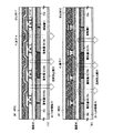
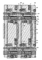
ここで画素部を上面から見た図を図9に示す。また、図9において、A−A’で切断した断面図を図10(A)に、B−B’で切断した断面図を図10(B)に、C−C’で切断した断面図を図10(C)に示す。なお、図10(A)はスイッチングTFT403の断面構造を示し、図10(B)は電流制御TFT404の断面構造を示し、図10(C)は保持容量の断面構造を示している。ここに示す画素部は図5〜図8に示した作製工程により形成可能であり、必要に応じて図5〜図8で用いた符号を参照する。
【0101】
まず、スイッチングTFT403について図9および図10(A)を用いて説明する。図9、図10(A)において、601は活性層である。活性層601の詳細は図7(B)で説明した通りであるからここでの説明は省略する。そして、ソース配線340は配線377を介して活性層601と電気的に接続され、さらに配線378を介してドレイン配線341と電気的に接続される。
【0102】
また、活性層601上にはゲート電極602が設けられている。なお、ゲート電極602のうち、活性層601と重なる部分が図5(E)のゲート電極337、338に相当する。また、ゲート電極602はコンタクト部603にてゲート配線604と電気的に接続される。
【0103】
次に、電流制御TFT404について図9および図10(B)を用いて説明する。図9、図10(B)において、605は活性層である。活性層605の詳細は図7(B)で説明した通りであるからここでの説明は省略する。活性層605のソース領域は配線(電流供給線)379と電気的に接続され、ドレイン領域は配線380および画素電極(EL素子の陽極)381と電気的に接続される。
【0104】
また、活性層605上にはゲート電極339が設けられている。ゲート電極339はドレイン配線341が活性層605と重なる部分に相当する。また、ドレイン配線341はそのまま延長されて図10(C)に示す保持容量の上部電極606を兼ねる。配線(電流供給線)379はコンタクト部607にて半導体膜608と電気的に接続され、この半導体膜608が保持容量の下部電極として機能する。
【0105】
また、本実施例のEL発光装置の回路構成例を図11に示す。なお、本実施例ではデジタル駆動を行うための回路構成を示す。本実施例では、ソース側駆動回路801、画素部808及びゲート側駆動回路809を有している。なお、本明細書中において、駆動回路部とはソース側駆動回路およびゲート側駆動回路を含めた総称である。
【0106】
本実施例では画素部808にスイッチングTFTとして図7(B)に示した構造のnチャネル型TFTが設けられ、このスイッチングTFTはゲート側駆動回路809に接続されたゲート配線とソース側駆動回路801に接続されたソース配線との交点に配置されている。また、スイッチングTFTのドレインはpチャネル型の電流制御TFTのゲートに電気的に接続されている。
【0107】
ソース側駆動回路801は、シフトレジスタ802、バッファ803、ラッチ(A)804、バッファ805、ラッチ(B)806、バッファ807を設けている。なお、アナログ駆動の場合はラッチ(A)、(B)の代わりにサンプリング回路(トランスファゲート)を設ければ良い。また、ゲート側駆動回路809は、シフトレジスタ810、バッファ811を設けている。
【0108】
なお、図示していないが、画素部808を挟んでゲート側駆動回路809の反対側にさらにゲート側駆動回路を設けても良い。この場合、双方は同じ構造でゲート配線を共有しており、片方が壊れても残った方からゲート信号を送って画素部を正常に動作させるような構成とする。
【0109】
なお、上記構成は、図5〜図7に示した作製工程に従ってTFTを作製することによって容易に実現することができる。また、本実施例では画素部と駆動回路部の構成のみ示しているが、本実施例の作製工程に従えば、その他にも信号分割回路、D/Aコンバータ、オペアンプ、γ補正回路などの論理回路を同一基板上に形成することが可能であり、さらにはメモリやマイクロプロセッサ等を形成しうると考えている。
【0110】
さらに、EL素子を保護するための封止(または封入)工程まで行った後の本実施例のEL発光装置について12(A)、(B)を用いて説明する。なお、必要に応じて図11で用いた符号を引用する。
【0111】
図12(A)は、EL素子の封止までを行った状態を示す上面図である。点線で示された801はソース側駆動回路、808は画素部、809はゲート側駆動回路である。また、901はカバー材、902は第1シール材、903は第2シール材であり、第1シール材902で囲まれた内側のカバー材901とEL素子が形成された基板との間には封止材(図示せず)が設けられる。
【0112】
なお、904はソース側駆動回路801及びゲート側駆動回路809に入力される信号を伝達するための接続配線であり、外部入力端子となるFPC905からビデオ信号やクロック信号を受け取る。
【0113】
ここで、図12(A)をA−A’で切断した断面に相当する断面図を図12(B)に示す。なお、図12(A)、(B)では同一の部位に同一の符号を用いている。
【0114】
図12(B)に示すように、ガラス基板906上には画素部808、ゲート側駆動回路809が形成されており、画素部808は電流制御TFT404とそのドレインに電気的に接続された画素電極381を含む複数の画素により形成される。また、ゲート側駆動回路809はpチャネル型TFT401とnチャネル型TFT402とを相補的に組み合わせたCMOS回路を用いて形成される。
【0115】
画素電極381はEL素子の陽極として機能する。また、画素電極381の両端にはバンク382が形成され、画素電極381上にはEL層383およびEL素子の陰極384が形成される。陰極384は全画素に共通の配線としても機能し、接続配線904を経由してFPC905に電気的に接続されている。さらに、画素部808及びゲート側駆動回路809に含まれる素子は全て陰極384で覆われている。
【0116】
また、第1シール材902によりカバー材901が貼り合わされている。このとき、カバー材901とEL素子との間隔を確保するために樹脂膜からなるスペーサを設けても良い。そして、第1シール材902の内側には封止材907が充填されている。なお、第1シール材902、封止材907としては光硬化性樹脂を用いるのが好ましい。また、第1シール材902はできるだけ水分や酸素を透過しない材料であることが望ましい。さらに、封止材907の内部に吸湿効果をもつ物質や酸化防止効果をもつ物質を含有させても良い。
【0117】
EL素子を覆うようにして設けられた封止材907はカバー材901を接着するための接着剤としても機能する。封止材907としては、ポリイミド、アクリル、PVC(ポリビニルクロライド)、エポキシ樹脂、シリコーン樹脂、PVB(ポリビニルブチラル)またはEVA(エチレンビニルアセテート)を用いることができる。
【0118】
また、本実施例ではカバー材901としては、ガラス板、石英板、プラスチック板、セラミックス板、FRP(Fiberglass-Reinforced Plastics)板、PVF(ポリビニルフロライド)フィルム、マイラーフィルム、ポリエステルフィルムまたはアクリルフィルムを用いることができる。
【0119】
さらに本実施例ではカバー材901の両面に炭素膜(具体的にはDLC膜)908a、908bを2〜30nmの厚さに設けている。このような炭素膜は、酸素および水の侵入を防ぐとともにカバー材901の表面を機械的に保護する役割をもつ。勿論、外側の炭素膜908aに偏光板(代表的には円偏光板)を貼り付けることも可能である。
【0120】
また、封止材907を用いてカバー材901を接着した後、封止材907の側面(露呈面)を覆うように第2シール材903を設ける。第2シール材903は第1シール材902と同じ材料を用いることができる。
【0121】
以上のような構造でEL素子を封止材907に封入することにより、EL素子を外部から完全に遮断することができ、外部から水分や酸素等のEL層の酸化による劣化を促す物質が侵入することを防ぐことができる。従って、信頼性の高いEL発光装置を作製することができる。
【0122】
〔実施例5〕
本実施例では、着色層の配置の例について図14を用いて説明する。図14に示すのは、画素部を上面から見た図であり、各画素の構造は図9、図10(A)〜図10(C)を用いて説明したものと同様である。
【0123】
図14において、1101は着色層(R)、1102は着色層(G)、1103は着色層(B)である。また、1104は赤色に発色させる画素、1105は緑色に発色させる画素、1106は青色に発色させる画素である。本実施例では、赤色に発色させる画素1104には着色層(R)1101を設け、緑色に発色させる画素1105には着色層(G)1102を設け、青色に発色させる画素1106には着色層(B)1103を設ける。
【0124】
また、着色層(R)1101、着色層(G)1102および着色層(B)1103は各々ソース配線1107および電流供給線1108の上方で重なり合い、遮光部1109a〜1109dおよび1110を形成している。このように各画素は遮光部1109a〜1109dおよび1110によって囲まれた構造となり、各画素で生成された発光のうち遮光部1109a〜1109dおよび1110に到達した光は吸収される。即ち、隣接する画素間において色混合を効果的に抑制することが可能である。
【0125】
なお、各着色層に黒色顔料やカーボン粒子を含有させておくことは有効である。これにより外部からの光が吸収されるため、画像を観測する人が金属膜からなる陰極に映り込む不具合を低減することができる。但し、含有量が多すぎると発光量自体も低下してしまうので、1〜10%の添加量とすることが望ましい。
【0126】
なお、本実施例は発明の実施の形態で説明したEL発光装置と組み合わせても良いし、実施例1〜実施例4のいずれの構成とも自由に組み合わせて実施することが可能である。
【0127】
〔実施例6〕
発明の実施の形態および実施例4ではEL層に含まれた発光層として白色発光が得られるEL材料を用い、そこから放射された白色光を、着色層(R)、着色層(G)もしくは着色層(B)に通すことにより赤色光、緑色光もしくは青色光を得る例を示した。
【0128】
本実施例では、赤色に発色させる画素には赤色発光が得られる発光層を形成し、緑色に発色させる画素には緑色発光が得られる発光層を形成し、青色に発色させる画素には青色発光が得られる発光層を形成する。そして、各発光層から放射された赤色光、緑色光もしくは青色光を、それぞれ着色層(R)、着色層(G)もしくは着色層(B)に通すことで色純度を向上させる。
【0129】
本実施例の場合、赤色、緑色もしくは青色の発光が得られる三種類のEL材料を成膜する必要があるが、公知の材料を用いることができる。また、画素ごとに分けて成膜する必要があるため、シャドーマスクを用いた蒸着法により低分子系EL材料を成膜するか、インクジェット法や印刷法により高分子系EL材料を成膜すれば良い。
【0130】
なお、本実施例の構成は発明の実施の形態、実施例1〜実施例5のいずれの構成とも自由に組み合わせて実施することが可能である。また、実施例5に示したように各着色層に黒色顔料やカーボン粒子を含有させておくことは有効である。
【0131】
〔実施例7〕
本実施例では、発光層として青色もしくは青緑色の発光が得られるEL材料を用い、その発光を色変換層に通すことにより赤色光、緑色光もしくは青色光を得る例を示す。
【0132】
本実施例の場合、赤色に発色させる画素には青色光を赤色光に変換する色変換層を形成し、緑色に発色させる画素には青色光を緑色光に変換する色変換層を形成する。この色変換層は公知のものを用いれば良い。発光層から放射された青色光は色変換層を励起して赤色光もしくは緑色光を生成する。
【0133】
そして、各色変換層から放射された赤色光、緑色光および発光層から放射された青色光を、それぞれ着色層(R)、着色層(G)もしくは着色層(B)に通すことで色純度を向上させる。
【0134】
本実施例では、発光層として青色もしくは青緑色の発光が得られる発光層だけを成膜すれば良いため、スピンコート法や印刷法のように簡便な技術で成膜することが好ましい。勿論、蒸着法で成膜することも可能である。
【0135】
なお、本実施例の構成は発明の実施の形態、実施例1〜実施例5のいずれの構成とも自由に組み合わせて実施することが可能である。また、実施例5に示したように各着色層に黒色顔料やカーボン粒子を含有させておくことは有効である。
【0136】
〔実施例8〕
本実施例では実施例4と異なる構造の画素部を有したEL発光装置を示す。なお、各種配線(ゲート配線、ソース配線、ドレイン配線もしくは電流供給線等)の形成される層が異なる以外、TFT構造およびEL素子構造は実施例4とほぼ同様である。従って、実施例4と同じ部分に関しては、図9、図10(A)〜図10(C)で用いた符号を引用することにする。
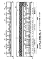
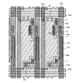
【0137】
ここで画素部を上面から見た図を図15に示す。また、図15において、A−A’で切断した断面図を図16(A)に、B−B’で切断した断面図を図16(B)に、C−C’で切断した断面図を図16(C)に示す。なお、図16(A)はスイッチングTFTの断面構造を示し、図16(B)は電流制御TFTの断面構造を示し、図16(C)は保持容量の断面構造を示している。また、ここに示す画素部は図5〜図7に示した作製工程を参照すれば形成できる。
【0138】
まず、スイッチングTFTについて図15および図16(A)を用いて説明する。図15、図16(A)において、1201は活性層である。活性層1201の詳細は図7(B)で説明したスイッチングTFTと同様であるからここでの説明は省略する。活性層1201の上にはゲート配線1202が重なりゲート電極として機能している。そして、活性層1201にはソース配線1203およびドレイン配線1204が接続され、ドレイン配線1203は電流制御TFTのゲート配線1205に接続される。
【0139】
次に、電流制御TFTについて図15および図16(B)を用いて説明する。なお、電流制御TFTは二つのTFTが並列に接続された構造となっているが、ここではその片方についての説明を行う。図15、図16(B)において、1206は活性層である。活性層1206の詳細は図7(B)で説明した電流制御TFTと同様であるからここでの説明は省略する。活性層1206のソース領域は電流供給線1207に接続され、ドレイン領域はドレイン配線1208を介して画素電極(EL素子の陽極)1209と電気的に接続される。
【0140】
また、電流制御TFTのゲート配線1205は電流供給線1207の直下において図16(C)に示す保持容量1210の上部電極1211を兼ねる。このとき、電流供給線1207は半導体膜1212と電気的に接続され、この半導体膜1212が保持容量1210の下部電極として機能する。本実施例の構造にすると保持容量1210が完全に電流供給線1207の下に隠れるため、画素の有効発光面積を狭くするようなことがない。
【0141】
次に、消去TFTについて説明する。本実施例の画素にはスイッチングTFTと同じ構造の消去TFT1213が設けられている。消去TFT1213の活性層1214は、ソース領域が電流供給線1207に接続され、ドレイン領域がドレイン配線1215を介して電流制御TFTのゲート配線1205と電気的に接続される。なお、活性層1214の構造はスイッチングTFTと同様であるからここでの説明は省略する。
【0142】
また、消去TFTのゲート配線(以下、消去ゲート配線という)1216はスイッチングTFTのゲート配線1202と平行に設けられている。
【0143】
消去ゲート配線1216に消去TFT1213をオン状態にする信号が入ると電流制御TFTのゲート配線1205は強制的に電流供給線1207と同電位になる。即ち、電流制御TFTがオフ状態になるためEL素子385への電流の供給がなくなり、発光が止まって画素は消灯する。
【0144】
このように、消去TFT1213を設けることで画素を強制的に消灯することができ、画素の点灯時間の制御性が高まる。即ち、時間階調方式の画像表示において、階調数を容易に上げることが可能となる。なお、このような消去TFTを用いたEL発光装置に関して特願平11−338786号を引用すれば良い。
【0145】
また、本実施例の構成は発明の実施の形態、実施例2、実施例3もしくは実施例5〜実施例7のいずれの構成とも自由に組み合わせて実施することが可能である。
【0146】
〔実施例9〕
本実施例では実施例4と異なる作製工程でEL発光装置を作製する例について図17を用いて説明する。なお、実施例4と途中の工程が異なるだけであるので必要に応じて実施例4で用いた符号を参照する。
【0147】
まず、実施例4の作製工程に従って、図5(E)の工程まで行う。但し、本実施例では図5(C)に示したn型不純物元素の添加工程を省略する。こうして図17(A)の状態が得られる。
【0148】
次に、図17(B)に示すように、レジストマスク311a〜311eを除去した後、半導体膜にn型不純物元素(本実施例ではリン)を添加する。なお、ここで行うn型不純物元素の添加工程は、実施例1の図6(A)に示した添加工程と同様の条件で行えば良い。
【0149】
こうして、n型不純物領域(b)501〜509およびn型不純物領域(c)510〜519が形成される。なお、n型不純物領域(b)501〜509およびn型不純物領域(c)510〜519に含まれるn型不純物元素の濃度は実施例4を参照すれば良い。
【0150】
次に、レジストマスク520a〜520eを形成し、実施例1の図5(C)に示した添加工程と同様にn型不純物元素(本実施例ではリン)を添加する。こうしてn型不純物領域(a)521〜529が形成される。なお、n型不純物領域(a)521〜529に含まれるn型不純物元素の濃度は実施例4を参照すれば良い。(図17(C))
【0151】
このとき、n型不純物領域(b)501〜509のうちレジストマスク520a〜520eで隠された部分は、後にLDD(ライトドープドレイン)領域として機能する。本実施例は後にLDD領域として機能するn型不純物領域(b)の長さ(LDD長さ)をレジストマスク520a〜520eで自由に調節できるためLDD長さの制御性に優れる点に特徴がある。
【0152】
次に、レジストマスク520a〜520eを除去し、レジストマスク530を形成する。そして、実施例4の図6(B)に示した添加工程と同様にp型不純物元素(本実施例ではボロン)を添加する。こうしてp型不純物領域(a)531〜534が形成される。なお、p型不純物領域(a)531〜534に含まれるp型不純物元素の濃度は実施例4を参照すれば良い。(図17(D))
【0153】
このあとは、実施例4の図6(C)に示した活性化工程以降の工程に従ってEL発光装置を作製すれば良い。また、完成したTFT構造は実施例4とほぼ同様であるため、実施例4の説明を参照すれば良い。なお、本実施例は発明の実施の形態、実施例2〜実施例8のいずれの構成とも自由に組み合わせて実施することが可能である。
【0154】
〔実施例10〕
本実施例では実施例4と異なる作製工程でEL発光装置を作製する例について図18を用いて説明する。なお、実施例4と途中の工程が異なるだけであるので必要に応じて実施例4で用いた符号を参照する。
【0155】
まず、実施例4の作製工程に従って、図5(E)の工程まで行う。但し、本実施例では図5(C)に示したn型不純物元素の添加工程を省略する。こうして図18(A)の状態が得られる。
【0156】
次に、図18(B)に示すように、レジストマスク311a〜311eを除去した後、n型不純物元素(本実施例ではリン)を添加する。なお、ここで行うn型不純物元素の添加工程は、実施例4の図6(A)に示した添加工程と同様の条件で行えば良い。
【0157】
こうして、n型不純物領域(b)501〜509およびn型不純物領域(c)510〜519が形成される。なお、n型不純物領域(b)501〜509およびn型不純物領域(c)510〜519に含まれるn型不純物元素の濃度は実施例4を参照すれば良い。
【0158】
次に、ゲート電極335〜339をマスクとして、半導体膜に実施例4の図5(C)に示した添加工程と同様にn型不純物元素(本実施例ではリン)を添加する。こうしてn型不純物領域(a)541〜549が形成される。なお、n型不純物領域(a)541〜549に含まれるn型不純物元素の濃度は実施例4を参照すれば良い。(図18(C))
【0159】
次に、レジストマスク550を形成し、実施例4の図6(B)に示した添加工程と同様にp型不純物元素(本実施例ではボロン)を添加する。こうしてp型不純物領域(a)551〜554が形成される。なお、p型不純物領域(a)551〜554に含まれるp型不純物元素の濃度は実施例4を参照すれば良い。(図18(D))
【0160】
このあとは、実施例4の図6(C)に示した活性化工程以降の工程に従ってEL発光装置を作製すれば良い。また、完成したTFT構造は実施例4とほぼ同様であるため、実施例4の説明を参照すれば良い。なお、本実施例は発明の実施の形態、実施例2〜実施例8のいずれの構成とも自由に組み合わせて実施することが可能である。
【0161】
〔実施例11〕
実施例4では層間絶縁膜373として樹脂膜を用いたが、本実施例では珪素を含む絶縁膜、具体的には酸化珪素膜を用いる。本実施例の場合、まず図6(B)の工程まで終えたら、ゲート電極を覆うように100〜200nmの厚さの保護膜(本実施例では窒化酸化珪素膜)を形成する。
【0162】
次に、図6(C)と同様に活性化工程を行い、次に800nm〜1μmの厚さの層間絶縁膜(本実施例では酸化珪素膜)を設ける。本実施例では、この層間絶縁膜を形成する前に3〜100%の水素を含む雰囲気中にて350〜500℃の熱処理を行い、活性層の不対結合手を励起された水素で終端する。
【0163】
これらの工程の後、ソース配線もしくはドレイン配線を前記層間絶縁膜上に形成し、ソース配線およびドレイン配線をパッシベーション膜で覆う。本実施例ではパッシベーション膜として窒化珪素膜もしくは窒化酸化珪素膜を用いる。
【0164】
なお、本実施例の構成は発明の実施の形態、実施例2〜実施例10のいずれの構成とも自由に組み合わせて実施することが可能である。
【0165】
〔実施例12〕
本実施例では、実施例4に示したEL表示装置とは異なる構造でEL素子を封止した例について図13を用いて説明する。なお、図12と同一の部分については同一の符号を用いる。
【0166】
本実施例ではカバー材1001として、両面にDLC膜1002aおよび1002bを形成したプラスチックフィルムを用いる。プラスチックフィルムの両面にDLC膜を形成する場合、プラスチックフィルムをロールに巻いて成膜を行うロールトゥロール方式を用いれば良い。
【0167】
本実施例では、実施例4に従ってEL素子まで作製した基板に、封止材1003を用いてカバー材1001を貼り合わせる。そして、カバー材1001の端部はシール材1004で封止する。本実施例で用いる封止材1003およびシール材1004に関しては、実施例4に示した材料を用いることができる。
【0168】
なお、本実施例の構成は発明の実施の形態、実施例1〜11のいずれの構成とも自由に組み合わせて実施することが可能である。
【0169】
〔実施例13〕
本実施例では、実施例4において図9に示した画素構造および実施例8において図15に示した画素構造の回路図について説明する。ここでは図9に対応した回路図を図19(A)に、図15に対応した回路図を図19(B)に示す。
【0170】
図19(A)において、340はソース配線、379は電流供給線、604はゲート配線である。これらの符号は図9に対応している。また、1601は図10(A)に示したスイッチングTFT、1602は図10(B)に示した電流制御TFT、1603は図10(C)に示した保持容量、1604はEL素子である。
【0171】
本実施例に示した画素をデジタル駆動する場合には、特願2000−114592号に記載の駆動方法を引用すれば良い。
【0172】
次に、図19(B)において、1203はソース配線、1207は電流供給線、1202はゲート配線である。これらの符号は図15に対応している。また、1605は図16(A)に示したスイッチングTFT、1606は図16(B)に示した電流制御TFT、1607は図16(C)に示した保持容量、1608はEL素子、1609は消去TFTである。
【0173】
本実施例に示した画素をデジタル駆動する場合には、特願平11−338786号に記載の駆動方法を引用すれば良い。
【0174】
なお、本実施例の構成は発明の実施の形態、実施例2〜12のいずれの構成とも自由に組み合わせて実施することが可能である。
【0175】
〔実施例14〕
本実施例ではアクティブマトリクス基板が完成した後で基板を剥離してカラーフィルタを貼り合わせる場合の例について説明する。なお、本実施例の工程は実施例3の構造を実現する上で有効である。
【0176】
まず、実施例4の作製工程に従って、図7(B)に示す構造のアクティブマトリクス基板を完成する。但し、本実施例では基板301と下地膜302の間に剥離層1701が設けられている。本実施例では剥離層1701として非晶質珪素膜(多結晶珪素膜でも良い)を用いる。また、カバー材388としては、プラスチックフィルム1702を用い、プラスチックフィルム1702の両面にはDLC膜1703aおよび1703bが設けられている。(図20(A))
【0177】
次に、アクティブマトリクス基板全体を、フッ化ハロゲンを含むガス中に晒し、剥離層1701の除去を行う。本実施例ではフッ化ハロゲンとして三フッ化塩素(ClF3)を用い、希釈ガスとして窒素を用いる。希釈ガスとしては、アルゴン、ヘリウムもしくはネオンを用いても良い。流量は共に500sccm(8.35×10⁻⁶m3/s)とし、反応圧力は1〜10Torr(1.3×102〜1.3×103Pa)とすれば良い。また、処理温度は室温(典型的には20〜27℃)で良い。
【0178】
なお、フッ化ハロゲンとは化学式XFn(Xはフッ素以外のハロゲン、nは整数)で示される物質であり、一フッ化塩素(ClF)、三フッ化塩素(ClF3)、一フッ化臭素(BrF)、三フッ化臭素(BrF3)、一フッ化ヨウ素(IF)もしくは三フッ化ヨウ素(IF3)を用いることができる。フッ化ハロゲンは、珪素膜と酸化珪素膜とのエッチング時の選択比が大きく、珪素膜の選択的なエッチングが可能である。
【0179】
この場合、剥離層である珪素膜はエッチングされるが、ガスに晒される他の部分(炭素膜、プラスチックフィルム、ガラス基板、樹脂膜および酸化珪素膜が露呈した部分)はエッチングされない。即ち、三フッ化塩素ガスに晒すことで剥離層1701が選択的にエッチングされ、最終的には完全に除去される。
【0180】
本実施例の場合、剥離層1701は露呈した端部から徐々にエッチングされていき、完全に除去された時点で基板301と下地膜302が分離される。このとき、TFT及びEL素子は薄膜を積層して形成されているが、プラスチックフィルム1702に移された形で残る。(図20(B))
【0181】
この剥離技術は本出願人による特願2000−008403号に記載された技術を引用すれば良い。また、特願2000−071673号に記載された技術を引用することもできる。
【0182】
次に、図21に示すように、プラスチックフィルム1704の両面にDLC膜1705a、1705bを設け、その上に着色層(R)391aおよび着色層(B)391bを形成し、樹脂層393を形成してカラーフィルタを作製する。そして、そのカラーフィルタを下地膜302に貼り合わせる。
【0183】
本実施例の場合、TFTおよびEL素子がプラスチックフィルムに挟まれた状態となっているため、発光装置全体が可撓性になる。また、全ての基板がプラスチックフィルムで形成されているため、薄型で軽量なEL発光装置が得られる。
【0184】
〔実施例15〕
本発明を実施するにあたってEL素子を形成するために用いる成膜装置の例を図22に示す。なお、本実施例ではインライン方式の成膜装置とした場合について説明する。図22において201はロード室であり、基板40の搬送はここから行われる。ロード室201には排気系200aが備えられ、排気系200aは第1バルブ41、ターボ分子ポンプ42、第2バルブ43及びロータリーポンプ(油回転ポンプ)44を含んだ構成からなっている。
【0185】
第1バルブ41はメインバルブであり、コンダクタンスバルブを兼ねる場合もあるしバタフライバルブを用いる場合もある。第2バルブ43はフォアバルブであり、まず第2バルブ43を開けてロータリーポンプ44によりロード室201を粗く減圧し、次に第1バルブ41を空けてターボ分子ポンプ42で高真空まで減圧する。なお、ターボ分子ポンプの代わりにメカニカルブースターポンプ若しくはクライオポンプを用いることが可能であるがクライオポンプは水分の除去に特に効果的である。
【0186】
次に、202で示されるのはEL素子の陽極もしくは陰極(本実施例では陽極)の表面を処理する前処理室であり、前処理室202は排気系200bを備えている。また、ロード室201とは図示しないゲートで密閉遮断されている。前処理室202はEL素子の作製プロセスによって様々に変えることができる。
【0187】
前処理としては、オゾンプラズマ処理、酸素プラズマ処理、アルゴンプラズマ処理、ネオンプラズマ処理、ヘリウムプラズマ処理もしくは水素プラズマ処理を行うことができる。また、ヒーターを備えることでプラズマ処理と同時に加熱することも可能である。さらに、紫外光ランプを備えることで紫外光照射を可能とすることも有効である。
【0188】
本実施例では、基板を100℃に加熱しながら酸化物導電膜からなる陽極の表面にオゾンプラズマ処理を行い、水分の除去と同時に陽極表面の仕事関数を高める前処理を行う。
【0189】
次に、203は蒸着法により有機材料を成膜するための蒸着室であり、蒸着室(A)と呼ぶ。蒸着室(A)203は排気系200cを備えている。また、前処理室202とは図示しないゲートで密閉遮断されている。本実施例では蒸着室(A)203にて正孔注入層を形成する。
【0190】
次に、204は蒸着法により有機材料を成膜するための蒸着室であり、蒸着室(B)と呼ぶ。蒸着室(B)204は排気系200dを備えている。また、蒸着室(A)203とは図示しないゲートで密閉遮断されている。本実施例では蒸着室(B)204にて正孔輸送層を形成する。
【0191】
次に、205は蒸着法により有機EL材料を成膜するための蒸着室であり、蒸着室(C)と呼ぶ。蒸着室(C)205は排気系200eを備えている。また、蒸着室(B)204とは図示しないゲートで密閉遮断されている。本実施例では、蒸着室(C)205において、赤色に発色する発光層を形成する。
【0192】
次に、206は蒸着法により有機EL材料を成膜するための蒸着室であり、蒸着室(D)と呼ぶ。蒸着室(D)206は排気系200fを備えている。また、蒸着室(C)205とは図示しないゲートで密閉遮断されている。本実施例では、蒸着室(D)206において、緑色に発色する発光層を形成する。
【0193】
次に、207は蒸着法により有機EL材料を成膜するための蒸着室であり、蒸着室(E)と呼ぶ。蒸着室(E)207は排気系200gを備えている。また、蒸着室(D)206とは図示しないゲートで密閉遮断されている。本実施例では、蒸着室(E)207において、青色に発色する発光層を形成する。
【0194】
次に、208は蒸着法により有機材料を成膜するための蒸着室であり、蒸着室(F)と呼ぶ。蒸着室(F)208は排気系200hを備えている。また、蒸着室(E)207とは図示しないゲートで密閉遮断されている。本実施例では蒸着室(F)208にて電子輸送層を形成する。
【0195】
次に、209は蒸着法により有機材料を成膜するための蒸着室であり、蒸着室(G)と呼ぶ。蒸着室(G)209は排気系200iを備えている。また、蒸着室(F)208とは図示しないゲートで密閉遮断されている。本実施例では蒸着室(G)209にて電子注入層を形成する。
【0196】
次に、210は蒸着法によりEL素子の陽極もしくは陰極となる導電膜(本実施例では陰極となる金属膜)を成膜するための蒸着室であり、蒸着室(H)と呼ぶ。蒸着室(H)210は排気系200jを備えている。また、蒸着室(G)209とは図示しないゲートで密閉遮断されている。
【0197】
本実施例では、蒸着室(H)210にて、EL素子の陰極となる導電膜としてAl−Li合金膜(アルミニウムとリチウムとの合金膜)もしくはAl−Cs合金膜(アルミニウムとセシウムとの合金膜)を形成する。なお、周期表の1族もしくは2族に属する元素とアルミニウムとを共蒸着することも可能である。
【0198】
次に、211は封止室であり、排気系200kを備えている。また、蒸着室(H)210とは図示しないゲートで密閉遮断されている。封止室211ではEL素子を酸素および水分から保護するために、パッシベーション膜としてDLC(ダイヤモンドライクカーボン)膜を形成する。
【0199】
DLC膜を形成するにはスパッタ法もしくはプラズマCVD法を用いれば良い。DLC膜は室温から100℃以下の温度範囲で成膜できるため、耐熱性の低いEL素子を保護するパッシベーション膜として好適である。また、熱伝導率が高く放熱効果が良いため、EL素子の熱劣化を抑制する効果も期待できる。なお、本実施例で形成するDLC膜は窒化珪素膜もしくは炭化珪素膜と積層して用いることも有効である。
【0200】
さらに、DLC膜中にフッ素や水素を添加しても良い。また、DLC膜中の酸素濃度を1×10¹⁸atoms/cm3以下とすることで酸素の透過率を低減することが可能である。
【0201】
最後に、212はアンロード室であり、排気系200lを備えている。EL素子が形成された基板はここから取り出される。
【0202】
以上のように、図22に示した成膜装置を用いることで完全にEL素子を密閉空間に封入するまで外気に晒さずに済むため、信頼性の高いEL表示装置を作製することが可能となる。また、インライン方式により高いスループットでEL表示装置を作製することができる。
【0203】
さらに、本実施例に示した成膜装置の各処理室、排気系および搬送系をコンピュータ制御により動作させることは有効である。本実施例の場合、連続的に一連の処理を行ってEL素子が完成するため、コンピュータ制御により基板投入から基板取り出しまでを管理することができる。
【0204】
なお、本実施例に示した成膜装置を用いて発明の実施の形態、実施例1〜14に示したいずれの構成のEL表示装置を作製しても良い。
【0205】
〔実施例16〕
本発明において、三重項励起子からの燐光を発光に利用できるEL材料を用いることで、外部発光量子効率を飛躍的に向上させることができる。これにより、EL素子の低消費電力化、長寿命化、および軽量化が可能になる。
ここで、三重項励起子を利用し、外部発光量子効率を向上させた報告を示す。
(T.Tsutsui, C.Adachi, S.Saito, Photochemical Processes in Organized Molecular Systems, ed.K.Honda, (Elsevier Sci.Pub., Tokyo,1991) p.437.)
上記論文に報告されたEL材料(クマリン色素)の分子式を以下に示す。
【0206】
【化1】

(M.A.Baldo, D.F.O'Brien, Y.You, A.Shoustikov, S.Sibley, M.E.Thompson, S.R.Forrest, Nature 395 (1998) p.151.)
上記論文に報告されたEL材料(Pt錯体)の分子式を以下に示す。
【0208】
【化2】
(M.A.Baldo, S.Lamansky, P.E.Burrrows, M.E.Thompson, S.R.Forrest, Appl.Phys.Lett.,75 (1999) p.4.)
(T.Tsutsui, M.-J.Yang, M.Yahiro, K.Nakamura, T.Watanabe, T.tsuji, Y.Fukuda, T.Wakimoto, S.Mayaguchi, Jpn.Appl.Phys., 38 (12B) (1999) L1502.)
上記論文に報告されたEL材料(Ir錯体)の分子式を以下に示す。
【0210】
【化3】
以上のように三重項励起子からの燐光発光を利用できれば原理的には一重項励起子からの蛍光発光を用いる場合より3〜4倍の高い外部発光量子効率の実現が可能となる。なお、本実施例の構成は、発明の実施の形態、実施例1〜実施例15のいずれの構成とも自由に組み合わせて実施することが可能である。
【0212】
〔実施例17〕
本実施例では、実施例4において図7(B)に示したEL素子385の具体的な例について図23を用いて説明する。なお、本実施例に示すEL素子の構造例は図7(B)のEL素子385の部分を拡大した例に相当する。また、本実施例のEL素子を図22に示した装置で作製した例を示す。
【0213】
なお、本実施例でEL層を形成する材料は公知の有機材料もしくは無機材料を用いることができる。また、高分子系材料であっても低分子系材料であっても良い。
【0214】
まず、図23(A)は、陽極(画素電極)51上に正孔注入層52、正孔輸送層53、発光層54、電子輸送層55、電子注入層56および陰極57を積層した構造のEL素子である。なお、発光層54は赤、緑、青に対応した三種類の発光層を成膜しても良い。
【0215】
本実施例では、前処理室202で陽極51の表面改善を行い、蒸着室(A)203で正孔注入層52を形成し、蒸着室(B)204で正孔輸送層53を形成し、蒸着室(C)205〜蒸着室(E)207で発光層54を形成し、蒸着室(F)208で電子輸送層55を形成し、蒸着室(G)209で電子注入層56を形成し、蒸着室(H)210で陰極57を形成する。
【0216】
次に、図23(B)は、陽極(画素電極)51上に正孔注入層52、正孔輸送層53、発光層54、電子注入層56および陰極57を積層した構造のEL素子である。なお、発光層54は赤、緑、青に対応した三種類の発光層を成膜しても良い。
【0217】
本実施例では、前処理室202で陽極51の表面改善を行い、蒸着室(A)203で正孔注入層52を形成し、蒸着室(B)204で正孔輸送層53を形成し、蒸着室(C)205〜蒸着室(E)207で発光層54を形成し、蒸着室(F)208を通過させて、蒸着室(G)209で電子注入層56を形成し、蒸着室(H)210で陰極57を形成する。
【0218】
次に、図23(C)は、陽極(画素電極)51上に正孔注入層52、発光層54、電子輸送層55、電子注入層56および陰極57を積層した構造のEL素子である。なお、発光層54は赤、緑、青に対応した三種類の発光層を成膜しても良い。
【0219】
本実施例では、前処理室202で陽極51の表面改善を行い、蒸着室(A)203で正孔注入層52を形成し、蒸着室(B)204を通過させて、蒸着室(C)205〜蒸着室(E)207で発光層54を形成し、蒸着室(F)208で電子輸送層55を形成し、蒸着室(G)209で電子注入層56を形成し、蒸着室(H)210で陰極57を形成する。
【0220】
次に、図23(D)は、陽極(画素電極)51上に正孔注入層52、発光層54、電子注入層56および陰極57を積層した構造のEL素子である。なお、発光層54は赤、緑、青に対応した三種類の発光層を成膜しても良い。
【0221】
本実施例では、前処理室202で陽極51の表面改善を行い、蒸着室(A)203で正孔注入層52を形成し、蒸着室(B)204を通過させて、蒸着室(C)205〜蒸着室(E)207で発光層54を形成し、蒸着室(F)208を通過させて、蒸着室(G)209で電子注入層56を形成し、蒸着室(H)210で陰極57を形成する。
【0222】
次に、図23(E)は、陽極(画素電極)51上にクラスター58、正孔注入層52、発光層54、電子輸送層55、電子注入層56および陰極57を積層した構造のEL素子である。なお、発光層54は赤、緑、青に対応した三種類の発光層を成膜しても良い。また、クラスター58は陽極51の仕事関数を高めるために設けられ、本実施例ではイリジウム、ニッケルもしくは白金をクラスター状(塊状)に設ける。このクラスター18は直径もしくは長径が10〜100nm、高さ5〜50nmとすることが好ましい。
【0223】
本実施例では、前処理室202で陽極51の表面改善を行い、蒸着室(A)でクラスター58を形成し、蒸着室(B)204で正孔注入層52を形成し、蒸着室(C)205〜蒸着室(E)207で発光層54を形成し、蒸着室(F)208で電子輸送層55を形成し、蒸着室(G)209で電子注入層56を形成し、蒸着室(H)210で陰極57を形成する。
【0224】
次に、図23(F)は、陽極(画素電極)51上にクラスター58、正孔注入層52、発光層54、電子注入層56および陰極57を積層した構造のEL素子である。なお、発光層54は赤、緑、青に対応した三種類の発光層を成膜しても良い。
【0225】
本実施例では、前処理室202で陽極51の表面改善を行い、蒸着室(A)でクラスター58を形成し、蒸着室(B)204で正孔注入層52を形成し、蒸着室(C)205〜蒸着室(E)207で発光層54を形成し、蒸着室(F)208を通過させて、蒸着室(G)209で電子注入層56を形成し、蒸着室(H)210で陰極57を形成する。
【0226】
以上のように、様々な構造のEL素子を形成する場合においても、図22に示したような成膜装置を用いれば容易に作製することが可能である。なお、本実施例に示した構成は発明の実施の形態、実施例1〜実施例15のいずれの構成とも自由に組み合わせて実施することが可能である。
【0227】
〔実施例18〕
本発明を実施して形成された発光装置は、自発光型であるため液晶表示装置に比べて明るい場所での視認性に優れ、しかも視野角が広い。従って、様々な電気器具の表示部として用いることができる。
【0228】
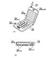
本発明の電気器具としては、ビデオカメラ、デジタルカメラ、ゴーグル型ディスプレイ(ヘッドマウントディスプレイ)、カーナビゲーションシステム、カーオーディオ、ノート型パーソナルコンピュータ、ゲーム機器、携帯情報端末(モバイルコンピュータ、携帯電話、携帯型ゲーム機または電子書籍)、記録媒体を備えた画像再生装置(具体的にはコンパクトディスク(CD)、レーザーディスク(LD)又はデジタルバーサタイルディスク(DVD)等の記録媒体を再生し、その画像を表示しうるディスプレイを備えた装置)などが挙げられる。それら電気器具の具体例を図24、図25に示す。
【0229】
図24(A)はELディスプレイであり、筐体2001、支持台2002、表示部2003を含む。本発明の発光装置は表示部2003に用いることができる。ELディスプレイは自発光型であるためバックライトが必要なく、液晶ディスプレイよりも薄い表示部とすることができる。
【0230】
図24(B)はビデオカメラであり、本体2101、表示部2102、音声入力部2103、操作スイッチ2104、バッテリー2105、受像部2106を含む。本発明の発光装置は表示部2102に用いることができる。
【0231】
図24(C)はデジタルカメラであり、本体2201、表示部2202、接眼部2203、操作スイッチ2204を含む。本発明の発光装置は表示部2202に用いることができる。
【0232】
図24(D)は記録媒体を備えた画像再生装置(具体的にはDVD再生装置)であり、本体2301、記録媒体(CD、LDまたはDVD等)2302、操作スイッチ2303、表示部(a)2304、表示部(b)2305を含む。表示部(a)は主として画像情報を表示し、表示部(b)は主として文字情報を表示するが、本発明の発光装置はこれら表示部(a)、(b)に用いることができる。なお、記録媒体を備えた画像再生装置には、CD再生装置、ゲーム機器なども含まれうる。
【0233】
図24(E)は携帯型(モバイル)コンピュータであり、本体2401、表示部2402、受像部2403、操作スイッチ2404、メモリスロット2405を含む。本発明の電気光学装置は表示部2402に用いることができる。この携帯型コンピュータはフラッシュメモリや不揮発性メモリを集積化した記録媒体に情報を記録したり、それを再生したりすることができる。
【0234】
図24(F)はパーソナルコンピュータであり、本体2501、筐体2502、表示部2503、キーボード2504を含む。本発明の発光装置は表示部2503に用いることができる。
【0235】
なお、将来的にEL材料の発光輝度が高くなれば、出力した画像情報を含む光をレンズ等で拡大投影してフロント型若しくはリア型のプロジェクターに用いることも可能となる。
【0236】
また、上記電子装置はインターネットやCATV(ケーブルテレビ)などの電子通信回線を通じて配信された情報を表示することが多くなり、特に動画情報を表示する機会が増してきている。EL材料の応答速度は非常に高いため、そのような動画表示を行うに適している。
【0237】
また、発光装置は発光している部分が電力を消費するため、発光部分が極力少なくなるように情報を表示することが望ましい。従って、携帯情報端末、特に携帯電話やカーオーディオのような文字情報を主とする表示部に発光装置を用いる場合には、非発光部分を背景として文字情報を発光部分で形成するように駆動することが望ましい。
【0238】
ここで図25(A)は携帯電話であり、本体2601、音声出力部2602、音声入力部2603、表示部2604、操作スイッチ2605、アンテナ2606を含む。本発明の発光装置は表示部2604に用いることができる。なお、表示部2604は黒色の背景に白色の文字を表示することで携帯電話の消費電力を抑えることができる。
【0239】
また、図25(B)はカーオーディオ(車載用オーディオ)であり、本体2701、表示部2702、操作スイッチ2703、2704を含む。本発明の発光装置は表示部2702に用いることができる。また、本実施例では車載用オーディオを示すが、据え置き型(家庭用)オーディオに用いても良い。なお、表示部2704は黒色の背景に白色の文字を表示することで消費電力を抑えられる。
【0240】
さらに、光センサを内蔵させ、使用環境の明るさを検知する手段を設けることで使用環境の明るさに応じて発光輝度を変調させるような機能を持たせることは有効である。使用者は使用環境の明るさに比べてコントラスト比で100〜150の明るさを確保できれば問題なく画像もしくは文字情報を認識できる。即ち、使用環境が明るい場合は画像の輝度を上げて見やすくし、使用環境が暗い場合は画像の輝度を抑えて消費電力を抑えるといったことが可能である。
【0241】
以上の様に、本発明の適用範囲は極めて広く、あらゆる分野の電気器具に用いることが可能である。また、本実施例の電気器具は発明の実施の形態、実施例1〜実施例17の構成を自由に組み合わせたEL発光装置を用いることで得ることができる。
【0242】
【発明の効果】
本発明を実施することでアクティブマトリクス基板もしくはパッシブマトリクス基板とカラーフィルタとを別々の製造工程にて作製するため、発光装置全体としての歩留まりを向上させることができ、さらに、発光装置の製造期間の短縮を図ることができる。その結果、製造コストが低減されることにより安価な発光装置を提供することができる。さらに、安価な発光装置を用いることで安価な電気器具を提供することが可能となる。
【図面の簡単な説明】
【図1】 画素部の断面構造を示す図。
【図2】 画素部の断面構造を示す図。
【図3】 画素部の断面構造を示す図。
【図4】 画素部の断面構造を示す図。
【図5】 画素部および駆動回路の作製工程を示す図。
【図6】 画素部および駆動回路の作製工程を示す図。
【図7】 画素部および駆動回路の作製工程を示す図。
【図8】 画素部および駆動回路の作製工程を示す図。
【図9】 画素部の上面構造を示す図。
【図10】 画素部の断面構造を示す図。
【図11】 EL発光装置の回路構成を示す図。
【図12】 EL発光装置の上面構造および断面構造を示す図。
【図13】 EL発光装置の上面構造および断面構造を示す図。
【図14】 画素部の上面構造を示す図。
【図15】 画素部の上面構造を示す図。
【図16】 画素部の断面構造を示す図。
【図17】 画素部および駆動回路の作製工程を示す図。
【図18】 画素部および駆動回路の作製工程を示す図。
【図19】 画素の回路構成を示す図。
【図20】 画素部の作製工程を示す図。
【図21】 画素部の断面構造を示す図。
【図22】 インライン方式の成膜装置の構成を示す図。
【図23】 EL素子の構造を示す図。
【図24】 電気器具の具体例を示す図。
【図25】 電気器具の具体例を示す図。[0001]
BACKGROUND OF THE INVENTION
The present invention relates to a light emitting device having an element in which a luminescent material is sandwiched between electrodes and an electric appliance using the light emitting device for a display unit (display display or display monitor). In particular, the present invention relates to a light-emitting device using a light-emitting material (hereinafter referred to as EL material) from which EL (Electro Luminescence) can be obtained. An organic EL display and an organic light emitting diode (OLED) are included in the light emitting device of the present invention.
[0002]
The luminescent material that can be used in the present invention includes all luminescent materials that emit light (phosphorescence and / or fluorescence) via singlet excitation, triplet excitation, or both excitation.
[0003]
[Prior art]
In recent years, development of a light-emitting device (hereinafter referred to as an EL light-emitting device) using a light-emitting element (hereinafter referred to as an EL element) using the EL phenomenon of a light-emitting material has been advanced. Since EL light-emitting devices are display devices that use self-luminous elements, they do not require a backlight like a liquid crystal display and have a wide viewing angle, so they are attracting attention as display units for portable devices used outdoors. .
[0004]
There is a method of using a color filter as a method of displaying a color image in an EL light emitting device. For example, it is possible to obtain light of each color by forming an EL element that emits white light and passing white light emitted therefrom through a colored layer corresponding to R (red), G (green), or B (blue). it can.
[0005]
In the case of adopting such a method, conventionally, a colored layer is provided in accordance with the position of each pixel on a substrate on which an EL element is formed. Therefore, at least three photolithography processes are required.
[0006]
However, if the photolithography process is performed three times, not only the manufacturing process of the EL light emitting device becomes complicated, but also the yield of individual photolithography processes can be multiplied, which may cause a significant decrease in yield. There was a problem. As a result, there has been a problem of an increase in manufacturing cost due to a decrease in yield and a prolonged manufacturing period.
[0007]
[Problems to be solved by the invention]
The present invention has been made in view of the above problems, and it is an object of the present invention to provide a structure and a manufacturing method of a light-emitting device that is not affected by the yield of a photolithography process for forming a colored layer. Then, it is an object to provide an inexpensive light-emitting device by improving yield and shortening a manufacturing period and reducing manufacturing cost. Another object is to provide an inexpensive electric appliance using an inexpensive light-emitting device as a display portion.
[0008]
[Means for Solving the Problems]
The present invention aims to improve the yield of the light emitting device and shorten the manufacturing period by reducing the photolithography process for forming the colored layer. Specifically, a color filter is manufactured by a manufacturing process different from that for a substrate over which a light-emitting element is formed, and the light-emitting device is completed by bonding the color filters.
[0009]
The color filter refers to an optical filter having individual wavelength sensitivity characteristics. That is, the optical filter including the transparent substrate, the colored layer, and the resin layer (overcoat layer) used in the present invention can be called a color filter.
[0010]
According to the present invention, since the manufacturing process for forming the light emitting element and the manufacturing process for forming the colored layer are performed separately, the yield of the photolithography process for forming the colored layer does not affect the manufacturing process for forming the light emitting element. The advantage is obtained.
[0011]
DETAILED DESCRIPTION OF THE INVENTION
An embodiment of the present invention will be described with reference to FIG. In FIG. 1A, reference numeral 11 denotes a substrate on which an element is formed, and any material may be used as long as it is a substrate that transmits visible light. In this specification, in the substrate on which the element is formed, the substrate surface on the side where the TFT or EL element is formed is referred to as a front surface (or front surface side), and the substrate surface on the back side is referred to as a back surface (or back surface side). .
[0012]
Here, a thin film transistor (hereinafter referred to as TFT) 12 is provided as a semiconductor element on the surface side of the substrate 11. The structure of the TFT 12 is not limited, and a top gate TFT (typically a planar TFT) or a bottom gate TFT (typically an inverted staggered TFT) may be used.
[0013]
An anode 13 made of an oxide conductive film is connected to the TFT 12 as a pixel electrode. The oxide conductive film used here is transparent to visible light, and light generated in the light emitting layer passes through the anode 13 and is extracted outside. The TFT 12 and the anode 13 are provided in each of the plurality of pixels.
[0014]
An EL layer 14 is provided in contact with the anode 13, and a cathode 15 is provided thereon. The EL layer 14 is a layer corresponding to the light emitting portion of the EL element, and is formed of a single layer or a laminated structure. Basically, a hole injection layer, a hole transport layer, an electron injection layer, or an electron transport layer are used in combination with the light emitting layer, but any known structure may be used. Further, an organic material or an inorganic material may be used as the material of the EL layer, and in the case of an organic material, a high molecular material or a low molecular material may be used.
[0015]
In addition, a material having a low work function is preferably used for the cathode, and a metal film containing an element belonging to Group 1 or 2 of the periodic table may be used. Of course, any known cathode material may be used.
[0016]
Note that in this specification, an EL element refers to a light-emitting element including an anode, an EL layer, and a cathode. Therefore, the anode 13, the EL layer 14, and the cathode 15 form an EL element 16.
[0017]
The EL element 16 is covered with a sealing material 17, and a cover material 18 is bonded by the sealing material 17. The sealing material 17 is a resin, and typically an ultraviolet curable resin or an epoxy resin is used. The sealing material 17 functions as a protective layer for protecting the EL element 16 from water and oxygen.
[0018]
Further, the cover material 18 functions as a protective layer for protecting the EL element 16 from water and oxygen and at the same time protecting the EL element 16 from mechanical shock. Any material may be used as the cover material 18, but it is preferable to use a plastic substrate because the entire light emitting device can be reduced in weight.
[0019]
All the structures so far are formed on the substrate 11. The substrate 11 provided with the cover material 18 is referred to as an active matrix substrate in this specification.
[0020]
Next, a color filter substrate 19 is prepared separately from the active matrix substrate. As the substrate 19, any material may be used as long as it is a substrate that transmits visible light like the substrate 11. In the present specification, for convenience of explanation, the substrate 19 is referred to as a color filter substrate.
[0021]
The color filter substrate 19 is provided with a colored layer (R) 20a, a colored layer (G) 20b, and a colored layer (B) 20c having a thickness of 0.2 to 1.5 μm. The colored layer is a layer that transmits light of a specific wavelength, and a resin film in which a pigment is dispersed is used. Note that in this specification, the colored layer (R) is a colored layer that transmits red light (light having a peak wavelength near 650 nm), and the colored layer (G) has a peak wavelength near 550 nm. The colored layer (B) refers to a colored layer that transmits blue light (light having a peak wavelength near 450 nm).
[0022]
Further, as the colored layer (R) 20a, the colored layer (G) 20b, and the colored layer (B) 20c, materials used in known color filters may be used. Here, a colored layer (R) 20a that transmits red light, a colored layer (G) 20b that transmits green light, and a colored layer (B) 20c that transmits blue light are provided.
[0023]
Note that the colored layer used in the EL light-emitting device is preferably a low pigment content so that a large amount of light can be secured. It is also possible to increase the amount of light by reducing the thickness of the colored layer. Further, it is not necessary to have a sharp peak wavelength unlike the colored layer used in the liquid crystal display device, but a colored layer having a broad peak wavelength is preferable. In addition, by including a black pigment in the colored layer, it is possible to suppress the inconvenience that external light entering from the outside of the EL light emitting device is absorbed and the observer is reflected on the cathode.
[0024]
The colored layer (R) 20a, the colored layer (G) 20b, and the colored layer (B) 20c thus provided on the color filter substrate 19 are made of the substrate 11 by the resin layer 21 provided as an overcoat layer (or planarization layer). It is glued to the back side. The resin layer 21 is preferably formed with a film thickness of 1 to 3 μm (a film thickness that can flatten a step due to the colored layer). Thus, the state shown in FIG.
[0025]
In FIG. 1A, the color filter substrate 19, the colored layer (R) 20a, the colored layer (G) 20b, the colored layer (B) 20c, and the resin layer 21 are collectively referred to as a color filter.
[0026]
FIG. 1B is an example in which an antireflection film 22 is provided in the color filter in addition to the state of FIG. The antireflection film 22 is a single-layer film or a laminated film that is made to be a condition in which reflected light is hardly generated by adjusting the refractive index and the film thickness, and a known antireflection film may be used. Further, instead of the antireflection film, a circularly polarizing plate (including a circularly polarizing film) may be provided.
[0027]
The light-emitting device described in this embodiment is characterized in that an active matrix substrate and a color filter are formed by separate processes, and both are bonded together after completion. With such a configuration, the yield of the active matrix substrate and the yield of the color filter can be individually managed, and a decrease in the yield of the entire light emitting device can be suppressed.
[0028]
In addition, since the manufacturing process for manufacturing the active matrix substrate and the manufacturing process for manufacturing the color filter can be performed simultaneously, the manufacturing period of the light-emitting device can be shortened.
[0029]
【Example】
[Example 1]
In this embodiment, the case where the present invention is applied to a passive matrix (simple matrix) EL light emitting device will be described. Note that the description of the embodiment may be referred to for the same reference numerals used in FIG.
[0030]
In FIG. 2A, 25 is a glass substrate, and 26 is an anode made of an oxide conductive film. In this embodiment, a compound film of indium oxide and tin oxide is used as the oxide conductive film. The anode 26 is provided with a plurality of rectangular electrodes having a longitudinal direction from the left hand to the right hand on the paper surface in the back direction on the paper surface.
[0031]
A first bank material 27 and a second bank material 28 made of an insulating film are provided on the anode 26. In this embodiment, a silicon oxide film is used as the first bank material 27 and a resin film is used as the second bank material 28. The second bank material 28 can realize the structure shown in FIG. 2A by using a laminated structure of two layers of resin films whose lower layers have a higher etching rate.
[0032]
The first bank material 27 and the second bank material 28 are used as separation walls for insulatingly separating the EL layer 29 and the cathode 30 into a rectangular shape. Therefore, the EL layer 29 and the cathode 30 are rectangular electrodes provided in plural so as to be orthogonal to the anode 26. In this embodiment, as the EL layer 29, a hole injection layer is provided on the anode 26, and a light emitting layer from which white light is obtained is provided thereon. Furthermore, as the cathode 30, an alloy film in which lithium is added to aluminum is used.
[0033]
As described above, the EL element 31 including the anode 26, the EL layer 29, and the cathode 30 is provided on the surface side of the substrate 25. Further, the EL element 31 is protected from external water and oxygen by a sealing material 32 made of an ultraviolet curable resin and a cover material 33 made of glass. In addition, the board | substrate 25 provided to the cover material 33 is called a passive matrix board | substrate in this specification.
[0034]
In this example, the passive matrix light-emitting device illustrated in FIG. 2A is provided by providing the color filter described in the embodiment mode (see FIG. 1A) on the back surface side of the passive matrix substrate described above. can get. The colored layer included in the color filter may contain a black pigment. Further, as shown in FIG. 2B, the color filter may be provided with an antireflection film 22 or a polarizing plate.
[0035]
In the light-emitting device of this example, the passive matrix substrate and the color filter are formed by separate processes, and both are bonded together, thereby suppressing a decrease in yield of the entire light-emitting device. In addition, since a passive matrix substrate and a color filter are manufactured at the same time, a manufacturing period as a light-emitting device is short.
[0036]
[Example 2]
In the light emitting device shown in FIG. 1 or FIG. 2, after the active matrix substrate is completed, the substrate on which the element is formed is polished using a known CMP (Chemical Mechanical Polishing) technique to reduce the thickness of the substrate. Is valid. A light-emitting device of this example is shown in FIGS. In addition, what is necessary is just to refer description of embodiment about the code | symbol same as the code | symbol used in FIG. 1 or FIG.
[0037]
In FIG. 3A, reference numeral 35 denotes a substrate polished by the CMP technique, and other structures are the same as those in FIG. In this embodiment, the thickness of the substrate 35 is set to 300 μm or less (typically 100 to 300 μm) by the CMP technique. Setting the thickness to be equal to or less than the pixel pitch (distance from one pixel to the next pixel) is effective in increasing the directivity of light.
[0038]
FIG. 3B illustrates an example in which this embodiment is applied to a passive matrix light-emitting device. In this case, the structure is the same as that of FIG. 2B except that the substrate on which the EL element 31 is formed is polished by the CMP technique to form the substrate 36.
[0039]
When this embodiment is implemented, in addition to the effects of the present invention, the light-emitting device can be made thinner and lighter by thinning the substrate on which the element is formed.
[0040]
Example 3
In this embodiment, an example in which a plastic film (a film made of a polymer material) is used as a color filter substrate in the light emitting device shown in FIG. 1 or FIG. The light-emitting device of this example is shown in FIGS. In addition, what is necessary is just to refer description of embodiment about the code | symbol same as the code | symbol used in FIG. 1 or FIG.
[0041]
In FIG. 4A, the color filter film 40 is a film made of a polymer material (plastic film), and
[0042]
In addition, as the
[0043]
FIG. 4B shows an example in which this embodiment is applied to a passive matrix light-emitting device. In this case, the structure is the same as that shown in FIG. 2B except that a color filter using a color filter film 40 provided with
[0044]
When this embodiment is implemented, in addition to the effects of the present invention, the weight of the color filter can be reduced, so that the light emitting device as a whole can be reduced in weight. Further, by using a plastic film provided with a protective film on both sides as the cover member 18, a flexible light-emitting device can be manufactured.
[0045]
Example 4
In this example, a specific method for manufacturing a light-emitting device will be described with reference to FIGS. Here, a method for simultaneously manufacturing a pixel portion and a TFT of a driver circuit provided around the pixel portion will be described. However, in order to simplify the explanation, a CMOS circuit which is a basic unit with respect to the drive circuit is illustrated.
[0046]
First, as shown in FIG. 5A, a
[0047]
In addition, it is effective to provide the
[0048]
Next, an amorphous silicon film (not shown) having a thickness of 50 nm is formed on the
[0049]
Then, the amorphous silicon film is crystallized by the technique described in Japanese Patent Laid-Open No. 7-130652 to form a crystalline silicon film (also referred to as a polycrystalline silicon film or a polysilicon film) 303. In this embodiment, nickel is used as an element that promotes crystallization. Of course, as another crystallization method, a laser annealing crystallization method using laser light or a lamp annealing crystallization method using infrared light may be used.
[0050]
Next, as illustrated in FIG. 5B, the
[0051]
Here, in this embodiment, a protective film (not shown) made of a silicon oxide film is formed on the
[0052]
The concentration of the p-type impurity element added at this time is 1 × 10 15 ~ 5x10 17 atoms / cm Three (Typically 1x10 16 ~ 1x10 17 atoms / cm Three ). The p-type impurity element added at this concentration is used to adjust the threshold voltage of the n-channel TFT.
[0053]
Next, a
[0054]
Next, a tantalum nitride film with a thickness of 30 nm is formed as the first
[0055]
Next, resist
[0056]
In this embodiment, an etching method using ICP (Inductively Coupled Plasma) is employed. Etching gas is carbon tetrafluoride (CF Four ) Gas and chlorine (Cl 2 ) A gas mixed gas is used and a film forming pressure is set to 1 Pa. In this state, 500 W RF power (13.56 MHz) is applied to the coil-type electrode to generate plasma. Further, 150 W RF power (13.56 MHz) is applied as a self-bias voltage to the stage on which the substrate is placed, so that a negative self-bias is applied to the substrate.
[0057]
When the etching process is performed under such conditions, the selectivity between the tantalum nitride film and the tungsten film is close to 1: 1, and etching can be performed in a lump. Further, by using the receding of the resist
[0058]
Thus, the
[0059]
Next, an n-type impurity element (phosphorus in this embodiment) is added in a self-aligning manner using the
[0060]
Next, the gate electrode is etched using the resist
[0061]
Further, as shown in FIG. 5E, the second conductive film (tungsten film) is selectively etched using the resist
[0062]
At this time,
[0063]
Next, the resist
[0064]
At the same time, n-
[0065]
Further, since the n-type impurity element needs to be added through the
[0066]
Next, as illustrated in FIG. 6B, a resist
[0067]
The p-type impurity regions (a) 363 to 366 are already 1 × 10 20 ~ 1x10 twenty one atoms / cm Three In this case, the boron added here is added at a concentration at least three times that of phosphorus. Therefore, the n-type impurity region formed in advance is completely inverted to the P-type and functions as a P-type impurity region.
[0068]
Next, after removing the resist
[0069]
At this time, nickel used for crystallization of the amorphous silicon film is in the direction of the arrow in the region to which the n-type impurity element is added, that is, in the n-type impurity region or the p-type impurity region containing the n-type impurity element. Move and gettered. That is, the nickel concentration in the TFT
[0070]
Further, as shown in FIG. 6D, a
[0071]
Moreover, it is also possible to perform a hydrogenation treatment by performing a heat treatment at 300 to 450 ° C. for 1 to 12 hours in an atmosphere containing 3 to 100% hydrogen.
[0072]
When the hydrogenation process is completed, a resin film is formed to a thickness of 1 to 2 μm as the
[0073]
Note that the CF with respect to the surface of the
[0074]
Next, as shown in FIG. 7A, contact holes are formed in the
[0075]
At this time, the
[0076]
Next, a
[0077]
Next, a
[0078]
Note that since the
[0079]
Here, pretreatment is performed on the surface of the
[0080]
Note that plasma treatment using a rare gas such as argon, neon, or helium may be used instead of the ozone plasma treatment.
[0081]
Next, the
[0082]
In this embodiment, first, polythiophene (PEDOT) is formed to a thickness of 20 nm as a hole injection layer, and polyvinylcarbazole (PVK) is formed to a thickness of 80 nm as a light emitting layer that emits white light. Polythiophene may be applied by dissolving in water, and polyvinylcarbazole may be applied by dissolving in 1,2-dichloromethane. In addition, after the hole injection layer and the light emitting layer are applied, heat treatment is performed in a temperature range (typically 80 to 120 ° C.) that does not break the EL layer, and the solvent is volatilized to obtain a thin film.
[0083]
For example, 1,2-dichloromethane, PVK, Bu-PBD (2- (4′-tert-butylphenyl) -5- (4 ″ -biphenyl) -1,3,4-oxadiazole), coumarin 6 , DCM1 (4-dicyanomethylene-2-methyl-6-p-dimethylaminostyryl-4H-pyran), TPB (tetraphenylbutadiene) and Nile Red may be used.
[0084]
In addition, as a polymer material that can be used as a light-emitting layer that emits white light, other materials described in JP-A-8-96959 or JP-A-9-63770 can be used.
[0085]
Next, after the
[0086]
Note that it is effective to provide the
[0087]
Further, a sealing
[0088]
As the
[0089]
In this way, the state of FIG. Note that it is effective to continuously process the steps from the formation of the
[0090]
Next, a
[0091]
Then, a
[0092]
Here, each TFT will be described. The drive circuit is formed with a CMOS circuit in which a p-
[0093]
The active layer of the p-
[0094]
The active layer of the n-
[0095]
A switching TFT 403 and a
[0096]
The active layer of the switching TFT 403 includes a
[0097]
The structure of the switching TFT 403 is basically the same as that of the n-
[0098]
Note that although an example in which an n-channel TFT is used as the switching TFT 403 is described in this embodiment, a p-channel TFT may be used.
[0099]
The active layer of the
[0100]
FIG. 9 shows a view of the pixel portion from above. Further, in FIG. 9, a cross-sectional view cut along AA ′ is shown in FIG. 10 (A), a cross-sectional view cut along BB ′ is shown in FIG. 10 (B), and a cross-sectional view cut along CC ′ is shown. As shown in FIG. 10A shows a cross-sectional structure of the switching TFT 403, FIG. 10B shows a cross-sectional structure of the
[0101]
First, the switching TFT 403 will be described with reference to FIGS. 9 and 10A. 9 and 10A,
[0102]
A
[0103]
Next, the
[0104]
A
[0105]
FIG. 11 shows a circuit configuration example of the EL light emitting device of this embodiment. In this embodiment, a circuit configuration for performing digital driving is shown. In this embodiment, a source
[0106]
In this embodiment, an n-channel TFT having the structure shown in FIG. 7B is provided as a switching TFT in the
[0107]
The source
[0108]
Although not shown, a gate side driver circuit may be further provided on the opposite side of the gate
[0109]
Note that the above configuration can be easily realized by manufacturing a TFT in accordance with the manufacturing steps shown in FIGS. In addition, in this embodiment, only the configuration of the pixel portion and the drive circuit portion is shown. However, according to the manufacturing process of this embodiment, other logic such as a signal dividing circuit, a D / A converter, an operational amplifier, and a γ correction circuit are provided. It is considered that a circuit can be formed on the same substrate, and further, a memory, a microprocessor, and the like can be formed.
[0110]
Further, the EL light-emitting device of this example after performing the sealing (or sealing) process for protecting the EL element will be described with reference to 12 (A) and (B). In addition, the code | symbol used in FIG. 11 is quoted as needed.
[0111]
FIG. 12A is a top view illustrating a state where the EL element is sealed.
[0112]
Note that
[0113]
Here, FIG. 12B shows a cross-sectional view corresponding to a cross section of FIG. 12A taken along line AA ′. In FIGS. 12A and 12B, the same reference numerals are used for the same parts.
[0114]
As shown in FIG. 12B, a
[0115]
The
[0116]
Further, a
[0117]
The sealing
[0118]
In this embodiment, as the
[0119]
Furthermore, in this embodiment, carbon films (specifically, DLC films) 908a and 908b are provided on both surfaces of the
[0120]
In addition, after the
[0121]
By encapsulating the EL element in the sealing
[0122]
Example 5
In this embodiment, an example of the arrangement of the colored layers will be described with reference to FIG. FIG. 14 shows a top view of the pixel portion, and the structure of each pixel is the same as that described with reference to FIGS. 9 and 10A to 10C.
[0123]
In FIG. 14, 1101 is a colored layer (R), 1102 is a colored layer (G), and 1103 is a colored layer (B).
[0124]
In addition, the colored layer (R) 1101, the colored layer (G) 1102, and the colored layer (B) 1103 overlap above the
[0125]
In addition, it is effective that each colored layer contains a black pigment or carbon particles. As a result, light from the outside is absorbed, so that a problem that a person who observes an image is reflected on the cathode made of the metal film can be reduced. However, if the content is too large, the amount of luminescence itself is also lowered, so it is desirable to add 1 to 10%.
[0126]
Note that this embodiment may be combined with the EL light-emitting device described in the embodiment of the present invention, and can be implemented by freely combining with any structure of Embodiments 1 to 4.
[0127]
Example 6
In the embodiment of the invention and Example 4, an EL material capable of obtaining white light emission is used as the light emitting layer included in the EL layer, and the white light emitted therefrom is used as a colored layer (R), a colored layer (G) or An example in which red light, green light, or blue light is obtained by passing through the colored layer (B) is shown.
[0128]
In this embodiment, a light emitting layer capable of obtaining red light emission is formed for a pixel that develops red color, a light emitting layer that obtains green light emission is formed for a pixel that develops green color, and blue light emission is provided for a pixel that develops blue color. Is formed. And color purity is improved by letting red light, green light, or blue light radiated | emitted from each light emitting layer pass through a colored layer (R), a colored layer (G), or a colored layer (B), respectively.
[0129]
In the case of this embodiment, it is necessary to form three types of EL materials capable of obtaining red, green, or blue light emission, but known materials can be used. In addition, since it is necessary to form a film separately for each pixel, if a low molecular EL material is formed by an evaporation method using a shadow mask, or a high molecular EL material is formed by an inkjet method or a printing method, good.
[0130]
Note that the configuration of this example can be implemented by freely combining with any of the configurations of the embodiment of the invention and Examples 1 to 5. In addition, as shown in Example 5, it is effective that each colored layer contains a black pigment or carbon particles.
[0131]
Example 7
In this embodiment, an example is shown in which an EL material that can emit blue or blue-green light is used as a light-emitting layer, and the light is passed through a color conversion layer to obtain red light, green light, or blue light.
[0132]
In the case of this embodiment, a color conversion layer that converts blue light into red light is formed for pixels that develop red, and a color conversion layer that converts blue light into green light is formed for pixels that develop green. A known layer may be used for this color conversion layer. Blue light emitted from the light emitting layer excites the color conversion layer to generate red light or green light.
[0133]
The color purity is obtained by passing the red light, green light and blue light emitted from the light emitting layer through the colored layer (R), colored layer (G) or colored layer (B), respectively. Improve.
[0134]
In this embodiment, since only a light emitting layer capable of obtaining blue or blue-green light emission may be formed as a light emitting layer, it is preferable to form a film by a simple technique such as a spin coating method or a printing method. Of course, it is also possible to form a film by an evaporation method.
[0135]
Note that the configuration of this example can be implemented by freely combining with any of the configurations of the embodiment of the invention and Examples 1 to 5. In addition, as shown in Example 5, it is effective that each colored layer contains a black pigment or carbon particles.
[0136]
Example 8
In this embodiment, an EL light-emitting device having a pixel portion having a structure different from that in Embodiment 4 is shown. The TFT structure and the EL element structure are substantially the same as those in Example 4 except that layers in which various wirings (gate wiring, source wiring, drain wiring, current supply line, etc.) are formed are different. Therefore, for the same parts as those in the fourth embodiment, the reference numerals used in FIGS. 9 and 10A to 10C are cited.
[0137]
Here, FIG. 15 shows a view of the pixel portion from above. Further, in FIG. 15, a cross-sectional view cut along AA ′ is shown in FIG. 16A, a cross-sectional view cut along BB ′ is shown in FIG. 16B, and a cross-sectional view cut along CC ′ is shown. As shown in FIG. 16A shows the cross-sectional structure of the switching TFT, FIG. 16B shows the cross-sectional structure of the current control TFT, and FIG. 16C shows the cross-sectional structure of the storage capacitor. The pixel portion shown here can be formed with reference to the manufacturing steps shown in FIGS.
[0138]
First, the switching TFT will be described with reference to FIGS. 15 and 16A. In FIGS. 15 and 16A,
[0139]
Next, the current control TFT will be described with reference to FIGS. 15 and 16B. Although the current control TFT has a structure in which two TFTs are connected in parallel, only one of them will be described here. 15 and 16B,
[0140]
Further, the
[0141]
Next, the erase TFT will be described. In the pixel of this embodiment, an erasing
[0142]
An erase TFT gate wiring (hereinafter referred to as erase gate wiring) 1216 is provided in parallel with the switching
[0143]
When a signal for turning on the erase
[0144]
Thus, by providing the erasing
[0145]
In addition, the configuration of this example can be implemented by freely combining with any of the configurations of the embodiment of the invention, Example 2, Example 3, or Examples 5 to 7.
[0146]
Example 9
In this example, an example of manufacturing an EL light-emitting device in a manufacturing process different from that of Example 4 will be described with reference to FIGS. In addition, since Example 4 is different from Example 4 in the middle, the reference numerals used in Example 4 are referred to as necessary.
[0147]
First, according to the manufacturing process of Example 4, the process up to the process of FIG. However, in this embodiment, the step of adding the n-type impurity element shown in FIG. 5C is omitted. In this way, the state of FIG.
[0148]
Next, as shown in FIG. 17B, after removing the resist
[0149]
Thus, n-type impurity regions (b) 501 to 509 and n-type impurity regions (c) 510 to 519 are formed. Note that the concentration of the n-type impurity element contained in the n-type impurity regions (b) 501 to 509 and the n-type impurity regions (c) 510 to 519 may be referred to the fourth embodiment.
[0150]
Next, resist
[0151]
At this time, portions of the n-type impurity regions (b) 501 to 509 hidden by the resist
[0152]
Next, the resist
[0153]
Thereafter, an EL light-emitting device may be manufactured according to the steps after the activation step shown in FIG. Further, since the completed TFT structure is almost the same as that of the fourth embodiment, the description of the fourth embodiment may be referred to. Note that this embodiment can be implemented in combination with any of the configurations of the embodiment of the invention and Examples 2 to 8.
[0154]
Example 10
In this example, an example of manufacturing an EL light-emitting device in a manufacturing process different from that of Example 4 will be described with reference to FIGS. In addition, since Example 4 is different from Example 4 in the middle, the reference numerals used in Example 4 are referred to as necessary.
[0155]
First, according to the manufacturing process of Example 4, the process up to the process of FIG. However, in this embodiment, the step of adding the n-type impurity element shown in FIG. 5C is omitted. In this way, the state of FIG.
[0156]
Next, as shown in FIG. 18B, after removing the resist
[0157]
Thus, n-type impurity regions (b) 501 to 509 and n-type impurity regions (c) 510 to 519 are formed. Note that the concentration of the n-type impurity element contained in the n-type impurity regions (b) 501 to 509 and the n-type impurity regions (c) 510 to 519 may be referred to the fourth embodiment.
[0158]
Next, using the
[0159]
Next, a resist
[0160]
Thereafter, an EL light-emitting device may be manufactured according to the steps after the activation step shown in FIG. Further, since the completed TFT structure is almost the same as that of the fourth embodiment, the description of the fourth embodiment may be referred to. Note that this embodiment can be implemented in combination with any of the configurations of the embodiment of the invention and Examples 2 to 8.
[0161]
Example 11
In the fourth embodiment, a resin film is used as the
[0162]
Next, an activation step is performed in the same manner as in FIG. 6C, and then an interlayer insulating film (a silicon oxide film in this embodiment) having a thickness of 800 nm to 1 μm is provided. In this embodiment, before the interlayer insulating film is formed, heat treatment is performed at 350 to 500 ° C. in an atmosphere containing 3 to 100% hydrogen, and the dangling bonds of the active layer are terminated with excited hydrogen. .
[0163]
After these steps, a source wiring or a drain wiring is formed on the interlayer insulating film, and the source wiring and the drain wiring are covered with a passivation film. In this embodiment, a silicon nitride film or a silicon nitride oxide film is used as a passivation film.
[0164]
Note that the configuration of this example can be implemented by freely combining with any of the configurations of the embodiment of the invention and Examples 2 to 10.
[0165]
Example 12
In this embodiment, an example in which an EL element is sealed with a structure different from that of the EL display device described in Embodiment 4 will be described with reference to FIGS. In addition, the same code | symbol is used about the same part as FIG.
[0166]
In this embodiment, a plastic film having
[0167]
In this embodiment, a
[0168]
The configuration of this example can be implemented by freely combining with any of the configurations of the embodiment of the invention and Examples 1 to 11.
[0169]
Example 13
In this embodiment, a pixel structure shown in FIG. 9 in Embodiment 4 and a circuit diagram of the pixel structure shown in FIG. 15 in
[0170]
In FIG. 19A, 340 is a source wiring, 379 is a current supply line, and 604 is a gate wiring. These symbols correspond to those in FIG.
[0171]
When the pixels shown in this embodiment are digitally driven, the driving method described in Japanese Patent Application No. 2000-114592 may be cited.
[0172]
Next, in FIG. 19B,
[0173]
When the pixels shown in this embodiment are digitally driven, the driving method described in Japanese Patent Application No. 11-338786 may be cited.
[0174]
The configuration of this example can be implemented by freely combining with any of the configurations of the embodiment of the invention and Examples 2-12.
[0175]
Example 14
In this embodiment, an example in which a color filter is bonded by peeling off a substrate after an active matrix substrate is completed will be described. Note that the steps of this embodiment are effective in realizing the structure of the third embodiment.
[0176]
First, an active matrix substrate having the structure shown in FIG. However, a
[0177]
Next, the entire active matrix substrate is exposed to a gas containing halogen fluoride to remove the
[0178]
Note that halogen fluoride is a substance represented by the chemical formula XFn (where X is a halogen other than fluorine and n is an integer), and is chlorine monofluoride (ClF), chlorine trifluoride (ClF). Three ), Bromine monofluoride (BrF), bromine trifluoride (BrF) Three ), Iodine monofluoride (IF) or iodine trifluoride (IF Three ) Can be used. Halogen fluoride has a large selection ratio at the time of etching between the silicon film and the silicon oxide film, and the silicon film can be selectively etched.
[0179]
In this case, the silicon film which is the release layer is etched, but other portions exposed to the gas (the portions where the carbon film, the plastic film, the glass substrate, the resin film, and the silicon oxide film are exposed) are not etched. That is, the
[0180]
In this embodiment, the
[0181]
For this peeling technique, the technique described in Japanese Patent Application No. 2000-008403 by the present applicant may be cited. Moreover, the technique described in Japanese Patent Application No. 2000-071673 can also be cited.
[0182]
Next, as shown in FIG. 21,
[0183]
In this embodiment, since the TFT and the EL element are sandwiched between plastic films, the entire light emitting device becomes flexible. In addition, since all the substrates are formed of a plastic film, a thin and lightweight EL light emitting device can be obtained.
[0184]
Example 15
FIG. 22 shows an example of a film forming apparatus used for forming an EL element in carrying out the present invention. In this embodiment, a case where an in-line film forming apparatus is used will be described. In FIG. 22, reference numeral 201 denotes a load chamber from which the substrate 40 is transferred. The load chamber 201 is provided with an exhaust system 200a, and the exhaust system 200a includes a first valve 41, a turbo molecular pump 42, a second valve 43, and a rotary pump (oil rotary pump) 44.
[0185]
The first valve 41 is a main valve, sometimes serving as a conductance valve, and sometimes using a butterfly valve. The second valve 43 is a fore valve. First, the second valve 43 is opened, the load chamber 201 is roughly decompressed by the rotary pump 44, and then the first valve 41 is opened and the turbo molecular pump 42 is decompressed to a high vacuum. Although a mechanical booster pump or a cryopump can be used instead of the turbo molecular pump, the cryopump is particularly effective for removing moisture.
[0186]
[0187]
As the pretreatment, ozone plasma treatment, oxygen plasma treatment, argon plasma treatment, neon plasma treatment, helium plasma treatment, or hydrogen plasma treatment can be performed. Moreover, it is also possible to heat simultaneously with plasma processing by providing a heater. Furthermore, it is also effective to enable ultraviolet light irradiation by providing an ultraviolet light lamp.
[0188]
In this embodiment, ozone plasma treatment is performed on the surface of the anode made of an oxide conductive film while heating the substrate to 100 ° C., and pretreatment for increasing the work function of the anode surface is performed simultaneously with the removal of moisture.
[0189]
Next, 203 is a vapor deposition chamber for depositing an organic material by a vapor deposition method, and is called a vapor deposition chamber (A). The vapor deposition chamber (A) 203 includes an
[0190]
Next,
[0191]
Next,
[0192]
Next,
[0193]
Next,
[0194]
Next, 208 is a vapor deposition chamber for depositing an organic material by a vapor deposition method, and is called a vapor deposition chamber (F). The vapor deposition chamber (F) 208 includes an
[0195]
Next,
[0196]
Next,
[0197]
In this example, an Al-Li alloy film (alloy film of aluminum and lithium) or an Al-Cs alloy film (alloy of aluminum and cesium) is used as a conductive film serving as a cathode of the EL element in the vapor deposition chamber (H) 210. Film). Note that it is possible to co-evaporate an element belonging to Group 1 or Group 2 of the periodic table and aluminum.
[0198]
Next,
[0199]
A sputtering method or a plasma CVD method may be used to form the DLC film. Since the DLC film can be formed in a temperature range from room temperature to 100 ° C., it is suitable as a passivation film for protecting an EL element having low heat resistance. Moreover, since the thermal conductivity is high and the heat dissipation effect is good, the effect of suppressing the thermal deterioration of the EL element can be expected. Note that it is also effective to use the DLC film formed in this embodiment by being stacked with a silicon nitride film or a silicon carbide film.
[0200]
Further, fluorine or hydrogen may be added to the DLC film. Further, the oxygen concentration in the DLC film is set to 1 × 10. 18 atoms / cm Three The oxygen transmission rate can be reduced by the following.
[0201]
Finally,
[0202]
As described above, by using the film formation apparatus illustrated in FIG. 22, it is not necessary to expose to the outside air until the EL element is completely enclosed in a sealed space, so that a highly reliable EL display device can be manufactured. Become. In addition, an EL display device can be manufactured with high throughput by an inline method.
[0203]
Further, it is effective to operate each processing chamber, exhaust system, and transfer system of the film forming apparatus shown in this embodiment by computer control. In the case of this embodiment, a series of processes are continuously performed to complete the EL element, and therefore, from the substrate loading to the substrate removal can be managed by computer control.
[0204]
Note that an EL display device having any structure described in Embodiment Modes and Examples 1 to 14 may be manufactured using the film formation apparatus described in this example.
[0205]
Example 16
In the present invention, by using an EL material that can use phosphorescence from triplet excitons for light emission, the external light emission quantum efficiency can be dramatically improved. This makes it possible to reduce the power consumption, extend the life, and reduce the weight of the EL element.
Here, a report of using triplet excitons to improve the external emission quantum efficiency is shown.
(T. Tsutsui, C. Adachi, S. Saito, Photochemical Processes in Organized Molecular Systems, ed. K. Honda, (Elsevier Sci. Pub., Tokyo, 1991) p.437.)
The molecular formula of the EL material (coumarin dye) reported in the above paper is shown below.
[0206]
[Chemical 1]
(MABaldo, DFO'Brien, Y.You, A.Shoustikov, S.Sibley, METhompson, SRForrest, Nature 395 (1998) p.151.)
The molecular formula of the EL material (Pt complex) reported in the above paper is shown below.
[0208]
[Chemical 2]
(MABaldo, S. Lamansky, PEBurrrows, METhompson, SRForrest, Appl.Phys.Lett., 75 (1999) p.4.)
(T.Tsutsui, M.-J.Yang, M.Yahiro, K.Nakamura, T.Watanabe, T.tsuji, Y.Fukuda, T.Wakimoto, S.Mayaguchi, Jpn.Appl.Phys., 38 (12B (1999) L1502.)
The molecular formula of the EL material (Ir complex) reported in the above paper is shown below.
[0210]
[Chemical 3]
As described above, if phosphorescence emission from triplet excitons can be used, in principle, it is possible to realize an external emission quantum efficiency that is 3 to 4 times higher than that in the case of using fluorescence emission from singlet excitons. Note that the configuration of this example can be implemented in combination with any of the configurations of the embodiment of the invention and Examples 1 to 15.
[0212]
Example 17
In this embodiment, a specific example of the
[0213]
Note that a known organic material or inorganic material can be used as a material for forming the EL layer in this embodiment. Further, it may be a high molecular material or a low molecular material.
[0214]
First, FIG. 23A shows a structure in which a hole injection layer 52, a hole transport layer 53, a light emitting layer 54, an electron transport layer 55, an electron injection layer 56, and a cathode 57 are stacked on an anode (pixel electrode) 51. It is an EL element. The light emitting layer 54 may be formed of three types of light emitting layers corresponding to red, green, and blue.
[0215]
In this embodiment, the surface of the anode 51 is improved in the
[0216]
Next, FIG. 23B shows an EL element having a structure in which a hole injection layer 52, a hole transport layer 53, a light emitting layer 54, an electron injection layer 56 and a cathode 57 are stacked on an anode (pixel electrode) 51. . The light emitting layer 54 may be formed of three types of light emitting layers corresponding to red, green, and blue.
[0217]
In this embodiment, the surface of the anode 51 is improved in the
[0218]
Next, FIG. 23C shows an EL element having a structure in which a hole injection layer 52, a light emitting layer 54, an electron transport layer 55, an electron injection layer 56 and a cathode 57 are stacked on an anode (pixel electrode) 51. The light emitting layer 54 may be formed of three types of light emitting layers corresponding to red, green, and blue.
[0219]
In this embodiment, the surface of the anode 51 is improved in the
[0220]
Next, FIG. 23D shows an EL element having a structure in which a hole injection layer 52, a light emitting layer 54, an electron injection layer 56, and a cathode 57 are stacked on an anode (pixel electrode) 51. The light emitting layer 54 may be formed of three types of light emitting layers corresponding to red, green, and blue.
[0221]
In this embodiment, the surface of the anode 51 is improved in the
[0222]
Next, FIG. 23E shows an EL element having a structure in which a cluster 58, a hole injection layer 52, a light emitting layer 54, an electron transport layer 55, an electron injection layer 56, and a cathode 57 are stacked on an anode (pixel electrode) 51. It is. The light emitting layer 54 may be formed of three types of light emitting layers corresponding to red, green, and blue. Further, the cluster 58 is provided in order to increase the work function of the anode 51. In this embodiment, iridium, nickel, or platinum is provided in a cluster shape (block shape). The cluster 18 preferably has a diameter or major axis of 10 to 100 nm and a height of 5 to 50 nm.
[0223]
In this embodiment, the surface of the anode 51 is improved in the
[0224]
Next, FIG. 23F shows an EL element having a structure in which a cluster 58, a hole injection layer 52, a light emitting layer 54, an electron injection layer 56, and a cathode 57 are stacked on an anode (pixel electrode) 51. The light emitting layer 54 may be formed of three types of light emitting layers corresponding to red, green, and blue.
[0225]
In this embodiment, the surface of the anode 51 is improved in the
[0226]
As described above, even when EL elements having various structures are formed, they can be easily manufactured by using a film formation apparatus as shown in FIG. Note that the structure shown in this example can be implemented by freely combining with any of the structures of the embodiment of the invention and Examples 1 to 15.
[0227]
Example 18
A light-emitting device formed by implementing the present invention is a self-luminous type, so that it has excellent visibility in a bright place as compared with a liquid crystal display device and has a wide viewing angle. Therefore, it can be used as a display unit of various electric appliances.
[0228]
As an electric appliance of the present invention, a video camera, a digital camera, a goggle type display (head mounted display), a car navigation system, a car audio, a notebook personal computer, a game machine, a portable information terminal (mobile computer, cellular phone, portable type) A game machine or electronic book), an image playback device equipped with a recording medium (specifically, a compact disk (CD), laser disk (LD), digital versatile disk (DVD), etc.) And a device equipped with a display that can be used. Specific examples of these electric appliances are shown in FIGS.
[0229]
FIG. 24A illustrates an EL display, which includes a
[0230]
FIG. 24B illustrates a video camera, which includes a main body 2101, a display portion 2102, an
[0231]
FIG. 24C illustrates a digital camera, which includes a
[0232]
FIG. 24D shows an image reproducing apparatus (specifically, a DVD reproducing apparatus) provided with a recording medium, which includes a main body 2301, a recording medium (CD, LD, DVD, etc.) 2302, an
[0233]
FIG. 24E illustrates a portable (mobile) computer, which includes a
[0234]
FIG. 24F illustrates a personal computer, which includes a main body 2501, a housing 2502, a display portion 2503, and a
[0235]
If the light emission luminance of the EL material is increased in the future, the light including the output image information can be enlarged and projected by a lens or the like and used for a front type or rear type projector.
[0236]
In addition, the electronic devices often display information distributed through electronic communication lines such as the Internet and CATV (cable television), and in particular, opportunities for displaying moving image information are increasing. Since the response speed of the EL material is very high, it is suitable for displaying such a moving image.
[0237]
In addition, since the light emitting device consumes power in the light emitting portion, it is desirable to display information so that the light emitting portion is minimized. Therefore, when a light emitting device is used for a display unit mainly including character information such as a portable information terminal, particularly a mobile phone or a car audio, it is driven so that character information is formed by the light emitting part with a non-light emitting part as a background. It is desirable.
[0238]
Here, FIG. 25A illustrates a mobile phone, which includes a
[0239]
FIG. 25B shows car audio (vehicle audio), which includes a
[0240]
Furthermore, it is effective to provide a function of modulating the light emission luminance in accordance with the brightness of the usage environment by incorporating a photosensor and providing means for detecting the brightness of the usage environment. The user can recognize the image or the character information without any problem if the brightness of 100 to 150 can be secured in the contrast ratio as compared with the brightness of the usage environment. That is, when the usage environment is bright, it is possible to increase the brightness of the image for easy viewing, and when the usage environment is dark, the brightness of the image can be suppressed to reduce power consumption.
[0241]
As described above, the application range of the present invention is extremely wide and can be used for electric appliances in various fields. In addition, the electric appliance of this example can be obtained by using an EL light emitting device in which the configurations of the embodiment of the invention and Examples 1 to 17 are freely combined.
[0242]
【The invention's effect】
By implementing the present invention, the active matrix substrate or the passive matrix substrate and the color filter are manufactured in separate manufacturing steps, so that the yield of the entire light emitting device can be improved, and the manufacturing period of the light emitting device can be improved. Shortening can be achieved. As a result, an inexpensive light-emitting device can be provided by reducing manufacturing costs. Furthermore, an inexpensive electric appliance can be provided by using an inexpensive light emitting device.
[Brief description of the drawings]
FIG. 1 shows a cross-sectional structure of a pixel portion.
FIG. 2 illustrates a cross-sectional structure of a pixel portion.
FIG. 3 illustrates a cross-sectional structure of a pixel portion.
FIG. 4 illustrates a cross-sectional structure of a pixel portion.
FIGS. 5A and 5B illustrate a manufacturing process of a pixel portion and a driver circuit. FIGS.
6A and 6B illustrate a manufacturing process of a pixel portion and a driver circuit.
FIGS. 7A and 7B illustrate a manufacturing process of a pixel portion and a driver circuit. FIGS.
FIGS. 8A and 8B illustrate a manufacturing process of a pixel portion and a driver circuit. FIGS.
FIG. 9 is a diagram showing a top structure of a pixel portion.
FIG. 10 is a diagram showing a cross-sectional structure of a pixel portion.
FIG. 11 illustrates a circuit configuration of an EL light emitting device.
12A and 12B are a top view and a cross-sectional view of an EL light-emitting device.
FIGS. 13A and 13B illustrate a top structure and a cross-sectional structure of an EL light emitting device. FIGS.
FIG. 14 illustrates a top structure of a pixel portion.
FIG. 15 is a diagram showing a top structure of a pixel portion.
FIG 16 illustrates a cross-sectional structure of a pixel portion.
FIGS. 17A to 17C are diagrams illustrating manufacturing steps of a pixel portion and a driver circuit. FIGS.
FIGS. 18A to 18C are diagrams illustrating manufacturing steps of a pixel portion and a driver circuit. FIGS.
FIG. 19 is a diagram showing a circuit configuration of a pixel.
20 is a diagram showing a manufacturing process of a pixel portion. FIG.
FIG. 21 illustrates a cross-sectional structure of a pixel portion.
FIG. 22 shows a structure of an in-line film deposition apparatus.
FIG 23 illustrates a structure of an EL element.
FIG. 24 is a diagram showing a specific example of an electric appliance.
FIG. 25 is a diagram showing a specific example of an electric appliance.
Claims (7)
前記着色層は、赤色光を透過する着色層と、緑色光を透過する着色層と、青色光を透過する着色層とを含み、The colored layer includes a colored layer that transmits red light, a colored layer that transmits green light, and a colored layer that transmits blue light,
前記赤色光を透過する着色層は、前記緑色光を透過する着色層と重なる部分を有し、The colored layer that transmits red light has a portion that overlaps with the colored layer that transmits green light,
前記緑色光を透過する着色層は、前記青色光を透過する着色層と重なる部分を有し、The colored layer that transmits green light has a portion that overlaps the colored layer that transmits blue light,
前記青色光を透過する着色層は、前記赤色光を透過する着色層と重なる部分を有し、The colored layer that transmits blue light has a portion that overlaps with the colored layer that transmits red light,
基板の表面に剥離層を形成し、Forming a release layer on the surface of the substrate,
前記剥離層上に前記下地膜を形成し、Forming the base film on the release layer;
前記下地膜上に前記発光層を形成し、Forming the light emitting layer on the base film,
前記剥離層をエッチングすることによって、前記基板を剥離し、The substrate is peeled off by etching the release layer,
前記下地膜の裏面に、前記着色層を前記樹脂層によって接着することを特徴とする発光装置の作製方法。A method for manufacturing a light-emitting device, wherein the colored layer is bonded to the back surface of the base film with the resin layer.
前記発光層は、赤色発光が得られる発光層と、緑色発光が得られる発光層と、青色発光が得られる発光層とを含み、The light emitting layer includes a light emitting layer from which red light emission can be obtained, a light emitting layer from which green light emission can be obtained, and a light emitting layer from which blue light emission can be obtained,
前記着色層は、赤色光を透過する着色層と、緑色光を透過する着色層と、青色光を透過する着色層とを含み、The colored layer includes a colored layer that transmits red light, a colored layer that transmits green light, and a colored layer that transmits blue light,
前記赤色光を透過する着色層は前記赤色発光が得られる発光層に対応する位置に配置され、The colored layer that transmits the red light is disposed at a position corresponding to the light emitting layer from which the red light emission is obtained,
前記緑色光を透過する着色層は前記緑色発光が得られる発光層に対応する位置に配置され、The colored layer that transmits green light is disposed at a position corresponding to the light emitting layer from which the green light emission is obtained,
前記青色光を透過する着色層は前記青色発光が得られる発光層に対応する位置に配置され、The colored layer that transmits blue light is disposed at a position corresponding to the light emitting layer from which the blue light emission is obtained,
前記赤色光を透過する着色層は、前記緑色光を透過する着色層と重なる部分を有し、The colored layer that transmits red light has a portion that overlaps with the colored layer that transmits green light,
前記緑色光を透過する着色層は、前記青色光を透過する着色層と重なる部分を有し、The colored layer that transmits green light has a portion that overlaps the colored layer that transmits blue light,
前記青色光を透過する着色層は、前記赤色光を透過する着色層と重なる部分を有し、The colored layer that transmits blue light has a portion that overlaps with the colored layer that transmits red light,
基板の表面に剥離層を形成し、Forming a release layer on the surface of the substrate,
前記剥離層上に前記下地膜を形成し、Forming the base film on the release layer;
前記下地膜上に前記発光層を形成し、Forming the light emitting layer on the base film,
前記剥離層をエッチングすることによって、前記基板を剥離し、The substrate is peeled off by etching the release layer,
前記下地膜の裏面に、前記着色層を前記樹脂層によって接着することを特徴とする発光装置の作製方法。A method for manufacturing a light-emitting device, wherein the colored layer is bonded to the back surface of the base film with the resin layer.
前記着色層は、赤色光を透過する着色層と、緑色光を透過する着色層と、青色光を透過する着色層とを含み、The colored layer includes a colored layer that transmits red light, a colored layer that transmits green light, and a colored layer that transmits blue light,
前記着色層は、黒色顔料またはカーボン粒子を含み、The colored layer includes a black pigment or carbon particles,
基板の表面に剥離層を形成し、Forming a release layer on the surface of the substrate,
前記剥離層上に前記下地膜を形成し、Forming the base film on the release layer;
前記下地膜上に前記発光層を形成し、Forming the light emitting layer on the base film,
前記剥離層をエッチングすることによって、前記基板を剥離し、The substrate is peeled off by etching the release layer,
前記下地膜の裏面に、前記着色層を前記樹脂層によって接着することを特徴とする発光装置の作製方法。A method for manufacturing a light-emitting device, wherein the colored layer is bonded to the back surface of the base film with the resin layer.
前記発光層は、赤色発光が得られる発光層と、緑色発光が得られる発光層と、青色発光が得られる発光層とを含み、The light emitting layer includes a light emitting layer from which red light emission can be obtained, a light emitting layer from which green light emission can be obtained, and a light emitting layer from which blue light emission can be obtained,
前記着色層は、赤色光を透過する着色層と、緑色光を透過する着色層と、青色光を透過する着色層とを含み、The colored layer includes a colored layer that transmits red light, a colored layer that transmits green light, and a colored layer that transmits blue light,
前記赤色光を透過する着色層は前記赤色発光が得られる発光層に対応する位置に配置され、The colored layer that transmits the red light is disposed at a position corresponding to the light emitting layer from which the red light emission is obtained,
前記緑色光を透過する着色層は前記緑色発光が得られる発光層に対応する位置に配置され、The colored layer that transmits green light is disposed at a position corresponding to the light emitting layer from which the green light emission is obtained,
前記青色光を透過する着色層は前記青色発光が得られる発光層に対応する位置に配置され、The colored layer that transmits blue light is disposed at a position corresponding to the light emitting layer from which the blue light emission is obtained,
前記着色層は、黒色顔料またはカーボン粒子を含み、The colored layer includes a black pigment or carbon particles,
基板の表面に剥離層を形成し、Forming a release layer on the surface of the substrate,
前記剥離層上に前記下地膜を形成し、Forming the base film on the release layer;
前記下地膜上に前記発光層を形成し、Forming the light emitting layer on the base film,
前記剥離層をエッチングすることによって、前記基板を剥離し、The substrate is peeled off by etching the release layer,
前記下地膜の裏面に、前記着色層を前記樹脂層によって接着することを特徴とする発光装置の作製方法。A method for manufacturing a light-emitting device, wherein the colored layer is bonded to the back surface of the base film with the resin layer.
前記着色層は、黒色顔料またはカーボン粒子を含むことを特徴とする発光装置の作製方法。The method for manufacturing a light-emitting device, wherein the colored layer contains a black pigment or carbon particles.
前記剥離層は珪素膜でなることを特徴とする発光装置の作製方法。In any one of Claims 1 thru | or 5 ,
The method for manufacturing a light-emitting device, wherein the release layer is formed of a silicon film.
フッ化ハロゲンガスを含むガスによって前記剥離層をエッチングすることを特徴とする発光装置の作製方法。In any one of Claims 1 thru | or 6 ,
A method for manufacturing a light-emitting device, wherein the release layer is etched with a gas containing a halogen fluoride gas.
Priority Applications (1)
| Application Number | Priority Date | Filing Date | Title |
|---|---|---|---|
| JP2001121821A JP4827313B2 (en) | 2000-04-25 | 2001-04-19 | Method for manufacturing light emitting device |
Applications Claiming Priority (4)
| Application Number | Priority Date | Filing Date | Title |
|---|---|---|---|
| JP2000124019 | 2000-04-25 | ||
| JP2000124019 | 2000-04-25 | ||
| JP2000-124019 | 2000-04-25 | ||
| JP2001121821A JP4827313B2 (en) | 2000-04-25 | 2001-04-19 | Method for manufacturing light emitting device |
Publications (3)
| Publication Number | Publication Date |
|---|---|
| JP2002015861A JP2002015861A (en) | 2002-01-18 |
| JP2002015861A5 JP2002015861A5 (en) | 2008-04-24 |
| JP4827313B2 true JP4827313B2 (en) | 2011-11-30 |
Family
ID=26590730
Family Applications (1)
| Application Number | Title | Priority Date | Filing Date |
|---|---|---|---|
| JP2001121821A Expired - Fee Related JP4827313B2 (en) | 2000-04-25 | 2001-04-19 | Method for manufacturing light emitting device |
Country Status (1)
| Country | Link |
|---|---|
| JP (1) | JP4827313B2 (en) |
Families Citing this family (37)
| Publication number | Priority date | Publication date | Assignee | Title |
|---|---|---|---|---|
| JP4490403B2 (en) * | 2002-01-18 | 2010-06-23 | 株式会社半導体エネルギー研究所 | Light emitting device |
| CN101673508B (en) * | 2002-01-18 | 2013-01-09 | 株式会社半导体能源研究所 | Light-emitting device |
| US7098069B2 (en) * | 2002-01-24 | 2006-08-29 | Semiconductor Energy Laboratory Co., Ltd. | Light emitting device, method of preparing the same and device for fabricating the same |
| JP2003217843A (en) * | 2002-01-24 | 2003-07-31 | Seiko Epson Corp | Manufacturing method for display device, manufacturing method for electronic device, display device and electronic device |
| SG143063A1 (en) * | 2002-01-24 | 2008-06-27 | Semiconductor Energy Lab | Light emitting device and method of manufacturing the same |
| JP2003217855A (en) * | 2002-01-28 | 2003-07-31 | Matsushita Electric Ind Co Ltd | Electroluminescence display, and manufacturing method therefor |
| JP2003257616A (en) * | 2002-02-27 | 2003-09-12 | Ricoh Co Ltd | Functional element substrate and image display device by use of the same |
| EP1343206B1 (en) | 2002-03-07 | 2016-10-26 | Semiconductor Energy Laboratory Co., Ltd. | Light emitting apparatus, electronic apparatus, illuminating device and method of fabricating the light emitting apparatus |
| JP4651916B2 (en) * | 2002-03-07 | 2011-03-16 | 株式会社半導体エネルギー研究所 | Method for manufacturing light emitting device |
| KR100941129B1 (en) | 2002-03-26 | 2010-02-09 | 가부시키가이샤 한도오따이 에네루기 켄큐쇼 | Light emitting device and method of manufacturing the same |
| JP4545385B2 (en) * | 2002-03-26 | 2010-09-15 | 株式会社半導体エネルギー研究所 | Method for manufacturing light emitting device |
| KR20030086166A (en) * | 2002-05-03 | 2003-11-07 | 엘지.필립스 엘시디 주식회사 | The organic electro-luminescence device and method for fabricating of the same |
| JPWO2003101155A1 (en) | 2002-05-23 | 2005-10-20 | 富士電機ホールディングス株式会社 | Organic EL display |
| JP2004039371A (en) * | 2002-07-02 | 2004-02-05 | Korai Kagi Kofun Yugenkoshi | White light organic electroluminescent device and its manufacturing method |
| JP4380124B2 (en) * | 2002-08-21 | 2009-12-09 | セイコーエプソン株式会社 | LIGHT EMITTING DEVICE AND ELECTRONIC DEVICE |
| JP4251874B2 (en) * | 2003-01-21 | 2009-04-08 | 三洋電機株式会社 | Electroluminescence display device |
| JP4266648B2 (en) | 2003-01-21 | 2009-05-20 | 三洋電機株式会社 | Electroluminescence display device |
| CN103215569A (en) | 2003-05-16 | 2013-07-24 | 纳幕尔杜邦公司 | Barrier films for plastic substrates fabricated by atomic layer deposition |
| TWI238449B (en) * | 2003-06-06 | 2005-08-21 | Pioneer Corp | Organic semiconductor device and method of manufacture of same |
| JP4595955B2 (en) * | 2003-10-23 | 2010-12-08 | セイコーエプソン株式会社 | Organic EL device manufacturing method, organic EL device, and electronic apparatus |
| CN101635263B (en) | 2003-11-28 | 2013-03-13 | 株式会社半导体能源研究所 | Method of manufacturing display device |
| JP4689249B2 (en) * | 2003-11-28 | 2011-05-25 | 株式会社半導体エネルギー研究所 | Method for manufacturing display device |
| JP4606767B2 (en) * | 2004-04-14 | 2011-01-05 | 共同印刷株式会社 | Method for manufacturing element substrate for display device |
| US7268498B2 (en) | 2004-04-28 | 2007-09-11 | Semiconductor Energy Laboratory Co., Ltd. | Display device |
| JP2005331796A (en) * | 2004-05-21 | 2005-12-02 | Toppan Printing Co Ltd | Color filter and color display device |
| US8772783B2 (en) | 2004-10-14 | 2014-07-08 | Semiconductor Energy Laboratory Co., Ltd. | Display device |
| JP4954527B2 (en) * | 2004-10-14 | 2012-06-20 | 株式会社半導体エネルギー研究所 | Method for manufacturing display device |
| JP2006252775A (en) * | 2005-03-07 | 2006-09-21 | Ricoh Co Ltd | Display device |
| KR100742372B1 (en) | 2005-11-29 | 2007-07-24 | 삼성에스디아이 주식회사 | fabrication method of Organic light-emitting device |
| JP5076994B2 (en) * | 2007-03-30 | 2012-11-21 | 大日本印刷株式会社 | Light-emitting organic EL display panel |
| JP2008277270A (en) * | 2007-03-30 | 2008-11-13 | Dainippon Printing Co Ltd | Light-emitting organic el display panel |
| JP5703569B2 (en) * | 2010-02-23 | 2015-04-22 | 大日本印刷株式会社 | Organic EL element panel and method for manufacturing the same |
| KR102161078B1 (en) * | 2012-08-28 | 2020-09-29 | 가부시키가이샤 한도오따이 에네루기 켄큐쇼 | Display device and manufacturing method thereof |
| JP6070026B2 (en) * | 2012-10-02 | 2017-02-01 | 大日本印刷株式会社 | Organic EL display device |
| JP6308543B2 (en) * | 2013-05-27 | 2018-04-11 | 新日鉄住金化学株式会社 | Manufacturing method of organic EL display device |
| US9766517B2 (en) * | 2014-09-05 | 2017-09-19 | Semiconductor Energy Laboratory Co., Ltd. | Display device and display module |
| JP6969755B2 (en) * | 2017-09-04 | 2021-11-24 | 京東方科技集團股▲ふん▼有限公司Boe Technology Group Co., Ltd. | Display board and display device |
Family Cites Families (7)
| Publication number | Priority date | Publication date | Assignee | Title |
|---|---|---|---|---|
| JP3407451B2 (en) * | 1994-01-18 | 2003-05-19 | セイコーエプソン株式会社 | Manufacturing method of liquid crystal display device |
| JP3578828B2 (en) * | 1995-03-21 | 2004-10-20 | 株式会社半導体エネルギー研究所 | Method for manufacturing display device |
| JPH11191487A (en) * | 1997-12-26 | 1999-07-13 | Chisso Corp | Manufacture of organic el element |
| JP3408133B2 (en) * | 1998-01-28 | 2003-05-19 | シャープ株式会社 | Method for manufacturing color electroluminescent display device and color electroluminescent display device |
| JP3799882B2 (en) * | 1998-07-24 | 2006-07-19 | セイコーエプソン株式会社 | Display device |
| JP3660831B2 (en) * | 1999-07-05 | 2005-06-15 | 株式会社日立製作所 | Thin film electron source and display device |
| JP4712198B2 (en) * | 2000-02-01 | 2011-06-29 | 株式会社半導体エネルギー研究所 | Method for manufacturing display device |
-
2001
- 2001-04-19 JP JP2001121821A patent/JP4827313B2/en not_active Expired - Fee Related
Also Published As
| Publication number | Publication date |
|---|---|
| JP2002015861A (en) | 2002-01-18 |
Similar Documents
| Publication | Publication Date | Title |
|---|---|---|
| JP4827313B2 (en) | Method for manufacturing light emitting device | |
| US8956895B2 (en) | Light emitting device | |
| US7820464B2 (en) | Light emitting device and manufacturing method thereof | |
| US6706544B2 (en) | Light emitting device and fabricating method thereof | |
| JP4731714B2 (en) | Light emitting device | |
| US9793328B2 (en) | Self-light-emitting device | |
| US9425403B2 (en) | Light-emitting organic compound and EL display device utilizing the same | |
| JP4831873B2 (en) | Self-luminous device and manufacturing method thereof | |
| US8350469B2 (en) | Light emitting device having organic compound | |
| JP4776792B2 (en) | Light emitting device and electric appliance | |
| JP2003317961A (en) | El display device | |
| JP4731715B2 (en) | Method for manufacturing light emitting device | |
| JP4817535B2 (en) | Method for manufacturing transistor |
Legal Events
| Date | Code | Title | Description |
|---|---|---|---|
| A521 | Request for written amendment filed |
Free format text: JAPANESE INTERMEDIATE CODE: A523 Effective date: 20080310 |
|
| A621 | Written request for application examination |
Free format text: JAPANESE INTERMEDIATE CODE: A621 Effective date: 20080310 |
|
| A977 | Report on retrieval |
Free format text: JAPANESE INTERMEDIATE CODE: A971007 Effective date: 20100830 |
|
| A131 | Notification of reasons for refusal |
Free format text: JAPANESE INTERMEDIATE CODE: A131 Effective date: 20100907 |
|
| A521 | Request for written amendment filed |
Free format text: JAPANESE INTERMEDIATE CODE: A523 Effective date: 20101029 |
|
| A131 | Notification of reasons for refusal |
Free format text: JAPANESE INTERMEDIATE CODE: A132 Effective date: 20110621 |
|
| A521 | Request for written amendment filed |
Free format text: JAPANESE INTERMEDIATE CODE: A523 Effective date: 20110815 |
|
| TRDD | Decision of grant or rejection written | ||
| A01 | Written decision to grant a patent or to grant a registration (utility model) |
Free format text: JAPANESE INTERMEDIATE CODE: A01 Effective date: 20110906 |
|
| A01 | Written decision to grant a patent or to grant a registration (utility model) |
Free format text: JAPANESE INTERMEDIATE CODE: A01 |
|
| A61 | First payment of annual fees (during grant procedure) |
Free format text: JAPANESE INTERMEDIATE CODE: A61 Effective date: 20110913 |
|
| FPAY | Renewal fee payment (event date is renewal date of database) |
Free format text: PAYMENT UNTIL: 20140922 Year of fee payment: 3 |
|
| R150 | Certificate of patent or registration of utility model |
Ref document number: 4827313 Country of ref document: JP Free format text: JAPANESE INTERMEDIATE CODE: R150 Free format text: JAPANESE INTERMEDIATE CODE: R150 |
|
| FPAY | Renewal fee payment (event date is renewal date of database) |
Free format text: PAYMENT UNTIL: 20140922 Year of fee payment: 3 |
|
| R250 | Receipt of annual fees |
Free format text: JAPANESE INTERMEDIATE CODE: R250 |
|
| R250 | Receipt of annual fees |
Free format text: JAPANESE INTERMEDIATE CODE: R250 |
|
| R250 | Receipt of annual fees |
Free format text: JAPANESE INTERMEDIATE CODE: R250 |
|
| R250 | Receipt of annual fees |
Free format text: JAPANESE INTERMEDIATE CODE: R250 |
|
| R250 | Receipt of annual fees |
Free format text: JAPANESE INTERMEDIATE CODE: R250 |
|
| R250 | Receipt of annual fees |
Free format text: JAPANESE INTERMEDIATE CODE: R250 |
|
| LAPS | Cancellation because of no payment of annual fees |