JP4545385B2 - Method for manufacturing light emitting device - Google Patents
Method for manufacturing light emitting device Download PDFInfo
- Publication number
- JP4545385B2 JP4545385B2 JP2003084671A JP2003084671A JP4545385B2 JP 4545385 B2 JP4545385 B2 JP 4545385B2 JP 2003084671 A JP2003084671 A JP 2003084671A JP 2003084671 A JP2003084671 A JP 2003084671A JP 4545385 B2 JP4545385 B2 JP 4545385B2
- Authority
- JP
- Japan
- Prior art keywords
- electrode
- organic compound
- film
- light
- layer
- Prior art date
- Legal status (The legal status is an assumption and is not a legal conclusion. Google has not performed a legal analysis and makes no representation as to the accuracy of the status listed.)
- Expired - Fee Related
Links
- 238000000034 method Methods 0.000 title claims description 79
- 238000004519 manufacturing process Methods 0.000 title claims description 30
- 150000002894 organic compounds Chemical class 0.000 claims description 127
- 239000000758 substrate Substances 0.000 claims description 86
- 239000012212 insulator Substances 0.000 claims description 52
- 238000007740 vapor deposition Methods 0.000 claims description 40
- 229910052581 Si3N4 Inorganic materials 0.000 claims description 28
- HQVNEWCFYHHQES-UHFFFAOYSA-N silicon nitride Chemical compound N12[Si]34N5[Si]62N3[Si]51N64 HQVNEWCFYHHQES-UHFFFAOYSA-N 0.000 claims description 28
- 230000001681 protective effect Effects 0.000 claims description 20
- 239000007789 gas Substances 0.000 claims description 19
- 238000005530 etching Methods 0.000 claims description 16
- 238000000576 coating method Methods 0.000 claims description 14
- 239000011368 organic material Substances 0.000 claims description 11
- 229910052786 argon Inorganic materials 0.000 claims description 7
- 229910052739 hydrogen Inorganic materials 0.000 claims description 7
- 229910052731 fluorine Inorganic materials 0.000 claims description 5
- 239000010408 film Substances 0.000 description 178
- 239000010410 layer Substances 0.000 description 178
- 239000000463 material Substances 0.000 description 48
- 230000015572 biosynthetic process Effects 0.000 description 40
- 239000003566 sealing material Substances 0.000 description 40
- 238000012546 transfer Methods 0.000 description 40
- 238000007789 sealing Methods 0.000 description 27
- 239000000853 adhesive Substances 0.000 description 25
- 230000001070 adhesive effect Effects 0.000 description 24
- 239000002861 polymer material Substances 0.000 description 24
- 229910052751 metal Inorganic materials 0.000 description 23
- 239000002184 metal Substances 0.000 description 23
- 239000004020 conductor Substances 0.000 description 22
- 229920001609 Poly(3,4-ethylenedioxythiophene) Polymers 0.000 description 18
- 239000002245 particle Substances 0.000 description 18
- IJGRMHOSHXDMSA-UHFFFAOYSA-N Atomic nitrogen Chemical compound N#N IJGRMHOSHXDMSA-UHFFFAOYSA-N 0.000 description 14
- 239000010419 fine particle Substances 0.000 description 14
- 238000002347 injection Methods 0.000 description 14
- 239000007924 injection Substances 0.000 description 14
- 239000011159 matrix material Substances 0.000 description 14
- 229910052760 oxygen Inorganic materials 0.000 description 13
- 125000006850 spacer group Chemical group 0.000 description 13
- 238000004544 sputter deposition Methods 0.000 description 13
- 239000012298 atmosphere Substances 0.000 description 12
- QVGXLLKOCUKJST-UHFFFAOYSA-N atomic oxygen Chemical compound [O] QVGXLLKOCUKJST-UHFFFAOYSA-N 0.000 description 12
- 230000007246 mechanism Effects 0.000 description 12
- 239000001301 oxygen Substances 0.000 description 12
- 238000006243 chemical reaction Methods 0.000 description 11
- 238000010438 heat treatment Methods 0.000 description 11
- 239000012535 impurity Substances 0.000 description 11
- 239000007769 metal material Substances 0.000 description 11
- 239000000956 alloy Substances 0.000 description 10
- 229920003227 poly(N-vinyl carbazole) Polymers 0.000 description 10
- 229910045601 alloy Inorganic materials 0.000 description 9
- 239000003990 capacitor Substances 0.000 description 9
- 238000004528 spin coating Methods 0.000 description 9
- 238000010586 diagram Methods 0.000 description 8
- 239000000975 dye Substances 0.000 description 8
- 229920000642 polymer Polymers 0.000 description 8
- 238000001704 evaporation Methods 0.000 description 7
- 229910052757 nitrogen Inorganic materials 0.000 description 7
- 239000000565 sealant Substances 0.000 description 7
- 229910052709 silver Inorganic materials 0.000 description 7
- 239000002904 solvent Substances 0.000 description 7
- 238000003860 storage Methods 0.000 description 7
- XLYOFNOQVPJJNP-UHFFFAOYSA-N water Chemical compound O XLYOFNOQVPJJNP-UHFFFAOYSA-N 0.000 description 7
- XLOMVQKBTHCTTD-UHFFFAOYSA-N zinc oxide Inorganic materials [Zn]=O XLOMVQKBTHCTTD-UHFFFAOYSA-N 0.000 description 7
- XUIMIQQOPSSXEZ-UHFFFAOYSA-N Silicon Chemical compound [Si] XUIMIQQOPSSXEZ-UHFFFAOYSA-N 0.000 description 6
- BQCADISMDOOEFD-UHFFFAOYSA-N Silver Chemical compound [Ag] BQCADISMDOOEFD-UHFFFAOYSA-N 0.000 description 6
- 238000010549 co-Evaporation Methods 0.000 description 6
- 229910052737 gold Inorganic materials 0.000 description 6
- 239000010931 gold Substances 0.000 description 6
- 230000005525 hole transport Effects 0.000 description 6
- 239000011261 inert gas Substances 0.000 description 6
- 229910010272 inorganic material Inorganic materials 0.000 description 6
- 239000011147 inorganic material Substances 0.000 description 6
- 238000012545 processing Methods 0.000 description 6
- 229920005989 resin Polymers 0.000 description 6
- 239000011347 resin Substances 0.000 description 6
- 229910052710 silicon Inorganic materials 0.000 description 6
- 239000010703 silicon Substances 0.000 description 6
- 229910052718 tin Inorganic materials 0.000 description 6
- YLYPIBBGWLKELC-UHFFFAOYSA-N 4-(dicyanomethylene)-2-methyl-6-(4-(dimethylamino)styryl)-4H-pyran Chemical compound C1=CC(N(C)C)=CC=C1C=CC1=CC(=C(C#N)C#N)C=C(C)O1 YLYPIBBGWLKELC-UHFFFAOYSA-N 0.000 description 5
- RYGMFSIKBFXOCR-UHFFFAOYSA-N Copper Chemical compound [Cu] RYGMFSIKBFXOCR-UHFFFAOYSA-N 0.000 description 5
- VYPSYNLAJGMNEJ-UHFFFAOYSA-N Silicium dioxide Chemical compound O=[Si]=O VYPSYNLAJGMNEJ-UHFFFAOYSA-N 0.000 description 5
- 238000000137 annealing Methods 0.000 description 5
- 229910052802 copper Inorganic materials 0.000 description 5
- 239000010949 copper Substances 0.000 description 5
- 239000000945 filler Substances 0.000 description 5
- -1 p-dimethylamino-styryl Chemical group 0.000 description 5
- 238000002360 preparation method Methods 0.000 description 5
- 239000004332 silver Substances 0.000 description 5
- 239000010409 thin film Substances 0.000 description 5
- XKRFYHLGVUSROY-UHFFFAOYSA-N Argon Chemical compound [Ar] XKRFYHLGVUSROY-UHFFFAOYSA-N 0.000 description 4
- OKTJSMMVPCPJKN-UHFFFAOYSA-N Carbon Chemical compound [C] OKTJSMMVPCPJKN-UHFFFAOYSA-N 0.000 description 4
- 229910052782 aluminium Inorganic materials 0.000 description 4
- 229910052799 carbon Inorganic materials 0.000 description 4
- 239000003795 chemical substances by application Substances 0.000 description 4
- VBVAVBCYMYWNOU-UHFFFAOYSA-N coumarin 6 Chemical compound C1=CC=C2SC(C3=CC4=CC=C(C=C4OC3=O)N(CC)CC)=NC2=C1 VBVAVBCYMYWNOU-UHFFFAOYSA-N 0.000 description 4
- 230000007547 defect Effects 0.000 description 4
- 230000005281 excited state Effects 0.000 description 4
- PCHJSUWPFVWCPO-UHFFFAOYSA-N gold Chemical compound [Au] PCHJSUWPFVWCPO-UHFFFAOYSA-N 0.000 description 4
- 229910052738 indium Inorganic materials 0.000 description 4
- 239000011810 insulating material Substances 0.000 description 4
- IBHBKWKFFTZAHE-UHFFFAOYSA-N n-[4-[4-(n-naphthalen-1-ylanilino)phenyl]phenyl]-n-phenylnaphthalen-1-amine Chemical group C1=CC=CC=C1N(C=1C2=CC=CC=C2C=CC=1)C1=CC=C(C=2C=CC(=CC=2)N(C=2C=CC=CC=2)C=2C3=CC=CC=C3C=CC=2)C=C1 IBHBKWKFFTZAHE-UHFFFAOYSA-N 0.000 description 4
- VOFUROIFQGPCGE-UHFFFAOYSA-N nile red Chemical compound C1=CC=C2C3=NC4=CC=C(N(CC)CC)C=C4OC3=CC(=O)C2=C1 VOFUROIFQGPCGE-UHFFFAOYSA-N 0.000 description 4
- 239000003960 organic solvent Substances 0.000 description 4
- 229920002120 photoresistant polymer Polymers 0.000 description 4
- 230000008569 process Effects 0.000 description 4
- 239000004065 semiconductor Substances 0.000 description 4
- 229910052814 silicon oxide Inorganic materials 0.000 description 4
- 239000000243 solution Substances 0.000 description 4
- 238000002834 transmittance Methods 0.000 description 4
- KLCLIOISYBHYDZ-UHFFFAOYSA-N 1,4,4-triphenylbuta-1,3-dienylbenzene Chemical compound C=1C=CC=CC=1C(C=1C=CC=CC=1)=CC=C(C=1C=CC=CC=1)C1=CC=CC=C1 KLCLIOISYBHYDZ-UHFFFAOYSA-N 0.000 description 3
- 229910017073 AlLi Inorganic materials 0.000 description 3
- 229910004261 CaF 2 Inorganic materials 0.000 description 3
- 229910017911 MgIn Inorganic materials 0.000 description 3
- NIXOWILDQLNWCW-UHFFFAOYSA-N acrylic acid group Chemical group C(C=C)(=O)O NIXOWILDQLNWCW-UHFFFAOYSA-N 0.000 description 3
- XAGFODPZIPBFFR-UHFFFAOYSA-N aluminium Chemical compound [Al] XAGFODPZIPBFFR-UHFFFAOYSA-N 0.000 description 3
- 239000007864 aqueous solution Substances 0.000 description 3
- 229910052804 chromium Inorganic materials 0.000 description 3
- 238000011109 contamination Methods 0.000 description 3
- 238000000151 deposition Methods 0.000 description 3
- 230000008021 deposition Effects 0.000 description 3
- 239000002019 doping agent Substances 0.000 description 3
- 230000005684 electric field Effects 0.000 description 3
- 239000011521 glass Substances 0.000 description 3
- 230000005283 ground state Effects 0.000 description 3
- 238000003475 lamination Methods 0.000 description 3
- 238000004020 luminiscence type Methods 0.000 description 3
- AHLBNYSZXLDEJQ-FWEHEUNISA-N orlistat Chemical compound CCCCCCCCCCC[C@H](OC(=O)[C@H](CC(C)C)NC=O)C[C@@H]1OC(=O)[C@H]1CCCCCC AHLBNYSZXLDEJQ-FWEHEUNISA-N 0.000 description 3
- 230000000737 periodic effect Effects 0.000 description 3
- 229910052721 tungsten Inorganic materials 0.000 description 3
- 229910052725 zinc Inorganic materials 0.000 description 3
- 239000011701 zinc Substances 0.000 description 3
- 239000011787 zinc oxide Substances 0.000 description 3
- 150000005072 1,3,4-oxadiazoles Chemical class 0.000 description 2
- 229940126062 Compound A Drugs 0.000 description 2
- NLDMNSXOCDLTTB-UHFFFAOYSA-N Heterophylliin A Natural products O1C2COC(=O)C3=CC(O)=C(O)C(O)=C3C3=C(O)C(O)=C(O)C=C3C(=O)OC2C(OC(=O)C=2C=C(O)C(O)=C(O)C=2)C(O)C1OC(=O)C1=CC(O)=C(O)C(O)=C1 NLDMNSXOCDLTTB-UHFFFAOYSA-N 0.000 description 2
- UFHFLCQGNIYNRP-UHFFFAOYSA-N Hydrogen Chemical compound [H][H] UFHFLCQGNIYNRP-UHFFFAOYSA-N 0.000 description 2
- 239000004642 Polyimide Substances 0.000 description 2
- ATJFFYVFTNAWJD-UHFFFAOYSA-N Tin Chemical compound [Sn] ATJFFYVFTNAWJD-UHFFFAOYSA-N 0.000 description 2
- 239000000872 buffer Substances 0.000 description 2
- 238000005229 chemical vapour deposition Methods 0.000 description 2
- 239000011248 coating agent Substances 0.000 description 2
- 230000006866 deterioration Effects 0.000 description 2
- 239000006185 dispersion Substances 0.000 description 2
- 238000001312 dry etching Methods 0.000 description 2
- 230000000694 effects Effects 0.000 description 2
- 230000005284 excitation Effects 0.000 description 2
- 239000011152 fibreglass Substances 0.000 description 2
- 238000010304 firing Methods 0.000 description 2
- 239000001257 hydrogen Substances 0.000 description 2
- AMGQUBHHOARCQH-UHFFFAOYSA-N indium;oxotin Chemical compound [In].[Sn]=O AMGQUBHHOARCQH-UHFFFAOYSA-N 0.000 description 2
- 239000012528 membrane Substances 0.000 description 2
- 238000002156 mixing Methods 0.000 description 2
- 229910052759 nickel Inorganic materials 0.000 description 2
- 239000012299 nitrogen atmosphere Substances 0.000 description 2
- 229910052763 palladium Inorganic materials 0.000 description 2
- 238000000059 patterning Methods 0.000 description 2
- 239000000049 pigment Substances 0.000 description 2
- 238000005268 plasma chemical vapour deposition Methods 0.000 description 2
- 238000009832 plasma treatment Methods 0.000 description 2
- 229920003023 plastic Polymers 0.000 description 2
- 239000004033 plastic Substances 0.000 description 2
- 229910052697 platinum Inorganic materials 0.000 description 2
- 229920000172 poly(styrenesulfonic acid) Polymers 0.000 description 2
- 229920001721 polyimide Polymers 0.000 description 2
- 229920002620 polyvinyl fluoride Polymers 0.000 description 2
- 239000000126 substance Substances 0.000 description 2
- 238000004381 surface treatment Methods 0.000 description 2
- 229920001187 thermosetting polymer Polymers 0.000 description 2
- 239000011882 ultra-fine particle Substances 0.000 description 2
- OYQCBJZGELKKPM-UHFFFAOYSA-N zinc indium(3+) oxygen(2-) Chemical compound [O-2].[Zn+2].[O-2].[In+3] OYQCBJZGELKKPM-UHFFFAOYSA-N 0.000 description 2
- STTGYIUESPWXOW-UHFFFAOYSA-N 2,9-dimethyl-4,7-diphenyl-1,10-phenanthroline Chemical compound C=12C=CC3=C(C=4C=CC=CC=4)C=C(C)N=C3C2=NC(C)=CC=1C1=CC=CC=C1 STTGYIUESPWXOW-UHFFFAOYSA-N 0.000 description 1
- XNWFRZJHXBZDAG-UHFFFAOYSA-N 2-METHOXYETHANOL Chemical compound COCCO XNWFRZJHXBZDAG-UHFFFAOYSA-N 0.000 description 1
- 239000004925 Acrylic resin Substances 0.000 description 1
- 229920000178 Acrylic resin Polymers 0.000 description 1
- 229920002799 BoPET Polymers 0.000 description 1
- 239000004215 Carbon black (E152) Substances 0.000 description 1
- KRHYYFGTRYWZRS-UHFFFAOYSA-M Fluoride anion Chemical compound [F-] KRHYYFGTRYWZRS-UHFFFAOYSA-M 0.000 description 1
- 229910007857 Li-Al Inorganic materials 0.000 description 1
- 229910008447 Li—Al Inorganic materials 0.000 description 1
- 239000005041 Mylar™ Substances 0.000 description 1
- 239000004952 Polyamide Substances 0.000 description 1
- 229910008812 WSi Inorganic materials 0.000 description 1
- AZWHFTKIBIQKCA-UHFFFAOYSA-N [Sn+2]=O.[O-2].[In+3] Chemical compound [Sn+2]=O.[O-2].[In+3] AZWHFTKIBIQKCA-UHFFFAOYSA-N 0.000 description 1
- 239000002253 acid Substances 0.000 description 1
- 239000012190 activator Substances 0.000 description 1
- 238000005054 agglomeration Methods 0.000 description 1
- 230000002776 aggregation Effects 0.000 description 1
- 150000001408 amides Chemical class 0.000 description 1
- 230000004888 barrier function Effects 0.000 description 1
- UMIVXZPTRXBADB-UHFFFAOYSA-N benzocyclobutene Chemical compound C1=CC=C2CCC2=C1 UMIVXZPTRXBADB-UHFFFAOYSA-N 0.000 description 1
- 230000000052 comparative effect Effects 0.000 description 1
- 150000001875 compounds Chemical class 0.000 description 1
- 239000006258 conductive agent Substances 0.000 description 1
- 230000003247 decreasing effect Effects 0.000 description 1
- 239000002274 desiccant Substances 0.000 description 1
- 238000013461 design Methods 0.000 description 1
- 239000010432 diamond Substances 0.000 description 1
- 229910003460 diamond Inorganic materials 0.000 description 1
- 238000009792 diffusion process Methods 0.000 description 1
- 238000003618 dip coating Methods 0.000 description 1
- 238000001035 drying Methods 0.000 description 1
- 238000005401 electroluminescence Methods 0.000 description 1
- 239000003822 epoxy resin Substances 0.000 description 1
- 230000008020 evaporation Effects 0.000 description 1
- 230000001747 exhibiting effect Effects 0.000 description 1
- 239000000284 extract Substances 0.000 description 1
- 238000000605 extraction Methods 0.000 description 1
- 238000007667 floating Methods 0.000 description 1
- 230000005484 gravity Effects 0.000 description 1
- 230000020169 heat generation Effects 0.000 description 1
- 229930195733 hydrocarbon Natural products 0.000 description 1
- 150000002430 hydrocarbons Chemical class 0.000 description 1
- 150000002431 hydrogen Chemical class 0.000 description 1
- 230000006872 improvement Effects 0.000 description 1
- 238000009413 insulation Methods 0.000 description 1
- 238000010849 ion bombardment Methods 0.000 description 1
- 150000002500 ions Chemical class 0.000 description 1
- 238000005339 levitation Methods 0.000 description 1
- 239000004973 liquid crystal related substance Substances 0.000 description 1
- 238000011068 loading method Methods 0.000 description 1
- 239000000203 mixture Substances 0.000 description 1
- 229910052750 molybdenum Inorganic materials 0.000 description 1
- 150000004767 nitrides Chemical class 0.000 description 1
- 230000035699 permeability Effects 0.000 description 1
- 239000005011 phenolic resin Substances 0.000 description 1
- 238000001020 plasma etching Methods 0.000 description 1
- 238000007747 plating Methods 0.000 description 1
- 229920002647 polyamide Polymers 0.000 description 1
- 229910021420 polycrystalline silicon Inorganic materials 0.000 description 1
- 229920000647 polyepoxide Polymers 0.000 description 1
- 229920000728 polyester Polymers 0.000 description 1
- 229920005672 polyolefin resin Polymers 0.000 description 1
- 239000010453 quartz Substances 0.000 description 1
- 238000001552 radio frequency sputter deposition Methods 0.000 description 1
- 239000012495 reaction gas Substances 0.000 description 1
- 238000012827 research and development Methods 0.000 description 1
- 230000004044 response Effects 0.000 description 1
- 230000002441 reversible effect Effects 0.000 description 1
- 238000007650 screen-printing Methods 0.000 description 1
- 239000002356 single layer Substances 0.000 description 1
- 229910052715 tantalum Inorganic materials 0.000 description 1
- 229910052719 titanium Inorganic materials 0.000 description 1
- TVIVIEFSHFOWTE-UHFFFAOYSA-K tri(quinolin-8-yloxy)alumane Chemical compound [Al+3].C1=CN=C2C([O-])=CC=CC2=C1.C1=CN=C2C([O-])=CC=CC2=C1.C1=CN=C2C([O-])=CC=CC2=C1 TVIVIEFSHFOWTE-UHFFFAOYSA-K 0.000 description 1
- YVTHLONGBIQYBO-UHFFFAOYSA-N zinc indium(3+) oxygen(2-) Chemical compound [O--].[Zn++].[In+3] YVTHLONGBIQYBO-UHFFFAOYSA-N 0.000 description 1
Images


Landscapes
- Electroluminescent Light Sources (AREA)
Description
【0001】
【発明の属する技術分野】
本発明は、一対の電極間に有機化合物を含む膜を設けた素子に電界を加えることで、蛍光又は燐光が得られる発光素子を用いた発光装置及びその作製方法に関する。なお、本明細書中における発光装置とは、画像表示デバイス、発光デバイス、もしくは光源(照明装置含む)を指す。また、発光装置にコネクター、例えばFPC(Flexible printed circuit)もしくはTAB(Tape Automated Bonding)テープもしくはTCP(Tape Carrier Package)が取り付けられたモジュール、TABテープやTCPの先にプリント配線板が設けられたモジュール、または発光素子にCOG(Chip On Glass)方式によりIC(集積回路)が直接実装されたモジュールも全て発光装置に含むものとする。
【0002】
【従来の技術】
薄型軽量、高速応答性、直流低電圧駆動などの特徴を有する有機化合物を発光体として用いた発光素子は、次世代のフラットパネルディスプレイへの応用が期待されている。特に、発光素子をマトリクス状に配置した表示装置は、従来の液晶表示装置と比較して、視野角が広く視認性が優れる点に優位性があると考えられている。
【0003】
発光素子の発光機構は、一対の電極間に有機化合物を含む層を挟んで電圧を印加することにより、陰極から注入された電子および陽極から注入された正孔が有機化合物を含む層中の発光中心で再結合して分子励起子を形成し、その分子励起子が基底状態に戻る際にエネルギーを放出して発光するといわれている。励起状態には一重項励起と三重項励起が知られ、発光はどちらの励起状態を経ても可能であると考えられている。
【0004】
このような発光素子をマトリクス状に配置して形成された発光装置には、パッシブマトリクス駆動(単純マトリクス型)とアクティブマトリクス駆動(アクティブマトリクス型)といった駆動方法を用いることが可能である。しかし、画素密度が増えた場合には、画素(又は1ドット)毎にスイッチが設けられているアクティブマトリクス型の方が低電圧駆動できるので有利であると考えられている。
【0005】
また、発光素子の中心とも言える有機化合物を含む層(厳密には発光層)となる有機化合物は、低分子系材料と高分子系(ポリマー系)材料とがそれぞれ研究されているが、低分子系材料よりも取り扱いが容易で耐熱性の高い高分子系材料が注目されている。
【0006】
なお、これらの有機化合物の成膜方法には、蒸着法、スピンコーティング法、インクジェット法といった方法が知られているが、高分子系材料を用いてフルカラー化を実現させるための方法としては、スピンコーティング法やインクジェット法が特に良く知られている。
【0007】
しかし、スピンコーティング法を用いる場合には、成膜表面全体に有機化合物が形成されてしまうため、成膜したい箇所のみに有機化合物を形成し、成膜不要な箇所には成膜しないといった選択的な成膜が難しい。
【0008】
さらに、アクティブマトリクス型の発光装置においては、基板上に形成された駆動回路に外部電源から電気的な信号を入力するための配線や、画素部に形成された陰極、陽極、および有機化合物で形成された有機化合物を含む層からなる発光素子と外部電源とを電気的に接続するための配線が形成されているため、これらの配線の外部電源との接続部分(端子部)に有機化合物が形成されていると外部電源とオーミック接触が得られないという問題が生じる。特に、スピンコーティング法を用いて有機化合物を含む層を形成する場合には、有機化合物を含む層上に設ける電極(陰極、或いは陽極)を端子部に引き回すことが困難になる。
【0009】
【発明が解決しようとする課題】
そこで、本発明では、高分子系の有機化合物層の選択的な形成方法を提供し、且つ、有機化合物層上に設ける電極(陰極、或いは陽極)を端子部から延びている配線に電気的に接続させる接続構造を提供する。
【0010】
また、高分子系の有機化合物を選択的に成膜する方法として知られているインクジェット法は、一度に3種類(R,G,B)を発光する有機化合物を塗り分けることができるが、成膜精度がわるく、制御することが困難であるため、均一性が得られず、バラツキやすい。インクジェット法のバラツキ原因としては、ノズルピッチバラツキ、インク飛行曲がりバラツキ、ステージ合わせ精度、インクの吐出とステージ移動のタイミングバラツキなどが挙げられる。例えば、有機化合物を溶媒に溶解させて作製したインクの内部粘性抵抗などによりインクジェット用のノズルを目詰まりさせたり、ノズルから噴射されたインクが所望の位置に着弾しなかったり、といった実施上の条件における問題点や、高精度ステージや自動アライメント機構及びインクヘッド等を有する専用の装置が必要となりコストがかかるという実用化における問題点を有している。また、着弾後にインクが広がるため、隣あう画素との間隔として、ある程度のマージンも必要となり、高精細化を困難なものとしている。
【0011】
そこで、本発明では、高分子系の有機化合物を用いたアクティブマトリクス型の発光装置において、インクジェット法を用いる場合に比べて簡単な高分子系材料層の選択的な成膜方法を提供し、且つ、外部電源と接続される配線の接続部分に有機化合物層が形成されないような構造を簡単に形成することも目的としている。
【0012】
また、発光装置において、発光していない画素では入射した外光(発光装置の外部の光)が陰極の裏面(発光層に接する側の面)で反射され、陰極の裏面が鏡のように作用して外部の景色が観測面(観測者側に向かう面)に映るといった問題があった。また、この問題を回避するために、発光装置の観測面に円偏光フィルムを貼り付け、観測面に外部の景色が映らないようにする工夫がなされているが、円偏光フィルムが非常に高価であるため、製造コストの増加を招くという問題があった。
【0013】
【課題を解決するための手段】
本発明は、下部電極(第1の電極)上に塗布法により全面に高分子系材料からなる膜を形成した後、蒸着法により蒸着マスクを用いて上部電極(第2の電極)を形成し、その上部電極をマスクとしてプラズマエッチングによって自己整合的に高分子系材料からなる膜をエッチングし、高分子系材料層の選択的な形成を可能にする。
【0014】
さらに、上部電極を端子電極へ延びる配線と接続するために補助電極(第3の電極)を形成する。また、プラズマによるエッチング処理に耐える膜厚であれば、上部電極を薄くしてもよく、その上に形成する補助電極で低抵抗化してもよい。この補助電極としては金属材料からなる金属配線であってもよいし、導電ペースト(ナノペースト、ハイブリッドペースト、ナノメタルインク等)や導電性微粒子を含む接着剤であってもよい。
【0015】
本明細書で開示する発明の構成は、図1や図22にその一例を示すように、
絶縁表面を有する第1の基板と透光性を有する第2の基板との間に、第1の電極と、該第1の電極上に接する有機化合物を含む層と、該有機化合物を含む層上に接する第2の電極とを有する発光素子を複数有する画素部と、駆動回路と、端子部とを有する発光装置であって、
前記端子部は、第2の基板の外側に位置するように第1の基板に配置されており、
径が異なる複数種の導電性微粒子が混合された接着剤により、前記第1の基板と前記第2の基板とが接着され、且つ、前記第2の電極と、端子部からの配線とが電気的に接続されることを特徴とする発光装置である。
【0016】
また、他の発明の構成は、図1にその一例を示すように、
絶縁表面を有する第1の基板と透光性を有する第2の基板との間に、第1の電極と、該第1の電極上に接する有機化合物を含む層と、該有機化合物を含む層上に接する第2の電極とを有する発光素子を複数有する画素部と、駆動回路と、端子部とを有する発光装置であって、
前記端子部は、第2の基板の外側に位置するように第1の基板に配置されており、
無機材料からなる微粒子と、該微粒子より径が大きい導電性微粒子とが混合された接着剤により、前記第1の基板と前記第2の基板とが接着され、且つ、前記第2の電極と、端子部からの配線とが電気的に接続されることを特徴とする発光装置である。
【0017】
また、他の発明の構成は、図2や図3にその一例を示すように、
第1の電極と、該第1の電極上に接する有機化合物を含む層と、該有機化合物を含む層上に接する第2の電極とを有する発光素子を複数有する画素部と、端子部とを有する発光装置であって、
前記有機化合物を含む層の端面と前記第2の電極の端面は一致しており、
前記端子部と前記画素部との間には、前記第2の電極と、前記端子部から延びている配線とが導電性粒子を含む接着剤で電気的に接続された箇所を有することを特徴とする発光装置である。
【0018】
また、他の発明の構成は、図5にその一例を示すように、
第1の電極と、該第1の電極上に接する有機化合物を含む層と、該有機化合物を含む層上に接する第2の電極とを有する発光素子を複数有する画素部と、端子部とを有する発光装置であって、
前記有機化合物を含む層の端面と前記第2の電極の端面は一致しており、
前記端子部と前記画素部との間には、前記第2の電極と、前記端子部から延びている配線とが前記第2の電極を覆う第3の電極で接続された箇所を有することを特徴とする発光装置である。
【0019】
上記構成において、前記第3の電極は金属材料であることを特徴としている。
また、上記構成において、前記第2の電極および前記第3の電極は陰極、或いは陽極である。
【0020】
また、上記各構成において、前記第2の電極は、前記有機化合物を含む層と同一のパターン形状を有することを特徴としている。
【0021】
また、上記各構成において、前記有機化合物を含む層は高分子材料であることを特徴としている。或いは、上記各構成において、前記有機化合物を含む層は高分子材料からなる層と低分子材料からなる層の積層であることを特徴としている。
【0022】
また、上記各構成において、前記第1の電極の端部は、絶縁物で覆われており、前記絶縁物の上端部に第1の曲率半径を有する曲面を有し、前記絶縁物の下端部に第2の曲率半径を有する曲面を有しており、前記第1の曲率半径および前記第2の曲率半径は、0.2μm〜3μmであることを特徴としている。
【0023】
また、上記各構成において、前記第1の電極は透光性を有する材料であり、且つ前記発光素子の陽極、或いは陰極であることを特徴としている。
【0024】
また、上記各構成において、前記有機化合物を含む層は白色発光する材料であり、カラーフィルタと組み合わせたことを特徴とする発光装置、或いは、前記有機化合物を含む層は単色発光する材料であり、色変換層または着色層と組み合わせたことを特徴とする発光装置であることを特徴としている。
【0025】
また、上記構造を実現するための発明の構成は、図4にその一例を示すように、
陽極と、該陽極に接する有機化合物を含む層と、該有機化合物を含む層に接する陰極とを有する発光素子を有する発光装置の作製方法であって、
透光性を有する第1の電極上に塗布法で高分子材料からなる有機化合物を含む膜を形成する工程と、
該有機化合物を含む膜上に蒸着材料を加熱する蒸着法で金属材料からなる第2の電極を選択的に形成する工程と、
該第2の電極をマスクとしてプラズマによるエッチングで前記有機化合物を含む層を自己整合的にエッチングする工程と、
該第2の電極を覆って金属材料からなる第3の電極を選択的に形成する工程とを有することを特徴とする発光装置の作製方法である。
【0026】
また、上記作製方法に関する構成において、前記第2の電極および前記第3の電極は陰極、或いは陽極である。また、上記作製方法に関する構成において、前記第3の電極の形成は、蒸着法またはスパッタ法を用いることができる。
【0027】
また、作製方法に関する他の発明の構成は、
陽極と、該陽極に接する有機化合物を含む層と、該有機化合物を含む層に接する陰極とを有する発光素子を有する発光装置の作製方法であって、
透光性を有する第1の電極上に塗布法で高分子材料からなる有機化合物を含む膜を形成する工程と、
該有機化合物を含む膜上に蒸着材料を加熱する蒸着法で金属材料からなる第2の電極を選択的に形成する工程と、
該第2の電極をマスクとしてプラズマによるエッチングで前記有機化合物を含む膜を自己整合的にエッチングする工程と、
該第2の電極と、端子部から延びている配線とを導電性粒子を含む接着剤で接続させる工程とを有することを特徴とする発光装置の作製方法である。
【0028】
また、作製方法に関する他の発明の構成は、
陽極と、該陽極に接する有機化合物を含む層と、該有機化合物を含む層に接する陰極とを有する発光素子を有する発光装置の作製方法であって、
第1の基板上に薄膜トランジスタを形成する工程と、
前記薄膜トランジスタと接続する第1の電極を形成する工程と、
前記第1の電極上に塗布法で高分子材料からなる有機化合物を含む膜を形成する工程と、
該有機化合物を含む膜上に蒸着材料を加熱する蒸着法で金属材料からなる第2の電極を選択的に形成する工程と、
該第2の電極をマスクとしてプラズマによるエッチングで前記有機化合物を含む層を自己整合的にエッチングする工程と、
該第2の電極と、端子部から延びている配線とを導電性粒子を含む接着剤で接続させると同時に、前記第1の基板と第2の基板を貼り合わせる工程とを有することを特徴とする発光装置の作製方法である。
【0029】
また、作製方法に関する上記各構成において、前記プラズマは、Ar、H、F、またはOから選ばれた一種または複数種のガスを励起して発生させることを特徴としている。
【0030】
また、作製方法に関する上記各構成において、前記第1の電極はTFTに電気的に接続している前記発光素子の陽極、或いは陰極であることを特徴としている。
【0031】
なお、発光素子(EL素子)は、電場を加えることで発生するルミネッセンス(Electro Luminescence)が得られる有機化合物を含む層(以下、EL層と記す)と、陽極と、陰極とを有する。有機化合物におけるルミネッセンスには、一重項励起状態から基底状態に戻る際の発光(蛍光)と三重項励起状態から基底状態に戻る際の発光(リン光)とがあるが、本発明により作製される発光装置は、どちらの発光を用いた場合にも適用可能である。
【0032】
また、本発明の発光装置において、画面表示の駆動方法は特に限定されず、例えば、点順次駆動方法や線順次駆動方法や面順次駆動方法などを用いればよい。
代表的には、線順次駆動方法とし、時分割階調駆動方法や面積階調駆動方法を適宜用いればよい。また、発光装置のソース線に入力する映像信号は、アナログ信号であってもよいし、デジタル信号であってもよく、適宜、映像信号に合わせて駆動回路などを設計すればよい。
【0033】
また、導電ペーストは、各種塗布法(スクリーン印刷法、スピンコート法、ディップコート法等)で行えばよく、中でもナノメタルインクは、インクジェット法による形成方法が可能である。
【0034】
【発明の実施の形態】
本発明の実施形態について、以下に説明する。
【0035】
(実施の形態1)
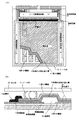
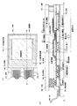
アクティブマトリクス型発光装置の上面図を図1(A)に示す。また、図1(A)中の点線X−X’での断面図を図1(B)に示す。ここでは、白色発光する高分子材料からなる積層構造の発光素子23を一例として説明する。
【0036】
図1(A)および図1(B)中、絶縁表面を有する基板上に設けられた画素部12や駆動回路(ゲート側駆動回路14、15、ソース側駆動回路13)には複数のTFT(図示しない)を有している。なお。画素部12に設けられたTFTは、発光するEL層10に流れる電流を制御する素子であり、第1の電極19や電源供給線16が接続されている。
【0037】
画素部12には、第1の電極19と、第2の電極11と、これらの電極に挟まれた有機化合物を含む層10からなる発光素子23が複数配置され、各発光素子に接続する第1の電極19が規則的に配置されている。第1の電極19は、有機発光素子の陽極(或いは陰極)であり、11は、第2の電極、即ち、有機発光素子の陰極(或いは陽極)である。第2の電極11として透光性の導電材料を用い、第1の電極19として金属材料を用いれば、発光素子23からの光を封止材に通過させて取り出すことができる。一方、第1の電極19として透光性の導電材料を用い、第2の電極として金属材料を用いれば、逆方向に光を取り出すことができる。図1における構成ではどちらの方向でも光の取出しは可能であるが、発光素子23からの光を封止材に通過させて取り出す場合、封止材20および導電性を有する接着剤22として透光性を有することが必須となる。
【0038】
有機化合物を含む層10は積層構造となっている。代表的には、陽極上に正孔輸送層/発光層/電子輸送層という積層構造が挙げられる。この構造は非常に発光効率が高く、現在、研究開発が進められている発光装置は殆どこの構造を採用している。また、他にも陽極上に正孔注入層/正孔輸送層/発光層/電子輸送層、または正孔注入層/正孔輸送層/発光層/電子輸送層/電子注入層の順に積層する構造も良い。発光層に対して蛍光性色素等をドーピングしても良い。また、これらの層は、全て低分子系の材料を用いて形成しても良いし、全て高分子系の材料を用いて形成しても良い。なお、本明細書において、陰極と陽極との間に設けられる全ての層を総称して有機化合物を含む層(EL層)という。したがって、上記正孔注入層、正孔輸送層、発光層、電子輸送層及び電子注入層は、全てEL層に含まれる。また、有機化合物を含む層(EL層)は、シリコンなどの無機材料をも含んでいてもよい。
【0039】
また、第1の電極19の両端部およびそれらの間は有機絶縁物18(障壁またはバンクとも呼ばれる)で覆われている。さらに、有機絶縁物18を無機絶縁膜で覆ってもよい。
【0040】
また、端子部には端子電極が形成されており、端子電極から延びている接続配線17を有している。この接続配線17は、第2の電極11と導電性を有する接着剤22で電気的に接続されている。なお、第2の電極11をマスクとして自己整合的に有機化合物層をエッチングするため、第2の電極11と有機化合物層10の端面は一致し、その端面に接して導電性を有する接着剤22が設けられている。導電性を有する接着剤22は、銀粒子、銅粒子などの導電性微粒子22bとスペーサ22aを含んでおり、さらに、封止材20を接着させて発光素子23を封止している。また、導電性を有する接着剤22としては、熱硬化樹脂を用いてもよいし、紫外線硬化樹脂を用いてもよい。ただし、導電性を有する接着剤22として熱硬化樹脂を用いる場合は、有機化合物を含む層10が変質しない範囲の焼成温度を有する材料を適宜選択する必要があり、また、紫外線硬化樹脂を用いる場合は、封止材として透光性を有する材料を用いる必要がある。
【0041】
また、スペーサ22aは、無機絶縁材料であってもよいし、有機絶縁材料であってもよく、これら粒径の異なる複数種を用いてもよい。また、スペーサ22aとして、金などの低抵抗な金属膜がコートされた無機絶縁材料(例えば、均一粒子径を有するプラスチック微粒子の表面に均一に金メッキを施した導電性微粒子など)とすれば、このスペーサは導電性微粒子と呼べる。
【0042】
また、図1では導電性微粒子22bの径がスペーサ22aの径よりも大きい例を示している。大きい粒径のものを表面に金属膜をコートした弾力性を有する有機材料とし、小さい粒径のものを無機材料として、封止材20を圧着させる際に大きい粒径のものを変形させることによって面接触させてもよい。また、図22に導電性微粒子1022bの径がスペーサ1022aの径よりも小さい例を示す。図22において、第2の電極11と接続配線17の接続部分に存在させて電気的接続が行えればよいため、導電性を有する接着剤1022中に導電性微粒子1022bは均一に分布させる必要はなく、重力によって第2の電極11や接続配線17の近傍付近に密集させればよい。
【0043】
また、導電性を有する接着剤22を用いれば、封止材20を接着させて発光素子23を封止することと、接続配線17と第2の電極11との電気的接続とを同時に行うことができ、スループットを向上させることができる。
【0044】
図1では画素部を覆って全面に導電性を有する接着剤22を形成した例を示したが特に限定されず、部分的に形成してもよい。また、銀ペースト、銅ペースト金ペースト、Pdペーストなどの導電性微粒子を含む材料層と、スペーサやフィラーを含む接着剤との積層としてもよい。積層とする場合には、導電性微粒子を含む材料層の形成によって、先に接続配線17と第2の電極11との電気的接続が行われた後、スペーサやフィラーを含む接着剤を用いて封止材20を接着させて発光素子23を封止することとなる。
【0045】
また、約2〜30μmの間隔が保たれるようにスペーサやフィラーによって封止材20が貼りつけられており、全ての発光素子は密閉されている。ここでは図示しないが、封止材20にはサンドブラスト法などによって凹部が形成されており、その凹部に乾燥剤が配置されている。また、封止材20を貼りつける直前には真空でアニールを行って脱気を行うことが好ましい。また、封止材20を貼りつける際には、不活性気体(希ガスまたは窒素)を含む雰囲気下で行うことが好ましい。
【0046】
また、導電性を有する接着剤の電気抵抗率が比較的に高い場合には、予め封止材20上に電極を形成しておき、貼り合わせる際に導電性を有する接着剤22と電気的に接続させて低抵抗化を行ってもよい。この場合、スペーサ22aとして金などの低抵抗な金属膜がコートされた無機絶縁材料を用いることが好ましく、封止材20との間隔をスペーサ22aの粒径で保持すると同時に、第2の電極11と封止材20上の電極との電気的接続、および接続配線17と封止材20上の電極との電気的接続を行うことができる。また、粒径の異なる複数種を用いる場合には、大きい粒径のものを弾力性を有する有機材料とし、小さい粒径のものを無機材料として、封止材20を圧着させる際に大きい粒径のものを変形させることによって封止材20上の電極と面接触させてもよい。
【0047】
(実施の形態2)
ここでは、導電性を有する接着剤を大面積に形成する図1とは異なる構成例を図2に示す。なお、簡略化のため、図2において、図1と同一である箇所は同一のものを用いる。図2において、第2の電極11までは図1と同一の構成であるため、ここでは詳細な説明を省略する。
【0048】
本実施の形態では、導電材32を部分的に形成し、シール材31を別に形成する例を示す。この導電材32により接続配線17と第2の電極11との電気的接続を行う。なお、第2の電極11をマスクとして自己整合的に有機化合物を含む層をエッチングするため、第2の電極11と有機化合物を含む層10の端面は一致し、その端面に接して導電材32が設けられている。
【0049】
図2において、導電材32としては、銀ペーストや銅ペーストで代表される導電ペーストや導電性インキ、或いはナノメタルインク(粒径5〜10nmのAg、Au、Pdを凝集させずに高濃度で分散した独立分散超微粒子分散液)を用いる。例えば、導電材32として、主成分が銀メッキ銅粉、フェノールレジン、ジメチレングリコールモノメチルエーテルなどからなり、且つ、比抵抗値が5×10⁻⁴Ω・cm以下、接着強度が0.8kg/mm2以上のものを用いればよい。また、導電材32として、速乾性である銀系導電剤(0.5〜1μmの粒径を有する扁平状銀粉末を含む変性ポリオレフィン樹脂)を用いてもよい。
【0050】
導電材32として溶媒を用いている場合は、熱により蒸気が発生して有機化合物を含む層への汚染が懸念されるが、本発明は、導電材32と画素部12との間にシール材31を設けることによって有機化合物を含む層への汚染防止を行っている。従って、シール材31を形成して封止材20と貼り合わせた後、導電材32を形成することが好ましい。なお、シール材31と導電材32の形成順序は特に限定されず、導電材32を形成した後、シール材31を形成して封止材20と貼り合わせてもよい。
【0051】
シール材31にはフィラーが混入されていて、このフィラーによって均一な間隔を持って封止材20が貼り合わせられる。また、フィラーに加えてスペーサを混入させてもよい。また、シール材31は、図2(A)に示すように、ゲート側駆動回路14、15と一部重なるように形成してもよい。
【0052】
また、発光素子23からの光の取出しは、図2における構成においてもどちらの方向も可能である。また、図2の構成においては、画素部の上方に導電材はないので、発光素子23からの光を封止材に通過させて取り出す場合、導電材は不透明な材料を用いてもよいが、封止材20は透光性を有するものとする。
【0053】
また、本実施の形態は実施の形態1と自由に組み合わせることが可能である。
【0054】
(実施の形態3)
ここでは、封止材を貼り合せる図1、図2とは異なる構成例を図3に示す。なお、簡略化のため、図3において、図1と同一である箇所は同一のものを用いる。図3において、第2の電極11までは図1と同一の構成であるため、ここでは詳細な説明を省略する。
【0055】
本実施の形態では、導電材42を部分的に形成し、保護膜で封止する例を示す。この導電材42により接続配線17と第2の電極11との電気的接続を行う。
なお、第2の電極11をマスクとして自己整合的に有機化合物を含む層をエッチングするため、第2の電極11と有機化合物を含む層10の端面は一致し、その端面に接して導電材42が設けられている。
【0056】
上記実施の形態2に示した導電材32と同様に、図3における導電材42としては、銀ペーストや銅ペーストで代表される導電ペーストや導電性インキを用いる。或いは、導電材42としてインクジェット法でのパターン形成が可能なナノメタルインク(粒径5〜10nmのAg、Au、Pdを凝集させずに高濃度で分散した独立分散超微粒子分散液)を用いてもよい。ナノメタルインクは220℃〜250℃で焼成する。
【0057】
導電材42を形成した後、保護膜41を形成する。保護膜41としては、スパッタ法(DC方式やRF方式)により得られる窒化珪素または窒化酸化珪素を主成分とする絶縁膜、またはPCVD法により得られる炭素を主成分とする薄膜である。シリコンターゲットを用い、窒素とアルゴンを含む雰囲気で形成すれば、窒化珪素膜が得られる。また、窒化シリコンターゲットを用いてもよい。また、保護膜41は、リモートプラズマを用いた成膜装置を用いて形成してもよい。また、保護膜に発光を通過させる場合には、保護膜の膜厚は、可能な限り薄くすることが好ましい。
【0058】
本発明において、前記炭素を主成分とする薄膜は膜厚3〜50nmのDLC膜(Diamond like Carbon)であることを特徴としている。DLC膜は短距離秩序的には炭素間の結合として、SP3結合をもっているが、マクロ的にはアモルファス状の構造となっている。DLC膜の組成は炭素が70〜95原子%、水素が5〜30原子%であり、非常に硬く絶縁性に優れている。このようなDLC膜は、また、水蒸気や酸素などのガス透過率が低いという特徴がある。また、微少硬度計による測定で、15〜25GPaの硬度を有することが知られている。
【0059】
DLC膜はプラズマCVD法(代表的には、RFプラズマCVD法、マイクロ波CVD法、電子サイクロトロン共鳴(ECR)CVD法など)、スパッタ法などで形成することができる。いずれの成膜方法を用いても、密着性良くDLC膜を形成することができる。DLC膜は基板をカソードに設置して成膜する。または、負のバイアスを印加して、イオン衝撃をある程度利用して緻密で硬質な膜を形成できる。
【0060】
成膜に用いる反応ガスは、水素ガスと、炭化水素系のガス(例えばCH4、C2H2、C6H6など)とを用い、グロー放電によりイオン化し、負の自己バイアスがかかったカソードにイオンを加速衝突させて成膜する。こうすることにより、緻密で平滑なDLC膜を得ることができる。なお、このDLC膜は、可視光に対して透明もしくは半透明な絶縁膜である。本明細書において、可視光に対して透明とは可視光の透過率が80〜100%であることを指し、可視光に対して半透明とは可視光の透過率が50〜80%であることを指す。
【0061】
また、スパッタ法により透明導電膜からなる膜に接して窒化珪素膜を形成する場合、透明導電膜に含まれる不純物(In、Sn、Zn等)が窒化珪素膜に混入する恐れがあるが、バッファ層となる酸化珪素膜を間に形成することによって窒化珪素膜への不純物混入を防止することもできる。上記構成によりバッファ層を形成することで、透明導電膜からの不純物(In、Snなど)の混入を防止し、不純物のない優れた保護膜を形成することができる。
【0062】
また、保護膜を形成した後に、さらに密閉性を高めるため、シール材を形成して封止材と貼り合わせてもよい。
【0063】
また、本実施の形態は実施の形態1、または実施の形態2と自由に組み合わせることが可能である。
【0064】
(実施の形態4)
ここでは、発光素子の形成手順を簡略に図4を用いて以下に説明する。なお、簡略化のため、図4において、図1と同一である箇所は同一のものを用いる。
【0065】
まず、基板上にTFT(ここでは図示しない)、第1の電極19、接続配線17、絶縁物18を形成した後、スピンコートを用いた塗布法により有機化合物を含む層10を成膜した後、真空加熱で焼成する。(図4(A))なお、有機化合物を含む層を積層する場合には、成膜と焼成を繰り返せばよい。
【0066】
次いで、蒸着マスク50を用いて蒸着法により、選択的に金属材料からなる第2の電極11を形成する。(図4(B))図4(B)において、メタルマスクと有機化合物を含む層との間隔が開いた状態で蒸着を行っている例を示したが、接した状態で行ってもよい。
【0067】
次いで、第2の電極11をマスクとして自己整合的に有機化合物を含む層をエッチングする。ここでは、Ar、H、F、またはOから選ばれた一種または複数種のガスを励起して発生させたプラズマを用いて選択的にエッチングを行う。(図4(C))ただし、第2の電極11がプラズマに耐える材料または膜厚を適宜選択することが重要である。本発明により高分子系材料層の選択的な形成を可能にすることで、外部電源と接続される配線の接続部分に有機化合物を含む層が形成されないような構造を簡単に形成することができる。
【0068】
ここまでの工程で、図4(C)に示す状態が得られるが、この状態では、第2の電極11はどこにも接続されておらず、フローティングになっている。そこで、後の工程で接続配線17と電気的に接続させる。第2の電極11を接続配線17と電気的に接続させる方法としては、上記実施の形態1に示した導電性を有する接着剤22を用いてもよいし、上記実施の形態2および実施の形態3に示した導電材32、42を用いてもよい。
【0069】
本実施の形態では、第2の電極11を接続配線17と電気的に接続させる方法として低抵抗な金属材料からなる第3の電極51を形成する。(図5(B))なお、ここまでの上面図を図5(A)に示す。
【0070】
第3の電極51としては、スパッタ法や蒸着法やPCVD法により適宜形成すればよく、第2の電極11の材料に比べて電気抵抗率が低い金属材料を用いることが好ましい。例えば、第3の電極51として、導電型を付与する不純物元素がドープされたpoly−Si、W、WSiX、Al、Ti、Mo、Cu、Ta、Cr、またはMoから選ばれた元素、または前記元素を主成分とする合金材料もしくは化合物材料を主成分とする膜またはそれらの積層膜からなることを特徴としている。ここでは、前記第3の電極51として、窒化物層またはフッ化物層を最上層とする積層(具体的にはTiNとAlとTiNとの積層)からなる電極とする。従って、発光素子からの光は、第1の電極19を通過させて取り出すこととなる。
【0071】
また、第3の電極51として、第2の電極11と同じ材料を用いてもよく、その場合には、膜厚を第2の電極11の膜厚よりも厚くして低抵抗化を図ることが好ましい。また、第3の電極51として、第2の電極11と同じ材料を用いる場合には、さらに第2の電極11の膜厚を薄くすることもできる。
【0072】
第3の電極51形成以降の工程は、保護膜の形成、或いは封止材を貼り付けて発光素子の封止を行えばよい。
【0073】
また、図5(B)中に示す有機材料からなる絶縁物18の断面形状は重要であるので以下に説明する。絶縁物18上に塗布法により有機化合物膜を形成する場合や、蒸着法で陰極となる金属膜を形成する場合において、絶縁物18の下端部または上端部において曲面を有していない場合、図18に示すように絶縁物18の上端部において凸部が形成されてしまう成膜不良が発生する。そこで、本発明は、図17および図5(B)に示すように絶縁物18の上端部に第1の曲率半径を有する曲面を有し、さらに絶縁物18の下端部に第2の曲率半径を有する曲面を有する形状とすることを特徴としている。なお、第1の曲率半径および第2の曲率半径は、ともに0.2μm〜3μmとすることが好ましい。本発明により、有機化合物膜や金属膜のカバレッジを良好とすることができ、発光領域が減少するシュリンクとよばれる不良も低減することができる。さらに、絶縁膜18上に窒化珪素膜または窒化酸化珪素膜を形成することによってシュリンクを低減することができる。また、絶縁物18の側面におけるテーパー角度は、45°±10°とすればよい。
【0074】
絶縁物18としては、無機材料(酸化シリコン、窒化シリコン、酸化窒化シリコンなど)、感光性または非感光性の有機材料(ポリイミド、アクリル、ポリアミド、ポリイミドアミド、レジストまたはベンゾシクロブテン)、またはこれらの積層などを用いることができるが、図17および図5(B)に示すように絶縁物18の上端部に第1の曲率半径を有する曲面を有し、さらに絶縁物18の下端部に第2の曲率半径を有する曲面を有する形状としたい場合、感光性の有機材料を用いると形成しやすい。また、絶縁物18として、感光性の光によってエッチャントに不溶解性となるネガ型、或いは光によってエッチャントに溶解性となるポジ型のいずれも使用することができる。
【0075】
また、図21に絶縁物68上に窒化珪素膜からなる保護膜70を形成し、絶縁物のパターンと窒化珪素膜のパターンが異なる例を示す。図21は、簡略化のため、有機化合物を含む層60までを形成した段階での上面図を図21(A)に示し、実線A-A'で切断した断面図を図21(B)に示し、実線B−B'で切断した断面図を図21(C)に示した。図21(B)に示した断面図は、隣り合う第1の電極69間に絶縁物68が存在していない。また、図21(A)において、絶縁物68のパターン形状はストライプ形状であり、また、保護膜70である窒化珪素膜のパターンは、点線で示した領域であり、第1の電極69の端部のみを覆う格子形状となっている。絶縁物68をストライプ形状とすることによって、格子状とするよりも第1の電極69表面をウエット洗浄(クリーニング)する際にパーティクルや不純物を除去しやすくすることができる。図21において、画素部62のうち、保護膜70で覆われていない領域が発光領域となる。
【0076】
また、保護膜70として、窒化珪素膜に代えて窒化酸化珪素膜やAlNXOYで示される膜を用いてもよい。なお、AlNXOYで示される膜は、AlNまたはAlからなるターゲットを用いたスパッタ法により、前記ガス導入系から酸素または窒素または希ガスを導入して成膜すればよい。AlNXOYで示される層中に窒素を数atm%以上、好ましくは2.5atm%〜47.5atm%含む範囲であればよく、酸素を47.5atm%以下、好ましくは、0.01〜20atm%未満であればよい。
【0077】
保護膜70を絶縁物68上に形成することによって、有機化合物を含む層60の膜厚均一性が向上し、発光時に生じる電界集中による発熱を抑えることができ、発光領域が減少するシュリンクで代表される発光素子の劣化を防止することができる。
【0078】
また、本実施の形態は実施の形態1乃至3のいずれか一と自由に組み合わせることが可能である。
【0079】
以上の構成でなる本発明について、以下に示す実施例でもってさらに詳細な説明を行うこととする。
【0080】
(実施例)
[実施例1]
本実施例では、EL素子から発した光が素子基板を透過して放射されて観測者の目に入る構造を以下に示す。なお、この場合、観測者は素子基板側から画像を認識することができる。
【0081】
まず、一つの画素に3つのTFTを配置した画素構造を説明する。なお、画素の詳細な上面図の一例を図6に示す。
【0082】
図6に示す構成において、SES駆動をする場合の消去用トランジスタ606を有し、ゲート電極と消去用の信号を入力する第2のゲート信号線603が接続され、ソース電極と電流供給線604が接続され、ドレイン電極とスイッチング用TFT605のドレイン電極・駆動用TFT607のゲート電極が接続されている。
【0083】
3トランジスタ型の場合、スイッチング用TFT605と消去用TFT606の2つのTFTを、第1のゲート信号線602と第2のゲート信号線603の間に、横に並べ直線状に配置する。スイッチング用TFT605のドレイン領域と消去用TFT606のドレイン領域を重ねても良い。この時、スイッチング用TFT605のソース領域のある一点とドレイン領域のある一点と消去用TFT606のソース領域のある一点とドレイン領域のある一点が1つの直線上に並ぶように配置する。
【0084】
上記のように配置することで開口率を上げ、開口部もシンプルな形状にすることが出来る。
【0085】
図6(A)中、α‐α’間の断面を示したものが図6(B)である。駆動用TFT607のように半導体層614を縦方向に蛇行させても良い。半導体層614をこのような形状とすることで、開口率を落とさず、駆動用TFT607のチャネル長Lをより長くすることが出来る。なお、オフ電流値を低減するため、駆動用TFT607として複数のチャネルを有するTFTとしてもよい。また、駆動用TFT607のチャネル長Lは、100μm以上となるようにすることが好ましい。チャネル長Lを長くした場合、酸化膜容量COXが大きくなるため、その容量の一部を有機発光素子の保持容量として利用することができる。従来、1画素毎に保持容量を形成するために保持容量を形成するスペースが必要となり、容量線や容量電極などを設けていたが、本発明の画素構成とすることで容量線や容量電極を省略することができる。また、酸化膜容量COXで保持容量を形成する場合、保持容量は、ゲート絶縁膜を誘電体としてゲート電極と、ゲート絶縁膜を介してゲート電極と重なる半導体とで形成される。従って、TFTのチャネル長を長くしても、図6に示すように画素電極608に接続される駆動用TFT607の半導体層をゲート電極の上層に配置される電流供給線604やソース信号線601の下方に配置すれば、開口率を下げることなく画素設計することができる。即ち、図6に示す画素構成とすることで、容量電極や容量配線を形成するスペースを省略しても十分な保持容量を備えることができ、さらに開口率を上げることができる。さらに、チャネル長Lを長くした場合、レーザー光の照射条件などのTFT製造プロセスのバラツキが生じても、各TFT間の電気特性のバラツキを低減することができる。
【0086】
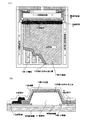
また、図8にアクティブマトリクス型発光装置の外観図について説明する。
なお、図8(A)は、発光装置を示す上面図、図8(B)は図8(A)をA−A’で切断した断面図である。点線で示された901はソース信号線駆動回路、902は画素部、903はゲート信号線駆動回路である。また、904は封止基板、905はシール剤であり、シール剤905で囲まれた内側は、空間907になっている。
【0087】
なお、908はソース信号線駆動回路901及びゲート信号線駆動回路903に入力される信号を伝送するための配線であり、外部入力端子となるFPC(フレキシブルプリントサーキット)909からビデオ信号やクロック信号を受け取る。なお、ここではFPCしか図示されていないが、このFPCにはプリント配線基盤(PWB)が取り付けられていても良い。本明細書における発光装置には、発光装置本体だけでなく、それにFPCもしくはPWBが取り付けられた状態をも含むものとする。
【0088】
次に、断面構造について図8(B)を用いて説明する。基板910上には駆動回路及び画素部が形成されているが、ここでは、駆動回路としてソース信号線駆動回路901と画素部902が示されている。
【0089】
なお、ソース信号線駆動回路901はnチャネル型TFT923とpチャネル型TFT924とを組み合わせたCMOS回路が形成される。また、駆動回路は、公知のCMOS回路、PMOS回路もしくはNMOS回路で形成しても良い。また、本実施の形態では、基板上に駆動回路を形成したドライバー一体型を示すが、必ずしもその必要はなく、基板上ではなく外部に形成することもできる。
【0090】
また、画素部902はスイッチング用TFT911と、電流制御用TFT912とそのドレインに電気的に接続された第1の電極(陽極)913を含む複数の画素により形成される。
【0091】
また、第1の電極(陽極)913の両端には絶縁層914が形成され、第1の電極(陽極)913上には有機化合物を含む層915が形成される。さらに、有機化合物を含む層915上には同一パターン形状であり、端面が一致する第2の電極(陰極)916が形成される。これにより、第1の電極(陽極)913、有機化合物を含む層915、及び第2の電極(陰極)916からなる発光素子918が形成される。ここでは発光素子918は白色発光とする例であるので着色層とBMからなるカラーフィルター(簡略化のため、ここでは図示しない)を基板910に設ける。
【0092】
ここでは、第2の電極916と接続配線908との電気的接続を行うため、実施の形態4に示した第3の電極917を形成する。第2の電極916および接続配線908と接する第3の電極917は、全画素に共通の配線としても機能し、接続配線908を経由してFPC909に電気的に接続されている。
【0093】
また、基板910上に形成された発光素子918を封止するためにシール剤905により封止基板904を貼り合わせる。なお、封止基板904と発光素子918との間隔を確保するために樹脂膜からなるスペーサを設けても良い。そして、シール剤905の内側の空間907には窒素等の不活性気体が充填されている。なお、シール剤905としてはエポキシ系樹脂を用いるのが好ましい。また、シール剤905はできるだけ水分や酸素を透過しない材料であることが望ましい。さらに、空間907の内部に酸素や水を吸収する効果をもつ物質を含有させても良い。
【0094】
また、本実施例では封止基板904を構成する材料としてガラス基板や石英基板の他、FRP(Fiberglass-Reinforced Plastics)、PVF(ポリビニルフロライド)、マイラー、ポリエステルまたはアクリル等からなるプラスチック基板を用いることができる。また、シール剤905を用いて封止基板904を接着した後、さらに側面(露呈面)を覆うようにシール剤で封止することも可能である。
【0095】
以上のようにして発光素子を空間907に封入することにより、発光素子を外部から完全に遮断することができ、外部から水分や酸素といった有機化合物を含む層の劣化を促す物質が侵入することを防ぐことができる。従って、信頼性の高い発光装置を得ることができる。
【0096】
また、上記構造の作製工程の一例を図7に示す。
【0097】
図7(A)は、塗布法による有機化合物膜(PEDOTを含む積層)の形成後、蒸着マスクによって第2の電極(Li−Alからなる陰極)を選択的に形成した段階での断面図である。なお、簡略化のため、透明導電膜からなる陽極やTFTの作製方法はここでは省略する。
【0098】
次いで、図7(B)は、第2の電極をマスクとして自己整合的に有機化合物膜(PEDOTを含む積層)をプラズマでエッチングした段階での断面図である。
【0099】
次いで、図7(C)は、接続配線と接続させるための第3の電極を選択的に形成した段階での断面図である。なお、第2の電極と第3の電極は同じ材料でもよいし、第3の電極の方を電気抵抗率が低い材料を用いてもよい。
【0100】
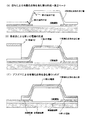
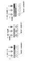
また、本実施例では白色発光素子とカラーフィルターを組み合わせた方法(以下、カラーフィルター法とよぶ)とした例を示した。以下に白色発光素子を形成してフルカラー表示を得る方法を図10(A)で説明する。
【0101】
カラーフィルター法は、白色発光を示す有機化合物膜を有する発光素子を形成し、得られた白色発光をカラーフィルターに通すことで赤、緑、青の発光を得るという方式である。
【0102】
白色発光を得るためには、様々な方法があるが、ここでは塗布により形成可能な高分子材料からなる発光層を用いる場合について説明する。この場合、発光層となる高分子材料への色素ドーピングは溶液調整で行うことができ、複数の色素をドーピングする共蒸着を行う蒸着法に比べて極めて容易に得ることができる。
【0103】
具体的には、仕事関数の大きい金属(Pt、Cr、W、Ni、Zn、Sn、In)からなる陽極上に、正孔注入層として作用するポリ(エチレンジオキシチオフェン)/ポリ(スチレンスルホン酸)水溶液(PEDOT/PSS)を全面に塗布、焼成してPEDOTを含む膜を形成した後、発光層として作用する発光中心色素(1,1,4,4−テトラフェニル−1,3−ブタジエン(TPB)、4−ジシアノメチレン−2−メチル−6−(p−ジメチルアミノ−スチリル)−4H−ピラン(DCM1)、ナイルレッド、クマリン6など)ドープしたポリビニルカルバゾール(PVK)溶液を全面に塗布、焼成した後、仕事関数の小さい金属(Li、Mg、Cs)を含む薄膜と、その上に積層した透明導電膜(ITO(酸化インジウム酸化スズ合金)、酸化インジウム酸化亜鉛合金(In2O3―ZnO)、酸化亜鉛(ZnO)等)との積層からなる陰極を形成する。なお、PEDOT/PSSは溶媒に水を用いており、有機溶剤には溶けない。従って、PVKをその上から塗布する場合にも、再溶解する心配はない。また、PEDOT/PSSとPVKは溶媒が異なるため、成膜室は同一のものを使用しないことが好ましい。
【0104】
また、上記例では図9(B)に示すように有機化合物を含む層を積層とした例を示したが図9(A)に示すように有機化合物を含む層を単層とすることもできる。例えば、ホール輸送性のポリビニルカルバゾール(PVK)に電子輸送性の1,3,4−オキサジアゾール誘導体(PBD)を分散させてもよい。また、30wt%のPBDを電子輸送剤として分散し、4種類の色素(TPB、クマリン6、DCM1、ナイルレッド)を適当量分散することで白色発光が得られる。
【0105】
なお、有機化合物膜は、陽極と陰極の間に形成されており、陽極から注入された正孔と陰極から注入された電子が有機化合物膜において再結合することにより、有機化合物膜において、白色発光が得られる。
【0106】
また、赤色発光する有機化合物膜や緑色発光する有機化合物膜や青色発光する有機化合物膜を適宜選択し、重ねて混色させることによって全体として白色発光を得ることも可能である。
【0107】
以上により形成される有機化合物膜は、全体として白色発光を得ることができる。
【0108】
上記有機化合物膜が白色発光する方向に赤色発光以外を吸収する着色層(R)、緑色発光以外を吸収する着色層(G)、青色発光以外を吸収する着色層(B)をそれぞれ設けたカラーフィルタを形成することにより、発光素子からの白色発光をそれぞれ分離して、赤色発光、緑色発光、青色発光として得ることができる。また、アクティブマトリクス型の場合には、基板とカラーフィルターの間にTFTが形成される構造となる。
【0109】
また、着色層(R,G,B)には、最も単純なストライプパターンをはじめとして、斜めモザイク配列、三角モザイク配列、RGBG四画素配列、もしくはRGBW四画素配列などを用いることができる。
【0110】
白色光源(D65)を用いて各着色層の透過率と波長との関係の一例を図15に示した。カラーフィルターを構成する着色層は、顔料を分散した有機感光材料からなるカラーレジストを用いて形成される。また、白色発光とカラーフィルタを組み合わせた場合の色再現範囲を色度座標として図16に示す。なお、白色発光の色度座標は(x,y)=(0.34、0.35)である。図16よりフルカラーとしての色再現性は十分確保されていることが分かる。
【0111】
なお、この場合には、得られる発光色が異なっていても、すべて白色発光を示す有機化合物膜で形成されていることから、発光色ごとに有機化合物膜を塗り分けて形成する必要がない。また、鏡面反射を防ぐ円偏光板も特に必要ないものとすることができる。
【0112】
次に青色発光性の有機化合物膜を有する青色発光素子と蛍光性の色変換層を組み合わせることにより実現されるCCM法(color changing mediums)について図10(B)により説明する。
【0113】
CCM法は、青色発光素子から出射された青色発光で蛍光性の色変換層を励起し、それぞれの色変換層で色変換を行う。具体的には色変換層で青色から赤色への変換(B→R)、色変換層で青色から緑色への変換(B→G)、色変換層で青色から青色への変換(B→B)(なお、青色から青色への変換は行わなくても良い。)を行い、赤色、緑色及び青色の発光を得るというものである。CCM法の場合にも、アクティブマトリクス型の場合には、基板と色変換層の間にTFTが形成される構造となる。
【0114】
なお、この場合にも有機化合物膜を塗り分けて形成する必要がない。また、鏡面反射を防ぐ円偏光板も特に必要ないものとすることができる。
【0115】
また、CCM法を用いる場合には、色変換層が蛍光性であるため外光により励起され、コントラストを低下させる問題があるので、図10(C)に示したようにカラーフィルターを装着するなどしてコントラストを上げるようにすると良い。図10(C)には白色発光素子を用いる例を示したが青色発光素子を用いても良い。
【0116】
また、図9(C)に示すように、有機化合物を含む層として高分子材料からなる層と、低分子材料からなる層とを積層しても白色発光を得ることができる。積層で白色発光とする場合には、正孔注入層となる高分子材料を塗布法で形成した後、蒸着法で共蒸着を行い、発光性領域における発光と発光色が異なる色素を正孔輸送層中にドーピングして、発光性領域からの発光色と混色させればよい。適宜、発光層や正孔輸送層の材料を調節することによって全体として白色発光を得ることができる。
【0117】
また、電極をマスクとして、高分子材料からなる有機化合物を含む層をプラズマによって自己整合的にエッチングする本発明は、白色発光に限らず、有機化合物を含む層として高分子材料を少なくとも一層用いる有色発光素子にも適用できる。
【0118】
図11に発光素子の積層構造の一例を示す。
【0119】
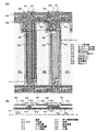
図11(A)に示した積層構造は、陽極701上に、高分子系材料からなる第1の有機化合物を含む層702aと低分子系材料からなる第2の有機化合物を含む層702bとの積層である有機化合物を含む層702と、陰極バッファー層703と、陰極704とが形成されたものである。陰極と陽極で挟まれるこれらの層の材料および膜厚を適宜設定することで、赤色、緑色、青色の発光素子を得ることができる。
【0120】
赤色の発光素子を得る場合、図11(B)に示したようにITOからなる陽極上に高分子系材料であるPEDOT/PSSをスピンコートで塗布し、真空ベークで焼成して膜厚30nmとする。次いで、4,4'−ビス[N−(1−ナフチル)−N−フェニル−アミノ]−ビフェニル(以下、α−NPDと示す)を蒸着法で膜厚60nm形成する。次いで、ドーパントとしてDCMを含むトリス(8−キノリノラト)アルミニウム(以下、Alq3と示す)を蒸着法で膜厚40nm形成する。次いで、Alq3を膜厚40nm形成する。次いで、CaF2を蒸着法で膜厚1nm形成した後、最後にAlをスパッタ法または蒸着法により膜厚200nm形成することによって赤色の発光素子を完成させる。
【0121】
また、緑色の発光素子を得る場合、図11(C)に示したようにITOからなる陽極上に高分子系材料であるPEDOT/PSSをスピンコートで塗布し、真空ベークで焼成して膜厚30nmとする。次いで、α−NPDを蒸着法で膜厚60nm形成する。次いで、ドーパントとしてDMQDを含むAlq3を共蒸着で膜厚40nm形成する。次いで、Alq3を膜厚40nm形成する。次いで、CaF2を蒸着法で膜厚1nm形成した後、最後にAlをスパッタ法または蒸着法により膜厚200nm形成することによって緑色の発光素子を完成させる。
【0122】
また、青色の発光素子を得る場合、図11(D)に示したようにITOからなる陽極上に高分子系材料であるPEDOT/PSSをスピンコートで塗布し、真空ベークで焼成して膜厚30nmとする。次いで、α−NPDを蒸着法で膜厚60nm形成する。次いで、ドーパントとしてバソキュプロイン(以下、BCPと示す)を蒸着法で膜厚10nm形成する。次いで、Alq3を膜厚40nm形成する。次いで、CaF2を蒸着法で膜厚1nm形成した後、最後にAlをスパッタ法または蒸着法により膜厚200nm形成することによって青色の発光素子を完成させる。
【0123】
上記有色発光素子(R、G、B)を形成する場合には、カラーフィルターを設ける必要はなくなるが、色純度を上げるために設けてもよい。
【0124】
また、本実施例は、実施の形態1乃至4のいずれとも自由に組み合わせることができる。
【0125】
[実施例2]
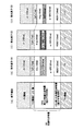
本実施例では発光素子の形成から封止までの作製を全自動化したマルチチャンバー方式の製造装置の例を図12に示す。
【0126】
図12において、100a〜100k、100m〜100wはゲート、101は仕込室、119は取出室、102、104a、108、114、118は搬送室、105、107、111は受渡室、106R、106B、106G、106H、106E、109、110、112、113は成膜室、103は前処理室、117は封止基板ロード室、115はディスペンサ室、116は封止室、120a、120bはカセット室、121はトレイ装着ステージ、122はプラズマによるエッチング室である。
【0127】
まず、予め複数のTFT、透明導電膜(ITO(酸化インジウム酸化スズ合金)、酸化インジウム酸化亜鉛合金(In2O3―ZnO)、酸化亜鉛(ZnO)等)からなる陽極(第1の電極)、陽極の端部を覆う絶縁物が設けられた基板上に、正孔注入層として作用するポリ(エチレンジオキシチオフェン)/ポリ(スチレンスルホン酸)水溶液(PEDOT/PSS)を全面に形成し、真空中での加熱処理を行って水分を気化させる。なお、陽極の表面をクリーニングまたは研磨する必要があれば、PEDOTを含む有機化合物層を形成する前に行えばよい。
【0128】
以下、予めTFT、陽極、陽極の端部を覆う絶縁物、及び正孔注入層(PEDOT)が設けられた基板を図12に示す製造装置に搬入し、図9(B)に示す積層構造を形成する手順を示す。
【0129】
まず、カセット室120aまたはカセット室120bに上記基板をセットする。基板が大型基板(例えば300mm×360mm)である場合には、カセット室120bにセットし、通常基板(例えば、127mm×127mm)である場合には、トレイ装着ステージ121に搬送し、トレイ(例えば300mm×360mm)に数枚の基板を搭載する。
【0130】
次いで、カセット室120bから基板搬送機構が設けられた搬送室118に搬送する。次いで、成膜室112に搬送し、全面に設けられた正孔注入層(PEDOT)上に、発光層となる高分子からなる有機化合物層を全面に形成する。成膜室112は、高分子からなる有機化合物層を形成するための成膜室である。本実施例では、発光層として作用する色素(1,1,4,4−テトラフェニル−1,3−ブタジエン(TPB)、4−ジシアノメチレン−2−メチル−6−(p−ジメチルアミノ−スチリル)−4H−ピラン(DCM1)、ナイルレッド、クマリン6などをドープしたポリビニルカルバゾール(PVK)溶液を全面に形成する例を示す。成膜室112においてスピンコート法で有機化合物層を形成する場合には、大気圧下で基板の被成膜面を上向きにしてセットする。また、水や有機溶剤を溶媒として用いた成膜を行った後は、真空中での加熱処理を行って水分を気化させることが好ましく、成膜室112に連結する真空加熱可能なアニール室を設けてもよい。
【0131】
次いで、基板搬送機構が設けられた搬送室118から仕込室101に搬送する。
【0132】
仕込室101は、真空排気処理室と連結されており、真空排気した後、不活性ガスを導入して大気圧にしておくことが好ましい。次いで仕込室101に連結された搬送室102に搬送する。予め、搬送室内には極力水分や酸素が存在しないよう、真空排気して真空を維持しておく。
【0133】
また、搬送室102には、搬送室内を真空にする真空排気処理室と連結されている。真空排気処理室としては、磁気浮上型のターボ分子ポンプ、クライオポンプ、またはドライポンプが備えられている。これにより搬送室の到達真空度を10-5〜10-6Paにすることが可能であり、さらにポンプ側および排気系からの不純物の逆拡散を制御することができる。装置内部に不純物が導入されるのを防ぐため、導入するガスとしては、窒素や希ガス等の不活性ガスを用いる。装置内部に導入されるこれらのガスは、装置内に導入される前にガス精製機により高純度化されたものを用いる。従って、ガスが高純度化された後に成膜装置に導入されるようにガス精製機を備えておく必要がある。これにより、ガス中に含まれる酸素や水、その他の不純物を予め除去することができるため、装置内部にこれらの不純物が導入されるのを防ぐことができる。
【0134】
また、水や有機溶剤を溶媒として用いた成膜を行った後は、前処理室103に搬送し、そこで高真空中での加熱処理を行ってさらに水分を気化させることが好ましい。
【0135】
本実施例では、高分子材料からなる有機化合物層を積層した例を示したが、図9(C)や図11に示す低分子材料からなる層との積層構造とする場合には、適宜、蒸着法により成膜室106R、106G、106Bで成膜を行って、発光素子全体として、白色、或いは赤色、緑色、青色の発光を示す有機化合物を含む層を適宜形成すればよい。受渡室105には、基板反転機構が備わっており、基板を適宜反転させる。
【0136】
また、必要があれば、適宜、成膜室106Eで電子輸送層または電子注入層、106Hで正孔注入層または正孔輸送層を形成すればよい。蒸着法を用いる場合、例えば、真空度が5×10⁻³Torr(0.665Pa)以下、好ましくは10-4〜10-6Paまで真空排気された成膜室で蒸着を行う。蒸着の際、予め、抵抗加熱により有機化合物は気化されており、蒸着時にシャッター(図示しない)が開くことにより基板の方向へ飛散する。気化された有機化合物は、上方に飛散し、メタルマスク(図示しない)に設けられた開口部(図示しない)を通って基板に蒸着される。なお、蒸着の際、基板を加熱する手段により基板の温度(T1)は、50〜200℃、好ましくは65〜150℃とする。また、蒸着法を用いる場合、成膜室には蒸着材料が予め材料メーカーで収納されているルツボをセットすることが好ましい。セットする際には大気に触れることなく行うことが好ましく、材料メーカーから搬送する際、ルツボは第2の容器に密閉した状態のまま成膜室に導入することが好ましい。望ましくは、成膜室106Rに連結して真空排気手段を有するチャンバーを備え、そこで真空、若しくは不活性ガス雰囲気で第2の容器からルツボを取り出して、成膜室にルツボを設置する。こうすることによって、ルツボおよび該ルツボに収納されたEL材料を汚染から防ぐことができる。
【0137】
次いで、大気にふれさせることなく、搬送室102から受渡室105へ、受渡室105から搬送室104aへ、さらに搬送室104aから受渡室107に基板を搬送した後、さらに、大気にふれさせることなく、受渡室107から搬送室108に基板を搬送する。
【0138】
次いで、搬送室108内に設置されている搬送機構によって、成膜室110に搬送し、金属膜(MgAg、MgIn、AlLi、CaF2、CaNなどの合金、または周期表の1族もしくは2族に属する元素とアルミニウムとを共蒸着法により形成した膜)からなる陰極(第2の電極)を抵抗加熱を用いた蒸着法で形成する。蒸着の際には蒸着マスクを用いて選択的に形成する。
【0139】
次いで、搬送室108内に設置されている搬送機構によって、プラズマ処理室122に搬送し、第2の電極をマスクとして高分子材料からなる有機化合物膜の積層を自己整合的に除去する。プラズマ処理室122はプラズマ発生手段を有しており、Ar、H、F、またはOから選ばれた一種または複数種のガスを励起してプラズマを発生させることによって、ドライエッチングを行う。酸素プラズマ処理でエッチングするのであれば、前処理室103でも行うことが可能である。
【0140】
次いで、再度、成膜室110に搬送し、金属膜(MgAg、MgIn、AlLi、CaNなどの合金、または周期表の1族もしくは2族に属する元素とアルミニウムとを共蒸着法により形成した膜)からなる第3の電極(陰極の上層とも言える)を抵抗加熱を用いた蒸着法で形成する。なお、ここでは、先に蒸着を行った金属膜の蒸着マスクとは異なるマスクを用い、第3の電極を形成することによって、第2の電極と接続配線との電気的接続を行う。本実施例では、同じ成膜室110で第2の電極と第3の電極を形成する例を示したが、マスク交換が必要とされるので効率が落ちる。従って、タスクを向上するために成膜室をそれぞれ別に設けることが好ましい。なお、本実施例では蒸着マスクで選択的に第3の電極の形成を行う例を示したが、スパッタ法で金属膜を形成した後、フォトレジストを用いてエッチングを行うパターニングを行ってもよい。
【0141】
以上の工程で図9(B)に示す積層構造の発光素子が形成される。
【0142】
次いで、大気に触れることなく、搬送室108から成膜室113に搬送して窒化珪素膜、または窒化酸化珪素膜からなる保護膜を形成する。ここでは、成膜室113内に、珪素からなるターゲット、または酸化珪素からなるターゲット、または窒化珪素からなるターゲットを備えたスパッタ装置とする。例えば、珪素からなるターゲットを用い、成膜室雰囲気を窒素雰囲気または窒素とアルゴンを含む雰囲気とすることによって窒化珪素膜を形成することができる。
【0143】
次いで、発光素子が形成された基板を大気に触れることなく、搬送室108から受渡室111に搬送し、さらに受渡室111から搬送室114に搬送する。
【0144】
次いで、発光素子が形成された基板を搬送室114から封止室116に搬送する。なお、封止室116には、シール材が設けられた封止基板を用意しておくことが好ましい。
【0145】
封止基板は、封止基板ロード室117に外部からセットされる。なお、水分などの不純物を除去するために予め真空中でアニール、例えば、封止基板ロード室117内でアニールを行うことが好ましい。そして、封止基板にシール材を形成する場合には、搬送室114を大気圧とした後、封止基板を封止基板ロード室からディスペンサ室115に搬送して、発光素子が設けられた基板と貼り合わせるためのシール材を形成し、シール材を形成した封止基板を封止室116に搬送する。
【0146】
次いで、発光素子が設けられた基板を脱気するため、真空または不活性雰囲気中でアニールを行った後、シール材が設けられた封止基板と、発光素子が形成された基板とを貼り合わせる。また、密閉された空間には水素または不活性気体を充填させる。なお、ここでは、封止基板にシール材を形成した例を示したが、特に限定されず、発光素子が形成された基板にシール材を形成してもよい。
【0147】
次いで、貼り合わせた一対の基板を封止室116に設けられた紫外線照射機構によってUV光を照射してシール材を硬化させる。なお、ここではシール材として紫外線硬化樹脂を用いたが、接着材であれば、特に限定されない。
【0148】
次いで、貼り合わせた一対の基板を封止室116から搬送室114、そして搬送室114から取出室119に搬送して取り出す。
【0149】
以上のように、図12に示した製造装置を用いることで完全に発光素子を密閉空間に封入するまで外気に晒さずに済むため、信頼性の高い発光装置を作製することが可能となる。なお、搬送室114においては、真空と、大気圧での窒素雰囲気とを繰り返すが、搬送室102、104a、108は常時、真空が保たれることが望ましい。
【0150】
なお、インライン方式の成膜装置とすることも可能である。
【0151】
また、図12に示す製造装置に搬入し、陽極として金属膜(仕事関数の大きい金属(Pt、Cr、W、Ni、Zn、Sn、Inなど))を用い、上記積層構造による発光方向とは逆方向である発光素子を形成する手順を以下に示す。
【0152】
まず、予め複数のTFT、陽極、陽極の端部を覆う絶縁物が設けられた基板上に、正孔注入層として作用するポリ(エチレンジオキシチオフェン)/ポリ(スチレンスルホン酸)水溶液(PEDOT/PSS)を全面に形成し、真空中での加熱処理を行って水分を気化させる。
【0153】
次いで、カセット室120aまたはカセット室120bにTFT及び陽極が設けられた基板をセットする。
【0154】
次いで、カセット室から基板搬送機構が設けられた搬送室118に搬送する。
【0155】
次いで、成膜室112に搬送し、全面に設けられた正孔注入層(PEDOT)上に、発光層となる高分子からなる有機化合物層を全面に形成する。成膜室112は、高分子からなる有機化合物層を形成するための成膜室である。本実施例では、発光層として作用する色素(1,1,4,4−テトラフェニル−1,3−ブタジエン(TPB)、4−ジシアノメチレン−2−メチル−6−(p−ジメチルアミノ−スチリル)−4H−ピラン(DCM1)、ナイルレッド、クマリン6など)ドープしたポリビニルカルバゾール(PVK)溶液を全面に形成する例を示す。成膜室112においてスピンコート法で有機化合物層を形成する場合には、大気圧下で基板の被成膜面を上向きにしてセットする。
【0156】
次いで、基板搬送機構が設けられた搬送室118から仕込室101に搬送する。
次いで仕込室101に連結された搬送室102に搬送する。なお、水や有機溶剤を溶媒として用いた成膜を行った後は、前処理室103に搬送し、そこで真空中での加熱処理を行って水分を気化させることが好ましい。
【0157】
次いで、大気にふれさせることなく、搬送室102から受渡室105へ、受渡室105から搬送室104aへ、さらに搬送室104aから受渡室107に基板を搬送した後、さらに、大気にふれさせることなく、受渡室107から搬送室108に基板を搬送する。
【0158】
次いで、搬送室108内に設置されている搬送機構によって、成膜室110に搬送し、非常に薄い金属膜(MgAg、MgIn、AlLi、CaNなどの合金、または周期表の1族もしくは2族に属する元素とアルミニウムとを共蒸着法により形成した膜)からなる陰極(下層)を抵抗加熱を用いた蒸着法で形成する。薄い金属層からなる陰極(下層)を形成した後、成膜室109に搬送してスパッタ法により透明導電膜(ITO(酸化インジウム酸化スズ合金)、酸化インジウム酸化亜鉛合金(In2O3―ZnO)、酸化亜鉛(ZnO)等)からなる陰極(上層)を形成し、薄い金属層と透明導電膜との積層からなる陰極(第2の電極)をメタルマスクなどを用いて適宜形成する。
【0159】
次いで、搬送室108内に設置されている搬送機構によって、プラズマ処理室122に搬送し、第2の電極をマスクとして高分子材料からなる有機化合物膜の積層を自己整合的に除去する。プラズマ処理室122はプラズマ発生手段を有しており、Ar、H、F、またはOから選ばれた一種または複数種のガスを励起してプラズマを発生させることによって、ドライエッチングを行う。酸素プラズマ処理でエッチングするのであれば、前処理室103でも行うことが可能である。
【0160】
次いで、再度、成膜室109に搬送し、透明導電膜からなる第3の電極(陰極の上層とも言える)をスパッタ法で形成する。なお、ここでは、メタルマスクを換え、先に形成した第2の電極パターンとは異なるパターンとし、第3の電極を形成することによって、第2の電極と接続配線との電気的接続を行う。なお、本実施例ではマスクで選択的に第3の電極の形成を行う例を示したが、フォトレジストを用いてエッチングを行うパターニングを行ってもよい。
【0161】
以上の工程で第2の電極を通過させて光を取り出す発光素子が形成される。
【0162】
また、以降の工程は、上記した図9(B)に示す積層構造を有する発光装置の作製手順と同一であるのでここでは説明を省略する。
【0163】
なお、本実施例では、第3の電極を形成することによって、第2の電極と接続配線との電気的接続を行う実施の形態4に示した方法を用いた例を示したが、特に限定されず、実施の形態1乃至3のいずれか一に示した方法で第2の電極と接続配線との電気的接続を行ってもよい。
【0164】
また、本実施例は実施例1と自由に組み合わせることができる。
【0165】
[実施例3]
本発明を実施することによって有機発光素子を有するモジュール(アクティブマトリクス型ELモジュール)を組み込んだ全ての電子機器が完成される。
【0166】
その様な電子機器としては、ビデオカメラ、デジタルカメラ、ヘッドマウントディスプレイ(ゴーグル型ディスプレイ)、カーナビゲーション、プロジェクタ、カーステレオ、パーソナルコンピュータ、携帯情報端末(モバイルコンピュータ、携帯電話または電子書籍等)などが挙げられる。それらの一例を図13、図14に示す。
【0167】
図13(A)はパーソナルコンピュータであり、本体2001、画像入力部2002、表示部2003、キーボード2004等を含む。
【0168】
図13(B)はビデオカメラであり、本体2101、表示部2102、音声入力部2103、操作スイッチ2104、バッテリー2105、受像部2106等を含む。
【0169】
図13(C)はモバイルコンピュータ(モービルコンピュータ)であり、本体2201、カメラ部2202、受像部2203、操作スイッチ2204、表示部2205等を含む。
【0170】
図13(D)はゴーグル型ディスプレイであり、本体2301、表示部2302、アーム部2303等を含む。
【0171】
図13(E)はプログラムを記録した記録媒体(以下、記録媒体と呼ぶ)を用いるプレーヤーであり、本体2401、表示部2402、スピーカ部2403、記録媒体2404、操作スイッチ2405等を含む。なお、このプレーヤーは記録媒体としてDVD(Digtial Versatile Disc)、CD等を用い、音楽鑑賞や映画鑑賞やゲームやインターネットを行うことができる。
【0172】
図13(F)はデジタルカメラであり、本体2501、表示部2502、接眼部2503、操作スイッチ2504、受像部(図示しない)等を含む。
【0173】
図14(A)は携帯電話であり、本体2901、音声出力部2902、音声入力部2903、表示部2904、操作スイッチ2905、アンテナ2906、画像入力部(CCD、イメージセンサ等)2907等を含む。
【0174】
図14(B)は携帯書籍(電子書籍)であり、本体3001、表示部3002、3003、記憶媒体3004、操作スイッチ3005、アンテナ3006等を含む。
【0175】
図14(C)はディスプレイであり、本体3101、支持台3102、表示部3103等を含む。
【0176】
ちなみに図14(C)に示すディスプレイは中小型または大型のもの、例えば5〜20インチの画面サイズのものである。また、このようなサイズの表示部を形成するためには、基板の一辺が1mのものを用い、多面取りを行って量産することが好ましい。
【0177】
以上の様に、本発明の適用範囲は極めて広く、あらゆる分野の電子機器の作製方法に適用することが可能である。また、本実施例の電子機器は実施の形態1乃至4、実施例1、および実施例2のどのような組み合わせからなる構成を用いても実現することができる。
【0178】
[実施例4]
実施の形態4では、第1及び第2の曲率半径を有する絶縁物の例を示したが、本実施例では、絶縁物の上端部のみに曲率半径を有する例を図19に示す。
【0179】
また、本実施例において、絶縁物以外の構成は、実施の形態4と同一としているが特に限定されず、実施の形態1乃至3に示す絶縁物に代えて、本実施例に示す絶縁物を適用することができる。
【0180】
図19中、80は有機化合物を含む層、81は第2の電極、87は接続配線、88は絶縁物、89は第1の電極、91は第3の電極、93は発光素子である。絶縁物88としては、光によってエッチャントに不溶解性となるネガ型有機材料、或いは光によってエッチャントに溶解性となるポジ型有機材料を用いることが好ましい。
【0181】
本実施例では絶縁物88をポジ型のフォトレジストを用いて形成する。露光条件やエッチャント条件などを調節することによって、図19(A)に示す絶縁物88を形成する。絶縁物88において、上端部のみに曲率半径0.2μm〜3μmを有している。絶縁物88により、有機化合物を含む層80や金属膜からなる第2の電極81のカバレッジを良好とすることができ、発光領域が減少するシュリンクとよばれる不良も低減することができる。なお、ガラス基板上にポジ型のアクリル樹脂を用いて図19(A)に示す絶縁物88と同様の形状を形成し、断面を観察した写真が図20である。また、絶縁物88の側面におけるテーパー角度は、45°±10°とすればよい。
【0182】
また、図19(B)では絶縁物として、感光性有機材料であるフォトレジストからなる上層98bと非感光性有機材料であるアクリルからなる下層98aの積層とする例を示す。絶縁物の上層98bにおいて、上端部のみに曲率半径0.2μm〜3μmを有している。下層98aとしては、非感光性材料に代えて、無機材料(酸化シリコン、窒化シリコン、酸化窒化シリコンなど)を用いることができる。
【0183】
また、図19(C)では絶縁物88上にRFスパッタ法で窒化珪素膜94を形成した例である。窒化珪素膜94に代えて窒化酸化珪素膜やAlNXOYで示される膜を用いてもよい。なお、AlNXOYで示される膜は、AlNまたはAlからなるターゲットを用いたスパッタ法により、前記ガス導入系から酸素または窒素または希ガスを導入して成膜すればよい。AlNXOYで示される層中に窒素を数atm%以上、好ましくは2.5atm%〜47.5atm%含む範囲であればよく、酸素を47.5atm%以下、好ましくは、0.01〜20atm%未満であればよい。窒化珪素膜などの保護膜を絶縁物88に形成することによって、発光領域が減少するシュリンクとよばれる不良も低減することができる。
【0184】
また、本実施例は実施の形態1乃至4、実施例1乃至3のどのような組み合わせも可能である。
【0185】
【発明の効果】
本発明により、高分子系材料層の選択的な形成を可能にすることで、外部電源と接続される配線の接続部分に有機化合物を含む層が形成されないような構造を簡単に形成することができる。
【0186】
また、本発明により、カラーフィルタを設けることによって円偏光板を不必要としコストを低減するとともに、塗りわけが必要でなくなるため、スループットの向上および高精細化も実現可能としている。
【図面の簡単な説明】
【図1】 断面図および上面図を示す図。(実施の形態1)
【図2】 断面図および上面図を示す図。(実施の形態2)
【図3】 断面図および上面図を示す図。(実施の形態3)
【図4】 エッチング工程を示す図。(実施の形態4)
【図5】 断面図および上面図を示す図。(実施の形態4)
【図6】 画素上面図を示す図である。(実施例1)
【図7】 工程図を示す図である。(実施例1)
【図8】 アクティブ型表示装置の断面図および上面図。(実施例1)
【図9】 発光素子の積層構造を示す図である。(実施例1)
【図10】 白色発光を用いてフルカラー化する場合の模式図である。(実施例1)
【図11】 高分子材料と低分子材料の積層でフルカラー化する場合の模式図である。(実施例1)
【図12】 製造装置を示す図である。(実施例2)
【図13】 電子機器の一例を示す図。(実施例3)
【図14】 電子機器の一例を示す図。(実施例3)
【図15】 着色層の透過率を示す図。(実施例1)
【図16】 色度座標を示す図。(実施例1)
【図17】 絶縁物周辺の断面を示す写真図。(実施の形態4)
【図18】 絶縁物周辺の断面を示す写真図。(比較例)
【図19】 断面図を示す図。(実施例4)
【図20】 絶縁物周辺の断面を示す写真図。
【図21】 断面図および上面図を示す図。(実施の形態4)
【図22】 断面図を示す図。(実施の形態1)[0001]
BACKGROUND OF THE INVENTION
The present invention relates to a light-emitting device using a light-emitting element in which fluorescence or phosphorescence is obtained by applying an electric field to an element in which a film containing an organic compound is provided between a pair of electrodes, and a manufacturing method thereof. Note that a light-emitting device in this specification refers to an image display device, a light-emitting device, or a light source (including a lighting device). Also, a module in which a connector such as an FPC (Flexible printed circuit) or TAB (Tape Automated Bonding) tape or TCP (Tape Carrier Package) is attached to the light emitting device, or a module in which a printed wiring board is provided at the end of the TAB tape or TCP In addition, a module in which an IC (integrated circuit) is directly mounted on a light emitting element by a COG (Chip On Glass) method is also included in the light emitting device.
[0002]
[Prior art]
A light-emitting element using an organic compound having characteristics such as thin and light weight, high-speed response, and direct current low-voltage driving as a light emitter is expected to be applied to a next-generation flat panel display. In particular, a display device in which light emitting elements are arranged in a matrix is considered to be superior to a conventional liquid crystal display device in that it has a wide viewing angle and excellent visibility.
[0003]
The light-emitting mechanism of a light-emitting element is such that electrons injected from a cathode and holes injected from an anode emit light in a layer containing an organic compound by applying a voltage with a layer containing the organic compound sandwiched between a pair of electrodes. It is said that it recombines at the center to form a molecular exciton, which emits energy and emits light when the molecular exciton returns to the ground state. Singlet excitation and triplet excitation are known as excited states, and light emission is considered to be possible through either excited state.
[0004]
For a light-emitting device formed by arranging such light-emitting elements in a matrix, driving methods such as passive matrix driving (simple matrix type) and active matrix driving (active matrix type) can be used. However, when the pixel density increases, the active matrix type in which a switch is provided for each pixel (or one dot) is considered to be advantageous because it can be driven at a lower voltage.
[0005]
In addition, organic compounds that can be said to be the center of a light-emitting element, which is a layer containing an organic compound (strictly, a light-emitting layer), have been studied for low-molecular materials and polymer-based materials. Attention has been focused on polymer materials that are easier to handle and have higher heat resistance than system materials.
[0006]
As a method for forming these organic compounds, a method such as a vapor deposition method, a spin coating method, and an ink jet method is known. As a method for realizing full color using a polymer material, a spin method is used. Coating methods and ink jet methods are particularly well known.
[0007]
However, when the spin coating method is used, an organic compound is formed on the entire film formation surface. Therefore, an organic compound is formed only at a position where film formation is desired and a film is not formed at a place where film formation is not required. Film formation is difficult.
[0008]
Further, in an active matrix light-emitting device, a driving circuit formed on a substrate is formed with wiring for inputting an electrical signal from an external power source, and a cathode, an anode, and an organic compound formed in a pixel portion. Since the wiring for electrically connecting the light emitting element composed of the layer containing the organic compound and the external power supply is formed, the organic compound is formed in the connection portion (terminal portion) of these wirings to the external power supply If this is done, there is a problem that an ohmic contact with the external power source cannot be obtained. In particular, when a layer containing an organic compound is formed using a spin coating method, it is difficult to route an electrode (cathode or anode) provided on the layer containing the organic compound to the terminal portion.
[0009]
[Problems to be solved by the invention]
Therefore, the present invention provides a method for selectively forming a polymer organic compound layer, and an electrode (cathode or anode) provided on the organic compound layer is electrically connected to a wiring extending from the terminal portion. Provide a connection structure to be connected.
[0010]
In addition, an ink-jet method known as a method for selectively forming a polymer organic compound can coat organic compounds emitting three types (R, G, B) at a time. Since the film accuracy is poor and it is difficult to control, uniformity cannot be obtained and variations tend to occur. Causes of variations in the ink jet method include variations in nozzle pitch, variations in ink flight curve, stage alignment accuracy, timing variations in ink ejection and stage movement, and the like. For example, implementation conditions such as clogging an inkjet nozzle due to an internal viscosity resistance of an ink prepared by dissolving an organic compound in a solvent, or ink ejected from the nozzle does not land at a desired position And a problem in practical use in which a dedicated device having a high-precision stage, an automatic alignment mechanism, an ink head, and the like is required and costs are increased. In addition, since ink spreads after landing, a certain margin is required as an interval between adjacent pixels, which makes high definition difficult.
[0011]
Therefore, the present invention provides a method for selectively forming a polymer material layer that is simpler than the case of using an inkjet method in an active matrix light-emitting device using a polymer organic compound, and Another object of the present invention is to easily form a structure in which an organic compound layer is not formed at a connection portion of a wiring connected to an external power source.
[0012]
In the light emitting device, the incident external light (light outside the light emitting device) is reflected by the back surface of the cathode (the surface in contact with the light emitting layer) at the non-light emitting pixel, and the back surface of the cathode acts like a mirror. Then, there was a problem that the external scenery was reflected on the observation surface (the surface facing the observer). In addition, in order to avoid this problem, a device has been devised to attach a circularly polarizing film on the observation surface of the light emitting device so that no external scenery is reflected on the observation surface, but the circularly polarizing film is very expensive. For this reason, there is a problem in that the manufacturing cost is increased.
[0013]
[Means for Solving the Problems]
In the present invention, after a film made of a polymer material is formed on the entire surface of the lower electrode (first electrode) by a coating method, the upper electrode (second electrode) is formed by a vapor deposition method using a vapor deposition mask. The film made of the polymer material is etched in a self-aligned manner by plasma etching using the upper electrode as a mask, and the polymer material layer can be selectively formed.
[0014]
Further, an auxiliary electrode (third electrode) is formed to connect the upper electrode to the wiring extending to the terminal electrode. Further, the upper electrode may be made thin as long as it can withstand the etching process by plasma, and the resistance may be lowered by an auxiliary electrode formed thereon. The auxiliary electrode may be a metal wiring made of a metal material, or a conductive paste (nano paste, hybrid paste, nano metal ink, etc.) or an adhesive containing conductive fine particles.
[0015]
The configuration of the invention disclosed in this specification is, as shown in FIG. 1 and FIG.
Between the first substrate having an insulating surface and the second substrate having a light-transmitting property, a first electrode, a layer containing an organic compound in contact with the first electrode, and a layer containing the organic compound A light emitting device having a pixel portion having a plurality of light emitting elements having a second electrode in contact therewith, a drive circuit, and a terminal portion,
The terminal portion is disposed on the first substrate so as to be located outside the second substrate;
The first substrate and the second substrate are bonded by an adhesive in which a plurality of kinds of conductive fine particles having different diameters are mixed, and the second electrode and the wiring from the terminal portion are electrically connected. The light-emitting device is characterized in that the light-emitting devices are connected to each other.
[0016]
In addition, as shown in FIG.
Between the first substrate having an insulating surface and the second substrate having a light-transmitting property, a first electrode, a layer containing an organic compound in contact with the first electrode, and a layer containing the organic compound A light emitting device having a pixel portion having a plurality of light emitting elements having a second electrode in contact therewith, a drive circuit, and a terminal portion,
The terminal portion is disposed on the first substrate so as to be located outside the second substrate;
The first substrate and the second substrate are bonded by an adhesive in which fine particles made of an inorganic material and conductive fine particles having a diameter larger than the fine particles are mixed, and the second electrode; A light-emitting device characterized in that wiring from a terminal portion is electrically connected.
[0017]
In addition, as shown in FIG. 2 and FIG.
A pixel portion including a plurality of light-emitting elements each including a first electrode, a layer containing an organic compound in contact with the first electrode, and a second electrode in contact with the layer containing the organic compound; and a terminal portion. A light emitting device comprising:
The end face of the layer containing the organic compound and the end face of the second electrode are coincident,
Between the terminal portion and the pixel portion, the second electrode and a wiring extending from the terminal portion are electrically connected with an adhesive containing conductive particles. Is a light emitting device.
[0018]
In addition, as shown in FIG.
A pixel portion including a plurality of light-emitting elements each including a first electrode, a layer containing an organic compound in contact with the first electrode, and a second electrode in contact with the layer containing the organic compound; and a terminal portion. A light emitting device comprising:
The end face of the layer containing the organic compound and the end face of the second electrode are coincident,
Between the terminal portion and the pixel portion, the second electrode and a wiring extending from the terminal portion are connected by a third electrode that covers the second electrode. The light emitting device is characterized.
[0019]
In the above structure, the third electrode is a metal material.
In the above structure, the second electrode and the third electrode are a cathode or an anode.
[0020]
In each of the above structures, the second electrode has the same pattern shape as that of the layer containing the organic compound.
[0021]
In each of the above structures, the layer containing the organic compound is a polymer material. Alternatively, in each of the above structures, the layer containing the organic compound is a laminate of a layer made of a high molecular material and a layer made of a low molecular material.
[0022]
In each of the above structures, an end portion of the first electrode is covered with an insulator, and has a curved surface having a first radius of curvature at an upper end portion of the insulator, and a lower end portion of the insulator And a curved surface having a second radius of curvature, wherein the first radius of curvature and the second radius of curvature are 0.2 μm to 3 μm.
[0023]
In each of the above structures, the first electrode is a light-transmitting material and is an anode or a cathode of the light-emitting element.
[0024]
In each of the above structures, the layer containing the organic compound is a material that emits white light, and a light-emitting device that is combined with a color filter, or the layer containing the organic compound is a material that emits monochromatic light, The light-emitting device is characterized by being combined with a color conversion layer or a colored layer.
[0025]
Further, the configuration of the invention for realizing the above structure is shown in FIG.
A method for manufacturing a light emitting device having a light emitting element having an anode, a layer containing an organic compound in contact with the anode, and a cathode in contact with the layer containing the organic compound,
Forming a film containing an organic compound made of a polymer material by a coating method on the light-transmitting first electrode;
A step of selectively forming a second electrode made of a metal material by a vapor deposition method in which the vapor deposition material is heated on the film containing the organic compound;
Etching the layer containing the organic compound in a self-aligned manner by etching with plasma using the second electrode as a mask;
And a step of selectively forming a third electrode made of a metal material so as to cover the second electrode.
[0026]
In the structure related to the manufacturing method, the second electrode and the third electrode are a cathode or an anode. In the structure related to the manufacturing method, the third electrode can be formed by an evaporation method or a sputtering method.
[0027]
In addition, the configuration of another invention related to the manufacturing method
A method for manufacturing a light emitting device having a light emitting element having an anode, a layer containing an organic compound in contact with the anode, and a cathode in contact with the layer containing the organic compound,
Forming a film containing an organic compound made of a polymer material by a coating method on the light-transmitting first electrode;
A step of selectively forming a second electrode made of a metal material by a vapor deposition method in which the vapor deposition material is heated on the film containing the organic compound;
Etching the film containing the organic compound in a self-aligned manner by etching with plasma using the second electrode as a mask;
A method for manufacturing a light-emitting device, comprising: connecting the second electrode and a wiring extending from a terminal portion with an adhesive containing conductive particles.
[0028]
In addition, the configuration of another invention related to the manufacturing method
A method for manufacturing a light emitting device having a light emitting element having an anode, a layer containing an organic compound in contact with the anode, and a cathode in contact with the layer containing the organic compound,
Forming a thin film transistor on a first substrate;
Forming a first electrode connected to the thin film transistor;
Forming a film containing an organic compound made of a polymer material on the first electrode by a coating method;
A step of selectively forming a second electrode made of a metal material by a vapor deposition method in which the vapor deposition material is heated on the film containing the organic compound;
Etching the layer containing the organic compound in a self-aligned manner by etching with plasma using the second electrode as a mask;
Connecting the second electrode and the wiring extending from the terminal portion with an adhesive containing conductive particles, and simultaneously bonding the first substrate and the second substrate. This is a method for manufacturing a light emitting device.
[0029]
In each of the above structures related to a manufacturing method, the plasma is generated by exciting one or more kinds of gases selected from Ar, H, F, or O.
[0030]
In each of the above structures related to a manufacturing method, the first electrode is an anode or a cathode of the light-emitting element which is electrically connected to a TFT.
[0031]
Note that a light-emitting element (EL element) includes a layer containing an organic compound (hereinafter referred to as an EL layer) from which luminescence (Electro Luminescence) generated by applying an electric field is obtained, an anode, and a cathode. Luminescence in an organic compound includes light emission (fluorescence) when returning from a singlet excited state to a ground state and light emission (phosphorescence) when returning from a triplet excited state to a ground state, which are produced according to the present invention. The light emitting device can be applied to either light emission.
[0032]
In the light emitting device of the present invention, the screen display driving method is not particularly limited, and for example, a dot sequential driving method, a line sequential driving method, a surface sequential driving method, or the like may be used.
Typically, a line sequential driving method is used, and a time-division gray scale driving method or an area gray scale driving method may be used as appropriate. The video signal input to the source line of the light-emitting device may be an analog signal or a digital signal, and a drive circuit or the like may be designed in accordance with the video signal as appropriate.
[0033]
The conductive paste may be formed by various coating methods (screen printing method, spin coating method, dip coating method, etc.). Among them, the nanometal ink can be formed by an ink jet method.
[0034]
DETAILED DESCRIPTION OF THE INVENTION
Embodiments of the present invention will be described below.
[0035]
(Embodiment 1)
A top view of the active matrix light-emitting device is shown in FIG. A cross-sectional view taken along dotted line XX ′ in FIG. 1A is shown in FIG. Here, a
[0036]
1A and 1B, the
[0037]
In the
[0038]
The
[0039]
Further, both ends of the first electrode 19 and the space between them are covered with an organic insulator 18 (also called a barrier or a bank). Furthermore, the organic insulator 18 may be covered with an inorganic insulating film.
[0040]
Further, a terminal electrode is formed on the terminal portion, and has a
[0041]
The spacer 22a may be an inorganic insulating material or an organic insulating material, and a plurality of types having different particle diameters may be used. Further, if the spacer 22a is an inorganic insulating material coated with a low-resistance metal film such as gold (for example, conductive fine particles obtained by uniformly plating gold on the surface of plastic fine particles having a uniform particle diameter), The spacer can be called conductive fine particles.
[0042]
FIG. 1 shows an example in which the diameter of the conductive fine particles 22b is larger than the diameter of the spacer 22a. By deforming a large particle size when the sealing
[0043]
Moreover, if the adhesive agent 22 which has electroconductivity is used, the sealing
[0044]
Although FIG. 1 shows an example in which the conductive adhesive 22 is formed on the entire surface so as to cover the pixel portion, there is no particular limitation, and the adhesive 22 may be partially formed. Alternatively, a layer of a material layer containing conductive fine particles such as a silver paste, a copper paste, a gold paste, or a Pd paste and an adhesive containing a spacer or a filler may be used. In the case of stacking, after the electrical connection between the
[0045]
Moreover, the sealing
[0046]
Further, when the electrical resistivity of the conductive adhesive is relatively high, an electrode is formed on the sealing
[0047]
(Embodiment 2)
Here, FIG. 2 shows a configuration example different from FIG. 1 in which a conductive adhesive is formed in a large area. For simplification, in FIG. 2, the same portions as those in FIG. 1 are used. In FIG. 2, the configuration up to the second electrode 11 is the same as that in FIG.
[0048]
In the present embodiment, an example in which the conductive material 32 is partially formed and the sealing material 31 is formed separately is shown. Electrical connection between the
[0049]
In FIG. 2, as the conductive material 32, conductive paste or conductive ink represented by silver paste or copper paste, or nanometal ink (Ag, Au, Pd having a particle diameter of 5 to 10 nm are dispersed at a high concentration without agglomeration. Independently dispersed ultrafine particle dispersion). For example, as the conductive material 32, the main component is made of silver-plated copper powder, phenol resin, dimethylene glycol monomethyl ether, and the like, and the specific resistance value is 5 × 10. -Four Ω · cm or less, adhesive strength 0.8 kg / mm 2 The above may be used. Further, as the conductive material 32, a silver-based conductive agent (modified polyolefin resin containing flat silver powder having a particle diameter of 0.5 to 1 μm) that is fast drying may be used.
[0050]
In the case where a solvent is used as the conductive material 32, there is a concern about the generation of vapor due to heat and contamination of the layer containing the organic compound, but the present invention provides a sealing material between the conductive material 32 and the
[0051]
A filler is mixed in the sealing material 31, and the sealing
[0052]
Further, light can be extracted from the
[0053]
Further, this embodiment mode can be freely combined with
[0054]
(Embodiment 3)
Here, FIG. 3 shows a configuration example different from FIGS. 1 and 2 where the sealing material is bonded. For simplification, in FIG. 3, the same portions as those in FIG. 1 are used. In FIG. 3, the configuration up to the second electrode 11 is the same as in FIG.
[0055]
In this embodiment, an example in which the conductive material 42 is partially formed and sealed with a protective film is shown. The conductive material 42 makes electrical connection between the
In addition, since the layer containing an organic compound is etched in a self-aligning manner using the second electrode 11 as a mask, the end surfaces of the second electrode 11 and the
[0056]
Similar to the conductive material 32 shown in the second embodiment, a conductive paste or conductive ink typified by a silver paste or a copper paste is used as the conductive material 42 in FIG. Alternatively, a nanometal ink (independently dispersed ultrafine particle dispersion in which Ag, Au, and Pd having a particle diameter of 5 to 10 nm are dispersed at a high concentration without agglomerating) capable of forming a pattern by the ink jet method is used as the conductive material 42. Good. The nanometal ink is baked at 220 ° C to 250 ° C.
[0057]
After forming the conductive material 42, the protective film 41 is formed. The protective film 41 is an insulating film mainly composed of silicon nitride or silicon nitride oxide obtained by a sputtering method (DC method or RF method), or a thin film mainly composed of carbon obtained by a PCVD method. If a silicon target is used and formed in an atmosphere containing nitrogen and argon, a silicon nitride film can be obtained. A silicon nitride target may be used. Further, the protective film 41 may be formed using a film forming apparatus using remote plasma. In addition, when light emission is allowed to pass through the protective film, the protective film is preferably as thin as possible.
[0058]
In the present invention, the thin film mainly composed of carbon is a DLC film (Diamond like Carbon) having a thickness of 3 to 50 nm. DLC films are short-range ordered as bonds between carbons, SP Three Although it has a bond, it has an amorphous structure macroscopically. The composition of the DLC film is 70 to 95 atomic% for carbon and 5 to 30 atomic% for hydrogen, and is very hard and excellent in insulation. Such a DLC film is also characterized by low gas permeability such as water vapor and oxygen. It is also known to have a hardness of 15 to 25 GPa as measured by a microhardness meter.
[0059]
The DLC film can be formed by a plasma CVD method (typically, an RF plasma CVD method, a microwave CVD method, an electron cyclotron resonance (ECR) CVD method, etc.), a sputtering method, or the like. Whichever film formation method is used, the DLC film can be formed with good adhesion. The DLC film is formed by placing the substrate on the cathode. Alternatively, a dense and hard film can be formed by applying a negative bias and utilizing ion bombardment to some extent.
[0060]
The reaction gas used for film formation includes hydrogen gas and hydrocarbon-based gas (for example, CH Four , C 2 H 2 , C 6 H 6 And the like, and ionized by glow discharge, and the ions are accelerated and collided with a negative self-biased cathode to form a film. By doing so, a dense and smooth DLC film can be obtained. The DLC film is an insulating film that is transparent or translucent to visible light. In the present specification, transparent to visible light means that the visible light transmittance is 80 to 100%, and translucent to visible light is a visible light transmittance of 50 to 80%. Refers to that.
[0061]
In addition, when a silicon nitride film is formed in contact with a film made of a transparent conductive film by sputtering, impurities (In, Sn, Zn, etc.) contained in the transparent conductive film may be mixed into the silicon nitride film. By forming a silicon oxide film as a layer in between, impurities can be prevented from entering the silicon nitride film. By forming the buffer layer with the above structure, impurities (In, Sn, etc.) from the transparent conductive film can be prevented from mixing, and an excellent protective film free of impurities can be formed.
[0062]
Further, after the protective film is formed, a sealing material may be formed and bonded to the sealing material in order to further improve the hermeticity.
[0063]
Further, this embodiment mode can be freely combined with
[0064]
(Embodiment 4)
Here, a procedure for forming a light-emitting element will be briefly described below with reference to FIGS. For simplification, in FIG. 4, the same parts as those in FIG. 1 are used.
[0065]
First, a TFT (not shown here), a first electrode 19, a
[0066]
Next, the second electrode 11 made of a metal material is selectively formed by vapor deposition using the
[0067]
Next, the layer containing the organic compound is etched in a self-aligning manner using the second electrode 11 as a mask. Here, etching is selectively performed using plasma generated by exciting one or more kinds of gases selected from Ar, H, F, and O. However, it is important to select a material or a film thickness that can withstand the plasma of the second electrode 11 as appropriate. By enabling the selective formation of the polymer material layer according to the present invention, it is possible to easily form a structure in which a layer containing an organic compound is not formed at a connection portion of a wiring connected to an external power source. .
[0068]
Through the steps so far, the state shown in FIG. 4C is obtained. In this state, the second electrode 11 is not connected anywhere and is in a floating state. Therefore, the
[0069]
In the present embodiment, the third electrode 51 made of a low-resistance metal material is formed as a method for electrically connecting the second electrode 11 to the
[0070]
The third electrode 51 may be appropriately formed by sputtering, vapor deposition, or PCVD, and it is preferable to use a metal material having a lower electrical resistivity than the material of the second electrode 11. For example, as the third electrode 51, poly-Si, W, WSi doped with an impurity element imparting conductivity type is used. X An element selected from Al, Ti, Mo, Cu, Ta, Cr, or Mo, or a film mainly composed of an alloy material or compound material containing the element as a main component, or a laminated film thereof. It is said. Here, the third electrode 51 is an electrode composed of a laminate (specifically, a laminate of TiN, Al, and TiN) having a nitride layer or a fluoride layer as the uppermost layer. Therefore, light from the light emitting element is extracted through the first electrode 19.
[0071]
Further, the same material as that of the second electrode 11 may be used as the third electrode 51, and in that case, the film thickness is made larger than that of the second electrode 11 to reduce the resistance. Is preferred. Further, when the same material as that of the second electrode 11 is used as the third electrode 51, the thickness of the second electrode 11 can be further reduced.
[0072]
In the steps after the formation of the third electrode 51, a light-emitting element may be sealed by forming a protective film or attaching a sealing material.
[0073]
Further, since the cross-sectional shape of the insulator 18 made of an organic material shown in FIG. 5B is important, it will be described below. When an organic compound film is formed on the insulator 18 by a coating method, or when a metal film to be a cathode is formed by a vapor deposition method, the lower end or the upper end of the insulator 18 does not have a curved surface. As shown in FIG. 18, a film formation defect in which a convex portion is formed at the upper end portion of the insulator 18 occurs. Therefore, the present invention has a curved surface having a first radius of curvature at the upper end of the insulator 18 as shown in FIGS. 17 and 5B, and further has a second radius of curvature at the lower end of the insulator 18. It is characterized by having a shape having a curved surface. The first radius of curvature and the second radius of curvature are both preferably 0.2 μm to 3 μm. According to the present invention, coverage of an organic compound film or a metal film can be improved, and defects called shrink, in which a light emitting region is reduced, can be reduced. Furthermore, shrinkage can be reduced by forming a silicon nitride film or a silicon nitride oxide film over the insulating film 18. The taper angle on the side surface of the insulator 18 may be 45 ° ± 10 °.
[0074]
Examples of the insulator 18 include inorganic materials (silicon oxide, silicon nitride, silicon oxynitride, etc.), photosensitive or non-photosensitive organic materials (polyimide, acrylic, polyamide, polyimide amide, resist, or benzocyclobutene), or these materials. Lamination or the like can be used, but as shown in FIGS. 17 and 5B, the upper end portion of the insulator 18 has a curved surface having a first radius of curvature, and the second end portion of the insulator 18 is second. When it is desired to have a curved surface having a radius of curvature, it is easy to form using a photosensitive organic material. As the insulator 18, either a negative type that becomes insoluble in an etchant by photosensitive light or a positive type that becomes soluble in an etchant by light can be used.
[0075]
FIG. 21 shows an example in which a
[0076]
Further, as the
[0077]
By forming the
[0078]
Further, this embodiment mode can be freely combined with any one of
[0079]
The present invention having the above-described configuration will be described in more detail with the following examples.
[0080]
(Example)
[Example 1]
In this embodiment, a structure in which light emitted from an EL element is emitted through an element substrate and enters an observer's eye is shown below. In this case, the observer can recognize the image from the element substrate side.
[0081]
First, a pixel structure in which three TFTs are arranged in one pixel will be described. An example of a detailed top view of the pixel is shown in FIG.
[0082]
6 includes an erasing
[0083]
In the case of the three-transistor type, two TFTs, a switching
[0084]
By arranging as described above, the aperture ratio can be increased, and the opening can also be made a simple shape.
[0085]
FIG. 6B shows a cross section between α and α ′ in FIG. Like the driving
[0086]
FIG. 8 illustrates an external view of the active matrix light-emitting device.
8A is a top view illustrating the light-emitting device, and FIG. 8B is a cross-sectional view taken along line AA ′ in FIG. 8A. Reference numeral 901 indicated by a dotted line denotes a source signal line driver circuit, 902 denotes a pixel portion, and 903 denotes a gate signal line driver circuit. Reference numeral 904 denotes a sealing substrate,
[0087]
Note that reference numeral 908 denotes wiring for transmitting signals input to the source signal line driver circuit 901 and the gate signal line driver circuit 903, and a video signal and a clock signal are received from an FPC (flexible printed circuit) 909 serving as an external input terminal. receive. Although only the FPC is shown here, a printed wiring board (PWB) may be attached to the FPC. The light-emitting device in this specification includes not only a light-emitting device body but also a state in which an FPC or a PWB is attached thereto.
[0088]
Next, a cross-sectional structure is described with reference to FIG. A driver circuit and a pixel portion are formed over the substrate 910. Here, a source signal line driver circuit 901 and a pixel portion 902 are shown as the driver circuits.
[0089]
Note that as the source signal line driver circuit 901, a CMOS circuit in which an n-
[0090]
The pixel portion 902 is formed by a plurality of pixels including a switching
[0091]
An insulating layer 914 is formed on both ends of the first electrode (anode) 913, and a
[0092]
Here, the
[0093]
In addition, in order to seal the light emitting element 918 formed over the substrate 910, the sealing substrate 904 is attached with a
[0094]
In this embodiment, a glass substrate or a quartz substrate, a plastic substrate made of FRP (Fiberglass-Reinforced Plastics), PVF (polyvinyl fluoride), Mylar, polyester, acrylic, or the like is used as a material constituting the sealing substrate 904. be able to. In addition, after the sealing substrate 904 is bonded using the
[0095]
By enclosing the light emitting element in the space 907 as described above, the light emitting element can be completely blocked from the outside, and a substance that promotes deterioration of the layer containing an organic compound such as moisture or oxygen can enter from the outside. Can be prevented. Therefore, a highly reliable light-emitting device can be obtained.
[0096]
An example of a manufacturing process of the above structure is shown in FIG.
[0097]
FIG. 7A is a cross-sectional view at a stage where a second electrode (a cathode made of Li—Al) is selectively formed by a vapor deposition mask after the formation of an organic compound film (lamination including PEDOT) by a coating method. is there. Note that, for the sake of simplification, a method for manufacturing an anode or a TFT made of a transparent conductive film is omitted here.
[0098]
Next, FIG. 7B is a cross-sectional view at the stage where the organic compound film (lamination including PEDOT) is etched by plasma in a self-aligning manner using the second electrode as a mask.
[0099]
Next, FIG. 7C is a cross-sectional view at the stage where a third electrode for connection with a connection wiring is selectively formed. Note that the second electrode and the third electrode may be made of the same material, or the third electrode may be made of a material having a lower electrical resistivity.
[0100]
In this embodiment, an example in which a white light emitting element and a color filter are combined (hereinafter referred to as a color filter method) is shown. A method for obtaining a full color display by forming a white light emitting element will be described below with reference to FIG.
[0101]
The color filter method is a method in which red light, green light, and blue light emission are obtained by forming a light emitting element having an organic compound film that emits white light and passing the obtained white light through a color filter.
[0102]
There are various methods for obtaining white light emission. Here, a case where a light emitting layer made of a polymer material that can be formed by coating is used will be described. In this case, the dye doping of the polymer material to be the light emitting layer can be performed by adjusting the solution, and can be obtained extremely easily as compared with the vapor deposition method in which co-evaporation in which a plurality of dyes are doped is performed.
[0103]
Specifically, poly (ethylenedioxythiophene) / poly (styrenesulfone) acting as a hole injection layer on an anode made of a metal having a high work function (Pt, Cr, W, Ni, Zn, Sn, In). An acid) aqueous solution (PEDOT / PSS) is applied to the entire surface and fired to form a film containing PEDOT, and then a luminescent center dye (1,1,4,4-tetraphenyl-1,3-butadiene acting as a luminescent layer) (TPB), 4-dicyanomethylene-2-methyl-6- (p-dimethylamino-styryl) -4H-pyran (DCM1), Nile Red, Coumarin 6 etc.) doped polyvinylcarbazole (PVK) solution is applied over the entire surface , After firing, a thin film containing a metal (Li, Mg, Cs) having a low work function, and a transparent conductive film (ITO (indium tin oxide alloy) laminated thereon), Indium oxide-zinc oxide alloy (In 2 O Three -ZnO), zinc oxide (ZnO), etc.) to form a cathode. PEDOT / PSS uses water as a solvent and does not dissolve in organic solvents. Therefore, when PVK is applied from above, there is no fear of redissolving. Further, since PEDOT / PSS and PVK have different solvents, it is preferable not to use the same film forming chamber.
[0104]
In the above example, an example in which a layer containing an organic compound is stacked as shown in FIG. 9B is shown, but a layer containing an organic compound can also be a single layer as shown in FIG. 9A. . For example, an electron transporting 1,3,4-oxadiazole derivative (PBD) may be dispersed in hole transporting polyvinyl carbazole (PVK). Further, white light emission can be obtained by dispersing 30 wt% PBD as an electron transporting agent and dispersing an appropriate amount of four kinds of dyes (TPB, coumarin 6, DCM1, Nile red).
[0105]
The organic compound film is formed between the anode and the cathode, and the holes injected from the anode and the electrons injected from the cathode are recombined in the organic compound film, so that the organic compound film emits white light. Is obtained.
[0106]
It is also possible to obtain white light emission as a whole by appropriately selecting an organic compound film emitting red light, an organic compound film emitting green light, or an organic compound film emitting blue light and mixing them in layers.
[0107]
The organic compound film formed as described above can obtain white light emission as a whole.
[0108]
A color provided with a colored layer (R) that absorbs light other than red light, a colored layer (G) that absorbs light other than green light, and a colored layer (B) that absorbs light other than blue light in the direction in which the organic compound film emits white light. By forming the filter, white light emission from the light emitting element can be separated and obtained as red light emission, green light emission, and blue light emission. In the case of the active matrix type, a TFT is formed between the substrate and the color filter.
[0109]
In addition, the colored layer (R, G, B) can use the simplest stripe pattern, diagonal mosaic arrangement, triangular mosaic arrangement, RGBG four-pixel arrangement, or RGBW four-pixel arrangement.
[0110]
An example of the relationship between the transmittance and wavelength of each colored layer using a white light source (D65) is shown in FIG. The colored layer constituting the color filter is formed using a color resist made of an organic photosensitive material in which a pigment is dispersed. FIG. 16 shows the color reproduction range when white light emission and a color filter are combined as chromaticity coordinates. The chromaticity coordinates of white light emission are (x, y) = (0.34, 0.35). FIG. 16 shows that the color reproducibility as a full color is sufficiently secured.
[0111]
In this case, even if the luminescent color obtained is different, all the organic compound films exhibiting white luminescence are formed, so that it is not necessary to separately form the organic compound film for each luminescent color. Further, a circularly polarizing plate that prevents specular reflection can be omitted.
[0112]
Next, a CCM method (color changing mediums) realized by combining a blue light emitting element having a blue light emitting organic compound film and a fluorescent color conversion layer will be described with reference to FIG.
[0113]
In the CCM method, blue light emitted from a blue light emitting element excites a fluorescent color conversion layer, and color conversion is performed in each color conversion layer. Specifically, the color conversion layer converts blue to red (B → R), the color conversion layer converts blue to green (B → G), and the color conversion layer converts blue to blue (B → B). ) (Note that the conversion from blue to blue is not necessary) to obtain red, green and blue light emission. Also in the case of the CCM method, the active matrix type has a structure in which TFTs are formed between the substrate and the color conversion layer.
[0114]
In this case, it is not necessary to form the organic compound film separately. Further, a circularly polarizing plate that prevents specular reflection can be omitted.
[0115]
Further, when the CCM method is used, since the color conversion layer is fluorescent, it is excited by external light and has a problem of lowering the contrast. Therefore, a color filter is attached as shown in FIG. To increase the contrast. FIG. 10C illustrates an example in which a white light emitting element is used, but a blue light emitting element may be used.
[0116]
Further, as shown in FIG. 9C, white light emission can be obtained by stacking a layer made of a high molecular material and a layer made of a low molecular material as a layer containing an organic compound. In the case of stacking white light emission, after forming a polymer material to be a hole injection layer by a coating method, co-evaporation is performed by a vapor deposition method, and a dye having a different emission color and emission color in the light emitting region is transported to the hole. What is necessary is just to dope in a layer and to mix with the luminescent color from a luminescent area | region. By appropriately adjusting the materials of the light emitting layer and the hole transport layer, white light emission as a whole can be obtained.
[0117]
In addition, the present invention in which a layer containing an organic compound made of a polymer material is etched in a self-aligned manner by plasma using an electrode as a mask is not limited to white light emission, and the colored material uses at least one polymer material as a layer containing an organic compound. It can also be applied to a light emitting element.
[0118]
FIG. 11 illustrates an example of a stacked structure of light-emitting elements.
[0119]
11A includes a layer 702a containing a first organic compound made of a high molecular weight material and a
[0120]
When obtaining a red light emitting element, as shown in FIG. 11B, a polymer material PEDOT / PSS is applied onto the anode made of ITO by spin coating, and baked by vacuum baking to obtain a film thickness of 30 nm. To do. Next, 4,4′-bis [N- (1-naphthyl) -N-phenyl-amino] -biphenyl (hereinafter referred to as α-NPD) is formed to a thickness of 60 nm by an evaporation method. Next, tris (8-quinolinolato) aluminum (hereinafter referred to as Alq) containing DCM as a dopant. Three Is formed by a vapor deposition method. Then Alq Three Is formed to a thickness of 40 nm. Then CaF 2 After forming 1 nm in thickness by vapor deposition, Al is finally formed in a thickness of 200 nm by sputtering or vapor deposition to complete a red light emitting element.
[0121]
When obtaining a green light-emitting element, as shown in FIG. 11C, PEDOT / PSS, which is a polymer material, is applied onto the anode made of ITO by spin coating and baked by vacuum baking. 30 nm. Next, α-NPD is formed to a thickness of 60 nm by an evaporation method. Then, Alq containing DMQD as dopant Three Is formed by co-evaporation to a film thickness of 40 nm. Then Alq Three Is formed to a thickness of 40 nm. Then CaF 2 After forming 1 nm in thickness by vapor deposition, finally, a green light emitting element is completed by forming Al in thickness 200 nm by sputtering or vapor deposition.
[0122]
When obtaining a blue light-emitting element, as shown in FIG. 11D, a polymer material PEDOT / PSS is applied onto the anode made of ITO by spin coating, and baked by vacuum baking. 30 nm. Next, α-NPD is formed to a thickness of 60 nm by an evaporation method. Next, bathocuproine (hereinafter referred to as BCP) is formed as a dopant to a thickness of 10 nm by an evaporation method. Then Alq Three Is formed to a thickness of 40 nm. Then CaF 2 After forming 1 nm in thickness by vapor deposition, finally, a blue light-emitting element is completed by forming Al in thickness 200 nm by sputtering or vapor deposition.
[0123]
When the colored light emitting elements (R, G, B) are formed, it is not necessary to provide a color filter, but it may be provided to increase color purity.
[0124]
In addition, this embodiment can be freely combined with any of
[0125]
[Example 2]
In this embodiment, FIG. 12 shows an example of a multi-chamber manufacturing apparatus that fully automates the manufacturing from the formation of light emitting elements to sealing.
[0126]
In FIG. 12, 100a to 100k and 100m to 100w are gates, 101 is a preparation chamber, 119 is an extraction chamber, 102, 104a, 108, 114 and 118 are transfer chambers, 105, 107 and 111 are delivery chambers, 106R and 106B, 106G, 106H, 106E, 109, 110, 112, 113 are film forming chambers, 103 is a pretreatment chamber, 117 is a sealing substrate loading chamber, 115 is a dispenser chamber, 116 is a sealing chamber, 120a and 120b are cassette chambers, 121 is a tray mounting stage, 122 is an etching chamber by plasma.
[0127]
First, a plurality of TFTs, a transparent conductive film (ITO (indium oxide tin oxide alloy), indium oxide zinc oxide alloy (In 2 O Three Poly (ethylenedioxythiophene) acting as a hole injection layer on a substrate provided with an anode (first electrode) made of ZnO), zinc oxide (ZnO), etc., and an insulator covering the end of the anode ) / Poly (styrenesulfonic acid) aqueous solution (PEDOT / PSS) is formed on the entire surface, and heat treatment in vacuum is performed to vaporize moisture. If it is necessary to clean or polish the surface of the anode, it may be performed before forming the organic compound layer containing PEDOT.
[0128]
Hereinafter, a substrate provided with a TFT, an anode, an insulator covering the end of the anode, and a hole injection layer (PEDOT) in advance is carried into the manufacturing apparatus shown in FIG. 12, and the laminated structure shown in FIG. The procedure to form is shown.
[0129]
First, the substrate is set in the cassette chamber 120a or the cassette chamber 120b. When the substrate is a large substrate (for example, 300 mm × 360 mm), it is set in the cassette chamber 120b, and when it is a normal substrate (for example, 127 mm × 127 mm), it is transferred to the
[0130]
Next, the substrate is transferred from the cassette chamber 120b to the transfer chamber 118 provided with the substrate transfer mechanism. Next, the film is transferred to the film formation chamber 112, and an organic compound layer made of a polymer serving as a light emitting layer is formed on the entire surface over a hole injection layer (PEDOT) provided on the entire surface. The film formation chamber 112 is a film formation chamber for forming an organic compound layer made of a polymer. In this example, dyes (1,1,4,4-tetraphenyl-1,3-butadiene (TPB), 4-dicyanomethylene-2-methyl-6- (p-dimethylamino-styryl) acting as a light emitting layer are used. ) Shown is an example in which a polyvinylcarbazole (PVK) solution doped with −4H-pyran (DCM1), Nile red, coumarin 6 and the like is formed on the entire surface. Set the surface of the substrate facing upward at atmospheric pressure, and after film formation using water or an organic solvent as a solvent, heat treatment is performed in a vacuum to vaporize moisture. It is preferable that an annealing chamber capable of vacuum heating connected to the film formation chamber 112 be provided.
[0131]
Next, the substrate is transferred from the transfer chamber 118 provided with the substrate transfer mechanism to the preparation chamber 101.
[0132]
The charging chamber 101 is connected to a vacuum evacuation treatment chamber, and after evacuating, it is preferable to introduce an inert gas to an atmospheric pressure. Next, the material is transferred to a transfer chamber 102 connected to the preparation chamber 101. In advance, the vacuum is maintained by evacuation so that moisture and oxygen do not exist in the transfer chamber as much as possible.
[0133]
Further, the transfer chamber 102 is connected to an evacuation processing chamber that evacuates the transfer chamber. As the vacuum evacuation processing chamber, a magnetic levitation type turbo molecular pump, a cryopump, or a dry pump is provided. As a result, the ultimate vacuum in the transfer chamber is reduced to 10 -Five -10 -6 Pa can be set, and the back diffusion of impurities from the pump side and the exhaust system can be controlled. In order to prevent impurities from being introduced into the apparatus, an inert gas such as nitrogen or a rare gas is used as the introduced gas. These gases introduced into the apparatus are those purified by a gas purifier before being introduced into the apparatus. Therefore, it is necessary to provide a gas purifier so that the gas is introduced into the film forming apparatus after being highly purified. Thereby, oxygen, water, and other impurities contained in the gas can be removed in advance, so that these impurities can be prevented from being introduced into the apparatus.
[0134]
In addition, after film formation using water or an organic solvent as a solvent, it is preferable that the film is transferred to the pretreatment chamber 103 where heat treatment is performed in a high vacuum to further vaporize moisture.
[0135]
In this embodiment, an example in which an organic compound layer made of a polymer material is laminated is shown. However, when a laminated structure with a layer made of a low molecular material shown in FIG. 9C or FIG. Film formation may be performed in the
[0136]
If necessary, an electron transport layer or an electron injection layer may be formed in the film formation chamber 106E, and a hole injection layer or a hole transport layer may be formed in the 106H. When using a vapor deposition method, for example, the degree of vacuum is 5 × 10 -3 Torr (0.665 Pa) or less, preferably 10 -Four -10 -6 Vapor deposition is performed in a deposition chamber evacuated to Pa. At the time of vapor deposition, the organic compound is vaporized in advance by resistance heating, and is scattered in the direction of the substrate by opening a shutter (not shown) at the time of vapor deposition. The vaporized organic compound is scattered upward and deposited on the substrate through an opening (not shown) provided in a metal mask (not shown). Note that the temperature of the substrate (T 1 ) Is 50 to 200 ° C, preferably 65 to 150 ° C. In the case of using a vapor deposition method, it is preferable to set a crucible in which a vapor deposition material is stored in advance by a material manufacturer in the film formation chamber. The setting is preferably performed without exposure to the atmosphere. When the material is transferred from the material manufacturer, the crucible is preferably introduced into the film formation chamber while being sealed in the second container. Desirably, a chamber having a vacuum evacuation unit is provided connected to the film formation chamber 106R, where the crucible is taken out from the second container in a vacuum or an inert gas atmosphere, and the crucible is installed in the film formation chamber. By doing so, the crucible and the EL material housed in the crucible can be prevented from contamination.
[0137]
Next, the substrate is transferred from the transfer chamber 102 to the delivery chamber 105, from the delivery chamber 105 to the transfer chamber 104 a, and from the transfer chamber 104 a to the delivery chamber 107 without being exposed to the atmosphere, and further without being exposed to the atmosphere. Then, the substrate is transferred from the delivery chamber 107 to the transfer chamber 108.
[0138]
Next, the film is transferred to the film forming chamber 110 by a transfer mechanism installed in the transfer chamber 108, and a metal film (MgAg, MgIn, AlLi, CaF) is transferred. 2 , A cathode (second electrode) made of an alloy such as CaN, or a film formed by co-evaporation with an element belonging to
[0139]
Next, the film is transferred to the plasma processing chamber 122 by a transfer mechanism installed in the transfer chamber 108, and the stack of organic compound films made of a polymer material is removed in a self-aligned manner using the second electrode as a mask. The plasma processing chamber 122 has a plasma generating means, and performs dry etching by generating one or a plurality of gases selected from Ar, H, F, or O to generate plasma. If etching is performed by oxygen plasma treatment, the pretreatment chamber 103 can also be used.
[0140]
Next, the film is again transferred to the film formation chamber 110, and a metal film (an alloy such as MgAg, MgIn, AlLi, or CaN, or a film formed by co-evaporation with an element belonging to
[0141]
Through the above steps, the light-emitting element having the stacked structure illustrated in FIG. 9B is formed.
[0142]
Next, the film is transferred from the transfer chamber 108 to the deposition chamber 113 without being exposed to the air, and a protective film formed of a silicon nitride film or a silicon nitride oxide film is formed. Here, a sputtering apparatus provided with a target made of silicon, a target made of silicon oxide, or a target made of silicon nitride in the film formation chamber 113 is used. For example, a silicon nitride film can be formed by using a target made of silicon and setting a film formation chamber atmosphere to a nitrogen atmosphere or an atmosphere containing nitrogen and argon.
[0143]
Next, the substrate over which the light-emitting element is formed is transferred from the transfer chamber 108 to the delivery chamber 111 without being exposed to the atmosphere, and further transferred from the delivery chamber 111 to the transfer chamber 114.
[0144]
Next, the substrate over which the light-emitting element is formed is transferred from the transfer chamber 114 to the sealing chamber 116. Note that a sealing substrate provided with a sealant is preferably prepared in the sealing chamber 116.
[0145]
The sealing substrate is set in the sealing substrate load chamber 117 from the outside. In order to remove impurities such as moisture, it is preferable to perform annealing in a vacuum in advance, for example, annealing in the sealing substrate load chamber 117. When a sealing material is formed on the sealing substrate, the transfer chamber 114 is set to atmospheric pressure, and then the sealing substrate is transferred from the sealing substrate load chamber to the dispenser chamber 115 to provide a light emitting element. And a sealing substrate on which the sealing material is formed is transported to the sealing chamber 116.
[0146]
Next, in order to deaerate the substrate provided with the light-emitting element, after annealing in a vacuum or an inert atmosphere, the sealing substrate provided with the sealant and the substrate on which the light-emitting element is formed are attached to each other . The sealed space is filled with hydrogen or an inert gas. Note that here, an example in which the sealing material is formed over the sealing substrate is described; however, there is no particular limitation, and the sealing material may be formed over the substrate over which the light-emitting element is formed.
[0147]
Next, the pair of bonded substrates is irradiated with UV light by an ultraviolet irradiation mechanism provided in the sealing chamber 116 to cure the sealing material. In addition, although ultraviolet curable resin was used here as a sealing material, if it is an adhesive material, it will not specifically limit.
[0148]
Next, the pair of bonded substrates is transferred from the sealing chamber 116 to the transfer chamber 114 and then transferred from the transfer chamber 114 to the take-out chamber 119 and taken out.
[0149]
As described above, by using the manufacturing apparatus illustrated in FIGS. 12A and 12B, since it is not necessary to expose the light emitting element to the air until the light emitting element is completely enclosed in the sealed space, a highly reliable light emitting apparatus can be manufactured. Note that in the transfer chamber 114, vacuum and a nitrogen atmosphere at atmospheric pressure are repeated, but it is desirable that the transfer chambers 102, 104a, and 108 are always kept in vacuum.
[0150]
Note that an in-line film deposition apparatus can also be used.
[0151]
In addition, it is carried into the manufacturing apparatus shown in FIG. 12, and a metal film (metal having a high work function (Pt, Cr, W, Ni, Zn, Sn, In, etc.)) is used as an anode. A procedure for forming a light emitting element in the reverse direction is described below.
[0152]
First, a poly (ethylenedioxythiophene) / poly (styrenesulfonic acid) aqueous solution (PEDOT / activator) acting as a hole injection layer on a substrate on which a plurality of TFTs, an anode, and an insulator covering the end of the anode are provided in advance. PSS) is formed on the entire surface, and heat treatment is performed in vacuum to evaporate moisture.
[0153]
Next, a substrate provided with a TFT and an anode is set in the cassette chamber 120a or the cassette chamber 120b.
[0154]
Next, the substrate is transferred from the cassette chamber to a transfer chamber 118 provided with a substrate transfer mechanism.
[0155]
Next, the film is transferred to the film formation chamber 112, and an organic compound layer made of a polymer serving as a light emitting layer is formed on the entire surface over a hole injection layer (PEDOT) provided on the entire surface. The film formation chamber 112 is a film formation chamber for forming an organic compound layer made of a polymer. In this example, dyes (1,1,4,4-tetraphenyl-1,3-butadiene (TPB), 4-dicyanomethylene-2-methyl-6- (p-dimethylamino-styryl) acting as a light emitting layer are used. ) -4H-pyran (DCM1), Nile Red, Coumarin 6 etc.) An example of forming a doped polyvinylcarbazole (PVK) solution over the entire surface is shown. In the case where an organic compound layer is formed by spin coating in the film formation chamber 112, the film formation surface of the substrate is set to face upward under atmospheric pressure.
[0156]
Next, the substrate is transferred from the transfer chamber 118 provided with the substrate transfer mechanism to the preparation chamber 101.
Next, the material is transferred to a transfer chamber 102 connected to the preparation chamber 101. Note that after film formation using water or an organic solvent as a solvent is performed, the film is preferably transferred to the pretreatment chamber 103 where heat treatment is performed in vacuum to vaporize moisture.
[0157]
Next, the substrate is transferred from the transfer chamber 102 to the delivery chamber 105, from the delivery chamber 105 to the transfer chamber 104 a, and from the transfer chamber 104 a to the delivery chamber 107 without being exposed to the atmosphere, and further without being exposed to the atmosphere. Then, the substrate is transferred from the delivery chamber 107 to the transfer chamber 108.
[0158]
Next, the film is transferred to the film forming chamber 110 by a transfer mechanism installed in the transfer chamber 108, and is formed into a very thin metal film (an alloy such as MgAg, MgIn, AlLi, CaN, or the first or second group of the periodic table). A cathode (lower layer) made of a film formed by co-evaporation with an element belonging to aluminum is formed by vapor deposition using resistance heating. After forming a cathode (lower layer) made of a thin metal layer, it is transported to the film formation chamber 109 and is made of a transparent conductive film (ITO (indium tin oxide alloy), indium zinc oxide alloy (In 2 O Three -ZnO), zinc oxide (ZnO), etc.) are formed, and a cathode (second electrode) made of a laminate of a thin metal layer and a transparent conductive film is appropriately formed using a metal mask or the like. .
[0159]
Next, the film is transferred to the plasma processing chamber 122 by a transfer mechanism installed in the transfer chamber 108, and the stack of organic compound films made of a polymer material is removed in a self-aligned manner using the second electrode as a mask. The plasma processing chamber 122 has a plasma generating means, and performs dry etching by generating one or a plurality of gases selected from Ar, H, F, or O to generate plasma. If etching is performed by oxygen plasma treatment, the pretreatment chamber 103 can also be used.
[0160]
Next, the film is transferred again to the film formation chamber 109, and a third electrode (also referred to as an upper layer of the cathode) made of a transparent conductive film is formed by a sputtering method. Note that here, the metal mask is changed to a pattern different from the previously formed second electrode pattern, and the third electrode is formed, whereby the second electrode and the connection wiring are electrically connected. Note that although the example in which the third electrode is selectively formed using a mask is described in this embodiment, patterning in which etching is performed using a photoresist may be performed.
[0161]
Through the above steps, a light-emitting element that extracts light through the second electrode is formed.
[0162]
Further, the subsequent steps are the same as the manufacturing procedure of the light-emitting device having the stacked structure shown in FIG.
[0163]
Note that in this example, although the example using the method described in Embodiment 4 in which the second electrode and the connection wiring are electrically connected by forming the third electrode is shown, the present invention is particularly limited. Instead, the second electrode and the connection wiring may be electrically connected by the method described in any one of
[0164]
Further, this embodiment can be freely combined with
[0165]
[Example 3]
By implementing the present invention, all electronic devices incorporating a module having an organic light emitting element (active matrix EL module) are completed.
[0166]
Such electronic devices include video cameras, digital cameras, head mounted displays (goggles type displays), car navigation systems, projectors, car stereos, personal computers, personal digital assistants (mobile computers, mobile phones, electronic books, etc.), etc. Can be mentioned. Examples of these are shown in FIGS.
[0167]
FIG. 13A illustrates a personal computer, which includes a main body 2001, an image input portion 2002, a display portion 2003, a
[0168]
FIG. 13B illustrates a video camera, which includes a main body 2101, a display portion 2102, an
[0169]
FIG. 13C illustrates a mobile computer, which includes a main body 2201, a camera unit 2202, an
[0170]
FIG. 13D shows a goggle type display, which includes a
[0171]
FIG. 13E shows a player using a recording medium (hereinafter referred to as a recording medium) on which a program is recorded, and includes a main body 2401, a
[0172]
FIG. 13F illustrates a digital camera, which includes a main body 2501, a
[0173]
FIG. 14A shows a mobile phone, which includes a
[0174]
FIG. 14B illustrates a portable book (electronic book), which includes a
[0175]
FIG. 14C illustrates a display, which includes a
[0176]
Incidentally, the display shown in FIG. 14C is a medium or small size display, for example, a screen size of 5 to 20 inches. Further, in order to form a display portion having such a size, it is preferable to use a substrate having a side of 1 m and perform mass production by performing multiple chamfering.
[0177]
As described above, the applicable range of the present invention is so wide that the present invention can be applied to methods for manufacturing electronic devices in various fields. In addition, the electronic device of this example can be realized by using any combination of
[0178]
[Example 4]
In the fourth embodiment, the example of the insulator having the first and second curvature radii is shown. However, in this example, an example having the curvature radius only at the upper end portion of the insulator is shown in FIG.
[0179]
In this example, the structure other than the insulator is the same as that of Embodiment 4, but is not particularly limited. Instead of the insulator shown in
[0180]
In FIG. 19, 80 is a layer containing an organic compound, 81 is a second electrode, 87 is a connection wiring, 88 is an insulator, 89 is a first electrode, 91 is a third electrode, and 93 is a light emitting element. As the insulator 88, it is preferable to use a negative organic material that becomes insoluble in an etchant by light, or a positive organic material that becomes soluble in an etchant by light.
[0181]
In this embodiment, the insulator 88 is formed using a positive photoresist. An insulator 88 shown in FIG. 19A is formed by adjusting exposure conditions, etchant conditions, and the like. The insulator 88 has a curvature radius of 0.2 μm to 3 μm only at the upper end. The insulator 88 can improve the coverage of the
[0182]
FIG. 19B shows an example in which the upper layer 98b made of a photoresist which is a photosensitive organic material and the lower layer 98a made of an acrylic which is a non-photosensitive organic material are stacked as an insulator. In the upper layer 98b of the insulator, only the upper end has a curvature radius of 0.2 μm to 3 μm. As the lower layer 98a, an inorganic material (such as silicon oxide, silicon nitride, or silicon oxynitride) can be used instead of the non-photosensitive material.
[0183]
FIG. 19C shows an example in which a silicon nitride film 94 is formed over the insulator 88 by RF sputtering. Instead of the silicon nitride film 94, a silicon nitride oxide film or AlN X O Y You may use the film | membrane shown by these. AlN X O Y The film indicated by may be formed by introducing oxygen, nitrogen, or a rare gas from the gas introduction system by a sputtering method using a target made of AlN or Al. AlN X O Y In the layer represented by the above, it may be in a range containing several atm% or more, preferably 2.5 atm% to 47.5 atm%, and oxygen is 47.5 atm% or less, preferably 0.01 to less than 20 atm%. I just need it. By forming a protective film such as a silicon nitride film on the insulator 88, defects called shrink, in which a light emitting region is reduced, can be reduced.
[0184]
In addition, any combination of
[0185]
【The invention's effect】
According to the present invention, it is possible to easily form a structure in which a layer containing an organic compound is not formed in a connection portion of a wiring connected to an external power source by enabling selective formation of a polymer material layer. it can.
[0186]
In addition, according to the present invention, by providing a color filter, a circularly polarizing plate is not required and the cost is reduced. Further, since it is not necessary to separate the coating, an improvement in throughput and high definition can be realized.
[Brief description of the drawings]
1A and 1B are a cross-sectional view and a top view. (Embodiment 1)
2A and 2B are a cross-sectional view and a top view. (Embodiment 2)
FIGS. 3A and 3B are a cross-sectional view and a top view. FIGS. (Embodiment 3)
FIG. 4 shows an etching process. (Embodiment 4)
FIGS. 5A and 5B are a cross-sectional view and a top view. FIGS. (Embodiment 4)
FIG. 6 is a diagram showing a top view of a pixel. Example 1
FIG. 7 is a diagram showing a process diagram. Example 1
FIGS. 8A and 8B are a cross-sectional view and a top view of an active display device. FIGS. (Example 1)
FIG. 9 is a diagram showing a laminated structure of a light emitting element. Example 1
FIG. 10 is a schematic diagram in the case of full color using white light emission. Example 1
FIG. 11 is a schematic diagram in the case of full color formation by stacking a high molecular material and a low molecular material. Example 1
FIG. 12 is a diagram showing a manufacturing apparatus. (Example 2)
FIG 13 illustrates an example of an electronic device. (Example 3)
FIG 14 illustrates an example of an electronic device. (Example 3)
FIG. 15 is a graph showing the transmittance of a colored layer. Example 1
FIG. 16 is a diagram showing chromaticity coordinates. Example 1
FIG. 17 is a photograph showing a cross section around an insulator. (Embodiment 4)
FIG. 18 is a photograph showing a cross section around an insulator. (Comparative example)
FIG 19 is a cross-sectional view. Example 4
FIG. 20 is a photograph showing a cross section around an insulator.
FIG. 21 shows a cross-sectional view and a top view. (Embodiment 4)
FIG. 22 is a cross-sectional view. (Embodiment 1)
Claims (4)
前記第1の電極の端部及び前記接続配線の端部を覆うように、有機材料からなる絶縁物を形成し、Forming an insulator made of an organic material so as to cover an end of the first electrode and an end of the connection wiring;
前記絶縁物を覆うように、窒化珪素、窒化酸化珪素、またはAlNSilicon nitride, silicon nitride oxide, or AlN so as to cover the insulator XX OO YY からなる保護膜を形成し、Forming a protective film consisting of
塗布法により、前記第1の電極及び前記保護膜上に有機化合物を含む膜を形成し、A film containing an organic compound is formed on the first electrode and the protective film by a coating method,
蒸着マスクを用いた蒸着法により、前記有機化合物を含む膜上に第2の電極を形成し、A second electrode is formed on the film containing the organic compound by a vapor deposition method using a vapor deposition mask,
前記第2の電極をマスクとしてプラズマによるエッチングを行うことにより、前記有機化合物を含む膜を自己整合的にエッチングして有機化合物を含む層を形成し、Etching with plasma using the second electrode as a mask to self-align the film containing the organic compound to form a layer containing the organic compound,
前記第2の電極の上面及び側面、並びに前記有機化合物を含む層の側面を覆い、かつ前記接続配線上の一部に重なるように、前記第2の電極に比較して電気抵抗率が低い第3の電極を形成することにより、前記第3の電極を介して前記第2の電極と前記接続配線とを電気的に接続し、The second electrode has a lower electrical resistivity than the second electrode so as to cover the upper surface and the side surface of the second electrode and the side surface of the layer containing the organic compound and to overlap a part of the connection wiring. By forming the third electrode, the second electrode and the connection wiring are electrically connected through the third electrode,
前記絶縁物は、上端部に第1の曲率半径を有する曲面を有し、下端部に第2の曲率半径を有する曲面を有することを特徴とする発光装置の作製方法。The method for manufacturing a light-emitting device, wherein the insulator has a curved surface having a first radius of curvature at an upper end and a curved surface having a second radius of curvature at a lower end.
前記第1の電極の端部及び前記接続配線の端部を覆うように、有機材料からなる絶縁物を形成し、Forming an insulator made of an organic material so as to cover an end of the first electrode and an end of the connection wiring;
前記絶縁物を覆うように、窒化珪素、窒化酸化珪素、またはAlNSilicon nitride, silicon nitride oxide, or AlN so as to cover the insulator XX OO YY からなる保護膜を形成し、Forming a protective film consisting of
塗布法により、前記第1の電極及び前記保護膜上に有機化合物を含む膜を形成し、A film containing an organic compound is formed on the first electrode and the protective film by a coating method,
蒸着マスクを用いた蒸着法により、前記有機化合物を含む膜上に第2の電極を形成し、A second electrode is formed on the film containing the organic compound by a vapor deposition method using a vapor deposition mask,
前記第2の電極をマスクとしてプラズマによるエッチングを行うことにより、前記有機化合物を含む膜を自己整合的にエッチングして有機化合物を含む層を形成し、Etching with plasma using the second electrode as a mask to self-align the film containing the organic compound to form a layer containing the organic compound,
前記第2の電極の上面及び側面、並びに前記有機化合物を含む層の側面を覆い、かつ前記接続配線上の一部に重なるように、前記第2の電極に比較して電気抵抗率が低い第3の電極を形成することにより、前記第3の電極を介して前記第2の電極と前記接続配線とを電気的に接続し、The second electrode has a lower electrical resistivity than the second electrode so as to cover the upper surface and the side surface of the second electrode and the side surface of the layer containing the organic compound and to overlap a part of the connection wiring. By forming the third electrode, the second electrode and the connection wiring are electrically connected through the third electrode,
前記絶縁物は、上端部のみに曲率半径を有する曲面を有することを特徴とする発光装置の作製方法。The method for manufacturing a light-emitting device, wherein the insulator has a curved surface having a curvature radius only at an upper end portion.
Priority Applications (1)
| Application Number | Priority Date | Filing Date | Title |
|---|---|---|---|
| JP2003084671A JP4545385B2 (en) | 2002-03-26 | 2003-03-26 | Method for manufacturing light emitting device |
Applications Claiming Priority (2)
| Application Number | Priority Date | Filing Date | Title |
|---|---|---|---|
| JP2002087221 | 2002-03-26 | ||
| JP2003084671A JP4545385B2 (en) | 2002-03-26 | 2003-03-26 | Method for manufacturing light emitting device |
Publications (3)
| Publication Number | Publication Date |
|---|---|
| JP2004006278A JP2004006278A (en) | 2004-01-08 |
| JP2004006278A5 JP2004006278A5 (en) | 2006-04-20 |
| JP4545385B2 true JP4545385B2 (en) | 2010-09-15 |
Family
ID=30446057
Family Applications (1)
| Application Number | Title | Priority Date | Filing Date |
|---|---|---|---|
| JP2003084671A Expired - Fee Related JP4545385B2 (en) | 2002-03-26 | 2003-03-26 | Method for manufacturing light emitting device |
Country Status (1)
| Country | Link |
|---|---|
| JP (1) | JP4545385B2 (en) |
Families Citing this family (21)
| Publication number | Priority date | Publication date | Assignee | Title |
|---|---|---|---|---|
| TWI238449B (en) | 2003-06-06 | 2005-08-21 | Pioneer Corp | Organic semiconductor device and method of manufacture of same |
| US7002292B2 (en) * | 2003-07-22 | 2006-02-21 | E. I. Du Pont De Nemours And Company | Organic electronic device |
| US7619258B2 (en) * | 2004-03-16 | 2009-11-17 | Semiconductor Energy Laboratory Co., Ltd. | Display device |
| JP4489472B2 (en) * | 2004-03-19 | 2010-06-23 | 株式会社 日立ディスプレイズ | Organic electroluminescence display device |
| US7202504B2 (en) * | 2004-05-20 | 2007-04-10 | Semiconductor Energy Laboratory Co., Ltd. | Light-emitting element and display device |
| JP4679841B2 (en) * | 2004-06-23 | 2011-05-11 | 大日本印刷株式会社 | Organic device |
| US20070003743A1 (en) * | 2004-08-27 | 2007-01-04 | Masaaki Asano | Color filter substrate for organic EL element |
| US8350466B2 (en) * | 2004-09-17 | 2013-01-08 | Semiconductor Energy Laboratory Co., Ltd. | Display device and manufacturing method thereof |
| US7753751B2 (en) * | 2004-09-29 | 2010-07-13 | Semiconductor Energy Laboratory Co., Ltd. | Method of fabricating the display device |
| JP2006278241A (en) * | 2005-03-30 | 2006-10-12 | Tohoku Pioneer Corp | Spontaneous light emitting panel and manufacturing method of the same |
| JP4591222B2 (en) * | 2005-06-09 | 2010-12-01 | セイコーエプソン株式会社 | Electro-optical device and image forming apparatus |
| JP2007087818A (en) * | 2005-09-22 | 2007-04-05 | Shinshu Univ | Organic electroluminescent element with electrode terminal |
| JP4758310B2 (en) * | 2006-09-14 | 2011-08-24 | パイオニア株式会社 | Organic electroluminescence display panel and manufacturing method thereof |
| JP4812573B2 (en) * | 2006-09-14 | 2011-11-09 | パイオニア株式会社 | Conductor film connection structure and manufacturing method thereof |
| JP5401784B2 (en) * | 2007-02-08 | 2014-01-29 | セイコーエプソン株式会社 | Light emitting device |
| JP5104274B2 (en) * | 2007-02-08 | 2012-12-19 | セイコーエプソン株式会社 | Light emitting device |
| JP2008311037A (en) * | 2007-06-13 | 2008-12-25 | Panasonic Electric Works Co Ltd | Manufacturing method of surface emitter |
| KR101084256B1 (en) | 2009-12-08 | 2011-11-16 | 삼성모바일디스플레이주식회사 | Organic light emitting diode display and manufacturing method thereof |
| CN103416106B (en) | 2011-03-11 | 2016-05-18 | 株式会社半导体能源研究所 | The manufacture method of light-emitting component, luminescent device and light-emitting component |
| JP6231281B2 (en) * | 2013-01-23 | 2017-11-15 | 株式会社ジャパンディスプレイ | Display device |
| JP6617024B2 (en) * | 2015-12-24 | 2019-12-04 | パイオニア株式会社 | Light emitting device |
Citations (10)
| Publication number | Priority date | Publication date | Assignee | Title |
|---|---|---|---|---|
| JP2001035654A (en) * | 1999-07-15 | 2001-02-09 | Sony Corp | Display panel and its manufacture |
| JP2001093673A (en) * | 1999-09-27 | 2001-04-06 | Sharp Corp | Organic electroluminescence element |
| JP2001102176A (en) * | 1999-07-23 | 2001-04-13 | Semiconductor Energy Lab Co Ltd | El display device and fabricating method thereof |
| JP2001100646A (en) * | 1999-09-28 | 2001-04-13 | Casio Comput Co Ltd | Liquid crystal display device |
| JP2001110566A (en) * | 1999-10-04 | 2001-04-20 | Sanyo Electric Co Ltd | Manufacturing process for el display apparatus |
| WO2001078463A1 (en) * | 2000-04-06 | 2001-10-18 | Seiko Epson Corporation | Organic el display |
| JP2001351787A (en) * | 2000-06-07 | 2001-12-21 | Sharp Corp | Organic led element, its manufacturing method and organic led display |
| JP2002015861A (en) * | 2000-04-25 | 2002-01-18 | Semiconductor Energy Lab Co Ltd | Light-emitting device |
| JP2002041231A (en) * | 2000-05-17 | 2002-02-08 | Hitachi Ltd | Display unit of screen entry type |
| JP2003517182A (en) * | 1999-12-17 | 2003-05-20 | オスラム オプト セミコンダクターズ ゲゼルシャフト ミット ベシュレンクテル ハフツング | Organic LED device encapsulation |
Family Cites Families (4)
| Publication number | Priority date | Publication date | Assignee | Title |
|---|---|---|---|---|
| JPH06223971A (en) * | 1993-01-28 | 1994-08-12 | Komatsu Ltd | Manufacture of thin film el element |
| JPH1140347A (en) * | 1997-07-23 | 1999-02-12 | Futaba Corp | Organic electroluminescent element |
| JP3948082B2 (en) * | 1997-11-05 | 2007-07-25 | カシオ計算機株式会社 | Method for manufacturing organic electroluminescence element |
| JP2900938B1 (en) * | 1998-06-08 | 1999-06-02 | 日本電気株式会社 | Organic thin film EL panel and manufacturing method thereof |
-
2003
- 2003-03-26 JP JP2003084671A patent/JP4545385B2/en not_active Expired - Fee Related
Patent Citations (10)
| Publication number | Priority date | Publication date | Assignee | Title |
|---|---|---|---|---|
| JP2001035654A (en) * | 1999-07-15 | 2001-02-09 | Sony Corp | Display panel and its manufacture |
| JP2001102176A (en) * | 1999-07-23 | 2001-04-13 | Semiconductor Energy Lab Co Ltd | El display device and fabricating method thereof |
| JP2001093673A (en) * | 1999-09-27 | 2001-04-06 | Sharp Corp | Organic electroluminescence element |
| JP2001100646A (en) * | 1999-09-28 | 2001-04-13 | Casio Comput Co Ltd | Liquid crystal display device |
| JP2001110566A (en) * | 1999-10-04 | 2001-04-20 | Sanyo Electric Co Ltd | Manufacturing process for el display apparatus |
| JP2003517182A (en) * | 1999-12-17 | 2003-05-20 | オスラム オプト セミコンダクターズ ゲゼルシャフト ミット ベシュレンクテル ハフツング | Organic LED device encapsulation |
| WO2001078463A1 (en) * | 2000-04-06 | 2001-10-18 | Seiko Epson Corporation | Organic el display |
| JP2002015861A (en) * | 2000-04-25 | 2002-01-18 | Semiconductor Energy Lab Co Ltd | Light-emitting device |
| JP2002041231A (en) * | 2000-05-17 | 2002-02-08 | Hitachi Ltd | Display unit of screen entry type |
| JP2001351787A (en) * | 2000-06-07 | 2001-12-21 | Sharp Corp | Organic led element, its manufacturing method and organic led display |
Also Published As
| Publication number | Publication date |
|---|---|
| JP2004006278A (en) | 2004-01-08 |
Similar Documents
| Publication | Publication Date | Title |
|---|---|---|
| US7629018B2 (en) | Light emitting device and method of manufacturing the same | |
| US20210257576A1 (en) | Light Emitting Apparatus and Method of Fabricating the Same | |
| JP4545385B2 (en) | Method for manufacturing light emitting device | |
| JP4651916B2 (en) | Method for manufacturing light emitting device | |
| US10103355B2 (en) | Light emitting device and method for manufacturing the same | |
| CN102281659B (en) | Light emitting device and method of manufacturing the light emitting device | |
| US8540541B2 (en) | Light emitting device and method of manufacturing the same | |
| JP2004006327A (en) | Light emitting device and its fabrication method | |
| JP4597421B2 (en) | Method for manufacturing light emitting device |
Legal Events
| Date | Code | Title | Description |
|---|---|---|---|
| A521 | Request for written amendment filed |
Free format text: JAPANESE INTERMEDIATE CODE: A523 Effective date: 20060307 |
|
| A621 | Written request for application examination |
Free format text: JAPANESE INTERMEDIATE CODE: A621 Effective date: 20060307 |
|
| A977 | Report on retrieval |
Free format text: JAPANESE INTERMEDIATE CODE: A971007 Effective date: 20090120 |
|
| A131 | Notification of reasons for refusal |
Free format text: JAPANESE INTERMEDIATE CODE: A131 Effective date: 20090127 |
|
| A521 | Request for written amendment filed |
Free format text: JAPANESE INTERMEDIATE CODE: A523 Effective date: 20090303 |
|
| A131 | Notification of reasons for refusal |
Free format text: JAPANESE INTERMEDIATE CODE: A131 Effective date: 20090428 |
|
| A521 | Request for written amendment filed |
Free format text: JAPANESE INTERMEDIATE CODE: A523 Effective date: 20090624 |
|
| TRDD | Decision of grant or rejection written | ||
| A01 | Written decision to grant a patent or to grant a registration (utility model) |
Free format text: JAPANESE INTERMEDIATE CODE: A01 Effective date: 20100629 |
|
| A01 | Written decision to grant a patent or to grant a registration (utility model) |
Free format text: JAPANESE INTERMEDIATE CODE: A01 |
|
| A61 | First payment of annual fees (during grant procedure) |
Free format text: JAPANESE INTERMEDIATE CODE: A61 Effective date: 20100630 |
|
| FPAY | Renewal fee payment (event date is renewal date of database) |
Free format text: PAYMENT UNTIL: 20130709 Year of fee payment: 3 |
|
| R150 | Certificate of patent or registration of utility model |
Free format text: JAPANESE INTERMEDIATE CODE: R150 |
|
| FPAY | Renewal fee payment (event date is renewal date of database) |
Free format text: PAYMENT UNTIL: 20130709 Year of fee payment: 3 |
|
| R250 | Receipt of annual fees |
Free format text: JAPANESE INTERMEDIATE CODE: R250 |
|
| R250 | Receipt of annual fees |
Free format text: JAPANESE INTERMEDIATE CODE: R250 |
|
| R250 | Receipt of annual fees |
Free format text: JAPANESE INTERMEDIATE CODE: R250 |
|
| R250 | Receipt of annual fees |
Free format text: JAPANESE INTERMEDIATE CODE: R250 |
|
| LAPS | Cancellation because of no payment of annual fees |