JP5110766B2 - Method for manufacturing thin film integrated circuit device and method for manufacturing non-contact type thin film integrated circuit device - Google Patents
Method for manufacturing thin film integrated circuit device and method for manufacturing non-contact type thin film integrated circuit device Download PDFInfo
- Publication number
- JP5110766B2 JP5110766B2 JP2004362339A JP2004362339A JP5110766B2 JP 5110766 B2 JP5110766 B2 JP 5110766B2 JP 2004362339 A JP2004362339 A JP 2004362339A JP 2004362339 A JP2004362339 A JP 2004362339A JP 5110766 B2 JP5110766 B2 JP 5110766B2
- Authority
- JP
- Japan
- Prior art keywords
- thin film
- integrated circuit
- film integrated
- circuit device
- substrate
- Prior art date
- Legal status (The legal status is an assumption and is not a legal conclusion. Google has not performed a legal analysis and makes no representation as to the accuracy of the status listed.)
- Expired - Fee Related
Links
Images


Landscapes
- Drying Of Semiconductors (AREA)
- Thin Film Transistor (AREA)
- Recrystallisation Techniques (AREA)
Description
本発明は、メモリやマイクロプロセッサ(中央演算部、CPU)などを有し、紙のように薄くフレキシブルな薄膜集積回路を搭載した薄膜集積回路の作製方法、該薄膜集積回路及びアンテナからなり、主として人間、動植物、商品、紙幣等を識別するためのカード、タグ、ラベル等に利用される非接触型薄膜集積回路装置、及びその作製方法に関する。 The present invention comprises a method for manufacturing a thin film integrated circuit having a memory, a microprocessor (central processing unit, CPU), etc., and mounting a thin and flexible thin film integrated circuit like paper, the thin film integrated circuit, and an antenna. The present invention relates to a non-contact type thin film integrated circuit device used for cards, tags, labels, and the like for identifying humans, animals and plants, merchandise, bills, and the like, and a manufacturing method thereof.
近年、食品業界、製造業界等のあらゆる産業界において、商品の安全性や管理体制の強化を求める声が高まっており、それに伴い商品に関する情報量が増加しつつある。しかし、現状の商品情報は、主にバーコードの十数桁の数字により提供される製造国、メーカー、商品番号等の情報程度であり、情報量が非常に少なかった。またバーコードを利用した場合、一つ一つを手作業で行うため読み取りに時間を要していた。そこで、バーコードシステムに代わり、RFID(Radio Frequency Identification)と呼ばれる、電磁波を利用した非接触ICタグによる自動認識技術が注目されている。 In recent years, in various industries such as the food industry and the manufacturing industry, there is an increasing demand for the enhancement of product safety and management systems, and the amount of information related to products is increasing accordingly. However, the current product information is mainly about information such as a manufacturing country, a manufacturer, a product number, etc. provided by a ten-digit number of a barcode, and the amount of information is very small. Also, when using barcodes, it took time to read each item manually. Therefore, an automatic recognition technique using a non-contact IC tag using electromagnetic waves called RFID (Radio Frequency Identification) instead of the barcode system has attracted attention.
また、動植物の安全性(例えば、原産地、伝染病の感染の有無等)を確保するために、動植物の体内に直接ICチップを埋め込み、体外の情報読み取り装置(リーダ)によって動植物に関する情報を取得、管理するという体制が普及しつつある。 In addition, in order to ensure the safety of animals and plants (eg, origin, presence or absence of infectious disease infection), an IC chip is directly embedded in the body of animals and plants, and information on animals and plants is acquired by an external information reader (reader). The management system is spreading.
また、近年、一人当たりが携帯するカード数が増加しており、中でも電磁界を利用して通信を行う非接触型のICカードが、電子乗車券や電子マネーといった形態で普及しつつある。また、凶悪犯罪や行方不明といった事件が増加する中、特に幼児、児童、老人や旅行者等の個々人の居場所を常時的確に把握し、事故に巻き込まれる可能性を減らすべく、個々人を認識することができるID(Identification)カード等が普及しつつある。 In recent years, the number of cards carried per person is increasing, and among them, contactless IC cards that perform communication using electromagnetic fields are becoming popular in the form of electronic tickets and electronic money. In addition, as the number of incidents such as violent crimes and missing persons increases, it is necessary to constantly grasp the location of individuals such as infants, children, elderly people, and travelers, etc., and to recognize individuals in order to reduce the possibility of being involved in an accident. ID (identification) cards and the like that can be used are becoming widespread.
また、紙幣、硬貨、有価証券、チケット等の偽造や盗難が行われた際に、複製や悪用を防止するために、それらの内部にICチップを埋め込んでおくという技術が普及しつつある(以上、非特許文献1参照)。
しかしながら、非接触型や接触型のICチップが普及するにつれて、莫大な数の人間、動植物、商品、紙幣等に利用可能なICチップを、大量に極めて低コストで製造する必要がある。例えば、商品や紙幣等に付されるICチップは、1個当たり1円〜数円、望ましくは1円を切るコストで製造する必要があり、低コストで大量生産が可能なICチップの構造、プロセスの実現が求められている。 However, as non-contact and contact IC chips become widespread, it is necessary to manufacture a large number of IC chips that can be used for a large number of people, animals and plants, commodities, banknotes, and the like at a very low cost. For example, an IC chip attached to a product or banknote needs to be manufactured at a cost of 1 to several yen, preferably less than 1 yen, and the structure of an IC chip that can be mass-produced at low cost. Realization of the process is required.
現状では、ICチップを製造するにあたり、シリコンウエハ上に複数の薄膜集積回路を形成し、該シリコンウエハを研磨除去(バックグラインドと呼ばれる。)することにより薄膜集積回路を分離する方法が用いられている。しかし、シリコンウエハは高価であるにも拘わらず、それをすべて研磨除去してしまうことから、製造コストの増加は回避できなかった。また、シリコンウエハからなる集積回路は厚いため、商品容器自体に搭載する場合、表面に凹凸が生じ、デザイン選択の幅に限界があった。 At present, in manufacturing an IC chip, a method is used in which a plurality of thin film integrated circuits are formed on a silicon wafer and the thin film integrated circuits are separated by polishing and removing the silicon wafer (called back grinding). Yes. However, although silicon wafers are expensive, they are all polished and removed, so an increase in manufacturing cost cannot be avoided. Further, since an integrated circuit made of a silicon wafer is thick, when it is mounted on a product container itself, the surface has irregularities, and there is a limit to the range of design choices.
また、基板を研磨除去しない方法として、複数の薄膜集積回路が形成された基板にストレスを与え、基板を物理的に剥離する方法があるが、この方法だと、基板上に形成された薄膜の応力の分布等により、基板が完全に剥離されない可能性があった。 In addition, as a method of not removing the substrate by polishing, there is a method in which stress is applied to the substrate on which a plurality of thin film integrated circuits are formed, and the substrate is physically peeled off. With this method, the thin film formed on the substrate The substrate may not be completely peeled off due to stress distribution or the like.
本発明は、このような状況に鑑みて成されたものであり、低コストで大量生産が可能で、かつ、従来のシリコンウエハと異なり、非常に膜厚の薄い薄膜集積回路、及び該薄膜集積回路を用いた薄膜集積回路装置又はICチップの構造、プロセスを提供することを目的としている。 The present invention has been made in view of such a situation, and can be mass-produced at a low cost, and unlike a conventional silicon wafer, a thin film integrated circuit having a very thin film thickness, and the thin film integrated circuit An object of the present invention is to provide a structure and a process of a thin film integrated circuit device or an IC chip using a circuit.
(1)本発明に係る薄膜集積回路の作製方法は、基板上に剥離層を形成し、前記剥離層上に下地膜を介して複数の薄膜集積回路を形成し、前記複数の薄膜集積回路の境界に溝を形成し、前記溝にハロゲン化フッ素を含む気体又は液体を導入し、前記剥離層を除去することによって、前記複数の薄膜集積回路を分離することを特徴としている。 (1) In the method for manufacturing a thin film integrated circuit according to the present invention, a release layer is formed on a substrate, a plurality of thin film integrated circuits are formed on the release layer via a base film, and the plurality of thin film integrated circuits A groove is formed at the boundary, a gas or a liquid containing fluorine halide is introduced into the groove, and the release layer is removed to separate the plurality of thin film integrated circuits.
ここで、剥離層(ピールオフ・レイヤー)は、基板と薄膜集積回路の間に設けられる層であり、後に該剥離層を除去することにより、基板と薄膜集積回路を分離することができる。剥離層としては、非晶質シリコン、多結晶シリコン、単結晶シリコン、セミアモルファスシリコン(SAS)(微結晶シリコンともいう。)等、シリコン(Si)を主成分とする層を用いることができる。ClF3(三フッ化塩素)等のハロゲン化フッ素は、シリコンを選択的にエッチングするという特性があるため、剥離層としてシリコン(Si)を主成分とする層を用いることにより、ClF3を含む気体又は液体によって前記剥離層を容易に除去することができる。 Here, the peeling layer (peel-off layer) is a layer provided between the substrate and the thin film integrated circuit, and the substrate and the thin film integrated circuit can be separated later by removing the peeling layer. As the separation layer, a layer containing silicon (Si) as a main component, such as amorphous silicon, polycrystalline silicon, single crystal silicon, semi-amorphous silicon (SAS) (also referred to as microcrystalline silicon), or the like can be used. Since halogenated fluorine such as ClF 3 (chlorine trifluoride) has a property of selectively etching silicon, ClF 3 is contained by using a layer containing silicon (Si) as a main component as a peeling layer. The release layer can be easily removed by gas or liquid.
また、下地膜は、剥離層と薄膜集積回路の間に設けられるものであり、ClF3等のハロゲン化フッ素によるエッチングから、薄膜集積回路を保護する役割を有するものである。ここで、ClF3等のハロゲン化フッ素は、珪素を選択的にエッチングするという特性がある反面、酸化珪素(SiOx)、窒化珪素(SiNx)、窒素を含む酸化珪素(SiOxNy(x>y))、酸素を含む窒化珪素(SiNxOy(x>y))はほとんどエッチングされない。したがって、時間の経過ととも剥離層はエッチングされてゆくが、酸化珪素、窒化珪素、窒素を含む酸化珪素、酸素を含む窒化珪素からなる下地膜はほとんどエッチングされないため、薄膜集積回路への損傷を防止することができる。 The base film is provided between the peeling layer and the thin film integrated circuit, and has a role of protecting the thin film integrated circuit from etching with fluorine halide such as ClF 3 . Here, fluorine halide such as ClF 3 has a characteristic of selectively etching silicon, but silicon oxide (SiOx), silicon nitride (SiNx), and silicon oxide containing nitrogen (SiOxNy (x> y)). Silicon nitride containing oxygen (SiNxOy (x> y)) is hardly etched. Therefore, the peeling layer is etched with time, but the underlying film made of silicon oxide, silicon nitride, silicon oxide containing nitrogen, and silicon nitride containing oxygen is hardly etched, so that damage to the thin film integrated circuit is caused. Can be prevented.
なお、ClF3等のハロゲン化フッ素によってエッチングされる材料を剥離層として用い、一方、エッチングされない材料を下地膜として用いるという条件に従うならば、剥離層及び下地膜の組合せは、上記材料に限定されるものではなく、適宜選択することができる。 Note that the combination of the release layer and the base film is limited to the above materials, provided that a material that is etched by halogenated fluorine such as ClF 3 is used as the release layer and a material that is not etched is used as the base film. It is not a thing and can be selected suitably.
また、エッチングに用いるガスとしては、上記ClF3等に窒素を混合したガスを用いてもよい。また、ClF3は、反応空間の温度によっては液体の場合もあり(沸点11.75℃)、その際にはウエットエッチングを採用することもできる。なお、ClF3は、塩素を200℃以上でフッ素と反応させることにより、Cl2(g)+3F2(g)→2ClF3(g)の過程を経て生成することができる。なお、上記剥離層をエッチングし、上記下地膜をエッチングしないようなエッチャントであれば、ClF3に限定されるものでなく、またハロゲン化フッ素に限定されるものでもない。 As a gas used for etching, a gas obtained by mixing nitrogen with the above ClF 3 or the like may be used. Further, ClF 3 may be a liquid (boiling point: 11.75 ° C.) depending on the temperature of the reaction space, and wet etching can be employed at that time. Note that ClF 3 can be produced through a process of Cl 2 (g) + 3F 2 (g) → 2ClF 3 (g) by reacting chlorine with fluorine at 200 ° C. or higher. An etchant that etches the release layer and does not etch the underlying film is not limited to ClF 3 and is not limited to fluorine halide.
また、薄膜集積回路の境界をなす溝の形成は、ダイシング、スクライビング又はマスクを利用したエッチング等によって行うことができる。ダイシングの場合には、ダイシング装置(ダイサー;dicer)を用いるブレードダイシング法が一般的である。ブレード(blade)とは、ダイヤモンド砥粒を埋め込んだ砥石で、その幅は約30〜50μmであり、このブレードを高速回転させることにより、薄膜集積回路を分離する。また、スクライビングの場合には、ダイヤモンドスクライビング法とレーザースクライビング法等がある。また、エッチングの場合には、露光、現像工程によりマスクパターンを形成し、ドライエッチング、ウエットエッチング等により素子分離を行うことができる。ドライエッチングにおいては、大気圧プラズマ法を用いてもよい。 The groove forming the boundary of the thin film integrated circuit can be formed by dicing, scribing, etching using a mask, or the like. In the case of dicing, a blade dicing method using a dicing apparatus (dicer) is generally used. The blade is a grindstone in which diamond abrasive grains are embedded, and has a width of about 30 to 50 μm, and the thin film integrated circuit is separated by rotating the blade at a high speed. In the case of scribing, there are a diamond scribing method and a laser scribing method. In the case of etching, a mask pattern can be formed by exposure and development processes, and element isolation can be performed by dry etching, wet etching, or the like. In dry etching, an atmospheric pressure plasma method may be used.
また、基板としては、ガラス基板、石英基板、アルミナなど絶縁物質で形成される基板、シリコンウエハ基板、後工程の処理温度に耐え得る耐熱性を有するプラスチック基板等を用いることができる。この場合、酸化珪素(SiOx)、窒化珪素(SiNx)、窒素を含む酸化珪素(SiOxNy)(x>y)、酸素を含む窒化珪素(SiNxOy)(x>y)等、基板側から不純物などの拡散を防止するための下地絶縁膜を形成しておいてもよい。また、ステンレスなどの金属または半導体基板などの表面に酸化シリコンや窒化シリコンなどの絶縁膜を形成した基板なども用いることができる。 As the substrate, a glass substrate, a quartz substrate, a substrate formed of an insulating material such as alumina, a silicon wafer substrate, a plastic substrate having heat resistance that can withstand a processing temperature in a later process, or the like can be used. In this case, silicon oxide (SiOx), silicon nitride (SiNx), silicon oxide containing nitrogen (SiOxNy) (x> y), silicon nitride containing oxygen (SiNxOy) (x> y), etc. A base insulating film for preventing diffusion may be formed. In addition, a substrate in which an insulating film such as silicon oxide or silicon nitride is formed on the surface of a metal such as stainless steel or a semiconductor substrate can also be used.
また、本発明を用いて一旦薄膜集積回路を形成した後に、剥離された使用済みの基板を再利用してもよい。再利用する場合、上記ダイシングやスクライビング等において、基板に傷が生成されないように制御するのが望ましいが、傷が生成された場合には、有機樹脂や無機膜を塗布法や液滴吐出法(インクジェット法等)によって形成し、平坦化処理を行っても良い。 In addition, after a thin film integrated circuit is formed once using the present invention, a used substrate that has been peeled off may be reused. In the case of reuse, it is desirable to control so as not to generate scratches on the substrate in the dicing or scribing, but when scratches are generated, an organic resin or an inorganic film is applied by a coating method or a droplet discharge method ( An ink-jet method or the like may be used for planarization treatment.
なお、薄膜集積回路をハロゲン化フッ素等によるエッチングから保護するために、薄膜集積回路上に減圧CVD法等により保護膜を形成しておくのが望ましい。特に、ハロゲン化フッ素ガスを加熱してエッチングを行う場合には、前記保護膜として耐熱性有機樹脂や、耐熱性無機膜を用いるのが望ましい。耐熱性有機樹脂の代表的なものとして、シリコンと酸素との結合で骨格構造が構成され、置換基に少なくとも水素を含む材料、若しくは置換基にフッ素、アルキル基、または芳香族炭化水素のうち少なくとも一種を有する材料があり、所謂シロキサン系樹脂などとも呼ばれる。以後、耐熱性有機樹脂という場合には、シロキサン系樹脂も含むものとする。 In order to protect the thin film integrated circuit from etching by fluorine halide or the like, it is desirable to form a protective film on the thin film integrated circuit by a low pressure CVD method or the like. In particular, when etching is performed by heating a halogenated fluorine gas, it is desirable to use a heat resistant organic resin or a heat resistant inorganic film as the protective film. As a typical heat-resistant organic resin, a skeleton structure is formed by a bond of silicon and oxygen, and a material containing at least hydrogen as a substituent, or at least a fluorine, an alkyl group, or an aromatic hydrocarbon as a substituent There is a material having one kind, which is also referred to as a so-called siloxane resin. Hereinafter, the term “heat-resistant organic resin” includes a siloxane-based resin.
(2)本発明に係る薄膜集積回路の作製方法は、基板上に剥離層を形成し、前記剥離層上に下地膜を介して複数の薄膜集積回路を形成し、前記複数の薄膜集積回路の境界に溝を形成し、前記複数の薄膜集積回路の上方に、ジグを接着し、前記溝にハロゲン化フッ素を含む気体又は液体を導入し、前記剥離層を除去することによって、前記複数の薄膜集積回路を分離し、前記複数の薄膜集積回路に接着されたジグを取り外すことを特徴としている。 (2) In the method for manufacturing a thin film integrated circuit according to the present invention, a release layer is formed on a substrate, a plurality of thin film integrated circuits are formed on the release layer via a base film, and the plurality of thin film integrated circuits A plurality of thin films are formed by forming grooves at boundaries, adhering a jig above the plurality of thin film integrated circuits, introducing a gas or liquid containing fluorine halide into the grooves, and removing the release layer. The integrated circuit is separated, and a jig bonded to the plurality of thin film integrated circuits is removed.
ここで、ジグ(治具)とは、剥離層を除去した後に薄膜集積回路装置がバラバラに分離しないように、一時的に薄膜集積回路装置を固定するための支持基板を指す。ジグは、複数の薄膜集積回路装置が水平方向若しくは高さ方向に集積されてできた素子毎に形成される。ジグの形状としては、後にハロゲン化フッ素を含む気体又は液体の導入を容易にするために、突起部を設けた櫛状の構造とするのが望ましいが、平坦なジグを用いても構わない。また、ジグとしては、ハロゲン化フッ素によって冒されない酸化珪素を主成分とするガラス基板、石英基板、ステンレス(SUS)基板等を用いることができるが、ハロゲン化フッ素によって冒されない材料であれば、これらに限定されるものではない。また、ジグと薄膜集積回路装置との間には、仮接着するための接着剤が設けられている。 Here, the jig (jig) refers to a support substrate for temporarily fixing the thin film integrated circuit device so that the thin film integrated circuit device is not separated apart after the peeling layer is removed. The jig is formed for each element formed by integrating a plurality of thin film integrated circuit devices in the horizontal direction or the height direction. The shape of the jig is preferably a comb-like structure provided with protrusions in order to facilitate the introduction of a gas or liquid containing halogenated fluorine later, but a flat jig may be used. Moreover, as a jig, a glass substrate, a quartz substrate, a stainless steel (SUS) substrate, etc., mainly composed of silicon oxide that is not affected by halogenated fluorine can be used. It is not limited to. Further, an adhesive for temporary bonding is provided between the jig and the thin film integrated circuit device.
ここで、接着剤としては、UV光照射によって接着力(粘着力)が低下又は喪失する材料を用いることができる。あるいは、スリーエム・イノベイティブ・プロパティズ・カンパニー(3M)社製のポストイット(登録商標)製品や、ムーア・ビジネス・フォームス・インコーポレイテッド社製ノートスティックス(登録商標)製品等に用いられる再剥離再接着可能な接着剤を用いても構わない。例えば、特開2001−30403、特許2992092、特開平6−299127に記載された、アクリル系粘着剤、合成ゴム系粘着剤、天然ゴム系粘着剤等を用いることができる。勿論、ジグを簡単に取り外すことができる材料であれば、これらに限定されるものではない。 Here, as the adhesive, a material whose adhesive strength (adhesive strength) is reduced or lost by UV light irradiation can be used. Alternatively, re-peeling used in 3M Innovative Properties Company (3M) Post-it (registered trademark) products, Moore Business Forms Incorporated Note Sticks (registered trademark) products, etc. A re-adhesive adhesive may be used. For example, an acrylic pressure-sensitive adhesive, a synthetic rubber pressure-sensitive adhesive, a natural rubber pressure-sensitive adhesive and the like described in JP-A-2001-30403, JP-A-2992092, and JP-A-6-299127 can be used. Of course, the material is not limited to these as long as the jig can be easily removed.
その余の構成については、上記(1)で述べた本発明に準ずる。 About the other structure, it applies to this invention described in said (1).
(3)本発明に係る非接触型薄膜集積回路装置の作製方法は、基板上に剥離層を形成し、前記剥離層上に下地膜を介して複数の薄膜集積回路を形成し、前記薄膜集積回路上に耐熱性有機樹脂を形成し、前記複数の薄膜集積回路の境界に溝を形成し、前記溝にハロゲン化フッ素を含む気体又は液体を導入し、前記剥離層を除去することによって、前記複数の薄膜集積回路を分離し、前記分離された薄膜集積回路の上方又は下方にアンテナを形成することを特徴としている。 (3) In the method for manufacturing a non-contact type thin film integrated circuit device according to the present invention, a release layer is formed on a substrate, a plurality of thin film integrated circuits are formed on the release layer via a base film, and the thin film integration Forming a heat resistant organic resin on the circuit, forming a groove at a boundary between the plurality of thin film integrated circuits, introducing a gas or liquid containing halogenated fluorine into the groove, and removing the release layer; A plurality of thin film integrated circuits are separated, and an antenna is formed above or below the separated thin film integrated circuits.
ここでいう薄膜集積回路装置とは、人間、動植物、自他の商品、紙幣等を識別、又はそれらに関する情報を蓄積する機能等を有するものであるが、本明細書ではIDチップ(Identification Chip)、IDF(ID Flexible)チップ、ICチップ、又は単に半導体装置と呼ぶことがある。中でも、電磁界を利用して、薄膜集積回路装置に内蔵された送受信部(アンテナ、アンテナ回路)を介して、外部の読み込み/書き込み装置(リーダ/ライタ)と、通信を行うものを非接触型薄膜集積回路装置、または無線チップという。薄膜集積回路装置とリーダ/ライタ間で通信を行うことにより、薄膜集積回路装置が内蔵された商品等に関する情報の認識、更新、管理等を行うことができる。 The thin film integrated circuit device herein has a function of identifying humans, animals and plants, other products, bills, etc., or storing information related to them. In this specification, an ID chip (Identification Chip) is used. , An IDF (ID Flexible) chip, an IC chip, or simply a semiconductor device. Among these, non-contact type devices that communicate with an external read / write device (reader / writer) via a transmitter / receiver (antenna, antenna circuit) built in the thin film integrated circuit device using an electromagnetic field It is called a thin film integrated circuit device or a wireless chip. By performing communication between the thin film integrated circuit device and the reader / writer, it is possible to recognize, update, manage, etc. information related to products etc. in which the thin film integrated circuit device is built.
また、アンテナとは、リーダ/ライタと通信、すなわち電波のやりとりを行うためのものであり、薄膜集積回路等の集積回路と接続されている。アンテナは、TFT等の薄膜集積回路工程の前後、あるいは、工程内において形成しても良いし、別途形成した後に、薄膜集積回路と接続しても良い。工程内において形成する場合には、例えば、TFTのゲート電極と同時に形成することができる。なお、アンテナには、図7等に示すコイル状(渦巻き状)や、図11等に示す閉ループ状がある。 The antenna is for communicating with a reader / writer, that is, for exchanging radio waves, and is connected to an integrated circuit such as a thin film integrated circuit. The antenna may be formed before or after the thin film integrated circuit process such as TFT, or in the process, or may be separately formed and then connected to the thin film integrated circuit. When formed in the process, it can be formed simultaneously with the gate electrode of the TFT, for example. The antenna has a coil shape (spiral shape) shown in FIG. 7 and the like, and a closed loop shape shown in FIG. 11 and the like.
また、アンテナを別途形成する場合には、アンテナが形成された基体で、薄膜集積回路の一部又は全部を包装するように形成することができる。この際、異方性導電材料や、公知のボンディング法等を用いて、アンテナと薄膜集積回路とを接続すればよい。 In the case where the antenna is separately formed, a part or the whole of the thin film integrated circuit can be packaged with the base on which the antenna is formed. At this time, the antenna and the thin film integrated circuit may be connected using an anisotropic conductive material or a known bonding method.
なお、薄膜集積回路装置に内蔵されるTFT等の薄膜集積回路を作製する際には、剥離層を除去した後に薄膜集積回路装置がバラバラに分離しないように、一時的に薄膜集積回路装置を固定するためのジグを設けておくのが望ましい。ジグを設けるには、上記(2)で述べた方法を用いればよい。また、薄膜集積回路装置に内蔵される薄膜集積回路のその余の作製方法については、上記(1)、(2)で述べた方法を用いればよい。 When manufacturing a thin film integrated circuit such as a TFT incorporated in the thin film integrated circuit device, the thin film integrated circuit device is temporarily fixed so that the thin film integrated circuit device is not separated after the release layer is removed. It is desirable to provide a jig for this purpose. In order to provide the jig, the method described in (2) above may be used. In addition, as the other method for manufacturing a thin film integrated circuit incorporated in the thin film integrated circuit device, the method described in the above (1) and (2) may be used.
(4)本発明に係る非接触型薄膜集積回路装置は、基板上に下地膜を介して形成された薄膜集積回路と、前記薄膜集積回路上に形成された耐熱性を有する絶縁膜と、前記薄膜集積回路の上方又は下方に形成されたアンテナを有することを特徴としている。 (4) A non-contact type thin film integrated circuit device according to the present invention includes a thin film integrated circuit formed on a substrate via a base film, a heat-resistant insulating film formed on the thin film integrated circuit, It is characterized by having an antenna formed above or below the thin film integrated circuit.
ここでは、耐熱性を有する絶縁膜としては、シリコンと酸素との結合で骨格構造が構成され、置換基に少なくとも水素を含む材料、若しくは置換基にフッ素、アルキル基、または芳香族炭化水素のうち少なくとも一種を有する材料、すなわちシロキサン系樹脂等の耐熱性有機樹脂や、耐熱性の無機材料を用いることができる。 Here, as the insulating film having heat resistance, a skeleton structure is formed by a bond of silicon and oxygen, and a material containing at least hydrogen as a substituent, or fluorine, an alkyl group, or an aromatic hydrocarbon as a substituent. A material having at least one kind, that is, a heat-resistant organic resin such as a siloxane-based resin, or a heat-resistant inorganic material can be used.
また、アンテナとは、リーダ/ライタと通信、すなわち電波のやりとりを行うためのものであり、薄膜集積回路等の集積回路と接続されている。アンテナに用いられる材料としては、Ag、Au、Al、Cu、Zn、Sn、Ni、Cr、Fe、Co若しくはTi、又はそれらを含む合金を用いることができるが、これらに限定されるものではない。また、アンテナを別途形成する場合には、アンテナが形成された基体で、薄膜集積回路の一部又は全部を包装するように形成することができる。この場合、基体として、プラスチックのように、可撓性を有する、すなわちフレキシブルな材料を用いるのが望ましい。 The antenna is for communicating with a reader / writer, that is, for exchanging radio waves, and is connected to an integrated circuit such as a thin film integrated circuit. As a material used for the antenna, Ag, Au, Al, Cu, Zn, Sn, Ni, Cr, Fe, Co, or Ti, or an alloy containing them can be used, but is not limited thereto. . In the case where the antenna is separately formed, a part or the whole of the thin film integrated circuit can be packaged with the base on which the antenna is formed. In this case, it is desirable to use a flexible material such as plastic as the substrate.
また、本発明に係る非接触型薄膜集積回路装置は、IDタグ、IDカード、様々な商品、紙幣、硬貨等に組み込むことができる。ここで、薄膜集積回路装置を硬貨に組み込む場合には、硬貨の構成要素の一部がアンテナの機能を兼ねるようにしてもよい。この際、アンテナ又は前記硬貨を構成する材料としては、Ag、Au、Al、Cu、Zn、Sn、Ni、Cr、Fe、Co若しくはTi、又はそれらを含む合金を用いることができるが、これらに限定されるものではない。 The non-contact type thin film integrated circuit device according to the present invention can be incorporated in an ID tag, an ID card, various products, banknotes, coins, and the like. Here, when the thin film integrated circuit device is incorporated in a coin, some of the components of the coin may also function as an antenna. At this time, as a material constituting the antenna or the coin, Ag, Au, Al, Cu, Zn, Sn, Ni, Cr, Fe, Co, Ti, or an alloy containing them can be used. It is not limited.
なお、本発明における基板、下地膜等の構成は、上記(1)乃至(3)の記載に基づいて適宜用いればよい。 In addition, what is necessary is just to use the structure of the board | substrate in this invention, a base film, etc. suitably based on the description of said (1) thru | or (3).
従来は、シリコンウエハ上に複数の薄膜集積回路を形成し、該シリコンウエハを研磨除去することにより薄膜集積回路を分離する方法が用いられていた。一方、本発明は、複数の薄膜集積回路が形成された基板から該薄膜集積回路を素子分離する際に、ハロゲン化フッ素を用いた化学的方法を採用することにより、シリコンウエハよりも低コストのガラス基板等を用いることができる。これにより、低コストで薄膜集積回路装置等に用いられる薄膜集積回路を作製することができる。また、シリコンウエハとほぼ同じコストの石英基板等を用いた場合であっても、本発明を用いた場合には、基板を再利用することもできるので、低コストで薄膜集積回路装置等に用いられる薄膜集積回路を作製することができる。 Conventionally, a method of separating a thin film integrated circuit by forming a plurality of thin film integrated circuits on a silicon wafer and polishing and removing the silicon wafer has been used. On the other hand, the present invention adopts a chemical method using fluorine halide when separating the thin film integrated circuit from the substrate on which a plurality of thin film integrated circuits are formed, thereby lowering the cost than the silicon wafer. A glass substrate or the like can be used. Accordingly, a thin film integrated circuit used for a thin film integrated circuit device or the like can be manufactured at low cost. Even when a quartz substrate or the like having a cost substantially the same as that of a silicon wafer is used, the substrate can be reused when the present invention is used, so that it can be used for a thin film integrated circuit device or the like at a low cost. A thin film integrated circuit can be manufactured.
また、シリコンウエハで作製されたICのように、クラックや研磨痕の原因となるバックグラインド処理を行う必要がない。また、素子の厚さのバラツキも、ICを構成する各膜の成膜時におけるばらつきに依存することになるので、大きくても数百nm程度に抑えることができる。したがって、バックグラインド処理による数〜数十μmのばらつきと比べて飛躍的に小さく抑えることができる。 In addition, unlike an IC manufactured using a silicon wafer, there is no need to perform back grinding which causes cracks and polishing marks. Further, the variation in the thickness of the element also depends on the variation in the formation of each film constituting the IC, and can be suppressed to about several hundred nm at most. Therefore, it can be remarkably reduced as compared with the variation of several to several tens of μm due to the back grinding process.
また、複数の薄膜集積回路が形成された基板にストレスを与え、基板を物理的に剥離する物理的方法と比較しても、本発明は、複数の薄膜集積回路が形成された基板から該薄膜集積回路を素子分離する際に、ハロゲン化フッ素を用いた化学的方法を採用しているため、素子分離を確実に行うことができる。 Further, even when compared with a physical method in which a substrate on which a plurality of thin film integrated circuits are formed is stressed and the substrate is physically peeled, the present invention can be applied to the thin film integrated circuit from the substrate on which the plurality of thin film integrated circuits are formed. When the integrated circuit is separated into elements, a chemical method using a halogenated fluorine is employed, so that the element can be reliably separated.
また、薄膜集積回路を覆って、下地膜や耐熱性を有する絶縁膜(保護膜)を形成することにより、ハロゲン化フッ素を用いた基板剥離工程において、薄膜集積回路を保護することができ、安定した特性を有する薄膜集積回路を形成することができる。 In addition, by covering the thin film integrated circuit and forming a base film or a heat-resistant insulating film (protective film), the thin film integrated circuit can be protected and stable in the substrate peeling process using fluorine halide. A thin film integrated circuit having the above characteristics can be formed.
また、ハロゲン化フッ素を用いた基板剥離工程において、薄膜集積回路装置毎に、ジグを仮接着しておくことにより、剥離層を除去した後に各薄膜集積回路装置がバラバラに分離してしまうのを防止することができる。この際、仮接着剤として、UV光照射によって接着力(粘着力)が低下又は喪失する材料を用いることにより、基板剥離後、ジグを薄膜集積回路装置から容易に取り外すことができる。 Also, in the substrate peeling process using halogenated fluorine, each thin film integrated circuit device is separated separately after removing the peeling layer by temporarily bonding a jig to each thin film integrated circuit device. Can be prevented. At this time, the jig can be easily removed from the thin film integrated circuit device after peeling off the substrate by using a material whose adhesive strength (adhesive strength) is reduced or lost by UV light irradiation as the temporary adhesive.
以上から、本発明を用いることにより、薄膜集積回路装置に用いられる薄膜集積回路、ひいては薄膜集積回路装置や、それを用いた商品等を、低コストで大量に高歩留まり、高スループットで作製することができる。 As described above, by using the present invention, a thin film integrated circuit used in a thin film integrated circuit device, and thus a thin film integrated circuit device, a product using the thin film integrated circuit device, and a product using the thin film integrated circuit device are manufactured in a large amount at a low cost with a high yield. Can do.
以下、本発明の実施の形態について図面を参照しながら説明する。但し、本発明は多くの異なる態様で実施することが可能であり、本発明の趣旨及びその範囲から逸脱することなくその形態及び詳細を様々に変更することができる。従って、本実施の形態の記載内容に限定して解釈されるものではない。また、各図面において共通の部分は同じ符号を付して詳しい説明を省略する。 Hereinafter, embodiments of the present invention will be described with reference to the drawings. However, the present invention can be implemented in many different modes, and various changes can be made in form and details without departing from the spirit and scope of the present invention. Therefore, the present invention is not construed as being limited to the description of this embodiment mode. In the drawings, common portions are denoted by the same reference numerals, and detailed description thereof is omitted.
(実施形態1)
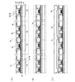
本発明を用いた薄膜集積回路装置及びその作製方法について、図1(A)〜図1(C)、図2(A)〜図2(C)、図3(A)、図3(B)、図12を用いて説明する。まず、基板41上に、剥離層43を形成する。ここでは、石英基板上に、500nmの膜厚のa−Si膜(非晶質シリコン膜)をスパッタ法により形成した。なお、基板としては、石英基板の他にも、ガラス基板、アルミナなど絶縁物質で形成される基板、シリコンウエハ基板、後工程の処理温度に耐え得る耐熱性を有するプラスチック基板等を用いることができる。この場合、酸化珪素(SiOx)、窒化珪素(SiNx)、窒素を含む酸化珪素(SiOxNy)(x>y)、酸素を含む窒化珪素(SiNxOy)(x>y)等、基板側から不純物などの拡散を防止するための下地絶縁膜を形成しておいてもよい。また、ステンレスなどの金属または半導体基板などの表面に酸化シリコンや窒化シリコンなどの絶縁膜を形成した基板なども用いることができる。
(Embodiment 1)
1A to 1C, FIG. 2A to FIG. 2C, FIG. 3A, and FIG. 3B about a thin film integrated circuit device and a manufacturing method thereof using the present invention. This will be described with reference to FIG. First, the
また、剥離層43としては、非晶質シリコンの他に、多結晶シリコン、単結晶シリコン、セミアモルファスシリコン(SAS、微結晶シリコンともいう。)等、シリコンを主成分とする層を用いることができる。これらの剥離層43は、スパッタ法の他にも、プラズマCVD法等によって形成しても良い。また、剥離層43は500nmよりも薄く形成しても良い。
In addition to the amorphous silicon, the
次に、剥離層43上に、下地膜44を形成する。ここでは、100nm(1000Å)の膜厚の酸化珪素膜をスパッタ法によって形成した。なお、下地膜44は、ClF3等のハロゲン化フッ素によるエッチングから、薄膜集積回路を保護する役割を有するものであり、この機能を有するものであれば、他の材料を用いてもよい。例えば、窒化珪素、窒素を含む酸化珪素、酸素を含む窒化珪素等を用いることができる。または、上記材料からなる膜を積層して下地膜44を形成しても良い。また、スパッタ法に限らず、プラズマCVD法等によって形成しても良い。
Next, a
次に、下地膜44上に薄膜集積回路42、例えば薄膜トランジスタ(TFT)、有機TFT、薄膜ダイオード等を形成する。図1(A)に示す薄膜集積回路42は、下地膜44上に、チャネル形成領域35、不純物領域36、ゲート絶縁膜37及びゲート電極38が形成されている。本実施の形態では、トップゲート構造としたが、ボトムゲート構造(逆スタガ構造)としてもよい。また、薄膜トランジスタの代わりに有機TFTや薄膜ダイオードを用いてもよい。これらの薄膜集積回路が薄膜集積回路装置のCPUやメモリ等を構成する。TFTを用いたCPUやメモリ等の薄膜集積回路の作製方法の具体例については、後述する。なお、薄膜集積回路装置は、図18等に示すように、電源回路、入出力回路、論理回路、CPU、メモリ等からなるが、ここでは、TFTを用いたCPU33と、メモリ34のみを図示した。
Next, a thin film integrated
次に、薄膜集積回路42を保護するために、第1の層間絶縁膜46を形成する。ここでは、窒化珪素膜をプラズマCVD法によって形成したが、これに限定されるものではない。さらに、第2の層間絶縁膜47を形成する。これは、薄膜集積回路を平坦化するものであり、ポリイミド、アクリル、ポリアミドや、シロキサン等の耐熱性有機樹脂を、スピンコート法、ディップ法、スプレー法、液滴吐出法等によって形成することができる。また、無機材料を用いてもよく、その際には、PSG(リンガラス)、BPSG(リンボロンガラス)、アルミナ膜等を用いることができる。
Next, in order to protect the thin film integrated
次に、レジストをマスクとしてコンタクトホールをエッチング開孔し、薄膜集積回路同士を接続する配線45及びアンテナ48を形成した。導電材料としては、Ag、Au、Al、Cu、Zn、Sn、Ni、Cr、Fe、Co若しくはTi、又はそれらを含む合金を用いることができるが、これらに限定されるものではない。また、配線とアンテナで材料が異なっていても良い。なお、配線45及びアンテナ48は、展性、延性に富む金属材料を有するように形成し、更に好ましくは膜厚を厚くして変形による応力に耐えるようにするのが望ましい。
Next, the contact hole was etched by using the resist as a mask, and the
また、配線及びアンテナの形成方法としては、スパッタ法によって全面成膜した後、レジストマスクを用いてパターニングを行ってもよいし、液滴吐出法によってノズルから選択的に形成しても良い。なお、ここでいう液滴吐出法には、インクジェット法のみならず、オフセット印刷法やスクリーン印刷等も含まれる。 As a method for forming the wiring and the antenna, after forming a film on the entire surface by a sputtering method, patterning may be performed using a resist mask, or selective formation from a nozzle may be performed by a droplet discharge method. Note that the droplet discharge method here includes not only an inkjet method but also an offset printing method and a screen printing.
また、薄膜集積回路装置を内蔵する商品が、導電材料を含む場合には、それと同様の導電材料を用いて、アンテナ又は配線を形成しても良い。例えば、硬貨の材料を用いて硬貨の内部にアンテナを形成することができる。この場合、例えば、10円玉に薄膜集積回路装置を埋め込む場合には、銅、亜鉛、スズの合金からなるアンテナを形成すると良い。 In the case where a product incorporating a thin film integrated circuit device contains a conductive material, an antenna or a wiring may be formed using the same conductive material. For example, an antenna can be formed inside a coin using a coin material. In this case, for example, when a thin film integrated circuit device is embedded in a 10-yen coin, an antenna made of an alloy of copper, zinc, and tin is preferably formed.
次に、アンテナ上に、保護膜49を形成する。保護膜49としては、DLC(ダイヤモンドライクカーボン)或いは窒化炭素(CN)等の炭素を有する膜、又は窒化珪素膜或いは酸素を含む窒化珪素膜等を用いることができる。あるいは、ポリイミド、アクリル、ポリアミドや、シロキサン等の耐熱性有機樹脂を用いることができる。また、無機材料を用いてもよく、その際には、PSG(リンガラス)、BPSG(リンボロンガラス)、アルミナ膜等を用いることができる。また、エポキシ樹脂を用いることもできる。なお、これらの絶縁膜を積層させて、保護膜49を形成しても良い。
Next, a
なお、ここでは、薄膜集積回路上に、第1の層間絶縁膜46、第2の層間絶縁膜47、保護膜49の3つの絶縁膜を形成したが、それらの材料は、互いに入れ替えて用いることができる。また、第1及び第2の層間絶縁膜46及び47を兼ねて、一層の層間絶縁膜としてもよい。いずれにしても、これらの絶縁膜に用いられる材料としては、後のClF3(三フッ化塩素)等のハロゲン化フッ素によるエッチングによって冒されず、かつ耐熱性がある材料を用いるのが望ましい(図1(A))。
Here, the three insulating films of the first
なお、層間絶縁膜46及び47や保護膜49としては、弾性の高い有機材料を用いるのが望ましい。これにより、変形時の応力は、有機材料を有する層間絶縁膜や保護膜に集中し、主にこれらの膜が変形するので、薄膜トランジスタへかかる応力が低減される。また変形が生じる場合に、最も応力が負荷される箇所(エッジ、角)が、半導体膜のエッジではなく下地膜のエッジとなるため、半導体膜のエッジや界面で生じる応力集中を抑えることができる。
As the
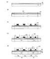
次に、薄膜集積回路装置50の境界領域に、ダイシングによって溝93を形成する(図1(B))。この際、ダイシング装置(ダイサー;dicer)を用いるブレードダイシング法を用いるのが一般的である。ブレード(blade)とは、ダイヤモンド砥粒を埋め込んだ砥石で、その幅は約30〜50μmであり、このブレードを高速回転させることにより、薄膜集積回路装置を分離する。また、ダイシングに必要なエリアをストリートと呼ぶが、この幅は、素子への損傷を考慮し、80〜150μmとしておくのが望ましい。
Next, a
なお、ダイシングの他にも、スクライビング又はマスクを利用したエッチング等によって行うことができる。スクライビングの場合には、ダイヤモンドスクライビング法とレーザースクライビング法等がある。また、エッチングの場合には、露光、現像工程によりマスクパターンを形成し、ドライエッチング、ウエットエッチング等により素子分離を行うことができる。ドライエッチングにおいては、大気圧プラズマ法を用いてもよい。 In addition to dicing, scribing or etching using a mask can be used. In the case of scribing, there are a diamond scribing method and a laser scribing method. In the case of etching, a mask pattern can be formed by exposure and development processes, and element isolation can be performed by dry etching, wet etching, or the like. In dry etching, an atmospheric pressure plasma method may be used.
なお、溝を形成する場合、溝の深さは、少なくとも剥離層の表面が露出する程度とすればよく、基板41が繰り返し利用できるように、基板に傷が付かないように上記ダイシング等を適宜制御するのが望ましい。
When forming the groove, the depth of the groove may be at least enough to expose the surface of the peeling layer, and the above dicing or the like may be appropriately performed so that the
次に、突起部58を有するジグ(支持基板)52を、仮接着剤51を介して、薄膜集積回路装置50毎に取り付ける。ここで、ジグ(治具)とは、剥離層を除去した後に薄膜集積回路装置がバラバラに分離しないように、一時的に薄膜集積回路装置を固定する役割を有する。ジグの形状としては、図1(C)のように、後にハロゲン化フッ素を含む気体又は液体の導入を容易にするために、突起部58を設けた櫛状の構造とするのが望ましいが、図4(C)のように平坦なジグを用いても構わない。突起部を有するジグ(治具、支持基板)を用いる場合には、基板をパターニングして用いればよい。また、ジグとしては、ハロゲン化フッ素によって冒されない酸化珪素を主成分とするガラス基板、石英基板、ステンレス(SUS)基板等を用いることができるが、ハロゲン化フッ素によって冒されない材料であれば、これらに限定されるものではない。また、ジグと薄膜集積回路との間には、仮接着するための接着剤が設けられている。
Next, a jig (support substrate) 52 having a
ここで、接着剤としては、UV光照射によって接着力(粘着力)が低下又は喪失する材料を用いることができる。ここでは、日東電工社製UV照射剥離テープを用いた。これ以外にも、例えば、前述した特開2001−30403、特許2992092、特開平6−299127に記載された、アクリル系粘着剤、合成ゴム系粘着剤、天然ゴム系粘着剤等を用いることができる。勿論、ジグを簡単に取り外すことができる材料であれば、これらに限定されるものではない。 Here, as the adhesive, a material whose adhesive strength (adhesive strength) is reduced or lost by UV light irradiation can be used. Here, a UV irradiation peeling tape manufactured by Nitto Denko Corporation was used. Other than this, for example, an acrylic pressure-sensitive adhesive, a synthetic rubber pressure-sensitive adhesive, a natural rubber pressure-sensitive adhesive and the like described in JP-A-2001-30403, JP-A-2992092, and JP-A-6-299127 described above can be used. . Of course, the material is not limited to these as long as the jig can be easily removed.
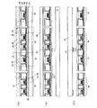
次に、溝93にハロゲン化フッ素ガスを導入することにより、剥離層43であるa−Si膜をエッチング除去した(図2(A))。ここで用いた減圧CVD装置(図12)は、反応空間であるベルジャー89内に、ClF3ガス等のハロゲン化フッ素ガス53が導入され、ガスが基板90に行き渡る仕組みになっている。また、ベルジャー89の外部にはヒーター91が設けられ、残余ガスは、排気管92から排出される。ここでは、図12に示すような減圧CVD装置を用い、ガス:ClF3、温度:350℃、流量:300sccm、気圧:6Torr、時間:3hの条件でa−Si膜のエッチング除去を行ったが、この条件に限定されるものではない。また、ClF3ガスに窒素を混ぜたガスを用いてもよい。両者の流量比は適宜設定することができる。
Next, by introducing a halogenated fluorine gas into the
ここで、ClF3等のハロゲン化フッ素は、シリコンを選択的にエッチングするという特性がある反面、酸化珪素(SiOx)、窒化珪素(SiNx)、窒素を含む酸化珪素(SiOxNy(x>y))、酸素を含む窒化珪素(SiNxOy(x>y))はほとんどエッチングされない。したがって、時間の経過とともに剥離層43はエッチングされ、最終的に基板41を剥離することができる(図2(B))。一方、酸化珪素、窒化珪素、窒素を含む酸化珪素、酸素を含む窒化珪素等や、耐熱性樹脂からなる下地膜や、層間絶縁膜、保護膜はほとんどエッチングされないため、薄膜集積回路への損傷を防止することができる。なお、剥離した基板41は勿論再利用することができ、コスト削減に繋がる。
Here, fluorine halide such as ClF 3 has a characteristic of selectively etching silicon, but silicon oxide (SiOx), silicon nitride (SiNx), and silicon oxide containing nitrogen (SiOxNy (x> y)). Silicon nitride containing oxygen (SiNxOy (x> y)) is hardly etched. Therefore, the
次に、UV光照射を行うことにより、仮接着剤51の粘着力を低下又は喪失させ、ジグ52と、薄膜集積回路装置とを分離することにより、薄膜集積回路装置を大量に作製することができる。なお、ジグは、コスト削減のため、再利用するのが望ましい。
Next, by performing UV light irradiation, the adhesive strength of the
上記方法によって作製された薄膜集積回路装置50は、小型真空ピンセット13等により、搬送し、所望の製品に備え付けることができる。図3(A)、図3(B)は、商品10に貼付されるIDラベル15の作製方法を示したものである。ラベル11に薄膜集積回路装置50を小型真空ピンセット13により貼り付け、接着剤14で封止し、IDラベル15が完成する。さらに、商品10にIDラベル15を付して、リーダ/ライタ等によって情報を認識、更新、管理しうる商品が完成する。
The thin film integrated
(実施形態2)
本実施形態では、溝93を形成するにあたり、ドライエッチング法を用いる場合について、図4(A)〜(C)を用いて説明する。実施形態1の記載に基づいて、図1(A)に示す保護膜49形成までを行う。その後、現像、露光工程を経て、基板上にレジスト54を形成し、レジスト54をマスクとして、ドライエッチングにより溝93を形成し、素子分離を行う(図4(A))。ここでは、プラズマエッチングを採用し、エッチング用ガスとしては、Cl2、BCl3、SiCl4もしくはCCl4などを代表とする塩素系ガス、CF4、SF6、NF3、CHF3などを代表とするフッ素系ガス、あるいはO2を用いたが、これらに限定されるものではない。なお、該エッチングは、大気圧プラズマを利用して行うこともできる。この際、エッチングガスとしては、CF4とO2の混合ガスを用いるのがよい。また、ガス種の異なるエッチングを複数回行うことによって溝93を形成しても良い。
(Embodiment 2)
In the present embodiment, a case where a dry etching method is used to form the
次に、仮接着剤51を介して、ジグ55を薄膜集積回路装置50に取り付け、ClF3等のハロゲン化フッ素によって、剥離層43を除去し、最終的に基板41を剥離した(図4(B))。剥離層43除去の具体的な方法は、実施形態1と同様である。なお、ジグ55として、ここでは、突起部を特に設けていない基板を用いたが、勿論、突起部を有した基板を用いてもよい。
Next, the
次に、UV光照射を行うことにより、仮接着剤51の粘着力を低下又は喪失させ、ジグ55と、薄膜集積回路装置50とを分離する(図4(C))。これにより、薄膜集積回路装置50を大量に作製することができる。上記方法によって作製された薄膜集積回路装置50は、小型真空ピンセット等により、搬送し、所望の製品に備え付けることができる。
Next, by performing UV light irradiation, the adhesive force of the
(実施形態3)
本実施形態では、ダイシング等によって溝93を形成する際に、基板41に傷が付いた場合、その基板を再利用する場合について図5(A)、図5(B)、図6(A)〜図6(C)を用いて説明する。
(Embodiment 3)
In this embodiment, when the
まず、図5(A)に示すように、使用済み基板56上に平坦化膜57を形成する。平坦化膜としては、ポリイミド、アクリル、ポリアミドや、シロキサン等の耐熱性樹脂を、スピンコート法、ディップ法、スプレー法、液滴吐出法等によって形成することができる。後工程の熱処理を考慮すれば、シロキサン等の耐熱性樹脂を用いることが望ましい。また、無機材料を用いてもよく、その際には、PSG(リンガラス)、BPSG(リンボロンガラス)、アルミナ膜等を用いることができる。その後、実施形態1又は2に基づいて薄膜集積回路を作製、分離して所望の製品に備え付けることができる。
First, as shown in FIG. 5A, a
他の方法として、図6(A)〜図6(C)に示すように、CMP(機械的化学的研磨)法、プレス法、エッチバック法等により、基板表面を平坦化する方法がある。CMP法(図6(A))の場合には、使用済み基板56の傷が微細である場合に特に有効である。CMP法は、研磨用パッド308内にスラリー(307)と呼ばれる研磨溶剤を供給し、ウエハキャリア306の回転とプラテンと呼ばれる回転台の回転による加圧と、研磨用パッドの研磨によって平坦化を行うものである。基板は、ガラス基板のように絶縁体であるので、スラリー307としては、アルカリ性のコロイド状シリカを混ぜたものが主に用いられる。また、プレス法(図6(B))の場合には、ヒーター301等の加熱機構を備えた装置300によってプレスを行うのがよい。また、エッチバック法(図6(C))では、絶縁膜309を平坦に形成した後に、エッチングを行って、平坦化するものである。その後、実施形態1又は2に基づいて薄膜集積回路装置を作製、分離して所望の製品に備え付けることができる。
As another method, as shown in FIGS. 6A to 6C, there is a method of planarizing the substrate surface by a CMP (mechanical chemical polishing) method, a press method, an etch back method, or the like. In the case of the CMP method (FIG. 6A), it is particularly effective when the scratches on the used
(実施形態4)
上記実施形態では、薄膜集積回路の作製工程において、アンテナを形成したが、本実施形態では、基板上に作製されたアンテナと、複数の薄膜集積回路からなる集積回路を別々に作製し、その後両者を接続する方法について、図7(A)〜図7(C)、図8(A)〜図8(E)、図9(A)、図9(B)、図10(A)、図10(B)、図18を用いて説明する。
(Embodiment 4)
In the above embodiment, the antenna is formed in the manufacturing process of the thin film integrated circuit. However, in this embodiment, the antenna manufactured on the substrate and the integrated circuit including a plurality of thin film integrated circuits are separately manufactured, and then both 7A to FIG. 7C, FIG. 8A to FIG. 8E, FIG. 9A, FIG. 9B, FIG. 10A, and FIG. (B) will be described with reference to FIG.
第1の方法は、図7(A)に示すように、折り曲げ可能なフレキシブル基板69上に、アンテナ68を形成し、別途形成した集積回路25を図7(B)に示すアンテナの接続部99と接続した後に、フレキシブル基板69を図7(C)に示すように半分に折りたたみ、封止して薄膜集積回路装置を作製するというものである。ここで、アンテナ68は、スパッタ法等によって形成した後にパターニング形成しても良いし、液滴吐出法を用い、導電材料を含む組成物を選択的に吐出した後に、該組成物を乾燥、焼成することにより形成しても良い。
In the first method, as shown in FIG. 7A, an
なお、アンテナを形成した後に、図6(A)〜図6(C)に示す、CMP法、プレス法、エッチバック法等により、平坦性を向上させても良い。CMP法の場合には、アンテナは導電性材料からなるので、スラリーとしては、酸性溶液にアルミナの微粉末を混ぜたものを用いるのがよい。また、プレス法の場合には、ヒーター301等の加熱機構を備えた装置によってプレスを行うのがよい。また、エッチバック法では、絶縁膜309を平坦に形成した後に、エッチングを行って、平坦化するものである。なお、これらの平坦化処理工程は、薄膜集積回路の作製工程において用いることもできる。
Note that after the antenna is formed, planarity may be improved by a CMP method, a press method, an etch back method, or the like shown in FIGS. In the case of the CMP method, since the antenna is made of a conductive material, it is preferable to use a slurry obtained by mixing a fine powder of alumina in an acidic solution. In the case of the pressing method, the pressing is preferably performed by an apparatus having a heating mechanism such as a
アンテナには、アンテナ同士を接続する接続部98や、アンテナと集積回路を接続する接続部99を、アンテナ形成時に形成しておいても良い。また、集積回路との接続部99は、アンテナを形成した後に、アンテナの一部を切断することによって形成しても良い。なお、集積回路とアンテナとの接続は、異方性導電膜や、公知のボンディング法等を用いて行うことができる。また、アンテナの形状は、折り畳んだときに対称でコイル状であれば、図7(A)〜図7(C)に示す形状に限定されない。
The antenna may be formed with a
アンテナ基板に挟まれる集積回路25は、図18に示すように、電源回路26、入出力回路27、論理回路28、メモリ29、CPU30等に、リーダ/ライタ136との電波のやりとりを行うアンテナ回路が接続された構成を有している。
As shown in FIG. 18, the
なお、図8(A)〜図8(E)は、図7(C)のX−Y断面から見たアンテナ基板折り畳みの状態を示した図である。ここでは、アンテナ20をパターニング形成する際に用いたレジスト23をアッシング等によって除去してしまわずに、残存させた(図8(A))。さらに、平坦化膜60をスピンコート法、ディップ法、スプレー法、液滴吐出法等によって形成し、平坦化を行った(図8(B))。さらに、集積回路25(ICチップ)との接続部を確保するために、レジスト61をマスクとして、エッチング又はアッシングを行い、コンタクト部62を形成した(図8(C))。さらに、異方性導電膜63を介して集積回路25を形成し、シール剤64を介して、アンテナが形成されたフレキシブル基板19を折り畳み(図8(D))、薄膜集積回路装置66を完成させた(図8(E))。この際、対向するアンテナ同士の間に配線等を設けてアンテナ同士を接続しても良い。ここで、レジスト23や平坦化膜60は、基板を折り畳んだ際に、アンテナや集積回路を保護するクッションの役割を果たす。なお、レジスト23や平坦化膜60は、一方又は両方を省略することもできる。
FIGS. 8A to 8E are views showing the folded state of the antenna substrate viewed from the XY cross section of FIG. 7C. Here, the resist 23 used for patterning the
第2の方法は、図9(A)、図9(B)に示すように、基板69上にアンテナ68を複数形成しておき、基板69をダイシング等によって切り出し、アンテナ基板の間に集積回路25を挟む方法である。ここで、接続部21は、アンテナ同士を接続するために用いてもよいし、集積回路とアンテナとを接続するのに用いてもよい。また、接続部21は、アンテナの他の箇所に形成しても良い。なお、基板同士を貼り合わせる際に、アライメントマーカーを設ける必要があるが、該接続部21をマーカーとしても良い。
In the second method, as shown in FIGS. 9A and 9B, a plurality of
第3の方法は、図10(A)、図10(B)に示すように、二方が閉じられた食品を包装するラップ状のフレキシブル基板70や(図10(A))、三方が閉じられた封筒状のフレキシブル基板74に(図10(B))、アンテナ71を両面に形成しておき、その間に集積回路25(ICチップ)を挿入し、接着剤73で封止するという方法である。接続部21は開孔されており、アンテナ同士、又はアンテナと集積回路が接続することができる。ICチップは小型真空ピンセット等で設置すればよい。なお、アンテナは、これらの基板の内側に形成しておいても良い。
As shown in FIGS. 10 (A) and 10 (B), the third method is a wrap-shaped
以上、本実施形態で述べた薄膜集積回路装置の作製方法は、特に、アンテナ基板と、集積回路(ICチップ)とを別々の製造者が作製し、中間生成品(部品)として流通させる場合に適した方法である。 As described above, the manufacturing method of the thin film integrated circuit device described in this embodiment is particularly when the antenna substrate and the integrated circuit (IC chip) are manufactured by different manufacturers and distributed as intermediate products (components). It is a suitable method.
(実施形態5)
本実施形態では、図11(A)〜図11(C)を参照して、素子基板75に仮接着したジグ76を取り外さずに、直接、商品84等に接着する方法について説明する。まず、実施形態1〜3に基づいて、素子基板75を形成し、仮接着剤81を介してジグ76を取り付ける。ジグ76としては、図11(A)、図11(B)に示すように、突起部77を有するものを用いた。仮接着剤としては、ここでは、UV光照射によって粘着力が低下又は喪失する材料を用いる。また、素子への損傷を防ぐために、有機材料又は無機材料からなる層間膜79を設けている。そして、ClF3等のハロゲン化フッ素によるエッチングにより、素子分離を行う。
(Embodiment 5)
In the present embodiment, a method of directly bonding to the
次に、ジグ76に素子が仮接着された状態で搬送し、IDカード等の商品84が設置されたステージとのアライメントを行う。この際、図11(A)に示すように、ジグや、ステージに設けられたアライメントマーカー78、82を利用することもできるし、図示しないが、商品84に形成されたマーカーを利用することもできる。商品84内の薄膜集積回路装置が形成される部分には、予め接着剤85が形成されており、ジグを制御することにより、所望の素子を商品の所望の箇所に貼り付ける(図11(A))。
Next, the device is transported in a state where the elements are temporarily bonded to the
次に、商品84に貼り付けたい素子に、マスクを介してUV光86を選択的に照射し、仮接着剤81の粘着力を低下又は喪失させることにより、ジグと素子とを分離する(図11(B))。これにより、所望の素子(集積回路87)を商品の所望の箇所に形成することができる。素子形成後、カバー88等により、素子部をカバーする(図11(C))。なお、ここでは、商品84の内部にアンテナ83が形成された場合を示したが、素子部にアンテナを形成しておいても良い。
Next, the element desired to be attached to the
本実施形態に示した本発明を用いることにより、ClF3等のハロゲン化フッ素によるエッチングにより素子分離を行った際、素子がバラバラに分離することなく、所望の素子を所望の箇所に形成することができる。 By using the present invention shown in this embodiment, when elements are separated by etching with a halogenated fluorine such as ClF 3 , a desired element is formed at a desired position without being separated. Can do.
本実施例では、図13(A)〜図13(E)、図14(A)〜図14(E)を参照して、薄膜集積回路装置の集積回路部の具体的な作製方法について説明する。ここでは、簡単のため、nチャネル型TFTとpチャネル型TFTを用いたCPUとメモリの作製方法について説明する。 In this embodiment, a specific method for manufacturing an integrated circuit portion of a thin film integrated circuit device will be described with reference to FIGS. 13A to 13E and FIGS. 14A to 14E. . Here, for simplicity, a method for manufacturing a CPU and a memory using an n-channel TFT and a p-channel TFT will be described.
まず、基板41上に、剥離層43と、下地膜44を形成する(図13(A))。これらの材料や作製方法は、実施形態1〜実施形態5に述べたものを採用することができる。
First, the
次に、下地膜44上に、島状半導体膜100を形成する。島状半導体膜100は、アモルファス半導体、結晶性半導体、又はセミアモルファス半導体で形成する。いずれも、シリコン、シリコン・ゲルマニウム(SiGe)等を主成分とする半導体膜を用いることができる。
Next, the island-shaped
本実施例では、70nmの膜厚のアモルファスシリコンを形成し、さらにその表面を、シリコンの結晶化を促進する触媒元素、例えばニッケルを含む溶液で処理した後、500〜750℃の熱結晶化工程によって結晶性シリコン膜を得、さらにレーザー結晶化を行って結晶性の改善を施した。また、成膜方法としては、プラズマCVD法、スパッタ法、LPCVD法などを用いても良いし、結晶化方法としては、レーザー結晶化法、熱結晶化法、他の触媒元素(Fe,Ru,Rh,Pd,Os,Ir,Pt,Cu,Au等)を用いた熱結晶化、あるいはそれらを交互に複数回行っても良い。 In this example, amorphous silicon having a film thickness of 70 nm is formed, and the surface thereof is further treated with a solution containing a catalytic element that promotes crystallization of silicon, such as nickel, and then a thermal crystallization process at 500 to 750 ° C. Thus, a crystalline silicon film was obtained, and further crystallized by laser crystallization. Further, as a film formation method, a plasma CVD method, a sputtering method, an LPCVD method, or the like may be used. As a crystallization method, a laser crystallization method, a thermal crystallization method, or other catalytic elements (Fe, Ru, Rh, Pd, Os, Ir, Pt, Cu, Au, etc.) or they may be alternately performed a plurality of times.
また、非晶質構造を有する半導体膜の結晶化処理としては、連続発振のレーザーを用いても良く、結晶化に際し大粒径の結晶を得るためには、連続発振が可能な固体レーザーを用い、基本波の第2高調波〜第4高調波を適用するのが好ましい。代表的には、Nd:YVO4レーザー(基本波1064nm)の第2高調波(532nm)や第3高調波(355nm)を適用すればよい。連続発振のレーザーを用いる場合には、出力10Wの連続発振のYVO4レーザーから射出されたレーザー光を非線形光学素子により高調波に変換する。また、共振器の中にYVO4結晶と非線形光学素子を入れて、高調波を射出する方法もある。そして、好ましくは光学系により照射面にて矩形状または楕円形状のレーザー光に成形して、被処理体に照射する。このときのエネルギー密度は0.01〜100MW/cm2程度、好ましくは0.1〜10MW/cm2、が必要である。そして、10〜2000cm/s程度の速度でレーザー光に対して相対的に半導体膜を移動させて照射すればよい。 In addition, a continuous wave laser may be used for the crystallization treatment of the semiconductor film having an amorphous structure, and a solid laser capable of continuous oscillation is used in order to obtain a crystal having a large particle size upon crystallization. It is preferable to apply the second to fourth harmonics of the fundamental wave. Typically, a second harmonic (532 nm) or a third harmonic (355 nm) of an Nd: YVO 4 laser (fundamental wave 1064 nm) may be applied. In the case of using a continuous wave laser, laser light emitted from a continuous wave YVO 4 laser having an output of 10 W is converted into a harmonic by a non-linear optical element. There is also a method of emitting harmonics by putting a YVO 4 crystal and a nonlinear optical element in a resonator. Preferably, the laser beam is shaped into a rectangular or elliptical shape on the irradiation surface by an optical system, and the object to be processed is irradiated. At this time, the energy density of 0.01 to 100 MW / cm 2 mm, preferably required 0.1 to 10 MW / cm 2, it is. Then, irradiation may be performed by moving the semiconductor film relative to the laser light at a speed of about 10 to 2000 cm / s.
上記の方法によって結晶性シリコン膜を得た後、半導体膜上に酸化シリコン膜を介して、触媒元素をゲッタリングするためのアモルファスシリコン膜を成膜し、500〜750℃の熱処理によってゲッタリング処理を行った。さらに、TFT素子としての閾値を制御するために、結晶性シリコン膜に対し、1013/cm2オーダーのドーズ量のホウ素イオンを注入した。その後、レジストをマスクとしてエッチングを行うことにより、島状半導体膜100を形成した。
After obtaining the crystalline silicon film by the above method, an amorphous silicon film for gettering the catalytic element is formed on the semiconductor film via the silicon oxide film, and gettering treatment is performed by heat treatment at 500 to 750 ° C. Went. Furthermore, in order to control the threshold value as the TFT element, boron ions having a dose of the order of 10 13 / cm 2 were implanted into the crystalline silicon film. Then, the island-shaped
なお、結晶性半導体膜を形成するにあたっては、ジシラン(Si2H6)とフッ化ゲルマニウム(GeF4)の原料ガスとして、LPCVD(減圧CVD)法によって、多結晶半導体膜を直接形成することによっても、結晶性半導体膜を得ることができる。ガス流量比は、Si2H6/GeF4=20/0.9、成膜温度は400〜500℃、キャリアガスとしてHe又はArを用いたが、これに限定されるものではない。 In forming a crystalline semiconductor film, a polycrystalline semiconductor film is directly formed by LPCVD (low pressure CVD) as a source gas of disilane (Si 2 H 6 ) and germanium fluoride (GeF 4 ). Also, a crystalline semiconductor film can be obtained. The gas flow ratio is Si 2 H 6 / GeF 4 = 20 / 0.9, the film forming temperature is 400 to 500 ° C., and He or Ar is used as the carrier gas, but the present invention is not limited to this.
次に、島状半導体膜100上にゲート絶縁膜102を形成する(図13(B))。ゲート絶縁膜102はプラズマCVD法又はスパッタリング法などの薄膜形成法を用い、窒化珪素、酸化珪素、酸素を含む窒化珪素又は窒素を含む酸化珪素を含む膜を、単層で、又は積層させて形成することが好ましい。積層する場合には、例えば、基板側から酸化珪素膜、窒化珪素膜、酸化珪素膜の3層構造とするのがよい。
Next, the
次に、ゲート電極103を形成する(図13(C))。本実施例では、30nmの膜厚のTaN(窒化タンタル)と、370nmの膜厚のW(タングステン)をスパッタ法により積層形成した後に、レジスト104をマスクとしてエッチングを行うことにより、ゲート電極103を形成した。ここで、レジストマスクの代わりに、酸化珪素等のマスクを用いてもよい。この場合、酸化珪素、窒素を含む酸化珪素等のマスク(ハードマスクと呼ばれる。)をパターニング形成工程が加わるが、エッチング時におけるマスクの膜減りがレジストよりも少ないため、所望の幅のゲート電極103を形成することができる。勿論、ゲート電極103の材料、構造、作製方法は、これに限定されるものではなく、適宜選択することができる。例えば、レジスト104を用いずに、液滴吐出法を用いて選択的にゲート電極103を形成しても良い。 Next, the gate electrode 103 is formed (FIG. 13C). In this embodiment, TaN (tantalum nitride) with a thickness of 30 nm and W (tungsten) with a thickness of 370 nm are stacked by sputtering, and then etched using the resist 104 as a mask, whereby the gate electrode 103 is formed. Formed. Here, a mask made of silicon oxide or the like may be used instead of the resist mask. In this case, a mask (referred to as a hard mask) made of silicon oxide, silicon oxide containing nitrogen, or the like is added to the patterning step. However, the thickness of the gate electrode 103 having a desired width is less than that of the resist during etching. Can be formed. Needless to say, the material, structure, and manufacturing method of the gate electrode 103 are not limited to these, and can be selected as appropriate. For example, the gate electrode 103 may be selectively formed using a droplet discharge method without using the resist 104.
なお、ゲート電極103を形成するための導電材料としては、導電膜の機能に応じて種々の材料を選択することができるが、代表的なものとして、銀(Ag)、銅(Cu)、金(Au)、ニッケル(Ni)、白金(Pt)、クロム(Cr)、スズ(Sn)、パラジウム(Pd)、イリジウム(Ir)、ロジウム(Rh)、ルテニウム(Ru)、レニウム(Re)、タングステン(W)、アルミニウム(Al)、タンタル(Ta)、インジウム(In)、テルル(Te)、モリブデン(Mo)、カドミウム(Cd)、亜鉛(Zn)、鉄(Fe)、チタン(Ti)、シリコン(Si)、ゲルマニウム(Ge)、ジルコニウム(Zr)、バリウム(Ba)、アンチモン鉛、酸化スズ・アンチモン、フッ素ドープ酸化亜鉛、炭素、グラファイト、グラッシーカーボン、リチウム、ベリリウム、ナトリウム、マグネシウム、カリウム、カルシウム、スカンジウム、マンガン、ジルコニウム、ガリウム、ニオブ、ナトリウム−カリウム合金、マグネシウム/銅混合物、マグネシウム/銀混合物、マグネシウム/アルミニウム混合物、マグネシウム/インジウム混合物、アルミニウム/酸化アルミニウム混合物、リチウム/アルミニウム混合物等、ハロゲン化銀の微粒子等、又は分散性ナノ粒子、あるいは、透明導電膜として用いられる酸化インジウムスズ(ITO:Indium Tin Oxide)、酸化珪素を含む酸化インジウムスズ(酸化珪素を含むインジウム錫酸化物ともいう、以下、本明細書では「ITSO:indium tin silicon oxide」という。)、酸化亜鉛(ZnO:Zinc Oxide)、ガリウムを添加した酸化亜鉛(GZO)、酸化インジウムに2〜20%の酸化亜鉛を混合した酸化インジウム亜鉛(IZO:Indium Zinc Oxide)、有機インジウム、有機スズ、窒化チタン等を適宜採用することができる。 Note that a variety of materials can be selected as a conductive material for forming the gate electrode 103 depending on the function of the conductive film. Typical examples include silver (Ag), copper (Cu), and gold. (Au), nickel (Ni), platinum (Pt), chromium (Cr), tin (Sn), palladium (Pd), iridium (Ir), rhodium (Rh), ruthenium (Ru), rhenium (Re), tungsten (W), aluminum (Al), tantalum (Ta), indium (In), tellurium (Te), molybdenum (Mo), cadmium (Cd), zinc (Zn), iron (Fe), titanium (Ti), silicon (Si), germanium (Ge), zirconium (Zr), barium (Ba), antimony lead, tin oxide / antimony, fluorine-doped zinc oxide, carbon, graphite, glass Sea carbon, lithium, beryllium, sodium, magnesium, potassium, calcium, scandium, manganese, zirconium, gallium, niobium, sodium-potassium alloy, magnesium / copper mixture, magnesium / silver mixture, magnesium / aluminum mixture, magnesium / indium mixture, Aluminum / aluminum oxide mixture, lithium / aluminum mixture, etc., silver halide fine particles, or dispersible nanoparticles, or indium tin oxide (ITO) used as a transparent conductive film, indium oxide containing silicon oxide Tin (also referred to as indium tin oxide containing silicon oxide, hereinafter referred to as “ITSO: indium tin silicon oxide”), zinc oxide (ZnO: Zinc Oxide), zinc oxide added with gallium ( GZO), indium zinc oxide (IZO) in which 2 to 20% zinc oxide is mixed with indium oxide, organic indium, organic tin, titanium nitride, or the like can be appropriately employed.
なお、ゲート電極103をエッチング形成する際のエッチングガスとしては、CF4、Cl2及びO2の混合ガスやCl2ガスを用いたが、これに限定されるものではない。 Note that a mixed gas of CF 4 , Cl 2 and O 2 or a Cl 2 gas is used as an etching gas for forming the gate electrode 103 by etching, but the present invention is not limited to this.
次に、pチャネル型TFT109,111となる部分をレジスト118で覆い、ゲート電極103をマスクとして、nチャネル型TFT108、110の島状半導体膜に、第1の不純物導入工程としてn型を付与する不純物元素119(代表的にはP(リン)又はAs(砒素))を低濃度に導入する(図13(D))。第1の不純物導入の条件は、ドーズ量:1×10¹³〜6×10¹³/cm2、加速電圧:50〜70keVとしたが、これに限定されるものではない。この第1の不純物導入によって、ゲート絶縁膜102を介してスルードープがなされ、一対の低濃度不純物領域120が形成される。なお、第1の不純物導入は、pチャネル型TFT領域をレジストで覆わずに、全面に行っても良い。
Next, the portions to be the p-
次に、レジスト118をアッシング等により除去した後、nチャネル型TFT領域を覆うレジスト121を新たに形成し、ゲート電極をマスクとして、pチャネル型TFT109、111の島状半導体膜に、第2の不純物導入工程としてp型を付与する不純物元素122(代表的にはB(ホウ素))を高濃度に導入する(図13(E))。第2の不純物導入の条件は、ドーズ量:1×10¹⁶〜3×10¹⁶/cm2、加速電圧:20〜40keVとして行う。この第2の不純物導入によって、ゲート絶縁膜102を介してスルードープがなされ、一対のp型の高濃度不純物領域123が形成される。
Next, after removing the resist 118 by ashing or the like, a resist 121 that covers the n-channel TFT region is newly formed, and the second semiconductor film is formed on the island-shaped semiconductor films of the p-
次に、レジスト121をアッシング等により除去した後、基板表面に、絶縁膜105を形成した(図14(A))。ここでは、膜厚100nmの窒素を含む酸化珪素(SiON)膜と、膜厚200nmの酸化膜の2層構造とした。ここでは、SiON膜は、プラズマCVD法で形成し、酸化膜としては、酸化珪素膜を減圧CVD法で形成した。その後、図示しないが、基板のTFTが形成された側をレジストで覆い、基板の裏面に形成された絶縁膜をエッチング除去した(裏面処理)。
Next, after removing the resist 121 by ashing or the like, an insulating
次に、レジストを残したまま、エッチバック法により、レジスト及び絶縁膜105をエッチング除去し、サイドウォール(側壁)106を自己整合的(セルフアライン)に形成した(図14(B))。エッチングガスとしては、CHF3とHeの混合ガスを用いた。なお、サイドウォールを形成する工程は、これらに限定されるものではない。
Next, with the resist remaining, the resist and the insulating
次に、pチャネル型TFT領域を覆うレジスト124を新たに形成し、ゲート電極103及びサイドウォール106をマスクとして、第3の不純物導入工程として、n型を付与する不純物元素125(代表的にはP又はAs)を高濃度に導入する(図14(C))。第3の不純物導入の条件は、ドーズ量:1×10¹³〜5×10¹⁵/cm2、加速電圧:60〜100keVとして行う。この第3の不純物導入によって、ゲート絶縁膜102を介してスルードープがなされ、一対のn型の高濃度不純物領域126が形成される。
Next, a resist 124 that covers the p-channel TFT region is newly formed, and an
なお、図示しないが、レジスト124をアッシング等により除去した後、不純物領域の熱活性化を行っても良い。例えば、50nmの窒素を含む酸化珪素膜を成膜した後、550℃、4時間、窒素雰囲気下において、加熱処理を行えばよい。また、水素を含む窒化珪素膜(SiNx膜)を、100nmの膜厚に形成した後、410℃、1時間、窒素雰囲気下において、加熱処理を行うことにより、結晶性半導体膜の欠陥を改善することができる。これは、例えば、結晶性シリコン中に存在するダングリングボンドを終端させるものであり、水素化処理工程などと呼ばれる。さらに、この後、TFTを保護するキャップ絶縁膜として、膜厚600nmのSiON膜を形成する。なお、水素化処理工程は、該SiON膜形成後に行っても良い。この場合、窒化珪素膜の上に窒素を含む酸化珪素膜を順次成膜した絶縁膜は連続成膜することができる。このように、TFT上には、基板側から、窒素を含む酸化珪素膜、窒化珪素膜、窒素を含む酸化珪素膜を順次積層した3層の絶縁膜が形成されることになるが、その構造や材料はこれらに限定されるものではない。また、これらの絶縁膜は、TFTを保護する機能をも有しているため、できるだけ形成しておくのが望ましい。 Although not shown, the impurity region may be thermally activated after the resist 124 is removed by ashing or the like. For example, after a silicon oxide film containing nitrogen with a thickness of 50 nm is formed, heat treatment may be performed in a nitrogen atmosphere at 550 ° C. for 4 hours. Further, after a silicon nitride film containing hydrogen (SiNx film) is formed to a thickness of 100 nm, heat treatment is performed in a nitrogen atmosphere at 410 ° C. for 1 hour to improve defects in the crystalline semiconductor film. be able to. This terminates dangling bonds existing in, for example, crystalline silicon, and is called a hydrogenation process. Thereafter, a SiON film having a film thickness of 600 nm is formed as a cap insulating film for protecting the TFT. Note that the hydrogenation process may be performed after the formation of the SiON film. In this case, the insulating film in which the silicon oxide film containing nitrogen is sequentially formed on the silicon nitride film can be continuously formed. Thus, on the TFT, a three-layer insulating film in which a silicon oxide film containing nitrogen, a silicon nitride film, and a silicon oxide film containing nitrogen are sequentially laminated is formed from the substrate side. The materials are not limited to these. In addition, these insulating films have a function of protecting the TFT, so that it is desirable to form them as much as possible.
次に、TFT上に、層間絶縁膜107を形成する。層間絶縁膜107として、ポリイミド、アクリル、ポリアミドや、シロキサン等の耐熱性有機樹脂を用いることができる。形成方法としては、その材料に応じて、スピンコート、ディップ、スプレー塗布、液滴吐出法(インクジェット法、スクリーン印刷、オフセット印刷等)、ドクターナイフ、ロールコーター、カーテンコーター、ナイフコーター等を採用することができる。また、無機材料を用いてもよく、その際には、PSG(リンガラス)、BPSG(リンボロンガラス)、アルミナ膜等を用いることができる。なお、これらの絶縁膜を積層させて、層間絶縁膜107を形成しても良い。
Next, an
次に、レジストを形成した後、エッチングによりコンタクトホールを開孔し、配線128及びアンテナ48を形成する(図14(D))。コンタクトホール開孔時のエッチングに用いられるガスは、CHF3とHeの混合ガスを用いたが、これに限定されるものではない。
Next, after forming a resist, a contact hole is formed by etching, so that a
また、配線128とアンテナ48は同一材料を用いて同時に形成しても良いし、別々に形成しても良い。ここでは、TFTと接続される配線128は、基板側から、Ti、TiN、Al−Si、TiN、Tiを順次積層した5層構造とし、スパッタ法によって形成した後、パターニング形成した。
Further, the
なお、Al層において、Siを混入させることにより、配線パターニング時のレジストベークにおけるヒロックの発生を防止することができる。また、Siの代わりに、0.5%程度のCuを混入させても良い。また、TiやTiNでAl−Si層をサンドイッチすることにより、耐ヒロック性がさらに向上する。なお、パターニング時には、窒素を含む酸化珪素(SiON)等からなる上記ハードマスクを用いるのが望ましい。なお、配線の材料や、形成方法はこれらに限定されるものではなく、前述したゲート電極に用いられる材料を採用しても良い。また、アンテナ48を形成する際には、上記実施の形態に示した、種々の材料、方法を用いることができる。配線とアンテナは、同時に形成しても良いし、一方を先に形成した後に、他方が乗り上げるように形成しても良い。
In addition, by mixing Si in the Al layer, generation of hillocks in resist baking during wiring patterning can be prevented. Further, instead of Si, about 0.5% Cu may be mixed. Further, the hillock resistance is further improved by sandwiching the Al—Si layer with Ti or TiN. In patterning, it is desirable to use the hard mask made of silicon oxide containing silicon (SiON) or the like. Note that the wiring material and the formation method are not limited to these, and the material used for the gate electrode described above may be employed. Further, when forming the
次に、配線及びアンテナ上に、保護膜49を形成し、CPU33及びメモリ34が完成する(図14(E))。保護膜49としては、DLC(ダイヤモンドライクカーボン)或いは窒化炭素(CN)等の炭素を有する膜、又は窒化珪素膜或いは酸素を含む窒化珪素膜等を用いることができる。形成方法としては、プラズマCVD法や、大気圧プラズマ等を用いることができる。
Next, a
あるいは、ポリイミド、アクリル、ポリアミド、レジスト又はベンゾシクロブテン等の感光性又は非感光性の有機材料や、シロキサン等の耐熱性有機樹脂、を用いることができる。形成方法としては、その材料に応じて、スピンコート、ディップ、スプレー塗布、液滴吐出法(インクジェット法、スクリーン印刷、オフセット印刷等)、ドクターナイフ、ロールコーター、カーテンコーター、ナイフコーター等を採用することができる。あるいは、塗布法により得られるSOG膜(例えば、アルキル基を含むSiOx膜)を用いることもできる。また、無機材料を用いてもよく、その際には、酸化珪素、窒化珪素、窒素を含む酸化珪素、酸素を含む窒化珪素、PSG(リンガラス)、BPSG(リンボロンガラス)、アルミナ膜等を用いることができる。なお、これらの絶縁膜を積層させて、保護膜49を形成しても良い。
Alternatively, a photosensitive or non-photosensitive organic material such as polyimide, acrylic, polyamide, resist, or benzocyclobutene, or a heat-resistant organic resin such as siloxane can be used. Depending on the material, spin coating, dipping, spray coating, droplet discharge methods (inkjet method, screen printing, offset printing, etc.), doctor knife, roll coater, curtain coater, knife coater, etc. are adopted as the forming method. be able to. Alternatively, an SOG film obtained by a coating method (for example, an SiOx film containing an alkyl group) can also be used. In addition, an inorganic material may be used. In that case, silicon oxide, silicon nitride, silicon oxide containing nitrogen, silicon nitride containing oxygen, PSG (phosphorus glass), BPSG (phosphorus boron glass), an alumina film, or the like is used. Can be used. Note that the
その後、本実施例によって作製された複数のTFTは、上記実施の形態に示す要領でICチップ毎に分離され、商品等に組み込むことができる。なお、本実施例では、トップゲート構造としたが、ボトムゲート構造(逆スタガ構造)としてもよい。 After that, the plurality of TFTs manufactured according to this example can be separated for each IC chip in the manner described in the above embodiment mode and incorporated into a product or the like. Although the top gate structure is used in this embodiment, a bottom gate structure (reverse stagger structure) may be used.
本実施例では、実施例1のプロセスにおいて、高温ポリシリコン(HPS)を採用した場合について説明する。一般に、ガラス基板の耐熱温度(約600℃)以上の結晶化プロセスを含む半導体プロセスを、高温プロセスと呼ぶ。 In this embodiment, a case where high-temperature polysilicon (HPS) is employed in the process of Embodiment 1 will be described. In general, a semiconductor process including a crystallization process at a heat resistant temperature (about 600 ° C.) or higher of a glass substrate is called a high temperature process.
半導体膜を形成した後に、Ni、Fe,Ru,Rh,Pd,Os,Ir,Pt,Cu,Au等の上記触媒を添加し、LPCVD炉において加熱処理を行う。約700℃以上で、半導体膜中に結晶核が発生し、結晶化が進行する。 After forming the semiconductor film, the above catalyst such as Ni, Fe, Ru, Rh, Pd, Os, Ir, Pt, Cu, Au is added, and heat treatment is performed in an LPCVD furnace. At about 700 ° C. or higher, crystal nuclei are generated in the semiconductor film and crystallization proceeds.
その後、島状半導体膜を形成した後、LPCVDによって、ゲート絶縁膜を形成する。例えば、シラン系ガスにN2やO2を混合させたガスを用い、900℃以上の高温で、酸化膜を形成する。 Thereafter, after forming an island-shaped semiconductor film, a gate insulating film is formed by LPCVD. For example, an oxide film is formed at a high temperature of 900 ° C. or higher using a gas obtained by mixing N 2 or O 2 with a silane-based gas.
次に、リン等のn型不純物を含むポリシリコン(p−Si)を150nmの膜厚で成膜することにより、ゲート電極を形成する。さらに、W−Si(タングステンシリサイド)を150nmの膜厚で成膜してもよい。形成方法は、スパッタ法、CVD法等を適宜採用することができる。その後のドーピング工程は、実施例1と同様に形成することができる。 Next, a gate electrode is formed by depositing polysilicon (p-Si) containing n-type impurities such as phosphorus with a thickness of 150 nm. Further, W-Si (tungsten silicide) may be formed to a thickness of 150 nm. As a formation method, a sputtering method, a CVD method, or the like can be appropriately employed. The subsequent doping process can be formed in the same manner as in Example 1.
不純物導入工程の後、950℃、30分の熱活性化を行い、不純物領域を活性化させる。さらに、BPSG(リンボロンガラス)を用いてリフローを行い、レジストを用いたエッチバック法により、平坦化を行う。さらに、350℃の水素化アニールを行い、プラズマダメージを回復させる。 After the impurity introduction step, thermal activation is performed at 950 ° C. for 30 minutes to activate the impurity region. Further, reflow is performed using BPSG (phosphorus boron glass), and planarization is performed by an etch back method using a resist. Further, hydrogenation annealing at 350 ° C. is performed to recover plasma damage.
その他の工程は、実施例1と同様に行うことができる。なお、本実施例では、トップゲート構造としたが、ボトムゲート構造(逆スタガ構造)としてもよい。なお、本実施例は、他の実施形態、実施例と自由に組み合わせることができる。 Other steps can be performed in the same manner as in Example 1. Although the top gate structure is used in this embodiment, a bottom gate structure (reverse stagger structure) may be used. Note that this embodiment can be freely combined with other embodiments and examples.
本実施例では、実施例1のプロセスにおいて、島状半導体膜100として、セミアモルファスシリコン(SAS)を採用した場合について説明する。SASは、珪化物気体をグロー放電分解することにより得ることができる。代表的な珪化物気体としては、SiH4であり、その他にもSi2H6、SiH2Cl2、SiHCl3、SiCl4、SiF4などを用いることができる。この珪化物気体を水素、水素とヘリウム、アルゴン、クリプトン、ネオンから選ばれた一種または複数種の希ガス元素で希釈して用いることでSASの形成を容易なものとすることができる。希釈率は10倍〜1000倍の範囲で珪化物気体を希釈することが好ましい。勿論、グロー放電分解による被膜の反応生成は減圧下で行うが、圧力は概略0.1Pa〜133Paの範囲で行えば良い。グロー放電を形成するための電力は1MHz〜120MHz、好ましくは13MHz〜60MHzの高周波電力を供給すれば良い。基板加熱温度は300度以下が好ましく、100〜200度の基板加熱温度が推奨される。
In this example, a case where semi-amorphous silicon (SAS) is employed as the island-
また、珪化物気体中に、CH4、C2H6などの炭化物気体、GeH4、GeF4などのゲルマニウム化気体を混入させて、エネルギーバンド幅を1.5〜2.4eV、若しくは0.9〜1.1eVに調節しても良い。 Further, a carbide gas such as CH 4 and C 2 H 6 and a germanium gas such as GeH 4 and GeF 4 are mixed in the silicide gas, and the energy band width is 1.5 to 2.4 eV, or 0.8. You may adjust to 9-1.1 eV.
また、SASは、価電子制御を目的とした不純物元素を意図的に添加しないときに弱いn型の電気伝導性を示す。これは、アモルファス半導体を成膜するときよりも高い電力のグロー放電を行うため酸素が半導体膜中に混入しやすいためである。そこで、TFTのチャネル形成領域を設ける第1の半導体膜に対しては、p型を付与する不純物元素を、この成膜と同時に、或いは成膜後に添加することで、しきい値制御をすることが可能となる。p型を付与する不純物元素としては、代表的には硼素であり、B2H6、BF3などの不純物気体を1ppm〜1000ppmの割合で珪化物気体に混入させると良い。例えば、p型を付与する不純物元素としてボロンを用いる場合、該ボロンの濃度を1×10¹⁴〜6×10¹⁶atoms/cm3とすると良い。なお、上記SASでチャネル形成領域を構成することにより1〜10cm2/V・secの電界効果移動度を得ることができる。なお、本実施例は、他の実施形態、実施例と自由に組み合わせることができる。 SAS exhibits weak n-type conductivity when an impurity element for the purpose of valence electron control is not intentionally added. This is because oxygen is easily mixed into the semiconductor film because glow discharge with higher power is performed than when an amorphous semiconductor is formed. Therefore, for the first semiconductor film provided with the channel formation region of the TFT, the threshold value is controlled by adding an impurity element imparting p-type at the same time as or after the film formation. Is possible. The impurity element imparting p-type is typically boron, and an impurity gas such as B 2 H 6 or BF 3 may be mixed into the silicide gas at a rate of 1 ppm to 1000 ppm. For example, when boron is used as the impurity element imparting p-type conductivity, the concentration of boron is preferably 1 × 10 14 to 6 × 10 16 atoms / cm 3 . A field effect mobility of 1 to 10 cm 2 / V · sec can be obtained by forming a channel formation region using the SAS. Note that this embodiment can be freely combined with other embodiments and examples.
本実施例では、図15(A)〜図15(C)を用いて、実施例1に示した集積回路部の構造とは異なる構造について説明する。 In this embodiment, a structure different from the structure of the integrated circuit portion shown in Embodiment 1 will be described with reference to FIGS.
図15(A)は、CPU33とメモリ34のアンテナ112をゲート電極103と同一層(同一レイヤー)に形成する例を示している。すなわち、ゲート電極103の材料を用いて、ゲート電極103形成と同時に所望の形状にエッチングしたり、印刷法により導電ペースト(具体的にはAg、Au、Cu、Alペースト)を用いて形成したり、ゲート絶縁膜に凹部を形成しアンテナ材料を流し込んで形成することができる。
FIG. 15A shows an example in which the
図15(B)は、層間膜115上にアンテナ114及び保護膜116を形成する場合に、上部配線113によって、アンテナとTFTとを接続する例を示している。上部配線113の材料としては、実施例1に示した導電材料から適宜採用することができる。このように、高さ方向に配線を形成することにより、素子の微細化を図ることができる。
FIG. 15B shows an example in which the antenna and the TFT are connected by the
図15(C)は、CPU33、メモリ34等の薄膜集積回路を積層させた構造を示している。この場合、各薄膜トランジスタ117上に形成されている層間膜115は、すべて弾性の高い有機材料を有するように形成するのが望ましい。例えば、ポリイミド、アクリル、ポリアミド、レジスト又はベンゾシクロブテン等の感光性又は非感光性の有機材料や、シロキサン等の耐熱性有機樹脂、を用いることができる。形成方法としては、その材料に応じて、スピンコート、ディップ、スプレー塗布、液滴吐出法(インクジェット法、スクリーン印刷、オフセット印刷等)、ドクターナイフ、ロールコーター、カーテンコーター、ナイフコーター等を採用することができる。これにより、変形時の応力は、有機材料を有する層間絶縁膜や保護膜に集中し、主にこれらの膜が変形するので、薄膜トランジスタへかかる応力が低減される。なお、本実施例は、他の実施形態、実施例と自由に組み合わせることができる。
FIG. 15C shows a structure in which thin film integrated circuits such as a
本実施例では、図16〜図18を参照して、本発明に係る薄膜集積回路装置(IDラベル)を搭載した商品の管理方法及び情報や商品の流れについて説明する。なお本実施の例では、IDラベルは非接触型である場合で説明する。 In this embodiment, with reference to FIGS. 16 to 18, a management method of a product equipped with a thin film integrated circuit device (ID label) according to the present invention and a flow of information and a product will be described. In this embodiment, the ID label is a non-contact type.
図16に示すように、製造者からの商品出荷前又は販売者による商品陳列前に商品管理に必要な情報をホストコンピュータに入力する。例えば、IDラベル15が搭載された複数の商品10(又はそれらが梱包された箱、段ボール等)を、ベルトコンベアのような搬送手段22によって、リーダ/ライタ16にくぐらせ、リーダ/ライタアンテナ17から出された電波18をIDラベル15が受け取り、IDラベル15のアンテナから戻ってきた電波によって、コンピュータ137へ商品に関する情報を入力させる。このとき、コンピュータに直接リーダ/ライタを接続しておくこともできる。
As shown in FIG. 16, information necessary for product management is input to the host computer before the product is shipped from the manufacturer or before the product is displayed by the seller. For example, a plurality of products 10 (or boxes, cardboards, etc.) in which the
IDラベル15に記録される多量の商品に関する情報は即座にコンピュータ137へ入力することができる。そしてコンピュータは、商品に関する情報を処理する機能を有するソフトを備えている。もちろんハードで情報処理を行ってもよい。その結果、従来のようにバーコードを一つずつ読み取る作業と比較して、情報処理に費やす時間、労力やミスが低減され、商品管理への負担が軽減される。
Information about a large amount of products recorded on the
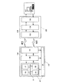
ここで、非接触型薄膜集積回路装置を用いた通信原理を、図18を参照して簡単に説明する。非接触型薄膜集積回路装置を有する商品等を、リーダ/ライタ136にかざすことにより、非接触型薄膜集積回路装置132内のアンテナ回路138が、リーダ/ライタ136のアンテナ回路139から発信される電波を受信し、電源回路26において、共振作用により起電力が発生(電磁誘導等)する。そして、非接触型薄膜集積回路装置132内の薄膜集積回路25(ICチップ)が起動し、チップ内の情報を信号化した後、カード側のアンテナ回路から信号を発信する。該信号をリーダ/ライタ136のアンテナ回路139でキャッチし、コントローラ135を介してデータ処理を行うホストコンピュータ137へ送信される。なお、ホストコンピュータがリーダ/ライタ手段を有していても構わない。また、ICチップのアンテナ回路部は、RF(無線)インタフェース130と、非接触インタフェース131とを、リーダ/ライタのアンテナ回路部は非接触インタフェース133と、インタフェース回路134とを有しているが、この構成に限定されるものではない。
Here, the communication principle using the non-contact type thin film integrated circuit device will be briefly described with reference to FIG. By holding a product or the like having a non-contact type thin film integrated circuit device over the reader /
メモリ29にはROM(Read Only Memory)、RAM(Random Access Memory)、PROM、EPROM又はEEPROM(Electronically Erasable and Programmable ReadOnly Memory)、FRAM(登録商標)(FeRAM;Ferroelectric Random Access Memory)等が利用される。PROMやEPROMの場合はカードを発行する時以外は書込みができないが、EEPROMは書き換えが可能である。これらメモリは、用途に応じて選択すればよい。
The
電源回路26は、例えばダイオードと、容量とを有する構成であればよく、アンテナが受信する交流周波を直流に変換する機能を有している。
The
非接触型のICの特徴は、コイル状に巻かれたアンテナの電磁誘導作用(電磁誘導方式)、相互誘導作用(電磁結合方式)又は静電気による誘導作用(静電結合方式)により電力が供給される点である。このアンテナの巻き数を制御することにより、受信する周波数の高さを選ぶことができる。 The non-contact type IC is characterized in that power is supplied by the electromagnetic induction effect (electromagnetic induction method), mutual induction effect (electromagnetic coupling method) or static induction effect (electrostatic coupling method) of the coiled antenna. It is a point. By controlling the number of turns of the antenna, the height of the frequency to be received can be selected.
なお、図示しないが、暗号処理専用のコプロセッサと呼ばれる演算装置をCPUに接続しても良い。これにより、決済等のアプリケーションを行う際に必要となる暗号処理を行うことができる。 Although not shown, an arithmetic unit called a coprocessor dedicated to cryptographic processing may be connected to the CPU. As a result, it is possible to perform cryptographic processing necessary when performing an application such as payment.
また、生産(製造)者140、販売者141、及び消費者142間の情報や商品の流れを図17に示す。生産(製造)者140は販売者(小売業者、卸業者等)141又は消費者142に薄膜集積回路装置搭載の商品143、144を提供する。そして販売者141は、例えば消費者142の精算時に料金情報、商品の売れ個数や購入時間等の販売情報145を生産(製造)者140に提供することができる。一方消費者142は、個人情報等の購入情報146、147を提供することができる。例えば、薄膜集積回路装置搭載のクレジットカード、又は個人のリーダ等により購入情報を販売者141や生産(製造)者140へネットを介して提供できる。また、販売者141は、薄膜集積回路装置により、消費者に商品情報148を提供し、販売者141は消費者142から購入情報を得ることができる。このような販売情報や購入情報等は、貴重な情報であり、今後の販売戦略に役立つ。
FIG. 17 shows the flow of information and merchandise among producers (manufacturers) 140,
各種情報を提供する手段としては、薄膜集積回路装置から販売者141や消費者142の有するリーダが読み取った情報をコンピュータやネットワークを介して、その情報を生産(製造)者140、販売者141又は消費者142に開示する方法がある。以上のような、多種多様な情報が薄膜集積回路装置を介して必要な者へ提供することができ、本発明に係る薄膜集積回路装置は商品取引又は商品管理上でも有用である。
As means for providing various types of information, information read by readers of the
本実施例では、図19(A)〜図19(C)を参照して、本発明に係る薄膜集積回路装置(IDラベル)搭載の商品において、情報を読み取る方法について説明する。なお本実施の形態では、IDラベルは非接触型である場合で説明する。 In this embodiment, a method for reading information in a product mounted with a thin film integrated circuit device (ID label) according to the present invention will be described with reference to FIGS. In this embodiment, the case where the ID label is a non-contact type will be described.
図19(A)に示すようなリーダ/ライタ本体170のセンサー部171に、IDラベルが搭載された商品172をかざす。そして表示部173には、商品の原材料や原産地、生産(製造)工程ごとの検査結果や流通過程の履歴等が表示され、更に商品の説明等の商品に関する情報を表示させる。もちろんリーダ/ライタに表示部を必ず設ける必要はなく、別に設けられてもよい。このようなリーダ/ライタは商品が陳列されている棚に設置しておけばよい。
A
また図19(B)に示すように、個人が所有する携帯情報端末、例えば携帯電話機本体180に、リーダ機能を搭載させ、本体の一部に設けられたセンサー部181にIDラベルが搭載された商品172をかざし、表示部183に情報を表示させる。すると同様に、商品に関する情報が表示される。もちろんリーダ/ライタに表示部を必ず設ける必要はなく、別に設けられてもよい。
Further, as shown in FIG. 19B, a portable information terminal owned by an individual, for example, a mobile phone
また図19(C)に示すように、個人が所有する携帯可能なリーダ本体190と接続されているセンサー部191にIDラベルが搭載された商品172をかざし、表示部193に情報を掲載させる。すると同様に、商品に関する情報が表示される。もちろんリーダ/ライタに表示部を必ず設ける必要はなく、別に設けられてもよい。
Further, as shown in FIG. 19C, a
本実施例では非接触型のリーダ/ライタについて説明したが、接触型であっても表示部に情報を表示させればよい。また非接触型又は接触型の薄膜集積回路装置が搭載される商品自体に表示部を設け、情報を表示させても構わない。 In this embodiment, a non-contact type reader / writer has been described. However, information may be displayed on a display unit even in a contact type. Further, a display unit may be provided on a product itself on which a non-contact type or contact type thin film integrated circuit device is mounted to display information.
このように、従来の無線タグ等により提供される情報と比べて、消費者は商品に関する豊富な情報を自由に入手することができる。勿論、薄膜集積回路装置により商品管理を素早く正確に行うことができる。 Thus, compared with information provided by a conventional wireless tag or the like, the consumer can freely obtain abundant information regarding the product. Of course, the product management can be performed quickly and accurately by the thin film integrated circuit device.
なお、本発明に係る非接触型の薄膜集積回路は、カードリーダ/ライタとの距離が2m以下である遠隔型、70cm以下である近傍型、10cm以下である近接型、数cmである密着型とすることができ、生産、製造現場での作業を考えると近傍型又は密着型が好ましい。 The non-contact type thin film integrated circuit according to the present invention includes a remote type whose distance to the card reader / writer is 2 m or less, a proximity type which is 70 cm or less, a proximity type which is 10 cm or less, and a contact type which is several cm. In view of production and work at the manufacturing site, the proximity type or the close contact type is preferable.
周波数は、遠隔型ではマイクロ波、2.45GHz、近傍型及び近接型では、13.56MHz、密着型では4.91MHz、125kHzが一般的に使用されているが、周波数を高め波長を短くすることによりアンテナの巻き数を小さくできる。 As for the frequency, microwaves are generally used for the remote type, 2.45 GHz, 13.56 MHz for the proximity type and proximity type, and 4.91 MHz and 125 kHz for the contact type, but the frequency should be increased to shorten the wavelength. Thus, the number of turns of the antenna can be reduced.
また非接触型薄膜集積回路は接触型薄膜集積回路と比較すると、リーダ/ライタに接触せず、非接触で電源供給及び情報通信を行うため、破損せず、高い耐久性を有し、静電気等によるエラーの心配がない。更にはリーダ/ライタ自体の構成は複雑にならならず、薄膜集積回路をリーダ/ライタにかざせばよいので、取り扱いが容易である。 Compared with the contact type thin film integrated circuit, the non-contact type thin film integrated circuit is not in contact with the reader / writer and performs power supply and information communication without contact, so it is not damaged and has high durability, static electricity, etc. There is no worry about errors. Furthermore, the configuration of the reader / writer itself does not become complicated, and the thin film integrated circuit only needs to be held over the reader / writer, so that handling is easy.
本実施例では、図20、図21を参照して、本発明に係る薄膜集積回路、又は非接触型薄膜集積回路装置(無線チップ、IDラベル)を搭載した商品の一例について説明する。 In this embodiment, an example of a product on which the thin film integrated circuit or the non-contact type thin film integrated circuit device (wireless chip, ID label) according to the present invention is mounted will be described with reference to FIGS.
図20(A)は、薄膜集積回路装置201を内蔵した紙幣200であり、他に証券、チケット、T/C(トラベラーズチェック)等であってもよい。図20(B)は、薄膜集積回路装置201を内蔵した硬貨202であり他にメダルであってもよい。図20(C)は、薄膜集積回路装置201を内蔵した住民票、戸籍謄本等の書類203を示している。図20(D)は、薄膜集積回路装置201をブックカバーに内蔵した書籍205を示している。
FIG. 20A shows a
本発明に係る非接触型又は接触型の薄膜集積回路は非常に薄いため、上記紙幣、コイン、書類、書籍等の物品に薄膜集積回路を搭載しても、機能、デザイン性を損ねることがない。更に非接触型薄膜集積回路の場合、アンテナとICとを一体形成でき、曲面を有する商品に直接転写することが容易になる。 Since the non-contact type or contact type thin film integrated circuit according to the present invention is very thin, even if the thin film integrated circuit is mounted on an article such as a banknote, a coin, a document, or a book, the function and design are not impaired. . Further, in the case of a non-contact type thin film integrated circuit, the antenna and the IC can be integrally formed, and it becomes easy to directly transfer the product to a curved product.
図21(A)は、薄膜集積回路装置201を内蔵したカプセル207を示している。カプセル207の内部には、コイル状のアンテナ208が形成されており、外部のリーダ/ライタによって通信を行うことができる。例えば、人間や動物に、カプセル207を服用させることにより、その人間や動物の健康状態等の情報を即座に入手することができる。
FIG. 21A shows a
図21(B)は、薄膜集積回路装置201を内蔵した絆創膏210を示している。ガーゼとなるカバー212の裏側に薄膜集積回路装置201を設けることで通常の絆創膏として使用できる。このように、様々な医療器具等にも、本発明を用いることができる。
FIG. 21B shows an
図21(C)は、薄膜集積回路装置201を内蔵したIDタグ213を示している。IDタグ213を商品に備え付けることにより、商品管理が容易になる。例えば、商品が盗難された場合に、商品の経路を辿ることによって、その犯人を迅速に把握することができる。このように、IDタグを備えることにより、所謂トレーサビリティ(traceablity;複雑化した製造、流通の各段階で問題が生じた場合に、経路を遡ることによって、その原因を迅速に把握できる態勢を整えること。)に優れた商品を流通させることができる。
FIG. 21C shows an
図21(D)は、ラベル台紙217に貼られた薄膜集積回路装置201を内蔵したIDラベル215を示している。IDラベル上には、その商品や役務に関する情報(商品名、ブランド、商標、商標権者、販売者、製造者等)が記されており、一方、内蔵されている薄膜集積回路装置には、その商品(又は商品の種類)固有のIDナンバーが付されており、偽造や、商標権、特許権等の知的財産権侵害、不正競争等の不法行為を容易に把握することができる。また、薄膜集積回路装置内には、商品の容器やラベルに明記しきれない多大な情報、例えば、商品の産地、販売地、品質、原材料、効能、用途、数量、形状、価格、生産方法、使用方法、生産時期、使用時期、賞味期限、取扱説明、商品に関する知的財産情報等を入力しておくことができ、取引者や消費者は、簡易なリーダによって、それらの情報にアクセスすることができる。また、生産者側からは容易に書換え、消去等も可能であるが、取引者、消費者側からは書換え、消去等ができない仕組みになっている。
FIG. 21D shows an
また、図示しないが、人体、動物に有害でない金属や有機材料等を用いた薄膜集積回路装置を作製し、食品等に混入させ、食事状況を管理することも可能である。 Although not shown, it is also possible to manufacture a thin film integrated circuit device using a metal or an organic material that is not harmful to a human body or an animal, mix it with food, etc., and manage a meal situation.
上述した商品以外にも、あらゆる商品に、本発明に係る薄膜集積回路、非接触型薄膜集積回路装置を利用することができる。 In addition to the products described above, the thin film integrated circuit and the non-contact type thin film integrated circuit device according to the present invention can be used for all products.
上記実施形態又は実施例では、主に非接触型薄膜集積回路装置について説明したが、本発明に係る薄膜集積回路は、勿論、接触型薄膜集積回路装置にも採用することができる。例えば、磁気ストライプ型や、ICモジュール接点型のチップとすることができる。接触型ICの場合はアンテナを設けない構成とすればよい。また、これらの磁気ストライプ型又はICモジュール接点型の薄膜集積回路装置と、非接触型薄膜集積回路装置とを組み合わせた構造としても良い。 In the above-described embodiments or examples, the description has been mainly made on the non-contact type thin film integrated circuit device. However, the thin film integrated circuit according to the present invention can of course be applied to a contact type thin film integrated circuit device. For example, a magnetic stripe type or IC module contact type chip can be used. In the case of a contact type IC, an antenna may be omitted. Further, the magnetic stripe type or IC module contact type thin film integrated circuit device may be combined with a non-contact type thin film integrated circuit device.
本発明に係る薄膜集積回路の作製方法、非接触型薄膜集積回路装置並びにその作製方法は、従来のシリコンウエハを用いて作製するICチップの作製方法に比べ、製造コストを大幅に削減することができる。本発明を用いることにより、薄膜集積回路装置に用いられる薄膜集積回路、非接触型薄膜集積回路装置や、それを用いた商品等を、低コストで大量に高歩留まり、高スループットで作製することができる。また、本発明に係る薄膜集積回路の作製方法は、接触型、非接触型薄膜集積回路装置のいずれにも採用することができ、その利用範囲は極めて広い。 The manufacturing method of the thin film integrated circuit, the non-contact type thin film integrated circuit device, and the manufacturing method thereof according to the present invention can greatly reduce the manufacturing cost as compared with the manufacturing method of an IC chip manufactured using a conventional silicon wafer. it can. By using the present invention, a thin film integrated circuit, a non-contact type thin film integrated circuit device used in a thin film integrated circuit device, a product using the thin film integrated circuit device, a product using the thin film integrated circuit device, and the like can be manufactured in a large amount with a high yield and a high throughput. it can. In addition, the method for manufacturing a thin film integrated circuit according to the present invention can be applied to both a contact type and a non-contact type thin film integrated circuit device, and its application range is extremely wide.
43:剥離層
44:下地膜
42、25、87:薄膜集積回路
48、68、20、112:アンテナ
50、66、201:薄膜集積回路装置
51、81:仮接着剤
52、55、76:ジグ(支持基板)
15:IDラベル
49、116:保護膜
10:商品
16、136:リーダ/ライタ
43: peeling layer 44:
15:
Claims (7)
前記剥離層上に下地膜を形成し、
前記下地膜上に複数の薄膜集積回路を形成し、
前記薄膜集積回路上に絶縁膜を形成し、
前記絶縁膜上にコンタクトホールを介して薄膜集積回路と接続する配線を形成し、
前記配線上に保護膜を形成することで前記薄膜集積回路と前記配線を有する薄膜集積回路装置を複数形成し、
前記複数の薄膜集積回路装置の境界に溝を形成し、
前記複数の薄膜集積回路装置の上方である前記保護膜に、複数の突起部を有するジグの当該突起部を、前記薄膜集積回路装置毎に接着し、
前記溝にフッ化ハロゲンを含む気体又は液体を導入し、前記剥離層を除去することによって、前記複数の薄膜集積回路装置を分離し、
前記複数の薄膜集積回路装置に接着されたジグを取り外すことを特徴とする薄膜集積回路装置の作製方法。 Forming a release layer on the substrate,
Forming a base film on the release layer;
A plurality of thin film integrated circuits are formed on the base film,
Forming an insulating film on the thin film integrated circuit;
A wiring connected to the thin film integrated circuit through a contact hole is formed on the insulating film,
Forming a plurality of thin film integrated circuit devices having the thin film integrated circuit and the wiring by forming a protective film on the wiring;
Forming a groove at a boundary between the plurality of thin film integrated circuit devices;
Bonding the protrusions of the jig having a plurality of protrusions to the protective film above the plurality of thin film integrated circuit devices for each of the thin film integrated circuit devices,
Introducing a gas or liquid containing halogen fluoride into the groove and removing the release layer, the plurality of thin film integrated circuit devices are separated,
A method for manufacturing a thin film integrated circuit device, comprising: removing a jig bonded to the plurality of thin film integrated circuit devices.
前記ジグの接着は、UV光によって接着力が低下又は喪失する接着剤を用いて行なうことを特徴とする薄膜集積回路装置の作製方法。 Oite to claim 1,
The method of manufacturing a thin film integrated circuit device, wherein the bonding of the jig is performed using an adhesive whose adhesive strength is reduced or lost by UV light.
前記剥離層は、シリコンを主成分として含むことを特徴とする薄膜集積回路装置の作製方法。 In claim 1 or 2 ,
The method for manufacturing a thin film integrated circuit device, wherein the release layer contains silicon as a main component.
前記下地膜は、酸化珪素、窒化珪素、窒素を含む酸化珪素のいずれかを含むことを特徴とする薄膜集積回路装置の作製方法。 In any one of Claims 1 thru | or 3 ,
The method for manufacturing a thin film integrated circuit device, wherein the base film includes any one of silicon oxide, silicon nitride, and silicon oxide containing nitrogen.
前記溝はダイヤモンドスクライビング又はレーザースクライビングによって形成されることを特徴とする薄膜集積回路装置の作製方法。 In any one of Claims 1 thru | or 4 ,
The method of manufacturing a thin film integrated circuit device, wherein the groove is formed by diamond scribing or laser scribing.
前記基板は、ガラス基板又は石英基板であることを特徴とする薄膜集積回路装置の作製方法。 In any one of Claims 1 thru | or 5 ,
The method for manufacturing a thin film integrated circuit device, wherein the substrate is a glass substrate or a quartz substrate.
前記フッ化ハロゲンは、ClF3(三フッ化塩素)であることを特徴とする薄膜集積回路装置の作製方法。
In any one of Claims 1 thru | or 6 ,
The method for manufacturing a thin film integrated circuit device, wherein the halogen fluoride is ClF 3 (chlorine trifluoride).
Priority Applications (1)
| Application Number | Priority Date | Filing Date | Title |
|---|---|---|---|
| JP2004362339A JP5110766B2 (en) | 2003-12-15 | 2004-12-15 | Method for manufacturing thin film integrated circuit device and method for manufacturing non-contact type thin film integrated circuit device |
Applications Claiming Priority (3)
| Application Number | Priority Date | Filing Date | Title |
|---|---|---|---|
| JP2003417317 | 2003-12-15 | ||
| JP2003417317 | 2003-12-15 | ||
| JP2004362339A JP5110766B2 (en) | 2003-12-15 | 2004-12-15 | Method for manufacturing thin film integrated circuit device and method for manufacturing non-contact type thin film integrated circuit device |
Publications (3)
| Publication Number | Publication Date |
|---|---|
| JP2005203762A JP2005203762A (en) | 2005-07-28 |
| JP2005203762A5 JP2005203762A5 (en) | 2008-01-24 |
| JP5110766B2 true JP5110766B2 (en) | 2012-12-26 |
Family
ID=34829151
Family Applications (1)
| Application Number | Title | Priority Date | Filing Date |
|---|---|---|---|
| JP2004362339A Expired - Fee Related JP5110766B2 (en) | 2003-12-15 | 2004-12-15 | Method for manufacturing thin film integrated circuit device and method for manufacturing non-contact type thin film integrated circuit device |
Country Status (1)
| Country | Link |
|---|---|
| JP (1) | JP5110766B2 (en) |
Families Citing this family (7)
| Publication number | Priority date | Publication date | Assignee | Title |
|---|---|---|---|---|
| CN102683391B (en) | 2004-06-04 | 2015-11-18 | 伊利诺伊大学评议会 | For the manufacture of and the method and apparatus of assembling printable semiconductor elements |
| MY152238A (en) * | 2005-06-02 | 2014-09-15 | Univ Illinois | Printable semiconductor structures and related methods of making and assembling |
| US7176053B1 (en) * | 2005-08-16 | 2007-02-13 | Organicid, Inc. | Laser ablation method for fabricating high performance organic devices |
| JP5196212B2 (en) * | 2006-03-02 | 2013-05-15 | セイコーエプソン株式会社 | Thin film device manufacturing method |
| JP2008047776A (en) * | 2006-08-18 | 2008-02-28 | Semiconductor Energy Lab Co Ltd | Semiconductor apparatus and manufacturing method thereof |
| US8463116B2 (en) | 2008-07-01 | 2013-06-11 | Tap Development Limited Liability Company | Systems for curing deposited material using feedback control |
| KR101046064B1 (en) * | 2008-12-11 | 2011-07-01 | 삼성전기주식회사 | Thin Film Device Manufacturing Method |
Family Cites Families (8)
| Publication number | Priority date | Publication date | Assignee | Title |
|---|---|---|---|---|
| JP2970411B2 (en) * | 1993-08-04 | 1999-11-02 | 株式会社日立製作所 | Semiconductor device |
| JP3809733B2 (en) * | 1998-02-25 | 2006-08-16 | セイコーエプソン株式会社 | Thin film transistor peeling method |
| JP2000020665A (en) * | 1998-06-30 | 2000-01-21 | Toshiba Corp | Semiconductor device |
| FR2796491B1 (en) * | 1999-07-12 | 2001-08-31 | Commissariat Energie Atomique | METHOD FOR TAKING OFF TWO ELEMENTS AND DEVICE FOR IMPLEMENTING SAME |
| JP4748859B2 (en) * | 2000-01-17 | 2011-08-17 | 株式会社半導体エネルギー研究所 | Method for manufacturing light emitting device |
| JP2003142666A (en) * | 2001-07-24 | 2003-05-16 | Seiko Epson Corp | Transfer method for element, method for manufacturing element, integrated circuit, circuit board, electrooptic device, ic card and electronic apparatus |
| JP4467215B2 (en) * | 2001-09-04 | 2010-05-26 | 富士通株式会社 | Method for forming porous insulating film and method for manufacturing semiconductor device |
| JP3956697B2 (en) * | 2001-12-28 | 2007-08-08 | セイコーエプソン株式会社 | Manufacturing method of semiconductor integrated circuit |
-
2004
- 2004-12-15 JP JP2004362339A patent/JP5110766B2/en not_active Expired - Fee Related
Also Published As
| Publication number | Publication date |
|---|---|
| JP2005203762A (en) | 2005-07-28 |
Similar Documents
| Publication | Publication Date | Title |
|---|---|---|
| KR101207442B1 (en) | Method for manufacturing thin film integrated circuit device, noncontact thin film integrated circuit device and method for manufacturing the same, and idtag and coin including the noncontact thin film integrated circuit device | |
| US8136735B2 (en) | ID label, ID card, and ID tag | |
| US7728734B2 (en) | ID label, ID tag, and ID card | |
| JP4939757B2 (en) | ID label, ID tag and ID card | |
| JP6968214B2 (en) | Semiconductor device | |
| US7271076B2 (en) | Manufacturing method of thin film integrated circuit device and manufacturing method of non-contact type thin film integrated circuit device | |
| JP4942998B2 (en) | Semiconductor device and manufacturing method of semiconductor device | |
| JP4776941B2 (en) | Semiconductor device manufacturing method, IC card, IC tag, RFID, transponder, banknote, securities, passport, electronic device, bag, and clothing | |
| US8232556B2 (en) | Semiconductor device | |
| JP4761779B2 (en) | ID labels, ID cards, ID tags, and articles | |
| JP5110766B2 (en) | Method for manufacturing thin film integrated circuit device and method for manufacturing non-contact type thin film integrated circuit device | |
| JP4912586B2 (en) | Method for manufacturing thin film integrated circuit device | |
| JP4671681B2 (en) | Semiconductor device and manufacturing method thereof |
Legal Events
| Date | Code | Title | Description |
|---|---|---|---|
| A521 | Request for written amendment filed |
Free format text: JAPANESE INTERMEDIATE CODE: A523 Effective date: 20071204 |
|
| A621 | Written request for application examination |
Free format text: JAPANESE INTERMEDIATE CODE: A621 Effective date: 20071204 |
|
| A977 | Report on retrieval |
Free format text: JAPANESE INTERMEDIATE CODE: A971007 Effective date: 20110920 |
|
| A131 | Notification of reasons for refusal |
Free format text: JAPANESE INTERMEDIATE CODE: A131 Effective date: 20110927 |
|
| A521 | Request for written amendment filed |
Free format text: JAPANESE INTERMEDIATE CODE: A523 Effective date: 20111116 |
|
| A02 | Decision of refusal |
Free format text: JAPANESE INTERMEDIATE CODE: A02 Effective date: 20120612 |
|
| A521 | Request for written amendment filed |
Free format text: JAPANESE INTERMEDIATE CODE: A523 Effective date: 20120822 |
|
| A911 | Transfer to examiner for re-examination before appeal (zenchi) |
Free format text: JAPANESE INTERMEDIATE CODE: A911 Effective date: 20120829 |
|
| TRDD | Decision of grant or rejection written | ||
| A01 | Written decision to grant a patent or to grant a registration (utility model) |
Free format text: JAPANESE INTERMEDIATE CODE: A01 Effective date: 20121002 |
|
| A01 | Written decision to grant a patent or to grant a registration (utility model) |
Free format text: JAPANESE INTERMEDIATE CODE: A01 |
|
| A61 | First payment of annual fees (during grant procedure) |
Free format text: JAPANESE INTERMEDIATE CODE: A61 Effective date: 20121009 |
|
| FPAY | Renewal fee payment (event date is renewal date of database) |
Free format text: PAYMENT UNTIL: 20151019 Year of fee payment: 3 |
|
| R150 | Certificate of patent or registration of utility model |
Free format text: JAPANESE INTERMEDIATE CODE: R150 |
|
| FPAY | Renewal fee payment (event date is renewal date of database) |
Free format text: PAYMENT UNTIL: 20151019 Year of fee payment: 3 |
|
| R250 | Receipt of annual fees |
Free format text: JAPANESE INTERMEDIATE CODE: R250 |
|
| R250 | Receipt of annual fees |
Free format text: JAPANESE INTERMEDIATE CODE: R250 |
|
| R250 | Receipt of annual fees |
Free format text: JAPANESE INTERMEDIATE CODE: R250 |
|
| LAPS | Cancellation because of no payment of annual fees |