JP5204959B2 - Method for manufacturing semiconductor device - Google Patents
Method for manufacturing semiconductor device Download PDFInfo
- Publication number
- JP5204959B2 JP5204959B2 JP2006175611A JP2006175611A JP5204959B2 JP 5204959 B2 JP5204959 B2 JP 5204959B2 JP 2006175611 A JP2006175611 A JP 2006175611A JP 2006175611 A JP2006175611 A JP 2006175611A JP 5204959 B2 JP5204959 B2 JP 5204959B2
- Authority
- JP
- Japan
- Prior art keywords
- layer
- semiconductor device
- film
- semiconductor
- substrate
- Prior art date
- Legal status (The legal status is an assumption and is not a legal conclusion. Google has not performed a legal analysis and makes no representation as to the accuracy of the status listed.)
- Expired - Fee Related
Links
- 239000004065 semiconductor Substances 0.000 title claims description 234
- 238000000034 method Methods 0.000 title claims description 63
- 238000004519 manufacturing process Methods 0.000 title claims description 44
- 239000000758 substrate Substances 0.000 claims description 99
- 239000012535 impurity Substances 0.000 claims description 91
- 239000000463 material Substances 0.000 claims description 57
- 229920005989 resin Polymers 0.000 claims description 28
- 239000011347 resin Substances 0.000 claims description 28
- VYPSYNLAJGMNEJ-UHFFFAOYSA-N Silicium dioxide Chemical compound O=[Si]=O VYPSYNLAJGMNEJ-UHFFFAOYSA-N 0.000 claims description 20
- 239000000853 adhesive Substances 0.000 claims description 14
- 230000001070 adhesive effect Effects 0.000 claims description 14
- -1 polypropylene Polymers 0.000 claims description 12
- 239000003822 epoxy resin Substances 0.000 claims description 10
- 229920000647 polyepoxide Polymers 0.000 claims description 10
- OKTJSMMVPCPJKN-UHFFFAOYSA-N Carbon Chemical compound [C] OKTJSMMVPCPJKN-UHFFFAOYSA-N 0.000 claims description 4
- 229910052799 carbon Inorganic materials 0.000 claims description 4
- 229920003002 synthetic resin Polymers 0.000 claims description 4
- 239000000057 synthetic resin Substances 0.000 claims description 4
- 229920000728 polyester Polymers 0.000 claims description 3
- 239000000377 silicon dioxide Substances 0.000 claims description 3
- 239000004743 Polypropylene Substances 0.000 claims description 2
- BZHJMEDXRYGGRV-UHFFFAOYSA-N Vinyl chloride Chemical compound ClC=C BZHJMEDXRYGGRV-UHFFFAOYSA-N 0.000 claims description 2
- 239000002657 fibrous material Substances 0.000 claims description 2
- AMGQUBHHOARCQH-UHFFFAOYSA-N indium;oxotin Chemical compound [In].[Sn]=O AMGQUBHHOARCQH-UHFFFAOYSA-N 0.000 claims description 2
- 229920001155 polypropylene Polymers 0.000 claims description 2
- 229920002620 polyvinyl fluoride Polymers 0.000 claims description 2
- 235000012239 silicon dioxide Nutrition 0.000 claims description 2
- 125000000391 vinyl group Chemical group [H]C([*])=C([H])[H] 0.000 claims description 2
- 229920002554 vinyl polymer Polymers 0.000 claims description 2
- 239000010410 layer Substances 0.000 description 487
- 239000010408 film Substances 0.000 description 180
- 230000015572 biosynthetic process Effects 0.000 description 71
- 239000010409 thin film Substances 0.000 description 32
- XUIMIQQOPSSXEZ-UHFFFAOYSA-N Silicon Chemical compound [Si] XUIMIQQOPSSXEZ-UHFFFAOYSA-N 0.000 description 26
- 229910052710 silicon Inorganic materials 0.000 description 26
- 239000010703 silicon Substances 0.000 description 26
- 239000007789 gas Substances 0.000 description 24
- 230000008569 process Effects 0.000 description 23
- 229910052782 aluminium Inorganic materials 0.000 description 22
- 238000005268 plasma chemical vapour deposition Methods 0.000 description 21
- XAGFODPZIPBFFR-UHFFFAOYSA-N aluminium Chemical compound [Al] XAGFODPZIPBFFR-UHFFFAOYSA-N 0.000 description 20
- 238000000206 photolithography Methods 0.000 description 20
- 239000010936 titanium Substances 0.000 description 18
- 239000003990 capacitor Substances 0.000 description 16
- PXHVJJICTQNCMI-UHFFFAOYSA-N Nickel Chemical compound [Ni] PXHVJJICTQNCMI-UHFFFAOYSA-N 0.000 description 15
- 238000000926 separation method Methods 0.000 description 15
- 238000004544 sputter deposition Methods 0.000 description 15
- 229910052814 silicon oxide Inorganic materials 0.000 description 14
- 229910021419 crystalline silicon Inorganic materials 0.000 description 13
- 229910052721 tungsten Inorganic materials 0.000 description 12
- 239000010937 tungsten Substances 0.000 description 12
- IJGRMHOSHXDMSA-UHFFFAOYSA-N Atomic nitrogen Chemical compound N#N IJGRMHOSHXDMSA-UHFFFAOYSA-N 0.000 description 11
- 229910052751 metal Inorganic materials 0.000 description 11
- 239000002184 metal Substances 0.000 description 11
- 239000011368 organic material Substances 0.000 description 11
- 239000002356 single layer Substances 0.000 description 11
- WFKWXMTUELFFGS-UHFFFAOYSA-N tungsten Chemical compound [W] WFKWXMTUELFFGS-UHFFFAOYSA-N 0.000 description 11
- 229910052581 Si3N4 Inorganic materials 0.000 description 10
- RTAQQCXQSZGOHL-UHFFFAOYSA-N Titanium Chemical compound [Ti] RTAQQCXQSZGOHL-UHFFFAOYSA-N 0.000 description 10
- 238000002425 crystallisation Methods 0.000 description 10
- 239000011669 selenium Substances 0.000 description 10
- HQVNEWCFYHHQES-UHFFFAOYSA-N silicon nitride Chemical compound N12[Si]34N5[Si]62N3[Si]51N64 HQVNEWCFYHHQES-UHFFFAOYSA-N 0.000 description 10
- 229910052719 titanium Inorganic materials 0.000 description 10
- UHOVQNZJYSORNB-UHFFFAOYSA-N Benzene Chemical group C1=CC=CC=C1 UHOVQNZJYSORNB-UHFFFAOYSA-N 0.000 description 9
- 230000004888 barrier function Effects 0.000 description 9
- 150000001875 compounds Chemical class 0.000 description 9
- 239000013078 crystal Substances 0.000 description 9
- 230000008025 crystallization Effects 0.000 description 9
- 230000006378 damage Effects 0.000 description 9
- 239000000428 dust Substances 0.000 description 9
- 150000002894 organic compounds Chemical class 0.000 description 9
- 230000001681 protective effect Effects 0.000 description 9
- UFHFLCQGNIYNRP-UHFFFAOYSA-N Hydrogen Chemical compound [H][H] UFHFLCQGNIYNRP-UHFFFAOYSA-N 0.000 description 8
- ZOKXTWBITQBERF-UHFFFAOYSA-N Molybdenum Chemical compound [Mo] ZOKXTWBITQBERF-UHFFFAOYSA-N 0.000 description 8
- 239000001257 hydrogen Substances 0.000 description 8
- 229910052739 hydrogen Inorganic materials 0.000 description 8
- 150000002500 ions Chemical class 0.000 description 8
- 229910052750 molybdenum Inorganic materials 0.000 description 8
- 239000011733 molybdenum Substances 0.000 description 8
- LIVNPJMFVYWSIS-UHFFFAOYSA-N silicon monoxide Chemical compound [Si-]#[O+] LIVNPJMFVYWSIS-UHFFFAOYSA-N 0.000 description 8
- KDLHZDBZIXYQEI-UHFFFAOYSA-N Palladium Chemical compound [Pd] KDLHZDBZIXYQEI-UHFFFAOYSA-N 0.000 description 7
- OAICVXFJPJFONN-UHFFFAOYSA-N Phosphorus Chemical compound [P] OAICVXFJPJFONN-UHFFFAOYSA-N 0.000 description 7
- 239000010949 copper Substances 0.000 description 7
- 235000013305 food Nutrition 0.000 description 7
- 238000010438 heat treatment Methods 0.000 description 7
- 229910044991 metal oxide Inorganic materials 0.000 description 7
- 150000004706 metal oxides Chemical class 0.000 description 7
- 229910052760 oxygen Inorganic materials 0.000 description 7
- 239000012785 packaging film Substances 0.000 description 7
- 229920006280 packaging film Polymers 0.000 description 7
- 229910052698 phosphorus Inorganic materials 0.000 description 7
- 239000011574 phosphorus Substances 0.000 description 7
- 238000012545 processing Methods 0.000 description 7
- 239000000126 substance Substances 0.000 description 7
- 239000000956 alloy Substances 0.000 description 6
- 125000004429 atom Chemical group 0.000 description 6
- 238000001312 dry etching Methods 0.000 description 6
- 238000005530 etching Methods 0.000 description 6
- 230000006870 function Effects 0.000 description 6
- 239000011521 glass Substances 0.000 description 6
- 229910052759 nickel Inorganic materials 0.000 description 6
- 229910052757 nitrogen Inorganic materials 0.000 description 6
- 229910052711 selenium Inorganic materials 0.000 description 6
- 229910052714 tellurium Inorganic materials 0.000 description 6
- ZOXJGFHDIHLPTG-UHFFFAOYSA-N Boron Chemical compound [B] ZOXJGFHDIHLPTG-UHFFFAOYSA-N 0.000 description 5
- KRHYYFGTRYWZRS-UHFFFAOYSA-N Fluorane Chemical compound F KRHYYFGTRYWZRS-UHFFFAOYSA-N 0.000 description 5
- 239000012790 adhesive layer Substances 0.000 description 5
- 229910052787 antimony Inorganic materials 0.000 description 5
- 229910052796 boron Inorganic materials 0.000 description 5
- 230000008859 change Effects 0.000 description 5
- 239000003814 drug Substances 0.000 description 5
- 239000011229 interlayer Substances 0.000 description 5
- 239000001301 oxygen Substances 0.000 description 5
- 238000004806 packaging method and process Methods 0.000 description 5
- 238000009832 plasma treatment Methods 0.000 description 5
- 239000004033 plastic Substances 0.000 description 5
- 229920003023 plastic Polymers 0.000 description 5
- 229910052715 tantalum Inorganic materials 0.000 description 5
- MZLGASXMSKOWSE-UHFFFAOYSA-N tantalum nitride Chemical compound [Ta]#N MZLGASXMSKOWSE-UHFFFAOYSA-N 0.000 description 5
- PORWMNRCUJJQNO-UHFFFAOYSA-N tellurium atom Chemical compound [Te] PORWMNRCUJJQNO-UHFFFAOYSA-N 0.000 description 5
- QGZKDVFQNNGYKY-UHFFFAOYSA-N Ammonia Chemical compound N QGZKDVFQNNGYKY-UHFFFAOYSA-N 0.000 description 4
- XKRFYHLGVUSROY-UHFFFAOYSA-N Argon Chemical compound [Ar] XKRFYHLGVUSROY-UHFFFAOYSA-N 0.000 description 4
- RYGMFSIKBFXOCR-UHFFFAOYSA-N Copper Chemical compound [Cu] RYGMFSIKBFXOCR-UHFFFAOYSA-N 0.000 description 4
- 229910018110 Se—Te Inorganic materials 0.000 description 4
- 238000000137 annealing Methods 0.000 description 4
- QVGXLLKOCUKJST-UHFFFAOYSA-N atomic oxygen Chemical compound [O] QVGXLLKOCUKJST-UHFFFAOYSA-N 0.000 description 4
- 230000005540 biological transmission Effects 0.000 description 4
- 239000011651 chromium Substances 0.000 description 4
- 229910017052 cobalt Inorganic materials 0.000 description 4
- 239000010941 cobalt Substances 0.000 description 4
- GUTLYIVDDKVIGB-UHFFFAOYSA-N cobalt atom Chemical compound [Co] GUTLYIVDDKVIGB-UHFFFAOYSA-N 0.000 description 4
- 229910052802 copper Inorganic materials 0.000 description 4
- 230000036541 health Effects 0.000 description 4
- 229910010272 inorganic material Inorganic materials 0.000 description 4
- 239000011147 inorganic material Substances 0.000 description 4
- 230000001678 irradiating effect Effects 0.000 description 4
- 239000010955 niobium Substances 0.000 description 4
- 239000010948 rhodium Substances 0.000 description 4
- 238000003860 storage Methods 0.000 description 4
- 229910052718 tin Inorganic materials 0.000 description 4
- 229910052779 Neodymium Inorganic materials 0.000 description 3
- MWUXSHHQAYIFBG-UHFFFAOYSA-N Nitric oxide Chemical compound O=[N] MWUXSHHQAYIFBG-UHFFFAOYSA-N 0.000 description 3
- XYFCBTPGUUZFHI-UHFFFAOYSA-N Phosphine Chemical compound P XYFCBTPGUUZFHI-UHFFFAOYSA-N 0.000 description 3
- BUGBHKTXTAQXES-UHFFFAOYSA-N Selenium Chemical compound [Se] BUGBHKTXTAQXES-UHFFFAOYSA-N 0.000 description 3
- BQCADISMDOOEFD-UHFFFAOYSA-N Silver Chemical compound [Ag] BQCADISMDOOEFD-UHFFFAOYSA-N 0.000 description 3
- ATJFFYVFTNAWJD-UHFFFAOYSA-N Tin Chemical compound [Sn] ATJFFYVFTNAWJD-UHFFFAOYSA-N 0.000 description 3
- 239000002253 acid Substances 0.000 description 3
- 230000009471 action Effects 0.000 description 3
- 229910021417 amorphous silicon Inorganic materials 0.000 description 3
- WATWJIUSRGPENY-UHFFFAOYSA-N antimony atom Chemical compound [Sb] WATWJIUSRGPENY-UHFFFAOYSA-N 0.000 description 3
- 229910052786 argon Inorganic materials 0.000 description 3
- 230000008901 benefit Effects 0.000 description 3
- 230000015556 catabolic process Effects 0.000 description 3
- 229910052804 chromium Inorganic materials 0.000 description 3
- 239000004020 conductor Substances 0.000 description 3
- ZOCHARZZJNPSEU-UHFFFAOYSA-N diboron Chemical compound B#B ZOCHARZZJNPSEU-UHFFFAOYSA-N 0.000 description 3
- KPUWHANPEXNPJT-UHFFFAOYSA-N disiloxane Chemical class [SiH3]O[SiH3] KPUWHANPEXNPJT-UHFFFAOYSA-N 0.000 description 3
- 229940079593 drug Drugs 0.000 description 3
- 230000005674 electromagnetic induction Effects 0.000 description 3
- 238000001704 evaporation Methods 0.000 description 3
- 238000000605 extraction Methods 0.000 description 3
- 230000002349 favourable effect Effects 0.000 description 3
- 239000010931 gold Substances 0.000 description 3
- 238000007689 inspection Methods 0.000 description 3
- 238000005499 laser crystallization Methods 0.000 description 3
- QGLKJKCYBOYXKC-UHFFFAOYSA-N nonaoxidotritungsten Chemical compound O=[W]1(=O)O[W](=O)(=O)O[W](=O)(=O)O1 QGLKJKCYBOYXKC-UHFFFAOYSA-N 0.000 description 3
- 229910052763 palladium Inorganic materials 0.000 description 3
- 239000002994 raw material Substances 0.000 description 3
- 229910052709 silver Inorganic materials 0.000 description 3
- 239000004332 silver Substances 0.000 description 3
- GUVRBAGPIYLISA-UHFFFAOYSA-N tantalum atom Chemical compound [Ta] GUVRBAGPIYLISA-UHFFFAOYSA-N 0.000 description 3
- JBQYATWDVHIOAR-UHFFFAOYSA-N tellanylidenegermanium Chemical compound [Te]=[Ge] JBQYATWDVHIOAR-UHFFFAOYSA-N 0.000 description 3
- TVIVIEFSHFOWTE-UHFFFAOYSA-K tri(quinolin-8-yloxy)alumane Chemical compound [Al+3].C1=CN=C2C([O-])=CC=CC2=C1.C1=CN=C2C([O-])=CC=CC2=C1.C1=CN=C2C([O-])=CC=CC2=C1 TVIVIEFSHFOWTE-UHFFFAOYSA-K 0.000 description 3
- 229910001930 tungsten oxide Inorganic materials 0.000 description 3
- 238000001039 wet etching Methods 0.000 description 3
- 239000011701 zinc Substances 0.000 description 3
- IYZMXHQDXZKNCY-UHFFFAOYSA-N 1-n,1-n-diphenyl-4-n,4-n-bis[4-(n-phenylanilino)phenyl]benzene-1,4-diamine Chemical compound C1=CC=CC=C1N(C=1C=CC(=CC=1)N(C=1C=CC(=CC=1)N(C=1C=CC=CC=1)C=1C=CC=CC=1)C=1C=CC(=CC=1)N(C=1C=CC=CC=1)C=1C=CC=CC=1)C1=CC=CC=C1 IYZMXHQDXZKNCY-UHFFFAOYSA-N 0.000 description 2
- SPDPTFAJSFKAMT-UHFFFAOYSA-N 1-n-[4-[4-(n-[4-(3-methyl-n-(3-methylphenyl)anilino)phenyl]anilino)phenyl]phenyl]-4-n,4-n-bis(3-methylphenyl)-1-n-phenylbenzene-1,4-diamine Chemical group CC1=CC=CC(N(C=2C=CC(=CC=2)N(C=2C=CC=CC=2)C=2C=CC(=CC=2)C=2C=CC(=CC=2)N(C=2C=CC=CC=2)C=2C=CC(=CC=2)N(C=2C=C(C)C=CC=2)C=2C=C(C)C=CC=2)C=2C=C(C)C=CC=2)=C1 SPDPTFAJSFKAMT-UHFFFAOYSA-N 0.000 description 2
- ZVFQEOPUXVPSLB-UHFFFAOYSA-N 3-(4-tert-butylphenyl)-4-phenyl-5-(4-phenylphenyl)-1,2,4-triazole Chemical compound C1=CC(C(C)(C)C)=CC=C1C(N1C=2C=CC=CC=2)=NN=C1C1=CC=C(C=2C=CC=CC=2)C=C1 ZVFQEOPUXVPSLB-UHFFFAOYSA-N 0.000 description 2
- DHDHJYNTEFLIHY-UHFFFAOYSA-N 4,7-diphenyl-1,10-phenanthroline Chemical compound C1=CC=CC=C1C1=CC=NC2=C1C=CC1=C(C=3C=CC=CC=3)C=CN=C21 DHDHJYNTEFLIHY-UHFFFAOYSA-N 0.000 description 2
- VIZUPBYFLORCRA-UHFFFAOYSA-N 9,10-dinaphthalen-2-ylanthracene Chemical compound C12=CC=CC=C2C(C2=CC3=CC=CC=C3C=C2)=C(C=CC=C2)C2=C1C1=CC=C(C=CC=C2)C2=C1 VIZUPBYFLORCRA-UHFFFAOYSA-N 0.000 description 2
- VFUDMQLBKNMONU-UHFFFAOYSA-N 9-[4-(4-carbazol-9-ylphenyl)phenyl]carbazole Chemical group C12=CC=CC=C2C2=CC=CC=C2N1C1=CC=C(C=2C=CC(=CC=2)N2C3=CC=CC=C3C3=CC=CC=C32)C=C1 VFUDMQLBKNMONU-UHFFFAOYSA-N 0.000 description 2
- 239000004593 Epoxy Substances 0.000 description 2
- 229910052691 Erbium Inorganic materials 0.000 description 2
- 239000004952 Polyamide Substances 0.000 description 2
- KJTLSVCANCCWHF-UHFFFAOYSA-N Ruthenium Chemical compound [Ru] KJTLSVCANCCWHF-UHFFFAOYSA-N 0.000 description 2
- 229910004283 SiO 4 Inorganic materials 0.000 description 2
- 229910052775 Thulium Inorganic materials 0.000 description 2
- NRTOMJZYCJJWKI-UHFFFAOYSA-N Titanium nitride Chemical compound [Ti]#N NRTOMJZYCJJWKI-UHFFFAOYSA-N 0.000 description 2
- 239000007983 Tris buffer Substances 0.000 description 2
- 229910052769 Ytterbium Inorganic materials 0.000 description 2
- HCHKCACWOHOZIP-UHFFFAOYSA-N Zinc Chemical compound [Zn] HCHKCACWOHOZIP-UHFFFAOYSA-N 0.000 description 2
- NIXOWILDQLNWCW-UHFFFAOYSA-N acrylic acid group Chemical group C(C=C)(=O)O NIXOWILDQLNWCW-UHFFFAOYSA-N 0.000 description 2
- 229910021529 ammonia Inorganic materials 0.000 description 2
- GPBUGPUPKAGMDK-UHFFFAOYSA-N azanylidynemolybdenum Chemical compound [Mo]#N GPBUGPUPKAGMDK-UHFFFAOYSA-N 0.000 description 2
- UFVXQDWNSAGPHN-UHFFFAOYSA-K bis[(2-methylquinolin-8-yl)oxy]-(4-phenylphenoxy)alumane Chemical compound [Al+3].C1=CC=C([O-])C2=NC(C)=CC=C21.C1=CC=C([O-])C2=NC(C)=CC=C21.C1=CC([O-])=CC=C1C1=CC=CC=C1 UFVXQDWNSAGPHN-UHFFFAOYSA-K 0.000 description 2
- 239000000919 ceramic Substances 0.000 description 2
- 238000006243 chemical reaction Methods 0.000 description 2
- 239000000460 chlorine Substances 0.000 description 2
- 239000011248 coating agent Substances 0.000 description 2
- 238000000576 coating method Methods 0.000 description 2
- 238000004891 communication Methods 0.000 description 2
- 229920000547 conjugated polymer Polymers 0.000 description 2
- 238000010168 coupling process Methods 0.000 description 2
- 238000013461 design Methods 0.000 description 2
- 238000010586 diagram Methods 0.000 description 2
- 238000009826 distribution Methods 0.000 description 2
- 239000002019 doping agent Substances 0.000 description 2
- 230000000694 effects Effects 0.000 description 2
- 230000005611 electricity Effects 0.000 description 2
- 230000005284 excitation Effects 0.000 description 2
- 229910052839 forsterite Inorganic materials 0.000 description 2
- 229910052732 germanium Inorganic materials 0.000 description 2
- 238000005247 gettering Methods 0.000 description 2
- PCHJSUWPFVWCPO-UHFFFAOYSA-N gold Chemical compound [Au] PCHJSUWPFVWCPO-UHFFFAOYSA-N 0.000 description 2
- 229910052737 gold Inorganic materials 0.000 description 2
- 229910000040 hydrogen fluoride Inorganic materials 0.000 description 2
- 229910052738 indium Inorganic materials 0.000 description 2
- APFVFJFRJDLVQX-UHFFFAOYSA-N indium atom Chemical compound [In] APFVFJFRJDLVQX-UHFFFAOYSA-N 0.000 description 2
- 238000009616 inductively coupled plasma Methods 0.000 description 2
- 229910052741 iridium Inorganic materials 0.000 description 2
- GKOZUEZYRPOHIO-UHFFFAOYSA-N iridium atom Chemical compound [Ir] GKOZUEZYRPOHIO-UHFFFAOYSA-N 0.000 description 2
- 238000004518 low pressure chemical vapour deposition Methods 0.000 description 2
- 239000011777 magnesium Substances 0.000 description 2
- HCWCAKKEBCNQJP-UHFFFAOYSA-N magnesium orthosilicate Chemical compound [Mg+2].[Mg+2].[O-][Si]([O-])([O-])[O-] HCWCAKKEBCNQJP-UHFFFAOYSA-N 0.000 description 2
- 239000000203 mixture Substances 0.000 description 2
- IBHBKWKFFTZAHE-UHFFFAOYSA-N n-[4-[4-(n-naphthalen-1-ylanilino)phenyl]phenyl]-n-phenylnaphthalen-1-amine Chemical group C1=CC=CC=C1N(C=1C2=CC=CC=C2C=CC=1)C1=CC=C(C=2C=CC(=CC=2)N(C=2C=CC=CC=2)C=2C3=CC=CC=C3C=CC=2)C=C1 IBHBKWKFFTZAHE-UHFFFAOYSA-N 0.000 description 2
- 229910052758 niobium Inorganic materials 0.000 description 2
- GUCVJGMIXFAOAE-UHFFFAOYSA-N niobium atom Chemical compound [Nb] GUCVJGMIXFAOAE-UHFFFAOYSA-N 0.000 description 2
- 230000003287 optical effect Effects 0.000 description 2
- 230000010355 oscillation Effects 0.000 description 2
- 229910052762 osmium Inorganic materials 0.000 description 2
- SYQBFIAQOQZEGI-UHFFFAOYSA-N osmium atom Chemical compound [Os] SYQBFIAQOQZEGI-UHFFFAOYSA-N 0.000 description 2
- 238000007254 oxidation reaction Methods 0.000 description 2
- YRZZLAGRKZIJJI-UHFFFAOYSA-N oxyvanadium phthalocyanine Chemical compound [V+2]=O.C12=CC=CC=C2C(N=C2[N-]C(C3=CC=CC=C32)=N2)=NC1=NC([C]1C=CC=CC1=1)=NC=1N=C1[C]3C=CC=CC3=C2[N-]1 YRZZLAGRKZIJJI-UHFFFAOYSA-N 0.000 description 2
- 238000000059 patterning Methods 0.000 description 2
- IEQIEDJGQAUEQZ-UHFFFAOYSA-N phthalocyanine Chemical compound N1C(N=C2C3=CC=CC=C3C(N=C3C4=CC=CC=C4C(=N4)N3)=N2)=C(C=CC=C2)C2=C1N=C1C2=CC=CC=C2C4=N1 IEQIEDJGQAUEQZ-UHFFFAOYSA-N 0.000 description 2
- 229920002647 polyamide Polymers 0.000 description 2
- 229910021420 polycrystalline silicon Inorganic materials 0.000 description 2
- 150000003254 radicals Chemical class 0.000 description 2
- 230000009467 reduction Effects 0.000 description 2
- 229910052703 rhodium Inorganic materials 0.000 description 2
- MHOVAHRLVXNVSD-UHFFFAOYSA-N rhodium atom Chemical compound [Rh] MHOVAHRLVXNVSD-UHFFFAOYSA-N 0.000 description 2
- 229910052707 ruthenium Inorganic materials 0.000 description 2
- 150000003839 salts Chemical class 0.000 description 2
- 230000008054 signal transmission Effects 0.000 description 2
- 230000003068 static effect Effects 0.000 description 2
- 125000001424 substituent group Chemical group 0.000 description 2
- 229910052717 sulfur Inorganic materials 0.000 description 2
- 229910052725 zinc Inorganic materials 0.000 description 2
- MCVVDMSWCQUKEV-UHFFFAOYSA-N (2-nitrophenyl)methyl 4-methylbenzenesulfonate Chemical compound C1=CC(C)=CC=C1S(=O)(=O)OCC1=CC=CC=C1[N+]([O-])=O MCVVDMSWCQUKEV-UHFFFAOYSA-N 0.000 description 1
- DTZWGKCFKSJGPK-VOTSOKGWSA-N (e)-2-(2-methyl-6-(2-(1,1,7,7-tetramethyl-1,2,3,5,6,7-hexahydropyrido[3,2,1-ij]quinolin-9-yl)vinyl)-4h-pyran-4-ylidene)malononitrile Chemical compound O1C(C)=CC(=C(C#N)C#N)C=C1\C=C\C1=CC(C(CCN2CCC3(C)C)(C)C)=C2C3=C1 DTZWGKCFKSJGPK-VOTSOKGWSA-N 0.000 description 1
- FNDFKMXAOATGJU-UHFFFAOYSA-N 1-phenyl-2-sulfonylethanone Chemical class O=S(=O)=CC(=O)C1=CC=CC=C1 FNDFKMXAOATGJU-UHFFFAOYSA-N 0.000 description 1
- SNTWKPAKVQFCCF-UHFFFAOYSA-N 2,3-dihydro-1h-triazole Chemical compound N1NC=CN1 SNTWKPAKVQFCCF-UHFFFAOYSA-N 0.000 description 1
- BFTIPCRZWILUIY-UHFFFAOYSA-N 2,5,8,11-tetratert-butylperylene Chemical group CC(C)(C)C1=CC(C2=CC(C(C)(C)C)=CC=3C2=C2C=C(C=3)C(C)(C)C)=C3C2=CC(C(C)(C)C)=CC3=C1 BFTIPCRZWILUIY-UHFFFAOYSA-N 0.000 description 1
- STTGYIUESPWXOW-UHFFFAOYSA-N 2,9-dimethyl-4,7-diphenyl-1,10-phenanthroline Chemical compound C=12C=CC3=C(C=4C=CC=CC=4)C=C(C)N=C3C2=NC(C)=CC=1C1=CC=CC=C1 STTGYIUESPWXOW-UHFFFAOYSA-N 0.000 description 1
- UOCMXZLNHQBBOS-UHFFFAOYSA-N 2-(1,3-benzoxazol-2-yl)phenol zinc Chemical compound [Zn].Oc1ccccc1-c1nc2ccccc2o1.Oc1ccccc1-c1nc2ccccc2o1 UOCMXZLNHQBBOS-UHFFFAOYSA-N 0.000 description 1
- FQJQNLKWTRGIEB-UHFFFAOYSA-N 2-(4-tert-butylphenyl)-5-[3-[5-(4-tert-butylphenyl)-1,3,4-oxadiazol-2-yl]phenyl]-1,3,4-oxadiazole Chemical compound C1=CC(C(C)(C)C)=CC=C1C1=NN=C(C=2C=C(C=CC=2)C=2OC(=NN=2)C=2C=CC(=CC=2)C(C)(C)C)O1 FQJQNLKWTRGIEB-UHFFFAOYSA-N 0.000 description 1
- HONWGFNQCPRRFM-UHFFFAOYSA-N 2-n-(3-methylphenyl)-1-n,1-n,2-n-triphenylbenzene-1,2-diamine Chemical compound CC1=CC=CC(N(C=2C=CC=CC=2)C=2C(=CC=CC=2)N(C=2C=CC=CC=2)C=2C=CC=CC=2)=C1 HONWGFNQCPRRFM-UHFFFAOYSA-N 0.000 description 1
- OBAJPWYDYFEBTF-UHFFFAOYSA-N 2-tert-butyl-9,10-dinaphthalen-2-ylanthracene Chemical compound C1=CC=CC2=CC(C3=C4C=CC=CC4=C(C=4C=C5C=CC=CC5=CC=4)C4=CC=C(C=C43)C(C)(C)C)=CC=C21 OBAJPWYDYFEBTF-UHFFFAOYSA-N 0.000 description 1
- OGGKVJMNFFSDEV-UHFFFAOYSA-N 3-methyl-n-[4-[4-(n-(3-methylphenyl)anilino)phenyl]phenyl]-n-phenylaniline Chemical group CC1=CC=CC(N(C=2C=CC=CC=2)C=2C=CC(=CC=2)C=2C=CC(=CC=2)N(C=2C=CC=CC=2)C=2C=C(C)C=CC=2)=C1 OGGKVJMNFFSDEV-UHFFFAOYSA-N 0.000 description 1
- 125000004860 4-ethylphenyl group Chemical group [H]C1=C([H])C(=C([H])C([H])=C1*)C([H])([H])C([H])([H])[H] 0.000 description 1
- SCZWJXTUYYSKGF-UHFFFAOYSA-N 5,12-dimethylquinolino[2,3-b]acridine-7,14-dione Chemical compound CN1C2=CC=CC=C2C(=O)C2=C1C=C1C(=O)C3=CC=CC=C3N(C)C1=C2 SCZWJXTUYYSKGF-UHFFFAOYSA-N 0.000 description 1
- FCNCGHJSNVOIKE-UHFFFAOYSA-N 9,10-diphenylanthracene Chemical compound C1=CC=CC=C1C(C1=CC=CC=C11)=C(C=CC=C2)C2=C1C1=CC=CC=C1 FCNCGHJSNVOIKE-UHFFFAOYSA-N 0.000 description 1
- SXGIRTCIFPJUEQ-UHFFFAOYSA-N 9-anthracen-9-ylanthracene Chemical group C1=CC=CC2=CC3=CC=CC=C3C(C=3C4=CC=CC=C4C=C4C=CC=CC4=3)=C21 SXGIRTCIFPJUEQ-UHFFFAOYSA-N 0.000 description 1
- 229920000178 Acrylic resin Polymers 0.000 description 1
- MSDMPJCOOXURQD-UHFFFAOYSA-N C545T Chemical compound C1=CC=C2SC(C3=CC=4C=C5C6=C(C=4OC3=O)C(C)(C)CCN6CCC5(C)C)=NC2=C1 MSDMPJCOOXURQD-UHFFFAOYSA-N 0.000 description 1
- 101100481016 Caenorhabditis elegans tag-325 gene Proteins 0.000 description 1
- VYZAMTAEIAYCRO-UHFFFAOYSA-N Chromium Chemical compound [Cr] VYZAMTAEIAYCRO-UHFFFAOYSA-N 0.000 description 1
- 229910017535 Cu-Al-Ni Inorganic materials 0.000 description 1
- GYHNNYVSQQEPJS-UHFFFAOYSA-N Gallium Chemical compound [Ga] GYHNNYVSQQEPJS-UHFFFAOYSA-N 0.000 description 1
- 229910005939 Ge—Sn Inorganic materials 0.000 description 1
- 241001465754 Metazoa Species 0.000 description 1
- ZCQWOFVYLHDMMC-UHFFFAOYSA-N Oxazole Chemical compound C1=COC=N1 ZCQWOFVYLHDMMC-UHFFFAOYSA-N 0.000 description 1
- 239000004642 Polyimide Substances 0.000 description 1
- 229910002808 Si–O–Si Inorganic materials 0.000 description 1
- 229910018731 Sn—Au Inorganic materials 0.000 description 1
- NINIDFKCEFEMDL-UHFFFAOYSA-N Sulfur Chemical compound [S] NINIDFKCEFEMDL-UHFFFAOYSA-N 0.000 description 1
- FZWLAAWBMGSTSO-UHFFFAOYSA-N Thiazole Chemical compound C1=CSC=N1 FZWLAAWBMGSTSO-UHFFFAOYSA-N 0.000 description 1
- GWEVSGVZZGPLCZ-UHFFFAOYSA-N Titan oxide Chemical compound O=[Ti]=O GWEVSGVZZGPLCZ-UHFFFAOYSA-N 0.000 description 1
- WGLPBDUCMAPZCE-UHFFFAOYSA-N Trioxochromium Chemical compound O=[Cr](=O)=O WGLPBDUCMAPZCE-UHFFFAOYSA-N 0.000 description 1
- XTXRWKRVRITETP-UHFFFAOYSA-N Vinyl acetate Chemical compound CC(=O)OC=C XTXRWKRVRITETP-UHFFFAOYSA-N 0.000 description 1
- 229910009372 YVO4 Inorganic materials 0.000 description 1
- QCWXUUIWCKQGHC-UHFFFAOYSA-N Zirconium Chemical compound [Zr] QCWXUUIWCKQGHC-UHFFFAOYSA-N 0.000 description 1
- XHCLAFWTIXFWPH-UHFFFAOYSA-N [O-2].[O-2].[O-2].[O-2].[O-2].[V+5].[V+5] Chemical compound [O-2].[O-2].[O-2].[O-2].[O-2].[V+5].[V+5] XHCLAFWTIXFWPH-UHFFFAOYSA-N 0.000 description 1
- 230000002159 abnormal effect Effects 0.000 description 1
- 239000003522 acrylic cement Substances 0.000 description 1
- 239000003905 agrochemical Substances 0.000 description 1
- 125000000217 alkyl group Chemical group 0.000 description 1
- CSDREXVUYHZDNP-UHFFFAOYSA-N alumanylidynesilicon Chemical compound [Al].[Si] CSDREXVUYHZDNP-UHFFFAOYSA-N 0.000 description 1
- 150000001454 anthracenes Chemical class 0.000 description 1
- 150000004982 aromatic amines Chemical class 0.000 description 1
- 150000004945 aromatic hydrocarbons Chemical class 0.000 description 1
- 229910052785 arsenic Inorganic materials 0.000 description 1
- RQNWIZPPADIBDY-UHFFFAOYSA-N arsenic atom Chemical compound [As] RQNWIZPPADIBDY-UHFFFAOYSA-N 0.000 description 1
- 125000005410 aryl sulfonium group Chemical group 0.000 description 1
- 235000013405 beer Nutrition 0.000 description 1
- 238000005452 bending Methods 0.000 description 1
- UMIVXZPTRXBADB-UHFFFAOYSA-N benzocyclobutene Chemical compound C1=CC=C2CCC2=C1 UMIVXZPTRXBADB-UHFFFAOYSA-N 0.000 description 1
- GQVWHWAWLPCBHB-UHFFFAOYSA-L beryllium;benzo[h]quinolin-10-olate Chemical compound [Be+2].C1=CC=NC2=C3C([O-])=CC=CC3=CC=C21.C1=CC=NC2=C3C([O-])=CC=CC3=CC=C21 GQVWHWAWLPCBHB-UHFFFAOYSA-L 0.000 description 1
- 235000013361 beverage Nutrition 0.000 description 1
- 229910052797 bismuth Inorganic materials 0.000 description 1
- JCXGWMGPZLAOME-UHFFFAOYSA-N bismuth atom Chemical compound [Bi] JCXGWMGPZLAOME-UHFFFAOYSA-N 0.000 description 1
- 230000000903 blocking effect Effects 0.000 description 1
- 239000000872 buffer Substances 0.000 description 1
- XZCJVWCMJYNSQO-UHFFFAOYSA-N butyl pbd Chemical compound C1=CC(C(C)(C)C)=CC=C1C1=NN=C(C=2C=CC(=CC=2)C=2C=CC=CC=2)O1 XZCJVWCMJYNSQO-UHFFFAOYSA-N 0.000 description 1
- BRPQOXSCLDDYGP-UHFFFAOYSA-N calcium oxide Chemical compound [O-2].[Ca+2] BRPQOXSCLDDYGP-UHFFFAOYSA-N 0.000 description 1
- 239000000292 calcium oxide Substances 0.000 description 1
- ODINCKMPIJJUCX-UHFFFAOYSA-N calcium oxide Inorganic materials [Ca]=O ODINCKMPIJJUCX-UHFFFAOYSA-N 0.000 description 1
- 239000000969 carrier Substances 0.000 description 1
- 239000003795 chemical substances by application Substances 0.000 description 1
- 238000005229 chemical vapour deposition Methods 0.000 description 1
- 229910000423 chromium oxide Inorganic materials 0.000 description 1
- 238000010549 co-Evaporation Methods 0.000 description 1
- 150000004696 coordination complex Chemical class 0.000 description 1
- XCJYREBRNVKWGJ-UHFFFAOYSA-N copper(II) phthalocyanine Chemical compound [Cu+2].C12=CC=CC=C2C(N=C2[N-]C(C3=CC=CC=C32)=N2)=NC1=NC([C]1C=CC=CC1=1)=NC=1N=C1[C]3C=CC=CC3=C2[N-]1 XCJYREBRNVKWGJ-UHFFFAOYSA-N 0.000 description 1
- VBVAVBCYMYWNOU-UHFFFAOYSA-N coumarin 6 Chemical compound C1=CC=C2SC(C3=CC4=CC=C(C=C4OC3=O)N(CC)CC)=NC2=C1 VBVAVBCYMYWNOU-UHFFFAOYSA-N 0.000 description 1
- 238000006356 dehydrogenation reaction Methods 0.000 description 1
- 238000000151 deposition Methods 0.000 description 1
- 230000006866 deterioration Effects 0.000 description 1
- BKMIWBZIQAAZBD-UHFFFAOYSA-N diindenoperylene Chemical compound C12=C3C4=CC=C2C2=CC=CC=C2C1=CC=C3C1=CC=C2C3=CC=CC=C3C3=CC=C4C1=C32 BKMIWBZIQAAZBD-UHFFFAOYSA-N 0.000 description 1
- 230000009977 dual effect Effects 0.000 description 1
- 235000013399 edible fruits Nutrition 0.000 description 1
- 229920001971 elastomer Polymers 0.000 description 1
- 238000005516 engineering process Methods 0.000 description 1
- 230000008020 evaporation Effects 0.000 description 1
- 239000000284 extract Substances 0.000 description 1
- 238000000855 fermentation Methods 0.000 description 1
- 230000004151 fermentation Effects 0.000 description 1
- 230000005669 field effect Effects 0.000 description 1
- 125000001153 fluoro group Chemical group F* 0.000 description 1
- 239000011888 foil Substances 0.000 description 1
- 229910052733 gallium Inorganic materials 0.000 description 1
- GNPVGFCGXDBREM-UHFFFAOYSA-N germanium atom Chemical compound [Ge] GNPVGFCGXDBREM-UHFFFAOYSA-N 0.000 description 1
- 230000009477 glass transition Effects 0.000 description 1
- 229910000449 hafnium oxide Inorganic materials 0.000 description 1
- WIHZLLGSGQNAGK-UHFFFAOYSA-N hafnium(4+);oxygen(2-) Chemical compound [O-2].[O-2].[Hf+4] WIHZLLGSGQNAGK-UHFFFAOYSA-N 0.000 description 1
- 229910052736 halogen Inorganic materials 0.000 description 1
- RBTKNAXYKSUFRK-UHFFFAOYSA-N heliogen blue Chemical compound [Cu].[N-]1C2=C(C=CC=C3)C3=C1N=C([N-]1)C3=CC=CC=C3C1=NC([N-]1)=C(C=CC=C3)C3=C1N=C([N-]1)C3=CC=CC=C3C1=N2 RBTKNAXYKSUFRK-UHFFFAOYSA-N 0.000 description 1
- 230000001771 impaired effect Effects 0.000 description 1
- 229910003471 inorganic composite material Inorganic materials 0.000 description 1
- 238000009413 insulation Methods 0.000 description 1
- 230000010354 integration Effects 0.000 description 1
- 238000005468 ion implantation Methods 0.000 description 1
- 238000003475 lamination Methods 0.000 description 1
- 238000005224 laser annealing Methods 0.000 description 1
- 239000003446 ligand Substances 0.000 description 1
- 239000007788 liquid Substances 0.000 description 1
- 239000004973 liquid crystal related substance Substances 0.000 description 1
- FUJCRWPEOMXPAD-UHFFFAOYSA-N lithium oxide Chemical compound [Li+].[Li+].[O-2] FUJCRWPEOMXPAD-UHFFFAOYSA-N 0.000 description 1
- 229910001947 lithium oxide Inorganic materials 0.000 description 1
- 244000144972 livestock Species 0.000 description 1
- 239000000395 magnesium oxide Substances 0.000 description 1
- CPLXHLVBOLITMK-UHFFFAOYSA-N magnesium oxide Inorganic materials [Mg]=O CPLXHLVBOLITMK-UHFFFAOYSA-N 0.000 description 1
- AXZKOIWUVFPNLO-UHFFFAOYSA-N magnesium;oxygen(2-) Chemical compound [O-2].[Mg+2] AXZKOIWUVFPNLO-UHFFFAOYSA-N 0.000 description 1
- 239000011159 matrix material Substances 0.000 description 1
- 150000002739 metals Chemical class 0.000 description 1
- 229910000476 molybdenum oxide Inorganic materials 0.000 description 1
- 229910021421 monocrystalline silicon Inorganic materials 0.000 description 1
- QKCGXXHCELUCKW-UHFFFAOYSA-N n-[4-[4-(dinaphthalen-2-ylamino)phenyl]phenyl]-n-naphthalen-2-ylnaphthalen-2-amine Chemical compound C1=CC=CC2=CC(N(C=3C=CC(=CC=3)C=3C=CC(=CC=3)N(C=3C=C4C=CC=CC4=CC=3)C=3C=C4C=CC=CC4=CC=3)C3=CC4=CC=CC=C4C=C3)=CC=C21 QKCGXXHCELUCKW-UHFFFAOYSA-N 0.000 description 1
- QEFYFXOXNSNQGX-UHFFFAOYSA-N neodymium atom Chemical compound [Nd] QEFYFXOXNSNQGX-UHFFFAOYSA-N 0.000 description 1
- 229910000484 niobium oxide Inorganic materials 0.000 description 1
- URLJKFSTXLNXLG-UHFFFAOYSA-N niobium(5+);oxygen(2-) Chemical compound [O-2].[O-2].[O-2].[O-2].[O-2].[Nb+5].[Nb+5] URLJKFSTXLNXLG-UHFFFAOYSA-N 0.000 description 1
- 150000004767 nitrides Chemical class 0.000 description 1
- 238000005121 nitriding Methods 0.000 description 1
- 239000012299 nitrogen atmosphere Substances 0.000 description 1
- 150000002831 nitrogen free-radicals Chemical class 0.000 description 1
- 125000000962 organic group Chemical group 0.000 description 1
- 230000003647 oxidation Effects 0.000 description 1
- 230000001590 oxidative effect Effects 0.000 description 1
- PQQKPALAQIIWST-UHFFFAOYSA-N oxomolybdenum Chemical compound [Mo]=O PQQKPALAQIIWST-UHFFFAOYSA-N 0.000 description 1
- DYIZHKNUQPHNJY-UHFFFAOYSA-N oxorhenium Chemical compound [Re]=O DYIZHKNUQPHNJY-UHFFFAOYSA-N 0.000 description 1
- BPUBBGLMJRNUCC-UHFFFAOYSA-N oxygen(2-);tantalum(5+) Chemical compound [O-2].[O-2].[O-2].[O-2].[O-2].[Ta+5].[Ta+5] BPUBBGLMJRNUCC-UHFFFAOYSA-N 0.000 description 1
- RVTZCBVAJQQJTK-UHFFFAOYSA-N oxygen(2-);zirconium(4+) Chemical compound [O-2].[O-2].[Zr+4] RVTZCBVAJQQJTK-UHFFFAOYSA-N 0.000 description 1
- 125000006503 p-nitrobenzyl group Chemical group [H]C1=C([H])C(=C([H])C([H])=C1[N+]([O-])=O)C([H])([H])* 0.000 description 1
- 230000002093 peripheral effect Effects 0.000 description 1
- 239000012071 phase Substances 0.000 description 1
- 239000012782 phase change material Substances 0.000 description 1
- 238000002294 plasma sputter deposition Methods 0.000 description 1
- 229920000553 poly(phenylenevinylene) Polymers 0.000 description 1
- 229920001197 polyacetylene Polymers 0.000 description 1
- 229920000767 polyaniline Polymers 0.000 description 1
- 229920001721 polyimide Polymers 0.000 description 1
- 229920002495 polyphenylene ethynylene polymer Polymers 0.000 description 1
- 229920000123 polythiophene Polymers 0.000 description 1
- CHWRSCGUEQEHOH-UHFFFAOYSA-N potassium oxide Chemical compound [O-2].[K+].[K+] CHWRSCGUEQEHOH-UHFFFAOYSA-N 0.000 description 1
- 229910001950 potassium oxide Inorganic materials 0.000 description 1
- 239000000843 powder Substances 0.000 description 1
- 238000007639 printing Methods 0.000 description 1
- 230000001737 promoting effect Effects 0.000 description 1
- 229910003449 rhenium oxide Inorganic materials 0.000 description 1
- 239000010979 ruby Substances 0.000 description 1
- 229910001750 ruby Inorganic materials 0.000 description 1
- 229910001925 ruthenium oxide Inorganic materials 0.000 description 1
- WOCIAKWEIIZHES-UHFFFAOYSA-N ruthenium(iv) oxide Chemical compound O=[Ru]=O WOCIAKWEIIZHES-UHFFFAOYSA-N 0.000 description 1
- VSZWPYCFIRKVQL-UHFFFAOYSA-N selanylidenegallium;selenium Chemical compound [Se].[Se]=[Ga].[Se]=[Ga] VSZWPYCFIRKVQL-UHFFFAOYSA-N 0.000 description 1
- BSWGGJHLVUUXTL-UHFFFAOYSA-N silver zinc Chemical compound [Zn].[Ag] BSWGGJHLVUUXTL-UHFFFAOYSA-N 0.000 description 1
- KKCBUQHMOMHUOY-UHFFFAOYSA-N sodium oxide Chemical compound [O-2].[Na+].[Na+] KKCBUQHMOMHUOY-UHFFFAOYSA-N 0.000 description 1
- 229910001948 sodium oxide Inorganic materials 0.000 description 1
- 239000007787 solid Substances 0.000 description 1
- 239000007790 solid phase Substances 0.000 description 1
- 238000003746 solid phase reaction Methods 0.000 description 1
- 239000000243 solution Substances 0.000 description 1
- 239000011593 sulfur Substances 0.000 description 1
- 229910001936 tantalum oxide Inorganic materials 0.000 description 1
- 229910052716 thallium Inorganic materials 0.000 description 1
- BKVIYDNLLOSFOA-UHFFFAOYSA-N thallium Chemical compound [Tl] BKVIYDNLLOSFOA-UHFFFAOYSA-N 0.000 description 1
- 238000007725 thermal activation Methods 0.000 description 1
- 229920002803 thermoplastic polyurethane Polymers 0.000 description 1
- 229920001187 thermosetting polymer Polymers 0.000 description 1
- OGIDPMRJRNCKJF-UHFFFAOYSA-N titanium oxide Inorganic materials [Ti]=O OGIDPMRJRNCKJF-UHFFFAOYSA-N 0.000 description 1
- 238000012546 transfer Methods 0.000 description 1
- FQFKTKUFHWNTBN-UHFFFAOYSA-N trifluoro-$l^{3}-bromane Chemical compound FBr(F)F FQFKTKUFHWNTBN-UHFFFAOYSA-N 0.000 description 1
- JOHWNGGYGAVMGU-UHFFFAOYSA-N trifluorochlorine Chemical compound FCl(F)F JOHWNGGYGAVMGU-UHFFFAOYSA-N 0.000 description 1
- 229910001935 vanadium oxide Inorganic materials 0.000 description 1
- 238000007740 vapor deposition Methods 0.000 description 1
- 235000013311 vegetables Nutrition 0.000 description 1
- 229920006163 vinyl copolymer Polymers 0.000 description 1
- XLYOFNOQVPJJNP-UHFFFAOYSA-N water Substances O XLYOFNOQVPJJNP-UHFFFAOYSA-N 0.000 description 1
- GWDUZCIBPDVBJM-UHFFFAOYSA-L zinc;2-(2-hydroxyphenyl)-3h-1,3-benzothiazole-2-carboxylate Chemical compound [Zn+2].OC1=CC=CC=C1C1(C([O-])=O)SC2=CC=CC=C2N1.OC1=CC=CC=C1C1(C([O-])=O)SC2=CC=CC=C2N1 GWDUZCIBPDVBJM-UHFFFAOYSA-L 0.000 description 1
- QEPMORHSGFRDLW-UHFFFAOYSA-L zinc;2-(2-hydroxyphenyl)-3h-1,3-benzoxazole-2-carboxylate Chemical compound [Zn+2].OC1=CC=CC=C1C1(C([O-])=O)OC2=CC=CC=C2N1.OC1=CC=CC=C1C1(C([O-])=O)OC2=CC=CC=C2N1 QEPMORHSGFRDLW-UHFFFAOYSA-L 0.000 description 1
- 229910052726 zirconium Inorganic materials 0.000 description 1
- 229910001928 zirconium oxide Inorganic materials 0.000 description 1
Images


Classifications
-
- H—ELECTRICITY
- H01—ELECTRIC ELEMENTS
- H01L—SEMICONDUCTOR DEVICES NOT COVERED BY CLASS H10
- H01L23/00—Details of semiconductor or other solid state devices
- H01L23/28—Encapsulations, e.g. encapsulating layers, coatings, e.g. for protection
- H01L23/29—Encapsulations, e.g. encapsulating layers, coatings, e.g. for protection characterised by the material, e.g. carbon
- H01L23/293—Organic, e.g. plastic
-
- H—ELECTRICITY
- H01—ELECTRIC ELEMENTS
- H01L—SEMICONDUCTOR DEVICES NOT COVERED BY CLASS H10
- H01L27/00—Devices consisting of a plurality of semiconductor or other solid-state components formed in or on a common substrate
- H01L27/02—Devices consisting of a plurality of semiconductor or other solid-state components formed in or on a common substrate including semiconductor components specially adapted for rectifying, oscillating, amplifying or switching and having potential barriers; including integrated passive circuit elements having potential barriers
- H01L27/12—Devices consisting of a plurality of semiconductor or other solid-state components formed in or on a common substrate including semiconductor components specially adapted for rectifying, oscillating, amplifying or switching and having potential barriers; including integrated passive circuit elements having potential barriers the substrate being other than a semiconductor body, e.g. an insulating body
-
- H—ELECTRICITY
- H01—ELECTRIC ELEMENTS
- H01L—SEMICONDUCTOR DEVICES NOT COVERED BY CLASS H10
- H01L21/00—Processes or apparatus adapted for the manufacture or treatment of semiconductor or solid state devices or of parts thereof
- H01L21/02—Manufacture or treatment of semiconductor devices or of parts thereof
- H01L21/04—Manufacture or treatment of semiconductor devices or of parts thereof the devices having potential barriers, e.g. a PN junction, depletion layer or carrier concentration layer
- H01L21/50—Assembly of semiconductor devices using processes or apparatus not provided for in a single one of the subgroups H01L21/06 - H01L21/326, e.g. sealing of a cap to a base of a container
- H01L21/56—Encapsulations, e.g. encapsulation layers, coatings
-
- H—ELECTRICITY
- H01—ELECTRIC ELEMENTS
- H01L—SEMICONDUCTOR DEVICES NOT COVERED BY CLASS H10
- H01L23/00—Details of semiconductor or other solid state devices
- H01L23/48—Arrangements for conducting electric current to or from the solid state body in operation, e.g. leads, terminal arrangements ; Selection of materials therefor
- H01L23/488—Arrangements for conducting electric current to or from the solid state body in operation, e.g. leads, terminal arrangements ; Selection of materials therefor consisting of soldered or bonded constructions
- H01L23/498—Leads, i.e. metallisations or lead-frames on insulating substrates, e.g. chip carriers
- H01L23/49855—Leads, i.e. metallisations or lead-frames on insulating substrates, e.g. chip carriers for flat-cards, e.g. credit cards
-
- H—ELECTRICITY
- H01—ELECTRIC ELEMENTS
- H01L—SEMICONDUCTOR DEVICES NOT COVERED BY CLASS H10
- H01L23/00—Details of semiconductor or other solid state devices
- H01L23/58—Structural electrical arrangements for semiconductor devices not otherwise provided for, e.g. in combination with batteries
- H01L23/64—Impedance arrangements
- H01L23/66—High-frequency adaptations
-
- H—ELECTRICITY
- H01—ELECTRIC ELEMENTS
- H01L—SEMICONDUCTOR DEVICES NOT COVERED BY CLASS H10
- H01L27/00—Devices consisting of a plurality of semiconductor or other solid-state components formed in or on a common substrate
- H01L27/02—Devices consisting of a plurality of semiconductor or other solid-state components formed in or on a common substrate including semiconductor components specially adapted for rectifying, oscillating, amplifying or switching and having potential barriers; including integrated passive circuit elements having potential barriers
- H01L27/12—Devices consisting of a plurality of semiconductor or other solid-state components formed in or on a common substrate including semiconductor components specially adapted for rectifying, oscillating, amplifying or switching and having potential barriers; including integrated passive circuit elements having potential barriers the substrate being other than a semiconductor body, e.g. an insulating body
- H01L27/13—Devices consisting of a plurality of semiconductor or other solid-state components formed in or on a common substrate including semiconductor components specially adapted for rectifying, oscillating, amplifying or switching and having potential barriers; including integrated passive circuit elements having potential barriers the substrate being other than a semiconductor body, e.g. an insulating body combined with thin-film or thick-film passive components
-
- H—ELECTRICITY
- H01—ELECTRIC ELEMENTS
- H01L—SEMICONDUCTOR DEVICES NOT COVERED BY CLASS H10
- H01L2223/00—Details relating to semiconductor or other solid state devices covered by the group H01L23/00
- H01L2223/58—Structural electrical arrangements for semiconductor devices not otherwise provided for
- H01L2223/64—Impedance arrangements
- H01L2223/66—High-frequency adaptations
- H01L2223/6661—High-frequency adaptations for passive devices
- H01L2223/6677—High-frequency adaptations for passive devices for antenna, e.g. antenna included within housing of semiconductor device
-
- H—ELECTRICITY
- H01—ELECTRIC ELEMENTS
- H01L—SEMICONDUCTOR DEVICES NOT COVERED BY CLASS H10
- H01L27/00—Devices consisting of a plurality of semiconductor or other solid-state components formed in or on a common substrate
- H01L27/02—Devices consisting of a plurality of semiconductor or other solid-state components formed in or on a common substrate including semiconductor components specially adapted for rectifying, oscillating, amplifying or switching and having potential barriers; including integrated passive circuit elements having potential barriers
- H01L27/12—Devices consisting of a plurality of semiconductor or other solid-state components formed in or on a common substrate including semiconductor components specially adapted for rectifying, oscillating, amplifying or switching and having potential barriers; including integrated passive circuit elements having potential barriers the substrate being other than a semiconductor body, e.g. an insulating body
- H01L27/1214—Devices consisting of a plurality of semiconductor or other solid-state components formed in or on a common substrate including semiconductor components specially adapted for rectifying, oscillating, amplifying or switching and having potential barriers; including integrated passive circuit elements having potential barriers the substrate being other than a semiconductor body, e.g. an insulating body comprising a plurality of TFTs formed on a non-semiconducting substrate, e.g. driving circuits for AMLCDs
- H01L27/1248—Devices consisting of a plurality of semiconductor or other solid-state components formed in or on a common substrate including semiconductor components specially adapted for rectifying, oscillating, amplifying or switching and having potential barriers; including integrated passive circuit elements having potential barriers the substrate being other than a semiconductor body, e.g. an insulating body comprising a plurality of TFTs formed on a non-semiconducting substrate, e.g. driving circuits for AMLCDs with a particular composition or shape of the interlayer dielectric specially adapted to the circuit arrangement
-
- H—ELECTRICITY
- H01—ELECTRIC ELEMENTS
- H01L—SEMICONDUCTOR DEVICES NOT COVERED BY CLASS H10
- H01L27/00—Devices consisting of a plurality of semiconductor or other solid-state components formed in or on a common substrate
- H01L27/02—Devices consisting of a plurality of semiconductor or other solid-state components formed in or on a common substrate including semiconductor components specially adapted for rectifying, oscillating, amplifying or switching and having potential barriers; including integrated passive circuit elements having potential barriers
- H01L27/12—Devices consisting of a plurality of semiconductor or other solid-state components formed in or on a common substrate including semiconductor components specially adapted for rectifying, oscillating, amplifying or switching and having potential barriers; including integrated passive circuit elements having potential barriers the substrate being other than a semiconductor body, e.g. an insulating body
- H01L27/1214—Devices consisting of a plurality of semiconductor or other solid-state components formed in or on a common substrate including semiconductor components specially adapted for rectifying, oscillating, amplifying or switching and having potential barriers; including integrated passive circuit elements having potential barriers the substrate being other than a semiconductor body, e.g. an insulating body comprising a plurality of TFTs formed on a non-semiconducting substrate, e.g. driving circuits for AMLCDs
- H01L27/1259—Multistep manufacturing methods
- H01L27/1262—Multistep manufacturing methods with a particular formation, treatment or coating of the substrate
- H01L27/1266—Multistep manufacturing methods with a particular formation, treatment or coating of the substrate the substrate on which the devices are formed not being the final device substrate, e.g. using a temporary substrate
-
- H—ELECTRICITY
- H01—ELECTRIC ELEMENTS
- H01L—SEMICONDUCTOR DEVICES NOT COVERED BY CLASS H10
- H01L28/00—Passive two-terminal components without a potential-jump or surface barrier for integrated circuits; Details thereof; Multistep manufacturing processes therefor
- H01L28/10—Inductors
-
- H—ELECTRICITY
- H01—ELECTRIC ELEMENTS
- H01L—SEMICONDUCTOR DEVICES NOT COVERED BY CLASS H10
- H01L2924/00—Indexing scheme for arrangements or methods for connecting or disconnecting semiconductor or solid-state bodies as covered by H01L24/00
- H01L2924/0001—Technical content checked by a classifier
- H01L2924/0002—Not covered by any one of groups H01L24/00, H01L24/00 and H01L2224/00
-
- H—ELECTRICITY
- H01—ELECTRIC ELEMENTS
- H01L—SEMICONDUCTOR DEVICES NOT COVERED BY CLASS H10
- H01L2924/00—Indexing scheme for arrangements or methods for connecting or disconnecting semiconductor or solid-state bodies as covered by H01L24/00
- H01L2924/10—Details of semiconductor or other solid state devices to be connected
- H01L2924/11—Device type
- H01L2924/12—Passive devices, e.g. 2 terminal devices
- H01L2924/1204—Optical Diode
- H01L2924/12044—OLED
Landscapes
- Engineering & Computer Science (AREA)
- Power Engineering (AREA)
- Physics & Mathematics (AREA)
- Condensed Matter Physics & Semiconductors (AREA)
- General Physics & Mathematics (AREA)
- Computer Hardware Design (AREA)
- Microelectronics & Electronic Packaging (AREA)
- Manufacturing & Machinery (AREA)
- Thin Film Transistor (AREA)
- Credit Cards Or The Like (AREA)
Description
本発明は、回路素子を有する半導体装置及びその作製方法に関する。また本発明は、無線通信によりデータの交信を行うことのできる半導体装置に関する。 The present invention relates to a semiconductor device having a circuit element and a manufacturing method thereof. The present invention also relates to a semiconductor device capable of data communication by wireless communication.
現在、無線チップ、センサー等、各種装置の薄型化が製品小型化の上で重要な要素となっており、その技術や使用範囲が急速に広まっている。これらの薄型化された各種装置はある程度フレキシブルなため湾曲したものに設置して使用することが可能である。また、フレキシブル基板上に集積回路が形成されたICチップなども提案されている(例えば、特許文献1)。
しかしながら、従来の技術では、装置を保護するためにある程度固い基板によって装置表面を覆う必要があった。該基板は、フレキシブルであるものの、膜厚がある程度厚く固いため、装置自体が厚くなり、装置の湾曲が妨げられる要因となっていた。従って、例えば、該装置を物品に設けた場合には違和感を感じるものであり、従来はフレキシブルな基板を用いていることを十分に活かした装置は提供されていない状況であった。そこで、本発明において、より薄く湾曲しやすい半導体装置及びその作製方法を提案する。 However, in the prior art, it is necessary to cover the surface of the device with a substrate that is somewhat hard to protect the device. Although the substrate is flexible, since the film thickness is thick to some extent, the apparatus itself becomes thick, which is a factor that hinders the bending of the apparatus. Therefore, for example, when the apparatus is provided on an article, the user feels uncomfortable, and conventionally, no apparatus that fully utilizes the use of a flexible substrate has been provided. Therefore, in the present invention, a semiconductor device which is thinner and easily bent and a manufacturing method thereof are proposed.
本発明の半導体装置は、少なくとも片面を保護用の基板として機能する絶縁層(保護膜)により覆われており、アンテナとして機能する導電層の膜厚に対する前記導電層を覆わない部分の前記絶縁層の膜厚の比の値は少なくとも1.2以上であり、前記導電層の膜厚に対する前記導電層上の前記絶縁層の膜厚の比の値は少なくとも0.2以上であるように、前記導電層上に前記絶縁層を形成する。つまり、アンテナとして機能する導電膜の膜厚と前記導電膜を覆わない部分の前記絶縁層の膜厚との比は1:1.2であり、前記導電層の膜厚と前記導電層上の前記絶縁層の膜厚との比は少なくとも1:0.2であるように、前記導電層上に前記絶縁層を形成する。また、半導体装置の側面において導電膜が露出せず、TFTや導電膜を覆う絶縁膜が露出するように形成することを特徴とする。また、本発明の半導体装置において素子形成層側を覆う基板として、作製工程において表面に支持体を有する基板を用いることを特徴とする。 In the semiconductor device of the present invention, at least one surface is covered with an insulating layer (protective film) that functions as a protective substrate, and the insulating layer is a portion that does not cover the conductive layer with respect to the film thickness of the conductive layer that functions as an antenna. The ratio of the film thickness of the insulating layer on the conductive layer with respect to the film thickness of the conductive layer is at least 0.2 or more. The insulating layer is formed on the conductive layer. That is, the ratio between the thickness of the conductive film functioning as an antenna and the thickness of the insulating layer in the portion not covering the conductive film is 1: 1.2, and the thickness of the conductive layer and the thickness of the conductive layer are The insulating layer is formed on the conductive layer so that a ratio with respect to the film thickness of the insulating layer is at least 1: 0.2. In addition, the conductive film is not exposed on the side surface of the semiconductor device, and an insulating film covering the TFT and the conductive film is exposed. In the semiconductor device of the present invention, as a substrate covering the element formation layer side, a substrate having a support on the surface is used in the manufacturing process.
本発明の半導体装置は、基板上に形成された素子形成層と、前記素子形成層上に形成された記憶素子部と、前記素子形成層上に形成されたアンテナとして機能する導電層と、前記素子形成層、前記記憶素子部及び前記アンテナとして機能する導電層上に形成された樹脂層と、を有し、前記導電層の膜厚に対する前記導電層を覆わない部分の前記絶縁層の膜厚の比の値は少なくとも1.2以上であり、前記導電層の膜厚に対する前記導電層上の前記絶縁層の膜厚の比の値は少なくとも0.2以上であることを特徴とする。 The semiconductor device of the present invention includes an element formation layer formed on a substrate, a memory element portion formed on the element formation layer, a conductive layer functioning as an antenna formed on the element formation layer, A resin layer formed on the conductive layer functioning as an element formation layer, the memory element portion, and the antenna, and a film thickness of the insulating layer in a portion that does not cover the conductive layer with respect to a film thickness of the conductive layer The ratio value is at least 1.2 or more, and the ratio of the thickness of the insulating layer on the conductive layer to the thickness of the conductive layer is at least 0.2 or more.
本発明の半導体装置は、基板上に形成された素子形成層と、前記素子形成層上に形成された記憶素子部と、前記素子形成層上に形成されたアンテナとして機能する導電層と、前記素子形成層、前記記憶素子部及び前記アンテナとして機能する導電層上に形成された保護膜と、を有し、前記導電層の膜厚に対する前記導電層を覆わない部分の前記絶縁層の膜厚の比の値は少なくとも1.2以上であり、前記導電層の膜厚に対する前記導電層上の前記絶縁層の膜厚の比の値は少なくとも0.2以上であることを特徴とする。 The semiconductor device of the present invention includes an element formation layer formed on a substrate, a memory element portion formed on the element formation layer, a conductive layer functioning as an antenna formed on the element formation layer, A protective film formed on the conductive layer functioning as an element formation layer, the memory element portion, and the antenna, and a film thickness of the insulating layer in a portion that does not cover the conductive layer with respect to a film thickness of the conductive layer The ratio value is at least 1.2 or more, and the ratio of the thickness of the insulating layer on the conductive layer to the thickness of the conductive layer is at least 0.2 or more.
本発明の半導体装置は、基板上に形成された素子形成層と、前記素子形成層上に形成された記憶素子部と、前記素子形成層上に形成されたアンテナとして機能する導電層と、前記素子形成層、前記記憶素子部及び前記アンテナとして機能する導電層上に形成された樹脂層と、を有し、前記素子形成層は、前記記憶素子部にデータを書き込み、かつ前記記憶素子部からデータを読み出すための回路と、接合したn型不純物領域とp型不純物領域を有する第1の半導体膜と、を有し、前記回路は、複数の薄膜トランジスタを有し、前記第1の半導体膜は、前記薄膜トランジスタの第2の半導体膜と同じ絶縁表面上に形成され、前記導電層の膜厚に対する前記導電層を覆わない部分の前記絶縁層の膜厚の比の値は少なくとも1.2以上であり、前記導電層の膜厚に対する前記導電層上の前記絶縁層の膜厚の比の値は少なくとも0.2以上であることを特徴とする。 The semiconductor device of the present invention includes an element formation layer formed on a substrate, a memory element portion formed on the element formation layer, a conductive layer functioning as an antenna formed on the element formation layer, An element formation layer, the memory element portion, and a resin layer formed on the conductive layer functioning as the antenna. The element formation layer writes data to the memory element portion, and from the memory element portion. A circuit for reading data; and a first semiconductor film having a junction n-type impurity region and a p-type impurity region; and the circuit includes a plurality of thin film transistors, and the first semiconductor film includes: The ratio of the thickness of the insulating layer formed on the same insulating surface as the second semiconductor film of the thin film transistor and not covering the conductive layer to the thickness of the conductive layer is at least 1.2 or more Yes, said The value of the ratio of the thickness of the insulating layer on the conductive layer to the film thickness of the conductive layer may be equal to at least 0.2 or more.
本発明の半導体装置は、基板上に形成された素子形成層と、前記素子形成層上に形成された記憶素子部と、前記素子形成層上に形成されたアンテナとして機能する導電層と、前記素子形成層、前記記憶素子部及び前記アンテナとして機能する導電層上に形成された保護膜と、を有し、前記素子形成層は、前記記憶素子部にデータを書き込み、かつ前記記憶素子部からデータを読み出すための回路と、接合したn型不純物領域とp型不純物領域を有する第1の半導体膜と、を有し、前記回路は、複数の薄膜トランジスタを有し、前記第1の半導体膜は、前記薄膜トランジスタの第2の半導体膜と同じ絶縁表面上に形成され、前記導電層の膜厚に対する前記導電層を覆わない部分の前記絶縁層の膜厚の比の値は少なくとも1.2以上であり、前記導電層の膜厚に対する前記導電層上の前記絶縁層の膜厚の比の値は少なくとも0.2以上であることを特徴とする。 The semiconductor device of the present invention includes an element formation layer formed on a substrate, a memory element portion formed on the element formation layer, a conductive layer functioning as an antenna formed on the element formation layer, An element formation layer, the memory element portion, and a protective film formed on the conductive layer functioning as the antenna. The element formation layer writes data to the memory element portion, and from the memory element portion. A circuit for reading data; and a first semiconductor film having a junction n-type impurity region and a p-type impurity region; and the circuit includes a plurality of thin film transistors, and the first semiconductor film includes: The ratio of the thickness of the insulating layer formed on the same insulating surface as the second semiconductor film of the thin film transistor and not covering the conductive layer to the thickness of the conductive layer is at least 1.2 or more Yes, said The value of the ratio of the thickness of the insulating layer on the conductive layer to the film thickness of the conductive layer may be equal to at least 0.2 or more.
本発明の半導体装置において、前記樹脂層は、エポキシ樹脂からなることを特徴とする。 In the semiconductor device of the present invention, the resin layer is made of an epoxy resin.
本発明の半導体装置おいて、前記保護膜は、エポキシ樹脂からなることを特徴とする。 In the semiconductor device of the present invention, the protective film is made of an epoxy resin.
本発明の半導体装置において、前記基板は、膜厚が2μm以上20μm以下であることを特徴とする。 In the semiconductor device of the present invention, the substrate has a thickness of 2 μm to 20 μm.
本発明の半導体装置において、前記素子形成層は、接着層を介して前記基板上に設けられていることを特徴とする。 In the semiconductor device of the present invention, the element formation layer is provided on the substrate through an adhesive layer.
本発明の半導体装置の作製方法は、第1の基板上に剥離層を形成し、前記剥離層上に素子形成層を形成し、前記素子形成層上に記憶素子部及びアンテナとして機能する導電層を形成し、前記素子形成層、前記記憶素子部及び前記アンテナとして機能する導電層上に保護膜を形成し、前記保護膜上に第2の基板を設けて、前記第2の基板を利用して前記第1の基板と前記素子形成層とを分離し、前記素子形成層を接着層を介して支持体を有する第3の基板と接するように形成し、前記第2の基板及び前記支持体を除去することを特徴とする。 In the method for manufacturing a semiconductor device of the present invention, a separation layer is formed over a first substrate, an element formation layer is formed over the separation layer, and a conductive layer functioning as a memory element portion and an antenna over the element formation layer. A protective film is formed on the element formation layer, the memory element portion, and the conductive layer functioning as the antenna, a second substrate is provided on the protective film, and the second substrate is used. The first substrate and the element forming layer are separated, and the element forming layer is formed in contact with a third substrate having a support through an adhesive layer, and the second substrate and the support are formed. It is characterized by removing.
本発明の半導体装置おいて、前記第2の基板は、膜厚が2μm以上20μm以下であることを特徴とする。 In the semiconductor device of the present invention, the second substrate has a thickness of 2 μm to 20 μm.
本発明の半導体装置において、前記樹脂層は、エポキシ樹脂であることを特徴とする。 In the semiconductor device of the present invention, the resin layer is an epoxy resin.
本発明の半導体装置は、少なくとも片面を樹脂により覆われているため、樹脂層の下層の記憶素子部や素子形成層をほこり等から保護し、かつ半導体装置の機械的強度を保つことが可能である。また、本発明の半導体装置において、少なくとも片面を覆う基板として樹脂層を用いるため、薄く湾曲しやすい半導体装置を提供することが可能となる。 Since at least one surface of the semiconductor device of the present invention is covered with resin, it is possible to protect the memory element portion and the element formation layer below the resin layer from dust and the like and to maintain the mechanical strength of the semiconductor device. is there. In the semiconductor device of the present invention, since a resin layer is used as a substrate covering at least one surface, a thin and easily bent semiconductor device can be provided.
本発明の半導体装置において、アンテナとして機能する導電層の膜厚に対する該導電層を覆わない部分の絶縁層の膜厚の比の値は少なくとも1.2以上であり、該導電層の膜厚に対する該導電層上の該絶縁層の膜厚の比の値は少なくとも0.2以上であるように、該導電層上に該絶縁層を形成するため、該絶縁層の表面は半導体装置の作製工程において素子形成層への損傷を低減するのに十分な平坦性を有し、また、記憶素子部や素子形成層を保護するために十分な機械的強度を有する半導体装置を得ることが可能となる。 In the semiconductor device of the present invention, the ratio of the thickness of the insulating layer that does not cover the conductive layer to the thickness of the conductive layer functioning as an antenna is at least 1.2 or more, In order to form the insulating layer on the conductive layer so that the value of the ratio of the thickness of the insulating layer on the conductive layer is at least 0.2 or more, the surface of the insulating layer is a manufacturing process of a semiconductor device. It is possible to obtain a semiconductor device that has sufficient flatness to reduce damage to the element formation layer and sufficient mechanical strength to protect the memory element portion and the element formation layer. .
また、本発明の半導体装置は、半導体装置の側面において導電膜が露出せず、TFTや導電膜を覆う絶縁膜が露出するように形成するため、アンテナとして機能する導電膜を覆う絶縁層のみでTFT等の素子やアンテナをほこり等から保護することができ、劣化しずらい半導体装置を提供することが可能となる。 In addition, since the semiconductor device of the present invention is formed so that the conductive film is not exposed on the side surface of the semiconductor device and the insulating film covering the TFT and the conductive film is exposed, only the insulating layer covering the conductive film functioning as an antenna is formed. An element such as a TFT and an antenna can be protected from dust and the like, and a semiconductor device that is difficult to deteriorate can be provided.
また、本発明の半導体装置において素子形成層側を覆う基板として、作製工程において表面に支持体を有する基板を用いるため、2μm以上20μm以下程度の基板を容易に取り扱うことができる。よって、薄く湾曲しやすい半導体装置を容易に作製することが可能となる。 In addition, since a substrate having a support on the surface is used in the manufacturing process as the substrate covering the element formation layer side in the semiconductor device of the present invention, a substrate having a thickness of about 2 μm to 20 μm can be easily handled. Accordingly, a thin and easily bent semiconductor device can be easily manufactured.
本発明の実施の形態について、図面を用いて詳細に説明する。但し、本発明は以下の説明に限定されず、本発明の趣旨及びその範囲から逸脱することなくその形態及び詳細を様々に変更し得ることは当業者であれば容易に理解される。従って、本発明は以下に示す実施の形態の記載内容に限定して解釈されるものではない。また、以下に示す実施の形態1〜4は自由に組み合わせて用いることができる。つまり、実施の形態1〜4に示した材料や形成方法は自由に組み合わせて利用することができる。なお、以下に説明する本発明の構成において、同じものを指す符号は異なる図面間で共通して用いる。
Embodiments of the present invention will be described in detail with reference to the drawings. However, the present invention is not limited to the following description, and it is easily understood by those skilled in the art that modes and details can be variously changed without departing from the spirit and scope of the present invention. Therefore, the present invention should not be construed as being limited to the description of the embodiments below. Further,
(実施の形態1)
本実施の形態において、本発明の半導体装置の一例に関して図面を参照して説明する。
(Embodiment 1)
In this embodiment mode, an example of a semiconductor device of the present invention will be described with reference to drawings.
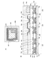
本実施の形態で示す半導体装置を図1に示す。なお、図1(A)は本実施の形態で示す半導体装置の上面構造の一例を示し、図1(A)の断面構造の一部を図1(B)に示している。 A semiconductor device described in this embodiment is illustrated in FIG. Note that FIG. 1A illustrates an example of a top surface structure of the semiconductor device described in this embodiment, and part of the cross-sectional structure in FIG. 1A is illustrated in FIG.
本実施の形態において、半導体装置200は集積回路部201、メモリ部202、アンテナ203を有している(図1(A))。なお、図1(B)において、領域204は図1(A)の集積回路部201の断面構造の一部に対応し、領域205は図1(A)のメモリ部202の断面構造の一部に対応し、領域206は図1(A)のアンテナ203の断面構造の一部に対応している。
In this embodiment mode, the
本実施の形態の半導体装置は、図1(B)に示すように基板778上に絶縁層703を介して設けられた薄膜トランジスタ(TFT)744〜748と、薄膜トランジスタ744〜748上に設けられた絶縁膜750と、当該絶縁膜750上に設けられたソース電極又はドレイン電極として機能する導電膜752〜761とを有する。なお、本実施の形態において、絶縁層703は、接着層を介して基板778上に設けられている。また、本実施の形態において、基板778の材料は特に限定されるものではないが、膜厚が2μm〜20μm程度の基板を用いる。
In the semiconductor device of this embodiment mode, as illustrated in FIG. 1B, thin film transistors (TFTs) 744 to 748 provided over a
また、本実施の形態の半導体装置は、絶縁膜750及び導電膜752〜761上に設けられた絶縁膜762と、絶縁膜762上に設けられた導電膜763〜765と、絶縁膜762及び導電膜763〜765の一部を覆うように設けられた絶縁膜766と、絶縁膜766上に設けられた記憶素子部789、790と、導電膜765上に設けられたアンテナとして機能する導電層786と、絶縁膜766、導電膜771及びアンテナとして機能する導電層786を覆うように設けられた絶縁膜772とを有している。
In addition, the semiconductor device of this embodiment includes the
本実施の形態において絶縁膜772は、好ましくは樹脂(より好ましくはエポキシ樹脂)により形成する。絶縁層772としてエポキシ樹脂を用いることにより、絶縁層772表面の平坦性が向上し、かつ絶縁層772の下層の記憶素子部や素子形成層をほこり等から保護し、かつ半導体装置の機械的強度を保つことが可能である。また、本実施の形態の半導体装置において、アンテナとして機能する導電層を覆う基板として絶縁層772を用いることが可能となるため、薄く湾曲しやすい半導体装置を提供することが可能となる。また、本実施の形態において、アンテナとして機能する導電層786の膜厚に対する該導電層786を覆わない部分の該絶縁層772の膜厚の比の値は少なくとも1.2以上であり、該導電層786の膜厚に対する該導電層786上の該絶縁層772の膜厚の比の値は少なくとも0.2以上であるように、絶縁層772を形成するとよい。そうすることにより、絶縁層772の表面は半導体装置の作製工程において素子形成層への損傷を低減するのに十分な平坦性を有し、また、記憶素子部や素子形成層を保護するために十分な機械的強度を有する半導体装置を得ることが可能となる。なお、図1においてメモリ部および集積回路部はTFTやコンデンサ等の素子を複数有することはいうまでもない。
In this embodiment mode, the insulating
なお、本実施の形態において、半導体装置の側面において導電膜が露出しないように形成するとよい。つまり、半導体装置の側面は、TFTや導電膜を覆う絶縁膜が露出するようにする。そのような構造とすることで、絶縁膜772のみでTFT等の素子やアンテナをほこり等から保護することができ、劣化しずらい半導体装置を提供することが可能となる。
Note that in this embodiment, the conductive film is preferably not exposed on the side surface of the semiconductor device. That is, an insulating film covering the TFT and the conductive film is exposed on the side surface of the semiconductor device. With such a structure, an element such as a TFT and an antenna can be protected from dust and the like only with the insulating
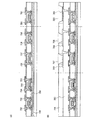
次に、図1に示す半導体装置の作製工程の一例について説明する。 Next, an example of a manufacturing process of the semiconductor device illustrated in FIGS.
まず、第1の基板701の一表面に、剥離層702を形成する(図2(A)参照)。第1の基板701は、絶縁表面を有する。第1の基板701がガラスからなる場合は、その面積や形状に大きな制限はない。そのため、第1の基板701として、例えば、1辺が1メートル以上であって、矩形状のものを用いれば、生産性を格段に向上させることができる。このような利点は、円形の単結晶シリコン基板を用いる場合と比較すると、大きな優位点である。また、基板701がプラスチックからなる場合、作製工程の処理温度に耐えうる耐熱性のプラスチックを用いる必要がある。なお、後述するが、好適には、ガラスからなる第1の基板701上に薄膜トランジスタを設けた後、当該薄膜トランジスタを剥離して、プラスチックからなる基板上に設けてもよい。
First, the
なお、本工程では、剥離層702は、第1の基板701の全面に設けているが、必要に応じて、基板701の全面に剥離層を設けた後に、フォトリソグラフィ法によりパターニングして選択的に設けてもよい。また、第1の基板701に接するように剥離層702を形成しているが、必要に応じて、第1の基板701に接するように下地となる絶縁層を形成し、当該絶縁層に接するように剥離層702を形成してもよい。
Note that in this step, the
剥離層702は、スパッタリング法やプラズマCVD法等により、タングステン(W)、モリブデン(Mo)、チタン(Ti)、タンタル(Ta)、ニオブ(Nb)、ニッケル(Ni)、コバルト(Co)、ジルコニウム(Zr)、亜鉛(Zn)、ルテニウム(Ru)、ロジウム(Rh)、パラジウム(Pd)、オスミウム(Os)、イリジウム(Ir)、珪素(Si)等から選択された元素または前記元素を主成分とする合金材料若しくは化合物材料からなる層を、単層又は積層して形成する。珪素を含む層の結晶構造は、非晶質、微結晶、多結晶のいずれの場合でもよい。
The
次に、剥離層702を覆うように、下地となる絶縁層703を形成する。絶縁層703は、スパッタリング法やプラズマCVD法等により、珪素の酸化物又は珪素の窒化物を含む層を、単層又は積層で形成する。珪素の酸化物材料とは、珪素(Si)と酸素(O)を含む物質であり、酸化珪素、窒素を含む酸化珪素等が該当する。珪素の窒化物材料とは、珪素と窒素(N)を含む物質であり、窒化珪素、酸素を含む窒化珪素等が該当する。下地となる絶縁層は、第1の基板701からの不純物の侵入を防止するブロッキング膜として機能する。
Next, an insulating
次に、絶縁層703上に、非晶質半導体層704を形成する。非晶質半導体層704は、スパッタリング法、LPCVD法、プラズマCVD法等により形成する。続いて、非晶質半導体層704を結晶化法(レーザ結晶化法、RTA又はファーネスアニール炉を用いる熱結晶化法、結晶化を助長する金属元素を用いる熱結晶化法、結晶化を助長する金属元素を用いる熱結晶化法とレーザ結晶化法を組み合わせた方法等)により結晶化して、結晶質半導体層を形成する。その後、得られた結晶質半導体層を所望の形状にパターニングして、結晶質半導体層706〜710を形成する(図2(B)参照)。
Next, an
結晶質半導体層706〜710の作成工程の一例について、以下に説明する。まず、プラズマCVD法を用いて、非晶質半導体層を形成する。次に、結晶化を助長する金属元素であるニッケルを含む溶液を非晶質半導体層上に保持させた後、非晶質半導体層に脱水素化の処理(500℃、1時間)と、熱結晶化の処理(550℃、4時間)を行って結晶質半導体層を形成する。その後、必要に応じてレーザ光を照射し、フォトリソグラフィ法を用いたパターニング処理によって結晶質半導体層706〜710を形成する。
An example of a manufacturing process of the
レーザ結晶化法で結晶質半導体層を形成する場合、気体レーザ又は固体レーザを用いる。気体レーザと固体レーザは、連続発振又はパルス発振のどちらでもよい。例えば、Arレーザ、Krレーザ、エキシマレーザなどの気体レーザ、単結晶のYAG、YVO4、フォルステライト(Mg2SiO4)、YAlO3、GdVO4、若しくは多結晶(セラミック)のYAG、Y2O3、YVO4、YAlO3、GdVO4に、ドーパントとしてNd、Yb、Cr、Ti、Ho、Er、Tm、Taのうち1種または複数種添加されているものを媒質とするレーザ、ガラスレーザ、ルビーレーザ、アレキサンドライトレーザ、Ti:サファイアレーザ、銅蒸気レーザまたは金蒸気レーザのうち一種または複数種から発振されたレーザビームを用いることができる。このようなレーザビームの基本波、及びこれらの基本波の第2高調波から第4高調波のレーザビームを照射することで、大粒径の結晶を得ることができる。 In the case of forming a crystalline semiconductor layer by a laser crystallization method, a gas laser or a solid laser is used. The gas laser and solid-state laser may be either continuous wave or pulsed. For example, gas laser such as Ar laser, Kr laser, excimer laser, single crystal YAG, YVO 4 , forsterite (Mg 2 SiO 4 ), YAlO 3 , GdVO 4 , or polycrystalline (ceramic) YAG, Y 2 O 3 , YVO 4 , YAlO 3 , GdVO 4 with one or more of Nd, Yb, Cr, Ti, Ho, Er, Tm, Ta added as dopants as a medium, laser, glass laser, A laser beam oscillated from one or more of a ruby laser, an alexandrite laser, a Ti: sapphire laser, a copper vapor laser, or a gold vapor laser can be used. By irradiating the fundamental wave of such a laser beam and the second to fourth harmonic laser beams of these fundamental waves, a crystal having a large grain size can be obtained.
なお、単結晶のYAG、YVO4、フォルステライト(Mg2SiO4)、YAlO3、GdVO4、若しくは多結晶(セラミック)のYAG、Y2O3、YVO4、YAlO3、GdVO4に、ドーパントとしてNd、Yb、Cr、Ti、Ho、Er、Tm、Taのうち1種または複数種添加されているものを媒質とするレーザ、Arイオンレーザ、またはTi:サファイアレーザは、連続発振をさせることが可能であり、Qスイッチ動作やモード同期などを行うことによって10MHz以上の発振周波数でパルス発振をさせることも可能である。連続発振レーザ若しくは10MHz以上の周波数で発振するレーザビームを照射することで、結晶化された半導体膜の表面を平坦なものとすることができる。それにより、後の工程で形成するゲート絶縁膜を薄膜化することが可能であり、より薄型の半導体装置を作製することができる。また、ゲート絶縁膜の耐圧を向上させることに寄与することができる。 Note that single crystal YAG, YVO 4 , forsterite (Mg 2 SiO 4 ), YAlO 3 , GdVO 4 , or polycrystalline (ceramic) YAG, Y 2 O 3 , YVO 4 , YAlO 3 , GdVO 4 , dopants Nd, Yb, Cr, Ti, Ho, Er, Tm, Ta, a laser using a medium added with one or more, an Ar ion laser, or a Ti: sapphire laser should oscillate continuously It is also possible to perform pulse oscillation at an oscillation frequency of 10 MHz or more by performing Q switch operation, mode synchronization, or the like. By irradiation with a continuous wave laser or a laser beam oscillated at a frequency of 10 MHz or higher, the surface of the crystallized semiconductor film can be flattened. Accordingly, a gate insulating film formed in a later step can be thinned, and a thinner semiconductor device can be manufactured. Moreover, it can contribute to improving the breakdown voltage of the gate insulating film.
なお、結晶化を助長する金属元素を用いて非晶質半導体層の結晶化を行うと、低温で短時間の結晶化が可能となるうえ、結晶の方向が揃うという利点がある一方、金属元素が結晶質半導体層に残存するためにオフ電流が上昇し、特性が安定しないという欠点がある。そこで、結晶質半導体層上に、ゲッタリングサイトとして機能する非晶質半導体層を形成するとよい。ゲッタリングサイトとなる非晶質半導体層には、リンやアルゴンの不純物元素を含有させる必要があるため、好適には、アルゴンを高濃度に含有させることが可能なスパッタリング法で形成するとよい。その後、加熱処理(RTA法やファーネスアニール炉を用いた熱アニール等)を行って、非晶質半導体層中に金属元素を拡散させ、続いて、当該金属元素を含む非晶質半導体層を除去する。そうすると、結晶質半導体層中の金属元素の含有量を低減又は除去することができる。 Note that when an amorphous semiconductor layer is crystallized using a metal element that promotes crystallization, crystallization can be performed in a short time at a low temperature and the crystal orientation is aligned. Remains in the crystalline semiconductor layer, resulting in an increase in off-current and unstable characteristics. Therefore, an amorphous semiconductor layer functioning as a gettering site is preferably formed over the crystalline semiconductor layer. Since the amorphous semiconductor layer serving as a gettering site needs to contain an impurity element such as phosphorus or argon, it is preferably formed by a sputtering method in which argon can be contained at a high concentration. After that, heat treatment (RTA method or thermal annealing using a furnace annealing furnace) is performed to diffuse the metal element in the amorphous semiconductor layer, and then the amorphous semiconductor layer containing the metal element is removed. To do. Then, the content of the metal element in the crystalline semiconductor layer can be reduced or removed.
次に、結晶質半導体層706〜710を覆うゲート絶縁層705を形成する。ゲート絶縁層705は、プラズマCVD法やスパッタリング法により、珪素の酸化物又は珪素の窒化物を含む層を、単層又は積層して形成する。なお、ゲート絶縁層は、半導体膜706〜710に対し高密度プラズマ処理を行い、表面を酸化又は窒化することで形成しても良い。例えば、He、Ar、Kr、Xeなどの希ガスと、酸素、酸化窒素(NO2)、アンモニア、窒素、水素などの混合ガスを導入したプラズマ処理で形成する。この場合のプラズマの励起は、マイクロ波の導入により行うと、低電子温度で高密度のプラズマを生成することができる。この高密度プラズマで生成された酸素ラジカル(OHラジカルを含む場合もある)や窒素ラジカル(NHラジカルを含む場合もある)によって、半導体膜の表面を酸化又は窒化することができる。
Next, a
このような高密度プラズマを用いた処理により、1〜20nm、代表的には5〜10nmの絶縁膜が半導体膜に形成される。この場合の反応は、固相反応であるため、当該絶縁膜と半導体膜との界面準位密度はきわめて低くすることができる。このような、高密度プラズマ処理は、半導体膜(結晶性シリコン、或いは多結晶シリコン)を直接酸化(若しくは窒化)するため、形成される絶縁膜の厚さは理想的には、ばらつきをきわめて小さくすることができる。加えて、結晶性シリコンの結晶粒界でも酸化が強くされることがないため、非常に好ましい状態となる。すなわち、ここで示す高密度プラズマ処理で半導体膜の表面を固相酸化することにより、結晶粒界において異常に酸化反応をさせることなく、均一性が良く、界面準位密度が低い絶縁膜を形成することができる。よって、より薄く特性のよい半導体装置を作製することが可能である。 By such treatment using high-density plasma, an insulating film with a thickness of 1 to 20 nm, typically 5 to 10 nm, is formed over the semiconductor film. Since the reaction in this case is a solid-phase reaction, the interface state density between the insulating film and the semiconductor film can be extremely low. Such high-density plasma treatment directly oxidizes (or nitrides) a semiconductor film (crystalline silicon or polycrystalline silicon), so that the thickness of the formed insulating film ideally has extremely small variation. can do. In addition, since oxidation is not strengthened even at the crystal grain boundaries of crystalline silicon, a very favorable state is obtained. That is, the surface of the semiconductor film is solid-phase oxidized by the high-density plasma treatment shown here, thereby forming an insulating film with good uniformity and low interface state density without causing an abnormal oxidation reaction at the grain boundaries. can do. Thus, a thinner semiconductor device with favorable characteristics can be manufactured.
ゲート絶縁層は、高密度プラズマ処理によって形成される絶縁膜のみを用いても良いし、それにプラズマや熱反応を利用したCVD法で酸化シリコン、酸窒化シリコン、窒化シリコンなどの絶縁膜を堆積し、積層させても良い。いずれにしても、高密度プラズマで形成した絶縁膜をゲート絶縁層の一部又は全部に含んで形成されるトランジスタは、特性のばらつきを小さくすることができる。よって、より薄く特性のよい半導体装置を作製することが可能である。 As the gate insulating layer, only an insulating film formed by high-density plasma treatment may be used, or an insulating film such as silicon oxide, silicon oxynitride, or silicon nitride is deposited by a CVD method using plasma or thermal reaction. , May be laminated. In any case, variations in characteristics of a transistor formed by including an insulating film formed by high-density plasma in part or all of the gate insulating layer can be reduced. Thus, a thinner semiconductor device with favorable characteristics can be manufactured.
また、半導体膜の結晶化の際に半導体膜に対し、連続発振レーザ若しくは10MHz以上の周波数で発振するレーザビームを照射しながら一方向に走査して結晶化させて得られた半導体膜706〜710は、そのビームの走査方向に結晶が成長する特性がある。その走査方向をチャネル長方向(チャネル形成領域が形成されたときにキャリアが流れる方向)に合わせてトランジスタを配置し、上記ゲート絶縁層を組み合わせることで、特性ばらつきが小さく、しかも電界効果移動度が高いトランジスタ(TFT)を得ることができる。
In addition, when the semiconductor film is crystallized,
次に、ゲート絶縁層705上に、第1の導電層と第2の導電層を積層して形成する。第1の導電層は、プラズマCVD法やスパッタリング法により、20〜100nmの厚さで形成する。第2の導電層は、公知の手段により、100nm〜400nmの厚さで形成する。第1の導電層と第2の導電層は、タンタル(Ta)、タングステン(W)、チタン(Ti)、モリブデン(Mo)、アルミニウム(Al)、銅(Cu)、クロム(Cr)、等から選択された元素又はこれらの元素を主成分とする合金材料若しくは化合物材料で形成する。または、リン等の不純物元素をドーピングした多結晶珪素に代表される半導体材料により形成する。第1の導電層と第2の導電層の組み合わせの例を挙げると、窒化タンタルからなる層とタングステンからなる層、窒化タングステンからなる層とタングステンからなる層、窒化モリブデンからなる層とモリブデンからなる層等が挙げられる。タングステンや窒化タンタルは、耐熱性が高いため、第1の導電層と第2の導電層を形成した後に、熱活性化を目的とした加熱処理を行うことができる。また、2層構造ではなく、3層構造の場合は、モリブデンからなる層とアルミニウムからなる層とモリブデンからなる層の積層構造を採用するとよい。
Next, a first conductive layer and a second conductive layer are stacked over the
次に、フォトリソグラフィ法により、レジストからなるマスクを形成し、ゲート電極とゲート線を形成するためのエッチング処理を行って、ゲート電極として機能する導電層716〜725を形成する。
Next, a resist mask is formed by photolithography, and etching treatment for forming gate electrodes and gate lines is performed, so that
次に、フォトリソグラフィ法により、レジストからなるマスクを形成し、結晶質半導体層706、708〜710に、イオンドープ法又はイオン注入法により、N型を付与する不純物元素を低濃度に添加して、不純物領域711、713〜715とチャネル形成領域780、782〜784を形成する。N型を付与する不純物元素は、15族に属する元素を用いれば良く、例えばリン(P)、砒素(As)を用いる。
Next, a resist mask is formed by photolithography, and an impurity element imparting N-type is added to the crystalline semiconductor layers 706 and 708 to 710 at a low concentration by ion doping or ion implantation.
次に、フォトリソグラフィ法により、レジストからなるマスクを形成し、結晶質半導体層707に、P型を付与する不純物元素を添加して、不純物領域712とチャネル形成領域781を形成する。P型を付与する不純物元素は、例えばボロン(B)を用いる。
Next, a resist mask is formed by photolithography, and an impurity element imparting p-type conductivity is added to the
次に、ゲート絶縁層705と導電層716〜725を覆うように、絶縁層を形成する。絶縁層は、プラズマCVD法やスパッタリング法により、珪素、珪素の酸化物又は珪素の窒化物の無機材料を含む層や、有機樹脂などの有機材料を含む層を、単層又は積層して形成する。次に、絶縁層を垂直方向を主体とした異方性エッチングにより選択的にエッチングして、導電層716〜725の側面に接する絶縁層(サイドウォールともよぶ)739〜743を形成する(図2(C)参照)。また、絶縁層739〜743の作成と同時に、絶縁層705をエッチングして、絶縁層734〜738を形成する。絶縁層739〜743は、後にLDD(Lightly Doped drain)領域を形成する際のドーピング用のマスクとして用いる。
Next, an insulating layer is formed so as to cover the
次に、フォトリソグラフィ法により、レジストからなるマスクを形成し、そのレジストマスクと絶縁層739〜743をマスクとして用いて、結晶質半導体層706、708〜710にN型を付与する不純物元素を添加して、第1の不純物領域(LDD領域ともよぶ)727、729、731、733と、第2の不純物領域726、728、730、732とを形成する。第1の不純物領域727、729、731、733の不純物元素の濃度は、第2の不純物領域726、728、730、732の不純物元素の濃度よりも低い。上記工程を経て、Nチャネル型の薄膜トランジスタ744、746〜748と、Pチャネル型の薄膜トランジスタ745が完成する。
Next, a resist mask is formed by photolithography, and an impurity element imparting N-type is added to the crystalline semiconductor layers 706 and 708 to 710 using the resist mask and the insulating
続いて、薄膜トランジスタ744〜748を覆うように、絶縁層を単層又は積層で形成する(図3(A)参照)。薄膜トランジスタ744〜748を覆う絶縁層は、SOG法、液滴吐出法等により、珪素の酸化物や珪素の窒化物等の無機材料、ポリイミド、ポリアミド、ベンゾシクロブテン、アクリル、エポキシ、シロキサン等の有機材料等により、単層又は積層で形成する。シロキサンとは、Si−O−Si結合を含む樹脂に相当する。シロキサンは、シリコン(Si)と酸素(O)との結合で骨格構造が構成される。置換基として、少なくとも水素を含む有機基(例えばアルキル基、芳香族炭化水素)が用いられる。また、置換基として、フルオロ基を用いてもよい。
Next, an insulating layer is formed as a single layer or a stacked layer so as to cover the
例えば、薄膜トランジスタ744〜748を覆う絶縁層が3層構造の場合、1層目の絶縁層749として酸化珪素を含む層を形成し、2層目の絶縁層750として樹脂を含む層を形成し、3層目の絶縁層751として窒化珪素を含む層を形成するとよい。
For example, when the insulating layer covering the
なお、絶縁層749〜751を形成する前、又は絶縁層749〜751のうちの1つ又は複数を形成した後に、半導体層の結晶性の回復や半導体層に添加された不純物元素の活性化、半導体層の水素化を目的とした加熱処理を行うとよい。加熱処理には、熱アニール、レーザアニール法又はRTA法などを適用するとよい。
Note that before the insulating
次に、フォトリソグラフィ法により、絶縁層749〜751をエッチングして、第2の不純物領域726、728、730、732、不純物領域785を露出させる開口部を形成し、図3(A)に示すように開口部を充填するように、導電層を形成し、当該導電層をパターン加工して、ソース配線又はドレイン配線等として機能する導電層752〜761を形成する。
Next, the insulating
導電層752〜761は、プラズマCVD法やスパッタリング法により、チタン(Ti)、アルミニウム(Al)、ネオジウム(Nd)等から選択された元素、又はこれらの元素を主成分とする合金材料若しくは化合物材料で、単層又は積層で形成する。アルミニウムを主成分とする合金材料とは、例えば、アルミニウムを主成分としニッケルを含む材料、アルミニウムを主成分とし珪素を含む材料、アルミニウムを主成分とし、ニッケル、炭素及び珪素から選択された1種又は複数種とを含む材料に相当する。導電層752〜761は、例えば、バリア層と珪素を含むアルミニウム層とバリア層の積層構造、バリア層と珪素を含むアルミニウム層と窒化チタン層とバリア層の積層構造を採用するとよい。なお、アルミニウムシリコンが含むシリコンは、0.1wt%〜5wt%とする。また、バリア層とは、チタン、チタンの窒化物、モリブデン、又はモリブデンの窒化物からなる薄膜に相当する。アルミニウムや珪素を含むアルミニウムは、抵抗値が低く、安価であるため、導電層752〜761を形成する材料として最適である。また、上層と下層のバリア層を設けると、アルミニウムや珪素を含むアルミニウムのヒロックの発生を防止することができる。また、還元性の高い元素であるチタンからなるバリア層を形成すると、結晶質半導体層上に薄い自然酸化膜ができていたとしても、この自然酸化膜を還元するため、結晶質半導体層とバリア層の接続不良の発生を抑制することができる。
The
次に、導電層752〜761を覆うように、保護膜として機能する絶縁層762を形成する(図3(B)参照)。絶縁膜762は、SOG法、液滴吐出法等を用いて、無機材料又は有機材料(好ましくはエポキシ樹脂)により、単層又は積層で形成する。絶縁層762は、好適には、0.75μm〜3μmの厚さで形成する。
Next, an insulating
続いて、フォトリソグラフィ法により、絶縁層762をエッチングして、導電層757、759、761を露出させる開口部を形成する。続いて、該開口部を充填するように、導電層を形成する。導電層は、プラズマCVD法やスパッタリング法を用いて、導電性材料により形成する。次に、導電層をパターン加工して、導電層757、759、761とそれぞれ電気的に接続する導電層763〜765を形成する。なお、導電層763、764は、記憶素子部が含む一対の導電層のうちの一方の導電層となる。従って、好適には、導電層763〜765は、チタン、又はチタンを主成分とする合金材料若しくは化合物材料により、単層又は積層で形成するとよい。チタンは、抵抗値が低いため、記憶素子部のサイズの縮小につながり、高集積化を実現することができる。また、導電層763〜765を形成するためのフォトリソグラフィ工程においては、下層の薄膜トランジスタ744〜748にダメージを与えないために、ウエットエッチング加工を行うとよく、エッチング剤にはフッ化水素又はアンモニア過水を用いるとよい。
Subsequently, the insulating
次に、導電層763〜765を覆うように、絶縁層766を形成する。絶縁層766は、SOG法、液滴吐出法等を用いて、無機材料又は有機材料により、単層又は積層で形成する。また、絶縁層766は、好適には、0.75μm〜3μmの厚さで形成する。続いて、フォトリソグラフィ法により、絶縁層766をエッチングして、導電層763〜765を露出させる開口部767〜769を形成する。
Next, an insulating
次に、導電層765に接し、アンテナとして機能する導電層786を形成する(図4(A)参照)。導電層786は、プラズマCVD法、スパッタリング法、印刷法、液滴吐出法を用いて、導電性材料により形成する。好ましくは、導電層786は、アルミニウム(Al)、チタン(Ti)、銀(Ag)、銅(Cu)から選択された元素、又はこれらの元素を主成分とする合金材料若しくは化合物材料で、単層又は積層で形成する。具体的には、導電層786は、スパッタリング法によりアルミニウム層を形成し、当該アルミニウム層をパターン加工することにより形成する。アルミニウム層のパターン加工は、ウエットエッチング加工を用いるとよく、ウエットエッチング加工後は200〜300℃の加熱処理を行うとよい。
Next, a
次に、導電層763、764に接するように有機化合物を含む層787を形成する(図4(B)参照)。有機化合物を含む層787は、液滴吐出法や蒸着法等により形成する。続いて、有機化合物を含む層787に接するように、導電層771を形成する。導電層771は、スパッタリング法や蒸着法等により形成する。
Next, a
有機化合物を含む層に用いる有機材料としては、例えば、4、4’−ビス[N−(1−ナフチル)−N−フェニル−アミノ]−ビフェニル(略称:α−NPD)や4,4’−ビス[N−(3−メチルフェニル)−N−フェニル−アミノ]−ビフェニル(略称:TPD)や4,4’,4’’−トリス(N,N−ジフェニル−アミノ)−トリフェニルアミン(略称:TDATA)、4,4’,4’’−トリス[N−(3−メチルフェニル)−N−フェニル−アミノ]−トリフェニルアミン(略称:MTDATA)や4,4’−ビス(N−(4−(N,N−ジ−m−トリルアミノ)フェニル)−N−フェニルアミノ)ビフェニル(略称:DNTPD)などの芳香族アミン系(即ち、ベンゼン環−窒素の結合を有する)の化合物、ポリビニルカルバゾール(略称:PVK)やフタロシアニン(略称:H2Pc)、銅フタロシアニン(略称:CuPc)、バナジルフタロシアニン(略称:VOPc)等のフタロシアニン化合物等を用いることができる。これら材料は、正孔輸送性の高い物質である。 As an organic material used for the layer containing an organic compound, for example, 4,4′-bis [N- (1-naphthyl) -N-phenyl-amino] -biphenyl (abbreviation: α-NPD) or 4,4′- Bis [N- (3-methylphenyl) -N-phenyl-amino] -biphenyl (abbreviation: TPD) or 4,4 ′, 4 ″ -tris (N, N-diphenyl-amino) -triphenylamine (abbreviation) : TDATA), 4,4 ′, 4 ″ -tris [N- (3-methylphenyl) -N-phenyl-amino] -triphenylamine (abbreviation: MTDATA) and 4,4′-bis (N- ( 4- (N, N-di-m-tolylamino) phenyl) -N-phenylamino) biphenyl (abbreviation: DNTPD) and other aromatic amine-based compounds (that is, having a benzene ring-nitrogen bond), polyvinylcarba Z Le (abbreviation: PVK) and phthalocyanine (abbreviation: H2Pc), copper phthalocyanine (abbreviation: CuPc), or vanadyl phthalocyanine (abbreviation: VOPc), and can be used phthalocyanine compounds such as. These materials are substances having a high hole transporting property.
また、他にも有機材料として、例えばトリス(8−キノリノラト)アルミニウム(略称:Alq3)、トリス(4−メチル−8−キノリノラト)アルミニウム(略称:Almq3)、ビス(10−ヒドロキシベンゾ[h]−キノリナト)ベリリウム(略称:BeBq2)、ビス(2−メチル−8−キノリノラト)−4−フェニルフェノラト−アルミニウム(略称:BAlq)等キノリン骨格またはベンゾキノリン骨格を有する金属錯体等からなる材料や、ビス[2−(2−ヒドロキシフェニル)ベンゾオキサゾラト]亜鉛(略称:Zn(BOX)2)、ビス[2−(2−ヒドロキシフェニル)ベンゾチアゾラト]亜鉛(略称:Zn(BTZ)2)などのオキサゾール系、チアゾール系配位子を有する金属錯体などの材料も用いることができる。これら材料は、電子輸送性が高い物質である。 As other organic materials, for example, tris (8-quinolinolato) aluminum (abbreviation: Alq 3 ), tris (4-methyl-8-quinolinolato) aluminum (abbreviation: Almq 3 ), bis (10-hydroxybenzo [h ] -Quinolinato) beryllium (abbreviation: BeBq 2 ), bis (2-methyl-8-quinolinolato) -4-phenylphenolato-aluminum (abbreviation: BAlq), etc. And bis [2- (2-hydroxyphenyl) benzoxazolate] zinc (abbreviation: Zn (BOX) 2 ), bis [2- (2-hydroxyphenyl) benzothiazolate] zinc (abbreviation: Zn (BTZ) 2 ) It is also possible to use materials such as metal complexes having oxazole and thiazole ligands such as it can. These materials are substances having a high electron transporting property.
さらに、金属錯体以外にも、2−(4−ビフェニリル)−5−(4−tert−ブチルフェニル)−1,3,4−オキサジアゾール(略称:PBD)、1,3−ビス[5−(p−tert−ブチルフェニル)−1,3,4−オキサジアゾール−2−イル]ベンゼン(略称:OXD−7)、3−(4−tert−ブチルフェニル)−4−フェニル−5−(4−ビフェニリル)−1,2,4−トリアゾール(略称:TAZ)、3−(4−tert−ブチルフェニル)−4−(4−エチルフェニル)−5−(4−ビフェニリル)−1,2,4−トリアゾール(略称:p−EtTAZ)、バソフェナントロリン(略称:BPhen)、バソキュプロイン(略称:BCP)等の化合物等を用いることができる。 In addition to metal complexes, 2- (4-biphenylyl) -5- (4-tert-butylphenyl) -1,3,4-oxadiazole (abbreviation: PBD), 1,3-bis [5- (P-tert-butylphenyl) -1,3,4-oxadiazol-2-yl] benzene (abbreviation: OXD-7), 3- (4-tert-butylphenyl) -4-phenyl-5- ( 4-biphenylyl) -1,2,4-triazole (abbreviation: TAZ), 3- (4-tert-butylphenyl) -4- (4-ethylphenyl) -5- (4-biphenylyl) -1,2, Compounds such as 4-triazole (abbreviation: p-EtTAZ), bathophenanthroline (abbreviation: BPhen), bathocuproin (abbreviation: BCP), and the like can be used.
またメモリ材料層は単層構造であっても、積層構造であってもよい。積層構造の場合、上記材料から選び、積層構造することができる。また上記有機材料と、発光材料とを積層してもよい。発光材料として、4−ジシアノメチレン−2−メチル−6−(1,1,7,7−テトラメチルジュロリジル−9−エニル)−4H−ピラン(略称:DCJT)、4−ジシアノメチレン−2−t−ブチル−6−(1,1,7,7−テトラメチルジュロリジル−9−エニル)−4H−ピラン、ペリフランテン、2,5−ジシアノ−1,4−ビス(10−メトキシ−1,1,7,7−テトラメチルジュロリジル−9−エニル)ベンゼン、N,N’−ジメチルキナクリドン(略称:DMQd)、クマリン6、クマリン545T、トリス(8−キノリノラト)アルミニウム(略称:Alq3)、9,9’−ビアントリル、9,10−ジフェニルアントラセン(略称:DPA)や9,10−ビス(2−ナフチル)アントラセン(略称:DNA)、2,5,8,11−テトラ−t−ブチルペリレン(略称:TBP)等がある。 The memory material layer may have a single layer structure or a stacked structure. In the case of a laminated structure, a laminated structure can be selected from the above materials. Alternatively, the organic material and the light-emitting material may be stacked. As a light-emitting material, 4-dicyanomethylene-2-methyl-6- (1,1,7,7-tetramethyljulolidyl-9-enyl) -4H-pyran (abbreviation: DCJT), 4-dicyanomethylene-2 -T-butyl-6- (1,1,7,7-tetramethyljulolidyl-9-enyl) -4H-pyran, periflanthene, 2,5-dicyano-1,4-bis (10-methoxy-1) , 1,7,7-tetramethyljulolidyl-9-enyl) benzene, N, N′-dimethylquinacridone (abbreviation: DMQd), coumarin 6, coumarin 545T, tris (8-quinolinolato) aluminum (abbreviation: Alq 3) ), 9,9′-bianthryl, 9,10-diphenylanthracene (abbreviation: DPA), 9,10-bis (2-naphthyl) anthracene (abbreviation: DNA), 2, 5, 8 , 11-tetra-t-butylperylene (abbreviation: TBP).
また、上記発光材料を分散してなる層を用いてもよい。発光材料分散してなる層において、母体となる材料としては、9,10−ジ(2−ナフチル)−2−tert−ブチルアントラセン(略称:t−BuDNA)等のアントラセン誘導体、4,4’−ビス(N−カルバゾリル)ビフェニル(略称:CBP)等のカルバゾール誘導体、ビス[2−(2−ヒドロキシフェニル)ピリジナト]亜鉛(略称:Znpp2)、ビス[2−(2−ヒドロキシフェニル)ベンゾオキサゾラト]亜鉛(略称:ZnBOX)などの金属錯体等を用いることができる。また、トリス(8−キノリノラト)アルミニウム(略称:Alq3)、9,10−ビス(2−ナフチル)アントラセン(略称:DNA)、ビス(2−メチル−8−キノリノラト)−4−フェニルフェノラト−アルミニウム(略称:BAlq)等を用いることができる。 Alternatively, a layer in which the light emitting material is dispersed may be used. In the layer in which the light emitting material is dispersed, the base material includes an anthracene derivative such as 9,10-di (2-naphthyl) -2-tert-butylanthracene (abbreviation: t-BuDNA), 4,4′- Carbazole derivatives such as bis (N-carbazolyl) biphenyl (abbreviation: CBP), bis [2- (2-hydroxyphenyl) pyridinato] zinc (abbreviation: Znpp 2 ), bis [2- (2-hydroxyphenyl) benzoxazola G] A metal complex such as zinc (abbreviation: ZnBOX) can be used. In addition, tris (8-quinolinolato) aluminum (abbreviation: Alq 3 ), 9,10-bis (2-naphthyl) anthracene (abbreviation: DNA), bis (2-methyl-8-quinolinolato) -4-phenylphenolato- Aluminum (abbreviation: BAlq) or the like can be used.
このような有機材料は、熱的作用等によりその性質を変化させるため、ガラス転移温度(Tg)が50℃から300℃、好ましくは80℃から120℃であるとよい。 Such an organic material has a glass transition temperature (Tg) of 50 ° C. to 300 ° C., preferably 80 ° C. to 120 ° C., in order to change its properties by a thermal action or the like.
また、有機材料や発光材料に金属酸化物を混在させた材料を用いてもよい。なお金属酸化物を混在させた材料とは、上記有機材料又は発酵材料と、金属酸化物とが混合した状態、又は積層された状態を含む。具体的には複数の蒸着源を用いた共蒸着法により形成された状態を指す。このような材料を有機無機複合材料と呼ぶことができる。 Alternatively, a material in which a metal oxide is mixed in an organic material or a light emitting material may be used. The material mixed with the metal oxide includes a state where the organic material or fermentation material and the metal oxide are mixed or stacked. Specifically, it refers to a state formed by a co-evaporation method using a plurality of evaporation sources. Such a material can be called an organic-inorganic composite material.
例えば正孔輸送性の高い物質と、金属酸化物を混在させる場合、当該金属酸化物にはバナジウム酸化物、モリブデン酸化物、ニオブ酸化物、レニウム酸化物、タングステン酸化物、ルテニウム酸化物、チタン酸化物、クロム酸化物、ジルコニウム酸化物、ハフニウム酸化物、タンタル酸化物を用いると好ましい。 For example, when a metal oxide is mixed with a substance having a high hole transporting property, the metal oxide includes vanadium oxide, molybdenum oxide, niobium oxide, rhenium oxide, tungsten oxide, ruthenium oxide, titanium oxide. It is preferable to use an oxide, chromium oxide, zirconium oxide, hafnium oxide, or tantalum oxide.
また電子輸送性の高い物質と、金属酸化物を混在させる場合、当該金属酸化物にはリチウム酸化物、カルシウム酸化物、ナトリウム酸化物、カリウム酸化物、マグネシウム酸化物を用いると好ましい。 In the case where a substance having a high electron transporting property and a metal oxide are mixed, it is preferable to use lithium oxide, calcium oxide, sodium oxide, potassium oxide, or magnesium oxide as the metal oxide.
メモリ材料層には、電気的作用、光学的作用又は熱的作用により、その性質が変化する材料を用いればよいため、例えば光を吸収することによって酸を発生する化合物(光酸発生剤)をドープした共役高分子を用いることもできる。共役高分子として、ポリアセチレン類、ポリフェニレンビニレン類、ポリチオフェン類、ポリアニリン類、ポリフェニレンエチニレン類等を用いることができる。また、光酸発生剤としては、アリールスルホニウム塩、アリールヨードニウム塩、o−ニトロベンジルトシレート、アリールスルホン酸p−ニトロベンジルエステル、スルホニルアセトフェノン類、Fe−アレン錯体PF6塩等を用いることができる。 For the memory material layer, a material whose properties are changed by an electric action, an optical action, or a thermal action may be used. For example, a compound that generates an acid by absorbing light (photo acid generator) is used. Doped conjugated polymers can also be used. As the conjugated polymer, polyacetylenes, polyphenylene vinylenes, polythiophenes, polyanilines, polyphenylene ethynylenes, and the like can be used. As the photoacid generator, arylsulfonium salts, aryliodonium salts, o-nitrobenzyl tosylate, arylsulfonic acid p-nitrobenzyl esters, sulfonylacetophenones, Fe-allene complex PF6 salts and the like can be used.
なお、ここでは、記憶素子部789、790として、有機化合物材料を用いた例を示したが、これに限られない。例えば、結晶状態と非晶質状態の間で可逆的に変化する材料や第1の結晶状態と第2の結晶状態の間で可逆的に変化する材料等の相変化材料を用いることができる。また、非晶質状態から結晶状態にのみ変化する材料を用いることも可能である。
Note that here, an example in which an organic compound material is used as the
結晶状態と非晶質状態の間で可逆的に変化する材料とは、ゲルマニウム(Ge)、テルル(Te)、アンチモン(Sb)、硫黄(S)、酸化テルル(TeOx)、Sn(スズ)、金(Au)、ガリウム(Ga)、セレン(Se)、インジウム(In)、タリウム(Tl)、Co(コバルト)及び銀(Ag)から選択された複数を有する材料であり、例えば、Ge−Te−Sb−S、Te−TeO2−Ge−Sn、Te−Ge−Sn−Au、Ge−Te−Sn、Sn−Se−Te、Sb−Se−Te、Sb−Se、Ga−Se−Te、Ga−Se−Te−Ge、In−Se、In−Se−Tl−Co、Ge−Sb−Te、In−Se−Te、Ag−In−Sb−Te系材料が挙げられる。また、第1の結晶状態と第2の結晶状態の間で可逆的に変化する材料とは、銀(Ag)、亜鉛(Zn)、銅(Cu)、アルミニウム(Al)、ニッケル(Ni)、インジウム(In)、アンチモン(Sb)、セレン(Se)及びテルル(Te)から選択された複数を有する材料であり、例えば、Te−TeO2、Te−TeO2−Pd、Sb2Se3/Bi2Te3が挙げられる。この材料の場合、相変化は2つの異なる結晶状態の間で行われる。また、非晶質状態から結晶状態にのみ変化する材料とは、テルル(Te)、酸化テルル(TeOx)、アンチモン(Sb)、セレン(Se)及びビスマス(Bi)から選択された複数を有する材料であり、例えば、Ag−Zn、Cu−Al−Ni、In−Sb、In−Sb−Se、In−Sb−Teが挙げられる。 Materials that reversibly change between a crystalline state and an amorphous state include germanium (Ge), tellurium (Te), antimony (Sb), sulfur (S), tellurium oxide (TeOx), Sn (tin), A material having a plurality of materials selected from gold (Au), gallium (Ga), selenium (Se), indium (In), thallium (Tl), Co (cobalt), and silver (Ag), for example, Ge-Te -Sb-S, Te-TeO 2 -Ge-Sn, Te-Ge-Sn-Au, Ge-Te-Sn, Sn-Se-Te, Sb-Se-Te, Sb-Se, Ga-Se-Te, Ga-Se-Te-Ge, In-Se, In-Se-Tl-Co, Ge-Sb-Te, In-Se-Te, and Ag-In-Sb-Te-based materials can be given. The materials that reversibly change between the first crystal state and the second crystal state are silver (Ag), zinc (Zn), copper (Cu), aluminum (Al), nickel (Ni), A material having a plurality selected from indium (In), antimony (Sb), selenium (Se), and tellurium (Te), for example, Te—TeO 2 , Te—TeO 2 —Pd, Sb 2 Se 3 / Bi. 2 Te 3 is mentioned. In this material, the phase change takes place between two different crystalline states. The material changing only from the amorphous state to the crystalline state is a material having a plurality selected from tellurium (Te), tellurium oxide (TeOx), antimony (Sb), selenium (Se), and bismuth (Bi). Examples thereof include Ag—Zn, Cu—Al—Ni, In—Sb, In—Sb—Se, and In—Sb—Te.
以上の工程を経て、導電層763、有機化合物を含む層787及び導電層771の積層体からなる記憶素子部789と、導電層764、有機化合物を含む層787及び導電層771の積層体からなる記憶素子部790が完成する(図4(B))。
Through the above steps, the
次に、記憶素子部789、790、アンテナとして機能する導電層786を覆うように、保護用の基板として機能する絶縁層772を形成する(図4(B))。絶縁層772は、後に記載する剥離工程においてTFTを含む層への損傷を抑える機能を有する材料であれば特に制限されるものではないが、好ましくは樹脂(より好ましくはエポキシ樹脂)により形成する。絶縁層772としてエポキシ樹脂を用いることにより、絶縁層772表面の平坦性が向上し、後の剥離工程においてTFTを含む層への損傷を低減し、かつ絶縁層772の下層の記憶素子部や素子形成層をほこり等から保護し、半導体装置の機械的強度を保つことが可能である。また、本実施の形態の半導体装置において、アンテナとして機能する導電層786を覆う基板として絶縁層772を用いることができるため、薄く湾曲しやすい半導体装置を提供することが可能となる。なお、本実施の形態において、アンテナとして機能する導電層786の膜厚に対する該導電層786を覆わない部分の該絶縁層772の膜厚の比の値は少なくとも1.2以上であり、該導電層786の膜厚に対する該導電層786上の該絶縁層772の膜厚の比の値は少なくとも0.2以上であるように、絶縁層772を形成するとよい。そうすることにより、絶縁層772の表面は半導体装置の作製工程において素子形成層への損傷を低減するのに十分な平坦性を有し、また、記憶素子部や素子形成層を保護するために十分な機械的強度を有する半導体装置を得ることが可能となる。
Next, an insulating
なお、本実施の形態では、薄膜トランジスタ744〜748、導電層752〜761を含む層を素子形成層791、記憶素子部789、790、アンテナとして機能する導電層786を含む層を領域792とよぶ。また、基板701を除くアンテナとして機能する導電膜786の下層部分の厚さは、5μm以下、好ましくは0.1μm〜3μmの厚さを有するように形成するとよい。なお、ここでは図示しないが、素子形成層791には、メモリ部202、集積回路部201を構成するダイオード、TFT、コンデンサ、抵抗素子などが形成される。
Note that in this embodiment, a layer including the
次に、剥離層702の表面の一部が露出するように、ダイサー、レーザー、ワイヤソーなどにより、絶縁層703、749、750、751、772をエッチングして開口部773、774を形成する(図5(A)参照)。
Next, the insulating
次に、開口部773、774にエッチング剤を導入して、剥離層702を除去する(図5(A)参照)。エッチング剤は、フッ化ハロゲンを含む気体又は液体を使用する。例えば、三フッ化塩素(ClF3)、三フッ化窒素(NF3)、三フッ化臭素(BrF3)、フッ化水素(HF)がある。なお、エッチング剤として、フッ化水素を使用する場合は、剥離層702として、酸化珪素からなる層を用いる。そして、薄膜トランジスタ744〜748を含む層を第1の基板701から剥離する。
Next, an etchant is introduced into the
なお、薄膜トランジスタ744〜748を含む素子形成層791が剥離された第1の基板701は、コストの削減のために、再利用するとよい。また、絶縁層772は、剥離層702を除去した後に、素子形成層791が飛散しないように設けたものである。素子形成層791は小さく薄く軽いために、剥離層702を除去した後は、第1の基板701に密着していないために飛散しやすい。しかしながら、素子形成層791上に絶縁層772を形成することで、素子形成層791に重みが付き、第1の基板701からの飛散を防止することができる。また、素子形成層791単体では薄くて軽いが、絶縁層772を形成することで、巻かれた形状になることがなく、ある程度の強度を確保することができる。
Note that the
次に、絶縁層772をシート材776に接着させて、第1の基板701から完全に剥離する(図4(B)参照)。ここで、シート材776は、通常の状態ではその接着力が強く、熱を加えたり、光を照射することによりその接着力が弱くなる性質を有するものを用いるとよい。例えば、加熱することにより接着力が弱くなる熱剥離テープや、紫外光を照射することにより接着力が弱くなるUV剥離テープ等を用いるとよい。また、通常の状態で接着力が弱い弱粘性テープ等を用いてもよい。
Next, the insulating
次に、絶縁層703上に第2の基板778を固定する。ここで、第2の基板778は、ポリプロピレン、ポリエステル、ビニル、ポリフッ化ビニル、塩化ビニルなどからなるフィルム、繊維質な材料からなる紙、基材フィルム(ポリエステル、ポリアミド、無機蒸着フィルム、紙類等)と接着性合成樹脂フィルム(アクリル系合成樹脂、エポキシ系合成樹脂等)との積層フィルムなどを用いることができる。なお、第2の基板778は膜厚が2μm以上20μ以下程度であることが好ましい。第2の基板778がプラスチックからなる場合、薄型、軽量で、曲げることが可能であるためデザイン性に優れ、フレキシブルな形状への加工が容易である。また、耐衝撃性に優れ、様々な物品に貼り付けたり、埋め込んだりすることが容易であり、多種多様な分野で活用することができる。
Next, the
また、本実施の形態において、第2の基板778の絶縁層703側の表面には接着層が設けられている。接着層は、熱硬化樹脂、紫外線硬化樹脂、酢酸ビニル樹脂系接着剤、ビニル共重合樹脂系接着剤、エポキシ樹脂系接着剤、ウレタン樹脂系接着剤、ゴム系接着剤、アクリル樹脂系接着剤等の接着剤を含む層に相当する。
In this embodiment, an adhesive layer is provided on the surface of the
また、本実施の形態において、第2の基板778の絶縁層703側ではない表面に第2の基板778よりも膜厚が厚い支持体779を有する。本実施の形態において、第2の基板778は、2μm〜20μm程度と薄いため取り扱いが困難であるが、支持体779を有することにより第2の基板778の取り扱いが容易となる。なお、支持体779は工程の最後に除去される。本実施の形態において、第2の基板778が支持体779を有することによって、第2の基板778として非常に膜厚の薄いものを用いることが可能となった。
In this embodiment, the
なお、第2の基板778の表面は、二酸化珪素(シリカ)の粉末により、コーティングされていてもよい。コーティングにより、高温で高湿度の環境下においても防水性を保つことができる。また、その表面は、インジウム錫酸化物等の導電性材料によりコーティングされていてもよい。コーティングした材料が静電気をチャージし、薄膜集積回路を静電気から保護することができる。また、その表面は、炭素を主成分とする材料(例えば、ダイヤモンドライクカーボン)によりコーティングされていてもよい。コーティングにより強度が増し、半導体装置の劣化や破壊を抑制することができる。
Note that the surface of the
次に、素子形成層791を有する基板778とシート材776とを分離する。ここでは、シート材776としてUV剥離テープを用いる場合を説明する。まず、シート材776と絶縁層772との接着力を弱めるためにシート材776に紫外光を照射する(図6(A))。次に、シート材776を絶縁層772から分離する。続いて、第2の基板778に設けられた支持体779を第2の基板778から分離する。
Next, the
以上の工程により、図1(B)に示すような半導体装置を作製することができる。 Through the above steps, a semiconductor device as illustrated in FIG. 1B can be manufactured.
なお、図1においてアンテナ203は、メモリ部202に対して、重なるように設けてもよいし、重ならずに周囲に設ける構造でもよい。また重なる場合も全面が重なってもよいし、一部が重なっている構造でもよい。
Note that in FIG. 1, the
半導体装置200の無線による信号の伝送方式は、電磁結合方式、電磁誘導方式またはマイクロ波方式等を用いることができる。伝送方式は、実施者が使用用途を考慮して適宜選択すればよく、伝送方式に伴って最適なアンテナを設ければよい。
As a wireless signal transmission method of the
電磁結合方式または電磁誘導方式(例えば13.56MHz帯)を用いる場合には、磁界密度の変化による電磁誘導を利用するため、アンテナとして機能する導電層を輪状(例えば、ループアンテナ)、らせん状(例えば、スパイラルアンテナ)に形成する。 In the case of using an electromagnetic coupling method or an electromagnetic induction method (for example, 13.56 MHz band), a conductive layer functioning as an antenna is formed in a ring shape (for example, a loop antenna) or a spiral shape (for example, a loop antenna) in order to use electromagnetic induction due to a change in magnetic field density. For example, a spiral antenna is formed.
また、マイクロ波方式(例えば、UHF帯(860〜960MHz帯)、2.45GHz帯等)を用いる場合には、信号の伝送に用いる電磁波の波長を考慮してアンテナとして機能する導電層の長さ等の形状を適宜設定すればよい。例えば、アンテナとして機能する導電層を線状(例えば、ダイポールアンテナ)、平坦な形状(例えば、パッチアンテナ)またはリボン型の形状に形成することができる。アンテナとして機能する導電層の形状は線状に限られず、電磁波の波長を考慮して曲線状や蛇行形状またはこれらを組み合わせた形状で設けてもよい。 In the case of using a microwave method (for example, UHF band (860 to 960 MHz band), 2.45 GHz band, or the like), the length of the conductive layer functioning as an antenna in consideration of the wavelength of an electromagnetic wave used for signal transmission. Such a shape may be set as appropriate. For example, the conductive layer functioning as an antenna can be formed into a linear shape (for example, a dipole antenna), a flat shape (for example, a patch antenna), or a ribbon shape. The shape of the conductive layer that functions as an antenna is not limited to a linear shape, and may be provided in a curved shape, a meandering shape, or a combination thereof in consideration of the wavelength of electromagnetic waves.
また、TFTはチャネル形成領域が一つ形成されるシングルゲート構造でもよいし、二つ形成されるダブルゲート構造または三つ形成されるトリプルゲート構造であってもよい。つまり、チャネル形成領域を複数有するマルチゲート構造のTFTにも適用することができる。また、周辺駆動回路領域の薄膜トランジスタも、シングルゲート構造、ダブルゲート構造またはトリプルゲート構造などのマルチゲート構造であってもよい。 The TFT may have a single gate structure in which one channel formation region is formed, a double gate structure in which two channel formation regions are formed, or a triple gate structure in which three channel formation regions are formed. That is, it can be applied to a multi-gate TFT having a plurality of channel formation regions. The thin film transistor in the peripheral driver circuit region may also have a multi-gate structure such as a single gate structure, a double gate structure, or a triple gate structure.
また、本実施の形態で示したTFTの作製方法に限らず、トップゲート型(プレーナー型)、ボトムゲート型(逆スタガ型)、あるいはチャネル領域の上下にゲート絶縁膜を介して配置された2つのゲート電極を有する、デュアルゲート型やその他の構造においても本発明を適用することができる。 In addition to the TFT manufacturing method described in this embodiment mode, a top gate type (planar type), a bottom gate type (inverse stagger type), or 2 arranged above and below a channel region with a gate insulating film interposed therebetween. The present invention can also be applied to a dual gate type or other structure having two gate electrodes.
本発明の半導体装置は、少なくとも片面を樹脂により覆われているため、樹脂層の下層の記憶素子部や素子形成層をほこり等から保護し、かつ半導体装置の機械的強度を保つことが可能である。また、本発明の半導体装置において、少なくとも片面を覆う基板として樹脂層を用いるため、薄く湾曲しやすい半導体装置を提供することが可能となる。また、アンテナとして機能する導電層の膜厚に対する該導電層を覆わない部分の該絶縁層の膜厚の比の値は少なくとも1.2以上であり、該導電層の膜厚に対する該導電層上の該絶縁層の膜厚の比の値は少なくとも0.2以上であるように、該導電層上に該絶縁層を形成するため、該絶縁層の表面は半導体装置の作製工程において素子形成層への損傷を低減するのに十分な平坦性を有し、また、記憶素子部や素子形成層を保護するために十分な機械的強度を有する半導体装置を得ることが可能となる。また、本発明の半導体装置は、半導体装置の側面において導電膜が露出せず、TFTや導電膜を覆う絶縁膜が露出するように形成してもよい。それにより、アンテナとして機能する導電膜を覆う絶縁層のみでTFT等の素子やアンテナをほこり等から保護することができ、劣化しずらい半導体装置を提供することが可能となる。また、本発明の半導体装置において素子形成層側を覆う基板として、作製工程において表面に支持体を有する基板を用いるため、2μm以上20μm以下程度の基板を容易に取り扱うことができる。よって、薄く湾曲しやすい半導体装置を容易に作製することが可能となる。 Since at least one surface of the semiconductor device of the present invention is covered with resin, it is possible to protect the memory element portion and the element formation layer below the resin layer from dust and the like and to maintain the mechanical strength of the semiconductor device. is there. In the semiconductor device of the present invention, since a resin layer is used as a substrate covering at least one surface, a thin and easily bent semiconductor device can be provided. The ratio of the thickness of the insulating layer in the portion not covering the conductive layer to the thickness of the conductive layer functioning as an antenna is at least 1.2 or more. In order to form the insulating layer on the conductive layer so that the value of the ratio of the thickness of the insulating layer is at least 0.2 or more, the surface of the insulating layer is an element formation layer in the manufacturing process of the semiconductor device. It is possible to obtain a semiconductor device having flatness sufficient to reduce damage to the semiconductor device and sufficient mechanical strength to protect the memory element portion and the element formation layer. Further, the semiconductor device of the present invention may be formed so that the conductive film is not exposed on the side surface of the semiconductor device, and the insulating film covering the TFT and the conductive film is exposed. Accordingly, an element such as a TFT and an antenna can be protected from dust and the like only with an insulating layer covering a conductive film functioning as an antenna, and a semiconductor device that is difficult to deteriorate can be provided. In addition, since a substrate having a support on the surface is used in the manufacturing process as the substrate covering the element formation layer side in the semiconductor device of the present invention, a substrate having a thickness of about 2 μm to 20 μm can be easily handled. Accordingly, a thin and easily bent semiconductor device can be easily manufactured.
(実施の形態2)
本実施の形態において、実施の形態1と異なる半導体装置の作製工程について説明する。具体的には、メモリセルのpn接合と該メモリセルを制御するロジック部の薄膜トランジスタとを同時に形成する工程について説明する。
(Embodiment 2)
In this embodiment mode, a manufacturing process of a semiconductor device which is different from that in
図7に、本実施の形態の半導体装置の模式的な断面構造を示す。本実施の形態の半導体装置は、アンテナ、メモリ部、集積回路部を有している。図7において、図面の真ん中の領域にメモリ部の一部としてダイオード上に記憶素子部が積層されたメモリセルの断面を示す。また、図面の左側の領域にメモリ部のロジック回路の断面の一部として、pチャネル型TFT(「pch−TFT」とも表記する。)、nチャネル型TFT(「Nch−TFT」とも表記する。)の断面を示す。また、図面の右側の領域にアンテナの一部の断面と共に、集積回路部の断面の一部として、共振回路212のコンデンサ、電源回路213の高耐圧型のnチャネル型TFTを示す。なお、集積回路部にも、高耐圧型のTFTの他、図面の左側のロジック回路と同様のpチャネル型TFTおよびnチャネル型TFTが形成されることはいうまでもない。また、メモリ部および集積回路部は、図7に図示されたTFTやコンデンサを複数有することはいうまでもない。
FIG. 7 shows a schematic cross-sectional structure of the semiconductor device of this embodiment. The semiconductor device of this embodiment includes an antenna, a memory portion, and an integrated circuit portion. 7 shows a cross section of a memory cell in which a memory element portion is stacked on a diode as a part of the memory portion in a middle region of the drawing. In addition, a p-channel TFT (also referred to as “pch-TFT”) and an n-channel TFT (“Nch-TFT”) are also illustrated as part of the cross section of the logic circuit in the memory portion in the left region of the drawing. ) Is shown. In addition, in the region on the right side of the drawing, a capacitor of the
次に、基板260は素子形成層250を製造するときに使用される基板である。本実施例ではガラス基板を用いる。基板260上には、素子形成層250から基板260を除去するために用いる剥離層261が形成されている。基板260上に剥離層261を形成してから、下地絶縁層249を形成し、下地絶縁層249上にTFTななどでなる素子形成層250を形成する。以下、図7〜図11を用いて本実施の形態の半導体装置の形成方法を説明する。
Next, the
基板260にガラス基板260を用いる。図8(S1)に示すように、基板260上に3層261a〜261cでなる剥離層261を形成する。第1層261aは、平行平板型プラズマCVD装置により、原料ガスにSiH4、N2Oを用いて酸化窒化シリコン膜(SiOxNy、x>y)を厚さ100nm形成する。第2層261bとして、厚さ30nmのタングステン膜をスパッタリング装置で成膜する。第3層261cとして、厚さ200nmの酸化シリコン膜をスパッタリング装置で成膜する。
A
第3層261c(酸化シリコン)を成膜することで、第2層261b(タングステン)の表面が酸化され、界面にタングステン酸化物が形成される。タングステン酸化物が形成されることで、のちに素子形成層250を他の基板に転載するときに、基板260を分離しやすくなる。第1層261aは、素子形成層250を作製している間、第2層261bの密着性を維持するための層である。
By depositing the
第2層261bには、タングステン(W)他、モリブデン(MO)、チタン(Ti)、タンタル(Ta)、ニオブ(Nb)、ニッケル(Ni)、コバルト(CO)、ジルコニウム(Zr)、亜鉛(ZN)、ルテニウム(Ru)、ロジウム(Rh)、パラジウム(Pd)、オスミウム(Os)、イリジウム(Ir)の金属膜や、これらの金属の化合物が好ましい。また、第2層261bの厚さは20nm以上40nm以下とすることができる。
The
図8(S2)に示すように、剥離層261上に、2層構造の下地絶縁層249を形成する。第1層249aとして、プラズマCVD装置により原料ガスにSiH4、N2O、NH3、H2を用いて酸化窒化シリコン(SiOxNy、x<y)を厚さ50nm形成する。第1層249aの窒素の組成比が40%以上となるようにしてバリア性を高めた。第2層249bは、プラズマCVD装置によりSiH4、N2Oを原料ガスに用いて、酸化窒化シリコン(SiOxNy、x>y)を厚さ100nm成膜する。第2層249bの窒素の組成比は0.5%以下とする。
As illustrated in FIG. 8 (S2), a
図8(S3)に示すように、下地絶縁層249上に、結晶性シリコン膜271を形成する。結晶性シリコン膜271は次の方法で作製する。プラズマCVD装置により、原料ガスにSiH4およびH2を用い、厚さ66nmの非晶質シリコン膜を形成する。非晶質シリコン膜にレーザを照射して結晶化させることで、結晶性シリコン膜271とする。レーザ照射方法の一例を示す。LD励起のYVO4レーザの第2高調波(波長532nm)を照射する。特に第2高調波に限定する必要はないが、第2高調波はエネルギー効率の点で3次以上の高次の高調波より優れている。照射面において、光学系によりビームの形状が長さ500μm、幅20μm程度の線状となるように、またその強度が10〜20Wとなるようにする。またビームを基板に対して相対的に10〜50cm/secの速度で移動する。
As shown in FIG. 8 (S3), a
図8(S4)に示すように、結晶性シリコン膜271にp型不純物を添加する。ここでは、イオンドーピング装置において、ドーピングガスに水素で希釈したジボラン(B2H6)を用い、ボロンを結晶性シリコン膜271の全体に添加する。非晶質シリコンを結晶化した結晶性シリコンは不対結合を有するため、理想的な真性シリコンではなく、弱いn型の導電性を示す。そのため、p型不純物を微量添加することにより、結晶性シリコン膜271が真性シリコンとなるようにする効果がある。図8(S4)の工程は必要に応じて行えばよい。
As shown in FIG. 8 (S 4), a p-type impurity is added to the
図8(S5)に示すように、結晶性シリコン膜271を素子ごとに分割し、半導体層272〜276を形成する。半導体層272にメモリセルのダイオードが形成される。半導体層273〜275は、それぞれ、TFTのチャネル形成領域、ソース領域およびドレイン領域が形成される。半導体層276はMIS型コンデンサの電極を構成する。結晶性シリコン膜271を加工する方法の一例を示す。フォトリソグラフィ工程によりレジストを結晶性シリコン膜271上に形成し、レジストをマスクにして、ドライエッチング装置により、エッチング剤にSF6、O2を用いて結晶性シリコン膜271をエッチングすることで、所定の形状の半導体層272〜276を形成する。
As shown in FIG. 8 (S5), the
図9(S6)に示すように、フォトリソグラフィ工程によりレジスRト31を形成し、nチャネル型TFTの半導体層274および275にp型不純物を微量添加する。ここでは、ドーピングガスに水素で希釈したジボラン(B2H6)を用い、イオンドーピング装置により半導体層274、275にボロンをドーピングする。ドーピングが終了したらレジストR31を除去する。 As shown in FIG. 9 (S6), a resist R 31 is formed by a photolithography process, and a small amount of p-type impurity is added to the semiconductor layers 274 and 275 of the n-channel TFT. Here, diborane (B 2 H 6 ) diluted with hydrogen is used as a doping gas, and boron is doped into the semiconductor layers 274 and 275 with an ion doping apparatus. When the doping is completed, the resist R31 is removed.
図9(S6)の工程は、nチャネル型TFTのしきい値電圧が負の電圧にならないようすることを目的とする。nチャネル型TFTの半導体層274、275に5×10¹⁵atoms/cm3以上1×1017atoms/cm3以下の濃度でボロンを添加すればよい。図9(S6)の工程は必要に応じて行えばよい。また、メモリセルの半導体層272にp型不純物を添加してもよい。
The step of FIG. 9 (S6) aims to prevent the threshold voltage of the n-channel TFT from becoming a negative voltage. Boron may be added to the semiconductor layers 274 and 275 of the n-channel TFT at a concentration of 5 × 10 15 atoms /
図9(S7)に示すように、基板260全体に絶縁膜277を形成する。絶縁膜277はTFTのゲート絶縁膜、コンデンサの誘電体となる。ここでは、プラズマCVD装置により、プラズマCVD装置により原料ガスSiH4、N2Oを用いて酸化窒化シリコン膜(SiOxNy、x>y)を厚さ20〜40nm程度で形成する。
As shown in FIG. 9 (S7), an insulating
図9(S8)に示すように、フォトリソグラフィ工程によりレジストR32を形成し、メモリセルの半導体層272およびコンデンサの半導体層276にn型不純物を添加する。この工程により、半導体層272のn型不純物領域とコンデンサの一方の電極として機能するn型不純物領域のn型不純物の濃度が決定される。ドーピングガスに水素で希釈したホスフィン(PH3)を用いて、イオンドーピング装置により半導体層272、276にリンをドーピングする。よって、半導体層272全体がn型不純物領域278となり、半導体層276全体がn型不純物領域279となる。ドーピング工程が終了したら、レジストR32を除去する。
As shown in FIG. 9 (S8), a resist R32 is formed by a photolithography process, and an n-type impurity is added to the
図9(S9)に示すように、絶縁膜277上に導電膜281を形成する。導電膜281は、TFTのゲート電極などを構成する。ここでは、導電膜281を2層の多層構造とする。1層目は厚さ30nmのタンタル窒化物(TaN)、2層目は厚さ370nmのタングステン(W)とする。タンタル窒化物、タングステンはそれぞれスパッタリング装置で成膜する。
As shown in FIG. 9 (S9), a
導電膜281上にフォトリソグラフィ工程によりレジストを形成し、エッチング装置により導電膜281をエッチングして、図10(S10)に示すように、第1導電膜283〜285を半導体層273〜275上に形成する。第1導電膜283〜285はTFTのゲート電極またはゲート配線となる。高耐圧型のnチャネル型TFTでは、他のTFTよりもゲート幅(チャネル長)が広くなるように、導電膜285を形成している。第1導電膜286はコンデンサの一方の電極を構成する。
A resist is formed over the
導電膜281はドライエッチング法によりエッチングする。エッチング装置にICP(Inductively Coupled Plasma:誘導結合型プラズマ)エッチング装置法を用いる。エッチング剤としては、はじめにタングステンをエッチングするためCl2、SF6、O2の混合ガスを用い、つぎに、処理室に導入するエッチング剤をCl2ガスのみに変更し、タンタル窒化物をエッチングする。
The
図10(S11)に示すように、フォトリソグラフィ工程によりレジストR33を形成する。nチャネル型TFTの半導体層274と275にn型不純物を添加する。第1導電膜284がマスクとなり半導体層274にn型低濃度不純物領域288、289が自己整合的に形成され、第1導電膜285がマスクとなり半導体層275にn型低濃度不純物領域290、291が自己整合的に形成される。本実施例では、水素で希釈したホスフィン(PH3)をドーピングガスに用い、イオンドーピング装置により半導体層274、275にリンを添加する。図10(S11)の工程は、nチャネル型TFTにLDD領域を形成するための工程である。n型低濃度不純物領域288、289のn型不純物が、1×10¹⁶atoms/cm3以上5×1018atoms/cm3以下の範囲で含まれるようにする。
As shown in FIG. 10 (S11), a resist R33 is formed by a photolithography process. An n-type impurity is added to the semiconductor layers 274 and 275 of the n-channel TFT. The n-type low
図10(S12)に示すように、フォトリソグラフィ工程によりレジストR34を形成する。メモリセルの半導体層272、およびpチャネル型TFTの半導体層273にp型不純物を添加する。半導体層272は、n型不純物領域272nとして残す部分がレジストR34に覆われているため、露出している領域272pがp型不純物領域となる。この不純物添加工程により、半導体層272には、pn接合を構成するn型不純物領域272nとp型不純物領域272pが形成される。半導体層272は予めn型不純物領域278とされているため、領域272pがp型の導電性を示すように、予め添加されているn型不純物よりも高濃度にp型不純物を添加する。
As shown in FIG. 10 (S12), a resist R34 is formed by a photolithography process. A p-type impurity is added to the
第1導電膜283がマスクとなり半導体層273にp型高濃度不純物領域273a、273bが自己整合的に形成される。また第1導電膜283で覆われている領域273cがチャネル形成領域として自己整合的に形成される。
Using the first
p型不純物領域の添加は、ドーピングガスに水素で希釈したジボラン(B2H6)を用いて、イオンドーピング装置により半導体層274、275にボロンをドーピングする。ドーピングが終了したらレジストR34を除去する。 The p-type impurity region is added by doping boron into the semiconductor layers 274 and 275 with an ion doping apparatus using diborane (B 2 H 6 ) diluted with hydrogen as a doping gas. When the doping is completed, the resist R34 is removed.
図10(S13)に示すように、第1導電膜283〜285の周囲に絶縁層293〜296を形成する。絶縁層293〜295はサイドウォール、側壁と呼ばれるものである。まず、原料ガスにSiH4、N2Oを用いて、プラズマCVD装置により酸化窒化シリコン膜(SiOxNy、x>y)を100nmの厚さに形成する。次に、原料ガスにSiH4、N2Oを用いて、LPCVD装置により酸化シリコン膜を200nmの厚さに形成する。フォトリソグラフィ工程によりレジスト形成する。このレジストを用いて、まず、上層の酸化シリコン膜をバッファードフッ酸でウェットエッチング処理する。次に、レジストを除去し、下層の窒化酸化シリコン膜ドライエッチング処理をすることで、絶縁層293〜296が形成される。この一連の工程で、酸化窒化シリコンでなる絶縁膜277もエッチングされ、絶縁膜277は第1導電膜283〜285と絶縁層293〜296の下部のみ残る。
As shown in FIG. 10 (S13), insulating layers 293-296 are formed around the first conductive films 283-285. The insulating
図11(S14)に示すように、フォトリソグラフィ工程によりレジストR35を形成する。nチャネル型TFTの半導体層274、275とコンデンサの半導体層にn型不純物を添加し、n型高濃度不純物領域を形成する。半導体層274は、第1導電膜284、絶縁層294がマスクとなり、n型低濃度不純物領域288、299(図10(S11)参照)にさらにn型不純物が添加され、n型高濃度不純物領域274a、274bが自己整合的に形成される。第1導電膜284と重なる領域274cがチャネル形成領域として自己整合的に確定する。また、n型低濃度不純物領域288、299において絶縁層294と重なる領域274e、274dは、そのままn型低濃度不純物領域として確定する。
As shown in FIG. 11 (S14), a resist R35 is formed by a photolithography process. An n-type impurity is added to the semiconductor layers 274 and 275 of the n-channel TFT and the semiconductor layer of the capacitor to form an n-type high concentration impurity region. In the
半導体層275も半導体層274と同様、n型高濃度不純物領域275a、275b、チャネル形成領域275c、n型低濃度不純物領域275e、275dが形成される。
Similarly to the
このとき、半導体層276全体はn型不純物領域279が形成されている(図9(S8)参照)。第1導電膜286および絶縁層296がマスクとなり、n型不純物領域279にさらにn型不純物が添加され、n型高濃度不純物領域276a、276bが自己整合的に形成される。半導体層276の第1導電膜286および絶縁層296と重なる領域がn型不純物領域276cとして確定する。
At this time, an n-
n型不純物の添加工程は、上述したとおり、イオンドーピング装置を使用し、ドーピングガスに水素で希釈したホスフィン(PH3)を用いればよい。nチャネル型TFTのn型高濃度不純物領域274a、274b、275a、275bには、リンの濃度が1×10²⁰atoms/cm3以上2×1021atoms/cm3以下の範囲になるように、リンがドーピングされる。
As described above, the n-type impurity addition step may be performed by using an ion doping apparatus and using phosphine (PH 3 ) diluted with hydrogen as a doping gas. In the n-type high-
上述したように、本実施形態では、薄膜トランジスタおよびコンデンサの半導体膜に不純物を添加する一連の工程において、メモリセルのn型不純物領域272n、p型不純物領域272pが形成される。本実施形態では、n型不純物領域272nとコンデンサのn型不純物領域276cとは、n型不純物およびp型不純物の濃度が同じになる。よって、同じシート抵抗を示すこととなる。p型不純物領域272pは、pチャネル型薄膜トランジスタのp型高濃度不純物領域273a、273bとp型不純物の濃度が同じになるが、n型不純物の濃度は高い。また、p型不純物領域272pは、コンデンサのn型不純物領域276cとn型不純物の濃度が同じになる。
As described above, in this embodiment, the n-
レジストR35を除去し、図11(S15)に示すように、キャップ絶縁膜298を形成する。キャップ絶縁膜298として、プラズマCVD装置により、プラズマCVD装置により酸化窒化シリコン膜(SiOxNy、x>y)を50nmの厚さに形成する。酸化窒化シリコン膜の原料ガスには、SiH4、N2Oを用いる。キャップ絶縁膜298を成膜した後、窒素雰囲気中で550℃の加熱処理を行い、半導体層272〜276に添加したn型不純物およびp型不純物を活性化する。
The resist R35 is removed, and a
図11(S16)に示すように、第1層間絶縁膜299、300を形成する。1層目の第1層間絶縁膜299として、プラズマCVD装置により原料ガスにSiH4、N2Oを用いて、酸化窒化シリコン(SiOxNy、x<y)を100nmの厚さに形成する。2層目の第1層間絶縁膜300には、プラズマCVD装置により原料ガスにSiH4、N2O、NH3、H2を用いて、酸化窒化シリコン(SiOxNy、x>y)を600nmの厚さに形成する。
As shown in FIG. 11 (S16), first
フォトリソグラフィ工程とドライエッチング工程により、第1層間絶縁膜299、300およびキャップ絶縁膜298を除去し、コンタクトホールを形成する。第1層間絶縁膜300上に導電膜を形成する。ここでは、導電膜を4層構造とする。下から、厚さ60nmのTi、40nmのTiN、500nmの純アルミニウム、100nmのTiNの順に積層する。それぞれの層はスパッタリング装置で成膜する。フォトリソグラフィ工程とドライエッチング工程により導電膜を所定の形状に加工し、第2導電膜301〜314を形成する。
The first
なお、第2導電膜と第1導電膜が接続されることを説明するため、図面では、第2導電膜と第1導電膜が半導体層上で接続するように示しているが、実際には、第2導電膜と第1導電膜とのコンタクト部分は半導体層上をさけて形成されている。 Note that, in order to explain that the second conductive film and the first conductive film are connected, the drawing shows that the second conductive film and the first conductive film are connected on the semiconductor layer. The contact portion between the second conductive film and the first conductive film is formed on the semiconductor layer.
メモリセルの第2導電膜301はワード線を形成する。第2導電膜302はダイオードと記憶素子を接続するための電極であり、メモリセルごとに分割されている。第2導電膜312によりn型高濃度不純物領域276aと276bが接続されている。よって、n型不純物領域276c、絶縁膜277、第1導電膜296でなる積層構造のMIS型コンデンサが形成される。第2導電膜314は集積回路部240の端子であり、アンテナ210が接続される。
The second
続いて、実施の形態1と同様の工程を経ることにより、図7に示すような半導体装置を得ることができる。つまり、第2の導電膜301〜314上に絶縁層762が形成され、絶縁膜762上にコンタクトホールを介して導電層764、765が形成され導電層764、765上に絶縁層762が形成され、絶縁層762及び導電層764の一部を覆うように有機化合物を含む層787が形成され、有機化合物を含む層787上に導電層771が形成され、導電層765上にアンテナとして機能する導電層786が形成され、導電層771及び導電層786上に絶縁層772が形成された構造を得ることができる。
Subsequently, a semiconductor device as shown in FIG. 7 can be obtained through the same steps as in the first embodiment. That is, the insulating
なお、コンデンサの半導体層276の不純物領域をn型としたが、p型とすることもできる。この場合、図9(S8)の工程でp型の不純物領域を添加する。図9(S8)の工程でメモリセルの半導体層272全体がp型不純物領域とされる。そのため、図10(S12)の工程で、半導体層272にp型不純物を添加しない。そして図11(S14)の工程で半導体層272の所定の領域にn型不純物を添加する。
Although the impurity region of the
本発明の半導体装置は、少なくとも片面を樹脂により覆われているため、樹脂層の下層の記憶素子部や素子形成層をほこり等から保護し、かつ半導体装置の機械的強度を保つことが可能である。また、本発明の半導体装置において、少なくとも片面を覆う基板として樹脂層を用いるため、薄く湾曲しやすい半導体装置を提供することが可能となる。また、アンテナとして機能する導電層の膜厚に対する該導電層を覆わない部分の絶縁層の膜厚の比の値は少なくとも1.2以上であり、該導電層の膜厚に対する該導電層上の該絶縁層の膜厚の比の値は少なくとも0.2以上であるように、該導電層上に該絶縁層を形成するため、該絶縁層の表面は半導体装置の作製工程において素子形成層への損傷を低減するのに十分な平坦性を有し、また、記憶素子部や素子形成層を保護するために十分な機械的強度を有する半導体装置を得ることが可能となる。また、本発明の半導体装置は、半導体装置の側面において導電膜が露出せず、TFTや導電膜を覆う絶縁膜が露出するように形成してもよい。それにより、アンテナとして機能する導電膜を覆う絶縁層のみでTFT等の素子やアンテナをほこり等から保護することができ、劣化しずらい半導体装置を提供することが可能となる。また、本発明の半導体装置において素子形成層側を覆う基板として、作製工程において表面に支持体を有する基板を用いるため、2μm以上20μm以下程度の基板を容易に取り扱うことができる。よって、薄く湾曲しやすい半導体装置を容易に作製することが可能となる。 Since at least one surface of the semiconductor device of the present invention is covered with resin, it is possible to protect the memory element portion and the element formation layer below the resin layer from dust and the like and to maintain the mechanical strength of the semiconductor device. is there. In the semiconductor device of the present invention, since a resin layer is used as a substrate covering at least one surface, a thin and easily bent semiconductor device can be provided. Further, the ratio of the thickness of the insulating layer that does not cover the conductive layer to the thickness of the conductive layer functioning as an antenna is at least 1.2 or more, and the ratio of the thickness of the conductive layer on the conductive layer In order to form the insulating layer on the conductive layer so that the value of the thickness ratio of the insulating layer is at least 0.2, the surface of the insulating layer is used as an element formation layer in the manufacturing process of the semiconductor device. Thus, it is possible to obtain a semiconductor device having sufficient flatness to reduce the damage of the semiconductor device and sufficient mechanical strength to protect the memory element portion and the element formation layer. Further, the semiconductor device of the present invention may be formed so that the conductive film is not exposed on the side surface of the semiconductor device, and the insulating film covering the TFT and the conductive film is exposed. Accordingly, an element such as a TFT and an antenna can be protected from dust and the like only with an insulating layer covering a conductive film functioning as an antenna, and a semiconductor device that is difficult to deteriorate can be provided. In addition, since a substrate having a support on the surface is used in the manufacturing process as the substrate covering the element formation layer side in the semiconductor device of the present invention, a substrate having a thickness of about 2 μm to 20 μm can be easily handled. Accordingly, a thin and easily bent semiconductor device can be easily manufactured.
さらに、本実施の形態の半導体装置は、メモリセルにpn接合を設けたことで、有機材料を用いた記憶素子部に製造時以外にもデータを書き込むことが可能になる。よって、本実施の形態に示した半導体装置を無線チップのような高付加価値の半導体装置に適用した場合に低価格化が可能になる。 Furthermore, in the semiconductor device of this embodiment mode, by providing a pn junction in a memory cell, data can be written to a memory element portion using an organic material other than at the time of manufacturing. Therefore, when the semiconductor device described in this embodiment is applied to a high-value-added semiconductor device such as a wireless chip, cost reduction can be achieved.
また、本実施の形態で示したメモリセルのpn接合は、メモリセルを制御するロジック回路の薄膜トランジスタと同時に形成できるだけでなく、薄膜トランジスタの製造工程に特殊な工程を追加することなく、製造できる。よって、薄膜トランジスタを製造するための従来の資産をそのまま使用できるため、工業上、非常に有用である。 Further, the pn junction of the memory cell shown in this embodiment mode can be formed not only at the same time as the thin film transistor of the logic circuit for controlling the memory cell but also without adding a special process to the thin film transistor manufacturing process. Therefore, since the conventional assets for manufacturing the thin film transistor can be used as they are, it is very useful industrially.
(実施の形態3)
本実施例では、本発明の半導体装置を非接触でデータの入出力が可能である半導体装置に適用した例に関して図面を参照して説明する。なお、非接触でデータの入出力が可能である半導体装置は利用の形態によっては、RFID(Radio Frequency Identification)、IDタグ、ICタグ、ICチップ、RFタグ(Radio Frequency)、無線タグ、電子タグまたは無線チップともよばれる。
(Embodiment 3)
In this embodiment, an example in which the semiconductor device of the present invention is applied to a semiconductor device capable of inputting and outputting data without contact will be described with reference to the drawings. Note that a semiconductor device in which data can be input / output without contact depends on a use form, RFID (Radio Frequency Identification), ID tag, IC tag, IC chip, RF tag (Radio Frequency), wireless tag, electronic tag Also called a wireless chip.
図12は、本実施の形態における半導体装置の構成例を示すブロック図である。半導体装置200は、非接触でデータを交信するためのアンテナ210を有する。さらに、アンテナにより受信された信号を処理して、送信するための信号をアンテナ供給する信号処理回路として、共振回路212、電源回路213、リセット回路214、クロック発生回路215、データ復調回路216、データ変調回路217、他の回路の制御を行う制御回路220、およびメモリ部230を有している。
FIG. 12 is a block diagram illustrating a configuration example of the semiconductor device in this embodiment. The
共振回路212はコンデンサとコイルが並列接続された回路であり、アンテナ210より信号を受信して、データ変調回路217より受信した信号をアンテナ210から出力する回路である。電源回路213は受信信号から電源電位を生成する回路である。リセット回路214はリセット信号を生成する回路である。クロック発生回路215はアンテナ210から入力された受信信号を基に各種クロック信号を生成する回路である。データ復調回路216は受信信号を復調して制御回路220に出力する回路である。データ変調回路217は制御回路220から受信した信号を変調する回路である。
The
メモリ部230は、例えば図13(A)に示すような構成をとることができる。本実施の形態で示すメモリ部230は、基板10上に、メモリセルがマトリクス状に配置されたメモリセルアレイ11、デコーダ12、13、セレクタ14、読み出し/書き込み回路15を有する。メモリセルアレイ11は、n行×m列のメモリセルが配置されている、デコーダ13はN本のワード線Wh(h=1、2、...、n)により、メモリセルアレイ11と接続され、セレクタ14はm本のビット線Bk(k=1、2、...、m)によりメモリセルアレイ11に接続されている。なお、図13(A)に示したメモリ部の構成はあくまで一例であり、基板10上にセンスアンプ、出力回路、バッファ等の他の回路を有していてもよい。
The
図13(B)に、メモリセルアレイ11に配置されたメモリセルMCの等価回路図の一例を示す。図13(B)には、3行×3列のメモリセルMCが記載されている。本実施の形態において、各メモリセルMCは、記憶素子部MDと、記憶素子部MDに直列に接続されたダイオードDIを有する構成とする。記憶素子部MDはビット線Bkに接続され、ダイオードDIはワード線Wに接続されている。なお、ダイオードDIの接続する向き、図13(B)に示す端子と逆側の端子で記憶素子部MDに接続することができる。また、ビット線Bとワード線Wの関係を入れ替えてもよい。なお、メモリ部230の構成は図13に示すものに限定されるものではない。
FIG. 13B shows an example of an equivalent circuit diagram of the memory cells MC arranged in the
制御回路220としては、例えばコード抽出回路221、コード判定回路222、CRC判定回路223および出力ユニット回路224が設けられている。なお、コード抽出回路221は制御回路220に送られてきた命令に含まれる複数のコードをそれぞれ抽出する回路であり、コード判定回路222は抽出されたコードとリファレンスに相当するコードとを比較して命令の内容を判定する回路であり、CRC判定回路223は判定されたコードに基づいて送信エラー等の有無を検出する回路である。 As the control circuit 220, for example, a code extraction circuit 221, a code determination circuit 222, a CRC determination circuit 223, and an output unit circuit 224 are provided. The code extraction circuit 221 is a circuit that extracts a plurality of codes included in the instruction sent to the control circuit 220, and the code determination circuit 222 compares the extracted code with a code corresponding to a reference. The CRC determination circuit 223 is a circuit that detects the presence or absence of a transmission error or the like based on the determined code.
次に、半導体装置200の動作の一例について説明する。アンテナ210により無線信号が受信されると、無線信号は共振回路212を介して電源回路213に送られ、高電源電位(以下、VDDと記す)が生成される。VDDは半導体装置200が有する各回路に供給される。また、共振回路212を介してデータ復調回路216に送られた信号は復調される(以下、復調信号)。さらに、共振回路212を介してリセット回路214およびクロック発生回路215を通った信号および復調信号は制御回路220に送られる。制御回路220に送られた信号は、コード抽出回路221、コード判定回路222およびCRC判定回路223等によって解析される。そして、解析された信号にしたがって、メモリ部230内に記憶されている半導体装置の情報が出力される。出力された半導体装置の情報は出力ユニット回路224を通って符号化される。さらに、符号化された半導体装置200の情報はデータ変調回路217を通って、アンテナ210により無線信号に載せて送信される。なお、半導体装置200を構成する複数の回路においては、低電源電位(以下、VSS)は共通であり、VSSはGNDとすることができる。
Next, an example of the operation of the
このように、リーダ/ライタから半導体装置200に信号を送り、当該半導体装置200から送られてきた信号をリーダ/ライタで受信することによって、半導体装置のデータを読み取ることが可能となる。
As described above, by transmitting a signal from the reader / writer to the
半導体装置200は、電源(バッテリー)を搭載せず、電磁波により各回路への電源電圧の供給を行う構造とすることができる。電源(バッテリー)を搭載して、電磁波と電源(バッテリー)により各回路に電源電圧を供給する構造とすることもできる。
The
次に、非接触でデータの入出力が可能である半導体装置の使用形態の一例について図14を用いて説明する。表示部321を含む携帯端末の側面には、リーダ/ライタ320が設けられ、品物322の側面にはRFIDタグ323が設けられる(図14(B))。品物322が含むRFIDタグ323にリーダ/ライタ320をかざすと、表示部321に品物の原材料や原産地、生産工程ごとの検査結果や流通過程の履歴等、更に商品の説明等の商品に関する情報が表示される。また、商品326をベルトコンベアにより搬送する際に、リーダ/ライタ320と、商品326に設けられたRFIDタグ325を用いて、該商品326の検品を行うことができる(図14(C))。このように、システムにRFIDタグを活用することで、情報の取得を簡単に行うことができ、高機能化と高付加価値化を実現する。
Next, an example of a usage mode of a semiconductor device capable of inputting and outputting data without contact will be described with reference to FIGS. A reader /
上記実施の形態で示した半導体装置を非接触でデータの入出力が可能である半導体装置に用いることで、より薄型の非接触でデータの入出力が可能である半導体装置を容易に作製することが可能である。 By using the semiconductor device described in any of the above embodiments for a semiconductor device that can input and output data without contact, a thinner semiconductor device that can input and output data without contact is easily manufactured. Is possible.
(実施の形態4) (Embodiment 4)
本発明の半導体装置は、例えば、紙幣、硬貨、有価証券類、証書類、無記名債券類、包装用容器類、書籍類、記録媒体、身の回り品、乗物類、食品類、衣類、保健用品類、生活用品類、薬品類及び電子機器等に設けて使用することができる。これらの例に関して図15、図16を用いて説明する。 The semiconductor device of the present invention includes, for example, banknotes, coins, securities, certificate documents, bearer bonds, packaging containers, books, recording media, personal items, vehicles, foods, clothing, health supplies, It can be used in daily necessities, medicines, electronic devices and the like. These examples will be described with reference to FIGS.
図15(A)は、本発明に係るIDラベルの完成品の状態の一例である。ラベル台紙(セパレート紙)118上に、ICチップ110を内蔵した複数のIDラベル20が形成されている。IDラベル20は、ボックス119内に収納されている。また、IDラベル上には、その商品や役務に関する情報(商品名、ブランド、商標、商標権者、販売者、製造者等)が記されており、一方、内蔵されているICチップには、その商品(又は商品の種類)固有のIDナンバーが付されており、偽造や、商標権、特許権等の知的財産権侵害、不正競争等の不法行為を容易に把握することができる。また、ICチップ内には、商品の容器やラベルに明記しきれない多大な情報、例えば、商品の産地、販売地、品質、原材料、効能、用途、数量、形状、価格、生産方法、使用方法、生産時期、使用時期、賞味期限、取扱説明、商品に関する知的財産情報等を入力しておくことができ、取引者や消費者は、簡易なリーダによって、それらの情報にアクセスすることができる。また、生産者側からは容易に書換え、消去等も可能であるが、取引者、消費者側からは書換え、消去等ができない仕組みになっている。 FIG. 15A is an example of the state of the finished product of the ID label according to the present invention. A plurality of ID labels 20 incorporating IC chips 110 are formed on a label mount (separate paper) 118. The ID label 20 is stored in the box 119. On the ID label, information on the product and service (product name, brand, trademark, trademark owner, seller, manufacturer, etc.) is written, while the built-in IC chip has An ID number unique to the product (or product type) is attached, and it is possible to easily grasp illegal activities such as forgery, infringement of intellectual property rights such as trademark rights and patent rights, and unfair competition. In addition, in IC chips, a great deal of information that cannot be clearly stated on the container or label of the product, for example, the production area, sales location, quality, raw material, efficacy, application, quantity, shape, price, production method, usage method of the product , Production time, use time, expiration date, instruction, intellectual property information about products, etc. can be entered, and traders and consumers can access such information with a simple reader . In addition, rewriting and erasing can be easily performed from the producer side, but rewriting and erasing etc. are not possible from the trader and the consumer side.
図15(B)は、ICチップを内蔵したIDタグ120を示している。IDタグを商品に備え付けることにより、商品管理が容易になる。例えば、商品が盗難された場合に、商品の経路を辿ることによって、その犯人を迅速に把握することができる。このように、IDタグを備えることにより、所謂トレーサビリティ(traceablity;複雑化した製造、流通の各段階で問題が生じた場合に、経路を遡ることによって、その原因を迅速に把握できる態勢を整えること。)に優れた商品を流通させることができる。 FIG. 15B shows an ID tag 120 incorporating an IC chip. Product management is facilitated by providing the product with an ID tag. For example, when a product is stolen, the culprit can be quickly grasped by following the route of the product. In this way, by providing an ID tag, if a problem occurs at each stage of so-called traceability (complicated manufacturing and distribution), it is possible to quickly get to know the cause by tracing back the route. )) Can be distributed.
図15(C)は、本発明に係るIDカード41の完成品の状態の一例である。上記IDカードとしては、キャッシュカード、クレジットカード、プリペイドカード、電子乗車券、電子マネー、テレフォンカード、会員カード等のあらゆるカード類が含まれる。 FIG. 15C is an example of a state of a completed product of the ID card 41 according to the present invention. Examples of the ID card include all cards such as a cash card, a credit card, a prepaid card, an electronic ticket, electronic money, a telephone card, and a membership card.
図15(D)は、本発明に係る無記名債券122の完成品の状態の一例である。上記無記名債券類には、切手、切符、チケット、入場券、商品券、図書券、文具券、ビール券、おこめ券、各種ギフト券、各種サービス券等が含まれるが、勿論これらに限定されるものではない。また、無記名債権に限らず小切手、証券、約束手形等の有価証券類、運転免許証、住民票等の証書類等に設けることもできる。 FIG. 15D is an example of a state of a completed product of bearer bond 122 according to the present invention. The bearer bonds include, but are not limited to, stamps, tickets, tickets, admission tickets, gift certificates, book tickets, stationery tickets, beer tickets, gift tickets, various gift certificates, various service tickets, etc. It is not a thing. In addition to bearer claims, they can also be placed on securities such as checks, securities, promissory notes, etc., driver's licenses, certificates of residence, etc.
図15(E)は、ICチップ110を内蔵した商品を包装するための包装用フィルム類127を示している。包装用フィルム類127は、例えば、下層フィルム上に、ICチップを任意にばらまき、上層フィルムで覆うことによって作製することができる。包装用フィルム類127は、ボックス129に収納されており、所望の量だけカッター128で切り離して利用することができる。なお、包装用フィルム類127としての素材は特に制限されない。例えば、薄膜樹脂、アルミ箔、紙等を用いることができる。 FIG. 15E shows a packaging film 127 for packaging a product incorporating the IC chip 110. The packaging films 127 can be produced by, for example, arbitrarily dispersing IC chips on a lower layer film and covering with an upper layer film. The packaging films 127 are accommodated in a box 129 and can be used by being cut by a cutter 128 by a desired amount. In addition, the raw material as the packaging films 127 is not particularly limited. For example, thin film resin, aluminum foil, paper, etc. can be used.
図16(A)、(B)は、本発明に係るIDラベル20を貼付した書籍123、ペットボトル124を示している。なお、もちろんこれらに限定されず、お弁当等の包装紙等の包装用容器類、DVDソフト、ビデオテープ等の記録媒体、自転車等の車両、船舶等の乗物類、鞄、眼鏡等の身の回り品、食料品、飲料等の食品類、衣服、履物等の衣類、医療器具、健康器具等の保健用品類、家具、照明器具等の生活用品類、医薬品、農薬等の薬品類、液晶表示装置、EL表示装置、テレビジョン装置(テレビ受像機、薄型テレビ受像機)、携帯電話等の電子機器等様々な物品に設けることができる。本発明に用いられるICチップは非常に薄いため、上記書籍等の物品に薄膜集積回路を搭載しても、機能、デザイン性を損ねることがない。更に、非接触型薄膜集積回路装置の場合、アンテナをチップとを一体形成でき、曲面を有する商品に直接転写することが容易になる。 16A and 16B show a book 123 and a plastic bottle 124 to which the ID label 20 according to the present invention is attached. Of course, the present invention is not limited to these, but packaging containers such as wrapping paper for lunch boxes, recording media such as DVD software and video tape, vehicles such as bicycles, vehicles such as ships, personal items such as bags and glasses. , Foods such as food and beverages, clothing such as clothes, footwear, etc., medical supplies, health supplies such as health appliances, furniture, furniture such as lighting fixtures, pharmaceuticals, chemicals such as agricultural chemicals, liquid crystal display devices, It can be provided in various articles such as an electronic device such as an EL display device, a television device (a television receiver, a flat-screen television receiver), or a mobile phone. Since the IC chip used in the present invention is very thin, even if a thin film integrated circuit is mounted on an article such as a book, the function and design are not impaired. Further, in the case of a non-contact type thin film integrated circuit device, the antenna and the chip can be integrally formed, and it becomes easy to directly transfer to a product having a curved surface.
図16(C)は、果物類131の生鮮食品に、直接IDラベル20を貼り付けた状態を示している。また、図16(D)は、包装用フィルム類によって、野菜類130の生鮮食品を包装した一例を示している。また、なお、IDラベルを商品に貼り付けた場合、剥がされる可能性があるが、包装用フィルム類によって商品をくるんだ場合、包装用フィルム類を剥がすのは困難であるため、防犯対策上多少のメリットはある。 FIG. 16C shows a state where the ID label 20 is directly attached to the fresh food of the fruits 131. FIG. 16D shows an example in which fresh foods of vegetables 130 are packaged with packaging films. In addition, if the ID label is attached to the product, it may be peeled off. However, if the product is wrapped with packaging films, it is difficult to remove the packaging films. There are benefits.
紙幣、硬貨、有価証券類、証書類、無記名債券類等にRFIDを設けることにより、偽造を防止することができる。また、包装用容器類、書籍類、記録媒体等、身の回り品、食品類、生活用品類、電子機器等にRFIDを設けることにより、検品システムやレンタル店のシステムなどの効率化を図ることができる。乗物類、保健用品類、薬品類等にRFIDを設けることにより、偽造や盗難の防止、薬品類ならば、薬の服用の間違いを防止することができる。RFIDの設け方としては、物品の表面に貼ったり、物品に埋め込んだりして設ける。例えば、本ならば紙に埋め込んだり、有機樹脂からなるパッケージなら当該有機樹脂に埋め込んだりするとよい。 Forgery can be prevented by providing RFID for bills, coins, securities, certificates, bearer bonds, and the like. In addition, by providing RFID for personal items such as packaging containers, books, and recording media, foods, daily necessities, electronic devices, etc., the efficiency of inspection systems and rental store systems can be improved. . By providing RFID for vehicles, health supplies, medicines, etc., counterfeiting and theft can be prevented, and medicines can prevent mistakes in taking medicine. As a method of providing the RFID, the RFID is provided on the surface of the article or embedded in the article. For example, a book may be embedded in paper, and a package made of an organic resin may be embedded in the organic resin.
このように、包装用容器類、記録媒体、身の回り品、食品類、衣類、生活用品類、電子機器等にRFIDを設けることにより、検品システムやレンタル店のシステムなどの効率化を図ることができる。また乗物類にRFIDを設けることにより、偽造や盗難を防止することができる。また、本発明の半導体装置は薄いため、動物等の生き物に容易に埋め込むことが可能であり、個々の生き物の識別を容易に行うことができる。例えば、家畜等の生き物にRFIDを埋め込むことによって、生まれた年や性別または種類等を容易に識別することが可能となる。 In this way, by providing RFID for packaging containers, recording media, personal items, foods, clothing, daily necessities, electronic devices, etc., it is possible to improve the efficiency of inspection systems and rental store systems. . In addition, forgery and theft can be prevented by providing RFID for vehicles. Further, since the semiconductor device of the present invention is thin, it can be easily embedded in creatures such as animals, and individual creatures can be easily identified. For example, by embedding RFID in a living creature such as livestock, it becomes possible to easily identify the year of birth, sex, type, or the like.
以上のように、本発明の半導体装置は物品あればどのようなものにでも設けて使用することができる。本発明の半導体装置は、より薄く湾曲しやすいため、物品に貼り付けた際に違和感を感じることなく用いることができる。なお、本実施の形態は、他の実施の形態、実施例と自由に組み合わせて行うことができる。 As described above, the semiconductor device of the present invention can be provided and used for any product. Since the semiconductor device of the present invention is thinner and easier to bend, it can be used without feeling uncomfortable when attached to an article. Note that this embodiment can be freely combined with any of the other embodiments and examples.
701 基板
703 絶縁層
705 ゲート絶縁層
716 導電層
734 絶縁層
739 絶縁層
744 薄膜トランジスタ
745 薄膜トランジスタ
749 絶縁層
750 絶縁膜
751 絶縁層
752 導電膜
757 導電層
762 絶縁膜
763 導電膜
764 導電層
765 導電膜
766 絶縁膜
771 導電膜
772 絶縁膜
778 基板
786 導電層
787 層
789 記憶素子部
790 記憶素子部
791 素子形成層
701
Claims (6)
前記剥離層上に、第1の絶縁層を形成し、
前記第1の絶縁層上に、第1乃至第3の半導体層を形成し、
前記第1乃至第3の半導体層上に、第2の絶縁層を形成し、
前記第1の半導体層及び前記第2の半導体層に、一導電型を付与する第1の不純物を添加し、
前記第2の絶縁層上に、前記第2の半導体層と重なる領域を有する第1の電極と、前記第3の半導体層と重なる領域を有する第2の電極と、を形成し、
前記第1の半導体層及び前記第3の半導体層に、前記一導電型と逆の導電型を付与する第2の不純物を添加し、
前記第2の絶縁層、前記第1の電極、前記第2の電極上に、第3の絶縁層を形成し、
前記第3の絶縁層上に、導電層及び記憶素子部を形成し、
前記導電層及び前記記憶素子部上に、樹脂を有する層を形成し、
前記第1の基板を前記第1の絶縁層から剥離し、
第2の基板の一方の表面と前記第1の絶縁層とを接着する半導体装置の作製方法であって、
前記第1の半導体層は、前記第2の不純物が添加された第1の領域と、前記第2の不純物が添加されていない第2の領域を有し、
前記第1の領域又は前記第2の領域は、前記記憶素子部と電気的に接続され、
前記導電層の膜厚に対する、前記樹脂を有する層の前記導電層と重ならない領域の膜厚の比は、1.2以上であることを特徴とする半導体装置の作製方法。 Forming a release layer on the first substrate;
Forming a first insulating layer on the release layer;
Forming first to third semiconductor layers on the first insulating layer;
Forming a second insulating layer on the first to third semiconductor layers;
A first impurity imparting one conductivity type is added to the first semiconductor layer and the second semiconductor layer;
Forming a first electrode having a region overlapping with the second semiconductor layer and a second electrode having a region overlapping with the third semiconductor layer on the second insulating layer;
Adding a second impurity imparting a conductivity type opposite to the one conductivity type to the first semiconductor layer and the third semiconductor layer;
Forming a third insulating layer on the second insulating layer, the first electrode, and the second electrode;
Forming a conductive layer and a memory element portion on the third insulating layer;
Forming a layer having a resin on the conductive layer and the memory element portion;
Peeling off the first substrate from the first insulating layer;
A method for manufacturing a semiconductor device in which one surface of a second substrate and the first insulating layer are bonded to each other.
The first semiconductor layer has a first region to which the second impurity is added and a second region to which the second impurity is not added,
The first region or the second region is electrically connected to the memory element portion,
A method for manufacturing a semiconductor device, wherein a ratio of a thickness of a region including the resin to a thickness of a region not overlapping the conductive layer to a thickness of the conductive layer is 1.2 or more.
前記第2の基板の膜厚は2μm以上20μm以下であり、
前記第2の基板の他方の表面には、支持体が設けられていることを特徴とする半導体装置の作製方法。 In claim 1 ,
The film thickness of the second substrate is 2 μm or more and 20 μm or less,
A method for manufacturing a semiconductor device, wherein a support is provided on the other surface of the second substrate.
前記第1の半導体層は、前記記憶素子部の少なくとも一部と重なる領域を有することを特徴とする半導体装置の作製方法。 In claim 1 or 2 ,
The method for manufacturing a semiconductor device, wherein the first semiconductor layer has a region overlapping with at least part of the memory element portion.
前記第2の基板の表面は、二酸化珪素、インジウム錫酸化物、又は炭素を主成分とする材料によりコーティングされていることを特徴とする半導体装置の作製方法。 In any one of Claims 1 thru | or 3 ,
A method for manufacturing a semiconductor device, wherein the surface of the second substrate is coated with a material containing silicon dioxide, indium tin oxide, or carbon as a main component.
前記樹脂を有する層は、エポキシ樹脂を有することを特徴とする半導体装置の作製方法。 In any one of Claims 1 thru | or 4 ,
The method for manufacturing a semiconductor device, wherein the layer including the resin includes an epoxy resin.
前記第2の基板は、ポリプロピレン、ポリエステル、ビニル、ポリフッ化ビニル若しくは塩化ビニルを有するフィルム、繊維質材料を有する紙、又は基材フィルムと接着性合成樹脂フィルムを有する積層フィルムであることを特徴とする半導体装置の作製方法。 In any one of Claims 1 thru | or 5 ,
The second substrate is a film having polypropylene, polyester, vinyl, polyvinyl fluoride or vinyl chloride, paper having a fibrous material, or a laminated film having a base film and an adhesive synthetic resin film. A method for manufacturing a semiconductor device.
Priority Applications (8)
| Application Number | Priority Date | Filing Date | Title |
|---|---|---|---|
| JP2006175611A JP5204959B2 (en) | 2006-06-26 | 2006-06-26 | Method for manufacturing semiconductor device |
| US11/812,813 US7851886B2 (en) | 2006-06-26 | 2007-06-21 | Semiconductor device and manufacturing method of semiconductor device |
| KR1020070062172A KR101517525B1 (en) | 2006-06-26 | 2007-06-25 | Semiconductor device and method of manufacturing a semiconductor device |
| TW096122935A TWI407508B (en) | 2006-06-26 | 2007-06-25 | Semiconductor device and manufacturing method of semiconductor device |
| US12/854,060 US8039353B2 (en) | 2006-06-26 | 2010-08-10 | Semiconductor device and manufacturing method of semiconductor device |
| US13/271,469 US8432018B2 (en) | 2006-06-26 | 2011-10-12 | Semiconductor device and manufacturing method of semiconductor device |
| US13/865,365 US8648439B2 (en) | 2006-06-26 | 2013-04-18 | Semiconductor device and manufacturing method of semiconductor device |
| KR1020130073305A KR101517943B1 (en) | 2006-06-26 | 2013-06-25 | Semiconductor device and method of manufacturing a semiconductor device |
Applications Claiming Priority (1)
| Application Number | Priority Date | Filing Date | Title |
|---|---|---|---|
| JP2006175611A JP5204959B2 (en) | 2006-06-26 | 2006-06-26 | Method for manufacturing semiconductor device |
Publications (3)
| Publication Number | Publication Date |
|---|---|
| JP2008004893A JP2008004893A (en) | 2008-01-10 |
| JP2008004893A5 JP2008004893A5 (en) | 2009-07-30 |
| JP5204959B2 true JP5204959B2 (en) | 2013-06-05 |
Family
ID=38872782
Family Applications (1)
| Application Number | Title | Priority Date | Filing Date |
|---|---|---|---|
| JP2006175611A Expired - Fee Related JP5204959B2 (en) | 2006-06-26 | 2006-06-26 | Method for manufacturing semiconductor device |
Country Status (4)
| Country | Link |
|---|---|
| US (4) | US7851886B2 (en) |
| JP (1) | JP5204959B2 (en) |
| KR (2) | KR101517525B1 (en) |
| TW (1) | TWI407508B (en) |
Families Citing this family (24)
| Publication number | Priority date | Publication date | Assignee | Title |
|---|---|---|---|---|
| US6850080B2 (en) * | 2001-03-19 | 2005-02-01 | Semiconductor Energy Laboratory Co., Ltd. | Inspection method and inspection apparatus |
| JPWO2006085466A1 (en) * | 2005-02-14 | 2008-06-26 | 松下電器産業株式会社 | Semiconductor memory module with built-in antenna |
| US20070183184A1 (en) * | 2006-02-03 | 2007-08-09 | Semiconductor Energy Laboratory Ltd. | Apparatus and method for manufacturing semiconductor device |
| US8031127B2 (en) * | 2006-04-03 | 2011-10-04 | Panasonic Corporation | Semiconductor memory module incorporating antenna |
| JP5204959B2 (en) | 2006-06-26 | 2013-06-05 | 株式会社半導体エネルギー研究所 | Method for manufacturing semiconductor device |
| CN102156901B (en) * | 2006-06-26 | 2013-05-08 | 株式会社半导体能源研究所 | Paper including semiconductor device and manufacturing method of same |
| KR101596698B1 (en) * | 2008-04-25 | 2016-02-24 | 가부시키가이샤 한도오따이 에네루기 켄큐쇼 | Semiconductor device and method for manufacturing the same |
| WO2010032602A1 (en) * | 2008-09-18 | 2010-03-25 | Semiconductor Energy Laboratory Co., Ltd. | Semiconductor device |
| US8441007B2 (en) | 2008-12-25 | 2013-05-14 | Semiconductor Energy Laboratory Co., Ltd. | Display device and manufacturing method thereof |
| KR101481399B1 (en) | 2009-12-18 | 2015-01-14 | 가부시키가이샤 한도오따이 에네루기 켄큐쇼 | Semiconductor device |
| KR101823500B1 (en) * | 2011-07-11 | 2018-01-31 | 삼성전자주식회사 | Method of manufacturing a phase change memory device |
| TWI453677B (en) * | 2011-12-01 | 2014-09-21 | Mutual Pak Technology Co Ltd | Radio frequency identification tag and cloth having the same |
| US8763912B1 (en) * | 2013-03-29 | 2014-07-01 | Identive Group, Inc. | Dual interface module and dual interface card having a dual interface module |
| US20150138699A1 (en) | 2013-11-15 | 2015-05-21 | Semiconductor Energy Laboratory Co., Ltd. | Electronic device |
| DE102013113283A1 (en) * | 2013-11-29 | 2015-06-03 | Leonhard Kurz Stiftung & Co. Kg | Multilayer body and method for its production |
| US9184143B2 (en) * | 2013-12-05 | 2015-11-10 | Taiwan Semiconductor Manufacturing Company Ltd. | Semiconductor device with bump adjustment and manufacturing method thereof |
| JP6065848B2 (en) | 2014-01-07 | 2017-01-25 | 株式会社Sumco | Manufacturing method of semiconductor epitaxial wafer, semiconductor epitaxial wafer, and manufacturing method of solid-state imaging device |
| JP6699994B2 (en) | 2014-05-23 | 2020-05-27 | 株式会社半導体エネルギー研究所 | Secondary battery |
| JP6419132B2 (en) * | 2016-11-22 | 2018-11-07 | 東洋アルミエコープロダクツ株式会社 | Pulp mold structure manufacturing method and pulp mold structure |
| JPWO2019048981A1 (en) | 2017-09-06 | 2020-11-12 | 株式会社半導体エネルギー研究所 | Semiconductor devices, battery units, battery modules |
| CN110082976B (en) * | 2019-05-14 | 2022-08-02 | 上海天马微电子有限公司 | Display module and display device |
| JPWO2021171986A1 (en) * | 2020-02-26 | 2021-09-02 | ||
| KR102308784B1 (en) * | 2020-02-28 | 2021-10-01 | 한양대학교 산학협력단 | Tellurium oxide and thin film transistor including the same as channel layer |
| US11267629B2 (en) | 2020-07-02 | 2022-03-08 | Universal Trim Supply Co., Ltd. | Storage bag with easy flipping feature |
Family Cites Families (50)
| Publication number | Priority date | Publication date | Assignee | Title |
|---|---|---|---|---|
| US5599046A (en) * | 1994-06-22 | 1997-02-04 | Scientific Games Inc. | Lottery ticket structure with circuit elements |
| DE69737086T2 (en) * | 1996-08-27 | 2007-05-16 | Seiko Epson Corp. | DISCONNECTING METHOD, METHOD FOR TRANSMITTING A THIN FILM COMPONENT, AND LIQUID CRYSTAL DISPLAY ELEMENT PRODUCED BY USING THE TRANSMISSION METHOD |
| US20050280155A1 (en) * | 2004-06-21 | 2005-12-22 | Sang-Yun Lee | Semiconductor bonding and layer transfer method |
| NL1008929C2 (en) * | 1998-04-20 | 1999-10-21 | Vhp Ugchelen Bv | Substrate made of paper provided with an integrated circuit. |
| CA2338661A1 (en) * | 1998-07-27 | 2000-02-10 | Siemens Aktiengesellschaft | Security paper, method and device for checking the authenticity of documents recorded thereon |
| JP4350253B2 (en) | 2000-02-18 | 2009-10-21 | 株式会社日立製作所 | Manufacturing method of electronic circuit chip built-in |
| JP3625196B2 (en) * | 2000-12-28 | 2005-03-02 | セイコーエプソン株式会社 | RFID tag forming method, RFID tag forming apparatus, speaker forming method, and speaker forming apparatus |
| JP2002298118A (en) | 2001-04-02 | 2002-10-11 | Dainippon Printing Co Ltd | Paper infiltering of contactless tag member |
| JP3925101B2 (en) | 2001-04-19 | 2007-06-06 | 特種製紙株式会社 | Manufacturing method of anti-counterfeit sheet |
| TW548860B (en) | 2001-06-20 | 2003-08-21 | Semiconductor Energy Lab | Light emitting device and method of manufacturing the same |
| JP4244120B2 (en) * | 2001-06-20 | 2009-03-25 | 株式会社半導体エネルギー研究所 | Light emitting device and manufacturing method thereof |
| US7211828B2 (en) | 2001-06-20 | 2007-05-01 | Semiconductor Energy Laboratory Co., Ltd. | Light emitting device and electronic apparatus |
| US7973313B2 (en) | 2003-02-24 | 2011-07-05 | Semiconductor Energy Laboratory Co., Ltd. | Thin film integrated circuit device, IC label, container comprising the thin film integrated circuit, manufacturing method of the thin film integrated circuit device, manufacturing method of the container, and management method of product having the container |
| JP4823705B2 (en) * | 2003-02-24 | 2011-11-24 | 株式会社半導体エネルギー研究所 | Thin film integrated circuit manufacturing method and IC label manufacturing method |
| US8999736B2 (en) * | 2003-07-04 | 2015-04-07 | Epistar Corporation | Optoelectronic system |
| US7566001B2 (en) * | 2003-08-29 | 2009-07-28 | Semiconductor Energy Laboratory Co., Ltd. | IC card |
| US7975926B2 (en) * | 2003-12-26 | 2011-07-12 | Semiconductor Energy Laboratory Co., Ltd. | Paper money, coin, valuable instrument, certificates, tag, label, card, packing containers, documents, respectively installed with integrated circuit |
| US7508305B2 (en) * | 2003-12-26 | 2009-03-24 | Semiconductor Energy Laboratory Co., Ltd. | Packing material, tag, certificate, paper money, and securities |
| TWI457835B (en) * | 2004-02-04 | 2014-10-21 | Semiconductor Energy Lab | An article carrying a thin flim integrated circuit |
| JP2005259984A (en) * | 2004-03-11 | 2005-09-22 | Seiko Epson Corp | Transfer method, manufacturing method of semiconductor device, and electronic apparatus |
| US7630233B2 (en) | 2004-04-02 | 2009-12-08 | Semiconductor Energy Laboratory Co., Ltd. | Semiconductor device and driving method of the same |
| JP4865248B2 (en) * | 2004-04-02 | 2012-02-01 | 株式会社半導体エネルギー研究所 | Semiconductor device |
| DE102004018081A1 (en) | 2004-04-08 | 2005-10-27 | Giesecke & Devrient Gmbh | security paper |
| CN101789378B (en) * | 2004-06-02 | 2012-07-04 | 株式会社半导体能源研究所 | Method for manufacturing semiconductor device |
| US20080062451A1 (en) | 2004-06-14 | 2008-03-13 | Semiconductor Energy | Copy Machine with Copy Control Function, Scanner and Facsimile, and Piece of Paper and Film each Installed with Semiconductor Device |
| KR101139713B1 (en) | 2004-06-24 | 2012-04-26 | 가부시키가이샤 한도오따이 에네루기 켄큐쇼 | Method for manufacturing thin film integrated circuit |
| JP4912627B2 (en) * | 2004-06-24 | 2012-04-11 | 株式会社半導体エネルギー研究所 | Method for manufacturing thin film integrated circuit |
| US7452786B2 (en) * | 2004-06-29 | 2008-11-18 | Semiconductor Energy Laboratory Co., Ltd. | Method for manufacturing thin film integrated circuit, and element substrate |
| JP5041681B2 (en) | 2004-06-29 | 2012-10-03 | 株式会社半導体エネルギー研究所 | Method for manufacturing semiconductor device |
| JP4749062B2 (en) | 2004-07-16 | 2011-08-17 | 株式会社半導体エネルギー研究所 | Device for sealing thin film integrated circuit and method for manufacturing IC chip |
| US7591863B2 (en) * | 2004-07-16 | 2009-09-22 | Semiconductor Energy Laboratory Co., Ltd. | Laminating system, IC sheet, roll of IC sheet, and method for manufacturing IC chip |
| US7259106B2 (en) * | 2004-09-10 | 2007-08-21 | Versatilis Llc | Method of making a microelectronic and/or optoelectronic circuitry sheet |
| JP4801337B2 (en) | 2004-09-21 | 2011-10-26 | 株式会社半導体エネルギー研究所 | Method for manufacturing semiconductor device |
| JP5072210B2 (en) | 2004-10-05 | 2012-11-14 | 株式会社半導体エネルギー研究所 | Method for manufacturing semiconductor device |
| WO2006043687A1 (en) | 2004-10-22 | 2006-04-27 | Semiconductor Energy Laboratory Co., Ltd. | Semiconductor device |
| JP2006148088A (en) * | 2004-10-22 | 2006-06-08 | Semiconductor Energy Lab Co Ltd | Semiconductor device |
| US7816721B2 (en) | 2004-11-11 | 2010-10-19 | Semiconductor Energy Laboratory Co., Ltd. | Transmission/reception semiconductor device with memory element and antenna on same side of conductive adhesive |
| JP2006165535A (en) * | 2004-11-11 | 2006-06-22 | Semiconductor Energy Lab Co Ltd | Semiconductor device |
| KR101169262B1 (en) * | 2004-12-03 | 2012-08-02 | 가부시키가이샤 한도오따이 에네루기 켄큐쇼 | Semiconductor device |
| US7482248B2 (en) * | 2004-12-03 | 2009-01-27 | Semiconductor Energy Laboratory Co., Ltd. | Manufacturing method of semiconductor device |
| KR100574521B1 (en) * | 2004-12-14 | 2006-04-27 | 삼성전자주식회사 | Image forming apparatus |
| US7449372B2 (en) * | 2004-12-17 | 2008-11-11 | Semiconductor Energy Laboratory Co., Ltd. | Manufacturing method of substrate having conductive layer and manufacturing method of semiconductor device |
| FR2881252A1 (en) * | 2005-01-24 | 2006-07-28 | Ask Sa | MEDIUM-RESISTANT RADIOFREQUENCY IDENTIFICATION DEVICE AND METHOD FOR MANUFACTURING THE SAME |
| US7466233B2 (en) * | 2005-05-04 | 2008-12-16 | Adalis Corporation | Substrates including tape and radio frequency identification devices, and methods and apparatus for making the same |
| US7566971B2 (en) * | 2005-05-27 | 2009-07-28 | Semiconductor Energy Laboratory Co., Ltd. | Semiconductor device and manufacturing method thereof |
| US7297613B1 (en) * | 2005-06-09 | 2007-11-20 | The United States Of America As Represented By The National Security Agency | Method of fabricating and integrating high quality decoupling capacitors |
| US7166520B1 (en) * | 2005-08-08 | 2007-01-23 | Silicon Genesis Corporation | Thin handle substrate method and structure for fabricating devices using one or more films provided by a layer transfer process |
| US20070083381A1 (en) * | 2005-10-12 | 2007-04-12 | David Farrell | Method and system for creating receipt on paper with embedded RFID tags therein |
| CN102156901B (en) * | 2006-06-26 | 2013-05-08 | 株式会社半导体能源研究所 | Paper including semiconductor device and manufacturing method of same |
| JP5204959B2 (en) | 2006-06-26 | 2013-06-05 | 株式会社半導体エネルギー研究所 | Method for manufacturing semiconductor device |
-
2006
- 2006-06-26 JP JP2006175611A patent/JP5204959B2/en not_active Expired - Fee Related
-
2007
- 2007-06-21 US US11/812,813 patent/US7851886B2/en not_active Expired - Fee Related
- 2007-06-25 TW TW096122935A patent/TWI407508B/en not_active IP Right Cessation
- 2007-06-25 KR KR1020070062172A patent/KR101517525B1/en active IP Right Grant
-
2010
- 2010-08-10 US US12/854,060 patent/US8039353B2/en not_active Expired - Fee Related
-
2011
- 2011-10-12 US US13/271,469 patent/US8432018B2/en not_active Expired - Fee Related
-
2013
- 2013-04-18 US US13/865,365 patent/US8648439B2/en not_active Expired - Fee Related
- 2013-06-25 KR KR1020130073305A patent/KR101517943B1/en active IP Right Grant
Also Published As
| Publication number | Publication date |
|---|---|
| US7851886B2 (en) | 2010-12-14 |
| KR101517943B1 (en) | 2015-05-06 |
| US20120080810A1 (en) | 2012-04-05 |
| US20130228885A1 (en) | 2013-09-05 |
| US8432018B2 (en) | 2013-04-30 |
| JP2008004893A (en) | 2008-01-10 |
| KR101517525B1 (en) | 2015-05-04 |
| KR20130083880A (en) | 2013-07-23 |
| US20110039373A1 (en) | 2011-02-17 |
| KR20070122395A (en) | 2007-12-31 |
| TW200814191A (en) | 2008-03-16 |
| US20070296037A1 (en) | 2007-12-27 |
| US8039353B2 (en) | 2011-10-18 |
| US8648439B2 (en) | 2014-02-11 |
| TWI407508B (en) | 2013-09-01 |
Similar Documents
| Publication | Publication Date | Title |
|---|---|---|
| JP5204959B2 (en) | Method for manufacturing semiconductor device | |
| JP5063066B2 (en) | Method for manufacturing semiconductor device | |
| US7928510B2 (en) | Manufacturing method of semiconductor device | |
| US8295104B2 (en) | Semiconductor device | |
| KR101216125B1 (en) | semiconductor device | |
| JP5475947B2 (en) | Paper and semiconductor devices | |
| JP5297584B2 (en) | Semiconductor device, temperature sensor using the semiconductor device, and method for manufacturing the semiconductor device | |
| JP4704959B2 (en) | Product management method and dangerous goods management method | |
| JP2007043121A (en) | Manufacturing method of semiconductor device | |
| JP4954537B2 (en) | Semiconductor device | |
| JP4974621B2 (en) | Semiconductor device and manufacturing method thereof | |
| JP4912671B2 (en) | Semiconductor device |
Legal Events
| Date | Code | Title | Description |
|---|---|---|---|
| A521 | Request for written amendment filed |
Free format text: JAPANESE INTERMEDIATE CODE: A523 Effective date: 20090612 |
|
| A621 | Written request for application examination |
Free format text: JAPANESE INTERMEDIATE CODE: A621 Effective date: 20090612 |
|
| A131 | Notification of reasons for refusal |
Free format text: JAPANESE INTERMEDIATE CODE: A131 Effective date: 20120424 |
|
| A977 | Report on retrieval |
Free format text: JAPANESE INTERMEDIATE CODE: A971007 Effective date: 20120426 |
|
| A521 | Request for written amendment filed |
Free format text: JAPANESE INTERMEDIATE CODE: A523 Effective date: 20120621 |
|
| A131 | Notification of reasons for refusal |
Free format text: JAPANESE INTERMEDIATE CODE: A131 Effective date: 20121225 |
|
| A521 | Request for written amendment filed |
Free format text: JAPANESE INTERMEDIATE CODE: A523 Effective date: 20130124 |
|
| TRDD | Decision of grant or rejection written | ||
| A01 | Written decision to grant a patent or to grant a registration (utility model) |
Free format text: JAPANESE INTERMEDIATE CODE: A01 Effective date: 20130212 |
|
| A61 | First payment of annual fees (during grant procedure) |
Free format text: JAPANESE INTERMEDIATE CODE: A61 Effective date: 20130218 |
|
| R150 | Certificate of patent or registration of utility model |
Ref document number: 5204959 Country of ref document: JP Free format text: JAPANESE INTERMEDIATE CODE: R150 |
|
| FPAY | Renewal fee payment (event date is renewal date of database) |
Free format text: PAYMENT UNTIL: 20160222 Year of fee payment: 3 |
|
| FPAY | Renewal fee payment (event date is renewal date of database) |
Free format text: PAYMENT UNTIL: 20160222 Year of fee payment: 3 |
|
| R250 | Receipt of annual fees |
Free format text: JAPANESE INTERMEDIATE CODE: R250 |
|
| R250 | Receipt of annual fees |
Free format text: JAPANESE INTERMEDIATE CODE: R250 |
|
| R250 | Receipt of annual fees |
Free format text: JAPANESE INTERMEDIATE CODE: R250 |
|
| R250 | Receipt of annual fees |
Free format text: JAPANESE INTERMEDIATE CODE: R250 |
|
| R250 | Receipt of annual fees |
Free format text: JAPANESE INTERMEDIATE CODE: R250 |
|
| R250 | Receipt of annual fees |
Free format text: JAPANESE INTERMEDIATE CODE: R250 |
|
| LAPS | Cancellation because of no payment of annual fees |