JP5475947B2 - Paper and semiconductor devices - Google Patents
Paper and semiconductor devices Download PDFInfo
- Publication number
- JP5475947B2 JP5475947B2 JP2007306798A JP2007306798A JP5475947B2 JP 5475947 B2 JP5475947 B2 JP 5475947B2 JP 2007306798 A JP2007306798 A JP 2007306798A JP 2007306798 A JP2007306798 A JP 2007306798A JP 5475947 B2 JP5475947 B2 JP 5475947B2
- Authority
- JP
- Japan
- Prior art keywords
- layer
- insulating layer
- memory
- electrode
- organic compound
- Prior art date
- Legal status (The legal status is an assumption and is not a legal conclusion. Google has not performed a legal analysis and makes no representation as to the accuracy of the status listed.)
- Expired - Fee Related
Links
- 239000004065 semiconductor Substances 0.000 title claims description 170
- 150000002894 organic compounds Chemical class 0.000 claims description 85
- 238000007789 sealing Methods 0.000 claims description 62
- 239000000463 material Substances 0.000 claims description 45
- 239000000872 buffer Substances 0.000 claims description 33
- VYPSYNLAJGMNEJ-UHFFFAOYSA-N Silicium dioxide Chemical compound O=[Si]=O VYPSYNLAJGMNEJ-UHFFFAOYSA-N 0.000 claims description 24
- 239000012212 insulator Substances 0.000 claims description 23
- 229910052581 Si3N4 Inorganic materials 0.000 claims description 20
- HQVNEWCFYHHQES-UHFFFAOYSA-N silicon nitride Chemical compound N12[Si]34N5[Si]62N3[Si]51N64 HQVNEWCFYHHQES-UHFFFAOYSA-N 0.000 claims description 20
- 229920000642 polymer Polymers 0.000 claims description 17
- 239000002245 particle Substances 0.000 claims description 13
- KPUWHANPEXNPJT-UHFFFAOYSA-N disiloxane Chemical class [SiH3]O[SiH3] KPUWHANPEXNPJT-UHFFFAOYSA-N 0.000 claims description 6
- PNEYBMLMFCGWSK-UHFFFAOYSA-N aluminium oxide Inorganic materials [O-2].[O-2].[O-2].[Al+3].[Al+3] PNEYBMLMFCGWSK-UHFFFAOYSA-N 0.000 claims description 4
- 235000012239 silicon dioxide Nutrition 0.000 claims description 4
- 229920000247 superabsorbent polymer Polymers 0.000 claims description 4
- 229910052582 BN Inorganic materials 0.000 claims description 3
- PZNSFCLAULLKQX-UHFFFAOYSA-N Boron nitride Chemical compound N#B PZNSFCLAULLKQX-UHFFFAOYSA-N 0.000 claims description 3
- QAOWNCQODCNURD-UHFFFAOYSA-L Sulfate Chemical compound [O-]S([O-])(=O)=O QAOWNCQODCNURD-UHFFFAOYSA-L 0.000 claims description 3
- 229910021536 Zeolite Inorganic materials 0.000 claims description 3
- 229910000287 alkaline earth metal oxide Inorganic materials 0.000 claims description 3
- PMHQVHHXPFUNSP-UHFFFAOYSA-M copper(1+);methylsulfanylmethane;bromide Chemical compound Br[Cu].CSC PMHQVHHXPFUNSP-UHFFFAOYSA-M 0.000 claims description 3
- 229910002026 crystalline silica Inorganic materials 0.000 claims description 3
- HNPSIPDUKPIQMN-UHFFFAOYSA-N dioxosilane;oxo(oxoalumanyloxy)alumane Chemical compound O=[Si]=O.O=[Al]O[Al]=O HNPSIPDUKPIQMN-UHFFFAOYSA-N 0.000 claims description 3
- 239000005350 fused silica glass Substances 0.000 claims description 3
- 239000002861 polymer material Substances 0.000 claims description 3
- 239000010457 zeolite Substances 0.000 claims description 3
- 239000011148 porous material Substances 0.000 claims description 2
- 239000010410 layer Substances 0.000 description 750
- 239000000758 substrate Substances 0.000 description 106
- 238000000034 method Methods 0.000 description 73
- 239000010409 thin film Substances 0.000 description 58
- 239000010408 film Substances 0.000 description 49
- 239000012535 impurity Substances 0.000 description 41
- 239000003990 capacitor Substances 0.000 description 35
- XUIMIQQOPSSXEZ-UHFFFAOYSA-N Silicon Chemical compound [Si] XUIMIQQOPSSXEZ-UHFFFAOYSA-N 0.000 description 28
- 239000002585 base Substances 0.000 description 28
- 229910052710 silicon Inorganic materials 0.000 description 28
- 239000010703 silicon Substances 0.000 description 28
- 238000004544 sputter deposition Methods 0.000 description 27
- 239000000853 adhesive Substances 0.000 description 25
- 230000001070 adhesive effect Effects 0.000 description 25
- 229910052751 metal Inorganic materials 0.000 description 23
- 239000002184 metal Substances 0.000 description 23
- 229910001128 Sn alloy Inorganic materials 0.000 description 22
- 230000006870 function Effects 0.000 description 19
- 238000005268 plasma chemical vapour deposition Methods 0.000 description 19
- PXHVJJICTQNCMI-UHFFFAOYSA-N Nickel Chemical compound [Ni] PXHVJJICTQNCMI-UHFFFAOYSA-N 0.000 description 18
- ATJFFYVFTNAWJD-UHFFFAOYSA-N Tin Chemical compound [Sn] ATJFFYVFTNAWJD-UHFFFAOYSA-N 0.000 description 18
- 239000011135 tin Substances 0.000 description 18
- 239000010936 titanium Substances 0.000 description 18
- 229910052721 tungsten Inorganic materials 0.000 description 18
- -1 polytetrafluoroethylene Polymers 0.000 description 17
- 238000003860 storage Methods 0.000 description 17
- 229910052814 silicon oxide Inorganic materials 0.000 description 16
- 229910052782 aluminium Inorganic materials 0.000 description 15
- 229910052719 titanium Inorganic materials 0.000 description 15
- 239000010937 tungsten Substances 0.000 description 15
- 239000003822 epoxy resin Substances 0.000 description 14
- 238000004519 manufacturing process Methods 0.000 description 14
- 229910044991 metal oxide Inorganic materials 0.000 description 14
- 150000004706 metal oxides Chemical class 0.000 description 14
- 229920000647 polyepoxide Polymers 0.000 description 14
- 229910021419 crystalline silicon Inorganic materials 0.000 description 13
- 238000000926 separation method Methods 0.000 description 13
- RTAQQCXQSZGOHL-UHFFFAOYSA-N Titanium Chemical compound [Ti] RTAQQCXQSZGOHL-UHFFFAOYSA-N 0.000 description 12
- XAGFODPZIPBFFR-UHFFFAOYSA-N aluminium Chemical compound [Al] XAGFODPZIPBFFR-UHFFFAOYSA-N 0.000 description 12
- 238000000576 coating method Methods 0.000 description 12
- 229920005989 resin Polymers 0.000 description 12
- 239000011347 resin Substances 0.000 description 12
- WFKWXMTUELFFGS-UHFFFAOYSA-N tungsten Chemical compound [W] WFKWXMTUELFFGS-UHFFFAOYSA-N 0.000 description 12
- KDLHZDBZIXYQEI-UHFFFAOYSA-N Palladium Chemical compound [Pd] KDLHZDBZIXYQEI-UHFFFAOYSA-N 0.000 description 11
- OAICVXFJPJFONN-UHFFFAOYSA-N Phosphorus Chemical compound [P] OAICVXFJPJFONN-UHFFFAOYSA-N 0.000 description 11
- 238000005530 etching Methods 0.000 description 11
- 229910052698 phosphorus Inorganic materials 0.000 description 11
- 239000011574 phosphorus Substances 0.000 description 11
- 239000002356 single layer Substances 0.000 description 11
- KRHYYFGTRYWZRS-UHFFFAOYSA-N Fluorane Chemical compound F KRHYYFGTRYWZRS-UHFFFAOYSA-N 0.000 description 10
- 230000009471 action Effects 0.000 description 10
- 230000015572 biosynthetic process Effects 0.000 description 10
- 230000014759 maintenance of location Effects 0.000 description 10
- 238000007639 printing Methods 0.000 description 10
- 229910045601 alloy Inorganic materials 0.000 description 9
- 239000000956 alloy Substances 0.000 description 9
- 230000008859 change Effects 0.000 description 9
- 238000002425 crystallisation Methods 0.000 description 9
- 238000010438 heat treatment Methods 0.000 description 9
- 229910052759 nickel Inorganic materials 0.000 description 9
- XKRFYHLGVUSROY-UHFFFAOYSA-N Argon Chemical compound [Ar] XKRFYHLGVUSROY-UHFFFAOYSA-N 0.000 description 8
- UFHFLCQGNIYNRP-UHFFFAOYSA-N Hydrogen Chemical compound [H][H] UFHFLCQGNIYNRP-UHFFFAOYSA-N 0.000 description 8
- 239000004642 Polyimide Substances 0.000 description 8
- 239000013078 crystal Substances 0.000 description 8
- 239000001257 hydrogen Substances 0.000 description 8
- 229910052739 hydrogen Inorganic materials 0.000 description 8
- BASFCYQUMIYNBI-UHFFFAOYSA-N platinum Chemical compound [Pt] BASFCYQUMIYNBI-UHFFFAOYSA-N 0.000 description 8
- 229920001721 polyimide Polymers 0.000 description 8
- ZOXJGFHDIHLPTG-UHFFFAOYSA-N Boron Chemical compound [B] ZOXJGFHDIHLPTG-UHFFFAOYSA-N 0.000 description 7
- 229910052796 boron Inorganic materials 0.000 description 7
- 230000008025 crystallization Effects 0.000 description 7
- 230000000694 effects Effects 0.000 description 7
- 239000007789 gas Substances 0.000 description 7
- 229910052750 molybdenum Inorganic materials 0.000 description 7
- XYFCBTPGUUZFHI-UHFFFAOYSA-N Phosphine Chemical compound P XYFCBTPGUUZFHI-UHFFFAOYSA-N 0.000 description 6
- 239000012790 adhesive layer Substances 0.000 description 6
- 229910021417 amorphous silicon Inorganic materials 0.000 description 6
- QVGXLLKOCUKJST-UHFFFAOYSA-N atomic oxygen Chemical compound [O] QVGXLLKOCUKJST-UHFFFAOYSA-N 0.000 description 6
- BRPQOXSCLDDYGP-UHFFFAOYSA-N calcium oxide Chemical compound [O-2].[Ca+2] BRPQOXSCLDDYGP-UHFFFAOYSA-N 0.000 description 6
- 239000000292 calcium oxide Substances 0.000 description 6
- ODINCKMPIJJUCX-UHFFFAOYSA-N calcium oxide Inorganic materials [Ca]=O ODINCKMPIJJUCX-UHFFFAOYSA-N 0.000 description 6
- 239000011651 chromium Substances 0.000 description 6
- 239000010949 copper Substances 0.000 description 6
- 238000001704 evaporation Methods 0.000 description 6
- 239000010931 gold Substances 0.000 description 6
- 150000004767 nitrides Chemical class 0.000 description 6
- 239000001301 oxygen Substances 0.000 description 6
- 229910052760 oxygen Inorganic materials 0.000 description 6
- 239000012785 packaging film Substances 0.000 description 6
- 229920006280 packaging film Polymers 0.000 description 6
- 238000005192 partition Methods 0.000 description 6
- 239000000126 substance Substances 0.000 description 6
- 239000004952 Polyamide Substances 0.000 description 5
- BQCADISMDOOEFD-UHFFFAOYSA-N Silver Chemical compound [Ag] BQCADISMDOOEFD-UHFFFAOYSA-N 0.000 description 5
- 238000005520 cutting process Methods 0.000 description 5
- 239000003814 drug Substances 0.000 description 5
- 235000013305 food Nutrition 0.000 description 5
- 229910010272 inorganic material Inorganic materials 0.000 description 5
- 230000006386 memory function Effects 0.000 description 5
- 229910052763 palladium Inorganic materials 0.000 description 5
- 230000008569 process Effects 0.000 description 5
- 229910052709 silver Inorganic materials 0.000 description 5
- 239000004332 silver Substances 0.000 description 5
- XLYOFNOQVPJJNP-UHFFFAOYSA-N water Substances O XLYOFNOQVPJJNP-UHFFFAOYSA-N 0.000 description 5
- 229910001868 water Inorganic materials 0.000 description 5
- 229910001316 Ag alloy Inorganic materials 0.000 description 4
- YCKRFDGAMUMZLT-UHFFFAOYSA-N Fluorine atom Chemical compound [F] YCKRFDGAMUMZLT-UHFFFAOYSA-N 0.000 description 4
- XEEYBQQBJWHFJM-UHFFFAOYSA-N Iron Chemical compound [Fe] XEEYBQQBJWHFJM-UHFFFAOYSA-N 0.000 description 4
- UQSXHKLRYXJYBZ-UHFFFAOYSA-N Iron oxide Chemical compound [Fe]=O UQSXHKLRYXJYBZ-UHFFFAOYSA-N 0.000 description 4
- ZOKXTWBITQBERF-UHFFFAOYSA-N Molybdenum Chemical compound [Mo] ZOKXTWBITQBERF-UHFFFAOYSA-N 0.000 description 4
- NRTOMJZYCJJWKI-UHFFFAOYSA-N Titanium nitride Chemical compound [Ti]#N NRTOMJZYCJJWKI-UHFFFAOYSA-N 0.000 description 4
- 230000004913 activation Effects 0.000 description 4
- 229910052786 argon Inorganic materials 0.000 description 4
- QVQLCTNNEUAWMS-UHFFFAOYSA-N barium oxide Chemical compound [Ba]=O QVQLCTNNEUAWMS-UHFFFAOYSA-N 0.000 description 4
- WUKWITHWXAAZEY-UHFFFAOYSA-L calcium difluoride Chemical compound [F-].[F-].[Ca+2] WUKWITHWXAAZEY-UHFFFAOYSA-L 0.000 description 4
- 229910001634 calcium fluoride Inorganic materials 0.000 description 4
- 239000000919 ceramic Substances 0.000 description 4
- 229910052804 chromium Inorganic materials 0.000 description 4
- 150000001875 compounds Chemical class 0.000 description 4
- 229910052802 copper Inorganic materials 0.000 description 4
- 230000006866 deterioration Effects 0.000 description 4
- 229940079593 drug Drugs 0.000 description 4
- 230000001747 exhibiting effect Effects 0.000 description 4
- 238000007667 floating Methods 0.000 description 4
- 229910052731 fluorine Inorganic materials 0.000 description 4
- 239000011737 fluorine Substances 0.000 description 4
- 239000011521 glass Substances 0.000 description 4
- 229910052737 gold Inorganic materials 0.000 description 4
- 230000036541 health Effects 0.000 description 4
- 150000002484 inorganic compounds Chemical class 0.000 description 4
- 239000011229 interlayer Substances 0.000 description 4
- 239000005001 laminate film Substances 0.000 description 4
- 238000004518 low pressure chemical vapour deposition Methods 0.000 description 4
- 239000011777 magnesium Substances 0.000 description 4
- 239000011159 matrix material Substances 0.000 description 4
- 239000011733 molybdenum Substances 0.000 description 4
- 238000004806 packaging method and process Methods 0.000 description 4
- 229920003023 plastic Polymers 0.000 description 4
- 239000004033 plastic Substances 0.000 description 4
- 229910052697 platinum Inorganic materials 0.000 description 4
- 229920002647 polyamide Polymers 0.000 description 4
- 238000012545 processing Methods 0.000 description 4
- 239000011241 protective layer Substances 0.000 description 4
- IATRAKWUXMZMIY-UHFFFAOYSA-N strontium oxide Chemical compound [O-2].[Sr+2] IATRAKWUXMZMIY-UHFFFAOYSA-N 0.000 description 4
- 229910052718 tin Inorganic materials 0.000 description 4
- QTBSBXVTEAMEQO-UHFFFAOYSA-N Acetic acid Chemical compound CC(O)=O QTBSBXVTEAMEQO-UHFFFAOYSA-N 0.000 description 3
- UHOVQNZJYSORNB-UHFFFAOYSA-N Benzene Chemical compound C1=CC=CC=C1 UHOVQNZJYSORNB-UHFFFAOYSA-N 0.000 description 3
- RYGMFSIKBFXOCR-UHFFFAOYSA-N Copper Chemical compound [Cu] RYGMFSIKBFXOCR-UHFFFAOYSA-N 0.000 description 3
- 239000004743 Polypropylene Substances 0.000 description 3
- 230000005540 biological transmission Effects 0.000 description 3
- 239000010941 cobalt Substances 0.000 description 3
- 229910017052 cobalt Inorganic materials 0.000 description 3
- GUTLYIVDDKVIGB-UHFFFAOYSA-N cobalt atom Chemical compound [Co] GUTLYIVDDKVIGB-UHFFFAOYSA-N 0.000 description 3
- 238000004891 communication Methods 0.000 description 3
- 238000001514 detection method Methods 0.000 description 3
- 238000011161 development Methods 0.000 description 3
- 239000002657 fibrous material Substances 0.000 description 3
- PCHJSUWPFVWCPO-UHFFFAOYSA-N gold Chemical compound [Au] PCHJSUWPFVWCPO-UHFFFAOYSA-N 0.000 description 3
- 238000005984 hydrogenation reaction Methods 0.000 description 3
- 238000002347 injection Methods 0.000 description 3
- 239000007924 injection Substances 0.000 description 3
- 150000002500 ions Chemical class 0.000 description 3
- 230000003287 optical effect Effects 0.000 description 3
- 229910000073 phosphorus hydride Inorganic materials 0.000 description 3
- 229920000728 polyester Polymers 0.000 description 3
- 229920001155 polypropylene Polymers 0.000 description 3
- NLKNQRATVPKPDG-UHFFFAOYSA-M potassium iodide Chemical compound [K+].[I-] NLKNQRATVPKPDG-UHFFFAOYSA-M 0.000 description 3
- 238000007650 screen-printing Methods 0.000 description 3
- FVAUCKIRQBBSSJ-UHFFFAOYSA-M sodium iodide Chemical compound [Na+].[I-] FVAUCKIRQBBSSJ-UHFFFAOYSA-M 0.000 description 3
- 229910052715 tantalum Inorganic materials 0.000 description 3
- MZLGASXMSKOWSE-UHFFFAOYSA-N tantalum nitride Chemical compound [Ta]#N MZLGASXMSKOWSE-UHFFFAOYSA-N 0.000 description 3
- 238000007740 vapor deposition Methods 0.000 description 3
- 239000011701 zinc Substances 0.000 description 3
- IYZMXHQDXZKNCY-UHFFFAOYSA-N 1-n,1-n-diphenyl-4-n,4-n-bis[4-(n-phenylanilino)phenyl]benzene-1,4-diamine Chemical compound C1=CC=CC=C1N(C=1C=CC(=CC=1)N(C=1C=CC(=CC=1)N(C=1C=CC=CC=1)C=1C=CC=CC=1)C=1C=CC(=CC=1)N(C=1C=CC=CC=1)C=1C=CC=CC=1)C1=CC=CC=C1 IYZMXHQDXZKNCY-UHFFFAOYSA-N 0.000 description 2
- ZVFQEOPUXVPSLB-UHFFFAOYSA-N 3-(4-tert-butylphenyl)-4-phenyl-5-(4-phenylphenyl)-1,2,4-triazole Chemical compound C1=CC(C(C)(C)C)=CC=C1C(N1C=2C=CC=CC=2)=NN=C1C1=CC=C(C=2C=CC=CC=2)C=C1 ZVFQEOPUXVPSLB-UHFFFAOYSA-N 0.000 description 2
- DHDHJYNTEFLIHY-UHFFFAOYSA-N 4,7-diphenyl-1,10-phenanthroline Chemical compound C1=CC=CC=C1C1=CC=NC2=C1C=CC1=C(C=3C=CC=CC=3)C=CN=C21 DHDHJYNTEFLIHY-UHFFFAOYSA-N 0.000 description 2
- 229920000178 Acrylic resin Polymers 0.000 description 2
- 239000004925 Acrylic resin Substances 0.000 description 2
- 229910001020 Au alloy Inorganic materials 0.000 description 2
- 229910001152 Bi alloy Inorganic materials 0.000 description 2
- VTYYLEPIZMXCLO-UHFFFAOYSA-L Calcium carbonate Chemical compound [Ca+2].[O-]C([O-])=O VTYYLEPIZMXCLO-UHFFFAOYSA-L 0.000 description 2
- VYZAMTAEIAYCRO-UHFFFAOYSA-N Chromium Chemical compound [Cr] VYZAMTAEIAYCRO-UHFFFAOYSA-N 0.000 description 2
- 229910000881 Cu alloy Inorganic materials 0.000 description 2
- MHAJPDPJQMAIIY-UHFFFAOYSA-N Hydrogen peroxide Chemical compound OO MHAJPDPJQMAIIY-UHFFFAOYSA-N 0.000 description 2
- 229910000846 In alloy Inorganic materials 0.000 description 2
- FYYHWMGAXLPEAU-UHFFFAOYSA-N Magnesium Chemical compound [Mg] FYYHWMGAXLPEAU-UHFFFAOYSA-N 0.000 description 2
- CSNNHWWHGAXBCP-UHFFFAOYSA-L Magnesium sulfate Chemical compound [Mg+2].[O-][S+2]([O-])([O-])[O-] CSNNHWWHGAXBCP-UHFFFAOYSA-L 0.000 description 2
- GQPLMRYTRLFLPF-UHFFFAOYSA-N Nitrous Oxide Chemical compound [O-][N+]#N GQPLMRYTRLFLPF-UHFFFAOYSA-N 0.000 description 2
- NBIIXXVUZAFLBC-UHFFFAOYSA-N Phosphoric acid Chemical compound OP(O)(O)=O NBIIXXVUZAFLBC-UHFFFAOYSA-N 0.000 description 2
- 239000004695 Polyether sulfone Substances 0.000 description 2
- 239000004721 Polyphenylene oxide Substances 0.000 description 2
- WCUXLLCKKVVCTQ-UHFFFAOYSA-M Potassium chloride Chemical compound [Cl-].[K+] WCUXLLCKKVVCTQ-UHFFFAOYSA-M 0.000 description 2
- 229910001245 Sb alloy Inorganic materials 0.000 description 2
- BLRPTPMANUNPDV-UHFFFAOYSA-N Silane Chemical compound [SiH4] BLRPTPMANUNPDV-UHFFFAOYSA-N 0.000 description 2
- 229910000577 Silicon-germanium Inorganic materials 0.000 description 2
- CDBYLPFSWZWCQE-UHFFFAOYSA-L Sodium Carbonate Chemical compound [Na+].[Na+].[O-]C([O-])=O CDBYLPFSWZWCQE-UHFFFAOYSA-L 0.000 description 2
- FAPWRFPIFSIZLT-UHFFFAOYSA-M Sodium chloride Chemical compound [Na+].[Cl-] FAPWRFPIFSIZLT-UHFFFAOYSA-M 0.000 description 2
- 239000007983 Tris buffer Substances 0.000 description 2
- HCHKCACWOHOZIP-UHFFFAOYSA-N Zinc Chemical compound [Zn] HCHKCACWOHOZIP-UHFFFAOYSA-N 0.000 description 2
- 229910001297 Zn alloy Inorganic materials 0.000 description 2
- LEVVHYCKPQWKOP-UHFFFAOYSA-N [Si].[Ge] Chemical compound [Si].[Ge] LEVVHYCKPQWKOP-UHFFFAOYSA-N 0.000 description 2
- 229910052784 alkaline earth metal Inorganic materials 0.000 description 2
- 150000001342 alkaline earth metals Chemical class 0.000 description 2
- 125000000217 alkyl group Chemical group 0.000 description 2
- VSCWAEJMTAWNJL-UHFFFAOYSA-K aluminium trichloride Chemical compound Cl[Al](Cl)Cl VSCWAEJMTAWNJL-UHFFFAOYSA-K 0.000 description 2
- 239000002140 antimony alloy Substances 0.000 description 2
- 239000012298 atmosphere Substances 0.000 description 2
- GPBUGPUPKAGMDK-UHFFFAOYSA-N azanylidynemolybdenum Chemical compound [Mo]#N GPBUGPUPKAGMDK-UHFFFAOYSA-N 0.000 description 2
- 230000008901 benefit Effects 0.000 description 2
- LWBPNIJBHRISSS-UHFFFAOYSA-L beryllium dichloride Chemical compound Cl[Be]Cl LWBPNIJBHRISSS-UHFFFAOYSA-L 0.000 description 2
- 229910000416 bismuth oxide Inorganic materials 0.000 description 2
- XJHCXCQVJFPJIK-UHFFFAOYSA-M caesium fluoride Chemical compound [F-].[Cs+] XJHCXCQVJFPJIK-UHFFFAOYSA-M 0.000 description 2
- 239000011575 calcium Substances 0.000 description 2
- ZCCIPPOKBCJFDN-UHFFFAOYSA-N calcium nitrate Chemical compound [Ca+2].[O-][N+]([O-])=O.[O-][N+]([O-])=O ZCCIPPOKBCJFDN-UHFFFAOYSA-N 0.000 description 2
- OSGAYBCDTDRGGQ-UHFFFAOYSA-L calcium sulfate Chemical compound [Ca+2].[O-]S([O-])(=O)=O OSGAYBCDTDRGGQ-UHFFFAOYSA-L 0.000 description 2
- 238000005229 chemical vapour deposition Methods 0.000 description 2
- 150000004696 coordination complex Chemical class 0.000 description 2
- 238000000151 deposition Methods 0.000 description 2
- 238000013461 design Methods 0.000 description 2
- TYIXMATWDRGMPF-UHFFFAOYSA-N dibismuth;oxygen(2-) Chemical compound [O-2].[O-2].[O-2].[Bi+3].[Bi+3] TYIXMATWDRGMPF-UHFFFAOYSA-N 0.000 description 2
- ZOCHARZZJNPSEU-UHFFFAOYSA-N diboron Chemical compound B#B ZOCHARZZJNPSEU-UHFFFAOYSA-N 0.000 description 2
- 238000005566 electron beam evaporation Methods 0.000 description 2
- 239000010419 fine particle Substances 0.000 description 2
- 239000003353 gold alloy Substances 0.000 description 2
- 229910052735 hafnium Inorganic materials 0.000 description 2
- 229910052736 halogen Inorganic materials 0.000 description 2
- AMWRITDGCCNYAT-UHFFFAOYSA-L hydroxy(oxo)manganese;manganese Chemical compound [Mn].O[Mn]=O.O[Mn]=O AMWRITDGCCNYAT-UHFFFAOYSA-L 0.000 description 2
- 229910003437 indium oxide Inorganic materials 0.000 description 2
- PJXISJQVUVHSOJ-UHFFFAOYSA-N indium(iii) oxide Chemical compound [O-2].[O-2].[O-2].[In+3].[In+3] PJXISJQVUVHSOJ-UHFFFAOYSA-N 0.000 description 2
- AMGQUBHHOARCQH-UHFFFAOYSA-N indium;oxotin Chemical compound [In].[Sn]=O AMGQUBHHOARCQH-UHFFFAOYSA-N 0.000 description 2
- 229910052742 iron Inorganic materials 0.000 description 2
- AMXOYNBUYSYVKV-UHFFFAOYSA-M lithium bromide Chemical compound [Li+].[Br-] AMXOYNBUYSYVKV-UHFFFAOYSA-M 0.000 description 2
- KWGKDLIKAYFUFQ-UHFFFAOYSA-M lithium chloride Chemical compound [Li+].[Cl-] KWGKDLIKAYFUFQ-UHFFFAOYSA-M 0.000 description 2
- PQXKHYXIUOZZFA-UHFFFAOYSA-M lithium fluoride Chemical compound [Li+].[F-] PQXKHYXIUOZZFA-UHFFFAOYSA-M 0.000 description 2
- IIPYXGDZVMZOAP-UHFFFAOYSA-N lithium nitrate Chemical compound [Li+].[O-][N+]([O-])=O IIPYXGDZVMZOAP-UHFFFAOYSA-N 0.000 description 2
- 229910052749 magnesium Inorganic materials 0.000 description 2
- YIXJRHPUWRPCBB-UHFFFAOYSA-N magnesium nitrate Chemical compound [Mg+2].[O-][N+]([O-])=O.[O-][N+]([O-])=O YIXJRHPUWRPCBB-UHFFFAOYSA-N 0.000 description 2
- 239000000395 magnesium oxide Substances 0.000 description 2
- CPLXHLVBOLITMK-UHFFFAOYSA-N magnesium oxide Inorganic materials [Mg]=O CPLXHLVBOLITMK-UHFFFAOYSA-N 0.000 description 2
- AXZKOIWUVFPNLO-UHFFFAOYSA-N magnesium;oxygen(2-) Chemical compound [O-2].[Mg+2] AXZKOIWUVFPNLO-UHFFFAOYSA-N 0.000 description 2
- 239000007769 metal material Substances 0.000 description 2
- 238000002156 mixing Methods 0.000 description 2
- 239000000203 mixture Substances 0.000 description 2
- 230000004048 modification Effects 0.000 description 2
- 238000012986 modification Methods 0.000 description 2
- 239000010955 niobium Substances 0.000 description 2
- 239000012299 nitrogen atmosphere Substances 0.000 description 2
- 229920003986 novolac Polymers 0.000 description 2
- 230000001590 oxidative effect Effects 0.000 description 2
- YRZZLAGRKZIJJI-UHFFFAOYSA-N oxyvanadium phthalocyanine Chemical compound [V+2]=O.C12=CC=CC=C2C(N=C2[N-]C(C3=CC=CC=C32)=N2)=NC1=NC([C]1C=CC=CC1=1)=NC=1N=C1[C]3C=CC=CC3=C2[N-]1 YRZZLAGRKZIJJI-UHFFFAOYSA-N 0.000 description 2
- 229920003207 poly(ethylene-2,6-naphthalate) Polymers 0.000 description 2
- 229920002857 polybutadiene Polymers 0.000 description 2
- 229920006393 polyether sulfone Polymers 0.000 description 2
- 239000011112 polyethylene naphthalate Substances 0.000 description 2
- 229920000139 polyethylene terephthalate Polymers 0.000 description 2
- 239000005020 polyethylene terephthalate Substances 0.000 description 2
- 229920000098 polyolefin Polymers 0.000 description 2
- NROKBHXJSPEDAR-UHFFFAOYSA-M potassium fluoride Chemical compound [F-].[K+] NROKBHXJSPEDAR-UHFFFAOYSA-M 0.000 description 2
- FGIUAXJPYTZDNR-UHFFFAOYSA-N potassium nitrate Chemical compound [K+].[O-][N+]([O-])=O FGIUAXJPYTZDNR-UHFFFAOYSA-N 0.000 description 2
- 239000002994 raw material Substances 0.000 description 2
- 239000010948 rhodium Substances 0.000 description 2
- 229910000077 silane Inorganic materials 0.000 description 2
- NDVLTYZPCACLMA-UHFFFAOYSA-N silver oxide Chemical compound [O-2].[Ag+].[Ag+] NDVLTYZPCACLMA-UHFFFAOYSA-N 0.000 description 2
- SQGYOTSLMSWVJD-UHFFFAOYSA-N silver(1+) nitrate Chemical compound [Ag+].[O-]N(=O)=O SQGYOTSLMSWVJD-UHFFFAOYSA-N 0.000 description 2
- PUZPDOWCWNUUKD-UHFFFAOYSA-M sodium fluoride Chemical compound [F-].[Na+] PUZPDOWCWNUUKD-UHFFFAOYSA-M 0.000 description 2
- VWDWKYIASSYTQR-UHFFFAOYSA-N sodium nitrate Chemical compound [Na+].[O-][N+]([O-])=O VWDWKYIASSYTQR-UHFFFAOYSA-N 0.000 description 2
- 229910001631 strontium chloride Inorganic materials 0.000 description 2
- AHBGXTDRMVNFER-UHFFFAOYSA-L strontium dichloride Chemical compound [Cl-].[Cl-].[Sr+2] AHBGXTDRMVNFER-UHFFFAOYSA-L 0.000 description 2
- 150000003467 sulfuric acid derivatives Chemical class 0.000 description 2
- 229920001169 thermoplastic Polymers 0.000 description 2
- 229920001187 thermosetting polymer Polymers 0.000 description 2
- 239000004416 thermosoftening plastic Substances 0.000 description 2
- QDZRBIRIPNZRSG-UHFFFAOYSA-N titanium nitrate Chemical compound [O-][N+](=O)O[Ti](O[N+]([O-])=O)(O[N+]([O-])=O)O[N+]([O-])=O QDZRBIRIPNZRSG-UHFFFAOYSA-N 0.000 description 2
- 229910052720 vanadium Inorganic materials 0.000 description 2
- 229910052725 zinc Inorganic materials 0.000 description 2
- JIAARYAFYJHUJI-UHFFFAOYSA-L zinc dichloride Chemical compound [Cl-].[Cl-].[Zn+2] JIAARYAFYJHUJI-UHFFFAOYSA-L 0.000 description 2
- ONDPHDOFVYQSGI-UHFFFAOYSA-N zinc nitrate Chemical compound [Zn+2].[O-][N+]([O-])=O.[O-][N+]([O-])=O ONDPHDOFVYQSGI-UHFFFAOYSA-N 0.000 description 2
- 229910052726 zirconium Inorganic materials 0.000 description 2
- OERNJTNJEZOPIA-UHFFFAOYSA-N zirconium nitrate Chemical compound [Zr+4].[O-][N+]([O-])=O.[O-][N+]([O-])=O.[O-][N+]([O-])=O.[O-][N+]([O-])=O OERNJTNJEZOPIA-UHFFFAOYSA-N 0.000 description 2
- BNGXYYYYKUGPPF-UHFFFAOYSA-M (3-methylphenyl)methyl-triphenylphosphanium;chloride Chemical compound [Cl-].CC1=CC=CC(C[P+](C=2C=CC=CC=2)(C=2C=CC=CC=2)C=2C=CC=CC=2)=C1 BNGXYYYYKUGPPF-UHFFFAOYSA-M 0.000 description 1
- ZXSQEZNORDWBGZ-UHFFFAOYSA-N 1,3-dihydropyrrolo[2,3-b]pyridin-2-one Chemical compound C1=CN=C2NC(=O)CC2=C1 ZXSQEZNORDWBGZ-UHFFFAOYSA-N 0.000 description 1
- OBMPIWRNYHXYBC-UHFFFAOYSA-N 1-n,1-n,3-n,3-n,5-n,5-n-hexakis(3-methylphenyl)benzene-1,3,5-triamine Chemical compound CC1=CC=CC(N(C=2C=C(C)C=CC=2)C=2C=C(C=C(C=2)N(C=2C=C(C)C=CC=2)C=2C=C(C)C=CC=2)N(C=2C=C(C)C=CC=2)C=2C=C(C)C=CC=2)=C1 OBMPIWRNYHXYBC-UHFFFAOYSA-N 0.000 description 1
- SPDPTFAJSFKAMT-UHFFFAOYSA-N 1-n-[4-[4-(n-[4-(3-methyl-n-(3-methylphenyl)anilino)phenyl]anilino)phenyl]phenyl]-4-n,4-n-bis(3-methylphenyl)-1-n-phenylbenzene-1,4-diamine Chemical compound CC1=CC=CC(N(C=2C=CC(=CC=2)N(C=2C=CC=CC=2)C=2C=CC(=CC=2)C=2C=CC(=CC=2)N(C=2C=CC=CC=2)C=2C=CC(=CC=2)N(C=2C=C(C)C=CC=2)C=2C=C(C)C=CC=2)C=2C=C(C)C=CC=2)=C1 SPDPTFAJSFKAMT-UHFFFAOYSA-N 0.000 description 1
- HECLRDQVFMWTQS-RGOKHQFPSA-N 1755-01-7 Chemical compound C1[C@H]2[C@@H]3CC=C[C@@H]3[C@@H]1C=C2 HECLRDQVFMWTQS-RGOKHQFPSA-N 0.000 description 1
- IRPGOXJVTQTAAN-UHFFFAOYSA-N 2,2,3,3,3-pentafluoropropanal Chemical compound FC(F)(F)C(F)(F)C=O IRPGOXJVTQTAAN-UHFFFAOYSA-N 0.000 description 1
- STTGYIUESPWXOW-UHFFFAOYSA-N 2,9-dimethyl-4,7-diphenyl-1,10-phenanthroline Chemical compound C=12C=CC3=C(C=4C=CC=CC=4)C=C(C)N=C3C2=NC(C)=CC=1C1=CC=CC=C1 STTGYIUESPWXOW-UHFFFAOYSA-N 0.000 description 1
- UOCMXZLNHQBBOS-UHFFFAOYSA-N 2-(1,3-benzoxazol-2-yl)phenol zinc Chemical compound [Zn].Oc1ccccc1-c1nc2ccccc2o1.Oc1ccccc1-c1nc2ccccc2o1 UOCMXZLNHQBBOS-UHFFFAOYSA-N 0.000 description 1
- FQJQNLKWTRGIEB-UHFFFAOYSA-N 2-(4-tert-butylphenyl)-5-[3-[5-(4-tert-butylphenyl)-1,3,4-oxadiazol-2-yl]phenyl]-1,3,4-oxadiazole Chemical compound C1=CC(C(C)(C)C)=CC=C1C1=NN=C(C=2C=C(C=CC=2)C=2OC(=NN=2)C=2C=CC(=CC=2)C(C)(C)C)O1 FQJQNLKWTRGIEB-UHFFFAOYSA-N 0.000 description 1
- JKFYKCYQEWQPTM-UHFFFAOYSA-N 2-azaniumyl-2-(4-fluorophenyl)acetate Chemical compound OC(=O)C(N)C1=CC=C(F)C=C1 JKFYKCYQEWQPTM-UHFFFAOYSA-N 0.000 description 1
- RKVIAZWOECXCCM-UHFFFAOYSA-N 2-carbazol-9-yl-n,n-diphenylaniline Chemical compound C1=CC=CC=C1N(C=1C(=CC=CC=1)N1C2=CC=CC=C2C2=CC=CC=C21)C1=CC=CC=C1 RKVIAZWOECXCCM-UHFFFAOYSA-N 0.000 description 1
- FRWYFWZENXDZMU-UHFFFAOYSA-N 2-iodoquinoline Chemical compound C1=CC=CC2=NC(I)=CC=C21 FRWYFWZENXDZMU-UHFFFAOYSA-N 0.000 description 1
- QTWJRLJHJPIABL-UHFFFAOYSA-N 2-methylphenol;3-methylphenol;4-methylphenol Chemical compound CC1=CC=C(O)C=C1.CC1=CC=CC(O)=C1.CC1=CC=CC=C1O QTWJRLJHJPIABL-UHFFFAOYSA-N 0.000 description 1
- HONWGFNQCPRRFM-UHFFFAOYSA-N 2-n-(3-methylphenyl)-1-n,1-n,2-n-triphenylbenzene-1,2-diamine Chemical compound CC1=CC=CC(N(C=2C=CC=CC=2)C=2C(=CC=CC=2)N(C=2C=CC=CC=2)C=2C=CC=CC=2)=C1 HONWGFNQCPRRFM-UHFFFAOYSA-N 0.000 description 1
- PZLZJGZGJHZQAU-UHFFFAOYSA-N 3-(4-tert-butylphenyl)-4-(4-ethylphenyl)-5-(4-phenylphenyl)-1,2,4-triazole Chemical compound C1=CC(CC)=CC=C1N1C(C=2C=CC(=CC=2)C(C)(C)C)=NN=C1C1=CC=C(C=2C=CC=CC=2)C=C1 PZLZJGZGJHZQAU-UHFFFAOYSA-N 0.000 description 1
- WUPHOULIZUERAE-UHFFFAOYSA-N 3-(oxolan-2-yl)propanoic acid Chemical compound OC(=O)CCC1CCCO1 WUPHOULIZUERAE-UHFFFAOYSA-N 0.000 description 1
- OGGKVJMNFFSDEV-UHFFFAOYSA-N 3-methyl-n-[4-[4-(n-(3-methylphenyl)anilino)phenyl]phenyl]-n-phenylaniline Chemical compound CC1=CC=CC(N(C=2C=CC=CC=2)C=2C=CC(=CC=2)C=2C=CC(=CC=2)N(C=2C=CC=CC=2)C=2C=C(C)C=CC=2)=C1 OGGKVJMNFFSDEV-UHFFFAOYSA-N 0.000 description 1
- AWXGSYPUMWKTBR-UHFFFAOYSA-N 4-carbazol-9-yl-n,n-bis(4-carbazol-9-ylphenyl)aniline Chemical compound C12=CC=CC=C2C2=CC=CC=C2N1C1=CC=C(N(C=2C=CC(=CC=2)N2C3=CC=CC=C3C3=CC=CC=C32)C=2C=CC(=CC=2)N2C3=CC=CC=C3C3=CC=CC=C32)C=C1 AWXGSYPUMWKTBR-UHFFFAOYSA-N 0.000 description 1
- MARUHZGHZWCEQU-UHFFFAOYSA-N 5-phenyl-2h-tetrazole Chemical compound C1=CC=CC=C1C1=NNN=N1 MARUHZGHZWCEQU-UHFFFAOYSA-N 0.000 description 1
- LUBXLGUQZVKOFP-UHFFFAOYSA-N 9-phenylanthracene Chemical compound C1=CC=CC=C1C1=C(C=CC=C2)C2=CC2=CC=CC=C12 LUBXLGUQZVKOFP-UHFFFAOYSA-N 0.000 description 1
- KLZUFWVZNOTSEM-UHFFFAOYSA-K Aluminum fluoride Inorganic materials F[Al](F)F KLZUFWVZNOTSEM-UHFFFAOYSA-K 0.000 description 1
- JBRZTFJDHDCESZ-UHFFFAOYSA-N AsGa Chemical compound [As]#[Ga] JBRZTFJDHDCESZ-UHFFFAOYSA-N 0.000 description 1
- WKBOTKDWSSQWDR-UHFFFAOYSA-N Bromine atom Chemical compound [Br] WKBOTKDWSSQWDR-UHFFFAOYSA-N 0.000 description 1
- OYPRJOBELJOOCE-UHFFFAOYSA-N Calcium Chemical compound [Ca] OYPRJOBELJOOCE-UHFFFAOYSA-N 0.000 description 1
- UXVMQQNJUSDDNG-UHFFFAOYSA-L Calcium chloride Chemical compound [Cl-].[Cl-].[Ca+2] UXVMQQNJUSDDNG-UHFFFAOYSA-L 0.000 description 1
- UNMYWSMUMWPJLR-UHFFFAOYSA-L Calcium iodide Chemical compound [Ca+2].[I-].[I-] UNMYWSMUMWPJLR-UHFFFAOYSA-L 0.000 description 1
- QPLDLSVMHZLSFG-UHFFFAOYSA-N Copper oxide Chemical compound [Cu]=O QPLDLSVMHZLSFG-UHFFFAOYSA-N 0.000 description 1
- 239000005751 Copper oxide Substances 0.000 description 1
- 239000004641 Diallyl-phthalate Substances 0.000 description 1
- 229910052693 Europium Inorganic materials 0.000 description 1
- MBMLMWLHJBBADN-UHFFFAOYSA-N Ferrous sulfide Chemical compound [Fe]=S MBMLMWLHJBBADN-UHFFFAOYSA-N 0.000 description 1
- 229910002601 GaN Inorganic materials 0.000 description 1
- GYHNNYVSQQEPJS-UHFFFAOYSA-N Gallium Chemical compound [Ga] GYHNNYVSQQEPJS-UHFFFAOYSA-N 0.000 description 1
- 229910001218 Gallium arsenide Inorganic materials 0.000 description 1
- JMASRVWKEDWRBT-UHFFFAOYSA-N Gallium nitride Chemical compound [Ga]#N JMASRVWKEDWRBT-UHFFFAOYSA-N 0.000 description 1
- 101000837344 Homo sapiens T-cell leukemia translocation-altered gene protein Proteins 0.000 description 1
- GPXJNWSHGFTCBW-UHFFFAOYSA-N Indium phosphide Chemical compound [In]#P GPXJNWSHGFTCBW-UHFFFAOYSA-N 0.000 description 1
- WHXSMMKQMYFTQS-UHFFFAOYSA-N Lithium Chemical compound [Li] WHXSMMKQMYFTQS-UHFFFAOYSA-N 0.000 description 1
- 229910021380 Manganese Chloride Inorganic materials 0.000 description 1
- GLFNIEUTAYBVOC-UHFFFAOYSA-L Manganese chloride Chemical compound Cl[Mn]Cl GLFNIEUTAYBVOC-UHFFFAOYSA-L 0.000 description 1
- 229910021569 Manganese fluoride Inorganic materials 0.000 description 1
- 239000004640 Melamine resin Substances 0.000 description 1
- 229920000877 Melamine resin Polymers 0.000 description 1
- 229910002651 NO3 Inorganic materials 0.000 description 1
- NHNBFGGVMKEFGY-UHFFFAOYSA-N Nitrate Chemical compound [O-][N+]([O-])=O NHNBFGGVMKEFGY-UHFFFAOYSA-N 0.000 description 1
- GRYLNZFGIOXLOG-UHFFFAOYSA-N Nitric acid Chemical compound O[N+]([O-])=O GRYLNZFGIOXLOG-UHFFFAOYSA-N 0.000 description 1
- XURCIPRUUASYLR-UHFFFAOYSA-N Omeprazole sulfide Chemical compound N=1C2=CC(OC)=CC=C2NC=1SCC1=NC=C(C)C(OC)=C1C XURCIPRUUASYLR-UHFFFAOYSA-N 0.000 description 1
- ZCQWOFVYLHDMMC-UHFFFAOYSA-N Oxazole Chemical compound C1=COC=N1 ZCQWOFVYLHDMMC-UHFFFAOYSA-N 0.000 description 1
- CBENFWSGALASAD-UHFFFAOYSA-N Ozone Chemical compound [O-][O+]=O CBENFWSGALASAD-UHFFFAOYSA-N 0.000 description 1
- 239000002033 PVDF binder Substances 0.000 description 1
- 239000005062 Polybutadiene Substances 0.000 description 1
- 229920002614 Polyether block amide Polymers 0.000 description 1
- 239000004697 Polyetherimide Substances 0.000 description 1
- 239000004698 Polyethylene Substances 0.000 description 1
- 239000004734 Polyphenylene sulfide Substances 0.000 description 1
- 239000004954 Polyphthalamide Substances 0.000 description 1
- 239000004793 Polystyrene Substances 0.000 description 1
- 239000004372 Polyvinyl alcohol Substances 0.000 description 1
- KJTLSVCANCCWHF-UHFFFAOYSA-N Ruthenium Chemical compound [Ru] KJTLSVCANCCWHF-UHFFFAOYSA-N 0.000 description 1
- 229910021607 Silver chloride Inorganic materials 0.000 description 1
- 229910021612 Silver iodide Inorganic materials 0.000 description 1
- PMZURENOXWZQFD-UHFFFAOYSA-L Sodium Sulfate Chemical compound [Na+].[Na+].[O-]S([O-])(=O)=O PMZURENOXWZQFD-UHFFFAOYSA-L 0.000 description 1
- UCKMPCXJQFINFW-UHFFFAOYSA-N Sulphide Chemical compound [S-2] UCKMPCXJQFINFW-UHFFFAOYSA-N 0.000 description 1
- 102100028692 T-cell leukemia translocation-altered gene protein Human genes 0.000 description 1
- FZWLAAWBMGSTSO-UHFFFAOYSA-N Thiazole Chemical compound C1=CSC=N1 FZWLAAWBMGSTSO-UHFFFAOYSA-N 0.000 description 1
- GWEVSGVZZGPLCZ-UHFFFAOYSA-N Titan oxide Chemical compound O=[Ti]=O GWEVSGVZZGPLCZ-UHFFFAOYSA-N 0.000 description 1
- WGLPBDUCMAPZCE-UHFFFAOYSA-N Trioxochromium Chemical compound O=[Cr](=O)=O WGLPBDUCMAPZCE-UHFFFAOYSA-N 0.000 description 1
- 229910052769 Ytterbium Inorganic materials 0.000 description 1
- FMRLDPWIRHBCCC-UHFFFAOYSA-L Zinc carbonate Chemical compound [Zn+2].[O-]C([O-])=O FMRLDPWIRHBCCC-UHFFFAOYSA-L 0.000 description 1
- XLOMVQKBTHCTTD-UHFFFAOYSA-N Zinc monoxide Chemical compound [Zn]=O XLOMVQKBTHCTTD-UHFFFAOYSA-N 0.000 description 1
- 239000005083 Zinc sulfide Substances 0.000 description 1
- KEZVEHRXAWUQOX-UHFFFAOYSA-N [O-2].[Fr+].[Fr+] Chemical compound [O-2].[Fr+].[Fr+] KEZVEHRXAWUQOX-UHFFFAOYSA-N 0.000 description 1
- XHCLAFWTIXFWPH-UHFFFAOYSA-N [O-2].[O-2].[O-2].[O-2].[O-2].[V+5].[V+5] Chemical compound [O-2].[O-2].[O-2].[O-2].[O-2].[V+5].[V+5] XHCLAFWTIXFWPH-UHFFFAOYSA-N 0.000 description 1
- GDJWXDKMRWCHJH-UHFFFAOYSA-N [Si+4].[O-2].[Mn+2].[O-2].[O-2] Chemical compound [Si+4].[O-2].[Mn+2].[O-2].[O-2] GDJWXDKMRWCHJH-UHFFFAOYSA-N 0.000 description 1
- JJJBUGDRBSGCTD-UHFFFAOYSA-N [Sr].[N+](=O)(O)[O-] Chemical compound [Sr].[N+](=O)(O)[O-] JJJBUGDRBSGCTD-UHFFFAOYSA-N 0.000 description 1
- 229910052946 acanthite Inorganic materials 0.000 description 1
- 239000003905 agrochemical Substances 0.000 description 1
- 229910052783 alkali metal Inorganic materials 0.000 description 1
- 150000001340 alkali metals Chemical class 0.000 description 1
- 125000005376 alkyl siloxane group Chemical group 0.000 description 1
- 229910000147 aluminium phosphate Inorganic materials 0.000 description 1
- COOGPNLGKIHLSK-UHFFFAOYSA-N aluminium sulfide Chemical compound [Al+3].[Al+3].[S-2].[S-2].[S-2] COOGPNLGKIHLSK-UHFFFAOYSA-N 0.000 description 1
- 229910052787 antimony Inorganic materials 0.000 description 1
- WATWJIUSRGPENY-UHFFFAOYSA-N antimony atom Chemical compound [Sb] WATWJIUSRGPENY-UHFFFAOYSA-N 0.000 description 1
- FAPDDOBMIUGHIN-UHFFFAOYSA-K antimony trichloride Chemical compound Cl[Sb](Cl)Cl FAPDDOBMIUGHIN-UHFFFAOYSA-K 0.000 description 1
- 229910052785 arsenic Inorganic materials 0.000 description 1
- RQNWIZPPADIBDY-UHFFFAOYSA-N arsenic atom Chemical compound [As] RQNWIZPPADIBDY-UHFFFAOYSA-N 0.000 description 1
- 238000004380 ashing Methods 0.000 description 1
- NWAIGJYBQQYSPW-UHFFFAOYSA-N azanylidyneindigane Chemical compound [In]#N NWAIGJYBQQYSPW-UHFFFAOYSA-N 0.000 description 1
- NKQIMNKPSDEDMO-UHFFFAOYSA-L barium bromide Chemical compound [Br-].[Br-].[Ba+2] NKQIMNKPSDEDMO-UHFFFAOYSA-L 0.000 description 1
- 229910001620 barium bromide Inorganic materials 0.000 description 1
- WDIHJSXYQDMJHN-UHFFFAOYSA-L barium chloride Chemical compound [Cl-].[Cl-].[Ba+2] WDIHJSXYQDMJHN-UHFFFAOYSA-L 0.000 description 1
- 229910001626 barium chloride Inorganic materials 0.000 description 1
- OYLGJCQECKOTOL-UHFFFAOYSA-L barium fluoride Chemical compound [F-].[F-].[Ba+2] OYLGJCQECKOTOL-UHFFFAOYSA-L 0.000 description 1
- 229910001632 barium fluoride Inorganic materials 0.000 description 1
- SGUXGJPBTNFBAD-UHFFFAOYSA-L barium iodide Chemical compound [I-].[I-].[Ba+2] SGUXGJPBTNFBAD-UHFFFAOYSA-L 0.000 description 1
- 229910001638 barium iodide Inorganic materials 0.000 description 1
- 229940075444 barium iodide Drugs 0.000 description 1
- CJDPJFRMHVXWPT-UHFFFAOYSA-N barium sulfide Chemical compound [S-2].[Ba+2] CJDPJFRMHVXWPT-UHFFFAOYSA-N 0.000 description 1
- AYJRCSIUFZENHW-DEQYMQKBSA-L barium(2+);oxomethanediolate Chemical compound [Ba+2].[O-][14C]([O-])=O AYJRCSIUFZENHW-DEQYMQKBSA-L 0.000 description 1
- 235000013405 beer Nutrition 0.000 description 1
- 230000006399 behavior Effects 0.000 description 1
- WZJYKHNJTSNBHV-UHFFFAOYSA-N benzo[h]quinoline Chemical group C1=CN=C2C3=CC=CC=C3C=CC2=C1 WZJYKHNJTSNBHV-UHFFFAOYSA-N 0.000 description 1
- UMIVXZPTRXBADB-UHFFFAOYSA-N benzocyclobutene Chemical compound C1=CC=C2CCC2=C1 UMIVXZPTRXBADB-UHFFFAOYSA-N 0.000 description 1
- 229910001627 beryllium chloride Inorganic materials 0.000 description 1
- JZKFIPKXQBZXMW-UHFFFAOYSA-L beryllium difluoride Chemical compound F[Be]F JZKFIPKXQBZXMW-UHFFFAOYSA-L 0.000 description 1
- 229910001633 beryllium fluoride Inorganic materials 0.000 description 1
- LTPBRCUWZOMYOC-UHFFFAOYSA-N beryllium oxide Inorganic materials O=[Be] LTPBRCUWZOMYOC-UHFFFAOYSA-N 0.000 description 1
- GQVWHWAWLPCBHB-UHFFFAOYSA-L beryllium;benzo[h]quinolin-10-olate Chemical compound [Be+2].C1=CC=NC2=C3C([O-])=CC=CC3=CC=C21.C1=CC=NC2=C3C([O-])=CC=CC3=CC=C21 GQVWHWAWLPCBHB-UHFFFAOYSA-L 0.000 description 1
- 235000013361 beverage Nutrition 0.000 description 1
- 239000004305 biphenyl Substances 0.000 description 1
- 235000010290 biphenyl Nutrition 0.000 description 1
- QUDWYFHPNIMBFC-UHFFFAOYSA-N bis(prop-2-enyl) benzene-1,2-dicarboxylate Chemical compound C=CCOC(=O)C1=CC=CC=C1C(=O)OCC=C QUDWYFHPNIMBFC-UHFFFAOYSA-N 0.000 description 1
- WVMYSOZCZHQCSG-UHFFFAOYSA-N bis(sulfanylidene)zirconium Chemical compound S=[Zr]=S WVMYSOZCZHQCSG-UHFFFAOYSA-N 0.000 description 1
- UFVXQDWNSAGPHN-UHFFFAOYSA-K bis[(2-methylquinolin-8-yl)oxy]-(4-phenylphenoxy)alumane Chemical compound [Al+3].C1=CC=C([O-])C2=NC(C)=CC=C21.C1=CC=C([O-])C2=NC(C)=CC=C21.C1=CC([O-])=CC=C1C1=CC=CC=C1 UFVXQDWNSAGPHN-UHFFFAOYSA-K 0.000 description 1
- 229910052797 bismuth Inorganic materials 0.000 description 1
- JCXGWMGPZLAOME-UHFFFAOYSA-N bismuth atom Chemical compound [Bi] JCXGWMGPZLAOME-UHFFFAOYSA-N 0.000 description 1
- GDTBXPJZTBHREO-UHFFFAOYSA-N bromine Substances BrBr GDTBXPJZTBHREO-UHFFFAOYSA-N 0.000 description 1
- 229910052794 bromium Inorganic materials 0.000 description 1
- 150000001649 bromium compounds Chemical class 0.000 description 1
- XZCJVWCMJYNSQO-UHFFFAOYSA-N butyl pbd Chemical compound C1=CC(C(C)(C)C)=CC=C1C1=NN=C(C=2C=CC(=CC=2)C=2C=CC=CC=2)O1 XZCJVWCMJYNSQO-UHFFFAOYSA-N 0.000 description 1
- 229910052980 cadmium sulfide Inorganic materials 0.000 description 1
- 229910052792 caesium Inorganic materials 0.000 description 1
- TVFDJXOCXUVLDH-UHFFFAOYSA-N caesium atom Chemical compound [Cs] TVFDJXOCXUVLDH-UHFFFAOYSA-N 0.000 description 1
- LYQFWZFBNBDLEO-UHFFFAOYSA-M caesium bromide Chemical compound [Br-].[Cs+] LYQFWZFBNBDLEO-UHFFFAOYSA-M 0.000 description 1
- AIYUHDOJVYHVIT-UHFFFAOYSA-M caesium chloride Chemical compound [Cl-].[Cs+] AIYUHDOJVYHVIT-UHFFFAOYSA-M 0.000 description 1
- XQPRBTXUXXVTKB-UHFFFAOYSA-M caesium iodide Chemical compound [I-].[Cs+] XQPRBTXUXXVTKB-UHFFFAOYSA-M 0.000 description 1
- KOPBYBDAPCDYFK-UHFFFAOYSA-N caesium oxide Chemical compound [O-2].[Cs+].[Cs+] KOPBYBDAPCDYFK-UHFFFAOYSA-N 0.000 description 1
- 229910001942 caesium oxide Inorganic materials 0.000 description 1
- 229910052791 calcium Inorganic materials 0.000 description 1
- 229910001622 calcium bromide Inorganic materials 0.000 description 1
- 229910000019 calcium carbonate Inorganic materials 0.000 description 1
- 239000001110 calcium chloride Substances 0.000 description 1
- 229910001628 calcium chloride Inorganic materials 0.000 description 1
- WGEFECGEFUFIQW-UHFFFAOYSA-L calcium dibromide Chemical compound [Ca+2].[Br-].[Br-] WGEFECGEFUFIQW-UHFFFAOYSA-L 0.000 description 1
- 229910001640 calcium iodide Inorganic materials 0.000 description 1
- 229940046413 calcium iodide Drugs 0.000 description 1
- JGIATAMCQXIDNZ-UHFFFAOYSA-N calcium sulfide Chemical compound [Ca]=S JGIATAMCQXIDNZ-UHFFFAOYSA-N 0.000 description 1
- 235000011132 calcium sulphate Nutrition 0.000 description 1
- NNLOHLDVJGPUFR-UHFFFAOYSA-L calcium;3,4,5,6-tetrahydroxy-2-oxohexanoate Chemical compound [Ca+2].OCC(O)C(O)C(O)C(=O)C([O-])=O.OCC(O)C(O)C(O)C(=O)C([O-])=O NNLOHLDVJGPUFR-UHFFFAOYSA-L 0.000 description 1
- UBAZGMLMVVQSCD-UHFFFAOYSA-N carbon dioxide;molecular oxygen Chemical compound O=O.O=C=O UBAZGMLMVVQSCD-UHFFFAOYSA-N 0.000 description 1
- 150000004649 carbonic acid derivatives Chemical class 0.000 description 1
- 239000003054 catalyst Substances 0.000 description 1
- 150000001805 chlorine compounds Chemical class 0.000 description 1
- 229910000423 chromium oxide Inorganic materials 0.000 description 1
- 239000011248 coating agent Substances 0.000 description 1
- 229910021446 cobalt carbonate Inorganic materials 0.000 description 1
- UFMZWBIQTDUYBN-UHFFFAOYSA-N cobalt dinitrate Chemical compound [Co+2].[O-][N+]([O-])=O.[O-][N+]([O-])=O UFMZWBIQTDUYBN-UHFFFAOYSA-N 0.000 description 1
- 229910001981 cobalt nitrate Inorganic materials 0.000 description 1
- 229910000428 cobalt oxide Inorganic materials 0.000 description 1
- 229910000361 cobalt sulfate Inorganic materials 0.000 description 1
- 229940044175 cobalt sulfate Drugs 0.000 description 1
- KTVIXTQDYHMGHF-UHFFFAOYSA-L cobalt(2+) sulfate Chemical compound [Co+2].[O-]S([O-])(=O)=O KTVIXTQDYHMGHF-UHFFFAOYSA-L 0.000 description 1
- ZOTKGJBKKKVBJZ-UHFFFAOYSA-L cobalt(2+);carbonate Chemical compound [Co+2].[O-]C([O-])=O ZOTKGJBKKKVBJZ-UHFFFAOYSA-L 0.000 description 1
- INPLXZPZQSLHBR-UHFFFAOYSA-N cobalt(2+);sulfide Chemical compound [S-2].[Co+2] INPLXZPZQSLHBR-UHFFFAOYSA-N 0.000 description 1
- IVMYJDGYRUAWML-UHFFFAOYSA-N cobalt(ii) oxide Chemical compound [Co]=O IVMYJDGYRUAWML-UHFFFAOYSA-N 0.000 description 1
- 238000009833 condensation Methods 0.000 description 1
- 230000005494 condensation Effects 0.000 description 1
- 229920001577 copolymer Polymers 0.000 description 1
- 229940116318 copper carbonate Drugs 0.000 description 1
- 229910000431 copper oxide Inorganic materials 0.000 description 1
- ORTQZVOHEJQUHG-UHFFFAOYSA-L copper(II) chloride Chemical compound Cl[Cu]Cl ORTQZVOHEJQUHG-UHFFFAOYSA-L 0.000 description 1
- XTVVROIMIGLXTD-UHFFFAOYSA-N copper(II) nitrate Chemical compound [Cu+2].[O-][N+]([O-])=O.[O-][N+]([O-])=O XTVVROIMIGLXTD-UHFFFAOYSA-N 0.000 description 1
- XCJYREBRNVKWGJ-UHFFFAOYSA-N copper(II) phthalocyanine Chemical compound [Cu+2].C12=CC=CC=C2C(N=C2[N-]C(C3=CC=CC=C32)=N2)=NC1=NC([C]1C=CC=CC1=1)=NC=1N=C1[C]3C=CC=CC3=C2[N-]1 XCJYREBRNVKWGJ-UHFFFAOYSA-N 0.000 description 1
- OMZSGWSJDCOLKM-UHFFFAOYSA-N copper(II) sulfide Chemical compound [S-2].[Cu+2] OMZSGWSJDCOLKM-UHFFFAOYSA-N 0.000 description 1
- GEZOTWYUIKXWOA-UHFFFAOYSA-L copper;carbonate Chemical compound [Cu+2].[O-]C([O-])=O GEZOTWYUIKXWOA-UHFFFAOYSA-L 0.000 description 1
- 229930003836 cresol Natural products 0.000 description 1
- 125000004122 cyclic group Chemical group 0.000 description 1
- 238000010586 diagram Methods 0.000 description 1
- CTNMMTCXUUFYAP-UHFFFAOYSA-L difluoromanganese Chemical compound F[Mn]F CTNMMTCXUUFYAP-UHFFFAOYSA-L 0.000 description 1
- AJNVQOSZGJRYEI-UHFFFAOYSA-N digallium;oxygen(2-) Chemical compound [O-2].[O-2].[O-2].[Ga+3].[Ga+3] AJNVQOSZGJRYEI-UHFFFAOYSA-N 0.000 description 1
- 238000009826 distribution Methods 0.000 description 1
- 238000001312 dry etching Methods 0.000 description 1
- 238000001035 drying Methods 0.000 description 1
- 235000013399 edible fruits Nutrition 0.000 description 1
- 238000007772 electroless plating Methods 0.000 description 1
- 238000009713 electroplating Methods 0.000 description 1
- 229920000840 ethylene tetrafluoroethylene copolymer Polymers 0.000 description 1
- OGPBJKLSAFTDLK-UHFFFAOYSA-N europium atom Chemical compound [Eu] OGPBJKLSAFTDLK-UHFFFAOYSA-N 0.000 description 1
- 238000000605 extraction Methods 0.000 description 1
- RAQDACVRFCEPDA-UHFFFAOYSA-L ferrous carbonate Chemical compound [Fe+2].[O-]C([O-])=O RAQDACVRFCEPDA-UHFFFAOYSA-L 0.000 description 1
- 150000002222 fluorine compounds Chemical class 0.000 description 1
- 239000011888 foil Substances 0.000 description 1
- 239000007849 furan resin Substances 0.000 description 1
- 229910052733 gallium Inorganic materials 0.000 description 1
- 229910001195 gallium oxide Inorganic materials 0.000 description 1
- 229910000373 gallium sulfate Inorganic materials 0.000 description 1
- SBDRYJMIQMDXRH-UHFFFAOYSA-N gallium;sulfuric acid Chemical compound [Ga].OS(O)(=O)=O SBDRYJMIQMDXRH-UHFFFAOYSA-N 0.000 description 1
- 229910052732 germanium Inorganic materials 0.000 description 1
- GNPVGFCGXDBREM-UHFFFAOYSA-N germanium atom Chemical compound [Ge] GNPVGFCGXDBREM-UHFFFAOYSA-N 0.000 description 1
- 238000005247 gettering Methods 0.000 description 1
- 229910000449 hafnium oxide Inorganic materials 0.000 description 1
- WIHZLLGSGQNAGK-UHFFFAOYSA-N hafnium(4+);oxygen(2-) Chemical compound [O-2].[O-2].[Hf+4] WIHZLLGSGQNAGK-UHFFFAOYSA-N 0.000 description 1
- RBTKNAXYKSUFRK-UHFFFAOYSA-N heliogen blue Chemical compound [Cu].[N-]1C2=C(C=CC=C3)C3=C1N=C([N-]1)C3=CC=CC=C3C1=NC([N-]1)=C(C=CC=C3)C3=C1N=C([N-]1)C3=CC=CC=C3C1=N2 RBTKNAXYKSUFRK-UHFFFAOYSA-N 0.000 description 1
- 230000005525 hole transport Effects 0.000 description 1
- 150000002431 hydrogen Chemical class 0.000 description 1
- XMBWDFGMSWQBCA-UHFFFAOYSA-N hydrogen iodide Chemical compound I XMBWDFGMSWQBCA-UHFFFAOYSA-N 0.000 description 1
- BDAGIHXWWSANSR-NJFSPNSNSA-N hydroxyformaldehyde Chemical compound O[14CH]=O BDAGIHXWWSANSR-NJFSPNSNSA-N 0.000 description 1
- 230000001771 impaired effect Effects 0.000 description 1
- 229910052738 indium Inorganic materials 0.000 description 1
- APFVFJFRJDLVQX-UHFFFAOYSA-N indium atom Chemical compound [In] APFVFJFRJDLVQX-UHFFFAOYSA-N 0.000 description 1
- 239000011147 inorganic material Substances 0.000 description 1
- 238000007689 inspection Methods 0.000 description 1
- 229910052741 iridium Inorganic materials 0.000 description 1
- GKOZUEZYRPOHIO-UHFFFAOYSA-N iridium atom Chemical compound [Ir] GKOZUEZYRPOHIO-UHFFFAOYSA-N 0.000 description 1
- FBAFATDZDUQKNH-UHFFFAOYSA-M iron chloride Chemical compound [Cl-].[Fe] FBAFATDZDUQKNH-UHFFFAOYSA-M 0.000 description 1
- MVFCKEFYUDZOCX-UHFFFAOYSA-N iron(2+);dinitrate Chemical compound [Fe+2].[O-][N+]([O-])=O.[O-][N+]([O-])=O MVFCKEFYUDZOCX-UHFFFAOYSA-N 0.000 description 1
- 230000001678 irradiating effect Effects 0.000 description 1
- 238000005499 laser crystallization Methods 0.000 description 1
- 238000003698 laser cutting Methods 0.000 description 1
- 239000003446 ligand Substances 0.000 description 1
- 239000007788 liquid Substances 0.000 description 1
- 239000004973 liquid crystal related substance Substances 0.000 description 1
- 229910052744 lithium Inorganic materials 0.000 description 1
- XGZVUEUWXADBQD-UHFFFAOYSA-L lithium carbonate Chemical compound [Li+].[Li+].[O-]C([O-])=O XGZVUEUWXADBQD-UHFFFAOYSA-L 0.000 description 1
- 229910052808 lithium carbonate Inorganic materials 0.000 description 1
- FUJCRWPEOMXPAD-UHFFFAOYSA-N lithium oxide Chemical compound [Li+].[Li+].[O-2] FUJCRWPEOMXPAD-UHFFFAOYSA-N 0.000 description 1
- 229910001947 lithium oxide Inorganic materials 0.000 description 1
- INHCSSUBVCNVSK-UHFFFAOYSA-L lithium sulfate Inorganic materials [Li+].[Li+].[O-]S([O-])(=O)=O INHCSSUBVCNVSK-UHFFFAOYSA-L 0.000 description 1
- GLNWILHOFOBOFD-UHFFFAOYSA-N lithium sulfide Chemical compound [Li+].[Li+].[S-2] GLNWILHOFOBOFD-UHFFFAOYSA-N 0.000 description 1
- ORUIBWPALBXDOA-UHFFFAOYSA-L magnesium fluoride Chemical compound [F-].[F-].[Mg+2] ORUIBWPALBXDOA-UHFFFAOYSA-L 0.000 description 1
- 229910001635 magnesium fluoride Inorganic materials 0.000 description 1
- 229910052943 magnesium sulfate Inorganic materials 0.000 description 1
- QENHCSSJTJWZAL-UHFFFAOYSA-N magnesium sulfide Chemical compound [Mg+2].[S-2] QENHCSSJTJWZAL-UHFFFAOYSA-N 0.000 description 1
- 235000019341 magnesium sulphate Nutrition 0.000 description 1
- 239000011656 manganese carbonate Substances 0.000 description 1
- 235000006748 manganese carbonate Nutrition 0.000 description 1
- 229940093474 manganese carbonate Drugs 0.000 description 1
- 239000011565 manganese chloride Substances 0.000 description 1
- 235000002867 manganese chloride Nutrition 0.000 description 1
- 229940099607 manganese chloride Drugs 0.000 description 1
- MIVBAHRSNUNMPP-UHFFFAOYSA-N manganese(2+);dinitrate Chemical compound [Mn+2].[O-][N+]([O-])=O.[O-][N+]([O-])=O MIVBAHRSNUNMPP-UHFFFAOYSA-N 0.000 description 1
- 229910000016 manganese(II) carbonate Inorganic materials 0.000 description 1
- XMWCXZJXESXBBY-UHFFFAOYSA-L manganese(ii) carbonate Chemical compound [Mn+2].[O-]C([O-])=O XMWCXZJXESXBBY-UHFFFAOYSA-L 0.000 description 1
- 150000002739 metals Chemical class 0.000 description 1
- 125000002496 methyl group Chemical group [H]C([H])([H])* 0.000 description 1
- 229910000476 molybdenum oxide Inorganic materials 0.000 description 1
- 230000005404 monopole Effects 0.000 description 1
- SDVOZSYGHFDAKX-UHFFFAOYSA-N n,4-diphenyl-n-[4-[4-(n-(4-phenylphenyl)anilino)phenyl]phenyl]aniline Chemical group C1=CC=CC=C1N(C=1C=CC(=CC=1)C=1C=CC(=CC=1)N(C=1C=CC=CC=1)C=1C=CC(=CC=1)C=1C=CC=CC=1)C1=CC=C(C=2C=CC=CC=2)C=C1 SDVOZSYGHFDAKX-UHFFFAOYSA-N 0.000 description 1
- SFSWXKUCNTZAPG-UHFFFAOYSA-N n,n-diphenyl-4-[3-[4-(n-phenylanilino)phenyl]quinoxalin-2-yl]aniline Chemical compound C1=CC=CC=C1N(C=1C=CC(=CC=1)C=1C(=NC2=CC=CC=C2N=1)C=1C=CC(=CC=1)N(C=1C=CC=CC=1)C=1C=CC=CC=1)C1=CC=CC=C1 SFSWXKUCNTZAPG-UHFFFAOYSA-N 0.000 description 1
- IBHBKWKFFTZAHE-UHFFFAOYSA-N n-[4-[4-(n-naphthalen-1-ylanilino)phenyl]phenyl]-n-phenylnaphthalen-1-amine Chemical group C1=CC=CC=C1N(C=1C2=CC=CC=C2C=CC=1)C1=CC=C(C=2C=CC(=CC=2)N(C=2C=CC=CC=2)C=2C3=CC=CC=C3C=CC=2)C=C1 IBHBKWKFFTZAHE-UHFFFAOYSA-N 0.000 description 1
- 125000001624 naphthyl group Chemical group 0.000 description 1
- 229910000480 nickel oxide Inorganic materials 0.000 description 1
- LGQLOGILCSXPEA-UHFFFAOYSA-L nickel sulfate Chemical compound [Ni+2].[O-]S([O-])(=O)=O LGQLOGILCSXPEA-UHFFFAOYSA-L 0.000 description 1
- 229910000008 nickel(II) carbonate Inorganic materials 0.000 description 1
- 229910000363 nickel(II) sulfate Inorganic materials 0.000 description 1
- ZULUUIKRFGGGTL-UHFFFAOYSA-L nickel(ii) carbonate Chemical compound [Ni+2].[O-]C([O-])=O ZULUUIKRFGGGTL-UHFFFAOYSA-L 0.000 description 1
- KBJMLQFLOWQJNF-UHFFFAOYSA-N nickel(ii) nitrate Chemical compound [Ni+2].[O-][N+]([O-])=O.[O-][N+]([O-])=O KBJMLQFLOWQJNF-UHFFFAOYSA-N 0.000 description 1
- 229910052758 niobium Inorganic materials 0.000 description 1
- GUCVJGMIXFAOAE-UHFFFAOYSA-N niobium atom Chemical compound [Nb] GUCVJGMIXFAOAE-UHFFFAOYSA-N 0.000 description 1
- 150000002823 nitrates Chemical class 0.000 description 1
- 229910017604 nitric acid Inorganic materials 0.000 description 1
- 238000005121 nitriding Methods 0.000 description 1
- 229960001730 nitrous oxide Drugs 0.000 description 1
- 235000013842 nitrous oxide Nutrition 0.000 description 1
- QGLKJKCYBOYXKC-UHFFFAOYSA-N nonaoxidotritungsten Chemical compound O=[W]1(=O)O[W](=O)(=O)O[W](=O)(=O)O1 QGLKJKCYBOYXKC-UHFFFAOYSA-N 0.000 description 1
- 125000000962 organic group Chemical group 0.000 description 1
- 239000011368 organic material Substances 0.000 description 1
- 125000005375 organosiloxane group Chemical group 0.000 description 1
- 230000010355 oscillation Effects 0.000 description 1
- 229910052762 osmium Inorganic materials 0.000 description 1
- SYQBFIAQOQZEGI-UHFFFAOYSA-N osmium atom Chemical compound [Os] SYQBFIAQOQZEGI-UHFFFAOYSA-N 0.000 description 1
- PQQKPALAQIIWST-UHFFFAOYSA-N oxomolybdenum Chemical compound [Mo]=O PQQKPALAQIIWST-UHFFFAOYSA-N 0.000 description 1
- GNRSAWUEBMWBQH-UHFFFAOYSA-N oxonickel Chemical compound [Ni]=O GNRSAWUEBMWBQH-UHFFFAOYSA-N 0.000 description 1
- HBEQXAKJSGXAIQ-UHFFFAOYSA-N oxopalladium Chemical compound [Pd]=O HBEQXAKJSGXAIQ-UHFFFAOYSA-N 0.000 description 1
- BPUBBGLMJRNUCC-UHFFFAOYSA-N oxygen(2-);tantalum(5+) Chemical compound [O-2].[O-2].[O-2].[O-2].[O-2].[Ta+5].[Ta+5] BPUBBGLMJRNUCC-UHFFFAOYSA-N 0.000 description 1
- DCKVFVYPWDKYDN-UHFFFAOYSA-L oxygen(2-);titanium(4+);sulfate Chemical compound [O-2].[Ti+4].[O-]S([O-])(=O)=O DCKVFVYPWDKYDN-UHFFFAOYSA-L 0.000 description 1
- RVTZCBVAJQQJTK-UHFFFAOYSA-N oxygen(2-);zirconium(4+) Chemical compound [O-2].[O-2].[Zr+4] RVTZCBVAJQQJTK-UHFFFAOYSA-N 0.000 description 1
- 229910003445 palladium oxide Inorganic materials 0.000 description 1
- PIBWKRNGBLPSSY-UHFFFAOYSA-L palladium(II) chloride Chemical compound Cl[Pd]Cl PIBWKRNGBLPSSY-UHFFFAOYSA-L 0.000 description 1
- 238000002161 passivation Methods 0.000 description 1
- 239000005011 phenolic resin Substances 0.000 description 1
- 125000001997 phenyl group Chemical group [H]C1=C([H])C([H])=C(*)C([H])=C1[H] 0.000 description 1
- ZUOUZKKEUPVFJK-UHFFFAOYSA-N phenylbenzene Natural products C1=CC=CC=C1C1=CC=CC=C1 ZUOUZKKEUPVFJK-UHFFFAOYSA-N 0.000 description 1
- 238000000206 photolithography Methods 0.000 description 1
- IEQIEDJGQAUEQZ-UHFFFAOYSA-N phthalocyanine Chemical compound N1C(N=C2C3=CC=CC=C3C(N=C3C4=CC=CC=C4C(=N4)N3)=N2)=C(C=CC=C2)C2=C1N=C1C2=CC=CC=C2C4=N1 IEQIEDJGQAUEQZ-UHFFFAOYSA-N 0.000 description 1
- 238000000053 physical method Methods 0.000 description 1
- 238000009832 plasma treatment Methods 0.000 description 1
- 229920002493 poly(chlorotrifluoroethylene) Polymers 0.000 description 1
- 229920002492 poly(sulfone) Polymers 0.000 description 1
- 229920002239 polyacrylonitrile Polymers 0.000 description 1
- 229920006350 polyacrylonitrile resin Polymers 0.000 description 1
- 229920006122 polyamide resin Polymers 0.000 description 1
- 239000004417 polycarbonate Substances 0.000 description 1
- 229920000515 polycarbonate Polymers 0.000 description 1
- 239000005023 polychlorotrifluoroethylene (PCTFE) polymer Substances 0.000 description 1
- 229910021420 polycrystalline silicon Inorganic materials 0.000 description 1
- 229920001225 polyester resin Polymers 0.000 description 1
- 239000004645 polyester resin Substances 0.000 description 1
- 229920006149 polyester-amide block copolymer Polymers 0.000 description 1
- 229920001601 polyetherimide Polymers 0.000 description 1
- 229920000573 polyethylene Polymers 0.000 description 1
- 229920001195 polyisoprene Polymers 0.000 description 1
- 229920005672 polyolefin resin Polymers 0.000 description 1
- 229920006380 polyphenylene oxide Polymers 0.000 description 1
- 229920000069 polyphenylene sulfide Polymers 0.000 description 1
- 229920006375 polyphtalamide Polymers 0.000 description 1
- 229920002223 polystyrene Polymers 0.000 description 1
- 229920001343 polytetrafluoroethylene Polymers 0.000 description 1
- 239000004810 polytetrafluoroethylene Substances 0.000 description 1
- 229920002451 polyvinyl alcohol Polymers 0.000 description 1
- 229920002981 polyvinylidene fluoride Polymers 0.000 description 1
- 229920000036 polyvinylpyrrolidone Polymers 0.000 description 1
- 239000001267 polyvinylpyrrolidone Substances 0.000 description 1
- 235000013855 polyvinylpyrrolidone Nutrition 0.000 description 1
- 239000001103 potassium chloride Substances 0.000 description 1
- 235000011164 potassium chloride Nutrition 0.000 description 1
- 239000011698 potassium fluoride Substances 0.000 description 1
- 235000003270 potassium fluoride Nutrition 0.000 description 1
- 239000004323 potassium nitrate Substances 0.000 description 1
- 235000010333 potassium nitrate Nutrition 0.000 description 1
- CHWRSCGUEQEHOH-UHFFFAOYSA-N potassium oxide Chemical compound [O-2].[K+].[K+] CHWRSCGUEQEHOH-UHFFFAOYSA-N 0.000 description 1
- 229910001950 potassium oxide Inorganic materials 0.000 description 1
- 125000002924 primary amino group Chemical group [H]N([H])* 0.000 description 1
- 230000001681 protective effect Effects 0.000 description 1
- 239000010453 quartz Substances 0.000 description 1
- 125000002943 quinolinyl group Chemical group N1=C(C=CC2=CC=CC=C12)* 0.000 description 1
- 238000004151 rapid thermal annealing Methods 0.000 description 1
- 229910052761 rare earth metal Inorganic materials 0.000 description 1
- 150000002910 rare earth metals Chemical class 0.000 description 1
- 239000012495 reaction gas Substances 0.000 description 1
- 238000011084 recovery Methods 0.000 description 1
- 239000003870 refractory metal Substances 0.000 description 1
- 230000004044 response Effects 0.000 description 1
- 229910052703 rhodium Inorganic materials 0.000 description 1
- MHOVAHRLVXNVSD-UHFFFAOYSA-N rhodium atom Chemical compound [Rh] MHOVAHRLVXNVSD-UHFFFAOYSA-N 0.000 description 1
- 229910001952 rubidium oxide Inorganic materials 0.000 description 1
- CWBWCLMMHLCMAM-UHFFFAOYSA-M rubidium(1+);hydroxide Chemical compound [OH-].[Rb+].[Rb+] CWBWCLMMHLCMAM-UHFFFAOYSA-M 0.000 description 1
- 229910052707 ruthenium Inorganic materials 0.000 description 1
- YBCAZPLXEGKKFM-UHFFFAOYSA-K ruthenium(iii) chloride Chemical compound [Cl-].[Cl-].[Cl-].[Ru+3] YBCAZPLXEGKKFM-UHFFFAOYSA-K 0.000 description 1
- VSZWPYCFIRKVQL-UHFFFAOYSA-N selanylidenegallium;selenium Chemical compound [Se].[Se]=[Ga].[Se]=[Ga] VSZWPYCFIRKVQL-UHFFFAOYSA-N 0.000 description 1
- CFTHARXEQHJSEH-UHFFFAOYSA-N silicon tetraiodide Chemical compound I[Si](I)(I)I CFTHARXEQHJSEH-UHFFFAOYSA-N 0.000 description 1
- 229920002050 silicone resin Polymers 0.000 description 1
- ADZWSOLPGZMUMY-UHFFFAOYSA-M silver bromide Chemical compound [Ag]Br ADZWSOLPGZMUMY-UHFFFAOYSA-M 0.000 description 1
- LKZMBDSASOBTPN-UHFFFAOYSA-L silver carbonate Substances [Ag].[O-]C([O-])=O LKZMBDSASOBTPN-UHFFFAOYSA-L 0.000 description 1
- 229910001958 silver carbonate Inorganic materials 0.000 description 1
- 229940096017 silver fluoride Drugs 0.000 description 1
- 229940045105 silver iodide Drugs 0.000 description 1
- HKZLPVFGJNLROG-UHFFFAOYSA-M silver monochloride Chemical compound [Cl-].[Ag+] HKZLPVFGJNLROG-UHFFFAOYSA-M 0.000 description 1
- REYHXKZHIMGNSE-UHFFFAOYSA-M silver monofluoride Chemical compound [F-].[Ag+] REYHXKZHIMGNSE-UHFFFAOYSA-M 0.000 description 1
- 229910001961 silver nitrate Inorganic materials 0.000 description 1
- 229910001923 silver oxide Inorganic materials 0.000 description 1
- 229940056910 silver sulfide Drugs 0.000 description 1
- XUARKZBEFFVFRG-UHFFFAOYSA-N silver sulfide Chemical compound [S-2].[Ag+].[Ag+] XUARKZBEFFVFRG-UHFFFAOYSA-N 0.000 description 1
- 229910000029 sodium carbonate Inorganic materials 0.000 description 1
- 239000011780 sodium chloride Substances 0.000 description 1
- 239000011775 sodium fluoride Substances 0.000 description 1
- 235000013024 sodium fluoride Nutrition 0.000 description 1
- 235000009518 sodium iodide Nutrition 0.000 description 1
- 239000004317 sodium nitrate Substances 0.000 description 1
- 235000010344 sodium nitrate Nutrition 0.000 description 1
- KKCBUQHMOMHUOY-UHFFFAOYSA-N sodium oxide Chemical compound [O-2].[Na+].[Na+] KKCBUQHMOMHUOY-UHFFFAOYSA-N 0.000 description 1
- 229910001948 sodium oxide Inorganic materials 0.000 description 1
- 229910052938 sodium sulfate Inorganic materials 0.000 description 1
- 229910052979 sodium sulfide Inorganic materials 0.000 description 1
- GRVFOGOEDUUMBP-UHFFFAOYSA-N sodium sulfide (anhydrous) Chemical compound [Na+].[Na+].[S-2] GRVFOGOEDUUMBP-UHFFFAOYSA-N 0.000 description 1
- 235000011152 sodium sulphate Nutrition 0.000 description 1
- 238000003980 solgel method Methods 0.000 description 1
- 238000007711 solidification Methods 0.000 description 1
- 230000008023 solidification Effects 0.000 description 1
- 239000000243 solution Substances 0.000 description 1
- 238000004528 spin coating Methods 0.000 description 1
- 239000010935 stainless steel Substances 0.000 description 1
- 229910001220 stainless steel Inorganic materials 0.000 description 1
- 239000007858 starting material Substances 0.000 description 1
- 230000003068 static effect Effects 0.000 description 1
- 229910052712 strontium Inorganic materials 0.000 description 1
- CIOAGBVUUVVLOB-UHFFFAOYSA-N strontium atom Chemical compound [Sr] CIOAGBVUUVVLOB-UHFFFAOYSA-N 0.000 description 1
- 229910000018 strontium carbonate Inorganic materials 0.000 description 1
- FVRNDBHWWSPNOM-UHFFFAOYSA-L strontium fluoride Chemical compound [F-].[F-].[Sr+2] FVRNDBHWWSPNOM-UHFFFAOYSA-L 0.000 description 1
- 229910001637 strontium fluoride Inorganic materials 0.000 description 1
- VEALVRVVWBQVSL-UHFFFAOYSA-N strontium titanate Chemical compound [Sr+2].[O-][Ti]([O-])=O VEALVRVVWBQVSL-UHFFFAOYSA-N 0.000 description 1
- ZEGFMFQPWDMMEP-UHFFFAOYSA-N strontium;sulfide Chemical compound [S-2].[Sr+2] ZEGFMFQPWDMMEP-UHFFFAOYSA-N 0.000 description 1
- YPMOSINXXHVZIL-UHFFFAOYSA-N sulfanylideneantimony Chemical compound [Sb]=S YPMOSINXXHVZIL-UHFFFAOYSA-N 0.000 description 1
- GKCNVZWZCYIBPR-UHFFFAOYSA-N sulfanylideneindium Chemical compound [In]=S GKCNVZWZCYIBPR-UHFFFAOYSA-N 0.000 description 1
- CADICXFYUNYKGD-UHFFFAOYSA-N sulfanylidenemanganese Chemical compound [Mn]=S CADICXFYUNYKGD-UHFFFAOYSA-N 0.000 description 1
- WWNBZGLDODTKEM-UHFFFAOYSA-N sulfanylidenenickel Chemical compound [Ni]=S WWNBZGLDODTKEM-UHFFFAOYSA-N 0.000 description 1
- RCYJPSGNXVLIBO-UHFFFAOYSA-N sulfanylidenetitanium Chemical compound [S].[Ti] RCYJPSGNXVLIBO-UHFFFAOYSA-N 0.000 description 1
- 239000004583 superabsorbent polymers (SAPs) Substances 0.000 description 1
- 229920003002 synthetic resin Polymers 0.000 description 1
- GUVRBAGPIYLISA-UHFFFAOYSA-N tantalum atom Chemical compound [Ta] GUVRBAGPIYLISA-UHFFFAOYSA-N 0.000 description 1
- 229910001936 tantalum oxide Inorganic materials 0.000 description 1
- IOWOAQVVLHHFTL-UHFFFAOYSA-N technetium(vii) oxide Chemical compound [O-2].[O-2].[O-2].[O-2].[O-2].[O-2].[O-2].[Tc+7].[Tc+7] IOWOAQVVLHHFTL-UHFFFAOYSA-N 0.000 description 1
- JBQYATWDVHIOAR-UHFFFAOYSA-N tellanylidenegermanium Chemical compound [Te]=[Ge] JBQYATWDVHIOAR-UHFFFAOYSA-N 0.000 description 1
- RBTVSNLYYIMMKS-UHFFFAOYSA-N tert-butyl 3-aminoazetidine-1-carboxylate;hydrochloride Chemical compound Cl.CC(C)(C)OC(=O)N1CC(N)C1 RBTVSNLYYIMMKS-UHFFFAOYSA-N 0.000 description 1
- GBECUEIQVRDUKB-UHFFFAOYSA-M thallium monochloride Chemical compound [Tl]Cl GBECUEIQVRDUKB-UHFFFAOYSA-M 0.000 description 1
- CMJCEVKJYRZMIA-UHFFFAOYSA-M thallium(i) iodide Chemical compound [Tl]I CMJCEVKJYRZMIA-UHFFFAOYSA-M 0.000 description 1
- 229920005992 thermoplastic resin Polymers 0.000 description 1
- XOLBLPGZBRYERU-UHFFFAOYSA-N tin dioxide Chemical compound O=[Sn]=O XOLBLPGZBRYERU-UHFFFAOYSA-N 0.000 description 1
- 229910001887 tin oxide Inorganic materials 0.000 description 1
- AFNRRBXCCXDRPS-UHFFFAOYSA-N tin(ii) sulfide Chemical compound [Sn]=S AFNRRBXCCXDRPS-UHFFFAOYSA-N 0.000 description 1
- HPGGPRDJHPYFRM-UHFFFAOYSA-J tin(iv) chloride Chemical compound Cl[Sn](Cl)(Cl)Cl HPGGPRDJHPYFRM-UHFFFAOYSA-J 0.000 description 1
- OGIDPMRJRNCKJF-UHFFFAOYSA-N titanium oxide Inorganic materials [Ti]=O OGIDPMRJRNCKJF-UHFFFAOYSA-N 0.000 description 1
- 229910000348 titanium sulfate Inorganic materials 0.000 description 1
- XJDNKRIXUMDJCW-UHFFFAOYSA-J titanium tetrachloride Chemical compound Cl[Ti](Cl)(Cl)Cl XJDNKRIXUMDJCW-UHFFFAOYSA-J 0.000 description 1
- NLLZTRMHNHVXJJ-UHFFFAOYSA-J titanium tetraiodide Chemical compound I[Ti](I)(I)I NLLZTRMHNHVXJJ-UHFFFAOYSA-J 0.000 description 1
- 238000012546 transfer Methods 0.000 description 1
- TVIVIEFSHFOWTE-UHFFFAOYSA-K tri(quinolin-8-yloxy)alumane Chemical compound [Al+3].C1=CN=C2C([O-])=CC=CC2=C1.C1=CN=C2C([O-])=CC=CC2=C1.C1=CN=C2C([O-])=CC=CC2=C1 TVIVIEFSHFOWTE-UHFFFAOYSA-K 0.000 description 1
- YQMWDQQWGKVOSQ-UHFFFAOYSA-N trinitrooxystannyl nitrate Chemical compound [Sn+4].[O-][N+]([O-])=O.[O-][N+]([O-])=O.[O-][N+]([O-])=O.[O-][N+]([O-])=O YQMWDQQWGKVOSQ-UHFFFAOYSA-N 0.000 description 1
- AAAQKTZKLRYKHR-UHFFFAOYSA-N triphenylmethane Chemical compound C1=CC=CC=C1C(C=1C=CC=CC=1)C1=CC=CC=C1 AAAQKTZKLRYKHR-UHFFFAOYSA-N 0.000 description 1
- 229910001930 tungsten oxide Inorganic materials 0.000 description 1
- 229910001935 vanadium oxide Inorganic materials 0.000 description 1
- 229920002554 vinyl polymer Polymers 0.000 description 1
- NAWDYIZEMPQZHO-UHFFFAOYSA-N ytterbium Chemical compound [Yb] NAWDYIZEMPQZHO-UHFFFAOYSA-N 0.000 description 1
- 239000011667 zinc carbonate Substances 0.000 description 1
- 235000004416 zinc carbonate Nutrition 0.000 description 1
- 229910000010 zinc carbonate Inorganic materials 0.000 description 1
- 239000011592 zinc chloride Substances 0.000 description 1
- 235000005074 zinc chloride Nutrition 0.000 description 1
- 229910052984 zinc sulfide Inorganic materials 0.000 description 1
- GWDUZCIBPDVBJM-UHFFFAOYSA-L zinc;2-(2-hydroxyphenyl)-3h-1,3-benzothiazole-2-carboxylate Chemical compound [Zn+2].OC1=CC=CC=C1C1(C([O-])=O)SC2=CC=CC=C2N1.OC1=CC=CC=C1C1(C([O-])=O)SC2=CC=CC=C2N1 GWDUZCIBPDVBJM-UHFFFAOYSA-L 0.000 description 1
- QEPMORHSGFRDLW-UHFFFAOYSA-L zinc;2-(2-hydroxyphenyl)-3h-1,3-benzoxazole-2-carboxylate Chemical compound [Zn+2].OC1=CC=CC=C1C1(C([O-])=O)OC2=CC=CC=C2N1.OC1=CC=CC=C1C1(C([O-])=O)OC2=CC=CC=C2N1 QEPMORHSGFRDLW-UHFFFAOYSA-L 0.000 description 1
- DRDVZXDWVBGGMH-UHFFFAOYSA-N zinc;sulfide Chemical compound [S-2].[Zn+2] DRDVZXDWVBGGMH-UHFFFAOYSA-N 0.000 description 1
- 229910001928 zirconium oxide Inorganic materials 0.000 description 1
Images


Classifications
-
- H—ELECTRICITY
- H10—SEMICONDUCTOR DEVICES; ELECTRIC SOLID-STATE DEVICES NOT OTHERWISE PROVIDED FOR
- H10K—ORGANIC ELECTRIC SOLID-STATE DEVICES
- H10K10/00—Organic devices specially adapted for rectifying, amplifying, oscillating or switching; Organic capacitors or resistors having a potential-jump barrier or a surface barrier
-
- B—PERFORMING OPERATIONS; TRANSPORTING
- B82—NANOTECHNOLOGY
- B82Y—SPECIFIC USES OR APPLICATIONS OF NANOSTRUCTURES; MEASUREMENT OR ANALYSIS OF NANOSTRUCTURES; MANUFACTURE OR TREATMENT OF NANOSTRUCTURES
- B82Y10/00—Nanotechnology for information processing, storage or transmission, e.g. quantum computing or single electron logic
-
- G—PHYSICS
- G11—INFORMATION STORAGE
- G11C—STATIC STORES
- G11C13/00—Digital stores characterised by the use of storage elements not covered by groups G11C11/00, G11C23/00, or G11C25/00
- G11C13/0002—Digital stores characterised by the use of storage elements not covered by groups G11C11/00, G11C23/00, or G11C25/00 using resistive RAM [RRAM] elements
- G11C13/0009—RRAM elements whose operation depends upon chemical change
- G11C13/0014—RRAM elements whose operation depends upon chemical change comprising cells based on organic memory material
-
- H—ELECTRICITY
- H10—SEMICONDUCTOR DEVICES; ELECTRIC SOLID-STATE DEVICES NOT OTHERWISE PROVIDED FOR
- H10K—ORGANIC ELECTRIC SOLID-STATE DEVICES
- H10K10/00—Organic devices specially adapted for rectifying, amplifying, oscillating or switching; Organic capacitors or resistors having a potential-jump barrier or a surface barrier
- H10K10/80—Constructional details
-
- H—ELECTRICITY
- H10—SEMICONDUCTOR DEVICES; ELECTRIC SOLID-STATE DEVICES NOT OTHERWISE PROVIDED FOR
- H10K—ORGANIC ELECTRIC SOLID-STATE DEVICES
- H10K19/00—Integrated devices, or assemblies of multiple devices, comprising at least one organic element specially adapted for rectifying, amplifying, oscillating or switching, covered by group H10K10/00
-
- H—ELECTRICITY
- H10—SEMICONDUCTOR DEVICES; ELECTRIC SOLID-STATE DEVICES NOT OTHERWISE PROVIDED FOR
- H10K—ORGANIC ELECTRIC SOLID-STATE DEVICES
- H10K10/00—Organic devices specially adapted for rectifying, amplifying, oscillating or switching; Organic capacitors or resistors having a potential-jump barrier or a surface barrier
- H10K10/50—Bistable switching devices
-
- H—ELECTRICITY
- H10—SEMICONDUCTOR DEVICES; ELECTRIC SOLID-STATE DEVICES NOT OTHERWISE PROVIDED FOR
- H10K—ORGANIC ELECTRIC SOLID-STATE DEVICES
- H10K10/00—Organic devices specially adapted for rectifying, amplifying, oscillating or switching; Organic capacitors or resistors having a potential-jump barrier or a surface barrier
- H10K10/701—Organic molecular electronic devices
-
- H—ELECTRICITY
- H10—SEMICONDUCTOR DEVICES; ELECTRIC SOLID-STATE DEVICES NOT OTHERWISE PROVIDED FOR
- H10K—ORGANIC ELECTRIC SOLID-STATE DEVICES
- H10K10/00—Organic devices specially adapted for rectifying, amplifying, oscillating or switching; Organic capacitors or resistors having a potential-jump barrier or a surface barrier
- H10K10/80—Constructional details
- H10K10/88—Passivation; Containers; Encapsulations
-
- H—ELECTRICITY
- H10—SEMICONDUCTOR DEVICES; ELECTRIC SOLID-STATE DEVICES NOT OTHERWISE PROVIDED FOR
- H10K—ORGANIC ELECTRIC SOLID-STATE DEVICES
- H10K19/00—Integrated devices, or assemblies of multiple devices, comprising at least one organic element specially adapted for rectifying, amplifying, oscillating or switching, covered by group H10K10/00
- H10K19/202—Integrated devices comprising a common active layer
Description
本発明は、有機化合物を含む層を有する記憶素子を備えた記憶装置及び半導体装置に関する。 The present invention relates to a memory device and a semiconductor device including a memory element having a layer containing an organic compound.
近年、制御回路や記憶回路等に有機化合物を用いた有機薄膜トランジスタや記憶素子等の開発が盛んに行われている(例えば特許文献1)。 In recent years, organic thin film transistors and memory elements using organic compounds in control circuits and memory circuits have been actively developed (for example, Patent Document 1).
また、絶縁表面上に複数の回路が集積され、様々な機能を有する半導体装置の開発が進められている。また、アンテナを設けることにより、無線によるデータの送受信が可能な半導体装置の開発が進められている。このような半導体装置は、無線チップ(IDタグ、ICタグ、ICチップ、RF(Radio Frequency)タグ、無線タグ、電子タグ、RFID(Radio Frequency Identification)タグともよばれる)とよばれ、既に一部の市場で導入されている。 In addition, development of semiconductor devices in which a plurality of circuits are integrated on an insulating surface and have various functions is underway. In addition, development of a semiconductor device capable of transmitting and receiving data wirelessly by providing an antenna is in progress. Such a semiconductor device is called a wireless chip (also referred to as an ID tag, an IC tag, an IC chip, an RF (Radio Frequency) tag, a wireless tag, an electronic tag, or an RFID (Radio Frequency Identification) tag). Has been introduced in the market.
現在実用化されているこれらの半導体装置の多くは、Si等の半導体を用いた回路(IC(Integrated Circuit)チップとも呼ばれる)とアンテナとを有し、当該ICチップは記憶回路(メモリとも呼ぶ)や制御回路等から構成されている。
しかしながら、特許文献1で示すような有機化合物を含む層を有する記憶素子は、使用される環境によりダメージを受ける恐れがあり、その結果、記憶装置及び半導体装置の記憶機能、具体的には書込み特性、読み出し特性、記憶保持特性等の信頼性の低下を招く恐れがある。
However, a memory element having a layer containing an organic compound as shown in
上記問題を鑑み、本発明は、有機化合物を含む層を有する素子が設けられた記憶装置及び半導体装置において、フレキシブルで記憶機能の信頼性の高い記憶装置及び半導体装置を提供する。 In view of the above problems, the present invention provides a memory device and a semiconductor device which are flexible and have a high memory function reliability in a memory device and a semiconductor device provided with an element having a layer containing an organic compound.
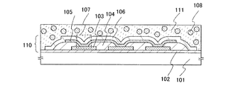
第1の電極層及び第2の電極層からなる一対の電極間に有機化合物を含む層を有する記憶素子と、当該記憶素子を有する素子層と、素子層上に形成される封止層を有し、封止層には吸湿材が含まれていることを特徴とする記憶装置である。 A memory element having a layer containing an organic compound between a pair of electrodes including a first electrode layer and a second electrode layer, an element layer having the memory element, and a sealing layer formed over the element layer In the storage device, the hygroscopic material is included in the sealing layer.
また、第1の電極層及び第2の電極層からなる一対の電極間に有機化合物を含む層を有する記憶素子と、当該記憶素子及び半導体素子を有する素子層と、素子層上に形成される封止層とを有し、封止層には吸湿材が含まれていることを特徴とする半導体装置である。 Further, a memory element having a layer containing an organic compound between a pair of electrodes including the first electrode layer and the second electrode layer, an element layer having the memory element and the semiconductor element, and an element layer are formed. The semiconductor device includes a sealing layer, and the sealing layer includes a hygroscopic material.
吸湿材としては、溶融シリカ、結晶シリカ、アルミナ、窒化珪素、窒化アルミニウム、窒化ホウ素、ゼオライト、アルカリ土類金属の酸化物、金属の硫酸塩、または高吸水性ポリマーの粒子で形成される。吸湿材の粒径は、粒径1μm以上100μm以下、好ましくは5μm以上30μm以下、更に好ましくは5μm以上10μm以下である。 The hygroscopic material is formed of fused silica, crystalline silica, alumina, silicon nitride, aluminum nitride, boron nitride, zeolite, alkaline earth metal oxide, metal sulfate, or highly water-absorbing polymer particles. The particle size of the hygroscopic material is 1 μm or more and 100 μm or less, preferably 5 μm or more and 30 μm or less, and more preferably 5 μm or more and 10 μm or less.
封止層としては、フッ素含有ポリマー―、ポリオレフィン、ポリアクリロニトリル、ポリアミド、ポリエステル、エポキシ樹脂の高分子材料で形成される。 The sealing layer is formed of a polymer material such as a fluorine-containing polymer, polyolefin, polyacrylonitrile, polyamide, polyester, or epoxy resin.
また、半導体素子としては、MOSトランジスタ、薄膜トランジスタ、有機半導体トランジスタ等のトランジスタ、容量素子、抵抗素子等がある。また、素子層には、アンテナを含んでもよい。 Examples of the semiconductor element include a transistor such as a MOS transistor, a thin film transistor, and an organic semiconductor transistor, a capacitor element, a resistance element, and the like. The element layer may include an antenna.
また、本発明の記憶装置及び半導体装置は情報を記憶する機能を有する。また、本発明の記憶装置及び半導体装置は、無線信号により命令やデータの送受信を行うと共に、当該無線信号で送受信した情報や、命令による処理結果を記憶する機能を有する。 In addition, the memory device and the semiconductor device of the present invention have a function of storing information. In addition, the storage device and the semiconductor device of the present invention have functions of transmitting and receiving commands and data by wireless signals and storing information transmitted and received by wireless signals and processing results by the commands.
本発明の記憶装置及び半導体装置は、第1の電極層及び第2の電極層からなる一対の電極間に有機化合物を含む層を有する記憶素子と、記憶素子を有する素子層と、素子層上に形成される封止層を有し、当該封止層には吸湿材が含まれている。封止層に吸湿材が含まれていることにより、記憶装置または半導体装置に曝される雰囲気中の水分が封止層に侵入しても、封止層に含まれる吸湿材で当該水分を吸収することができる。このため、第1の電極層及び第2の電極層からなる一対の電極間に有機化合物を含む層を有する記憶素子が、水分に接触することを低減することが可能である。 A memory device and a semiconductor device of the present invention include a memory element including a layer containing an organic compound between a pair of electrodes including a first electrode layer and a second electrode layer, an element layer including the memory element, and an element layer And a hygroscopic material is contained in the sealing layer. By including a hygroscopic material in the sealing layer, even if moisture in the atmosphere exposed to the memory device or the semiconductor device enters the sealing layer, the moisture is absorbed by the hygroscopic material included in the sealing layer. can do. For this reason, it is possible to reduce a memory element having a layer containing an organic compound between a pair of electrodes including the first electrode layer and the second electrode layer from coming into contact with moisture.
この結果、第1の電極、第2の電極、有機化合物を含む層等が水分や蒸気により劣化することを低減することが可能である。また、記憶素子の記憶保持特性の経年変化を抑制することが可能であり、記憶機能の信頼性の高い記憶装置及び半導体装置を作製することができる。また、素子層及び封止層を可撓性基板上に設けることにより、極めて薄く、フレキシブルで、且つ記憶保持能力の信頼性の高い記憶装置及び半導体装置を作製することができる。 As a result, it is possible to reduce deterioration of the first electrode, the second electrode, the layer containing an organic compound, and the like due to moisture or steam. In addition, it is possible to suppress the secular change in the memory retention characteristics of the memory element, and a memory device and a semiconductor device with high reliability of the memory function can be manufactured. In addition, by providing the element layer and the sealing layer over a flexible substrate, a memory device and a semiconductor device which are extremely thin, flexible, and have high memory retention capability can be manufactured.
本発明の実施の形態について図面を参照して説明する。但し、本発明は以下の説明に限定されず、本発明の趣旨及びその範囲から逸脱することなくその形態及び詳細を様々に変更し得ることは当業者であれば容易に理解される。従って、本発明は、以下に示す実施の形態の記載内容に限定して解釈されるものではない。なお、以下に説明する本発明の構成において、同じものを指す符号は異なる図面間で共通して用いる。 Embodiments of the present invention will be described with reference to the drawings. However, the present invention is not limited to the following description, and it is easily understood by those skilled in the art that modes and details can be variously changed without departing from the spirit and scope of the present invention. Therefore, the present invention should not be construed as being limited to the description of the embodiments below. Note that in the structures of the present invention described below, the same reference numerals are used in common in different drawings.
(実施の形態1)
本実施の形態では、本発明の記憶装置の主要な構成について示す。代表的形態として、記憶素子が設けられたメモリセルを有する記憶装置を図1、2、及び4を用いて説明する。なお、各メモリ素子は、第1の電極層及び第2の電極層からなる一対の電極間に有機化合物を含む層を有しており、メモリセルは記憶装置内でマトリクス状に配列されている。また、記憶素子の構造については、図3を用いて説明する。
(Embodiment 1)
In this embodiment mode, a main structure of a memory device of the present invention is shown. As a typical embodiment, a memory device including a memory cell provided with a memory element will be described with reference to FIGS. Note that each memory element includes a layer containing an organic compound between a pair of electrodes including a first electrode layer and a second electrode layer, and the memory cells are arranged in a matrix in the memory device. . Further, the structure of the memory element will be described with reference to FIG.
図4(A)に示すように、記憶装置127はメモリセルアレイ132及びメモリセルアレイを駆動する駆動回路を有する。メモリセルアレイ132には、メモリセル21がマトリクス状に設けられている。メモリセル21は、記憶素子107を有する(図1参照。)。記憶素子107は、基板101上に、第1の方向に延びた第1の電極層103と、第1の電極層103を覆う有機化合物を含む層105と、第1の方向と交差する第2の方向に延びた第2の電極層106とを有する。また、第2の電極層106を覆うように、保護膜として機能する絶縁層を設けてもよい。
As shown in FIG. 4A, the
図4(A)に示すメモリセルアレイ132の断面構造について、図1及び2を用いて説明する。
A cross-sectional structure of the
図1に示すように、基板101上に下地膜として機能する絶縁層102が形成される。絶縁層102上に第1の電極層103が形成され、第1の電極層103及び下地膜として機能する絶縁層102上に、絶縁層(または隔壁)104が形成される。なお、絶縁層(または隔壁)104は第1の電極層103を露出するように開口部が形成される。絶縁層(または隔壁)104及び第1の電極層上に有機化合物を含む層105が形成される。有機化合物を含む層105、絶縁層(または隔壁)104、及び下地膜として機能する絶縁層102上に第2の電極層106が形成される。
As shown in FIG. 1, an
第1の電極層103、有機化合物を含む層105、及び第2の電極層106により、記憶素子107を構成する。ここでは、下地膜として機能する絶縁層102から第2の電極層106までの積層物を素子層110という。
A
また、素子層110上に吸湿材108を含む封止層111が形成される。
In addition, the
封止層111は、塗布法を用いて組成物を塗布し、加熱または光照射による硬化により形成することが好ましい。封止層111は、後の剥離工程での保護層として設けるため、表面の凹凸の少ない絶縁層であることが好ましい。このような絶縁層は、塗布法により形成することができる。
The
塗布法を用いて形成された封止層111は、フッ素含有ポリマー、ポリオレフィン、ポリアクリロニトリル、ポリアミド、ポリエステル、エポキシ樹脂、あるいはシロキサンポリマーを出発材料として形成された、シリカガラスに代表される無機シロキサンポリマー、又はアルキルシロキサンポリマー、アルキルシルセスキオキサンポリマー、水素化シルセスキオキサンポリマー、水素化アルキルシルセスキオキサンポリマーに代表される、珪素上の水素がメチル基やフェニル基のような有機基によって置換された有機シロキサンポリマーで形成される。
The
フッ素含有ポリマーの代表例としては、ポリテトラフルオロエチレン、ポリクロロトリフルオロエチレン、ポリビニデンフルオライド、エチレン−テトラフルオロエチレン共重合体等がある。 Typical examples of the fluorine-containing polymer include polytetrafluoroethylene, polychlorotrifluoroethylene, polyvinylidene fluoride, and ethylene-tetrafluoroethylene copolymer.
ポリオレフィンの代表例としては、ポリエチレン、ポリプロピレン、ポリブタジエン、ポリイソプレン、ポリスチレン等の重合体およびこれらの共重合体がある。 Typical examples of polyolefin include polymers such as polyethylene, polypropylene, polybutadiene, polyisoprene, polystyrene, and copolymers thereof.
エポキシ樹脂の代表例としては、クレゾールノボラック型エポキシ樹脂、ジシクロペンタジエン型エポキシ樹脂、トリフェニルメタン型エポキシ樹脂、ブロム含有エポキシ樹脂、ナフタレン環を有するエポキシ樹脂等がある。 Typical examples of the epoxy resin include a cresol novolac type epoxy resin, a dicyclopentadiene type epoxy resin, a triphenylmethane type epoxy resin, a bromine-containing epoxy resin, and an epoxy resin having a naphthalene ring.
吸湿材108としては、粒径1μm以上100μm以下、好ましくは5μm以上30μm以下、更に好ましくは5μm以上10μm以下の吸湿性の高い粒子を用いることができる。吸湿性の高い粒子の代表例としては、溶融シリカ、結晶シリカ、アルミナ、窒化珪素、窒化アルミニウム、窒化ホウ素、ゼオライト、アルカリ土類金属の酸化物、金属の硫酸塩、高吸水性ポリマー等の粒子がある。
As the
アルカリ土類金属の酸化物の代表例としては、酸化カルシウム、酸化バリウム、酸化マグネシウム、酸化ストロンチウム等がある。 Typical examples of the alkaline earth metal oxide include calcium oxide, barium oxide, magnesium oxide, and strontium oxide.
金属の硫酸塩の代表例としては、硫酸リチウム、硫酸ナトリウム、硫酸カルシウム、硫酸マグネシウム、硫酸コバルト、硫酸ガリウム、硫酸チタン、硫酸ニッケル等がある。 Typical examples of the metal sulfate include lithium sulfate, sodium sulfate, calcium sulfate, magnesium sulfate, cobalt sulfate, gallium sulfate, titanium sulfate, and nickel sulfate.
高吸水性ポリマーの代表例としては、ポリビニルアルコールやポリビニルピロリドン等のビニルポリマー、或いはポリエーテル、ポリエステル、ポリアミドなどの縮合系ポリマー等がある。なお、高吸水性ポリマーとは、水に溶けることなく、自重の1〜数100倍もの水を吸収し、且つ保持する能力を有するポリマーである。
Typical examples of the superabsorbent polymer include vinyl polymers such as polyvinyl alcohol and polyvinyl pyrrolidone, and condensation polymers such as polyether, polyester and polyamide. The superabsorbent polymer is a polymer that has the ability to absorb and retain
また、吸湿材108の形状は、球状、柱状、または多面体等である。また、水分を吸着する面積を増大させるため、表面が凹凸状であってもよい。また、吸湿材の表面に細孔が形成されていてもよい。
The shape of the
また、封止層111における吸湿材108の割合は限定的ではないが、封止層111を形成する高分子材料、無機シロキサンポリマー、有機シロキサンポリマーに対して1〜20wt%、さらには5〜15wt%含まれることが好ましい。
Further, the ratio of the
封止層111に吸湿材108が含まれることによって、封止層111が吸収した水分を吸湿材108で吸着、吸収することが可能である。このため、記憶装置の外気に含まれる水分が第1の電極層、第2の電極層、有機化合物を含む層等が形成されている素子層110に侵入することを抑制することが可能であり、これらの劣化を防ぐことができる。
By including the
ここでは、封止層111は、吸湿材108として酸化カルシウム粒子が含まれたエポキシ樹脂を塗布法により塗布し、乾燥し焼成して形成する。
Here, the
基板101としては、ガラス基板、石英基板、金属基板やステンレス基板の一表面に絶縁層を形成したもの、本工程の処理温度に耐えうる耐熱性があるプラスチック基板等を用いる。上記に挙げた基板101には、大きさや形状に制約がないため、例えば、基板101として、1辺が1メートル以上であって、矩形状のものを用いれば、生産性を格段に向上させることができる。この利点は、円形のシリコン基板を用いる場合と比較すると、大きな優位点である。
As the
下地膜として機能する絶縁層102は、スパッタリング法やプラズマCVD法、塗布法、印刷法等により、無機化合物を用いて単層又は多層で形成する。無機化合物の代表例としては、酸化珪素、窒化珪素、酸化窒化珪素、窒化酸化珪素等がある。なお、下地膜として機能する絶縁層102に、窒化珪素、窒化酸化珪素、酸化窒化珪素等を用いることにより、後に形成される素子層へ水分や、酸素、二酸化炭素等の気体が外部から侵入することを防止することができる。
The insulating
さらには、下地膜として機能する絶縁層102を積層構造としても良い。例えば、無機化合物を用いて積層してもよく、代表的には、酸化珪素、窒化酸化珪素、及び酸化窒化珪素を積層して形成しても良い。
Further, the insulating
第1の電極層103は、スパッタリング法やプラズマCVD法、塗布法、印刷法、電解メッキ法、無電解メッキ法等を用い、導電性の高い金属、合金、化合物等からなる単層または多層構造を用いて形成することができる。
The
第1の電極層103としては、インジウム錫酸化物(以下、ITOと示す)、または酸化珪素を含有したインジウム錫酸化物、2〜20atomic%の酸化亜鉛(ZnO)を含む酸化インジウム等が挙げられる。また、チタン(Ti)、金(Au)、白金(Pt)、ニッケル(Ni)、タングステン(W)、クロム(Cr)、モリブデン(Mo)、鉄(Fe)、コバルト(Co)、銅(Cu)、パラジウム(Pd)、または金属材料の窒化物(例えば、窒化チタン、窒化タングステン、窒化モリブデン)等を用いることも可能である。
Examples of the
また、第1の電極層103としては、リチウム(Li)やセシウム(Cs)等のアルカリ金属、およびマグネシウム(Mg)、カルシウム(Ca)、ストロンチウム(Sr)等のアルカリ土類金属、アルミニウム(Al)およびこれらのいずれかを含む合金、ユーロピウム(Eu)、イッテルビウム(Yb)等の希土類金属およびこれらのいずれかを含む合金等が挙げられる。
The
また、第1の電極層103として、スズ合金で形成することができる。スズ合金の代表例としては、スズ及び銀の合金、スズ及びビスマスの合金、スズ及びアンチモンの合金、スズ及び銅の合金、スズ及び金の合金、スズ及び亜鉛の合金、スズ及びインジウムの合金等がある。
Further, the
有機化合物を含む層105は、蒸着法、電子ビーム蒸着法、塗布法等を用いて形成することができる。
The
ここでは、50〜200nmのチタン層をスパッタリング法により成膜した後、フォトリソグラフィ法により所望の形状にエッチングして第1の電極層103を形成する。次に、蒸着法によりNPBで形成される有機化合物を含む層を形成する。
Here, after a titanium layer with a thickness of 50 to 200 nm is formed by a sputtering method, the
第2の電極層106は、蒸着法、スパッタリング法、CVD法、印刷法、塗布法等を用いて形成することができる。第2の電極層106は、第1の電極層103と同様の材料を適宜用いて形成することができる。また、第2の電極層106は、スズ合金で形成することができる。スズ合金の代表例としては、スズ及び銀の合金、スズ及びビスマスの合金、スズ及びアンチモンの合金、スズ及び銅の合金、スズ及び金の合金、スズ及び亜鉛の合金、スズ及びインジウムの合金等がある。さらには、銀、ビスマス、アンチモン、銅、金、亜鉛、及びインジウムから選ばれる複種類の元素及びスズとの合金を用いて第2の電極層106を形成してもよい。
The
また、第2の電極層106を積層構造とすることもできる。代表的には、第1の層としてスズ合金層を形成した後、第2の層としてチタン(Ti)、金(Au)、白金(Pt)、ニッケル(Ni)、タングステン(W)、クロム(Cr)、モリブデン(Mo)、鉄(Fe)、コバルト(Co)、銅(Cu)、パラジウム(Pd)、アルミニウム(Al)、マグネシウム(Mg)、または金属材料の窒化物(例えば、窒化チタン、窒化タングステン、窒化モリブデン)等の金属層を形成してもよい。第2の層を形成することで、記憶素子にデータを書き込むときに高電流の通電が生じた場合、第1の層であるスズ合金層が剥れることを防止することができる。
Alternatively, the
ここでは、蒸着法によりスズ及び銀を同時に蒸着して、スズ及び銀合金で第2の電極層106を形成する。
Here, tin and silver are vapor-deposited simultaneously by a vapor deposition method, and the
ここで、記憶素子107のより具体的な構造について図3を用いて以下に示す。
Here, a more specific structure of the
図3(A)に示すように、第1の電極層103及び第2の電極層106に印加された電圧により、結晶状態や導電性、形状が変化するような有機化合物を含む層105を形成することで、記憶素子107が形成される。第1の電極層103及び第2の電極層106に印加された電圧により、有機化合物を含む層105の結晶状態や導電性、形状が変化することで、記憶素子の電気抵抗が変化する。当該変化を用いて、0または1のデータを記録することができる。
As shown in FIG. 3A, a
ここでは、有機化合物を含む層105は有機化合物層300で形成される。なお、有機化合物層300は、単層の有機化合物層または複数の有機化合物層で形成することができる。
Here, the
有機化合物を含む層105の厚さは、第1の電極層103及び第2の電極層106への電圧印加により記憶素子の電気抵抗が変化する厚さが好ましい。有機化合物を含む層105の代表的な膜厚は、1nmから100nm、好ましくは10nmから60nm、更に好ましくは5〜30nmである。
The thickness of the
有機化合物層300は、正孔輸送性を有する有機化合物又は電子輸送性を有する有機化合物を用いて形成することができる。
The
正孔輸送性の有機化合物としては、例えば、フタロシアニン(略称:H2Pc)、銅フタロシアニン(略称:CuPc)、バナジルフタロシアニン(略称:VOPc)の他、4,4’,4’’−トリス(N,N−ジフェニルアミノ)トリフェニルアミン(略称:TDATA)、4,4’,4’’−トリス[N−(3−メチルフェニル)−N−フェニルアミノ]トリフェニルアミン(略称:MTDATA)、1,3,5−トリス[N,N−ジ(m−トリル)アミノ]ベンゼン(略称:m−MTDAB)、N,N’−ジフェニル−N,N’−ビス(3−メチルフェニル)−1,1’−ビフェニル−4,4’−ジアミン(略称:TPD)、4,4’−ビス[N−(1−ナフチル)−N−フェニルアミノ]ビフェニル(略称:NPB)、4,4’−ビス{N−[4−ジ(m−トリル)アミノ]フェニル−N−フェニルアミノ}ビフェニル(略称:DNTPD)、4,4’−ビス[N−(4−ビフェニリル)−N−フェニルアミノ]ビフェニル(略称:BBPB)、4,4’,4’’−トリ(N−カルバゾリル)トリフェニルアミン(略称:TCTA)などが挙げられるが、これらに限定されることはない。ここに述べた物質は、主に10−6cm2/Vs以上の正孔移動度を有する物質である。 Examples of the hole-transporting organic compound include phthalocyanine (abbreviation: H 2 Pc), copper phthalocyanine (abbreviation: CuPc), vanadyl phthalocyanine (abbreviation: VOPc), and 4,4 ′, 4 ″ -tris ( N, N-diphenylamino) triphenylamine (abbreviation: TDATA), 4,4 ′, 4 ″ -tris [N- (3-methylphenyl) -N-phenylamino] triphenylamine (abbreviation: MTDATA), 1,3,5-tris [N, N-di (m-tolyl) amino] benzene (abbreviation: m-MTDAB), N, N′-diphenyl-N, N′-bis (3-methylphenyl) -1 , 1′-biphenyl-4,4′-diamine (abbreviation: TPD), 4,4′-bis [N- (1-naphthyl) -N-phenylamino] biphenyl (abbreviation: NPB), 4,4′- Screw {N- [4- (M-Tolyl) amino] phenyl-N-phenylamino} biphenyl (abbreviation: DNTPD), 4,4′-bis [N- (4-biphenylyl) -N-phenylamino] biphenyl (abbreviation: BBPB), 4, Examples thereof include, but are not limited to, 4 ′, 4 ″ -tri (N-carbazolyl) triphenylamine (abbreviation: TCTA). The substances described here are mainly substances having a hole mobility of 10 −6 cm 2 / Vs or higher.
電子輸送性を有する有機化合物としては、トリス(8−キノリノラト)アルミニウム(略称:Alq3)、トリス(4−メチル−8−キノリノラト)アルミニウム(略称:Almq3)、ビス(10−ヒドロキシベンゾ[h]−キノリナト)ベリリウム(略称:BeBq2)、ビス(2−メチル−8−キノリノラト)−4−フェニルフェノラト−アルミニウム(略称:BAlq)等キノリン骨格またはベンゾキノリン骨格を有する金属錯体を用いることができる。また、この他、ビス[2−(2−ヒドロキシフェニル)ベンゾオキサゾラト]亜鉛(略称:Zn(BOX)2)、ビス[2−(2−ヒドロキシフェニル)ベンゾチアゾラト]亜鉛(略称:Zn(BTZ)2)などのオキサゾール、チアゾール配位子を有する金属錯体などの材料も用いることができる。さらに、金属錯体以外にも、2−(4−ビフェニリル)−5−(4−tert−ブチルフェニル)−1,3,4−オキサジアゾール(略称:PBD)、1,3−ビス[5−(p−tert−ブチルフェニル)−1,3,4−オキサジアゾール−2−イル]ベンゼン(略称:OXD−7)、3−(4−tert−ブチルフェニル)−4−フェニル−5−(4−ビフェニリル)−1,2,4−トリアゾール(略称:TAZ)、3−(4−tert−ブチルフェニル)−4−(4−エチルフェニル)−5−(4−ビフェニリル)−1,2,4−トリアゾール(略称:p−EtTAZ)、バソフェナントロリン(略称:BPhen)、バソキュプロイン(略称:BCP)等を用いることができる。ここに述べた物質は、主に10−6cm2/Vs以上の電子移動度を有する物質である。 As the organic compound having an electron transporting property, tris (8-quinolinolato) aluminum (abbreviation: Alq 3 ), tris (4-methyl-8-quinolinolato) aluminum (abbreviation: Almq 3 ), bis (10-hydroxybenzo [h ] -Quinolinato) beryllium (abbreviation: BeBq 2 ), bis (2-methyl-8-quinolinolato) -4-phenylphenolato-aluminum (abbreviation: BAlq), or the like, a metal complex having a quinoline skeleton or a benzoquinoline skeleton may be used. it can. In addition, bis [2- (2-hydroxyphenyl) benzoxazolate] zinc (abbreviation: Zn (BOX) 2 ), bis [2- (2-hydroxyphenyl) benzothiazolate] zinc (abbreviation: Zn (BTZ) A material such as a metal complex having an oxazole or thiazole ligand such as 2 ) can also be used. In addition to metal complexes, 2- (4-biphenylyl) -5- (4-tert-butylphenyl) -1,3,4-oxadiazole (abbreviation: PBD), 1,3-bis [5- (P-tert-butylphenyl) -1,3,4-oxadiazol-2-yl] benzene (abbreviation: OXD-7), 3- (4-tert-butylphenyl) -4-phenyl-5- ( 4-biphenylyl) -1,2,4-triazole (abbreviation: TAZ), 3- (4-tert-butylphenyl) -4- (4-ethylphenyl) -5- (4-biphenylyl) -1,2, 4-triazole (abbreviation: p-EtTAZ), bathophenanthroline (abbreviation: BPhen), bathocuproin (abbreviation: BCP), and the like can be used. The substances mentioned here are mainly substances having an electron mobility of 10 −6 cm 2 / Vs or higher.
なお、上記範囲外の移動度を有する物質であっても良く、例えば2,3−ビス(4−ジフェニルアミノフェニル)キノキサリン(略称:TPAQn)、9−[4−(N−カルバゾリル)]フェニル−10−フェニルアントラセン(以下、CzPAと記す。)等を用いて形成してもよい。 Note that a substance having mobility outside the above range may be used. For example, 2,3-bis (4-diphenylaminophenyl) quinoxaline (abbreviation: TPAQn), 9- [4- (N-carbazolyl)] phenyl- It may be formed using 10-phenylanthracene (hereinafter referred to as CzPA) or the like.
また、有機化合物層300は上記に示す有機化合物を複数混合して形成してもよい。また、上記に示す有機化合物を積層して形成してもよい。
The
また、有機化合物層300は、正孔輸送性もしくは電子輸送性を有する有機化合物に絶縁物が混合されていても良い。なお、絶縁物は、均一に分散されている必要はない。絶縁物を混合することにより、有機化合物層300のモルフォロジーを向上することができる。よって、部分的な膜の結晶化を抑制することができるため、さらに記憶素子毎の挙動のばらつきを抑制することができる。
In the
また、図3(B)に示すように、有機化合物を含む層105として、有機化合物層300及びバッファ層301で形成してもよい。バッファ層301は、熱的及び化学的に安定な無機化合物または有機化合物で形成する。代表的には、無機絶縁物、無機半導体、または有機絶縁物で形成する。
3B, the
バッファ層301が無機絶縁物または有機絶縁物の場合は、トンネル効果により第1の電極層または第2の電極層から有機化合物層へ、正孔又は電子の電荷を注入する層である。バッファ層301は、所定の電圧において、トンネル効果により有機化合物層300へ電荷を注入することが可能な厚さで形成する。バッファ層301の代表的な厚さは、0.1nm以上4nm以下、好ましくは0.1nm以上2nm以下の絶縁層である。バッファ層301の膜厚は、0.1nm以上4nm以下と極めて薄いため、バッファ層301においてトンネル効果が生じ、有機化合物層300への電荷注入性が高まる。このため、バッファ層301は、厚さが4nmより厚くなると、バッファ層301におけるトンネル効果が生じず、有機化合物層300への電荷注入が困難となり、記憶素子の書き込み時の印加電圧が上昇する。
In the case where the
バッファ層301を形成する無機絶縁物の代表例としては、酸化リチウム、酸化ナトリウム、酸化カリウム、酸化ルビジウム、酸化ベリリウム、酸化マグネシウム、酸化カルシウム、酸化ストロンチウム、酸化バリウム、酸化セシウム、酸化ジルコニウム、酸化ハフニウム、酸化フランシウム、酸化タンタル、酸化テクネチウム、酸化マンガン、酸化鉄、酸化コバルト、酸化パラジウム、酸化銀、アルミナ、酸化ガリウム、酸化ビスマス等に代表される絶縁性を有する酸化物が挙げられる。
Typical examples of the inorganic insulator forming the
また、バッファ層301を形成する無機絶縁物の代表例としては、フッ化リチウム、フッ化ナトリウム、フッ化カリウム、フッ化セシウム、フッ化ベリリウム、フッ化マグネシウム、フッ化カルシウム、フッ化ストロンチウム、フッ化バリウム、フッ化アルミニウム、フッ化銀、フッ化マンガン等に代表される絶縁性を有するフッ化物、塩化リチウム、塩化ナトリウム、塩化カリウム、塩化セシウム、塩化ベリリウム、塩化カルシウム、塩化バリウム、塩化アルミニウム、塩化スズ、塩化銀、塩化亜鉛、塩化チタン、塩化ストロンチウム、塩化鉄、塩化パラジウム、塩化アンチモン、塩化ストロンチウム、塩化タリウム、塩化銅、塩化マンガン、塩化ルテニウム等に代表される絶縁性を有する塩化物、臭化カルシウム、臭化セシウム、臭化銀、臭化バリウム、臭化リチウム等に代表される絶縁性を有する臭化物、ヨウ化ナトリウム、ヨウ化カリウム、ヨウ化バリウム、ヨウ化タリウム、ヨウ化銀、ヨウ化チタン、ヨウ化カルシウム、ヨウ化珪素、ヨウ化セシウム等に代表される絶縁性を有するヨウ化物が挙げられる。
As a typical example of the inorganic insulator forming the
また、バッファ層301を形成する無機絶縁物の代表例としては、炭酸リチウム、炭酸カルシウム、炭酸ナトリウム、炭酸マンガン、炭酸ストロンチウム、炭酸バリウム、炭酸鉄、炭酸コバルト、炭酸ニッケル、炭酸銅、炭酸銀、炭酸亜鉛等に代表される絶縁性を有する炭酸塩、硫化リチウム、硫化カルシウム、硫化ナトリウム、硫化マグネシウム、硫化ストロンチウム、硫化バリウム、硫化チタン、硫化ジルコニウム、硫化マンガン、硫化鉄、硫化コバルト、硫化ニッケル、硫化銅、硫化銀、硫化亜鉛、硫化アルミニウム、硫化インジウム、硫化スズ、硫化アンチモン、硫化ビスマス等に代表される絶縁性を有する硫酸塩、硝酸リチウム、硝酸カリウム、硝酸ナトリウム、硝酸マグネシウム、硝酸カルシウム、硝酸ストロンチウム、硝酸バリウム、硝酸チタン、硝酸ジルコニウム、硝酸マンガン、硝酸鉄、硝酸コバルト、硝酸ニッケル、硝酸銅、硝酸銀、硝酸亜鉛、硝酸アルミニウム、硝酸インジウム、硝酸スズ等に代表される絶縁性を有する硝酸塩、窒化アルミニウム、窒化珪素等に代表される絶縁性を有する窒化物が挙げられる。
As typical examples of the inorganic insulator forming the
なお、バッファ層301を無機絶縁物で形成する場合、バッファ層301の膜厚は、0.1nm以上4nm以下が好ましい。絶縁層の膜厚が4nm以上になると、書き込み時の印加電圧が上昇する。
Note that in the case where the
バッファ層301を形成する有機絶縁物の代表例としては、ポリイミド、アクリル樹脂、ポリアミド、ベンゾシクロブテン樹脂、ポリエステル、ノボラック樹脂、メラミン樹脂、フェノール樹脂、エポキシ樹脂、シリコーン樹脂、フラン樹脂、ジアリルフタレート樹脂等に代表される有機化合物が挙げられる。
Typical examples of the organic insulator forming the
バッファ層301を形成する無機半導体の代表例としては、シリコン、ゲルマニウム、酸化モリブデン、酸化スズ、酸化ビスマス、酸化バナジウム、酸化チタン、酸化鉄、酸化クロム、酸化銅、酸化マンガンシリコン、酸化ニッケル、酸化亜鉛、シリコンゲルマニウム、ヒ化ガリウム、窒化ガリウム、酸化インジウム、リン化インジウム、窒化インジウム、硫化カドミウム、テルル化カドミウム、チタン酸ストロンチウムなどの半導体を用いることができる。なお、バッファ層301は必ずしも一種の半導体から構成される必要はなく、複数の半導体材料が混合されていても良い。
Typical examples of the inorganic semiconductor forming the
なお、バッファ層301を無機半導体で形成する場合、バッファ層301の膜厚は、0.1nm以上であれば特に限定されず、例えば10nm以下の薄い膜厚でも良いし、それ以上であっても良い。
Note that in the case where the
また、バッファ層301は異なる無機絶縁物、有機絶縁物、半導体で形成された層を単層で設けてもよいし、異なる無機絶縁物、有機絶縁物、半導体で形成された層を積層させて複数層としても良い。例えば、無機絶縁物層及び半導体層の積層、無機絶縁物層及び有機絶縁物層の積層、有機絶縁物層及び半導体層の積層等を適宜用いることができる。
The
バッファ層301の形成方法としては、蒸着法、電子ビーム蒸着法、スパッタリング法、CVD法等を用いることができる。また、スピンコート法、ゾル−ゲル法、印刷法または液滴吐出法等を用いることができる。
As a method for forming the
また、図3(C)に示すように、有機化合物を含む層105として、有機化合物層300及び凹凸を有する連続的なバッファ層302を用いて形成してもよい。但し、バッファ層の凸部における厚さは0.1nm以上10nm以下、好ましくは2nm以上8nm以下、凹部における厚さは、0.1nm以上4nm未満、好ましくは0.1nm以上2nm未満であることが好ましい。
As shown in FIG. 3C, the
また、図3(D)に示すように、有機化合物を含む層105として、有機化合物層300及び分散された非連続な絶縁層303を用いて形成してもよい。非連続な絶縁層303は、島状、縞状、網目状等の形状を有してもよい。
Alternatively, as illustrated in FIG. 3D, the
更には、バッファ層301〜303の代わりに、絶縁性粒子を設けてもよい。このときの絶縁性粒子は、粒径は0.1nm以上4nm以下であることが好ましい。 Furthermore, insulating particles may be provided instead of the buffer layers 301 to 303. The insulating particles at this time preferably have a particle size of 0.1 nm to 4 nm.
なお、図3(B)〜(D)では、第1の電極層103及び有機化合物層300の間にバッファ層301〜303を設けたが、第2の電極層106及び有機化合物層300の間にバッファ層301〜303を設けてもよい。
3B to 3D, the buffer layers 301 to 303 are provided between the
さらには、図3(E)に示すように、第1の電極層103及び有機化合物層300の間と、有機化合物層300及び第2の電極層106の間に、上記バッファ層301〜303または絶縁性粒子を設けてもよい。
Further, as shown in FIG. 3E, the buffer layers 301 to 303 or between the
第1の電極層103及び有機化合物層300の間、または有機化合物層300及び第2の電極層106の間に、厚さが4nm以下、好ましくは2nm以下の無機絶縁物または有機絶縁物で形成されるバッファ層を設けることにより、当該絶縁層にトンネル電流が流れるため、記憶素子の書き込み時の印加電圧及び電流値のばらつきを低減することが可能である。また、第1の電極層103及び有機化合物層300の間、または有機化合物層300及び第2の電極層106の間に、厚さが4nm以下、好ましくは2nm以下の無機絶縁物または有機絶縁物で形成されるバッファ層を設けることにより、トンネル効果による電荷注入性が上昇し、有機化合物層300の膜厚を厚くすることが可能であり、初期状態でのショートを防止することが可能である。この結果、記憶装置及び半導体装置の信頼性を向上させることが可能である。
Formed between the
また、上記構成とは異なる構成として、第1の電極層103及び有機化合物を含む層105の間、もしくは第2の電極層106と有機化合物を含む層105の間に、整流作用を有する素子を設けてもよい(図3(F))。整流作用を有する素子とは、代表的には、ショットキーダイオード、PN接合を有するダイオード、PIN接合を有するダイオード、あるいはゲート電極とドレイン電極を接続したトランジスタ等がある。もちろん、他の構成のダイオードでも構わない。ここでは、第1の電極層103と有機化合物を含む層105の間に、半導体層304、305を含むPN接合ダイオード306を設けた場合を示す。半導体層304、305のうち、一方はN型半導体であり、他方はP型半導体である。このように整流作用を有する素子を設けることにより、読み出し特性や書き込み特性を向上させることができる。
Further, as a structure different from the above structure, an element having a rectifying action is provided between the
また、基板上に形成した素子層及び封止層を剥して、図2(A)に示すような、可撓性を有する記憶装置113としてもよい。この場合、下地膜として機能する絶縁層102を、パッシベーション効果の有する層で形成することが好ましい。代表的な絶縁層102としては、窒化珪素層、窒化酸化珪素層を用いて形成することが好ましい。
Alternatively, the element layer and the sealing layer formed over the substrate may be peeled off to form a
基板上に形成した素子層及び封止層を剥すために、基板及び下地膜として機能する絶縁層102の間に剥離層を形成することが好ましい。換言すると、基板から素子層及び封止層を容易に剥すために剥離層を用いることが好ましい。
In order to peel off the element layer and the sealing layer formed over the substrate, a separation layer is preferably formed between the substrate and the insulating
剥離層としては、スパッタリング法やプラズマCVD法、塗布法、印刷法等により、タングステン(W)、モリブデン(Mo)、チタン(Ti)、タンタル(Ta)、ニオブ(Nb)、ニッケル(Ni)、コバルト(Co)、ジルコニウム(Zr)、亜鉛(Zn)、ルテニウム(Ru)、ロジウム(Rh)、パラジウム(Pd)、オスミウム(Os)、イリジウム(Ir)、及び珪素(Si)の中から選択された元素、又は元素を主成分とする合金、又は元素を主成分とする化合物(代表的には、酸化物または窒化物)からなる層を、単層は複数の層を積層させて形成する。珪素を剥離層として用いる場合には、珪素を含む層の結晶構造は、非晶質、微結晶、多結晶のいずれの場合でもよい。 As the release layer, tungsten (W), molybdenum (Mo), titanium (Ti), tantalum (Ta), niobium (Nb), nickel (Ni), sputtering, plasma CVD, coating, printing, etc. Selected from cobalt (Co), zirconium (Zr), zinc (Zn), ruthenium (Ru), rhodium (Rh), palladium (Pd), osmium (Os), iridium (Ir), and silicon (Si) A single layer is formed by stacking a plurality of layers, each of which includes a single element, an alloy containing the element as a main component, or a compound containing the element as a main component (typically an oxide or a nitride). In the case of using silicon as a release layer, the crystal structure of the layer containing silicon may be any of amorphous, microcrystalline, and polycrystalline.
剥離方法の一例としては、剥離層として上記金属のいずれかで形成される金属層及び当該金属酸化物層を形成し、剥離層を有する基板101及び素子層110を物理的手段により剥離する方法がある。物理的手段とは、力学的手段または機械的手段を指し、何らかの力学的エネルギー(機械的エネルギー)を半導体装置へ与える手段を指している。物理的手段は、代表的には機械的な力を加えること(例えば人間の手や把持具による剥離や、ローラを回転させる分離処理)である。
As an example of a peeling method, there is a method in which a metal layer formed of any of the above metals and the metal oxide layer are formed as a peeling layer, and the
また、他の剥離方法の一例としては、基板と素子層との間に、剥離層として水素を含む非晶質珪素層を設け、レーザ光の照射により非晶質珪素層に含まれる水素ガスを放出させて基板を剥離する方法がある。 As another example of the peeling method, an amorphous silicon layer containing hydrogen is provided as a peeling layer between a substrate and an element layer, and hydrogen gas contained in the amorphous silicon layer is irradiated by laser irradiation. There is a method of releasing and releasing the substrate.
また、他の剥離方法の一例としては、基板と素子層との間に金属層及び金属酸化物層を有する剥離層を形成し、当該金属酸化物層を結晶化により脆弱化し、剥離層を液体のエッチャントやNF3、あるいはBrF3、ClF3等のフッ化ハロゲンガスによりエッチングで除去する方法がある。 As another example of the peeling method, a peeling layer having a metal layer and a metal oxide layer is formed between a substrate and an element layer, the metal oxide layer is weakened by crystallization, and the peeling layer is liquidized. there is a method of removing by etching by the etchant or NF 3 or BrF 3, ClF 3 halogen fluoride gas such as,.
また、他の剥離方法の一例としては、素子層110及び封止層111が形成された基板101のみを機械的に削除する、又は基板101をエッチングで除去する方法がある。
As another example of the peeling method, there is a method in which only the
また、他の剥離方法の一例としては、基板101と素子層110との間に剥離層として金属層及び金属酸化物層を設け、当該金属酸化物層を結晶化により脆弱化し、金属層の一部を液体のエッチャントやNF3、あるいはBrF3、ClF3等のフッ化ハロゲンガスによりエッチングで除去した後、上記物理的方法を用いて脆弱化された金属酸化物層において物理的に剥離する方法がある。
As another example of the peeling method, a metal layer and a metal oxide layer are provided as a peeling layer between the
さらには、図2(B)に示すように、下地膜として機能する絶縁層102に可撓性基板120を接着材122を用いて貼りあわせて記憶装置128を形成してもよい。これにより、可撓性基板120上に素子層110及び封止層111が設けられる。このような記憶装置128は、薄型であり、且つ機械的強度の高い記憶装置である。
Further, as illustrated in FIG. 2B, the
可撓性基板120としては、可撓性を有する基板を用いることが好ましく、薄くて軽いものが好ましい。代表的には、PET(ポリエチレンテレフタレート)、PEN(ポリエチレンナフタレート)、PES(ポリエーテルスルホン)、ポリプロピレン、ポリプロピレンサルファイド、ポリカーボネート、ポリエーテルイミド、ポリフェニレンサルファイド、ポリフェニレンオキサイド、ポリサルフォン、ポリフタールアミド等のプラスチック基板、繊維質な材料からなる紙、セラミックシート等を用いることができる。当該基板を用いる場合、封止層111と可撓性基板120との間に接着材122を設けて、封止層111及び可撓性基板120を貼りあわせる。
As the
また、可撓性基板120として、繊維質な材料からなる紙または基材フィルム(ポリエステル、ポリアミド、無機蒸着フィルム等)と、接着性有機樹脂フィルム(アクリル樹脂、エポキシ樹脂等)との積層フィルムなどを用いることもできる。当該基板を用いる場合、可撓性基板120及び絶縁層102を熱圧着し、接着性有機樹脂フィルムを可塑化させた後、硬化させることで、積層フィルムに絶縁層102を固着させることができる。この場合は、絶縁層102及び可撓性基板120の間に接着材122を別途設ける必要は無い。
In addition, as the
素子層110または封止層111の一方の面に可撓性基板を有することで、このような記憶装置128の機械的強度を高めることが可能である。
By having a flexible substrate on one surface of the
また、図2(C)に示すように、封止層111に接着材123を用いて可撓性基板125を貼り付けて、記憶装置126を形成することができる。即ち、可撓性基板120、125によって素子層110及び封止層111が封止されている。
Further, as illustrated in FIG. 2C, the
このような記憶装置126は素子層及び封止層111の周囲が可撓性基板で封止されているため、機械的強度及び外部環境に対する耐性を高めることが可能である。
In such a
次に、上記で示す記憶装置のデータの書き込み動作及び読み出し動作について図4を用いて示す。 Next, a data write operation and a data read operation of the memory device described above will be described with reference to FIGS.
図4(A)に示すように、メモリセル21は、ワード線Wy(1≦y≦n)に接続される第1の電極層と、ビット線Bx(1≦x≦m)に接続される第2の電極層と、有機化合物を含む層とを有する。有機化合物を含む層は、第1の電極層と第2の電極層の間に設けられる。
As shown in FIG. 4A, the
メモリセルにデータの書き込みを行う際の動作について説明する。データの書き込みは、電気的作用によりデータの書き込みを行う場合について説明する。なお、書き込みはメモリセルの電気特性を変化させることで行うが、メモリセルの初期状態(電気的作用を加えていない状態)をデータ「0」、電気特性を変化させた状態を「1」とする。 An operation when data is written to the memory cell will be described. Data writing will be described in the case where data is written by electrical action. Writing is performed by changing the electrical characteristics of the memory cell. The initial state of the memory cell (the state where no electrical action is applied) is data “0”, and the state where the electrical characteristic is changed is “1”. To do.
メモリセル21にデータ「1」を書き込む場合、まず、デコーダ133、134およびセレクタ135によってメモリセル21を選択する。例えば、デコーダ134によって、メモリセル131に接続されるワード線W3に所定の電圧V2が印加される。また、デコーダ133とセレクタ135によって、メモリセル21に接続されるビット線B3を読み出し/書き込み回路136に接続する。そして、読み出し/書き込み回路136からビット線B3へ書き込み電圧V1を出力する。こうして、当該メモリセル21を構成する第1の電極層と第2の電極層の間には電圧Vw=V1−V2を印加する。電位Vwを適切に選ぶことで、当該導電層間に設けられた有機化合物を含む層の特性を物理的もしくは電気的に変化させ、データ「1」の書き込みを行う。具体的には、読み出し動作電圧において、データ「1」の状態の第1の電極層と第2の電極層の間の電気抵抗が、データ「0」の状態と比して、大幅に小さくなるように変化させるとよく、電圧Vwは5〜15V、あるいは−5〜−15Vとすればよい。例えば、(V1、V2)=(0V、5〜15V)、あるいは(3〜5V、−12〜−2V)などとすることができる。
When writing data “1” in the
なお、非選択のワード線および非選択のビット線には、接続されるメモリセルにデータ「1」が書き込まれないよう制御する。例えば、非選択のワード線および非選択のビット線を浮遊状態とすればよい。メモリセル中のメモリ素子には、ダイオード特性など、選択性を確保できる特性を与える必要がある。 Note that data “1” is controlled not to be written in the memory cell connected to the non-selected word line and the non-selected bit line. For example, unselected word lines and unselected bit lines may be set in a floating state. The memory element in the memory cell needs to be given characteristics such as diode characteristics that can ensure selectivity.
一方、メモリセル21にデータ「0」を書き込む場合は、メモリセル21には電気的作用を加えなければよい。回路動作上は、例えば、「1」を書き込む場合と同様に、デコーダ133、134およびセレクタ135によってメモリセル21を選択するが、読み出し/書き込み回路136からビット線B3への出力電位を、選択されたワード線W3の電位あるいは非選択ワード線の電位と同程度とする。すなわち、メモリセル131を構成する第1の電極層と第2の電極層の間に、メモリセル21の電気特性を変化させない程度の電圧(例えば−5〜5V)を印加すればよい。
On the other hand, when data “0” is written in the
次に、メモリセルからデータの読み出しを行う際の動作について説明する(図4(B)、(C)参照)。データの読み出しは、メモリセルの電気特性が、データ「0」を有するメモリセルとデータ「1」を有するメモリセルとで異なることを利用して行う。例えば、データ「0」を有するメモリセルを構成する第1の電極層と第2の電極層の間の実効的な電気抵抗(以下、単にメモリセルの電気抵抗と呼ぶ)が、読み出し電圧においてR0、データ「1」を有するメモリセルの電気抵抗を、読み出し電圧においてR1とし、電気抵抗の差を利用して読み出す方法を説明する。なお、R1<<R0とする。読み出し/書き込み回路は、読み出し部分の構成として、例えば、図4(B)に示す抵抗素子146と差動増幅器147を用いた回路136を考えることができる。抵抗素子146は抵抗値Rrを有し、R1<Rr<R0であるとする。抵抗素子146の代わりにトランジスタ148を用いても良いし、差動増幅器の代わりにクロックドインバータ149を用いることも可能である(図4(C))。クロックドインバータ149には、読み出しを行うときにHi、行わないときにLowとなる信号又は反転信号が入力される。勿論、回路構成は図4(B)及び(C)に限定されない。
Next, an operation for reading data from a memory cell will be described (see FIGS. 4B and 4C). Data reading is performed by utilizing the fact that the electrical characteristics of the memory cell are different between the memory cell having the data “0” and the memory cell having the data “1”. For example, the effective electrical resistance between the first electrode layer and the second electrode layer constituting the memory cell having data “0” (hereinafter simply referred to as the electrical resistance of the memory cell) is R0 at the read voltage. A method of reading data by using the difference in electric resistance when the electric resistance of the memory cell having data “1” is R1 in the read voltage will be described. Note that R1 << R0. As the structure of the reading / writing circuit, for example, a
メモリセル21からデータの読み出しを行う場合、まず、デコーダ133、134およびセレクタ135によってメモリセル21を選択する。具体的には、デコーダ134によって、メモリセル21に接続されるワード線W3に所定の電圧Vyを印加する。また、デコーダ133とセレクタ135によって、メモリセル21に接続されるビット線B3を読み出し/書き込み回路136の端子Pに接続する。その結果、端子Pの電位Vpは、抵抗素子146(抵抗値Rr)とメモリセル21(抵抗値R0もしくはR1)による抵抗分割によって決定される値となる。従って、メモリセル21がデータ「0」を有する場合には、Vp0=Vy+(V0−Vy)×R0/(R0+Rr)となる。また、メモリセル21がデータ「1」を有する場合には、Vp1=Vy+(V0−Vy)×R1/(R1+Rr)となる。その結果、図4(B)では、VrefをVp0とVp1の間となるように選択することで、図4(C)では、クロックドインバータの変化点をVp0とVp1の間となるように選択することで、出力電位Voutとして、データ「0」/「1」に応じて、Lo/Hi(もしくはHi/Lo)が出力され、読み出しを行うことができる。
When reading data from the
例えば、差動増幅器をVdd=3Vで動作させ、Vy=0V、V0=3V、Vref=1.5Vとする。仮に、R0/Rr=Rr/R1=9とすると、メモリセルのデータが「0」の場合、Vp0=2.7VとなりVoutはHighが出力され、メモリセルのデータが「1」の場合、Vp1=0.3VとなりVoutはLowが出力される。こうして、メモリセルの読み出しを行うことができる。 For example, the differential amplifier is operated at Vdd = 3V, and Vy = 0V, V0 = 3V, and Vref = 1.5V. Assuming that R0 / Rr = Rr / R1 = 9, if the memory cell data is “0”, Vp0 = 2.7 V and Vout is High, and if the memory cell data is “1”, Vp1 = 0.3V and Low is output as Vout. Thus, the memory cell can be read.
上記の方法によると、有機化合物を含む層105の電気抵抗は、抵抗値の相違と抵抗分割を利用して、電圧値で読み取っている。勿論、読み出し方法は、この方法に限定されない。例えば、電気抵抗の差を利用する以外に、電流値の差を利用して読み出しても構わない。また、メモリセルの電気特性が、データ「0」と「1」とで、しきい値電圧が異なるダイオード特性を有する場合には、しきい値電圧の差を利用して読み出しても構わない。
According to the above method, the electric resistance of the
以上により、記憶素子の記憶保持特性の経年変化を抑制することが可能であり、記憶機能の信頼性の高い記憶装置を作製することができる。また、素子層及び封止層を可撓性基板上に設けることにより、極めて薄く、フレキシブルで、且つ記憶保持能力の信頼性の高い記憶装置を作製することができる。 Through the above, it is possible to suppress the secular change in the storage retention characteristics of the memory element and to manufacture a memory device with high reliability of the memory function. In addition, by providing the element layer and the sealing layer over a flexible substrate, a memory device that is extremely thin, flexible, and has high memory retention capability can be manufactured.
(実施の形態2)
本実施の形態では、上記実施の形態で示した記憶装置において、メモリセルにスイッチング素子及び記憶素子を有するメモリセルアレイを有する記憶装置の主要な構成について、図5及び図6を用いて説明する。図5は本実施の形態の記憶装置の断面図を示し、図6は本実施の形態の記憶装置の構造を示す。
(Embodiment 2)
In this embodiment, the main structure of the memory device including the memory cell array including the switching element and the memory element in the memory cell in the memory device described in the above embodiment will be described with reference to FIGS. FIG. 5 shows a cross-sectional view of the memory device of this embodiment, and FIG. 6 shows the structure of the memory device of this embodiment.
なお、図5においては、図2(C)に示す形態の変形例であり、可撓性基板で封止されている素子層及び封止層の形態について示す。また図5では、図1、図2(A)、及び図2(B)に示すような記憶装置の素子層の中にスイッチング素子及び記憶素子が形成されている状態が示されている。 Note that FIG. 5 illustrates a modification example of the mode illustrated in FIG. 2C and illustrates a mode of an element layer and a sealing layer that are sealed with a flexible substrate. FIG. 5 shows a state in which switching elements and memory elements are formed in the element layers of the memory device as shown in FIGS. 1, 2A, and 2B.
図6(A)に示すように、本実施の形態の記憶装置221はメモリセルアレイ222及びメモリセルアレイ222を駆動する駆動回路を有する。メモリセルアレイ222は、複数のメモリセル220がマトリクス状に設けられている。また、図6(A)及び図5に示すように、記憶装置221は、下地膜として機能する絶縁層150上に、駆動回路を構成するトランジスタ、(例えばデコーダ224を構成するトランジスタ152、スイッチング素子として機能するトランジスタ151)及び当該トランジスタ151に接続された記憶素子107が形成される。記憶素子107は、絶縁層205上に形成される第1の電極層103、有機化合物を含む層105、及び第2の電極層106を有する。なお、有機化合物を含む層105は、第1の電極層103、及び第1の電極層103の一部を覆う隔壁として機能する絶縁層104上に形成される。また、トランジスタ151として、薄膜トランジスタを用いている。また、第2の電極層106を覆って保護層として機能する絶縁層(図示せず)を有してもよい。
As shown in FIG. 6A, the
また、下地膜として機能する絶縁層150から第2の電極層106の積層体を覆うように、吸湿材108が含まれる封止層111が形成される。ここでは、封止層111に覆われる積層体を素子層201と示す。
In addition, the
また、素子層201及び封止層111は可撓性基板120、125で封止されている。なお、可撓性基板120は接着材122で素子層201及び封止層111に貼り付けられており、可撓性基板125は接着材123で封止層111に貼り付けられている。
Further, the
封止層111に吸湿材108が含まれることによって、封止層111で吸収した水分を吸湿材108で吸着、吸収することが可能である。このため、記憶装置の外気に含まれる水分が第1の電極層、第2の電極層、有機化合物を含む層等が形成されている素子層201に侵入することを抑制することが可能であり、これらの劣化を防ぐことができる。
By including the
トランジスタ151、152は、Siウエハーを用いたMOSトランジスタ、SOI基板を用いたMOSトランジスタ、薄膜トランジスタ、有機半導体トランジスタ等を適宜用いることができる。ここでは、トランジスタ151、152として薄膜トランジスタを用いて示す。なお、ここでは、薄膜トランジスタとしてトップゲート型の薄膜トランジスタを示しているがこれに限定される物ではない。ボトムゲート型の薄膜トランジスタを適用することが可能である。
As the
記憶素子107は、絶縁層205上に形成される。このように、絶縁層205を設けることによって第1の電極層103を自由にレイアウトすることができる。つまり、トランジスタ151の上方に記憶素子107を形成することが可能となる。その結果、記憶装置をより高集積化することが可能となる。
The
絶縁層205は、上記実施の形態で示した絶縁層104と同様の材料および形成方法を適宜用いて形成することができる。
The insulating
素子層201及び封止層111に貼り付ける可撓性を有する基板としては、実施の形態1の可撓性基板120で示した可撓性基板、熱可塑性樹脂を有するフィルム、繊維質な材料からなる紙、セラミックシート等を用いることで、記憶装置の小型、薄型、軽量化を図ることが可能である。
As the flexible substrate to be attached to the
次に、本実施の形態で示す記憶装置のデータの書き込み動作及び読み出し動作について図6を用いて示す。 Next, data writing and reading operations of the memory device described in this embodiment are described with reference to FIGS.
メモリセル220は、ワード線Wy(1≦y≦n)に接続する第1の電極層と、ビット線Bx(1≦x≦m)に接続する第2の電極層と、トランジスタ151と、記憶素子107とを有する。記憶素子107は、一対の導電層の間に、有機化合物を含む層が挟まれた構造を有する。トランジスタ151のゲート電極はワード線と接続され、ソース電極もしくはドレイン電極のいずれか一方はビット線と接続され、残る一方は記憶素子107が有する第1の電極層と接続される。記憶素子の残る第2の電極層は接続端子と接続される。また、接続端子は共通電極(電位Vcom)と接続される。
The
次に、メモリセルアレイ222にデータの書き込みを行うときの動作について説明する。
Next, an operation when data is written to the
ここでは、3行3列目のメモリセル220に電気的作用によりデータを書き込む場合について説明する。なお、書き込みはメモリセルの電気特性を変化させることで行うが、メモリセルの初期状態(電気的作用を加えていない状態)をデータ「0」、電気特性を変化させた状態を「1」とする。
Here, a case where data is written to the
メモリセル220にデータ「1」を書き込む場合、まず、デコーダ223、224およびセレクタ225によってメモリセル220を選択する。具体的には、デコーダ224によって、メモリセル220に接続されるワード線W3に所定の電圧V22を印加する。また、デコーダ223とセレクタ225によって、メモリセル220に接続されるビット線B3を読み出し/書き込み回路226に接続する。そして、読み出し/書き込み回路226からビット線B3へ書き込み電圧V21を出力する。
When data “1” is written to the
こうして、メモリセルを構成するトランジスタ151をオン状態とし、記憶素子107に、ビット線を電気的に接続し、おおむねVw=Vcom−V21の電圧を印加する。なお、記憶素子107の第2の電極層は電位Vcomの共通電極に接続されている。電位Vwを適切に選ぶことで、当該導電層間に設けられた有機化合物を含む層105の特性を物理的もしくは電気的に変化させ、データ「1」の書き込みを行う。具体的には、読み出し動作電圧において、データ「1」の状態の第1の電極層と第2の電極層の間の電気抵抗が、データ「0」の状態と比して、大幅に小さくなるように変化させるとよく、従って、単に短絡(ショート)させてもよい。なお、電位は、(V21、V22、Vcom)=(5〜15V、5〜15V、0V)、あるいは(−12〜0V、−12〜0V、3〜5V)の範囲から適宜選べば良い。電圧Vwは5〜15V、あるいは−5〜−15Vとすればよい。
Thus, the
なお、非選択のワード線および非選択のビット線には、接続されるメモリセルにデータ「1」が書き込まれないよう制御する。具体的には、非選択のワード線には接続されるメモリセルのトランジスタをオフ状態とする電位(例えば0V)を印加し、非選択のビット線は浮遊状態とするか、Vcomと同程度の電位を印加するとよい。 Note that data “1” is controlled not to be written in the memory cell connected to the non-selected word line and the non-selected bit line. Specifically, a potential (for example, 0 V) for turning off the transistor of the memory cell to be connected is applied to the non-selected word line, and the non-selected bit line is in a floating state or approximately equal to Vcom. A potential may be applied.
一方、メモリセル220にデータ「0」を書き込む場合は、メモリセル220には電気的作用を加えなければよい。回路動作上は、例えば、「1」を書き込む場合と同様に、デコーダ223、224およびセレクタ225によってメモリセル220を選択するが、読み出し/書き込み回路226からビット線B3への出力電位をVcomと同程度とするか、ビット線B3を浮遊状態とする。その結果、記憶素子107には、小さい電圧(例えば−5〜5V)が印加されるか、電圧が印加されないため、電気特性が変化せず、データ「0」書き込みが実現される。
On the other hand, when data “0” is written in the
次に、電気的作用により、データの読み出しを行う際の動作について説明する。データの読み出しは、電気特性が、データ「0」を有する記憶素子とデータ「1」を有する記憶素子とで異なることを利用して行う。例えば、データ「0」を有するメモリセルを構成する記憶素子の電気抵抗が読み出し電圧においてR0、データ「1」を有するメモリセルを構成する記憶素子の電気抵抗が読み出し電圧においてR1とし、電気抵抗の差を利用して読み出す方法を説明する。なお、R1<<R0とする。読み出し/書き込み回路は、読み出し部分の構成として、例えば、図6(B)に示す抵抗素子246と差動増幅器247を用いた回路226を考えることができる。抵抗素子246は抵抗値Rrを有し、R1<Rr<R0であるとする。抵抗素子246の代わりに、トランジスタ250を用いても良いし、差動増幅器の代わりにクロックドインバータ251を用いることも可能である(図6(C))。勿論、回路構成は図6(B)及び(C)に限定されない。
Next, an operation when data is read by electrical action will be described. Data is read using the fact that the electrical characteristics of the memory element having data “0” are different from those of the memory element having data “1”. For example, the electrical resistance of the memory element constituting the memory cell having data “0” is R0 at the read voltage, and the electrical resistance of the memory element constituting the memory cell having data “1” is R1 at the read voltage. A method of reading using the difference will be described. Note that R1 << R0. As the structure of the reading / writing circuit, for example, a
3列3行目メモリセル220からデータの読み出しを行う場合、まず、デコーダ223、224およびセレクタ225によってメモリセル220を選択する。具体的には、デコーダ224によって、メモリセル220に接続されるワード線W3に所定の電圧V24を印加し、トランジスタ151をオン状態にする。また、デコーダ223とセレクタ225によって、メモリセル220に接続されるビット線B3を読み出し/書き込み回路226の端子Pに接続する。その結果、端子Pの電位Vpは、VcomとV0が抵抗素子246(抵抗値Rr)と記憶素子107(抵抗値R0もしくはR1)による抵抗分割によって決定される値となる。従って、メモリセル220がデータ「0」を有する場合には、Vp0=Vcom+(V0−Vcom)×R0/(R0+Rr)となる。また、メモリセル220がデータ「1」を有する場合には、Vp1=Vcom+(V0−Vcom)×R1/(R1+Rr)となる。その結果、図6(B)では、VrefをVp0とVp1の間となるように選択することで、図6(C)では、クロックドインバータの変化点をVp0とVp1の間となるように選択することで、出力電位Voutが、データ「0」/「1」に応じて、Lo/Hi(もしくはHi/Lo)が出力され、読み出しを行うことができる。
When reading data from the
例えば、差動増幅器をVdd=3Vで動作させ、Vcom=0V、V0=3V、Vref=1.5Vとする。仮に、R0/Rr=Rr/R1=9とし、トランジスタ151のオン抵抗を無視できるとすると、メモリセルのデータが「0」の場合、Vp0=2.7VとなりVoutはHighが出力され、メモリセルのデータが「1」の場合、Vp1=0.3VとなりVoutはLowが出力される。こうして、メモリセルの読み出しを行うことができる。
For example, the differential amplifier is operated at Vdd = 3V, and Vcom = 0V, V0 = 3V, and Vref = 1.5V. Assuming that R0 / Rr = Rr / R1 = 9 and the on-resistance of the
上記の方法によると、記憶素子107の抵抗値の相違と抵抗分割を利用して、電圧値で読み取っている。勿論、読み出し方法は、この方法に限定されない。例えば、電気抵抗の差を利用する以外に、電流値の差を利用して読み出しても構わない。また、メモリセルの電気特性が、データ「0」と「1」とで、しきい値電圧が異なるダイオード特性を有する場合には、しきい値電圧の差を利用して読み出しても構わない。
According to the above method, the voltage value is read by utilizing the difference in resistance value of the
以上により、記憶素子の記憶保持特性の経年変化を抑制することが可能であり、記憶保持機能の信頼性の高い記憶装置を作製することができる。また、素子層及び封止層を可撓性基板上に設けることにより、極めて薄く、フレキシブルで、且つ記憶保持能力の信頼性の高い記憶装置を作製することができる。 Through the above, it is possible to suppress the secular change of the memory retention characteristics of the memory element, and a memory device with high reliability of the memory retention function can be manufactured. In addition, by providing the element layer and the sealing layer over a flexible substrate, a memory device that is extremely thin, flexible, and has high memory retention capability can be manufactured.
(実施の形態3)
本実施の形態では、上記実施の形態で示した剥離方法を用いて形成した半導体装置の一形態について以下に説明する。代表的には、無線信号により命令やデータの送受信を行うことのできる半導体装置の主要な構成について、図7及び図8を用いて説明する。図7は本実施の形態の半導体装置の断面図を示し、図8は本実施の形態の半導体装置の構造を示す。なお、本実施の形態の半導体装置は上記実施の形態で示すメモリセルアレイからなるメモリ部を有する。
(Embodiment 3)
In this embodiment, one embodiment of a semiconductor device formed using the peeling method described in the above embodiment will be described below. Typically, a main structure of a semiconductor device capable of transmitting and receiving commands and data by wireless signals will be described with reference to FIGS. FIG. 7 shows a cross-sectional view of the semiconductor device of this embodiment, and FIG. 8 shows the structure of the semiconductor device of this embodiment. Note that the semiconductor device of this embodiment includes a memory portion including the memory cell array described in the above embodiment.
図8は、無線信号により命令やデータの送受信を行うことのできる半導体装置の一構成例を示すブロック図である。このような半導体装置は、アンテナ312、高周波回路部313、電源回路部315、ロジック回路部317を要素として含んでいる。アンテナ312は、リーダライタとも呼ばれる通信装置と信号の送受信を行う。信号を送る搬送波の周波帯は、長波帯の30〜135kHz、短波帯の6.78MHz、13.56MHz、27.125MHz、40.68MHz、5.0MHz、マイクロ波帯の2.45GHz、5.8GHz、24.125GHz等が適用される。アンテナ312は通信周波数帯に応じてコイル型やモノポール若しくはダイポール型の形態となる。
FIG. 8 is a block diagram illustrating a configuration example of a semiconductor device capable of transmitting and receiving commands and data using wireless signals. Such a semiconductor device includes an
アンテナ312が受信した搬送波は、検波容量部314を介して電源回路部315と、ロジック回路部317に分流する。電源回路部315では整流回路部320によって半波整流され、それが保持容量部322に充電される。定電圧回路部324は受信した搬送波の電力によってある一定以上の電力が供給されても、一定電圧を出力してこの半導体装置にあるロジック回路部317等の動作に必要な電力を供給する。
The carrier wave received by the
高周波回路部313における復調回路部318は、搬送波を復調してロジック回路部317の動作に必要なクロック信号を生成し、さらにそれを補正する機能を有するPLL回路部328と、コード認識及び判定回路部326に信号を出力する。例えば、復調回路部318は、振幅変調(ASK)の受信信号から、振幅の変動を”0”又は”1”の受信データとして検出する。復調回路部318は、例えばローパスフィルターを含んで構成されている。また、変調回路部316は送信データを振幅変調(ASK)の送信信号として送信する。
The
コード認識及び判定回路部326は、命令コードを認識し判定する。各コード認識及び判定回路部326が認識及び判定する命令コードは、フレーム終了信号(EOF、end of frame)、フレーム開始信号(SOF、start of frame)、フラグ、コマンドコード、マスク長(mask length)、マスク値(mask value)等である。また、各コード認識及び判定回路部326は、送信エラーを識別する巡回冗長検査(CRC、cyclic redundancy check)機能も含む。コード認識及び判定回路部326からの結果は、メモリコントローラ部330に出力される。メモリコントローラ部330は、判定結果に基づいて、メモリ部332の読み出しを制御する。メモリ部332から読み出されたデータは、符号化回路部334にて符号化され、変調回路部316によって変調を行い、応答信号が生成する。
The code recognition and
メモリ部332の構成としては、実施の形態1で示すような記憶素子を有するメモリセルや、実施の形態2で示すようなスイッチング素子に接続される記憶素子を有するメモリセルを適宜用いることができる。また、上記実施の形態で示すようなメモリセルの他に固定データのみを記憶するマスクROM(Read Only Memory)、SRAM(Static Random Access Memory)などの任意読み出し書き込み可能メモリ、電荷蓄積浮遊電極を有する不揮発性メモリなどを適用することができる。
As a structure of the
このように、図8で示す半導体装置は、リーダライタとも呼ばれる通信装置からの命令を受信して、メモリ部332にデータを書き込み、若しくはメモリ部332からデータを読み出す機能を有している。
As described above, the semiconductor device illustrated in FIG. 8 has a function of receiving a command from a communication device also called a reader / writer and writing data in the
次に、本実施の形態の半導体装置の断面構造について、図7を用いて説明する。 Next, a cross-sectional structure of the semiconductor device of this embodiment is described with reference to FIGS.
なお、図7においては、図2(C)に示す形態の変形例であり、可撓性基板で封止されている素子層及び封止層の形態について示す。しかし、この実施の形態では、図1、図2(A)、及び図2(B)に示すような記憶装置の素子層に以下の実施の形態に示す記憶装置、アンテナ、半導体素子等が形成される。 Note that FIG. 7 illustrates a modification example of the mode illustrated in FIG. 2C and illustrates a mode of an element layer and a sealing layer that are sealed with a flexible substrate. However, in this embodiment, the memory device, the antenna, the semiconductor element, and the like described in the following embodiments are formed in the element layer of the memory device as illustrated in FIGS. 1, 2A, and 2B. Is done.
ここで、半導体装置の一部として、メモリコントローラ部330、メモリ部332、アンテナ312、及び検波容量部314の断面図を示す(図7参照)。代表的には、下地膜として機能する絶縁層321上に、メモリコントローラ部330を構成するトランジスタ152、メモリ部332を構成するトランジスタ151及び当該トランジスタ151に接続された記憶素子107、検波容量部314の容量素子331及び薄膜トランジスタ333、アンテナ312を示す。なお、ここでは図示しないが、アンテナ312及び薄膜トランジスタ333は電気的に接続している。
Here, as a part of the semiconductor device, a cross-sectional view of the
記憶素子107は、絶縁層205上に形成される第1の電極層103、有機化合物を含む層105、及び第2の電極層106を有する。第2の電極層106は、スズ合金層で形成される。なお、有機化合物を含む層105は、第1の電極層103、及び第1の電極層103の一部を覆う隔壁として機能する絶縁層104上に形成される。また、スイッチング素子として機能するトランジスタ151は、薄膜トランジスタを用いて形成する。また、第2の電極層106を及びアンテナ312を覆って保護層として機能する絶縁層を有してもよい。なお、下地膜として機能する絶縁層150からアンテナ312までの積層体を素子層341と示す。
The
また、素子層341を覆うように吸湿材108が含まれる封止層111が形成される。
Further, the
封止層111に吸湿材108が含まれることによって、封止層111で吸収した水分を吸湿材108で吸着、吸収することが可能である。このため、半導体装置の外気に含まれる水分が第1の電極層、第2の電極層、有機化合物を含む層等が形成されている素子層110に侵入することを抑制することが可能であり、これらの劣化を防ぐことができる。
By including the
また、素子層341及び封止層111が可撓性基板120、125で封止されている。なお、可撓性基板120は接着材122で素子層341及び封止層111に貼り付けられており、可撓性基板125は接着材123で封止層111に貼り付けられている。
In addition, the
本実施の形態により、記憶素子の記憶保持特性の経年変化を抑制することが可能であり、無線で情報を送受信することが可能で、記憶機能の信頼性の高い半導体装置を作製することができる。また、素子層及び封止層を可撓性基板上に設けることにより、極めて薄く、フレキシブルで、無線で情報を送受信することが可能で、且つ記憶保持能力の信頼性の高い半導体装置を作製することができる。 According to this embodiment, it is possible to suppress a secular change in memory retention characteristics of a memory element, transmit / receive information wirelessly, and a semiconductor device with high reliability of a memory function can be manufactured. . Further, by providing the element layer and the sealing layer over a flexible substrate, a semiconductor device which is extremely thin, flexible, can transmit and receive information wirelessly, and has high memory retention capability is manufactured. be able to.
本実施例では、無線信号により命令やデータの送受信を行うことのできる半導体装置において、スイッチング素子に接続される記憶素子がマトリクス状に配置されたメモリセルアレイを有する半導体装置の作製方法について、図9〜図15を用いて以下に説明する。 In this embodiment, a method for manufacturing a semiconductor device having a memory cell array in which memory elements connected to switching elements are arranged in a matrix in a semiconductor device capable of transmitting and receiving commands and data by wireless signals is described with reference to FIGS. It demonstrates below using FIG.
基板501上に剥離層502を形成する。基板501としてはガラス基板を用いる。また、剥離層502としては、金属層及び金属酸化物層の積層構造とする。金属層としては、スパッタリング法により得られる30nm〜200nmのタングステン層、窒化タングステン層、またはモリブデン層を用いる。
A
次に、金属酸化物層としては、金属層の表面を酸化させて金属酸化物層を形成する。金属酸化物層の形成方法は、酸素を含有する純水やオゾン水を用いて表面を酸化して形成してもよいし、酸素プラズマで酸化して形成してもよい。また、酸素を含む雰囲気で加熱を行って金属酸化物層を形成してもよい。また、後の絶縁層の形成工程で形成してもよい。この場合、絶縁層として酸化珪素層や酸化窒化珪素層をプラズマCVD法で形成する際に、剥離層502表面が酸化されて金属酸化物層が形成される。
Next, as the metal oxide layer, the surface of the metal layer is oxidized to form a metal oxide layer. The metal oxide layer may be formed by oxidizing the surface using pure water containing oxygen or ozone water, or by oxidizing with oxygen plasma. Alternatively, the metal oxide layer may be formed by heating in an atmosphere containing oxygen. Moreover, you may form in the formation process of a later insulating layer. In this case, when the silicon oxide layer or the silicon oxynitride layer is formed as the insulating layer by a plasma CVD method, the surface of the
次に、金属酸化物層上に第1絶縁層503を形成する。第1絶縁層503としては、酸化珪素層、窒化珪素層または酸化窒化珪素層等の絶縁層を用いる。代表的な一例は第1絶縁層503として2層構造から成り、PCVD法によりSiH4、NH3、及びN2Oを反応ガスとして成膜される窒化酸化珪素層を50〜100nm、SiH4、及びN2Oを反応ガスとして成膜される酸化窒化珪素層を100〜150nmの厚さに積層形成する構造が採用される。また、第1絶縁層503の一層として膜厚10nm以下の窒化珪素層、或いは酸化窒化珪素層を用いることが好ましい。また、窒化酸化珪素層と、酸化窒化珪素層と、窒化珪素層とを順次積層した3層構造を用いてもよい。ここでは下地絶縁膜として第1絶縁層503を形成した例を示したが、特に必要でなければ設ける必要はない。
Next, the first insulating
次に、第1絶縁層503上に半導体層を形成する。半導体層は、非晶質構造を有する半導体層をスパッタリング法、LPCVD法、またはプラズマCVD法等により成膜する。次に、結晶化処理(レーザ結晶化法、熱結晶化法、またはニッケルなどの触媒を用いた熱結晶化法等)を行って得られた結晶質半導体層上に第1のフォトマスクを用いてレジストマスクを形成した後、所望の形状にエッチングして、半導体層を形成する。なお、プラズマCVD法を用いれば、第1絶縁層と、非晶質構造を有する半導体層とを大気に触れることなく連続的に積層することができる。この半導体層の厚さは25〜80nm(好ましくは30〜70nm)の厚さで形成する。結晶質半導体層の材料に限定はないが、好ましくはシリコンまたはシリコンゲルマニウム合金などで形成すると良い。
Next, a semiconductor layer is formed over the first insulating
また、非晶質構造を有する半導体層を結晶化するために連続発振のレーザを用いてもよく、非晶質半導体層の結晶化に際し、大粒径に結晶を得るためには、連続発振が可能な固体レーザを用い、基本波の第2高調波〜第4高調波を適用するのが好ましい。代表的には、Nd:YVO4レーザー(基本波1064nm)の第2高調波(532nm)や第3高調波(355nm)を適用すればよい。連続発振のレーザを用いる場合には、出力10Wの連続発振のYVO4レーザから射出されたレーザ光を非線形光学素子により高調波に変換する。また、共振器の中にYVO4結晶と非線形光学素子を入れて、高調波を射出する方法もある。そして、好ましくは光学系により照射面にて矩形状または楕円形状のレーザ光に成形して、被処理体に照射する。このときのエネルギー密度は0.01〜100MW/cm2程度(好ましくは0.1〜10MW/cm2)が必要である。そして、10〜2000cm/s程度の速度でレーザ光に対して相対的に半導体層を移動させながら照射すればよい。 In addition, a continuous wave laser may be used to crystallize a semiconductor layer having an amorphous structure, and in order to obtain a crystal with a large grain size when crystallizing an amorphous semiconductor layer, continuous oscillation is required. It is preferable to apply the second to fourth harmonics of the fundamental wave using a possible solid-state laser. Typically, a second harmonic (532 nm) or a third harmonic (355 nm) of an Nd: YVO 4 laser (fundamental wave 1064 nm) may be applied. In the case of using a continuous wave laser, laser light emitted from a continuous wave YVO 4 laser having an output of 10 W is converted into a harmonic by a non-linear optical element. There is also a method of emitting harmonics by putting a YVO 4 crystal and a nonlinear optical element in a resonator. Then, it is preferably formed into a rectangular or elliptical laser beam on the irradiation surface by an optical system, and irradiated to the object to be processed. At this time, the energy density of approximately 0.01 to 100 MW / cm 2 (preferably 0.1 to 10 MW / cm 2) is required. Then, irradiation may be performed while moving the semiconductor layer relative to the laser light at a speed of about 10 to 2000 cm / s.
また、非晶質構造を有する半導体層の結晶化処理としてSLS方式(Sequential Lateral Solidification method)を用いてもよい。SLS法は、パルス発振のエキシマレーザー光を、スリット状のマスクを介して、試料に照射するものである。1ショット毎に、試料とレーザ光の相対位置をスーパーラテラル成長による結晶長さ程度ずらして結晶化を行うことで、人工的に制御したスーパーラテラル成長による結晶を連続的に形成させる方法である。 Further, an SLS method (Sequential Lateral Solidification method) may be used as a crystallization process for a semiconductor layer having an amorphous structure. In the SLS method, a sample is irradiated with pulsed excimer laser light through a slit-shaped mask. This is a method for continuously forming crystals by artificially controlled superlateral growth by performing crystallization by shifting the relative position of the sample and laser light for each shot by the crystal length by superlateral growth.
次に、必要があれば薄膜トランジスタのしきい値を制御するために、微量な不純物元素(ボロンまたはリン)のドーピングを半導体層に対して行う。ここでは、ジボラン(B2H6)を質量分離しないでプラズマ励起したイオンドープ法を用いる。 Next, if necessary, a small amount of impurity element (boron or phosphorus) is doped into the semiconductor layer in order to control the threshold value of the thin film transistor. Here, an ion doping method in which diborane (B 2 H 6 ) is plasma-excited without mass separation is used.
次に、後に容量素子の容量電極となる半導体層に第2フォトマスクを用いてレジストマスクを形成し、不純物元素を導入することにより低濃度不純物領域を形成する。不純物元素としては、n型を付与する不純物元素又はp型を付与する不純物元素を用いることができる。n型を示す不純物元素としては、リン(P)やヒ素(As)等を用いることができる。ここでは、半導体層にリン(P)を1×10¹⁵〜1×10¹⁹/cm3の濃度で含まれるように導入することによりn型を示す不純物領域を形成する。 Next, a resist mask is formed using a second photomask on a semiconductor layer which will later become a capacitor electrode of the capacitor, and an impurity element is introduced to form a low-concentration impurity region. As the impurity element, an impurity element imparting n-type conductivity or an impurity element imparting p-type conductivity can be used. As the impurity element exhibiting n-type, phosphorus (P), arsenic (As), or the like can be used. Here, phosphorus (P) is introduced into the semiconductor layer so as to be contained at a concentration of 1 × 10 15 to 1 × 10 19 / cm 3 , thereby forming an n-type impurity region.
次に、フッ酸を含むエッチャントで半導体層表面の酸化層を除去すると同時に半導体層の表面を洗浄する。 Next, the oxide layer on the surface of the semiconductor layer is removed with an etchant containing hydrofluoric acid, and at the same time, the surface of the semiconductor layer is washed.
次に、半導体層を覆う第2絶縁層を形成する。第2絶縁層はプラズマCVD法またはスパッタリング法を用い、厚さを1〜200nmとする。好ましくは10nm〜50nmと薄くしてシリコンを含む絶縁層の単層または積層構造で形成した後にマイクロ波によるプラズマを用いた表面窒化処理を行う。第2絶縁層は、後に形成される薄膜トランジスタのゲート絶縁層として機能する。 Next, a second insulating layer covering the semiconductor layer is formed. The second insulating layer uses a plasma CVD method or a sputtering method and has a thickness of 1 to 200 nm. Preferably, the insulating layer containing silicon is formed as a single layer or a laminated structure with a thickness of 10 nm to 50 nm, and then surface nitriding treatment using plasma by microwaves is performed. The second insulating layer functions as a gate insulating layer of a thin film transistor to be formed later.
次に、第2絶縁層上にゲート電極504〜507、容量電極508を形成する。スパッタリング法によって膜厚100nm〜500nmで導電層を形成し、この上に第3のフォトマスクを用いてレジストマスクを形成する。そして導電層を所望の形状にエッチングして、ゲート電極504〜507、及び容量電極508を形成する。
Next,
ゲート電極504〜507及び容量電極508の材料としては、シリコンとシリサイド反応する材料であればよく、Ti、W、Ni、Cr、Mo、Ta、Co、Zr、V、Pd、Hf、Pt、Feから選ばれた元素、または前記元素を主成分とする合金若しくは化合物の単層、またはこれらの積層で形成してもよい。ただし、薄膜トランジスタのゲート電極としては高融点金属が好ましく、WまたはMoを用いる。ゲート電極504〜507及び容量電極508を積層とする場合には、上層となる材料層が上述した材料であれば、下層となる材料層は、リン等の不純物元素をドーピングした多結晶シリコン層としてもよい。また、上層に上記材料を用い、下層に上記材料の窒化物で形成してもよい。このとき下層を金属窒化物とすることで、上層の金属が、ゲート絶縁層やその下層の半導体層に拡散することを防ぐことができる。
The material of the
次に、pチャネル型薄膜トランジスタとする領域の半導体層を覆うように第4のフォトマスクを用いてレジストマスクを形成し、nチャネル型薄膜トランジスタとする領域の半導体層にゲート電極505〜507をマスクとして不純物元素を導入することにより低濃度不純物領域を形成する。ここでは、nチャネル型薄膜トランジスタとする領域の半導体層にリン(P)を1×10¹⁵〜1×10¹⁹/cm3の濃度で含まれるように導入することによりn型を示す不純物領域を形成する。
Next, a resist mask is formed using a fourth photomask so as to cover the semiconductor layer in the region to be the p-channel thin film transistor, and the
次に、レジストマスクを除去して、nチャネル型薄膜トランジスタとする半導体層を覆うように第5のフォトマスクを用いてレジストマスクを形成し、pチャネル型薄膜トランジスタとする領域の半導体層にゲート電極504をマスクとして不純物元素を導入することによりp型を示す不純物領域を形成する。p型を示す不純物元素としては、ボロン(B)やアルミニウム(Al)やガリウム(Ga)等を用いることができる。ここでは、pチャネル型薄膜トランジスタとする領域の半導体層にボロン(B)を1×10¹⁹〜1×10²⁰/cm3の濃度で含まれるように導入することによって、p型を示す不純物領域を形成することができる。その結果、pチャネル型薄膜トランジスタとする領域の半導体層に、ソース領域又はドレイン領域514、515、及びチャネル形成領域516が形成される。
Next, the resist mask is removed, a resist mask is formed using a fifth photomask so as to cover the semiconductor layer to be the n-channel thin film transistor, and the
次に、ゲート電極504〜507及び容量電極508の両側面にサイドウォール510を形成する。サイドウォール510は、まず、第2絶縁層、ゲート電極504〜507、及び容量電極508を覆うように、珪素の酸化物又は珪素の窒化物の無機材料を含む層や、有機樹脂等の有機材料を含む層を単層又は積層して第3絶縁層を形成する。第3の絶縁層はプラズマCVD法やスパッタリング法等を適用して形成することができる。次に、第3絶縁層を、垂直方向を主体とした異方性エッチングにより選択的にエッチングすることによって、ゲート電極504〜507、容量電極508の側面に接する絶縁層(サイドウォール510)を形成する。なお、サイドウォール510の形成と同時に、第2絶縁層の一部をエッチングして除去する。第2絶縁層の一部が除去されることによって、残存するゲート絶縁層512は、ゲート電極504〜507、容量電極508、及びサイドウォール510の下方に形成される。
Next, sidewalls 510 are formed on both side surfaces of the
次に、pチャネル型薄膜トランジスタとする半導体層を覆うように第6のフォトマスクを用いてレジストマスクを形成し、nチャネル型薄膜トランジスタとする領域の半導体層にゲート電極504〜507、容量電極508、及びサイドウォール510をマスクとして不純物元素を導入することにより高濃度不純物領域を形成する。不純物元素の導入後にレジストマスクは除去する。ここでは、nチャネル型薄膜トランジスタとする領域の半導体層にリン(P)を1×10¹⁹〜1×10²⁰/cm3の濃度で含まれるように導入することによって、n型を示す高濃度不純物領域を形成することができる。その結果、nチャネル型薄膜トランジスタとする領域の半導体層に、ソース領域又はドレイン領域517、518、LDD領域519、520、チャネル形成領域521が形成される。サイドウォール510の下方にLDD領域519、520が形成される。また、容量素子の容量電極となる半導体層に低濃度不純物領域511及び高濃度不純物領域513が形成される。
Next, a resist mask is formed using a sixth photomask so as to cover a semiconductor layer to be a p-channel thin film transistor, and
nチャネル型薄膜トランジスタに含まれる半導体層にLDD領域を形成し、pチャネル型薄膜トランジスタに含まれる半導体層にLDD領域を設けない構造を示したが、もちろんこれに限られず、nチャネル型薄膜トランジスタ及びpチャネル型薄膜トランジスタの両方の半導体層にLDD領域を形成してもよい。 Although a structure in which an LDD region is formed in a semiconductor layer included in an n-channel thin film transistor and an LDD region is not provided in a semiconductor layer included in a p-channel thin film transistor is shown, of course, the present invention is not limited to this. LDD regions may be formed in both semiconductor layers of the thin film transistor.
次に、スパッタリング法、LPCVD法、またはプラズマCVD法等を用いて、水素を含む第4絶縁層522を成膜した後、半導体層に添加された不純物元素の活性化処理および水素化処理を行う。不純物元素の活性化処理および水素化処理は、炉での熱処理(300〜550℃で1〜12時間の熱処理)または、ランプ光源を用いたラピッドサーマルアニール法(RTA法)を用いる。水素を含む第4絶縁層522は、PCVD法により得られる窒化酸化珪素層を用いる。ここでは、水素を含む第4絶縁層522の膜厚は、50nm〜200nmとする。加えて、結晶化を助長する金属元素、代表的にはニッケルを用いて半導体層を結晶化させている場合、活性化と同時にチャネル形成領域におけるニッケルの濃度の低減を行うゲッタリングをも行うことができる。なお、水素を含む第4絶縁層522は、層間絶縁層の1層目である。
Next, after the fourth insulating
次に、スパッタリング法、LPCVD法、またはプラズマCVD法等を用いて層間絶縁層の2層目となる第5絶縁層523及び3層目となる第6絶縁層524を形成する。第5絶縁層523及び第6絶縁層524としては、酸化珪素層、窒化珪素層または酸化窒化珪素層などの絶縁層の単層または積層を用いる。ここでは第5絶縁層523の膜厚は50〜200nm、第6絶縁層524の膜厚は300nm〜800nmとする。
Next, a fifth insulating
ここまでの工程を経た半導体装置の断面図が図9(A)に相当する。 A cross-sectional view of the semiconductor device manufactured through the preceding steps corresponds to FIG.
次に、第9のフォトマスクを用いてレジストマスクを形成し、選択的に第4絶縁層522、第5絶縁層523、及び第6絶縁層524をエッチングして、半導体層に達するコンタクトホール、ゲート電極に達するコンタクトホールをそれぞれ形成する。そして、エッチング後にレジストマスクを除去する。
Next, a resist mask is formed using a ninth photomask, and the fourth insulating
次に、フッ酸を含むエッチャントで露呈している半導体層表面の酸化層を除去すると同時に露呈している半導体層の表面を洗浄する。 Next, the exposed oxide layer on the surface of the semiconductor layer is removed with an etchant containing hydrofluoric acid, and at the same time, the exposed surface of the semiconductor layer is washed.
次に、スパッタリング法を用いて導電層を形成する。この導電層は、Ti、W、Ni、Cr、Mo、Ta、Co、Zr、V、Pd、Hf、Pt、Fe、Al、Cuから選ばれた元素、または前記元素を主成分とする合金若しくは化合物の単層、またはこれらの積層で形成する。 Next, a conductive layer is formed by a sputtering method. This conductive layer is made of an element selected from Ti, W, Ni, Cr, Mo, Ta, Co, Zr, V, Pd, Hf, Pt, Fe, Al, and Cu, or an alloy containing the element as a main component, A single layer of a compound or a laminate of these is formed.
次に、第10のフォトマスクを用いてレジストマスクを形成し、選択的に導電層をエッチングして、ソース電極またはドレイン電極525〜532、ゲート引出配線535〜538、容量素子の容量配線533、534、539、記憶素子の第2の電極の引出配線541、導電層542を形成する。なお、ここでは図示しないが、導電層542は、アンテナ及び電源回路部の薄膜トランジスタと電気的に接続している。導電層のエッチング後にレジストマスクを除去する。
Next, a resist mask is formed using a tenth photomask, and the conductive layer is selectively etched, so that source or drain
ここまでの工程を経た半導体装置の断面図が図9(B)に相当する。本実施例では10枚のフォトマスクを用いて、同一基板上にロジック回路部の薄膜トランジスタと、メモリ部の薄膜トランジスタと、アンテナ及び電源回路部の薄膜トランジスタ及び容量素子とを形成することができる。 A cross-sectional view of the semiconductor device manufactured through the preceding steps corresponds to FIG. In this embodiment, a thin film transistor of a logic circuit portion, a thin film transistor of a memory portion, a thin film transistor of an antenna and a power supply circuit portion, and a capacitor element can be formed over the same substrate using ten photomasks.
次に、ロジック回路部601の薄膜トランジスタと、メモリ部602の薄膜トランジスタと、アンテナ及び電源部603の薄膜トランジスタ及び容量素子を覆う第7絶縁層540を形成する。第7絶縁層540は、酸化珪素を含む絶縁層または有機樹脂層を用いる。無線チップの信頼性を向上させる上では酸化珪素を含む絶縁層を用いることが好ましい。また、後に形成するアンテナをスクリーン印刷法で形成する場合には平坦面を有していることが望ましいため、塗布法を用いる有機樹脂層を用いることが好ましい。第7絶縁層540を用いるかどうかは、実施者が適宜、選択すればよい。また、本実施例では後に形成するアンテナが駆動回路及びメモリ部と重なる例を示しているため、第7絶縁層540は、アンテナとの絶縁を図る層間絶縁層として機能している。輪状(例えば、ループアンテナ)又はらせん状のアンテナとする場合には、アンテナの両端のうち一方を下層の配線で引き回すため、第7絶縁層540を設けることが好ましい。ただし、マイクロ波方式を適用し、線状(例えば、ダイポールアンテナ)、平坦な形状(例えば、パッチアンテナ)等のアンテナとする場合には、後に形成するアンテナが駆動回路及びメモリ部と重ならないように配置できるため、第7絶縁層540は特に設けなくともよい。
Next, a seventh insulating
次に、第11のフォトマスクを用いてレジストマスクを形成し、選択的に第7絶縁層540をエッチングして、引出配線541に達する開口と、導電層542に達する開口を形成する。そして、エッチング後にレジストマスクを除去する。
Next, a resist mask is formed using an eleventh photomask, and the seventh insulating
次に、第7絶縁層540上に金属層を形成する。金属層としては、Ti、Ni、Auから選ばれる単層またはそれらの積層を用いる。次に、第12のフォトマスクを用いてレジストマスクを形成し、選択的に金属層をエッチングして、記憶素子の第1の電極層543、引出配線541に接続する導電層544、及びアンテナの下地膜545を形成する。なお、ここでの第1の電極層543、導電層544、及び下地膜545は、レジストマスクを用いることなく、メタルマスクを用いたスパッタリング法で選択的に形成することもできる。アンテナの下地膜545を設けることで、アンテナとの接触面積を広く確保することができる。また、回路設計のレイアウトによっては、特に導電層544及び引出配線541を形成しなくともよい。
Next, a metal layer is formed over the seventh insulating
ここまでの工程を経た半導体装置の断面図が図9(C)に相当する。 A cross-sectional view of the semiconductor device manufactured through the preceding steps corresponds to FIG.
次に、第1の電極層543、導電層544、アンテナの下地膜545、及び第7絶縁層540を覆うように、第8絶縁層548を形成する。第8絶縁層としては、第7絶縁層540と同様の材料を用いて形成することができる。ここでは、0.8〜1.5μmの感光性ポリイミドを塗布し第13のフォトマスクを用いて感光性ポリイミドを露光及び現像した後、200〜350℃で加熱して、第8絶縁層548を形成する。
Next, an eighth insulating
次に、下地膜545上にアンテナ546を形成する。アンテナ546はスパッタリング法を用いてAlまたはAgなど金属層を形成した後、フォトマスクを用いてレジストマスクを形成し、当該レジストマスクを用いてエッチングする方法、或いはスクリーン印刷法を用いることができる。フォトマスク数を削減することを優先するのであれば、スクリーン印刷法を用いてアンテナを形成すればよい。ここでは、銀ペーストを用いて印刷したのち、200〜350℃で焼成して、厚さ5〜20μmのアンテナ546を形成する。
Next, an
次に、第1の電極層543及び第8絶縁層548の一部に有機化合物を含む層549を形成する。有機化合物を含む層549は、蒸着法、塗布法、液滴吐出法、印刷法等を適宜用いることができる。ここでは、厚さ1〜4nmのフッ化カルシウム層を蒸着法により蒸着した後、厚さ5〜20nmのCzPAを蒸着して有機化合物を含む層549を形成する。なお、図10(A)に示すように、アンテナ546を形成した後、または有機化合物を含む層549を形成した後、下地膜545にアンテナ546が重畳している領域にレーザビーム547を照射してもよい。このプロセスにより、アンテナ546及び下地膜545の密着性が向上し、アンテナ546及び下地膜545の接触抵抗を下げることができる。
Next, a
ここまでの工程を経た半導体装置の断面図が図10(A)に相当する。 A cross-sectional view of the semiconductor device manufactured through the preceding steps corresponds to FIG.
次に、有機化合物を含む層549、導電層544、及び第8絶縁層548の一部に記憶素子の第2の電極550を形成する。第2の電極550は導電層544にも接続する。第2の電極550は、蒸着法、スパッタリング法、塗布法、液滴吐出法、印刷法等を適宜用いることができる。ここでは、厚さ50〜200nmのスズ及び銀の合金層を蒸着法により蒸着して第2の電極550を形成する。
Next, the
ここまでの工程を経た半導体装置の断面図が図10(B)に相当する。本実施例では、同一基板上にロジック回路部601の薄膜トランジスタと、メモリ部602の薄膜トランジスタ及び記憶素子600と、アンテナ、及び電源回路部603の薄膜トランジスタとを形成することができる。
A cross-sectional view of the semiconductor device manufactured through the preceding steps corresponds to FIG. In this embodiment, the thin film transistor of the
また、本実施例では、フォトマスクを用いてレジストマスクを形成した例を示したが、特に当該技術に限定されず、フォトマスクを用いることなくレジスト材料を液滴吐出法で選択的に形成してレジストマスクを形成してもよい。 In this embodiment, a resist mask is formed using a photomask. However, the present invention is not limited to this technique, and a resist material is selectively formed by a droplet discharge method without using a photomask. A resist mask may be formed.
次に、第8絶縁層548、第2の電極550、アンテナ546を覆うように吸湿材555を含む第9絶縁層551を形成する。第9絶縁層551としては、外部からの水分等が素子層へ侵入するのを妨げる機能を有する封止層で形成する。ここでは、吸湿材555として平均粒径が40μmの酸化カルシウム微粒子を用い、第9絶縁層551としては酸化カルシウムを含むエポキシ樹脂を印刷法により印刷し、160度30分で焼成して厚さ10〜30μmのエポキシ樹脂層を形成する。なお、第1絶縁層から第2の電極までの積層体を素子層554と示す。また、第9絶縁層551は素子層554を封止する封止層として機能する。
Next, a ninth insulating
次に、後の剥離工程を容易に行うために、レーザ光213を照射して、溝を形成する(図示しない。) Next, in order to easily perform the subsequent peeling step, a laser beam 213 is irradiated to form a groove (not shown).
次に、第9絶縁層551上に支持部材552を設ける。ここでは、支持部材552として粘着層553を有するフィルムを第9絶縁層551に貼り付ける。
Next, a
ここまでの工程を経た半導体装置の断面図が図11(A)に相当し、半導体装置の斜視図が図14(A)に相当する。また、図14(A)のA−Bの断面図が図14(B)に相当する。 A cross-sectional view of the semiconductor device through the steps up to here corresponds to FIG. 11A, and a perspective view of the semiconductor device corresponds to FIG. A cross-sectional view taken along line AB in FIG. 14A corresponds to FIG.
次に、基板501から素子層及び封止層を剥離する。具体的には、剥離層502において、基板501と、素子層554及び絶縁層551を物理的手段により剥離する。物理的手段とは、力学的手段または機械的手段を指し、何らかの力学的エネルギー(機械的エネルギー)を半導体装置に与える手段を指している。物理的手段は、代表的には機械的な力を加えること(例えば人間の手や把持具による剥離や、ローラを回転させる分離処理)である。ここでは、粘着性を有するローラ561を支持部材552表面に貼り付け、ローラ561を回転させることで、基板501から、素子層554及び絶縁層551、具体的には金属酸化物層内、第1絶縁層503と剥離層502の界面、又は剥離層502内で剥離が生じ、比較的小さな力で素子層554及び絶縁層551を基板501から引き剥がすことができる。
Next, the element layer and the sealing layer are peeled from the
ここまでの工程を経た半導体装置の断面図が図11(B)に相当し、半導体装置の斜視図が図14(C)に相当する。また、図14(C)のA−Bの断面図が図14(D)に相当する。 A cross-sectional view of the semiconductor device through the steps up to here corresponds to FIG. 11B, and a perspective view of the semiconductor device corresponds to FIG. A cross-sectional view taken along a line AB in FIG. 14C corresponds to FIG.
次に、剥離層からはがれた素子層554及び絶縁層551に第1の可撓性基板を接着させる。ここでは、接着剤563を用いて素子層554及び絶縁層551表面に第1の可撓性基板562を貼り付ける。
Next, the first flexible substrate is bonded to the
第1の可撓性基板562としては、実施の形態1で示す可撓性基板120を適宜用いることができる。また、紙、プリプレグ、セラミックシートなどを用いることができる。接着剤563としては、反応硬化型接着剤、熱硬化型接着剤、紫外線硬化型接着剤等の光硬化型接着剤、嫌気型接着剤などの各種硬化型接着剤を用いることができる。
As the first
ここまでの工程を経た半導体装置の断面図が図12(A)に相当し、半導体装置の斜視図が図14(E)に相当する。また、図14(E)のA−Bの断面図が図14(F)に相当する。 A cross-sectional view of the semiconductor device through the steps up to here corresponds to FIG. 12A, and a perspective view of the semiconductor device corresponds to FIG. A cross-sectional view taken along a line AB in FIG. 14E corresponds to FIG.
次に、図14(G)及び(H)に示すように、第1の可撓性基板562が上側、支持部材552が下側になるようにひっくり返し、第1の可撓性基板562、素子層554、及び絶縁層551を切断手段564により切断し、個々の薄膜集積回路に分断する。切断手段564としては、レーザカット法、ダイシング法、スクライビング法等を適宜用いることができる。ここでは、支持部材552を分断せず、第1の可撓性基板562、絶縁層551、及び素子層554を分断するようにカッターを用いて切断する。
Next, as shown in FIGS. 14G and 14H, the first
この結果、図15(A)及び(B)に示すように、素子層及び封止樹脂に溝571が形成される。分断された素子層を薄膜集積回路572と示し、分断された封止樹脂を樹脂層575と示し、薄膜集積回路572、樹脂層575、及び分断された第1の可撓性基板573を積層体586と示す。
As a result, as shown in FIGS. 15A and 15B, a
ここまでの工程を経た積層体586の断面図が図12(B)に相当する。
A cross-sectional view of the
次に、図15(C)に示すように、支持部材552上に設けられる積層体586をピックアップ装置でピックアップし、第2の可撓性基板583上に貼り付ける。なお、第2の可撓性基板583は供給ロール581から繰り出される。また、積層体586が貼り付けられた第2の可撓性基板583は回収ロール582に回収される。また、第2の可撓性基板583の表面には接着層584(図12(B))があり、図15(C)のC−Dの断面図である図15(D)に示すように、当該接着層により第2の可撓性基板583に積層体586を貼り付けることができる。
Next, as illustrated in FIG. 15C, the
第2の可撓性基板583としては、プラスチック、紙、プリプレグ、セラミックシートなどを用いることができる。接着層としては、反応硬化型接着剤、熱硬化型接着剤、紫外線硬化型接着剤等の光硬化型接着剤、嫌気型接着剤などの各種硬化型接着剤を用いることができる。
As the second
また、紙の形成途中に積層体を配置して、1枚の紙の内部に積層体を設けることもできる。 Moreover, a laminated body can also be arrange | positioned in the middle of paper formation, and a laminated body can also be provided in the inside of one sheet of paper.
次に、15(E)に示すように、第2の可撓性基板583で積層体586が設けられる面に第3の可撓性基板593を貼り付ける。具体的には、積層体586が設けられる第2の可撓性基板583が供給用ロール591から繰り出される。また、第3の可撓性基板593が供給用ロール592から繰り出させる。第2の可撓性基板及び第3の可撓性基板は一対のローラ595、596により互いに接着される。なお、一対のローラ595、596の圧力や回転スピードは適宜コントロールされる。これにより、第2の可撓性基板583及び第3の可撓性基板593で積層体586を封止すると共に第2の可撓性基板583及び第3の可撓性基板593を接着することができる。
Next, as illustrated in 15 (E), the third
ここまでの工程を経た半導体装置の断面図が図13に相当する。また、図15(E)のC−Dの断面図を図15(F)示す。 A cross-sectional view of the semiconductor device through the steps up to here corresponds to FIG. FIG. 15F is a cross-sectional view taken along the line CD in FIG.
この後、第2の可撓性基板583及び第3の可撓性基板593が接する領域で切断手段を用いて切断することで、無線で情報を送受信することが可能で、記憶機能の信頼性が高い、フレキシブルな半導体装置を作製することができる。
After that, by cutting using a cutting unit in a region where the second
本発明の非接触でデータの送受信が可能な半導体装置は、例えば、紙幣、硬貨、有価証券類、証書類、無記名債券類、包装用容器類、書籍類、記録媒体、身の回り品、乗物類、食品類、衣類、保健用品類、生活用品類、薬品類及び電子機器等に設けて使用することができる。これらの例に関して図16及び図17を用いて説明する。 Semiconductor devices capable of transmitting and receiving data in a contactless manner of the present invention include, for example, banknotes, coins, securities, certificates, bearer bonds, packaging containers, books, recording media, personal items, vehicles, It can be used in foods, clothing, health supplies, daily necessities, medicines, electronic devices and the like. These examples will be described with reference to FIGS.
図16(A)は、本発明に係る半導体装置9010を内蔵したラベルの完成品の状態の一例である。ラベル台紙(セパレート紙)9118上に、半導体装置9010を内蔵したラベル9020が形成されている。ラベル9020は、ボックス9119内に収納されている。また、ラベル上には、その商品や役務に関する情報(商品名、ブランド、商標、商標権者、販売者、製造者等)が記されており、一方、半導体装置9010には、その商品(または商品の種類)固有のIDナンバーが付されており、偽造や、商標権、特許権等の知的財産権侵害、不正競争等の不法行為を容易に把握することができる。また、半導体装置9010内には、商品の容器やラベルに明記しきれない多大な情報、例えば、商品の産地、販売地、品質、原材料、効能、用途、数量、形状、価格、生産方法、使用方法、生産時期、使用時期、賞味期限、取扱説明、商品に関する知的財産情報等を入力しておくことができ、取引者や消費者は、簡易なリーダによって、それらの情報にアクセスすることができる。また、生産者側からは容易に書換え、消去等も可能であるが、取引者、消費者側からは書換え、消去等ができない仕組みになっている。
FIG. 16A shows an example of the state of a completed label product incorporating the
図16(B)は、半導体装置を内蔵したタグ9120を示している。半導体装置を内蔵したタグを商品に備え付けることにより、商品管理が容易になる。例えば、商品が盗難された場合に、商品の経路を辿ることによって、その犯人を迅速に把握することができる。このように、半導体装置を内蔵したタグを備えることにより、所謂トレーサビリティ(traceablity;複雑化した製造、流通の各段階で問題が生じた場合に、経路を遡ることによって、その原因を迅速に把握できる態勢を整えること。)に優れた商品を流通させることができる。
FIG. 16B illustrates a
図16(C)は、本発明に係る半導体装置を内蔵したIDカード9141の完成品の状態の一例である。上記IDカードとしては、キャッシュカード、クレジットカード、プリペイドカード、電子乗車券、電子マネー、テレフォンカード、会員カード等のあらゆるカード類が含まれる。
FIG. 16C shows an example of a state of a completed product of an
図16(D)は、本発明に係る半導体装置9010を内蔵した無記名債券9122の完成品の状態の一例である。上記無記名債券類には、切手、切符、チケット、入場券、商品券、図書券、文具券、ビール券、おこめ券、各種ギフト券、各種サービス券等が含まれるが、勿論これらに限定されるものではない。また、無記名債権に限らず小切手、証券、約束手形等の有価証券類、運転免許証、住民票等の証書類等に設けることもできる。
FIG. 16D illustrates an example of a state of a completed product of the
図16(E)は、半導体装置9110を内蔵した商品を包装するための包装用フィルム類9127を示している。包装用フィルム類9127は、例えば、下層フィルム上に、半導体装置9010を任意にばらまき、上層フィルムで覆うことによって作製することができる。包装用フィルム類9127は、ボックス9129に収納されており、所望の量だけカッター9128で切り離して利用することができる。なお、包装用フィルム類9127としての素材は特に制限されない。例えば、薄膜樹脂、アルミ箔、紙等を用いることができる。
FIG. 16E illustrates a
図17(A)、(B)は、本発明に係る半導体装置9010を内蔵したラベル9020を貼付した書籍9123、ペットボトル9124を示している。なお、もちろんこれらに限定されず、お弁当等の包装紙等の包装用容器類、DVDソフト、ビデオテープ等の記録媒体、自転車等の車両、船舶等の乗物類、鞄、眼鏡等の身の回り品、食料品、飲料等の食品類、衣服、履物等の衣類、医療器具、健康器具等の保健用品類、家具、照明器具等の生活用品類、医薬品、農薬等の薬品類、液晶表示装置、EL表示装置、テレビジョン装置(テレビ受像機、薄型テレビ受像機)、携帯電話等の電子機器等様々な物品に設けることができる。本発明に用いられる半導体装置は非常に薄いため、上記書籍等の物品にラベルを搭載しても、機能、デザイン性を損ねることがない。更に、本発明の半導体装置の場合、アンテナ及びチップを一体形成でき、曲面を有する商品に直接半導体装置を転写することが容易になる。
FIGS. 17A and 17B illustrate a
図17(C)は、果物類9131の生鮮食品に、直接ラベル9020を貼り付けた状態を示している。また、なお、ラベルを商品に貼り付けた場合、剥がされる可能性があるが、包装用フィルム類によって商品をくるむと、包装用フィルム類を剥がすのは困難であるため、防犯対策上多少のメリットがある。
FIG. 17C shows a state where the
紙幣、硬貨、有価証券類、証書類、無記名債券類等に本発明の半導体装置を設けることにより、偽造を防止することができる。また、包装用容器類、書籍類、記録媒体等、身の回り品、食品類、衣類、生活用品類、電子機器等に本発明の半導体装置を設けることにより、検品システムやレンタル店のシステムなどの効率化を図ることができる。乗物類、保健用品類、薬品類等に本発明の半導体装置を設けることにより、偽造や盗難の防止、薬品類ならば、薬の服用の間違いを防止することができる。 Forgery can be prevented by providing the semiconductor device of the present invention for bills, coins, securities, certificates, bearer bonds, and the like. In addition, by installing the semiconductor device of the present invention in personal items such as packaging containers, books, recording media, personal items, foods, clothing, daily necessities, electronic devices, etc., the efficiency of inspection systems, rental store systems, etc. Can be achieved. By providing the semiconductor device of the present invention in vehicles, health supplies, medicines, etc., counterfeiting and theft can be prevented, and medicines can prevent mistakes in taking medicines.
以上のように、本発明の半導体装置は物品あればどのようなものにでも設けて使用することができる。本発明の半導体装置は、より薄く湾曲しやすいため、物品に貼り付けた際に違和感なく用いることができる。なお、本実施の形態は、他の実施の形態、実施例と自由に組み合わせて行うことができる。 As described above, the semiconductor device of the present invention can be provided and used for any product. Since the semiconductor device of the present invention is thinner and easier to bend, it can be used without a sense of incompatibility when attached to an article. Note that this embodiment can be freely combined with any of the other embodiments and examples.
本実施例では、実施例1を用いて作製した半導体装置の剥離工程について、図9〜図13を用いて以下に説明する。はじめに半導体装置の作製工程について以下に示す。 In this example, a peeling process of a semiconductor device manufactured using Example 1 will be described below with reference to FIGS. First, a manufacturing process of a semiconductor device is described below.
基板501上に絶縁膜(図示しない。)を形成し、絶縁膜上に剥離層502を形成する。ここでは、基板501としては一辺が126.6mmの正方形のガラス基板(EAGLE−2000(コーニング社製)を用いた。絶縁膜としては、シランガス、一酸化二窒素を用いたプラズマCVD法により、厚さ100nmの酸化窒化珪素膜を形成した。剥離層502としては、タングステンターゲットをアルゴンガスでスパッタリングして厚さ30nmのタングステン層を形成した。
An insulating film (not shown) is formed over the
次に、剥離層上に第1絶縁層503を形成する。第1絶縁層503としては、シリコンターゲットを酸素及びアルゴンでスパッタリングして、厚さ200nmの酸化珪素層を形成し、SiH4、NH3、及びN2Oを用いたプラズマCVD法により厚さ50nmの窒化酸化珪素層を形成し、SiH4、及びN2Oを用いたプラズマCVD法により厚さ100nmの酸化窒化珪素層を形成した。なお、スパッタリング法で厚さ200nmの酸化珪素層を形成する際に、タングステン層表面が酸素プラズマ処理され、タングステン層の表面に数nmの酸化タングステン層が形成される。
Next, the first insulating
次に、第1絶縁層503上に半導体層を形成する。ここでは、半導体層として、シランガスを用いたプラズマCVD法により非晶質珪素層を形成した後、500℃1時間及び550℃4時間の加熱により非晶質珪素層に含まれる水素を除去した。次に、フッ酸で非晶質珪素層表面の酸化膜を除去した後、Nd:YVO4レーザの第2高調波(532nm)の連続発振のレーザビームを非晶質珪素層に照射して結晶性珪素層を形成した。
Next, a semiconductor layer is formed over the first insulating
次に、薄膜トランジスタのしきい値を制御するために、結晶性珪素層に微量な不純物元素(ボロンまたはリン)のドーピングを行う。ここでは、2.5%のジボラン(B2H6)を質量分離しないでプラズマ励起したイオンドープ法を用い、1×10¹⁷/cm3〜7×1017/cm3のボロンを結晶性珪素層にドーピングした。 Next, in order to control the threshold value of the thin film transistor, the crystalline silicon layer is doped with a trace amount of an impurity element (boron or phosphorus). Here, an ion doping method in which 2.5% diborane (B 2 H 6 ) is plasma-excited without mass separation is used, and boron of 1 × 10 17 / cm 3 to 7 × 10 17 / cm 3 is converted into crystalline silicon. Layer was doped.
次に、結晶性珪素層上にレジストを塗布した後、フォトマスクを用いて露光した後現像を行って、レジストマスクを形成し、結晶性珪素層を選択的にエッチングして、分離された結晶性珪素層を形成する。ここでは、結晶性珪素層の表面の酸化膜を除去し、フッ酸及び過酸化水素の溶液を用いて結晶性珪素層表面に酸化膜を形成した後、レジストを塗布し、フォトマスクを用いてレジストを露光した後現像して、レジストマスクを形成した。次に、レジストマスクを用いて結晶性珪素層をSF6及びO2を用いてドライエッチングして、分離された結晶性珪素層を形成した。この後、レジストマスクを除去した。 Next, after applying a resist on the crystalline silicon layer, exposing using a photomask and developing, a resist mask is formed, and the crystalline silicon layer is selectively etched to separate crystals. A conductive silicon layer is formed. Here, the oxide film on the surface of the crystalline silicon layer is removed, an oxide film is formed on the surface of the crystalline silicon layer using a solution of hydrofluoric acid and hydrogen peroxide, a resist is applied, and a photomask is used. The resist was exposed and developed to form a resist mask. Next, the crystalline silicon layer was dry-etched using SF 6 and O 2 using a resist mask to form a separated crystalline silicon layer. Thereafter, the resist mask was removed.
次に、分離された結晶性珪素層上にゲート絶縁膜として機能する第2絶縁層を形成する。ここでは、第2絶縁層として、SiH4、及びN2Oを用いたプラズマCVD法により厚さ20nmの酸化窒化珪素層を形成した。 Next, a second insulating layer functioning as a gate insulating film is formed over the separated crystalline silicon layer. Here, as the second insulating layer, a silicon oxynitride layer having a thickness of 20 nm was formed by a plasma CVD method using SiH 4 and N 2 O.
次に、フォトマスクを用いてレジストマスクを形成し、容量素子の容量電極となる結晶性珪素層に不純物元素(ボロンまたはリン)を導入することにより低濃度不純物領域511を形成する。ここでは、結晶性珪素層にリン(P)が1×10¹⁵〜1×10¹⁹/cm3の濃度で含まれるように、5%のフォスフィンをイオンドープすることにより、n型を示す低濃度不純物領域511を形成した。この後、レジストマスクを除去した。
Next, a resist mask is formed using a photomask, and an impurity element (boron or phosphorus) is introduced into the crystalline silicon layer serving as a capacitor electrode of the capacitor, so that the low-
次に、第2絶縁層上にゲート電極504〜507、容量電極508を形成する。ここでは、窒化タンタルをターゲットとしスパッタリングガスにアルゴンを用いてスパッタリングを行い、厚さ30nmの窒化タンタル層を形成した後、タングステンをターゲットとしアルゴンを用いてスパッタリングを行い、厚さ370nmのタングステン層を形成した。次に、タングステン層の表面にレジストを塗布したのち、フォトマスクを用いて露光した後現像を行って、レジストマスクを形成した。次に、当該レジストマスクを用いてタングステン層及び窒化タンタル層を、Cl2、SF6、及びO2を用いてドライエッチングしてゲート電極504〜507、容量電極508を形成した。この後、レジストマスクを除去した。
Next,
次に、pチャネル型薄膜トランジスタとする領域の半導体層を覆うようにフォトマスクを用いてレジストマスクを形成し、nチャネル型薄膜トランジスタとする領域の半導体層にゲート電極505〜507をマスクとして不純物元素を導入することにより低濃度不純物領域を形成する。ここでは、nチャネル型薄膜トランジスタとする領域の半導体層にリン(P)を1×10¹⁵〜1×10¹⁹/cm3の濃度で含まれるように5%のフォスフィンをイオンドープすることによりn型を示す不純物領域を形成する。この後、レジストマスクを除去した。
Next, a resist mask is formed using a photomask so as to cover a semiconductor layer in a region to be a p-channel thin film transistor, and an impurity element is added to the semiconductor layer in the region to be an n-channel thin film transistor using the
次に、nチャネル型薄膜トランジスタとする半導体層を覆うようにフォトマスクを用いてレジストマスクを形成し、pチャネル型薄膜トランジスタとする領域の半導体層にゲート電極504をマスクとして不純物元素を導入することによりp型を示す不純物領域514、515を形成する。ここでは、pチャネル型薄膜トランジスタとする領域の半導体層にボロン(B)を1×10¹⁹〜1×10²⁰/cm3の濃度で含まれるように15%のジボランをイオンドープすることによって、p型を示す不純物領域514、515を形成することができる。また、チャネル形成領域516が形成される。
Next, a resist mask is formed using a photomask so as to cover a semiconductor layer to be an n-channel thin film transistor, and an impurity element is introduced into the semiconductor layer in the region to be a p-channel thin film transistor using the
次に、ゲート電極504〜507及び容量電極508の両側面にサイドウォール510を形成する。ここでは、SiH4、及びN2Oを用いたプラズマCVD法により厚さ100nmの酸化窒化珪素層を形成した後、LPCVD法により厚さ200nmの酸化珪素層を形成した。次に、酸化珪素層上にレジストを塗布した後、基板の裏面に形成された酸化珪素層をウエットエッチングした。次に、酸化珪素層上のレジストを除去した後、酸化珪素層及び酸化窒化珪素層をCHF3及びO2を用いてドライエッチングしてサイドウォール510を形成する。なお、サイドウォール510の形成と同時に、第2絶縁層の一部をエッチングして除去する。第2絶縁層の一部が除去されることによって、残存するゲート絶縁層512は、ゲート電極504〜507、容量電極508、及びサイドウォール510の下方に形成される。
Next, sidewalls 510 are formed on both side surfaces of the
次に、pチャネル型薄膜トランジスタとする半導体層を覆うようにフォトマスクを用いてレジストマスクを形成し、nチャネル型薄膜トランジスタとする領域の半導体層にゲート電極504〜507、容量電極508、及びサイドウォール510をマスクとして不純物元素を導入することにより高濃度不純物領域を形成する。ここでは、nチャネル型薄膜トランジスタとする領域の結晶性珪素層にリンを1×10¹⁹〜1×10²⁰/cm3の濃度で含まれるように5%のフォスフィンをイオンドープすることによって、n型を示す高濃度不純物領域を形成することができる。具体的には、nチャネル型薄膜トランジスタとする領域の半導体層に、ソース領域又はドレイン領域513、517、518、LDD領域519、520、チャネル形成領域521が形成される。サイドウォール510の下方にLDD領域519、520が形成される。また、容量素子の容量電極となる半導体層に低濃度不純物領域511及び高濃度不純物領域513が形成される。
Next, a resist mask is formed using a photomask so as to cover the semiconductor layer to be a p-channel thin film transistor, and the
次に、水素を含む第4絶縁層522を成膜した後、半導体層に添加された不純物元素の活性化処理を行う。ここでは、SiH4、及びN2Oを用いたプラズマCVD法により厚さ50nmの酸化窒化珪素層を形成した後、窒素雰囲気で550℃で4時間加熱して不純物元素の活性化処理をした。
Next, after the fourth insulating
次に、層間絶縁層の2層目となる第5絶縁層523及び3層目となる第6絶縁層524を形成する。ここでは、第5絶縁層523として、SiH4、NH3、及びN2Oを用いたプラズマCVD法により厚さ100nmの窒化酸化珪素層を形成した後、第6絶縁層524として、SiH4、及びN2Oを用いたプラズマCVD法により厚さ600nmの酸化窒化珪素層を形成した。
Next, a fifth insulating
次に、結晶性珪素層の水素化処理を行う。ここでは、窒素雰囲気で410℃1時間の加熱を行った。 Next, hydrogenation treatment of the crystalline silicon layer is performed. Here, heating was performed at 410 ° C. for 1 hour in a nitrogen atmosphere.
ここまでの工程を経た半導体装置の断面図が図9(A)に相当する。 A cross-sectional view of the semiconductor device manufactured through the preceding steps corresponds to FIG.
次に、第6絶縁層524上にレジストを塗布した後、フォトマスクを用いてレジストを露光し現像してレジストマスクを形成し、選択的に第4絶縁層522、第5絶縁層523、及び第6絶縁層524をエッチングして、半導体層に達するコンタクトホール、ゲート電極に達するコンタクトホールをそれぞれ形成する。ここでは、CHF3及びH2を用いたドライエッチングにより第4絶縁層522、第5絶縁層523、及び第6絶縁層524をエッチングした。次に、エッチング後にレジストマスクを除去した。
Next, after a resist is applied over the sixth insulating
次に、フッ酸を含むエッチャントで露呈している半導体層表面の酸化層を除去すると同時に露呈している半導体層の表面を洗浄する。 Next, the exposed oxide layer on the surface of the semiconductor layer is removed with an etchant containing hydrofluoric acid, and at the same time, the exposed surface of the semiconductor layer is washed.
次に、スパッタリング法を用いて導電層を形成する。ここでは、ターゲットにチタンを用いたスパッタリング法により厚さ60nmのチタン層を形成し、ターゲットに窒化チタンを用いたスパッタリング法により厚さ40nmの窒化チタン層を形成し、ターゲットにアルミニウムを用いたスパッタリング法により厚さ500nmのアルミニウム層を形成し、ターゲットにチタンを用いて厚さ100nmのチタン層を形成した。 Next, a conductive layer is formed by a sputtering method. Here, a titanium layer having a thickness of 60 nm is formed by a sputtering method using titanium as a target, a titanium nitride layer having a thickness of 40 nm is formed by a sputtering method using titanium nitride as a target, and sputtering using aluminum as a target. An aluminum layer having a thickness of 500 nm was formed by the method, and a titanium layer having a thickness of 100 nm was formed using titanium as a target.
次に、レジストを塗布した後、フォトマスクを用いてレジストを露光した後現像してレジストマスクを形成し、選択的に導電層をエッチングして、ソース電極またはドレイン電極525〜532、ゲート引出配線535〜538、容量素子の容量配線533、534、539、記憶素子の第2の電極の引出配線541、導電層542を形成する。この後にレジストマスクを除去する。
Next, after a resist is applied, the resist is exposed using a photomask and then developed to form a resist mask, and the conductive layer is selectively etched to form source or drain
ここまでの工程を経た半導体装置の断面図が図9(B)に相当する。同一基板上にロジック回路部601の薄膜トランジスタと、メモリ部602の薄膜トランジスタと、アンテナ及び電源部603の薄膜トランジスタ及び容量素子とを形成することができる。
A cross-sectional view of the semiconductor device manufactured through the preceding steps corresponds to FIG. The thin film transistor of the
次に、第6絶縁層524、ソース電極またはドレイン電極525〜532、ゲート引出配線535〜538、容量素子の容量配線533、534、539、記憶素子の第2の電極の引出配線541、及び導電層542を覆う第7絶縁層540を形成する。ここでは、第7絶縁層540として、感光性ポリイミドを塗布した後、フォトマスクを用いて感光性ポリイミドを露光した後現像した後、300℃で1時間加熱して感光性ポリイミドを焼成して、引出配線541に達する開口と、導電層542に達する開口を有する厚さ1500nmの第7絶縁層540を形成した。
Next, a sixth insulating
次に、第7絶縁層540上に記憶素子の第1の電極層543、引出配線541に接続する導電層544、及びアンテナの下地膜545を形成する。ここでは、チタンをターゲットとして厚さ100nmのチタン層を形成した後、チタン層上にレジストを塗布し、レジストをフォトマスクで露光した後現像してレジストマスクを形成する。次に、レジストマスクを用いてチタン層を、BCl3及びCl2を用いてドライエッチングして、記憶素子の第1の電極層543、引出配線541に接続する導電層544、及びアンテナの下地膜545を形成した。この後、レジストマスクを除去した。
Next, the
ここまでの工程を経た半導体装置の断面図が図9(C)に相当する。 A cross-sectional view of the semiconductor device manufactured through the preceding steps corresponds to FIG.
次に、第1の電極層543、導電層544、アンテナの下地膜545、及び第7絶縁層540を覆うように、第8絶縁層548を形成する。ここでは、第8絶縁層としては、感光性ポリイミドを塗布しフォトマスクを用いて感光性ポリイミドを露光及び現像した後、250℃で1時間加熱して、厚さ800nmの第8絶縁層548を形成した。
Next, an eighth insulating
次に、下地膜545上にアンテナ546を形成する。ここでは、アルミニウムをターゲットとしたスパッタリング法により厚さ5μmのアルミニウム層を成膜する。次に、アルミニウム層上にレジストを塗布し、フォトマスクを用いてレジストを露光した後現像し、150℃で30分加熱してレジストを焼成し、酸素アッシングによりレジスト残渣を除去する。次に、アルミニウム層を酢酸、硝酸、リン酸、及び水を混合したエッチャントを用いてエッチングしてアンテナ546を形成した。
Next, an
次に、第1の電極層543及び第8絶縁層548の一部に有機化合物を含む層549を形成する。ここでは、厚さ1nmのフッ化カルシウム層を蒸着し、厚さ10nmのCzPA層を蒸着し、厚さ1nmのフッ化カルシウム層を蒸着して有機化合物を含む層549を形成した。
Next, a
ここまでの工程を経た半導体装置の断面図が図10(A)に相当する。 A cross-sectional view of the semiconductor device manufactured through the preceding steps corresponds to FIG.
次に、有機化合物を含む層549、導電層544、及び第8絶縁層548の一部に記憶素子の第2の電極550を形成する。第2の電極550は導電層544にも接続する。ここでは、厚さ200nmのスズ及び銀の合金で第2の電極500を形成した。
Next, the
ここまでの工程を経た半導体装置の断面図が図10(B)に相当する。本実施例では、同一基板上にロジック回路部601の薄膜トランジスタと、メモリ部602の薄膜トランジスタ及び記憶素子600と、アンテナ、及び電源部603の薄膜トランジスタとを形成することができる。
A cross-sectional view of the semiconductor device manufactured through the preceding steps corresponds to FIG. In this embodiment, the thin film transistor of the
次に、第8絶縁層548、第2の電極550、アンテナ546を覆うように吸湿材555を含む第9絶縁層551を形成する。第9絶縁層551としては、外部からの水分等が素子層554へ侵入するのを妨げる機能を有する封止層で形成する。ここでは、吸湿材555として平均粒径が40μmの酸化カルシウム微粒子を含むエポキシ樹脂(Hicap2000(日本化成工業製))を印刷法により印刷し、160℃30分で焼成して、第9絶縁層551として厚さ10〜30μmの第9の絶縁層を形成した。なお、第1絶縁層から第2の電極までの積層体を素子層554と示す。また、第9絶縁層551は素子層554を封止する封止層として機能する。
Next, a ninth insulating
次に、後の剥離工程を容易に行うために、レーザ光を剥離層に照射して、溝を形成した。 Next, in order to easily perform the subsequent peeling process, the peeling layer was irradiated with laser light to form a groove.
次に、第9絶縁層551上に支持部材552を設ける。ここでは、支持部材552として熱剥離フィルムを第9絶縁層551に貼り付けた。
Next, a
ここまでの工程を経た半導体装置の断面図が図11(A)に相当する。 A cross-sectional view of the semiconductor device through the steps up to here corresponds to FIG.
次に、基板501から素子層及び封止層を剥離する。具体的には、剥離層502において、基板501と、素子層554及び絶縁層551を物理的手段により剥離する。ここでは、粘着性を有するローラ561を支持部材552表面に設け、ローラ561を回転させることで、素子層554及び絶縁層551を基板501から引き剥がすことができた。
Next, the element layer and the sealing layer are peeled from the
ここまでの工程を経た半導体装置の断面図が図11(B)に相当する。 A cross-sectional view of the semiconductor device through the steps up to here corresponds to FIG.
次に、剥離層から剥れた素子層554及び絶縁層551に第1の可撓性基板562を接着させる。ここでは、素子層554及び絶縁層551表面に第1の可撓性基板として熱可塑性接着層を含むラミネートフィルムを設け、135℃に加熱されたローラを押しつけて、ラミネートフィルムを素子層554及び絶縁層551の表面に固着した。
Next, the first
ここまでの工程を経た半導体装置の断面図が図12(A)に相当する。この後、支持部材552に熱を加えて、支持部材552を第9絶縁層551から剥した。
A cross-sectional view of the semiconductor device manufactured through the preceding steps corresponds to FIG. Thereafter, heat was applied to the
次に、絶縁層551に第2の可撓性基板583を接着させる。ここでは、絶縁層551表面に第2の可撓性基板として熱可塑性接着層を含むラミネートフィルムを設け、135℃に加熱されたローラを押しつけて、ラミネートフィルムを絶縁層551の表面に固着した。
Next, the second
この後、第1の可撓性基板、素子層、及び第2の可撓性基板583が重畳する部分に選択的にUVレーザ光を照射して分断することで、半導体装置を作製することができた。
After that, the semiconductor device can be manufactured by selectively irradiating the laser beam to a portion where the first flexible substrate, the element layer, and the second
このときの剥離歩留まりについて以下に示す。ここでは、一枚の基板上に50個の半導体装置が配置されている。基板一枚あたり74〜78%の半導体装置が、正常に剥離された。素子層の保護層として、吸湿材を含有する封止層を用いて、正常に剥離が行われたことがわかる。 The peeling yield at this time is shown below. Here, 50 semiconductor devices are arranged on one substrate. 74 to 78% of semiconductor devices per substrate were peeled off normally. It can be seen that peeling was performed normally using a sealing layer containing a hygroscopic material as the protective layer of the element layer.
Claims (6)
前記有機化合物を含む層は、前記第1の電極層と前記有機化合物との間に、バッファ層を有し、
前記バッファ層は絶縁物であり、
前記バッファ層は、分散された複数の島状、縞状又は網目状の形状を有することを特徴とする紙。 A memory element having a layer containing an organic compound between a pair of electrodes composed of a first electrode layer and a second electrode layer, a semiconductor element, an element layer having an antenna, and a hygroscopic material formed on the element layer A laminate having a sealing layer is inserted into a piece of flexible paper ,
The layer containing an organic compound has a buffer layer between the first electrode layer and the organic compound,
The buffer layer is an insulator;
The paper is characterized in that the buffer layer has a plurality of dispersed island-like, striped, or mesh-like shapes .
前記吸湿材は、前記封止層を構成する高分子材料、無機シロキサンポリマー又は有機シロキサンポリマーに対して、5〜15wt%の割合で、前記封止層に含まれていることを特徴とする紙。 In claim 1,
The paper is characterized in that the hygroscopic material is contained in the sealing layer in a ratio of 5 to 15 wt% with respect to the polymer material, inorganic siloxane polymer, or organic siloxane polymer constituting the sealing layer. .
前記吸湿材は、溶融シリカ、結晶シリカ、アルミナ、窒化珪素、窒化アルミニウム、窒化ホウ素、ゼオライト、アルカリ土類金属の酸化物、硫酸塩、または高吸水性ポリマーで形成される粒子であることを特徴とする紙。 In claim 1 or claim 2,
The hygroscopic material is particles formed of fused silica, crystalline silica, alumina, silicon nitride, aluminum nitride, boron nitride, zeolite, alkaline earth metal oxide, sulfate, or superabsorbent polymer. Paper.
前記吸湿材の表面は、細孔を有することを特徴とする紙。 In claim 3,
The paper characterized in that the surface of the hygroscopic material has pores.
前記有機化合物は、正孔輸送性又は電子輸送性を有することを特徴とする紙。 In any one of Claims 1 thru | or 4 ,
The paper, wherein the organic compound has a hole transporting property or an electron transporting property.
前記紙は、紙幣、証書類、または無記名債券類であることを特徴とする紙。 In any one of Claims 1 thru | or 5 ,
The paper is characterized in that it is a bill, a certificate, or a bearer bond.
Priority Applications (1)
| Application Number | Priority Date | Filing Date | Title |
|---|---|---|---|
| JP2007306798A JP5475947B2 (en) | 2006-11-28 | 2007-11-28 | Paper and semiconductor devices |
Applications Claiming Priority (3)
| Application Number | Priority Date | Filing Date | Title |
|---|---|---|---|
| JP2006320482 | 2006-11-28 | ||
| JP2006320482 | 2006-11-28 | ||
| JP2007306798A JP5475947B2 (en) | 2006-11-28 | 2007-11-28 | Paper and semiconductor devices |
Publications (3)
| Publication Number | Publication Date |
|---|---|
| JP2008166739A JP2008166739A (en) | 2008-07-17 |
| JP2008166739A5 JP2008166739A5 (en) | 2010-10-21 |
| JP5475947B2 true JP5475947B2 (en) | 2014-04-16 |
Family
ID=39462627
Family Applications (1)
| Application Number | Title | Priority Date | Filing Date |
|---|---|---|---|
| JP2007306798A Expired - Fee Related JP5475947B2 (en) | 2006-11-28 | 2007-11-28 | Paper and semiconductor devices |
Country Status (3)
| Country | Link |
|---|---|
| US (1) | US7988057B2 (en) |
| JP (1) | JP5475947B2 (en) |
| KR (1) | KR101427083B1 (en) |
Families Citing this family (16)
| Publication number | Priority date | Publication date | Assignee | Title |
|---|---|---|---|---|
| GB0701823D0 (en) * | 2007-02-01 | 2007-03-14 | Delphi Tech Inc | A casing for an electrical component |
| JP5121432B2 (en) * | 2007-12-11 | 2013-01-16 | キヤノン株式会社 | Liquid crystal display device, manufacturing method thereof, and liquid crystal projection device |
| US20090193676A1 (en) * | 2008-01-31 | 2009-08-06 | Guo Shengguang | Shoe Drying Apparatus |
| KR101041146B1 (en) | 2009-09-02 | 2011-06-13 | 삼성모바일디스플레이주식회사 | Display device |
| KR101127595B1 (en) | 2010-05-04 | 2012-03-23 | 삼성모바일디스플레이주식회사 | Organic light emitting display device and manufacturing method thereof |
| TWI429090B (en) * | 2010-05-21 | 2014-03-01 | Univ Nat Cheng Kung | Crystal element and manufacturing method thereof |
| JP5718123B2 (en) * | 2011-03-30 | 2015-05-13 | 富士通株式会社 | RFID tag |
| US20130154049A1 (en) * | 2011-06-22 | 2013-06-20 | George IMTHURN | Integrated Circuits on Ceramic Wafers Using Layer Transfer Technology |
| US9947688B2 (en) | 2011-06-22 | 2018-04-17 | Psemi Corporation | Integrated circuits with components on both sides of a selected substrate and methods of fabrication |
| CN102709257B (en) * | 2012-05-10 | 2015-08-19 | 三星半导体(中国)研究开发有限公司 | Semiconductor plastic package material and manufacture method thereof and semiconductor package part |
| US8941128B2 (en) * | 2012-11-21 | 2015-01-27 | Intel Corporation | Passivation layer for flexible display |
| JP6008763B2 (en) * | 2013-03-13 | 2016-10-19 | 富士フイルム株式会社 | Method for forming organic semiconductor film |
| WO2014166036A1 (en) * | 2013-04-07 | 2014-10-16 | Liu Tajo | Organic semiconductor apparatus |
| US9728298B2 (en) | 2015-06-26 | 2017-08-08 | Daikin America, Inc. | Radiation crosslinked fluoropolymer compositions containing low level of extractable fluorides |
| KR20180124911A (en) * | 2016-03-31 | 2018-11-21 | 다우 글로벌 테크놀로지스 엘엘씨 | Passive thin film transistor element |
| WO2019167970A1 (en) * | 2018-03-02 | 2019-09-06 | 三菱瓦斯化学株式会社 | Composition having suppressed alumina damage and production method for semiconductor substrate using same |
Family Cites Families (30)
| Publication number | Priority date | Publication date | Assignee | Title |
|---|---|---|---|---|
| JPH05217702A (en) * | 1992-01-31 | 1993-08-27 | Hitachi Chem Co Ltd | Epoxy resin molding material for sealing electronic part |
| JP3471514B2 (en) | 1996-02-01 | 2003-12-02 | 水澤化学工業株式会社 | Resin composition for semiconductor encapsulation and hygroscopic filler used therein |
| JPH09220891A (en) * | 1996-02-19 | 1997-08-26 | Mitsubishi Electric Corp | Ic card |
| US5853905A (en) | 1997-09-08 | 1998-12-29 | Motorola, Inc. | Efficient single layer electroluminescent device |
| JPH11307261A (en) | 1998-04-16 | 1999-11-05 | Tdk Corp | Organic el element |
| JP2000030870A (en) | 1998-07-14 | 2000-01-28 | Tdk Corp | Organic el element |
| TW516244B (en) * | 1999-09-17 | 2003-01-01 | Semiconductor Energy Lab | EL display device and method for manufacturing the same |
| JP3942770B2 (en) | 1999-09-22 | 2007-07-11 | 株式会社半導体エネルギー研究所 | EL display device and electronic device |
| JP2001345431A (en) | 2000-05-31 | 2001-12-14 | Japan Science & Technology Corp | Organic ferroelectric thin film and semiconductor device |
| JP2002026277A (en) | 2000-06-30 | 2002-01-25 | Seiko Epson Corp | Memory device and method for driving the same |
| JP2004513513A (en) | 2000-10-31 | 2004-04-30 | ザ リージェンツ オブ ザ ユニバーシティ オブ カリフォルニア | Organic bistable device and organic memory cell |
| EP1434232B1 (en) | 2001-08-13 | 2007-09-19 | Advanced Micro Devices, Inc. | Memory cell |
| JP3940014B2 (en) | 2002-03-29 | 2007-07-04 | 富士通株式会社 | Semiconductor integrated circuit, wireless tag, and contactless IC card |
| JP2004047791A (en) | 2002-07-12 | 2004-02-12 | Pioneer Electronic Corp | Organic thin film switching memory element and memory device |
| JP2004128471A (en) | 2002-08-07 | 2004-04-22 | Canon Inc | Nonvolatile memory device |
| JP2004095737A (en) * | 2002-08-30 | 2004-03-25 | Kyocera Corp | Package for housing optical semiconductor element |
| JP4254228B2 (en) | 2002-12-20 | 2009-04-15 | 富士電機ホールディングス株式会社 | Switching element and manufacturing method thereof |
| CN1742343B (en) | 2003-01-29 | 2011-10-19 | 波尔伊克两合公司 | Organic storage component and corresponding triggering circuit |
| US20040214008A1 (en) * | 2003-04-25 | 2004-10-28 | Dobrusky Scott R. | Flexible magnetic damping laminate with thermosetting adhesive layer |
| JP4893908B2 (en) | 2004-03-25 | 2012-03-07 | 独立行政法人産業技術総合研究所 | Information recording element |
| WO2005096380A1 (en) | 2004-04-02 | 2005-10-13 | Semiconductor Energy Laboratory Co., Ltd. | Semiconductor device and driving method of the same |
| JP2005332977A (en) * | 2004-05-20 | 2005-12-02 | Fuji Electric Holdings Co Ltd | Switching element |
| KR20140015128A (en) | 2004-10-18 | 2014-02-06 | 가부시키가이샤 한도오따이 에네루기 켄큐쇼 | Semiconductor device |
| WO2006043687A1 (en) | 2004-10-22 | 2006-04-27 | Semiconductor Energy Laboratory Co., Ltd. | Semiconductor device |
| WO2006043611A1 (en) | 2004-10-22 | 2006-04-27 | Semiconductor Energy Laboratory Co., Ltd. | Semiconductor device |
| JP4541246B2 (en) * | 2004-12-24 | 2010-09-08 | トッパン・フォームズ株式会社 | Non-contact IC module |
| JP4884784B2 (en) * | 2005-01-28 | 2012-02-29 | 株式会社半導体エネルギー研究所 | Method for manufacturing semiconductor device and semiconductor device |
| JP5046525B2 (en) * | 2005-02-28 | 2012-10-10 | 株式会社半導体エネルギー研究所 | Semiconductor device |
| US7956352B2 (en) | 2005-03-25 | 2011-06-07 | Semiconductor Energy Laboratory Co., Ltd. | Memory element comprising an organic compound and an insulator |
| US8030643B2 (en) | 2005-03-28 | 2011-10-04 | Semiconductor Energy Laboratory Co., Ltd. | Memory device and manufacturing method the same |
-
2007
- 2007-10-29 US US11/976,788 patent/US7988057B2/en not_active Expired - Fee Related
- 2007-11-28 JP JP2007306798A patent/JP5475947B2/en not_active Expired - Fee Related
- 2007-11-28 KR KR1020070121824A patent/KR101427083B1/en active IP Right Grant
Also Published As
| Publication number | Publication date |
|---|---|
| KR101427083B1 (en) | 2014-08-07 |
| KR20080048423A (en) | 2008-06-02 |
| US7988057B2 (en) | 2011-08-02 |
| JP2008166739A (en) | 2008-07-17 |
| US20080121725A1 (en) | 2008-05-29 |
Similar Documents
| Publication | Publication Date | Title |
|---|---|---|
| JP5475947B2 (en) | Paper and semiconductor devices | |
| JP5259160B2 (en) | Method for manufacturing semiconductor device | |
| US7713800B2 (en) | Semiconductor device and manufacturing method thereof | |
| JP5622799B2 (en) | Semiconductor device | |
| JP5204959B2 (en) | Method for manufacturing semiconductor device | |
| US8295104B2 (en) | Semiconductor device | |
| JP5063066B2 (en) | Method for manufacturing semiconductor device | |
| JP5121183B2 (en) | Semiconductor device and manufacturing method thereof | |
| US8288197B2 (en) | Method for manufacturing a semiconductor device including a memory device comprising an insulator mixture region in a conductive layer | |
| JP5297584B2 (en) | Semiconductor device, temperature sensor using the semiconductor device, and method for manufacturing the semiconductor device | |
| JP2006165535A (en) | Semiconductor device | |
| JP4954537B2 (en) | Semiconductor device | |
| JP5297591B2 (en) | Semiconductor device | |
| JP4912671B2 (en) | Semiconductor device |
Legal Events
| Date | Code | Title | Description |
|---|---|---|---|
| A521 | Request for written amendment filed |
Free format text: JAPANESE INTERMEDIATE CODE: A523 Effective date: 20100908 |
|
| A621 | Written request for application examination |
Free format text: JAPANESE INTERMEDIATE CODE: A621 Effective date: 20100908 |
|
| A977 | Report on retrieval |
Free format text: JAPANESE INTERMEDIATE CODE: A971007 Effective date: 20121205 |
|
| A131 | Notification of reasons for refusal |
Free format text: JAPANESE INTERMEDIATE CODE: A131 Effective date: 20130108 |
|
| A521 | Request for written amendment filed |
Free format text: JAPANESE INTERMEDIATE CODE: A523 Effective date: 20130207 |
|
| A131 | Notification of reasons for refusal |
Free format text: JAPANESE INTERMEDIATE CODE: A131 Effective date: 20130723 |
|
| A521 | Request for written amendment filed |
Free format text: JAPANESE INTERMEDIATE CODE: A523 Effective date: 20130802 |
|
| TRDD | Decision of grant or rejection written | ||
| A01 | Written decision to grant a patent or to grant a registration (utility model) |
Free format text: JAPANESE INTERMEDIATE CODE: A01 Effective date: 20140121 |
|
| A61 | First payment of annual fees (during grant procedure) |
Free format text: JAPANESE INTERMEDIATE CODE: A61 Effective date: 20140207 |
|
| R150 | Certificate of patent or registration of utility model |
Ref document number: 5475947 Country of ref document: JP Free format text: JAPANESE INTERMEDIATE CODE: R150 Free format text: JAPANESE INTERMEDIATE CODE: R150 |
|
| R250 | Receipt of annual fees |
Free format text: JAPANESE INTERMEDIATE CODE: R250 |
|
| R250 | Receipt of annual fees |
Free format text: JAPANESE INTERMEDIATE CODE: R250 |
|
| R250 | Receipt of annual fees |
Free format text: JAPANESE INTERMEDIATE CODE: R250 |
|
| R250 | Receipt of annual fees |
Free format text: JAPANESE INTERMEDIATE CODE: R250 |
|
| R250 | Receipt of annual fees |
Free format text: JAPANESE INTERMEDIATE CODE: R250 |
|
| R250 | Receipt of annual fees |
Free format text: JAPANESE INTERMEDIATE CODE: R250 |
|
| LAPS | Cancellation because of no payment of annual fees |