JP2006165535A - Semiconductor device - Google Patents
Semiconductor device Download PDFInfo
- Publication number
- JP2006165535A JP2006165535A JP2005327968A JP2005327968A JP2006165535A JP 2006165535 A JP2006165535 A JP 2006165535A JP 2005327968 A JP2005327968 A JP 2005327968A JP 2005327968 A JP2005327968 A JP 2005327968A JP 2006165535 A JP2006165535 A JP 2006165535A
- Authority
- JP
- Japan
- Prior art keywords
- layer
- conductive layer
- conductive
- transistor
- semiconductor device
- Prior art date
- Legal status (The legal status is an assumption and is not a legal conclusion. Google has not performed a legal analysis and makes no representation as to the accuracy of the status listed.)
- Withdrawn
Links
Images


Abstract
Description
本発明は、データの送受信が可能な半導体装置及びその作製方法に関する。 The present invention relates to a semiconductor device capable of transmitting and receiving data and a manufacturing method thereof.
近年、絶縁表面上に複数の回路が集積され、様々な機能を有する半導体装置の開発が進められている。また、アンテナを設けることにより、無線によるデータの送受信が可能な半導体装置の開発が進められている。このような半導体装置は、無線チップ(IDタグ、ICタグ、ICチップ、RF(Radio Frequency)タグ、無線タグ、電子タグ、RFID(Radio Frequency Identification)タグともよばれる)とよばれ、既に一部の市場で導入されている。 In recent years, development of semiconductor devices having various functions in which a plurality of circuits are integrated on an insulating surface has been promoted. In addition, development of a semiconductor device capable of transmitting and receiving data wirelessly by providing an antenna is in progress. Such a semiconductor device is called a wireless chip (also referred to as an ID tag, an IC tag, an IC chip, an RF (Radio Frequency) tag, a wireless tag, an electronic tag, or an RFID (Radio Frequency Identification) tag). Has been introduced in the market.
基板上に集積する様々な回路として、データを記憶する記憶回路(単にメモリともよぶ)を設けると、より高機能で、付加価値が高い半導体装置を提供することができる。記憶回路としては、DRAM(Dynamic Random Access Memory)、SRAM(Static Random Access Memory)、FeRAM(Ferroelectric Random Access Memory)、マスクROM(Mask Read Only Memory)、EPROM(Electrically Programmable Read Only Memory)、EEPROM(Electrically Erasable and Programmable Read Only Memory)、フラッシュメモリなどが挙げられる。このうち、DRAM、SRAMは揮発性の記憶回路であり、電源をオフするとデータが消去されてしまうため、電源をオンする度にデータを書き込む必要がある。FeRAMは不揮発性の記憶回路であるが、強誘電体層を含む容量素子を用いているため、作製工程が増加してしまう。マスクROMは、簡単な構造であるが、製造工程でデータを書き込む必要があり、追記することはできない。EPROM、EEPROM、フラッシュメモリは、不揮発性の記憶回路ではあるが、2つのゲート電極を含む素子を用いているため、作製工程が増加してしまう。 When a memory circuit for storing data (also simply referred to as a memory) is provided as various circuits integrated on the substrate, a semiconductor device with higher functions and higher added value can be provided. Memory circuits include DRAM (Dynamic Random Access Memory), SRAM (Static Random Access Memory Memory), FeRAM (Ferroelectric Random Access Memory Memory), Mask ROM (Mask Read Only Memory). Examples include Erasable and Programmable Read Only Memory) and flash memory. Among these, DRAM and SRAM are volatile storage circuits, and data is erased when the power is turned off. Therefore, it is necessary to write data every time the power is turned on. FeRAM is a non-volatile memory circuit, but a manufacturing process increases because a capacitor element including a ferroelectric layer is used. Although the mask ROM has a simple structure, it is necessary to write data in the manufacturing process and cannot be additionally written. Although EPROM, EEPROM, and flash memory are non-volatile memory circuits, the number of manufacturing steps increases because an element including two gate electrodes is used.
上記の実情を鑑み、本発明は、不揮発性であって、作製が簡単であり、追記が可能な記憶回路を有する半導体装置及びその作製方法の提供を課題とする。 In view of the above circumstances, an object of the present invention is to provide a semiconductor device having a memory circuit that is nonvolatile, easy to manufacture, and additionally writable, and a manufacturing method thereof.
本発明の一は、絶縁層上に設けられたトランジスタと、前記トランジスタのソース配線又はドレイン配線として機能する導電層と、前記トランジスタに重畳する記憶素子と、アンテナとして機能する導電層とを有し、前記記憶素子は、第1の導電層と、有機化合物層又は相変化層と、第2の導電層とが順に積層された素子であり、アンテナとして機能する前記導電層と前記複数のトランジスタのソース配線又はドレイン配線として機能する導電層とは、同じ層に設けられていることを特徴とする半導体装置である。 One embodiment of the present invention includes a transistor provided over an insulating layer, a conductive layer that functions as a source wiring or a drain wiring of the transistor, a memory element that overlaps with the transistor, and a conductive layer that functions as an antenna. The memory element is an element in which a first conductive layer, an organic compound layer or a phase change layer, and a second conductive layer are sequentially stacked. The memory element functions as an antenna and includes a plurality of transistors. The conductive layer functioning as a source wiring or a drain wiring is a semiconductor device provided in the same layer.
本発明の一は、絶縁層上に設けられたトランジスタと、前記トランジスタに重畳する記憶素子と、アンテナとして機能する導電層とを有し、前記記憶素子は、第1の導電層と、有機化合物層又は相変化層と、第2の導電層とが順に積層された素子であり、アンテナとして機能する前記導電層と、前記第1の導電層とは同じ層に設けられていることを特徴とする半導体装置である。 One embodiment of the present invention includes a transistor provided over an insulating layer, a memory element overlapping with the transistor, and a conductive layer functioning as an antenna. The memory element includes a first conductive layer, an organic compound, and the like. An element in which a layer or a phase change layer and a second conductive layer are sequentially stacked, wherein the conductive layer functioning as an antenna and the first conductive layer are provided in the same layer. It is a semiconductor device.
本発明の一は、絶縁層上に設けられたトランジスタと、前記トランジスタに重畳する記憶素子と、アンテナとして機能する導電層とを有し、前記記憶素子は、第1の導電層と、有機化合物層又は相変化層と、第2の導電層とが順に積層された素子であり、アンテナとして機能する前記導電層と、前記第2の導電層とは同じ層に設けられていることを特徴とする半導体装置である。 One embodiment of the present invention includes a transistor provided over an insulating layer, a memory element overlapping with the transistor, and a conductive layer functioning as an antenna. The memory element includes a first conductive layer, an organic compound, and the like. An element in which a layer or a phase change layer and a second conductive layer are sequentially stacked, wherein the conductive layer functioning as an antenna and the second conductive layer are provided in the same layer. It is a semiconductor device.
本発明の一は、第1の素子形成層と、第2の素子形成層と、前記1の素子形成層及び前記第2の素子形成層を接着し、且つ導電性粒子を含む接着層とを有し、前記第1の素子形成層は、絶縁層上に設けられたトランジスタと、前記トランジスタのソース配線又はドレイン配線として機能する導電層と、前記トランジスタ上に設けられたアンテナとして機能する導電層とを有し、前記第2の素子形成層は、第1の導電層と、有機化合物層又は相変化層と、第2の導電層とが積層された記憶素子を有し、前記第1の導電層又は前記第2の導電層と、前記トランジスタのソース配線又はドレイン配線として機能する導電層とは、導電性粒子を介して接続されることを特徴とする半導体装置である。 According to one aspect of the present invention, a first element formation layer, a second element formation layer, an adhesive layer that adheres the first element formation layer and the second element formation layer and includes conductive particles are provided. And the first element formation layer includes a transistor provided over an insulating layer, a conductive layer functioning as a source wiring or a drain wiring of the transistor, and a conductive layer functioning as an antenna provided over the transistor And the second element formation layer includes a memory element in which a first conductive layer, an organic compound layer or a phase change layer, and a second conductive layer are stacked. The conductive layer or the second conductive layer and the conductive layer functioning as a source wiring or a drain wiring of the transistor are connected to each other through conductive particles.
本発明の一は、素子形成層と、アンテナとして機能する導電層が設けられた基板と、前記素子形成層及び前記基板を接着し、且つ導電性粒子を含む接着層とを有し、前記素子形成層は、絶縁層上に設けられた第1及び第2のトランジスタと、前記第1のトランジスタのソース配線又はドレイン配線として機能する導電層と、前記第2のトランジスタに重畳し、且つ、第1の導電層、有機化合物層又は相変化層、及び第2の導電層が積層された記憶素子とを有し、アンテナとして機能する前記導電層と、前記第1のトランジスタのソース配線又はドレイン配線として機能する導電層とは、導電性粒子を介して接続されることを特徴とする半導体装置である。 One aspect of the present invention includes an element formation layer, a substrate provided with a conductive layer functioning as an antenna, and an adhesive layer that adheres the element formation layer and the substrate and includes conductive particles. The formation layer overlaps with the first and second transistors provided on the insulating layer, a conductive layer functioning as a source wiring or a drain wiring of the first transistor, the second transistor, and a first layer A memory element in which one conductive layer, an organic compound layer or a phase change layer, and a second conductive layer are stacked; the conductive layer functioning as an antenna; and the source wiring or drain wiring of the first transistor The conductive layer functioning as a semiconductor device is a semiconductor device that is connected through conductive particles.
本発明の一は、第1の素子形成層と、第2の素子形成層と、前記1の素子形成層及び前記第2の素子形成層を接着し、且つ導電性粒子を含む接着層とを有し、前記第1の素子形成層は、絶縁層上に設けられた第1及び第2のトランジスタと、前記第1のトランジスタのソース配線又はドレイン配線として機能する第1の導電層と、前記第2のトランジスタのソース配線又はドレイン配線として機能する第2の導電層とを有し、前記第2の素子形成層は、第1の導電層、有機化合物層又は相変化層、及び第2の導電層とが積層された記憶素子、並びにアンテナとして機能する導電層を有し、アンテナとして機能する前記導電層と、前記第1のトランジスタのソース配線又はドレイン配線として機能する第1の導電層とは、前記導電性粒子を介して接続し、前記記憶素子の第1の導電層又は前記第2の導電層と、前記第2のトランジスタのソース配線又はドレイン配線として機能する第2の導電層とは、前記導電性粒子を介して接続されることを特徴とする半導体装置である。 According to one aspect of the present invention, a first element formation layer, a second element formation layer, an adhesive layer that adheres the first element formation layer and the second element formation layer and includes conductive particles are provided. And the first element formation layer includes: first and second transistors provided on an insulating layer; a first conductive layer functioning as a source wiring or a drain wiring of the first transistor; A second conductive layer functioning as a source wiring or a drain wiring of the second transistor, and the second element formation layer includes a first conductive layer, an organic compound layer, a phase change layer, and a second conductive layer. A memory element in which a conductive layer is stacked; a conductive layer that functions as an antenna; the conductive layer that functions as an antenna; and a first conductive layer that functions as a source wiring or a drain wiring of the first transistor; Through the conductive particles The first conductive layer or the second conductive layer of the memory element and the second conductive layer functioning as a source wiring or a drain wiring of the second transistor are connected to each other through the conductive particles. A semiconductor device is connected.
本発明の一は、基板上に設けられたトランジスタと、前記トランジスタのソース配線又はドレイン配線として機能する導電層と、前記複数のトランジスタ上に設けられたアンテナとして機能する導電層を有する第1の素子形成層と、前記基板又は前記第1の素子形成層上において、接着層を介して設けられると共に、第1の導電層、有機化合物層又は相変化層、及び第2の導電層が積層される記憶素子を有する第2の素子形成層とを有し、前記記憶素子の第1の導電層又は前記第2の導電層と、前記トランジスタのソース配線又はドレイン配線として機能する導電層とは、前記導電性部材を介して接続されることを特徴とする半導体装置である。 According to one embodiment of the present invention, a first transistor includes a transistor provided over a substrate, a conductive layer functioning as a source wiring or a drain wiring of the transistor, and a conductive layer functioning as an antenna provided over the plurality of transistors. An element formation layer and the substrate or the first element formation layer are provided via an adhesive layer, and the first conductive layer, the organic compound layer or the phase change layer, and the second conductive layer are stacked. A second element formation layer having a memory element, a first conductive layer of the memory element or the second conductive layer, and a conductive layer functioning as a source wiring or a drain wiring of the transistor, The semiconductor device is connected through the conductive member.
本発明の一は、素子形成層と、アンテナとして機能する導電層が設けられた基板と、前記素子形成層及び前記基板を接着し、且つ導電性粒子を有する接着層とを有し、前記素子形成層は、絶縁層上に設けられた第1及び第2のトランジスタと、前記第1及び第2のトランジスタを覆う層間絶縁層と、前記層間絶縁層に設けられた開口部を介して前記第1のトランジスタのソース領域又はドレイン領域に接続し、且つ、前記絶縁層と前記層間絶縁層の各々に設けられた開口部を介して前記素子形成層の裏面に露出する前記第1のトランジスタのソース配線又はドレイン配線として機能する導電層と、前記第2のトランジスタと、前記第2のトランジスタに重畳し、且つ、第1の導電層、有機化合物層又は相変化層、及び第2の導電層が積層される記憶素子と、を有し、前記アンテナとして機能する導電層と、前記第1のトランジスタのソース配線又はドレイン配線として機能する導電層の露出部とは、前記接着層の前記導電性粒子を介して接続することを特徴とする半導体装置である。 One of the present invention includes an element formation layer, a substrate provided with a conductive layer functioning as an antenna, an adhesive layer that adheres the element formation layer and the substrate and includes conductive particles, and the element The formation layer includes the first and second transistors provided on the insulating layer, an interlayer insulating layer covering the first and second transistors, and an opening provided in the interlayer insulating layer. A source of the first transistor connected to a source region or a drain region of the first transistor and exposed to a back surface of the element formation layer through an opening provided in each of the insulating layer and the interlayer insulating layer; A conductive layer functioning as a wiring or a drain wiring, the second transistor, the second transistor, a first conductive layer, an organic compound layer or a phase change layer, and a second conductive layer overlapping with the second transistor. Laminated A conductive layer that functions as the antenna, and an exposed portion of the conductive layer that functions as a source wiring or a drain wiring of the first transistor through the conductive particles of the adhesive layer. A semiconductor device is characterized by being connected.
本発明の一は、第1の素子形成層と、第2の素子形成層と、前記第1の素子形成層及び前記第2の素子形成層を接着し、且つ導電性粒子を有する接着層とを有し、前記第1の素子形成層は、絶縁層上に設けられたトランジスタと、前記トランジスタを覆う層間絶縁層と、前記層間絶縁層に設けられた開口部を介して前記トランジスタのソース領域又はドレイン領域に接続し、且つ、前記絶縁層と前記層間絶縁層の設けられた開口部を介して前記第1の素子形成層の裏面に露出する前記トランジスタのソース配線又はドレイン配線として機能する導電層と、アンテナとして機能する導電層と、を有し、前記第2の素子形成層は、第1の導電層、有機化合物層又は相変化層、及び第2の導電層が積層される記憶素子を有し、前記記憶素子の第1の導電層又は第2の導電層と、前記トランジスタのソース配線又はドレイン配線として機能する導電層の露出部とは、前記接着層の前記導電性粒子を介して電気的に接続することを特徴とする半導体装置である。 According to one aspect of the present invention, a first element formation layer, a second element formation layer, an adhesive layer that adheres the first element formation layer and the second element formation layer, and has conductive particles, The first element formation layer includes a transistor provided on an insulating layer, an interlayer insulating layer covering the transistor, and a source region of the transistor through an opening provided in the interlayer insulating layer. Alternatively, a conductive layer connected to the drain region and functioning as a source wiring or a drain wiring of the transistor exposed to the back surface of the first element formation layer through an opening provided with the insulating layer and the interlayer insulating layer. A memory element in which a first conductive layer, an organic compound layer or a phase change layer, and a second conductive layer are stacked. And a first of the storage elements The conductive layer or the second conductive layer is electrically connected to the exposed portion of the conductive layer functioning as a source wiring or a drain wiring of the transistor through the conductive particles of the adhesive layer. It is a semiconductor device.
本発明の一は、第1の素子形成層と、第2の素子形成層と、前記第1の素子形成層及び前記第2の素子形成層を接着し、且つ導電性粒子を有する接着層とを有し、前記第1の素子形成層は、絶縁層上に設けられた第1及び第2のトランジスタと、前記第1及び第2のトランジスタを覆う層間絶縁層と、前記層間絶縁層に設けられた開口部を介して前記第1及び第2のトランジスタのソース領域又はドレイン領域に接続し、且つ、前記絶縁層と前記層間絶縁層の設けられた開口部を介して前記第1の素子形成層の裏面に露出する第1及び第2のトランジスタのソース配線又はドレイン配線として機能する第1の導電層及び第2の導電層と、を有し、前記第2の素子形成層は、アンテナとして機能する導電層と、第1の導電層、有機化合物層又は相変化層、及び第2の導電層が積層される記憶素子とを有し、前記記憶素子の第1の導電層又は第2の導電層と、前記第1のトランジスタのソース配線又はドレイン配線として機能する第1の導電層の露出部とは、前記接着層の前記導電性粒子を介して電気的に接続し、前記アンテナとして機能する導電層と前記第2のトランジスタのソース配線又はドレイン配線として機能する第2の導電層の露出部とは、前記接着層の前記導電性粒子を介して接続することを特徴とする半導体装置である。 According to one aspect of the present invention, a first element formation layer, a second element formation layer, an adhesive layer that adheres the first element formation layer and the second element formation layer, and has conductive particles, And the first element formation layer is provided on the insulating layer, the first and second transistors provided on the insulating layer, the interlayer insulating layer covering the first and second transistors, and the interlayer insulating layer. The first element is formed through the opening provided with the insulating layer and the interlayer insulating layer, and connected to the source region or the drain region of the first and second transistors through the formed opening. A first conductive layer and a second conductive layer functioning as a source wiring or a drain wiring of the first and second transistors exposed on the back surface of the layer, and the second element formation layer serves as an antenna A functional conductive layer and a first conductive layer, an organic compound layer or A memory element on which the change layer and the second conductive layer are stacked, and function as the first conductive layer or the second conductive layer of the memory element and the source wiring or the drain wiring of the first transistor The exposed portion of the first conductive layer is electrically connected via the conductive particles of the adhesive layer, and functions as the source wiring or drain wiring of the conductive layer functioning as the antenna and the second transistor. The exposed portion of the second conductive layer is a semiconductor device that is connected through the conductive particles of the adhesive layer.
本発明の一は、第1の素子形成層と、第2の素子形成層と、前記第1の素子形成層及び前記第2の素子形成層を接着し、且つ導電性粒子を有する第1の接着層と、アンテナとして機能する導電層を有する基板と、前記第2の素子形成層及び前記基板を接着し、且つ、導電性粒子を有する第2の接着層とを有し、前記第1の素子形成層は、第1の導電層、有機化合物層又は相変化層、及び第2の導電層が積層される記憶素子を有し、前記第2の素子形成層は、絶縁層上に設けられた第1及び第2のトランジスタと、前記第1及び第2のトランジスタを覆う層間絶縁層と、前記層間絶縁層に設けられた開口部を介して前記第1のトランジスタのソース領域又はドレイン領域に接続し、前記第1のトランジスタのソース配線又はドレイン配線として機能する第1の導電層と、前記層間絶縁層に設けられた開口部を介して前記第2のトランジスタのソース領域又はドレイン領域に接続し、且つ前記絶縁層と前記層間絶縁層の設けられた開口部を介して前記第1の素子形成層の裏面に露出するトランジスタのソース配線又はドレイン配線として機能する第2の導電層と、を有し、前記記憶素子の第1の導電層又は第2の導電層と、前記第1のトランジスタのソース配線又はドレイン配線として機能する第1の導電層とは、前記第1の接着層の前記導電性粒子を介して電気的に接続し、前記アンテナとして機能する導電層と前記第2のトランジスタのソース配線又はドレイン配線として機能する第2の導電層の露出部とは、前記接着層の前記第2の導電性粒子を介して接続することを特徴とする半導体装置である。 According to one aspect of the present invention, a first element formation layer, a second element formation layer, the first element formation layer, and the second element formation layer are bonded to each other, and the first element formation layer includes conductive particles. An adhesive layer; a substrate having a conductive layer that functions as an antenna; and a second adhesive layer that adheres the second element formation layer and the substrate and has conductive particles. The element formation layer includes a memory element in which a first conductive layer, an organic compound layer or a phase change layer, and a second conductive layer are stacked, and the second element formation layer is provided on the insulating layer. The first and second transistors, the interlayer insulating layer covering the first and second transistors, and the source or drain region of the first transistor through the opening provided in the interlayer insulating layer Connected as the source wiring or drain wiring of the first transistor A first conductive layer that functions as well as an opening provided in the interlayer insulating layer and connected to a source region or a drain region of the second transistor, and the insulating layer and the interlayer insulating layer are provided. And a second conductive layer functioning as a source wiring or a drain wiring of the transistor exposed on the back surface of the first element formation layer through the opening, and the first conductive layer or the second conductive layer of the memory element The conductive layer and the first conductive layer functioning as a source wiring or a drain wiring of the first transistor are electrically connected through the conductive particles of the first adhesive layer as the antenna. The functioning conductive layer and the exposed portion of the second conductive layer functioning as the source wiring or drain wiring of the second transistor are connected via the second conductive particles of the adhesive layer, Do A conductor arrangement.
上記構成を有する本発明の半導体装置において、記憶素子には、トランジスタが接続されていることを特徴とする。また、記憶素子に接続されたトランジスタは、MOSトランジスタ、薄膜トランジスタ、又は有機半導体トランジスタであることを特徴とする。 In the semiconductor device of the present invention having the above structure, a transistor is connected to the memory element. Further, the transistor connected to the memory element is a MOS transistor, a thin film transistor, or an organic semiconductor transistor.
また、記憶素子は、上記トランジスタ、第1のトランジスタ、又は第2のトランジスタの一部又は全部に重畳することを特徴とする。 The memory element overlaps with part or all of the transistor, the first transistor, or the second transistor.
また、絶縁層は、酸化珪素層であることを特徴とする。 The insulating layer is a silicon oxide layer.
また、記憶素子において、有機化合物層が、光酸発生剤がドーピングされた共役高分子材料、電子輸送材料、又はホール輸送材料からなる場合、記憶素子は、光学的作用または電気的作用により不可逆的に電気抵抗が変化し、記憶素子の電極間隔距離が変化することを特徴とする。電気抵抗を変化させる前の有機化合物層の膜厚は、5〜60nm、好ましくは10〜20nmである。 In the memory element, when the organic compound layer is made of a conjugated polymer material doped with a photoacid generator, an electron transport material, or a hole transport material, the memory element is irreversible due to an optical action or an electrical action. The electrical resistance changes, and the electrode spacing distance of the memory element changes. The film thickness of the organic compound layer before changing the electric resistance is 5 to 60 nm, preferably 10 to 20 nm.
また、記憶素子が含む前記相変化層は、結晶状態と非晶質状態の間で可逆的に変化する材料、第1の結晶状態と第2の結晶状態の間で可逆的に変化する材料、又は非晶質状態から結晶状態にのみ変化する材料からなることを特徴とする。 The phase change layer included in the memory element includes a material that reversibly changes between a crystalline state and an amorphous state, a material that reversibly changes between a first crystalline state and a second crystalline state, Or it consists of a material which changes only from an amorphous state to a crystalline state.
また、上記構成を有する本発明の半導体装置は、電源回路、クロック発生回路、データ復調/変調回路、制御回路、及びインターフェイス回路から選択された1つ又は複数を有することを特徴とする。 In addition, the semiconductor device of the present invention having the above-described structure includes one or more selected from a power supply circuit, a clock generation circuit, a data demodulation / modulation circuit, a control circuit, and an interface circuit.
本発明の半導体装置は、複数のトランジスタに重畳する記憶素子を有することを特徴とし、上記特徴により、小型で高集積化された半導体装置を提供することができる。 The semiconductor device of the present invention includes a memory element that overlaps with a plurality of transistors. With the above characteristics, a small and highly integrated semiconductor device can be provided.
また、本発明の半導体装置は、複数のトランジスタを有する素子形成層上に、記憶素子を有する基板又はアンテナとして機能する導電層を有する基板を貼り合わせる構成を有することを特徴とし、上記特徴により、小型の半導体装置を提供することができる。 Further, the semiconductor device of the present invention has a structure in which a substrate having a memory element or a substrate having a conductive layer functioning as an antenna is bonded to an element formation layer having a plurality of transistors. A small semiconductor device can be provided.
また、本発明は、一対の導電層間に有機化合物層又は相変化層が挟まれた単純な構造の記憶素子を有することを特徴とし、上記特徴により、記憶素子の作製が簡単であるために安価な半導体装置及びその作製方法を提供することができる。また、高集積化が容易なため、大容量の記憶回路を有する半導体装置及びその作製方法を提供することができる。 In addition, the present invention is characterized in that it has a memory element with a simple structure in which an organic compound layer or a phase change layer is sandwiched between a pair of conductive layers. A semiconductor device and a manufacturing method thereof can be provided. In addition, since high integration is easy, a semiconductor device having a large-capacity memory circuit and a manufacturing method thereof can be provided.
また、本発明の半導体装置が含む記憶回路において、一対の導電層間に有機化合物層が挟まれた記憶素子を有する場合、光学的作用又は電気的作用によりデータの書き込みを行うものであり、不揮発性であって、データの追記が可能であることを特徴とする。上記特徴により、書き換えによる偽造を防止することができ、新たなデータを追加して書き込むことができる。つまり、書き換え不可の記憶回路を有する半導体装置を提供することができる。 In addition, in the memory circuit included in the semiconductor device of the present invention, in the case where a memory element in which an organic compound layer is sandwiched between a pair of conductive layers is included, data is written by an optical action or an electrical action, and is nonvolatile And, it is possible to add data. With the above feature, forgery due to rewriting can be prevented, and new data can be added and written. That is, a semiconductor device including a memory circuit that cannot be rewritten can be provided.
また、本発明の半導体装置が含む記憶回路において、一対の導電層間に相変化層が挟まれた記憶素子を有する場合、記憶素子は不揮発性であるため、データを保持するための電池を内蔵する必要がなく、小型、薄型、軽量の半導体装置の提供を実現する。また、相変化層として不可逆的な材料を用いれば、データの書き換えを行うことはできない。このため、偽造を防止し、セキュリティを確保した半導体装置を提供することができる。 In addition, in the memory circuit included in the semiconductor device of the present invention, in the case where the memory element includes a phase change layer sandwiched between a pair of conductive layers, the memory element is nonvolatile, and thus a battery for retaining data is incorporated. There is no need to provide a small, thin, and lightweight semiconductor device. If an irreversible material is used for the phase change layer, data cannot be rewritten. Therefore, it is possible to provide a semiconductor device that prevents forgery and ensures security.
従って、高機能化と高付加価値化を実現した半導体装置及びその作製方法を提供することができる。 Accordingly, it is possible to provide a semiconductor device that achieves high functionality and high added value and a manufacturing method thereof.
本発明の実施の形態について図面を参照して説明する。但し、本発明は以下の説明に限定されず、本発明の趣旨及びその範囲から逸脱することなくその形態及び詳細を様々に変更し得ることは当業者であれば容易に理解される。従って、本発明は、以下に示す実施の形態の記載内容に限定して解釈されるものではない。なお、以下に説明する本発明の構成において、同じものを指す符号は異なる図面間で共通して用いる。 Embodiments of the present invention will be described with reference to the drawings. However, the present invention is not limited to the following description, and it is easily understood by those skilled in the art that modes and details can be variously changed without departing from the spirit and scope of the present invention. Therefore, the present invention should not be construed as being limited to the description of the embodiments below. Note that in the structures of the present invention described below, the same reference numerals are used in common in different drawings.
(実施形態1)
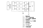
本実施形態の半導体装置の構成について、図1、7、及び15を参照して説明する。図15に示すように、本発明の半導体装置20は、非接触でデータを交信する機能を有し、電源回路11、クロック発生回路12、データ復調/変調回路13、他の回路を制御する制御回路14、インターフェイス回路15、記憶回路16、データバス17、アンテナ(アンテナコイル)18を有する。
(Embodiment 1)
The configuration of the semiconductor device of this embodiment will be described with reference to FIGS. As shown in FIG. 15, the
電源回路11は、アンテナ18から入力された交流信号を基に、半導体装置20の内部の各回路に供給する各種電源を生成する回路である。クロック発生回路12は、アンテナ18から入力された交流信号を基に、半導体装置20の内部の各回路に供給する各種クロック信号を生成する回路である。データ復調/変調回路13は、リーダライタ19と交信するデータを復調/変調する機能を有する。制御回路14は、記憶回路16を制御する機能を有する。アンテナ18は、電磁界或いは電波の送受信を行う機能を有する。リーダライタ19は、半導体装置との交信、制御及びそのデータに関する処理を制御する。なお、半導体装置は上記構成に制約されず、例えば、電源電圧のリミッタ回路や暗号処理専用ハードウエアといった他の要素を追加した構成であってもよい。
The
記憶回路16は、一対の導電層間に有機化合物層又は相変化層が挟まれた記憶素子を有することを特徴とする。なお、記憶回路16は、一対の導電層間に有機化合物層又は相変化層が挟まれた記憶素子のみを有していてもよいし、他の構成の記憶回路を有していてもよい。他の構成の記憶回路とは、例えば、DRAM、SRAM、FeRAM、マスクROM、PROM、EPROM、EEPROM及びフラッシュメモリから選択される1つ又は複数に相当する。
The
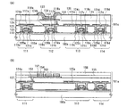
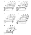
本実施形態の半導体装置20の斜視図について、図7(A)を用いて説明する。本実施形態の半導体装置は、図7(A)に示すように、基板上に複数の回路が集積された構成を有する。ここでは、基板100a上に複数のトランジスタを有する素子形成層101aが形成されており、複数のトランジスタを有する素子形成層101aは、代表的には複数のTFTを有する領域102、103と、記憶素子を有する領域104と、複数のTFTを有する領域102、103及び記憶素子を有する領域104の周囲に設けられたアンテナとして機能する導電層105とで構成されている。
A perspective view of the
なお、以下の実施形態では、複数のトランジスタを有する素子形成層は、TFTを有する領域102、103で構成されている例を示すが、TFTに限定されるものではなく、MOSトランジスタのように単結晶基板に形成されるトランジスタを用いて複数のトランジスタを有する素子形成層を形成することができる。この場合、基板100aは半導体単結晶基板となる。また、絶縁層と単結晶半導体層とが積層されたSOI(silicon on insulator)基板を用いることができる。さらには、有機半導体トランジスタを用いて複数のトランジスタを有する素子形成層を形成することができる。
In the following embodiments, an example in which the element formation layer having a plurality of transistors is configured by the
複数のTFTを有する領域102、103は様々な回路を構成する。複数のTFTを有する領域102の代表例としては、電源回路、クロック発生回路、データ復調/変調回路等のアンテナが受信する電磁波を処理する通信回路が設けられている。また、複数のTFTを有する領域103の代表例としては、他の回路を制御する制御回路、インターフェイス回路等を有する。
The
また、アンテナとして機能する導電層105は、通信回路を構成する複数のTFTを含む領域102と接続する。
In addition, the
また、記憶素子を含む領域104は、データを記憶する記憶回路を構成し、記憶素子及び当該記憶素子を動作させる回路等を有する。記憶素子を含む領域104は、制御回路、インターフェイス回路等を構成する複数のTFTを有する領域103と接続される。
The
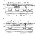
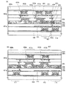
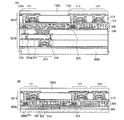
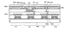
次に、図7(A)に示す構成を有する半導体装置の断面構造について、図1(A)を用いて説明する。基板100a上に複数のトランジスタを有する素子形成層101aが形成されている。ここでは、複数のトランジスタを有する素子形成層101aとして、記憶素子を動作させる回路を構成するTFT111(図7(A)の記憶素子を有する領域104の一部)、記憶素子のスイッチング用のTFT112(図7(A)の記憶素子を有する領域104の一部)、電源回路、クロック発生回路、データ復調/変調回路等のアンテナで受信した信号を処理する回路を構成するTFT113(図7(A)の複数のTFTを有する領域102の一部)、制御回路、インターフェイス等の回路を構成するTFT114(図7(A)の複数のTFTを有する領域103の一部)を示す。
Next, a cross-sectional structure of the semiconductor device having the structure illustrated in FIG. 7A will be described with reference to FIG. An
これらのTFTは、pチャネル型TFT、nチャネル型TFT等を適宜組み合わせて構成することが可能である。ここでは、それぞれの回路を構成するTFTをnチャネル型TFTで示す。 These TFTs can be configured by appropriately combining p-channel TFTs, n-channel TFTs, and the like. Here, TFTs constituting each circuit are shown as n-channel TFTs.
TFT111〜114は、基板100a上に絶縁層115を介して設けられている。TFTは、半導体領域、ゲート絶縁膜116a〜116d、ゲート電極117a〜117d、ゲート電極の側壁に設けられたサイドウォール118a〜118dで構成される。半導体層は、ソース領域及びドレイン領域119a〜119d、低濃度不純物領域120a〜120d、チャネル形成領域121a〜121dで構成される。また、低濃度不純物領域120a〜120dは、サイドウォール118a〜118dに覆われている。また、TFT111〜114を覆う絶縁層122が形成されている。絶縁層122は、パッシベーション膜として機能し、外部からの不純物、代表的にはアルカリ金等の汚染物質をブロックする効果があり、TFTが汚染されることがなく、信頼性が向上したTFT111〜114を提供することができる。なお、パッシベーション膜としては、窒化珪素膜、窒化酸化珪素膜又は酸化窒化珪素膜等が挙げられる。
The
なお、TFT111〜114の半導体層は、非晶質半導体、微結晶半導体、多結晶半導体、有機半導体等のいずれの半導体を活性層として用いてもよいが、良好な特性のトランジスタを得るために、金属元素を触媒として結晶化した半導体層、レーザ照射法により結晶化した半導体層を用いるとよい。また、プラズマCVD法により、SiH4/F2ガス、SiH4/H2ガス(Arガス)を用いて形成した半導体層や、前記半導体層にレーザ照射を行ったものを半導体層として用いるとよい。
Note that the semiconductor layer of the
また、TFT111〜114は、200度から600度の温度(好適には350度から550度)で結晶化した結晶質半導体層(低温ポリシリコン層)や、600度以上の温度で結晶化した結晶質半導体層(高温ポリシリコン層)を用いることができる。なお、基板上に高温ポリシリコン層を作成する場合は、ガラス基板では熱に脆弱な場合があるので、石英基板を使用するとよい。TFT111〜114の半導体層(特にチャネル形成領域)には、1×10¹⁹atoms/cm3〜1×1022atoms/cm3の濃度、好適には1×1019atoms/cm3〜5×1020atoms/cm3の濃度で、水素又はハロゲン元素を添加するとよい。そうすると、欠陥が少なく、クラックが生じにくい活性層を得ることができる。
The
また、TFT111〜114の半導体層の厚さは、20nm〜200nm、好ましくは40nm〜170nm、さらに好ましくは45nm〜55nm、さらに好ましくは50nmとするとよい。そうすると、折り曲げても、クラックが生じにくい素子形成層101aを提供することができる。
The thickness of the semiconductor layer of the
また、TFT111〜114の半導体層を構成する結晶は、キャリアの流れる方向(チャネル長方向)と平行に延びる結晶粒界を有するように形成するとよい。また、TFT111〜114のS値(サブスレッシュホールド値)は0.35V/sec以下(好ましくは0.09〜0.25V/sec)、移動度10cm2/Vs以上の特性を有するとよい。このような半導体層は、連続発振レーザや、10MHz以上、好ましくは60〜100MHzで動作するパルスレーザを半導体層に照射して形成することが可能である。
In addition, crystals constituting the semiconductor layers of the
低濃度不純物領域やソース領域及びドレイン領域には、p型又はn型の導電型を付与する元素が添加されている。ここでは、ソース領域及びドレイン領域119a〜119d及び低濃度不純物領域120a〜120dには、n型の導電型を付与する不純物元素を、イオン注入法やイオンドープ法で自己整合的に添加して形成することができる。
An element imparting p-type or n-type conductivity is added to the low-concentration impurity region, the source region, and the drain region. Here, the source and
なお、ここでは、TFT111〜114が低濃度不純物領域120a〜120dやサイドウォール118a〜118dを有する構成を示すが、本発明はこの構成に制約されない。必要がなければ低濃度不純物領域やサイドウォールは設けなくてもよい。
Note that here, a configuration in which the
また、半導体層として、公知の有機半導体材料を適宜用いることができる。代表例としては、骨格が共役二重結合から構成されるπ電子共役系の高分子材料が望ましい。代表的には、ポリチオフェン、ポリ(3−アルキルチオフェン)、ポリチオフェン誘導体、ペンタセン等の可溶性の高分子材料を用いることができる。 Moreover, a well-known organic-semiconductor material can be used suitably as a semiconductor layer. As a typical example, a π-electron conjugated polymer material whose skeleton is composed of conjugated double bonds is desirable. Typically, a soluble polymer material such as polythiophene, poly (3-alkylthiophene), a polythiophene derivative, or pentacene can be used.
その他にも、可溶性の前駆体を成膜した後で処理することにより半導体層を形成することができる。なお、このような前駆体を経由する有機半導体材料としては、ポリチエニレンビニレン、ポリ(2,5−チエニレンビニレン)、ポリアセチレン、ポリアセチレン誘導体、ポリアリレンビニレンなどがある。 In addition, a semiconductor layer can be formed by processing after forming a soluble precursor. Examples of the organic semiconductor material that passes through such a precursor include polythienylene vinylene, poly (2,5-thienylene vinylene), polyacetylene, a polyacetylene derivative, and polyarylene vinylene.
前駆体を有機半導体に変換する際には、加熱処理だけではなく塩化水素ガスなどの反応触媒を添加することがなされる。また、これらの可溶性有機半導体材料を溶解させる代表的な溶媒としては、トルエン、キシレン、クロロベンゼン、ジクロロベンゼン、アニソール、クロロホルム、ジクロロメタン、γブチルラクトン、ブチルセルソルブ、シクロヘキサン、NMP(N−メチル−2−ピロリドン)、シクロヘキサノン、2−ブタノン、ジオキサン、ジメチルホルムアミド(DMF)または、THF(テトラヒドロフラン)などを適用することができる。 When converting the precursor into an organic semiconductor, a reaction catalyst such as hydrogen chloride gas is added as well as heat treatment. Typical solvents for dissolving these soluble organic semiconductor materials include toluene, xylene, chlorobenzene, dichlorobenzene, anisole, chloroform, dichloromethane, γ-butyllactone, butyl cellosolve, cyclohexane, NMP (N-methyl-2 -Pyrrolidone), cyclohexanone, 2-butanone, dioxane, dimethylformamide (DMF), THF (tetrahydrofuran), or the like can be applied.
また、TFT111〜114と、パッシベーション膜として機能する絶縁層122を覆うように、絶縁層123が設けられており、これらの絶縁層123は、表面を平坦化するために設けられている。ソース配線又はドレイン配線として機能する導電層124a〜124dは、ソース領域及びドレイン領域119a〜119dに接し、絶縁層122、123に設けられたコンタクトホールを充填する。また、ソース配線又はドレイン配線として機能する導電層124a〜124dと同時に形成された層で、アンテナとしとして機能する導電層125aが形成される。導電層125aは、TFT113のソース配線又はドレイン配線として機能する導電層124cに接続する。導電層124a〜124d、125を覆うように、絶縁層126、127が設けられている。これらの絶縁層126、127は、表面を平坦化する目的と、TFT111〜114及び導電層124a〜124d、125を保護する目的で設けられている。
In addition, an insulating
また、TFT111〜114において、少なくともTFT113 、114は、リングオシレータ(9段インバータ)レベルで1MHz以上、好適には10MHz以上(3〜5Vにて)の特性を有する。又は、ゲートあたりの周波数特性を100kHz以上、好適には1MHz以上(3〜5Vにて)を有する。
In the
なお、後述するが、TFT111〜114上に積層する記憶素子134は、その構造によっては、レーザ光を用いた光学的作用によりデータの書き込みを行う。その場合、レーザ光から、TFT111〜114を保護するために、絶縁層127、及び後に形成される絶縁層135を遮光性がある絶縁性材料により形成する。遮光性がある絶縁性材料とは、例えば、公知の絶縁性材料に、カーボン粒子、金属粒子、顔料や着色料等を添加して撹拌した後、必要に応じて濾過を行った材料、又は、カーボン粒子等が均一に混合されるように、界面活性剤や分散剤を添加した材料等である。このような絶縁性材料は、スピンコート法で形成するとよい。
Note that, as will be described later, depending on the structure of the
また、絶縁層127上に記憶素子134が設けられている。記憶素子は、TFT112の一部又は全部に重畳することを特徴とする。当該構造により、狭い面積の半導体装置に記憶素子を高い密度で集積することが可能である。
In addition, the
絶縁層127上に、第1の導電層131、有機化合物層又は相変化層132、第2の導電層133が順に積層されており、この積層体が記憶素子134に相当する。隣接する有機化合物層又は相変化層132の間には、絶縁層135が設けられている。第1の導電層131は、TFT112のソース配線又はドレイン配線として機能する導電層124bと接続する。第2の導電層133上には、絶縁層136が設けられている。なお、TFT112は記憶素子のスイッチング用のTFTとして機能する。
A first
次に、図1(A)の各記憶素子にスイッチング用のTFTが設けられた記憶回路、即ちアクティブマトリクス型の記憶回路を有する半導体装置の代わりに、パッシブ型の記憶回路を有する半導体装置の断面構造について、図1(B)を用いて説明する。より詳しくは、図1(A)に示した半導体装置と比較すると、記憶素子134の構造及びそれに接続されるTFTが異なる半導体装置の断面構造について説明する。
Next, a cross section of a semiconductor device having a passive memory circuit instead of a memory circuit in which a switching TFT is provided in each memory element in FIG. 1A, that is, a semiconductor device having an active matrix memory circuit. The structure will be described with reference to FIG. More specifically, a cross-sectional structure of a semiconductor device in which the structure of the
絶縁層127上に、TFT111のソース配線又はドレイン配線として機能する導電層124aに接続するように、第1の導電層151が設けられ、第1の導電層151に接するように有機化合物層又は相変化層152が設けられ、有機化合物層又は相変化層152に接するように第2の導電層153が設けられている。第1の導電層151と、有機化合物層又は相変化層152と、第2の導電層153との積層体が記憶素子154に相当する。隣接する有機化合物層又は相変化層152の間には、絶縁層155が設けられている。記憶素子154上には、絶縁層156が設けられている。
A first
なお、第1の導電層151は共通電極として機能し、第1の導電層151を用いて複数の記憶素子154が形成される。
Note that the first
図1(B)に示す記憶素子154は、各記憶素子154にスイッチング用のTFTが接続されておらず、記憶素子を動作させる回路を構成するTFT111に直接接続される。
In the
また、図1(A)及び(B)においては、基板上に複数のトランジスタを有する素子形成層101aが形成された半導体装置の断面図について説明しているが、これに限定されない。例えば、基板上に剥離層を設け、剥離層上に複数のトランジスタを有する素子形成層101aを形成した後、複数のトランジスタを有する素子形成層101aを剥離層から剥離し、図2(A)に示すように、基板200a上に接着層201を介して複数のトランジスタを有する素子形成層101aを貼り合わせても良い。なお剥離方法としては、(1)基板と複数のトランジスタを有する素子形成層の間に金属酸化膜を設け、当該金属酸化膜を結晶化により脆弱化して、当該複数のトランジスタを有する素子形成層を物理的に剥離する方法、(2)基板と複数のトランジスタを有する素子形成層の間に水素を含む非晶質珪素膜を設け、レーザ光の照射またはエッチングにより当該非晶質珪素膜を除去することで、当該複数のトランジスタを有する素子形成層を剥離する方法、(3)複数のトランジスタを有する素子形成層が形成された基板を機械的に削除する、又は溶液によるエッチングで除去する方法、(4)基板と複数のトランジスタを有する素子形成層の間に剥離層及び金属酸化膜を設け、当該金属酸化膜を結晶化により脆弱化し、剥離層の一部を溶液やCF3等のガスによるエッチングで除去した後、脆弱化された金属酸化膜において物理的に剥離する方法等を用いればよい。
1A and 1B illustrate a cross-sectional view of a semiconductor device in which an
また、基板200aとしては、可撓性があり、薄くて軽いプラスチック基板を用いることが好ましく、具体的には、PET(ポリエチレンテレフタレート)、PEN(ポリエチレンナフタレート)、PES(ポリエーテルスルホン)、ポリプロピレン、ポリプロピレンサルファイド、ポリカーボネート、ポリエーテルイミド、ポリフェニレンサルファイド、ポリフェニレンオキサイド、ポリサルフォン、ポリフタールアミド等からなる基板を用いることができる。また、ラミネートフィルム(ポリプロピレン、ポリエステル、ビニル、ポリフッ化ビニル、塩化ビニルなどからなる)、繊維質な材料からなる紙、基材フィルム(ポリエステル、ポリアミド、無機蒸着フィルム、紙類等)と接着性合成樹脂フィルム(アクリル系合成樹脂、エポキシ系合成樹脂等)との積層フィルムなどを用いることもできる。
The
ラミネートフィルムは、熱圧着により、被処理体と封止処理が行われるものであり、封止処理を行う際には、ラミネートフィルムの最表面に設けられた接着層か、又は最外層に設けられた層(接着層ではない)を加熱処理によって溶かし、加圧により接着する。基板200aの表面には接着層が設けられていてもよいし、接着層が設けられていなくてもよい。
The laminate film is subjected to sealing treatment with the object to be processed by thermocompression bonding. When the sealing treatment is performed, the laminate film is provided on the outermost layer of the laminate film or on the outermost layer. The layer (not the adhesive layer) is melted by heat treatment and bonded by pressure. An adhesive layer may be provided on the surface of the
接着層201は、熱硬化樹脂、紫外線硬化樹脂、エポキシ樹脂系接着剤、樹脂添加剤等の接着剤を含む層である。
The
上記のように、剥離した複数のトランジスタを有する素子形成層101aを、可撓性があり、薄くて軽いプラスチック基板に貼り合わせると、厚さが薄く、軽く、落下しても割れにくい半導体装置を提供することができる。また、曲面や異形の形状上に貼り合わせることが可能となり、多種多様の用途が実現する。例えば、薬の瓶のような曲面上に、本発明の半導体装置を密着して貼り合わせることができる。さらに、基板を再利用すれば、安価な半導体装置の提供を実現する。
As described above, when the
また、図2(B)に示すように、記憶素子134の第1の導電層131と同時に形成された導電層で、アンテナとして機能する導電層215aを形成してもよい。このとき、アンテナとして機能する導電層215は、ソース配線又はドレイン配線として機能する導電層124cと接続する。
Alternatively, as illustrated in FIG. 2B, a
更には、図2(C)に示すように、記憶素子134の第2の導電層133と同時に形成された導電層で、アンテナとして機能する導電層225aを形成してもよい。このとき、アンテナとして機能する導電層225aは、導電層214を介してソース配線又はドレイン配線として機能する導電層124cと接続する。
Further, as illustrated in FIG. 2C, a
なお、図2(A)〜(C)に示す半導体装置は、図1(B)に示すような、スイッチング用のTFTが各記憶素子に設けられていない記憶素子を有するパッシブマトリクス型の記憶回路を有する半導体装置にも適応することが可能である。 Note that the semiconductor device illustrated in FIGS. 2A to 2C includes a passive matrix memory circuit including a memory element in which a switching TFT is not provided in each memory element as illustrated in FIG. It is also possible to apply to a semiconductor device having
本発明の半導体装置は、複数のTFTを有する素子形成層上に、記憶素子を積層した構成を有することを特徴とし、上記特徴により、小型の半導体装置を提供することができる。また、TFTのソース配線又はドレイン配線、記憶素子の導電層の何れかと同時に、アンテナとして機能する導電層を形成するため、工程数を削減することが可能であり、スループットを向上させることが可能である。 The semiconductor device of the present invention has a structure in which a memory element is stacked over an element formation layer having a plurality of TFTs. With the above characteristics, a small semiconductor device can be provided. In addition, since the conductive layer functioning as an antenna is formed at the same time as the source wiring or drain wiring of the TFT or the conductive layer of the memory element, the number of steps can be reduced and throughput can be improved. is there.
上記構成を有する半導体装置において、記憶素子は、一対の導電層(第1の導電層と第2の導電層)間に有機化合物層又は相変化層が挟まれた単純な構造を有することを特徴とする。上記特徴により、作製が簡単であるために安価な半導体装置及びその作製方法を提供することができる。また、高集積化が容易なため、大容量の記憶回路を有する半導体装置及びその作製方法を提供することができる。 In the semiconductor device having the above structure, the memory element has a simple structure in which an organic compound layer or a phase change layer is sandwiched between a pair of conductive layers (a first conductive layer and a second conductive layer). And With the above characteristics, since the manufacturing is simple, an inexpensive semiconductor device and a manufacturing method thereof can be provided. In addition, since high integration is easy, a semiconductor device having a large-capacity memory circuit and a manufacturing method thereof can be provided.
また、本発明の半導体装置が含む記憶回路は、光学的作用又は電気的作用によりデータの書き込みを行うものであり、不揮発性であって、データの追記が可能であることを特徴とする。上記特徴により、書き換えによる偽造を防止することができ、新たなデータを追加して書き込むことができる。従って、高機能化と高付加価値化を実現した半導体装置及びその作製方法を提供することができる。 Further, a memory circuit included in the semiconductor device of the present invention writes data by an optical action or an electrical action, is nonvolatile, and can additionally write data. With the above feature, forgery due to rewriting can be prevented, and new data can be added and written. Accordingly, it is possible to provide a semiconductor device that achieves high functionality and high added value and a manufacturing method thereof.
(実施形態2)
本実施形態では、上記実施形態とは異なる本発明の半導体装置の構成について、図3、7を参照して説明する。
(Embodiment 2)
In this embodiment mode, a structure of a semiconductor device of the present invention which is different from that of the above embodiment mode will be described with reference to FIGS.
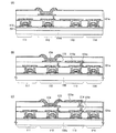
本実施形態の半導体装置は、図7(B)に示すように、第1の基板100a上に形成された複数のトランジスタを有する素子形成層301aと、第2の基板300a上に形成されたアンテナとして機能する導電層105を有する素子形成層302aとが、接着層で貼り合わせられた構成を有する。
As shown in FIG. 7B, the semiconductor device of this embodiment includes an
ここでは、複数のトランジスタを有する素子形成層301aは、代表的には複数のTFTを有する領域102、103と、記憶素子を有する領域104で構成される。また、素子形成層302aに形成されるアンテナとして機能する導電層105は、素子形成層301aに形成される通信回路を構成する複数のTFTを有する領域102と、図示しないが導電性粒子で接続されている。
Here, the
上記の図7(B)に示す構成を有する本発明の半導体装置の断面構造について、図3を用いて説明する。 A cross-sectional structure of the semiconductor device of the present invention having the structure shown in FIG. 7B is described with reference to FIG.
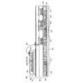
図3(A)に示すように、本実施形態の半導体装置は、第1の基板100a上に形成された複数のトランジスタと記憶素子を有する素子形成層301aと、第2の基板300a上に形成されたアンテナとして機能する導電層303aを有する素子形成層302aとが、接着層306で貼り合わせられた構成を有する。
As shown in FIG. 3A, the semiconductor device of this embodiment is formed on the
複数のTFTと記憶素子を有する素子形成層301aは、TFT111〜114を有する。これらのTFT111〜114の構造は上述した通りであり、また、記憶素子134は、図1(A)に示す記憶素子134と同じ構造を用いて形成することが可能であり、TFT112の一部又は全部に重畳することにより、狭い面積の半導体装置に記憶素子を高い密度で集積することが可能である。
The
基板100aに形成された、複数のTFT111〜114及び記憶素子134を有する素子形成層301aと、基板300aに形成された導電層303を有する素子形成層302aは、導電性粒子305を含む接着層306により貼り合わせられている。また、TFT113のソース配線又はドレイン配線として機能する導電層124cは、導電層214を介して、導電層224に接続される。導電層224は接続端子として機能する。また、導電層214は、記憶素子134の第1の導電層131と同時に形成される導電層である。また、導電層224は、記憶素子134の第2の導電層133と同時に形成される導電層である。さらに、接続端子として機能する導電層224と、アンテナとして機能する導電層303とは、導電性粒子305を介して電気的に接続されている。
An
なお、アンテナとして機能する導電層303が設けられた第2の基板300aは、基板200aと同様の基板を用いることが可能である。また、基板300a及び導電層303表面に絶縁層307を形成しても良い。ただし、TFT113の接続端子として機能する導電層224と接続する領域は、導電層303が露出されている。
Note that the
接着層306は、熱硬化樹脂、紫外線硬化樹脂、エポキシ樹脂系接着剤、樹脂添加剤等の接着剤を含み、導電性粒子305が分散されている。このような接着剤を異方性導電接着剤という。導電性粒子305は、金、銀、銅、パラジウム、又は白金から選ばれた一元素、若しくは複数の元素で形成される。また、これらの元素の多層構造を有する粒子でも良い。導電性粒子305は、直径が1〜100nm、好ましくは5〜50nmである場合、一つ又は複数の導電性粒子305と導電層303、224が接続する。この場合、一つ又は複数の導電性粒子305で導電層303と導電層224の間隔を保持する。
The
また、図37に示すように、直径が0.5〜10μm、好ましくは1〜5μmの導電性粒子308が含まれる接着層306を用いても良い。この場合、導電層303と導電層224は、垂直方向に押しつぶされた形状の導電性粒子309で接続される。このときは、押しつぶされた導電性粒子309で導電層303と導電層224の間隔を保持する。
As shown in FIG. 37, an
また、樹脂で形成された粒子の表面に、金、銀、銅、パラジウム、又は白金から選ばれた一元素、若しくは複数の元素で形成される薄膜が形成された導電性粒子を用いてもよい。さらには、異方性導電接着剤の代わりに、ベースフィルム上にフィルム状に形成された異方性導電フィルムを転写して用いても良い。異方性導電フィルムも、異方性導電接着剤と同様の導電性粒子が分散されている。 Alternatively, conductive particles in which a thin film formed of one element selected from gold, silver, copper, palladium, or platinum or a plurality of elements may be used on the surface of particles formed of resin. . Furthermore, instead of the anisotropic conductive adhesive, an anisotropic conductive film formed in a film shape on the base film may be transferred and used. In the anisotropic conductive film, conductive particles similar to the anisotropic conductive adhesive are dispersed.
図3(A)に示す記憶素子134は、スイッチング用のTFT112が、各記憶素子134に設けられている。即ち、アクティブマトリクス型の記憶回路を有する半導体装置である。なお、図3(B)に示すように、第1の導電層151、有機化合物層又は相変化層152、第2の導電層153で構成される記憶素子154を設けることも可能である。この構造では、図1(B)と同様に記憶素子154には各スイッチング用のTFTが接続されておらず、TFT111に直接接続されている。また、第1の導電層151は共通電極として機能し、第1の導電層151を用いて複数の記憶素子154が形成されており、パッシブマトリクス型の記憶回路を有する半導体装置である。
In the
さらには、本実施形態においても、図2(A)に示すように、接着層201を介して基板200a上に複数のトランジスタを有する素子形成層301aを設けても良い。
Furthermore, also in this embodiment, as illustrated in FIG. 2A, an
本発明の半導体装置は、複数のTFTを有する素子形成層上に、記憶素子を含む層を積層した構成を有することを特徴とし、上記特徴により、小型の半導体装置を提供することができる。また、複数のトランジスタと記憶素子を有する素子形成層を形成する工程とアンテナとして機能する導電層を形成する工程を、独立に並行して行うことができる。従って、本発明は短時間で効率よく半導体装置を作製することができる。また、複数のトランジスタを有する素子形成層や、アンテナそれぞれが形成された時点で、各回路の性能を確認し、選別して、複数のトランジスタを有する素子形成層や、アンテナを電気的に接続させ半導体装置を完成させることができる。従って、欠陥品が作製される割合を抑えることができ、歩留まりを改善することができる。 The semiconductor device of the present invention has a structure in which a layer including a memory element is stacked over an element formation layer having a plurality of TFTs. With the above characteristics, a small semiconductor device can be provided. In addition, the step of forming an element formation layer having a plurality of transistors and memory elements and the step of forming a conductive layer functioning as an antenna can be performed independently and in parallel. Therefore, the present invention can manufacture a semiconductor device efficiently in a short time. In addition, when each of the element formation layers having a plurality of transistors and the antennas are formed, the performance of each circuit is confirmed and selected to electrically connect the element formation layers having a plurality of transistors and the antennas. A semiconductor device can be completed. Therefore, the rate at which defective products are produced can be suppressed, and the yield can be improved.
(実施形態3)
本実施形態では、上記実施形態の構成とは異なる本発明の半導体装置の断面構造について、図4及び図7を用いて説明する。より詳しくは、図3に示した半導体装置と比較すると、アンテナを有する導電層の代わりに、記憶素子を有する素子形成層402aが形成された基板が貼り合わせられた構造の半導体装置の断面構造について説明する。
(Embodiment 3)
In this embodiment, a cross-sectional structure of a semiconductor device of the present invention, which is different from the structure of the above embodiment, will be described with reference to FIGS. More specifically, as compared with the semiconductor device illustrated in FIGS. 3A and 3B, a cross-sectional structure of a semiconductor device in which a substrate on which an
本実施形態の半導体装置は、図7(C)に示すように、第1の基板100a上に形成された複数のトランジスタを有する素子形成層401aと、第2の基板400a上に形成された記憶素子を有する素子形成層402aとが、接着層で貼り合わせられた構成を有する。
As shown in FIG. 7C, the semiconductor device of this embodiment includes an
ここでは、複数のトランジスタを有する素子形成層401aは、代表的には複数のTFTを有する領域102、103と、アンテナとして機能する導電層125aを有する。また、記憶素子を有する素子形成層402aは、記憶素子を有する領域104で構成される。また、記憶素子を有する領域104は、制御回路、インターフェイス等を構成する複数のTFTを含む領域103と、図示しないが導電性粒子で接続されている。
Here, the
上記の図7(C)に示す構成を有する本発明の半導体装置の断面構造について、図4を用いて説明する。 A cross-sectional structure of the semiconductor device of the present invention having the structure shown in FIG. 7C is described with reference to FIGS.
図4(A)に示すように、基板100a上には、アンテナとして機能する導電層及び複数のトランジスタを有する素子形成層401aが形成され、アンテナとして機能する導電層及び複数のトランジスタを有する素子形成層401aはTFT111、113、114を有し、これらのTFTの構造は上述した通りである。また、基板400a上に記憶素子を有する素子形成層402aが形成されている。図4(A)においては、記憶素子434a、434bそれぞれに、スイッチング用のTFT412a、412bが接続されている。即ち、スイッチング用のTFT412a、412bのソース配線又はドレイン配線の一方に記憶素子の第1の導電層431a、431bが接続されている。また、スイッチング用のTFT412a、412bのソース配線又はドレイン配線の他方は、記憶素子の第1の導電層又は第2の導電層と同時に形成された導電層と接続されている。ここでは、ソース配線又はドレイン配線として機能する導電層424の他方は、導電層425を介して導電層426と接続している。なお、導電層425は、記憶素子の第1の導電層431a、431bと同時に形成された導電層であり、導電層426は、記憶素子の第2の導電層433a、433bと同時に形成された導電層である。
As shown in FIG. 4A, an
また、複数のトランジスタを有する素子形成層401a及び記憶素子を有する素子形成層402aが接着層306で接着されている。
In addition, an
また、記憶素子のスイッチング用のTFT412aのソース配線又はドレイン配線として機能する導電層424と、記憶素子を動作させる回路を構成するTFT111のソース配線又はドレイン配線として機能する導電層124aとは、導電性粒子305、及び導電層421、425、426を介して電気的に接続されている。
The
なお、記憶素子の構成によっては、記憶素子を有する素子形成層402aに対して、レーザ光を用いた光学的作用によりデータの書き込みを行う場合がある。そのような場合、記憶素子を有する素子形成層402aにおいて、スイッチング用のTFT412a、412bと、記憶素子434a、434bそれぞれが、重ならない領域を有するようにレイアウトをすることが必要である。
Note that depending on the structure of the memory element, data may be written to the
図4(A)に示す記憶素子434a、434bは、それぞれスイッチング用のTFT412a、412bに接続される。即ち、アクティブマトリクス型の半導体装置である。なお、図4(B)に示すように、第1の導電層451、有機化合物層又は相変化層452、第2の導電層453で構成される記憶素子454を有する基板を貼り合わせることも可能である。また、第1の導電層451、有機化合物層又は相変化層452、第2の導電層453は、それぞれ実施形態1に示す第1の導電層151と、有機化合物層又は相変化層152と、第2の導電層153と同様の構造を用いることができる。この構造では、図1(B)と同様に記憶素子454には各スイッチング用のTFTが接続されておらず、記憶素子を動作させる回路を構成するTFT111に導電性粒子305を介して接続されている。また、第1の導電層451は共通電極として機能し、第1の導電層451を用いて複数の記憶素子454が形成されており、パッシブマトリクス型の記憶回路を有する半導体装置である。
また、上記実施形態において、複数のトランジスタを有する素子形成層401aに記憶素子を動作させる回路が形成されるが、これに限定されるものではない。例えば、記憶素子を有する素子形成層402aに記憶素子を動作させる回路が形成されてもよい。具体的には、図8(A)に示すように、記憶素子434a、434bとともに、記憶素子を動作させる回路を構成するTFT811を基板400a上に形成した後、記憶素子を有する素子形成層402aと複数のトランジスタを有する素子形成層401aと、導電性粒子305を有する接着層306で貼り合わせてもよい。このとき、記憶素子を動作させる回路を構成するTFT811のソース配線又はドレイン配線として機能する導電層424の一方と、TFT114のソース配線又はドレイン配線として機能する導電層124aの一方とが、導電性粒子305、及び導電層825、826、827を介して電気的に接続される。なお、導電層826は、TFT811のソース配線又はドレイン配線として機能する導電層424の一方と導電層825を介して接続されている。また、導電層826は、記憶素子の第2の導電層と同時に形成された導電層であり、導電層825は、記憶素子の第1の導電層と同時に形成された導電層である。
In the above embodiment, a circuit for operating a memory element is formed in the
また、図4(A)において、記憶素子を有する素子形成層402aは基板400a上に形成された構造を有しているが、図8(B)に示すように、基板800a上に接着層834を介して記憶素子を有する素子形成層402aを貼り合せても良い。
4A, the
本発明の半導体装置は、アンテナとして機能する導電層と複数のトランジスタを有する素子形成層上に、記憶素子を含む層を貼りあわせた構成を有することを特徴とし、上記特徴により、小型の半導体装置を提供することができる。また、複数のトランジスタを有する素子形成層を形成する工程と、記憶素子を有する素子形成層を形成する工程を、独立に並行して行うことができる。従って、本発明は短時間で効率よく半導体装置を作製することができる。また、複数のトランジスタを有する素子形成層や、記憶素子それぞれが形成された時点で、それぞれの性能を確認し、選別して、複数のトランジスタを有する素子形成層や記憶素子を電気的に接続させ半導体装置を完成させることができる。従って、欠陥品が作製される割合を抑えることができ、歩留まりを改善することができる。 The semiconductor device of the present invention has a structure in which a layer including a memory element is bonded to an element formation layer having a plurality of transistors and a conductive layer that functions as an antenna. Can be provided. In addition, the step of forming an element formation layer having a plurality of transistors and the step of forming an element formation layer having a memory element can be performed independently and in parallel. Therefore, the present invention can manufacture a semiconductor device efficiently in a short time. In addition, when each of the element formation layer having a plurality of transistors and the memory element is formed, the performance of each element is confirmed and selected, and the element formation layer having a plurality of transistors and the memory element are electrically connected. A semiconductor device can be completed. Therefore, the rate at which defective products are produced can be suppressed, and the yield can be improved.
(実施形態4)
本実施形態では、上記実施形態の構成とは異なる本発明の半導体装置の断面構造について説明する。より詳しくは、複数のトランジスタを有する素子形成層に、記憶素子及びアンテナが形成された層を有する基板が貼り合わせられた構造の半導体装置の断面構造について、図5及び図7を用いて説明する。
(Embodiment 4)
In this embodiment, a cross-sectional structure of the semiconductor device of the present invention, which is different from the structure of the above embodiment, will be described. More specifically, a cross-sectional structure of a semiconductor device in which a substrate including a layer including a memory element and an antenna is bonded to an element formation layer including a plurality of transistors will be described with reference to FIGS. .
本実施形態の半導体装置は、図7(D)に示すように、第1の基板100a上に形成された複数のトランジスタを有する素子形成層501aと、第2の基板500a上に形成された記憶素子及びアンテナを有する素子形成層502aとが、接着層で貼り合わせられた構成を有する。
As shown in FIG. 7D, the semiconductor device of this embodiment includes an
ここでは、複数のトランジスタを有する素子形成層501aは、代表的には複数のTFTを有する領域102、103を有する。また、記憶素子及びアンテナを有する素子形成層502aは、記憶素子を有する領域104及びアンテナとして機能する導電層105で構成される。また、記憶素子を有する領域104は、制御回路、インターフェイス等を構成する複数のTFTを含む領域103と、図示しないが導電性粒子で接続されている。また、及びアンテナとして機能する導電層105は、通信回路を構成する複数のTFTを含む領域102と、図示しないが導電性粒子で接続されている。
Here, the
上記の図7(D)に示す構成を有する本発明の半導体装置の断面構造について、図5を用いて説明する。 A cross-sectional structure of the semiconductor device of the present invention having the structure shown in FIG. 7D is described with reference to FIGS.
図5(A)に示すように、複数のTFTを有する素子形成層501aは、TFT111、113、114を有し、これらのTFTの構造は上述した通りである。また、基板500a上に記憶素子434及びアンテナとして機能する導電層525を有する素子形成層502が形成されている。図5(A)においては、記憶素子434に、スイッチング用のTFT412が接続されている。即ち、スイッチング用のTFT412のソース配線又はドレイン配線の一方に、記憶素子434の第1の導電層が接続されている。
As shown in FIG. 5A, an
また、スイッチング用のTFT412のソース配線又はドレイン配線の他方は、記憶素子の第1の導電層又は第2の導電層と同時に形成された導電層425と接続されている。ここでは、ソース配線又はドレイン配線として機能する導電層424の他方は、導電層425を介して導電層426と接続している。なお、導電層426は、記憶素子434の第2の導電層と同時に形成された導電層であり、接続端子として機能する。
The other of the source wiring and the drain wiring of the switching
また、TFT412のソース配線又はドレイン配線として機能する導電層424及びTFT111のソース配線又はドレイン配線として機能する導電層124aは、導電層421、425、426及び導電性粒子305を介して電気的に接続されている。
Further, the
また、記憶素子434の第1の導電層又は第2の導電層と同時に、アンテナとして機能する導電層525が形成される。導電層525は、TFT113のソース配線又はドレイン配線として機能する導電層124cと、導電性粒子305及び導電層521を介して電気的に接続される。また、導電層521は、アンテナとして機能する導電層525と接続するための接続端子として機能する。
In addition, a
なお、記憶素子の構成によっては、記憶素子434に対して、レーザ光を用いた光学的作用によりデータの書き込みを行う場合がある。そのような場合、記憶素子及びアンテナを有する素子形成層502aにおいて、スイッチング用のTFT412及び記憶素子434、並びに導電層424及び記憶素子434が、重ならない領域を有するように、レイアウトをすることが必要である。
Note that depending on the structure of the memory element, data may be written to the
図5(A)に示す記憶素子434は、スイッチング用のTFT412に接続される。即ち、アクティブマトリクス型の半導体装置である。なお、図5(B)に示すように、第1の導電層451、有機化合物層又は相変化層452、第2の導電層453で構成される記憶素子454を有する基板500を貼り合わせることも可能である。また、第1の導電層451、有機化合物層又は相変化層452、第2の導電層453は、それぞれ実施形態1に示す第1の導電層151と、有機化合物層又は相変化層152と、第2の導電層153と同様の構造を用いることができる。この構造では、図1(B)と同様に、パッシブマトリクス型の記憶回路を有する半導体装置である。
A
また、複数のトランジスタを有する素子形成層501aに記憶素子を動作させる回路を構成するTFT111が形成されるが、この構造に限定されない。記憶素子及びアンテナを有する素子形成層に記憶素子を動作させる回路が形成されてもよい。また、図5(A)において、記憶素子及びアンテナを有する素子形成層502aは基板500a上に形成された構造を有しているが、基板上に接着層を介して記憶素子及びアンテナを有する素子形成層502aを貼り合せても良い。さらには、複数のトランジスタを有する素子形成層501aは基板100a上に形成されているが、図2(A)に示すように基板200a上に接着層を介して複数のトランジスタを有する素子形成層501aを貼り合せても良い。
In addition, the
本発明の半導体装置は、複数のTFTを有する素子形成層上に、記憶素子及びアンテナを含む素子形成層を接着層を介して積層した構成を有することを特徴とし、上記特徴により、小型の半導体装置を提供することができる。また、複数のトランジスタを有する素子形成層を形成する工程と、記憶素子及びアンテナを有する素子形成層を形成する工程を、独立に並行して行うことができる。従って、本発明は短時間で効率よく半導体装置を作製することができる。また、複数のトランジスタを有する素子形成層や、記憶素子、アンテナそれぞれが形成された時点で、それぞれの性能を確認し、選別して、複数のトランジスタを有する素子形成層や記憶素子、アンテナを電気的に接続させ半導体装置を完成させることができる。従って、欠陥品が作製される割合を抑えることができ、歩留まりを改善することができる。 A semiconductor device according to the present invention has a structure in which an element formation layer including a memory element and an antenna is stacked via an adhesive layer on an element formation layer having a plurality of TFTs. An apparatus can be provided. In addition, the step of forming an element formation layer having a plurality of transistors and the step of forming an element formation layer having a memory element and an antenna can be performed independently and in parallel. Therefore, the present invention can manufacture a semiconductor device efficiently in a short time. In addition, when each of the element formation layer having a plurality of transistors, the storage element, and the antenna is formed, the performance of each element is confirmed and selected to electrically connect the element formation layer, the storage element, and the antenna having a plurality of transistors. Thus, the semiconductor device can be completed. Therefore, the rate at which defective products are produced can be suppressed, and the yield can be improved.
(実施形態5)
本実施形態では、上記実施形態の構成とは異なる本発明の半導体装置の断面構造について説明する。より詳しくは、複数のトランジスタを有する素子形成層601aが形成される基板100a上に、記憶素子を有する素子形成層602aを搭載した構造の半導体装置の断面構造について、図6及び図7を用いて説明する。
(Embodiment 5)
In this embodiment, a cross-sectional structure of the semiconductor device of the present invention, which is different from the structure of the above embodiment, will be described. More specifically, a cross-sectional structure of a semiconductor device in which an
本実施形態の半導体装置は、図7(E)に示すように、基板100a上に形成された複数のトランジスタを有する素子形成層601aと基板100a上に、記憶素子を有する素子形成層602aが、接着層611で貼り合わせられた構成を有する。
As shown in FIG. 7E, the semiconductor device of this embodiment includes an
ここでは、複数のトランジスタを有する素子形成層601aは、代表的には複数のTFTを有する領域102、103及びアンテナとして機能する導電層105で構成される。また、記憶素子を有する素子形成層602aは、記憶素子を有する領域104で構成される。また、記憶素子を有する領域104は、制御回路、インターフェイス等を構成する複数のTFTを含む領域103と、導電部材631を用いて電気的に接続されている。
Here, the
上記の図7(E)に示す構成を有する本発明の半導体装置の断面構造について、図6を用いて説明する。 A cross-sectional structure of the semiconductor device of the present invention having the structure shown in FIG. 7E is described with reference to FIGS.
図6(A)に示すように、複数のTFTを有する素子形成層601aは、TFT111、113、114を有し、これらのTFTの構造は上述した通りである。また、記憶素子を有する素子形成層602aが形成された基板621aが、基板100a上に接着層611を用いて搭載されている。図6(A)においては、記憶素子634に、スイッチング用のTFT112が接続されている。即ち、スイッチング用のTFT112のソース配線又はドレイン配線の一方に、記憶素子の第1の導電層が接続されている。また、スイッチング用のTFT112のソース配線又はドレイン配線の他方は、記憶素子の第1の導電層又は第2の導電層と同時に形成された導電層と接続されている。ここでは、ソース配線又はドレイン配線として機能する導電層124bの他方は、導電層625を介して導電層626と接続している。なお、導電層625は、記憶素子の第1の導電層と同時に形成された導電層であり、導電層626は、記憶素子の第2の導電層と同時に形成された導電層であり、接続端子として機能する。
As shown in FIG. 6A, the
また、記憶素子を有する素子形成層602aに形成された記憶素子634のスイッチング用のTFT112と、複数のTFTを有する素子形成層601aに形成された記憶素子を動作させる回路を構成するTFT111とが、導電部材631で電気的に接続されている。ここでは、導電部材631をワイヤーを用い、ワイヤボンディング法によりTFT111とTFT112とを接続しているが、導電膜を成膜した後、所望の形状にエッチングして、導電部材631を形成してもよい。さらには、印刷法等の接続方法を用いることができる。
Further, a switching
図6(A)に示す記憶素子634は、スイッチング用のTFT112に接続される。即ち、アクティブマトリクス型の半導体装置である。なお、図6(B)に示すように、第1の導電層651、有機化合物層又は相変化層652、第2の導電層653で構成される記憶素子654が形成される基板622を、接着層611を用いて基板100a上に搭載することも可能である。この構造では、パッシブマトリクス型の記憶回路を有する半導体装置である。
A
また、本実施形態では、記憶素子を有する素子形成層602aを基板100a上に搭載したが、これに限定されず、記憶素子及びアンテナを有する素子形成層や、アンテナを有する素子形成層を基板100a上に搭載しても良い。
In this embodiment, the
本発明の半導体装置は、複数のTFTを有する素子形成層と、記憶素子を含む層を同一基板上に有することを特徴とし、上記特徴により、小型の半導体装置を提供することができる。また、複数のトランジスタを有する素子形成層を形成する工程と、記憶素子を有する素子形成層を形成する工程を、独立に並行して行うことができる。従って、本発明は短時間で効率よく半導体装置を作製することができる。また、複数のトランジスタを有する素子形成層や、記憶素子それぞれが形成された時点で、それぞれの性能を確認し、選別して、複数のトランジスタを有する素子形成層や記憶素子を電気的に接続させ半導体装置を完成させることができる。従って、欠陥品が作製される割合を抑えることができ、歩留まりを改善することができる。 The semiconductor device of the present invention includes an element formation layer having a plurality of TFTs and a layer including a memory element over the same substrate. With the above characteristics, a small semiconductor device can be provided. In addition, the step of forming an element formation layer having a plurality of transistors and the step of forming an element formation layer having a memory element can be performed independently and in parallel. Therefore, the present invention can manufacture a semiconductor device efficiently in a short time. In addition, when each of the element formation layer having a plurality of transistors and the memory element is formed, the performance of each element is confirmed and selected, and the element formation layer having a plurality of transistors and the memory element are electrically connected. A semiconductor device can be completed. Therefore, the rate at which defective products are produced can be suppressed, and the yield can be improved.
(実施形態6)
本実施形態では、半導体装置の作製方法に関して図面を参照して説明する。ここでは、実施形態1の図2(A)で示す半導体装置の作製方法を示すが、各実施形態に示される半導体装置にそれぞれ、本実施形態を適宜適応することが可能である。
(Embodiment 6)
In this embodiment, a method for manufacturing a semiconductor device will be described with reference to drawings. Here, a method for manufacturing the semiconductor device illustrated in FIG. 2A of
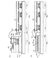
図9(A)に示すように、基板1100の一表面に、剥離層1101、1102を形成する。
As shown in FIG. 9A, release layers 1101 and 1102 are formed on one surface of a
基板1100は、ガラス基板、石英基板、金属基板やステンレス基板の一表面に絶縁層を形成したもの、本工程の処理温度に耐えうる耐熱性があるプラスチック基板等を用いる。上記に挙げた基板1100には、大きさや形状に制約がないため、例えば、基板1100として、1辺が1メートル以上であって、矩形状のものを用いれば、生産性を格段に向上させることができる。この利点は、円形のシリコン基板を用いる場合と比較すると、大きな優位点である。
As the
また、基板1100上に設けられる複数のトランジスタを有する素子形成層は、後に基板1100上から剥離される。従って、基板1100を再利用して、当該基板1100上に新たに複数のトランジスタを有する素子形成層を形成してもよい。この結果、コストを削減することができる。なお、再利用する基板1100には、石英基板を用いることが好ましい。
In addition, the element formation layer including a plurality of transistors provided over the
剥離層1101、1102は、基板1100の一表面に薄膜を形成した後、フォトリソグラフィ法により形成したレジストマスクを用いて選択的にエッチングして形成する。剥離層1101、1102は、スパッタリング法やプラズマCVD法等により、タングステン(W)、モリブデン(Mo)、チタン(Ti)、タンタル(Ta)、ニオブ(Nb)、ニッケル(Ni)、コバルト(Co)、ジルコニウム(Zr)、亜鉛(Zn)、ルテニウム(Ru)、ロジウム(Rh)、鉛(Pb)、オスミウム(Os)、イリジウム(Ir)、珪素(Si)から選択された元素、又は前記元素を主成分とする合金材料、又は前記元素を主成分とする化合物材料からなる層を、単層又は積層して形成する。珪素を含む層の結晶構造は、非晶質、微結晶、多結晶のいずれの場合でもよい。
The peeling layers 1101 and 1102 are formed by forming a thin film over one surface of the
剥離層1101、1102が単層構造の場合、好ましくは、タングステン層、モリブデン層、又はタングステンとモリブデンの混合物を含む層を形成する。又は、タングステンの酸化物若しくは酸化窒化物を含む層、モリブデンの酸化物若しくは酸化窒化物を含む層、又はタングステンとモリブデンの混合物の酸化物若しくは酸化窒化物を含む層を形成する。なお、タングステンとモリブデンの混合物とは、例えば、タングステンとモリブデンの合金に相当する。
In the case where the
剥離層1101、1102が積層構造の場合、好ましくは、1層目としてタングステン層、モリブデン層、又はタングステンとモリブデンの混合物を含む層を形成し、2層目として、タングステン、モリブデン又はタングステンとモリブデンの混合物の酸化物、窒化物、酸化窒化物又は窒化酸化物を形成する。
In the case where the
剥離層1101、1102として、タングステンを含む層とタングステンの酸化物を含む層の積層構造を形成する場合、タングステンを含む層を形成し、その上層に酸化珪素を含む層を形成することで、タングステン層と酸化珪素層との界面に、タングステンの酸化物を含む層が形成されることを活用してもよい。さらには、タングステンを含む層の表面を、熱酸化処理、酸素プラズマ処理、N2Oプラズマ処理、オゾン水等の酸化力の強い溶液での処理等を行ってタングステンの酸化物を含む層を形成してもよい。これは、タングステンの窒化物、酸化窒化物及び窒化酸化物を含む層を形成する場合も同様であり、タングステンを含む層を形成後、その上層に窒化珪素層、酸化窒化珪素層、窒化酸化珪素層を形成するとよい。
In the case where a stacked structure of a layer containing tungsten and a layer containing an oxide of tungsten is formed as the
タングステンの酸化物は、WOxで表される。Xは2≦X≦3の範囲内にあり、xが2の場合(WO2)、xが2.5の場合(W2O5)、xが2.75の場合(W4O11)、xが3の場合(WO3)などがある。タングステンの酸化物を形成するにあたり、上記に挙げたXの値に特に制約はなく、そのエッチングレートなどを基に決めるとよい。但し、エッチングレートの最も良いものは、酸素雰囲気下で、スパッタリング法により形成するタングステンの酸化物を含む層(WOx、0<X<3)である。従って、作製時間の短縮のために、剥離層として、酸素雰囲気下でスパッタリング法によりタングステンの酸化物を含む層を形成するとよい。 The oxide of tungsten is represented by WOx. X is in the range of 2 ≦ X ≦ 3, when x is 2 (WO 2 ), when x is 2.5 (W 2 O 5 ), when x is 2.75 (W 4 O 11 ) X is 3 (WO 3 ). In forming the tungsten oxide, the value of X mentioned above is not particularly limited, and may be determined based on the etching rate. However, the layer having the best etching rate is a layer containing tungsten oxide (WOx, 0 <X <3) formed by a sputtering method in an oxygen atmosphere. Therefore, in order to shorten the manufacturing time, a layer containing a tungsten oxide is preferably formed as the separation layer by a sputtering method in an oxygen atmosphere.
また、上記の工程によると、基板1100に接するように剥離層1101、1102を形成しているが、本発明はこの工程に制約されない。基板1100に接するように下地となる絶縁層を形成し、その絶縁層に接するように剥離層1101、1102を設けてもよい。
Further, according to the above steps, the release layers 1101 and 1102 are formed so as to be in contact with the
次に、図9(B)に示すように、剥離層1101、1102を覆うように、下地となる絶縁層1105を形成する。絶縁層1105は、公知の手段(スパッタリング法やプラズマCVD法等)により、珪素の酸化物又は珪素の窒化物を含む層を、単層又は積層で形成する。珪素の酸化物材料とは、珪素(Si)と酸素(O)を含む物質であり、酸化珪素、酸化窒化珪素、窒化酸化珪素等が該当する。珪素の窒化物材料とは、珪素と窒素(N)を含む物質であり、窒化珪素、酸化窒化珪素、窒化酸化珪素等が該当する。下地となる絶縁層は、基板1100からの不純物の侵入を防止するブロッキング膜として機能する。
Next, as illustrated in FIG. 9B, an insulating
次に、絶縁層1105上に、非晶質半導体層(例えば非晶質珪素を含む層)を形成する。この非晶質半導体層は、公知の手段(スパッタリング法、LPCVD法、プラズマCVD法等)により、25〜200nm(好ましくは30〜150nm)の厚さで形成する。続いて、非晶質半導体層を公知の結晶化法(レーザ結晶化法、RTA又はファーネスアニール炉を用いる熱結晶化法、結晶化を助長する金属元素を用いる熱結晶化法、結晶化を助長する金属元素を用いる熱結晶化法とレーザ結晶化法を組み合わせた方法等)により結晶化して、結晶質半導体層を形成する。その後、得られた結晶質半導体層を所望の形状にエッチングして結晶質半導体層1127〜1130を形成する。なお、剥離層1101、1102がタングステンの場合、当該加熱処理により、剥離層1101、1102及び絶縁層1105の界面において、タングステンの酸化物を形成することが可能である。
Next, an amorphous semiconductor layer (eg, a layer containing amorphous silicon) is formed over the insulating
結晶質半導体層1127〜1130の作製工程の具体例を挙げると、まず、プラズマCVD法を用いて、膜厚66nmの非晶質半導体層を形成する。次に、結晶化を助長する金属元素であるニッケルを含む溶液を非晶質半導体層上に保持させた後、非晶質半導体層に脱水素化の処理(500℃、1時間)と、熱結晶化の処理(550℃、4時間)を行って結晶質半導体層を形成する。その後、必要に応じてレーザ光を照射して結晶性を向上させた後、フォトリソグラフィ法を用いて形成されたレジストマスクを用いてエッチングして結晶質半導体層1127〜1130を形成する。
As a specific example of a manufacturing process of the
なお、レーザ結晶化法で結晶質半導体層1127〜1130を形成する場合、連続発振またはパルス発振の気体レーザ又は固体レーザを用いる。気体レーザとしては、エキシマレーザ、YAGレーザ、YVO4レーザ、YLFレーザ、YAlO3レーザ、ガラスレーザ、ルビーレーザ、Ti:サファイアレーザ等を用いる。固体レーザとしては、Cr、Nd、Er、Ho、Ce、Co、Ti又はTmがドーピングされたYAG、YVO4、YLF、YAlO3などの結晶を使ったレーザを用いる。
Note that when the
また、結晶化を助長する金属元素を用いて非晶質半導体層の結晶化を行うと、低温で短時間の結晶化が可能となるうえ、結晶の方向が揃うという利点がある一方、金属元素が結晶質半導体層に残存するためにオフ電流が上昇し、特性が安定しないという欠点がある。そこで、結晶質半導体層上に、ゲッタリングサイトとして機能する非晶質半導体層を形成するとよい。ゲッタリングサイトとなる非晶質半導体層には、リンやアルゴンの不純物元素を含有させる必要があるため、好適には、アルゴンを高濃度に含有させることが可能なスパッタリング法で形成するとよい。その後、加熱処理(RTA法やファーネスアニール炉を用いた熱アニール等)を行って、非晶質半導体層中に金属元素を拡散させ、続いて、当該金属元素を含む非晶質半導体層を除去する。そうすると、結晶質半導体層中の金属元素の含有量を低減又は除去することができる。 In addition, when an amorphous semiconductor layer is crystallized using a metal element that promotes crystallization, it is possible to crystallize at a low temperature for a short time and the crystal orientation is aligned. Remains in the crystalline semiconductor layer, resulting in an increase in off-current and unstable characteristics. Therefore, an amorphous semiconductor layer functioning as a gettering site is preferably formed over the crystalline semiconductor layer. Since the amorphous semiconductor layer serving as a gettering site needs to contain an impurity element such as phosphorus or argon, it is preferably formed by a sputtering method in which argon can be contained at a high concentration. After that, heat treatment (RTA method or thermal annealing using a furnace annealing furnace) is performed to diffuse the metal element in the amorphous semiconductor layer, and then the amorphous semiconductor layer containing the metal element is removed. To do. Then, the content of the metal element in the crystalline semiconductor layer can be reduced or removed.
次に、結晶質半導体層1127〜1130を覆う絶縁層を形成する。絶縁層は、プラズマCVD法やスパッタリング法等により、珪素の酸化物又は珪素の窒化物を含む層を、単層又は積層して形成する。具体的には、酸化珪素を含む層、酸化窒化珪素を含む層、窒化酸化珪素を含む層を、単層で又は積層して形成する。
Next, an insulating layer covering the
次に、絶縁層上に、第1の導電層と第2の導電層を積層して形成する。第1の導電層は、プラズマCVD法やスパッタリング法により、20〜100nmの厚さで形成する。第2の導電層は、公知の手段により、100〜400nmの厚さで形成する。第1の導電層と第2の導電層は、タンタル(Ta)、タングステン(W)、チタン(Ti)、モリブデン(Mo)、アルミニウム(Al)、銅(Cu)、クロム(Cr)、ニオブ(Nd)等から選択された元素又はこれらの元素を主成分とする合金材料若しくは化合物材料で形成する。または、リン等の不純物元素をドーピングした多結晶珪素に代表される半導体材料により形成する。 Next, a first conductive layer and a second conductive layer are stacked over the insulating layer. The first conductive layer is formed with a thickness of 20 to 100 nm by a plasma CVD method or a sputtering method. The second conductive layer is formed with a thickness of 100 to 400 nm by a known means. The first conductive layer and the second conductive layer include tantalum (Ta), tungsten (W), titanium (Ti), molybdenum (Mo), aluminum (Al), copper (Cu), chromium (Cr), niobium ( Nd) or the like or an alloy material or a compound material containing these elements as a main component. Alternatively, a semiconductor material typified by polycrystalline silicon doped with an impurity element such as phosphorus is used.
第1の導電層と第2の導電層との組み合わせの例を挙げると、窒化タンタル(TaN)層とタングステン(W)層、窒化タングステン(WN)層とタングステン層、窒化モリブデン(MoN)層とモリブデン(Mo)層等が挙げられる。タングステンや窒化タンタルは、耐熱性が高いため、第1の導電層と第2の導電層を形成した後に、熱活性化を目的とした加熱処理を行うことができる。 Examples of combinations of the first conductive layer and the second conductive layer include a tantalum nitride (TaN) layer and a tungsten (W) layer, a tungsten nitride (WN) layer and a tungsten layer, and a molybdenum nitride (MoN) layer. A molybdenum (Mo) layer etc. are mentioned. Since tungsten and tantalum nitride have high heat resistance, heat treatment for thermal activation can be performed after the formation of the first conductive layer and the second conductive layer.
次に、フォトリソグラフィ法を用いてレジストからなるマスクを形成し、ゲート電極を形成するためのエッチング処理を行って、ゲート電極として機能する導電層(ゲート電極層とよぶことがある)1107〜1110を形成する。 Next, a resist mask is formed using a photolithography method, etching treatment for forming a gate electrode is performed, and conductive layers functioning as gate electrodes (sometimes referred to as gate electrode layers) 1107 to 1110 Form.
次に、結晶質半導体層1127〜1130に、イオンドープ法又はイオン注入法により、N型を付与する不純物元素を低濃度に添加して、N型不純物領域を形成する。N型を付与する不純物元素は、15族に属する元素を用いれば良く、例えばリン(P)、砒素(As)を用いる。また、P型を付与する不純物元素を添加して、P型不純物領域を形成してもよい。P型を付与する不純物元素は、例えばボロン(B)を用いる。
Next, an impurity element imparting N-type conductivity is added to the
次に、絶縁層と導電層1107〜1110を覆うように、絶縁層を形成する。絶縁層は、公知の手段(プラズマCVD法やスパッタリング法)により、珪素、珪素の酸化物又は珪素の窒化物の無機材料を含む層(無機層と表記することがある)や、有機樹脂などの有機材料を含む層(有機層と表記することがある)を、単層又は積層して形成する。好ましくは、絶縁層として、珪素の酸化物からなる層を形成する。
Next, an insulating layer is formed so as to cover the insulating layer and the
次に、絶縁層を、垂直方向を主体とした異方性エッチングにより選択的にエッチングして、導電層1107〜1110の側面に接する絶縁層(以下、サイドウォール絶縁層とよぶ)1115〜1118を形成する(図9(B)参照)。サイドウォール絶縁層1115〜1117は、後にソース領域及びドレイン領域を形成するためのドーピング用のマスクとして用いる。
Next, the insulating layer is selectively etched by anisotropic etching mainly in the vertical direction to form insulating layers (hereinafter referred to as sidewall insulating layers) 1115 to 1118 in contact with the side surfaces of the
なお、サイドウォール絶縁層1115〜1118を形成するためのエッチング工程により、絶縁層もエッチングされ、ゲート絶縁層1119〜1122が形成される。ゲート絶縁層1119〜1122は、導電層1107〜1110及びサイドウォール絶縁層1115〜1118と重なる層である。このように、ゲート絶縁層がエッチングされてしまうのは、ゲート絶縁層とサイドウォール絶縁層1115〜1118の材料のエッチングレートが同じであるためであり、図9(B)ではその場合を示している。従って、ゲート絶縁層とサイドウォール絶縁層1115〜1118の材料のエッチングレートが異なる場合には、サイドウォール絶縁層1115〜1118を形成するためのエッチング工程を経ても、絶縁層が残存する場合がある。
Note that the insulating layer is also etched by the etching step for forming the
続いて、サイドウォール絶縁層1115〜1118をマスクとして、結晶質半導体層1127〜1130にN型を付与する不純物元素を添加して、第1のN型不純物領域(LDD領域ともよぶ)1123a〜1123dと、第2のN型不純物領域(ソース領域及びドレイン領域領域ともよぶ)1124a〜1124dとを形成する。第1のN型不純物領域1123a〜1123dが含む不純物元素の濃度は、第2のN型不純物領域1124a〜1124dの不純物元素の濃度よりも低い。
Subsequently, an impurity element imparting N-type conductivity is added to the
なお、第1のN型不純物領域1123a〜1123dを形成するためには、ゲート電極を2層以上の積層構造とし、該ゲート電極がテーパ部を有するようなエッチングや異方性エッチングを行って該ゲート電極を構成する下層の導電層をマスクとして用いる手法と、サイドウォール絶縁層をマスクとして用いる手法がある。前者の手法を採用して形成された薄膜トランジスタはGOLD(Gate Overlapped Lightly Doped drain)構造になる。本発明は、前者と後者のどちらの手法を用いてもよい。但し、後者のサイドウォール絶縁層をマスクとして用いる手法を用いると、LDD領域を確実に形成することができ、また、LDD領域の幅の制御が容易になるという利点がある。
Note that in order to form the first N-
上記工程を経て、n型のTFT1131〜1134が完成する。
Through the above steps, n-
n型のTFT1131〜1134は、LDD構造を有し、第1のn型不純物領域(LDD領域ともよぶ。)と第2のn型不純物領域(ソース領域及びドレイン領域ともよぶ。)とチャネル形成領域を含む活性層と、ゲート絶縁層と、ゲート電極として機能する導電層とを有する。
The n-
次に、TFT1131〜1134を覆うように、単層又は積層で絶縁層を形成する。TFT1131〜1134を覆う絶縁層は、公知の手段(SOG法、液滴吐出法等)により、珪素の酸化物や珪素の窒化物等の無機材料、ポリイミド、ポリアミド、ベンゾシクロブテン、アクリル、エポキシ、シロキサン等の有機材料等により、単層又は積層で形成する。シロキサン系の材料とは、例えば、シロキサンは、シリコン(Si)と酸素(O)との結合で骨格構造が構成される。置換基として、少なくとも水素を含む有機基(例えばアルキル基、芳香族炭化水素)が用いられる。置換基として、フルオロ基を用いてもよい。または置換基として、少なくとも水素を含む有機基と、フルオロ基とを用いてもよい。
Next, an insulating layer is formed as a single layer or a stacked layer so as to cover the
図示する断面構造では、TFT1131〜1134を覆うように、絶縁層を2層積層して形成した場合を示し、1層目の絶縁層1142として窒化珪素を含む層を形成し、2層目の絶縁層1141として酸化珪素を含む層を形成する。さらには、2層目の絶縁層1141上に、3層目の絶縁層として酸化珪素を含む層を形成してもよい。
The cross-sectional structure shown in the figure shows a case where two insulating layers are stacked so as to cover the
なお、絶縁層1141、1142を形成する前、又は絶縁層1141、1142のうちの1つ又は複数の薄膜を形成した後に、半導体層の結晶性の回復や半導体層に添加された不純物元素の活性化、半導体層の水素化を目的とした加熱処理を行うとよい。加熱処理には、熱アニール、レーザアニール法又はRTA法などを適用するとよい。
Note that before the insulating
次に、図9(C)に示すように、フォトリソグラフィ法により絶縁層1141、1142をエッチングして、第2のN型不純物領域1124a〜1124dを露出させるコンタクトホール1143〜1150を形成する。
Next, as shown in FIG. 9C, the insulating
次に、図9(D)に示すように、コンタクトホール1143〜1150を充填するように、導電層を形成し、当該導電層をパターン加工して、導電層1154〜1162を形成する。導電層1155〜1162は、TFTのソース配線又はドレイン配線として機能し、導電層1154はアンテナとして機能する。
Next, as illustrated in FIG. 9D, a conductive layer is formed so as to fill the contact holes 1143 to 1150, and the conductive layer is patterned to form
導電層1154〜1162は、プラズマCVD法やスパッタリング法等により、チタン(Ti)、アルミニウム(Al)、ネオジウム(Nd)から選択された元素、又はこれらの元素を主成分とする合金材料若しくは化合物材料で、単層又は積層で形成する。アルミニウムを主成分とする合金材料とは、例えば、アルミニウムを主成分としニッケルを含む材料、又は、アルミニウムを主成分とし、ニッケルと、炭素と珪素の一方又は両方とを含む合金材料に相当する。
The
導電層1154〜1162は、例えば、バリア層とアルミニウムシリコン(Al−Si)層とバリア層、バリア層とアルミニウムシリコン(Al−Si)層と窒化チタン(TiN)層とバリア層の積層構造を採用するとよい。なお、バリア層とは、チタン、チタンの窒化物、モリブデン、又はモリブデンの窒化物からなる層に相当する。アルミニウムやアルミニウムシリコンは抵抗値が低く、安価であるため、導電層1154〜1162を形成する材料として最適である。また、上層と下層のバリア層を設けると、アルミニウムやアルミニウムシリコンのヒロックの発生を防止することができる。また下層のバリア層を設けると、アルミニウムやアルミニウムシリコンと、結晶質半導体層との、良好なコンタクトをとることができる。また、チタンは、還元性の高い元素であるため、チタンからなるバリア層を形成すると、結晶質半導体層上に薄い自然酸化膜ができていたとしても、この自然酸化膜を還元し、結晶質半導体層と良好なコンタクトをとることができる。
The
次に、図9(E)に示すように、導電層1154〜1162を覆うように、単層又は積層で絶縁層1163を形成する。導電層1154〜1162を覆う絶縁層1163は、薄膜トランジスタを覆う絶縁層1142と同様の手法及び材料を用いて形成することができる。次に、導電層1154〜1162を覆う絶縁層1163にコンタクトホールを形成し、第1の導電層1164を形成する。導電層1164は、後に形成される記憶素子の第1の導電層として機能する。なお、第1の導電層は薄膜トランジスタ1132を覆うように形成する。
Next, as illustrated in FIG. 9E, an insulating
次に、第1の導電層1164の端部を覆うように絶縁層1165を形成した後、有機化合物層又は相変化層1166、第2の導電層1167を形成する。第1の導電層1164、有機化合物層又は相変化層1166、及び第2の導電層1167で記憶素子1169を構成する。この後、絶縁層1168を形成してもよい。当該絶縁層1168は、DLC(ダイヤモンドライクカーボン)などの炭素を含む層、窒化珪素を含む層、窒化酸化珪素を含む層、有機材料(好ましくはエポキシ樹脂)を含む層等に相当する。なお、絶縁層は、保護層として機能するものであり、必要がなければ形成しなくてもよい。また、絶縁層1168として、膜厚の厚い(代表的には5〜100μm、好ましくは5〜50μm、更に好ましくは5〜10μm)有機化合物からなる層を形成すると、剥離層1101、1102を除去した後でも、基板1100上の複数の素子に重みがつき、基板1100からの飛散を防止し、さらに、巻かれた形状になることがなく、素子の破壊や損傷を防止することができる。以下、TFT1131〜1134及び記憶素子1169を含むを複数のトランジスタを有する素子形成層1170と示す。
Next, an insulating
また、記憶素子の有機化合物層を、インクジェットに代表される液滴吐出法により形成してもよい。液滴吐出法を用いることにより、材料の利用効率を向上させて、作製工程を簡略化した半導体装置の作製方法を提供することができる。また、作製時間の短縮及び作製費用の低減を実現した半導体装置の作製方法を提供することができる。 Further, the organic compound layer of the memory element may be formed by a droplet discharge method typified by inkjet. By using a droplet discharge method, it is possible to provide a method for manufacturing a semiconductor device in which the material use efficiency is improved and the manufacturing process is simplified. In addition, a method for manufacturing a semiconductor device that can reduce manufacturing time and manufacturing cost can be provided.
次に、図10(A)に示すように、剥離層1101、1102が露出するように、フォトリソグラフィ法により絶縁層1105、1141、1142、1163、1165、1168をエッチングして、開口部1171、1172を形成する。
Next, as illustrated in FIG. 10A, the insulating
次に、図10(B)に示すように、開口部1171、1172にエッチング剤を導入して、剥離層1101、1102を除去する。エッチング剤は、ウエットエッチングであれば、フッ酸を水やフッ化アンモニウムで希釈した混液、フッ酸と硝酸の混液、フッ酸と硝酸と酢酸の混液、過酸化水素と硫酸の混液、過酸化水素とアンモニウム水と水の混液、過酸化水素と塩酸と水の混液等を用いる。また、ドライエッチングであれば、フッ素等のハロゲン系の原子や分子を含む気体、又は酸素を含む気体を用いる。好ましくは、エッチング剤として、フッ化ハロゲン又はハロゲン間化合物を含む気体又は液体を使用する。例えば、フッ化ハロゲンを含む気体として三フッ化塩素(ClF3)を使用する。
Next, as illustrated in FIG. 10B, an etchant is introduced into the
次に、図10(C)に示すように、複数のトランジスタを有する素子形成層1170において記憶素子が形成されている面を、基体1181に接着させた後、複数のトランジスタを有する素子形成層1170を基板1100から完全に剥離する(図11(A)の断面図参照)。
Next, as illustrated in FIG. 10C, the
基体1181は、実施形態1で示される基板200aと同様の材料を用いることができる。
The
次に、図11(B)に示すように、複数のトランジスタを有する素子形成層1170の他方の面を、接着剤1182aを用いて基板1183aに接着させる。
Next, as illustrated in FIG. 11B, the other surface of the
基板1183aには、実施形態1で示される基板200aと同様の材料を用いることができる。
For the
次に、複数のトランジスタを有する素子形成層1170と基体1181とが接着したものを、スライシング装置やレーザ照射装置等を用いて分断する。
Next, a structure in which the
上記工程を経て、非接触でデータを交信する機能を有する半導体装置が完成する。 Through the above steps, a semiconductor device having a function of communicating data without contact is completed.
また、本実施形態では、複数のトランジスタを有する素子形成層1170と、基板1183とを接着させた後、分断して半導体装置を形成しているが、この工程に限定されない。複数のトランジスタを有する素子形成層1170と基体1181を接着し、分断した後、複数のトランジスタを有する素子形成層1170に、基板1183を接着してもよい。
In this embodiment mode, the
このように、本発明の半導体装置は、小型、薄型、軽量であり、フレキシブル性を有するために、多種多様の用途が実現し、物品に貼り付けても、その物品のデザイン性を損なうことがない。
(実施形態7)
本実施形態の半導体装置の構成について、図26、27を参照して説明する。
As described above, since the semiconductor device of the present invention is small, thin, lightweight, and flexible, it can be used in a wide variety of applications, and even when attached to an article, the design of the article may be impaired. Absent.
(Embodiment 7)
The configuration of the semiconductor device of this embodiment will be described with reference to FIGS.
本実施形態の半導体装置の斜視図について、図26(A)を用いて説明する。本実施形態の半導体装置は、図26(A)に示すように、基板上に複数のトランジスタが集積された構成を有する。ここでは、複数のトランジスタを有する素子形成層101bと、基板108bに設けられたアンテナを有する素子形成層107bが形成されており、記憶素子と複数のトランジスタを有する素子形成層101bは、代表的には複数のTFTを有する領域102、103と、記憶素子を有する領域104とで構成されている。また、基板108b上にはアンテナとして機能する導電層105を有する素子形成層107bが形成されており、複数のトランジスタを有する素子形成層101bの裏面において、導電層105と接着層で貼り合わせられた構成を有する。ここで、複数のトランジスタを有する素子形成層101bの裏面とは、絶縁層が露出されている面をいう。
A perspective view of the semiconductor device of this embodiment is described with reference to FIG. As shown in FIG. 26A, the semiconductor device of this embodiment has a structure in which a plurality of transistors are integrated on a substrate. Here, an
次に、図26(A)に示す構成を有する半導体装置の断面構造について、図27(A)を用いて説明する。複数のトランジスタを有する素子形成層101bが基板100bに設けられている。ここでは、複数の回路を有する素子形成層101bとして、記憶素子を動作させる回路を構成するTFT111(図26(A)の記憶素子を有する領域104の一部)、記憶素子のスイッチング用のTFT112(図26(A)の記憶素子を有する領域104の一部)、電源回路、クロック発生回路、データ復調/変調回路等のアンテナで受信した信号を処理する回路を構成するTFT113(図26(A)の複数のTFTを有する領域102の一部)、制御回路、インターフェイス等の回路を構成するTFT114(図26(A)の複数のTFTを有する領域103の一部)を示す。
Next, a cross-sectional structure of the semiconductor device having the structure illustrated in FIG. 26A will be described with reference to FIG. An
また、複数のトランジスタを有する素子形成層101bとアンテナを有する素子形成層107bは接着層106で貼り合わせられている。具体的には、絶縁層115とアンテナを有する素子形成層107bは接着層106で貼り合わせられている。また、素子形成層101bのTFT113のソース配線又はドレイン配線として機能する導電層124cと、素子形成層101bのアンテナとして機能する導電層125bは、接着層106の導電性粒子109を介して電気的に接続されている。
The
TFT111〜114は、基板100bと絶縁層115との間に設けられてまた、TFT111〜114を覆う絶縁層122が形成されている。
The
また、TFT111〜114と、パッシベーション膜として機能する絶縁層122を覆うように、絶縁層123が設けられており、これらの絶縁層123は、表面を平坦化するために設けられている。ソース配線又はドレイン配線として機能する導電層124a〜124dは、ソース領域及びドレイン領域119a〜119dに接し、絶縁層123に設けられたコンタクトホールを充填する。また、TFT113のソース配線又はドレイン配線として機能する導電層124cの一方は、絶縁層115、122、123を貫通しており、素子形成層101の裏面に露出している。
In addition, an insulating
また、導電層124a〜124d、125bを覆うように、絶縁層126、127が設けられている。これらの絶縁層126、127は、表面を平坦化する目的と、TFT111〜114及び導電層124a〜124d、125bを保護する目的で設けられている。
In addition, insulating
また、絶縁層127上に記憶素子134が設けられている。
In addition, the
絶縁層127上に、第1の導電層131、有機化合物層又は相変化層132、第2の導電層133が順に積層されており、この積層体が記憶素子134に相当する。隣接する有機化合物層又は相変化層132の間には、絶縁層135が設けられている。第1の導電層131は、TFT112のソース配線又はドレイン配線として機能する導電層124bと接続する。導電層133上には、絶縁層136が設けられている。なお、TFT112は記憶素子のスイッチング用のTFTとして機能する。また、その他の記憶素子それぞれにもスイッチング用のTFTが設けられている。この構造では、アクティブマトリクス型の記憶回路を有する半導体装置である。
A first
また、絶縁層136上には基板100bが設けられている。
A
次に、図27(A)のトランジスタを設けた記憶素子の代わりに、スイッチング用のトランジスタを有しない記憶素子を有する半導体装置、即ちパッシブマトリクス型の記憶回路を有する半導体装置の断面構造について、図27(B)を用いて説明する。より詳しくは、図27(A)に示した半導体装置と比較すると、記憶素子154の構造が異なる半導体装置の断面構造について説明する。
Next, a cross-sectional structure of a semiconductor device including a memory element that does not include a switching transistor, that is, a semiconductor device including a passive matrix memory circuit, instead of the memory element provided with the transistor in FIG. 27 (B). More specifically, a cross-sectional structure of a semiconductor device in which the structure of the
絶縁層127上に、TFT111のソース配線又はドレイン配線として機能する導電層124aに接続するように、第1の導電層151が設けられ、第1の導電層151に接するように有機化合物層又は相変化層152が設けられ、有機化合物層又は相変化層152に接するように第2の導電層153が設けられている。第1の導電層151と、有機化合物層又は相変化層152と、第2の導電層153との積層体が記憶素子154に相当する。隣接する有機化合物層又は相変化層152の間には、絶縁層155が設けられている。記憶素子154上には、絶縁層156が設けられている。
A first
本発明の半導体装置は、記憶素子と複数のトランジスタを有する素子形成層を形成する工程とアンテナとして機能する導電層を形成する工程を、独立に並行して行うことができる。従って、本発明は短時間で効率よく半導体装置を作製することができる。また、記憶素子と複数のトランジスタを有する素子形成層や、アンテナそれぞれが形成された時点で、各回路の性能を確認し、選別して、複数のトランジスタを有する素子形成層や、アンテナを電気的に接続させ半導体装置を完成させることができる。従って、欠陥品が作製される割合を抑えることができ、歩留まりを改善することができる。 In the semiconductor device of the present invention, the step of forming an element formation layer including a memory element and a plurality of transistors and the step of forming a conductive layer functioning as an antenna can be independently performed in parallel. Therefore, the present invention can manufacture a semiconductor device efficiently in a short time. In addition, when each of the element formation layer having the memory element and the plurality of transistors and the antenna is formed, the performance of each circuit is confirmed and selected to electrically connect the element formation layer having the plurality of transistors and the antenna. Thus, the semiconductor device can be completed. Therefore, the rate at which defective products are produced can be suppressed, and the yield can be improved.
(実施形態8)
本実施形態では、上記実施形態の構成とは異なる本発明の半導体装置の断面構造について説明する。より詳しくは、図27に示した半導体装置と比較すると、アンテナを有する導電層の代わりに、記憶素子を有する素子形成層202bが形成された基板200bが貼り合わせられた構造の半導体装置の断面構造について説明する。
(Embodiment 8)
In this embodiment, a cross-sectional structure of the semiconductor device of the present invention, which is different from the structure of the above embodiment, will be described. More specifically, compared with the semiconductor device illustrated in FIG. 27, a cross-sectional structure of a semiconductor device in which a
本実施形態の半導体装置は、図26(B)に示すように、第1の基板100b上に設けられた複数のトランジスタを有する素子形成層201bと、第2の基板200b上に形成された記憶素子を有する素子形成層202bとが、樹脂層で貼り合わせられた構成を有する。
As shown in FIG. 26B, the semiconductor device of this embodiment includes an
ここでは、複数のトランジスタを有する素子形成層201bは、代表的には複数のTFTを有する領域102、103と、アンテナとして機能する導電層105を有する。また、記憶素子を有する素子形成層202bは、記憶素子を有する領域104で構成される。また、記憶素子を有する領域104は、制御回路、インターフェイス等を構成する複数のTFTを含む領域103と、図示しないが接着層の導電性粒子で接続されている。
Here, the
上記の図26(B)に示す構成を有する本発明の半導体装置の断面構造について、図28を用いて説明する。 A cross-sectional structure of the semiconductor device of the present invention having the structure shown in FIG. 26B is described with reference to FIG.
図28(A)に示すように、アンテナとして機能する導電層複数のトランジスタを有する素子形成層201bに基板100bが設けられ、複数のトランジスタを有する素子形成層201bはTFT111、113、114を有し、これらのTFTの構造は上述した通りである。また、TFT111のソース配線又はドレイン配線として機能する導電層124aは、裏面に露出している。
As shown in FIG. 28A, a
また、基板200b上に記憶素子を有する素子形成層202bが形成されている。複数のトランジスタを有する素子形成層201bと記憶素子を有する素子形成層202bは接着層106で貼り合わせられている。具体的には、絶縁層115と記憶素子を有する素子形成層202bは接着層106で貼り合わせられている。図28(A)においては、記憶素子234a、234bそれぞれに、スイッチング用のTFT212a、212bが接続されている。即ち、スイッチング用のTFT212a、212bのソース配線又はドレイン配線の一方に記憶素子の第1の導電層231a、231bが接続されている。また、スイッチング用のTFT212a、212bのソース配線又はドレイン配線の他方は、記憶素子の第1の導電層又は第2の導電層と同時に形成された導電層と接続されている。ここでは、ソース配線又はドレイン配線として機能する導電層223の他方は、導電層225bを介して導電層226と接続している。なお、導電層225bは、記憶素子234a、234bの第1の導電層231a、231bと同時に形成された導電層であり、導電層226は、記憶素子234a、234bの第2の導電層233a、233bと同時に形成された導電層である。
In addition, an
また、記憶素子のスイッチング用のTFT212aのソース配線又はドレイン配線として機能する導電層223と、記憶素子を動作させる回路を構成するTFT111のソース配線又はドレイン配線として機能する導電層124aとは、接着層106中の導電性粒子109を介して電気的に接続されている。
The
なお、記憶素子の構成によっては、記憶素子を有する素子形成層202bに対して、レーザ光を用いた光学的作用によりデータの書き込みを行う場合がある。そのような場合、記憶素子を有する素子形成層202bにおいて、スイッチング用のTFT212a、212bと、記憶素子234a、234bそれぞれが、重ならない領域を有するように、レイアウトをすることが必要である。
Note that depending on the structure of the memory element, data may be written to the
図28(A)に示す記憶素子234a、234bは、スイッチング用のTFT212a、212bが、各記憶素子234a、234bに設けられた記憶素子を示す。この構造では、アクティブマトリクス型の記憶回路を有する半導体装置である。なお、図28(B)に示すように、第1の導電層251、有機化合物層又は相変化層252、第2の導電層253で構成される記憶素子254を有する基板を貼り合わせることも可能である。図28(B)においては、各記憶素子それぞれには、スイッチング用のTFTは設けられていないパッシブマトリクス型の記憶回路を示す。なお、第1の導電層251、有機化合物層又は相変化層252、第2の導電層253は、それぞれ実施形態1に示す第1の導電層151と、有機化合物層又は相変化層152と、第2の導電層153と同様の構造を用いることができる。
また、上記実施形態において、複数のトランジスタを有する素子形成層201bに記憶素子を動作させる回路が形成されるが、これに限定される物ではない。例えば、記憶素子を有する素子形成層202bに記憶素子を動作させる回路を構成するTFT111が形成されてもよい。具体的には、図31(A)に示すように、記憶素子234a、234bとともに、記憶素子を動作させる回路を構成するTFT511を基板500b上に形成した後、記憶素子とアンテナを有する素子形成層502bと、アンテナ及び複数のトランジスタを有する素子形成層501bと、導電性粒子109を有する接着層106で貼り合わせてもよい。このとき、記憶素子を動作させる回路を構成するTFT511のソース配線又はドレイン配線524の一方と接続する導電層526と、TFT114のソース配線又はドレイン配線124dの一方とが、導電性粒子109を介して電気的に接続される。なお、導電層526は、TFT511のソース配線又はドレイン配線524の一方と導電層525を介して接続されている。また、導電層526は、記憶素子の第2の導電層と同時に形成された導電層であり、導電層525は、記憶素子の第1の導電層と同時に形成された導電層である。
In the above embodiment, a circuit for operating a memory element is formed in the
また、図28(A)において、記憶素子を有する素子形成層202bは基板200b上に形成された構造を有しているが、図31(B)に示すように、基板512b上に接着層513を介して記憶素子を有する素子形成層202bを貼り合せても良い。具体的には、基板上に剥離層を設け、剥離層上に複数のトランジスタを有する素子形成層202bを形成した後、複数のトランジスタを有する素子形成層202bを剥離層から剥離し、図31(B)に示すように、基板512b上に接着層513を介して複数のトランジスタを有する素子形成層202bを貼り合わせても良い。なお剥離方法としては、実施の形態1に示す剥離方法を適宜用いることが出来る。
In FIG. 28A, the
また、基板512bとしては、基板200aと同様の材料を用いることができる。接着層513は、熱硬化樹脂、紫外線硬化樹脂、エポキシ樹脂系接着剤、樹脂添加剤等の接着剤を含む層に相当する。
For the
上記のように、剥離した複数のトランジスタを有する素子形成層を、可撓性があり、薄くて軽いプラスチック基板に貼り合わせると、厚さが薄く、軽く、落下しても割れにくい半導体装置を提供することができる。また、曲面や異形の形状の物上に貼り合わせることが可能となり、多種多様の用途が実現する。例えば、薬の瓶のような曲面上に、本発明の半導体装置を密着して貼り合わせることができる。さらに、基板を再利用すれば、安価な半導体装置の提供を実現する。 As described above, a semiconductor device that is thin, light, and hard to crack even when dropped is provided by bonding an element formation layer having a plurality of peeled transistors to a flexible, thin and light plastic substrate. can do. In addition, it can be bonded onto a curved or irregularly shaped object, realizing a wide variety of uses. For example, the semiconductor device of the present invention can be closely attached to a curved surface such as a medicine bottle. Furthermore, if the substrate is reused, an inexpensive semiconductor device can be provided.
本発明の半導体装置は、複数のトランジスタを有する素子形成層を形成する工程と、記憶素子を有する素子形成層を形成する工程を、独立に並行して行うことができる。従って、本発明は短時間で効率よく半導体装置を作製することができる。また、複数のトランジスタを有する素子形成層や、記憶素子それぞれが形成された時点で、それぞれの性能を確認し、選別して、複数のトランジスタを有する素子形成層や記憶素子を電気的に接続させ半導体装置を完成させることができる。従って、欠陥品が作製される割合を抑えることができ、歩留まりを改善することができる。 In the semiconductor device of the present invention, the step of forming an element formation layer having a plurality of transistors and the step of forming an element formation layer having a memory element can be independently performed in parallel. Therefore, the present invention can manufacture a semiconductor device efficiently in a short time. In addition, when each of the element formation layer having a plurality of transistors and the memory element is formed, the performance of each element is confirmed and selected, and the element formation layer having a plurality of transistors and the memory element are electrically connected. A semiconductor device can be completed. Therefore, the rate at which defective products are produced can be suppressed, and the yield can be improved.
(実施形態9)
本実施形態では、上記実施形態の構成とは異なる本発明の半導体装置の断面構造について説明する。より詳しくは、複数のトランジスタを有する素子形成層の裏面に、記憶素子及びアンテナが形成された層を有する基板が貼り合わせられた構造の半導体装置の断面構造について説明する。
(Embodiment 9)
In this embodiment, a cross-sectional structure of the semiconductor device of the present invention, which is different from the structure of the above embodiment, will be described. More specifically, a cross-sectional structure of a semiconductor device in which a substrate having a layer in which a memory element and an antenna are formed is bonded to the back surface of an element formation layer having a plurality of transistors will be described.
本実施形態の半導体装置は、図26(C)に示すように、基板100bに設けられた複数のトランジスタを有する素子形成層301bと、第2の基板300b上に形成された記憶素子及びアンテナを有する素子形成層302bとが、接着層で貼り合わせられた構成を有する。
As shown in FIG. 26C, the semiconductor device of this embodiment includes an
ここでは、複数のトランジスタを有する素子形成層301bは、代表的には複数のTFTを有する領域102、103を有する。また、記憶素子及びアンテナを有する素子形成層302bは、記憶素子を有する領域104及びアンテナとして機能する導電層105で構成される。また、記憶素子を有する領域104は、制御回路、インターフェイス等を構成する複数のTFTを含む領域103と、図示しないが導電性粒子で接続されている。また、及びアンテナとして機能する導電層105は、通信回路を構成する複数のTFTを含む領域102と、図示しないが接着層の導電性粒子で接続されている。
Here, the
上記の図26(C)に示す構成を有する本発明の半導体装置の断面構造について、図29を用いて説明する。 A cross-sectional structure of the semiconductor device of the present invention having the structure shown in FIG. 26C is described with reference to FIGS.
図29(A)に示すように、複数のTFTを有する素子形成層301bは、TFT111、113、114を有し、これらのTFTの構造は上述した通りである。また、基板300b上に記憶素子334及びアンテナとして機能する導電層325を有する素子形成層302bが形成されている。図29(A)においては、記憶素子334に、スイッチング用のTFT312が接続されている。即ち、スイッチング用のTFT312のソース配線又はドレイン配線として機能する導電層324の一方に、記憶素子334の第1の導電層が接続されており、アクティブマトリクス型の記憶回路を構成する。
As shown in FIG. 29A, an
また、スイッチング用のTFT312のソース配線又はドレイン配線の他方は、記憶素子の第1の導電層又は第2の導電層と同時に形成された導電層と接続されている。ここでは、ソース配線又はドレイン配線として機能する導電層324の他方は、導電層225bを介して導電層326と接続している。なお、導電層225bは、記憶素子の第1の導電層と同時に形成された導電層であり、導電層326は、記憶素子の第2の導電層と同時に形成された導電層であり、接続端子として機能する。
The other of the source wiring and the drain wiring of the switching
また、複数のTFTを有する素子形成層301bの裏面と、記憶素子及びアンテナを有する素子形成層302bとは、導電性粒子109を有する接着層106で貼り合わせられている。即ち、絶縁層115と、記憶素子及びアンテナを有する素子形成層302bとは、導電性粒子109を有する接着層106で貼り合わせられている。また、TFT113のソース配線又はドレイン配線として機能する導電層124cは裏面で露出されている。よって、TFT111のソース配線又はドレイン配線として機能する導電層124aは、導電性粒子109を介して、アンテナとして機能する導電層325と電気的に接続されている。
Further, the back surface of the
また、記憶素子334の第1の導電層又は第2の導電層と同時に、アンテナとして機能する導電層325が形成される。導電層325は、TFT113のソース配線又はドレイン配線として機能する導電層124cと、導電性粒子109を介して電気的に接続される。なお、導電層325は導電層326と同時に形成される。
In addition, a
なお、記憶素子の構成によっては、記憶素子334に対して、レーザ光を用いた光学的作用によりデータの書き込みを行う場合がある。そのような場合、記憶素子を有する素子形成層302bにおいて、スイッチング用のTFT312及び記憶素子334、並びに導電層325及び記憶素子434が、重ならない領域を有するように、レイアウトをすることが必要である。
Note that depending on the structure of the memory element, data may be written to the
図29(A)に示す記憶素子334は、スイッチング用のTFT312が、各記憶素子に設けられた記憶素子を示す。なお、図29(B)に示すように、第1の導電層351、有機化合物層又は相変化層352、第2の導電層353で構成される記憶素子354及びアンテナとして機能する導電層525を有する基板300bを貼り合わせることも可能である。
A
また、複数のトランジスタを有する素子形成層301bに記憶素子を動作させる回路を構成するTFT111が形成されるが、これに限定される物ではない。記憶素子を有する素子形成層302bに記憶素子を動作させる回路を構成するTFTが形成されてもよい。また、図29(A)において、記憶素子及びアンテナを有する素子形成層302bは基板300b上に形成された構造を有しているが、基板300b上に接着層を介して記憶素子及びアンテナを有する素子形成層302bを貼り合せても良い。
In addition, although the
本発明の半導体装置は、複数のトランジスタを有する素子形成層を形成する工程と、記憶素子及びアンテナを有する素子形成層を形成する工程を、独立に並行して行うことができる。従って、本発明は短時間で効率よく半導体装置を作製することができる。 また、複数のトランジスタを有する素子形成層や、記憶素子、アンテナそれぞれが形成された時点で、それぞれの性能を確認し、選別して、複数のトランジスタを有する素子形成層や記憶素子、アンテナを電気的に接続させ半導体装置を完成させることができる。従って、欠陥品が作製される割合を抑えることができ、歩留まりを改善することができる。 In the semiconductor device of the present invention, the step of forming an element formation layer having a plurality of transistors and the step of forming an element formation layer having a memory element and an antenna can be performed independently and in parallel. Therefore, the present invention can manufacture a semiconductor device efficiently in a short time. In addition, when each of the element formation layer having a plurality of transistors, the storage element, and the antenna is formed, the performance of each element is confirmed and selected to electrically connect the element formation layer, the storage element, and the antenna having a plurality of transistors. Thus, the semiconductor device can be completed. Therefore, the rate at which defective products are produced can be suppressed, and the yield can be improved.
(実施形態10)
本実施形態では、上記実施形態の構成とは異なる本発明の半導体装置の断面構造について説明する。より詳しくは、複数のトランジスタを有する素子形成層401bを、アンテナが形成される基板及び記憶素子を有するが形成される基板で挟み込んだ構造の半導体装置の断面構造について、図26及び図30を用いて説明する。
(Embodiment 10)
In this embodiment, a cross-sectional structure of the semiconductor device of the present invention, which is different from the structure of the above embodiment, will be described. In more detail, FIG. 26 and FIG. 30 are used for a cross-sectional structure of a semiconductor device in which an
本実施形態の半導体装置は、図26(D)に示すように、基板108b上に形成されたアンテナとして機能する導電層を有する素子形成層107bと、基板200bに形成された記憶素子を有する素子形成層202bとを用いて、複数のトランジスタを有する素子形成層401bを挟み込んだ構造を有する。なお、複数のトランジスタを有する素子形成層401bと、アンテナとして機能する導電層を有する素子形成層202bとは、接着層で貼り合わせられており、複数のトランジスタを有する素子形成層401bと、アンテナとして機能する導電層を有する素子形成層107bとも接着層で貼り合わせられている。
As shown in FIG. 26D, the semiconductor device of this embodiment includes an
ここでは、複数のトランジスタを有する素子形成層401bは、代表的には複数のTFTを有する領域102、103を有する。また、記憶素子を有する素子形成層202bは、記憶素子を有する領域104で構成される。また、記憶素子を有する領域104は、制御回路、インターフェイス等を構成する複数のTFTを含む領域103と、図示しないが接着層中の導電性粒子で接続されている。
Here, the
また、アンテナとして機能する導電層105は、通信回路を構成する複数のTFTを含む領域102と、図示しないが接着層中の導電性粒子で接続されている。
In addition, the
上記の図26(D)に示す構成を有する本発明の半導体装置の断面構造について、図30を用いて説明する。 A cross-sectional structure of the semiconductor device of the present invention having the structure shown in FIG. 26D is described with reference to FIGS.
図30(A)に示すように、基板200b上に記憶素子を有する素子形成層202bが形成されている。複数のトランジスタを有する素子形成層401bと記憶素子を有する素子形成層202bは、導電性粒子109を有する接着層406で貼り合わせられている。また、複数のトランジスタを有する素子形成層401bは、TFT111、113、114を有し、これらのTFTの構造は上述した通りである。また、TFT111のソース配線又はドレイン配線として機能する導電層124aに接続する接続配線は、複数の薄膜トランジスタを有する素子形成層401bの表面に露出している。また、TFT111のソース配線又はドレイン配線として機能する導電層124cは、複数の薄膜トランジスタを有する素子形成層401bの裏面に露出している。
As shown in FIG. 30A, an
図30(A)においては、記憶素子234a、234bそれぞれに、スイッチング用のTFT212a、212bが接続されている。即ち、スイッチング用のTFT212a、212bのソース配線又はドレイン配線の一方に記憶素子の第1の導電層231a、231bが接続されている。また、スイッチング用のTFT212a、212bのソース配線又はドレイン配線の他方は、記憶素子の第1の導電層又は第2の導電層と同時に形成された導電層225b、226と接続されている。ここでは、ソース配線又はドレイン配線として機能する導電層223の他方は、導電層225bを介して導電層226と接続している。
In FIG. 30A, switching
また、記憶素子のスイッチング用のTFT212aのソース配線又はドレイン配線として機能する導電層223と、記憶素子を動作させる回路を構成するTFT111のソース配線又はドレイン配線として機能する導電層124aとは、導電性粒子109および導電層を介して電気的に接続されている。
The
また、複数のトランジスタを有する素子形成層401bと、基板108bに形成された導電層125bを有する素子形成層107bは、導電性粒子109を含む接着層406により貼り合わせられている。また、TFT113のソース配線又はドレイン配線として機能する導電層124cは、アンテナとして機能する導電層125bと、接着層407中の導電性粒子109を介して電気的に接続されている。
In addition, the
図30(A)に示す記憶素子234a、234bは、スイッチング用のTFT212a、212bが、設けられている。即ちアクティブマトリクス型記憶回路である。なお、図30(B)に示すように、第1の導電層251、有機化合物層又は相変化層252、第2の導電層253で構成される記憶素子254を有する基板を貼り合わせることも可能である。このような記憶素子はパッシブマトリクス型記憶回路を構成する。
In the
また、上記実施形態において、複数のトランジスタを有する素子形成層401bに記憶素子を動作させる回路が形成されるが、これに限定される物ではない。例えば、記憶素子を有する素子形成層202bに記憶素子を動作させる回路が形成されてもよい。
In the above embodiment, a circuit for operating a memory element is formed in the
また、図30(A)において、記憶素子を有する素子形成層202bは基板200bに形成された構造を有しているが、基板上に接着層を介して記憶素子を有する素子形成層202bを貼り合せても良い。
In FIG. 30A, the
本発明の半導体装置は、複数のトランジスタを有する素子形成層を形成する工程と、記憶素子を有する素子形成層を形成する工程とアンテナとして機能する導電層を形成する工程を、独立に並行して行うことができる。従って、本発明は短時間で効率よく半導体装置を作製することができる。また、複数のトランジスタを有する素子形成層や、記憶素子、アンテナとして機能する導電層それぞれが形成された時点で、それぞれの性能を確認し、選別して、複数のトランジスタを有する素子形成層や記憶素子やアンテナとして機能する導電層を電気的に接続させ半導体装置を完成させることができる。従って、欠陥品が作製される割合を抑えることができ、歩留まりを改善することができる。 In the semiconductor device of the present invention, the step of forming an element formation layer having a plurality of transistors, the step of forming an element formation layer having a memory element, and the step of forming a conductive layer functioning as an antenna are performed in parallel. It can be carried out. Therefore, the present invention can manufacture a semiconductor device efficiently in a short time. In addition, when an element formation layer having a plurality of transistors, a storage element, and a conductive layer functioning as an antenna are formed, the performance of each element is confirmed and selected, and an element formation layer having a plurality of transistors or a storage layer is stored. A conductive layer functioning as an element or an antenna can be electrically connected to complete the semiconductor device. Therefore, the rate at which defective products are produced can be suppressed, and the yield can be improved.
(実施形態11)
本実施形態では、上記実施形態の構成とは異なる本発明の半導体装置の断面構造について説明する。より詳しくは、アンテナとして機能する導電層を有する素子形成層107bを有する基板108b上に複数のトランジスタを有する素子形成層601bを設け、さらにその上に記憶素子を有する素子形成層602bを搭載した構造の半導体装置の断面構造について、図26及び図32を用いて説明する。
(Embodiment 11)
In this embodiment, a cross-sectional structure of the semiconductor device of the present invention, which is different from the structure of the above embodiment, will be described. More specifically, a structure in which an
本実施形態の半導体装置は、図26(E)に示すように複数のトランジスタを有する素子形成層601bとアンテナが形成された基板108bとが接着層で貼り合わせられた構成を有する。又、複数のトランジスタを有する素子形成層601b上に、記憶素子を有する素子形成層602bが、接着層で貼り合わせられた構成を有する。
As shown in FIG. 26E, the semiconductor device of this embodiment has a structure in which an
ここでは、複数のトランジスタを有する素子形成層601bは、代表的には複数のTFTを有する領域102、103及びアンテナとして機能する導電層105で構成される。また、記憶素子を有する素子形成層602は、記憶素子を有する領域104で構成される。また、記憶素子を有する領域104は、制御回路、インターフェイス等を構成する複数のTFTを含む領域103と、電気的に接続されている。
Here, the
上記の図26(E)に示す構成を有する本発明の半導体装置の断面構造について、図32を用いて説明する。 A cross-sectional structure of the semiconductor device of the present invention having the structure shown in FIG. 26E is described with reference to FIG.
図32に示すように、複数のTFTを有する素子形成層601bは、TFT111、113、114を有し、これらのTFTの構造は上述した通りである。また、記憶素子を有する素子形成層602bが形成された絶縁層621bが、絶縁層615上に接着層611を用いて搭載されている。
As shown in FIG. 32, the
また、複数のトランジスタを有する素子形成層601bとアンテナを有する素子形成層107bは接着層106で貼り合わせられている。具体的には、絶縁層115とアンテナを有する素子形成層107bは接着層106で貼り合わせられている。また、複数のトランジスタを有する素子形成層601bのTFT113のソース配線又はドレイン配線として機能する導電層124cと、素子形成層107bのアンテナとして機能する導電層125bは、接着層106の導電性粒子109を介して電気的に接続されている。
The
図32においては、記憶素子634に、スイッチング用のTFT112が接続されている。即ち、スイッチング用のTFT112のソース配線又はドレイン配線の一方に、記憶素子634の第1の導電層が接続されている。また、スイッチング用のTFT112のソース配線又はドレイン配線の他方は、記憶素子の第1の導電層又は第2の導電層と同時に形成された導電層と接続されている。ここでは、ソース配線又はドレイン配線として機能する導電層124bの他方は、導電層625を介して導電層626と接続している。なお、導電層625は、記憶素子の第1の導電層と同時に形成された導電層であり、導電層626は、記憶素子の第2の導電層と同時に形成された導電層であり、接続端子として機能する。
In FIG. 32, a switching
また、記憶素子を有する素子形成層602に形成された記憶素子634のスイッチング用のTFT112と、複数のTFTを有する素子形成層601bに形成された記憶素子を動作させる回路を構成するTFT111とが、導電部材631で電気的に接続されている。
In addition, a switching
図32に示す記憶素子634は、スイッチング用のTFT112が、各記憶素子に設けられた記憶素子を示す。なお、図33に示すように、TFTを有する記憶素子の代わりに、第1の導電層651、有機化合物層又は相変化層652、第2の導電層653で構成される記憶素子654が形成される基板622を、接着層611を用いて基板103b上に搭載することも可能である。
A
また、本実施形態では、記憶素子を有する素子形成層602を素子形成層601上に搭載したが、これに限定されず、記憶素子及びアンテナを有する素子形成層や、アンテナを有する素子形成層を素子形成層601上に搭載しても良い。
In this embodiment, the
本発明の半導体装置は、複数のTFTを有する素子形成層上に、記憶素子を含む層を積層した構成を有することを特徴とし、上記特徴により、小型の半導体装置を提供することができる。また、複数のトランジスタを有する素子形成層を形成する工程と、記憶素子を有する素子形成層を形成する工程、アンテナとして機能する導電層を形成する工程を、独立に並行して行うことができる。従って、本発明は短時間で効率よく半導体装置を作製することができる。また、複数のトランジスタを有する素子形成層や、記憶素子、アンテナとして機能する導電層それぞれが形成された時点で、それぞれの性能を確認し、選別して、複数のトランジスタを有する素子形成層や記憶素子を電気的に接続させ半導体装置を完成させることができる。従って、欠陥品が作製される割合を抑えることができ、歩留まりを改善することができる。 The semiconductor device of the present invention has a structure in which a layer including a memory element is stacked over an element formation layer having a plurality of TFTs. With the above characteristics, a small semiconductor device can be provided. In addition, the step of forming an element formation layer having a plurality of transistors, the step of forming an element formation layer having a memory element, and the step of forming a conductive layer functioning as an antenna can be independently performed in parallel. Therefore, the present invention can manufacture a semiconductor device efficiently in a short time. In addition, when an element formation layer having a plurality of transistors, a storage element, and a conductive layer functioning as an antenna are formed, the performance of each element is confirmed and selected, and an element formation layer having a plurality of transistors or a storage layer is stored. Elements can be electrically connected to complete a semiconductor device. Therefore, the rate at which defective products are produced can be suppressed, and the yield can be improved.
(実施形態12)
本実施形態では、半導体装置の作製方法に関して図面を参照して説明する。ここでは、実施形態7の図27(A)で示す半導体装置の作製方法を示すが、各実施形態に示される半導体装置にそれぞれ、本実施形態を適宜適応することが可能である。
In this embodiment, a method for manufacturing a semiconductor device will be described with reference to drawings. Here, a method for manufacturing the semiconductor device illustrated in FIG. 27A of Embodiment 7 is described; however, this embodiment can be appropriately applied to each semiconductor device described in each embodiment.
図34(A)に示すように、実施の形態6と同様に、基板1100の一表面に、剥離層1101、1102を形成する。
As shown in FIG. 34A,
次に、図34(B)に示すように、実施の形態6と同様に、剥離層1101、1102を覆うように、下地となる絶縁層1105を形成する。次に、絶縁層1105上に、非晶質半導体層を形成した後、非晶質半導体層を公知の結晶化法により結晶化して、結晶質半導体層を形成する。その後、得られた結晶質半導体層を所望の形状にエッチングして結晶質半導体層1127〜1130を形成する。次に、結晶質半導体層1127〜1130を覆うゲート絶縁層を形成する。次に、ゲート絶縁層上に、第1の導電層と第2の導電層を積層して形成する。次に、フォトリソグラフィ法を用いてレジストからなるマスクを形成し、ゲート電極を形成するためのエッチング処理を行って、導電層1107〜1110を形成する。次に、結晶質半導体層1127〜1130に、イオンドープ法又はイオン注入法により、N型を付与する不純物元素を低濃度に添加して、N型不純物領域を形成する。次に、絶縁層と導電層1107〜1110を覆うように、絶縁層1141を形成する。
Next, as illustrated in FIG. 34B, as in Embodiment 6, an insulating
次に、実施の形態6と同様に、絶縁層を、垂直方向を主体とした異方性エッチングにより選択的にエッチングして、導電層1107〜1110の側面に接するサイドウォール絶縁層1115〜1118を形成する。なお、サイドウォール絶縁層1115〜1118を形成するためのエッチング工程により、絶縁層もエッチングされ、ゲート絶縁層1119〜1122が形成される。続いて、サイドウォール絶縁層1115〜1118をマスクとして、結晶質半導体層1127〜1130にN型を付与する不純物元素を添加して、第1のN型不純物領域(LDD領域ともよぶ)1123a〜1123dと、第2のN型不純物領域(ソース領域及びドレイン領域ともよぶ)1124a〜1124dとを形成する。第1のN型不純物領域1123a〜1123dが含む不純物元素の濃度は、第2のN型不純物領域1124a〜1124dの不純物元素の濃度よりも低い。
Next, as in Embodiment 6, the insulating layer is selectively etched by anisotropic etching mainly in the vertical direction, so that the
上記工程を経て、n型のTFT1131〜1134が完成する。
Through the above steps, n-
次に、TFT1131〜1134を覆うように、単層又は積層で絶縁層1142を形成する。
Next, an insulating
次に、図34(C)に示すように、実施の形態6と同様に、フォトリソグラフィ法により絶縁層1141、1142をエッチングして、N型不純物領域1124a〜1124dを露出させるコンタクトホール1143〜1150を形成する。このときコンタクトホール1151は、絶縁層1141、1142とともに、絶縁層1105をもエッチングして、基板1100の一部を露出させる。
Next, as shown in FIG. 34C, as in the sixth embodiment, the insulating
次に、図34(D)に示すように、コンタクトホール1143〜1151を充填するように、導電層を形成し、当該導電層をパターン加工して、導電層1155〜1162を形成する。導電層1155〜1162は、TFTのソース配線又はドレイン配線として機能する。また導電層1159は基板表面にまで達している。また、導電層1159は、剥離層1101、1102に接しておらず、絶縁層1105、1141、1142に接する。これは、剥離層1101、1102をエッチング剤により除去する際に、導電層1159がエッチング剤により除去されないようにするためである。
Next, as illustrated in FIG. 34D, a conductive layer is formed so as to fill the contact holes 1143 to 1151, and the conductive layer is patterned to form
次に、図34(E)に示すように、実施の形態6と同様に、導電層1155〜1162を覆うように、単層又は積層で絶縁層1163を形成する。導電層1154〜1162を覆う絶縁層1163は、薄膜トランジスタを覆う絶縁層1142と同様の手法及び材料を用いて形成することができる。次に、導電層1154〜1162を覆う絶縁層1163にコンタクトホールを形成し、導電層1164を形成する。導電層1164は、後に形成される記憶素子の第1の導電層として機能する。
Next, as illustrated in FIG. 34E, as in Embodiment 6, an insulating
次に、導電層1164の端部を覆うように絶縁層1165を形成した後、有機化合物層又は相変化層1166、導電層1167を形成する。導電層1164、有機化合物層又は相変化層1166、及び導電層1167で記憶素子1169を構成する。導電層1164は、記憶素子1169の第2の導電層として機能する。この後、絶縁層1168を形成してもよい。
Next, an insulating
次に、図35(A)に示すように、実施の形態6と同様に、剥離層1101、1102が露出するように、フォトリソグラフィ法により絶縁層1105、1141、1142、1163、1168をエッチングして、開口部1171、1172を形成する。
Next, as illustrated in FIG. 35A, the insulating
次に、図35(B)に示すように、実施の形態6と同様に、開口部1171、1172にエッチング剤を導入して、剥離層1101、1102を除去する。
Next, as illustrated in FIG. 35B, as in Embodiment 6, an etching agent is introduced into the opening
次に、図35(C)に示すように、実施の形態6と同様に、複数のトランジスタを有する素子形成層1170において記憶素子が形成されている面を、基体1181に接着させて、複数のトランジスタを有する素子形成層1170と基体1181を接着させた後、複数のトランジスタを有する素子形成層1170を基板1100から完全に剥離する(図36(A)の断面図参照)。
Next, as illustrated in FIG. 35C, as in Embodiment 6, the surface on which the memory element is formed in the
次に、図36(B)に示すように、実施の形態6と同様に、複数のトランジスタを有する素子形成層1170の他方の面を、導電層1182が設けられた基板1183に接着させる。この際、導電性粒子1900を含む接着層1191を用いて接着する。また、TFT1133のソース配線又はドレイン配線として機能する導電層1159と、基板1183b上の導電層1182bとが、導電性粒子1190で接するように、複数のトランジスタを有する素子形成層1170と基板1183bとを接着させる。
Next, as illustrated in FIG. 36B, as in Embodiment 6, the other surface of the
次に、複数のトランジスタを有する素子形成層1170と基体1181、1183bとが接着したものを、スライシング装置やレーザ照射装置等を用いて分断する。
Next, the
上記工程を経て、非接触でデータを交信する機能を有する半導体装置が完成する。 Through the above steps, a semiconductor device having a function of communicating data without contact is completed.
また、本実施形態では、複数のトランジスタを有する素子形成層1170と、導電層を有する基板1183bとを接着させた後、分断して半導体装置を形成しているが、この工程に限定されない。複数のトランジスタを有する素子形成層1170と基体1181を接着し、分断した後、複数のトランジスタを有する素子形成層1170に、導電層1182を有する基板1183bを接着してもよい。
In this embodiment mode, the
このように、本発明の半導体装置は、小型、薄型、軽量であり、フレキシブル性を有するために、多種多様の用途が実現し、物品に貼り付けても、その物品のデザイン性を損なうことがない。 As described above, since the semiconductor device of the present invention is small, thin, lightweight, and flexible, it can be used in a wide variety of applications, and even when attached to an article, the design of the article may be impaired. Absent.
(実施形態13)
次に、本発明の半導体装置が有する記憶回路の構成とその動作について図面を参照して説明する。本発明の記憶回路は、メモリセル21がマトリクス状に設けられたメモリセルアレイ22と、デコーダ23、24と、セレクタ25と、読み出し/書き込み回路26とを有する。メモリセル21は、記憶素子30を有する(図12(A)参照)。
(Embodiment 13)
Next, the structure and operation of the memory circuit included in the semiconductor device of the present invention will be described with reference to the drawings. The memory circuit of the present invention includes a
記憶素子30は、ワード線Wy(1≦y≦n)を構成する第1の導電層27と、ビット線Bx(1≦x≦m)を構成する第2の導電層28と、第1の導電層27と、第2の導電層28の間に設けられた有機化合物層又は相変化層29aとを有する(図13(A)参照)。図13Bに示すように、隣接する有機化合物層又は相変化層29aの間には、絶縁層33が設けられる。また、記憶素子30上に、絶縁層34が設けられる。ワード線Wyを構成する第1の導電層27は、第1の方向に延在して設けられ、ビット線Bxを構成する第2の導電層28は、第1の方向と垂直な第2の方向に延在して設けられる。つまり、第1の導電層27と第2の導電層28はストライプ状に、互いに交差するように設けられる。
The
なお、有機化合物層又は相変化層29aの構成によっては、記憶素子30に対するデータの書き込みを光学的作用により行う場合がある。その場合、第1の導電層27と第2の導電層28のうち、一方又は両方は透光性を有することが必要である。透光性を有する導電層は、インジウム錫酸化物(ITO)等の透明な導電性材料を用いて形成するか、又は、透明な導電性材料でなくても、光を透過する厚さで形成する。
Depending on the configuration of the organic compound layer or the
また、図12(A)に示す等価回路図は、パッシブ型の場合であるが、メモリセル21にトランジスタ31を設けたアクティブ型を採用してもよい(図14参照)。その場合、スイッチング用のトランジスタ31のゲート電極はワード線Wy(1≦y≦n)に接続され、ソース電極及びドレイン電極の一方はビット線Bx(1≦x≦m)に接続され、ソース電極及びドレイン電極の他方は、記憶素子30の一方の導電層に接続する。
The equivalent circuit diagram shown in FIG. 12A is a passive type, but an active type in which a transistor 31 is provided in the
有機化合物層又は相変化層29aの代表例の一つとして、有機化合物材料が挙げられる。以下、有機化合物材料で形成される層を有機化合物層と示す。
As a representative example of the organic compound layer or the
有機化合物層の代表的例としては、4、4’−ビス[N−(1−ナフチル)−N−フェニルアミノ]−ビフェニル(略称:α−NPD)や4,4’−ビス[N−(3−メチルフェニル)−N−フェニルアミノ]−ビフェニル(略称:TPD)や4,4’,4’’−トリス(N,N−ジフェニルアミノ)−トリフェニルアミン(略称:TDATA)、4,4’,4’’−トリス[N−(3−メチルフェニル)−N−フェニルアミノ]−トリフェニルアミン(略称:MTDATA)や4,4’−ビス(N−(4−(N,N−ジ−m−トリルアミノ)フェニル)−N−フェニルアミノ)ビフェニル(略称:DNTPD)などの芳香族アミン系(即ち、ベンゼン環−窒素の結合を有する)の化合物やフタロシアニン(略称:H2Pc)、銅フタロシアニン(略称:CuPc)、バナジルフタロシアニン(略称:VOPc)等のフタロシアニン化合物等の正孔輸送性の高い物質を用いることができる。 As a typical example of the organic compound layer, 4,4′-bis [N- (1-naphthyl) -N-phenylamino] -biphenyl (abbreviation: α-NPD), 4,4′-bis [N- ( 3-methylphenyl) -N-phenylamino] -biphenyl (abbreviation: TPD), 4,4 ′, 4 ″ -tris (N, N-diphenylamino) -triphenylamine (abbreviation: TDATA), 4,4 ', 4''-tris [N- (3-methylphenyl) -N-phenylamino] -triphenylamine (abbreviation: MTDATA) and 4,4′-bis (N- (4- (N, N-di) -M-Tolylamino) phenyl) -N-phenylamino) biphenyl (abbreviation: DNTPD) and other aromatic amine-based compounds (that is, having a benzene ring-nitrogen bond), phthalocyanine (abbreviation: H 2 Pc), copper Phthalocyanine (abbreviation: A substance having a high hole transporting property such as a phthalocyanine compound such as CuPc) or vanadyl phthalocyanine (abbreviation: VOPc) can be used.
また、他にも有機化合物材料として、電子輸送性が高い材料を用いることができ、例えばトリス(8−キノリノラト)アルミニウム(略称:Alq3)、トリス(4−メチル−8−キノリノラト)アルミニウム(略称:Almq3)、ビス(10−ヒドロキシベンゾ[h]−キノリナト)ベリリウム(略称:BeBq2)、ビス(2−メチル−8−キノリノラト)−4−フェニルフェノラト−アルミニウム(略称:BAlq)等キノリン骨格またはベンゾキノリン骨格を有する金属錯体等からなる材料や、ビス[2−(2−ヒドロキシフェニル)ベンゾオキサゾラト]亜鉛(略称:Zn(BOX)2)、ビス[2−(2−ヒドロキシフェニル)ベンゾチアゾラト]亜鉛(略称:Zn(BTZ)2)などのオキサゾール系、チアゾール系配位子を有する金属錯体などの材料も用いることができる。さらに、金属錯体以外にも、2−(4−ビフェニリル)−5−(4−tert−ブチルフェニル)−1,3,4−オキサジアゾール(略称:PBD)、1,3−ビス[5−(p−tert−ブチルフェニル)−1,3,4−オキサジアゾール−2−イル]ベンゼン(略称:OXD−7)、3−(4−tert−ブチルフェニル)−4−フェニル−5−(4−ビフェニリル)−1,2,4−トリアゾール(略称:TAZ)、3−(4−tert−ブチルフェニル)−4−(4−エチルフェニル)−5−(4−ビフェニリル)−1,2,4−トリアゾール(略称:p−EtTAZ)、バソフェナントロリン(略称:BPhen)、バソキュプロイン(略称:BCP)等の化合物等を用いることができる。 In addition, a material having a high electron transporting property can be used as the organic compound material, for example, tris (8-quinolinolato) aluminum (abbreviation: Alq 3 ), tris (4-methyl-8-quinolinolato) aluminum (abbreviation). : Almq 3 ), bis (10-hydroxybenzo [h] -quinolinato) beryllium (abbreviation: BeBq 2 ), bis (2-methyl-8-quinolinolato) -4-phenylphenolato-aluminum (abbreviation: BAlq), etc. A material made of a metal complex having a skeleton or a benzoquinoline skeleton, bis [2- (2-hydroxyphenyl) benzoxazolate] zinc (abbreviation: Zn (BOX) 2 ), bis [2- (2-hydroxyphenyl) ) Benzothiazolate] zinc (abbreviation: Zn (BTZ) 2 ) and other oxazoles and thiazoles A material such as a metal complex having a ligand can also be used. In addition to metal complexes, 2- (4-biphenylyl) -5- (4-tert-butylphenyl) -1,3,4-oxadiazole (abbreviation: PBD), 1,3-bis [5- (P-tert-butylphenyl) -1,3,4-oxadiazol-2-yl] benzene (abbreviation: OXD-7), 3- (4-tert-butylphenyl) -4-phenyl-5- ( 4-biphenylyl) -1,2,4-triazole (abbreviation: TAZ), 3- (4-tert-butylphenyl) -4- (4-ethylphenyl) -5- (4-biphenylyl) -1,2, Compounds such as 4-triazole (abbreviation: p-EtTAZ), bathophenanthroline (abbreviation: BPhen), bathocuproin (abbreviation: BCP), and the like can be used.
また、他にも有機化合物材料として、4−ジシアノメチレン−2−メチル−6−(1,1,7,7−テトラメチルジュロリジル−9−エニル)−4H−ピラン(略称:DCJT)、4−ジシアノメチレン−2−t−ブチル−6−(1,1,7,7−テトラメチルジュロリジル−9−エニル)−4H−ピラン、ペリフランテン、2,5−ジシアノ−1,4−ビス(10−メトキシ−1,1,7,7−テトラメチルジュロリジル−9−エニル)ベンゼン、N,N’−ジメチルキナクリドン(略称:DMQd)、クマリン6、クマリン545T、トリス(8−キノリノラト)アルミニウム(略称:Alq3)、9,9’−ビアントリル、9,10−ジフェニルアントラセン(略称:DPA)や9,10−ビス(2−ナフチル)アントラセン(略称:DNA)、2,5,8,11−テトラ−t−ブチルペリレン(略称:TBP)等が挙げられる。また、上記発光材料を分散してなる層を形成する場合に母体となる材料としては、9,10−ジ(2−ナフチル)−2−tert−ブチルアントラセン(略称:t−BuDNA)等のアントラセン誘導体、4,4’−ビス(N−カルバゾリル)ビフェニル(略称:CBP)等のカルバゾール誘導体、ビス[2−(2−ヒドロキシフェニル)ピリジナト]亜鉛(略称:Znpp2)、ビス[2−(2−ヒドロキシフェニル)ベンゾオキサゾラト]亜鉛(略称:ZnBOX)などの金属錯体等を用いることができる。また、トリス(8−キノリノラト)アルミニウム(略称:Alq3)、9,10−ビス(2−ナフチル)アントラセン(略称:DNA)、ビス(2−メチル−8−キノリノラト)−4−フェニルフェノラト−アルミニウム(略称:BAlq)等を用いることができる。 In addition, as other organic compound materials, 4-dicyanomethylene-2-methyl-6- (1,1,7,7-tetramethyljulolidyl-9-enyl) -4H-pyran (abbreviation: DCJT), 4-dicyanomethylene-2-tert-butyl-6- (1,1,7,7-tetramethyljulolidyl-9-enyl) -4H-pyran, perifrantene, 2,5-dicyano-1,4-bis (10-methoxy-1,1,7,7-tetramethyljulolidyl-9-enyl) benzene, N, N′-dimethylquinacridone (abbreviation: DMQd), coumarin 6, coumarin 545T, tris (8-quinolinolato) Aluminum (abbreviation: Alq 3 ), 9,9′-bianthryl, 9,10-diphenylanthracene (abbreviation: DPA) and 9,10-bis (2-naphthyl) anthracene (abbreviation: D) NA), 2,5,8,11-tetra-t-butylperylene (abbreviation: TBP) and the like. As a base material for forming a layer in which the light emitting material is dispersed, an anthracene such as 9,10-di (2-naphthyl) -2-tert-butylanthracene (abbreviation: t-BuDNA) is used. Derivatives, carbazole derivatives such as 4,4′-bis (N-carbazolyl) biphenyl (abbreviation: CBP), bis [2- (2-hydroxyphenyl) pyridinato] zinc (abbreviation: Znpp 2 ), bis [2- (2 Metal complexes such as -hydroxyphenyl) benzoxazolate] zinc (abbreviation: ZnBOX) can be used. In addition, tris (8-quinolinolato) aluminum (abbreviation: Alq 3 ), 9,10-bis (2-naphthyl) anthracene (abbreviation: DNA), bis (2-methyl-8-quinolinolato) -4-phenylphenolato- Aluminum (abbreviation: BAlq) or the like can be used.
また、上記有機化合物に、酸化物半導体又は金属酸化物が添加されてもよい。酸化物半導体又は金属酸化物の具体例としては、モリブデン酸化物(MoOx)、バナジウム酸化物(VOx)、ルテニウム酸化物(RuOx)、タングステン酸化物(WOx)、コバルト酸化物(Cox)、ニッケル酸化物(NiOx)、銅酸化物(CuOx)等が挙げられる。この他、インジウム錫酸化物(ITO)や亜鉛酸化物(ZnO)等を用いることができる。 In addition, an oxide semiconductor or a metal oxide may be added to the organic compound. Specific examples of the oxide semiconductor or metal oxide include molybdenum oxide (MoO x ), vanadium oxide (VO x ), ruthenium oxide (RuO x ), tungsten oxide (WO x ), and cobalt oxide (Co x ), nickel oxide (NiO x ), copper oxide (CuO x ), and the like. In addition, indium tin oxide (ITO), zinc oxide (ZnO), or the like can be used.
また、有機化合物層には、光学的作用により、電気抵抗が変化する材料を用いることができる。例えば、光を吸収することによって酸を発生する化合物(光酸発生剤)をドープした共役高分子を用いることができる。共役高分子として、ポリアセチレン類、ポリフェニレンビニレン類、ポリチオフェン類、ポリアニリン類、ポリフェニレンエチニレン類等を用いることができる。また、光酸発生剤としては、アリールスルホニウム塩、アリールヨードニウム塩、o−ニトロベンジルトシレート、アリールスルホン酸p−ニトロベンジルエステル、スルホニルアセトフェノン類、Fe−アレン錯体PF6塩等を用いることができる。 For the organic compound layer, a material whose electrical resistance is changed by an optical action can be used. For example, a conjugated polymer doped with a compound that generates an acid by absorbing light (a photoacid generator) can be used. As the conjugated polymer, polyacetylenes, polyphenylene vinylenes, polythiophenes, polyanilines, polyphenylene ethynylenes, and the like can be used. As the photoacid generator, arylsulfonium salts, aryliodonium salts, o-nitrobenzyl tosylate, arylsulfonic acid p-nitrobenzyl esters, sulfonylacetophenones, Fe-allene complex PF 6 salts, and the like can be used. .
次に、上記構成を有する記憶回路にデータの書き込みを行う際の動作について説明する。データの書き込みは、光学的作用又は電気的作用により行う。なお、光学的作用とは、外部から光を照射することであり、電気的作用とは記憶素子の第1の導電層及び第2の導電層に所定以上の電圧を印加することである。 Next, an operation when data is written to the memory circuit having the above structure is described. Data is written by optical action or electrical action. Note that the optical action is to irradiate light from the outside, and the electric action is to apply a voltage higher than a predetermined voltage to the first conductive layer and the second conductive layer of the memory element.
メモリセル21にデータ「1」を書き込む場合、まず、デコーダ23、24およびセレクタ25によってメモリセル21を選択する。具体的には、デコーダ24によって、メモリセル21に接続されるワード線W3に所定の電圧V2を印加する。また、デコーダ23とセレクタ25によって、メモリセル21に接続されるビット線B3を読み出し/書き込み回路26に接続する。そして、読み出し/書き込み回路26からビット線B3へ書き込み電圧V1を出力する。こうして、当該メモリセル21を構成する第1の導電層と第2の導電層の間には電圧Vw=V1−V2を印加する。電位Vwを適切に選ぶことで、当該導電層間に設けられた有機化合物層又は相変化層29を物理的もしくは電気的変化させ、データ「1」の書き込みを行う。具体的には、読み出し動作電圧において、データ「1」の状態の第1の導電層と第2の導電層の間の電気抵抗が、データ「0」の状態と比して、大幅に小さくなるように変化させるとよい。例えば、(V1、V2)=(0V、5〜15V)、あるいは(3〜5V、−12〜−2V)の範囲から適宜選べば良い。電圧Vwは5〜15V、あるいは−5〜−15Vとすればよい。
When data “1” is written in the
なお、非選択のワード線および非選択のビット線には、接続されるメモリセルにデータ「1」が書き込まれないよう制御する。例えば、非選択のワード線および非選択のビット線を浮遊状態とすればよい。メモリセルを構成する第1の導電層と第2の導電層の間は、ダイオード特性など、選択性を確保できる特性を有する必要がある。 Note that data “1” is controlled not to be written in the memory cell connected to the non-selected word line and the non-selected bit line. For example, unselected word lines and unselected bit lines may be set in a floating state. The first conductive layer and the second conductive layer constituting the memory cell must have characteristics such as diode characteristics that can ensure selectivity.
一方、メモリセル21にデータ「0」を書き込む場合は、メモリセル21には電気的作用を加えなければよい。回路動作上は、例えば、「1」を書き込む場合と同様に、デコーダ23、24およびセレクタ25によってメモリセル21を選択するが、読み出し/書き込み回路26からビット線B3への出力電位を、選択されたワード線W3の電位あるいは非選択ワード線の電位と同程度とし、メモリセル21を構成する第1の導電層と第2の導電層の間に、メモリセル21の電気特性を変化させない程度の電圧(例えば−5〜5V)を印加すればよい。
On the other hand, when data “0” is written in the
次に、光学的作用によりデータの書き込みを行う場合について説明する(図13(B)参照)。この場合、透光性を有する導電層側(ここでは第2の導電層28とする)から、レーザ照射装置32により、有機化合物層にレーザ光を照射することにより、データの書き込みを行う。より詳しくは、選択された記憶素子30が含む有機化合物層にレーザ光を照射して、有機化合物層を破壊する。破壊された有機化合物層は、絶縁化し、他の記憶素子30と比較すると抵抗値が大幅に大きくなる。このように、レーザ光の照射により、記憶素子30の電気抵抗が変化することを利用してデータの書き込みを行う。例えば、レーザ光を照射していない記憶素子30を「0」のデータとする場合、記憶素子30にレーザ光を照射して破壊することによって電気抵抗を大きくして「1」のデータを書き込むことが可能である。
Next, the case where data is written by an optical action is described (see FIG. 13B). In this case, data is written by irradiating the organic compound layer with laser light by the
なお、本発明は、記憶素子30にレーザ光を照射して、有機化合物層を絶縁化することによりデータを書き込む形態に制約されず、記憶素子30の素子構造やレーザ光の強度を調整することにより、記憶素子30にレーザ光を照射して、有機化合物層を絶縁破壊して、記憶素子30の抵抗値を変化させることによりデータを書き込んでもよい。この場合、一対の導電層を短絡させた記憶素子30は、他の記憶素子30と比較すると、抵抗値が大幅に低くなる。このように、光学的作用を加えることにより、記憶素子30の抵抗値が変化することを利用してデータの書き込みを行ってもよい。
Note that the present invention is not limited to the mode of writing data by irradiating the
また、有機化合物層として、光を吸収することによって酸を発生する化合物(光酸発生剤)をドープした共役高分子を用いた場合、レーザ光を照射すると、照射された部分の電気抵抗値が変化し、未照射の部分は電気抵抗値が変化しない。この場合も、選択された有機化合物層にレーザ光を照射することにより、記憶素子30の抵抗値が変化することを利用してデータの書き込みを行う。例えば、レーザ光を照射していない記憶素子30を「0」のデータとする場合、選択された記憶素子30にレーザ光を照射して電気抵抗値を変化させて「1」のデータを書き込むことが可能である。
In addition, when a conjugated polymer doped with a compound that generates an acid by absorbing light (photoacid generator) is used as the organic compound layer, when the laser beam is irradiated, the electric resistance value of the irradiated portion is It changes, and the electrical resistance value does not change in the unirradiated part. Also in this case, data is written by utilizing the change in the resistance value of the
続いて、データの読み出しを行う際の動作について説明する(図12参照)。データの読み出しは、メモリセルを構成する第1の導電層と第2の導電層の間の電気特性が、データ「0」を有するメモリセルとデータ「1」を有するメモリセルとで異なることを利用して行う。例えば、データ「0」を有するメモリセルを構成する第1の導電層と第2の導電層の間の実効的な電気抵抗(以下、単にメモリセルの電気抵抗と呼ぶ)が、読み出し電圧においてR0、データ「1」を有するメモリセルの電気抵抗を、読み出し電圧においてR1とし、電気抵抗の差を利用して読み出す方法を説明する。なお、R1<<R0とする。読み出し/書き込み回路は、読み出し部分の構成として、例えば、図12(B)に示す抵抗素子46と差動増幅器47を用いた回路26を考えることができる。抵抗素子46は抵抗値Rrを有し、R1<Rr<R0であるとする。抵抗素子46の代わりにトランジスタ48を用いても良いし、差動増幅器の代わりにクロックドインバータ49を用いることも可能である(図12(C))。クロックドインバータ49には、読み出しを行うときにHi、行わないときにLoとなる、信号又は反転信号が入力される。勿論、回路構成は図12に限定されない。
Next, an operation for reading data will be described (see FIG. 12). In reading data, the electrical characteristics between the first conductive layer and the second conductive layer constituting the memory cell are different between the memory cell having data “0” and the memory cell having data “1”. Use it. For example, the effective electrical resistance between the first conductive layer and the second conductive layer constituting the memory cell having data “0” (hereinafter simply referred to as the electrical resistance of the memory cell) is R0 at the read voltage. A method of reading data by using the difference in electric resistance when the electric resistance of the memory cell having data “1” is R1 in the read voltage will be described. Note that R1 << R0. As the read / write circuit, for example, a
メモリセル21からデータの読み出しを行う場合、まず、デコーダ23、24およびセレクタ25によってメモリセル21を選択する。具体的には、デコーダ24によって、メモリセル21に接続されるワード線Wyに所定の電圧Vyを印加する。また、デコーダ23とセレクタ25によって、メモリセル21に接続されるビット線Bxを読み出し/書き込み回路26の端子Pに接続する。その結果、端子Pの電位Vpは、抵抗素子46(抵抗値Rr)とメモリセル21(抵抗値R0もしくはR1)による抵抗分割によって決定される値となる。従って、メモリセル21がデータ「0」を有する場合には、Vp0=Vy+(V0−Vy)×R0/(R0+Rr)となる。また、メモリセル21がデータ「1」を有する場合には、Vp1=Vy+(V0−Vy)×R1/(R1+Rr)となる。その結果、図12(B)では、VrefをVp0とVp1の間となるように選択することで、図12(C)では、クロックドインバータの変化点をVp0とVp1の間となるように選択することで、出力電位Voutとして、データ「0」/「1」に応じて、Lo/Hi(もしくはHi/Lo)が出力され、読み出しを行うことができる。
When reading data from the
例えば、差動増幅器をVdd=3Vで動作させ、Vy=0V、V0=3V、Vref=1.5Vとする。仮に、R0/Rr=Rr/R1=9とすると、メモリセルのデータが「0」の場合、Vp0=2.7VとなりVoutはHiが出力され、メモリセルのデータが「1」の場合、Vp1=0.3VとなりVoutはLoが出力される。こうして、メモリセルの読み出しを行うことができる。 For example, the differential amplifier is operated at Vdd = 3V, and Vy = 0V, V0 = 3V, and Vref = 1.5V. Assuming that R0 / Rr = Rr / R1 = 9, when the memory cell data is “0”, Vp0 = 2.7 V and Vout is Hi, and when the memory cell data is “1”, Vp1 = 0.3V and Lo is output as Vout. Thus, the memory cell can be read.
上記の方法によると、有機化合物層又は相変化層29の電気抵抗の状態は、抵抗値の相違と抵抗分割を利用して、電圧値で読み取っている。勿論、読み出し方法は、この方法に限定されない。例えば、電気抵抗の差を利用する以外に、電流値の差を利用して読み出しても構わない。また、メモリセルの電気特性が、データ「0」と「1」とで、しきい値電圧が異なるダイオード特性を有する場合には、しきい値電圧の差を利用して読み出しても構わない。
According to the above method, the state of the electrical resistance of the organic compound layer or the
また、有機化合物層にレーザ光を照射することによりデータの書き込みを行った場合も同様であり、光学作用を加えていない記憶素子30の抵抗値と、光学的作用を加えた記憶素子30の抵抗値の相違を電気的に読み取ることにより、データの読み出しを行う。
The same applies to the case where data is written by irradiating the organic compound layer with laser light. The resistance value of the
また、有機化合物層に、光を吸収することによって酸を発生する化合物(光酸発生剤)をドープした共役高分子を用いた場合も同様であり、光学的作用を加えていない記憶素子30の抵抗値と、光学的作用を加えた記憶素子の抵抗値の相違を電気的に読み取ることにより、データの読み出しを行う。
The same applies to the case where a conjugated polymer doped with a compound that generates an acid by absorbing light (photoacid generator) is used in the organic compound layer, and the
また、有機化合物層又は相変化層29の代表例の一つとして、相変化層を用いてもよい。ここでは、相変化層とは、結晶状態と非晶質状態の間で可逆的に変化する材料、相変化層は第1の結晶状態と第2の結晶状態の間で可逆的に変化する材料、又は、非晶質状態から結晶状態にのみ変化する材料が挙げられる。このような材料で形成される層という。
A phase change layer may be used as a representative example of the organic compound layer or the
なお、可逆的な材料を用いる場合、データの読み出しとデータの書き込みを行うことができる。一方、不可逆的な材料を用いる場合は、データの読み出ししか行うことができない。このように、材料の種類によっては、相変化メモリは、読み出し専用メモリ又は読み出し/書き込みメモリになりうるため、半導体装置の用途に従って、相変化層に用いる材料を適宜選択する。 Note that in the case of using a reversible material, data reading and data writing can be performed. On the other hand, when an irreversible material is used, only data reading can be performed. Thus, depending on the type of material, the phase change memory can be a read-only memory or a read / write memory. Therefore, a material used for the phase change layer is appropriately selected according to the use of the semiconductor device.
相変化層において、結晶状態と非晶質状態の間で可逆的に変化する材料とは、ゲルマニウム(Ge)、テルル(Te)、アンチモン(Sb)、硫黄(S)、酸化テルル(TeOx)、Sn(スズ)、金(Au)、ガリウム(Ga)、セレン(Se)、インジウム(In)、タリウム(Tl)、Co(コバルト)及び銀(Ag)から選択された複数を有する材料であり、例えば、Ge−Te−Sb−S、Te−TeO2−Ge−Sn、Te−Ge−Sn−Au、Ge−Te−Sn、Sn−Se−Te、Sb−Se−Te、Sb−Se、Ga−Se−Te、Ga−Se−Te−Ge、In−Se、In−Se−Tl−Co、Ge−Sb−Te、In−Se−Te、Ag−In−Sb−Te系材料が挙げられる。 In the phase change layer, materials that reversibly change between a crystalline state and an amorphous state include germanium (Ge), tellurium (Te), antimony (Sb), sulfur (S), tellurium oxide (TeOx), A material having a plurality selected from Sn (tin), gold (Au), gallium (Ga), selenium (Se), indium (In), thallium (Tl), Co (cobalt), and silver (Ag), For example, Ge—Te—Sb—S, Te—TeO 2 —Ge—Sn, Te—Ge—Sn—Au, Ge—Te—Sn, Sn—Se—Te, Sb—Se—Te, Sb—Se, Ga -Se-Te, Ga-Se-Te-Ge, In-Se, In-Se-Tl-Co, Ge-Sb-Te, In-Se-Te, and Ag-In-Sb-Te-based materials can be given.
相変化層において、第1の結晶状態と第2の結晶状態の間で可逆的に変化する材料とは、銀(Ag)、亜鉛(Zn)、銅(Cu)、アルミニウム(Al)、ニッケル(Ni)、インジウム(In)、アンチモン(Sb)、セレン(Se)及びテルル(Te)から選択された複数を有する材料であり、例えば、Te−TeO2、Te−TeO2−Pd、Sb2Se3/Bi2Te3が挙げられる。この材料の場合、相変化は2つの異なる結晶状態の間で行われる。
In the phase change layer, materials that reversibly change between the first crystal state and the second crystal state are silver (Ag), zinc (Zn), copper (Cu), aluminum (Al), nickel ( Ni), indium (in), antimony (Sb), a material having a plurality selected from selenium (Se) and tellurium (Te), for example, Te-TeO 2, Te- TeO 2 -Pd,
相変化層において、非晶質状態から結晶状態にのみ変化する材料とは、テルル(Te)、酸化テルル(TeOx)、アンチモン(Sb)、セレン(Se)及びビスマス(Bi)から選択された複数を有する材料であり、例えば、Ag−Zn、Cu−Al−Ni、In−Sb、In−Sb−Se、In−Sb−Teが挙げられる。 In the phase change layer, the material that changes only from the amorphous state to the crystalline state is a plurality selected from tellurium (Te), tellurium oxide (TeOx), antimony (Sb), selenium (Se), and bismuth (Bi). Examples thereof include Ag—Zn, Cu—Al—Ni, In—Sb, In—Sb—Se, and In—Sb—Te.
一対の導電層間に相変化材料を有する単純な構成を有する記憶素子は、作製工程が単純であり、安価な半導体装置の提供を可能とする。また、相変化メモリは、不揮発性メモリであるため、データを保持するための電池を内蔵する必要がなく、小型、薄型、軽量の半導体装置の提供を実現する。また、相変化層として不可逆的な材料を用いれば、データの書き換えを行うことはできない。そうすると、偽造を防止し、セキュリティを確保した半導体装置を提供することができる。 A memory element having a simple structure including a phase change material between a pair of conductive layers has a simple manufacturing process and can provide an inexpensive semiconductor device. In addition, since the phase change memory is a non-volatile memory, it is not necessary to incorporate a battery for holding data, and a small, thin, and lightweight semiconductor device can be provided. If an irreversible material is used for the phase change layer, data cannot be rewritten. Then, it is possible to provide a semiconductor device that prevents forgery and ensures security.
次に、相変化層を有する記憶素子にデータの書き込みを行う際の動作について説明する。有機化合物層を用いた記憶素子と同様に、第1の導電層27と第2の導電層28の間に電圧を印加して、相変化材料の相を変えることにより、データの書き込みを行う。
Next, an operation when data is written to a memory element having a phase change layer will be described. Similarly to the memory element using the organic compound layer, data is written by applying a voltage between the first
次に、光によりデータの書き込みを行う場合について説明する(図13(B)参照)。この場合、透光性を有する導電層側(ここでは第2の導電層28とする)から、相変化層にレーザ光を照射することにより行う。相変化層は、レーザ光の照射により、その構造に結晶学的な相変化が起こる。このように、レーザ光の照射により、相変化層の相が変わることを活用して、データの書き込みを行う。 Next, the case where data is written by light is described (see FIG. 13B). In this case, the phase change layer is irradiated with laser light from the side of the light-transmitting conductive layer (here, the second conductive layer 28). The phase change layer undergoes a crystallographic phase change in its structure when irradiated with laser light. In this manner, data writing is performed by utilizing the fact that the phase of the phase change layer changes due to laser light irradiation.
例えば、「1」のデータを書き込む際は、相変化層にレーザ光を照射して、結晶化温度以上に加熱した後、徐冷することにより、相変化層を結晶状態にする。一方、「0」のデータを書き込む際は、相変化層にレーザ光を照射して、融点以上に加熱昇温して溶融した後に急冷することにより、相変化層を非晶質状態にする。 For example, when data “1” is written, the phase change layer is irradiated with laser light, heated to a temperature equal to or higher than the crystallization temperature, and then gradually cooled to bring the phase change layer into a crystalline state. On the other hand, when writing “0” data, the phase change layer is irradiated with laser light, heated to a temperature higher than the melting point, melted, and then rapidly cooled to make the phase change layer amorphous.
相変化層の相の変化は、メモリセル21の大きさによるが、μmオーダの径に絞ったレーザ光の照射により実現する。例えば、径が1μmのレーザビームが10m/secの速度で通過するとき、1つのメモリセル21が含む相変化層にレーザ光が照射される時間は100nsecとなる。100nsecという短い時間内で相を変化させるためには、レーザパワーは例えば10mW、パワー密度は10kW/mm2とするとよい。
Although the phase change of the phase change layer depends on the size of the
なお、相変化層に対するレーザ光の照射は、全てのメモリセル21に対して行ってもよいし、選択的に行ってもよい。例えば、形成したばかりの相変化層が非晶質状態の場合、非晶質状態のままにするときはレーザ光を照射せず、結晶状態に変化させるときはレーザ光を照射するとよい。つまり、レーザ光を選択的に照射することで、データの書き込みを行ってもよい。このように、レーザ光を選択的に照射する場合は、パルス発振のレーザ照射装置を用いて行うとよい。
Note that the laser beam irradiation to the phase change layer may be performed on all the
上記の通り、レーザ光の照射によりデータの書き込みを行う本発明の構成は、半導体装置を簡単に大量に作成することができる。従って、安価な半導体装置を提供することができる。 As described above, the structure of the present invention in which data is written by laser light irradiation can easily produce a large number of semiconductor devices. Therefore, an inexpensive semiconductor device can be provided.
続いて、相変化層を有する記憶素子にデータの読み出しを行う際の動作は、有機化合物層を有する記憶素子と同様であり、相変化層の相状態に伴う抵抗変化から、電圧または電流の変化を読み取ることができる。 Subsequently, the operation when data is read from the memory element having the phase change layer is the same as that of the memory element having the organic compound layer, and the voltage or current changes from the resistance change accompanying the phase state of the phase change layer. Can be read.
また、上記構成とは異なる構成として、第1の導電層27と有機化合物層又は相変化層29aの間、もしくは第2の導電層28と有機化合物又は相変化層29の間に、整流性を有する素子を設けてもよい(図13(C)参照)。整流性を有する素子とは、代表的には、ショットキーダイオード、PN接合を有するダイオード、PIN接合を有するダイオード、あるいはゲート電極とドレイン電極を接続したトランジスタである。もちろん、他の構成のダイオードでも構わない。ここでは、第1の導電層と有機化合物を含む層の間に、半導体層44、45を含むPN接合ダイオードを設けた場合を示す。半導体層44、45のうち、一方は一方はN型半導体であり、他方はP型半導体である。このように整流作用を有する素子を設けることにより、メモリセルの選択性を向上し、読み出しや書き込みの動作マージンを向上させることができる。
Further, as a configuration different from the above configuration, a rectifying property is provided between the first
上記の通り、本発明の半導体装置が含む記憶回路は、一対の導電層間に有機化合物層又は相変化層が挟まれた単純な構造の記憶素子を有することを特徴とし、上記特徴により、作製が簡単であるために安価な半導体装置及びその作製方法を提供することができる。また、高集積化が容易なため、大容量の記憶回路を有する半導体装置及びその作製方法を提供することができる。 As described above, the memory circuit included in the semiconductor device of the present invention includes a memory element having a simple structure in which an organic compound layer or a phase change layer is sandwiched between a pair of conductive layers. Since it is simple, an inexpensive semiconductor device and a manufacturing method thereof can be provided. In addition, since high integration is easy, a semiconductor device having a large-capacity memory circuit and a manufacturing method thereof can be provided.
また、本発明の半導体装置が含む記憶回路は、光学的作用又は電気的作用によりデータの書き込みを行うものであり、不揮発性であって、データの追記が可能であることを特徴とする。上記特徴により、書き換えによる偽造を防止してセキュリティを確保しつつ、新たなデータを追加して書き込むことができる。従って、高機能化と高付加価値化を実現した半導体装置及びその作製方法を提供することができる。
(実施形態14)
次に、本発明の半導体装置が有する記憶回路の構成とその動作について図面を参照して説明する。メモリセル21は、ビット線Bx(1≦x≦m)を構成する第1の導電層と、ワード線Wy(1≦y≦n)を構成する第2の導電層と、トランジスタ31と、記憶素子30とを有する。記憶素子30は、一対の導電層の間に、有機化合物層が挟まれた構造を有する。トランジスタのゲート電極はワード線と接続され、ソース電極もしくはドレイン電極のいずれか一方はビット線と接続され、残る一方は記憶素子が有する2端子の一方と接続される。記憶素子の残る1端子は共通電極(電位Vcom)と接続される。
Further, a memory circuit included in the semiconductor device of the present invention writes data by an optical action or an electrical action, is nonvolatile, and can additionally write data. With the above feature, new data can be added and written while preventing forgery due to rewriting and ensuring security. Accordingly, it is possible to provide a semiconductor device that achieves high functionality and high added value and a manufacturing method thereof.
(Embodiment 14)
Next, the structure and operation of the memory circuit included in the semiconductor device of the present invention will be described with reference to the drawings. The
次に、メモリセル21にデータの書き込みを行うときの動作について説明する(図14)。
Next, an operation when data is written to the
まず、電気的作用によりデータの書き込みを行うときの動作について説明する。なお、書き込みはメモリセルの電気特性を変化させることで行うが、メモリセルの初期状態(電気的作用を加えていない状態)をデータ「0」、電気特性を変化させた状態を「1」とする。 First, an operation when data is written by electrical action will be described. Writing is performed by changing the electrical characteristics of the memory cell. The initial state of the memory cell (the state where no electrical action is applied) is data “0”, and the state where the electrical characteristic is changed is “1”. To do.
ここでは、x列y行目のメモリセル21にデータを書き込む場合について説明する。メモリセル21にデータ「1」を書き込む場合、まず、デコーダ23、24およびセレクタ25によってメモリセル21を選択する。具体的には、デコーダ24によって、メモリセル21に接続されるワード線Wyに所定の電圧V22を印加する。また、デコーダ23とセレクタ25によって、メモリセル21に接続されるビット線Bxを読み出し/書き込み回路26に接続する。そして、読み出し/書き込み回路26からビット線Bxへ書き込み電圧V21を出力する。
Here, a case where data is written to the
こうして、メモリセルを構成するトランジスタ31をオン状態とし、記憶素子30に、ビット線を電気的に接続し、おおむねVw=Vcom−V21の電圧を印加する。なお、記憶素子30の一方の電極は電位Vcomの共通電極に接続されている。電位Vwを適切に選ぶことで、当該導電層間に設けられた有機化合物層を物理的もしくは電気的変化させ、データ「1」の書き込みを行う。具体的には、読み出し動作電圧において、データ「1」の状態の第1の導電層と第2の導電層の間の電気抵抗が、データ「0」の状態と比して、大幅に小さくなるように変化させるとよく、単に短絡(ショート)させてもよい。なお、電位は、(V21、V22、Vcom)=(5〜15V、5〜15V、0V)、あるいは(−12〜0V、−12〜0V、3〜5V)の範囲から適宜選べば良い。電圧Vwは5〜15V、あるいは−5〜−15Vとすればよい。
Thus, the transistor 31 included in the memory cell is turned on, the bit line is electrically connected to the
なお、非選択のワード線および非選択のビット線には、接続されるメモリセルにデータ「1」が書き込まれないよう制御する。具体的には、非選択のワード線には接続されるメモリセルのトランジスタをオフ状態とする電位(例えば0V)を印加し、非選択のビット線は浮遊状態とするか、Vcomと同程度の電位を印加するとよい。 Note that data “1” is controlled not to be written in the memory cell connected to the non-selected word line and the non-selected bit line. Specifically, a potential (for example, 0 V) for turning off the transistor of the memory cell to be connected is applied to the non-selected word line, and the non-selected bit line is in a floating state or approximately equal to Vcom. A potential may be applied.
一方、メモリセル21にデータ「0」を書き込む場合は、メモリセル21には電気的作用を加えなければよい。回路動作上は、例えば、「1」を書き込む場合と同様に、デコーダ23、24およびセレクタ25によってメモリセル21を選択するが、読み出し/書き込み回路26からビット線Bxへの出力電位をVcomと同程度とするか、ビット線Bxを浮遊状態とする。その結果、記憶素子30には、小さい電圧(例えば−5〜5V)が印加されるか、電圧が印加されないため、電気特性が変化せず、データ「0」書き込みが実現される。
On the other hand, when data “0” is written in the
なお、光学的作用によりデータの書き込みを行う場合は、実施の形態13と同様である。
Note that the case of writing data by optical action is the same as that in
次に、電気的作用により、データの読み出しを行う際の動作について説明する。データの読み出しは、記憶素子30の電気特性が、データ「0」を有するメモリセルとデータ「1」を有するメモリセルとで異なることを利用して行う。例えば、データ「0」を有するメモリセルを構成する記憶素子の電気抵抗が読み出し電圧においてR0、データ「1」を有するメモリセルを構成する記憶素子の電気抵抗が読み出し電圧においてR1とし、電気抵抗の差を利用して読み出す方法を説明する。なお、R1<<R0とする。読み出し/書き込み回路は、読み出し部分の構成として、例えば、図14(B)に示す抵抗素子246と差動増幅器247を用いた回路26を考えることができる。抵抗素子246は抵抗値Rrを有し、R1<Rr<R0であるとする。抵抗素子246の代わりに、トランジスタ248を用いても良いし、差動増幅器247の代わりにクロックドインバータ249を用いることも可能である(図14(C))。勿論、回路構成は図14に限定されない。
Next, an operation when data is read by electrical action will be described. Data is read using the fact that the electrical characteristics of the
y行x列目メモリセル21からデータの読み出しを行う場合、まず、デコーダ23、24およびセレクタ25によってメモリセル21を選択する。具体的には、デコーダ24によって、メモリセル21に接続されるワード線Wyに所定の電圧V24を印加し、トランジスタ31をオン状態にする。また、デコーダ23とセレクタ25によって、メモリセル21に接続されるビット線Bxを読み出し/書き込み回路26の端子Pに接続する。その結果、端子Pの電位Vpは、抵抗素子246(抵抗値Rr)と記憶素子30(抵抗値R0もしくはR1)による抵抗分割によって決定される値となる。従って、メモリセル21がデータ「0」を有する場合には、Vp0=Vcom+(V0−Vcom)×R0/(R0+Rr)となる。また、メモリセル21がデータ「1」を有する場合には、Vp1=Vcom+(V0−Vcom)×R1/(R1+Rr)となる。その結果、図14(B)では、VrefをVp0とVp1の間となるように選択することで、図14(C)では、クロックドインバータの変化点をVp0とVp1の間となるように選択することで、出力電位Voutとして、データ「0」/「1」に応じて、Lo/Hi(もしくはHi/Lo)が出力され、読み出しを行うことができる。
When data is read from the
例えば、差動増幅器をVdd=3Vで動作させ、Vcom=0V、V0=3V、Vref=1.5Vとする。仮に、R0/Rr=Rr/R1=9とし、トランジスタ31のオン抵抗を無視できるとすると、メモリセルのデータが「0」の場合、Vp0=2.7VとなりVoutはHiが出力され、メモリセルのデータが「1」の場合、Vp1=0.3VとなりVoutはLoが出力される。こうして、メモリセルの読み出しを行うことができる。
上記の方法によると、記憶素子30の抵抗値の相違と抵抗分割を利用して、電圧値で出力を読み取っている。勿論、読み出し方法は、この方法に限定されない。例えば、電気抵抗の差を利用する以外に、電流値の差を利用して読み出しても構わない。また、メモリセルの電気特性が、データ「0」と「1」とで、しきい値電圧が異なるダイオード特性を有する場合には、しきい値電圧の差を利用して読み出しても構わない。
For example, the differential amplifier is operated at Vdd = 3V, and Vcom = 0V, V0 = 3V, and Vref = 1.5V. Assuming that R0 / Rr = Rr / R1 = 9 and the on-resistance of the transistor 31 can be ignored, when the data in the memory cell is “0”, Vp0 = 2.7V and Vout is output as Hi, When the data of “1” is “1”, Vp1 = 0.3 V and Lo is output as Vout. Thus, the memory cell can be read.
According to the above method, the output is read with the voltage value by utilizing the difference in the resistance value of the
本実施例では、基板上に記憶素子を作製し、その記憶素子に電気的作用によりデータの書き込みを行ったときの電流電圧特性を調べた実験の結果について説明する。記憶素子は、基板上に、第1の導電層、第1の有機化合物層、第2の有機化合物層、第2の導電層の順に積層した素子であり、第1の導電層は酸化珪素とインジウム錫酸化物の化合物(ITSOと略称されることがある)、第1の有機化合物層は4,4’−ビス[N−(3−メチルフェニル)−N−フェニルアミノ]ビフェニル(TPDと略称されることがある)、第2の有機化合物層は、4,4’−ビス[N−(1−ナフチル)−N−フェニルアミノ]ビフェニル(α−NPDと略称されることがある)、第2の導電層はアルミニウム、により形成した。また、第1の有機化合物層は10nm、第2の有機化合物層は50nmの膜厚で形成した。 In this example, a result of an experiment in which a memory element is manufactured over a substrate and current-voltage characteristics are examined when data is written to the memory element by an electric action will be described. The memory element is an element in which a first conductive layer, a first organic compound layer, a second organic compound layer, and a second conductive layer are stacked in this order on a substrate. Indium tin oxide compound (sometimes abbreviated as ITSO), the first organic compound layer is 4,4′-bis [N- (3-methylphenyl) -N-phenylamino] biphenyl (abbreviated as TPD) The second organic compound layer may be 4,4′-bis [N- (1-naphthyl) -N-phenylamino] biphenyl (sometimes abbreviated as α-NPD), The second conductive layer was formed of aluminum. The first organic compound layer was formed with a thickness of 10 nm, and the second organic compound layer was formed with a thickness of 50 nm.
まず、電気的作用によりデータの書き込みを行う前と、電気的作用によりデータを書き込んだ後の、記憶素子の電流電圧特性の測定結果について、図16を用いて説明する。図16は、横軸が電圧値、縦軸が電流値、プロット261は電気的作用によりデータを書き込む前の記憶素子の電流電圧特性、プロット262は電気的作用によりデータを書き込んだ後の記憶素子の電流電圧特性を示す。図16から、データの書き込み前と、データの書き込み後とで、記憶素子の電流電圧特性には大きな変化がみられる。例えば、印加電圧1Vでは、データ書き込み前の電流値は4.8×10⁻⁵mAであるのに対し、データ書き込み後の電流値は1.1×10²mAであり、データの書き込み前と、データの書き込み後では、電流値に7桁の変化が生じている。このように、データの書き込み前と、データの書き込み後では、記憶素子の抵抗値に変化が生じており、この記憶素子の抵抗値の変化を、電圧値又は電流値により読み取れば、記憶回路として機能させることができる。
First, measurement results of current-voltage characteristics of a memory element before data writing by an electrical action and after data writing by an electrical action are described with reference to FIGS. In FIG. 16, the horizontal axis represents the voltage value, the vertical axis represents the current value, the
次に、同様に基板上に記憶素子を作製した試料1〜試料6において、記憶素子に電気的作用によりデータの書き込みを行ったときの電流電圧特性を調べた実験の結果について図22〜24を用いて説明する。なお、ここでは、有機メモリ素子に電圧を印加して、有機メモリ素子を短絡させて書き込みを行った。図22〜24は、それぞれ、横軸が電圧値、縦軸が電流密度値、丸印のプロットは電気的作用によりデータを書き込み前の記憶素子の電流電圧特性、四角印のプロットは電気的作用によりデータを書き込んだ後の、記憶素子の電流電圧特性を示す。また、試料1〜試料6の水平面における大きさは、2mm×2mmである。
Next, in
試料1として、第1の導電層701、第1の有機化合物層702、第2の導電層703の順に積層した素子を図25(A)に示す。第1の導電層701をITSO、第1の有機化合物層702をTPD、第2の導電層703をアルミニウムで形成した。また、第1の有機化合物層は50nmの膜厚で形成した。試料1の電流電圧特性を図22(A)に示す。
As
また、試料2として、第1の導電層701、第1の有機化合物層711、第2の導電層703の順に積層した素子を図25(B)に示す。第1の導電層をITSO、第1の有機化合物層を、2,3,5,6−テトラフルオロ−7,7,8,8,−テトラシアノキノジメンタン(F4−TCNQと略称されることがある)を添加したTPD、第2の導電層をアルミニウムで形成した。また、第1の有機化合物層の厚さを50nmとし、F4−TCNQを0.01wt比添加して形成した。試料2の電流電圧特性を図22(B)に示す。
Further, as
また、試料3として、第1の導電層701、第1の有機化合物層721、第2の有機化合物層722、第2の導電層703の順に積層した素子を図25(C)に示す。第1の導電層をITSO、第1の有機化合物層をTPD、第2の有機化合物層をF4−TCNQ、第2の導電層をアルミニウムで形成した。また、第1の有機化合物層であるTPDの厚さを50nmの膜厚とし、第2の有機化合物層であるF4−TCNQを厚さ1nmで形成した。試料3の電流電圧特性を図23(A)に示す。
FIG. 25C illustrates a
また、試料4として、第1の導電層701、第1の有機化合物層731、第2の有機化合物層732、第2の導電層703の順に積層した素子を図25(D)に示す。第1の導電層はITSO、第1の有機化合物層はF4−TCNQ、第2の有機化合物層はTPD、第2の導電層はアルミニウム、により形成した。また、第1の有機化合物層であるF4−TCNQを厚さ1nmで形成し、第2の有機化合物層であるTPDを厚さ50nmで形成した。試料4の電流電圧特性を図23(B)に示す。
FIG. 25D illustrates a
また、試料5として、第1の導電層701、第1の有機化合物層741、第2の有機化合物層742、第2の導電層703の順に積層した素子を図25(E)に示す。第1の導電層はITSO、第1の有機化合物層は、F4−TCNQを添加したTPD、第2の有機化合物層はTPD、第2の導電層はアルミニウム、により形成した。また、第1の有機化合物層を厚さ40nmで形成し、F4−TCNQを0.01wt比添加して形成した。また、第2の有機化合物層を厚さ40nmで形成した。試料5の電流電圧特性を図24(A)に示す。
FIG. 25E illustrates a
また、試料6として、第1の導電層701、第1の有機化合物層751、第2の有機化合物層752、第2の導電層703の順に積層した素子を図25(F)に示す。第1の導電層はITSO、第1の有機化合物層はTPD、第2の有機化合物層はF4−TCNQを添加したTPD、第2の導電層はアルミニウム、により形成した。また、第1の有機化合物層を厚さ40nmで形成した。また、第2の有機化合物層を厚さ10nmで、F4−TCNQを0.01wt比添加して形成した。試料6の電流電圧特性を図24(B)に示す。
FIG. 25F illustrates a sample 6 in which a first
図22〜24に示す実験結果からも、試料1〜試料6において、データの書き込み前と、記憶素子の書込み前後で、記憶素子の電流電圧特性に大きな変化がみられる。また、これらの試料の記憶素子において、各記憶素子が短絡する電圧にも再現性があり、誤差は0.1V以内であった。
Also from the experimental results shown in FIGS. 22 to 24, in
次に、試料1〜試料6の書込み電圧、書込み前後の特性を表1に示す。

表1において、書込み電圧(V)は、各記憶素子が短絡するときの印加電圧値を示す。また、R(1V)は、印加電圧1V時の、記憶素子の書込み後の電流密度を書込み前の電流密度で除算した値である。同様に、R(3V)は、印加電圧3V時の、記憶素子の書込み後の電流密度を書込み前の電流密度で除算した値である。即ち、記憶素子の書込み後に流れる電流密度の変化を示す。印加電圧が3Vの場合と比較して1V印加した場合、有機メモリ素子の電流密度の差は10の4乗以上と大きいことが分かる。 In Table 1, the write voltage (V) indicates an applied voltage value when each memory element is short-circuited. R (1 V) is a value obtained by dividing the current density after writing of the memory element at the applied voltage of 1 V by the current density before writing. Similarly, R (3V) is a value obtained by dividing the current density after writing of the memory element at the applied voltage of 3V by the current density before writing. That is, it shows a change in current density that flows after writing to the memory element. It can be seen that when 1 V is applied compared to the applied voltage of 3 V, the difference in the current density of the organic memory element is as large as 10 4 or more.
なお、上記のような記憶素子を記憶回路として用いる場合、データの読み出し動作の度に、記憶素子には所定の電圧値(短絡しない程度の電圧値)が印加され、その抵抗値の読み取りが行われる。従って、上記の記憶素子の電流電圧特性には、読み出し動作を繰り返し行っても、つまり、所定の電圧値を繰り返し印加しても、変化しないような特性が必要となる。そこで、データの読み出し動作を行った後の記憶素子の電流電圧特性の測定結果について、図17を用いて説明する。なお、この実験では、データの読み出し動作を1回行う度に、記憶素子の電流電圧特性を測定した。データの読み出し動作は合計5回行ったので、記憶素子の電流電圧特性の測定は計5回行った。また、この電流電圧特性の測定は、電気的作用によりデータの書き込みが行われて抵抗値が変化した記憶素子と、抵抗値が変化していない記憶素子の、2つの記憶素子に対して行った。 Note that in the case where the memory element as described above is used as a memory circuit, a predetermined voltage value (a voltage value that does not cause a short circuit) is applied to the memory element every time data is read, and the resistance value is read. Is called. Therefore, the current-voltage characteristics of the memory element must have characteristics that do not change even if the read operation is repeated, that is, a predetermined voltage value is repeatedly applied. Therefore, measurement results of current-voltage characteristics of the memory element after the data read operation are described with reference to FIGS. Note that in this experiment, the current-voltage characteristics of the memory element were measured each time the data reading operation was performed once. Since the data reading operation was performed five times in total, the current-voltage characteristics of the memory element were measured five times in total. In addition, the measurement of the current-voltage characteristics was performed on two memory elements, that is, a memory element in which data was written by an electrical action and a resistance value was changed, and a memory element in which the resistance value was not changed. .
図17は、横軸が電圧値、縦軸が電流値、プロット271は電気的作用によりデータの書き込みが行われて抵抗値が変化した記憶素子の電流電圧特性、プロット272は抵抗値が変化していない記憶素子の電流電圧特性を示す。プロット271から分かるように、抵抗値が変化していない記憶素子の電流電圧特性は、電圧値が1V以上のときに特に良好な再現性を示す。同様に、プロット272から分かるように、抵抗値が変化した記憶素子の電流電圧特性も、電圧値が1V以上のときに特に良好な再現性を示す。上記の結果から、データの読み出し動作を複数回繰り返し行っても、その電流電圧特性は大きく変化せず、再現性は良好である。上記の記憶素子を記憶回路として用いることができる。
In FIG. 17, the horizontal axis represents the voltage value, the vertical axis represents the current value, the
本実施例では、光学的作用により、記憶回路にデータの書き込みを行う際に用いるレーザ照射装置について図面を参照して説明する。 In this embodiment, a laser irradiation apparatus used when data is written to a memory circuit by an optical action will be described with reference to the drawings.
レーザ照射装置1001は、レーザ光を照射する際の各種制御を実行するコンピュータ1002と、レーザ光を出力するレーザ発振器1003と、電源1004と、レーザ光を減衰させるための光学系1005と、レーザ光の強度を変調するための音響光学変調器1006と、レーザ光の断面を縮小するためのレンズや光路を変更するためのミラー等で構成される光学系1007と、X軸ステージ及びY軸ステージを有する移動機構1009と、コンピュータ1002から出力される制御データを変換するD/A変換部1010と、D/A変換部から出力されるアナログ電圧に応じて、音響光学変調器1006を制御するドライバ1011と、移動機構1009を駆動するための信号を出力するドライバ1012と、被照射物上にレーザ光の焦点を合わせるためのオートフォーカス機構1013とを有する(図18参照)。レーザ発振器1003には、紫外光、可視光、又は赤外光を発振することが可能なレーザ発振器を用いることができ、具体的には、ArF、KrF、XeCl、Xe等のエキシマレーザ発振器、He、He−Cd、Ar、He−Ne、HF等の気体レーザ発振器、YAG、GdVO4、YVO4、YLF、YAlO3などの結晶にCr、Nd、Er、Ho、Ce、Co、Ti又はTmをドープした結晶を使った固体レーザ発振器、GaN、GaAs、GaAlAs、InGaAsP等の半導体レーザ発振器を用いることができる。
A
次に、上記構成を有するレーザ照射装置1001の動作について説明する。まず、基板1014が移動機構1009に装着されると、コンピュータ1002は図外のカメラによって、レーザ光を照射する記憶素子の位置を検出する。次いで、コンピュータ1002は、検出した位置データに基づいて、移動機構1009を移動させるための移動データを生成する。続いて、コンピュータ1002が、ドライバ1011を介して音響光学変調器1006の出力光量を制御することにより、レーザ発振器1003から出力されたレーザ光は、光学系1005によって減衰された後、音響光学変調器1006によって所定の光量になるように光量が制御される。一方、音響光学変調器1006から出力されたレーザ光は、光学系1007で光路及びビームスポット形状を変化させ、レンズで集光した後、基板1014上に該レーザ光を照射する。このとき、コンピュータ1002が生成した移動データに従い、移動機構1009をX方向及びY方向に移動制御する。この結果、所定の場所にレーザ光が照射され、レーザ光の光エネルギー密度が熱エネルギーに変換され、基板1014上に設けられた記憶素子に選択的にレーザ光が照射される。なお、上記の記載によると、移動機構1009を移動させてレーザ光の照射を行う例を示しているが、光学系1007を調整することによってレーザ光をX方向およびY方向に移動させてもよい。
Next, the operation of the
上記のようなレーザ照射装置を用いて、レーザ光を照射することによりデータの書き込みを行う本発明は、リーダライタに組み込むことで、データの書き込みを簡単に行うことができる。従って、大量のデータの書き込みを短時間で行うことができる。 The present invention in which data is written by irradiating a laser beam using the laser irradiation apparatus as described above can be easily written by being incorporated in a reader / writer. Therefore, a large amount of data can be written in a short time.
本発明の半導体装置の用途は広範にわたるものであるが、以下にはその用途の具体例について説明する。本発明の半導体装置20は、例えば、紙幣、硬貨、有価証券類、無記名債券類、証書類(運転免許証や住民票等、図19(A)参照)、包装用容器類(包装紙やボトル等、図19(B)参照)、記録媒体(DVDソフトやビデオテープ等、図19(C)参照)、乗物類(自転車等、図19(D)参照)、身の回り品(鞄や眼鏡等、図19(E)参照)、食品類、衣類、生活用品類、電子機器等の物品に設けて活用することができる。電子機器とは、液晶表示装置、EL表示装置、テレビジョン装置(単にテレビと呼んだり、テレビ受像機やテレビジョン受像機とも呼んだりする)、携帯電話等を指す。
Although the application of the semiconductor device of the present invention is wide-ranging, specific examples of the application will be described below. The
本発明の半導体装置20は、プリント基板に実装したり、表面に貼ったり、埋め込んだりして、物品に固定される。例えば、本なら紙に埋め込んだり、有機樹脂からなるパッケージなら当該有機樹脂に埋め込んだりして、各物品に固定される。本発明の半導体装置20は、小型・薄型・軽量を実現するため、物品に固定した後も、その物品自体のデザイン性を損なうことがない。また、紙幣、硬貨、有価証券類、無記名債券類、証書類等に本発明の半導体装置20を設けることにより、認証機能を設けることができ、この認証機能を活用すれば、偽造を防止することができる。また、包装用容器類、記録媒体、身の回り品、食品類、衣類、生活用品類、電子機器等に本発明の半導体装置を設けることにより、検品システム等のシステムの効率化を図ることができる。
The
次に、本発明の半導体装置を実装した電子機器の一態様について図面を参照して説明する。ここで例示する電子機器は携帯電話機であり、筐体2700、2706、パネル2701、ハウジング2702、プリント配線基板2703、操作ボタン2704、及びバッテリ2705を有する(図20参照)。パネル2701はハウジング2702に脱着自在に組み込まれ、ハウジング2702はプリント配線基板2703に嵌着される。ハウジング2702はパネル2701が組み込まれる電子機器に合わせて、形状や寸法が適宜変更される。プリント配線基板2703には、パッケージングされた複数の半導体装置が実装されており、このうちの1つとして、本発明の半導体装置を用いることができる。プリント配線基板2703に実装される複数の半導体装置は、コントローラ、中央処理ユニット(CPU、Central Processing Unit)、メモリ、電源回路、音声処理回路、送受信回路等のいずれかの機能を有する。
Next, one mode of an electronic device in which the semiconductor device of the present invention is mounted will be described with reference to the drawings. The electronic device illustrated here is a mobile phone, which includes
パネル2701は、接続フィルム2708を介して、プリント配線基板2703と接着される。上記のパネル2701、ハウジング2702、プリント配線基板2703は、操作ボタン2704やバッテリ2705と共に、筐体2700、2706の内部に収納される。パネル2701が含む画素領域2709は、筐体2700に設けられた開口窓から視認できるように配置されている。
The
上記の通り、本発明の半導体装置は、小型、薄型、軽量であることを特徴としており、上記特徴により、電子機器の筐体2700、2706内部の限られた空間を有効に利用することができる。
As described above, the semiconductor device of the present invention is characterized in that it is small, thin, and lightweight, and the limited space inside the
また、本発明の半導体装置は、TFTを含む層上に、記憶素子を含む層を積層した構成を有するため、小型の半導体装置を用いた電子機器を提供することができる。 In addition, since the semiconductor device of the present invention has a structure in which a layer including a memory element is stacked over a layer including a TFT, an electronic device using a small semiconductor device can be provided.
また、本発明の半導体装置は、一対の導電層間に有機化合物層又は相変化層が挟まれた単純な構造の記憶素子を有するため、安価な半導体装置を用いた電子機器を提供することができる。 また、本発明の半導体装置は高集積化が容易なため、大容量の記憶回路を有する半導体装置を用いた電子機器を提供することができる。 In addition, since the semiconductor device of the present invention includes a memory element with a simple structure in which an organic compound layer or a phase change layer is sandwiched between a pair of conductive layers, an electronic device using an inexpensive semiconductor device can be provided. . In addition, since the semiconductor device of the present invention can be easily integrated, an electronic device using the semiconductor device including a large-capacity memory circuit can be provided.
また、本発明の半導体装置が含む記憶回路は、光学的作用又は電気的作用によりデータの書き込みを行うものであり、不揮発性であって、データの追記が可能であることを特徴とする。上記特徴により、書き換えによる偽造を防止することができ、新たなデータを追加して書き込むことができる。従って、高機能化と高付加価値化を実現した半導体装置を用いた電子機器を提供することができる。 Further, a memory circuit included in the semiconductor device of the present invention writes data by an optical action or an electrical action, is nonvolatile, and can additionally write data. With the above feature, forgery due to rewriting can be prevented, and new data can be added and written. Therefore, an electronic device using a semiconductor device that achieves high functionality and high added value can be provided.
なお、筐体2700、2706は、携帯電話機の外観形状を一例として示したものであり、本実施例に係る電子機器は、その機能や用途に応じて様々な態様に変容しうる。
Note that the
続いて、本発明の半導体装置を活用したシステムの一例について説明する。まず、表示部294を含む携帯端末の側面にリーダライタ295を設けて、物品297の側面に本発明の半導体装置20を設けておく(図21(A)参照)。また、あらかじめ、半導体装置20に物品297の原材料や原産地、流通過程の履歴等の情報を記憶させておく。そして、半導体装置20をリーダライタ295にかざすと同時に、半導体装置20が含む情報が表示部294に表示されるようにすれば、利便性が優れたシステムを提供することができるまた、別の例として、ベルトコンベアの脇にリーダライタ295を設けておく(図21(B)参照)。そうすれば、物品297の検品を極めて簡単に行うことが可能なシステムを提供することができる。このように、本発明の半導体装置を物品の管理や流通のシステムに活用することで、システムの高機能化を図り、利便性を向上させることができる。
Next, an example of a system using the semiconductor device of the present invention will be described. First, the reader /
Claims (25)
前記トランジスタのソース配線又はドレイン配線として機能する導電層と、
前記トランジスタに重畳する記憶素子と、
アンテナとして機能する導電層とを有し、
前記記憶素子は、第1の導電層と、有機化合物層又は相変化層と、第2の導電層とが順に積層された素子であり、
アンテナとして機能する前記導電層と前記複数のトランジスタのソース配線又はドレイン配線として機能する導電層とは、同じ層に設けられていることを特徴とする半導体装置。 A transistor provided over the insulating layer;
A conductive layer functioning as a source wiring or a drain wiring of the transistor;
A memory element superimposed on the transistor;
A conductive layer that functions as an antenna,
The memory element is an element in which a first conductive layer, an organic compound layer or a phase change layer, and a second conductive layer are sequentially stacked.
The semiconductor device, wherein the conductive layer functioning as an antenna and the conductive layer functioning as a source wiring or a drain wiring of the plurality of transistors are provided in the same layer.
前記トランジスタに重畳する記憶素子と、
アンテナとして機能する導電層とを有し、
前記記憶素子は、第1の導電層と、有機化合物層又は相変化層と、第2の導電層とが順に積層された素子であり、
アンテナとして機能する前記導電層と、前記第1の導電層とは同じ層に設けられていることを特徴とする半導体装置。 A transistor provided over the insulating layer;
A memory element superimposed on the transistor;
A conductive layer that functions as an antenna,
The memory element is an element in which a first conductive layer, an organic compound layer or a phase change layer, and a second conductive layer are sequentially stacked.
The semiconductor device, wherein the conductive layer functioning as an antenna and the first conductive layer are provided in the same layer.
前記トランジスタに重畳する記憶素子と、
アンテナとして機能する導電層とを有し、
前記記憶素子は、第1の導電層と、有機化合物層又は相変化層と、第2の導電層とが順に積層された素子であり、
アンテナとして機能する前記導電層と、前記第2の導電層とは同じ層に設けられていることを特徴とする半導体装置。 A transistor provided over the insulating layer;
A memory element superimposed on the transistor;
A conductive layer that functions as an antenna,
The memory element is an element in which a first conductive layer, an organic compound layer or a phase change layer, and a second conductive layer are sequentially stacked.
The semiconductor device, wherein the conductive layer functioning as an antenna and the second conductive layer are provided in the same layer.
前記第1の素子形成層は、絶縁層上に設けられたトランジスタと、前記トランジスタのソース配線又はドレイン配線として機能する導電層と、前記トランジスタ上に設けられたアンテナとして機能する導電層とを有し、
前記第2の素子形成層は、第1の導電層と、有機化合物層又は相変化層と、第2の導電層とが積層された記憶素子を有し、
前記第1の導電層又は前記第2の導電層と、前記トランジスタのソース配線又はドレイン配線として機能する導電層とは、導電性粒子を介して接続されることを特徴とする半導体装置。 A first element forming layer; a second element forming layer; an adhesive layer that adheres the first element forming layer and the second element forming layer and includes conductive particles;
The first element formation layer includes a transistor provided over an insulating layer, a conductive layer functioning as a source wiring or a drain wiring of the transistor, and a conductive layer functioning as an antenna provided over the transistor. And
The second element formation layer includes a memory element in which a first conductive layer, an organic compound layer or a phase change layer, and a second conductive layer are stacked.
The semiconductor device, wherein the first conductive layer or the second conductive layer and the conductive layer functioning as a source wiring or a drain wiring of the transistor are connected through conductive particles.
前記素子形成層は、絶縁層上に設けられた第1及び第2のトランジスタと、
前記第1のトランジスタのソース配線又はドレイン配線として機能する導電層と、
前記第2のトランジスタに重畳し、且つ、第1の導電層、有機化合物層又は相変化層、及び第2の導電層が積層された記憶素子とを有し、
アンテナとして機能する前記導電層と、前記第1のトランジスタのソース配線又はドレイン配線として機能する導電層とは、導電性粒子を介して接続されることを特徴とする半導体装置。 An element forming layer, a substrate provided with a conductive layer functioning as an antenna, and an adhesive layer that adheres the element forming layer and the substrate and includes conductive particles;
The element formation layer includes first and second transistors provided on an insulating layer;
A conductive layer functioning as a source wiring or a drain wiring of the first transistor;
A storage element that overlaps with the second transistor and in which the first conductive layer, the organic compound layer, or the phase change layer, and the second conductive layer are stacked;
The semiconductor device, wherein the conductive layer functioning as an antenna and the conductive layer functioning as a source wiring or a drain wiring of the first transistor are connected through conductive particles.
前記第1の素子形成層は、絶縁層上に設けられた第1及び第2のトランジスタと、
前記第1のトランジスタのソース配線又はドレイン配線として機能する第1の導電層と、前記第2のトランジスタのソース配線又はドレイン配線として機能する第2の導電層とを有し、
前記第2の素子形成層は、第1の導電層、有機化合物層又は相変化層、及び第2の導電層が積層された記憶素子、並びにアンテナとして機能する導電層を有し、
アンテナとして機能する前記導電層と、前記第1のトランジスタのソース配線又はドレイン配線として機能する第1の導電層とは、前記導電性粒子を介して接続し、
前記記憶素子の第1の導電層又は前記第2の導電層と、前記第2のトランジスタのソース配線又はドレイン配線として機能する第2の導電層とは、前記導電性粒子を介して接続されることを特徴とする半導体装置。 A first element forming layer; a second element forming layer; an adhesive layer that adheres the first element forming layer and the second element forming layer and includes conductive particles;
The first element formation layer includes first and second transistors provided on an insulating layer;
A first conductive layer that functions as a source wiring or a drain wiring of the first transistor; and a second conductive layer that functions as a source wiring or a drain wiring of the second transistor;
The second element formation layer includes a first conductive layer, an organic compound layer or a phase change layer, a memory element in which the second conductive layer is stacked, and a conductive layer functioning as an antenna.
The conductive layer functioning as an antenna and the first conductive layer functioning as a source wiring or a drain wiring of the first transistor are connected via the conductive particles,
The first conductive layer or the second conductive layer of the memory element is connected to the second conductive layer functioning as a source wiring or a drain wiring of the second transistor through the conductive particles. A semiconductor device.
前記基板又は前記第1の素子形成層上において、接着層を介して設けられると共に、第1の導電層、有機化合物層又は相変化層、及び第2の導電層が積層される記憶素子を有する第2の素子形成層とを有し、
前記記憶素子の第1の導電層又は前記第2の導電層と、前記トランジスタのソース配線又はドレイン配線として機能する導電層とは、前記導電性部材を介して接続されることを特徴とする半導体装置。 A transistor provided over a substrate, a conductive layer functioning as a source wiring or a drain wiring of the transistor, a first element formation layer having a conductive layer functioning as an antenna provided over the plurality of transistors;
The memory element is provided on the substrate or the first element formation layer through an adhesive layer, and the first conductive layer, the organic compound layer or the phase change layer, and the second conductive layer are stacked. A second element forming layer,
The semiconductor, wherein the first conductive layer or the second conductive layer of the memory element is connected to the conductive layer functioning as a source wiring or a drain wiring of the transistor through the conductive member. apparatus.
前記素子形成層は、絶縁層上に設けられた第1及び第2のトランジスタと、
前記第1及び第2のトランジスタを覆う層間絶縁層と、
前記層間絶縁層に設けられた開口部を介して前記第1のトランジスタのソース領域又はドレイン領域に接続し、且つ、前記絶縁層と前記層間絶縁層の各々に設けられた開口部を介して前記素子形成層の裏面に露出する前記第1のトランジスタのソース配線又はドレイン配線として機能する導電層と、
前記第2のトランジスタと、前記第2のトランジスタに重畳し、且つ、第1の導電層、有機化合物層又は相変化層、及び第2の導電層が積層される記憶素子と、を有し、
前記アンテナとして機能する導電層と、前記第1のトランジスタのソース配線又はドレイン配線として機能する導電層の露出部とは、前記接着層の前記導電性粒子を介して接続することを特徴とする半導体装置。 An element forming layer, a substrate provided with a conductive layer functioning as an antenna, and an adhesive layer that adheres the element forming layer and the substrate and has conductive particles;
The element formation layer includes first and second transistors provided on an insulating layer;
An interlayer insulating layer covering the first and second transistors;
The first transistor is connected to a source region or a drain region through an opening provided in the interlayer insulating layer, and the opening is provided in each of the insulating layer and the interlayer insulating layer. A conductive layer functioning as a source wiring or a drain wiring of the first transistor exposed on the back surface of the element formation layer;
A storage element that overlaps with the second transistor and is stacked with the first conductive layer, the organic compound layer or the phase change layer, and the second conductive layer;
The semiconductor, wherein the conductive layer functioning as the antenna and the exposed portion of the conductive layer functioning as the source wiring or drain wiring of the first transistor are connected through the conductive particles of the adhesive layer apparatus.
前記第1の素子形成層は、絶縁層上に設けられたトランジスタと、
前記トランジスタを覆う層間絶縁層と、
前記層間絶縁層に設けられた開口部を介して前記トランジスタのソースドレイン領域に接続し、且つ、前記絶縁層と前記層間絶縁層の各々に設けられた開口部を介して前記第1の素子形成層の裏面に露出する前記トランジスタのソース配線又はドレイン配線として機能する導電層と、
アンテナとして機能する導電層と、を有し、
前記第2の素子形成層は、第1の導電層、有機化合物層又は相変化層、及び第2の導電層が積層される記憶素子を有し、
前記記憶素子の第1の導電層又は第2の導電層と、前記トランジスタのソース配線又はドレイン配線として機能する導電層の露出部とは、前記接着層の前記導電性粒子を介して電気的に接続することを特徴とする半導体装置。 A first element forming layer; a second element forming layer; an adhesive layer that adheres the first element forming layer and the second element forming layer and has conductive particles;
The first element formation layer includes a transistor provided over an insulating layer;
An interlayer insulating layer covering the transistor;
The first element is formed through an opening provided in each of the insulating layer and the interlayer insulating layer, and connected to a source / drain region of the transistor through an opening provided in the interlayer insulating layer. A conductive layer functioning as a source wiring or a drain wiring of the transistor exposed on the back surface of the layer;
And a conductive layer that functions as an antenna,
The second element formation layer has a memory element in which a first conductive layer, an organic compound layer or a phase change layer, and a second conductive layer are stacked.
The first conductive layer or the second conductive layer of the memory element and the exposed portion of the conductive layer functioning as a source wiring or a drain wiring of the transistor are electrically connected through the conductive particles of the adhesive layer. A semiconductor device which is connected.
前記第1の素子形成層は、絶縁層上に設けられた第1及び第2のトランジスタと、
前記第1及び第2のトランジスタを覆う層間絶縁層と、
前記層間絶縁層に設けられた開口部を介して前記第1及び第2のトランジスタのソース領域又はドレイン領域に接続し、且つ、前記絶縁層と前記層間絶縁層の各々に設けられた開口部を介して前記第1の素子形成層の裏面に露出する第1及び第2のトランジスタのソース配線又はドレイン配線として機能する第1の導電層及び第2の導電層と、を有し、
前記第2の素子形成層は、アンテナとして機能する導電層と、第1の導電層、有機化合物層又は相変化層、及び第2の導電層が積層される記憶素子とを有し、
前記記憶素子の第1の導電層又は第2の導電層と、前記第1のトランジスタのソース配線又はドレイン配線として機能する第1の導電層の露出部とは、前記接着層の前記導電性粒子を介して電気的に接続し、
前記アンテナとして機能する導電層と前記第2のトランジスタのソース配線又はドレイン配線として機能する第2の導電層の露出部とは、前記接着層の前記導電性粒子を介して接続することを特徴とする半導体装置。 A first element forming layer; a second element forming layer; an adhesive layer that adheres the first element forming layer and the second element forming layer and has conductive particles;
The first element formation layer includes first and second transistors provided on an insulating layer;
An interlayer insulating layer covering the first and second transistors;
An opening provided in each of the insulating layer and the interlayer insulating layer is connected to a source region or a drain region of the first and second transistors through an opening provided in the interlayer insulating layer. A first conductive layer and a second conductive layer functioning as a source wiring or a drain wiring of the first and second transistors exposed on the back surface of the first element formation layer,
The second element formation layer includes a conductive layer functioning as an antenna, and a memory element in which the first conductive layer, the organic compound layer or the phase change layer, and the second conductive layer are stacked.
The first conductive layer or the second conductive layer of the memory element and the exposed portion of the first conductive layer functioning as a source wiring or a drain wiring of the first transistor are the conductive particles of the adhesive layer Electrically connected through
The conductive layer functioning as the antenna and the exposed portion of the second conductive layer functioning as the source wiring or drain wiring of the second transistor are connected through the conductive particles of the adhesive layer. Semiconductor device.
前記第1の素子形成層は、第1の導電層、有機化合物層又は相変化層、及び第2の導電層が積層される記憶素子を有し、
前記第2の素子形成層は、絶縁層上に設けられた第1及び第2のトランジスタと、
前記第1及び第2のトランジスタを覆う層間絶縁層と、
前記層間絶縁層に設けられた開口部を介して前記第1のトランジスタのソース領域又はドレイン領域に接続し、前記第1のトランジスタのソース配線又はドレイン配線として機能する第1の導電層と、
前記層間絶縁層に設けられた開口部を介して前記第2のトランジスタのソース領域又はドレイン領域に接続し、且つ前記絶縁層と前記層間絶縁層の各々に設けられた開口部を介して前記第1の素子形成層の裏面に露出するトランジスタのソース配線又はドレイン配線として機能する第2の導電層と、を有し、
前記記憶素子の第1の導電層又は第2の導電層と、前記第1のトランジスタのソース配線又はドレイン配線として機能する第1の導電層とは、前記第1の接着層の前記導電性粒子を介して電気的に接続し、
前記アンテナとして機能する導電層と前記第2のトランジスタのソース配線又はドレイン配線として機能する第2の導電層の露出部とは、前記接着層の前記導電性粒子を介して接続することを特徴とする半導体装置。 A first element formation layer, a second element formation layer, the first element formation layer, the first element formation layer, the first adhesion layer having conductive particles, and an antenna A substrate having a functional conductive layer; and a second adhesive layer having conductive particles adhered to the second element formation layer and the substrate;
The first element formation layer includes a memory element in which a first conductive layer, an organic compound layer or a phase change layer, and a second conductive layer are stacked.
The second element formation layer includes first and second transistors provided on an insulating layer;
An interlayer insulating layer covering the first and second transistors;
A first conductive layer connected to a source region or a drain region of the first transistor through an opening provided in the interlayer insulating layer and functioning as a source wiring or a drain wiring of the first transistor;
The second transistor is connected to a source region or a drain region through an opening provided in the interlayer insulating layer, and the first transistor is connected to the second transistor through an opening provided in each of the insulating layer and the interlayer insulating layer. A second conductive layer functioning as a source wiring or a drain wiring of a transistor exposed on the back surface of the first element formation layer,
The first conductive layer or the second conductive layer of the memory element and the first conductive layer functioning as a source wiring or a drain wiring of the first transistor are the conductive particles of the first adhesive layer. Electrically connected through
The conductive layer functioning as the antenna and the exposed portion of the second conductive layer functioning as the source wiring or drain wiring of the second transistor are connected through the conductive particles of the adhesive layer. Semiconductor device.
25. The semiconductor device according to claim 24, wherein the phase change layer is a material having a plurality selected from tellurium, tellurium oxide, antimony, selenium, or bismuth.
Priority Applications (1)
| Application Number | Priority Date | Filing Date | Title |
|---|---|---|---|
| JP2005327968A JP2006165535A (en) | 2004-11-11 | 2005-11-11 | Semiconductor device |
Applications Claiming Priority (3)
| Application Number | Priority Date | Filing Date | Title |
|---|---|---|---|
| JP2004328298 | 2004-11-11 | ||
| JP2004328295 | 2004-11-11 | ||
| JP2005327968A JP2006165535A (en) | 2004-11-11 | 2005-11-11 | Semiconductor device |
Related Child Applications (1)
| Application Number | Title | Priority Date | Filing Date |
|---|---|---|---|
| JP2012151283A Division JP5622799B2 (en) | 2004-11-11 | 2012-07-05 | Semiconductor device |
Publications (2)
| Publication Number | Publication Date |
|---|---|
| JP2006165535A true JP2006165535A (en) | 2006-06-22 |
| JP2006165535A5 JP2006165535A5 (en) | 2008-12-11 |
Family
ID=36667146
Family Applications (1)
| Application Number | Title | Priority Date | Filing Date |
|---|---|---|---|
| JP2005327968A Withdrawn JP2006165535A (en) | 2004-11-11 | 2005-11-11 | Semiconductor device |
Country Status (1)
| Country | Link |
|---|---|
| JP (1) | JP2006165535A (en) |
Cited By (8)
| Publication number | Priority date | Publication date | Assignee | Title |
|---|---|---|---|---|
| JP2008004893A (en) * | 2006-06-26 | 2008-01-10 | Semiconductor Energy Lab Co Ltd | Semiconductor device and method of fabricating same |
| JP2008124448A (en) * | 2006-10-19 | 2008-05-29 | Semiconductor Energy Lab Co Ltd | Semiconductor device and method for manufacturing the same |
| JP2008166420A (en) * | 2006-12-27 | 2008-07-17 | Semiconductor Energy Lab Co Ltd | Semiconductor device |
| JP2009016368A (en) * | 2007-06-29 | 2009-01-22 | Ricoh Co Ltd | Memory device |
| JP2011146666A (en) * | 2009-12-16 | 2011-07-28 | Sharp Corp | Nonvolatile semiconductor memory device and method for producing the same |
| US8164700B2 (en) | 2007-03-28 | 2012-04-24 | Toppan Printing Co., Ltd. | Thin film transistor array, method for manufacturing the same and active matrix display |
| JP2016192578A (en) * | 2010-11-12 | 2016-11-10 | 株式会社半導体エネルギー研究所 | Semiconductor device |
| CN111180583A (en) * | 2019-10-15 | 2020-05-19 | 北京元芯碳基集成电路研究院 | Transistor and method of manufacturing the same |
Citations (5)
| Publication number | Priority date | Publication date | Assignee | Title |
|---|---|---|---|---|
| JP2001345431A (en) * | 2000-05-31 | 2001-12-14 | Japan Science & Technology Corp | Organic ferroelectric thin film and semiconductor device |
| JP2003060165A (en) * | 2001-08-08 | 2003-02-28 | Toshiba Corp | Semiconductor memory device |
| JP2003243631A (en) * | 2002-02-18 | 2003-08-29 | Mitsubishi Electric Corp | Thin film magnetic storage device and radio chip, distribution management system and manufacturing process management system using the same |
| JP2004221570A (en) * | 2002-12-27 | 2004-08-05 | Semiconductor Energy Lab Co Ltd | Semiconductor device and manufacturing method thereof |
| JP2004304179A (en) * | 2003-03-19 | 2004-10-28 | Dainippon Printing Co Ltd | Organic bistable element, organic bistable memory using it, and their driving methods |
-
2005
- 2005-11-11 JP JP2005327968A patent/JP2006165535A/en not_active Withdrawn
Patent Citations (5)
| Publication number | Priority date | Publication date | Assignee | Title |
|---|---|---|---|---|
| JP2001345431A (en) * | 2000-05-31 | 2001-12-14 | Japan Science & Technology Corp | Organic ferroelectric thin film and semiconductor device |
| JP2003060165A (en) * | 2001-08-08 | 2003-02-28 | Toshiba Corp | Semiconductor memory device |
| JP2003243631A (en) * | 2002-02-18 | 2003-08-29 | Mitsubishi Electric Corp | Thin film magnetic storage device and radio chip, distribution management system and manufacturing process management system using the same |
| JP2004221570A (en) * | 2002-12-27 | 2004-08-05 | Semiconductor Energy Lab Co Ltd | Semiconductor device and manufacturing method thereof |
| JP2004304179A (en) * | 2003-03-19 | 2004-10-28 | Dainippon Printing Co Ltd | Organic bistable element, organic bistable memory using it, and their driving methods |
Cited By (13)
| Publication number | Priority date | Publication date | Assignee | Title |
|---|---|---|---|---|
| KR101517525B1 (en) * | 2006-06-26 | 2015-05-04 | 가부시키가이샤 한도오따이 에네루기 켄큐쇼 | Semiconductor device and method of manufacturing a semiconductor device |
| US8432018B2 (en) | 2006-06-26 | 2013-04-30 | Semiconductor Energy Laboratory Co., Ltd. | Semiconductor device and manufacturing method of semiconductor device |
| US8648439B2 (en) | 2006-06-26 | 2014-02-11 | Semiconductor Energy Laboratory Co., Ltd. | Semiconductor device and manufacturing method of semiconductor device |
| JP2008004893A (en) * | 2006-06-26 | 2008-01-10 | Semiconductor Energy Lab Co Ltd | Semiconductor device and method of fabricating same |
| KR101517943B1 (en) | 2006-06-26 | 2015-05-06 | 가부시키가이샤 한도오따이 에네루기 켄큐쇼 | Semiconductor device and method of manufacturing a semiconductor device |
| JP2008124448A (en) * | 2006-10-19 | 2008-05-29 | Semiconductor Energy Lab Co Ltd | Semiconductor device and method for manufacturing the same |
| JP2008166420A (en) * | 2006-12-27 | 2008-07-17 | Semiconductor Energy Lab Co Ltd | Semiconductor device |
| US8164700B2 (en) | 2007-03-28 | 2012-04-24 | Toppan Printing Co., Ltd. | Thin film transistor array, method for manufacturing the same and active matrix display |
| JP2009016368A (en) * | 2007-06-29 | 2009-01-22 | Ricoh Co Ltd | Memory device |
| JP2011146666A (en) * | 2009-12-16 | 2011-07-28 | Sharp Corp | Nonvolatile semiconductor memory device and method for producing the same |
| US8450145B2 (en) | 2009-12-16 | 2013-05-28 | Sharp Kabushiki Kaisha | Nonvolatile semiconductor memory device and method for producing the same |
| JP2016192578A (en) * | 2010-11-12 | 2016-11-10 | 株式会社半導体エネルギー研究所 | Semiconductor device |
| CN111180583A (en) * | 2019-10-15 | 2020-05-19 | 北京元芯碳基集成电路研究院 | Transistor and method of manufacturing the same |
Similar Documents
| Publication | Publication Date | Title |
|---|---|---|
| JP5622799B2 (en) | Semiconductor device | |
| US8288856B2 (en) | Semiconductor integrated circuit, manufacturing method thereof, and semiconductor device using semiconductor integrated circuit | |
| US8088654B2 (en) | Semiconductor device and manufacturing method thereof | |
| US8295104B2 (en) | Semiconductor device | |
| EP2348460B1 (en) | Organic anti fuse memory | |
| JP5227536B2 (en) | Method for manufacturing semiconductor integrated circuit | |
| JP5475947B2 (en) | Paper and semiconductor devices | |
| JP5259160B2 (en) | Method for manufacturing semiconductor device | |
| US20080246025A1 (en) | Semiconductor device and method for manufacturing the same | |
| CN100541803C (en) | Semiconductor device | |
| JP2006165535A (en) | Semiconductor device | |
| JP4912671B2 (en) | Semiconductor device |
Legal Events
| Date | Code | Title | Description |
|---|---|---|---|
| A521 | Request for written amendment filed |
Free format text: JAPANESE INTERMEDIATE CODE: A523 Effective date: 20081023 |
|
| A621 | Written request for application examination |
Free format text: JAPANESE INTERMEDIATE CODE: A621 Effective date: 20081023 |
|
| A977 | Report on retrieval |
Free format text: JAPANESE INTERMEDIATE CODE: A971007 Effective date: 20120127 |
|
| A131 | Notification of reasons for refusal |
Free format text: JAPANESE INTERMEDIATE CODE: A131 Effective date: 20120207 |
|
| A521 | Request for written amendment filed |
Free format text: JAPANESE INTERMEDIATE CODE: A523 Effective date: 20120405 |
|
| A02 | Decision of refusal |
Free format text: JAPANESE INTERMEDIATE CODE: A02 Effective date: 20120424 |
|
| A521 | Request for written amendment filed |
Free format text: JAPANESE INTERMEDIATE CODE: A523 Effective date: 20120705 |
|
| A761 | Written withdrawal of application |
Free format text: JAPANESE INTERMEDIATE CODE: A761 Effective date: 20120724 |