JP5072210B2 - Method for manufacturing semiconductor device - Google Patents
Method for manufacturing semiconductor device Download PDFInfo
- Publication number
- JP5072210B2 JP5072210B2 JP2005282204A JP2005282204A JP5072210B2 JP 5072210 B2 JP5072210 B2 JP 5072210B2 JP 2005282204 A JP2005282204 A JP 2005282204A JP 2005282204 A JP2005282204 A JP 2005282204A JP 5072210 B2 JP5072210 B2 JP 5072210B2
- Authority
- JP
- Japan
- Prior art keywords
- insulating film
- substrate
- film
- forming
- chip
- Prior art date
- Legal status (The legal status is an assumption and is not a legal conclusion. Google has not performed a legal analysis and makes no representation as to the accuracy of the status listed.)
- Expired - Fee Related
Links
Images


Description
本発明は、接触式の検査を行う方法、そのための半導体装置の構造、及びその作製方法に関する。 The present invention relates to a contact inspection method, a structure of a semiconductor device therefor, and a manufacturing method thereof.
現状のICカードは、その表面に接触端子が設けられた接触式ICカード、ICチップの接続端子を、ある基材上に配置したアンテナの接続端子と接続し、電磁波によりリーダ/ライタとの通信を行う非接触式ICカード、それらを兼ねたハイブリッド式ICカードに分類される。
非接触式ICカードは、アンテナを有しており、それを介してリーダ/ライタと無線通信を可能としている。特に非接触式ICカードは、リーダ/ライタとの通信距離により、密着型、近接型、近傍型、マイクロ波型に分類される(特許文献1参照)。
The non-contact type IC card has an antenna, and enables wireless communication with the reader / writer via the antenna. In particular, non-contact type IC cards are classified into a contact type, a proximity type, a proximity type, and a microwave type according to the communication distance with the reader / writer (see Patent Document 1).
上記特許文献1に記載のICカードに実装されるICチップは、シリコンウェハから形成されている。そのため、薄型状商品に実装する場合、凹凸が生じてしまった。
The IC chip mounted on the IC card described in
またこのようなチップの不良検査では、アンテナを実装している場合、接触式の検査を行うことが難しかった。これはチップが完成すると、チップ表面には端子が露出していないからである。接触式の検査は、非接触式と比べて、精度が高く、検査装置も簡便なものであるため、使用することが望まれていた。 Further, in such a chip defect inspection, it is difficult to perform a contact inspection when an antenna is mounted. This is because when the chip is completed, the terminals are not exposed on the chip surface. Since the contact type inspection has higher accuracy than the non-contact type and the inspection apparatus is simple, it has been desired to use it.
そこで本発明は、不良を検査しやすくするため、接触式検査方法を提供し、そのための新たな構成であり、非常に薄型のチップ、及び該チップの作製方法を提供することを課題とする。 In view of this, the present invention provides a contact-type inspection method for facilitating inspection of defects, and an object thereof is to provide a very thin chip and a method for manufacturing the chip, which is a new configuration for that purpose.
上記課題を鑑み本発明は、基板上に薄膜半導体膜及び配線を有するチップを形成し、該基板を剥離すると、配線の一部が露出され、該配線に対して接触式の検査をおこなうことを特徴とする。またそのためのチップの新たな構造やその作製方法を特徴とする。 In view of the above problems, the present invention forms a chip having a thin film semiconductor film and a wiring on a substrate, and when the substrate is peeled off, a part of the wiring is exposed and a contact type inspection is performed on the wiring. Features. It also features a new structure for the chip and a method for manufacturing the chip.
なお本発明の新たな構成を有するチップを半導体装置と呼ぶ。半導体装置とは、半導体特性を利用した装置全般を指す。 A chip having a new structure of the present invention is called a semiconductor device. A semiconductor device refers to any device that utilizes semiconductor characteristics.
具体的な本発明の構成は、基板上に、剥離層を介して半導体膜を形成し、半導体膜上に絶縁膜を形成し、絶縁膜の一部を開口し、開口された領域に、剥離層に接するように、配線を形成し、剥離層に対して加熱処理を行い、基板を剥離することにより、配線を露出させることを特徴とする半導体装置の作製方法である。 A specific structure of the present invention is that a semiconductor film is formed over a substrate through a separation layer, an insulating film is formed over the semiconductor film, a part of the insulating film is opened, and a separation is performed in the opened region. A method for manufacturing a semiconductor device is characterized in that a wiring is formed so as to be in contact with a layer, heat treatment is performed on the peeling layer, and the wiring is exposed by peeling the substrate.
別の本発明の構成は、基板上に、剥離層を介して半導体膜を形成し、半導体膜上に絶縁膜を形成し、絶縁膜の一部を開口し、開口された領域に、剥離層に接するように、配線を形成し、絶縁膜の一部に溝を形成して、剥離層を露出させ、溝にエッチング剤を導入して剥離層を除去することにより、配線を露出させることを特徴とする半導体装置の作製方法である。 In another configuration of the present invention, a semiconductor film is formed over a substrate via a peeling layer, an insulating film is formed over the semiconductor film, a part of the insulating film is opened, and the peeling layer is formed in the opened region. Forming a wiring so as to be in contact with each other, forming a groove in a part of the insulating film to expose the peeling layer, and introducing the etching agent into the groove to remove the peeling layer to expose the wiring. This is a feature of a method for manufacturing a semiconductor device.
別の本発明の構成は、基板上に、剥離層を介して半導体膜を形成し、半導体膜上に絶縁膜を形成し、絶縁膜の一部を開口し、開口された領域に、剥離層に接するように、配線を形成し、剥離層に対して加熱処理を行い、基板を剥離することにより、配線を露出させ、露出された配線にプローブ針を接触させて検査を行うことを特徴とする半導体装置の検査方法である。 In another configuration of the present invention, a semiconductor film is formed over a substrate via a peeling layer, an insulating film is formed over the semiconductor film, a part of the insulating film is opened, and the peeling layer is formed in the opened region. The wiring is formed so as to be in contact with the substrate, heat treatment is performed on the peeling layer, and the substrate is peeled to expose the wiring, and the probe needle is brought into contact with the exposed wiring to perform inspection. This is a method for inspecting a semiconductor device.
別の本発明の構成は、基板上に、剥離層を介して半導体膜を形成し、半導体膜上に絶縁膜を形成し、絶縁膜の一部を開口し、開口された領域に、剥離層に接するように、配線を形成し、絶縁膜の一部に溝を形成して、剥離層を露出させ、溝にエッチング剤を導入して剥離層を除去することにより、配線を露出させ、露出された配線にプローブ針を接触させて検査を行うことを特徴とする半導体装置の検査方法である。 In another configuration of the present invention, a semiconductor film is formed over a substrate via a peeling layer, an insulating film is formed over the semiconductor film, a part of the insulating film is opened, and the peeling layer is formed in the opened region. A wiring is formed so as to be in contact with each other, a groove is formed in a part of the insulating film, the peeling layer is exposed, an etching agent is introduced into the groove to remove the peeling layer, and the wiring is exposed and exposed. A test method for a semiconductor device, wherein a test is performed by bringing a probe needle into contact with the formed wiring.
別の本発明の構成は、基板上に設けられた半導体膜と、半導体膜が有する不純物領域と、半導体膜上に設けられた絶縁膜と、絶縁膜の開口領域に設けられた、不純物領域に接続される配線と、を有し、配線は、半導体膜より下の領域まで設けられていることを特徴とする半導体装置である。 Another structure of the present invention is a semiconductor film provided over a substrate, an impurity region included in the semiconductor film, an insulating film provided over the semiconductor film, and an impurity region provided in an opening region of the insulating film. And a wiring which is connected to the region below the semiconductor film.
本発明の半導体装置は、通信方法により、接触型と、非接触型に分けることができる。接触型の場合、端子を介して、情報を送受信する装置と通信する。そのため、接触型の場合、アンテナを実装する必要はない。このような接触型の半導体装置の用途は、カード、集積回路(LSI)、メモリ等がある。 The semiconductor device of the present invention can be classified into a contact type and a non-contact type depending on a communication method. In the case of a contact type, it communicates with a device that transmits and receives information via a terminal. Therefore, in the case of a contact type, it is not necessary to mount an antenna. Applications of such contact type semiconductor devices include cards, integrated circuits (LSIs), memories, and the like.
また非接触型の場合、無線を用いて、情報を送受信する装置と通信する。そのため、非接触型の場合、アンテナを実装する必要がある。このような、無線により通信するものを無線チップともいう。無線チップの用途は、個体の識別に用いる無線タグ、記憶装置としての無線メモリ、医療に用いる医療用無線チップ等がある。 In the case of the non-contact type, communication is performed with a device that transmits and receives information using wireless communication. Therefore, in the case of a non-contact type, it is necessary to mount an antenna. Such wireless communication is also referred to as a wireless chip. Applications of the wireless chip include a wireless tag used for individual identification, a wireless memory as a storage device, and a medical wireless chip used for medical treatment.
本発明のチップにおいて、基板を剥離すると、配線が露出される。そこで、プローブ針を用いて、無線チップの検査を行うことができる。接触式の検査は、非接触式と比べて、精度が高く、検査装置も簡便なものであるため好ましい。 In the chip of the present invention, when the substrate is peeled off, the wiring is exposed. Therefore, the wireless chip can be inspected using the probe needle. The contact type inspection is preferable because the accuracy is higher and the inspection apparatus is simpler than the non-contact type inspection.
以下に、本発明の実施の形態を図面に基づいて説明する。但し、本発明は多くの異なる態様で実施することが可能であり、本発明の趣旨及びその範囲から逸脱することなくその形態及び詳細を様々に変更し得ることは当業者であれば容易に理解される。従って、本実施の形態の記載内容に限定して解釈されるものではない。なお、実施の形態を説明するための全図において、同一部分又は同様な機能を有する部分には同一の符号を付し、その繰り返しの説明は省略する。 Embodiments of the present invention will be described below with reference to the drawings. However, the present invention can be implemented in many different modes, and those skilled in the art can easily understand that the modes and details can be variously changed without departing from the spirit and scope of the present invention. Is done. Therefore, the present invention is not construed as being limited to the description of this embodiment mode. Note that in all the drawings for describing the embodiments, the same portions or portions having similar functions are denoted by the same reference numerals, and repetitive description thereof is omitted.
(実施の形態1)
本実施の形態では、物理的手段を用いた剥離法によって、チップを作製する工程について説明する。
(Embodiment 1)
In this embodiment mode, a process for manufacturing a chip by a peeling method using physical means will be described.
まず図1(A)に示すように第1の基板10を代表とする絶縁表面上に、剥離層として、金属膜11を形成する。なお、第1の基板10は後の剥離工程に耐えうる剛性を有していればよく、例えばバリウムホウケイ酸ガラスや、アルミノホウケイ酸ガラスなどのガラス基板、石英基板等が挙げられる。またその他基板としては、ポリエチレン-テレフタレート(PET)、ポリエチレンナフタレート(PEN)、ポリエーテルサルフォン(PES)に代表されるプラスチックや、アクリル等の可撓性を有する合成樹脂からなる基板が挙げられる。また、ステンレスなどの金属または半導体基板などの表面に酸化珪素や窒化珪素などの絶縁膜を形成した基板なども用いることができる。
First, as shown in FIG. 1A, a metal film 11 is formed as a separation layer over an insulating surface typified by the
金属膜としては、W、Ti、Ta、Mo、Nd、Ni、Co、Zr、Zn、Ru、Rh、Pd、Os、Irから選ばれた元素または前記元素を主成分とする合金材料若しくは化合物材料からなる単層、或いはこれらの積層を用いることができる。金属膜は、金属をターゲットして用いるスパッタリング法を用いて作製することができる。なお金属膜の膜厚は、10nm〜200nm、好ましくは50nm〜75nmとする。 As the metal film, an element selected from W, Ti, Ta, Mo, Nd, Ni, Co, Zr, Zn, Ru, Rh, Pd, Os, and Ir, or an alloy material or a compound material containing the element as a main component A single layer made of the above or a laminate of these can be used. The metal film can be manufactured by a sputtering method using a metal as a target. The thickness of the metal film is 10 nm to 200 nm, preferably 50 nm to 75 nm.
なお金属膜11に、窒素や酸素等の元素を添加してもよい。例えば、金属膜11に窒素や酸素をイオン注入して形成することができる。また、金属膜11の代わりに、窒化された金属膜、つまり窒化金属膜を用いても構わない。例えば、成膜室を窒素や酸素雰囲気とし、金属をターゲットして用いるスパッタリング法により、窒化金属膜を形成することができる。また、ターゲットとして窒化金属を用いて、窒化金属膜を形成することができる。 Note that an element such as nitrogen or oxygen may be added to the metal film 11. For example, the metal film 11 can be formed by ion implantation of nitrogen or oxygen. Instead of the metal film 11, a nitrided metal film, that is, a metal nitride film may be used. For example, the metal nitride film can be formed by a sputtering method in which the deposition chamber is set to a nitrogen or oxygen atmosphere and a metal is used as a target. In addition, a metal nitride film can be formed using metal nitride as a target.
このとき、金属膜に上記金属の合金(例えば、WとMoとの合金:WxMo(1-x))を用いる場合、成膜室内に第1の金属(W)及び第2の金属(Mo)といった複数のターゲットを配置して、金属の合金を形成することができる。または、第1の金属(W)と第2の金属(Mo)との合金のターゲットを配置して形成することもできる。 At this time, when an alloy of the above metal (for example, an alloy of W and Mo: W x Mo (1-x) ) is used for the metal film, the first metal (W) and the second metal ( A plurality of targets such as Mo) can be arranged to form a metal alloy. Alternatively, an alloy target of the first metal (W) and the second metal (Mo) can be disposed and formed.
このように形成される金属膜により、後の剥離工程の条件を決定することができる。例えば、金属の合金を用いた場合、合金の各金属の組成比を制御することにより、加熱処理の温度、更には加熱処理の要否を制御することができる。このようにして、プロセスマージンを広げることができる。 The conditions for the subsequent peeling step can be determined by the metal film thus formed. For example, when a metal alloy is used, the temperature of the heat treatment and further the necessity of the heat treatment can be controlled by controlling the composition ratio of each metal of the alloy. In this way, the process margin can be expanded.
その後、金属膜11上に被剥離層を形成する。この被剥離層は金属膜11上の膜、酸化膜12から上に設けられる膜を合わせて指す。
Thereafter, a layer to be peeled is formed on the metal film 11. The layer to be peeled refers to the film on the metal film 11 and the film provided on the
酸化膜12は、スパッタリング法やCVD法により酸化珪素膜、窒化珪素膜、窒素を有する酸化珪素膜等を形成すればよい。なお酸化膜12の膜厚は、金属膜11の約2倍以上であることが望ましい。ここでは、シリコンターゲットを用いたスパッタリング法により、酸化珪素膜を150nm〜200nmの膜厚として形成する。
As the
なお本発明において、酸化膜12を形成するときに、金属膜11上に当該金属を有する金属酸化物13が形成される(図中点線で記載する)。金属酸化物13の膜厚は、0.1nm〜1μm、好ましくは0.1nm〜100nm、更に好ましくは0.1nm〜5nmとなるように形成すればよい。金属酸化物13は剥離層として機能する。
In the present invention, when the
また上記以外の金属酸化物13の作製方法は、硫酸、塩酸或いは硝酸を有する水溶液、硫酸、塩酸或いは硝酸と過酸化水素水とを混同させた水溶液又はオゾン水で処理することによって、薄い酸化膜が形成されるときに作製することができる。更に他の方法としては、酸素雰囲気中でのプラズマ処理や、酸素含有雰囲気中で紫外線照射することによりオゾンを発生させて酸化処理を行ったり、クリーンオーブンを用い200〜350℃程度に加熱して薄い酸化膜を形成するときに作製することもできる。 The metal oxide 13 other than the above can be manufactured by treating with an aqueous solution containing sulfuric acid, hydrochloric acid or nitric acid, an aqueous solution in which sulfuric acid, hydrochloric acid or nitric acid and hydrogen peroxide water are mixed, or ozone water, thereby forming a thin oxide film. Can be made when formed. Still other methods include plasma treatment in an oxygen atmosphere, oxidation treatment by generating ozone by ultraviolet irradiation in an oxygen-containing atmosphere, or heating to about 200 to 350 ° C. using a clean oven. It can also be produced when a thin oxide film is formed.
また酸化膜12上に、金属膜11や基板10からの不純物やゴミの侵入を防ぐため酸化珪素膜、窒化珪素膜、窒素を有する酸化珪素膜等の絶縁膜を、下地膜として設けると好ましい。本実施の形態では、窒素を有する酸化珪素膜(SiON)55、酸素を有する窒化珪素膜(SiNO)56、窒素を有する酸化珪素膜(SiON)57を順に積層して、下地膜とする。なおこれら絶縁膜は連続性膜することが可能であり、その場合、界面が明確とならないこともある。そのため、図中では界面を点線で示す。
In addition, an insulating film such as a silicon oxide film, a silicon nitride film, or a silicon oxide film containing nitrogen is preferably provided as a base film over the
その後図1(B)に示すように、半導体膜を形成し、所定の形状にパターニング(加工)する。半導体膜は、40nm〜170nmの膜厚を有し、非常に薄型である。また半導体膜は、珪素を有する、又はゲルマニウムを有する材料から形成することができる。また半導体膜は、非晶質半導体、非晶質状態と結晶状態とが混在したセミアモルファス半導体(SASとも表記する)、及び結晶性半導体のいずれの状態を有してもよい。なおSASは、非晶質半導体中に0.5nm〜20nmの結晶粒を観察することができる微結晶半導体が含まれる。 Thereafter, as shown in FIG. 1B, a semiconductor film is formed and patterned (processed) into a predetermined shape. The semiconductor film has a thickness of 40 nm to 170 nm and is very thin. The semiconductor film can be formed of a material containing silicon or germanium. The semiconductor film may have any state of an amorphous semiconductor, a semi-amorphous semiconductor in which an amorphous state and a crystalline state are mixed (also referred to as SAS), and a crystalline semiconductor. Note that a SAS includes a microcrystalline semiconductor in which crystal grains of 0.5 nm to 20 nm can be observed in an amorphous semiconductor.
本実施の形態では、非晶質半導体膜を形成し、加熱処理により結晶化された結晶性半導体膜を形成する。加熱処理とは、加熱炉、レーザー照射、若しくはレーザー光の代わりにランプから発する光の照射(以下、ランプアニールと表記する)、又はそれらを組み合わせて用いることができる。 In this embodiment, an amorphous semiconductor film is formed and a crystalline semiconductor film crystallized by heat treatment is formed. The heat treatment can be a heating furnace, laser irradiation, irradiation of light emitted from a lamp instead of laser light (hereinafter referred to as lamp annealing), or a combination thereof.
レーザー照射を用いる場合、連続発振型のレーザビーム(CWレーザビーム)やパルス発振型のレーザビーム(パルスレーザビーム)を用いることができる。レーザビームとしては、Arレーザー、Krレーザー、エキシマレーザ、YAGレーザー、Y2O3レーザー、YVO4レーザー、YLFレーザー、YAlO3レーザー、ガラスレーザ、ルビーレーザ、アレキサンドライドレーザ、Ti:サファイヤレーザ、銅蒸気レーザーまたは金蒸気レーザーのうち一種または複数種から発振されるものを用いることができる。このようなレーザビームの基本波、及び当該基本波の第2高調波から第4高調波のレーザビームを照射することで、大粒径の結晶を得ることができる。例えば、Nd:YVO4レーザ(基本波1064nm)の第2高調波(532nm)や第3高調波(355nm)を用いることができる。このときレーザーのエネルギー密度は0.01〜100MW/cm2程度(好ましくは0.1〜10MW/cm2)が必要である。そして、走査速度を10〜2000cm/sec程度として照射する。 In the case of using laser irradiation, a continuous wave laser beam (CW laser beam) or a pulsed laser beam (pulse laser beam) can be used. As laser beams, Ar laser, Kr laser, excimer laser, YAG laser, Y 2 O 3 laser, YVO 4 laser, YLF laser, YAlO 3 laser, glass laser, ruby laser, alexandride laser, Ti: sapphire laser, copper A laser oscillated from one or a plurality of vapor lasers or gold vapor lasers can be used. By irradiating the fundamental wave of such a laser beam and the second to fourth harmonics of the fundamental wave, a crystal having a large grain size can be obtained. For example, a second harmonic (532 nm) or a third harmonic (355 nm) of an Nd: YVO 4 laser (fundamental wave 1064 nm) can be used. Energy density of the laser is about 0.01 to 100 MW / cm 2 (preferably 0.1 to 10 MW / cm 2) is required. Then, irradiation is performed at a scanning speed of about 10 to 2000 cm / sec.
なお連続発振の基本波のレーザビームと連続発振の高調波のレーザビームとを照射するようにしてもよいし、連続発振の基本波のレーザビームとパルス発振の高調波のレーザビームとを照射するようにしてもよい。複数のレーザビームを照射することにより、エネルギーを補うことができる。 The continuous wave fundamental laser beam and the continuous wave harmonic laser beam may be irradiated, or the continuous wave fundamental laser beam and the pulsed harmonic laser beam may be irradiated. You may do it. By irradiating a plurality of laser beams, energy can be supplemented.
またパルス発振型のレーザビームであって、半導体膜がレーザー光によって溶融してから固化するまでに、次のパルスのレーザー光を照射できるような発振周波数でレーザーを発振させるレーザビームを用いることもできる。このような周波数でレーザビームを発振させることで、走査方向に向かって連続的に成長した結晶粒を得ることができる。 具体的なレーザビームの発振周波数は10MHz以上であって、通常用いられている数十Hz〜数百Hzの周波数帯よりも著しく高い周波数帯を使用する。 It is also possible to use a pulse oscillation type laser beam that oscillates the laser at an oscillation frequency that allows irradiation of the next pulse of laser light after the semiconductor film is melted by the laser light and solidifies. it can. By oscillating the laser beam at such a frequency, crystal grains continuously grown in the scanning direction can be obtained. A specific oscillation frequency of the laser beam is 10 MHz or more, and a frequency band that is significantly higher than a frequency band of several tens to several hundreds Hz that is normally used is used.
なお、希ガスや窒素などの不活性ガス雰囲気中で上記レーザーを照射するようにしてもよい。これにより、レーザビームの照射による半導体表面の荒れを抑えたり、平坦性を高めることができ、界面準位密度のばらつきによって生じる閾値電圧のばらつきを抑えることができる。 Note that the laser may be irradiated in an inert gas atmosphere such as a rare gas or nitrogen. Thereby, roughness of the semiconductor surface due to laser beam irradiation can be suppressed, flatness can be increased, and variation in threshold voltage caused by variation in interface state density can be suppressed.
またSiH4とF2、又はSiH4とH2を用いて微結晶半導体膜を形成し、その後上記のようなレーザー照射をおこなって結晶化してもよい。 Alternatively, a microcrystalline semiconductor film may be formed using SiH 4 and F 2 , or SiH 4 and H 2 , and then crystallized by performing laser irradiation as described above.
その他の加熱処理として、加熱炉を用いる場合、非晶質半導体膜を500〜550℃で2〜20時間かけて加熱する。このとき、徐々に高温となるように温度を500〜550℃の範囲で多段階に設定するとよい。最初の低温加熱工程により、非晶質半導体膜の水素等が出てくるため、結晶化の際の膜荒れを低減する、所謂水素だしを行なうことができる。さらに、結晶化を促進させる金属元素、例えばNiを非晶質半導体膜上に設けると、加熱温度を低減することができ好ましい。さらに加えて上記のようなレーザー照射を行ってもよい。 As another heat treatment, when a heating furnace is used, the amorphous semiconductor film is heated at 500 to 550 ° C. for 2 to 20 hours. At this time, the temperature may be set in multiple stages in the range of 500 to 550 ° C. so that the temperature gradually increases. In the first low-temperature heating step, hydrogen or the like of the amorphous semiconductor film comes out, so that hydrogen soaking that reduces film roughness during crystallization can be performed. Furthermore, it is preferable to provide a metal element that promotes crystallization, such as Ni, over the amorphous semiconductor film because the heating temperature can be reduced. In addition, laser irradiation as described above may be performed.
但し、金属元素を形成する場合、半導体素子の電気特性に悪影響を及ぼすことが懸念されるので、該金属元素を低減又は除去するためのゲッタリング工程を施す必要が生じる。例えば、非晶質半導体膜をゲッタリングシンクとして金属元素を捕獲するよう工程を行なえばよい。 However, when a metal element is formed, there is a concern that the electrical characteristics of the semiconductor element may be adversely affected. Therefore, it is necessary to perform a gettering step for reducing or removing the metal element. For example, a process may be performed so as to capture a metal element using an amorphous semiconductor film as a gettering sink.
また直接被形成面に、結晶性半導体膜を形成してもよい。この場合、GeF4、又はF2等のフッ素系ガスと、SiH4、又はSi2H6等のシラン系ガスとを用い、熱又はプラズマを利用して直接被形成面に、結晶性半導体膜を形成することができる。このように直接結晶性半導体膜を形成する場合であって、高温処理が必要となるときは、耐熱性の高い石英基板を第1の基板10に用いるとよい。
Alternatively, a crystalline semiconductor film may be formed directly on the surface to be formed. In this case, a crystalline semiconductor film is directly formed on the surface to be formed using heat or plasma using a fluorine-based gas such as GeF 4 or F 2 and a silane-based gas such as SiH 4 or Si 2 H 6. Can be formed. In the case where a crystalline semiconductor film is directly formed as described above and high temperature treatment is required, a quartz substrate having high heat resistance may be used for the
その後、半導体膜を覆うように、ゲート絶縁膜58として機能する絶縁膜を形成する。絶縁膜には、酸化珪素膜、窒化珪素膜、窒素を有する酸化珪素膜等を用いることができる。
After that, an insulating film functioning as the
ゲート絶縁膜58を介して、半導体膜上にゲート電極62、64として機能する導電膜を形成する。導電膜は、単層構造であっても、積層構造であってもよく、Ta、W、Ti、Mo、Al、Cuから選ばれた元素、または前記元素を主成分とする合金材料若しくは化合物材料で形成することができる。本実施の形態では、第1の導電膜18、20として膜厚が10〜50nm、例えば30nmの窒化タンタル膜を形成し、第2の導電膜19、21として膜厚200〜400nm、例えば370nmのタングステン膜を順次形成する。
A conductive film functioning as the
その後、ゲート電極62、64の側面に絶縁物を形成し、サイドウォールとして機能させる。サイドウォールにより、不純物形成領域の有無やその大きさ、さらにその不純物濃度を制御することができる。不純物領域の大きさ、チャネル形成領域が微細化するにつれ短チャネル効果を防ぐことができる。本実施の形態では、第1の半導体膜は、サイドウォール下方に形成される低濃度不純物領域及び高濃度不純物領域を有し、第2の半導体膜は高濃度不純物領域のみを有する構成とする。低濃度不純物領域を有し、該低濃度不純物領域がゲート電極と重ならない構造をLDD(Lightly Doped Drain)構造といい、高濃度不純物領域のみを有する構造をシングルドレイン構造と表記する。また低濃度不純物領域がゲート電極を重なる場合、その構造をGOLD(Gate−drain Overlapped LDD)構造を表記する。
Thereafter, an insulator is formed on the side surfaces of the
その後、半導体膜、ゲート電極62、64、ゲート絶縁膜58等を覆って、絶縁膜を形成する。絶縁膜は無機材料、又は有機材料から形成することができ、単層構造であっても、積層構造であってもよい。積層構造を用いる場合、無機材料を積層したり、有機材料を積層することができる。また無機材料と有機材料とを積層してもよく、有機材料を用いて平坦性を高め、無機材料により不純物の侵入を防ぐことができる。有機材料としては、ポリイミド、アクリル、ポリアミド、ポリイミドアミド、レジスト又はベンゾシクロブテン、シロキサン、ポリシラザンを用いることができる。シロキサンは、シリコン(Si)と酸素(O)との結合で骨格構造が構成される。置換基として、少なくとも水素を含む有機基(例えばアルキル基、芳香族炭化水素)が用いられる。置換基として、フルオロ基を用いてもよい。または置換基として、少なくとも水素を含む有機基と、フルオロ基とを用いてもよい。またポリシラザンとは、珪素(Si)と窒素(N)の結合を有するポリマー材料を含む液体材料を出発原料として形成される絶縁膜である。
Thereafter, an insulating film is formed so as to cover the semiconductor film, the
本実施の形態では、プラズマCVD法を用いた連続成膜により、窒素を有する酸化珪素膜(SiON)59、酸素を有する窒化珪素膜(SiNO)60、窒素を有する酸化珪素膜(SiON)61を順に積層して、下地膜とする。このように窒素を有する絶縁膜を用いると、不純物汚染を防止することができる。なお本実施の形態では、SiON59を形成した後、加熱処理(例えば400〜570℃、具体的には550℃で4時間)を行い、SiNO60、SiON61を順に形成する。
In this embodiment, a silicon oxide film (SiON) 59 containing nitrogen, a silicon nitride film (SiNO) 60 containing oxygen, and a silicon oxide film (SiON) 61 containing nitrogen are formed by continuous film formation using a plasma CVD method. Laminate sequentially to form a base film. When the insulating film containing nitrogen is used as described above, impurity contamination can be prevented. In the present embodiment, after the
その後、400℃〜500℃、例えば410℃で1時間の加熱処理を行い、絶縁膜59、60、61が有する水素を拡散し、半導体膜中のタングリングボンドを低減させる。この加熱処理により、金属酸化物13の状態に変化が生じることがある。その結果、第1の基板の剥離を簡便に行わせることができうる。
After that, heat treatment is performed at 400 ° C. to 500 ° C., for example, 410 ° C. for 1 hour to diffuse hydrogen included in the insulating
なお本実施の形態では、半導体膜を有する薄膜トランジスタ(TFT)を用いる場合で説明したが、シリコンウェハを用いたトランジスタ、有機TFT、薄膜ダイオード、シリコンのPIN接合からなる光電変換素子等を形成してもよい。 Note that in this embodiment mode, a thin film transistor (TFT) including a semiconductor film is used; however, a transistor using a silicon wafer, an organic TFT, a thin film diode, a photoelectric conversion element including a silicon PIN junction, and the like are formed. Also good.
その後図1(C)に示すように、不純物領域に配線を接続するための開口領域を形成する。本発明では、開口領域の一部を、金属膜11が露出するように、または露出する直前で止めるように形成することを特徴とする。
このような開口領域は、ドライエッチング法、ウェットエッチング法、レーザー照射により形成することができる。例えば、ウェットエッチング法を用いる場合、フッ酸系のエッチャントを用いて、開口領域を形成することができる。
Thereafter, as shown in FIG. 1C, an opening region for connecting a wiring to the impurity region is formed. The present invention is characterized in that a part of the opening region is formed so that the metal film 11 is exposed or stopped immediately before it is exposed.
Such an opening region can be formed by dry etching, wet etching, or laser irradiation. For example, when a wet etching method is used, the opening region can be formed using a hydrofluoric acid-based etchant.
次いで、図1(D)に示すように、配線66として機能する導電膜を形成する。導電膜は、アルミニウム(Al)、チタン(Ti)、モリブデン(Mo)、タングステン(W)もしくはシリコン(Si)の元素からなる膜又はこれらの元素を用いた合金膜を用いればよい。本実施の形態では、チタン膜/アルミニウム−シリコン合金膜/チタン膜(Ti/Al−Si/Ti)をそれぞれ積層したのち、所望の形状にパターニング及びエッチングして配線66を形成する。このとき、配線66の膜厚は、段切れしないように、開口領域の深さを考慮して決めることができる。また配線66を形成後、加熱処理を行い、金属酸化物の状態に変化を与えてもよい。本実施の形態では、350℃で1時間の加熱処理を行う。
Next, as illustrated in FIG. 1D, a conductive film functioning as the
このように配線66まで形成された状態を薄膜トランジスタとし、本実施の形態ではn型の薄膜トランジスタ36、p型の薄膜トランジスタ37を形成する。このような薄膜トランジスタにより、チップが有する論理回路等を作製することができる。チップが有する論理回路等は、昇圧電源回路、復調回路、変調回路、メモリインターフェース、メモリが挙げられる。無線通信を可能とする無線チップの場合、加えてアンテナ回路を有する。
The state where the
次いで図1(E)に示すように、配線66を覆って、絶縁膜67を形成する。絶縁膜は、単層構造であっても、積層構造であってもよく、無機材料、又は有機材料、若しくは無機材料と有機材料との積層構造から形成することができる。有機材料としては、ポリイミド、アクリル、ポリアミド、ポリイミドアミド、レジスト又はベンゾシクロブテン、シロキサン、ポリシラザンを用いることができる。本実施の形態ではシロキサンを用いて、絶縁膜67を形成する。
Next, as illustrated in FIG. 1E, an insulating
その後、絶縁膜67に開口部を形成し、配線66と接続される導電膜68を形成する。導電膜68はその一部をアンテナとして用いることができる。アンテナとなる導電膜は、スパッタリング法等に加えて、スクリーン印刷法、液滴吐出法等のフォトリソグラフィー法を不要とする方法で作製することができる。また導電膜68の材料は、アルミニウム(Al)、チタン(Ti)、モリブデン(Mo)、タングステン(W)もしくはシリコン(Si)の元素からなる膜又はこれらの元素を用いた合金膜を用いればよい。このようにアンテナを形成し、無線通信を可能とした無線チップを形成することができる。
After that, an opening is formed in the insulating
以上のように形成された酸化膜12より上に設けられた膜をあわせて、被剥離層69となる。
The film provided above the
この段階で、金属酸化物13の状態に変化を与えるため、加熱処理を行ってもよいが、有機材料からなる絶縁膜や、配線材料の耐熱性を考慮する必要がある。なお本実施の形態では、絶縁膜59、60、61を形成後の加熱処理により、金属酸化物13の状態に変化を与えることができる。
At this stage, heat treatment may be performed in order to change the state of the metal oxide 13, but it is necessary to consider the heat resistance of the insulating film made of an organic material and the wiring material. Note that in this embodiment, the state of the metal oxide 13 can be changed by heat treatment after the insulating
なお加熱処理は、半導体装置の作製と兼用させて工程数を低減させてもよい。例えば、非晶質半導体膜を結晶化させるための、加熱炉やレーザー照射を用いて、結晶性半導体膜を形成すると同時に、金属酸化物13への変化を生じさせることもできる。 Note that the heat treatment may be combined with manufacturing a semiconductor device to reduce the number of steps. For example, a crystalline semiconductor film is formed using a heating furnace or laser irradiation for crystallizing an amorphous semiconductor film, and at the same time, a change to the metal oxide 13 can be caused.
また図2(A)に示すように、被剥離層69に、第1の接着機能を有する材料(接着剤)70を用いて第2の基板71を固定する。
Further, as shown in FIG. 2A, a second substrate 71 is fixed to the
人間の手等によって、剥離する場合、第2の基板71は第1の基板10よりも剛性の高い基板を用いることが好ましい。またローラ等の装置を用いて、力を加えて剥離する場合、第2の基板71は、ローラに巻くことができる柔軟性を有する基板が好ましい。
In the case of peeling by a human hand or the like, the second substrate 71 is preferably a substrate having higher rigidity than the
第1の接着剤70は、ある処理によって接着性が低くなり、剥離可能な接着剤、例えば紫外線により接着性が低くなり剥離することが可能な紫外線剥離型接着剤、熱により接着性が低くなり剥離することが可能な熱剥離型接着剤、水により粘着性が低くなり剥離することが可能な水溶性接着剤を用いることができる。具体的な材料として、エポキシ樹脂、アクリル樹脂、フェノール樹脂、ノボラック樹脂、メラミン樹脂、ウレタン樹脂、シリコン樹脂等の樹脂材料を用いることができる。また、ベンゾシクロブテン、パリレン、フレア、ポリイミドなどの有機材料、シロキサン系ポリマー等の重合によってできた化合物材料、水溶性ホモポリマーと水溶性共重合体を含む組成物材料等の絶縁膜が挙げられる。そして、上記粘着剤のいずれかを有する両面テープ、又は上記粘着剤のいずれかを有するフィルム(例えばホットメルトフィルム)を使用することができる。
The
第2の基板71には、ポリカーボネート、ポリアリレート、ポリエーテルスルフォン、ポリエチレンテレフタレート、ポリエチレンナフタレート等のプラスチック基板、ポリテトラフルオロエチレン基板又はセラミック基板等の膜厚の薄い基板や可撓性のある(フレキシブルな)基板(以下、このような基板をフィルム基板と表記する)を用いることができる。 The second substrate 71 is a plastic substrate such as polycarbonate, polyarylate, polyethersulfone, polyethylene terephthalate, or polyethylene naphthalate, a thin substrate such as a polytetrafluoroethylene substrate or a ceramic substrate, or flexible ( A flexible substrate (hereinafter, such a substrate is referred to as a film substrate) can be used.
なお金属酸化物13の状態に変化を与えるための加熱処理は、第2の基板71を固定した後に行っても構わない。有機材料からなる絶縁膜や、配線材料の耐熱性を考慮する必要がある。 Note that the heat treatment for changing the state of the metal oxide 13 may be performed after the second substrate 71 is fixed. It is necessary to consider the heat resistance of the insulating film made of an organic material and the wiring material.
上記した接着剤材料は、保護膜としての機能も奏することができる。そのため、被剥離層69の側面に、接着剤材料を設けてもよい。
The adhesive material described above can also function as a protective film. Therefore, an adhesive material may be provided on the side surface of the
このような状態で、第1の基板10を、物理的手段を用いて剥離する。物理的手段とは、ローラの回転、人間の手、ノズルから吹付けられるガスの風圧、超音波等の比較的小さな力で引き剥がす手段が挙げられる。本実施の形態では、ローラの回転により第1の基板10及び第2の基板71間に力を加えて、剥離する。
In this state, the
このとき金属酸化物の層内、又は金属酸化物の両面、つまり金属酸化物13と金属膜11との界面或いは酸化膜12と金属酸化物13との界面で剥がれる。こうして、被剥離層69を、第1の基板10から剥離することができる。
At this time, the film is peeled off in the metal oxide layer or on both surfaces of the metal oxide, that is, at the interface between the metal oxide 13 and the metal film 11 or at the interface between the
このように高温プロセスは第1の基板10を用いて行い、その後第2の基板71に転置することにより、耐熱性の低い基板材料を第2の基板71に用いることができる。
As described above, the high temperature process is performed using the
このとき、第1の基板10、及び第2の基板71のいずれか、又は両者の外側に補助基板を設けた後、剥離してもよい。補助基板により、剥離を簡便なものとすることができる。補助基板としては、例えば石英基板を用いることができる。
At this time, an auxiliary substrate may be provided on either the
補助基板を設ける場合、第2の基板71の材料のうち、強度の弱いフィルム基板を用いやすい。 In the case of providing an auxiliary substrate, it is easy to use a weak film substrate among the materials of the second substrate 71.
なお本発明は、必ずしも第2の基板が必要にならない。例えば、絶縁膜70を形成した後、第2の基板71を貼り合わせることなく、第1の基板を剥離することができる。
In the present invention, the second substrate is not necessarily required. For example, after the insulating
次いで図2(B)に示すように、第1の基板10を剥離すると、配線66が露出される。すなわち、配線66は半導体膜や下地膜より下の領域まで設けられているため、露出することができる。そこで、プローブ針80を用いて、チップ、具体的には論理回路等の検査を行うことができる。このとき、金属酸化物13は、配線66とプローブ針80とが接触できる程度で点在していれば、問題とならない。また本発明は、配線が露出することを特徴としており必ずしもプローブ針を用いて検査を行う必要はない。例えば、露出した配線に、検査装置に接続されたFPC(flexible printed circuit)を貼って検査を行っても構わない。
Next, as shown in FIG. 2B, when the
チップが完成すると、表面に配線が露出されない構成となる。例えば、図2(C)に示すように、チップはラミネート(貼り合わせ)加工されるため、表面に配線が露出されない。そのため、接触式の検査を行うことが難しかった。しかし、本発明のように開口領域65に配線66を形成することにより、第1の基板10を剥離すると、配線66を露出することができ、このときチップに対して接触式の検査を行うことができる。接触式の検査は、非接触式と比べて、精度が高く、検査装置も簡便なものであるため好ましい。
When the chip is completed, the wiring is not exposed on the surface. For example, as shown in FIG. 2C, since the chip is laminated (bonded), the wiring is not exposed on the surface. Therefore, it was difficult to perform a contact type inspection. However, by forming the
その後、チップを所望の形状に分断し、図2(C)に示すように、貼り合わせ加工を施し、両面を樹脂フィルム81で覆い、チップ完成させる。
Thereafter, the chip is divided into a desired shape, and as shown in FIG. 2C, bonding is performed, and both surfaces are covered with a
なお、チップの作製方法は上記に限定されず、さらに第3の基板へ転置してもよい。例えば、図3(A)に示すように、剥離した被剥離層69を、第2の接着剤73により転置体となる第3の基板72に貼り付ける。第3の基板72としては、ポリカーボネート、ポリアリレート、ポリエーテルスルフォン、ポリエチレンテレフタレート、ポリエチレンナフタレート等のプラスチック基板、ポリテトラフルオロエチレン基板又はセラミック基板等のフィルム基板を用いることができる。第2の接着剤73としては、紫外線により接着性が高くなる紫外線硬化接着剤、熱により粘着性が高くなる熱硬化接着剤を用いることができる。具体的な材料は、エポキシ樹脂、アクリル樹脂、フェノール樹脂、ノボラック樹脂、メラミン樹脂、ウレタン樹脂、シリコン樹脂等の樹脂材料を用いることができる。また、ベンゾシクロブテン、パリレン、フレア、ポリイミドなどの有機材料、シロキサン系ポリマー等の重合によってできた化合物材料、水溶性ホモポリマーと水溶性共重合体を含む組成物材料が挙げられる。そして、上記接着剤等のいずれかを有する両面テープを使用することができる。なお、第3の基板72の表面に接着機能がある場合、第2の接着剤73は使用しなくてもよい。
Note that the method for manufacturing the chip is not limited to the above, and the chip may be transferred to a third substrate. For example, as shown in FIG. 3A, the peeled
このような接着剤材料を用いて、被剥離層69の側面まで覆ってもよい。
Such an adhesive material may be used to cover the side surface of the
次いで、第1の接着剤70を除去し、第2の基板71を剥がす。第1の接着剤を剥がすために、紫外線照射を照射したり、加熱したり、水洗したりすればよい。また更に、アルゴンガス及び酸素ガスを用いたプラズマクリーニングやベルクリン洗浄を行って、表面をきれいにすると好ましい。
Next, the
その後、図3(B)に示すように、保護膜74を用いて被剥離層69を覆う。保護膜74としては、エポキシ樹脂、アクリル樹脂、フェノール樹脂、ノボラック樹脂、メラミン樹脂、ウレタン樹脂、シリコン樹脂等の樹脂材料を用いることができる。また、ベンゾシクロブテン、パリレン、フレア、ポリイミドなどの有機材料、シロキサン系ポリマー等の重合によってできた化合物材料、水溶性ホモポリマーと水溶性共重合体を含む組成物材料等を用いて形成してもよい。保護膜74の形成は、スクリーン印刷法や液滴吐出法によって形成することができる。
After that, as illustrated in FIG. 3B, the
その後好ましくは、図3(C)に示すように貼り合わせ加工を施し、両面を樹脂フィルム81で多い、薄膜トランジスタを有するチップを完成させる。
Thereafter, preferably, bonding is performed as shown in FIG. 3C to complete a chip having a thin film transistor in which both surfaces are made of
また完成されたチップにおいて、貼り合わせ加工を施す前に、その側面の周囲に、エポキシ樹脂等の有機樹脂を充填してもよい。その結果、チップは、貼り合わせ加工前であっても、外部から保護され、持ち運びしやすい形態となる。 Further, in the completed chip, an organic resin such as an epoxy resin may be filled around the side surface before the bonding process is performed. As a result, the chip is protected from the outside and easy to carry even before the bonding process.
なお無線チップに本発明を適用する場合、アンテナを一体形成する場合に限定されず、アンテナを外付けして実装してもよい。外付けするアンテナは、ポリエチレンテレフタレート(PET)、ポリエチレンナフタレート(PEN)、ポリエーテルサルフォン(PES)、塩化ビニリデン、塩化ビニル樹脂等の別の基板上にスパッタリング法、スクリーン印刷法、液滴吐出法等により形成される。アンテナが形成される基板には、フィルム基板を用いることができる。そして、配線66又は導電膜68にバンプを設け、外付けするアンテナをバンプに接続すればよい。またさらに、露出された配線を介して、アンテナを外付けしてもよい。
Note that when the present invention is applied to a wireless chip, the present invention is not limited to the case of integrally forming an antenna, and the antenna may be externally mounted. External antennas can be sputtered, screen-printed, or droplet ejected onto another substrate such as polyethylene terephthalate (PET), polyethylene naphthalate (PEN), polyethersulfone (PES), vinylidene chloride, or vinyl chloride resin. It is formed by law. A film substrate can be used as the substrate on which the antenna is formed. Then, a bump may be provided on the
本発明のチップは、第3の基板72、つまりフィルム基板上に形成されている。また0.2μm以下、代表的には40nm〜170nm、好ましくは50nm〜150nmの膜厚の半導体膜を能動領域として有する。そのため、軽量化、薄型化を高めることができる。
その結果、実装させる商品のデザイン性を損ねることがない。またフレキシブル性に富むため、チップの耐衝撃性を高めることができる。また曲面や異形形状な商品にチップを実装することができる。
The chip of the present invention is formed on a
As a result, the design of the product to be mounted is not impaired. Moreover, since it is rich in flexibility, the impact resistance of the chip can be enhanced. Further, the chip can be mounted on a product having a curved surface or an irregular shape.
なお本実施の形態において、第3の基板72を転置体とした場合を示したが、これに限定されない。例えば、第3の基板の代わりに、直接商品へ転置することも可能である。例えば、ラベル紙やタグ台紙に直接転置し、チップが実装された商品ラベルやタグを作製することができる。商品ラベルやタグを作製する場合、無線チップを用いると無線通信を用いて商品管理ができるため好ましい。無線チップを用いたタグを、無線タグと呼ぶ。
Note that although the case where the
このような剥離方法を用いることより、大型基板に多数チップを形成する場合であっても、全面に剥離でき、歩留まりよく、チップを形成することができる。 By using such a peeling method, even when a large number of chips are formed on a large substrate, the entire surface can be peeled off, and a chip can be formed with a high yield.
なお本発明は、チップ完成前に、接触式の検査を行うことができればよく、チップの作製方法、特に剥離方法には限定されない。但し本実施の形態のような剥離方法を用いることにより、TFT完成後にレーザー照射することがないため、TFT等に負荷をかけることがなく好ましい。また本実施の形態のような剥離方法では、第1の基板10、第2の基板等を再利用することができるため好ましい。その結果、更に安価なフィルム基板を使用するためコストを抑えたチップを提供することができる。
Note that the present invention is not limited to a chip manufacturing method, particularly a peeling method, as long as a contact type inspection can be performed before the chip is completed. However, it is preferable to use a peeling method as in this embodiment mode, because laser irradiation is not performed after the TFT is completed, so that no load is applied to the TFT or the like. Further, the peeling method as in this embodiment is preferable because the
さらにこのような矩形上の基板からチップを形成する場合、円形のシリコンウェハからチップを取り出す場合と比較して、母体基板形状に制約がない。そのため、チップの生産性を高め、大量生産を行うことができる。 Further, when the chip is formed from such a rectangular substrate, the shape of the base substrate is not limited as compared with the case where the chip is taken out from the circular silicon wafer. Therefore, the productivity of chips can be increased and mass production can be performed.
例えば、直径12インチのシリコンウェハを用いた場合と、730×920mm2のガラス基板を用いた場合とで取り数等を比較する。前者のシリコン基板の面積は約73000mm2であるが、後者のガラス基板の面積は約672000mm2であり、ガラス基板はシリコン基板の約9.2倍に相当する。後者のガラス基板の面積は約672000mm2では、基板の分断により消費される面積を無視すると、1mm四方のチップが約672000個形成できる計算になり、該個数はシリコン基板の約9.2倍の数に相当する。そしてチップの量産化を行なうための設備投資は、730×920mm2のガラス基板を用いた場合の方が直径12インチのシリコン基板を用いた場合よりも工程数が少なくて済むため、額を3分の1で済ませることができる。 For example, the number of picks and the like are compared between a case where a silicon wafer having a diameter of 12 inches is used and a case where a glass substrate of 730 × 920 mm 2 is used. The area of the former silicon substrate is about 73000 mm 2 , while the area of the latter glass substrate is about 672000 mm 2 , and the glass substrate corresponds to about 9.2 times the silicon substrate. When the area of the latter glass substrate is about 672000 mm 2 , ignoring the area consumed by dividing the substrate, it is calculated that about 672,000 chips of 1 mm square can be formed, and the number is about 9.2 times that of the silicon substrate. It corresponds to a number. The capital investment for mass production of chips requires 3 steps because the number of processes is smaller when a glass substrate of 730 × 920 mm 2 is used than when a silicon substrate of 12 inches in diameter is used. You can do it in a minute.
その結果、チップのコストを削減できる。単価が非常に低いチップは、単価コストの削減により非常に大きな利益を生むことができる。 As a result, the cost of the chip can be reduced. A chip with a very low unit price can make a huge profit by reducing the unit cost.
また本発明のチップは、シリコンウェハから形成されるチップと比較して、電波吸収の心配がなく、高感度な信号の受信を行なうことができる。 Further, the chip of the present invention can receive a highly sensitive signal without worrying about radio wave absorption as compared with a chip formed from a silicon wafer.
さらに本発明のチップは、シリコンウェハを有さないため、透光性を有することができる。その結果、実装品の印字面に実装しても、デザイン性を損ねることがない。 Furthermore, since the chip of the present invention does not have a silicon wafer, it can have translucency. As a result, even if it is mounted on the printed surface of the mounted product, the design is not impaired.
本発明の無線チップは、アンテナにより電力、又は信号を得ることができる。アンテナが実装されている本発明の無線チップは、非接触型チップと呼ぶことができる。なお、アンテナは実装せずに、接続端子を形成した接触型チップ、非接触型及び接触型とを混在したハイブリッド型チップがあるが、本実施の形態で示した接触式の検査方法は、非接触型チップ以外の、接触型チップ、及びハイブリッド型チップのいずれにも適用することができる。 The wireless chip of the present invention can obtain power or a signal with an antenna. The wireless chip of the present invention on which an antenna is mounted can be called a non-contact type chip. Note that there is a contact type chip in which a connection terminal is formed without mounting an antenna, and a hybrid type chip in which a non-contact type and a contact type are mixed. However, the contact type inspection method described in this embodiment is not The present invention can be applied to any of a contact chip and a hybrid chip other than the contact chip.
(実施の形態2)
本実施の形態では、上記実施の形態と異なる方法により剥離し、チップを作製する工程について説明する。
(Embodiment 2)
In this embodiment mode, a process of peeling a chip by a method different from the above embodiment mode and manufacturing a chip will be described.
図4(A)、図4(A)のe−fの拡大された断面図を示す図4(B)に示すように、第1の基板10上に、剥離層30を介して半導体膜を形成する。半導体膜は、40nm〜170nmの膜厚を有し、非常に薄型である。このような半導体膜を有する薄膜トランジスタを、上記実施の形態と同様に形成し、配線66まで形成されたn型の薄膜トランジスタ36、p型の薄膜トランジスタ37を作製する。
As shown in FIG. 4B, which is an enlarged cross-sectional view taken along line ef in FIGS. 4A and 4A, a semiconductor film is formed on the
本発明では、配線66を形成するための開口領域の一部を、剥離層30が露出するように、または露出する直前で止めるように形成することを特徴とする。このような開口領域は、ドライエッチング法、ウェットエッチング法、レーザー照射により形成することができることは、上記実施の形態と同様である。
The present invention is characterized in that a part of the opening region for forming the
また剥離層30上に形成される下地膜は、酸化珪素(SiOx)、窒化珪素(SiNx)、酸化窒化珪素(SiOxNy)(x>y)、窒化酸化珪素(SiNxOy)(x>y)(x、y=1、2・・・)等の酸素、又は窒素を有する絶縁膜の単層構造、又はこれらの積層構造を有するとよい。これら下地膜は、後に剥離層30をエッチングするための材料に対し、剥離層30との十分な選択比がとれるため、正確な剥離を行うことができる。
The base film formed on the
本実施の形態では、窒素を有する酸化珪素膜(SiON)55、酸素を有する窒化珪素膜(SiNO)56、窒素を有する酸化珪素膜(SiON)57を順に積層して下地膜とする。
これは、第1の基板10等からの不純物拡散を考えると、酸素を有する窒化珪素膜(SiNO)のように窒素含有率の高い絶縁膜を用いると好ましいが、当該SiNOは剥離層30、や半導体膜との密着性が低いことが懸念される。そこで、密着性を高めるために、SiONを設けている。
In this embodiment, a silicon oxide film (SiON) 55 containing nitrogen, a silicon nitride film (SiNO) 56 containing oxygen, and a silicon oxide film (SiON) 57 containing nitrogen are sequentially stacked to form a base film.
In consideration of impurity diffusion from the
このような薄膜トランジスタ36、37により、チップが有する論理回路等を作製することができる。チップが有する論理回路等は、昇圧電源回路、復調回路、変調回路、メモリインターフェース、メモリが挙げられる。無線チップの場合、加えてアンテナ回路がある。
With such
また配線66を覆って設けられた絶縁膜67、絶縁膜67の開口部に設けられ、配線66に接続される導電膜68も、上記実施の形態と同様に形成する。導電膜68はアンテナとして機能することができる。
The insulating
その後、第1の接着剤であって、保護膜としても機能する絶縁膜70を形成する。具体的な材料として、エポキシ樹脂、アクリル樹脂、フェノール樹脂、ノボラック樹脂、メラミン樹脂、ウレタン樹脂、シリコン樹脂等の樹脂材料を用いることができる。また、ベンゾシクロブテン、パリレン、フレア、ポリイミドなどの有機材料、シロキサン系ポリマー等の重合によってできた化合物材料、水溶性ホモポリマーと水溶性共重合体を含む組成物材料が挙げられる。
Thereafter, an insulating
剥離層30としては、珪素を有すればよく、その構造は、非晶質半導体、非晶質状態と結晶状態とが混在したセミアモルファス半導体(SAS)、及び結晶性半導体のいずれでもよい。これらの剥離層30は、スパッタリング法、又はプラズマCVD法等によって形成することができ、その膜厚は、30nm〜1μmとすればよく、成膜装置の薄膜形成限界が許容すれば、30nm以下とすることも可能である。また剥離層30として、実施の形態1で述べた金属膜を用いることもできる。
The
また剥離層30には、リンやボロン等の元素を添加してもよい。さらに加熱等により当該元素を活性化させてもよい。元素を添加したり、活性化させることにより、剥離層の反応速度、つまりエッチングレートを改善することができる。
Further, an element such as phosphorus or boron may be added to the
本実施の形態では、剥離層に30nm〜1μm、好ましくは30nm〜50nmの膜厚を有する非晶質珪素膜を用いるが、上述したその他の材料を用いても構わない。 In this embodiment mode, an amorphous silicon film having a thickness of 30 nm to 1 μm, preferably 30 nm to 50 nm is used for the release layer, but the other materials described above may be used.
また剥離層30より上に形成される、半導体膜、絶縁膜等を合わせて被剥離層69とする。なお、被剥離層69の最上層には、保護膜が形成されていると好ましい。保護膜としては、エポキシ樹脂、アクリル樹脂、フェノール樹脂、ノボラック樹脂、メラミン樹脂、ウレタン樹脂、シリコン樹脂等の樹脂材料を用いることができる。また、ベンゾシクロブテン、パリレン、フレア、ポリイミドなどの有機材料、シロキサン系ポリマー等の重合によってできた化合物材料、水溶性ホモポリマーと水溶性共重合体を含む組成物材料が挙げられる。
In addition, a layer to be peeled 69 is formed by combining a semiconductor film, an insulating film, and the like formed above the
このとき剥離層を選択的に形成してもよい。例えば、第1の基板10上に格子状に形成したり、第1の基板10の周囲は形成しないようにする。剥離層30が形成されない領域があることにより、後に剥離層を除去しても、被剥離層69がばらばらになることがなく、その後の移動に便利である。これは剥離層を除去しても剥離層30が形成されない領域で、被剥離層69と第1の基板10とが一体化されているためである。
At this time, a release layer may be selectively formed. For example, the
また、薄膜トランジスタが有する半導体膜に対して、加熱処理を行う場合、剥離層30へその影響があると考えられる。例えば、加熱炉を用いる場合や、レーザー照射、特に532nmの波長を用いる場合、剥離層30までそのエネルギーが到達することがある。その結果、剥離層30の状態に変化が生じ、例えば結晶化されることがある。このような剥離層30の結晶化状態によっても、反応速度を制御することができる。
In addition, when heat treatment is performed on a semiconductor film included in the thin film transistor, it is considered that the
一方、剥離層30へレーザーによるエネルギーを到達させないように、下地絶縁膜の構造を選択することもできる。例えば、下地絶縁膜の材料、膜厚、積層順を選択することにより、レーザーエネルギーが到達しなくなる。
On the other hand, the structure of the base insulating film can be selected so that energy from the laser does not reach the
また薄膜トランジスタが有する半導体膜は、シリコンウェハから形成されるチップと比べて多くの水素を有する。具体的には、水素を1×10¹⁹〜1×10²²/cm3、好ましくは1×1019〜5×1020/cm3有するように形成することができる。この水素により、半導体膜中の欠陥を緩和する、所謂欠陥のターミネート効果を奏することができる。加えて水素により、チップが有する論理回路等の柔軟性を高めることができる。 In addition, a semiconductor film included in the thin film transistor has more hydrogen than a chip formed from a silicon wafer. Specifically, hydrogen can be formed so as to have 1 × 10 19 to 1 × 10 22 / cm 3 , preferably 1 × 10 19 to 5 × 10 20 / cm 3 . This hydrogen can provide a so-called defect termination effect that alleviates defects in the semiconductor film. In addition, the flexibility of a logic circuit or the like included in the chip can be increased by hydrogen.
さらに、パターニングされた半導体膜がチップにおいて占める面積の割合を、1〜30%とすることで、曲げ応力による薄膜トランジスタの破壊や剥がれを防止することができる。このように、薄膜トランジスタを用いてチップを形成すると、好ましい。 Furthermore, by setting the ratio of the area occupied by the patterned semiconductor film in the chip to 1 to 30%, breakdown and peeling of the thin film transistor due to bending stress can be prevented. Thus, it is preferable to form a chip using a thin film transistor.
その後、チップ間において、被剥離層69に溝32を形成する。溝32は、ダイシング、スクライビング又はマスクを利用したエッチング等によって形成することができる。溝の形状は、円状(所謂穴に相当)、矩形状(所謂スリットに相当)等とすることができるが、これに限定されない。例えば、溝の幅を異ならせてもよい。具体的には、上方から見たとき、チップ上に形成される溝の幅より、チップ間の上に形成される溝の幅を狭くする。その結果、チップ間の切断をしやすくすることができる。
Thereafter, the
ダイシングの場合には、ダイシング装置(ダイサー)を用いるブレードダイシング法が一般的である。ブレードとは、ダイヤモンド砥粒を埋め込んだ砥石で、その幅は約30〜50μmであり、このブレードを高速回転させることにより、被剥離層69の一部を分離する。スクライビングの場合には、ダイヤモンドスクライビング法とレーザスクライビング法等がある。エッチングの場合には、露光、現像工程によりマスクパターンを形成し、ドライエッチング、ウェットエッチング等により溝32を形成することができる。ドライエッチングにおいては、大気圧プラズマ法を用いてもよい。
In the case of dicing, a blade dicing method using a dicing apparatus (dicer) is generally used. The blade is a grindstone in which diamond abrasive grains are embedded and has a width of about 30 to 50 μm. A part of the
なお溝32は必ずしも、チップ間に形成する必要はなく、薄膜トランジスタ間に形成してもよい。またチップ間の溝と、薄膜トランジスタ間の溝とを合わせて使用してもよい。その結果、剥離層30の除去に要する時間を短縮することができる。
The
このような第1の基板に、第2の基板33を貼り合わせる。このとき、絶縁膜70の接着性により貼り合わせることができる。また第2の基板33は、溝32の位置に合わせて穴34が設けられている。穴34の形状は、溝32により決めることができ、円状(所謂穴に相当)、矩形状(所謂スリットに相当)とすることができる。第2の基板33としては、ポリカーボネート、ポリアリレート、ポリエーテルスルフォン、ポリエチレンテレフタレート、ポリエチレンナフタレート等のプラスチック基板、ポリテトラフルオロエチレン基板又はセラミック基板等のフィルム基板を用いることができる。
The
この状態で、図5に示すように剥離層30を除去する。また図5(A)は上面図、図5(B)は図5(A)のe−fの断面図を示す。
In this state, the
まず、剥離層30を除去するエッチング剤35を、溝32へ導入する。エッチング剤35としては、フッ化ハロゲンを含む気体又は液体を使用することができる。例えばフッ化ハロゲンとしてClF3(三フッ化塩素)を使用することができる。なお、ClF3は、塩素を200℃以上でフッ素と反応させることにより、Cl2(g)+3F2(g)→2ClF3(g)の過程を経て生成することができる。またClF3は、反応空間の温度によっては液体の場合もある(沸点11.75℃)。このような液体を用いたエッチングを行う場合、フッ化ハロゲンを含む液体として、例えばHFを用いてウェットエッチングを採用することもできる。その他のフッ化ハロゲンを含む気体として、ClF3等に窒素を混合したガスを用いてもよい。
First, an
また、剥離層30をエッチングし、下地膜となる絶縁膜55、56、57、及びその他の絶縁膜のいずれかもエッチングしないようなエッチング剤であれば、ClF3に限定されるものでなく、またフッ化ハロゲンに限定されるものでもない。例えば、CF4、SF6、NF3、F2等のフッ素を含む気体をプラズマ化して用いることもできる。その他のエッチング剤として、テトラメチルアンモニウムハイドロオキサイド(TMAH)のような強アルカリ溶液を用いてもよい。
In addition, the etching agent is not limited to ClF 3 as long as it is an etching agent that etches the
さらに、ClF3等のフッ化ハロゲンを含む気体によって化学的に除去する場合、選択的にエッチングされる材料を剥離層30として用い、エッチングされない材料を下地膜となる絶縁膜55、56、57として用いるという条件に従うならば、剥離層及び下地絶縁膜の組合せは、上記材料に限定されるものではない。
Further, in the case of chemically removing with a gas containing halogen fluoride such as ClF 3 , a material that is selectively etched is used as the
本実施の形態では、複数の第1の基板10に対して一度に処理することのできる減圧CVD装置を用い、エッチング剤:ClF3(三フッ化塩素)ガス、温度:350℃、流量:300sccm、気圧:6Torr(798Pa)、時間:3hの条件で剥離層30を除去する。但し本発明のエッチング条件は、これに限定されるものではない。このような、減圧CVD装置により、チップの生産性をより高めることができる。
In the present embodiment, a low-pressure CVD apparatus that can process a plurality of
また減圧CVD装置は、ガス導入管よりClF3 35が導入され、排気管より不要なガスが排気される。このとき、剥離層30が形成されない領域があると、その領域で第1の基板10とチップとが一体化されているため、排気管へ吸い込まれる恐れがなく好ましい。このように一体化されていると、その後の移動に素子が飛散することなく便利である。
In the low pressure CVD apparatus,
さらに減圧CVD装置は加熱手段を設けてもよい。加熱手段により処理温度を100℃〜300℃とすると剥離層とエッチング剤の反応速度を高めることができる。その結果、エッチング剤の使用量を少なくすることができ、処理時間を短縮することもできる。 Further, the low pressure CVD apparatus may be provided with a heating means. When the treatment temperature is set to 100 ° C. to 300 ° C. by the heating means, the reaction rate between the release layer and the etching agent can be increased. As a result, the amount of etching agent used can be reduced, and the processing time can be shortened.
このように、エッチング剤35により、剥離層30を徐々に後退させて、第1の基板10を剥離することができる。
In this manner, the
なお本実施の形態で用いるClF3は、珪素を選択的にエッチングする特性があるため、珪素を有する剥離層30を選択的に除去することができる。さらに下地膜となる絶縁膜55、56、57には酸素、又は窒素を有する絶縁膜を用いるため、剥離層30との反応速度の差が大きく、薄膜トランジスタを保護しつつ、剥離層30を容易に除去することができる。また本実施の形態では、薄膜トランジスタの上面や側面は、層間絶縁膜67、ゲート絶縁膜58、絶縁膜70等で覆われているため、薄膜トランジスタがエッチング剤35と反応することを防止できる。
Note that ClF 3 used in this embodiment has a property of selectively etching silicon, and thus the
このように高温プロセスは第1の基板10を用いて行い、その後第2の基板33に転置することにより、耐熱性の低い基板材料を第2の基板33に用いることができる。
As described above, the high-temperature process is performed using the
剥離層30を後退させて、第1の基板10を剥離すると、図6に示すように配線66が露出する。すなわち、配線66は半導体膜や下地膜より下の領域まで設けられているため、露出することができる。また図6(A)は上面図、図6(B)は図6(A)のe−fの断面図を示す。ここで、プローブ針80を用いて、チップ、具体的には論理回路等の検査を行うことができる。本発明のように開口領域65に配線66を形成することにより、第1の基板10を剥離すると、配線66を露出することができ、このときチップに対して接触式の検査を行うことができる。接触式の検査は、非接触式と比べて、精度が高く、検査装置も簡便なものであるため好ましい。また本発明は、配線が露出することを特徴としており必ずしもプローブ針を用いて検査を行う必要はない。例えば、露出した配線に、検査装置に接続されたFPC(flexible printed circuit)を貼って検査を行っても構わない。
When the
その後、チップを所望の形状に分断し、図2(C)に示すように貼り合わせ加工を施し、両面を樹脂フィルム81で覆い、チップを完成させる。
After that, the chip is divided into a desired shape, bonded as shown in FIG. 2C, and both surfaces are covered with the
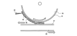
また図7に示すように、検査と、貼り合わせ加工を一連作業として行うことができる。第2の基板33をローラ85に設置し、白抜矢印方向に回転させる。このとき配線66が露出しているため、プローブ針80を用いて、チップ90の検査を行うことができる。検査終了後、良品と判断されたチップは、分断される。具体的には、ベルトコンベア86の表面に接着面を備える手段87を設けておき、白抜矢印方向に移動させ、第2の基板33からチップを剥離する。接着面を備える手段87としては、シリコーンゴム、パーフロロエラストマー、フルオンアフラス、テフロン(登録商標)(ポリテトラフルオロエチレンとも記す)ゴム等を使用することができる。特に、パーフロロエラストマー、フルオンアフラスは、耐熱性、耐薬品性の高く好ましい。このとき、接着面を備える手段87の接着強度は、第2の基板33が張り合わされている接着強度より高くなるように設定する。
Further, as shown in FIG. 7, the inspection and the bonding process can be performed as a series of operations. The
剥離層30が形成されない領域で、被剥離層69と第1の基板10とが一体化されている場合、ローラ85に設置したのち、第1の基板10を剥がすとよい。このとき、簡便に剥がせるように、剥離層30が形成されない領域の大きさを制御する。また、第2の基板33に形成する穴34を円状や矩形状とすることにより、被剥離層69と第2の基板33とが一体化されており、ばらばらになることを防止できる。このように被剥離層69がばらばらにならず、このように一体化されていることにより、ローラ85への設置が簡便になる。
When the layer to be peeled 69 and the
その後、チップ90は、ベルトコンベア86に乗せられ、貼り合わせ加工を施すことができる。
Thereafter, the
このように、チップの検査、貼り合わせ加工を一連作業で行うことにより、生産性を高めることができる。また接触式の検査は、非接触式と比べて、精度が高く、検査装置も簡便なものであるため好ましい。 In this manner, productivity can be improved by performing chip inspection and bonding processing in a series of operations. Further, the contact type inspection is preferable because the accuracy is high and the inspection apparatus is simpler than the non-contact type inspection.
また、剥離された第1の基板10、第2の基板33は再利用することができる。その結果、チップの低コスト化を達成することができる。再利用する場合、溝32を形成するためのダイシングやスクライビング等において、第1の基板10に傷が生成されないように制御するのが望ましい。しかし、傷が生成された場合であっても、塗布法や液滴吐出法によって有機樹脂や無機膜を形成し、平坦化処理を行なうことができる。なお液滴吐出法とは、導電膜や絶縁膜などの材料が混入された組成物の液滴(ドットとも表記する)を選択的に吐出(噴出)する方法であり、その方式によっては、インクジェット法とも呼ばれる。
Further, the peeled
また第2の基板33を用いずに、チップを形成する場合を説明する。図8(A)に示すように、絶縁膜70を形成した後、溝32を形成し、エッチング剤35を導入する。そして剥離層30を後退させて、第1の基板10を剥離する。なお絶縁膜70の具体的な材料として、エポキシ樹脂、アクリル樹脂、フェノール樹脂、ノボラック樹脂、メラミン樹脂、ウレタン樹脂、シリコン樹脂等の樹脂材料を用いることができる。また、ベンゾシクロブテン、パリレン、フレア、ポリイミドなどの有機材料、シロキサン系ポリマー等の重合によってできた化合物材料、水溶性ホモポリマーと水溶性共重合体を含む組成物材料が挙げられる。
A case where a chip is formed without using the
そして第1の基板10を剥離すると、図8(B)に示すように配線66が露出する。そこで、プローブ針80を用いて、接触式の検査を行うことができる。
Then, when the
その後、図8(C)に示すように、貼り合わせ加工を施し、両面を樹脂フィルム81で覆い、チップを完成させる。
Thereafter, as shown in FIG. 8C, bonding is performed, and both surfaces are covered with a
このように、第2の基板33を用いずにチップを形成すると、溝32と、穴34との位置あわせの制約がなく好ましい。
Thus, it is preferable to form a chip without using the
さらに第2の基板33を用いずに第1の基板を剥離する場合、ローラに絶縁膜70を粘着させ、ローラの回転力を用いて第1の基板を剥離することができる。
Further, when the first substrate is peeled off without using the
また第2の基板33を用いない場合であっても、溝32の形状によって、絶縁膜70により被剥離層69全体が一体化されている。そのため、図7に示すような、検査と、貼り合わせ加工を一連作業として行うことができる。
Even when the
このように完成されたチップにおいて、貼り合わせ加工を施す前に、その側面の周囲に、エポキシ樹脂等の有機樹脂を充填してもよい。その結果、チップは、貼り合わせ加工前であっても、外部から保護され、持ち運びしやすい形態となる。 In the chip thus completed, an organic resin such as an epoxy resin may be filled around the side surface before bonding. As a result, the chip is protected from the outside and easy to carry even before the bonding process.
このような無線チップは、アンテナを一体形成する場合に限定されず、アンテナを外付けして実装してもよい。この場合、配線66又は導電膜68と接続するようにバンプを設け、外付けするアンテナをバンプに接続すればよい。またさらに、露出された配線を介して、アンテナを外付けしてもよい。
Such a wireless chip is not limited to the case where the antenna is integrally formed, and may be mounted with the antenna attached externally. In this case, a bump may be provided so as to be connected to the
本発明のチップは、第3の基板72、つまりフレキシブル基板上に形成されている。また0.2μm以下、代表的には40nm〜170nm、好ましくは50nm〜150nmの膜厚の半導体膜を能動領域として有する。そのため、軽量化、薄型化を高めることができる。その結果、実装させる商品のデザイン性を損ねることがない。またフレキシブル性に富むため、チップの耐衝撃性を高めることができる。また曲面や異形形状な商品にチップを実装することができる。
The chip of the present invention is formed on a
なお本実施の形態において、第3の基板72を転置体とした場合を示したが、これに限定されない。例えば、第3の基板の代わりに、直接商品へ転置することも可能である。例えば、ラベル紙やタグ台紙に直接転置し、チップが実装された商品ラベルやタグを作製することができることは、上記実施の形態1と同様である。
Note that although the case where the
このような剥離方法を用いることより、大型基板に多数チップを形成する場合であっても、全面に剥離でき、歩留まりよく、チップを形成することができる。 By using such a peeling method, even when a large number of chips are formed on a large substrate, the entire surface can be peeled off, and a chip can be formed with a high yield.
なお本発明は、チップ完成前に、接触式の検査を行うことができればよく、チップの作製方法、特に剥離方法には限定されない。但し本実施の形態のような剥離方法を用いることにより、TFT完成後にレーザー照射することがないため、TFT等に負荷をかけることがなく好ましい。また本実施の形態のような剥離方法では、第1の基板10、第2の基板等を再利用することができるため好ましい。その結果、更に安価なフィルム基板を使用するためコストを抑えたチップを提供することができる。
Note that the present invention is not limited to a chip manufacturing method, particularly a peeling method, as long as a contact type inspection can be performed before the chip is completed. However, it is preferable to use a peeling method as in this embodiment mode, because laser irradiation is not performed after the TFT is completed, so that no load is applied to the TFT or the like. Further, the peeling method as in this embodiment is preferable because the
さらにこのような矩形上の基板からチップを形成する場合、円形のシリコンウェハからチップを取り出す場合と比較して、母体基板形状に制約がない。そのため、チップの生産性を高め、大量生産を行うことができる。 Further, when the chip is formed from such a rectangular substrate, the shape of the base substrate is not limited as compared with the case where the chip is taken out from the circular silicon wafer. Therefore, the productivity of chips can be increased and mass production can be performed.
例えば、直径12インチのシリコンウェハを用いた場合と、730×920mm2のガラス基板を用いた場合とで取り数等を比較する。前者のシリコン基板の面積は約73000mm2であるが、後者のガラス基板の面積は約672000mm2であり、ガラス基板はシリコン基板の約9.2倍に相当する。後者のガラス基板の面積は約672000mm2では、基板の分断により消費される面積を無視すると、1mm四方のチップが約672000個形成できる計算になり、該個数はシリコン基板の約9.2倍の数に相当する。そしてチップの量産化を行なうための設備投資は、730×920mm2のガラス基板を用いた場合の方が直径12インチのシリコン基板を用いた場合よりも工程数が少なくて済むため、額を3分の1で済ませることができる。 For example, the number of picks and the like are compared between a case where a silicon wafer having a diameter of 12 inches is used and a case where a glass substrate of 730 × 920 mm 2 is used. The area of the former silicon substrate is about 73000 mm 2 , while the area of the latter glass substrate is about 672000 mm 2 , and the glass substrate corresponds to about 9.2 times the silicon substrate. When the area of the latter glass substrate is about 672000 mm 2 , ignoring the area consumed by dividing the substrate, it is calculated that about 672,000 chips of 1 mm square can be formed, and the number is about 9.2 times that of the silicon substrate. It corresponds to a number. The capital investment for mass production of chips requires 3 steps because the number of processes is smaller when a glass substrate of 730 × 920 mm 2 is used than when a silicon substrate of 12 inches in diameter is used. You can do it in a minute.
その結果、チップのコストを削減できる。単価が非常に低いチップは、単価コストの削減により非常に大きな利益を生むことができる。 As a result, the cost of the chip can be reduced. A chip with a very low unit price can make a huge profit by reducing the unit cost.
また本発明のチップは、シリコンウェハから形成されるチップと比較して、電波吸収の心配がなく、高感度な信号の受信を行なうことができる。 Further, the chip of the present invention can receive a highly sensitive signal without worrying about radio wave absorption as compared with a chip formed from a silicon wafer.
さらに本発明のチップは、シリコンウェハを有さないため、透光性を有することができる。その結果、実装品の印字面に実装しても、デザイン性を損ねることがない。 Furthermore, since the chip of the present invention does not have a silicon wafer, it can have translucency. As a result, even if it is mounted on the printed surface of the mounted product, the design is not impaired.
本発明の無線チップは、アンテナにより電力、又は信号を得ることができる。
アンテナが実装されている本発明の無線チップは、非接触型チップと呼ぶことができる。なお、アンテナは実装せずに、接続端子を形成した接触型チップ、非接触型及び接触型とが混在したハイブリッド型チップがあるが、本実施の形態で示した接触式の検査方法は、非接触型チップ以外の、接触型チップ、及びハイブリッド型チップのいずれにも適用することができる。
The wireless chip of the present invention can obtain power or a signal with an antenna.
The wireless chip of the present invention on which an antenna is mounted can be called a non-contact type chip. Note that there is a contact type chip in which a connection terminal is formed without mounting an antenna, and a hybrid type chip in which a non-contact type and a contact type are mixed. However, the contact type inspection method described in this embodiment is not The present invention can be applied to any of a contact chip and a hybrid chip other than the contact chip.
(実施の形態3)
本実施の形態では、上記実施の形態を組み合わせた方法により、チップを作製する工程について説明する。
(Embodiment 3)
In this embodiment, a process for manufacturing a chip by a method in which the above embodiments are combined will be described.
例えば、剥離層30に金属膜、及び珪素を有する膜を積層して用いることができる。その結果、両者の剥離条件のいずれかを満たせばよいこととなり、プロセスマージンを広げることができる。
For example, the
また、剥離層30に金属膜を用い、ダイシング等により溝32を形成する。そして、溝に金属膜のみをエッチングするエッチング剤を導入して、第1の基板10を剥離することができる。
Further, a metal film is used for the
このように、実施の形態1と実施の形態2とは自由に組み合わせることができる。
Thus,
(実施の形態4)
本実施の形態では、上記実施の形態で示した薄膜トランジスタと異なる構成の薄膜トランジスタについて詳述する。
(Embodiment 4)
In this embodiment, a thin film transistor having a structure different from that of the thin film transistor described in the above embodiment is described in detail.
薄膜トランジスタの構成は、上記実施の形態で示したように半導体膜上にゲート電極62、64が設けられたトップゲート型以外に、半導体膜を挟んで上下にゲート電極(上部ゲート電極、及び下部ゲート電極と表記する)が設けられたデュアルゲート型を用いることができる。本実施の形態では、接着剤73を介して第3の基板72に貼り付けられたデュアルゲート型の薄膜トランジスタの構成を、図9を用いて説明する。
The structure of the thin film transistor is not limited to the top gate type in which the
まず、下部ゲート電極91として機能する導電膜を形成する。導電膜は、金属又は一導電型の不純物を添加した多結晶半導体で形成することができる。金属を用いる場合は、タングステン(W)、モリブデン(Mo)、チタン(Ti)、タンタル(Ta)、アルミニウム(Al)などを用いることができる。下部ゲート電極91は、マスク、例えばレジストマスクを用いて、所定の形状にエッチングする。このとき、微細な下部ゲート電極を形成するため、酸素プラズマにより細められたレジストマスクを用いてエッチングしてもよい。
First, a conductive film functioning as the
そして、下地膜として機能する絶縁膜を形成する。本実施の形態では、窒素を有する酸化珪素膜(SiON)55、酸素を有する窒化珪素膜(SiNO)56、窒素を有する酸化珪素膜(SiON)57を順に積層するが、これに限定されない。例えば、酸素を有する窒化珪素膜(SiNO)からなる単層構造を用いてもよい。下地膜により、第3の基板72や接着剤73からの不純物、下部ゲート電極91からの金属の、半導体膜への拡散を防止することができる。
Then, an insulating film functioning as a base film is formed. In this embodiment mode, a silicon oxide film (SiON) 55 containing nitrogen, a silicon nitride film (SiNO) 56 containing oxygen, and a silicon oxide film (SiON) 57 containing nitrogen are sequentially stacked. However, the present invention is not limited to this. For example, a single layer structure made of a silicon nitride film containing oxygen (SiNO) may be used. The base film can prevent the impurities from the
次に、所定の形状を有する半導体膜、半導体膜を覆って設けられたゲート絶縁膜58、上部ゲート電極62、64として機能する導電膜を順に設ける。これらの材料や作製方法は、上記実施の形態を参照することができる。
Next, a semiconductor film having a predetermined shape, a
なお、上部ゲート電極62、64を所定の形状にパターニングするためのレジストマスクを形成する。このとき、下部ゲート電極91を用いた裏面露光により所定の形状を有するレジストマスクを形成することができる。そして、当該レジストマスクを用いて、パターニングすることができる。このように、下部ゲート電極を用いてレジストマスクを露光することにより、上部ゲート電極の位置合わせの制約を緩和することができる。
A resist mask for patterning the
なお、上記実施の形態に示したように、上部ゲート電極62、64を積層構造とする場合、上部ゲート電極の下層電極をパターニングするときに、下部ゲート電極91を用いて露光されたレジストマスクを用いる。その後、上層電極を形成する。
As shown in the above embodiment, when the
その後、上部ゲート電極62、64を用いて、半導体膜に不純物元素を添加する。このとき、上記実施の形態のようにサイドウォールとして機能する絶縁物を設け、低濃度不純物領域の大きさ等を制御することができる。
Thereafter, an impurity element is added to the semiconductor film using the
また上部ゲート電極62、64を積層構造とする場合、上層電極を用いて、低濃度不純物領域を形成することができる。このとき、低濃度不純物領域は、下層電極と重なるため、GOLD構造となる。
Further, when the
そして、下部ゲート電極91と、上部ゲート電極62、64を別に制御するため、それぞれに配線を接続する。まず、下部ゲート電極91に接続される配線を設けるため、上部ゲート電極62、64の一部を除去してコンタクトホールを形成する。上部ゲート電極62、64が下層電極と、上層電極との積層構造の場合、下層電極の一部を除去する。
Then, in order to separately control the
なお下部ゲート電極91と、上部ゲート電極62、64とを同じように制御する場合、上記のように上部ゲート電極62、64の一部を除去する必要はない。下部ゲート電極91上に設けられるゲート絶縁膜58にコンタクトホールを形成し、当該コンタクトホールに直接上部ゲート電極62、64を形成すればよい。
When the
その後、ゲート電極を覆って、絶縁膜59、67を形成する。絶縁膜59、67は、無機材料、又は有機材料から形成することができる。また上記実施の形態に示すように絶縁膜59以外の絶縁膜を積層してもよい。また絶縁膜67によって、平坦性を高める場合、絶縁膜67は有機材料を用いると好ましい。
Thereafter, insulating
その後、絶縁膜59、67、ゲート絶縁膜47に開口領域を形成し、不純物領域と接続する配線66として機能する導電膜を形成する。その後、配線66を覆って絶縁膜93を設けることができる。絶縁膜93は、無機材料又は有機材料から形成することができる。また積層構造であっても、単層構造であってもよい。
Thereafter, an opening region is formed in the insulating
このとき、開口領域の一部は、下部ゲート電極91と同一層までエッチングする。そのため、第1の基板10を剥離後、配線66が露出し、接触式の検査を行うことができる。
At this time, a part of the opening region is etched to the same layer as the
配線66に、さらに接続される導電膜68を形成してもよい。アンテナは、配線66、又は導電膜68を用いて、形成することができる。
A
このようにして下部ゲート電極91を有するデュアルゲート型の薄膜トランジスタを、チップの論理回路に適用することができる。下部ゲート電極91は、上部ゲート電極62、64と別に制御することができる。そのため、ゲート電極が微細な薄膜トランジスタを形成する場合、上部ゲート電極にオフとなる信号を入力するときに電流が流れてしまうことがあっても、下部ゲート電極91を制御することにより、正確にオフ状態とすることができる。その結果、低消費電力化を図ることができる。
In this manner, the dual gate type thin film transistor having the
具体的には、N型の薄膜トランジスタ36をデュアルゲート型とする場合、下部ゲート電極91に対する負のバイアス電圧の印加は、しきい値電圧を高めることによって、リーク電流を減少させることができる。また、正のバイアス電圧の印加は、しきい値電圧を下げることによって、チャネル形成領域に電流が流れやすくすることができる。従って、デュアルゲート型の薄膜トランジスタは、より高速化、若しくはより低電圧で動作することができる。
Specifically, when the N-type
本実施の形態は、上記の実施の形態と自由に組み合わせることができる。 This embodiment mode can be freely combined with the above embodiment modes.
(実施の形態5)
本実施の形態では、上記実施の形態と異なるTFTの構成について説明する。
(Embodiment 5)
In this embodiment, a structure of a TFT which is different from that in the above embodiment is described.
図10は、半導体膜下方にゲート電極を有するボトムゲート型の薄膜トランジスタを示す。なお本実施の形態において、接着剤73を介して第3の基板72に貼り付けられた状態のボトムゲート型の薄膜トランジスタを説明する。
FIG. 10 shows a bottom-gate thin film transistor having a gate electrode below a semiconductor film. Note that in this embodiment, a bottom-gate thin film transistor which is attached to the
接着剤73を介して第3の基板72に貼り付けられたボトムゲート型薄膜トランジスタは、下地膜上にゲート電極304として機能する導電膜が設けられている。本実施の形態では、下地膜として、窒素を有する酸化珪素膜(SiON)55、酸素を有する窒化珪素膜(SiNO)56、窒素を有する酸化珪素膜(SiON)57を順に積層するが、これに限定されない。例えば、酸素を有する窒化珪素膜(SiNO)からなる単層構造を用いてもよい。
In the bottom gate thin film transistor attached to the
ゲート電極304は、単層構造であっても、積層構造であってもよく、Ta、W、Ti、Mo、Al、Cuから選ばれた元素、または前記元素を主成分とする合金材料もしくは化合物材料で形成することができる。なお、その後の工程において加熱処理を施す場合、Wのように、耐熱性の高い材料を用いるとよい。さらには耐熱性を高めるため陽極酸化法を用いて、ゲート電極304の周りに絶縁物を形成してもよい。
The
その後、ゲート絶縁膜58として機能する絶縁膜、半導体膜を形成する。半導体膜は、非晶質半導体、SASを用いると好ましいが、結晶性半導体膜を用いてもよい。例えば非晶質半導体膜を形成後、加熱処理を施し結晶性半導体膜を形成することができる。このとき、ゲート電極の耐熱性を考慮する必要がある。
Thereafter, an insulating film and a semiconductor film functioning as the
その後半導体膜上に、チャネル保護膜309として機能する絶縁膜を形成する。チャネル保護膜309により、半導体膜がエッチングされることを防止することができ好ましいが、必ずしもチャネル保護膜309は必要ではない。
After that, an insulating film functioning as a channel
その後、これらを覆って絶縁膜305を形成する。絶縁膜305は無機材料、又は有機材料から形成することができる。本実施の形態では、半導体膜への不純物等汚染を防止することを考え、窒素を有する酸化珪素膜(SiON)を用いて絶縁膜305を形成する。
Thereafter, an insulating
そして、半導体膜に接続する配線66を形成するため、開口領域を形成する。本実施の形態では、一方の配線66のみを形成する。このとき、開口領域の一部は、下地膜までエッチングする。そのため、第1の基板10を剥離後、配線66が露出し、接触式の検査を行うことができる。
Then, an opening region is formed in order to form the
またコンタクト抵抗を下げるため、n型を有する半導体膜を、配線66と、半導体膜との接続箇所に設けてもよい。
In order to reduce contact resistance, an n-type semiconductor film may be provided at a connection portion between the
その後、絶縁膜67を設ける。絶縁膜67は、無機材料、又は有機材料から形成することができる。平坦性を高めるためには有機材料を用いるとよい。
Thereafter, an insulating
そして他方の配線66を形成するため、絶縁膜67、305に開口領域を形成する。このとき、開口領域の一部を、下地膜までエッチングすることができる。その結果、第1の基板10を剥離後、配線66が露出し、接触式の検査を行うことができる。
Then, an opening region is formed in the insulating
その後、配線66、絶縁膜67を覆うように、絶縁膜93を形成する。絶縁膜93は、無機材料、又は有機材料から形成することができるが、不純物等の汚染を防止することを考え、窒素を有する酸化珪素膜(SiON)を用いて絶縁膜93を形成する。
Thereafter, an insulating
このような構造を有するボトムゲート型薄膜トランジスタを、チップの論理回路に適用することができる。 A bottom-gate thin film transistor having such a structure can be applied to a logic circuit of a chip.
なお、チップの論理回路に用いられる薄膜トランジスタは、上記実施の形態のようなトップゲート型、デュアルゲート型であっても、ボトムゲート型であってもよい。またトップゲート型と、ボトムゲート型、デュアルゲート型をそれぞれ組み合わせて用いてもよい。 Note that the thin film transistor used for the logic circuit of the chip may be a top gate type, a dual gate type as in the above embodiment, or a bottom gate type. Further, a top gate type, a bottom gate type, and a dual gate type may be used in combination.
本実施の形態は、上記の実施の形態と自由に組み合わせることができる。 This embodiment mode can be freely combined with the above embodiment modes.
(実施の形態6)
本実施の形態では、多層配線構造について説明する。
(Embodiment 6)
In this embodiment, a multilayer wiring structure will be described.
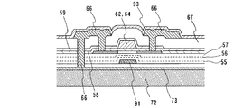
チップのように小さな面積に、論理回路を形成する場合、回路同士、薄膜トランジスタ同士を接続する配線を多層構造とすると集積化でき、好ましい。本実施の形態では、トップゲート型の薄膜トランジスタを用いて、多層配線構造について説明する。 In the case of forming a logic circuit in a small area like a chip, it is preferable that the wiring connecting the circuits and the thin film transistors has a multi-layer structure, which can be integrated. In this embodiment mode, a multilayer wiring structure is described using top-gate thin film transistors.
図11には、配線66と接続される配線42、配線42に接続される配線45が積層される薄膜トランジスタを示す。配線66、42、45の材料は、上記実施の形態と同様に、アルミニウム(Al)、チタン(Ti)、モリブデン(Mo)、タングステン(W)もしくはシリコン(Si)の元素からなる膜又はこれらの元素を用いた合金膜を用いればよい。
FIG. 11 illustrates a thin film transistor in which a
このとき、配線間に設けられる絶縁膜は、無機材料、又は有機材料から形成することができ、絶縁膜単層構造であっても、積層構造であってもよいが、好ましくは無機材料と、有機材料の積層構造とするとよい。本実施の形態では、配線66、配線42間に設けられる絶縁膜40に、窒素を有する酸化珪素膜(SiON)を用い、絶縁膜41にシロキサンを用いることができる。これら無機材料により、不純物等の汚染防止をはかり、有機材料により平坦性を高めることができる。同様に、配線42、配線45間に設けられる絶縁膜43に、窒素を有する酸化珪素膜(SiON)を用い、絶縁膜44にシロキサンを用いることができる。
At this time, the insulating film provided between the wirings can be formed from an inorganic material or an organic material, and may have a single-layer structure or a laminated structure, but preferably an inorganic material, A stacked structure of organic materials is preferable. In this embodiment mode, a silicon oxide film (SiON) containing nitrogen can be used for the insulating
このような積層構造を有する絶縁膜の構成は、多層配線構造に好適である。 The structure of the insulating film having such a laminated structure is suitable for a multilayer wiring structure.
本実施の形態は、上記実施の形態と自由に組み合わせることができる。 This embodiment can be freely combined with the above embodiment.
(実施の形態7)
本実施の形態では、積層された薄膜トランジスタ構造について説明する。
(Embodiment 7)
In this embodiment mode, a stacked thin film transistor structure is described.
第1の基板10を剥離後、配線66が露出するため、これらを積層することが簡便となる。例えば、図12には、薄膜トランジスタ36、37を3つ積層した構造を示す。各層の薄膜トランジスタを36(1)、36(2)、36(3)、及び37(1)、37(2)、37(3)とし、それぞれの配線を66(1)、66(2)、66(3)とする。
Since the
接触式の検査を得て、論理回路に分断された薄膜トランジスタは、配線66を介して積層される。このとき、配線66が露出しているため、接続するためのバンプ、ワイヤボンディングを不要とすることができる。
The thin film transistors obtained by the contact type inspection and divided into logic circuits are stacked through the
そのため、上部の薄膜トランジスタに向けて、論理回路領域を小さくする必要がなく、高集積化を達成することができる。 Therefore, it is not necessary to reduce the logic circuit area toward the upper thin film transistor, and high integration can be achieved.
また第3の層には、配線66(3)と接続される導電膜68を形成する。導電膜68はアンテナとして機能することができる。なお導電膜68は第3の層に形成することに限定されず、第1の層、第2の層に形成してもよい。
In the third layer, a
このように配線66を露出することにより、積層された薄膜トランジスタを簡便に作製することができる。
By exposing the
このような積層された薄膜トランジスタ構造は、各層にセンサー機能を持たせ、複合センサー装置に適用できる。例えば、第1層目の薄膜トランジスタを用いて圧力センサーを形成し、第2層目の薄膜トランジスタを用いて温度センサーを形成し、第3層目の薄膜トランジスタを用いてフォトセンサーを形成することができる。 Such a stacked thin film transistor structure can be applied to a composite sensor device by providing each layer with a sensor function. For example, a pressure sensor can be formed using a first thin film transistor, a temperature sensor can be formed using a second thin film transistor, and a photosensor can be formed using a third thin film transistor.
特に多層配線構造で示したように、配線66に接して形成される絶縁膜には、無機材料と有機材料とが積層した構造を用いるとよい。
In particular, as shown in the multilayer wiring structure, the insulating film formed in contact with the
またさらに、露出された配線を介して、アンテナを貼り付けてもよい。 Furthermore, an antenna may be attached via the exposed wiring.
本実施の形態は、上記実施の形態と自由に組み合わせることができる。 This embodiment can be freely combined with the above embodiment.
(実施の形態8)
本実施の形態では、貼り合わせ加工された無線チップの断面図について説明する。
(Embodiment 8)
In this embodiment, a cross-sectional view of a bonded wireless chip is described.
無線チップは、アンテナより電源を供給するため、電源の安定化が難しく、消費電力を極力抑制することが必要である。仮に、消費電力が増加すると、電磁波を入力する必要があるため、リーダライタの消費電力の増加、他の装置や人体への悪影響、無線チップとリーダライタとの通信距離に制約が生じるなどの不都合が生じる。 Since a wireless chip supplies power from an antenna, it is difficult to stabilize the power supply, and it is necessary to suppress power consumption as much as possible. If the power consumption increases, it is necessary to input electromagnetic waves, which increases the power consumption of the reader / writer, adverse effects on other devices and the human body, and restrictions on the communication distance between the wireless chip and the reader / writer. Occurs.
そこで、本実施の形態では、消費電力を抑制することが可能とするため、デュアルゲート構造の薄膜トランジスタを用いて無線チップを形成することを特徴とする。 Therefore, in this embodiment, in order to reduce power consumption, a wireless chip is formed using a dual-gate thin film transistor.
図13には、下部ゲート電極91と上部ゲート電極62を含むN型の薄膜トランジスタ36と、下部ゲート電極91と上部ゲート電極64を含むP型の薄膜トランジスタ37を示す。
FIG. 13 shows an N-type
また無線チップに対して貼り合わせ加工を行って、論理回路等を構成する薄膜トランジスタを、第1の基体53と第2の基体54により封止する。このようにして、第1の基体53と第2の基体54により封止された無線チップが完成する。
Further, bonding processing is performed on the wireless chip, and the thin film transistors forming the logic circuit and the like are sealed with the
上記の通り、下部ゲート電極91に印加するバイアス電圧を制御することで、薄膜トランジスタ36、37のしきい値電圧を変えて、リーク電流を減少させ、その結果、無線チップ自体の消費電力を抑制することができる。従って、暗号処理などの複雑な処理を行っても、電源が不安定になることがなく、電源の安定化を実現する。また、電磁波を入力する必要がなく、リーダライタとの通信距離を改善することができる。なお、バイアス電圧の印加は、専用の制御回路を設けて、アンテナを介した電源の状態によって切り換えるとよい。
As described above, by controlling the bias voltage applied to the
なおデュアルゲート構造の薄膜トランジスタを用いる場合を説明したが、図14に示すように、シングルゲート構造の薄膜トランジスタを用いてもよい。図14には、シングルゲート構造のN型の薄膜トランジスタ36、及びP型の薄膜トランジスタ37を示す。
Note that although the case of using a dual-gate thin film transistor has been described, a single-gate thin film transistor may be used as shown in FIG. FIG. 14 shows a single-gate N-type
なお図14において、薄膜トランジスタ、アンテナ、及び保護層までの厚みは、20μm〜40μmであり、第1の基体53及び第2の基体54のそれぞれの膜厚は、15μm〜35μmである。
In FIG. 14, the thickness up to the thin film transistor, antenna, and protective layer is 20 μm to 40 μm, and the thickness of each of the
本実施の形態は、上記の実施の形態と自由に組み合わせることができる。 This embodiment mode can be freely combined with the above embodiment modes.
なお接触型チップの場合、図13、図14において、アンテナを形成しない構成とすればよい。但し、接触型チップは、接続端子を露出しておくため、貼り合わせ加工のとき、その領域を開口しておく。 Note that in the case of a contact-type chip, a structure in which an antenna is not formed in FIGS. However, since the contact-type chip exposes the connection terminals, the area is opened during the bonding process.
(実施の形態9)
本発明のチップの用途は広範にわたり、あらゆる商品に実装することができる。例えば、紙幣、硬貨、有価証券類、無記名債券類、証書類(運転免許証や住民票等、図15(A)参照)、包装用容器類(包装紙やボトル等、図15(B)参照)、記録媒体(DVDソフトやビデオテープ等、図15(C)参照)、乗物類(自転車等、図15(D)参照)、装身具(鞄や眼鏡等、図15(E)参照)、食品類、衣類、生活用品類、電子機器等に貼り付けて使用することができる。電子機器とは、液晶表示装置、EL表示装置、テレビジョン装置(単にテレビ、テレビ受像機、テレビジョン受像機とも呼ぶ)、コンピュータ、及び携帯電話機等を指す。このように電子機器に貼り付ける場合、チップにより電子機器の機能を補助することができる。特にコンピュータや携帯電話機にチップを貼り付ける場合、メモリ機能の補助をすることができる。このようなチップであって、無線通信を行うものを無線メモリと呼ぶ。またこのようなチップは、コンピュータや携帯電話機に差し込んで使用するため、接続端子を有する接触型であってもよい。
(Embodiment 9)
The application of the chip of the present invention is wide-ranging and can be mounted on any product. For example, banknotes, coins, securities, bearer bonds, certificates (driver's license, resident card, etc., see FIG. 15A), packaging containers (wrapping paper, bottles, etc., see FIG. 15B) ), Recording media (DVD software, videotape, etc., see FIG. 15C), vehicles (bicycles, etc., see FIG. 15D), accessories (such as bags and glasses, see FIG. 15E), food It can be used by sticking it to clothing, clothing, daily necessities, electronic devices and the like. Electronic devices refer to liquid crystal display devices, EL display devices, television devices (also simply referred to as televisions, television receivers, television receivers), computers, mobile phones, and the like. Thus, when pasting on an electronic device, the function of the electronic device can be assisted by the chip. In particular, when a chip is attached to a computer or mobile phone, the memory function can be assisted. Such a chip that performs wireless communication is called a wireless memory. Further, since such a chip is used by being inserted into a computer or a mobile phone, it may be a contact type having a connection terminal.
チップは、商品の表面に貼ったり、商品に埋め込んだりして、商品に固定することができる。例えば、本なら表紙の厚紙に埋め込んだり、有機樹脂からなるパッケージなら当該有機樹脂に埋め込んだりする。また、紙幣、硬貨、有価証券類、無記名債券類、証書類等なら、表面に貼り付けたり、埋め込んだりする。上記に挙げた商品のうち、例えば、包装用容器類、記録媒体、身の回り品、食品類、衣類、生活用品類、電子機器等にチップを設けることにより、検品システムやレンタル店のシステムなどの効率化を図ることができる。このように商品に埋め込む場合、無線通信を行う無線チップを用いると好ましい。 The chip can be fixed to the product by being affixed to the surface of the product or embedded in the product. For example, a book is embedded in a cardboard of a cover, and a package made of an organic resin is embedded in the organic resin. For banknotes, coins, securities, bearer bonds, certificates, etc., they are pasted or embedded on the surface. Among the products listed above, for example, by providing chips on packaging containers, recording media, personal items, foods, clothing, daily necessities, electronic devices, etc., the efficiency of inspection systems, rental store systems, etc. Can be achieved. When embedding in a product as described above, it is preferable to use a wireless chip that performs wireless communication.
また、チップを、物の管理や流通のシステムに応用することで、システムの高機能化を図ることができる。例えば、表示部294を含む携帯端末の側面にリーダライタ295を設けて、商品297の側面にチップ296を設ける場合が挙げられる(図16(A)参照)。この場合、リーダライタ295にチップ296をかざすと、表示部294に商品297の原材料や原産地、流通過程の履歴等の情報が表示されるシステムになっている。また、別の例として、ベルトコンベアの脇にリーダライタ295を設ける場合が挙げられる(図16(B)参照)。この場合、商品297には、チップが実装されたラベルが貼られており、の検品を簡単に行うことができる。このようにリーダライタにかざす場合、無線通信を行う無線チップを使用する。
In addition, by applying the chip to a system for managing and distributing goods, it is possible to improve the functionality of the system. For example, the reader /
またさらに、チップは動物の管理にも使用することができる。例えば、家畜等にチップを埋め込み、健康状態等を管理することができる。またペットの首輪等にチップを貼り付け、迷子のときの現在地を把握することもできる。このような動物管理に用いる場合、無線通信を行う無線チップを使用する。 Furthermore, the chip can also be used for animal management. For example, it is possible to embed a chip in livestock or the like to manage the health condition. You can also attach a tip to your pet's collar to find out where you are when you are lost. When used for such animal management, a wireless chip that performs wireless communication is used.
また医療にチップを用いることができる。このようなチップは、無線通信を行う無線チップを用いると好ましい。医療に用いる無線チップを医療用無線チップと呼ぶ。 A chip can be used for medical treatment. Such a chip is preferably a wireless chip that performs wireless communication. A wireless chip used for medical treatment is called a medical wireless chip.
また接触型チップは、カードに搭載することができる。また、集積回路(LSI)の機能を補助するため、端子を介して接触型チップを実装してもよい。 The contact chip can be mounted on a card. Further, in order to assist the function of the integrated circuit (LSI), a contact type chip may be mounted through a terminal.
本実施の形態は、上記の実施の形態と自由に組み合わせることができる。 This embodiment mode can be freely combined with the above embodiment modes.
Claims (4)
前記剥離層上に第1の絶縁膜を形成し、Forming a first insulating film on the release layer;
前記第1の絶縁膜上にp型の不純物領域の半導体層を有する第1の薄膜トランジスタとn型の不純物領域の半導体層を有する第2の薄膜トランジスタとを形成し、Forming a first thin film transistor having a semiconductor layer of a p-type impurity region and a second thin film transistor having a semiconductor layer of an n-type impurity region on the first insulating film;
前記第1の薄膜トランジスタと前記第2の薄膜トランジスタとの上に第2の絶縁膜を形成し、Forming a second insulating film on the first thin film transistor and the second thin film transistor;
前記第1の絶縁膜と前記第2の絶縁膜との一部を開口し第1の開口領域を形成し、Forming a first opening region by opening a part of the first insulating film and the second insulating film;
前記第1の開口領域に、前記剥離層に接するように、前記第1の薄膜トランジスタの半導体層の不純物領域と前記第2の薄膜トランジスタの半導体層の不純物領域とに電気的に接続される導電膜を形成し、A conductive film electrically connected to the impurity region of the semiconductor layer of the first thin film transistor and the impurity region of the semiconductor layer of the second thin film transistor so as to be in contact with the peeling layer in the first opening region Forming,
前記導電膜上に第3の絶縁膜を形成し、Forming a third insulating film on the conductive film;
前記第1の絶縁膜と前記第2の絶縁膜と前記第3の絶縁膜との一部を開口し第2の開口領域を形成し、Opening a part of the first insulating film, the second insulating film, and the third insulating film to form a second opening region;
前記第3の絶縁膜上に前記第2の開口領域に合わせて複数の穴が設けられた第2の基板を貼り合わせ、A second substrate provided with a plurality of holes in accordance with the second opening region is bonded to the third insulating film,
前記複数の穴を介して、前記第2の開口領域にエッチング剤を導入し、前記剥離層をエッチングし前記第1の基板を剥離することにより、前記導電膜を露出させ、Introducing an etchant into the second opening region through the plurality of holes, etching the release layer and peeling the first substrate, thereby exposing the conductive film,
前記第2の基板が接するようにローラ上に設置し、Installed on a roller so that the second substrate contacts,
前記ローラを回転させ、前記露出された導電膜にプローブ針を接触させて検査を行い、接着面を備えるベルトコンベアと前記第1の絶縁膜と前記導電膜とを接着し、前記第2の基板を剥離することを特徴とする半導体装置の作製方法。The second substrate is rotated by rotating the roller, bringing a probe needle into contact with the exposed conductive film, inspecting, bonding a belt conveyor having an adhesive surface, the first insulating film, and the conductive film. A method for manufacturing a semiconductor device, comprising: peeling off a semiconductor device.
前記剥離層上に第1の絶縁膜を形成し、Forming a first insulating film on the release layer;
前記第1の絶縁膜上にp型の不純物領域の半導体層を有する第1の薄膜トランジスタとn型の不純物領域の半導体層を有する第2の薄膜トランジスタとを形成し、Forming a first thin film transistor having a semiconductor layer of a p-type impurity region and a second thin film transistor having a semiconductor layer of an n-type impurity region on the first insulating film;
前記第1の薄膜トランジスタと前記第2の薄膜トランジスタとの上に第2の絶縁膜を形成し、Forming a second insulating film on the first thin film transistor and the second thin film transistor;
前記第1の絶縁膜と前記第2の絶縁膜との一部を開口し、Opening a part of the first insulating film and the second insulating film;
前記開口された領域に、前記剥離層に接するように、前記第1の薄膜トランジスタの半導体層の不純物領域と前記第2の薄膜トランジスタの半導体層の不純物領域とに電気的に接続される導電膜を形成し、A conductive film electrically connected to the impurity region of the semiconductor layer of the first thin film transistor and the impurity region of the semiconductor layer of the second thin film transistor is formed in the opened region so as to be in contact with the peeling layer. And
前記導電膜上に第3の絶縁膜を形成し、Forming a third insulating film on the conductive film;
前記第3の絶縁膜上に第2の基板を貼り合わせ、A second substrate is bonded onto the third insulating film,
前記剥離層に対して加熱処理を行い、物理的手段を用いて前記第1の基板を剥離することにより、前記導電膜を露出させ、Heat treatment is performed on the release layer, and the conductive substrate is exposed by peeling the first substrate using physical means,
前記第2の基板が接するようにローラ上に設置し、Installed on a roller so that the second substrate contacts,
前記ローラを回転させ、前記露出された導電膜にプローブ針を接触させて検査を行い、接着面を備えるベルトコンベアと前記第1の絶縁膜と前記導電膜とを接着し、前記第2の基板を剥離することを特徴とする半導体装置の作製方法。The second substrate is rotated by rotating the roller, bringing a probe needle into contact with the exposed conductive film, inspecting, bonding a belt conveyor having an adhesive surface, the first insulating film, and the conductive film. A method for manufacturing a semiconductor device, comprising: peeling off a semiconductor device.
前記剥離層上に第1の絶縁膜を形成し、Forming a first insulating film on the release layer;
前記第1の絶縁膜上にp型の不純物領域の半導体層を有する第1の薄膜トランジスタとn型の不純物領域の半導体層を有する第2の薄膜トランジスタとを形成し、Forming a first thin film transistor having a semiconductor layer of a p-type impurity region and a second thin film transistor having a semiconductor layer of an n-type impurity region on the first insulating film;
前記第1の薄膜トランジスタと前記第2の薄膜トランジスタとの上に第2の絶縁膜を形成し、Forming a second insulating film on the first thin film transistor and the second thin film transistor;
前記第1の絶縁膜と前記第2の絶縁膜との一部を開口し第1の開口領域を形成し、Forming a first opening region by opening a part of the first insulating film and the second insulating film;
前記第1の開口領域に、前記剥離層に接するように、前記第1の薄膜トランジスタの半導体層の不純物領域と前記第2の薄膜トランジスタの半導体層の不純物領域とに電気的に接続される導電膜を形成し、A conductive film electrically connected to the impurity region of the semiconductor layer of the first thin film transistor and the impurity region of the semiconductor layer of the second thin film transistor so as to be in contact with the peeling layer in the first opening region Forming,
前記導電膜上に第3の絶縁膜を形成し、Forming a third insulating film on the conductive film;
前記第3の絶縁膜の一部を開口し、コンタクトホールを形成し、Opening a part of the third insulating film to form a contact hole;
前記コンタクトホールを介して、前記第3の絶縁膜上に前記第1の薄膜トランジスタまたは前記第2のトランジスタと電気的に接続するアンテナを形成し、Forming an antenna electrically connected to the first thin film transistor or the second transistor over the third insulating film through the contact hole;
前記アンテナ上に第4の絶縁膜を形成し、Forming a fourth insulating film on the antenna;
前記第1の絶縁膜と前記第2の絶縁膜と前記第3の絶縁膜と前記第4の絶縁膜との一部を開口し第2の開口領域を形成し、Opening a part of the first insulating film, the second insulating film, the third insulating film, and the fourth insulating film to form a second opening region;
前記第3の絶縁膜上に前記第2の開口領域に合わせて複数の穴が設けられた第2の基板を貼り合わせ、A second substrate provided with a plurality of holes in accordance with the second opening region is bonded to the third insulating film,
前記複数の穴を介して、前記第2の開口領域にエッチング剤を導入し、前記剥離層をエッチングし前記第1の基板を剥離することにより、前記導電膜を露出させ、Introducing an etchant into the second opening region through the plurality of holes, etching the release layer and peeling the first substrate, thereby exposing the conductive film,
前記第2の基板が接するようにローラ上に設置し、Installed on a roller so that the second substrate contacts,
前記ローラを回転させ、前記露出された導電膜にプローブ針を接触させて検査を行い、接着面を備えるベルトコンベアと前記第1の絶縁膜と前記導電膜とを接着し、前記第2の基板を剥離することを特徴とする半導体装置の作製方法。The second substrate is rotated by rotating the roller, bringing a probe needle into contact with the exposed conductive film, inspecting, bonding a belt conveyor having an adhesive surface, the first insulating film, and the conductive film. A method for manufacturing a semiconductor device, comprising: peeling off a semiconductor device.
前記剥離層上に第1の絶縁膜を形成し、Forming a first insulating film on the release layer;
前記第1の絶縁膜上にp型の不純物領域の半導体層を有する第1の薄膜トランジスタとn型の不純物領域の半導体層を有する第2の薄膜トランジスタとを形成し、Forming a first thin film transistor having a semiconductor layer of a p-type impurity region and a second thin film transistor having a semiconductor layer of an n-type impurity region on the first insulating film;
前記第1の薄膜トランジスタと前記第2の薄膜トランジスタとの上に第2の絶縁膜を形成し、Forming a second insulating film on the first thin film transistor and the second thin film transistor;
前記第1の絶縁膜と前記第2の絶縁膜との一部を開口し、Opening a part of the first insulating film and the second insulating film;
前記開口された領域に、前記剥離層に接するように、前記第1の薄膜トランジスタの半導体層の不純物領域と前記第2の薄膜トランジスタの半導体層の不純物領域とに電気的に接続される導電膜を形成し、A conductive film electrically connected to the impurity region of the semiconductor layer of the first thin film transistor and the impurity region of the semiconductor layer of the second thin film transistor is formed in the opened region so as to be in contact with the peeling layer. And
前記導電膜上に第3の絶縁膜を形成し、Forming a third insulating film on the conductive film;
前記第3の絶縁膜の一部を開口し、コンタクトホールを形成し、Opening a part of the third insulating film to form a contact hole;
前記コンタクトホールを介して、前記第3の絶縁膜上に前記第1の薄膜トランジスタまたは前記第2のトランジスタと電気的に接続するアンテナを形成し、Forming an antenna electrically connected to the first thin film transistor or the second transistor over the third insulating film through the contact hole;
前記アンテナ上に第4の絶縁膜を形成し、Forming a fourth insulating film on the antenna;
前記第4の絶縁膜上に第2の基板を貼り合わせ、A second substrate is bonded onto the fourth insulating film,
前記剥離層に対して加熱処理を行い、物理的手段を用いて前記第1の基板を剥離することにより、前記導電膜を露出させ、Heat treatment is performed on the release layer, and the conductive substrate is exposed by peeling the first substrate using physical means,
前記第2の基板が接するようにローラ上に設置し、Installed on a roller so that the second substrate contacts,
前記ローラを回転させ、前記露出された導電膜にプローブ針を接触させて検査を行い、接着面を備えるベルトコンベアと前記第1の絶縁膜と前記導電膜とを接着し、前記第2の基板を剥離することを特徴とする半導体装置の作製方法。The second substrate is rotated by rotating the roller, bringing a probe needle into contact with the exposed conductive film, inspecting, bonding a belt conveyor having an adhesive surface, the first insulating film, and the conductive film. A method for manufacturing a semiconductor device, comprising: peeling off the substrate.
Priority Applications (1)
| Application Number | Priority Date | Filing Date | Title |
|---|---|---|---|
| JP2005282204A JP5072210B2 (en) | 2004-10-05 | 2005-09-28 | Method for manufacturing semiconductor device |
Applications Claiming Priority (3)
| Application Number | Priority Date | Filing Date | Title |
|---|---|---|---|
| JP2004292546 | 2004-10-05 | ||
| JP2004292546 | 2004-10-05 | ||
| JP2005282204A JP5072210B2 (en) | 2004-10-05 | 2005-09-28 | Method for manufacturing semiconductor device |
Publications (3)
| Publication Number | Publication Date |
|---|---|
| JP2006135305A JP2006135305A (en) | 2006-05-25 |
| JP2006135305A5 JP2006135305A5 (en) | 2008-08-14 |
| JP5072210B2 true JP5072210B2 (en) | 2012-11-14 |
Family
ID=36728531
Family Applications (1)
| Application Number | Title | Priority Date | Filing Date |
|---|---|---|---|
| JP2005282204A Expired - Fee Related JP5072210B2 (en) | 2004-10-05 | 2005-09-28 | Method for manufacturing semiconductor device |
Country Status (1)
| Country | Link |
|---|---|
| JP (1) | JP5072210B2 (en) |
Families Citing this family (15)
| Publication number | Priority date | Publication date | Assignee | Title |
|---|---|---|---|---|
| WO2008001703A1 (en) | 2006-06-26 | 2008-01-03 | Semiconductor Energy Laboratory Co., Ltd. | Paper including semiconductor device and manufacturing method thereof |
| JP5204959B2 (en) | 2006-06-26 | 2013-06-05 | 株式会社半導体エネルギー研究所 | Method for manufacturing semiconductor device |
| JP5094232B2 (en) * | 2006-06-26 | 2012-12-12 | 株式会社半導体エネルギー研究所 | Paper containing semiconductor device and method for manufacturing the same |
| FR2906078B1 (en) * | 2006-09-19 | 2009-02-13 | Commissariat Energie Atomique | METHOD FOR MANUFACTURING A MIXED MICRO-TECHNOLOGICAL STRUCTURE AND A STRUCTURE THUS OBTAINED |
| US8137417B2 (en) | 2006-09-29 | 2012-03-20 | Semiconductor Energy Laboratory Co., Ltd. | Peeling apparatus and manufacturing apparatus of semiconductor device |
| TWI450387B (en) | 2006-09-29 | 2014-08-21 | Semiconductor Energy Lab | Method for manufacturing semiconductor device |
| EP1970951A3 (en) | 2007-03-13 | 2009-05-06 | Semiconductor Energy Laboratory Co., Ltd. | Semiconductor device and manufacturing method thereof |
| JP5160119B2 (en) * | 2007-03-29 | 2013-03-13 | 株式会社フジクラ | Manufacturing method of semiconductor device |
| WO2009044922A1 (en) * | 2007-10-02 | 2009-04-09 | Nec Corporation | Functional base, process for producing thin-film element structure, and method for transferring thin-film element structure onto other substrate |
| US8047442B2 (en) * | 2007-12-03 | 2011-11-01 | Semiconductor Energy Laboratory Co., Ltd. | Semiconductor device |
| JP5216716B2 (en) * | 2008-08-20 | 2013-06-19 | 株式会社半導体エネルギー研究所 | Light emitting device and manufacturing method thereof |
| JP5581106B2 (en) * | 2009-04-27 | 2014-08-27 | 株式会社半導体エネルギー研究所 | Method for manufacturing semiconductor device |
| TWI695525B (en) | 2014-07-25 | 2020-06-01 | 日商半導體能源研究所股份有限公司 | Separation method, light-emitting device, module, and electronic device |
| JP2018006412A (en) * | 2016-06-28 | 2018-01-11 | 学校法人東北学院 | Semiconductor device |
| WO2022075194A1 (en) | 2020-10-05 | 2022-04-14 | 富士フイルム株式会社 | Information processing device, method for operating information processing device, program for operating information processing device, and information management system |
Family Cites Families (8)
| Publication number | Priority date | Publication date | Assignee | Title |
|---|---|---|---|---|
| JPS62219954A (en) * | 1986-03-20 | 1987-09-28 | Fujitsu Ltd | Manufacture of three-dimensional ic |
| JP2866730B2 (en) * | 1990-11-14 | 1999-03-08 | 日本電信電話株式会社 | Method of forming semiconductor circuit |
| JP3809710B2 (en) * | 1997-07-03 | 2006-08-16 | セイコーエプソン株式会社 | Thin film element transfer method |
| JP4042182B2 (en) * | 1997-07-03 | 2008-02-06 | セイコーエプソン株式会社 | IC card manufacturing method and thin film integrated circuit device manufacturing method |
| JP2001015721A (en) * | 1999-04-30 | 2001-01-19 | Canon Inc | Separation method of composite member and manufacture of thin film |
| JP4244120B2 (en) * | 2001-06-20 | 2009-03-25 | 株式会社半導体エネルギー研究所 | Light emitting device and manufacturing method thereof |
| JP4027740B2 (en) * | 2001-07-16 | 2007-12-26 | 株式会社半導体エネルギー研究所 | Method for manufacturing semiconductor device |
| JP4373085B2 (en) * | 2002-12-27 | 2009-11-25 | 株式会社半導体エネルギー研究所 | Semiconductor device manufacturing method, peeling method, and transfer method |
-
2005
- 2005-09-28 JP JP2005282204A patent/JP5072210B2/en not_active Expired - Fee Related
Also Published As
| Publication number | Publication date |
|---|---|
| JP2006135305A (en) | 2006-05-25 |
Similar Documents
| Publication | Publication Date | Title |
|---|---|---|
| JP5072210B2 (en) | Method for manufacturing semiconductor device | |
| US9941115B2 (en) | Method for manufacturing semiconductor device | |
| US7736964B2 (en) | Semiconductor device, and method for manufacturing the same | |
| KR101142924B1 (en) | Method for manufacturing semiconductor device | |
| KR101158831B1 (en) | Semiconductor chip and method for manufacturing the same | |
| JP5872627B2 (en) | LIGHT EMITTING DEVICE AND ELECTRONIC DEVICE | |
| JP5430846B2 (en) | Method for manufacturing semiconductor device | |
| JP5041686B2 (en) | Method for peeling thin film integrated circuit and method for manufacturing semiconductor device | |
| US7727809B2 (en) | Attachment method, attachment apparatus, manufacturing method of semiconductor device, and manufacturing apparatus of semiconductor device | |
| JP2009094495A (en) | Semiconductor device | |
| JP2009164629A (en) | Method of manufacturing semiconductor device | |
| JP2009158939A (en) | Method of manufacturing semiconductor device | |
| JP5072217B2 (en) | Method for manufacturing semiconductor device | |
| JP4809600B2 (en) | Method for manufacturing semiconductor device | |
| JP2006109429A (en) | Wireless chip | |
| JP5303096B2 (en) | Processor | |
| JP4749102B2 (en) | Method for manufacturing semiconductor device | |
| JP2014090186A (en) | Method for manufacturing semiconductor device | |
| JP2006146890A (en) | Antenna and method for manufacturing the same, semiconductor device having antenna and method for manufacturing the same | |
| JP2005026706A (en) | Manufacturing method of semiconductor device |
Legal Events
| Date | Code | Title | Description |
|---|---|---|---|
| A521 | Written amendment |
Free format text: JAPANESE INTERMEDIATE CODE: A523 Effective date: 20080702 |
|
| A621 | Written request for application examination |
Free format text: JAPANESE INTERMEDIATE CODE: A621 Effective date: 20080702 |
|
| A977 | Report on retrieval |
Free format text: JAPANESE INTERMEDIATE CODE: A971007 Effective date: 20120116 |
|
| A131 | Notification of reasons for refusal |
Free format text: JAPANESE INTERMEDIATE CODE: A131 Effective date: 20120124 |
|
| A521 | Written amendment |
Free format text: JAPANESE INTERMEDIATE CODE: A523 Effective date: 20120307 |
|
| TRDD | Decision of grant or rejection written | ||
| A01 | Written decision to grant a patent or to grant a registration (utility model) |
Free format text: JAPANESE INTERMEDIATE CODE: A01 Effective date: 20120807 |
|
| A01 | Written decision to grant a patent or to grant a registration (utility model) |
Free format text: JAPANESE INTERMEDIATE CODE: A01 |
|
| A61 | First payment of annual fees (during grant procedure) |
Free format text: JAPANESE INTERMEDIATE CODE: A61 Effective date: 20120821 |
|
| R150 | Certificate of patent or registration of utility model |
Free format text: JAPANESE INTERMEDIATE CODE: R150 |
|
| FPAY | Renewal fee payment (event date is renewal date of database) |
Free format text: PAYMENT UNTIL: 20150831 Year of fee payment: 3 |
|
| FPAY | Renewal fee payment (event date is renewal date of database) |
Free format text: PAYMENT UNTIL: 20150831 Year of fee payment: 3 |
|
| R250 | Receipt of annual fees |
Free format text: JAPANESE INTERMEDIATE CODE: R250 |
|
| R250 | Receipt of annual fees |
Free format text: JAPANESE INTERMEDIATE CODE: R250 |
|
| R250 | Receipt of annual fees |
Free format text: JAPANESE INTERMEDIATE CODE: R250 |
|
| LAPS | Cancellation because of no payment of annual fees |