WO2022054827A1 - 光学積層体、物品、光学積層体の製造方法 - Google Patents
光学積層体、物品、光学積層体の製造方法 Download PDFInfo
- Publication number
- WO2022054827A1 WO2022054827A1 PCT/JP2021/032978 JP2021032978W WO2022054827A1 WO 2022054827 A1 WO2022054827 A1 WO 2022054827A1 JP 2021032978 W JP2021032978 W JP 2021032978W WO 2022054827 A1 WO2022054827 A1 WO 2022054827A1
- Authority
- WO
- WIPO (PCT)
- Prior art keywords
- layer
- optical
- antifouling
- optical laminate
- optical functional
- Prior art date
- Legal status (The legal status is an assumption and is not a legal conclusion. Google has not performed a legal analysis and makes no representation as to the accuracy of the status listed.)
- Ceased
Links
Images
Classifications
-
- G—PHYSICS
- G02—OPTICS
- G02B—OPTICAL ELEMENTS, SYSTEMS OR APPARATUS
- G02B1/00—Optical elements characterised by the material of which they are made; Optical coatings for optical elements
- G02B1/10—Optical coatings produced by application to, or surface treatment of, optical elements
- G02B1/18—Coatings for keeping optical surfaces clean, e.g. hydrophobic or photo-catalytic films
-
- B—PERFORMING OPERATIONS; TRANSPORTING
- B29—WORKING OF PLASTICS; WORKING OF SUBSTANCES IN A PLASTIC STATE IN GENERAL
- B29D—PRODUCING PARTICULAR ARTICLES FROM PLASTICS OR FROM SUBSTANCES IN A PLASTIC STATE
- B29D11/00—Producing optical elements, e.g. lenses or prisms
- B29D11/0073—Optical laminates
-
- B—PERFORMING OPERATIONS; TRANSPORTING
- B29—WORKING OF PLASTICS; WORKING OF SUBSTANCES IN A PLASTIC STATE IN GENERAL
- B29D—PRODUCING PARTICULAR ARTICLES FROM PLASTICS OR FROM SUBSTANCES IN A PLASTIC STATE
- B29D11/00—Producing optical elements, e.g. lenses or prisms
- B29D11/00865—Applying coatings; tinting; colouring
-
- B—PERFORMING OPERATIONS; TRANSPORTING
- B32—LAYERED PRODUCTS
- B32B—LAYERED PRODUCTS, i.e. PRODUCTS BUILT-UP OF STRATA OF FLAT OR NON-FLAT, e.g. CELLULAR OR HONEYCOMB, FORM
- B32B3/00—Layered products comprising a layer with external or internal discontinuities or unevennesses, or a layer of non-planar shape; Layered products comprising a layer having particular features of form
- B32B3/26—Layered products comprising a layer with external or internal discontinuities or unevennesses, or a layer of non-planar shape; Layered products comprising a layer having particular features of form characterised by a particular shape of the outline of the cross-section of a continuous layer; characterised by a layer with cavities or internal voids ; characterised by an apertured layer
- B32B3/30—Layered products comprising a layer with external or internal discontinuities or unevennesses, or a layer of non-planar shape; Layered products comprising a layer having particular features of form characterised by a particular shape of the outline of the cross-section of a continuous layer; characterised by a layer with cavities or internal voids ; characterised by an apertured layer characterised by a layer formed with recesses or projections, e.g. hollows, grooves, protuberances, ribs
-
- B—PERFORMING OPERATIONS; TRANSPORTING
- B32—LAYERED PRODUCTS
- B32B—LAYERED PRODUCTS, i.e. PRODUCTS BUILT-UP OF STRATA OF FLAT OR NON-FLAT, e.g. CELLULAR OR HONEYCOMB, FORM
- B32B7/00—Layered products characterised by the relation between layers; Layered products characterised by the relative orientation of features between layers, or by the relative values of a measurable parameter between layers, i.e. products comprising layers having different physical, chemical or physicochemical properties; Layered products characterised by the interconnection of layers
- B32B7/02—Physical, chemical or physicochemical properties
- B32B7/023—Optical properties
-
- C—CHEMISTRY; METALLURGY
- C09—DYES; PAINTS; POLISHES; NATURAL RESINS; ADHESIVES; COMPOSITIONS NOT OTHERWISE PROVIDED FOR; APPLICATIONS OF MATERIALS NOT OTHERWISE PROVIDED FOR
- C09D—COATING COMPOSITIONS, e.g. PAINTS, VARNISHES OR LACQUERS; FILLING PASTES; CHEMICAL PAINT OR INK REMOVERS; INKS; CORRECTING FLUIDS; WOODSTAINS; PASTES OR SOLIDS FOR COLOURING OR PRINTING; USE OF MATERIALS THEREFOR
- C09D5/00—Coating compositions, e.g. paints, varnishes or lacquers, characterised by their physical nature or the effects produced; Filling pastes
- C09D5/16—Antifouling paints; Underwater paints
- C09D5/1681—Antifouling coatings characterised by surface structure, e.g. for roughness effect giving superhydrophobic coatings or Lotus effect
-
- C—CHEMISTRY; METALLURGY
- C09—DYES; PAINTS; POLISHES; NATURAL RESINS; ADHESIVES; COMPOSITIONS NOT OTHERWISE PROVIDED FOR; APPLICATIONS OF MATERIALS NOT OTHERWISE PROVIDED FOR
- C09D—COATING COMPOSITIONS, e.g. PAINTS, VARNISHES OR LACQUERS; FILLING PASTES; CHEMICAL PAINT OR INK REMOVERS; INKS; CORRECTING FLUIDS; WOODSTAINS; PASTES OR SOLIDS FOR COLOURING OR PRINTING; USE OF MATERIALS THEREFOR
- C09D5/00—Coating compositions, e.g. paints, varnishes or lacquers, characterised by their physical nature or the effects produced; Filling pastes
- C09D5/16—Antifouling paints; Underwater paints
- C09D5/1693—Antifouling paints; Underwater paints as part of a multilayer system
-
- C—CHEMISTRY; METALLURGY
- C23—COATING METALLIC MATERIAL; COATING MATERIAL WITH METALLIC MATERIAL; CHEMICAL SURFACE TREATMENT; DIFFUSION TREATMENT OF METALLIC MATERIAL; COATING BY VACUUM EVAPORATION, BY SPUTTERING, BY ION IMPLANTATION OR BY CHEMICAL VAPOUR DEPOSITION, IN GENERAL; INHIBITING CORROSION OF METALLIC MATERIAL OR INCRUSTATION IN GENERAL
- C23C—COATING METALLIC MATERIAL; COATING MATERIAL WITH METALLIC MATERIAL; SURFACE TREATMENT OF METALLIC MATERIAL BY DIFFUSION INTO THE SURFACE, BY CHEMICAL CONVERSION OR SUBSTITUTION; COATING BY VACUUM EVAPORATION, BY SPUTTERING, BY ION IMPLANTATION OR BY CHEMICAL VAPOUR DEPOSITION, IN GENERAL
- C23C14/00—Coating by vacuum evaporation, by sputtering or by ion implantation of the coating forming material
- C23C14/0021—Reactive sputtering or evaporation
- C23C14/0036—Reactive sputtering
-
- C—CHEMISTRY; METALLURGY
- C23—COATING METALLIC MATERIAL; COATING MATERIAL WITH METALLIC MATERIAL; CHEMICAL SURFACE TREATMENT; DIFFUSION TREATMENT OF METALLIC MATERIAL; COATING BY VACUUM EVAPORATION, BY SPUTTERING, BY ION IMPLANTATION OR BY CHEMICAL VAPOUR DEPOSITION, IN GENERAL; INHIBITING CORROSION OF METALLIC MATERIAL OR INCRUSTATION IN GENERAL
- C23C—COATING METALLIC MATERIAL; COATING MATERIAL WITH METALLIC MATERIAL; SURFACE TREATMENT OF METALLIC MATERIAL BY DIFFUSION INTO THE SURFACE, BY CHEMICAL CONVERSION OR SUBSTITUTION; COATING BY VACUUM EVAPORATION, BY SPUTTERING, BY ION IMPLANTATION OR BY CHEMICAL VAPOUR DEPOSITION, IN GENERAL
- C23C14/00—Coating by vacuum evaporation, by sputtering or by ion implantation of the coating forming material
- C23C14/02—Pretreatment of the material to be coated
- C23C14/021—Cleaning or etching treatments
- C23C14/022—Cleaning or etching treatments by means of bombardment with energetic particles or radiation
-
- C—CHEMISTRY; METALLURGY
- C23—COATING METALLIC MATERIAL; COATING MATERIAL WITH METALLIC MATERIAL; CHEMICAL SURFACE TREATMENT; DIFFUSION TREATMENT OF METALLIC MATERIAL; COATING BY VACUUM EVAPORATION, BY SPUTTERING, BY ION IMPLANTATION OR BY CHEMICAL VAPOUR DEPOSITION, IN GENERAL; INHIBITING CORROSION OF METALLIC MATERIAL OR INCRUSTATION IN GENERAL
- C23C—COATING METALLIC MATERIAL; COATING MATERIAL WITH METALLIC MATERIAL; SURFACE TREATMENT OF METALLIC MATERIAL BY DIFFUSION INTO THE SURFACE, BY CHEMICAL CONVERSION OR SUBSTITUTION; COATING BY VACUUM EVAPORATION, BY SPUTTERING, BY ION IMPLANTATION OR BY CHEMICAL VAPOUR DEPOSITION, IN GENERAL
- C23C14/00—Coating by vacuum evaporation, by sputtering or by ion implantation of the coating forming material
- C23C14/06—Coating by vacuum evaporation, by sputtering or by ion implantation of the coating forming material characterised by the coating material
- C23C14/08—Oxides
- C23C14/083—Oxides of refractory metals or yttrium
-
- C—CHEMISTRY; METALLURGY
- C23—COATING METALLIC MATERIAL; COATING MATERIAL WITH METALLIC MATERIAL; CHEMICAL SURFACE TREATMENT; DIFFUSION TREATMENT OF METALLIC MATERIAL; COATING BY VACUUM EVAPORATION, BY SPUTTERING, BY ION IMPLANTATION OR BY CHEMICAL VAPOUR DEPOSITION, IN GENERAL; INHIBITING CORROSION OF METALLIC MATERIAL OR INCRUSTATION IN GENERAL
- C23C—COATING METALLIC MATERIAL; COATING MATERIAL WITH METALLIC MATERIAL; SURFACE TREATMENT OF METALLIC MATERIAL BY DIFFUSION INTO THE SURFACE, BY CHEMICAL CONVERSION OR SUBSTITUTION; COATING BY VACUUM EVAPORATION, BY SPUTTERING, BY ION IMPLANTATION OR BY CHEMICAL VAPOUR DEPOSITION, IN GENERAL
- C23C14/00—Coating by vacuum evaporation, by sputtering or by ion implantation of the coating forming material
- C23C14/06—Coating by vacuum evaporation, by sputtering or by ion implantation of the coating forming material characterised by the coating material
- C23C14/10—Glass or silica
-
- C—CHEMISTRY; METALLURGY
- C23—COATING METALLIC MATERIAL; COATING MATERIAL WITH METALLIC MATERIAL; CHEMICAL SURFACE TREATMENT; DIFFUSION TREATMENT OF METALLIC MATERIAL; COATING BY VACUUM EVAPORATION, BY SPUTTERING, BY ION IMPLANTATION OR BY CHEMICAL VAPOUR DEPOSITION, IN GENERAL; INHIBITING CORROSION OF METALLIC MATERIAL OR INCRUSTATION IN GENERAL
- C23C—COATING METALLIC MATERIAL; COATING MATERIAL WITH METALLIC MATERIAL; SURFACE TREATMENT OF METALLIC MATERIAL BY DIFFUSION INTO THE SURFACE, BY CHEMICAL CONVERSION OR SUBSTITUTION; COATING BY VACUUM EVAPORATION, BY SPUTTERING, BY ION IMPLANTATION OR BY CHEMICAL VAPOUR DEPOSITION, IN GENERAL
- C23C14/00—Coating by vacuum evaporation, by sputtering or by ion implantation of the coating forming material
- C23C14/06—Coating by vacuum evaporation, by sputtering or by ion implantation of the coating forming material characterised by the coating material
- C23C14/12—Organic material
-
- C—CHEMISTRY; METALLURGY
- C23—COATING METALLIC MATERIAL; COATING MATERIAL WITH METALLIC MATERIAL; CHEMICAL SURFACE TREATMENT; DIFFUSION TREATMENT OF METALLIC MATERIAL; COATING BY VACUUM EVAPORATION, BY SPUTTERING, BY ION IMPLANTATION OR BY CHEMICAL VAPOUR DEPOSITION, IN GENERAL; INHIBITING CORROSION OF METALLIC MATERIAL OR INCRUSTATION IN GENERAL
- C23C—COATING METALLIC MATERIAL; COATING MATERIAL WITH METALLIC MATERIAL; SURFACE TREATMENT OF METALLIC MATERIAL BY DIFFUSION INTO THE SURFACE, BY CHEMICAL CONVERSION OR SUBSTITUTION; COATING BY VACUUM EVAPORATION, BY SPUTTERING, BY ION IMPLANTATION OR BY CHEMICAL VAPOUR DEPOSITION, IN GENERAL
- C23C14/00—Coating by vacuum evaporation, by sputtering or by ion implantation of the coating forming material
- C23C14/22—Coating by vacuum evaporation, by sputtering or by ion implantation of the coating forming material characterised by the process of coating
- C23C14/24—Vacuum evaporation
- C23C14/26—Vacuum evaporation by resistance or inductive heating of the source
-
- C—CHEMISTRY; METALLURGY
- C23—COATING METALLIC MATERIAL; COATING MATERIAL WITH METALLIC MATERIAL; CHEMICAL SURFACE TREATMENT; DIFFUSION TREATMENT OF METALLIC MATERIAL; COATING BY VACUUM EVAPORATION, BY SPUTTERING, BY ION IMPLANTATION OR BY CHEMICAL VAPOUR DEPOSITION, IN GENERAL; INHIBITING CORROSION OF METALLIC MATERIAL OR INCRUSTATION IN GENERAL
- C23C—COATING METALLIC MATERIAL; COATING MATERIAL WITH METALLIC MATERIAL; SURFACE TREATMENT OF METALLIC MATERIAL BY DIFFUSION INTO THE SURFACE, BY CHEMICAL CONVERSION OR SUBSTITUTION; COATING BY VACUUM EVAPORATION, BY SPUTTERING, BY ION IMPLANTATION OR BY CHEMICAL VAPOUR DEPOSITION, IN GENERAL
- C23C14/00—Coating by vacuum evaporation, by sputtering or by ion implantation of the coating forming material
- C23C14/22—Coating by vacuum evaporation, by sputtering or by ion implantation of the coating forming material characterised by the process of coating
- C23C14/34—Sputtering
-
- C—CHEMISTRY; METALLURGY
- C23—COATING METALLIC MATERIAL; COATING MATERIAL WITH METALLIC MATERIAL; CHEMICAL SURFACE TREATMENT; DIFFUSION TREATMENT OF METALLIC MATERIAL; COATING BY VACUUM EVAPORATION, BY SPUTTERING, BY ION IMPLANTATION OR BY CHEMICAL VAPOUR DEPOSITION, IN GENERAL; INHIBITING CORROSION OF METALLIC MATERIAL OR INCRUSTATION IN GENERAL
- C23C—COATING METALLIC MATERIAL; COATING MATERIAL WITH METALLIC MATERIAL; SURFACE TREATMENT OF METALLIC MATERIAL BY DIFFUSION INTO THE SURFACE, BY CHEMICAL CONVERSION OR SUBSTITUTION; COATING BY VACUUM EVAPORATION, BY SPUTTERING, BY ION IMPLANTATION OR BY CHEMICAL VAPOUR DEPOSITION, IN GENERAL
- C23C14/00—Coating by vacuum evaporation, by sputtering or by ion implantation of the coating forming material
- C23C14/22—Coating by vacuum evaporation, by sputtering or by ion implantation of the coating forming material characterised by the process of coating
- C23C14/56—Apparatus specially adapted for continuous coating; Arrangements for maintaining the vacuum, e.g. vacuum locks
- C23C14/568—Transferring the substrates through a series of coating stations
-
- C—CHEMISTRY; METALLURGY
- C23—COATING METALLIC MATERIAL; COATING MATERIAL WITH METALLIC MATERIAL; CHEMICAL SURFACE TREATMENT; DIFFUSION TREATMENT OF METALLIC MATERIAL; COATING BY VACUUM EVAPORATION, BY SPUTTERING, BY ION IMPLANTATION OR BY CHEMICAL VAPOUR DEPOSITION, IN GENERAL; INHIBITING CORROSION OF METALLIC MATERIAL OR INCRUSTATION IN GENERAL
- C23C—COATING METALLIC MATERIAL; COATING MATERIAL WITH METALLIC MATERIAL; SURFACE TREATMENT OF METALLIC MATERIAL BY DIFFUSION INTO THE SURFACE, BY CHEMICAL CONVERSION OR SUBSTITUTION; COATING BY VACUUM EVAPORATION, BY SPUTTERING, BY ION IMPLANTATION OR BY CHEMICAL VAPOUR DEPOSITION, IN GENERAL
- C23C14/00—Coating by vacuum evaporation, by sputtering or by ion implantation of the coating forming material
- C23C14/58—After-treatment
-
- G—PHYSICS
- G02—OPTICS
- G02B—OPTICAL ELEMENTS, SYSTEMS OR APPARATUS
- G02B1/00—Optical elements characterised by the material of which they are made; Optical coatings for optical elements
- G02B1/10—Optical coatings produced by application to, or surface treatment of, optical elements
- G02B1/11—Anti-reflection coatings
- G02B1/113—Anti-reflection coatings using inorganic layer materials only
-
- G—PHYSICS
- G02—OPTICS
- G02B—OPTICAL ELEMENTS, SYSTEMS OR APPARATUS
- G02B1/00—Optical elements characterised by the material of which they are made; Optical coatings for optical elements
- G02B1/10—Optical coatings produced by application to, or surface treatment of, optical elements
- G02B1/14—Protective coatings, e.g. hard coatings
Definitions
- the surface roughness (Ra) of the antifouling layer of the optical laminate is shown.
- Rate of change in average length of elements (%) ((RSm2 / RSm1) -1) x 100 (%) ... Equation (2)
- RSm1 indicates the average length (RSm) of the elements of the antifouling layer of the optical laminate in which the antifouling layer is formed without surface treatment
- RSm2 is the antifouling layer after the surface is treated.
- the average length (RSm) of the elements of the optical laminate of the antifouling layer that formed the above is shown.
- Ra2 is 3 nm or more and 10 nm or less
- Rsm2 is 55 nm or more and 90 nm or less.
- thermoplastic resin used for the binder resin of the hard coat layer 12 examples include styrene resin, (meth) acrylic resin, vinyl acetate resin, vinyl ether resin, halogen-containing resin, alicyclic olefin resin, and polycarbonate resin. Examples thereof include resins, polyester resins, polyamide resins, cellulose derivatives, silicone resins and rubbers or elastomers.
- the thermoplastic resin is preferably amorphous and soluble in an organic solvent (particularly a common solvent capable of dissolving a plurality of polymers and curable compounds).
- a compound composed of a fluorine-modified organic group and a reactive silyl group for example, alkoxysilane
- examples of commercially available products include Optool DSX (manufactured by Daikin Corporation) and KY-100 series (manufactured by Shin-Etsu Chemical Co., Ltd.).
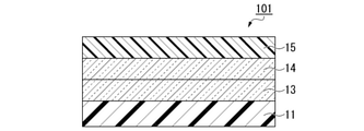
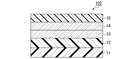
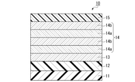
- the antifouling layer 15 differs depending on the use and configuration of the optical laminate.
- the average length RSm of the elements of the antifouling layer 15 is preferably 55 nm or more, for example. It is more preferably 90 nm or less.
- the average length RSm of the elements of the antifouling layer referred to here reflects the average length of the elements of the optical functional layer 14.
- the average length RSm of the elements of the antifouling layer 15 referred to here is a value before the scratch resistance test is performed.
- L0 * , a0 * , and b0 * are the values before the scratch resistance test
- L1 * , a1 * , and b1 * are the values after the scratch resistance test.
- the transparent base material 11 having the adhesion layer 13 and the optical functional layer 14 formed on the hard coat layer 12 is sent out to the pretreatment device 2B by the rotation of the film forming roll 25 and the guide roll 22.
- a second surface treatment step is performed as a pretreatment for the surface on which the antifouling layer 15 is formed.
- the transparent base material 11 on which the optical functional layer 14 is formed obtained by the optical functional layer forming step is continuously subjected to the second surface treatment while being maintained under reduced pressure without being exposed to the atmosphere. Perform the process.
- SR610 Polyethylene glycol diacrylate, average molecular weight of polyethylene glycol chain 600
- CN968 Hex-functional aliphatic urethane acrylate with polyester skeleton
- Irgacure 184 1-hydroxy-cyclohexyl-phenyl-ketone
- Example 9 the second surface treatment step was performed with an output of 1.0 kW, and the integrated output was 1086 W ⁇ min / m 2 .
- the film thickness of the antifouling layer was 5.0 nm.
- Example 10 was different from Example 9 in that the second surface treatment step was performed at an output of 1.5 kW, and the integrated output was 1629 W ⁇ min / m 2 .
- Example 11 was different from Example 9 in that the second surface treatment step was performed at an output of 0.5 kW, and the integrated output was 543 W ⁇ min / m 2 .
- Example 12 is different from Example 9 in that the film thickness of the antifouling layer is 4.0 nm.
- an alkoxysilane compound having a perfluoropolyether group (KY-1901, manufactured by Shin-Etsu Chemical Co., Ltd.) was used as a fluorine solvent (Florinate FC-3283: manufactured by 3M Japan Co., Ltd.) at a concentration of 0. The one diluted to 1% by mass was used. The antifouling agent was applied so that the thickness after drying was the film thickness shown in Tables 3A and 3B.
- Drop amount of each reagent 2.0 ⁇ L Measurement temperature: 25 ° C
- the contact angle after 4 seconds after dropping each reagent was measured at any 10 points on the surface of the test piece, and the average value was taken as the contact angle of oleic acid, n-hexadecane, and diiodomethane.
- X-ray Photoelectron Spectroscopy Electrode Spectroscopy for Chemical Analysis, ESCA
- PHI5000 VersaProb * eIII manufactured by ULVAC FI Co., Ltd.
- X-ray fluorescence X-ray fluorescence
Landscapes
- Chemical & Material Sciences (AREA)
- Engineering & Computer Science (AREA)
- Chemical Kinetics & Catalysis (AREA)
- Organic Chemistry (AREA)
- Materials Engineering (AREA)
- Mechanical Engineering (AREA)
- Physics & Mathematics (AREA)
- Metallurgy (AREA)
- General Physics & Mathematics (AREA)
- Optics & Photonics (AREA)
- Inorganic Chemistry (AREA)
- Health & Medical Sciences (AREA)
- Wood Science & Technology (AREA)
- Life Sciences & Earth Sciences (AREA)
- Manufacturing & Machinery (AREA)
- Ophthalmology & Optometry (AREA)
- Crystallography & Structural Chemistry (AREA)
- Surface Treatment Of Optical Elements (AREA)
- Laminated Bodies (AREA)
- Physical Vapour Deposition (AREA)
- Optical Filters (AREA)
- Medicinal Chemistry (AREA)
- Polymers & Plastics (AREA)
- Electroluminescent Light Sources (AREA)
Priority Applications (5)
| Application Number | Priority Date | Filing Date | Title |
|---|---|---|---|
| CN202180051438.0A CN115917366A (zh) | 2020-09-10 | 2021-09-08 | 光学层叠体、物品、光学层叠体的制造方法 |
| EP21866786.3A EP4212921A4 (en) | 2020-09-10 | 2021-09-08 | OPTICAL LAMINATE, ARTICLE AND METHOD FOR PRODUCING OPTICAL LAMINATE |
| KR1020227044278A KR102731218B1 (ko) | 2020-09-10 | 2021-09-08 | 광학 적층체, 물품, 광학 적층체의 제조 방법 |
| KR1020247037476A KR102896271B1 (ko) | 2020-09-10 | 2021-09-08 | 광학 적층체, 물품, 광학 적층체의 제조 방법 |
| US18/044,297 US20230324584A1 (en) | 2020-09-10 | 2021-09-08 | Optical laminate, article, and production method for optical laminate |
Applications Claiming Priority (2)
| Application Number | Priority Date | Filing Date | Title |
|---|---|---|---|
| JP2020-151806 | 2020-09-10 | ||
| JP2020151806 | 2020-09-10 |
Publications (1)
| Publication Number | Publication Date |
|---|---|
| WO2022054827A1 true WO2022054827A1 (ja) | 2022-03-17 |
Family
ID=80631602
Family Applications (2)
| Application Number | Title | Priority Date | Filing Date |
|---|---|---|---|
| PCT/JP2021/032978 Ceased WO2022054827A1 (ja) | 2020-09-10 | 2021-09-08 | 光学積層体、物品、光学積層体の製造方法 |
| PCT/JP2021/032991 Ceased WO2022054828A1 (ja) | 2020-09-10 | 2021-09-08 | 光学積層体の製造方法 |
Family Applications After (1)
| Application Number | Title | Priority Date | Filing Date |
|---|---|---|---|
| PCT/JP2021/032991 Ceased WO2022054828A1 (ja) | 2020-09-10 | 2021-09-08 | 光学積層体の製造方法 |
Country Status (7)
| Country | Link |
|---|---|
| US (2) | US12496792B2 (enExample) |
| EP (2) | EP4212922A4 (enExample) |
| JP (6) | JP7204849B2 (enExample) |
| KR (4) | KR102730596B1 (enExample) |
| CN (2) | CN115917366A (enExample) |
| TW (2) | TWI885203B (enExample) |
| WO (2) | WO2022054827A1 (enExample) |
Cited By (1)
| Publication number | Priority date | Publication date | Assignee | Title |
|---|---|---|---|---|
| WO2025177961A1 (ja) * | 2024-02-19 | 2025-08-28 | デクセリアルズ株式会社 | 光学積層体、光学積層体の製造方法及び物品 |
Families Citing this family (2)
| Publication number | Priority date | Publication date | Assignee | Title |
|---|---|---|---|---|
| JP2023167531A (ja) * | 2022-05-12 | 2023-11-24 | デクセリアルズ株式会社 | 光学積層体及び物品 |
| CN120366699B (zh) * | 2025-06-20 | 2025-09-16 | 吉林省巨程智造光电技术有限公司 | 一种半导体制造用纳米光学镜片的多层镀膜方法及应用 |
Citations (17)
| Publication number | Priority date | Publication date | Assignee | Title |
|---|---|---|---|---|
| JPH0242970B2 (enExample) | 1985-04-02 | 1990-09-26 | ||
| JP2000308846A (ja) * | 1999-04-26 | 2000-11-07 | Toppan Printing Co Ltd | 防汚層の形成方法 |
| JP2005301208A (ja) | 2004-03-17 | 2005-10-27 | Seiko Epson Corp | 防汚性光学物品の製造方法 |
| JP2006175438A (ja) | 2005-12-22 | 2006-07-06 | Toppan Printing Co Ltd | 防汚層の形成方法 |
| JP2009109850A (ja) * | 2007-10-31 | 2009-05-21 | Toppan Printing Co Ltd | 反射防止フィルム及びその製造方法並びに反射防止フィルムを用いた偏光板及びその製造方法 |
| JP2010191144A (ja) * | 2009-02-18 | 2010-09-02 | Toppan Printing Co Ltd | 反射防止フィルム |
| CN105835465A (zh) * | 2015-01-13 | 2016-08-10 | 南昌欧菲光学技术有限公司 | 增透防指纹叠层及其制作方法 |
| JP2016224443A (ja) * | 2015-05-27 | 2016-12-28 | デクセリアルズ株式会社 | 積層薄膜、及び積層薄膜の製造方法 |
| JP2017227898A (ja) * | 2016-06-17 | 2017-12-28 | 日東電工株式会社 | 反射防止フィルムおよびその製造方法、ならびに反射防止層付き偏光板 |
| WO2018193742A1 (ja) * | 2017-04-20 | 2018-10-25 | 信越化学工業株式会社 | 反射防止部材及びその製造方法 |
| WO2019064969A1 (ja) * | 2017-09-28 | 2019-04-04 | 日東電工株式会社 | 反射防止フィルムおよびその製造方法、ならびに反射防止層付き偏光板 |
| WO2019078313A1 (ja) | 2017-10-19 | 2019-04-25 | Agc株式会社 | 透明基板積層体およびその製造方法 |
| WO2020027037A1 (ja) * | 2018-07-31 | 2020-02-06 | 日本電産株式会社 | コーティング方法、光学部品、及びレンズアッセンブリ |
| JP2020151806A (ja) | 2019-03-20 | 2020-09-24 | 株式会社東芝 | 研磨装置及び研磨方法 |
| WO2021106797A1 (ja) * | 2019-11-25 | 2021-06-03 | 日東電工株式会社 | 反射防止フィルムおよび画像表示装置 |
| WO2021177348A1 (ja) * | 2020-03-04 | 2021-09-10 | デクセリアルズ株式会社 | 光学積層体の製造方法 |
| WO2021177350A1 (ja) * | 2020-03-04 | 2021-09-10 | デクセリアルズ株式会社 | 光学積層体、物品、光学積層体の製造方法 |
Family Cites Families (57)
| Publication number | Priority date | Publication date | Assignee | Title |
|---|---|---|---|---|
| JP3360898B2 (ja) | 1993-10-05 | 2003-01-07 | 日東電工株式会社 | 反射防止部材の製造方法及び偏光板 |
| JPH10133001A (ja) | 1996-11-01 | 1998-05-22 | Nikon Corp | 新規な撥水処理されたレンズ |
| JP3604055B2 (ja) | 1997-05-07 | 2004-12-22 | 株式会社ダイオー | 表面処理方法およびエチレン−テトラフルオロエチレン系共重合体成形体 |
| EP0974560B2 (en) * | 1997-12-09 | 2015-12-30 | Nippon Sheet Glass Co., Ltd. | Antireflection glass plate, process for producing the same, and antireflection coating composition |
| JP4733798B2 (ja) | 1998-01-31 | 2011-07-27 | 凸版印刷株式会社 | 防汚剤、防汚層の形成方法、光学部材、反射防止光学部材、光学機能性部材及び表示装置 |
| JPH11258405A (ja) | 1998-03-12 | 1999-09-24 | Toppan Printing Co Ltd | 反射防止フィルム |
| JP2002243906A (ja) * | 2001-02-21 | 2002-08-28 | Toppan Printing Co Ltd | 反射防止積層体及びその製造方法 |
| JP4765185B2 (ja) | 2001-03-28 | 2011-09-07 | Tdk株式会社 | 物体表面の防汚処理方法及び防汚処理された物体 |
| JP4834939B2 (ja) | 2001-08-28 | 2011-12-14 | ソニー株式会社 | 反射防止フィルム |
| JP2004021550A (ja) | 2002-06-14 | 2004-01-22 | Sony Corp | タッチパネル、表示体、反射防止フィルム及びこれらの製造方法 |
| JP2004138662A (ja) | 2002-10-15 | 2004-05-13 | Fuji Photo Film Co Ltd | 反射防止膜、反射防止フィルムおよび画像表示装置 |
| JP2004170962A (ja) | 2002-11-06 | 2004-06-17 | Pentax Corp | 反射防止眼鏡レンズ及びその製造方法 |
| JP2004170500A (ja) | 2002-11-18 | 2004-06-17 | Seiko Epson Corp | プラスチックレンズ及びその製造方法 |
| JP2004258469A (ja) | 2003-02-27 | 2004-09-16 | Konica Minolta Holdings Inc | 反射防止フィルム、反射防止フィルムの製造方法、偏光板及び表示装置 |
| US7217440B2 (en) | 2003-06-13 | 2007-05-15 | Essilor International Compagnie Generale D'optique | Process for replacing an initial outermost coating layer of a coated optical lens with a different coating layer or by depositing thereon a different coating layer |
| TWI388876B (zh) | 2003-12-26 | 2013-03-11 | Fujifilm Corp | 抗反射膜、偏光板,其製造方法,液晶顯示元件,液晶顯示裝置,及影像顯示裝置 |
| JP2006220733A (ja) | 2005-02-08 | 2006-08-24 | Fuji Photo Film Co Ltd | 反射防止フィルム、偏光板、及びそれを用いた画像表示装置 |
| US8945684B2 (en) | 2005-11-04 | 2015-02-03 | Essilor International (Compagnie Generale D'optique) | Process for coating an article with an anti-fouling surface coating by vacuum evaporation |
| JP2007194109A (ja) | 2006-01-20 | 2007-08-02 | Toppan Printing Co Ltd | 導電性積層体、光学機能性フィルタおよび光学表示装置 |
| JP2008062460A (ja) | 2006-09-06 | 2008-03-21 | Konica Minolta Holdings Inc | 光学フィルムとそれを用いた画像表示素子 |
| JP4964021B2 (ja) | 2007-05-15 | 2012-06-27 | 旭化成ケミカルズ株式会社 | 防汚層の形成方法 |
| JP5217887B2 (ja) | 2008-01-28 | 2013-06-19 | セイコーエプソン株式会社 | 光学物品 |
| US8399110B2 (en) | 2008-05-29 | 2013-03-19 | Corning Incorporated | Adhesive, hermetic oxide films for metal fluoride optics and method of making same |
| JP2011013654A (ja) | 2008-10-23 | 2011-01-20 | Seiko Epson Corp | 多層反射防止層およびその製造方法、プラスチックレンズ |
| JP5245893B2 (ja) * | 2009-02-13 | 2013-07-24 | 凸版印刷株式会社 | 多層フィルムおよびその製造方法 |
| CN102012532B (zh) * | 2009-09-03 | 2015-05-20 | 株式会社巴川制纸所 | 光学层叠体、偏振片及使用其的显示装置 |
| JP5523066B2 (ja) * | 2009-11-17 | 2014-06-18 | ホーヤ レンズ マニュファクチャリング フィリピン インク | 光学物品の製造方法 |
| EP2530112A4 (en) | 2010-01-29 | 2014-01-15 | Asahi Glass Co Ltd | SURFACE TREATMENT METHOD FOR A FLUOROE RESIN BODY AND FLUORIDE RESIN BODY |
| US8709582B2 (en) * | 2010-07-30 | 2014-04-29 | Essilor International | Optical article including an antireflecting coating having antifog properties and process for making same |
| KR101362967B1 (ko) * | 2012-01-11 | 2014-02-13 | 정상희 | 플라즈마 처리된 옵티컬 본딩용 실리콘 점착 시트 및 그 제조 방법 |
| JP5938280B2 (ja) | 2012-06-22 | 2016-06-22 | 日華化学株式会社 | パーフルオロポリエーテル変性シラン化合物、防汚性被膜形成用組成物、防汚性被膜、およびこの被膜を有する物品 |
| DE112014000955T5 (de) | 2013-02-22 | 2015-11-05 | Asahi Glass Company, Limited | Optische Komponente |
| WO2014199991A1 (ja) | 2013-06-11 | 2014-12-18 | 日本電気硝子株式会社 | カバー部材、表示装置及びカバー部材の製造方法 |
| WO2015159839A1 (ja) | 2014-04-15 | 2015-10-22 | 旭硝子株式会社 | 反射防止積層体およびその製造方法 |
| JP6661286B2 (ja) | 2014-06-30 | 2020-03-11 | 三星電子株式会社Samsung Electronics Co.,Ltd. | 樹脂膜、光学部材および偏光部材 |
| CN107107543B (zh) | 2014-10-30 | 2021-07-20 | Agc株式会社 | 带防污膜的基体 |
| KR101807208B1 (ko) | 2015-08-18 | 2017-12-08 | 주식회사 엘지화학 | 저굴절층 및 이를 포함하는 반사 방지 필름 |
| WO2017030046A1 (ja) | 2015-08-19 | 2017-02-23 | 旭硝子株式会社 | 積層体 |
| US9733488B2 (en) | 2015-11-16 | 2017-08-15 | Younger Mfg. Co. | Composite constructed optical lens |
| WO2017126300A1 (ja) | 2016-01-19 | 2017-07-27 | 株式会社ニコン・エシロール | 眼鏡レンズ |
| JP6787673B2 (ja) | 2016-02-15 | 2020-11-18 | デクセリアルズ株式会社 | 反射防止フィルム、及び反射防止フィルムの製造方法 |
| JP2017161893A (ja) * | 2016-03-03 | 2017-09-14 | 日東電工株式会社 | 光学積層体 |
| JP6934308B2 (ja) | 2016-04-01 | 2021-09-15 | 日東電工株式会社 | 光透過性フィルム |
| CN105779943A (zh) | 2016-05-05 | 2016-07-20 | 厦门建霖工业有限公司 | 一种物理气相沉积氟硅烷制备疏水膜的方法 |
| JP2018004921A (ja) | 2016-06-30 | 2018-01-11 | ホヤ レンズ タイランド リミテッドHOYA Lens Thailand Ltd | 眼鏡レンズ及び眼鏡レンズの製造方法 |
| JP6746410B2 (ja) | 2016-07-13 | 2020-08-26 | 大日本印刷株式会社 | 光学積層体 |
| CN115079316B (zh) | 2017-05-08 | 2024-03-26 | 康宁股份有限公司 | 光学和耐划痕涂层上具有耐用润滑防指纹涂层的玻璃、玻璃陶瓷和陶瓷制品及其制造方法 |
| WO2019035398A1 (ja) | 2017-08-15 | 2019-02-21 | 大日本印刷株式会社 | 光学フィルム、偏光板、および画像表示装置 |
| JP2020148787A (ja) | 2018-06-06 | 2020-09-17 | Agc株式会社 | 透明部材 |
| JP6999370B2 (ja) | 2017-11-06 | 2022-01-18 | 日東電工株式会社 | 反射防止層付偏光板およびその製造方法 |
| JP7121479B2 (ja) | 2017-11-14 | 2022-08-18 | 株式会社トッパンTomoegawaオプティカルフィルム | 光学積層体、偏光板及び表示装置 |
| WO2019107036A1 (ja) | 2017-11-29 | 2019-06-06 | 日東電工株式会社 | ハードコートフィルム、光学積層体および画像表示装置 |
| CN208110086U (zh) | 2018-01-25 | 2018-11-16 | 江苏新光镭射包装材料股份有限公司 | 耐指纹高遮蔽率的光学反射膜 |
| JP2020037248A (ja) | 2018-09-03 | 2020-03-12 | 住友化学株式会社 | 積層体及びその製造方法 |
| JP6542970B2 (ja) | 2018-10-10 | 2019-07-10 | デクセリアルズ株式会社 | 反射防止膜の製造方法 |
| JP7089609B2 (ja) | 2020-03-04 | 2022-06-22 | デクセリアルズ株式会社 | 光学積層体、物品、光学積層体の製造方法 |
| US20230191732A1 (en) | 2020-07-17 | 2023-06-22 | Dexerials Corporation | Method for producing optical multilayer body |
-
2021
- 2021-09-08 TW TW110133457A patent/TWI885203B/zh active
- 2021-09-08 KR KR1020227044279A patent/KR102730596B1/ko active Active
- 2021-09-08 EP EP21866787.1A patent/EP4212922A4/en active Pending
- 2021-09-08 KR KR1020227044278A patent/KR102731218B1/ko active Active
- 2021-09-08 WO PCT/JP2021/032978 patent/WO2022054827A1/ja not_active Ceased
- 2021-09-08 WO PCT/JP2021/032991 patent/WO2022054828A1/ja not_active Ceased
- 2021-09-08 KR KR1020247037476A patent/KR102896271B1/ko active Active
- 2021-09-08 KR KR1020247037154A patent/KR20240163762A/ko active Pending
- 2021-09-08 US US18/044,295 patent/US12496792B2/en active Active
- 2021-09-08 TW TW110133458A patent/TWI890852B/zh active
- 2021-09-08 JP JP2021146047A patent/JP7204849B2/ja active Active
- 2021-09-08 JP JP2021146049A patent/JP7204850B2/ja active Active
- 2021-09-08 CN CN202180051438.0A patent/CN115917366A/zh active Pending
- 2021-09-08 EP EP21866786.3A patent/EP4212921A4/en active Pending
- 2021-09-08 US US18/044,297 patent/US20230324584A1/en active Pending
- 2021-09-08 CN CN202180054441.8A patent/CN116075750A/zh active Pending
-
2022
- 2022-12-28 JP JP2022211761A patent/JP7273238B2/ja active Active
- 2022-12-28 JP JP2022212380A patent/JP7273239B2/ja active Active
-
2023
- 2023-04-27 JP JP2023073426A patent/JP7791854B2/ja active Active
- 2023-04-27 JP JP2023073343A patent/JP7791853B2/ja active Active
Patent Citations (17)
| Publication number | Priority date | Publication date | Assignee | Title |
|---|---|---|---|---|
| JPH0242970B2 (enExample) | 1985-04-02 | 1990-09-26 | ||
| JP2000308846A (ja) * | 1999-04-26 | 2000-11-07 | Toppan Printing Co Ltd | 防汚層の形成方法 |
| JP2005301208A (ja) | 2004-03-17 | 2005-10-27 | Seiko Epson Corp | 防汚性光学物品の製造方法 |
| JP2006175438A (ja) | 2005-12-22 | 2006-07-06 | Toppan Printing Co Ltd | 防汚層の形成方法 |
| JP2009109850A (ja) * | 2007-10-31 | 2009-05-21 | Toppan Printing Co Ltd | 反射防止フィルム及びその製造方法並びに反射防止フィルムを用いた偏光板及びその製造方法 |
| JP2010191144A (ja) * | 2009-02-18 | 2010-09-02 | Toppan Printing Co Ltd | 反射防止フィルム |
| CN105835465A (zh) * | 2015-01-13 | 2016-08-10 | 南昌欧菲光学技术有限公司 | 增透防指纹叠层及其制作方法 |
| JP2016224443A (ja) * | 2015-05-27 | 2016-12-28 | デクセリアルズ株式会社 | 積層薄膜、及び積層薄膜の製造方法 |
| JP2017227898A (ja) * | 2016-06-17 | 2017-12-28 | 日東電工株式会社 | 反射防止フィルムおよびその製造方法、ならびに反射防止層付き偏光板 |
| WO2018193742A1 (ja) * | 2017-04-20 | 2018-10-25 | 信越化学工業株式会社 | 反射防止部材及びその製造方法 |
| WO2019064969A1 (ja) * | 2017-09-28 | 2019-04-04 | 日東電工株式会社 | 反射防止フィルムおよびその製造方法、ならびに反射防止層付き偏光板 |
| WO2019078313A1 (ja) | 2017-10-19 | 2019-04-25 | Agc株式会社 | 透明基板積層体およびその製造方法 |
| WO2020027037A1 (ja) * | 2018-07-31 | 2020-02-06 | 日本電産株式会社 | コーティング方法、光学部品、及びレンズアッセンブリ |
| JP2020151806A (ja) | 2019-03-20 | 2020-09-24 | 株式会社東芝 | 研磨装置及び研磨方法 |
| WO2021106797A1 (ja) * | 2019-11-25 | 2021-06-03 | 日東電工株式会社 | 反射防止フィルムおよび画像表示装置 |
| WO2021177348A1 (ja) * | 2020-03-04 | 2021-09-10 | デクセリアルズ株式会社 | 光学積層体の製造方法 |
| WO2021177350A1 (ja) * | 2020-03-04 | 2021-09-10 | デクセリアルズ株式会社 | 光学積層体、物品、光学積層体の製造方法 |
Non-Patent Citations (1)
| Title |
|---|
| See also references of EP4212921A4 |
Cited By (1)
| Publication number | Priority date | Publication date | Assignee | Title |
|---|---|---|---|---|
| WO2025177961A1 (ja) * | 2024-02-19 | 2025-08-28 | デクセリアルズ株式会社 | 光学積層体、光学積層体の製造方法及び物品 |
Also Published As
Similar Documents
| Publication | Publication Date | Title |
|---|---|---|
| JP7228067B2 (ja) | 光学積層体、物品、光学積層体の製造方法 | |
| JP7089609B2 (ja) | 光学積層体、物品、光学積層体の製造方法 | |
| JP7101297B2 (ja) | 光学積層体、物品、光学積層体の製造方法 | |
| JP7089610B2 (ja) | 光学積層体の製造方法 | |
| JP7273239B2 (ja) | 光学積層体、物品、光学積層体の製造方法 | |
| JP7303954B2 (ja) | 光学積層体の製造方法 | |
| WO2022014701A1 (ja) | 光学積層体の製造方法 | |
| KR102735288B1 (ko) | 광학 적층체, 물품, 광학 적층체의 제조 방법 | |
| JP7248830B2 (ja) | 光学積層体の製造方法 |
Legal Events
| Date | Code | Title | Description |
|---|---|---|---|
| 121 | Ep: the epo has been informed by wipo that ep was designated in this application |
Ref document number: 21866786 Country of ref document: EP Kind code of ref document: A1 |
|
| ENP | Entry into the national phase |
Ref document number: 20227044278 Country of ref document: KR Kind code of ref document: A |
|
| WWE | Wipo information: entry into national phase |
Ref document number: 202317015235 Country of ref document: IN |
|
| NENP | Non-entry into the national phase |
Ref country code: DE |
|
| ENP | Entry into the national phase |
Ref document number: 2021866786 Country of ref document: EP Effective date: 20230411 |