WO2022054827A1 - Stratifié optique, article et procédé de production de stratifié optique - Google Patents
Stratifié optique, article et procédé de production de stratifié optique Download PDFInfo
- Publication number
- WO2022054827A1 WO2022054827A1 PCT/JP2021/032978 JP2021032978W WO2022054827A1 WO 2022054827 A1 WO2022054827 A1 WO 2022054827A1 JP 2021032978 W JP2021032978 W JP 2021032978W WO 2022054827 A1 WO2022054827 A1 WO 2022054827A1
- Authority
- WO
- WIPO (PCT)
- Prior art keywords
- layer
- optical
- antifouling
- optical laminate
- optical functional
- Prior art date
Links
- 230000003287 optical effect Effects 0.000 title claims abstract description 436
- 238000004519 manufacturing process Methods 0.000 title claims description 62
- 239000010410 layer Substances 0.000 claims abstract description 551
- 230000003373 anti-fouling effect Effects 0.000 claims abstract description 227
- 239000002346 layers by function Substances 0.000 claims abstract description 208
- 239000000463 material Substances 0.000 claims abstract description 84
- XLYOFNOQVPJJNP-UHFFFAOYSA-N water Chemical compound O XLYOFNOQVPJJNP-UHFFFAOYSA-N 0.000 claims abstract description 32
- HEMHJVSKTPXQMS-UHFFFAOYSA-M Sodium hydroxide Chemical compound [OH-].[Na+] HEMHJVSKTPXQMS-UHFFFAOYSA-M 0.000 claims abstract description 30
- 239000007788 liquid Substances 0.000 claims abstract description 11
- 239000002985 plastic film Substances 0.000 claims abstract description 9
- 229920006255 plastic film Polymers 0.000 claims abstract description 9
- 239000010408 film Substances 0.000 claims description 151
- 238000012360 testing method Methods 0.000 claims description 82
- 238000000034 method Methods 0.000 claims description 72
- 238000004381 surface treatment Methods 0.000 claims description 61
- YCKRFDGAMUMZLT-UHFFFAOYSA-N Fluorine atom Chemical compound [F] YCKRFDGAMUMZLT-UHFFFAOYSA-N 0.000 claims description 56
- 229910052731 fluorine Inorganic materials 0.000 claims description 56
- 239000011737 fluorine Substances 0.000 claims description 56
- 230000008859 change Effects 0.000 claims description 54
- 230000003746 surface roughness Effects 0.000 claims description 50
- 238000011282 treatment Methods 0.000 claims description 47
- 208000028659 discharge Diseases 0.000 claims description 46
- 238000004544 sputter deposition Methods 0.000 claims description 42
- 239000002904 solvent Substances 0.000 claims description 14
- 239000002699 waste material Substances 0.000 claims description 14
- 229910000831 Steel Inorganic materials 0.000 claims description 13
- 239000010959 steel Substances 0.000 claims description 13
- 210000002268 wool Anatomy 0.000 claims description 13
- 239000004744 fabric Substances 0.000 claims description 12
- 238000002441 X-ray diffraction Methods 0.000 claims description 11
- 150000002894 organic compounds Chemical class 0.000 claims description 10
- 229910052751 metal Inorganic materials 0.000 claims description 8
- 239000002184 metal Substances 0.000 claims description 8
- 239000012790 adhesive layer Substances 0.000 claims description 7
- 230000035699 permeability Effects 0.000 claims description 7
- 239000010409 thin film Substances 0.000 claims description 4
- 238000001771 vacuum deposition Methods 0.000 claims description 4
- 239000007864 aqueous solution Substances 0.000 claims description 3
- 230000001678 irradiating effect Effects 0.000 claims description 3
- 125000001153 fluoro group Chemical group F* 0.000 claims description 2
- 238000005406 washing Methods 0.000 claims description 2
- 238000007740 vapor deposition Methods 0.000 abstract description 33
- 230000005540 biological transmission Effects 0.000 abstract description 4
- 238000010030 laminating Methods 0.000 abstract description 4
- 239000002585 base Substances 0.000 description 55
- 230000000052 comparative effect Effects 0.000 description 49
- 229920005989 resin Polymers 0.000 description 42
- 239000011347 resin Substances 0.000 description 42
- NIXOWILDQLNWCW-UHFFFAOYSA-M Acrylate Chemical compound [O-]C(=O)C=C NIXOWILDQLNWCW-UHFFFAOYSA-M 0.000 description 30
- 239000003513 alkali Substances 0.000 description 23
- 239000007789 gas Substances 0.000 description 22
- 239000000758 substrate Substances 0.000 description 22
- 238000005259 measurement Methods 0.000 description 19
- 230000008569 process Effects 0.000 description 18
- 239000000945 filler Substances 0.000 description 17
- 229920002284 Cellulose triacetate Polymers 0.000 description 15
- NNLVGZFZQQXQNW-ADJNRHBOSA-N [(2r,3r,4s,5r,6s)-4,5-diacetyloxy-3-[(2s,3r,4s,5r,6r)-3,4,5-triacetyloxy-6-(acetyloxymethyl)oxan-2-yl]oxy-6-[(2r,3r,4s,5r,6s)-4,5,6-triacetyloxy-2-(acetyloxymethyl)oxan-3-yl]oxyoxan-2-yl]methyl acetate Chemical compound O([C@@H]1O[C@@H]([C@H]([C@H](OC(C)=O)[C@H]1OC(C)=O)O[C@H]1[C@@H]([C@@H](OC(C)=O)[C@H](OC(C)=O)[C@@H](COC(C)=O)O1)OC(C)=O)COC(=O)C)[C@@H]1[C@@H](COC(C)=O)O[C@@H](OC(C)=O)[C@H](OC(C)=O)[C@H]1OC(C)=O NNLVGZFZQQXQNW-ADJNRHBOSA-N 0.000 description 15
- 239000012298 atmosphere Substances 0.000 description 15
- 239000002245 particle Substances 0.000 description 15
- 238000004804 winding Methods 0.000 description 15
- 230000000694 effects Effects 0.000 description 14
- VYPSYNLAJGMNEJ-UHFFFAOYSA-N Silicium dioxide Chemical compound O=[Si]=O VYPSYNLAJGMNEJ-UHFFFAOYSA-N 0.000 description 13
- 230000015572 biosynthetic process Effects 0.000 description 12
- 238000000576 coating method Methods 0.000 description 12
- 239000000126 substance Substances 0.000 description 12
- 229910004298 SiO 2 Inorganic materials 0.000 description 11
- 238000010438 heat treatment Methods 0.000 description 11
- 238000000427 thin-film deposition Methods 0.000 description 11
- QVGXLLKOCUKJST-UHFFFAOYSA-N atomic oxygen Chemical compound [O] QVGXLLKOCUKJST-UHFFFAOYSA-N 0.000 description 10
- 150000001875 compounds Chemical class 0.000 description 10
- 239000001301 oxygen Substances 0.000 description 10
- 229910052760 oxygen Inorganic materials 0.000 description 10
- 239000002519 antifouling agent Substances 0.000 description 9
- 239000011230 binding agent Substances 0.000 description 9
- XKRFYHLGVUSROY-UHFFFAOYSA-N Argon Chemical compound [Ar] XKRFYHLGVUSROY-UHFFFAOYSA-N 0.000 description 8
- 239000011248 coating agent Substances 0.000 description 8
- 238000005096 rolling process Methods 0.000 description 8
- 239000003153 chemical reaction reagent Substances 0.000 description 7
- 230000006837 decompression Effects 0.000 description 7
- 239000004745 nonwoven fabric Substances 0.000 description 7
- 229910052814 silicon oxide Inorganic materials 0.000 description 7
- 238000002834 transmittance Methods 0.000 description 7
- 229920000178 Acrylic resin Polymers 0.000 description 6
- 239000004925 Acrylic resin Substances 0.000 description 6
- PPBRXRYQALVLMV-UHFFFAOYSA-N Styrene Chemical compound C=CC1=CC=CC=C1 PPBRXRYQALVLMV-UHFFFAOYSA-N 0.000 description 6
- 238000004833 X-ray photoelectron spectroscopy Methods 0.000 description 6
- PNEYBMLMFCGWSK-UHFFFAOYSA-N aluminium oxide Inorganic materials [O-2].[O-2].[O-2].[Al+3].[Al+3] PNEYBMLMFCGWSK-UHFFFAOYSA-N 0.000 description 6
- DCAYPVUWAIABOU-UHFFFAOYSA-N hexadecane Chemical compound CCCCCCCCCCCCCCCC DCAYPVUWAIABOU-UHFFFAOYSA-N 0.000 description 6
- 229910044991 metal oxide Inorganic materials 0.000 description 6
- 150000004706 metal oxides Chemical class 0.000 description 6
- 239000012788 optical film Substances 0.000 description 6
- 239000012779 reinforcing material Substances 0.000 description 6
- 239000000243 solution Substances 0.000 description 6
- 238000004506 ultrasonic cleaning Methods 0.000 description 6
- 229920002678 cellulose Polymers 0.000 description 5
- 239000011521 glass Substances 0.000 description 5
- 239000000203 mixture Substances 0.000 description 5
- 239000013077 target material Substances 0.000 description 5
- XLOMVQKBTHCTTD-UHFFFAOYSA-N Zinc monoxide Chemical compound [Zn]=O XLOMVQKBTHCTTD-UHFFFAOYSA-N 0.000 description 4
- NIXOWILDQLNWCW-UHFFFAOYSA-N acrylic acid group Chemical group C(C=C)(=O)O NIXOWILDQLNWCW-UHFFFAOYSA-N 0.000 description 4
- 229910052786 argon Inorganic materials 0.000 description 4
- 239000001913 cellulose Substances 0.000 description 4
- 238000004140 cleaning Methods 0.000 description 4
- 238000010894 electron beam technology Methods 0.000 description 4
- 230000001771 impaired effect Effects 0.000 description 4
- 239000010702 perfluoropolyether Substances 0.000 description 4
- 229920001225 polyester resin Polymers 0.000 description 4
- 239000000047 product Substances 0.000 description 4
- 239000011342 resin composition Substances 0.000 description 4
- 239000002356 single layer Substances 0.000 description 4
- WRIDQFICGBMAFQ-UHFFFAOYSA-N (E)-8-Octadecenoic acid Natural products CCCCCCCCCC=CCCCCCCC(O)=O WRIDQFICGBMAFQ-UHFFFAOYSA-N 0.000 description 3
- LQJBNNIYVWPHFW-UHFFFAOYSA-N 20:1omega9c fatty acid Natural products CCCCCCCCCCC=CCCCCCCCC(O)=O LQJBNNIYVWPHFW-UHFFFAOYSA-N 0.000 description 3
- QSBYPNXLFMSGKH-UHFFFAOYSA-N 9-Heptadecensaeure Natural products CCCCCCCC=CCCCCCCCC(O)=O QSBYPNXLFMSGKH-UHFFFAOYSA-N 0.000 description 3
- MYMOFIZGZYHOMD-UHFFFAOYSA-N Dioxygen Chemical compound O=O MYMOFIZGZYHOMD-UHFFFAOYSA-N 0.000 description 3
- 239000005642 Oleic acid Substances 0.000 description 3
- ZQPPMHVWECSIRJ-UHFFFAOYSA-N Oleic acid Natural products CCCCCCCCC=CCCCCCCCC(O)=O ZQPPMHVWECSIRJ-UHFFFAOYSA-N 0.000 description 3
- GWEVSGVZZGPLCZ-UHFFFAOYSA-N Titan oxide Chemical compound O=[Ti]=O GWEVSGVZZGPLCZ-UHFFFAOYSA-N 0.000 description 3
- 239000012670 alkaline solution Substances 0.000 description 3
- 229910052782 aluminium Inorganic materials 0.000 description 3
- 230000002950 deficient Effects 0.000 description 3
- MTHSVFCYNBDYFN-UHFFFAOYSA-N diethylene glycol Chemical compound OCCOCCO MTHSVFCYNBDYFN-UHFFFAOYSA-N 0.000 description 3
- NZZFYRREKKOMAT-UHFFFAOYSA-N diiodomethane Chemical compound ICI NZZFYRREKKOMAT-UHFFFAOYSA-N 0.000 description 3
- 229910001882 dioxygen Inorganic materials 0.000 description 3
- 238000007599 discharging Methods 0.000 description 3
- 238000001035 drying Methods 0.000 description 3
- -1 ethylhexyl Chemical group 0.000 description 3
- 238000001704 evaporation Methods 0.000 description 3
- 230000008020 evaporation Effects 0.000 description 3
- 230000006698 induction Effects 0.000 description 3
- 230000005865 ionizing radiation Effects 0.000 description 3
- QXJSBBXBKPUZAA-UHFFFAOYSA-N isooleic acid Natural products CCCCCCCC=CCCCCCCCCC(O)=O QXJSBBXBKPUZAA-UHFFFAOYSA-N 0.000 description 3
- 239000010955 niobium Substances 0.000 description 3
- ZQPPMHVWECSIRJ-KTKRTIGZSA-N oleic acid Chemical compound CCCCCCCC\C=C/CCCCCCCC(O)=O ZQPPMHVWECSIRJ-KTKRTIGZSA-N 0.000 description 3
- 230000001590 oxidative effect Effects 0.000 description 3
- 238000009832 plasma treatment Methods 0.000 description 3
- 229920000728 polyester Polymers 0.000 description 3
- 229920005672 polyolefin resin Polymers 0.000 description 3
- 229910052710 silicon Inorganic materials 0.000 description 3
- 238000009751 slip forming Methods 0.000 description 3
- 229920005992 thermoplastic resin Polymers 0.000 description 3
- 238000012546 transfer Methods 0.000 description 3
- 230000037303 wrinkles Effects 0.000 description 3
- 229910052726 zirconium Inorganic materials 0.000 description 3
- MYWOJODOMFBVCB-UHFFFAOYSA-N 1,2,6-trimethylphenanthrene Chemical compound CC1=CC=C2C3=CC(C)=CC=C3C=CC2=C1C MYWOJODOMFBVCB-UHFFFAOYSA-N 0.000 description 2
- TXBCBTDQIULDIA-UHFFFAOYSA-N 2-[[3-hydroxy-2,2-bis(hydroxymethyl)propoxy]methyl]-2-(hydroxymethyl)propane-1,3-diol Chemical compound OCC(CO)(CO)COCC(CO)(CO)CO TXBCBTDQIULDIA-UHFFFAOYSA-N 0.000 description 2
- QTBSBXVTEAMEQO-UHFFFAOYSA-M Acetate Chemical compound CC([O-])=O QTBSBXVTEAMEQO-UHFFFAOYSA-M 0.000 description 2
- 235000017166 Bambusa arundinacea Nutrition 0.000 description 2
- 235000017491 Bambusa tulda Nutrition 0.000 description 2
- 241001330002 Bambuseae Species 0.000 description 2
- IAYPIBMASNFSPL-UHFFFAOYSA-N Ethylene oxide Chemical compound C1CO1 IAYPIBMASNFSPL-UHFFFAOYSA-N 0.000 description 2
- 229920000877 Melamine resin Polymers 0.000 description 2
- 240000007594 Oryza sativa Species 0.000 description 2
- 235000007164 Oryza sativa Nutrition 0.000 description 2
- 235000015334 Phyllostachys viridis Nutrition 0.000 description 2
- 239000002202 Polyethylene glycol Substances 0.000 description 2
- GOOHAUXETOMSMM-UHFFFAOYSA-N Propylene oxide Chemical compound CC1CO1 GOOHAUXETOMSMM-UHFFFAOYSA-N 0.000 description 2
- XUIMIQQOPSSXEZ-UHFFFAOYSA-N Silicon Chemical compound [Si] XUIMIQQOPSSXEZ-UHFFFAOYSA-N 0.000 description 2
- MCMNRKCIXSYSNV-UHFFFAOYSA-N Zirconium dioxide Chemical compound O=[Zr]=O MCMNRKCIXSYSNV-UHFFFAOYSA-N 0.000 description 2
- HVVWZTWDBSEWIH-UHFFFAOYSA-N [2-(hydroxymethyl)-3-prop-2-enoyloxy-2-(prop-2-enoyloxymethyl)propyl] prop-2-enoate Chemical compound C=CC(=O)OCC(CO)(COC(=O)C=C)COC(=O)C=C HVVWZTWDBSEWIH-UHFFFAOYSA-N 0.000 description 2
- MPIAGWXWVAHQBB-UHFFFAOYSA-N [3-prop-2-enoyloxy-2-[[3-prop-2-enoyloxy-2,2-bis(prop-2-enoyloxymethyl)propoxy]methyl]-2-(prop-2-enoyloxymethyl)propyl] prop-2-enoate Chemical compound C=CC(=O)OCC(COC(=O)C=C)(COC(=O)C=C)COCC(COC(=O)C=C)(COC(=O)C=C)COC(=O)C=C MPIAGWXWVAHQBB-UHFFFAOYSA-N 0.000 description 2
- 239000011425 bamboo Substances 0.000 description 2
- 239000003795 chemical substances by application Substances 0.000 description 2
- 239000000470 constituent Substances 0.000 description 2
- 238000000151 deposition Methods 0.000 description 2
- 238000009792 diffusion process Methods 0.000 description 2
- 239000012153 distilled water Substances 0.000 description 2
- 238000005530 etching Methods 0.000 description 2
- 239000010419 fine particle Substances 0.000 description 2
- 238000007654 immersion Methods 0.000 description 2
- 230000006872 improvement Effects 0.000 description 2
- 229910010272 inorganic material Inorganic materials 0.000 description 2
- 239000011147 inorganic material Substances 0.000 description 2
- ZFSLODLOARCGLH-UHFFFAOYSA-N isocyanuric acid Chemical compound OC1=NC(O)=NC(O)=N1 ZFSLODLOARCGLH-UHFFFAOYSA-N 0.000 description 2
- 230000033001 locomotion Effects 0.000 description 2
- 238000001755 magnetron sputter deposition Methods 0.000 description 2
- 239000002121 nanofiber Substances 0.000 description 2
- 239000003921 oil Substances 0.000 description 2
- 125000000962 organic group Chemical group 0.000 description 2
- 230000003647 oxidation Effects 0.000 description 2
- 238000007254 oxidation reaction Methods 0.000 description 2
- 239000003973 paint Substances 0.000 description 2
- WXZMFSXDPGVJKK-UHFFFAOYSA-N pentaerythritol Chemical compound OCC(CO)(CO)CO WXZMFSXDPGVJKK-UHFFFAOYSA-N 0.000 description 2
- 230000002093 peripheral effect Effects 0.000 description 2
- 239000012466 permeate Substances 0.000 description 2
- 230000003863 physical function Effects 0.000 description 2
- 229920006122 polyamide resin Polymers 0.000 description 2
- 229920005668 polycarbonate resin Polymers 0.000 description 2
- 239000004431 polycarbonate resin Substances 0.000 description 2
- 239000004645 polyester resin Substances 0.000 description 2
- 229920001223 polyethylene glycol Polymers 0.000 description 2
- 230000002265 prevention Effects 0.000 description 2
- 238000012545 processing Methods 0.000 description 2
- 235000009566 rice Nutrition 0.000 description 2
- 239000010703 silicon Substances 0.000 description 2
- 239000000377 silicon dioxide Substances 0.000 description 2
- 125000003808 silyl group Chemical group [H][Si]([H])([H])[*] 0.000 description 2
- 239000002002 slurry Substances 0.000 description 2
- 238000000992 sputter etching Methods 0.000 description 2
- 229910001220 stainless steel Inorganic materials 0.000 description 2
- 239000010935 stainless steel Substances 0.000 description 2
- 229920001187 thermosetting polymer Polymers 0.000 description 2
- 239000012780 transparent material Substances 0.000 description 2
- 239000011787 zinc oxide Substances 0.000 description 2
- QNODIIQQMGDSEF-UHFFFAOYSA-N (1-hydroxycyclohexyl)-phenylmethanone Chemical compound C=1C=CC=CC=1C(=O)C1(O)CCCCC1 QNODIIQQMGDSEF-UHFFFAOYSA-N 0.000 description 1
- VZXTWGWHSMCWGA-UHFFFAOYSA-N 1,3,5-triazine-2,4-diamine Chemical compound NC1=NC=NC(N)=N1 VZXTWGWHSMCWGA-UHFFFAOYSA-N 0.000 description 1
- 239000012956 1-hydroxycyclohexylphenyl-ketone Substances 0.000 description 1
- RNFJDJUURJAICM-UHFFFAOYSA-N 2,2,4,4,6,6-hexaphenoxy-1,3,5-triaza-2$l^{5},4$l^{5},6$l^{5}-triphosphacyclohexa-1,3,5-triene Chemical compound N=1P(OC=2C=CC=CC=2)(OC=2C=CC=CC=2)=NP(OC=2C=CC=CC=2)(OC=2C=CC=CC=2)=NP=1(OC=1C=CC=CC=1)OC1=CC=CC=C1 RNFJDJUURJAICM-UHFFFAOYSA-N 0.000 description 1
- LCZVSXRMYJUNFX-UHFFFAOYSA-N 2-[2-(2-hydroxypropoxy)propoxy]propan-1-ol Chemical compound CC(O)COC(C)COC(C)CO LCZVSXRMYJUNFX-UHFFFAOYSA-N 0.000 description 1
- PTJWCLYPVFJWMP-UHFFFAOYSA-N 2-[[3-hydroxy-2-[[3-hydroxy-2,2-bis(hydroxymethyl)propoxy]methyl]-2-(hydroxymethyl)propoxy]methyl]-2-(hydroxymethyl)propane-1,3-diol Chemical compound OCC(CO)(CO)COCC(CO)(CO)COCC(CO)(CO)CO PTJWCLYPVFJWMP-UHFFFAOYSA-N 0.000 description 1
- JLBJTVDPSNHSKJ-UHFFFAOYSA-N 4-Methylstyrene Chemical compound CC1=CC=C(C=C)C=C1 JLBJTVDPSNHSKJ-UHFFFAOYSA-N 0.000 description 1
- 229910017107 AlOx Inorganic materials 0.000 description 1
- IJGRMHOSHXDMSA-UHFFFAOYSA-N Atomic nitrogen Chemical compound N#N IJGRMHOSHXDMSA-UHFFFAOYSA-N 0.000 description 1
- 229930185605 Bisphenol Natural products 0.000 description 1
- 229910003320 CeOx Inorganic materials 0.000 description 1
- 239000004641 Diallyl-phthalate Substances 0.000 description 1
- 108010083687 Ion Pumps Proteins 0.000 description 1
- 239000004640 Melamine resin Substances 0.000 description 1
- CERQOIWHTDAKMF-UHFFFAOYSA-M Methacrylate Chemical compound CC(=C)C([O-])=O CERQOIWHTDAKMF-UHFFFAOYSA-M 0.000 description 1
- 229910017947 MgOx Inorganic materials 0.000 description 1
- 229910016978 MnOx Inorganic materials 0.000 description 1
- WHNWPMSKXPGLAX-UHFFFAOYSA-N N-Vinyl-2-pyrrolidone Chemical compound C=CN1CCCC1=O WHNWPMSKXPGLAX-UHFFFAOYSA-N 0.000 description 1
- 239000004695 Polyether sulfone Substances 0.000 description 1
- 239000004734 Polyphenylene sulfide Substances 0.000 description 1
- 239000004793 Polystyrene Substances 0.000 description 1
- 239000004372 Polyvinyl alcohol Substances 0.000 description 1
- 229920001328 Polyvinylidene chloride Polymers 0.000 description 1
- 239000004820 Pressure-sensitive adhesive Substances 0.000 description 1
- 229910018316 SbOx Inorganic materials 0.000 description 1
- 229910006854 SnOx Inorganic materials 0.000 description 1
- 229910003070 TaOx Inorganic materials 0.000 description 1
- 229910010413 TiO 2 Inorganic materials 0.000 description 1
- 229910003087 TiOx Inorganic materials 0.000 description 1
- 229920001807 Urea-formaldehyde Polymers 0.000 description 1
- XTXRWKRVRITETP-UHFFFAOYSA-N Vinyl acetate Chemical compound CC(=O)OC=C XTXRWKRVRITETP-UHFFFAOYSA-N 0.000 description 1
- QYKIQEUNHZKYBP-UHFFFAOYSA-N Vinyl ether Chemical compound C=COC=C QYKIQEUNHZKYBP-UHFFFAOYSA-N 0.000 description 1
- 229910007667 ZnOx Inorganic materials 0.000 description 1
- 229910003134 ZrOx Inorganic materials 0.000 description 1
- 238000005299 abrasion Methods 0.000 description 1
- 239000006096 absorbing agent Substances 0.000 description 1
- 238000010521 absorption reaction Methods 0.000 description 1
- 239000002253 acid Substances 0.000 description 1
- 238000010306 acid treatment Methods 0.000 description 1
- 230000009471 action Effects 0.000 description 1
- 239000000654 additive Substances 0.000 description 1
- 230000000996 additive effect Effects 0.000 description 1
- 125000002723 alicyclic group Chemical group 0.000 description 1
- 125000001931 aliphatic group Chemical group 0.000 description 1
- 239000002518 antifoaming agent Substances 0.000 description 1
- 229910052787 antimony Inorganic materials 0.000 description 1
- 239000003963 antioxidant agent Substances 0.000 description 1
- 230000003078 antioxidant effect Effects 0.000 description 1
- 239000002216 antistatic agent Substances 0.000 description 1
- 230000003190 augmentative effect Effects 0.000 description 1
- 230000004888 barrier function Effects 0.000 description 1
- 230000008901 benefit Effects 0.000 description 1
- QUDWYFHPNIMBFC-UHFFFAOYSA-N bis(prop-2-enyl) benzene-1,2-dicarboxylate Chemical compound C=CCOC(=O)C1=CC=CC=C1C(=O)OCC=C QUDWYFHPNIMBFC-UHFFFAOYSA-N 0.000 description 1
- MQDJYUACMFCOFT-UHFFFAOYSA-N bis[2-(1-hydroxycyclohexyl)phenyl]methanone Chemical compound C=1C=CC=C(C(=O)C=2C(=CC=CC=2)C2(O)CCCCC2)C=1C1(O)CCCCC1 MQDJYUACMFCOFT-UHFFFAOYSA-N 0.000 description 1
- IISBACLAFKSPIT-UHFFFAOYSA-N bisphenol A Chemical compound C=1C=C(O)C=CC=1C(C)(C)C1=CC=C(O)C=C1 IISBACLAFKSPIT-UHFFFAOYSA-N 0.000 description 1
- 230000000903 blocking effect Effects 0.000 description 1
- 239000004202 carbamide Substances 0.000 description 1
- 239000012159 carrier gas Substances 0.000 description 1
- 239000003086 colorant Substances 0.000 description 1
- 238000011109 contamination Methods 0.000 description 1
- 238000007796 conventional method Methods 0.000 description 1
- 238000003851 corona treatment Methods 0.000 description 1
- 230000008021 deposition Effects 0.000 description 1
- 238000013461 design Methods 0.000 description 1
- 125000004386 diacrylate group Chemical group 0.000 description 1
- 238000010586 diagram Methods 0.000 description 1
- 239000003989 dielectric material Substances 0.000 description 1
- 229940105990 diglycerin Drugs 0.000 description 1
- GPLRAVKSCUXZTP-UHFFFAOYSA-N diglycerol Chemical compound OCC(O)COCC(O)CO GPLRAVKSCUXZTP-UHFFFAOYSA-N 0.000 description 1
- 229910001873 dinitrogen Inorganic materials 0.000 description 1
- 238000009826 distribution Methods 0.000 description 1
- 239000000428 dust Substances 0.000 description 1
- 229920001971 elastomer Polymers 0.000 description 1
- 239000000806 elastomer Substances 0.000 description 1
- 230000005674 electromagnetic induction Effects 0.000 description 1
- 239000003822 epoxy resin Substances 0.000 description 1
- UHESRSKEBRADOO-UHFFFAOYSA-N ethyl carbamate;prop-2-enoic acid Chemical compound OC(=O)C=C.CCOC(N)=O UHESRSKEBRADOO-UHFFFAOYSA-N 0.000 description 1
- 125000001495 ethyl group Chemical group [H]C([H])([H])C([H])([H])* 0.000 description 1
- 230000001747 exhibiting effect Effects 0.000 description 1
- 239000003063 flame retardant Substances 0.000 description 1
- 239000005357 flat glass Substances 0.000 description 1
- 125000003827 glycol group Chemical group 0.000 description 1
- 229910052736 halogen Inorganic materials 0.000 description 1
- 150000002367 halogens Chemical class 0.000 description 1
- 239000001307 helium Substances 0.000 description 1
- 229910052734 helium Inorganic materials 0.000 description 1
- SWQJXJOGLNCZEY-UHFFFAOYSA-N helium atom Chemical compound [He] SWQJXJOGLNCZEY-UHFFFAOYSA-N 0.000 description 1
- XXMIOPMDWAUFGU-UHFFFAOYSA-N hexane-1,6-diol Chemical compound OCCCCCCO XXMIOPMDWAUFGU-UHFFFAOYSA-N 0.000 description 1
- 229910052738 indium Inorganic materials 0.000 description 1
- AMGQUBHHOARCQH-UHFFFAOYSA-N indium;oxotin Chemical compound [In].[Sn]=O AMGQUBHHOARCQH-UHFFFAOYSA-N 0.000 description 1
- 239000003999 initiator Substances 0.000 description 1
- 150000007529 inorganic bases Chemical class 0.000 description 1
- 238000007689 inspection Methods 0.000 description 1
- 238000009434 installation Methods 0.000 description 1
- 238000010884 ion-beam technique Methods 0.000 description 1
- 150000002500 ions Chemical class 0.000 description 1
- 239000004611 light stabiliser Substances 0.000 description 1
- 239000004973 liquid crystal related substance Substances 0.000 description 1
- 239000000314 lubricant Substances 0.000 description 1
- ORUIBWPALBXDOA-UHFFFAOYSA-L magnesium fluoride Chemical compound [F-].[F-].[Mg+2] ORUIBWPALBXDOA-UHFFFAOYSA-L 0.000 description 1
- 229910001635 magnesium fluoride Inorganic materials 0.000 description 1
- 229910052748 manganese Inorganic materials 0.000 description 1
- JDSHMPZPIAZGSV-UHFFFAOYSA-N melamine Chemical compound NC1=NC(N)=NC(N)=N1 JDSHMPZPIAZGSV-UHFFFAOYSA-N 0.000 description 1
- 150000002739 metals Chemical class 0.000 description 1
- 125000005395 methacrylic acid group Chemical group 0.000 description 1
- 238000012544 monitoring process Methods 0.000 description 1
- SLCVBVWXLSEKPL-UHFFFAOYSA-N neopentyl glycol Chemical compound OCC(C)(C)CO SLCVBVWXLSEKPL-UHFFFAOYSA-N 0.000 description 1
- ZKATWMILCYLAPD-UHFFFAOYSA-N niobium pentoxide Inorganic materials O=[Nb](=O)O[Nb](=O)=O ZKATWMILCYLAPD-UHFFFAOYSA-N 0.000 description 1
- URLJKFSTXLNXLG-UHFFFAOYSA-N niobium(5+);oxygen(2-) Chemical compound [O-2].[O-2].[O-2].[O-2].[O-2].[Nb+5].[Nb+5] URLJKFSTXLNXLG-UHFFFAOYSA-N 0.000 description 1
- 229910052757 nitrogen Inorganic materials 0.000 description 1
- QGLKJKCYBOYXKC-UHFFFAOYSA-N nonaoxidotritungsten Chemical compound O=[W]1(=O)O[W](=O)(=O)O[W](=O)(=O)O1 QGLKJKCYBOYXKC-UHFFFAOYSA-N 0.000 description 1
- JRZJOMJEPLMPRA-UHFFFAOYSA-N olefin Natural products CCCCCCCC=C JRZJOMJEPLMPRA-UHFFFAOYSA-N 0.000 description 1
- 239000011368 organic material Substances 0.000 description 1
- 239000003960 organic solvent Substances 0.000 description 1
- 150000003961 organosilicon compounds Chemical class 0.000 description 1
- TWNQGVIAIRXVLR-UHFFFAOYSA-N oxo(oxoalumanyloxy)alumane Chemical compound O=[Al]O[Al]=O TWNQGVIAIRXVLR-UHFFFAOYSA-N 0.000 description 1
- BPUBBGLMJRNUCC-UHFFFAOYSA-N oxygen(2-);tantalum(5+) Chemical compound [O-2].[O-2].[O-2].[O-2].[O-2].[Ta+5].[Ta+5] BPUBBGLMJRNUCC-UHFFFAOYSA-N 0.000 description 1
- RVTZCBVAJQQJTK-UHFFFAOYSA-N oxygen(2-);zirconium(4+) Chemical compound [O-2].[O-2].[Zr+4] RVTZCBVAJQQJTK-UHFFFAOYSA-N 0.000 description 1
- 239000005011 phenolic resin Substances 0.000 description 1
- 238000000206 photolithography Methods 0.000 description 1
- 230000010287 polarization Effects 0.000 description 1
- 239000004417 polycarbonate Substances 0.000 description 1
- 229920000515 polycarbonate Polymers 0.000 description 1
- 229920000647 polyepoxide Polymers 0.000 description 1
- 229920006393 polyether sulfone Polymers 0.000 description 1
- 229920001721 polyimide Polymers 0.000 description 1
- 239000009719 polyimide resin Substances 0.000 description 1
- 229920000642 polymer Polymers 0.000 description 1
- 229920000069 polyphenylene sulfide Polymers 0.000 description 1
- 229920001296 polysiloxane Polymers 0.000 description 1
- 229920002223 polystyrene Polymers 0.000 description 1
- 229920005749 polyurethane resin Polymers 0.000 description 1
- 229920002451 polyvinyl alcohol Polymers 0.000 description 1
- 239000005033 polyvinylidene chloride Substances 0.000 description 1
- 238000003825 pressing Methods 0.000 description 1
- 238000002203 pretreatment Methods 0.000 description 1
- 239000011241 protective layer Substances 0.000 description 1
- 230000005855 radiation Effects 0.000 description 1
- 238000005546 reactive sputtering Methods 0.000 description 1
- 230000009257 reactivity Effects 0.000 description 1
- 238000007788 roughening Methods 0.000 description 1
- 239000005060 rubber Substances 0.000 description 1
- 125000005372 silanol group Chemical group 0.000 description 1
- 229920002050 silicone resin Polymers 0.000 description 1
- 229920002379 silicone rubber Polymers 0.000 description 1
- 239000011734 sodium Substances 0.000 description 1
- 238000003980 solgel method Methods 0.000 description 1
- 239000007787 solid Substances 0.000 description 1
- 230000001629 suppression Effects 0.000 description 1
- 239000004094 surface-active agent Substances 0.000 description 1
- 229910052715 tantalum Inorganic materials 0.000 description 1
- PBCFLUZVCVVTBY-UHFFFAOYSA-N tantalum pentoxide Inorganic materials O=[Ta](=O)O[Ta](=O)=O PBCFLUZVCVVTBY-UHFFFAOYSA-N 0.000 description 1
- 229910052718 tin Inorganic materials 0.000 description 1
- HLLICFJUWSZHRJ-UHFFFAOYSA-N tioxidazole Chemical compound CCCOC1=CC=C2N=C(NC(=O)OC)SC2=C1 HLLICFJUWSZHRJ-UHFFFAOYSA-N 0.000 description 1
- 229910052719 titanium Inorganic materials 0.000 description 1
- 239000010936 titanium Substances 0.000 description 1
- OGIDPMRJRNCKJF-UHFFFAOYSA-N titanium oxide Inorganic materials [Ti]=O OGIDPMRJRNCKJF-UHFFFAOYSA-N 0.000 description 1
- 229910001930 tungsten oxide Inorganic materials 0.000 description 1
- 239000006097 ultraviolet radiation absorber Substances 0.000 description 1
- 229920006337 unsaturated polyester resin Polymers 0.000 description 1
- 239000011364 vaporized material Substances 0.000 description 1
- 125000000391 vinyl group Chemical group [H]C([*])=C([H])[H] 0.000 description 1
- 229920002554 vinyl polymer Polymers 0.000 description 1
- 238000004876 x-ray fluorescence Methods 0.000 description 1
- 229910052725 zinc Inorganic materials 0.000 description 1
- 239000011701 zinc Substances 0.000 description 1
- YVTHLONGBIQYBO-UHFFFAOYSA-N zinc indium(3+) oxygen(2-) Chemical compound [O--].[Zn++].[In+3] YVTHLONGBIQYBO-UHFFFAOYSA-N 0.000 description 1
- 229910001928 zirconium oxide Inorganic materials 0.000 description 1
- PAPBSGBWRJIAAV-UHFFFAOYSA-N ε-Caprolactone Chemical compound O=C1CCCCCO1 PAPBSGBWRJIAAV-UHFFFAOYSA-N 0.000 description 1
Images
Classifications
-
- B—PERFORMING OPERATIONS; TRANSPORTING
- B29—WORKING OF PLASTICS; WORKING OF SUBSTANCES IN A PLASTIC STATE IN GENERAL
- B29D—PRODUCING PARTICULAR ARTICLES FROM PLASTICS OR FROM SUBSTANCES IN A PLASTIC STATE
- B29D11/00—Producing optical elements, e.g. lenses or prisms
- B29D11/0073—Optical laminates
-
- G—PHYSICS
- G02—OPTICS
- G02B—OPTICAL ELEMENTS, SYSTEMS OR APPARATUS
- G02B1/00—Optical elements characterised by the material of which they are made; Optical coatings for optical elements
- G02B1/10—Optical coatings produced by application to, or surface treatment of, optical elements
- G02B1/18—Coatings for keeping optical surfaces clean, e.g. hydrophobic or photo-catalytic films
-
- B—PERFORMING OPERATIONS; TRANSPORTING
- B29—WORKING OF PLASTICS; WORKING OF SUBSTANCES IN A PLASTIC STATE IN GENERAL
- B29D—PRODUCING PARTICULAR ARTICLES FROM PLASTICS OR FROM SUBSTANCES IN A PLASTIC STATE
- B29D11/00—Producing optical elements, e.g. lenses or prisms
- B29D11/00865—Applying coatings; tinting; colouring
-
- B—PERFORMING OPERATIONS; TRANSPORTING
- B32—LAYERED PRODUCTS
- B32B—LAYERED PRODUCTS, i.e. PRODUCTS BUILT-UP OF STRATA OF FLAT OR NON-FLAT, e.g. CELLULAR OR HONEYCOMB, FORM
- B32B3/00—Layered products comprising a layer with external or internal discontinuities or unevennesses, or a layer of non-planar shape; Layered products comprising a layer having particular features of form
- B32B3/26—Layered products comprising a layer with external or internal discontinuities or unevennesses, or a layer of non-planar shape; Layered products comprising a layer having particular features of form characterised by a particular shape of the outline of the cross-section of a continuous layer; characterised by a layer with cavities or internal voids ; characterised by an apertured layer
- B32B3/30—Layered products comprising a layer with external or internal discontinuities or unevennesses, or a layer of non-planar shape; Layered products comprising a layer having particular features of form characterised by a particular shape of the outline of the cross-section of a continuous layer; characterised by a layer with cavities or internal voids ; characterised by an apertured layer characterised by a layer formed with recesses or projections, e.g. hollows, grooves, protuberances, ribs
-
- B—PERFORMING OPERATIONS; TRANSPORTING
- B32—LAYERED PRODUCTS
- B32B—LAYERED PRODUCTS, i.e. PRODUCTS BUILT-UP OF STRATA OF FLAT OR NON-FLAT, e.g. CELLULAR OR HONEYCOMB, FORM
- B32B7/00—Layered products characterised by the relation between layers; Layered products characterised by the relative orientation of features between layers, or by the relative values of a measurable parameter between layers, i.e. products comprising layers having different physical, chemical or physicochemical properties; Layered products characterised by the interconnection of layers
- B32B7/02—Physical, chemical or physicochemical properties
- B32B7/023—Optical properties
-
- C—CHEMISTRY; METALLURGY
- C09—DYES; PAINTS; POLISHES; NATURAL RESINS; ADHESIVES; COMPOSITIONS NOT OTHERWISE PROVIDED FOR; APPLICATIONS OF MATERIALS NOT OTHERWISE PROVIDED FOR
- C09D—COATING COMPOSITIONS, e.g. PAINTS, VARNISHES OR LACQUERS; FILLING PASTES; CHEMICAL PAINT OR INK REMOVERS; INKS; CORRECTING FLUIDS; WOODSTAINS; PASTES OR SOLIDS FOR COLOURING OR PRINTING; USE OF MATERIALS THEREFOR
- C09D5/00—Coating compositions, e.g. paints, varnishes or lacquers, characterised by their physical nature or the effects produced; Filling pastes
- C09D5/16—Antifouling paints; Underwater paints
- C09D5/1681—Antifouling coatings characterised by surface structure, e.g. for roughness effect giving superhydrophobic coatings or Lotus effect
-
- C—CHEMISTRY; METALLURGY
- C09—DYES; PAINTS; POLISHES; NATURAL RESINS; ADHESIVES; COMPOSITIONS NOT OTHERWISE PROVIDED FOR; APPLICATIONS OF MATERIALS NOT OTHERWISE PROVIDED FOR
- C09D—COATING COMPOSITIONS, e.g. PAINTS, VARNISHES OR LACQUERS; FILLING PASTES; CHEMICAL PAINT OR INK REMOVERS; INKS; CORRECTING FLUIDS; WOODSTAINS; PASTES OR SOLIDS FOR COLOURING OR PRINTING; USE OF MATERIALS THEREFOR
- C09D5/00—Coating compositions, e.g. paints, varnishes or lacquers, characterised by their physical nature or the effects produced; Filling pastes
- C09D5/16—Antifouling paints; Underwater paints
- C09D5/1693—Antifouling paints; Underwater paints as part of a multilayer system
-
- C—CHEMISTRY; METALLURGY
- C23—COATING METALLIC MATERIAL; COATING MATERIAL WITH METALLIC MATERIAL; CHEMICAL SURFACE TREATMENT; DIFFUSION TREATMENT OF METALLIC MATERIAL; COATING BY VACUUM EVAPORATION, BY SPUTTERING, BY ION IMPLANTATION OR BY CHEMICAL VAPOUR DEPOSITION, IN GENERAL; INHIBITING CORROSION OF METALLIC MATERIAL OR INCRUSTATION IN GENERAL
- C23C—COATING METALLIC MATERIAL; COATING MATERIAL WITH METALLIC MATERIAL; SURFACE TREATMENT OF METALLIC MATERIAL BY DIFFUSION INTO THE SURFACE, BY CHEMICAL CONVERSION OR SUBSTITUTION; COATING BY VACUUM EVAPORATION, BY SPUTTERING, BY ION IMPLANTATION OR BY CHEMICAL VAPOUR DEPOSITION, IN GENERAL
- C23C14/00—Coating by vacuum evaporation, by sputtering or by ion implantation of the coating forming material
- C23C14/0021—Reactive sputtering or evaporation
- C23C14/0036—Reactive sputtering
-
- C—CHEMISTRY; METALLURGY
- C23—COATING METALLIC MATERIAL; COATING MATERIAL WITH METALLIC MATERIAL; CHEMICAL SURFACE TREATMENT; DIFFUSION TREATMENT OF METALLIC MATERIAL; COATING BY VACUUM EVAPORATION, BY SPUTTERING, BY ION IMPLANTATION OR BY CHEMICAL VAPOUR DEPOSITION, IN GENERAL; INHIBITING CORROSION OF METALLIC MATERIAL OR INCRUSTATION IN GENERAL
- C23C—COATING METALLIC MATERIAL; COATING MATERIAL WITH METALLIC MATERIAL; SURFACE TREATMENT OF METALLIC MATERIAL BY DIFFUSION INTO THE SURFACE, BY CHEMICAL CONVERSION OR SUBSTITUTION; COATING BY VACUUM EVAPORATION, BY SPUTTERING, BY ION IMPLANTATION OR BY CHEMICAL VAPOUR DEPOSITION, IN GENERAL
- C23C14/00—Coating by vacuum evaporation, by sputtering or by ion implantation of the coating forming material
- C23C14/02—Pretreatment of the material to be coated
- C23C14/021—Cleaning or etching treatments
- C23C14/022—Cleaning or etching treatments by means of bombardment with energetic particles or radiation
-
- C—CHEMISTRY; METALLURGY
- C23—COATING METALLIC MATERIAL; COATING MATERIAL WITH METALLIC MATERIAL; CHEMICAL SURFACE TREATMENT; DIFFUSION TREATMENT OF METALLIC MATERIAL; COATING BY VACUUM EVAPORATION, BY SPUTTERING, BY ION IMPLANTATION OR BY CHEMICAL VAPOUR DEPOSITION, IN GENERAL; INHIBITING CORROSION OF METALLIC MATERIAL OR INCRUSTATION IN GENERAL
- C23C—COATING METALLIC MATERIAL; COATING MATERIAL WITH METALLIC MATERIAL; SURFACE TREATMENT OF METALLIC MATERIAL BY DIFFUSION INTO THE SURFACE, BY CHEMICAL CONVERSION OR SUBSTITUTION; COATING BY VACUUM EVAPORATION, BY SPUTTERING, BY ION IMPLANTATION OR BY CHEMICAL VAPOUR DEPOSITION, IN GENERAL
- C23C14/00—Coating by vacuum evaporation, by sputtering or by ion implantation of the coating forming material
- C23C14/06—Coating by vacuum evaporation, by sputtering or by ion implantation of the coating forming material characterised by the coating material
- C23C14/08—Oxides
- C23C14/083—Oxides of refractory metals or yttrium
-
- C—CHEMISTRY; METALLURGY
- C23—COATING METALLIC MATERIAL; COATING MATERIAL WITH METALLIC MATERIAL; CHEMICAL SURFACE TREATMENT; DIFFUSION TREATMENT OF METALLIC MATERIAL; COATING BY VACUUM EVAPORATION, BY SPUTTERING, BY ION IMPLANTATION OR BY CHEMICAL VAPOUR DEPOSITION, IN GENERAL; INHIBITING CORROSION OF METALLIC MATERIAL OR INCRUSTATION IN GENERAL
- C23C—COATING METALLIC MATERIAL; COATING MATERIAL WITH METALLIC MATERIAL; SURFACE TREATMENT OF METALLIC MATERIAL BY DIFFUSION INTO THE SURFACE, BY CHEMICAL CONVERSION OR SUBSTITUTION; COATING BY VACUUM EVAPORATION, BY SPUTTERING, BY ION IMPLANTATION OR BY CHEMICAL VAPOUR DEPOSITION, IN GENERAL
- C23C14/00—Coating by vacuum evaporation, by sputtering or by ion implantation of the coating forming material
- C23C14/06—Coating by vacuum evaporation, by sputtering or by ion implantation of the coating forming material characterised by the coating material
- C23C14/10—Glass or silica
-
- C—CHEMISTRY; METALLURGY
- C23—COATING METALLIC MATERIAL; COATING MATERIAL WITH METALLIC MATERIAL; CHEMICAL SURFACE TREATMENT; DIFFUSION TREATMENT OF METALLIC MATERIAL; COATING BY VACUUM EVAPORATION, BY SPUTTERING, BY ION IMPLANTATION OR BY CHEMICAL VAPOUR DEPOSITION, IN GENERAL; INHIBITING CORROSION OF METALLIC MATERIAL OR INCRUSTATION IN GENERAL
- C23C—COATING METALLIC MATERIAL; COATING MATERIAL WITH METALLIC MATERIAL; SURFACE TREATMENT OF METALLIC MATERIAL BY DIFFUSION INTO THE SURFACE, BY CHEMICAL CONVERSION OR SUBSTITUTION; COATING BY VACUUM EVAPORATION, BY SPUTTERING, BY ION IMPLANTATION OR BY CHEMICAL VAPOUR DEPOSITION, IN GENERAL
- C23C14/00—Coating by vacuum evaporation, by sputtering or by ion implantation of the coating forming material
- C23C14/06—Coating by vacuum evaporation, by sputtering or by ion implantation of the coating forming material characterised by the coating material
- C23C14/12—Organic material
-
- C—CHEMISTRY; METALLURGY
- C23—COATING METALLIC MATERIAL; COATING MATERIAL WITH METALLIC MATERIAL; CHEMICAL SURFACE TREATMENT; DIFFUSION TREATMENT OF METALLIC MATERIAL; COATING BY VACUUM EVAPORATION, BY SPUTTERING, BY ION IMPLANTATION OR BY CHEMICAL VAPOUR DEPOSITION, IN GENERAL; INHIBITING CORROSION OF METALLIC MATERIAL OR INCRUSTATION IN GENERAL
- C23C—COATING METALLIC MATERIAL; COATING MATERIAL WITH METALLIC MATERIAL; SURFACE TREATMENT OF METALLIC MATERIAL BY DIFFUSION INTO THE SURFACE, BY CHEMICAL CONVERSION OR SUBSTITUTION; COATING BY VACUUM EVAPORATION, BY SPUTTERING, BY ION IMPLANTATION OR BY CHEMICAL VAPOUR DEPOSITION, IN GENERAL
- C23C14/00—Coating by vacuum evaporation, by sputtering or by ion implantation of the coating forming material
- C23C14/22—Coating by vacuum evaporation, by sputtering or by ion implantation of the coating forming material characterised by the process of coating
- C23C14/24—Vacuum evaporation
- C23C14/26—Vacuum evaporation by resistance or inductive heating of the source
-
- C—CHEMISTRY; METALLURGY
- C23—COATING METALLIC MATERIAL; COATING MATERIAL WITH METALLIC MATERIAL; CHEMICAL SURFACE TREATMENT; DIFFUSION TREATMENT OF METALLIC MATERIAL; COATING BY VACUUM EVAPORATION, BY SPUTTERING, BY ION IMPLANTATION OR BY CHEMICAL VAPOUR DEPOSITION, IN GENERAL; INHIBITING CORROSION OF METALLIC MATERIAL OR INCRUSTATION IN GENERAL
- C23C—COATING METALLIC MATERIAL; COATING MATERIAL WITH METALLIC MATERIAL; SURFACE TREATMENT OF METALLIC MATERIAL BY DIFFUSION INTO THE SURFACE, BY CHEMICAL CONVERSION OR SUBSTITUTION; COATING BY VACUUM EVAPORATION, BY SPUTTERING, BY ION IMPLANTATION OR BY CHEMICAL VAPOUR DEPOSITION, IN GENERAL
- C23C14/00—Coating by vacuum evaporation, by sputtering or by ion implantation of the coating forming material
- C23C14/22—Coating by vacuum evaporation, by sputtering or by ion implantation of the coating forming material characterised by the process of coating
- C23C14/34—Sputtering
-
- C—CHEMISTRY; METALLURGY
- C23—COATING METALLIC MATERIAL; COATING MATERIAL WITH METALLIC MATERIAL; CHEMICAL SURFACE TREATMENT; DIFFUSION TREATMENT OF METALLIC MATERIAL; COATING BY VACUUM EVAPORATION, BY SPUTTERING, BY ION IMPLANTATION OR BY CHEMICAL VAPOUR DEPOSITION, IN GENERAL; INHIBITING CORROSION OF METALLIC MATERIAL OR INCRUSTATION IN GENERAL
- C23C—COATING METALLIC MATERIAL; COATING MATERIAL WITH METALLIC MATERIAL; SURFACE TREATMENT OF METALLIC MATERIAL BY DIFFUSION INTO THE SURFACE, BY CHEMICAL CONVERSION OR SUBSTITUTION; COATING BY VACUUM EVAPORATION, BY SPUTTERING, BY ION IMPLANTATION OR BY CHEMICAL VAPOUR DEPOSITION, IN GENERAL
- C23C14/00—Coating by vacuum evaporation, by sputtering or by ion implantation of the coating forming material
- C23C14/22—Coating by vacuum evaporation, by sputtering or by ion implantation of the coating forming material characterised by the process of coating
- C23C14/56—Apparatus specially adapted for continuous coating; Arrangements for maintaining the vacuum, e.g. vacuum locks
- C23C14/568—Transferring the substrates through a series of coating stations
-
- C—CHEMISTRY; METALLURGY
- C23—COATING METALLIC MATERIAL; COATING MATERIAL WITH METALLIC MATERIAL; CHEMICAL SURFACE TREATMENT; DIFFUSION TREATMENT OF METALLIC MATERIAL; COATING BY VACUUM EVAPORATION, BY SPUTTERING, BY ION IMPLANTATION OR BY CHEMICAL VAPOUR DEPOSITION, IN GENERAL; INHIBITING CORROSION OF METALLIC MATERIAL OR INCRUSTATION IN GENERAL
- C23C—COATING METALLIC MATERIAL; COATING MATERIAL WITH METALLIC MATERIAL; SURFACE TREATMENT OF METALLIC MATERIAL BY DIFFUSION INTO THE SURFACE, BY CHEMICAL CONVERSION OR SUBSTITUTION; COATING BY VACUUM EVAPORATION, BY SPUTTERING, BY ION IMPLANTATION OR BY CHEMICAL VAPOUR DEPOSITION, IN GENERAL
- C23C14/00—Coating by vacuum evaporation, by sputtering or by ion implantation of the coating forming material
- C23C14/58—After-treatment
-
- G—PHYSICS
- G02—OPTICS
- G02B—OPTICAL ELEMENTS, SYSTEMS OR APPARATUS
- G02B1/00—Optical elements characterised by the material of which they are made; Optical coatings for optical elements
- G02B1/10—Optical coatings produced by application to, or surface treatment of, optical elements
- G02B1/11—Anti-reflection coatings
- G02B1/113—Anti-reflection coatings using inorganic layer materials only
-
- G—PHYSICS
- G02—OPTICS
- G02B—OPTICAL ELEMENTS, SYSTEMS OR APPARATUS
- G02B1/00—Optical elements characterised by the material of which they are made; Optical coatings for optical elements
- G02B1/10—Optical coatings produced by application to, or surface treatment of, optical elements
- G02B1/14—Protective coatings, e.g. hard coatings
Definitions
- the surface roughness (Ra) of the antifouling layer of the optical laminate is shown.
- Rate of change in average length of elements (%) ((RSm2 / RSm1) -1) x 100 (%) ... Equation (2)
- RSm1 indicates the average length (RSm) of the elements of the antifouling layer of the optical laminate in which the antifouling layer is formed without surface treatment
- RSm2 is the antifouling layer after the surface is treated.
- the average length (RSm) of the elements of the optical laminate of the antifouling layer that formed the above is shown.
- Ra2 is 3 nm or more and 10 nm or less
- Rsm2 is 55 nm or more and 90 nm or less.
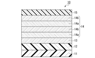
- thermoplastic resin used for the binder resin of the hard coat layer 12 examples include styrene resin, (meth) acrylic resin, vinyl acetate resin, vinyl ether resin, halogen-containing resin, alicyclic olefin resin, and polycarbonate resin. Examples thereof include resins, polyester resins, polyamide resins, cellulose derivatives, silicone resins and rubbers or elastomers.
- the thermoplastic resin is preferably amorphous and soluble in an organic solvent (particularly a common solvent capable of dissolving a plurality of polymers and curable compounds).
- a compound composed of a fluorine-modified organic group and a reactive silyl group for example, alkoxysilane
- examples of commercially available products include Optool DSX (manufactured by Daikin Corporation) and KY-100 series (manufactured by Shin-Etsu Chemical Co., Ltd.).
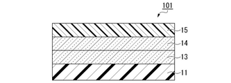
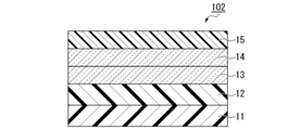
- the antifouling layer 15 differs depending on the use and configuration of the optical laminate.
- the average length RSm of the elements of the antifouling layer 15 is preferably 55 nm or more, for example. It is more preferably 90 nm or less.
- the average length RSm of the elements of the antifouling layer referred to here reflects the average length of the elements of the optical functional layer 14.
- the average length RSm of the elements of the antifouling layer 15 referred to here is a value before the scratch resistance test is performed.
- L0 * , a0 * , and b0 * are the values before the scratch resistance test
- L1 * , a1 * , and b1 * are the values after the scratch resistance test.
- the transparent base material 11 having the adhesion layer 13 and the optical functional layer 14 formed on the hard coat layer 12 is sent out to the pretreatment device 2B by the rotation of the film forming roll 25 and the guide roll 22.
- a second surface treatment step is performed as a pretreatment for the surface on which the antifouling layer 15 is formed.
- the transparent base material 11 on which the optical functional layer 14 is formed obtained by the optical functional layer forming step is continuously subjected to the second surface treatment while being maintained under reduced pressure without being exposed to the atmosphere. Perform the process.
- SR610 Polyethylene glycol diacrylate, average molecular weight of polyethylene glycol chain 600
- CN968 Hex-functional aliphatic urethane acrylate with polyester skeleton
- Irgacure 184 1-hydroxy-cyclohexyl-phenyl-ketone
- Example 9 the second surface treatment step was performed with an output of 1.0 kW, and the integrated output was 1086 W ⁇ min / m 2 .
- the film thickness of the antifouling layer was 5.0 nm.
- Example 10 was different from Example 9 in that the second surface treatment step was performed at an output of 1.5 kW, and the integrated output was 1629 W ⁇ min / m 2 .
- Example 11 was different from Example 9 in that the second surface treatment step was performed at an output of 0.5 kW, and the integrated output was 543 W ⁇ min / m 2 .
- Example 12 is different from Example 9 in that the film thickness of the antifouling layer is 4.0 nm.
- an alkoxysilane compound having a perfluoropolyether group (KY-1901, manufactured by Shin-Etsu Chemical Co., Ltd.) was used as a fluorine solvent (Florinate FC-3283: manufactured by 3M Japan Co., Ltd.) at a concentration of 0. The one diluted to 1% by mass was used. The antifouling agent was applied so that the thickness after drying was the film thickness shown in Tables 3A and 3B.
- Drop amount of each reagent 2.0 ⁇ L Measurement temperature: 25 ° C
- the contact angle after 4 seconds after dropping each reagent was measured at any 10 points on the surface of the test piece, and the average value was taken as the contact angle of oleic acid, n-hexadecane, and diiodomethane.
- X-ray Photoelectron Spectroscopy Electrode Spectroscopy for Chemical Analysis, ESCA
- PHI5000 VersaProb * eIII manufactured by ULVAC FI Co., Ltd.
- X-ray fluorescence X-ray fluorescence
Landscapes
- Chemical & Material Sciences (AREA)
- Engineering & Computer Science (AREA)
- Chemical Kinetics & Catalysis (AREA)
- Materials Engineering (AREA)
- Mechanical Engineering (AREA)
- Organic Chemistry (AREA)
- Physics & Mathematics (AREA)
- Metallurgy (AREA)
- General Physics & Mathematics (AREA)
- Optics & Photonics (AREA)
- Inorganic Chemistry (AREA)
- Health & Medical Sciences (AREA)
- Manufacturing & Machinery (AREA)
- Ophthalmology & Optometry (AREA)
- Life Sciences & Earth Sciences (AREA)
- Wood Science & Technology (AREA)
- Crystallography & Structural Chemistry (AREA)
- Surface Treatment Of Optical Elements (AREA)
- Laminated Bodies (AREA)
- Physical Vapour Deposition (AREA)
- Optical Filters (AREA)
- Electroluminescent Light Sources (AREA)
Abstract
Priority Applications (4)
| Application Number | Priority Date | Filing Date | Title |
|---|---|---|---|
| EP21866786.3A EP4212921A1 (fr) | 2020-09-10 | 2021-09-08 | Stratifié optique, article et procédé de production de stratifié optique |
| US18/044,297 US20230324584A1 (en) | 2020-09-10 | 2021-09-08 | Optical laminate, article, and production method for optical laminate |
| CN202180051438.0A CN115917366A (zh) | 2020-09-10 | 2021-09-08 | 光学层叠体、物品、光学层叠体的制造方法 |
| KR1020227044278A KR20230008227A (ko) | 2020-09-10 | 2021-09-08 | 광학 적층체, 물품, 광학 적층체의 제조 방법 |
Applications Claiming Priority (2)
| Application Number | Priority Date | Filing Date | Title |
|---|---|---|---|
| JP2020151806 | 2020-09-10 | ||
| JP2020-151806 | 2020-09-10 |
Publications (1)
| Publication Number | Publication Date |
|---|---|
| WO2022054827A1 true WO2022054827A1 (fr) | 2022-03-17 |
Family
ID=80631602
Family Applications (2)
| Application Number | Title | Priority Date | Filing Date |
|---|---|---|---|
| PCT/JP2021/032978 WO2022054827A1 (fr) | 2020-09-10 | 2021-09-08 | Stratifié optique, article et procédé de production de stratifié optique |
| PCT/JP2021/032991 WO2022054828A1 (fr) | 2020-09-10 | 2021-09-08 | Procédé de production pour stratifié optique |
Family Applications After (1)
| Application Number | Title | Priority Date | Filing Date |
|---|---|---|---|
| PCT/JP2021/032991 WO2022054828A1 (fr) | 2020-09-10 | 2021-09-08 | Procédé de production pour stratifié optique |
Country Status (7)
| Country | Link |
|---|---|
| US (2) | US20230321933A1 (fr) |
| EP (2) | EP4212921A1 (fr) |
| JP (6) | JP7204850B2 (fr) |
| KR (2) | KR20230008883A (fr) |
| CN (2) | CN116075750A (fr) |
| TW (2) | TW202225428A (fr) |
| WO (2) | WO2022054827A1 (fr) |
Families Citing this family (1)
| Publication number | Priority date | Publication date | Assignee | Title |
|---|---|---|---|---|
| JP2023167531A (ja) * | 2022-05-12 | 2023-11-24 | デクセリアルズ株式会社 | 光学積層体及び物品 |
Citations (17)
| Publication number | Priority date | Publication date | Assignee | Title |
|---|---|---|---|---|
| JPH0242970B2 (fr) | 1985-04-02 | 1990-09-26 | ||
| JP2000308846A (ja) * | 1999-04-26 | 2000-11-07 | Toppan Printing Co Ltd | 防汚層の形成方法 |
| JP2005301208A (ja) | 2004-03-17 | 2005-10-27 | Seiko Epson Corp | 防汚性光学物品の製造方法 |
| JP2006175438A (ja) | 2005-12-22 | 2006-07-06 | Toppan Printing Co Ltd | 防汚層の形成方法 |
| JP2009109850A (ja) * | 2007-10-31 | 2009-05-21 | Toppan Printing Co Ltd | 反射防止フィルム及びその製造方法並びに反射防止フィルムを用いた偏光板及びその製造方法 |
| JP2010191144A (ja) * | 2009-02-18 | 2010-09-02 | Toppan Printing Co Ltd | 反射防止フィルム |
| CN105835465A (zh) * | 2015-01-13 | 2016-08-10 | 南昌欧菲光学技术有限公司 | 增透防指纹叠层及其制作方法 |
| JP2016224443A (ja) * | 2015-05-27 | 2016-12-28 | デクセリアルズ株式会社 | 積層薄膜、及び積層薄膜の製造方法 |
| JP2017227898A (ja) * | 2016-06-17 | 2017-12-28 | 日東電工株式会社 | 反射防止フィルムおよびその製造方法、ならびに反射防止層付き偏光板 |
| WO2018193742A1 (fr) * | 2017-04-20 | 2018-10-25 | 信越化学工業株式会社 | Organe antireflet et son procédé de fabrication |
| WO2019064969A1 (fr) * | 2017-09-28 | 2019-04-04 | 日東電工株式会社 | Film antireflet, son procédé de production, et plaque de polarisation à couche antireflet |
| WO2019078313A1 (fr) | 2017-10-19 | 2019-04-25 | Agc株式会社 | Corps stratifié de substrat transparent et son procédé de production |
| WO2020027037A1 (fr) * | 2018-07-31 | 2020-02-06 | 日本電産株式会社 | Procédé de revêtement, composant optique et ensemble lentille |
| JP2020151806A (ja) | 2019-03-20 | 2020-09-24 | 株式会社東芝 | 研磨装置及び研磨方法 |
| WO2021106797A1 (fr) * | 2019-11-25 | 2021-06-03 | 日東電工株式会社 | Film antireflet et dispositif d'affichage d'image |
| WO2021177350A1 (fr) * | 2020-03-04 | 2021-09-10 | デクセリアルズ株式会社 | Stratifié optique, article, et procédé de production de stratifié optique |
| WO2021177348A1 (fr) * | 2020-03-04 | 2021-09-10 | デクセリアルズ株式会社 | Procédé de fabrication de stratifié optique |
Family Cites Families (1)
| Publication number | Priority date | Publication date | Assignee | Title |
|---|---|---|---|---|
| JP6542970B2 (ja) | 2018-10-10 | 2019-07-10 | デクセリアルズ株式会社 | 反射防止膜の製造方法 |
-
2021
- 2021-09-08 TW TW110133457A patent/TW202225428A/zh unknown
- 2021-09-08 KR KR1020227044279A patent/KR20230008883A/ko active IP Right Grant
- 2021-09-08 WO PCT/JP2021/032978 patent/WO2022054827A1/fr active Application Filing
- 2021-09-08 US US18/044,295 patent/US20230321933A1/en active Pending
- 2021-09-08 CN CN202180054441.8A patent/CN116075750A/zh active Pending
- 2021-09-08 KR KR1020227044278A patent/KR20230008227A/ko active IP Right Grant
- 2021-09-08 JP JP2021146049A patent/JP7204850B2/ja active Active
- 2021-09-08 EP EP21866786.3A patent/EP4212921A1/fr active Pending
- 2021-09-08 JP JP2021146047A patent/JP7204849B2/ja active Active
- 2021-09-08 WO PCT/JP2021/032991 patent/WO2022054828A1/fr active Application Filing
- 2021-09-08 EP EP21866787.1A patent/EP4212922A1/fr active Pending
- 2021-09-08 CN CN202180051438.0A patent/CN115917366A/zh active Pending
- 2021-09-08 US US18/044,297 patent/US20230324584A1/en active Pending
- 2021-09-08 TW TW110133458A patent/TW202225429A/zh unknown
-
2022
- 2022-12-28 JP JP2022211761A patent/JP7273238B2/ja active Active
- 2022-12-28 JP JP2022212380A patent/JP7273239B2/ja active Active
-
2023
- 2023-04-27 JP JP2023073343A patent/JP2023110923A/ja active Pending
- 2023-04-27 JP JP2023073426A patent/JP2023099575A/ja active Pending
Patent Citations (17)
| Publication number | Priority date | Publication date | Assignee | Title |
|---|---|---|---|---|
| JPH0242970B2 (fr) | 1985-04-02 | 1990-09-26 | ||
| JP2000308846A (ja) * | 1999-04-26 | 2000-11-07 | Toppan Printing Co Ltd | 防汚層の形成方法 |
| JP2005301208A (ja) | 2004-03-17 | 2005-10-27 | Seiko Epson Corp | 防汚性光学物品の製造方法 |
| JP2006175438A (ja) | 2005-12-22 | 2006-07-06 | Toppan Printing Co Ltd | 防汚層の形成方法 |
| JP2009109850A (ja) * | 2007-10-31 | 2009-05-21 | Toppan Printing Co Ltd | 反射防止フィルム及びその製造方法並びに反射防止フィルムを用いた偏光板及びその製造方法 |
| JP2010191144A (ja) * | 2009-02-18 | 2010-09-02 | Toppan Printing Co Ltd | 反射防止フィルム |
| CN105835465A (zh) * | 2015-01-13 | 2016-08-10 | 南昌欧菲光学技术有限公司 | 增透防指纹叠层及其制作方法 |
| JP2016224443A (ja) * | 2015-05-27 | 2016-12-28 | デクセリアルズ株式会社 | 積層薄膜、及び積層薄膜の製造方法 |
| JP2017227898A (ja) * | 2016-06-17 | 2017-12-28 | 日東電工株式会社 | 反射防止フィルムおよびその製造方法、ならびに反射防止層付き偏光板 |
| WO2018193742A1 (fr) * | 2017-04-20 | 2018-10-25 | 信越化学工業株式会社 | Organe antireflet et son procédé de fabrication |
| WO2019064969A1 (fr) * | 2017-09-28 | 2019-04-04 | 日東電工株式会社 | Film antireflet, son procédé de production, et plaque de polarisation à couche antireflet |
| WO2019078313A1 (fr) | 2017-10-19 | 2019-04-25 | Agc株式会社 | Corps stratifié de substrat transparent et son procédé de production |
| WO2020027037A1 (fr) * | 2018-07-31 | 2020-02-06 | 日本電産株式会社 | Procédé de revêtement, composant optique et ensemble lentille |
| JP2020151806A (ja) | 2019-03-20 | 2020-09-24 | 株式会社東芝 | 研磨装置及び研磨方法 |
| WO2021106797A1 (fr) * | 2019-11-25 | 2021-06-03 | 日東電工株式会社 | Film antireflet et dispositif d'affichage d'image |
| WO2021177350A1 (fr) * | 2020-03-04 | 2021-09-10 | デクセリアルズ株式会社 | Stratifié optique, article, et procédé de production de stratifié optique |
| WO2021177348A1 (fr) * | 2020-03-04 | 2021-09-10 | デクセリアルズ株式会社 | Procédé de fabrication de stratifié optique |
Also Published As
| Publication number | Publication date |
|---|---|
| JP7273239B2 (ja) | 2023-05-12 |
| JP7273238B2 (ja) | 2023-05-12 |
| US20230324584A1 (en) | 2023-10-12 |
| CN116075750A (zh) | 2023-05-05 |
| WO2022054828A1 (fr) | 2022-03-17 |
| JP7204850B2 (ja) | 2023-01-16 |
| JP2022046446A (ja) | 2022-03-23 |
| JP2023054799A (ja) | 2023-04-14 |
| JP7204849B2 (ja) | 2023-01-16 |
| TW202225428A (zh) | 2022-07-01 |
| CN115917366A (zh) | 2023-04-04 |
| JP2023099575A (ja) | 2023-07-13 |
| KR20230008227A (ko) | 2023-01-13 |
| KR20230008883A (ko) | 2023-01-16 |
| JP2022046445A (ja) | 2022-03-23 |
| US20230321933A1 (en) | 2023-10-12 |
| EP4212922A1 (fr) | 2023-07-19 |
| JP2023040132A (ja) | 2023-03-22 |
| JP2023110923A (ja) | 2023-08-09 |
| EP4212921A1 (fr) | 2023-07-19 |
| TW202225429A (zh) | 2022-07-01 |
Similar Documents
| Publication | Publication Date | Title |
|---|---|---|
| WO2021177350A1 (fr) | Stratifié optique, article, et procédé de production de stratifié optique | |
| JP7101297B2 (ja) | 光学積層体、物品、光学積層体の製造方法 | |
| JP7147095B2 (ja) | 光学積層体の製造方法 | |
| WO2022014701A1 (fr) | Procédé de production de corps optique multicouche | |
| JP7273239B2 (ja) | 光学積層体、物品、光学積層体の製造方法 | |
| JP7089609B2 (ja) | 光学積層体、物品、光学積層体の製造方法 | |
| WO2022014696A1 (fr) | Stratifié optique, article et procédé de production de stratifié optique | |
| JP7089610B2 (ja) | 光学積層体の製造方法 | |
| JP7303954B2 (ja) | 光学積層体の製造方法 | |
| JP7248830B2 (ja) | 光学積層体の製造方法 | |
| TW202216458A (zh) | 光學積層體之製造方法 |
Legal Events
| Date | Code | Title | Description |
|---|---|---|---|
| 121 | Ep: the epo has been informed by wipo that ep was designated in this application |
Ref document number: 21866786 Country of ref document: EP Kind code of ref document: A1 |
|
| ENP | Entry into the national phase |
Ref document number: 20227044278 Country of ref document: KR Kind code of ref document: A |
|
| WWE | Wipo information: entry into national phase |
Ref document number: 202317015235 Country of ref document: IN |
|
| NENP | Non-entry into the national phase |
Ref country code: DE |
|
| ENP | Entry into the national phase |
Ref document number: 2021866786 Country of ref document: EP Effective date: 20230411 |