WO2018143050A1 - 半導体装置 - Google Patents
半導体装置 Download PDFInfo
- Publication number
- WO2018143050A1 WO2018143050A1 PCT/JP2018/002276 JP2018002276W WO2018143050A1 WO 2018143050 A1 WO2018143050 A1 WO 2018143050A1 JP 2018002276 W JP2018002276 W JP 2018002276W WO 2018143050 A1 WO2018143050 A1 WO 2018143050A1
- Authority
- WO
- WIPO (PCT)
- Prior art keywords
- distance
- layer
- outer peripheral
- semiconductor substrate
- electrode
- Prior art date
- Legal status (The legal status is an assumption and is not a legal conclusion. Google has not performed a legal analysis and makes no representation as to the accuracy of the status listed.)
- Ceased
Links
Images


Classifications
-
- H—ELECTRICITY
- H10—SEMICONDUCTOR DEVICES; ELECTRIC SOLID-STATE DEVICES NOT OTHERWISE PROVIDED FOR
- H10D—INORGANIC ELECTRIC SEMICONDUCTOR DEVICES
- H10D62/00—Semiconductor bodies, or regions thereof, of devices having potential barriers
- H10D62/10—Shapes, relative sizes or dispositions of the regions of the semiconductor bodies; Shapes of the semiconductor bodies
- H10D62/102—Constructional design considerations for preventing surface leakage or controlling electric field concentration
- H10D62/103—Constructional design considerations for preventing surface leakage or controlling electric field concentration for increasing or controlling the breakdown voltage of reverse-biased devices
- H10D62/105—Constructional design considerations for preventing surface leakage or controlling electric field concentration for increasing or controlling the breakdown voltage of reverse-biased devices by having particular doping profiles, shapes or arrangements of PN junctions; by having supplementary regions, e.g. junction termination extension [JTE]
- H10D62/106—Constructional design considerations for preventing surface leakage or controlling electric field concentration for increasing or controlling the breakdown voltage of reverse-biased devices by having particular doping profiles, shapes or arrangements of PN junctions; by having supplementary regions, e.g. junction termination extension [JTE] having supplementary regions doped oppositely to or in rectifying contact with regions of the semiconductor bodies, e.g. guard rings with PN or Schottky junctions
- H10D62/107—Buried supplementary regions, e.g. buried guard rings
-
- H—ELECTRICITY
- H10—SEMICONDUCTOR DEVICES; ELECTRIC SOLID-STATE DEVICES NOT OTHERWISE PROVIDED FOR
- H10D—INORGANIC ELECTRIC SEMICONDUCTOR DEVICES
- H10D10/00—Bipolar junction transistors [BJT]
- H10D10/40—Vertical BJTs
-
- H—ELECTRICITY
- H10—SEMICONDUCTOR DEVICES; ELECTRIC SOLID-STATE DEVICES NOT OTHERWISE PROVIDED FOR
- H10D—INORGANIC ELECTRIC SEMICONDUCTOR DEVICES
- H10D10/00—Bipolar junction transistors [BJT]
- H10D10/80—Heterojunction BJTs
- H10D10/821—Vertical heterojunction BJTs
-
- H—ELECTRICITY
- H10—SEMICONDUCTOR DEVICES; ELECTRIC SOLID-STATE DEVICES NOT OTHERWISE PROVIDED FOR
- H10D—INORGANIC ELECTRIC SEMICONDUCTOR DEVICES
- H10D12/00—Bipolar devices controlled by the field effect, e.g. insulated-gate bipolar transistors [IGBT]
- H10D12/01—Manufacture or treatment
- H10D12/031—Manufacture or treatment of IGBTs
- H10D12/032—Manufacture or treatment of IGBTs of vertical IGBTs
- H10D12/035—Etching a recess in the emitter region
-
- H—ELECTRICITY
- H10—SEMICONDUCTOR DEVICES; ELECTRIC SOLID-STATE DEVICES NOT OTHERWISE PROVIDED FOR
- H10D—INORGANIC ELECTRIC SEMICONDUCTOR DEVICES
- H10D12/00—Bipolar devices controlled by the field effect, e.g. insulated-gate bipolar transistors [IGBT]
- H10D12/411—Insulated-gate bipolar transistors [IGBT]
- H10D12/441—Vertical IGBTs
- H10D12/461—Vertical IGBTs having non-planar surfaces, e.g. having trenches, recesses or pillars in the surfaces of the emitter, base or collector regions
- H10D12/481—Vertical IGBTs having non-planar surfaces, e.g. having trenches, recesses or pillars in the surfaces of the emitter, base or collector regions having gate structures on slanted surfaces, on vertical surfaces, or in grooves, e.g. trench gate IGBTs
-
- H—ELECTRICITY
- H10—SEMICONDUCTOR DEVICES; ELECTRIC SOLID-STATE DEVICES NOT OTHERWISE PROVIDED FOR
- H10D—INORGANIC ELECTRIC SEMICONDUCTOR DEVICES
- H10D62/00—Semiconductor bodies, or regions thereof, of devices having potential barriers
- H10D62/10—Shapes, relative sizes or dispositions of the regions of the semiconductor bodies; Shapes of the semiconductor bodies
- H10D62/102—Constructional design considerations for preventing surface leakage or controlling electric field concentration
- H10D62/103—Constructional design considerations for preventing surface leakage or controlling electric field concentration for increasing or controlling the breakdown voltage of reverse-biased devices
- H10D62/105—Constructional design considerations for preventing surface leakage or controlling electric field concentration for increasing or controlling the breakdown voltage of reverse-biased devices by having particular doping profiles, shapes or arrangements of PN junctions; by having supplementary regions, e.g. junction termination extension [JTE]
- H10D62/106—Constructional design considerations for preventing surface leakage or controlling electric field concentration for increasing or controlling the breakdown voltage of reverse-biased devices by having particular doping profiles, shapes or arrangements of PN junctions; by having supplementary regions, e.g. junction termination extension [JTE] having supplementary regions doped oppositely to or in rectifying contact with regions of the semiconductor bodies, e.g. guard rings with PN or Schottky junctions
-
- H—ELECTRICITY
- H10—SEMICONDUCTOR DEVICES; ELECTRIC SOLID-STATE DEVICES NOT OTHERWISE PROVIDED FOR
- H10D—INORGANIC ELECTRIC SEMICONDUCTOR DEVICES
- H10D62/00—Semiconductor bodies, or regions thereof, of devices having potential barriers
- H10D62/10—Shapes, relative sizes or dispositions of the regions of the semiconductor bodies; Shapes of the semiconductor bodies
- H10D62/13—Semiconductor regions connected to electrodes carrying current to be rectified, amplified or switched, e.g. source or drain regions
- H10D62/137—Collector regions of BJTs
-
- H—ELECTRICITY
- H10—SEMICONDUCTOR DEVICES; ELECTRIC SOLID-STATE DEVICES NOT OTHERWISE PROVIDED FOR
- H10D—INORGANIC ELECTRIC SEMICONDUCTOR DEVICES
- H10D62/00—Semiconductor bodies, or regions thereof, of devices having potential barriers
- H10D62/10—Shapes, relative sizes or dispositions of the regions of the semiconductor bodies; Shapes of the semiconductor bodies
- H10D62/13—Semiconductor regions connected to electrodes carrying current to be rectified, amplified or switched, e.g. source or drain regions
- H10D62/141—Anode or cathode regions of thyristors; Collector or emitter regions of gated bipolar-mode devices, e.g. of IGBTs
- H10D62/142—Anode regions of thyristors or collector regions of gated bipolar-mode devices
-
- H—ELECTRICITY
- H10—SEMICONDUCTOR DEVICES; ELECTRIC SOLID-STATE DEVICES NOT OTHERWISE PROVIDED FOR
- H10D—INORGANIC ELECTRIC SEMICONDUCTOR DEVICES
- H10D62/00—Semiconductor bodies, or regions thereof, of devices having potential barriers
- H10D62/10—Shapes, relative sizes or dispositions of the regions of the semiconductor bodies; Shapes of the semiconductor bodies
- H10D62/17—Semiconductor regions connected to electrodes not carrying current to be rectified, amplified or switched, e.g. channel regions
- H10D62/393—Body regions of DMOS transistors or IGBTs
-
- H—ELECTRICITY
- H10—SEMICONDUCTOR DEVICES; ELECTRIC SOLID-STATE DEVICES NOT OTHERWISE PROVIDED FOR
- H10D—INORGANIC ELECTRIC SEMICONDUCTOR DEVICES
- H10D62/00—Semiconductor bodies, or regions thereof, of devices having potential barriers
- H10D62/60—Impurity distributions or concentrations
-
- H—ELECTRICITY
- H10—SEMICONDUCTOR DEVICES; ELECTRIC SOLID-STATE DEVICES NOT OTHERWISE PROVIDED FOR
- H10D—INORGANIC ELECTRIC SEMICONDUCTOR DEVICES
- H10D64/00—Electrodes of devices having potential barriers
- H10D64/111—Field plates
- H10D64/112—Field plates comprising multiple field plate segments
-
- H—ELECTRICITY
- H10—SEMICONDUCTOR DEVICES; ELECTRIC SOLID-STATE DEVICES NOT OTHERWISE PROVIDED FOR
- H10D—INORGANIC ELECTRIC SEMICONDUCTOR DEVICES
- H10D64/00—Electrodes of devices having potential barriers
- H10D64/20—Electrodes characterised by their shapes, relative sizes or dispositions
- H10D64/27—Electrodes not carrying the current to be rectified, amplified, oscillated or switched, e.g. gates
- H10D64/311—Gate electrodes for field-effect devices
- H10D64/411—Gate electrodes for field-effect devices for FETs
- H10D64/511—Gate electrodes for field-effect devices for FETs for IGFETs
- H10D64/517—Gate electrodes for field-effect devices for FETs for IGFETs characterised by the conducting layers
- H10D64/518—Gate electrodes for field-effect devices for FETs for IGFETs characterised by the conducting layers characterised by their lengths or sectional shapes
-
- H—ELECTRICITY
- H10—SEMICONDUCTOR DEVICES; ELECTRIC SOLID-STATE DEVICES NOT OTHERWISE PROVIDED FOR
- H10D—INORGANIC ELECTRIC SEMICONDUCTOR DEVICES
- H10D64/00—Electrodes of devices having potential barriers
- H10D64/20—Electrodes characterised by their shapes, relative sizes or dispositions
- H10D64/27—Electrodes not carrying the current to be rectified, amplified, oscillated or switched, e.g. gates
- H10D64/311—Gate electrodes for field-effect devices
- H10D64/411—Gate electrodes for field-effect devices for FETs
- H10D64/511—Gate electrodes for field-effect devices for FETs for IGFETs
- H10D64/517—Gate electrodes for field-effect devices for FETs for IGFETs characterised by the conducting layers
- H10D64/519—Gate electrodes for field-effect devices for FETs for IGFETs characterised by the conducting layers characterised by their top-view geometrical layouts
-
- H—ELECTRICITY
- H10—SEMICONDUCTOR DEVICES; ELECTRIC SOLID-STATE DEVICES NOT OTHERWISE PROVIDED FOR
- H10D—INORGANIC ELECTRIC SEMICONDUCTOR DEVICES
- H10D84/00—Integrated devices formed in or on semiconductor substrates that comprise only semiconducting layers, e.g. on Si wafers or on GaAs-on-Si wafers
- H10D84/60—Integrated devices formed in or on semiconductor substrates that comprise only semiconducting layers, e.g. on Si wafers or on GaAs-on-Si wafers characterised by the integration of at least one component covered by groups H10D10/00 or H10D18/00, e.g. integration of BJTs
- H10D84/641—Combinations of only vertical BJTs
-
- H—ELECTRICITY
- H10—SEMICONDUCTOR DEVICES; ELECTRIC SOLID-STATE DEVICES NOT OTHERWISE PROVIDED FOR
- H10D—INORGANIC ELECTRIC SEMICONDUCTOR DEVICES
- H10D64/00—Electrodes of devices having potential barriers
- H10D64/20—Electrodes characterised by their shapes, relative sizes or dispositions
- H10D64/27—Electrodes not carrying the current to be rectified, amplified, oscillated or switched, e.g. gates
- H10D64/311—Gate electrodes for field-effect devices
- H10D64/411—Gate electrodes for field-effect devices for FETs
- H10D64/511—Gate electrodes for field-effect devices for FETs for IGFETs
- H10D64/512—Disposition of the gate electrodes, e.g. buried gates
- H10D64/513—Disposition of the gate electrodes, e.g. buried gates within recesses in the substrate, e.g. trench gates, groove gates or buried gates
Definitions
- the present invention relates to a semiconductor device having an element part in which an insulated gate bipolar transistor (hereinafter simply referred to as IGBT) element is formed and an outer peripheral part surrounding the element part.
- IGBT insulated gate bipolar transistor
- this semiconductor device includes a semiconductor substrate that has one surface and another surface opposite to the one surface and forms a drift layer.
- a P-type base layer is formed on the drift layer, and an N + -type emitter region is formed on the surface layer portion of the base layer.
- a gate electrode is formed so as to be in contact with the base layer through the gate insulating film.
- a collector layer is formed on the side of the drift layer opposite to the base layer. The collector layer is formed from the element portion to the outer peripheral portion.
- An upper electrode is formed on one side of the semiconductor substrate so as to be electrically connected to the base layer and the emitter region, and is connected to a collector layer on the other side of the semiconductor substrate.
- a lower electrode is formed.
- a plurality of P + type deep layers are formed on one surface side of the semiconductor substrate so as to form a multiple ring structure.
- the plurality of deep layers are formed deeper than the base layer so that the electric field concentration in the element portion is suppressed.
- an inversion layer that is, a channel region
- electrons are supplied from the emitter region to the drift layer via the inversion layer, and holes are supplied from the collector layer to the drift layer, and the resistance value of the drift layer is lowered by conductivity modulation, and current flows.
- the semiconductor device since the deep layer deeper than the base layer is formed at the outer peripheral portion, the substantial thickness of the drift layer is thinner than the element portion at the outer peripheral portion, and the breakdown voltage decreases. .
- the collector layer is also formed on the outer peripheral portion, and holes are also supplied to the drift layer from the collector layer formed on the outer peripheral portion. For this reason, in the semiconductor device, when the current is interrupted from the state where the current flows, breakdown is likely to occur at the outer peripheral portion. Since the semiconductor device is less likely to sweep out current at the outer peripheral portion than at the element portion, there is a high possibility that the semiconductor device will be destroyed if breakdown occurs at the outer peripheral portion.
- An object of the present disclosure is to provide a semiconductor device having a deep layer formed deeper than the base layer in the outer peripheral portion and capable of suppressing the occurrence of breakdown in the outer peripheral portion.
- a semiconductor device having an element portion and an outer peripheral portion surrounding the element portion has one surface and another surface opposite to the one surface, and constitutes a first conductivity type drift layer.
- a semiconductor substrate, a second conductivity type base layer formed on one surface side of the semiconductor substrate on the drift layer in the element portion, and reaches the drift layer through the base layer, along the surface direction of the semiconductor substrate A gate insulating film formed on each of the wall surfaces of the plurality of trenches extended, a gate electrode formed on the gate insulating film, and a first conductivity type formed on a surface layer portion of the base layer and in contact with the trench
- first carriers are injected from the first electrode into the drift layer through the emitter region, and drift from the second electrode through the collector layer.
- a current flows between the first electrode and the second electrode by injecting the second carrier into the layer, and on one surface of the semiconductor substrate, the position closest to the element portion in the deep layer is defined as a boundary position,
- the distance between the first electrode and the position on the outermost peripheral side of the emitter region where the first carriers can be injected is defined as the first distance, and the boundary position and the end of the collector layer in the plane direction of the semiconductor substrate If the distance between the first and second positions is the second distance, the carrier density in the outer peripheral portion of the first distance and the second distance is reduced based on the breakdown voltage of the outer peripheral portion reduced by the deep layer. It has been adjusted to.
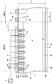
- the semiconductor device of the first embodiment will be described with reference to FIG.
- the semiconductor device according to the present embodiment includes a semiconductor substrate 10 having one surface 10a and another surface 10b opposite to the one surface 10a, and an element portion 1 on which an IGBT element is formed, and the element portion. 1 and the outer peripheral part 2 surrounding 1 are formed.
- a basic configuration of the element unit 1 will be described.
- the element section 1 has an N ⁇ type drift layer 11, and a P type base layer 12 is formed on the drift layer 11 (that is, on the one surface 10 a side of the semiconductor substrate 10).
- a plurality of trenches 13 that penetrate the base layer 12 and reach the drift layer 11 are formed, and the base layer 12 is divided by the plurality of trenches 13.
- the plurality of trenches 13 are formed at regular intervals in a stripe shape along one direction (that is, the depth direction in the drawing in FIG. 1) of the surface direction of the one surface 10a of the semiconductor substrate 10.
- the impurity concentration of the drift layer 11 is 1.0 ⁇ 10 14 cm ⁇ 3 .
- the plurality of trenches 13 are formed so that the distance between the side surfaces facing each other is constant. That is, the interval between adjacent trenches 13 is constant along the bottom side from the opening side of the trench 13.
- each gate electrode 15 is appropriately electrically connected to the gate pad 4 through the gate wiring 3 so that a predetermined gate voltage can be applied from an external gate circuit.
- N + -type emitter region 16 and a P + -type body region 17 are formed in the surface layer portion of the base layer 12.
- the emitter region 16 is configured to have a higher impurity concentration than the drift layer 11, is terminated in the base layer 12, and is in contact with the side surface of the trench 13.
- the body region 17 has a higher impurity concentration than the base layer 12 and is formed so as to terminate in the base layer 12, similarly to the emitter region 16.
- the emitter region 16 extends in a rod shape so as to be in contact with the side surface of the trench 13 along the longitudinal direction of the trench 13 in the region between the trenches 13 and terminates inside the tip of the trench 13.
- the body region 17 is sandwiched between the two emitter regions 16 and extends in a rod shape along the longitudinal direction of the trench 13 (that is, the emitter region 16). Note that the body region 17 of the present embodiment is formed deeper than the emitter region 16 with respect to the one surface 10 a of the semiconductor substrate 10.
- An interlayer insulating film 18 made of BPSG (abbreviation of Boro-phosphosilicate glass) or the like is formed on one surface 10 a of the semiconductor substrate 10.
- BPSG abbreviation of Boro-phosphosilicate glass
- An upper electrode 19 electrically connected to the emitter region 16 and the body region 17 is formed on the interlayer insulating film 18 through the first contact hole 18a.
- An N-type field stop layer (hereinafter simply referred to as an FS layer) 20 is formed on the side of the drift layer 11 opposite to the base layer 12 side (that is, the other surface 10b side of the semiconductor substrate 10).
- this FS layer 20 is not necessarily required, it is possible to improve the breakdown voltage and steady loss performance by preventing the depletion layer from spreading, and to increase the injection amount of holes injected from the other surface 10b side of the semiconductor substrate 10. Be prepared to control.
- a P-type collector layer 21 is formed on the opposite side of the drift layer 11 across the FS layer 20, and the collector layer 21 and the collector layer 21 are formed on the collector layer 21 (that is, on the other surface 10b of the semiconductor substrate 10).
- a lower electrode 22 to be electrically connected is formed.
- the outer peripheral part 2 has the same drift layer 11 as the element part 1.
- a P + -type deep layer 23 deeper than the base layer 12 is formed on the surface layer portion of the drift layer 11 so that electric field concentration of the element portion 1 is suppressed.
- the P + type deep layer 23 is formed so as to suppress the electric field concentration at the bottom of the trench 13.
- a plurality of deep layers 23 are formed, each having an annular structure surrounding the element portion 1. That is, the multiple deep layers 23 are formed so as to constitute a multiple ring structure.
- the deep layer 23 is formed so as to be deeper than the base layer 12. However, the deeper the deep layer 23, the thinner the drift layer 11 becomes and the lower the breakdown voltage. It is preferably formed so as to be deeper by about 3 ⁇ m. In the present embodiment, the deep layer 23 located closest to the element part 1 among the plurality of deep layers 23 is formed so as to be in contact with the base layer 12 formed in the element part 1. That is, it can be said that the deep layer 23 is formed continuously with the base layer 12.
- an interlayer insulating film 18 is formed on one surface 10 a of the semiconductor substrate 10, and a second contact hole 18 b that exposes the deep layer 23 is exposed in the interlayer insulating film 18. Is formed.
- An outer peripheral electrode 24 that is electrically connected to the deep layer 23 through the second contact hole 18b is formed on the interlayer insulating film 18.
- the FS layer 20 is formed on the other surface 10 b side of the semiconductor substrate 10 in the outer peripheral portion 2.
- the lower electrode 22 is formed on the FS layer 20 (that is, on the other surface 10 b of the semiconductor substrate 10).
- N + type and N ⁇ type correspond to the first conductivity type
- P type and P + type correspond to the second conductivity type
- the upper electrode 19 corresponds to the first electrode
- the lower electrode 22 corresponds to the second electrode.
- the semiconductor device when a predetermined gate voltage is applied to the gate electrode 15 from an external gate circuit while the upper electrode 19 is grounded and a positive voltage is applied to the lower electrode 22, An inversion layer (that is, a channel region) is formed at a portion in contact with the trench 13.
- An inversion layer that is, a channel region
- electrons are supplied from the emitter region 16 to the drift layer 11 through the inversion layer, and holes are supplied from the collector layer 21 to the drift layer 11.
- the resistance value of the drift layer 11 decreases due to conductivity modulation, and a current flows between the upper electrode 19 and the lower electrode 22.
- a positive voltage is applied to the upper electrode 19 and the lower electrode 22 is grounded.
- a voltage of 0 V is applied to the gate electrode 15, the upper electrode 19, the lower electrode 22,
- the current that was flowing during is interrupted.
- a state in which a current flows between the upper electrode 19 and the lower electrode 22 is that the semiconductor device is on, and a state in which the current is interrupted is that the semiconductor device is in an off state.
- electrons correspond to first carriers and holes correspond to second carriers.
- the positional relationship between the emitter region 16 and the collector layer 21 is adjusted so that the occurrence of breakdown is suppressed in the outer peripheral portion 2 when changing from the on state to the off state. That is, when the deep layer 23 deeper than the base layer 12 is formed in the outer peripheral portion 2 as described above, the substantial thickness of the drift layer 11 in the outer peripheral portion 2 is reduced, and the breakdown voltage of the outer peripheral portion 2 is likely to be reduced. For this reason, in the present embodiment, the positional relationship between the emitter region 16 and the collector layer 21 is adjusted so that breakdown does not easily occur in the outer peripheral portion 2 even if the withstand voltage decreases.
- the breakdown voltage of the outer peripheral portion 2 is reduced by forming the deep layer 23, the positional relationship between the emitter region 16 and the collector layer 21 so that the carrier density of the outer peripheral portion 2 is lowered based on the reduced breakdown voltage. Has been adjusted.
- the positional relationship between the emitter region 16 and the collector layer 21 will be specifically described.
- the position closest to the element part 1 in the deep layer 23 is defined as a boundary position K between the element part 1 and the outer peripheral part 2.
- the position on the outermost peripheral portion 2 side (hereinafter referred to as the outermost emitter position) and the boundary position A distance from K is a first distance L1.
- the distance between the position of the end portion of the collector layer 21 along the surface direction of the semiconductor substrate 10 and the boundary position K is defined as a second distance L2.
- the second distance L2 is a positive distance when the position of the end portion of the collector layer 21 along the surface direction of the semiconductor substrate 10 is located in the element portion 1, and the position of the end portion is at the outer peripheral portion 2. If it is located, the distance is negative. Further, the thickness of the semiconductor substrate 10 is set to the third distance L3. The distance between the narrowest portions of the intervals between adjacent trenches 13 is defined as a trench interval L4.
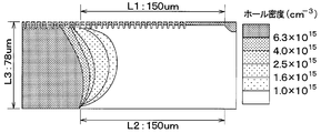
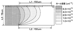
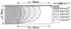
- the semiconductor device of this embodiment when a predetermined gate voltage is applied to the gate electrode 15, electrons are supplied from the emitter region 16 to the drift layer 11 and holes are generated from the collector layer 21. By being supplied to the drift layer 11, it is turned on. At this time, as shown in FIGS. 2A to 2C, it is confirmed that the hole density distribution varies depending on the trench interval d4. Then, it is confirmed that the narrower the trench interval d4, the larger the spread of the portion having a higher hole density. That is, in FIGS. 2A to 2C, the portion with the highest hole density in FIG. 2A to 2C show simulation results in which the first distance L1 is 150 ⁇ m, the second distance L2 is 150 ⁇ m, and the third distance L3 is 78 ⁇ m.
- the present inventors have examined the carrier spread on one side with respect to the plate thickness based on the trench interval L4, and obtained the results shown in FIG. That is, as shown in FIG. 3, the carrier spread A on one side with respect to the plate thickness (hereinafter simply referred to as carrier spread A) is represented by the following equation using the trench interval L4.
- Equation 1 ⁇ 0.30 ⁇ L4 + 1.53
- the carrier spread A in this embodiment is defined as follows. That is, the carrier spread A is based on the portion immediately below the outermost emitter position in the portion of the drift layer 11 closest to the one surface 10a of the semiconductor substrate 10, and the hole density is 10 times the impurity concentration of the drift layer 11 from the reference. Let us show how far the part is. In the present embodiment, since the impurity concentration of the drift layer 11 is set to 1.0 ⁇ 10 14 cm ⁇ 3 , it shows how far the portion that becomes 1.0 ⁇ 10 15 cm ⁇ 3 is separated.
- the hole density is 1.0 ⁇ 10 15 cm from the portion immediately below the outermost emitter position in the portion of the drift layer 11 closest to the one surface 10 a of the semiconductor substrate 10.
- a portion that is less than ⁇ 3 means a portion that is separated by 39 ⁇ m (that is, half the plate thickness) or more on the outer peripheral portion 2 side.
- the part where the hole density is 10 times the impurity concentration of the drift layer 11 is used as a boundary.
- the hole density exceeds 10 times the impurity concentration of the drift layer 11, the electric field strength is increased due to the positive charges of the holes. This is because the pressure drop is significantly reduced.
- the carrier spread A is a ratio to the plate thickness, the plate thickness ⁇ A is a position where the hole density is 1.0 ⁇ 10 15 cm ⁇ 3 from the reference.
- the portion of the drift layer 11 closest to the surface 10 a of the semiconductor substrate 10 is the boundary position with the base layer 12 in the case of the element portion 1. And if it is the outer peripheral part 2, it will be a boundary position with the deep layer 23. However, in the case of the outer peripheral portion 2, in the portion where the deep layer 23 is not formed, the position of the same depth as the boundary position of the portion where the deep layer 23 is formed is the most surface of the semiconductor substrate 10 in the drift layer 11. 10a side portion.
- the trench interval d4 is preferably formed at least about 100 nm apart so that the inversion layers formed along the adjacent trenches 13 are not connected to each other. Furthermore, if the trench interval d4 is too wide, the effect of accumulating holes in the drift layer 11 is remarkably reduced, so that it is preferably 8 ⁇ m or less.
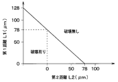
- FIG. 4 shows a simulation result when the trench interval L4 is 1.8 ⁇ m and the third distance L3 is 78 ⁇ m. That is, FIG. 4 shows a simulation result when the carrier spread A is 1. In other words, it is a simulation result when the length between the reference and the portion where the hole density is 1.0 ⁇ 10 15 cm ⁇ 3 is 78 ⁇ 1.
- Equation 2 L1 ⁇ 78 ⁇ 1-L2
- Equation 2 Equation 2
- Equation 3 L1 ⁇ L3 ⁇ A ⁇ L2
- L4 is set. For this reason, when changing from the on state to the off state, breakdown can be prevented from occurring in the outer peripheral portion 2, and the semiconductor device can be prevented from being destroyed.
- L1 L3 ⁇ ( ⁇ 0.30 ⁇ L4 + 1.53) ⁇ L2
- L1 L3 ⁇ ( ⁇ 0.30 ⁇ L4 + 1.53) ⁇ L2
- L1 L3 ⁇ ( ⁇ 0.30 ⁇ L4 + 1.53) ⁇ L2
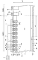
- FIG. 1 shows that the position of the end portion along the surface direction of the semiconductor substrate 10 in the collector layer 21 is located in the element portion 1.
- the position of the end portion along the surface direction of the semiconductor substrate 10 in the collector layer 21 may be located in the outer peripheral portion 2 as shown in FIG.
- the second distance L2 is a negative value.
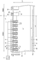
- a part of the gate electrodes 15 a among the plurality of gate electrodes 15 is connected to the gate pad 4.
- the remaining gate electrode 15 b of the plurality of gate electrodes 15 is not connected to the gate pad 4 but connected to the upper electrode 19 through the third contact hole 18 c formed in the interlayer insulating film 18. Yes. That is, the gate electrode 15b connected to the upper electrode 19 is a so-called dummy gate electrode that does not exhibit a function of forming an inversion layer in the base layer 12 when the semiconductor device is in an on state.
- the first gate electrode 15a and the second gate electrode 15b are formed on the surface of the semiconductor substrate 10. Alternatingly arranged along the direction.
- the first gate electrode 15a and the second gate electrode 15b are arranged such that the second gate electrode 15b is located on the outermost peripheral part 2 side in the arrangement direction of the first gate electrode 15a and the second gate electrode 15b. Yes.
- the emitter region 16 is formed along each trench 13 as in the first embodiment. That is, in this embodiment, the emitter region 16 is also formed on the side surface of the trench 13 in which the second gate electrode 15b is disposed.
- the first distance L1 is a distance between the outermost emitter position and the boundary position K as described above. For this reason, in the semiconductor device of this embodiment, the emitter region 16 in contact with the trench 13 in which the first gate electrode 15a is disposed, and the distance between the position on the outermost peripheral portion 2 side and the boundary position K is the first. One distance L1.
- each trench 13 has a width on the bottom side longer than a width on the opening side in the interval between the opposing side surfaces.
- the interval between the adjacent trenches 13 is such that the interval on the bottom side is shorter than the interval on the opening side. That is, in the present embodiment, the trench 13 has a so-called bowl shape.
- the trench interval L4 is the narrowest portion of the intervals between adjacent trenches 13 as described above. For this reason, in this embodiment, the trench interval L4 is a portion on the bottom side of the portion between the adjacent trenches 13.
- the manufacturing process of the emitter region 16 and the body region 17 can be simplified, and the first The same effect as that of the first embodiment can be obtained.
- the first conductivity type is N type and the second conductivity type is P type.
- the first conductivity type is P type
- the second conductivity type is N type. You can also.
- the emitter region 16 may not be formed so as to be in contact with the side surface of the trench 13 in which the second gate electrode 15b is disposed. That is, the emitter region 16 may be formed only on the side surface of the trench 13 in which the first gate electrode 15a is disposed.
- the second gate electrode 15b may not be connected to the upper electrode 19 but may be connected to a gate pad different from the gate pad 4 and maintained at a predetermined potential (for example, ground potential). It may be in a floating state without being connected to.
- the first gate electrode 15a may be located on the outermost peripheral portion 2 side in the arrangement direction of the first gate electrode 15a and the second gate electrode 15b.
- the second embodiment may be combined with the third embodiment, and the semiconductor device of the third embodiment may be configured to have the first gate electrode 15a and the second gate electrode 15b.
Landscapes
- Electrodes Of Semiconductors (AREA)
- Metal-Oxide And Bipolar Metal-Oxide Semiconductor Integrated Circuits (AREA)
Priority Applications (2)
| Application Number | Priority Date | Filing Date | Title |
|---|---|---|---|
| CN201880009680.XA CN110249431B (zh) | 2017-02-03 | 2018-01-25 | 半导体装置 |
| US16/504,858 US10748988B2 (en) | 2017-02-03 | 2019-07-08 | Semiconductor device |
Applications Claiming Priority (2)
| Application Number | Priority Date | Filing Date | Title |
|---|---|---|---|
| JP2017018672A JP6624101B2 (ja) | 2017-02-03 | 2017-02-03 | 半導体装置 |
| JP2017-018672 | 2017-02-03 |
Related Child Applications (1)
| Application Number | Title | Priority Date | Filing Date |
|---|---|---|---|
| US16/504,858 Continuation US10748988B2 (en) | 2017-02-03 | 2019-07-08 | Semiconductor device |
Publications (1)
| Publication Number | Publication Date |
|---|---|
| WO2018143050A1 true WO2018143050A1 (ja) | 2018-08-09 |
Family
ID=63039735
Family Applications (1)
| Application Number | Title | Priority Date | Filing Date |
|---|---|---|---|
| PCT/JP2018/002276 Ceased WO2018143050A1 (ja) | 2017-02-03 | 2018-01-25 | 半導体装置 |
Country Status (4)
| Country | Link |
|---|---|
| US (1) | US10748988B2 (enExample) |
| JP (1) | JP6624101B2 (enExample) |
| CN (1) | CN110249431B (enExample) |
| WO (1) | WO2018143050A1 (enExample) |
Families Citing this family (3)
| Publication number | Priority date | Publication date | Assignee | Title |
|---|---|---|---|---|
| JP7410478B2 (ja) * | 2019-07-11 | 2024-01-10 | 富士電機株式会社 | 炭化珪素半導体装置および炭化珪素半導体装置の製造方法 |
| JP7472068B2 (ja) * | 2021-03-19 | 2024-04-22 | 株式会社東芝 | 半導体装置及び半導体回路 |
| WO2022202009A1 (ja) * | 2021-03-26 | 2022-09-29 | ローム株式会社 | 半導体装置 |
Citations (2)
| Publication number | Priority date | Publication date | Assignee | Title |
|---|---|---|---|---|
| JP2010161335A (ja) * | 2008-12-10 | 2010-07-22 | Denso Corp | 半導体装置およびその製造方法 |
| JP2010177243A (ja) * | 2009-01-27 | 2010-08-12 | Denso Corp | 半導体装置 |
Family Cites Families (13)
| Publication number | Priority date | Publication date | Assignee | Title |
|---|---|---|---|---|
| JP4054155B2 (ja) | 2000-02-01 | 2008-02-27 | 三菱電機株式会社 | 半導体装置 |
| DE102004041892B4 (de) * | 2004-08-30 | 2018-08-16 | Infineon Technologies Ag | Trenchtransistor |
| JP5052091B2 (ja) * | 2006-10-20 | 2012-10-17 | 三菱電機株式会社 | 半導体装置 |
| JP5286706B2 (ja) | 2007-07-10 | 2013-09-11 | 三菱電機株式会社 | 電力用半導体装置とその製造方法 |
| JP5150195B2 (ja) | 2007-10-16 | 2013-02-20 | 株式会社東芝 | 縦型半導体装置 |
| CN101494239B (zh) * | 2009-02-27 | 2010-12-01 | 电子科技大学 | 一种高速igbt |
| JP5582102B2 (ja) | 2010-07-01 | 2014-09-03 | 株式会社デンソー | 半導体装置 |
| WO2013005304A1 (ja) | 2011-07-05 | 2013-01-10 | 三菱電機株式会社 | 半導体装置 |
| JP2014138048A (ja) | 2013-01-16 | 2014-07-28 | Sumitomo Electric Ind Ltd | 炭化珪素半導体装置 |
| JP5967065B2 (ja) * | 2013-12-17 | 2016-08-10 | トヨタ自動車株式会社 | 半導体装置 |
| JP2015153784A (ja) * | 2014-02-10 | 2015-08-24 | トヨタ自動車株式会社 | 半導体装置の製造方法及び半導体装置 |
| US9224816B2 (en) * | 2014-05-21 | 2015-12-29 | Sumitomo Electric Industries, Ltd. | Silicon carbide semiconductor device |
| JP6830767B2 (ja) * | 2016-06-14 | 2021-02-17 | 株式会社デンソー | 半導体装置 |
-
2017
- 2017-02-03 JP JP2017018672A patent/JP6624101B2/ja active Active
-
2018
- 2018-01-25 CN CN201880009680.XA patent/CN110249431B/zh active Active
- 2018-01-25 WO PCT/JP2018/002276 patent/WO2018143050A1/ja not_active Ceased
-
2019
- 2019-07-08 US US16/504,858 patent/US10748988B2/en active Active
Patent Citations (2)
| Publication number | Priority date | Publication date | Assignee | Title |
|---|---|---|---|---|
| JP2010161335A (ja) * | 2008-12-10 | 2010-07-22 | Denso Corp | 半導体装置およびその製造方法 |
| JP2010177243A (ja) * | 2009-01-27 | 2010-08-12 | Denso Corp | 半導体装置 |
Also Published As
| Publication number | Publication date |
|---|---|
| CN110249431A (zh) | 2019-09-17 |
| JP2018125490A (ja) | 2018-08-09 |
| JP6624101B2 (ja) | 2019-12-25 |
| CN110249431B (zh) | 2022-02-22 |
| US10748988B2 (en) | 2020-08-18 |
| US20190333987A1 (en) | 2019-10-31 |
Similar Documents
| Publication | Publication Date | Title |
|---|---|---|
| JP5482886B2 (ja) | 半導体装置 | |
| JP6443267B2 (ja) | 半導体装置 | |
| CN101401212B (zh) | 绝缘栅极型半导体器件及其制造方法 | |
| JP5470826B2 (ja) | 半導体装置 | |
| JPWO2018220879A1 (ja) | 半導体装置 | |
| JP6509673B2 (ja) | 半導体装置 | |
| WO2015145929A1 (ja) | 半導体装置 | |
| JP2014060362A (ja) | 半導体装置 | |
| WO2013128833A1 (ja) | 半導体装置 | |
| CN105074931B (zh) | 利用沟槽栅电极的绝缘栅双极性晶体管 | |
| JP5537359B2 (ja) | 半導体装置 | |
| JP5512455B2 (ja) | 半導体装置 | |
| NL2018610B1 (en) | Power semiconductor device and method of manufacturing power semiconductor device | |
| TW201611274A (zh) | 半導體裝置 | |
| WO2018143050A1 (ja) | 半導体装置 | |
| WO2016114131A1 (ja) | 半導体装置 | |
| US20160079350A1 (en) | Semiconductor device and manufacturing method thereof | |
| JP2019140239A (ja) | 半導体装置 | |
| JP6299658B2 (ja) | 絶縁ゲート型スイッチング素子 | |
| JP3914852B2 (ja) | ダイオード素子とトランジスタ素子 | |
| JP2018166169A (ja) | 半導体装置 | |
| JP6729478B2 (ja) | 半導体装置 | |
| JP7392613B2 (ja) | 半導体装置 | |
| JP5238866B2 (ja) | 電力用半導体装置 | |
| WO2019098122A1 (ja) | 半導体装置 |
Legal Events
| Date | Code | Title | Description |
|---|---|---|---|
| 121 | Ep: the epo has been informed by wipo that ep was designated in this application |
Ref document number: 18747592 Country of ref document: EP Kind code of ref document: A1 |
|
| NENP | Non-entry into the national phase |
Ref country code: DE |
|
| 122 | Ep: pct application non-entry in european phase |
Ref document number: 18747592 Country of ref document: EP Kind code of ref document: A1 |