WO2018143050A1 - Semiconductor device - Google Patents
Semiconductor device Download PDFInfo
- Publication number
- WO2018143050A1 WO2018143050A1 PCT/JP2018/002276 JP2018002276W WO2018143050A1 WO 2018143050 A1 WO2018143050 A1 WO 2018143050A1 JP 2018002276 W JP2018002276 W JP 2018002276W WO 2018143050 A1 WO2018143050 A1 WO 2018143050A1
- Authority
- WO
- WIPO (PCT)
- Prior art keywords
- distance
- layer
- outer peripheral
- semiconductor substrate
- electrode
- Prior art date
Links
- 239000004065 semiconductor Substances 0.000 title claims abstract description 90
- 230000002093 peripheral effect Effects 0.000 claims abstract description 58
- 239000000758 substrate Substances 0.000 claims abstract description 43
- 239000000969 carrier Substances 0.000 claims abstract description 8
- 239000010410 layer Substances 0.000 claims description 149
- 230000015556 catabolic process Effects 0.000 claims description 16
- 239000002344 surface layer Substances 0.000 claims description 7
- 230000003247 decreasing effect Effects 0.000 abstract 2
- 210000000746 body region Anatomy 0.000 description 7
- 239000012535 impurity Substances 0.000 description 7
- 239000011229 interlayer Substances 0.000 description 7
- 238000004088 simulation Methods 0.000 description 7
- 230000005684 electric field Effects 0.000 description 5
- 230000006378 damage Effects 0.000 description 3
- 230000007423 decrease Effects 0.000 description 3
- 230000000694 effects Effects 0.000 description 3
- 239000005380 borophosphosilicate glass Substances 0.000 description 2
- 238000012986 modification Methods 0.000 description 2
- 230000004048 modification Effects 0.000 description 2
- 238000009826 distribution Methods 0.000 description 1
- 238000002347 injection Methods 0.000 description 1
- 239000007924 injection Substances 0.000 description 1
- 238000004519 manufacturing process Methods 0.000 description 1
- 238000003892 spreading Methods 0.000 description 1
Images


Classifications
-
- H—ELECTRICITY
- H01—ELECTRIC ELEMENTS
- H01L—SEMICONDUCTOR DEVICES NOT COVERED BY CLASS H10
- H01L29/00—Semiconductor devices adapted for rectifying, amplifying, oscillating or switching, or capacitors or resistors with at least one potential-jump barrier or surface barrier, e.g. PN junction depletion layer or carrier concentration layer; Details of semiconductor bodies or of electrodes thereof ; Multistep manufacturing processes therefor
- H01L29/02—Semiconductor bodies ; Multistep manufacturing processes therefor
- H01L29/06—Semiconductor bodies ; Multistep manufacturing processes therefor characterised by their shape; characterised by the shapes, relative sizes, or dispositions of the semiconductor regions ; characterised by the concentration or distribution of impurities within semiconductor regions
- H01L29/0603—Semiconductor bodies ; Multistep manufacturing processes therefor characterised by their shape; characterised by the shapes, relative sizes, or dispositions of the semiconductor regions ; characterised by the concentration or distribution of impurities within semiconductor regions characterised by particular constructional design considerations, e.g. for preventing surface leakage, for controlling electric field concentration or for internal isolations regions
- H01L29/0607—Semiconductor bodies ; Multistep manufacturing processes therefor characterised by their shape; characterised by the shapes, relative sizes, or dispositions of the semiconductor regions ; characterised by the concentration or distribution of impurities within semiconductor regions characterised by particular constructional design considerations, e.g. for preventing surface leakage, for controlling electric field concentration or for internal isolations regions for preventing surface leakage or controlling electric field concentration
- H01L29/0611—Semiconductor bodies ; Multistep manufacturing processes therefor characterised by their shape; characterised by the shapes, relative sizes, or dispositions of the semiconductor regions ; characterised by the concentration or distribution of impurities within semiconductor regions characterised by particular constructional design considerations, e.g. for preventing surface leakage, for controlling electric field concentration or for internal isolations regions for preventing surface leakage or controlling electric field concentration for increasing or controlling the breakdown voltage of reverse biased devices
- H01L29/0615—Semiconductor bodies ; Multistep manufacturing processes therefor characterised by their shape; characterised by the shapes, relative sizes, or dispositions of the semiconductor regions ; characterised by the concentration or distribution of impurities within semiconductor regions characterised by particular constructional design considerations, e.g. for preventing surface leakage, for controlling electric field concentration or for internal isolations regions for preventing surface leakage or controlling electric field concentration for increasing or controlling the breakdown voltage of reverse biased devices by the doping profile or the shape or the arrangement of the PN junction, or with supplementary regions, e.g. junction termination extension [JTE]
- H01L29/0619—Semiconductor bodies ; Multistep manufacturing processes therefor characterised by their shape; characterised by the shapes, relative sizes, or dispositions of the semiconductor regions ; characterised by the concentration or distribution of impurities within semiconductor regions characterised by particular constructional design considerations, e.g. for preventing surface leakage, for controlling electric field concentration or for internal isolations regions for preventing surface leakage or controlling electric field concentration for increasing or controlling the breakdown voltage of reverse biased devices by the doping profile or the shape or the arrangement of the PN junction, or with supplementary regions, e.g. junction termination extension [JTE] with a supplementary region doped oppositely to or in rectifying contact with the semiconductor containing or contacting region, e.g. guard rings with PN or Schottky junction
- H01L29/0623—Buried supplementary region, e.g. buried guard ring
-
- H—ELECTRICITY
- H01—ELECTRIC ELEMENTS
- H01L—SEMICONDUCTOR DEVICES NOT COVERED BY CLASS H10
- H01L29/00—Semiconductor devices adapted for rectifying, amplifying, oscillating or switching, or capacitors or resistors with at least one potential-jump barrier or surface barrier, e.g. PN junction depletion layer or carrier concentration layer; Details of semiconductor bodies or of electrodes thereof ; Multistep manufacturing processes therefor
- H01L29/02—Semiconductor bodies ; Multistep manufacturing processes therefor
- H01L29/06—Semiconductor bodies ; Multistep manufacturing processes therefor characterised by their shape; characterised by the shapes, relative sizes, or dispositions of the semiconductor regions ; characterised by the concentration or distribution of impurities within semiconductor regions
- H01L29/08—Semiconductor bodies ; Multistep manufacturing processes therefor characterised by their shape; characterised by the shapes, relative sizes, or dispositions of the semiconductor regions ; characterised by the concentration or distribution of impurities within semiconductor regions with semiconductor regions connected to an electrode carrying current to be rectified, amplified or switched and such electrode being part of a semiconductor device which comprises three or more electrodes
- H01L29/083—Anode or cathode regions of thyristors or gated bipolar-mode devices
- H01L29/0834—Anode regions of thyristors or gated bipolar-mode devices, e.g. supplementary regions surrounding anode regions
-
- H—ELECTRICITY
- H01—ELECTRIC ELEMENTS
- H01L—SEMICONDUCTOR DEVICES NOT COVERED BY CLASS H10
- H01L27/00—Devices consisting of a plurality of semiconductor or other solid-state components formed in or on a common substrate
- H01L27/02—Devices consisting of a plurality of semiconductor or other solid-state components formed in or on a common substrate including semiconductor components specially adapted for rectifying, oscillating, amplifying or switching and having at least one potential-jump barrier or surface barrier; including integrated passive circuit elements with at least one potential-jump barrier or surface barrier
- H01L27/04—Devices consisting of a plurality of semiconductor or other solid-state components formed in or on a common substrate including semiconductor components specially adapted for rectifying, oscillating, amplifying or switching and having at least one potential-jump barrier or surface barrier; including integrated passive circuit elements with at least one potential-jump barrier or surface barrier the substrate being a semiconductor body
- H01L27/08—Devices consisting of a plurality of semiconductor or other solid-state components formed in or on a common substrate including semiconductor components specially adapted for rectifying, oscillating, amplifying or switching and having at least one potential-jump barrier or surface barrier; including integrated passive circuit elements with at least one potential-jump barrier or surface barrier the substrate being a semiconductor body including only semiconductor components of a single kind
- H01L27/082—Devices consisting of a plurality of semiconductor or other solid-state components formed in or on a common substrate including semiconductor components specially adapted for rectifying, oscillating, amplifying or switching and having at least one potential-jump barrier or surface barrier; including integrated passive circuit elements with at least one potential-jump barrier or surface barrier the substrate being a semiconductor body including only semiconductor components of a single kind including bipolar components only
- H01L27/0823—Devices consisting of a plurality of semiconductor or other solid-state components formed in or on a common substrate including semiconductor components specially adapted for rectifying, oscillating, amplifying or switching and having at least one potential-jump barrier or surface barrier; including integrated passive circuit elements with at least one potential-jump barrier or surface barrier the substrate being a semiconductor body including only semiconductor components of a single kind including bipolar components only including vertical bipolar transistors only
-
- H—ELECTRICITY
- H01—ELECTRIC ELEMENTS
- H01L—SEMICONDUCTOR DEVICES NOT COVERED BY CLASS H10
- H01L29/00—Semiconductor devices adapted for rectifying, amplifying, oscillating or switching, or capacitors or resistors with at least one potential-jump barrier or surface barrier, e.g. PN junction depletion layer or carrier concentration layer; Details of semiconductor bodies or of electrodes thereof ; Multistep manufacturing processes therefor
- H01L29/02—Semiconductor bodies ; Multistep manufacturing processes therefor
- H01L29/06—Semiconductor bodies ; Multistep manufacturing processes therefor characterised by their shape; characterised by the shapes, relative sizes, or dispositions of the semiconductor regions ; characterised by the concentration or distribution of impurities within semiconductor regions
- H01L29/0603—Semiconductor bodies ; Multistep manufacturing processes therefor characterised by their shape; characterised by the shapes, relative sizes, or dispositions of the semiconductor regions ; characterised by the concentration or distribution of impurities within semiconductor regions characterised by particular constructional design considerations, e.g. for preventing surface leakage, for controlling electric field concentration or for internal isolations regions
- H01L29/0607—Semiconductor bodies ; Multistep manufacturing processes therefor characterised by their shape; characterised by the shapes, relative sizes, or dispositions of the semiconductor regions ; characterised by the concentration or distribution of impurities within semiconductor regions characterised by particular constructional design considerations, e.g. for preventing surface leakage, for controlling electric field concentration or for internal isolations regions for preventing surface leakage or controlling electric field concentration
- H01L29/0611—Semiconductor bodies ; Multistep manufacturing processes therefor characterised by their shape; characterised by the shapes, relative sizes, or dispositions of the semiconductor regions ; characterised by the concentration or distribution of impurities within semiconductor regions characterised by particular constructional design considerations, e.g. for preventing surface leakage, for controlling electric field concentration or for internal isolations regions for preventing surface leakage or controlling electric field concentration for increasing or controlling the breakdown voltage of reverse biased devices
- H01L29/0615—Semiconductor bodies ; Multistep manufacturing processes therefor characterised by their shape; characterised by the shapes, relative sizes, or dispositions of the semiconductor regions ; characterised by the concentration or distribution of impurities within semiconductor regions characterised by particular constructional design considerations, e.g. for preventing surface leakage, for controlling electric field concentration or for internal isolations regions for preventing surface leakage or controlling electric field concentration for increasing or controlling the breakdown voltage of reverse biased devices by the doping profile or the shape or the arrangement of the PN junction, or with supplementary regions, e.g. junction termination extension [JTE]
- H01L29/0619—Semiconductor bodies ; Multistep manufacturing processes therefor characterised by their shape; characterised by the shapes, relative sizes, or dispositions of the semiconductor regions ; characterised by the concentration or distribution of impurities within semiconductor regions characterised by particular constructional design considerations, e.g. for preventing surface leakage, for controlling electric field concentration or for internal isolations regions for preventing surface leakage or controlling electric field concentration for increasing or controlling the breakdown voltage of reverse biased devices by the doping profile or the shape or the arrangement of the PN junction, or with supplementary regions, e.g. junction termination extension [JTE] with a supplementary region doped oppositely to or in rectifying contact with the semiconductor containing or contacting region, e.g. guard rings with PN or Schottky junction
-
- H—ELECTRICITY
- H01—ELECTRIC ELEMENTS
- H01L—SEMICONDUCTOR DEVICES NOT COVERED BY CLASS H10
- H01L29/00—Semiconductor devices adapted for rectifying, amplifying, oscillating or switching, or capacitors or resistors with at least one potential-jump barrier or surface barrier, e.g. PN junction depletion layer or carrier concentration layer; Details of semiconductor bodies or of electrodes thereof ; Multistep manufacturing processes therefor
- H01L29/02—Semiconductor bodies ; Multistep manufacturing processes therefor
- H01L29/06—Semiconductor bodies ; Multistep manufacturing processes therefor characterised by their shape; characterised by the shapes, relative sizes, or dispositions of the semiconductor regions ; characterised by the concentration or distribution of impurities within semiconductor regions
- H01L29/08—Semiconductor bodies ; Multistep manufacturing processes therefor characterised by their shape; characterised by the shapes, relative sizes, or dispositions of the semiconductor regions ; characterised by the concentration or distribution of impurities within semiconductor regions with semiconductor regions connected to an electrode carrying current to be rectified, amplified or switched and such electrode being part of a semiconductor device which comprises three or more electrodes
- H01L29/0821—Collector regions of bipolar transistors
-
- H—ELECTRICITY
- H01—ELECTRIC ELEMENTS
- H01L—SEMICONDUCTOR DEVICES NOT COVERED BY CLASS H10
- H01L29/00—Semiconductor devices adapted for rectifying, amplifying, oscillating or switching, or capacitors or resistors with at least one potential-jump barrier or surface barrier, e.g. PN junction depletion layer or carrier concentration layer; Details of semiconductor bodies or of electrodes thereof ; Multistep manufacturing processes therefor
- H01L29/02—Semiconductor bodies ; Multistep manufacturing processes therefor
- H01L29/06—Semiconductor bodies ; Multistep manufacturing processes therefor characterised by their shape; characterised by the shapes, relative sizes, or dispositions of the semiconductor regions ; characterised by the concentration or distribution of impurities within semiconductor regions
- H01L29/10—Semiconductor bodies ; Multistep manufacturing processes therefor characterised by their shape; characterised by the shapes, relative sizes, or dispositions of the semiconductor regions ; characterised by the concentration or distribution of impurities within semiconductor regions with semiconductor regions connected to an electrode not carrying current to be rectified, amplified or switched and such electrode being part of a semiconductor device which comprises three or more electrodes
- H01L29/1095—Body region, i.e. base region, of DMOS transistors or IGBTs
-
- H—ELECTRICITY
- H01—ELECTRIC ELEMENTS
- H01L—SEMICONDUCTOR DEVICES NOT COVERED BY CLASS H10
- H01L29/00—Semiconductor devices adapted for rectifying, amplifying, oscillating or switching, or capacitors or resistors with at least one potential-jump barrier or surface barrier, e.g. PN junction depletion layer or carrier concentration layer; Details of semiconductor bodies or of electrodes thereof ; Multistep manufacturing processes therefor
- H01L29/02—Semiconductor bodies ; Multistep manufacturing processes therefor
- H01L29/36—Semiconductor bodies ; Multistep manufacturing processes therefor characterised by the concentration or distribution of impurities in the bulk material
-
- H—ELECTRICITY
- H01—ELECTRIC ELEMENTS
- H01L—SEMICONDUCTOR DEVICES NOT COVERED BY CLASS H10
- H01L29/00—Semiconductor devices adapted for rectifying, amplifying, oscillating or switching, or capacitors or resistors with at least one potential-jump barrier or surface barrier, e.g. PN junction depletion layer or carrier concentration layer; Details of semiconductor bodies or of electrodes thereof ; Multistep manufacturing processes therefor
- H01L29/40—Electrodes ; Multistep manufacturing processes therefor
- H01L29/402—Field plates
- H01L29/404—Multiple field plate structures
-
- H—ELECTRICITY
- H01—ELECTRIC ELEMENTS
- H01L—SEMICONDUCTOR DEVICES NOT COVERED BY CLASS H10
- H01L29/00—Semiconductor devices adapted for rectifying, amplifying, oscillating or switching, or capacitors or resistors with at least one potential-jump barrier or surface barrier, e.g. PN junction depletion layer or carrier concentration layer; Details of semiconductor bodies or of electrodes thereof ; Multistep manufacturing processes therefor
- H01L29/40—Electrodes ; Multistep manufacturing processes therefor
- H01L29/41—Electrodes ; Multistep manufacturing processes therefor characterised by their shape, relative sizes or dispositions
- H01L29/423—Electrodes ; Multistep manufacturing processes therefor characterised by their shape, relative sizes or dispositions not carrying the current to be rectified, amplified or switched
- H01L29/42312—Gate electrodes for field effect devices
- H01L29/42316—Gate electrodes for field effect devices for field-effect transistors
- H01L29/4232—Gate electrodes for field effect devices for field-effect transistors with insulated gate
- H01L29/42372—Gate electrodes for field effect devices for field-effect transistors with insulated gate characterised by the conducting layer, e.g. the length, the sectional shape or the lay-out
- H01L29/42376—Gate electrodes for field effect devices for field-effect transistors with insulated gate characterised by the conducting layer, e.g. the length, the sectional shape or the lay-out characterised by the length or the sectional shape
-
- H—ELECTRICITY
- H01—ELECTRIC ELEMENTS
- H01L—SEMICONDUCTOR DEVICES NOT COVERED BY CLASS H10
- H01L29/00—Semiconductor devices adapted for rectifying, amplifying, oscillating or switching, or capacitors or resistors with at least one potential-jump barrier or surface barrier, e.g. PN junction depletion layer or carrier concentration layer; Details of semiconductor bodies or of electrodes thereof ; Multistep manufacturing processes therefor
- H01L29/40—Electrodes ; Multistep manufacturing processes therefor
- H01L29/41—Electrodes ; Multistep manufacturing processes therefor characterised by their shape, relative sizes or dispositions
- H01L29/423—Electrodes ; Multistep manufacturing processes therefor characterised by their shape, relative sizes or dispositions not carrying the current to be rectified, amplified or switched
- H01L29/42312—Gate electrodes for field effect devices
- H01L29/42316—Gate electrodes for field effect devices for field-effect transistors
- H01L29/4232—Gate electrodes for field effect devices for field-effect transistors with insulated gate
- H01L29/42372—Gate electrodes for field effect devices for field-effect transistors with insulated gate characterised by the conducting layer, e.g. the length, the sectional shape or the lay-out
- H01L29/4238—Gate electrodes for field effect devices for field-effect transistors with insulated gate characterised by the conducting layer, e.g. the length, the sectional shape or the lay-out characterised by the surface lay-out
-
- H—ELECTRICITY
- H01—ELECTRIC ELEMENTS
- H01L—SEMICONDUCTOR DEVICES NOT COVERED BY CLASS H10
- H01L29/00—Semiconductor devices adapted for rectifying, amplifying, oscillating or switching, or capacitors or resistors with at least one potential-jump barrier or surface barrier, e.g. PN junction depletion layer or carrier concentration layer; Details of semiconductor bodies or of electrodes thereof ; Multistep manufacturing processes therefor
- H01L29/66—Types of semiconductor device ; Multistep manufacturing processes therefor
- H01L29/66007—Multistep manufacturing processes
- H01L29/66075—Multistep manufacturing processes of devices having semiconductor bodies comprising group 14 or group 13/15 materials
- H01L29/66227—Multistep manufacturing processes of devices having semiconductor bodies comprising group 14 or group 13/15 materials the devices being controllable only by the electric current supplied or the electric potential applied, to an electrode which does not carry the current to be rectified, amplified or switched, e.g. three-terminal devices
- H01L29/66234—Bipolar junction transistors [BJT]
- H01L29/66325—Bipolar junction transistors [BJT] controlled by field-effect, e.g. insulated gate bipolar transistors [IGBT]
- H01L29/66333—Vertical insulated gate bipolar transistors
- H01L29/6634—Vertical insulated gate bipolar transistors with a recess formed by etching in the source/emitter contact region
-
- H—ELECTRICITY
- H01—ELECTRIC ELEMENTS
- H01L—SEMICONDUCTOR DEVICES NOT COVERED BY CLASS H10
- H01L29/00—Semiconductor devices adapted for rectifying, amplifying, oscillating or switching, or capacitors or resistors with at least one potential-jump barrier or surface barrier, e.g. PN junction depletion layer or carrier concentration layer; Details of semiconductor bodies or of electrodes thereof ; Multistep manufacturing processes therefor
- H01L29/66—Types of semiconductor device ; Multistep manufacturing processes therefor
- H01L29/68—Types of semiconductor device ; Multistep manufacturing processes therefor controllable by only the electric current supplied, or only the electric potential applied, to an electrode which does not carry the current to be rectified, amplified or switched
- H01L29/70—Bipolar devices
- H01L29/72—Transistor-type devices, i.e. able to continuously respond to applied control signals
- H01L29/73—Bipolar junction transistors
- H01L29/732—Vertical transistors
-
- H—ELECTRICITY
- H01—ELECTRIC ELEMENTS
- H01L—SEMICONDUCTOR DEVICES NOT COVERED BY CLASS H10
- H01L29/00—Semiconductor devices adapted for rectifying, amplifying, oscillating or switching, or capacitors or resistors with at least one potential-jump barrier or surface barrier, e.g. PN junction depletion layer or carrier concentration layer; Details of semiconductor bodies or of electrodes thereof ; Multistep manufacturing processes therefor
- H01L29/66—Types of semiconductor device ; Multistep manufacturing processes therefor
- H01L29/68—Types of semiconductor device ; Multistep manufacturing processes therefor controllable by only the electric current supplied, or only the electric potential applied, to an electrode which does not carry the current to be rectified, amplified or switched
- H01L29/70—Bipolar devices
- H01L29/72—Transistor-type devices, i.e. able to continuously respond to applied control signals
- H01L29/73—Bipolar junction transistors
- H01L29/737—Hetero-junction transistors
- H01L29/7371—Vertical transistors
-
- H—ELECTRICITY
- H01—ELECTRIC ELEMENTS
- H01L—SEMICONDUCTOR DEVICES NOT COVERED BY CLASS H10
- H01L29/00—Semiconductor devices adapted for rectifying, amplifying, oscillating or switching, or capacitors or resistors with at least one potential-jump barrier or surface barrier, e.g. PN junction depletion layer or carrier concentration layer; Details of semiconductor bodies or of electrodes thereof ; Multistep manufacturing processes therefor
- H01L29/66—Types of semiconductor device ; Multistep manufacturing processes therefor
- H01L29/68—Types of semiconductor device ; Multistep manufacturing processes therefor controllable by only the electric current supplied, or only the electric potential applied, to an electrode which does not carry the current to be rectified, amplified or switched
- H01L29/70—Bipolar devices
- H01L29/72—Transistor-type devices, i.e. able to continuously respond to applied control signals
- H01L29/739—Transistor-type devices, i.e. able to continuously respond to applied control signals controlled by field-effect, e.g. bipolar static induction transistors [BSIT]
- H01L29/7393—Insulated gate bipolar mode transistors, i.e. IGBT; IGT; COMFET
- H01L29/7395—Vertical transistors, e.g. vertical IGBT
- H01L29/7396—Vertical transistors, e.g. vertical IGBT with a non planar surface, e.g. with a non planar gate or with a trench or recess or pillar in the surface of the emitter, base or collector region for improving current density or short circuiting the emitter and base regions
- H01L29/7397—Vertical transistors, e.g. vertical IGBT with a non planar surface, e.g. with a non planar gate or with a trench or recess or pillar in the surface of the emitter, base or collector region for improving current density or short circuiting the emitter and base regions and a gate structure lying on a slanted or vertical surface or formed in a groove, e.g. trench gate IGBT
-
- H—ELECTRICITY
- H01—ELECTRIC ELEMENTS
- H01L—SEMICONDUCTOR DEVICES NOT COVERED BY CLASS H10
- H01L29/00—Semiconductor devices adapted for rectifying, amplifying, oscillating or switching, or capacitors or resistors with at least one potential-jump barrier or surface barrier, e.g. PN junction depletion layer or carrier concentration layer; Details of semiconductor bodies or of electrodes thereof ; Multistep manufacturing processes therefor
- H01L29/40—Electrodes ; Multistep manufacturing processes therefor
- H01L29/41—Electrodes ; Multistep manufacturing processes therefor characterised by their shape, relative sizes or dispositions
- H01L29/423—Electrodes ; Multistep manufacturing processes therefor characterised by their shape, relative sizes or dispositions not carrying the current to be rectified, amplified or switched
- H01L29/42312—Gate electrodes for field effect devices
- H01L29/42316—Gate electrodes for field effect devices for field-effect transistors
- H01L29/4232—Gate electrodes for field effect devices for field-effect transistors with insulated gate
- H01L29/42356—Disposition, e.g. buried gate electrode
- H01L29/4236—Disposition, e.g. buried gate electrode within a trench, e.g. trench gate electrode, groove gate electrode
Definitions
- the present invention relates to a semiconductor device having an element part in which an insulated gate bipolar transistor (hereinafter simply referred to as IGBT) element is formed and an outer peripheral part surrounding the element part.
- IGBT insulated gate bipolar transistor
- this semiconductor device includes a semiconductor substrate that has one surface and another surface opposite to the one surface and forms a drift layer.
- a P-type base layer is formed on the drift layer, and an N + -type emitter region is formed on the surface layer portion of the base layer.
- a gate electrode is formed so as to be in contact with the base layer through the gate insulating film.
- a collector layer is formed on the side of the drift layer opposite to the base layer. The collector layer is formed from the element portion to the outer peripheral portion.
- An upper electrode is formed on one side of the semiconductor substrate so as to be electrically connected to the base layer and the emitter region, and is connected to a collector layer on the other side of the semiconductor substrate.
- a lower electrode is formed.
- a plurality of P + type deep layers are formed on one surface side of the semiconductor substrate so as to form a multiple ring structure.
- the plurality of deep layers are formed deeper than the base layer so that the electric field concentration in the element portion is suppressed.
- an inversion layer that is, a channel region
- electrons are supplied from the emitter region to the drift layer via the inversion layer, and holes are supplied from the collector layer to the drift layer, and the resistance value of the drift layer is lowered by conductivity modulation, and current flows.
- the semiconductor device since the deep layer deeper than the base layer is formed at the outer peripheral portion, the substantial thickness of the drift layer is thinner than the element portion at the outer peripheral portion, and the breakdown voltage decreases. .
- the collector layer is also formed on the outer peripheral portion, and holes are also supplied to the drift layer from the collector layer formed on the outer peripheral portion. For this reason, in the semiconductor device, when the current is interrupted from the state where the current flows, breakdown is likely to occur at the outer peripheral portion. Since the semiconductor device is less likely to sweep out current at the outer peripheral portion than at the element portion, there is a high possibility that the semiconductor device will be destroyed if breakdown occurs at the outer peripheral portion.
- An object of the present disclosure is to provide a semiconductor device having a deep layer formed deeper than the base layer in the outer peripheral portion and capable of suppressing the occurrence of breakdown in the outer peripheral portion.
- a semiconductor device having an element portion and an outer peripheral portion surrounding the element portion has one surface and another surface opposite to the one surface, and constitutes a first conductivity type drift layer.
- a semiconductor substrate, a second conductivity type base layer formed on one surface side of the semiconductor substrate on the drift layer in the element portion, and reaches the drift layer through the base layer, along the surface direction of the semiconductor substrate A gate insulating film formed on each of the wall surfaces of the plurality of trenches extended, a gate electrode formed on the gate insulating film, and a first conductivity type formed on a surface layer portion of the base layer and in contact with the trench
- first carriers are injected from the first electrode into the drift layer through the emitter region, and drift from the second electrode through the collector layer.
- a current flows between the first electrode and the second electrode by injecting the second carrier into the layer, and on one surface of the semiconductor substrate, the position closest to the element portion in the deep layer is defined as a boundary position,
- the distance between the first electrode and the position on the outermost peripheral side of the emitter region where the first carriers can be injected is defined as the first distance, and the boundary position and the end of the collector layer in the plane direction of the semiconductor substrate If the distance between the first and second positions is the second distance, the carrier density in the outer peripheral portion of the first distance and the second distance is reduced based on the breakdown voltage of the outer peripheral portion reduced by the deep layer. It has been adjusted to.
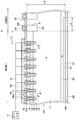
- the semiconductor device of the first embodiment will be described with reference to FIG.
- the semiconductor device according to the present embodiment includes a semiconductor substrate 10 having one surface 10a and another surface 10b opposite to the one surface 10a, and an element portion 1 on which an IGBT element is formed, and the element portion. 1 and the outer peripheral part 2 surrounding 1 are formed.
- a basic configuration of the element unit 1 will be described.
- the element section 1 has an N ⁇ type drift layer 11, and a P type base layer 12 is formed on the drift layer 11 (that is, on the one surface 10 a side of the semiconductor substrate 10).
- a plurality of trenches 13 that penetrate the base layer 12 and reach the drift layer 11 are formed, and the base layer 12 is divided by the plurality of trenches 13.
- the plurality of trenches 13 are formed at regular intervals in a stripe shape along one direction (that is, the depth direction in the drawing in FIG. 1) of the surface direction of the one surface 10a of the semiconductor substrate 10.
- the impurity concentration of the drift layer 11 is 1.0 ⁇ 10 14 cm ⁇ 3 .
- the plurality of trenches 13 are formed so that the distance between the side surfaces facing each other is constant. That is, the interval between adjacent trenches 13 is constant along the bottom side from the opening side of the trench 13.
- each gate electrode 15 is appropriately electrically connected to the gate pad 4 through the gate wiring 3 so that a predetermined gate voltage can be applied from an external gate circuit.
- N + -type emitter region 16 and a P + -type body region 17 are formed in the surface layer portion of the base layer 12.
- the emitter region 16 is configured to have a higher impurity concentration than the drift layer 11, is terminated in the base layer 12, and is in contact with the side surface of the trench 13.
- the body region 17 has a higher impurity concentration than the base layer 12 and is formed so as to terminate in the base layer 12, similarly to the emitter region 16.
- the emitter region 16 extends in a rod shape so as to be in contact with the side surface of the trench 13 along the longitudinal direction of the trench 13 in the region between the trenches 13 and terminates inside the tip of the trench 13.
- the body region 17 is sandwiched between the two emitter regions 16 and extends in a rod shape along the longitudinal direction of the trench 13 (that is, the emitter region 16). Note that the body region 17 of the present embodiment is formed deeper than the emitter region 16 with respect to the one surface 10 a of the semiconductor substrate 10.
- An interlayer insulating film 18 made of BPSG (abbreviation of Boro-phosphosilicate glass) or the like is formed on one surface 10 a of the semiconductor substrate 10.
- BPSG abbreviation of Boro-phosphosilicate glass
- An upper electrode 19 electrically connected to the emitter region 16 and the body region 17 is formed on the interlayer insulating film 18 through the first contact hole 18a.
- An N-type field stop layer (hereinafter simply referred to as an FS layer) 20 is formed on the side of the drift layer 11 opposite to the base layer 12 side (that is, the other surface 10b side of the semiconductor substrate 10).
- this FS layer 20 is not necessarily required, it is possible to improve the breakdown voltage and steady loss performance by preventing the depletion layer from spreading, and to increase the injection amount of holes injected from the other surface 10b side of the semiconductor substrate 10. Be prepared to control.
- a P-type collector layer 21 is formed on the opposite side of the drift layer 11 across the FS layer 20, and the collector layer 21 and the collector layer 21 are formed on the collector layer 21 (that is, on the other surface 10b of the semiconductor substrate 10).
- a lower electrode 22 to be electrically connected is formed.
- the outer peripheral part 2 has the same drift layer 11 as the element part 1.
- a P + -type deep layer 23 deeper than the base layer 12 is formed on the surface layer portion of the drift layer 11 so that electric field concentration of the element portion 1 is suppressed.
- the P + type deep layer 23 is formed so as to suppress the electric field concentration at the bottom of the trench 13.
- a plurality of deep layers 23 are formed, each having an annular structure surrounding the element portion 1. That is, the multiple deep layers 23 are formed so as to constitute a multiple ring structure.
- the deep layer 23 is formed so as to be deeper than the base layer 12. However, the deeper the deep layer 23, the thinner the drift layer 11 becomes and the lower the breakdown voltage. It is preferably formed so as to be deeper by about 3 ⁇ m. In the present embodiment, the deep layer 23 located closest to the element part 1 among the plurality of deep layers 23 is formed so as to be in contact with the base layer 12 formed in the element part 1. That is, it can be said that the deep layer 23 is formed continuously with the base layer 12.
- an interlayer insulating film 18 is formed on one surface 10 a of the semiconductor substrate 10, and a second contact hole 18 b that exposes the deep layer 23 is exposed in the interlayer insulating film 18. Is formed.
- An outer peripheral electrode 24 that is electrically connected to the deep layer 23 through the second contact hole 18b is formed on the interlayer insulating film 18.
- the FS layer 20 is formed on the other surface 10 b side of the semiconductor substrate 10 in the outer peripheral portion 2.
- the lower electrode 22 is formed on the FS layer 20 (that is, on the other surface 10 b of the semiconductor substrate 10).
- N + type and N ⁇ type correspond to the first conductivity type
- P type and P + type correspond to the second conductivity type
- the upper electrode 19 corresponds to the first electrode
- the lower electrode 22 corresponds to the second electrode.
- the semiconductor device when a predetermined gate voltage is applied to the gate electrode 15 from an external gate circuit while the upper electrode 19 is grounded and a positive voltage is applied to the lower electrode 22, An inversion layer (that is, a channel region) is formed at a portion in contact with the trench 13.
- An inversion layer that is, a channel region
- electrons are supplied from the emitter region 16 to the drift layer 11 through the inversion layer, and holes are supplied from the collector layer 21 to the drift layer 11.
- the resistance value of the drift layer 11 decreases due to conductivity modulation, and a current flows between the upper electrode 19 and the lower electrode 22.
- a positive voltage is applied to the upper electrode 19 and the lower electrode 22 is grounded.
- a voltage of 0 V is applied to the gate electrode 15, the upper electrode 19, the lower electrode 22,
- the current that was flowing during is interrupted.
- a state in which a current flows between the upper electrode 19 and the lower electrode 22 is that the semiconductor device is on, and a state in which the current is interrupted is that the semiconductor device is in an off state.
- electrons correspond to first carriers and holes correspond to second carriers.
- the positional relationship between the emitter region 16 and the collector layer 21 is adjusted so that the occurrence of breakdown is suppressed in the outer peripheral portion 2 when changing from the on state to the off state. That is, when the deep layer 23 deeper than the base layer 12 is formed in the outer peripheral portion 2 as described above, the substantial thickness of the drift layer 11 in the outer peripheral portion 2 is reduced, and the breakdown voltage of the outer peripheral portion 2 is likely to be reduced. For this reason, in the present embodiment, the positional relationship between the emitter region 16 and the collector layer 21 is adjusted so that breakdown does not easily occur in the outer peripheral portion 2 even if the withstand voltage decreases.
- the breakdown voltage of the outer peripheral portion 2 is reduced by forming the deep layer 23, the positional relationship between the emitter region 16 and the collector layer 21 so that the carrier density of the outer peripheral portion 2 is lowered based on the reduced breakdown voltage. Has been adjusted.
- the positional relationship between the emitter region 16 and the collector layer 21 will be specifically described.
- the position closest to the element part 1 in the deep layer 23 is defined as a boundary position K between the element part 1 and the outer peripheral part 2.
- the position on the outermost peripheral portion 2 side (hereinafter referred to as the outermost emitter position) and the boundary position A distance from K is a first distance L1.
- the distance between the position of the end portion of the collector layer 21 along the surface direction of the semiconductor substrate 10 and the boundary position K is defined as a second distance L2.
- the second distance L2 is a positive distance when the position of the end portion of the collector layer 21 along the surface direction of the semiconductor substrate 10 is located in the element portion 1, and the position of the end portion is at the outer peripheral portion 2. If it is located, the distance is negative. Further, the thickness of the semiconductor substrate 10 is set to the third distance L3. The distance between the narrowest portions of the intervals between adjacent trenches 13 is defined as a trench interval L4.
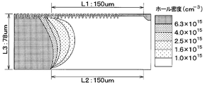
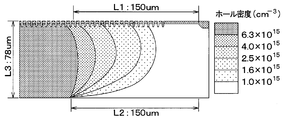
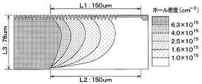
- the semiconductor device of this embodiment when a predetermined gate voltage is applied to the gate electrode 15, electrons are supplied from the emitter region 16 to the drift layer 11 and holes are generated from the collector layer 21. By being supplied to the drift layer 11, it is turned on. At this time, as shown in FIGS. 2A to 2C, it is confirmed that the hole density distribution varies depending on the trench interval d4. Then, it is confirmed that the narrower the trench interval d4, the larger the spread of the portion having a higher hole density. That is, in FIGS. 2A to 2C, the portion with the highest hole density in FIG. 2A to 2C show simulation results in which the first distance L1 is 150 ⁇ m, the second distance L2 is 150 ⁇ m, and the third distance L3 is 78 ⁇ m.
- the present inventors have examined the carrier spread on one side with respect to the plate thickness based on the trench interval L4, and obtained the results shown in FIG. That is, as shown in FIG. 3, the carrier spread A on one side with respect to the plate thickness (hereinafter simply referred to as carrier spread A) is represented by the following equation using the trench interval L4.
- Equation 1 ⁇ 0.30 ⁇ L4 + 1.53
- the carrier spread A in this embodiment is defined as follows. That is, the carrier spread A is based on the portion immediately below the outermost emitter position in the portion of the drift layer 11 closest to the one surface 10a of the semiconductor substrate 10, and the hole density is 10 times the impurity concentration of the drift layer 11 from the reference. Let us show how far the part is. In the present embodiment, since the impurity concentration of the drift layer 11 is set to 1.0 ⁇ 10 14 cm ⁇ 3 , it shows how far the portion that becomes 1.0 ⁇ 10 15 cm ⁇ 3 is separated.
- the hole density is 1.0 ⁇ 10 15 cm from the portion immediately below the outermost emitter position in the portion of the drift layer 11 closest to the one surface 10 a of the semiconductor substrate 10.
- a portion that is less than ⁇ 3 means a portion that is separated by 39 ⁇ m (that is, half the plate thickness) or more on the outer peripheral portion 2 side.
- the part where the hole density is 10 times the impurity concentration of the drift layer 11 is used as a boundary.
- the hole density exceeds 10 times the impurity concentration of the drift layer 11, the electric field strength is increased due to the positive charges of the holes. This is because the pressure drop is significantly reduced.
- the carrier spread A is a ratio to the plate thickness, the plate thickness ⁇ A is a position where the hole density is 1.0 ⁇ 10 15 cm ⁇ 3 from the reference.
- the portion of the drift layer 11 closest to the surface 10 a of the semiconductor substrate 10 is the boundary position with the base layer 12 in the case of the element portion 1. And if it is the outer peripheral part 2, it will be a boundary position with the deep layer 23. However, in the case of the outer peripheral portion 2, in the portion where the deep layer 23 is not formed, the position of the same depth as the boundary position of the portion where the deep layer 23 is formed is the most surface of the semiconductor substrate 10 in the drift layer 11. 10a side portion.
- the trench interval d4 is preferably formed at least about 100 nm apart so that the inversion layers formed along the adjacent trenches 13 are not connected to each other. Furthermore, if the trench interval d4 is too wide, the effect of accumulating holes in the drift layer 11 is remarkably reduced, so that it is preferably 8 ⁇ m or less.
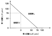
- FIG. 4 shows a simulation result when the trench interval L4 is 1.8 ⁇ m and the third distance L3 is 78 ⁇ m. That is, FIG. 4 shows a simulation result when the carrier spread A is 1. In other words, it is a simulation result when the length between the reference and the portion where the hole density is 1.0 ⁇ 10 15 cm ⁇ 3 is 78 ⁇ 1.
- Equation 2 L1 ⁇ 78 ⁇ 1-L2
- Equation 2 Equation 2
- Equation 3 L1 ⁇ L3 ⁇ A ⁇ L2
- L4 is set. For this reason, when changing from the on state to the off state, breakdown can be prevented from occurring in the outer peripheral portion 2, and the semiconductor device can be prevented from being destroyed.
- L1 L3 ⁇ ( ⁇ 0.30 ⁇ L4 + 1.53) ⁇ L2
- L1 L3 ⁇ ( ⁇ 0.30 ⁇ L4 + 1.53) ⁇ L2
- L1 L3 ⁇ ( ⁇ 0.30 ⁇ L4 + 1.53) ⁇ L2
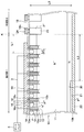
- FIG. 1 shows that the position of the end portion along the surface direction of the semiconductor substrate 10 in the collector layer 21 is located in the element portion 1.
- the position of the end portion along the surface direction of the semiconductor substrate 10 in the collector layer 21 may be located in the outer peripheral portion 2 as shown in FIG.
- the second distance L2 is a negative value.
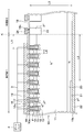
- a part of the gate electrodes 15 a among the plurality of gate electrodes 15 is connected to the gate pad 4.
- the remaining gate electrode 15 b of the plurality of gate electrodes 15 is not connected to the gate pad 4 but connected to the upper electrode 19 through the third contact hole 18 c formed in the interlayer insulating film 18. Yes. That is, the gate electrode 15b connected to the upper electrode 19 is a so-called dummy gate electrode that does not exhibit a function of forming an inversion layer in the base layer 12 when the semiconductor device is in an on state.
- the first gate electrode 15a and the second gate electrode 15b are formed on the surface of the semiconductor substrate 10. Alternatingly arranged along the direction.
- the first gate electrode 15a and the second gate electrode 15b are arranged such that the second gate electrode 15b is located on the outermost peripheral part 2 side in the arrangement direction of the first gate electrode 15a and the second gate electrode 15b. Yes.
- the emitter region 16 is formed along each trench 13 as in the first embodiment. That is, in this embodiment, the emitter region 16 is also formed on the side surface of the trench 13 in which the second gate electrode 15b is disposed.
- the first distance L1 is a distance between the outermost emitter position and the boundary position K as described above. For this reason, in the semiconductor device of this embodiment, the emitter region 16 in contact with the trench 13 in which the first gate electrode 15a is disposed, and the distance between the position on the outermost peripheral portion 2 side and the boundary position K is the first. One distance L1.
- each trench 13 has a width on the bottom side longer than a width on the opening side in the interval between the opposing side surfaces.
- the interval between the adjacent trenches 13 is such that the interval on the bottom side is shorter than the interval on the opening side. That is, in the present embodiment, the trench 13 has a so-called bowl shape.
- the trench interval L4 is the narrowest portion of the intervals between adjacent trenches 13 as described above. For this reason, in this embodiment, the trench interval L4 is a portion on the bottom side of the portion between the adjacent trenches 13.
- the manufacturing process of the emitter region 16 and the body region 17 can be simplified, and the first The same effect as that of the first embodiment can be obtained.
- the first conductivity type is N type and the second conductivity type is P type.
- the first conductivity type is P type
- the second conductivity type is N type. You can also.
- the emitter region 16 may not be formed so as to be in contact with the side surface of the trench 13 in which the second gate electrode 15b is disposed. That is, the emitter region 16 may be formed only on the side surface of the trench 13 in which the first gate electrode 15a is disposed.
- the second gate electrode 15b may not be connected to the upper electrode 19 but may be connected to a gate pad different from the gate pad 4 and maintained at a predetermined potential (for example, ground potential). It may be in a floating state without being connected to.
- the first gate electrode 15a may be located on the outermost peripheral portion 2 side in the arrangement direction of the first gate electrode 15a and the second gate electrode 15b.
- the second embodiment may be combined with the third embodiment, and the semiconductor device of the third embodiment may be configured to have the first gate electrode 15a and the second gate electrode 15b.
Abstract
This semiconductor device has an element part (1) and an outer peripheral part (2) surrounding the element part (1), wherein a deep layer (23) is formed more deeply in the outer peripheral part (2) than in a base layer (12). When the position which, in the deep layers (23), is closest to the element part (1) is a boundary position (K), the distance between the boundary position (K) and the position which is closest to the outer peripheral part (2) in an emitter region (16) into which first carriers can be injected is a first distance (L1), and the distance between the boundary position (K) and the position of a stepped part in a surface direction of a semiconductor substrate (10) in a collector layer (21) is a second distance (L2), the first distance (L1) and the second distance (L2) are adjusted so that a carrier density at the outer peripheral part (2) is decreased on the basis of the withstand voltage of the outer peripheral part (2), the withstand voltage having been decreased by the deep layer (23).
Description
本出願は、2017年2月3日に出願された日本特許出願番号2017-18672号に基づくもので、ここにその記載内容が参照により組み入れられる。
This application is based on Japanese Patent Application No. 2017-18672 filed on Feb. 3, 2017, the contents of which are incorporated herein by reference.
本発明は、絶縁ゲートバイポーラトランジスタ(以下では、単にIGBTという)素子が形成された素子部と、素子部を取り囲む外周部とを有する半導体装置に関する。
The present invention relates to a semiconductor device having an element part in which an insulated gate bipolar transistor (hereinafter simply referred to as IGBT) element is formed and an outer peripheral part surrounding the element part.
従来より、IGBT素子が形成された素子部と、この素子部を取り囲む外周部とを有する半導体装置が提案されている(例えば、特許文献1参照)。具体的には、この半導体装置は、一面および一面と反対側の他面を有し、ドリフト層を構成する半導体基板を備えている。そして、素子部では、ドリフト層上にP型のベース層が形成され、ベース層の表層部にN+型のエミッタ領域が形成されている。また、ゲート絶縁膜を介してベース層と接するように、ゲート電極が形成されている。そして、ドリフト層のうちのベース層と反対側には、コレクタ層が形成されている。なお、このコレクタ層は、素子部から外周部に渡って形成されている。また、半導体基板の一面側には、ベース層およびエミッタ領域と電気的に接続されるように上部電極が形成され、半導体基板の他面側には、コレクタ層と電気的に接続されるように下部電極が形成されている。
Conventionally, a semiconductor device having an element part in which an IGBT element is formed and an outer peripheral part surrounding the element part has been proposed (see, for example, Patent Document 1). Specifically, this semiconductor device includes a semiconductor substrate that has one surface and another surface opposite to the one surface and forms a drift layer. In the element portion, a P-type base layer is formed on the drift layer, and an N + -type emitter region is formed on the surface layer portion of the base layer. A gate electrode is formed so as to be in contact with the base layer through the gate insulating film. A collector layer is formed on the side of the drift layer opposite to the base layer. The collector layer is formed from the element portion to the outer peripheral portion. An upper electrode is formed on one side of the semiconductor substrate so as to be electrically connected to the base layer and the emitter region, and is connected to a collector layer on the other side of the semiconductor substrate. A lower electrode is formed.
外周部では、半導体基板の一面側に複数のP+型のディープ層が多重リング構造を構成するように形成されている。なお、複数のディープ層は、素子部の電界集中が抑制されるように、ベース層よりも深くまで形成されている。
In the outer peripheral portion, a plurality of P + type deep layers are formed on one surface side of the semiconductor substrate so as to form a multiple ring structure. The plurality of deep layers are formed deeper than the base layer so that the electric field concentration in the element portion is suppressed.
このような半導体装置では、ゲート電極に所定のゲート電圧が印加されると、ベース層のうちのゲート電極と隣接する部分に反転層(すなわち、チャネル領域)が形成される。これにより、エミッタ領域から反転層を介して電子がドリフト層に供給されると共に、コレクタ層からホールがドリフト層に供給され、伝導度変調によってドリフト層の抵抗値が低下して電流が流れる。
In such a semiconductor device, when a predetermined gate voltage is applied to the gate electrode, an inversion layer (that is, a channel region) is formed in a portion of the base layer adjacent to the gate electrode. As a result, electrons are supplied from the emitter region to the drift layer via the inversion layer, and holes are supplied from the collector layer to the drift layer, and the resistance value of the drift layer is lowered by conductivity modulation, and current flows.
しかしながら、上記半導体装置では、外周部にベース層よりも深いディープ層が形成されているため、外周部では、ドリフト層の実質的な厚さが素子部よりも薄くなって耐圧が低下してしまう。また、上記半導体装置では、コレクタ層が外周部にも形成されており、外周部に形成されたコレクタ層からもホールがドリフト層に供給される。このため、上記半導体装置では、電流が流れている状態から当該電流を遮断する際、外周部でブレークダウンが発生し易くなる。そして、上記半導体装置は、外周部では素子部よりも電流を掃き出し難いため、外周部でブレークダウンが発生すると破壊されてしまう可能性が高くなる。
However, in the semiconductor device, since the deep layer deeper than the base layer is formed at the outer peripheral portion, the substantial thickness of the drift layer is thinner than the element portion at the outer peripheral portion, and the breakdown voltage decreases. . In the semiconductor device, the collector layer is also formed on the outer peripheral portion, and holes are also supplied to the drift layer from the collector layer formed on the outer peripheral portion. For this reason, in the semiconductor device, when the current is interrupted from the state where the current flows, breakdown is likely to occur at the outer peripheral portion. Since the semiconductor device is less likely to sweep out current at the outer peripheral portion than at the element portion, there is a high possibility that the semiconductor device will be destroyed if breakdown occurs at the outer peripheral portion.
本開示は、外周部にベース層よりも深くまで形成されたディープ層を有する半導体装置において、外周部でブレークダウンが発生することを抑制できる半導体装置を提供することを目的とする。
An object of the present disclosure is to provide a semiconductor device having a deep layer formed deeper than the base layer in the outer peripheral portion and capable of suppressing the occurrence of breakdown in the outer peripheral portion.
本開示の1つの観点によれば、素子部と、素子部を取り囲む外周部とを有する半導体装置は、一面および一面と反対側の他面を有し、第1導電型のドリフト層を構成する半導体基板と、素子部におけるドリフト層上であって、半導体基板の一面側に形成された第2導電型のベース層と、ベース層を貫通してドリフト層に達し、半導体基板の面方向に沿って延設された複数のトレンチの壁面にそれぞれ形成されたゲート絶縁膜と、ゲート絶縁膜上にそれぞれ形成されたゲート電極と、ベース層の表層部に形成され、トレンチと接する第1導電型のエミッタ領域と、外周部におけるドリフト層の表層部であって、半導体基板の一面側に形成され、ベース層よりも深さが深くされた第2導電型のディープ層と、少なくとも素子部における半導体基板の他面側に形成された第2導電型のコレクタ層と、エミッタ領域およびベース層と電気的に接続される第1電極と、コレクタ層と電気的に接続される第2電極と、を備えている。そして、半導体装置は、ゲート電極に所定のゲート電圧が印加されることにより、第1電極からエミッタ領域を介してドリフト層に第1キャリアが注入されると共に第2電極からコレクタ層を介してドリフト層に第2キャリアが注入されることで第1電極と第2電極との間に電流を流し、半導体基板の一面において、ディープ層における最も素子部側の位置を境界位置とし、境界位置と、第1電極から第1キャリアが注入され得るエミッタ領域のうちの最も外周部側の位置との間の距離を第1距離とし、境界位置と、コレクタ層のうちの半導体基板の面方向における端部の位置との間の距離を第2距離とすると、第1距離および第2距離は、ディープ層によって低下した外周部の耐圧に基づいて当該外周部におけるキャリア密度が低下するように調整されている。
According to one aspect of the present disclosure, a semiconductor device having an element portion and an outer peripheral portion surrounding the element portion has one surface and another surface opposite to the one surface, and constitutes a first conductivity type drift layer. A semiconductor substrate, a second conductivity type base layer formed on one surface side of the semiconductor substrate on the drift layer in the element portion, and reaches the drift layer through the base layer, along the surface direction of the semiconductor substrate A gate insulating film formed on each of the wall surfaces of the plurality of trenches extended, a gate electrode formed on the gate insulating film, and a first conductivity type formed on a surface layer portion of the base layer and in contact with the trench An emitter region, a surface layer portion of the drift layer in the outer peripheral portion, formed on one surface side of the semiconductor substrate and deeper than the base layer, and a semiconductor substrate at least in the element portion A collector layer of a second conductivity type formed on the other surface side, a first electrode electrically connected to the emitter region and the base layer, and a second electrode electrically connected to the collector layer. ing. In the semiconductor device, when a predetermined gate voltage is applied to the gate electrode, first carriers are injected from the first electrode into the drift layer through the emitter region, and drift from the second electrode through the collector layer. A current flows between the first electrode and the second electrode by injecting the second carrier into the layer, and on one surface of the semiconductor substrate, the position closest to the element portion in the deep layer is defined as a boundary position, The distance between the first electrode and the position on the outermost peripheral side of the emitter region where the first carriers can be injected is defined as the first distance, and the boundary position and the end of the collector layer in the plane direction of the semiconductor substrate If the distance between the first and second positions is the second distance, the carrier density in the outer peripheral portion of the first distance and the second distance is reduced based on the breakdown voltage of the outer peripheral portion reduced by the deep layer. It has been adjusted to.
これによれば、電流が流れている状態から当該電流を遮断する際、外周部でブレークダウンが発生することを抑制でき、半導体装置が破壊されることを抑制できる。
According to this, when the current is interrupted from the state where the current is flowing, it is possible to suppress the breakdown from occurring in the outer peripheral portion, and it is possible to suppress the destruction of the semiconductor device.
以下、本開示の実施形態について図に基づいて説明する。なお、以下の各実施形態相互において、互いに同一もしくは均等である部分には、同一符号を付して説明を行う。
Hereinafter, embodiments of the present disclosure will be described with reference to the drawings. In the following embodiments, parts that are the same or equivalent to each other will be described with the same reference numerals.
(第1実施形態)
第1実施形態の半導体装置について図1を参照しつつ説明する。図1に示されるように、本実施形態の半導体装置は、一面10aおよび一面10aと反対側の他面10bを有する半導体基板10を備え、IGBT素子が形成された素子部1と、この素子部1を取り囲む外周部2とが形成されている。まず、素子部1の基本的な構成について説明する。 (First embodiment)
The semiconductor device of the first embodiment will be described with reference to FIG. As shown in FIG. 1, the semiconductor device according to the present embodiment includes asemiconductor substrate 10 having one surface 10a and another surface 10b opposite to the one surface 10a, and an element portion 1 on which an IGBT element is formed, and the element portion. 1 and the outer peripheral part 2 surrounding 1 are formed. First, a basic configuration of the element unit 1 will be described.
第1実施形態の半導体装置について図1を参照しつつ説明する。図1に示されるように、本実施形態の半導体装置は、一面10aおよび一面10aと反対側の他面10bを有する半導体基板10を備え、IGBT素子が形成された素子部1と、この素子部1を取り囲む外周部2とが形成されている。まず、素子部1の基本的な構成について説明する。 (First embodiment)
The semiconductor device of the first embodiment will be described with reference to FIG. As shown in FIG. 1, the semiconductor device according to the present embodiment includes a
素子部1は、N-型のドリフト層11を有し、ドリフト層11上(すなわち、半導体基板10の一面10a側)にP型のベース層12が形成されている。また、ベース層12を貫通してドリフト層11に達する複数のトレンチ13が形成されており、ベース層12は複数のトレンチ13によって分断されている。本実施形態では、複数のトレンチ13は、半導体基板10の一面10aの面方向のうちの一方向(すなわち、図1中紙面奥行き方向)に沿ってストライプ状に等間隔に形成されている。
The element section 1 has an N − type drift layer 11, and a P type base layer 12 is formed on the drift layer 11 (that is, on the one surface 10 a side of the semiconductor substrate 10). A plurality of trenches 13 that penetrate the base layer 12 and reach the drift layer 11 are formed, and the base layer 12 is divided by the plurality of trenches 13. In the present embodiment, the plurality of trenches 13 are formed at regular intervals in a stripe shape along one direction (that is, the depth direction in the drawing in FIG. 1) of the surface direction of the one surface 10a of the semiconductor substrate 10.
なお、本実施形態では、ドリフト層11の不純物濃度が1.0×1014cm-3とされている。また、複数のトレンチ13は、それぞれ対向する側面の間隔が一定となるように形成されている。つまり、隣接するトレンチ13の間隔は、トレンチ13の開口部側から底部側に沿って一定とされている。
In the present embodiment, the impurity concentration of the drift layer 11 is 1.0 × 10 14 cm −3 . Further, the plurality of trenches 13 are formed so that the distance between the side surfaces facing each other is constant. That is, the interval between adjacent trenches 13 is constant along the bottom side from the opening side of the trench 13.
複数のトレンチ13は、それぞれトレンチ13の壁面を覆うように形成されたゲート絶縁膜14と、当該ゲート絶縁膜14の上に形成されたゲート電極15とにより埋め込まれている。これにより、トレンチゲート構造が構成されている。なお、本実施形態では、各ゲート電極15は、適宜ゲート配線3を介してゲートパッド4と電気的に接続され、外部のゲート回路から所定のゲート電圧が印加され得るようになっている。
The plurality of trenches 13 are embedded with a gate insulating film 14 formed so as to cover the wall surface of the trench 13 and a gate electrode 15 formed on the gate insulating film 14. Thereby, a trench gate structure is configured. In the present embodiment, each gate electrode 15 is appropriately electrically connected to the gate pad 4 through the gate wiring 3 so that a predetermined gate voltage can be applied from an external gate circuit.
ベース層12の表層部には、N+型のエミッタ領域16およびP+型のボディ領域17が形成されている。具体的には、エミッタ領域16は、ドリフト層11よりも高不純物濃度で構成され、ベース層12内において終端し、かつ、トレンチ13の側面に接するように形成されている。一方、ボディ領域17は、ベース層12よりも高不純物濃度で構成され、エミッタ領域16と同様に、ベース層12内において終端するように形成されている。
An N + -type emitter region 16 and a P + -type body region 17 are formed in the surface layer portion of the base layer 12. Specifically, the emitter region 16 is configured to have a higher impurity concentration than the drift layer 11, is terminated in the base layer 12, and is in contact with the side surface of the trench 13. On the other hand, the body region 17 has a higher impurity concentration than the base layer 12 and is formed so as to terminate in the base layer 12, similarly to the emitter region 16.
より詳しくは、エミッタ領域16は、トレンチ13間の領域において、トレンチ13の長手方向に沿ってトレンチ13の側面に接するように棒状に延設され、トレンチ13の先端よりも内側で終端する構造とされている。また、ボディ領域17は、2つのエミッタ領域16に挟まれてトレンチ13の長手方向(すなわち、エミッタ領域16)に沿って棒状に延設されている。なお、本実施形態のボディ領域17は、半導体基板10の一面10aを基準としてエミッタ領域16よりも深く形成されている。
More specifically, the emitter region 16 extends in a rod shape so as to be in contact with the side surface of the trench 13 along the longitudinal direction of the trench 13 in the region between the trenches 13 and terminates inside the tip of the trench 13. Has been. The body region 17 is sandwiched between the two emitter regions 16 and extends in a rod shape along the longitudinal direction of the trench 13 (that is, the emitter region 16). Note that the body region 17 of the present embodiment is formed deeper than the emitter region 16 with respect to the one surface 10 a of the semiconductor substrate 10.
半導体基板10の一面10a上には、BPSG(Boro-phospho silicate glassの略)等で構成される層間絶縁膜18が形成されている。層間絶縁膜18には、エミッタ領域16の一部およびボディ領域17を露出させる第1コンタクトホール18aが形成されている。そして、層間絶縁膜18上には、第1コンタクトホール18aを介してエミッタ領域16およびボディ領域17と電気的に接続される上部電極19が形成されている。
An interlayer insulating film 18 made of BPSG (abbreviation of Boro-phosphosilicate glass) or the like is formed on one surface 10 a of the semiconductor substrate 10. In the interlayer insulating film 18, a first contact hole 18a exposing a part of the emitter region 16 and the body region 17 is formed. An upper electrode 19 electrically connected to the emitter region 16 and the body region 17 is formed on the interlayer insulating film 18 through the first contact hole 18a.
ドリフト層11のうちのベース層12側と反対側(すなわち、半導体基板10の他面10b側)には、N型のフィールドストップ層(以下では、単にFS層という)20が形成されている。このFS層20は、必ずしも必要なものではないが、空乏層の広がりを防ぐことで耐圧と定常損失の性能向上を図ると共に、半導体基板10の他面10b側から注入されるホールの注入量を制御するために備えてある。
An N-type field stop layer (hereinafter simply referred to as an FS layer) 20 is formed on the side of the drift layer 11 opposite to the base layer 12 side (that is, the other surface 10b side of the semiconductor substrate 10). Although this FS layer 20 is not necessarily required, it is possible to improve the breakdown voltage and steady loss performance by preventing the depletion layer from spreading, and to increase the injection amount of holes injected from the other surface 10b side of the semiconductor substrate 10. Be prepared to control.
そして、FS層20を挟んでドリフト層11と反対側には、P型のコレクタ層21が形成され、コレクタ層21上(すなわち、半導体基板10の他面10b上)には、コレクタ層21と電気的に接続される下部電極22が形成されている。
A P-type collector layer 21 is formed on the opposite side of the drift layer 11 across the FS layer 20, and the collector layer 21 and the collector layer 21 are formed on the collector layer 21 (that is, on the other surface 10b of the semiconductor substrate 10). A lower electrode 22 to be electrically connected is formed.
以上が本実施形態における素子部1の基本的な構成である。続いて、外周部2の基本的な構成について説明する。
The above is the basic configuration of the element unit 1 in the present embodiment. Subsequently, a basic configuration of the outer peripheral portion 2 will be described.
外周部2は、素子部1と同様のドリフト層11を有している。そして、ドリフト層11の表層部には、素子部1の電界集中が抑制されるように、ベース層12よりも深くされたP+型のディープ層23が形成されている。具体的には、外周部2には、素子部1ではトレンチ13の底部に電界集中が発生し易いため、トレンチ13の底部の電界集中が抑制されるようにP+型のディープ層23が形成されている。本実施形態では、ディープ層23は、複数形成されており、それぞれ素子部1を囲む環状構造とされている。つまり、複数のディープ層23は、多重リング構造を構成するように形成されている。
The outer peripheral part 2 has the same drift layer 11 as the element part 1. A P + -type deep layer 23 deeper than the base layer 12 is formed on the surface layer portion of the drift layer 11 so that electric field concentration of the element portion 1 is suppressed. Specifically, since the electric field concentration is likely to occur at the bottom of the trench 13 in the element portion 1 at the outer peripheral portion 2, the P + type deep layer 23 is formed so as to suppress the electric field concentration at the bottom of the trench 13. Has been. In the present embodiment, a plurality of deep layers 23 are formed, each having an annular structure surrounding the element portion 1. That is, the multiple deep layers 23 are formed so as to constitute a multiple ring structure.
なお、ディープ層23は、ベース層12より深くなるように形成されているが、深くするほどドリフト層11の実質的な厚さが薄くなって耐圧が低下するため、ベース層12よりも1~3μm程度深くなるように形成することが好ましい。また、本実施形態では、複数のディープ層23のうちの最も素子部1側に位置するディープ層23は、素子部1に形成されたベース層12と接触するように形成されている。つまり、このディープ層23は、ベース層12と連なって形成されているともいえる。
The deep layer 23 is formed so as to be deeper than the base layer 12. However, the deeper the deep layer 23, the thinner the drift layer 11 becomes and the lower the breakdown voltage. It is preferably formed so as to be deeper by about 3 μm. In the present embodiment, the deep layer 23 located closest to the element part 1 among the plurality of deep layers 23 is formed so as to be in contact with the base layer 12 formed in the element part 1. That is, it can be said that the deep layer 23 is formed continuously with the base layer 12.
また、外周部2では、素子部1と同様に、半導体基板10の一面10a上に層間絶縁膜18が形成されており、層間絶縁膜18には、ディープ層23を露出させる第2コンタクトホール18bが形成されている。そして、層間絶縁膜18上には、第2コンタクトホール18bを介してディープ層23と電気的に接続される外周電極24が形成されている。
In the outer peripheral portion 2, similarly to the element portion 1, an interlayer insulating film 18 is formed on one surface 10 a of the semiconductor substrate 10, and a second contact hole 18 b that exposes the deep layer 23 is exposed in the interlayer insulating film 18. Is formed. An outer peripheral electrode 24 that is electrically connected to the deep layer 23 through the second contact hole 18b is formed on the interlayer insulating film 18.
外周部2における半導体基板10の他面10b側は、FS層20が形成されている。そして、外周部2では、FS層20上(すなわち、半導体基板10の他面10b上)に下部電極22が形成されている。
The FS layer 20 is formed on the other surface 10 b side of the semiconductor substrate 10 in the outer peripheral portion 2. In the outer peripheral portion 2, the lower electrode 22 is formed on the FS layer 20 (that is, on the other surface 10 b of the semiconductor substrate 10).
以上が本実施形態における半導体装置の基本的な構成である。なお、本実施形態では、N+型、N-型が第1導電型に相当しており、P型、P+型が第2導電型に相当している。また、上部電極19が第1電極に相当し、下部電極22が第2電極に相当している。
The above is the basic configuration of the semiconductor device according to the present embodiment. In the present embodiment, N + type and N − type correspond to the first conductivity type, and P type and P + type correspond to the second conductivity type. The upper electrode 19 corresponds to the first electrode, and the lower electrode 22 corresponds to the second electrode.
次に、上記半導体装置の基本的な作動について説明する。上記半導体装置は、上部電極19が接地されると共に下部電極22に正の電圧が印加された状態でゲート電極15に外部のゲート回路から所定のゲート電圧が印加されると、ベース層12のうちのトレンチ13と接する部分に反転層(すなわち、チャネル領域)が形成される。そして、半導体装置は、エミッタ領域16から反転層を介して電子がドリフト層11に供給されると共に、コレクタ層21からホールがドリフト層11に供給される。これにより、半導体装置は、伝導度変調によってドリフト層11の抵抗値が低下し、上部電極19と下部電極22との間に電流が流れる。
Next, the basic operation of the semiconductor device will be described. In the semiconductor device, when a predetermined gate voltage is applied to the gate electrode 15 from an external gate circuit while the upper electrode 19 is grounded and a positive voltage is applied to the lower electrode 22, An inversion layer (that is, a channel region) is formed at a portion in contact with the trench 13. In the semiconductor device, electrons are supplied from the emitter region 16 to the drift layer 11 through the inversion layer, and holes are supplied from the collector layer 21 to the drift layer 11. Thereby, in the semiconductor device, the resistance value of the drift layer 11 decreases due to conductivity modulation, and a current flows between the upper electrode 19 and the lower electrode 22.
そして、上記半導体装置は、上部電極19に正の電圧が印加されると共に下部電極22が接地され、例えば、ゲート電極15に0Vの電圧が印加されることにより、上部電極19と下部電極22との間に流れていた電流が遮断される。なお、以下では、上部電極19と下部電極22との間に電流が流れている状態を半導体装置がオン状態であるとし、当該電流が遮断された状態を半導体装置がオフ状態であるとして説明する。また、本実施形態では、電子が第1キャリアに相当し、ホールが第2キャリアに相当している。
In the semiconductor device, a positive voltage is applied to the upper electrode 19 and the lower electrode 22 is grounded. For example, when a voltage of 0 V is applied to the gate electrode 15, the upper electrode 19, the lower electrode 22, The current that was flowing during is interrupted. In the following description, it is assumed that a state in which a current flows between the upper electrode 19 and the lower electrode 22 is that the semiconductor device is on, and a state in which the current is interrupted is that the semiconductor device is in an off state. . In the present embodiment, electrons correspond to first carriers and holes correspond to second carriers.
ここで、本実施形態では、オン状態からオフ状態にする際、外周部2にてブレークダウンの発生が抑制されるように、エミッタ領域16およびコレクタ層21の位置関係が調整されている。すなわち、上記のように、外周部2にベース層12より深いディープ層23を形成すると、外周部2におけるドリフト層11の実質的な厚さが薄くなり、外周部2の耐圧が低くなり易い。このため、本実施形態では、耐圧が低下したとしても外周部2にてブレークダウンが発生し難いように、エミッタ領域16とコレクタ層21の位置関係が調整されている。言い換えると、ディープ層23を形成することによって外周部2の耐圧が低下するため、低下した耐圧に基づいて外周部2のキャリア密度が低くなるように、エミッタ領域16とコレクタ層21との位置関係が調整されている。
Here, in this embodiment, the positional relationship between the emitter region 16 and the collector layer 21 is adjusted so that the occurrence of breakdown is suppressed in the outer peripheral portion 2 when changing from the on state to the off state. That is, when the deep layer 23 deeper than the base layer 12 is formed in the outer peripheral portion 2 as described above, the substantial thickness of the drift layer 11 in the outer peripheral portion 2 is reduced, and the breakdown voltage of the outer peripheral portion 2 is likely to be reduced. For this reason, in the present embodiment, the positional relationship between the emitter region 16 and the collector layer 21 is adjusted so that breakdown does not easily occur in the outer peripheral portion 2 even if the withstand voltage decreases. In other words, since the breakdown voltage of the outer peripheral portion 2 is reduced by forming the deep layer 23, the positional relationship between the emitter region 16 and the collector layer 21 so that the carrier density of the outer peripheral portion 2 is lowered based on the reduced breakdown voltage. Has been adjusted.
以下に、エミッタ領域16およびコレクタ層21の位置関係について、具体的に説明する。なお、以下では、図1に示されるように、ディープ層23のうちの最も素子部1側の位置を素子部1と外周部2との境界位置Kとする。また、複数のエミッタ領域16のうちの上部電極19から電子(すなわち、キャリア)が注入され得るエミッタ領域16において、最も外周部2側の位置(以下では、最外エミッタ位置という)と、境界位置Kとの間の距離を第1距離L1とする。そして、コレクタ層21における半導体基板10の面方向に沿った端部の位置と、境界位置Kとの間の距離を第2距離L2とする。なお、第2距離L2は、コレクタ層21における半導体基板10の面方向に沿った端部の位置が素子部1内に位置する場合を正の距離とし、当該端部の位置が外周部2に位置する場合を負の距離とする。さらに、半導体基板10の板厚を第3距離L3とする。そして、隣接するトレンチ13の間隔のうちの最も狭い部分の距離をトレンチ間隔L4とする。
Hereinafter, the positional relationship between the emitter region 16 and the collector layer 21 will be specifically described. In the following, as shown in FIG. 1, the position closest to the element part 1 in the deep layer 23 is defined as a boundary position K between the element part 1 and the outer peripheral part 2. Further, in the emitter region 16 in which electrons (that is, carriers) can be injected from the upper electrode 19 among the plurality of emitter regions 16, the position on the outermost peripheral portion 2 side (hereinafter referred to as the outermost emitter position) and the boundary position A distance from K is a first distance L1. The distance between the position of the end portion of the collector layer 21 along the surface direction of the semiconductor substrate 10 and the boundary position K is defined as a second distance L2. The second distance L2 is a positive distance when the position of the end portion of the collector layer 21 along the surface direction of the semiconductor substrate 10 is located in the element portion 1, and the position of the end portion is at the outer peripheral portion 2. If it is located, the distance is negative. Further, the thickness of the semiconductor substrate 10 is set to the third distance L3. The distance between the narrowest portions of the intervals between adjacent trenches 13 is defined as a trench interval L4.
まず、上記のように、本実施形態の半導体装置は、ゲート電極15に所定のゲート電圧が印加されると、エミッタ領域16から電子がドリフト層11に供給されると共に、コレクタ層21からホールがドリフト層11に供給されることでオン状態となる。この際、図2A~図2Cに示されるように、トレンチ間隔d4によってホール密度の分布が異なることが確認される。そして、トレンチ間隔d4が狭いほど、ホール密度が高い部分の広がりが大きくなることが確認される。すなわち、図2A~図2Cでは、図2Cがホール密度の高い部分が最も広がっている。なお、図2A~図2Cは、第1距離L1を150μmとし、第2距離L2を150μmとし、第3距離L3を78μmとしたシミュレーション結果である。
First, as described above, in the semiconductor device of this embodiment, when a predetermined gate voltage is applied to the gate electrode 15, electrons are supplied from the emitter region 16 to the drift layer 11 and holes are generated from the collector layer 21. By being supplied to the drift layer 11, it is turned on. At this time, as shown in FIGS. 2A to 2C, it is confirmed that the hole density distribution varies depending on the trench interval d4. Then, it is confirmed that the narrower the trench interval d4, the larger the spread of the portion having a higher hole density. That is, in FIGS. 2A to 2C, the portion with the highest hole density in FIG. 2A to 2C show simulation results in which the first distance L1 is 150 μm, the second distance L2 is 150 μm, and the third distance L3 is 78 μm.
このため、本発明者らは、板厚に対する一面側のキャリア広がりについて、トレンチ間隔L4に基づいた検討を行い、図3に示す結果を得た。すなわち、図3に示されるように、板厚に対する一面側のキャリア広がりA(以下では、単にキャリア広がりAという)は、トレンチ間隔L4を用いた次式で示される。
For this reason, the present inventors have examined the carrier spread on one side with respect to the plate thickness based on the trench interval L4, and obtained the results shown in FIG. That is, as shown in FIG. 3, the carrier spread A on one side with respect to the plate thickness (hereinafter simply referred to as carrier spread A) is represented by the following equation using the trench interval L4.
(数1)A=-0.30×L4+1.53
なお、本実施形態におけるキャリア広がりAは、次のように定義される。すなわち、キャリア広がりAは、ドリフト層11における最も半導体基板10の一面10a側の部分において、最外エミッタ位置の直下の部分を基準とし、当該基準からホール密度がドリフト層11の不純物濃度の10倍となる部分がどれだけ離れているかを示すものとする。本実施形態では、ドリフト層11の不純物濃度が1.0×1014cm-3とされているため、1.0×1015cm-3となる部分がどれだけ離れているかを示している。言い換えると、基準から、ホール密度が1.0×1015cm-3以上となる部分と、ホール密度が1.0×1015cm-3未満となる部分との境界がどれだけ離れているかを示している。例えば、キャリア広がりAが1であれば、ドリフト層11における最も半導体基板10の一面10a側の部分において、最外エミッタ位置の直下の部分からホール密度が1.0×1015cm-3未満となる部分は、外周部2側に78μm(すなわち、板厚分)以上離れた部分であることを意味している。また、例えば、キャリア広がりAが0.5であれば、ドリフト層11における最も半導体基板10の一面10a側の部分において、最外エミッタ位置の直下の部分からホール密度が1.0×1015cm-3未満となる部分は、外周部2側に39μm(すなわち、板厚の半分)以上離れた部分であることを意味している。 (Equation 1) A = −0.30 × L4 + 1.53
Note that the carrier spread A in this embodiment is defined as follows. That is, the carrier spread A is based on the portion immediately below the outermost emitter position in the portion of thedrift layer 11 closest to the one surface 10a of the semiconductor substrate 10, and the hole density is 10 times the impurity concentration of the drift layer 11 from the reference. Let us show how far the part is. In the present embodiment, since the impurity concentration of the drift layer 11 is set to 1.0 × 10 14 cm −3 , it shows how far the portion that becomes 1.0 × 10 15 cm −3 is separated. In other words, how far is the boundary between the portion where the hole density is 1.0 × 10 15 cm −3 or more and the portion where the hole density is less than 1.0 × 10 15 cm −3 from the reference. Show. For example, if the carrier spread A is 1, the hole density is less than 1.0 × 10 15 cm −3 from the portion immediately below the outermost emitter position in the portion of the drift layer 11 closest to the one surface 10 a of the semiconductor substrate 10. This means that it is a part separated by 78 μm (that is, the thickness of the plate) or more on the outer peripheral part 2 side. For example, if the carrier spread A is 0.5, the hole density is 1.0 × 10 15 cm from the portion immediately below the outermost emitter position in the portion of the drift layer 11 closest to the one surface 10 a of the semiconductor substrate 10. A portion that is less than −3 means a portion that is separated by 39 μm (that is, half the plate thickness) or more on the outer peripheral portion 2 side.
なお、本実施形態におけるキャリア広がりAは、次のように定義される。すなわち、キャリア広がりAは、ドリフト層11における最も半導体基板10の一面10a側の部分において、最外エミッタ位置の直下の部分を基準とし、当該基準からホール密度がドリフト層11の不純物濃度の10倍となる部分がどれだけ離れているかを示すものとする。本実施形態では、ドリフト層11の不純物濃度が1.0×1014cm-3とされているため、1.0×1015cm-3となる部分がどれだけ離れているかを示している。言い換えると、基準から、ホール密度が1.0×1015cm-3以上となる部分と、ホール密度が1.0×1015cm-3未満となる部分との境界がどれだけ離れているかを示している。例えば、キャリア広がりAが1であれば、ドリフト層11における最も半導体基板10の一面10a側の部分において、最外エミッタ位置の直下の部分からホール密度が1.0×1015cm-3未満となる部分は、外周部2側に78μm(すなわち、板厚分)以上離れた部分であることを意味している。また、例えば、キャリア広がりAが0.5であれば、ドリフト層11における最も半導体基板10の一面10a側の部分において、最外エミッタ位置の直下の部分からホール密度が1.0×1015cm-3未満となる部分は、外周部2側に39μm(すなわち、板厚の半分)以上離れた部分であることを意味している。 (Equation 1) A = −0.30 × L4 + 1.53
Note that the carrier spread A in this embodiment is defined as follows. That is, the carrier spread A is based on the portion immediately below the outermost emitter position in the portion of the
ここで、ホール密度がドリフト層11の不純物濃度の10倍となる部分を境界とするのは、ホール密度がドリフト層11の不純物濃度の10倍を超えると、ホールのプラス電荷によって電界強度が強くなり過ぎ、耐圧低下が顕著となるためである。つまり、本実施形態では、1.0×1015cm-3以上となる部分が外周部2に達すると、当該部分から半導体装置が破壊され易くなる。また、キャリア広がりAは、板厚に対する比であるため、板厚×Aが基準からホール密度が1.0×1015cm-3となる位置となる。
Here, the part where the hole density is 10 times the impurity concentration of the drift layer 11 is used as a boundary. When the hole density exceeds 10 times the impurity concentration of the drift layer 11, the electric field strength is increased due to the positive charges of the holes. This is because the pressure drop is significantly reduced. In other words, in the present embodiment, when a portion of 1.0 × 10 15 cm −3 or more reaches the outer peripheral portion 2, the semiconductor device is easily destroyed from the portion. Further, since the carrier spread A is a ratio to the plate thickness, the plate thickness × A is a position where the hole density is 1.0 × 10 15 cm −3 from the reference.
なお、ドリフト層11における最も半導体基板10の一面10a側の部分とは、素子部1であればベース層12との境界位置となる。そして、外周部2であれば、ディープ層23との境界位置となる。但し、外周部2の場合は、ディープ層23が形成されていない部分においては、ディープ層23が形成されている部分の境界位置と同じ深さの位置をドリフト層11における最も半導体基板10の一面10a側の部分としている。
Note that the portion of the drift layer 11 closest to the surface 10 a of the semiconductor substrate 10 is the boundary position with the base layer 12 in the case of the element portion 1. And if it is the outer peripheral part 2, it will be a boundary position with the deep layer 23. However, in the case of the outer peripheral portion 2, in the portion where the deep layer 23 is not formed, the position of the same depth as the boundary position of the portion where the deep layer 23 is formed is the most surface of the semiconductor substrate 10 in the drift layer 11. 10a side portion.
また、トレンチ間隔d4は、隣接するトレンチ13に沿って形成される反転層同士が繋がらないように、少なくとも100nm程度は離間して形成することが好ましい。さらに、トレンチ間隔d4は、広すぎるとドリフト層11にホールを蓄積する効果が著しく低下するため、8μm以下であることが好ましい。
Further, the trench interval d4 is preferably formed at least about 100 nm apart so that the inversion layers formed along the adjacent trenches 13 are not connected to each other. Furthermore, if the trench interval d4 is too wide, the effect of accumulating holes in the drift layer 11 is remarkably reduced, so that it is preferably 8 μm or less.
続いて、本発明者らは、オン状態からオフ状態にする際、外周部2にてブレークダウンが発生して半導体装置が破壊されるか否かについて、第1距離L1と第2距離L2との関係を検討し、図4に示す結果を得た。なお、図4は、トレンチ間隔L4が1.8μmであり、第3距離L3が78μmである際のシミュレーション結果である。つまり、図4は、キャリア広がりAが1である場合のシミュレーション結果である。言い換えると、基準とホール密度が1.0×1015cm-3となる部分との間の長さが78×1となる場合のシミュレーション結果である。
Subsequently, when the inventors change from the on state to the off state, the first distance L1 and the second distance L2 determine whether a breakdown occurs in the outer peripheral portion 2 and the semiconductor device is destroyed. The results shown in FIG. 4 were obtained. FIG. 4 shows a simulation result when the trench interval L4 is 1.8 μm and the third distance L3 is 78 μm. That is, FIG. 4 shows a simulation result when the carrier spread A is 1. In other words, it is a simulation result when the length between the reference and the portion where the hole density is 1.0 × 10 15 cm −3 is 78 × 1.
図4に示されるように、トレンチ間隔L4が1.8μmの場合、第1距離L1および第2距離L2は、次式を満たせば半導体装置が破壊されないことが確認される。
As shown in FIG. 4, when the trench interval L4 is 1.8 μm, it is confirmed that the semiconductor device is not destroyed if the first distance L1 and the second distance L2 satisfy the following formula.
(数2)L1≧78×1-L2
そして、図4では、第3距離L3が78であり、キャリア広がりAが1であるため、数式2を変形すると、次式となる。 (Equation 2) L1 ≧ 78 × 1-L2
In FIG. 4, since the third distance L3 is 78 and the carrier spread A is 1, whenEquation 2 is transformed, the following equation is obtained.
そして、図4では、第3距離L3が78であり、キャリア広がりAが1であるため、数式2を変形すると、次式となる。 (Equation 2) L1 ≧ 78 × 1-L2
In FIG. 4, since the third distance L3 is 78 and the carrier spread A is 1, when
(数3)
L1≧L3×A-L2
このため、上記数式3を数式1に基づいて変形すると、次式が得られる。 (Equation 3)
L1 ≧ L3 × A−L2
For this reason, whenEquation 3 is modified based on Equation 1, the following equation is obtained.
L1≧L3×A-L2
このため、上記数式3を数式1に基づいて変形すると、次式が得られる。 (Equation 3)
L1 ≧ L3 × A−L2
For this reason, when
(数4)L1≧L3×(-0.30×L4+1.53)-L2
したがって、本実施形態では、上記数式を満たすように、第1距離L1、第2距離L2、第3距離L3、およびトレンチ間隔L4が設定されている。 (Expression 4) L1 ≧ L3 × (−0.30 × L4 + 1.53) −L2
Therefore, in the present embodiment, the first distance L1, the second distance L2, the third distance L3, and the trench interval L4 are set so as to satisfy the above formula.
したがって、本実施形態では、上記数式を満たすように、第1距離L1、第2距離L2、第3距離L3、およびトレンチ間隔L4が設定されている。 (Expression 4) L1 ≧ L3 × (−0.30 × L4 + 1.53) −L2
Therefore, in the present embodiment, the first distance L1, the second distance L2, the third distance L3, and the trench interval L4 are set so as to satisfy the above formula.
以上説明したように、本実施形態では、L1≧L3×(-0.30×L4+1.53)-L2を満たすように、第1距離L1、第2距離L2、第3距離L3、およびトレンチ間隔L4が設定されている。このため、オン状態からオフ状態にする際、外周部2でブレークダウンが発生することを抑制でき、半導体装置が破壊されることを抑制できる。
As described above, in the present embodiment, the first distance L1, the second distance L2, the third distance L3, and the trench interval so as to satisfy L1 ≧ L3 × (−0.30 × L4 + 1.53) −L2. L4 is set. For this reason, when changing from the on state to the off state, breakdown can be prevented from occurring in the outer peripheral portion 2, and the semiconductor device can be prevented from being destroyed.
また、L1=L3×(-0.30×L4+1.53)-L2とした場合、半導体装置が破壊されない限界のキャリア密度とすることができる。このため、L1=L3×(-0.30×L4+1.53)-L2とした場合には、オン電圧の低減を図りつつ、半導体装置が破壊されることを抑制できる。
Further, when L1 = L3 × (−0.30 × L4 + 1.53) −L2, it is possible to obtain a limit carrier density that does not destroy the semiconductor device. Therefore, when L1 = L3 × (−0.30 × L4 + 1.53) −L2, it is possible to suppress destruction of the semiconductor device while reducing the on-voltage.
なお、図1では、コレクタ層21における半導体基板10の面方向に沿った端部の位置が素子部1内に位置するものを示している。しかしながら、コレクタ層21における半導体基板10の面方向に沿った端部の位置は、上記数式4を満たすのであれば、図5に示されるように、外周部2に位置していてもよく、この場合は第2距離L2は負の値となる。
FIG. 1 shows that the position of the end portion along the surface direction of the semiconductor substrate 10 in the collector layer 21 is located in the element portion 1. However, the position of the end portion along the surface direction of the semiconductor substrate 10 in the collector layer 21 may be located in the outer peripheral portion 2 as shown in FIG. In this case, the second distance L2 is a negative value.
(第2実施形態)
第2実施形態について説明する。本実施形態は、第1実施形態に対して、複数のゲート電極15の一部をゲートパッド4に接続し、複数のゲート電極15の残部を上部電極19と接続したものであり、その他に関しては第1実施形態と同様であるため、ここでは説明を省略する。 (Second Embodiment)
A second embodiment will be described. In the present embodiment, a part of the plurality ofgate electrodes 15 is connected to the gate pad 4 and the remaining part of the plurality of gate electrodes 15 is connected to the upper electrode 19 with respect to the first embodiment. Since it is the same as that of 1st Embodiment, description is abbreviate | omitted here.
第2実施形態について説明する。本実施形態は、第1実施形態に対して、複数のゲート電極15の一部をゲートパッド4に接続し、複数のゲート電極15の残部を上部電極19と接続したものであり、その他に関しては第1実施形態と同様であるため、ここでは説明を省略する。 (Second Embodiment)
A second embodiment will be described. In the present embodiment, a part of the plurality of
本実施形態では、図6に示されるように、複数のゲート電極15のうちの一部のゲート電極15aは、ゲートパッド4と接続されている。そして、複数のゲート電極15のうちの残部のゲート電極15bは、ゲートパッド4に接続されておらず、層間絶縁膜18に形成された第3コンタクトホール18cを介して上部電極19と接続されている。すなわち、上部電極19と接続されたゲート電極15bは、半導体装置がオン状態である際、ベース層12に反転層を形成する機能を発揮しない、いわゆるダミーゲート電極とされている。
In the present embodiment, as shown in FIG. 6, a part of the gate electrodes 15 a among the plurality of gate electrodes 15 is connected to the gate pad 4. The remaining gate electrode 15 b of the plurality of gate electrodes 15 is not connected to the gate pad 4 but connected to the upper electrode 19 through the third contact hole 18 c formed in the interlayer insulating film 18. Yes. That is, the gate electrode 15b connected to the upper electrode 19 is a so-called dummy gate electrode that does not exhibit a function of forming an inversion layer in the base layer 12 when the semiconductor device is in an on state.
本実施形態では、一部のゲート電極15を第1ゲート電極15a、残部のゲート電極15を第2ゲート電極15bとすると、第1ゲート電極15aおよび第2ゲート電極15bは、半導体基板10の面方向に沿って交互に配置されている。そして、第1ゲート電極15aおよび第2ゲート電極15bは、第1ゲート電極15aと第2ゲート電極15bとの配列方向における最も外周部2側に第2ゲート電極15bが位置するように配置されている。
In the present embodiment, when a part of the gate electrodes 15 is the first gate electrode 15a and the remaining gate electrode 15 is the second gate electrode 15b, the first gate electrode 15a and the second gate electrode 15b are formed on the surface of the semiconductor substrate 10. Alternatingly arranged along the direction. The first gate electrode 15a and the second gate electrode 15b are arranged such that the second gate electrode 15b is located on the outermost peripheral part 2 side in the arrangement direction of the first gate electrode 15a and the second gate electrode 15b. Yes.
なお、本実施形態では、エミッタ領域16は、上記第1実施形態と同様に、各トレンチ13に沿って形成されている。つまり、本実施形態では、エミッタ領域16は、第2ゲート電極15bが配置されるトレンチ13の側面にも形成されている。
In the present embodiment, the emitter region 16 is formed along each trench 13 as in the first embodiment. That is, in this embodiment, the emitter region 16 is also formed on the side surface of the trench 13 in which the second gate electrode 15b is disposed.
また、第1距離L1は、上記のように、最外エミッタ位置と、境界位置Kとの間の距離である。このため、本実施形態の半導体装置では、第1ゲート電極15aが配置されるトレンチ13に接するエミッタ領域16であって、最も外周部2側の位置と、境界位置Kとの間の距離が第1距離L1となる。
Further, the first distance L1 is a distance between the outermost emitter position and the boundary position K as described above. For this reason, in the semiconductor device of this embodiment, the emitter region 16 in contact with the trench 13 in which the first gate electrode 15a is disposed, and the distance between the position on the outermost peripheral portion 2 side and the boundary position K is the first. One distance L1.
以上説明したように、第2ゲート電極(すなわち、ダミーゲート電極)15bを有する半導体装置としても、上記数式4を満たすことにより、上記第1実施形態と同様の効果を得ることができる。
As described above, even when the semiconductor device has the second gate electrode (that is, the dummy gate electrode) 15b, the same effect as that of the first embodiment can be obtained by satisfying Equation 4.
(第3実施形態)
第3実施形態について説明する。本実施形態は、第1実施形態に対して、トレンチ13の形状を変更したものであり、その他に関しては第1実施形態と同様であるため、ここでは説明を省略する。 (Third embodiment)
A third embodiment will be described. In the present embodiment, the shape of thetrench 13 is changed with respect to the first embodiment, and the other aspects are the same as those in the first embodiment, and thus the description thereof is omitted here.
第3実施形態について説明する。本実施形態は、第1実施形態に対して、トレンチ13の形状を変更したものであり、その他に関しては第1実施形態と同様であるため、ここでは説明を省略する。 (Third embodiment)
A third embodiment will be described. In the present embodiment, the shape of the
本実施形態では、図7に示されるように、各トレンチ13は、対向する側面の間隔において、底部側の幅が開口部側の幅より長くされている。言い換えると、隣接するトレンチ13の間隔は、底部側の間隔が開口部側の間隔より短くされている。すなわち、本実施形態では、トレンチ13は、いわゆる壺形状とされている。なお、トレンチ間隔L4は、上記のように、隣接するトレンチ13の間隔のうちの最も狭い部分である。このため、本実施形態では、トレンチ間隔L4は、隣接するトレンチ13の間の部分のうちの底部側の部分となる。
In this embodiment, as shown in FIG. 7, each trench 13 has a width on the bottom side longer than a width on the opening side in the interval between the opposing side surfaces. In other words, the interval between the adjacent trenches 13 is such that the interval on the bottom side is shorter than the interval on the opening side. That is, in the present embodiment, the trench 13 has a so-called bowl shape. Note that the trench interval L4 is the narrowest portion of the intervals between adjacent trenches 13 as described above. For this reason, in this embodiment, the trench interval L4 is a portion on the bottom side of the portion between the adjacent trenches 13.
このような半導体装置によれば、隣接するトレンチ13の間隔において、トレンチ13の開口部側の長さを長くできるため、エミッタ領域16およびボディ領域17の製造工程の簡略化を図りつつ、上記第1実施形態と同様の効果を得ることができる。
According to such a semiconductor device, since the length on the opening side of the trench 13 can be increased in the interval between the adjacent trenches 13, the manufacturing process of the emitter region 16 and the body region 17 can be simplified, and the first The same effect as that of the first embodiment can be obtained.
(他の実施形態)
本開示は、実施形態に準拠して記述されたが、本開示は当該実施形態や構造に限定されるものではないと理解される。本開示は、様々な変形例や均等範囲内の変形をも包含する。加えて、様々な組み合わせや形態、さらには、それらに一要素のみ、それ以上、あるいはそれ以下、を含む他の組み合わせや形態をも、本開示の範疇や思想範囲に入るものである。 (Other embodiments)
Although the present disclosure has been described based on the embodiments, it is understood that the present disclosure is not limited to the embodiments and structures. The present disclosure includes various modifications and modifications within the equivalent range. In addition, various combinations and forms, as well as other combinations and forms including only one element, more or less, are within the scope and spirit of the present disclosure.
例えば、上記各実施形態では、第1導電型をN型とし、第2導電型をP型とした例について説明したが、第1導電型をP型とし、第2導電型をN型とすることもできる。
For example, in each of the above embodiments, the first conductivity type is N type and the second conductivity type is P type. However, the first conductivity type is P type, and the second conductivity type is N type. You can also.
また、上記第2実施形態において、第2ゲート電極15bが配置されるトレンチ13の側面に接するようにエミッタ領域16が形成されていなくてもよい。つまり、エミッタ領域16は、第1ゲート電極15aが配置されるトレンチ13の側面のみに形成されていてもよい。また、第2ゲート電極15bは、上部電極19と接続されておらず、ゲートパッド4と異なるゲートパッドと接続されて所定電位(例えば、グランド電位)に維持されるようにしてもよいし、電極と接続されずにフローティング状態とされていてもよい。さらに、第1ゲート電極15aおよび第2ゲート電極15bは、第1ゲート電極15aと第2ゲート電極15bとの配列方向における最も外周部2側に第1ゲート電極15aが位置していてもよい。
In the second embodiment, the emitter region 16 may not be formed so as to be in contact with the side surface of the trench 13 in which the second gate electrode 15b is disposed. That is, the emitter region 16 may be formed only on the side surface of the trench 13 in which the first gate electrode 15a is disposed. In addition, the second gate electrode 15b may not be connected to the upper electrode 19 but may be connected to a gate pad different from the gate pad 4 and maintained at a predetermined potential (for example, ground potential). It may be in a floating state without being connected to. Further, in the first gate electrode 15a and the second gate electrode 15b, the first gate electrode 15a may be located on the outermost peripheral portion 2 side in the arrangement direction of the first gate electrode 15a and the second gate electrode 15b.
そして、上記第2実施形態を上記第3実施形態に組み合わせ、上記第3実施形態の半導体装置において、第1ゲート電極15aおよび第2ゲート電極15bを有する構成としてもよい。
Then, the second embodiment may be combined with the third embodiment, and the semiconductor device of the third embodiment may be configured to have the first gate electrode 15a and the second gate electrode 15b.
Claims (4)
- 素子部(1)と、前記素子部を取り囲む外周部(2)とを有する半導体装置であって、
一面(10a)および前記一面と反対側の他面(10b)を有し、第1導電型のドリフト層(11)を構成する半導体基板(10)と、
前記素子部における前記ドリフト層上であって、前記半導体基板の一面側に形成された第2導電型のベース層(12)と、
前記ベース層を貫通して前記ドリフト層に達し、前記半導体基板の面方向に沿って延設された複数のトレンチ(13)の壁面にそれぞれ形成されたゲート絶縁膜(14)と、
前記ゲート絶縁膜上にそれぞれ形成されたゲート電極(15)と、
前記ベース層の表層部に形成され、前記トレンチと接する第1導電型のエミッタ領域(16)と、
前記外周部における前記ドリフト層の表層部であって、前記半導体基板の一面側に形成され、前記ベース層よりも深さが深くされた第2導電型のディープ層(23)と、
少なくとも前記素子部における前記半導体基板の他面側に形成された第2導電型のコレクタ層(21)と、
前記エミッタ領域および前記ベース層と電気的に接続される第1電極(19)と、
前記コレクタ層と電気的に接続される第2電極(22)と、を備え、
前記ゲート電極に所定のゲート電圧が印加されることにより、前記第1電極から前記エミッタ領域を介して前記ドリフト層に第1キャリアが注入されると共に前記第2電極から前記コレクタ層を介して前記ドリフト層に第2キャリアが注入されることで前記第1電極と前記第2電極との間に電流を流し、
前記半導体基板の一面において、前記ディープ層における最も前記素子部側の位置を境界位置(K)とし、前記境界位置と、前記第1電極から前記第1キャリアが注入され得る前記エミッタ領域のうちの最も前記外周部側の位置との間の距離を第1距離(L1)とし、前記境界位置と、前記コレクタ層のうちの前記半導体基板の面方向における端部の位置との間の距離を第2距離(L2)とすると、
前記第1距離および前記第2距離は、前記ディープ層によって低下した前記外周部の耐圧に基づいて当該外周部におけるキャリア密度が低下するように調整されている半導体装置。 A semiconductor device having an element part (1) and an outer peripheral part (2) surrounding the element part,
A semiconductor substrate (10) having one surface (10a) and another surface (10b) opposite to the one surface, and constituting a first conductivity type drift layer (11);
A second conductivity type base layer (12) formed on the drift layer in the element portion and on one surface side of the semiconductor substrate;
Gate insulating films (14) formed on the wall surfaces of a plurality of trenches (13) extending through the base layer and reaching the drift layer and extending along the surface direction of the semiconductor substrate;
Gate electrodes (15) respectively formed on the gate insulating film;
An emitter region (16) of a first conductivity type formed in a surface layer portion of the base layer and in contact with the trench;
A deep layer (23) of a second conductivity type, which is a surface layer portion of the drift layer in the outer peripheral portion and is formed on one surface side of the semiconductor substrate and is deeper than the base layer;
A collector layer (21) of a second conductivity type formed on at least the other surface side of the semiconductor substrate in the element portion;
A first electrode (19) electrically connected to the emitter region and the base layer;
A second electrode (22) electrically connected to the collector layer,
When a predetermined gate voltage is applied to the gate electrode, first carriers are injected from the first electrode into the drift layer through the emitter region and from the second electrode through the collector layer. By injecting second carriers into the drift layer, current flows between the first electrode and the second electrode,
On one surface of the semiconductor substrate, a position closest to the element portion in the deep layer is a boundary position (K), and the boundary position and the emitter region in which the first carrier can be injected from the first electrode The distance between the position on the outer peripheral portion side is the first distance (L1), and the distance between the boundary position and the position of the end of the collector layer in the plane direction of the semiconductor substrate is the first distance (L1). Assuming 2 distances (L2)
The semiconductor device in which the first distance and the second distance are adjusted so that the carrier density in the outer peripheral portion is reduced based on the breakdown voltage of the outer peripheral portion that is reduced by the deep layer. - 前記第1距離および前記第2距離は、隣接する前記トレンチの間隔(L4)に基づいて調整されている請求項1に記載の半導体装置。 The semiconductor device according to claim 1, wherein the first distance and the second distance are adjusted based on an interval (L4) between adjacent trenches.
- 前記半導体基板における厚さを第3距離とし、前記第2距離において、前記コレクタ層の端部が前記素子部内に位置する場合を正の距離とすると共に前記コレクタ層の端部が前記外周部内に位置する場合を負の距離とし、前記第1距離をL1、前記第2距離をL2、前記第3距離をL3、および隣接する前記トレンチの間隔をL4とすると、
前記第1距離、前記第2距離、前記第3距離、および隣接する前記トレンチの間隔は、
L1≧L3×(-0.30×L4+1.53)-L2を満たしている請求項2に記載の半導体装置。 The thickness of the semiconductor substrate is a third distance, and the second distance is a positive distance when the end of the collector layer is located within the element portion, and the end of the collector layer is within the outer periphery. When the position is a negative distance, the first distance is L1, the second distance is L2, the third distance is L3, and the interval between adjacent trenches is L4.
The first distance, the second distance, the third distance, and the interval between adjacent trenches are:
3. The semiconductor device according to claim 2, wherein L1 ≧ L3 × (−0.30 × L4 + 1.53) −L2 is satisfied. - 前記第1距離、前記第2距離、前記第3距離、および隣接する前記トレンチの間隔は、
L1=L3×(-0.30×L4+1.53)-L2である請求項3に記載の半導体装置。 The first distance, the second distance, the third distance, and the interval between adjacent trenches are:
4. The semiconductor device according to claim 3, wherein L1 = L3 × (−0.30 × L4 + 1.53) −L2.
Priority Applications (2)
| Application Number | Priority Date | Filing Date | Title |
|---|---|---|---|
| CN201880009680.XA CN110249431B (en) | 2017-02-03 | 2018-01-25 | Semiconductor device with a plurality of semiconductor chips |
| US16/504,858 US10748988B2 (en) | 2017-02-03 | 2019-07-08 | Semiconductor device |
Applications Claiming Priority (2)
| Application Number | Priority Date | Filing Date | Title |
|---|---|---|---|
| JP2017018672A JP6624101B2 (en) | 2017-02-03 | 2017-02-03 | Semiconductor device |
| JP2017-018672 | 2017-02-03 |
Related Child Applications (1)
| Application Number | Title | Priority Date | Filing Date |
|---|---|---|---|
| US16/504,858 Continuation US10748988B2 (en) | 2017-02-03 | 2019-07-08 | Semiconductor device |
Publications (1)
| Publication Number | Publication Date |
|---|---|
| WO2018143050A1 true WO2018143050A1 (en) | 2018-08-09 |
Family
ID=63039735
Family Applications (1)
| Application Number | Title | Priority Date | Filing Date |
|---|---|---|---|
| PCT/JP2018/002276 WO2018143050A1 (en) | 2017-02-03 | 2018-01-25 | Semiconductor device |
Country Status (4)
| Country | Link |
|---|---|
| US (1) | US10748988B2 (en) |
| JP (1) | JP6624101B2 (en) |
| CN (1) | CN110249431B (en) |
| WO (1) | WO2018143050A1 (en) |
Families Citing this family (2)
| Publication number | Priority date | Publication date | Assignee | Title |
|---|---|---|---|---|
| JP7410478B2 (en) * | 2019-07-11 | 2024-01-10 | 富士電機株式会社 | Silicon carbide semiconductor device and method for manufacturing a silicon carbide semiconductor device |
| WO2022202009A1 (en) * | 2021-03-26 | 2022-09-29 | ローム株式会社 | Semiconductor device |
Citations (2)
| Publication number | Priority date | Publication date | Assignee | Title |
|---|---|---|---|---|
| JP2010161335A (en) * | 2008-12-10 | 2010-07-22 | Denso Corp | Semiconductor device and method of manufacturing the same |
| JP2010177243A (en) * | 2009-01-27 | 2010-08-12 | Denso Corp | Semiconductor device |
Family Cites Families (13)
| Publication number | Priority date | Publication date | Assignee | Title |
|---|---|---|---|---|
| JP4054155B2 (en) | 2000-02-01 | 2008-02-27 | 三菱電機株式会社 | Semiconductor device |
| DE102004041892B4 (en) * | 2004-08-30 | 2018-08-16 | Infineon Technologies Ag | trench transistor |
| JP5052091B2 (en) * | 2006-10-20 | 2012-10-17 | 三菱電機株式会社 | Semiconductor device |
| JP5286706B2 (en) | 2007-07-10 | 2013-09-11 | 三菱電機株式会社 | Power semiconductor device and manufacturing method thereof |
| JP5150195B2 (en) | 2007-10-16 | 2013-02-20 | 株式会社東芝 | Vertical semiconductor device |
| CN101494239B (en) * | 2009-02-27 | 2010-12-01 | 电子科技大学 | High speed IGBT |
| JP5582102B2 (en) | 2010-07-01 | 2014-09-03 | 株式会社デンソー | Semiconductor device |
| CN103650147B (en) | 2011-07-05 | 2016-07-06 | 三菱电机株式会社 | Semiconductor device |
| JP2014138048A (en) | 2013-01-16 | 2014-07-28 | Sumitomo Electric Ind Ltd | Silicon carbide semiconductor device |
| JP5967065B2 (en) * | 2013-12-17 | 2016-08-10 | トヨタ自動車株式会社 | Semiconductor device |
| JP2015153784A (en) * | 2014-02-10 | 2015-08-24 | トヨタ自動車株式会社 | Semiconductor device manufacturing method and semiconductor device |
| DE102015207214A1 (en) * | 2014-05-21 | 2015-12-17 | Sumitomo Electric Industries, Ltd. | The silicon carbide semiconductor device |
| JP6830767B2 (en) * | 2016-06-14 | 2021-02-17 | 株式会社デンソー | Semiconductor device |
-
2017
- 2017-02-03 JP JP2017018672A patent/JP6624101B2/en active Active
-
2018
- 2018-01-25 WO PCT/JP2018/002276 patent/WO2018143050A1/en active Application Filing
- 2018-01-25 CN CN201880009680.XA patent/CN110249431B/en active Active
-
2019
- 2019-07-08 US US16/504,858 patent/US10748988B2/en active Active
Patent Citations (2)
| Publication number | Priority date | Publication date | Assignee | Title |
|---|---|---|---|---|
| JP2010161335A (en) * | 2008-12-10 | 2010-07-22 | Denso Corp | Semiconductor device and method of manufacturing the same |
| JP2010177243A (en) * | 2009-01-27 | 2010-08-12 | Denso Corp | Semiconductor device |
Also Published As
| Publication number | Publication date |
|---|---|
| CN110249431B (en) | 2022-02-22 |
| US20190333987A1 (en) | 2019-10-31 |
| JP2018125490A (en) | 2018-08-09 |
| CN110249431A (en) | 2019-09-17 |
| JP6624101B2 (en) | 2019-12-25 |
| US10748988B2 (en) | 2020-08-18 |
Similar Documents
| Publication | Publication Date | Title |
|---|---|---|
| JP5482886B2 (en) | Semiconductor device | |
| WO2018079417A1 (en) | Semiconductor device | |
| WO2017038389A1 (en) | Semiconductor device | |
| WO2015145929A1 (en) | Semiconductor device | |
| JP5470826B2 (en) | Semiconductor device | |
| JP5136578B2 (en) | Semiconductor device | |
| JPWO2018220879A1 (en) | Semiconductor device | |
| WO2013128833A1 (en) | Semiconductor device | |
| JP2009117634A (en) | Semiconductor device | |
| JP5537359B2 (en) | Semiconductor device | |
| JP2014060362A (en) | Semiconductor device | |
| JP6509673B2 (en) | Semiconductor device | |
| WO2016114131A1 (en) | Semiconductor device | |
| JP5512455B2 (en) | Semiconductor device | |
| TW201611274A (en) | Semiconductor device | |
| WO2018143050A1 (en) | Semiconductor device | |
| JP2018166169A (en) | Semiconductor device | |
| US20160079350A1 (en) | Semiconductor device and manufacturing method thereof | |
| NL2018610B1 (en) | Power semiconductor device and method of manufacturing power semiconductor device | |
| WO2018092680A1 (en) | Semiconductor device | |
| JP2008177297A (en) | Semiconductor device | |
| JP3914852B2 (en) | Diode element and transistor element | |
| JP6299658B2 (en) | Insulated gate type switching element | |
| WO2019098122A1 (en) | Semiconductor device | |
| JP5238866B2 (en) | Power semiconductor device |
Legal Events
| Date | Code | Title | Description |
|---|---|---|---|
| 121 | Ep: the epo has been informed by wipo that ep was designated in this application |
Ref document number: 18747592 Country of ref document: EP Kind code of ref document: A1 |
|
| NENP | Non-entry into the national phase |
Ref country code: DE |
|
| 122 | Ep: pct application non-entry in european phase |
Ref document number: 18747592 Country of ref document: EP Kind code of ref document: A1 |