WO2018029546A1 - 表示装置の作製方法、表示装置、表示モジュールおよび電子機器 - Google Patents
表示装置の作製方法、表示装置、表示モジュールおよび電子機器 Download PDFInfo
- Publication number
- WO2018029546A1 WO2018029546A1 PCT/IB2017/052748 IB2017052748W WO2018029546A1 WO 2018029546 A1 WO2018029546 A1 WO 2018029546A1 IB 2017052748 W IB2017052748 W IB 2017052748W WO 2018029546 A1 WO2018029546 A1 WO 2018029546A1
- Authority
- WO
- WIPO (PCT)
- Prior art keywords
- layer
- forming
- region
- resin
- substrate
- Prior art date
- Legal status (The legal status is an assumption and is not a legal conclusion. Google has not performed a legal analysis and makes no representation as to the accuracy of the status listed.)
- Ceased
Links
Images
















Classifications
-
- G—PHYSICS
- G02—OPTICS
- G02F—OPTICAL DEVICES OR ARRANGEMENTS FOR THE CONTROL OF LIGHT BY MODIFICATION OF THE OPTICAL PROPERTIES OF THE MEDIA OF THE ELEMENTS INVOLVED THEREIN; NON-LINEAR OPTICS; FREQUENCY-CHANGING OF LIGHT; OPTICAL LOGIC ELEMENTS; OPTICAL ANALOGUE/DIGITAL CONVERTERS
- G02F1/00—Devices or arrangements for the control of the intensity, colour, phase, polarisation or direction of light arriving from an independent light source, e.g. switching, gating or modulating; Non-linear optics
- G02F1/01—Devices or arrangements for the control of the intensity, colour, phase, polarisation or direction of light arriving from an independent light source, e.g. switching, gating or modulating; Non-linear optics for the control of the intensity, phase, polarisation or colour
- G02F1/13—Devices or arrangements for the control of the intensity, colour, phase, polarisation or direction of light arriving from an independent light source, e.g. switching, gating or modulating; Non-linear optics for the control of the intensity, phase, polarisation or colour based on liquid crystals, e.g. single liquid crystal display cells
- G02F1/133—Constructional arrangements; Operation of liquid crystal cells; Circuit arrangements
- G02F1/1333—Constructional arrangements; Manufacturing methods
-
- G—PHYSICS
- G02—OPTICS
- G02F—OPTICAL DEVICES OR ARRANGEMENTS FOR THE CONTROL OF LIGHT BY MODIFICATION OF THE OPTICAL PROPERTIES OF THE MEDIA OF THE ELEMENTS INVOLVED THEREIN; NON-LINEAR OPTICS; FREQUENCY-CHANGING OF LIGHT; OPTICAL LOGIC ELEMENTS; OPTICAL ANALOGUE/DIGITAL CONVERTERS
- G02F1/00—Devices or arrangements for the control of the intensity, colour, phase, polarisation or direction of light arriving from an independent light source, e.g. switching, gating or modulating; Non-linear optics
- G02F1/01—Devices or arrangements for the control of the intensity, colour, phase, polarisation or direction of light arriving from an independent light source, e.g. switching, gating or modulating; Non-linear optics for the control of the intensity, phase, polarisation or colour
- G02F1/13—Devices or arrangements for the control of the intensity, colour, phase, polarisation or direction of light arriving from an independent light source, e.g. switching, gating or modulating; Non-linear optics for the control of the intensity, phase, polarisation or colour based on liquid crystals, e.g. single liquid crystal display cells
- G02F1/133—Constructional arrangements; Operation of liquid crystal cells; Circuit arrangements
- G02F1/1333—Constructional arrangements; Manufacturing methods
- G02F1/1335—Structural association of cells with optical devices, e.g. polarisers or reflectors
- G02F1/133553—Reflecting elements
- G02F1/133555—Transflectors
-
- G—PHYSICS
- G02—OPTICS
- G02F—OPTICAL DEVICES OR ARRANGEMENTS FOR THE CONTROL OF LIGHT BY MODIFICATION OF THE OPTICAL PROPERTIES OF THE MEDIA OF THE ELEMENTS INVOLVED THEREIN; NON-LINEAR OPTICS; FREQUENCY-CHANGING OF LIGHT; OPTICAL LOGIC ELEMENTS; OPTICAL ANALOGUE/DIGITAL CONVERTERS
- G02F1/00—Devices or arrangements for the control of the intensity, colour, phase, polarisation or direction of light arriving from an independent light source, e.g. switching, gating or modulating; Non-linear optics
- G02F1/01—Devices or arrangements for the control of the intensity, colour, phase, polarisation or direction of light arriving from an independent light source, e.g. switching, gating or modulating; Non-linear optics for the control of the intensity, phase, polarisation or colour
- G02F1/13—Devices or arrangements for the control of the intensity, colour, phase, polarisation or direction of light arriving from an independent light source, e.g. switching, gating or modulating; Non-linear optics for the control of the intensity, phase, polarisation or colour based on liquid crystals, e.g. single liquid crystal display cells
- G02F1/133—Constructional arrangements; Operation of liquid crystal cells; Circuit arrangements
- G02F1/1333—Constructional arrangements; Manufacturing methods
- G02F1/133382—Heating or cooling of liquid crystal cells other than for activation, e.g. circuits or arrangements for temperature control, stabilisation or uniform distribution over the cell
-
- G—PHYSICS
- G02—OPTICS
- G02F—OPTICAL DEVICES OR ARRANGEMENTS FOR THE CONTROL OF LIGHT BY MODIFICATION OF THE OPTICAL PROPERTIES OF THE MEDIA OF THE ELEMENTS INVOLVED THEREIN; NON-LINEAR OPTICS; FREQUENCY-CHANGING OF LIGHT; OPTICAL LOGIC ELEMENTS; OPTICAL ANALOGUE/DIGITAL CONVERTERS
- G02F1/00—Devices or arrangements for the control of the intensity, colour, phase, polarisation or direction of light arriving from an independent light source, e.g. switching, gating or modulating; Non-linear optics
- G02F1/01—Devices or arrangements for the control of the intensity, colour, phase, polarisation or direction of light arriving from an independent light source, e.g. switching, gating or modulating; Non-linear optics for the control of the intensity, phase, polarisation or colour
- G02F1/13—Devices or arrangements for the control of the intensity, colour, phase, polarisation or direction of light arriving from an independent light source, e.g. switching, gating or modulating; Non-linear optics for the control of the intensity, phase, polarisation or colour based on liquid crystals, e.g. single liquid crystal display cells
- G02F1/133—Constructional arrangements; Operation of liquid crystal cells; Circuit arrangements
- G02F1/1333—Constructional arrangements; Manufacturing methods
- G02F1/1343—Electrodes
-
- G—PHYSICS
- G02—OPTICS
- G02F—OPTICAL DEVICES OR ARRANGEMENTS FOR THE CONTROL OF LIGHT BY MODIFICATION OF THE OPTICAL PROPERTIES OF THE MEDIA OF THE ELEMENTS INVOLVED THEREIN; NON-LINEAR OPTICS; FREQUENCY-CHANGING OF LIGHT; OPTICAL LOGIC ELEMENTS; OPTICAL ANALOGUE/DIGITAL CONVERTERS
- G02F1/00—Devices or arrangements for the control of the intensity, colour, phase, polarisation or direction of light arriving from an independent light source, e.g. switching, gating or modulating; Non-linear optics
- G02F1/01—Devices or arrangements for the control of the intensity, colour, phase, polarisation or direction of light arriving from an independent light source, e.g. switching, gating or modulating; Non-linear optics for the control of the intensity, phase, polarisation or colour
- G02F1/13—Devices or arrangements for the control of the intensity, colour, phase, polarisation or direction of light arriving from an independent light source, e.g. switching, gating or modulating; Non-linear optics for the control of the intensity, phase, polarisation or colour based on liquid crystals, e.g. single liquid crystal display cells
- G02F1/133—Constructional arrangements; Operation of liquid crystal cells; Circuit arrangements
- G02F1/136—Liquid crystal cells structurally associated with a semi-conducting layer or substrate, e.g. cells forming part of an integrated circuit
- G02F1/1362—Active matrix addressed cells
- G02F1/136286—Wiring, e.g. gate line, drain line
-
- G—PHYSICS
- G02—OPTICS
- G02F—OPTICAL DEVICES OR ARRANGEMENTS FOR THE CONTROL OF LIGHT BY MODIFICATION OF THE OPTICAL PROPERTIES OF THE MEDIA OF THE ELEMENTS INVOLVED THEREIN; NON-LINEAR OPTICS; FREQUENCY-CHANGING OF LIGHT; OPTICAL LOGIC ELEMENTS; OPTICAL ANALOGUE/DIGITAL CONVERTERS
- G02F1/00—Devices or arrangements for the control of the intensity, colour, phase, polarisation or direction of light arriving from an independent light source, e.g. switching, gating or modulating; Non-linear optics
- G02F1/01—Devices or arrangements for the control of the intensity, colour, phase, polarisation or direction of light arriving from an independent light source, e.g. switching, gating or modulating; Non-linear optics for the control of the intensity, phase, polarisation or colour
- G02F1/13—Devices or arrangements for the control of the intensity, colour, phase, polarisation or direction of light arriving from an independent light source, e.g. switching, gating or modulating; Non-linear optics for the control of the intensity, phase, polarisation or colour based on liquid crystals, e.g. single liquid crystal display cells
- G02F1/133—Constructional arrangements; Operation of liquid crystal cells; Circuit arrangements
- G02F1/136—Liquid crystal cells structurally associated with a semi-conducting layer or substrate, e.g. cells forming part of an integrated circuit
- G02F1/1362—Active matrix addressed cells
- G02F1/1368—Active matrix addressed cells in which the switching element is a three-electrode device
-
- G—PHYSICS
- G09—EDUCATION; CRYPTOGRAPHY; DISPLAY; ADVERTISING; SEALS
- G09F—DISPLAYING; ADVERTISING; SIGNS; LABELS OR NAME-PLATES; SEALS
- G09F9/00—Indicating arrangements for variable information in which the information is built-up on a support by selection or combination of individual elements
-
- G—PHYSICS
- G09—EDUCATION; CRYPTOGRAPHY; DISPLAY; ADVERTISING; SEALS
- G09F—DISPLAYING; ADVERTISING; SIGNS; LABELS OR NAME-PLATES; SEALS
- G09F9/00—Indicating arrangements for variable information in which the information is built-up on a support by selection or combination of individual elements
- G09F9/30—Indicating arrangements for variable information in which the information is built-up on a support by selection or combination of individual elements in which the desired character or characters are formed by combining individual elements
-
- G—PHYSICS
- G09—EDUCATION; CRYPTOGRAPHY; DISPLAY; ADVERTISING; SEALS
- G09F—DISPLAYING; ADVERTISING; SIGNS; LABELS OR NAME-PLATES; SEALS
- G09F9/00—Indicating arrangements for variable information in which the information is built-up on a support by selection or combination of individual elements
- G09F9/46—Indicating arrangements for variable information in which the information is built-up on a support by selection or combination of individual elements in which the desired character is selected from a number of characters arranged one behind the other
-
- H—ELECTRICITY
- H05—ELECTRIC TECHNIQUES NOT OTHERWISE PROVIDED FOR
- H05B—ELECTRIC HEATING; ELECTRIC LIGHT SOURCES NOT OTHERWISE PROVIDED FOR; CIRCUIT ARRANGEMENTS FOR ELECTRIC LIGHT SOURCES, IN GENERAL
- H05B33/00—Electroluminescent light sources
- H05B33/02—Details
-
- H—ELECTRICITY
- H05—ELECTRIC TECHNIQUES NOT OTHERWISE PROVIDED FOR
- H05B—ELECTRIC HEATING; ELECTRIC LIGHT SOURCES NOT OTHERWISE PROVIDED FOR; CIRCUIT ARRANGEMENTS FOR ELECTRIC LIGHT SOURCES, IN GENERAL
- H05B33/00—Electroluminescent light sources
- H05B33/10—Apparatus or processes specially adapted to the manufacture of electroluminescent light sources
-
- H—ELECTRICITY
- H10—SEMICONDUCTOR DEVICES; ELECTRIC SOLID-STATE DEVICES NOT OTHERWISE PROVIDED FOR
- H10D—INORGANIC ELECTRIC SEMICONDUCTOR DEVICES
- H10D86/00—Integrated devices formed in or on insulating or conducting substrates, e.g. formed in silicon-on-insulator [SOI] substrates or on stainless steel or glass substrates
- H10D86/40—Integrated devices formed in or on insulating or conducting substrates, e.g. formed in silicon-on-insulator [SOI] substrates or on stainless steel or glass substrates characterised by multiple TFTs
- H10D86/471—Integrated devices formed in or on insulating or conducting substrates, e.g. formed in silicon-on-insulator [SOI] substrates or on stainless steel or glass substrates characterised by multiple TFTs having different architectures, e.g. having both top-gate and bottom-gate TFTs
-
- H—ELECTRICITY
- H10—SEMICONDUCTOR DEVICES; ELECTRIC SOLID-STATE DEVICES NOT OTHERWISE PROVIDED FOR
- H10D—INORGANIC ELECTRIC SEMICONDUCTOR DEVICES
- H10D86/00—Integrated devices formed in or on insulating or conducting substrates, e.g. formed in silicon-on-insulator [SOI] substrates or on stainless steel or glass substrates
- H10D86/40—Integrated devices formed in or on insulating or conducting substrates, e.g. formed in silicon-on-insulator [SOI] substrates or on stainless steel or glass substrates characterised by multiple TFTs
- H10D86/60—Integrated devices formed in or on insulating or conducting substrates, e.g. formed in silicon-on-insulator [SOI] substrates or on stainless steel or glass substrates characterised by multiple TFTs wherein the TFTs are in active matrices
-
- H—ELECTRICITY
- H10—SEMICONDUCTOR DEVICES; ELECTRIC SOLID-STATE DEVICES NOT OTHERWISE PROVIDED FOR
- H10K—ORGANIC ELECTRIC SOLID-STATE DEVICES
- H10K59/00—Integrated devices, or assemblies of multiple devices, comprising at least one organic light-emitting element covered by group H10K50/00
- H10K59/10—OLED displays
- H10K59/12—Active-matrix OLED [AMOLED] displays
- H10K59/1201—Manufacture or treatment
-
- G—PHYSICS
- G02—OPTICS
- G02F—OPTICAL DEVICES OR ARRANGEMENTS FOR THE CONTROL OF LIGHT BY MODIFICATION OF THE OPTICAL PROPERTIES OF THE MEDIA OF THE ELEMENTS INVOLVED THEREIN; NON-LINEAR OPTICS; FREQUENCY-CHANGING OF LIGHT; OPTICAL LOGIC ELEMENTS; OPTICAL ANALOGUE/DIGITAL CONVERTERS
- G02F1/00—Devices or arrangements for the control of the intensity, colour, phase, polarisation or direction of light arriving from an independent light source, e.g. switching, gating or modulating; Non-linear optics
- G02F1/01—Devices or arrangements for the control of the intensity, colour, phase, polarisation or direction of light arriving from an independent light source, e.g. switching, gating or modulating; Non-linear optics for the control of the intensity, phase, polarisation or colour
- G02F1/13—Devices or arrangements for the control of the intensity, colour, phase, polarisation or direction of light arriving from an independent light source, e.g. switching, gating or modulating; Non-linear optics for the control of the intensity, phase, polarisation or colour based on liquid crystals, e.g. single liquid crystal display cells
- G02F1/133—Constructional arrangements; Operation of liquid crystal cells; Circuit arrangements
- G02F1/1333—Constructional arrangements; Manufacturing methods
- G02F1/1335—Structural association of cells with optical devices, e.g. polarisers or reflectors
- G02F1/1336—Illuminating devices
- G02F1/133602—Direct backlight
- G02F1/133603—Direct backlight with LEDs
-
- G—PHYSICS
- G02—OPTICS
- G02F—OPTICAL DEVICES OR ARRANGEMENTS FOR THE CONTROL OF LIGHT BY MODIFICATION OF THE OPTICAL PROPERTIES OF THE MEDIA OF THE ELEMENTS INVOLVED THEREIN; NON-LINEAR OPTICS; FREQUENCY-CHANGING OF LIGHT; OPTICAL LOGIC ELEMENTS; OPTICAL ANALOGUE/DIGITAL CONVERTERS
- G02F1/00—Devices or arrangements for the control of the intensity, colour, phase, polarisation or direction of light arriving from an independent light source, e.g. switching, gating or modulating; Non-linear optics
- G02F1/01—Devices or arrangements for the control of the intensity, colour, phase, polarisation or direction of light arriving from an independent light source, e.g. switching, gating or modulating; Non-linear optics for the control of the intensity, phase, polarisation or colour
- G02F1/13—Devices or arrangements for the control of the intensity, colour, phase, polarisation or direction of light arriving from an independent light source, e.g. switching, gating or modulating; Non-linear optics for the control of the intensity, phase, polarisation or colour based on liquid crystals, e.g. single liquid crystal display cells
- G02F1/133—Constructional arrangements; Operation of liquid crystal cells; Circuit arrangements
- G02F1/1333—Constructional arrangements; Manufacturing methods
- G02F1/1335—Structural association of cells with optical devices, e.g. polarisers or reflectors
- G02F1/1336—Illuminating devices
- G02F1/133602—Direct backlight
- G02F1/133612—Electrical details
-
- G—PHYSICS
- G02—OPTICS
- G02F—OPTICAL DEVICES OR ARRANGEMENTS FOR THE CONTROL OF LIGHT BY MODIFICATION OF THE OPTICAL PROPERTIES OF THE MEDIA OF THE ELEMENTS INVOLVED THEREIN; NON-LINEAR OPTICS; FREQUENCY-CHANGING OF LIGHT; OPTICAL LOGIC ELEMENTS; OPTICAL ANALOGUE/DIGITAL CONVERTERS
- G02F2201/00—Constructional arrangements not provided for in groups G02F1/00 - G02F7/00
- G02F2201/44—Arrangements combining different electro-active layers, e.g. electrochromic, liquid crystal or electroluminescent layers
-
- G—PHYSICS
- G02—OPTICS
- G02F—OPTICAL DEVICES OR ARRANGEMENTS FOR THE CONTROL OF LIGHT BY MODIFICATION OF THE OPTICAL PROPERTIES OF THE MEDIA OF THE ELEMENTS INVOLVED THEREIN; NON-LINEAR OPTICS; FREQUENCY-CHANGING OF LIGHT; OPTICAL LOGIC ELEMENTS; OPTICAL ANALOGUE/DIGITAL CONVERTERS
- G02F2203/00—Function characteristic
- G02F2203/09—Function characteristic transflective
Definitions
- One embodiment of the present invention relates to a method for manufacturing a display device.
- one embodiment of the present invention is not limited to the above technical field.
- the technical field of one embodiment of the invention disclosed in this specification and the like relates to an object, a method, or a manufacturing method.
- one embodiment of the present invention relates to a process, a machine, a manufacture, or a composition (composition of matter). Therefore, the technical field of one embodiment of the present invention disclosed in this specification more specifically includes a semiconductor device, a display device, a liquid crystal display device, a light-emitting device, a lighting device, a power storage device, a memory device, a driving method thereof, Alternatively, the manufacturing method thereof can be given as an example.
- a display device for example, a light emitting device having a light emitting element, a liquid crystal display device having a liquid crystal element, and the like have been developed.
- Patent Document 1 discloses a flexible light emitting device to which an organic EL (Electroluminescence) element is applied.
- organic EL Electrode
- Patent Document 2 has a region that reflects visible light and a region that transmits visible light, and can be used as a reflective liquid crystal display device in an environment where sufficient external light is obtained.
- a transflective liquid crystal display device that can be used as a transmissive liquid crystal display device in an environment where the above cannot be obtained is disclosed.
- An object of one embodiment of the present invention is to provide a method for manufacturing a display device with low power consumption.
- An object of one embodiment of the present invention is to provide a method for manufacturing a display device with high visibility regardless of ambient brightness.
- An object of one embodiment of the present invention is to provide a method for manufacturing an all-weather display device.
- An object of one embodiment of the present invention is to provide a method for manufacturing a display device with high convenience.
- Another object of one embodiment of the present invention is a method for manufacturing a display device that is reduced in thickness or weight. Another object of one embodiment of the present invention is to provide these manufacturing methods more simply.
- a step of forming a first layer using a material containing a resin or a resin precursor over a substrate, a first region in the first layer, and a thickness greater than that of the first region A step of forming a thin second region, a first heat treatment while flowing a gas containing oxygen to the first layer, and the first region, and the first region.
- Forming a first resin layer having a thin second region, forming a layer to be peeled on the first resin layer, and separating the layer to be peeled and the substrate And forming the layer to be peeled includes forming a conductive layer in contact with the first resin layer and overlapping the second region, wherein the layer to be peeled and the substrate are formed.
- Another embodiment of the present invention is a method in which a first layer is formed using a material containing a resin or a resin precursor on a substrate, and a gas containing oxygen is supplied to the first layer. Forming a first region and a second region having a thickness smaller than that of the first region in the step of performing the first heat treatment, and the first layer subjected to the first heat treatment; Forming a first resin layer having a first region and a second region having a thickness smaller than that of the first region; and forming a layer to be peeled on the first resin layer.
- Another embodiment of the present invention is a method in which a first layer is formed using a material containing a resin or a resin precursor over a substrate, the first region is formed in the first layer, and the first layer is formed in the first layer.
- Forming a second region having a thickness smaller than that of the first region performing the first heat treatment while flowing a gas containing oxygen to the first layer, and the first region, Forming a first resin layer having a second region that is thinner than the first region, and covering an end of the first resin layer on the substrate and the first resin layer Separating the at least part of the first resin layer from the substrate by forming an insulating layer; forming a layer to be peeled on the insulating layer; Separating the release layer and the substrate, and in the step of forming the layer to be peeled, the second layer in contact with the insulating layer
- a display device including a step of forming a conductive layer overlying the region, and a step of separating the layer to be peeled from the substrate and then
- Another embodiment of the present invention is a method in which a first layer is formed using a material containing a resin or a resin precursor on a substrate, and a gas containing oxygen is supplied to the first layer. Forming a first region and a second region having a thickness smaller than that of the first region in the step of performing the first heat treatment, and the first layer subjected to the first heat treatment; Forming a first resin layer having a first region and a second region having a thickness smaller than that of the first region; and forming the first resin layer on the substrate and the first resin layer.
- Forming the starting point and separating the layer to be peeled and the substrate, and forming the layer to be peeled includes the first step Including a step of forming a conductive layer in contact with the oil layer and overlapping the second region, and after the step of separating the layer to be peeled from the substrate, the first resin layer is removed to form the conductive layer. It is a method for manufacturing a display device including a step of exposing.
- Another embodiment of the present invention is a method in which a first layer is formed using a material containing a resin or a resin precursor over a substrate, the first region is formed in the first layer, and the first layer is formed in the first layer. Forming a second region having a thickness smaller than that of the first region, performing the first heat treatment while flowing a gas containing oxygen to the first layer, and the first region, Forming a first resin layer having a second region that is thinner than the first region, and covering an end of the first resin layer on the substrate and the first resin layer Forming the second layer, and performing the second heat treatment on the second layer in an atmosphere having less oxygen than the atmosphere of the first heat treatment, whereby the first resin A step of forming a second resin layer covering an end of the layer, a step of forming a layer to be peeled on the second resin layer, Separating at least a part from the substrate to form a starting point of separation, and separating the layer to be peeled from the substrate.
- the insulation Forming a conductive layer which is in contact with the layer and overlapping the second region, and after the step of separating the layer to be peeled from the substrate, the first resin layer is removed to expose the conductive layer
- a method for manufacturing a display device including a step of causing the
- Another embodiment of the present invention is a method in which a first layer is formed using a material containing a resin or a resin precursor on a substrate, and a gas containing oxygen is supplied to the first layer. Forming a first region and a second region having a thickness smaller than that of the first region in the step of performing the first heat treatment, and the first layer subjected to the first heat treatment; Forming a first resin layer having a first region and a second region having a thickness smaller than that of the first region; and forming the first resin layer on the substrate and the first resin layer. Forming a second layer covering an end of the resin layer, and subjecting the second layer to a second heat treatment in an atmosphere having less oxygen than the atmosphere of the first heat treatment.
- a step of forming a second resin layer covering an end portion of the first resin layer a step of forming a layer to be peeled on the second resin layer, Forming a separation starting point by separating at least a part of the first resin layer from the substrate, and separating the layer to be peeled and the substrate, and forming the layer to be peeled
- the step includes a step of forming a conductive layer in contact with the first resin layer and overlapping the second region, and after the step of separating the peeled layer and the substrate, the first resin layer is formed
- This is a method for manufacturing a display device which includes a step of removing and exposing the conductive layer.
- Another embodiment of the present invention is a method for manufacturing a display device including a first display element, a second display element, a first insulating layer, and a conductive layer.
- the first display element is visible
- a first pixel electrode having a function of reflecting light, a liquid crystal, and a first common electrode having a function of transmitting visible light
- the second display element has a function of transmitting visible light.
- a second common electrode having a function of reflecting two pixel electrodes, a light emitting layer, and visible light, and forming the first common electrode on the first substrate; and a resin on the manufacturing substrate.
- a step of forming a resin layer having a first region and a second region that is thinner than the first region, and the first layer on the resin layer Simultaneously with the step of forming the pixel electrode and the step of forming the first pixel electrode.
- Another embodiment of the present invention is a method for manufacturing a display device including a first display element, a second display element, a first insulating layer, and a conductive layer.
- the first display element is visible
- a first pixel electrode having a function of reflecting light, a liquid crystal, and a first common electrode having a function of transmitting visible light
- the second display element has a function of transmitting visible light.
- a second common electrode having a function of reflecting two pixel electrodes, a light emitting layer, and visible light, and forming the first common electrode on the first substrate; and a resin on the manufacturing substrate.
- a step of forming a resin layer having a first region and a second region that is thinner than the first region, and covering an end of the resin layer is a step of forming a resin layer having a first region and a second region that is thinner than the first region, and covering an end of the resin layer.
- Another embodiment of the present invention is a method for manufacturing a display device having the above structure, in which the material of the second insulating layer is an inorganic insulating material.
- Another embodiment of the present invention is a method for manufacturing a display device having the above structure, in which the material of the second insulating layer is a resin or a resin precursor.
- Another embodiment of the present invention is a method for manufacturing a display device having the above structure, in which the material of the second insulating layer is the same material as the material of the resin layer.
- Another embodiment of the present invention is a method for manufacturing a display device having the above structure, in which the second insulating layer is formed through a second heat treatment in an atmosphere containing less oxygen than the first heat treatment. This is a method for manufacturing a display device that is a layer formed.
- Another embodiment of the present invention is a peeling method in which the second heat treatment is performed while flowing nitrogen gas in the method for manufacturing a display device having the above structure.
- the second heat treatment is lower than the first heat treatment while flowing a mixed gas containing nitrogen and oxygen. This is a peeling method performed at a temperature.
- Another embodiment of the present invention is a method for manufacturing a display device having the above structure, in which the first heat treatment is a mixed gas in which a ratio of an oxygen gas flow rate to a total gas flow rate is 5% to 50%. It is a peeling method performed while flowing.
- Another embodiment of the present invention is a method for manufacturing a display device having the above structure, in which the first heat treatment is performed at 350 ° C. to 450 ° C. while flowing a mixed gas containing nitrogen and oxygen. Is the method.
- Another embodiment of the present invention further includes a step of exposing the conductive layer after the step of separating the manufacturing substrate and the first pixel electrode in the method for manufacturing a display device having the above structure. This is a method for manufacturing a display device.
- Another embodiment of the present invention is a method for manufacturing a display device having the above structure, which includes a step of connecting a wiring for inputting a signal or power to the exposed conductive layer through a connection layer. Is the method.
- Another embodiment of the present invention is a method for manufacturing a display device having the above structure in which the exposed conductive layer is connected to the first common electrode through a connection body. .
- Another embodiment of the present invention is a method for manufacturing a display device having the above structure, in which a channel is formed between the step of forming the first pixel electrode and the step of forming the second pixel electrode.
- a display device including a step of forming a transistor including a metal oxide in a formation region, and heating the resin layer in a step of forming the resin layer at a temperature higher than a temperature of heating in the step of forming the transistor Manufacturing method.
- One embodiment of the present invention can provide a method for manufacturing a display device with low power consumption.
- One embodiment of the present invention can provide a method for manufacturing a display device with high visibility regardless of ambient brightness.
- One embodiment of the present invention can provide a method for manufacturing an all-weather display device.
- One embodiment of the present invention can provide a method for manufacturing a display device with high convenience.
- One embodiment of the present invention can provide a method for manufacturing a thin display device or a light display device.
- FIG. 10 is a cross-sectional view illustrating an example of a transistor.
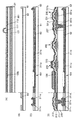
- FIG. 10 is a cross-sectional view illustrating an example of a method for manufacturing a display device.
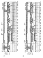
- FIG. 10 is a cross-sectional view illustrating an example of a method for manufacturing a display device.
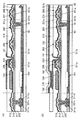
- FIG. 10 is a cross-sectional view illustrating an example of a method for manufacturing a display device.
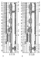
- FIG. 10 is a cross-sectional view illustrating an example of a method for manufacturing a display device.
- FIG. 10 is a cross-sectional view illustrating an example of a method for manufacturing a display device.
- FIG. 10 is a cross-sectional view illustrating an example of a method for manufacturing a display device.
- FIG. 10 is a cross-sectional view illustrating an example of a method for manufacturing a display device.
- FIG. 10 is a cross-sectional view illustrating an example of a method for manufacturing a display device.
- FIG. 10 is a cross-sectional view illustrating an example of a method for manufacturing a display device.
- FIG. 10 is a cross-sectional view illustrating an example of a method for manufacturing a display device.
- FIG. 10 is a cross-sectional view illustrating an example of a method for manufacturing a display device.
- FIG. 10 is a cross-sectional view illustrating an example of a method for manufacturing a display device.
- FIG. 10 is a cross-sectional view illustrating an example of a method for manufacturing a display device.
- FIG. 10 is a cross-sectional view illustrating an example of a method for manufacturing a display device.
- FIG. 10 is a cross-sectional view illustrating an example of a method for manufacturing a display device.
- Sectional drawing which shows an example of a display device and an example of the manufacturing method of a display device.
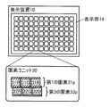
- FIG. 11 is a block diagram illustrating an example of a display device. The figure which shows an example of a pixel unit.
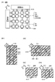
- FIG. 10 illustrates an example of a display device and an example of a pixel.
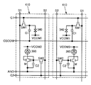
- FIG. 10 is a circuit diagram illustrating an example of a pixel circuit of a display device.
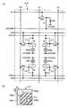
- FIG. 6 is a circuit diagram illustrating an example of a pixel circuit of a display device, and a diagram illustrating an example of a pixel.
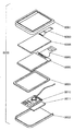
- FIG. 14 illustrates an example of an electronic device.
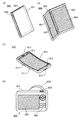
- FIG. 14 illustrates an example of an electronic device.
- FIG. 10 is a cross-sectional view illustrating an example of a method for manufacturing a display device.
- FIG. 10 is a cross-sectional view illustrating an example of a method for manufacturing a display device.
- FIG. 10 is a cross-sectional view illustrating an example of a method for manufacturing a display device.
- FIG. 10 is a cross-sectional view illustrating an example of a method for manufacturing a display device.
- FIG. 10 is a cross-sectional view illustrating an example of a method for manufacturing a display device.
- FIG. 10 is a cross-sectional view illustrating an example of a method for manufacturing a display device.
- FIG. 10 is a cross-sectional view illustrating an example of a display device and an example of a method for manufacturing the display device.
- film and “layer” can be interchanged with each other depending on circumstances or circumstances.
- conductive layer can be changed to the term “conductive film”.
- insulating film can be changed to the term “insulating layer”.
- a metal oxide is a metal oxide in a broad expression.
- Metal oxides are classified into oxide insulators, oxide conductors (including transparent oxide conductors), oxide semiconductors (also referred to as oxide semiconductors or simply OS), and the like.
- oxide semiconductors also referred to as oxide semiconductors or simply OS
- the metal oxide may be referred to as an oxide semiconductor. That is, in the case of describing as an OS FET, it can be said to be a transistor including a metal oxide or an oxide semiconductor.
- metal oxides containing nitrogen may be collectively referred to as metal oxides.
- a metal oxide containing nitrogen may be referred to as a metal oxynitride.
- CAAC c-axis aligned crystal
- CAC Cloud-aligned Composite
- An oxide semiconductor formed by a sputtering method with a substrate temperature of 100 ° C. to 130 ° C. using the target is referred to as sIGZO, and the substrate temperature is set to room temperature (RT) using the target.
- An oxide semiconductor formed by the method is referred to as tIGZO.
- sIGZO has a crystal structure of one or both of nc (nano crystal) and CAAC.
- TIGZO has an nc crystal structure. Note that the room temperature (RT) here includes a temperature when the substrate is not intentionally heated.
- a CAC-OS or a CAC-metal oxide has a function of a conductor in part of a material and a function of a dielectric (or insulator) in part of the material. As a whole, it has a function as a semiconductor. Note that in the case where CAC-OS or CAC-metal oxide is used for a semiconductor layer of a transistor, the conductor has a function of flowing electrons (or holes) serving as carriers, and the dielectric does not flow electrons serving as carriers. It has a function.
- a switching function (function to turn on / off) can be given to the CAC-OS or CAC-metal oxide.
- CAC-OS or CAC-metal oxide by separating each function, both functions can be maximized.
- a CAC-OS or a CAC-metal oxide includes a conductor region and a dielectric region.
- the conductor region has the above-described conductor function
- the dielectric region has the above-described dielectric function.
- the conductor region and the dielectric region may be separated at the nanoparticle level.
- the conductor region and the dielectric region may be unevenly distributed in the material, respectively.
- the conductor region may be observed with the periphery blurred and connected in a cloud shape.
- CAC-OS or CAC-metal oxide can also be called a matrix composite material (metal matrix composite) or a metal matrix composite material (metal matrix composite).
- the conductor region and the dielectric region are dispersed in the material with a size of 0.5 nm to 10 nm, preferably 0.5 nm to 3 nm, respectively. There is.
- the display device of this embodiment includes a first display element that reflects visible light and a second display element that emits visible light.
- the display device of this embodiment has a function of displaying an image using one or both of light reflected by the first display element and light emitted by the second display element.
- the first display element an element that reflects external light for display can be used. Since such an element does not have a light source, power consumption during display can be extremely reduced.
- a reflective liquid crystal element can be typically used.
- a first display element in addition to a shutter type MEMS (Micro Electro Mechanical System) element, an optical interference type MEMS element, a microcapsule type, an electrophoretic type, an electrowetting type, an electronic powder fluid (registered trademark) An element to which a method or the like is applied can be used.
- a shutter type MEMS Micro Electro Mechanical System
- an optical interference type MEMS element in addition to a shutter type MEMS (Micro Electro Mechanical System) element, an optical interference type MEMS element, a microcapsule type, an electrophoretic type, an electrowetting type, an electronic powder fluid (registered trademark)
- An element to which a method or the like is applied can be used.
- a light-emitting element is preferably used for the second display element.
- the light emitted from such a display element is not affected by external light in brightness or chromaticity, so that it has high color reproducibility (wide color gamut), high contrast, and vivid display. Can do.
- a self-luminous light emitting element such as an OLED (Organic Light Emitting Diode), an LED (Light Emitting Diode), or a QLED (Quantum-dot Light Emitting Diode) can be used.
- OLED Organic Light Emitting Diode
- LED Light Emitting Diode
- QLED Quadantum-dot Light Emitting Diode
- the display device of the present embodiment includes a first mode for displaying an image using only the first display element, a second mode for displaying an image using only the second display element, and a first mode There is a third mode in which an image is displayed using the display element and the second display element, and these modes can be used by switching automatically or manually.
- the first mode an image is displayed using the first display element and external light. Since the first mode does not require a light source, it is an extremely low power consumption mode. For example, when external light is sufficiently incident on the display device (for example, in a bright environment), display can be performed using light reflected by the first display element. For example, it is effective when the external light is sufficiently strong and the external light is white light or light in the vicinity thereof.
- the first mode is a mode suitable for displaying characters. In the first mode, light that reflects external light is used, so that it is possible to perform display that is kind to the eyes, and there is an effect that the eyes are less tired.
- the second mode is a mode suitable for displaying vivid images (still images and moving images).
- the third mode display is performed using both reflected light from the first display element and light emission from the second display element. While displaying more vividly than in the first mode, it is possible to suppress power consumption as compared with the second mode. For example, it is effective when the illuminance is relatively low, such as under room lighting or in the morning or evening hours, or when the chromaticity of outside light is not white. Further, by using light in which reflected light and light emission are mixed, it is possible to display an image that makes it feel as if you are looking at a painting.
- FIG. 1 shows a cross-sectional view of the display device 10.
- the display device 10 includes a liquid crystal element 180 as a first display element and a light emitting element 170 as a second display element.
- a display device 10 illustrated in FIG. 1 includes a liquid crystal element 180, a light-emitting element 170, a transistor 41, a transistor 42, and the like between a pair of substrates (a substrate 351 and a substrate 361).
- the liquid crystal element 180 includes an electrode 311 having a function of reflecting visible light, a liquid crystal 112, and an electrode 113 having a function of transmitting visible light.
- the liquid crystal 112 is located between the electrode 311 and the electrode 113.
- the liquid crystal element 180 has a function of reflecting visible light.
- the liquid crystal element 180 emits the reflected light 22 to the substrate 361 side.
- the electrode 311 is electrically connected to the source or drain of the transistor 41 through an opening provided in the insulating layer 220.
- the electrode 311 has a function as a pixel electrode.
- the electrode 113 is electrically connected to the conductive layer 235 through the connection body 243.
- the electrode 311 and the conductive layer 235 can be obtained by processing the same conductive film.
- the light-emitting element 170 includes an electrode 191, an EL layer 192, and an electrode 193.
- the EL layer 192 is located between the electrode 191 and the electrode 193.
- the EL layer 192 includes at least a light-emitting substance.
- the electrode 191 has a function of transmitting visible light.
- the electrode 193 preferably has a function of reflecting visible light.
- the light-emitting element 170 has a function of emitting visible light.
- the light-emitting element 170 is an electroluminescent element that emits light (light emission 21) to the substrate 361 side by applying a voltage between the electrode 191 and the electrode 193.
- the electrode 191 is electrically connected to the source or drain of the transistor 42 through an opening provided in the insulating layer 214.
- the electrode 191 has a function as a pixel electrode.
- An end portion of the electrode 191 is covered with an insulating layer 216.
- the light emitting element 170 is preferably covered with an insulating layer 194.
- the insulating layer 194 is provided in contact with the electrode 193.
- impurities can be prevented from entering the light-emitting element 170, and the reliability of the light-emitting element 170 can be improved.
- a substrate 351 is attached to the insulating layer 194 with an adhesive layer 142.
- the transistor 41 and the transistor 42 are located on the same plane.
- the transistor 41 has a function of controlling driving of the liquid crystal element 180.
- the transistor 42 has a function of controlling driving of the light-emitting element 170.
- the circuit electrically connected to the liquid crystal element 180 is preferably formed on the same plane as the circuit electrically connected to the light emitting element 170. Thereby, the thickness of the display device can be reduced as compared with the case where the two circuits are formed on different surfaces. Further, since the two transistors can be manufactured in the same process, the manufacturing process can be simplified as compared with the case where the two transistors are formed over different surfaces.
- the electrode 311 which is a pixel electrode of the liquid crystal element 180 is positioned opposite to the electrode 191 which is a pixel electrode of the light-emitting element 170 with the gate insulating layer included in the transistors 41 and 42 interposed therebetween.
- the liquid crystal element 180 is used in the case where the transistor 41 which includes an oxide semiconductor in the channel formation region and has extremely low off-state current or a memory element which is electrically connected to the transistor 41 is used.
- the gradation can be maintained. That is, display can be maintained even if the frame rate is extremely small.
- the frame rate can be extremely small, and driving with low power consumption can be performed.
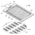
- FIG. 2 is a schematic perspective view of the display device 300.
- the display device 300 has a structure in which a substrate 351 and a substrate 361 are attached to each other.
- the substrate 361 is clearly indicated by a broken line.
- the display device 300 includes a display portion 362, a circuit 364, a wiring 365, and the like.
- FIG. 2 shows an example in which an IC (integrated circuit) 373 and an FPC 372 are mounted on the display device 300. Therefore, the structure illustrated in FIG. 2 can also be referred to as a display module including the display device 300, an IC, and an FPC.
- a scan line driver circuit can be used.
- the wiring 365 has a function of supplying a signal and power to the display portion 362 and the circuit 364.
- the signal and power are input to the wiring 365 from the outside through the FPC 372 or from the IC 373.
- FIG. 2 shows an example in which the IC 373 is provided on the substrate 351 by a COG (Chip On Glass) method, a COF (Chip on Film) method, or the like.
- a COG Chip On Glass
- COF Chip on Film
- an IC having a scan line driver circuit or a signal line driver circuit can be used as the IC 373.
- the display device 300 and the display module may have no IC.
- the IC may be mounted on the FPC by a COF method or the like.
- FIG. 2 shows an enlarged view of a part of the display unit 362.
- electrodes 311b included in the plurality of display elements are arranged in a matrix.
- the electrode 311b has a function of reflecting visible light, and functions as a reflective electrode of the liquid crystal element 180.
- the electrode 311b has an opening 451.
- the display portion 362 includes the light-emitting element 170 on the substrate 351 side of the electrode 311b. Light from the light emitting element 170 is emitted to the substrate 361 side through the opening 451 of the electrode 311b.
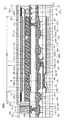
- FIG. 3 illustrates an example of a cross section of the display device 300 illustrated in FIG. 2 when a part of the region including the FPC 372, a part of the region including the circuit 364, and a part of the region including the display portion 362 are cut. Indicates.
- a transistor 3 includes a transistor 201, a transistor 203, a transistor 205, a transistor 206, a liquid crystal element 180, a light-emitting element 170, an insulating layer 220, a colored layer 131, a colored layer 134, and the like between a substrate 351 and a substrate 361.
- a substrate 351 and a substrate 361. Have The substrate 361 and the insulating layer 220 are bonded via an adhesive layer 141. The substrate 351 and the insulating layer 220 are bonded through an adhesive layer 142.
- the substrate 361 is provided with a coloring layer 131, a light shielding layer 132, an insulating layer 121, an electrode 113 functioning as a common electrode of the liquid crystal element 180, an alignment film 133b, an insulating layer 117, and the like.
- a polarizing plate 135 is provided on the outer surface of the substrate 361.
- the insulating layer 121 may function as a planarization layer. Since the surface of the electrode 113 can be substantially flattened by the insulating layer 121, the alignment state of the liquid crystal 112 can be made uniform.
- the insulating layer 117 functions as a spacer for maintaining the cell gap of the liquid crystal element 180.
- the liquid crystal element 180 is a reflective liquid crystal element.
- the liquid crystal element 180 has a stacked structure in which the electrode 311a, the liquid crystal 112, and the electrode 113 are stacked.
- An electrode 311b that reflects visible light is provided in contact with the substrate 351 side of the electrode 311a.
- the electrode 311b has an opening 451.
- the electrode 311a and the electrode 113 transmit visible light.
- An alignment film 133a is provided between the liquid crystal 112 and the electrode 311a.
- An alignment film 133 b is provided between the liquid crystal 112 and the electrode 113.
- the electrode 311b has a function of reflecting visible light
- the electrode 113 has a function of transmitting visible light.
- Light incident from the substrate 361 side is polarized by the polarizing plate 135, passes through the electrode 113, the liquid crystal 112, and the electrode 311a, and is reflected by the electrode 311b.
- the light passes through the electrode 311a, the liquid crystal 112, and the electrode 113 again and reaches the polarizing plate 135.
- the alignment of the liquid crystal can be controlled by the voltage applied between the electrode 311b and the electrode 113, and the optical modulation of light can be controlled. That is, the intensity of light emitted through the polarizing plate 135 can be controlled.
- the light other than the specific wavelength region is absorbed by the colored layer 131, so that the extracted light becomes light exhibiting a desired color, for example, red.
- the resin layer 62a and the insulating layer 63 do not exist between the electrode 311a formed in the display portion 362 and the liquid crystal 112, the influence of light refraction and coloring of the resin layer 62a or the insulating layer 63 is reduced.
- the electrode 311a and the electrode 311b are formed to cover the recesses provided in the resin layer 62 and the insulating layer 63 in the same manner as the conductive layer 311c, the conductive layer 311d, the conductive layer 311e, and the conductive layer 311f.
- the insulating layer 63 can be easily removed.
- the opening 451 is preferably provided with an electrode 311a that transmits visible light. Accordingly, since the liquid crystal 112 is aligned in the region overlapping with the opening 451 as well as the other regions, it is possible to suppress the occurrence of unintended light leakage due to the alignment failure of the liquid crystal at the boundary between these regions.
- connection portion 207 the electrode 311b is electrically connected to the conductive layer 222a included in the transistor 206 through the conductive layer 221b.
- the transistor 206 has a function of controlling driving of the liquid crystal element 180.
- connection portion 252 is provided in a part of the region where the adhesive layer 141 is provided.
- the conductive layer 311 e obtained by processing the same conductive film as the electrode 311 a and a part of the electrode 113 are electrically connected to each other through the connection body 243. Therefore, a signal or a potential input from the FPC 372 connected to the substrate 351 side can be supplied to the electrode 113 formed on the substrate 361 side through the connection portion 252.
- connection portion 252 covers the concave portions provided in the resin layer 62a and the insulating layer 63, and forms the conductive layer 311e and the conductive layer 311f with the same material as the electrode 311a and the electrode 311b.
- the conductive layer 311e exposed from the connection body 243 Is touching by the surface.
- connection body 243 for example, conductive particles can be used.
- conductive particles those obtained by coating the surface of particles such as organic resin or silica with a metal material can be used. It is preferable to use nickel or gold as the metal material because the contact resistance can be reduced. In addition, it is preferable to use particles in which two or more kinds of metal materials are coated in layers, such as further coating nickel with gold. Further, it is preferable to use a material that is elastically deformed or plastically deformed as the connection body 243.
- the connection body 243 which is a conductive particle, may have a shape crushed in the vertical direction as shown in FIG. By doing so, the contact area between the connection body 243 and the conductive layer electrically connected to the connection body 243 can be increased, the contact resistance can be reduced, and the occurrence of problems such as connection failure can be suppressed.
- connection body 243 is preferably disposed so as to be covered with the adhesive layer 141.
- connection body 243 may be dispersed in the adhesive layer 141 before curing.
- the light emitting element 170 is a bottom emission type light emitting element.
- the light-emitting element 170 has a stacked structure in which the electrode 191, the EL layer 192, and the electrode 193 are stacked in this order from the insulating layer 220 side.
- the electrode 191 is connected to the conductive layer 222 b included in the transistor 205 through an opening provided in the insulating layer 214.
- the transistor 205 has a function of controlling driving of the light-emitting element 170.
- An insulating layer 216 covers the end portion of the electrode 191.
- the electrode 193 includes a material that reflects visible light, and the electrode 191 includes a material that transmits visible light.
- An insulating layer 194 is provided to cover the electrode 193. Light emitted from the light-emitting element 170 is emitted to the substrate 361 side through the coloring layer 134, the insulating layer 220, the opening 451, the electrode 311a, and the like.
- the liquid crystal element 180 and the light emitting element 170 can exhibit various colors by changing the color of the colored layer depending on the pixel.
- the display device 300 can perform color display using the liquid crystal element 180.
- the display device 300 can perform color display using the light-emitting element 170.
- the transistors 201, 203, 205, and 206 are all formed on the surface of the insulating layer 220 on the substrate 351 side. These transistors can be manufactured using the same process.
- the transistor 203 is a transistor (also referred to as a switching transistor or a selection transistor) that controls pixel selection / non-selection.
- the transistor 205 is a transistor (also referred to as a drive transistor) that controls a current flowing through the light-emitting element 170.
- Insulating layers such as an insulating layer 211, an insulating layer 212, an insulating layer 213, and an insulating layer 214 are provided on the substrate 351 side of the insulating layer 220.
- a part of the insulating layer 211 functions as a gate insulating layer of each transistor.
- the insulating layer 212 is provided so as to cover the transistor 206 and the like.
- the insulating layer 213 is provided so as to cover the transistor 205 and the like.
- the insulating layer 214 functions as a planarization layer. Note that the number of insulating layers covering the transistor is not limited, and may be a single layer or two or more layers.
- the insulating layer can function as a barrier film.
- impurities can be effectively prevented from diffusing from the outside with respect to the transistor, and a highly reliable display device can be realized.
- the transistor 201, the transistor 203, the transistor 205, and the transistor 206 include a part of the conductive layer 221a that functions as a gate, a part of the insulating layer 211 that functions as a gate insulating layer, a conductive layer 222a and a conductive layer that function as a source and a drain. 222 b and the semiconductor layer 231.
- the same hatching pattern is given to a plurality of layers obtained by processing the same conductive film.
- the transistor 201 and the transistor 205 include a conductive layer 223 that functions as a gate.
- a structure in which a semiconductor layer in which a channel is formed is sandwiched between two gates is applied to the transistor 201 and the transistor 205.
- the transistor may be driven by connecting two gates and supplying the same signal thereto.
- Such a transistor can have higher field-effect mobility than other transistors, and can increase on-state current.
- a circuit that can be driven at high speed can be manufactured.
- the area occupied by the circuit portion can be reduced.
- the threshold voltage of the transistor can be controlled by applying a potential for controlling the threshold voltage to one of the two gates and applying a potential for driving to the other of the two gates.
- the transistor included in the circuit 364 and the transistor included in the display portion 362 may have the same structure or different structures.
- the plurality of transistors included in the circuit 364 may have the same structure, or two or more structures may be used in combination.
- the plurality of transistors included in the display portion 362 may have the same structure, or two or more structures may be used in combination.
- a conductive material containing an oxide is preferably used for the conductive layer 223.
- oxygen can be supplied to the insulating layer 212 by being formed in an atmosphere containing oxygen.
- the proportion of oxygen gas in the film forming gas is preferably in the range of 90% to 100%.
- Oxygen supplied to the insulating layer 212 is supplied to the semiconductor layer 231 by a later heat treatment, so that oxygen vacancies in the semiconductor layer 231 can be reduced.
- the conductive layer 223 is preferably formed using a low-resistance oxide semiconductor.
- an insulating film from which hydrogen is released for example, a silicon nitride film or the like is preferably used for the insulating layer 213. Hydrogen is supplied into the conductive layer 223 during the formation of the insulating layer 213 or by a subsequent heat treatment, so that the electrical resistance of the conductive layer 223 can be effectively reduced.
- a colored layer 134 is provided in contact with the insulating layer 213.
- the colored layer 134 is covered with the insulating layer 214.
- connection portion 204 is provided in a region of the substrate 351 that does not overlap with the substrate 361.
- the wiring 365 is electrically connected to the FPC 372 through the connection layer 242.
- a conductive layer 311c and a conductive layer 311d are formed of the same material as the electrodes 311a and 311b so as to cover the concave portions provided in the resin layer 62a and the insulating layer 63 in the connection portion 204.
- the conductive layer 311c is exposed. Accordingly, the connection unit 204 and the FPC 372 can be electrically connected via the connection layer 242.
- the conductive layer 311c and the conductive layer 311d are formed so as to cover the recesses provided in the resin layer 62a and the insulating layer 63, the conductive layer 311c can be easily exposed on the upper surface of the connection portion 204.
- a linear polarizing plate may be used as the polarizing plate 135 disposed on the outer surface of the substrate 361, but a circular polarizing plate may also be used.
- a circularly-polarizing plate what laminated
- a desired contrast may be realized by adjusting a cell gap, an alignment, a driving voltage, and the like of the liquid crystal element used for the liquid crystal element 180 in accordance with the type of the polarizing plate.
- optical members can be arranged outside the substrate 361.
- the optical member include a polarizing plate, a retardation plate, a light diffusion layer (such as a diffusion film), an antireflection layer, and a light collecting film.
- a polarizing plate such as a retardation plate
- a light diffusion layer such as a diffusion film
- an antireflection layer such as a diffusion film
- a light collecting film such as a light collecting film.
- an antistatic film that suppresses adhesion of dust a water-repellent film that makes it difficult to adhere dirt, a hard coat film that suppresses generation of scratches due to use, and the like may be arranged.
- the substrate 351 and the substrate 36 glass, quartz, ceramic, sapphire, organic resin, or the like can be used, respectively.
- a flexible material is used for the substrate 351 and the substrate 361, the flexibility of the display device can be increased.
- liquid crystal element 180 for example, a liquid crystal element to which a vertical alignment (VA) mode is applied can be used.
- VA vertical alignment
- MVA Multi-Domain Vertical Alignment
- PVA Plasma Vertical Alignment
- ASV Advanced Super View
- liquid crystal elements to which various modes are applied can be used.
- VA mode Transmission Nematic
- IPS In-Plane-Switching
- FFS Ringe Field Switching
- ASM Analy Symmetrical Aligned Micro-cell
- FLC Ferroelectric Liquid Crystal
- AFLC Antiferroelectric Liquid Crystal
- the liquid crystal element is an element that controls transmission or non-transmission of light by an optical modulation action of liquid crystal.
- the optical modulation action of the liquid crystal is controlled by an electric field applied to the liquid crystal (including a horizontal electric field, a vertical electric field, or an oblique electric field).
- a thermotropic liquid crystal a low molecular liquid crystal, a polymer liquid crystal, a polymer dispersed liquid crystal (PDLC), a ferroelectric liquid crystal, an antiferroelectric liquid crystal, or the like can be used.
- PDLC polymer dispersed liquid crystal
- ferroelectric liquid crystal an antiferroelectric liquid crystal, or the like
- These liquid crystal materials exhibit a cholesteric phase, a smectic phase, a cubic phase, a chiral nematic phase, an isotropic phase, and the like depending on conditions.
- liquid crystal material either a positive type liquid crystal or a negative type liquid crystal may be used, and an optimal liquid crystal material may be used according to an applied mode or design.
- an alignment film can be provided.
- liquid crystal exhibiting a blue phase for which an alignment film is unnecessary may be used.
- the blue phase is one of the liquid crystal phases.
- a liquid crystal composition mixed with several percent by weight or more of a chiral agent is used for the liquid crystal in order to improve the temperature range.
- a liquid crystal composition containing a liquid crystal exhibiting a blue phase and a chiral agent has a short response speed and is optically isotropic.
- a liquid crystal composition including a liquid crystal exhibiting a blue phase and a chiral agent does not require alignment treatment and has a small viewing angle dependency. Further, since it is not necessary to provide an alignment film, a rubbing process is not required, so that electrostatic breakdown caused by the rubbing process can be prevented, and defects or breakage of the liquid crystal display device during the manufacturing process can be reduced. .
- a polarizing plate 135 is provided on the display surface side. Separately from this, it is preferable to arrange a light diffusing plate on the display surface side because the visibility can be improved.
- a front light may be provided outside the polarizing plate 135.
- an edge light type front light is preferably used. It is preferable to use a front light including an LED (Light Emitting Diode) because power consumption can be reduced.
- LED Light Emitting Diode
- various curable adhesives such as an ultraviolet curable photocurable adhesive, a reactive curable adhesive, a thermosetting adhesive, and an anaerobic adhesive can be used.
- these adhesives include epoxy resins, acrylic resins, silicone resins, phenol resins, polyimide resins, imide resins, PVC (polyvinyl chloride) resins, PVB (polyvinyl butyral) resins, EVA (ethylene vinyl acetate) resins, and the like.
- a material with low moisture permeability such as an epoxy resin is preferable.
- a two-component mixed resin may be used.
- an adhesive sheet or the like may be used.
- connection layer 242 an anisotropic conductive film (ACF: Anisotropic Conductive Film), an anisotropic conductive paste (ACP: Anisotropic Conductive Paste), or the like can be used.
- ACF Anisotropic Conductive Film
- ACP Anisotropic Conductive Paste
- the light emitting element 170 includes a top emission type, a bottom emission type, a dual emission type, and the like.
- a conductive film that transmits visible light is used for the electrode from which light is extracted.
- a conductive film that reflects visible light is preferably used for the electrode from which light is not extracted.
- the EL layer 192 includes at least a light-emitting layer.
- the EL layer 192 is a layer other than the light-emitting layer and is a substance having a high hole-injecting property, a substance having a high hole-transporting property, a hole blocking material, a substance having a high electron-transporting property, a substance having a high electron-injecting property, or a bipolar property
- a layer containing a substance (a substance having a high electron transporting property and a high hole transporting property) or the like may be further included.
- the EL layer 192 either a low molecular compound or a high molecular compound can be used, and an inorganic compound may be included.
- the layers constituting the EL layer 192 can be formed by a method such as a vapor deposition method (including a vacuum vapor deposition method), a transfer method, a printing method, an ink jet method, or a coating method.
- the EL layer 192 may include an inorganic compound such as a quantum dot.
- a quantum dot can be used for a light emitting layer to function as a light emitting material.
- a quantum dot material a colloidal quantum dot material, an alloy type quantum dot material, a core / shell type quantum dot material, a core type quantum dot material, or the like can be used.
- a material including an element group of Group 12 and Group 16, Group 13 and Group 15, or Group 14 and Group 16 may be used.
- a quantum dot material containing an element such as cadmium, selenium, zinc, sulfur, phosphorus, indium, tellurium, lead, gallium, arsenic, or aluminum may be used.
- light with high color purity can be extracted from the display device by applying a combination of a color filter (colored layer) and a microcavity structure (optical adjustment layer).
- the film thickness of the optical adjustment layer is changed according to the color of each pixel.
- materials that can be used for conductive layers such as various wirings and electrodes constituting the display device include aluminum, titanium, chromium, nickel, copper, yttrium, zirconium, molybdenum, silver, A metal such as tantalum or tungsten, or an alloy containing the same as a main component can be given. A film containing any of these materials can be used as a single layer or a stacked structure.
- conductive oxide such as indium oxide, indium tin oxide, indium zinc oxide, zinc oxide, or zinc oxide to which gallium is added, or graphene
- a metal material such as gold, silver, platinum, magnesium, nickel, tungsten, chromium, molybdenum, iron, cobalt, copper, palladium, or titanium, or an alloy material containing the metal material
- a nitride eg, titanium nitride
- a metal material or an alloy material (or a nitride thereof) it may be thin enough to have a light-transmitting property.
- a stacked film of the above materials can be used as a conductive layer.
- a laminated film of an alloy of silver and magnesium and indium tin oxide because the conductivity can be increased.
- conductive layers such as various wirings and electrodes constituting the display device and conductive layers (conductive layers functioning as pixel electrodes and common electrodes) included in the display element.
- Examples of the insulating material that can be used for each insulating layer include inorganic insulating materials such as resins such as acrylic and epoxy, silicon oxide, silicon oxynitride, silicon nitride oxide, silicon nitride, and aluminum oxide.
- inorganic insulating materials such as resins such as acrylic and epoxy, silicon oxide, silicon oxynitride, silicon nitride oxide, silicon nitride, and aluminum oxide.
- Examples of materials that can be used for the colored layer include metal materials, resin materials, resin materials containing pigments or dyes, and the like.
- a display device 300A illustrated in FIG. 4 is mainly different from the display device 300 in that it does not include the transistor 201, the transistor 203, the transistor 205, and the transistor 206 but includes the transistor 281, the transistor 284, the transistor 285, and the transistor 286. .
- two transistors included in the display device may be partially stacked. Thereby, since the area occupied by the pixel circuit can be reduced, the definition can be increased. In addition, the light emitting area of the light emitting element 170 can be increased and the aperture ratio can be improved. If the light-emitting element 170 has a high aperture ratio, the current density for obtaining necessary luminance can be reduced, so that reliability is improved.
- the transistor 281, the transistor 284, and the transistor 286 each include a conductive layer 221a, an insulating layer 211, a semiconductor layer 231, a conductive layer 222a, and a conductive layer 222b.
- the conductive layer 221a overlaps with the semiconductor layer 231 with the insulating layer 211 interposed therebetween.
- the conductive layer 222 a and the conductive layer 222 b are electrically connected to the semiconductor layer 231.
- the transistor 281 includes a conductive layer 223.
- the transistor 285 includes a conductive layer 222b, an insulating layer 217, a semiconductor layer 261, a conductive layer 223, an insulating layer 212, an insulating layer 213, a conductive layer 263a, and a conductive layer 263b.
- the conductive layer 222b overlaps with the semiconductor layer 261 with the insulating layer 217 interposed therebetween.
- the conductive layer 223 overlaps with the semiconductor layer 261 with the insulating layer 212 and the insulating layer 213 interposed therebetween.
- the conductive layer 263a and the conductive layer 263b are electrically connected to the semiconductor layer 261.
- the conductive layer 221a functions as a gate.
- the insulating layer 211 functions as a gate insulating layer.
- the conductive layer 222a functions as one of a source and a drain.
- the conductive layer 222b included in the transistor 286 functions as the other of the source and the drain.
- the conductive layer 222b shared by the transistor 284 and the transistor 285 includes a portion functioning as the other of the source and the drain of the transistor 284 and a portion functioning as the gate of the transistor 285.
- the insulating layer 217, the insulating layer 212, and the insulating layer 213 function as gate insulating layers.
- One of the conductive layer 263a and the conductive layer 263b functions as a source, and the other functions as a drain.
- the conductive layer 223 functions as a gate.
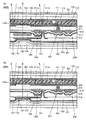
- FIG. 5A is a cross-sectional view of a display portion of the display device 300B.
- the display device 300B is different from the display device 300 in that the display device 300B does not include the colored layer 131. Since other configurations are the same as those of the display device 300, detailed description thereof is omitted.
- the liquid crystal element 180 exhibits white. Since the colored layer 131 is not included, the display device 300 can perform display in black and white or gray scale using the liquid crystal element 180.
- a display device 300C illustrated in FIG. 5B is different from the display device 300B in that the EL layer 192 is separately applied and the coloring layer 134 is not provided. Since other configurations are the same as those of the display device 300B, detailed description thereof is omitted.
- the light-emitting element 170 to which the separate coating method is applied it is sufficient that at least one layer (typically, the light-emitting layer) of the EL layer 192 is coated, and all the layers constituting the EL layer are coated. It may be divided.
- the structure of the transistor included in the display device is not particularly limited.
- a planar transistor, a staggered transistor, or an inverted staggered transistor may be used.
- any transistor structure of a top gate structure or a bottom gate structure may be employed.
- gate electrodes may be provided above and below the channel.
- 6A to 6E illustrate structural examples of transistors.
- a transistor 110a illustrated in FIG. 6A is a top-gate transistor.
- the transistor 110a includes a conductive layer 221, an insulating layer 211, a semiconductor layer 231, an insulating layer 212, a conductive layer 222a, and a conductive layer 222b.
- the semiconductor layer 231 is provided over the insulating layer 151.
- the conductive layer 221 overlaps with the semiconductor layer 231 with the insulating layer 211 interposed therebetween.
- the conductive layers 222 a and 222 b are electrically connected to the semiconductor layer 231 through openings provided in the insulating layers 211 and 212.
- the conductive layer 221 functions as a gate.
- the insulating layer 211 functions as a gate insulating layer.
- One of the conductive layer 222a and the conductive layer 222b functions as a source, and the other functions as a drain.
- the physical distance between the conductive layer 221 and the conductive layer 222a or the conductive layer 222b can be easily increased, so that the parasitic capacitance between them can be reduced.
- a transistor 110b illustrated in FIG. 6B includes a conductive layer 223 and an insulating layer 218 in addition to the structure of the transistor 110a.
- the conductive layer 223 is provided over the insulating layer 151 and overlaps with the semiconductor layer 231.
- the insulating layer 218 is provided so as to cover the conductive layer 223 and the insulating layer 151.
- the conductive layer 223 functions as one of a pair of gates. Therefore, the on-state current of the transistor can be increased, the threshold voltage can be controlled, and the like.
- FIGS. 6C to 6E show examples of structures in which two transistors are stacked.
- the structures of the two stacked transistors can be determined independently, and are not limited to the combinations of FIGS.
- FIG. 6C illustrates a structure in which the transistor 110c and the transistor 110d are stacked.
- the transistor 110c has two gates.
- the transistor 110d has a bottom gate structure. Note that the transistor 110c may include one gate (top gate structure).
- the transistor 110d may have two gates.
- the transistor 110c includes a conductive layer 223, an insulating layer 218, a semiconductor layer 231, a conductive layer 221, an insulating layer 211, a conductive layer 222a, and a conductive layer 222b.
- the conductive layer 223 is provided over the insulating layer 151.
- the conductive layer 223 overlaps with the semiconductor layer 231 with the insulating layer 218 interposed therebetween.
- the insulating layer 218 is provided so as to cover the conductive layer 223 and the insulating layer 151.
- the conductive layer 221 overlaps with the semiconductor layer 231 with the insulating layer 211 interposed therebetween.
- FIG. 6C illustrates an example in which the insulating layer 211 is provided only in a portion overlapping with the conductive layer 221, but the insulating layer 211 covers an end portion of the semiconductor layer 231 as illustrated in FIG. 6B and the like. It may be provided as follows.
- the conductive layer 222 a and the conductive layer 222 b are electrically connected to the semiconductor layer 231 through an opening provided in the insulating layer 212.
- the transistor 110d includes a conductive layer 222b, an insulating layer 213, a semiconductor layer 261, a conductive layer 263a, and a conductive layer 263b.
- the conductive layer 222 b includes a region overlapping with the semiconductor layer 261 with the insulating layer 213 interposed therebetween.
- the insulating layer 213 is provided so as to cover the conductive layer 222b.
- the conductive layer 263a and the conductive layer 263b are electrically connected to the semiconductor layer 261.
- the conductive layer 221 and the conductive layer 223 each function as a gate of the transistor 110c.
- the insulating layer 218 and the insulating layer 211 function as a gate insulating layer of the transistor 110c.
- the conductive layer 222a functions as one of a source and a drain of the transistor 110c.
- the conductive layer 222b includes a portion functioning as the other of the source and the drain of the transistor 110c and a portion functioning as the gate of the transistor 110d.
- the insulating layer 213 functions as a gate insulating layer of the transistor 110d.
- One of the conductive layer 263a and the conductive layer 263b functions as a source of the transistor 110d, and the other functions as a drain of the transistor 110d.
- the transistors 110c and 110d are preferably applied to the pixel circuit of the light-emitting element 170.
- the transistor 110c can be used as a selection transistor
- the transistor 110d can be used as a driving transistor.
- the conductive layer 263b is electrically connected to an electrode 191 functioning as a pixel electrode of the light-emitting element through an opening provided in the insulating layer 217 and the insulating layer 214.
- FIG. 6D illustrates a structure in which the transistor 110e and the transistor 110f are stacked.
- the transistor 110e has a bottom gate structure.
- the transistor 110f has two gates.
- the transistor 110e may have two gates.
- the transistor 110e includes a conductive layer 221, an insulating layer 211, a semiconductor layer 231, a conductive layer 222a, and a conductive layer 222b.
- the conductive layer 221 is provided over the insulating layer 151.
- the conductive layer 221 overlaps with the semiconductor layer 231 with the insulating layer 211 interposed therebetween.
- the insulating layer 211 is provided to cover the conductive layer 221 and the insulating layer 151.
- the conductive layer 222 a and the conductive layer 222 b are electrically connected to the semiconductor layer 231.
- the transistor 110f includes a conductive layer 222b, an insulating layer 212, a semiconductor layer 261, a conductive layer 223, an insulating layer 218, an insulating layer 213, a conductive layer 263a, and a conductive layer 263b.
- the conductive layer 222 b includes a region overlapping with the semiconductor layer 261 with the insulating layer 212 interposed therebetween.
- the insulating layer 212 is provided so as to cover the conductive layer 222b.
- the conductive layers 263 a and 263 b are electrically connected to the semiconductor layer 261 through openings provided in the insulating layer 213.
- the conductive layer 223 overlaps with the semiconductor layer 261 with the insulating layer 218 provided therebetween.
- the insulating layer 218 is provided in a portion overlapping with the conductive layer 223.
- the conductive layer 221 functions as the gate of the transistor 110e.
- the insulating layer 211 functions as a gate insulating layer of the transistor 110e.
- the conductive layer 222a functions as one of a source and a drain of the transistor 110e.
- the conductive layer 222b includes a portion functioning as the other of the source and the drain of the transistor 110e and a portion functioning as the gate of the transistor 110f.
- the conductive layer 223 functions as the gate of the transistor 110f.
- the insulating layer 212 and the insulating layer 218 each function as a gate insulating layer of the transistor 110f.
- One of the conductive layer 263a and the conductive layer 263b functions as a source of the transistor 110f, and the other functions as a drain of the transistor 110f.
- the conductive layer 263b is electrically connected to an electrode 191 functioning as a pixel electrode of the light-emitting element through an opening provided in the insulating layer 214.
- FIG. 6E illustrates a structure in which the transistor 110g and the transistor 110h are stacked.
- the transistor 110g has a top gate structure.
- the transistor 110h has two gates. Note that the transistor 110g may include two gates.
- the transistor 110g includes a semiconductor layer 231, a conductive layer 221, an insulating layer 211, a conductive layer 222a, and a conductive layer 222b.
- the semiconductor layer 231 is provided over the insulating layer 151.
- the conductive layer 221 overlaps with the semiconductor layer 231 with the insulating layer 211 interposed therebetween.
- the insulating layer 211 is provided so as to overlap with the conductive layer 221.
- the conductive layer 222 a and the conductive layer 222 b are electrically connected to the semiconductor layer 231 through an opening provided in the insulating layer 212.
- the transistor 110h includes a conductive layer 222b, an insulating layer 213, a semiconductor layer 261, a conductive layer 223, an insulating layer 218, an insulating layer 217, a conductive layer 263a, and a conductive layer 263b.
- the conductive layer 222 b includes a region overlapping with the semiconductor layer 261 with the insulating layer 213 interposed therebetween.
- the insulating layer 213 is provided so as to cover the conductive layer 222b.
- the conductive layers 263 a and 263 b are electrically connected to the semiconductor layer 261 through openings provided in the insulating layer 217.
- the conductive layer 223 overlaps with the semiconductor layer 261 with the insulating layer 218 provided therebetween.
- the insulating layer 218 is provided in a portion overlapping with the conductive layer 223.
- the conductive layer 221 functions as the gate of the transistor 110g.
- the insulating layer 211 functions as a gate insulating layer of the transistor 110g.
- the conductive layer 222a functions as one of a source and a drain of the transistor 110g.
- the conductive layer 222b includes a portion functioning as the other of the source and the drain of the transistor 110g and a portion functioning as the gate of the transistor 110h.
- the conductive layer 223 functions as the gate of the transistor 110h.
- the insulating layer 213 and the insulating layer 218 each function as a gate insulating layer of the transistor 110h.
- One of the conductive layer 263a and the conductive layer 263b functions as a source of the transistor 110h, and the other functions as a drain of the transistor 110h.
- the conductive layer 263b is electrically connected to an electrode 191 functioning as a pixel electrode of the light-emitting element through an opening provided in the insulating layer 214.
- a thin film (an insulating film, a semiconductor film, a conductive film, or the like) included in the display device is formed by a sputtering method, a chemical vapor deposition (CVD) method, a vacuum evaporation method, or a pulse laser deposition (PLD: Pulse Laser Deposition).
- CVD chemical vapor deposition
- PLD Pulse Laser Deposition
- ALD Atomic Layer Deposition
- the CVD method may be a plasma enhanced chemical vapor deposition (PECVD) method or a thermal CVD method.
- PECVD plasma enhanced chemical vapor deposition
- MOCVD metal organic chemical vapor deposition
- Thin films (insulating films, semiconductor films, conductive films, etc.) that constitute display devices are spin coat, dip, spray coating, ink jet, dispense, screen printing, offset printing, doctor knife, slit coat, roll coat, curtain coat. It can be formed by a method such as knife coating.
- the thin film can be processed using a lithography method or the like.
- an island-shaped thin film may be formed by a film formation method using a shielding mask.
- the thin film may be processed by a nanoimprint method, a sand blast method, a lift-off method, or the like.
- a photolithography method a resist mask is formed on a thin film to be processed, the thin film is processed by etching or the like, and the resist mask is removed. After forming a photosensitive thin film, exposure and development are performed. And a method for processing the thin film into a desired shape.
- light used for exposure can be i-line (wavelength 365 nm), g-line (wavelength 436 nm), h-line (wavelength 405 nm), or light in which these are mixed.
- ultraviolet light, KrF laser light, ArF laser light, or the like can be used.
- exposure may be performed by an immersion exposure technique.
- extreme ultraviolet light (EUV: Extreme-violet) or X-rays may be used as light used for exposure.
- an electron beam can be used instead of the light used for exposure. It is preferable to use extreme ultraviolet light, X-rays, or an electron beam because extremely fine processing is possible. Note that a photomask is not necessary when exposure is performed by scanning a beam such as an electron beam.
- etching the thin film For etching the thin film, a dry etching method, a wet etching method, a sand blasting method, or the like can be used.
- Example of manufacturing method of display device> an example of a method for manufacturing the display device 300 illustrated in FIG. 3 will be described. 7 to 23, the manufacturing method will be described by paying attention to the display portion 362 and the external connection portion of the display device 300 in particular.
- the colored layer 131 is formed over the substrate 361 (FIG. 7A).
- the colored layer 131 can be processed into an island shape by a photolithography method or the like by being formed using a photosensitive material. Note that in the circuit 364 and the like illustrated in FIG. 3, the light-blocking layer 132 is provided over the substrate 361.
- the insulating layer 121 is formed over the coloring layer 131 and the light shielding layer 132.
- the insulating layer 121 preferably functions as a planarization layer.
- Examples of the insulating layer 121 include acrylic resin, epoxy resin, polyamide resin, polyimide amide resin, siloxane resin, benzocyclobutene resin, and phenol resin.
- An inorganic insulating film may be applied to the insulating layer 121.
- an inorganic insulating film for example, a silicon nitride film, a silicon oxynitride film, a silicon oxide film, a silicon nitride oxide film, an aluminum oxide film, an aluminum nitride film, or the like can be used.
- a hafnium oxide film, an yttrium oxide film, a zirconium oxide film, a gallium oxide film, a tantalum oxide film, a magnesium oxide film, a lanthanum oxide film, a cerium oxide film, a neodymium oxide film, or the like may be used. Two or more of the above insulating films may be stacked.
- the electrode 113 is formed.
- the electrode 113 can be formed by forming a conductive film, forming a resist mask, etching the conductive film, and then removing the resist mask.
- the electrode 113 is formed using a conductive material that transmits visible light.
- the insulating layer 117 is formed over the electrode 113.
- An organic insulating film is preferably used for the insulating layer 117.
- an alignment film 133b is formed over the electrode 113 and the insulating layer 117 (FIG. 7A).
- the alignment film 133b can be formed by performing a rubbing process after forming a thin film such as a resin.
- the first resin layer 62p is formed over the manufacturing substrate 61.
- the first resin layer 62p can be formed using various resin materials (including a resin precursor).
- the various resin materials preferably have thermosetting properties. Further, it may or may not have photosensitivity.
- the concave portion can be formed using a lithography method using light.
- the first resin layer 62p is preferably formed using a material containing a polyimide resin or a polyimide resin precursor.
- the resin material include a material containing a polyimide resin and a solvent, or a material containing a polyamic acid and a solvent. Since polyimide is a material that is suitably used for a planarizing film or the like of a display device, the film forming device and the material can be shared. Therefore, no new device or material is required to realize the structure of one embodiment of the present invention, which is advantageous in terms of cost.
- examples of materials that can be used for forming the first resin layer 62p include acrylic resins, epoxy resins, polyamide resins, polyimide amide resins, siloxane resins, benzocyclobutene resins, phenol resins, and those resins. A precursor etc. are mentioned.
- Examples of the method for forming the first resin layer 62p include spin coating, dip coating, spray coating, ink jet, dispensing, screen printing, offset printing, doctor knife, slit coating, roll coating, curtain coating, and knife coating.
- the first resin layer 62p is preferably formed using a spin coater. By using the spin coating method, a thin film can be uniformly formed on a large substrate.
- a portion corresponding to the connection portion and a part in the thickness direction of the first resin layer 62p of the pixel portion are removed, and the first region is formed in the first resin layer 62p.
- a second region also referred to as a recess
- the resin layer 62 of the pixel portion does not need to have a recess.
- the thickness of the first region of the resin layer 62 may be from 0.1 ⁇ m to less than 20 ⁇ m, preferably from 0.1 ⁇ m to 10 ⁇ m, more preferably from 0.1 ⁇ m to 3 ⁇ m, More preferably, it is 5 ⁇ m or more and 2 ⁇ m or less.
- the thermal expansion coefficient of the resin layer 62 is preferably 0.1 ppm / ° C. or more and 50 ppm / ° C. or less, more preferably 0.1 ppm / ° C. or more and 20 ppm / ° C. or less, and 0.1 ppm / ° C. or more and 10 ppm / ° C. or less. More preferably, it is not higher than ° C. As the coefficient of thermal expansion of the resin layer 62 is lower, it is possible to suppress the generation of cracks in the layer constituting the transistor or the like, or the damage of the transistor or the like due to heating.
- the resin layer 62 When the resin layer 62 remains on the optical path from which light from the display device is emitted, the resin layer 62 preferably has a high light-transmitting property with respect to visible light.
- the second region can be formed by a lithography method using light. Specifically, heat treatment (also referred to as pre-baking treatment) for removing the solvent contained in the first resin layer 62p is performed on the first resin layer 62p, and then exposure is performed using a photomask. Subsequently, unnecessary portions can be removed by performing development processing.
- the resin layer 62 having a concave portion can be formed by reducing the exposure amount as compared with the condition for providing an opening in the resin layer 62. For example, methods such as shortening the exposure time, weakening the light intensity, and shifting the focus of light than the exposure conditions for forming the opening in the resin layer 62 can be mentioned.
- a multi-tone mask may be used.
- the concave portion may be formed by pressing a mold having a desired shape against the formed film.
- the recess can be formed even when the first resin layer 62p is formed of a non-photosensitive material.
- embossing may be performed before the pre-baking process or after the pre-baking process and before the first heat treatment.
- the coverage of the film formed on the concave portion of the resin layer 62 is improved.
- a photosensitive resin a positive type resin is used.
- embossing it is preferable to use a die having a tapered shape.
- the resin layer 62 with the second region having a thickness smaller than that of the first region, and further disposing the conductive layer so as to cover the second region, the conductive layer is exposed in a later step. It becomes easy. Further, even if the resin layer is removed until the conductive layer is exposed, a part of the resin layer remains, so that the remaining resin layer can be used as a protective layer.
- a first heat treatment is performed.
- the first heat treatment is preferably performed in an atmosphere containing oxygen.
- the force required to peel off the resin layer 62 can be reduced.
- the higher the proportion of oxygen in the atmosphere of the first heat treatment the more oxygen can be contained in the resin layer 62, and the peelability of the resin layer 62 can be improved.
- the first heat treatment can be performed, for example, in a state where the inside of the chamber of the heating device is in an atmosphere containing oxygen.
- the first heat treatment can be performed using a hot plate or the like in an air atmosphere.
- the oxygen partial pressure in the atmosphere during the first heat treatment is preferably 5% or more and less than 100%, more preferably 10% or more and less than 100%, and even more preferably 15% or more and less than 100%.
- the first heat treatment is preferably performed while flowing a gas containing oxygen into the chamber of the heating device.
- the first heat treatment is preferably performed, for example, while flowing only oxygen gas or a mixed gas containing oxygen gas.
- a mixed gas containing oxygen and nitrogen or a rare gas such as argon can be used.
- the proportion of the oxygen gas flow rate in the total mixed gas flow rate is preferably 5% to 50%, more preferably 10% to 50%. Preferably, it is more preferably 15% or more and 50% or less.
- the temperature of the first heat treatment is preferably 200 ° C. or higher and 500 ° C. or lower, more preferably 250 ° C. or higher and 475 ° C. or lower, and further preferably 300 ° C. or higher and 450 ° C. or lower.
- the peelability of the resin layer 62 can be improved as the temperature of the first heat treatment is higher.
- degassing components for example, hydrogen, water, etc.
- the film to be the resin layer 62 is preferably heated at 350 ° C. or higher and 450 ° C. or lower, more preferably 400 ° C. or lower, and even more preferably 375 ° C. or lower.
- degassing from the resin layer 62 in the transistor manufacturing process can be significantly suppressed.
- the maximum temperature in manufacturing the transistor be equal to the temperature in the first heat treatment because the highest temperature in manufacturing the display device can be prevented by performing the first heat treatment.
- the peelability of the resin layer 62 can be improved, so that the time of 1st heat processing is long.
- the time for the first heat treatment is, for example, preferably 5 minutes to 24 hours, more preferably 30 minutes to 12 hours, and further preferably 1 hour to 6 hours. Note that the time of the first heat treatment is not limited to this. For example, when the first heat treatment is performed using an RTA (Rapid Thermal Annealing) method, it may be less than 5 minutes.
- RTA Rapid Thermal Annealing
- the heating device various devices such as an electric furnace and a device for heating an object to be processed by heat conduction or heat radiation from a heating element such as a resistance heating element can be used.
- an RTA apparatus such as a GRTA (Gas Rapid Thermal Anneal) apparatus or an LRTA (Lamp Rapid Thermal Anneal) apparatus can be used.
- the LRTA apparatus is an apparatus that heats an object to be processed by radiation of light (electromagnetic waves) emitted from a lamp such as a halogen lamp, a metal halide lamp, a xenon arc lamp, a carbon arc lamp, a high pressure sodium lamp, or a high pressure mercury lamp.
- the GRTA apparatus is an apparatus that performs heat treatment using a high-temperature gas. By using an RTA apparatus, the processing time can be shortened, which is preferable for mass production. Further, the heat treatment may be performed using an in-line heating apparatus.
- the resin when a resin is used for a planarization layer of a display device or the like, normally, in order to prevent the resin from being oxidized and denatured, the resin is used under conditions that hardly contain oxygen. It is common to heat at as low a temperature as possible within the curing temperature range. However, in one embodiment of the present invention, the surface of the resin layer 62p to be the resin layer 62 is exposed, and the surface is exposed to an atmosphere in which oxygen is positively contained (eg, a temperature of 200 ° C. or higher). Heat with. Thereby, high peelability can be imparted to the resin layer 62.
- the thickness of the resin layer 62 may change from the thickness of the 1st resin layer 62p by heat processing. For example, when the solvent contained in the first resin layer 62p is removed, or the curing progresses and the density increases, the volume decreases, and the resin layer 62 is thinner than the first resin layer 62p. There is a case. Alternatively, when oxygen is included in the heat treatment, the volume increases, and the resin layer 62 may be thicker than the first resin layer 62p.
- heat treatment for removing the solvent contained in the first resin layer 62p may be performed on the first resin layer 62p.
- the pre-baking temperature can be appropriately determined according to the material used. For example, it can be performed at 50 ° C. or higher and 180 ° C. or lower, 80 ° C. or higher and 150 ° C. or lower, or 90 ° C. or higher and 120 ° C. or lower.
- the first heat treatment may also serve as a pre-bake treatment, and the solvent contained in the first resin layer may be removed by the first heat treatment.
- a printing method or the like is applied to the location that becomes the first region.
- the first region and the second region may be formed by selectively forming a resin layer.
- the manufacturing substrate 61 is rigid to the extent that it can be easily transported, and has heat resistance against the temperature required for the manufacturing process.
- a material that can be used for the manufacturing substrate 61 include glass, quartz, ceramic, sapphire, resin, semiconductor, metal, and alloy.
- the glass include alkali-free glass, barium borosilicate glass, and alumino borosilicate glass.
- the resin layer 62 has flexibility, the resin layer 62 can be easily transported by using a manufacturing substrate 61 having a lower flexibility than the resin layer 62.
- the insulating layer 63 is formed at a temperature equal to or lower than the heat resistant temperature of the resin layer 62 (FIG. 7C). Moreover, it is preferable to form at the temperature lower than the heating temperature in the heating process of the above-mentioned resin layer 62.
- the insulating layer 63 can be used as a barrier layer that prevents impurities contained in the resin layer 62 from diffusing into transistors and display elements to be formed later.
- the insulating layer 63 preferably prevents diffusion of moisture or the like contained in the resin layer 62 to the transistor or the display element when the resin layer 62 is heated. Therefore, it is preferable that the insulating layer 63 has a high barrier property.
- an inorganic insulating film such as a silicon nitride film, a silicon oxynitride film, a silicon oxide film, a silicon nitride oxide film, an aluminum oxide film, or an aluminum nitride film can be used.
- a hafnium oxide film, an yttrium oxide film, a zirconium oxide film, a gallium oxide film, a tantalum oxide film, a magnesium oxide film, a lanthanum oxide film, a cerium oxide film, a neodymium oxide film, or the like may be used. Two or more of the above insulating films may be stacked.
- the inorganic insulating film is denser and has a higher barrier property as the deposition temperature is higher, and thus it is preferable to form the inorganic insulating film at a high temperature.
- the formation temperature is preferably room temperature (25 ° C.) or higher and 350 ° C. or lower, more preferably 100 ° C. or higher and 300 ° C. or lower.
- the insulating layer 63 When the surface of the resin layer 62 has irregularities, the insulating layer 63 preferably covers the irregularities.
- the insulating layer 63 may have a function as a planarization layer that planarizes the unevenness.
- the insulating layer 63 is preferably used by stacking an organic insulating material and an inorganic insulating material. Examples of the organic insulating material include resins that can be used for the resin layer 62.
- the temperature at the time of formation is preferably room temperature to 350 ° C., more preferably room temperature to 300 ° C.
- the insulating layer 63 it is possible to suppress the expansion and contraction of the resin layer 62 due to the subsequent display device manufacturing process, and the yield can be improved.
- the electrode 311a and the conductive layer 311c are formed over the insulating layer 63, and the electrode 311b and the conductive layer 311d are formed over the electrode 311a (FIG. 7D).
- the electrode 311b has an opening 451 on the electrode 311a.
- the electrode 311a, the electrode 311b, the conductive layer 311c, and the conductive layer 311d can each be formed by forming a resist film after forming a conductive film, etching the conductive film, and then removing the resist mask.
- the electrode 311a is formed using a conductive material that transmits visible light.
- the electrode 311b is formed using a conductive material that reflects visible light.
- the conductive layer 311c is formed using the same material as the electrode 311a, and the conductive layer 311d is formed using the same material as the electrode 311b.
- the insulating layer 220 is formed (FIG. 8A). Then, an opening reaching the electrode 311b and the conductive layer 311d is provided in the insulating layer 220.
- the insulating layer 220 can be used as a barrier layer that prevents impurities contained in the resin layer 62 from diffusing into transistors and display elements to be formed later.
- the insulating layer 220 preferably prevents diffusion of moisture or the like contained in the resin layer 62 to the transistor or the display element when the resin layer 62 is heated. Therefore, the insulating layer 220 preferably has a high barrier property.
- an inorganic insulating film, a resin, or the like that can be used for the insulating layer 121 can be used.
- the transistor 203, the transistor 205, and the transistor 206 are formed over the insulating layer 220.
- a semiconductor material used for the transistor is not particularly limited, and for example, a Group 14 element, a compound semiconductor, or an oxide semiconductor can be used for the semiconductor layer.
- a semiconductor containing silicon, a semiconductor containing gallium arsenide, a metal oxide containing indium, or the like can be used.
- the transistor 205 has a structure in which a conductive layer 223 and an insulating layer 212 are added to the structures of the transistor 203 and the transistor 206, and includes two gates.
- a metal oxide is preferably used for the semiconductor of the transistor.
- a semiconductor material having a wider band gap and lower carrier density than silicon is used, current in an off state of the transistor can be reduced.
- the conductive layer 221a, the conductive layer 221b, and the conductive layer 221c are formed over the insulating layer 220.
- the conductive layers 221a, 221b, and 221c can be formed by forming a conductive film, forming a resist mask, etching the conductive film, and then removing the resist mask.
- the conductive layer 221b and the electrode 311b, and the conductive layer 221c and the conductive layer 311d are connected to each other through the opening of the insulating layer 220.
- the insulating layer 211 is formed.
- an inorganic insulating film such as a silicon nitride film, a silicon oxynitride film, a silicon oxide film, a silicon nitride oxide film, an aluminum oxide film, or an aluminum nitride film can be used.
- a hafnium oxide film, an yttrium oxide film, a zirconium oxide film, a gallium oxide film, a tantalum oxide film, a magnesium oxide film, a lanthanum oxide film, a cerium oxide film, a neodymium oxide film, or the like may be used. Two or more of the above insulating films may be stacked.
- the inorganic insulating film is denser and has a higher barrier property as the deposition temperature is higher, and thus it is preferable to form the inorganic insulating film at a high temperature.
- the substrate temperature during the formation of the inorganic insulating film is preferably room temperature (25 ° C.) or higher and 350 ° C. or lower, more preferably 100 ° C. or higher and 300 ° C. or lower.
- the semiconductor layer 231 is formed.
- a metal oxide layer is formed as the semiconductor layer 231.
- the metal oxide layer can be formed by forming a metal oxide film, forming a resist mask, etching the metal oxide film, and then removing the resist mask.
- the substrate temperature during the formation of the metal oxide film is preferably 350 ° C. or less, more preferably from room temperature to 200 ° C., and further preferably from room temperature to 130 ° C.
- the substrate temperature is preferably lower than the temperature heated when the resin layer 62 is formed because the influence of degassing from the resin layer 62 can be reduced.
- the insulating layer 220 is formed of resin.
- the metal oxide film can be formed using one of an inert gas and an oxygen gas. Note that there is no particular limitation on the flow rate ratio of oxygen (oxygen partial pressure) during the formation of the metal oxide film. However, in the case of obtaining a transistor with high field effect mobility, the flow rate ratio of oxygen (oxygen partial pressure) during the formation of the metal oxide film is preferably 0% or more and 30% or less, and 5% or more and 30% or less. Is more preferably 7% or more and 15% or less.
- the metal oxide film preferably contains at least indium or zinc. In particular, it is preferable to contain indium and zinc.
- the metal oxide preferably has an energy gap of 2 eV or more, more preferably 2.5 eV or more, and further preferably 3 eV or more. In this manner, off-state current of a transistor can be reduced by using a metal oxide having a wide energy gap.
- the metal oxide film can be formed by a sputtering method.
- a PLD method for example, a PECVD method, a thermal CVD method, an ALD method, a vacuum deposition method, or the like may be used.
- Embodiment 4 Note that an example of a metal oxide is described in Embodiment 4.
- a conductive layer 222a and a conductive layer 222b are formed.
- the conductive layers 222a and 222b can be formed by forming a conductive film, forming a resist mask, etching the conductive film, and then removing the resist mask.
- the conductive layer 222a and the conductive layer 222b are each connected to the semiconductor layer 231.
- the conductive layer 222a included in the transistor 206 is electrically connected to the conductive layer 221b. Accordingly, in the connection portion 207, the electrode 311b and the conductive layer 222a can be electrically connected.
- part of the semiconductor layer 231 which is not covered with the resist mask may be thinned by etching.
- the transistor 206 can be manufactured.
- part of the conductive layer 221a functions as a gate
- part of the insulating layer 211 functions as a gate insulating layer
- the conductive layer 222a and the conductive layer 222b each function as either a source or a drain.
- the transistor 203 can be formed in a similar manner.
- the insulating layer 212 that covers the transistor 206 is formed, and the conductive layer 223 is formed over the insulating layer 212.
- the insulating layer 212 can be formed by a method similar to that of the insulating layer 211.
- the conductive layer 223 included in the transistor 205 can be formed by forming a conductive film, forming a resist mask, etching the conductive film, and then removing the resist mask.
- the transistor 205 can be manufactured.
- part of the conductive layer 221a and part of the conductive layer 223 function as a gate
- part of the insulating layer 211 and part of the insulating layer 212 function as a gate insulating layer
- the conductive layer 222a and the conductive layer Each of 222b functions as either a source or a drain.
- the insulating layer 213 is formed.
- the insulating layer 213 can be formed by a method similar to that of the insulating layer 211.
- an oxide insulating film such as a silicon oxide film or a silicon oxynitride film formed in an atmosphere containing oxygen is preferably used. Further, an insulating film that hardly diffuses and transmits oxygen such as a silicon nitride film is preferably stacked as the insulating layer 213 over the silicon oxide film or the silicon oxynitride film.
- An oxide insulating film formed in an atmosphere containing oxygen can be an insulating film from which a large amount of oxygen is easily released by heating. By performing heat treatment in a state where such an oxide insulating film that releases oxygen and an insulating film that hardly diffuses and transmits oxygen are stacked, oxygen can be supplied to the metal oxide layer. As a result, oxygen vacancies in the metal oxide layer and defects at the interface between the metal oxide layer and the insulating layer 212 can be repaired, and the defect level can be reduced. Thereby, a display device with extremely high reliability can be realized.
- the coloring layer 134 is formed over the insulating layer 213 (FIG. 8A), and then the insulating layer 214 is formed (FIG. 8B).
- the colored layer 134 is disposed so as to overlap with the opening 451 of the electrode 311b.
- the colored layer 134 can be formed by a method similar to that of the colored layer 131.
- the insulating layer 214 is a layer having a formation surface of a display element to be formed later, and thus preferably functions as a planarization layer.
- a resin or an inorganic insulating film that can be used for the insulating layer 121 can be used.
- an opening reaching the conductive layer 222b included in the transistor 205 is formed in the insulating layer 212, the insulating layer 213, and the insulating layer 214.
- the electrode 191 is formed (FIG. 8B).
- the electrode 191 can be formed by forming a conductive film, forming a resist mask, etching the conductive film, and then removing the resist mask.
- the conductive layer 222b included in the transistor 205 and the electrode 191 are connected.
- the electrode 191 is formed using a conductive material that transmits visible light.
- an insulating layer 216 that covers an end portion of the electrode 191 is formed (FIG. 9A).
- a resin or an inorganic insulating film that can be used for the insulating layer 121 can be used.
- the insulating layer 216 has an opening in at least part of a portion overlapping with the electrode 191.
- an EL layer 192 and an electrode 193 are formed (FIG. 9A).
- a part of the electrode 193 functions as a common electrode of the light-emitting element 170.
- the electrode 193 is formed using a conductive material that reflects visible light.
- the EL layer 192 can be formed by a method such as an evaporation method, a coating method, a printing method, or a discharge method. In the case where the EL layer 192 is separately formed for each pixel, the EL layer 192 can be formed by an evaporation method using a shadow mask such as a metal mask or an ink jet method. In the case where the EL layer 192 is not formed for each pixel, an evaporation method that does not use a metal mask can be used.
- a low molecular compound or a high molecular compound can be used, and an inorganic compound may be included.
- the electrode 193 can be formed by an evaporation method, a sputtering method, or the like.
- the light-emitting element 170 can be formed (FIG. 9A).
- the light-emitting element 170 has a structure in which an electrode 191 that partially functions as a pixel electrode, an EL layer 192, and an electrode 193 that partially functions as a common electrode are stacked.
- the light-emitting element 170 is manufactured so that the light-emitting region overlaps with the colored layer 134 and the opening 451 of the electrode 311b.
- a bottom emission light-emitting element is manufactured as the light-emitting element 170
- one embodiment of the present invention is not limited thereto.
- the light emitting element may be any of a top emission type, a bottom emission type, and a dual emission type.
- a conductive film that transmits visible light is used for the electrode from which light is extracted.
- a conductive film that reflects visible light is preferably used for the electrode from which light is not extracted.
- an insulating layer 194 is formed so as to cover the electrode 193 (FIG. 9A).
- the insulating layer 194 functions as a protective layer that suppresses diffusion of impurities such as water into the light-emitting element 170.
- the light emitting element 170 is sealed with the insulating layer 194.
- the insulating layer 194 is preferably formed without being exposed to the atmosphere.
- an inorganic insulating film that can be used for the above-described insulating layer 121 can be used.
- an inorganic insulating film having a high barrier property is preferably included.
- an inorganic insulating film and an organic insulating film may be stacked.
- the substrate temperature when the insulating layer 194 is formed is preferably equal to or lower than the heat resistance temperature of the EL layer 192.
- the insulating layer 194 can be formed by an ALD method, a sputtering method, or the like.
- the ALD method and the sputtering method are preferable because they can be formed at a low temperature. Use of the ALD method is preferable because coverage of the insulating layer 194 is favorable.
- the substrate 351 is attached to the surface of the insulating layer 194 with the use of the adhesive layer 142 (FIG. 9B).
- various curable adhesives such as an ultraviolet curable photocurable adhesive, a reactive curable adhesive, a thermosetting adhesive, and an anaerobic adhesive can be used. Further, an adhesive sheet or the like may be used.
- the substrate 351 examples include polyester resins such as polyethylene terephthalate (PET) and polyethylene naphthalate (PEN), polyacrylonitrile resin, acrylic resin, polyimide resin, polymethyl methacrylate resin, polycarbonate (PC) resin, polyethersulfone (PES). ) Resin, polyamide resin (nylon, aramid, etc.), polysiloxane resin, cycloolefin resin, polystyrene resin, polyamideimide resin, polyurethane resin, polyvinyl chloride resin, polyvinylidene chloride resin, polypropylene resin, polytetrafluoroethylene (PTFE) Resin, ABS resin, cellulose nanofiber, etc. can be used.
- Various materials such as glass, quartz, resin, metal, alloy, and semiconductor may be used for the substrate 351.
- various materials such as glass, quartz, resin, metal, alloy, and semiconductor having a thickness enough to be flexible may be used.
- the resin layer 62 can be separated from the manufacturing substrate 61 by applying a pulling force to the resin layer 62 in the vertical direction.
- the resin layer 62 can be peeled from the manufacturing substrate 61 by adsorbing a part of the upper surface of the manufacturing substrate 61 and pulling it upward.
- a part of the resin layer 62 may be separated from the manufacturing substrate 61 to form a separation starting point.
- the starting point of separation may be formed by inserting a sharp-shaped instrument such as a blade between the manufacturing substrate 61 and the resin layer 62.
- the resin layer 62 may be cut from the manufacturing substrate 61 side with a sharp tool to form the separation starting point.
- the separation starting point may be formed by a method using a laser such as a laser ablation method.
- the first heat treatment is performed in an atmosphere containing oxygen when the resin layer 62 is formed, the entire surface of the resin layer 62 is not irradiated with laser, and the manufacturing substrate 61 and the resin layer 62 are formed. And can be peeled off. Therefore, a display device can be manufactured at low cost.
- FIG. 10A shows an example in which separation occurs at the interface between the resin layer 62 and the manufacturing substrate 61.
- the separation surface can be in various positions depending on materials and a formation method of the resin layer 62 and the manufacturing substrate 61, conditions of the first heat treatment, and the like.
- FIG. 10A illustrates an example in which separation occurs at the interface between the resin layer 62 and the manufacturing substrate 61, but separation may occur in the resin layer 62 and at the interface between the insulating layer 63 and the resin layer 62.
- a part of the resin layer (resin layer 62a) remains on the manufacturing substrate 61.
- the insulating layer 63 is exposed by the separation.
- the resin layer 62b remaining on the insulating layer 63 side is thinner than the resin layer 62 in FIG. 9B.
- separation may occur in the resin layer 62, and the resin layer may remain on both the manufacturing substrate 61 side and the insulating layer 63 side due to the separation.
- the conductive layer 311c can be easily exposed. Further, in this manufacturing method, since the insulating layer 63 and / or the resin layer 62b can be left even after the conductive layer 311c is exposed, contamination of the transistor can be reduced.
- the manufacturing substrate 61 can be reused.
- the resin layer 62 remaining on the manufacturing substrate 61 can be removed using fuming nitric acid.
- the resin layer 62 may be formed on the resin layer 62 remaining on the manufacturing substrate 61 by using a material having thermosetting properties again.
- the method for removing the resin layer 62 is not particularly limited.
- a wet etching method, a dry etching method, or the like can be used, but it is preferable to remove by ashing using oxygen plasma. Ashing has advantages such as high controllability, good in-plane uniformity, and suitable for processing using a large substrate.
- the insulating layer 63 can be removed using, for example, a dry etching method.
- the electrode 311a may be exposed at the same time as the conductive layer 311c is exposed.
- the display quality can be improved by removing it.
- the electrode 311a may not be completely exposed, and the insulating layer 63 and the resin layer 62 may remain on the surface thereof.
- an alignment film 133a is formed on the electrode 311a (FIG. 11).
- the alignment film 133a can be formed by performing a rubbing process after forming a thin film of resin or the like. In this embodiment mode, an alignment film is formed separately. However, when the resin layer 62 is left on the electrode 311a, the resin layer may be used as an alignment film by performing a rubbing process.
- the substrate 351 formed up to the alignment film 133a and the substrate 361 after the steps up to FIG. 7A are bonded with the adhesive layer 141 with the liquid crystal 112 interposed therebetween (FIG. 11).
- a material that can be used for the adhesive layer 142 can be used for the adhesive layer 141.
- a liquid crystal element 180 illustrated in FIG. 11 has a structure in which an electrode 311a (and an electrode 311b) partly functioning as a pixel electrode, a liquid crystal 112, and an electrode 113 partly functioning as a common electrode are stacked.
- the liquid crystal element 180 is manufactured so as to overlap with the colored layer 131.
- the display device 300 can be manufactured.
- FIGS. 12 to 16 are diagrams showing different configurations of the display device 300.
- FIG. The configuration of FIGS. 12 to 16 is almost the same as that of FIGS. 7 to 11, but the shape of the insulating layer 63 is different because the method of forming the recesses in the resin layer 62 is different.
- an insulating layer is formed before forming the recess.
- the insulating layer 63 and the resin layer 62 are continuously etched at the same time to form a recess (FIG. 12B).
- the etching may be finished with the resin layer 62 left after the insulating layer 63 is opened. Thereby, the resin layer 62 having a recess can be formed.
- the etching may be performed by dry etching. In this case, the resin layer 62 can be formed of a material having no photosensitivity.
- the insulating layer 63 may be used as a mask, and may be etched by a method different from the etching of the insulating layer 63, which is suitable for the material constituting the resin layer 62 and half etching.
- connection layer 242 it is preferable to provide the connection layer 242 so as to have an anchor effect. Thereby, the adhesiveness of the connection layer 242 and the conductive layer 311c can be improved (FIG. 18). Note that a structure in which the conductive layer 311c protrudes while leaving the resin layer 62 may be employed.
- 19 to 23 are diagrams showing different display devices 300. 19 to 23 are almost the same as FIGS. 7 to 11 except that the insulating layer 63 is not formed.
- a manufacturing method after forming the resin layer 62, a recess is formed without forming the insulating layer 63 (FIG. 19B), and the electrode 311a and the conductive layer 311c are formed (FIG. 19C). .
- the conductive layer 311c is exposed by removing the resin layer 62b. Due to the absence of the insulating layer 63, it is possible to save time and labor for film formation and removal.
- FIG. 34 to 39 are diagrams showing different configurations of the display device 300.
- FIG. 34 to 39 are substantially the same as FIGS. 7 to 10, except that the insulating layer 63 is not formed and the resin layer 62 is formed of two layers of a resin layer 62n and a resin layer 62m.
- FIG. 34A is the same as FIG. 7A, description thereof is omitted.
- a resin layer 62n is formed over the manufacturing substrate 61 (FIG. 34B).
- the description of the resin layer 62 in FIG. 7 can be referred to.
- the resin layer 62n is formed using a material having photosensitivity and thermosetting property.
- the resin layer 62n may be formed using a non-photosensitive material.
- the resin layer 62n is subjected to heat treatment (pre-bake treatment) for removing the solvent after forming a material to be the resin layer 62n, and then exposed using a photomask. Subsequently, unnecessary portions can be removed by performing development processing. Next, a first heat treatment is performed to form the resin layer 62n (FIG. 34B).
- FIG. 34B shows an example in which an island-shaped resin layer 62n is formed.
- the shape of the resin layer 62n is not limited to one island shape, and may be, for example, a plurality of island shapes or a shape having openings. Note that in the case where a photosensitive material is used, the second region can be formed using an exposure technique using a halftone mask or a graytone mask, a multiple exposure technique, or the like.
- a resin layer 62n having a desired shape can also be formed by forming a mask such as a resist mask or a hard mask and etching the mask. This method is particularly suitable when a non-photosensitive material is used. In this case, it is preferable to form the mask with a very thin thickness and to remove the mask at the same time as the etching because the number of steps for removing the mask can be reduced.
- the first heat treatment is performed in an atmosphere containing oxygen.
- the first heat treatment is preferably performed while flowing a gas containing oxygen.
- a resin layer 62m is formed over the manufacturing substrate 61 and the resin layer 62n (FIG. 34C).
- the manufacturing substrate 61 there is a portion where the resin layer 62n is not provided. Therefore, a portion where the resin layer 62m is in contact with the manufacturing substrate 61 can be formed.
- a material and a method that can be used for the resin layer 62n can be applied to the resin layer 62m.
- the step coverage is improved and the surface can be flattened, which is preferable.
- the resin layer 62m is preferably formed using a thermosetting material.
- the resin layer 62m may be formed using a photosensitive material, or may be formed using a non-photosensitive material.
- the resin layer 62m is formed using a material having photosensitivity and thermosetting.
- the resin layer 62m is formed by performing second heat treatment after forming a material to be the resin layer 62m (FIG. 34C).
- the second heat treatment is performed in an atmosphere having less oxygen than the atmosphere of the first heat treatment.
- the second heat treatment is preferably performed without flowing a gas containing oxygen or while flowing a gas containing a lower proportion of oxygen than the gas used in the first heat treatment.
- the second heat treatment can be performed, for example, in a state where the inside of the chamber of the apparatus is in a nitrogen atmosphere or a rare gas atmosphere.
- the oxygen partial pressure of the atmosphere during the first heat treatment is preferably 0% or more and less than 15%, more preferably 0% or more and 10% or less, and further preferably 0% or more and 5% or less.
- the second heat treatment is preferably performed while flowing a gas not containing oxygen or a gas containing a lower proportion of oxygen than the gas used in the first heat treatment in the chamber of the apparatus.
- the second heat treatment is preferably performed, for example, while flowing only nitrogen gas, only argon gas, or a mixed gas containing oxygen.
- a mixed gas containing oxygen and nitrogen or a rare gas can be used.
- the proportion of the oxygen gas flow rate in the total mixed gas flow rate is preferably greater than 0% and less than 15%, more preferably greater than 0% and less than 10%, and even more preferably greater than 0% and less than 5%.
- the temperature of the second heat treatment is preferably 200 ° C. or higher and 500 ° C. or lower, more preferably 250 ° C. or higher and 475 ° C. or lower, and further preferably 300 ° C. or higher and 450 ° C. or lower.
- degassing components for example, hydrogen, water, etc.
- the film to be the resin layer 62m is preferably heated at 350 ° C. or higher and 450 ° C. or lower, more preferably 400 ° C. or lower, and further preferably 375 ° C. or lower.
- degassing from the resin layer 62m in the transistor manufacturing process can be significantly suppressed.
- the maximum temperature in manufacturing the transistor be equal to the temperature in the second heat treatment because the highest temperature in manufacturing the device can be prevented by performing the second heat treatment.
- the degas component in the resin layer 62m can be sufficiently reduced.
- the time of the second heat treatment is preferably, for example, 5 minutes to 24 hours, more preferably 30 minutes to 12 hours, and further preferably 1 hour to 6 hours. Note that the time of the second heat treatment is not limited to this. For example, when the second heat treatment is performed using an RTA method, the time may be less than 5 minutes.
- the thickness of the resin layer 62m may change from the time of film formation due to the heat treatment.
- a heat treatment for reducing the solvent contained in the resin layer 62m may be performed.
- the second heat treatment may also serve as a pre-bake treatment, and the solvent contained in the resin layer 62m may be removed by the second heat treatment.
- the resin layer 62m has flexibility.
- the production substrate 61 is less flexible than the resin layer 62m.
- the thickness of the resin layer 62m may be from 0.1 ⁇ m to less than 20 ⁇ m, preferably from 0.01 ⁇ m to less than 10 ⁇ m, more preferably from 0.1 ⁇ m to 3 ⁇ m, and more preferably from 0.5 ⁇ m to 2 ⁇ m. More preferably.
- a low-viscosity solution By using a low-viscosity solution, it becomes easy to form the resin layer 62m thin.
- the thickness of the resin layer 62m does not affect the force required to peel off the resin layer 62n. From this, it is considered that the resin layer 62m can be formed thinner than the resin layer 62n.
- the thickness of the resin layer 62m may be 10 ⁇ m or more.
- the thickness of the resin layer 62m may be 10 ⁇ m or more and 200 ⁇ m or less. Setting the thickness of the resin layer 62m to 10 ⁇ m or more is preferable because the rigidity of the display device can be increased.
- the thermal expansion coefficient of the resin layer 62m is preferably 0.1 ppm / ° C. or more and 50 ppm / ° C. or less, more preferably 0.1 ppm / ° C. or more and 20 ppm / ° C. or less, and 0.1 ppm / ° C. or more and 10 ppm / ° C. or less. More preferably, it is not higher than ° C. As the thermal expansion coefficient of the resin layer 62m is lower, it is possible to suppress the generation of cracks in the layer constituting the transistor or the like, or the damage of the transistor or the like due to the heating.
- the resin layer 62m When the resin layer 62m is located on the display surface side of the display device, the resin layer 62m preferably has high translucency with respect to visible light.
- the resin layer 62n and the resin layer 62m may be formed using different materials, or may be formed using the same material. It is preferable to use the same material because the cost can be reduced. Even when the same material is used, by changing the conditions of the first heat treatment and the second heat treatment, the adhesion between the resin layer 62n and the resin layer 62m can be changed.
- the resin layer 62m can be replaced with an inorganic insulating film.
- the electrode 311a and the conductive layer 311c are formed over the resin layer 62m, and the electrode 311b and the conductive layer 311d are formed over the electrode 311a (FIG. 34D).
- An insulating layer may be formed between the resin layer 62m and the above conductive layer.
- the insulating layer can be formed in a manner similar to that of the insulating layer 63 described with reference to FIG.
- FIGS. 35 and 36 are the same as those of FIGS. Note that an organic resin or the like is preferably used for the substrate 351.
- a sharp tool such as a blade is inserted from the substrate 351 side to the inside of the end of the resin layer 62n, and a frame-like cut is made.
- the resin layer 62 may be irradiated with a laser beam in a frame shape.
- a portion where the resin layer 62n is in contact and a portion where the resin layer 62m is in contact are provided.
- the resin layer 62 n is easily peeled from the manufacturing substrate 61.
- the second heat treatment is performed in an atmosphere having less oxygen than the atmosphere of the first heat treatment, the resin layer 62m is less likely to be separated from the manufacturing substrate 61 than the resin layer 62n. Therefore, since the resin layer 62m is in contact with the manufacturing substrate 61, the resin layer 62n can be prevented from peeling from the manufacturing substrate 61 at an unintended timing.
- the manufacturing substrate 61 and the resin layer 62n can be separated at a desired timing. Therefore, the timing of peeling can be controlled more accurately, and high peelability can be realized. Thereby, the yield of the peeling process and the manufacturing process of the display device can be increased.
- the first heat treatment which is a heat treatment in an atmosphere containing oxygen is used to control the peelability of the resin layer 62n
- the entire surface of the resin layer 62n is irradiated with laser. Without being performed, the manufacturing substrate 61 and the resin layer 62n can be peeled off. Therefore, a display device can be manufactured at low cost.
- the resin layer 62m may be formed as an inorganic insulating film. Even if the resin layer 62m is an inorganic insulating film, similarly, the timing of peeling can be controlled more accurately and high peelability can be realized. Thereby, the yield of the peeling process and the manufacturing process of the display device can be increased.
- a display device that can be easily manufactured according to this embodiment includes two types of display elements and can be used by switching between a plurality of display modes. Regardless of this, a display device with high visibility and high convenience can be obtained.
- FIG. 24 shows a block diagram of the display device 10.
- the display device 10 includes a display unit 14.
- the display unit 14 includes a plurality of pixel units 30 arranged in a matrix.
- the pixel unit 30 includes a first pixel 31p and a second pixel 32p.
- FIG. 24 shows an example in which the first pixel 31p and the second pixel 32p each have a display element corresponding to three colors of red (R), green (G), and blue (B).
- Each of the display elements included in the first pixel 31p is a display element that utilizes reflection of external light.
- the first pixel 31p includes a first display element 31R corresponding to red (R), a first display element 31G corresponding to green (G), and a first display element 31B corresponding to blue (B). .
- Each of the display elements included in the second pixel 32p is a light emitting element.
- the second pixel 32p includes a second display element 32R corresponding to red (R), a second display element 32G corresponding to green (G), and a second display element 32B corresponding to blue (B). .
- FIGS. 25A to 25C are schematic diagrams illustrating configuration examples of the pixel unit 30.
- FIG. 25A to 25C are schematic diagrams illustrating configuration examples of the pixel unit 30.
- the first pixel 31p includes a first display element 31R, a first display element 31G, and a first display element 31B.
- the first display element 31R reflects external light and emits red light Rr to the display surface side.
- the first display element 31G and the first display element 31B respectively emit green light Gr or blue light Br to the display surface side.
- the second pixel 32p includes a second display element 32R, a second display element 32G, and a second display element 32B.
- the second display element 32R emits red light Rt to the display surface side.
- the second display element 32G and the second display element 32B each emit green light Gt or blue light Bt to the display surface side.
- FIG. 25A corresponds to a mode (third mode) in which display is performed by driving both the first pixel 31p and the second pixel 32p.
- the pixel unit 30 can emit light 35tr of a predetermined color to the display surface side using reflected light (light Rr, light Gr, light Br) and transmitted light (light Rt, light Gt, light Bt). it can.
- FIG. 25B corresponds to a mode (first mode) in which display is performed using reflected light by driving only the first pixel 31p.
- the pixel unit 30 uses only light (light Rr, light Gr, and light Br) from the first pixel 31p without driving the second pixel 32p, for example, when external light is sufficiently strong.
- the light 35r can be emitted to the display surface side. Thereby, driving with extremely low power consumption can be performed.
- FIG. 25C corresponds to a mode (second mode) in which display is performed using light emission (transmitted light) by driving only the second pixels 32p.
- the pixel unit 30 uses only light (light Rt, light Gt, and light Bt) from the second pixel 32p without driving the first pixel 31p, for example, when the external light is extremely weak.
- Light 35t can be emitted to the display surface side. Thereby, a vivid display can be performed. Further, by reducing the luminance when the surroundings are dark, it is possible to suppress glare that the user feels and to reduce power consumption.
- the color and the number of display elements included in the first pixel 31p and the second pixel 32p are not limited.
- FIGS. 27A to 27C show configuration examples of the pixel unit 30, respectively.
- a schematic diagram corresponding to a mode (third mode) in which display is performed by driving both the first pixel 31p and the second pixel 32p is shown.
- Display can also be performed in a mode in which only the first pixel 31p or the second pixel 32p is driven (first mode and second mode).
- the second pixel 32p illustrated in FIGS. A second display element 32W exhibiting W).
- the second pixel 32p shown in FIGS. 26B and 27C exhibits yellow (Y) in addition to the second display element 32R, the second display element 32G, and the second display element 32B.
- a second display element 32Y is included.
- FIGS. 26A to 26C, FIGS. 27A and 27B are the second pixel compared to the configuration without the second display element 32W and the second display element 32Y.
- the power consumption in the display mode (second mode and third mode) using 32p can be reduced.
- the first pixel 31p illustrated in FIG. 26C includes a first display element 31W that exhibits white (W) in addition to the first display element 31R, the first display element 31G, and the first display element 31B.
- the structure illustrated in FIG. 26C reduces power consumption in the display mode (the first mode and the third mode) using the first pixel 31p as compared to the structure illustrated in FIG. Can do.
- the first pixel 31p shown in FIGS. 27A to 27C includes only the first display element 31W that exhibits white.
- black-and-white display or grayscale display can be performed, and the display mode using the second pixel 32p (second mode).
- color display can be performed.
- the aperture ratio of the first pixel 31p can be increased, the reflectance of the first pixel 31p can be improved and brighter display can be performed.
- the first mode is suitable for displaying information that does not require color display, such as document information.
- FIG. 28A is a block diagram of the display device 400.
- the display device 400 includes a display unit 362, a circuit GD, and a circuit SD.
- the display portion 362 includes a plurality of pixels 410 arranged in a matrix.
- the display device 400 includes a plurality of wirings G1, a plurality of wirings G2, a plurality of wirings ANO, a plurality of wirings CSCOM, a plurality of wirings S1, and a plurality of wirings S2.
- the plurality of wirings G1, the plurality of wirings G2, the plurality of wirings ANO, and the plurality of wirings CSCOM are electrically connected to the plurality of pixels 410 and the circuit GD arranged in the direction indicated by the arrow R, respectively.
- the plurality of wirings S1 and the plurality of wirings S2 are electrically connected to the plurality of pixels 410 and the circuit SD arranged in the direction indicated by the arrow C, respectively.
- circuit GD and the circuit SD that drive the liquid crystal element and the circuit GD and the circuit SD that drive the light emitting element are separately provided. May be provided.
- the pixel 410 includes a reflective liquid crystal element and a light-emitting element.
- FIGS. 28B1 to 28B4 illustrate configuration examples of the electrode 311 included in the pixel 410.
- FIG. The electrode 311 functions as a reflective electrode of the liquid crystal element.
- An opening 451 is provided in the electrode 311 in FIGS. 28B1 and 28B2.
- the light-emitting element 360 located in a region overlapping with the electrode 311 is indicated by a broken line.
- the light emitting element 360 is disposed so as to overlap with the opening 451 included in the electrode 311. Thereby, the light emitted from the light emitting element 360 is emitted to the display surface side through the opening 451.
- the pixels 410 adjacent in the direction indicated by the arrow R are pixels corresponding to different colors.
- the openings 451 are provided at different positions so as not to be arranged in a line. Accordingly, the two light-emitting elements 360 can be separated from each other, and a phenomenon (also referred to as crosstalk) in which light emitted from the light-emitting elements 360 enters the colored layer of the adjacent pixel 410 can be suppressed.
- the two adjacent light emitting elements 360 can be arranged apart from each other, a display device with high definition can be realized even when the EL layer of the light emitting element 360 is separately formed using a shadow mask or the like.
- adjacent pixels 410 in the direction indicated by arrow C are pixels corresponding to different colors.
- openings 451 are provided at different positions in the electrode 311 so that the two pixels adjacent in the direction indicated by the arrow C are not arranged in a line.
- the display using the light emitting element 360 can be brightened.
- the shape of the opening 451 can be, for example, a polygon, a rectangle, an ellipse, a circle, a cross, or the like. Moreover, it is good also as an elongated streak shape, a slit shape, and a checkered shape. Further, the opening 451 may be arranged close to adjacent pixels. Preferably, the opening 451 is arranged close to other pixels displaying the same color. Thereby, crosstalk can be suppressed.
- the light-emitting region of the light-emitting element 360 may be located in a portion where the electrode 311 is not provided. Thereby, the light emitted from the light emitting element 360 is emitted to the display surface side.
- the light emitting elements 360 are not arranged in a line in the two pixels 410 adjacent in the direction indicated by the arrow R. In FIG. 28 (B4), the light emitting elements 360 are arranged in a line in two pixels adjacent to each other in the direction indicated by the arrow R.
- circuit GD Various sequential circuits such as a shift register can be used for the circuit GD.
- a transistor, a capacitor, or the like can be used for the circuit GD.
- a transistor included in the circuit GD can be formed in the same process as the transistor included in the pixel 410.
- the circuit SD is electrically connected to the wiring S1.
- an integrated circuit can be used for the circuit SD.
- an integrated circuit formed on a silicon substrate can be used for the circuit SD.
- the circuit SD can be mounted on a pad electrically connected to the pixel 410 using a COG (Chip on glass) method, a COF method, or the like.
- a COG Chip on glass
- COF Chip on glass
- an integrated circuit can be mounted on the pad using an anisotropic conductive film.
- FIG. 29 is an example of a circuit diagram of the pixel 410. In FIG. 29, two adjacent pixels 410 are shown.
- the pixel 410 includes a switch SW1, a capacitor C1, a liquid crystal element 340, a switch SW2, a transistor M, a capacitor C2, a light emitting element 360, and the like.
- a wiring G1, a wiring G2, a wiring ANO, a wiring CSCOM, a wiring S1, and a wiring S2 are electrically connected to the pixel 410.
- a wiring VCOM1 electrically connected to the liquid crystal element 340 and a wiring VCOM2 electrically connected to the light emitting element 360 are illustrated.
- FIG. 29 shows an example in which transistors are used for the switch SW1 and the switch SW2.
- the gate of the switch SW1 is connected to the wiring G1.
- One of the source and the drain of the switch SW1 is connected to the wiring S1, and the other is connected to one electrode of the capacitor C1 and one electrode of the liquid crystal element 340.
- the other electrode of the capacitive element C1 is connected to the wiring CSCOM.
- the other electrode of the liquid crystal element 340 is connected to the wiring VCOM1.
- the gate of the switch SW2 is connected to the wiring G2.
- One of the source and the drain of the switch SW2 is connected to the wiring S2, and the other is connected to one electrode of the capacitor C2 and the gate of the transistor M.
- the other electrode of the capacitor C2 is connected to one of the source and the drain of the transistor M and the wiring ANO.
- the other of the source and the drain of the transistor M is connected to one electrode of the light emitting element 360.
- the other electrode of the light emitting element 360 is connected to the wiring VCOM2.
- FIG. 29 shows an example in which the transistor M has two gates sandwiching a semiconductor and these are connected. As a result, the current that can be passed by the transistor M can be increased.
- a signal for controlling the switch SW1 to be in a conductive state or a non-conductive state can be supplied to the wiring G1.
- a predetermined potential can be applied to the wiring VCOM1.
- a signal for controlling the alignment state of the liquid crystal included in the liquid crystal element 340 can be supplied to the wiring S1.
- a predetermined potential can be applied to the wiring CSCOM.
- a signal for controlling the switch SW2 to be in a conductive state or a non-conductive state can be supplied to the wiring G2.
- the wiring VCOM2 and the wiring ANO can each be supplied with a potential at which a potential difference generated by the light emitting element 360 emits light.
- a signal for controlling the conduction state of the transistor M can be supplied to the wiring S2.
- the pixel 410 illustrated in FIG. 29 is driven by a signal supplied to the wiring G1 and the wiring S1, and can display using optical modulation by the liquid crystal element 340.
- display can be performed by driving the light-emitting element 360 by driving with signals supplied to the wiring G2 and the wiring S2.
- the driving can be performed by signals given to the wiring G1, the wiring G2, the wiring S1, and the wiring S2.
- FIG. 29 illustrates an example in which one pixel 410 includes one liquid crystal element 340 and one light emitting element 360
- the present invention is not limited thereto.
- FIG. 30A illustrates an example in which one pixel 410 includes one liquid crystal element 340 and four light-emitting elements 360 (light-emitting elements 360r, 360g, 360b, and 360w).
- a pixel 410 illustrated in FIG. 30A can display full color using a light-emitting element in one pixel, unlike FIG.
- FIG. 30A in addition to the example of FIG. 29, a wiring G3 and a wiring S3 are connected to the pixel 410.
- liquid crystal element 340 a reflective liquid crystal element exhibiting white can be used. Thereby, when displaying in reflection mode, white display with high reflectance can be performed. In addition, when display is performed in the transmissive mode, display with high color rendering properties can be performed with low power.
- FIG. 30B illustrates a configuration example of the pixel 410 corresponding to FIG.
- the pixel 410 includes a light-emitting element 360 w that overlaps with an opening included in the electrode 311, and a light-emitting element 360 r, a light-emitting element 360 g, and a light-emitting element 360 b that are disposed around the electrode 311.
- the light emitting element 360r, the light emitting element 360g, and the light emitting element 360b preferably have substantially the same light emitting area.
- the CAC-OS is one structure of a material in which elements forming a metal oxide are unevenly distributed with a size of 0.5 nm to 10 nm, preferably 1 nm to 2 nm, or the vicinity thereof.
- elements forming a metal oxide are unevenly distributed with a size of 0.5 nm to 10 nm, preferably 1 nm to 2 nm, or the vicinity thereof.
- the metal oxide one or more metal elements are unevenly distributed, and the region having the metal element has a size of 0.5 nm to 10 nm, preferably 1 nm to 2 nm, or the vicinity thereof.
- the state mixed with is also referred to as a mosaic or patch.
- the metal oxide preferably contains at least indium.
- One kind selected from the above or a plurality of kinds may be included.
- a CAC-OS in In-Ga-Zn oxide is an indium oxide (hereinafter referred to as InO).
- X1 (X1 is greater real than 0) and.), or indium zinc oxide (hereinafter, in X2 Zn Y2 O Z2 ( X2, Y2, and Z2 is larger real than 0) and a.), gallium An oxide (hereinafter referred to as GaO X3 (X3 is a real number greater than 0)) or a gallium zinc oxide (hereinafter referred to as Ga X4 Zn Y4 O Z4 (where X4, Y4, and Z4 are greater than 0)) to.) and the like, the material becomes mosaic by separate into, mosaic InO X1 or in X2 Zn Y2 O Z2, is a configuration in which uniformly distributed in the film (hereinafter Also referred to as a cloud-like.) A.
- CAC-OS includes a region GaO X3 is the main component, and In X2 Zn Y2 O Z2, or InO X1 is the main component region is a composite metal oxide having a structure that is mixed.
- the first region indicates that the atomic ratio of In to the element M in the first region is larger than the atomic ratio of In to the element M in the second region. It is assumed that the concentration of In is higher than that in the second region.
- IGZO is a common name and may refer to one compound of In, Ga, Zn, and O.
- ZnO ZnO
- the crystalline compound has a single crystal structure, a polycrystalline structure, or a CAAC structure.
- the CAAC structure is a crystal structure in which a plurality of IGZO nanocrystals have c-axis orientation and are connected without being oriented in the ab plane.
- CAC-OS relates to a material structure of a metal oxide.
- CAC-OS refers to a region observed in the form of nanoparticles mainly composed of Ga in a material structure including In, Ga, Zn and O, and nanoparticles mainly composed of In.
- the region observed in a shape is a configuration in which the regions are randomly dispersed in a mosaic shape. Therefore, in the CAC-OS, the crystal structure is a secondary element.
- the CAC-OS does not include a stacked structure of two or more kinds of films having different compositions.
- a structure composed of two layers of a film mainly containing In and a film mainly containing Ga is not included.
- a region GaO X3 is the main component, and In X2 Zn Y2 O Z2 or InO X1 is the main component region, in some cases clear boundary can not be observed.
- the CAC-OS includes a region that is observed in a part of a nanoparticle mainly including the metal element and a nanoparticle mainly including In.
- the region observed in the form of particles refers to a configuration in which each region is randomly dispersed in a mosaic shape.
- the CAC-OS can be formed by a sputtering method, for example, without heating the substrate.
- a CAC-OS is formed by a sputtering method
- any one or more selected from an inert gas (typically argon), an oxygen gas, and a nitrogen gas may be used as a deposition gas. Good.
- the flow rate ratio of the oxygen gas to the total flow rate of the deposition gas during film formation is preferably as low as possible. .
- the CAC-OS has a feature that a clear peak is not observed when measurement is performed using a ⁇ / 2 ⁇ scan by an out-of-plane method, which is one of X-ray diffraction (XRD) measurement methods. Have. That is, it can be seen from X-ray diffraction that no orientation in the ab plane direction and c-axis direction of the measurement region is observed.
- XRD X-ray diffraction
- an electron diffraction pattern obtained by irradiating an electron beam with a probe diameter of 1 nm (also referred to as a nanobeam electron beam) has a ring-like region having a high luminance and a plurality of bright regions in the ring region. A point is observed. Therefore, it can be seen from the electron beam diffraction pattern that the crystal structure of the CAC-OS has an nc (nano-crystal) structure having no orientation in the planar direction and the cross-sectional direction.
- a region in which GaO X3 is a main component is obtained by EDX mapping obtained by using energy dispersive X-ray spectroscopy (EDX). It can be confirmed that a region in which In X2 Zn Y2 O Z2 or InO X1 is a main component is unevenly distributed and mixed.
- EDX energy dispersive X-ray spectroscopy
- the CAC-OS has a structure different from that of the IGZO compound in which the metal element is uniformly distributed, and has a property different from that of the IGZO compound. That is, in the CAC-OS, a region in which GaO X3 or the like is a main component and a region in which In X2 Zn Y2 O Z2 or InO X1 is a main component are phase-separated from each other, and a region in which each element is a main component. Has a mosaic structure.
- the region containing In X2 Zn Y2 O Z2 or InO X1 as a main component is a region having higher conductivity than a region containing GaO X3 or the like as a main component. That, In X2 Zn Y2 O Z2 or InO X1, is an area which is the main component, by carriers flow, conductive metal oxide is expressed. Accordingly, a region where In X2 Zn Y2 O Z2 or InO X1 is a main component is distributed in a cloud shape in the metal oxide, so that high field-effect mobility ( ⁇ ) can be realized.
- areas such as GaO X3 is the main component, as compared to the In X2 Zn Y2 O Z2 or InO X1 is the main component area, it is highly regions insulating. That is, since the region mainly composed of GaO X3 or the like is distributed in the metal oxide, a leakage current can be suppressed and a good switching operation can be realized.
- CAC-OS when CAC-OS is used for a semiconductor element, the insulating property caused by GaO X3 and the like and the conductivity caused by In X2 Zn Y2 O Z2 or InO X1 act in a complementary manner, resulting in high An on-current (I on ) and high field effect mobility ( ⁇ ) can be realized.
- CAC-OS is optimal for various semiconductor devices including a display.
- a display module 8000 illustrated in FIG. 31 includes a touch panel 8004 connected to the FPC 8003, a display panel 8006 connected to the FPC 8005, a frame 8009, a printed board 8010, and a battery 8011 between an upper cover 8001 and a lower cover 8002. .
- the display device of one embodiment of the present invention can be used for the display panel 8006, for example. Accordingly, a display module with high visibility can be manufactured regardless of the surrounding brightness. In addition, a display module with low power consumption can be manufactured. In addition, a display module with a wide viewing angle can be manufactured.
- the shapes and dimensions of the upper cover 8001 and the lower cover 8002 can be changed as appropriate in accordance with the sizes of the touch panel 8004 and the display panel 8006.
- a resistive film type or capacitive type touch panel can be used by being overlapped with the display panel 8006.
- the touch panel 8004 may be omitted, and the display panel 8006 may have a touch panel function.
- the frame 8009 has a function as an electromagnetic shield for blocking electromagnetic waves generated by the operation of the printed board 8010 in addition to a protective function of the display panel 8006.
- the frame 8009 may have a function as a heat sink.
- the printed board 8010 includes a power supply circuit, a signal processing circuit for outputting a video signal and a clock signal.
- a power supply for supplying power to the power supply circuit an external commercial power supply may be used, or a power supply using a battery 8011 provided separately may be used.
- the battery 8011 can be omitted when a commercial power source is used.
- the display module 8000 may be additionally provided with a member such as a polarizing plate, a retardation plate, or a prism sheet.
- the display device of one embodiment of the present invention can achieve high visibility regardless of the intensity of external light. Therefore, it can be suitably used for a portable electronic device, a wearable electronic device (wearable device), an electronic book terminal, and the like.
- a portable information terminal 800 illustrated in FIGS. 32A and 32B includes a housing 801, a housing 802, a display portion 803, a display portion 804, a hinge portion 805, and the like.
- the housing 801 and the housing 802 are connected by a hinge portion 805.
- the portable information terminal 800 can be developed from the folded state (FIG. 32A) as shown in FIG.
- the display device of one embodiment of the present invention can be used for at least one of the display portion 803 and the display portion 804. Accordingly, a highly visible portable information terminal can be manufactured regardless of the surrounding brightness. In addition, a portable information terminal with low power consumption can be manufactured. In addition, a portable information terminal with a wide viewing angle can be manufactured.
- Each of the display unit 803 and the display unit 804 can display at least one of document information, a still image, a moving image, and the like.
- the portable information terminal 800 can be used as an electronic book terminal.
- the portable information terminal 800 can be folded, it has high portability and excellent versatility.
- the housing 801 and the housing 802 may include a power button, an operation button, an external connection port, a speaker, a microphone, and the like.
- a portable information terminal 810 illustrated in FIG. 32C includes a housing 811, a display portion 812, operation buttons 813, an external connection port 814, a speaker 815, a microphone 816, a camera 817, and the like.
- the display device of one embodiment of the present invention can be used for the display portion 812. Accordingly, a highly visible portable information terminal can be manufactured regardless of the surrounding brightness. In addition, a portable information terminal with low power consumption can be manufactured. In addition, a portable information terminal with a wide viewing angle can be manufactured.
- the portable information terminal 810 includes a touch sensor in the display unit 812. Any operation such as making a call or inputting characters can be performed by touching the display portion 812 with a finger or a stylus.
- the power can be turned on and off, and the type of image displayed on the display portion 812 can be switched.
- the mail creation screen can be switched to the main menu screen.
- the orientation (portrait or landscape) of the portable information terminal 810 is determined, and the screen display orientation of the display unit 812 is changed. It can be switched automatically.
- the screen display orientation can also be switched by touching the display portion 812, operating the operation buttons 813, or inputting voice using the microphone 816.
- the portable information terminal 810 has one or more functions selected from, for example, a telephone, a notebook, an information browsing device, or the like. Specifically, it can be used as a smartphone.
- the portable information terminal 810 can execute various applications such as mobile phone, electronic mail, text browsing and creation, music playback, video playback, Internet communication, and games.
- a camera 820 illustrated in FIG. 32D includes a housing 821, a display portion 822, operation buttons 823, a shutter button 824, and the like.
- a removable lens 826 is attached to the camera 820.
- the display device of one embodiment of the present invention can be used for the display portion 822.
- the convenience of the camera can be enhanced by having a display portion with high visibility regardless of ambient brightness.
- a camera with low power consumption can be manufactured.
- a camera with a wide viewing angle can be manufactured.
- the camera 820 is configured such that the lens 826 can be removed from the housing 821 and replaced, but the lens 826 and the housing 821 may be integrated.
- the camera 820 can capture a still image or a moving image by pressing the shutter button 824.
- the display portion 822 has a function as a touch panel and can capture an image by touching the display portion 822.
- the camera 820 can be separately attached with a strobe device, a viewfinder, and the like. Alternatively, these may be incorporated in the housing 821.
- 33A to 33E are diagrams illustrating electronic devices. These electronic devices include a housing 9000, a display portion 9001, a speaker 9003, operation keys 9005 (including a power switch or operation switch), a connection terminal 9006, and a sensor 9007 (force, displacement, position, velocity, acceleration, angular velocity, Includes functions to measure rotation speed, distance, light, liquid, magnetism, temperature, chemical, sound, time, hardness, electric field, current, voltage, power, radiation, flow rate, humidity, gradient, vibration, odor or infrared ), A microphone 9008 and the like.
- the display device of one embodiment of the present invention can be favorably used for the display portion 9001. Accordingly, an electronic device having a display portion with high visibility can be manufactured regardless of ambient brightness. In addition, an electronic device with low power consumption can be manufactured. In addition, an electronic device with a wide viewing angle can be manufactured.
- the electronic devices illustrated in FIGS. 33A to 33E can have various functions. For example, a function for displaying various information (still images, moving images, text images, etc.) on the display unit, a touch panel function, a function for displaying a calendar, date or time, a function for controlling processing by various software (programs), Wireless communication function, function for connecting to various computer networks using the wireless communication function, function for transmitting or receiving various data using the wireless communication function, and reading and displaying the program or data recorded on the recording medium It can have a function of displaying on the section. Note that the functions of the electronic devices illustrated in FIGS. 33A to 33E are not limited to these, and may have other functions.
- FIG. 33A is a perspective view showing a wristwatch-type portable information terminal 9200
- FIG. 33B is a perspective view showing a wristwatch-type portable information terminal 9201.
- a portable information terminal 9200 illustrated in FIG. 33A can execute various applications such as a mobile phone, electronic mail, text browsing and creation, music playback, Internet communication, and computer games. Further, the display portion 9001 is provided with a curved display surface, and can perform display along the curved display surface. In addition, the portable information terminal 9200 can execute short-range wireless communication with a communication standard. For example, it is possible to talk hands-free by communicating with a headset capable of wireless communication. In addition, the portable information terminal 9200 includes a connection terminal 9006 and can directly exchange data with other information terminals via a connector. Charging can also be performed through the connection terminal 9006. Note that the charging operation may be performed by wireless power feeding without using the connection terminal 9006.
- a mobile information terminal 9201 illustrated in FIG. 33B is different from the mobile information terminal illustrated in FIG. 33A in that the display surface of the display portion 9001 is not curved.
- the external shape of the display portion of the portable information terminal 9201 is a non-rectangular shape (a circular shape in FIG. 33B).
- FIGS. 33C to 33E are perspective views showing a foldable portable information terminal 9202.
- FIG. 33C is a perspective view of a state in which the portable information terminal 9202 is expanded
- FIG. 33D is a state in which the portable information terminal 9202 is expanded or changed from one of the folded state to the other.
- FIG. 33E is a perspective view of the portable information terminal 9202 folded.
- the portable information terminal 9202 is excellent in portability in the folded state, and in the expanded state, the portable information terminal 9202 is excellent in display listability due to a seamless wide display area.
- a display portion 9001 included in the portable information terminal 9202 is supported by three housings 9000 connected by a hinge 9055. By bending between the two housings 9000 via the hinge 9055, the portable information terminal 9202 can be reversibly deformed from the expanded state to the folded state. For example, the portable information terminal 9202 can be bent with a curvature radius of 1 mm to 150 mm.
Landscapes
- Physics & Mathematics (AREA)
- Nonlinear Science (AREA)
- Engineering & Computer Science (AREA)
- General Physics & Mathematics (AREA)
- Optics & Photonics (AREA)
- Crystallography & Structural Chemistry (AREA)
- Chemical & Material Sciences (AREA)
- Mathematical Physics (AREA)
- Microelectronics & Electronic Packaging (AREA)
- Theoretical Computer Science (AREA)
- Manufacturing & Machinery (AREA)
- Devices For Indicating Variable Information By Combining Individual Elements (AREA)
- Electroluminescent Light Sources (AREA)
- Liquid Crystal (AREA)
Abstract
Description
本実施の形態では、本発明の一態様の表示装置について図1~図23を用いて説明する。
図2は、表示装置300の斜視概略図である。表示装置300は、基板351と基板361とが貼り合わされた構成を有する。図2では、基板361を破線で明示している。
図4に示す表示装置300Aは、トランジスタ201、トランジスタ203、トランジスタ205、及びトランジスタ206を有さず、トランジスタ281、トランジスタ284、トランジスタ285、及びトランジスタ286を有する点で、主に表示装置300と異なる。
図5(A)に表示装置300Bの表示部の断面図を示す。
図5(B)に示す表示装置300Cは、EL層192が塗り分けられており、かつ着色層134を有さない点で、表示装置300Bと異なる。その他の構成については、表示装置300Bと同様のため、詳細な説明を省略する。
以下では、図3に示す表示装置300の作製方法の一例について説明する。図7~図23では特に表示装置300の表示部362及び外部接続部に着目して、作製方法を説明する。
本実施の形態では、本発明の一態様により作製することができる表示装置について図24~図27を用いて説明する。
本実施の形態では、実施の形態1で説明した表示装置の、より具体的な構成例について図28~図30を用いて説明する。
本実施の形態では、本発明の一態様で開示されるトランジスタに用いることができるCAC(Cloud−Aligned Composite)−OSの構成について説明する。
本実施の形態では、本発明の一態様の表示モジュール及び電子機器について説明する。
C1 容量素子
C2 容量素子
CSCOM 配線
G1 配線
G2 配線
G3 配線
GD 回路
S1 配線
S2 配線
S3 配線
SD 回路
SW1 スイッチ
SW2 スイッチ
VCOM1 配線
VCOM2 配線
10 表示装置
14 表示部
21 発光
22 反射光
30 画素ユニット
31B 第1の表示素子
31G 第1の表示素子
31p 画素
31R 第1の表示素子
31W 第1の表示素子
32B 第2の表示素子
32G 第2の表示素子
32p 画素
32R 第2の表示素子
32W 第2の表示素子
32Y 第2の表示素子
35r 光
35t 光
35tr 光
41 トランジスタ
42 トランジスタ
61 作製基板
62 樹脂層
62a 樹脂層
62b 樹脂層
62n 樹脂層
62m 樹脂層
62p 樹脂層
63 絶縁層
110a トランジスタ
110b トランジスタ
110c トランジスタ
110d トランジスタ
110e トランジスタ
110f トランジスタ
110g トランジスタ
110h トランジスタ
112 液晶
113 電極
117 絶縁層
121 絶縁層
131 着色層
132 遮光層
133a 配向膜
133b 配向膜
134 着色層
135 偏光板
141 接着層
142 接着層
151 絶縁層
170 発光素子
180 液晶素子
191 電極
192 EL層
193 電極
194 絶縁層
201 トランジスタ
203 トランジスタ
204 接続部
205 トランジスタ
206 トランジスタ
207 接続部
211 絶縁層
212 絶縁層
213 絶縁層
214 絶縁層
216 絶縁層
217 絶縁層
218 絶縁層
220 絶縁層
221 導電層
221a 導電層
221b 導電層
221c 導電層
221d 導電層
222a 導電層
222b 導電層
223 導電層
231 半導体層
235 導電層
242 接続層
243 接続体
252 接続部
261 半導体層
263a 導電層
263b 導電層
281 トランジスタ
284 トランジスタ
285 トランジスタ
286 トランジスタ
300 表示装置
300A 表示装置
300B 表示装置
300C 表示装置
311 電極
311a 電極
311b 電極
311c 導電層
311d 導電層
311e 導電層
311f 導電層
340 液晶素子
351 基板
360 発光素子
360b 発光素子
360g 発光素子
360r 発光素子
360w 発光素子
361 基板
362 表示部
364 回路
365 配線
372 FPC
373 IC
400 表示装置
410 画素
451 開口
800 携帯情報端末
801 筐体
802 筐体
803 表示部
804 表示部
805 ヒンジ部
810 携帯情報端末
811 筐体
812 表示部
813 操作ボタン
814 外部接続ポート
815 スピーカ
816 マイク
817 カメラ
820 カメラ
821 筐体
822 表示部
823 操作ボタン
824 シャッターボタン
826 レンズ
8000 表示モジュール
8001 上部カバー
8002 下部カバー
8003 FPC
8004 タッチパネル
8005 FPC
8006 表示パネル
8009 フレーム
8010 プリント基板
8011 バッテリ
9000 筐体
9001 表示部
9003 スピーカ
9005 操作キー
9006 接続端子
9007 センサ
9008 マイクロフォン
9055 ヒンジ
9200 携帯情報端末
9201 携帯情報端末
9202 携帯情報端末
Claims (20)
- 基板上に樹脂または樹脂前駆体を含む材料を用いて第1の層を形成する工程と、
第1の層に、第1の領域と、前記第1の領域よりも厚さの薄い第2の領域を形成する工程と、
前記第1の層に対して酸素を含むガスを流しながら第1の加熱処理を行うことで第1の領域と、前記第1の領域よりも厚さの薄い第2の領域を有する第1の樹脂層を形成する工程と、
前記第1の樹脂層上に表示素子を含む被剥離層を形成する工程と、
前記被剥離層と前記基板とを分離する工程と、を有し、
前記被剥離層を形成する工程に、前記第1の樹脂層上の前記第2の領域に重なる位置に導電層を形成する工程を含み、
前記被剥離層と前記基板とを分離する工程の後、前記第1の樹脂層を除去して前記導電層を露出させる工程を有する表示装置の作製方法。 - 基板上に樹脂または樹脂前駆体を含む材料を用いて第1の層を形成する工程と、
前記第1の層に対して酸素を含むガスを流しながら第1の加熱処理を行う工程と、
前記第1の加熱処理を行った第1の層に、第1の領域と、前記第1の領域よりも厚さの薄い第2の領域を形成し、第1の領域と、前記第1の領域よりも厚さの薄い第2の領域を有する第1の樹脂層を形成する工程と、
前記第1の樹脂層上に表示素子を含む被剥離層を形成する工程と、
前記被剥離層と前記基板とを分離する工程とを有し、
前記被剥離層を形成する工程に、前記第1の樹脂層上の前記第2の領域に重なる位置に導電層を形成する工程を含み、
前記被剥離層と前記基板とを分離する工程の後、前記第1の樹脂層を除去して前記導電層を露出させる工程を有する表示装置の作製方法。 - 基板上に樹脂または樹脂前駆体を含む材料を用いて第1の層を形成する工程と、
第1の層に、第1の領域と、前記第1の領域よりも厚さの薄い第2の領域を形成する工程と、
前記第1の層に対して酸素を含むガスを流しながら第1の加熱処理を行うことで第1の領域と、前記第1の領域よりも厚さの薄い第2の領域を有する第1の樹脂層を形成する工程と、
前記基板上及び前記第1の樹脂層上に、前記第1の樹脂層の端部を覆う絶縁層を形成する工程と、
前記絶縁層上に表示素子を含む被剥離層を形成する工程と、
前記第1の樹脂層の少なくとも一部を前記基板から分離することで、分離の起点を形成し、前記被剥離層と前記基板とを分離する工程と、を有し、
前記被剥離層を形成する工程に、前記絶縁層上の前記第2の領域に重なる位置に導電層を形成する工程を含み、
前記被剥離層と前記基板とを分離する工程の後、前記第1の樹脂層を除去して前記導電層を露出させる工程を有する表示装置の作製方法。 - 基板上に樹脂または樹脂前駆体を含む材料を用いて第1の層を形成する工程と、
前記第1の層に対して酸素を含むガスを流しながら第1の加熱処理を行う工程と、
前記第1の加熱処理を行った第1の層に、第1の領域と、前記第1の領域よりも厚さの薄い第2の領域を形成し、第1の領域と、前記第1の領域よりも厚さの薄い第2の領域を有する第1の樹脂層を形成する工程と、
前記基板上及び前記第1の樹脂層上に、前記第1の樹脂層の端部を覆う絶縁層を形成する工程と、
前記絶縁層上に表示素子を含む被剥離層を形成する工程と、
前記第1の樹脂層の少なくとも一部を前記基板から分離することで、分離の起点を形成し、前記被剥離層と前記基板とを分離する工程とを有し、
前記被剥離層を形成する工程に、前記第1の樹脂層上の前記第2の領域に重なる位置に導電層を形成する工程を含み、
前記被剥離層と前記基板とを分離する工程の後、前記第1の樹脂層を除去して前記導電層を露出させる工程を有する表示装置の作製方法。 - 基板上に樹脂または樹脂前駆体を含む材料を用いて第1の層を形成する工程と、
第1の層に、第1の領域と、前記第1の領域よりも厚さの薄い第2の領域を形成する工程と、
前記第1の層に対して酸素を含むガスを流しながら第1の加熱処理を行うことで第1の領域と、前記第1の領域よりも厚さの薄い第2の領域を有する第1の樹脂層を形成する工程と、
前記基板上及び前記第1の樹脂層上に、前記第1の樹脂層の端部を覆う第2の層を形成する工程と、
前記第2の層に対して、前記第1の加熱処理の雰囲気よりも酸素の少ない雰囲気下で第2の加熱処理を行うことで、前記第1の樹脂層の端部を覆う第2の樹脂層を形成する工程と、
前記第2の樹脂層上に表示素子を含む被剥離層を形成する工程と、
前記第1の樹脂層の少なくとも一部を前記基板から分離することで、分離の起点を形成し、前記被剥離層と前記基板とを分離する工程と、を有し、
前記被剥離層を形成する工程に、前記絶縁層上の前記第2の領域に重なる位置に導電層を形成する工程を含み、
前記被剥離層と前記基板とを分離する工程の後、前記第1の樹脂層を除去して前記導電層を露出させる工程を有する表示装置の作製方法。 - 基板上に樹脂または樹脂前駆体を含む材料を用いて第1の層を形成する工程と、
前記第1の層に対して酸素を含むガスを流しながら第1の加熱処理を行う工程と、
前記第1の加熱処理を行った第1の層に、第1の領域と、前記第1の領域よりも厚さの薄い第2の領域を形成し、第1の領域と、前記第1の領域よりも厚さの薄い第2の領域を有する第1の樹脂層を形成する工程と、
前記基板上及び前記第1の樹脂層上に、前記第1の樹脂層の端部を覆う第2の層を形成する工程と、
前記第2の層に対して、前記第1の加熱処理の雰囲気よりも酸素の少ない雰囲気下で第2の加熱処理を行うことで、前記第1の樹脂層の端部を覆う第2の樹脂層を形成する工程と、
前記第2の樹脂層上に表示素子を含む被剥離層を形成する工程と、
前記第1の樹脂層の少なくとも一部を前記基板から分離することで、分離の起点を形成し、前記被剥離層と前記基板とを分離する工程とを有し、
前記被剥離層を形成する工程に、前記第1の樹脂層上の前記第2の領域に重なる位置に導電層を形成する工程を含み、
前記被剥離層と前記基板とを分離する工程の後、前記第1の樹脂層を除去して前記導電層を露出させる工程を有する表示装置の作製方法。 - 第1の表示素子、第2の表示素子、第1の絶縁層および導電層を有する表示装置の作製方法であり、
前記第1の表示素子は、可視光を反射する機能を有する第1の画素電極、液晶、及び可視光を透過する機能を有する第1の共通電極を有し、
前記第2の表示素子は、可視光を透過する機能を有する第2の画素電極、発光層、及び可視光を反射する機能を有する第2の共通電極を有し、
第1の基板上に、前記第1の共通電極を形成する工程と、
作製基板上に樹脂または樹脂前駆体を含む材料を用いて、第1の領域と、前記第1の領域よりも厚さの薄い第2の領域を有する樹脂層を形成する工程と、
前記樹脂層上に前記第1の画素電極を形成する工程と、
前記第1の画素電極を形成する工程と同時に、前記第2の領域を覆って前記導電層を形成する工程と、
前記第1の画素電極上に、前記第1の絶縁層を形成する工程と、
前記絶縁層上に、前記第2の画素電極、前記発光層、及び前記第2の共通電極をこの順で形成することで、前記第2の表示素子を形成する工程と、
前記作製基板と第2の基板とを接着層を用いて貼り合わせる工程と、
前記作製基板と前記第1の画素電極とを分離する工程と、
前記第1の共通電極と前記第1の画素電極との間に前記液晶を配置し、接着層を用いて、前記第1の基板と前記第2の基板とを貼り合わせることで、前記第1の表示素子を形成する工程と、と有し、
前記樹脂層は酸素を含む雰囲気での第1の加熱処理工程を経て形成された層である表示装置の作製方法。 - 第1の表示素子、第2の表示素子、第1の絶縁層および導電層を有する表示装置の作製方法であり、
前記第1の表示素子は、可視光を反射する機能を有する第1の画素電極、液晶、及び可視光を透過する機能を有する第1の共通電極を有し、
前記第2の表示素子は、可視光を透過する機能を有する第2の画素電極、発光層、及び可視光を反射する機能を有する第2の共通電極を有し、
第1の基板上に、前記第1の共通電極を形成する工程と、
作製基板上に樹脂または樹脂前駆体を含む材料を用いて、第1の領域と、前記第1の領域よりも厚さの薄い第2の領域を有する樹脂層を形成する工程と、
前記樹脂層の端部を覆って第2の絶縁層を形成する工程と、
前記絶縁層上に前記第1の画素電極を形成する工程と、
前記第1の画素電極を形成する工程と同時に、前記第2の領域を覆って前記導電層を形成する工程と、
前記第1の画素電極上に、前記第1の絶縁層を形成する工程と、
前記絶縁層上に、前記第2の画素電極、前記発光層、及び前記第2の共通電極をこの順で形成することで、前記第2の表示素子を形成する工程と、
前記作製基板と第2の基板とを接着層を用いて貼り合わせる工程と、
前記樹脂層の少なくとも一部を前記作製基板から分離することで分離の起点を形成し、前記作製基板と前記第1の画素電極とを分離する工程と、
前記第1の共通電極と前記第1の画素電極との間に前記液晶を配置し、接着層を用いて、前記第1の基板と前記第2の基板とを貼り合わせることで、前記第1の表示素子を形成する工程と、と有し、
前記樹脂層は酸素を含む雰囲気での第1の加熱処理工程を経て形成された層である表示装置の作製方法。 - 請求項8において、
前記第2の絶縁層の材料が無機絶縁材料である表示装置の作製方法。 - 請求項8において、
前記第2の絶縁層の材料が樹脂または樹脂前駆体である表示装置の作製方法。 - 請求項8において、前記第2の絶縁層の材料が前記樹脂層の材料と同じ材料である表示装置の作製方法。
- 請求項8において、前記第2の絶縁層が前記第1の加熱処理よりも酸素が少ない雰囲気における第2の加熱処理を経て形成された層である表示装置の作製方法。
- 請求項5、請求項6および請求項12のいずれか一項において、
前記第2の加熱処理は、窒素ガスを流しながら行う、剥離方法。 - 請求項5、請求項6、請求項12のいずれか一項において、
前記第2の加熱処理は、窒素と酸素を含む混合ガスを流しながら、前記第1の加熱処理よりも低い温度で行う、剥離方法。 - 請求項5、請求項6、請求項12のいずれか一項において、
前記第1の加熱処理は、ガス流量全体に占める酸素ガス流量の割合が5%以上50%以下の混合ガスを流しながら行う、剥離方法。 - 請求項5、請求項6、請求項12のいずれか一項において、
前記第1の加熱処理は、窒素と酸素を含む混合ガスを流しながら350℃以上450℃以下で行う、剥離方法。 - 請求項7乃至請求項8のいずれか一項において、
前記作製基板と前記第1の画素電極とを分離する工程の後に、前記導電層を露出させる工程をさらに含む表示装置の作製方法。 - 請求項17において、
前記露出した導電層に接続層を介して信号や電力を入力する配線を接続する工程を有する表示装置の作製方法。 - 請求項17において、
前記第1の共通電極に、接続体を介して前記露出した導電層を接続する表示装置の作製方法。 - 請求項7乃至請求項8のいずれか一項において、
前記第1の画素電極を形成する工程と、前記第2の画素電極を形成する工程との間に、チャネル形成領域に金属酸化物を有するトランジスタを形成する工程を有し、
前記トランジスタを形成する工程において加熱する温度よりも高い温度で前記樹脂層を形成する工程における前記樹脂層の加熱を行う表示装置の作製方法。
Priority Applications (4)
| Application Number | Priority Date | Filing Date | Title |
|---|---|---|---|
| CN201780047650.3A CN109564741A (zh) | 2016-08-09 | 2017-05-11 | 显示装置的制造方法、显示装置、显示模块及电子设备 |
| JP2018532846A JP6871253B2 (ja) | 2016-08-09 | 2017-05-11 | 表示装置の作製方法 |
| KR1020197006627A KR102332962B1 (ko) | 2016-08-09 | 2017-05-11 | 표시 장치의 제작 방법, 표시 장치, 표시 모듈 및 전자 기기 |
| US16/319,649 US11054687B2 (en) | 2016-08-09 | 2017-05-11 | Method for manufacturing display device, display device, display module, and electronic device |
Applications Claiming Priority (2)
| Application Number | Priority Date | Filing Date | Title |
|---|---|---|---|
| JP2016156831 | 2016-08-09 | ||
| JP2016-156831 | 2016-08-09 |
Publications (1)
| Publication Number | Publication Date |
|---|---|
| WO2018029546A1 true WO2018029546A1 (ja) | 2018-02-15 |
Family
ID=61161917
Family Applications (1)
| Application Number | Title | Priority Date | Filing Date |
|---|---|---|---|
| PCT/IB2017/052748 Ceased WO2018029546A1 (ja) | 2016-08-09 | 2017-05-11 | 表示装置の作製方法、表示装置、表示モジュールおよび電子機器 |
Country Status (6)
| Country | Link |
|---|---|
| US (1) | US11054687B2 (ja) |
| JP (2) | JP6871253B2 (ja) |
| KR (1) | KR102332962B1 (ja) |
| CN (1) | CN109564741A (ja) |
| TW (1) | TWI730017B (ja) |
| WO (1) | WO2018029546A1 (ja) |
Cited By (3)
| Publication number | Priority date | Publication date | Assignee | Title |
|---|---|---|---|---|
| US10236408B2 (en) | 2016-08-31 | 2019-03-19 | Semiconductor Energy Laboratory Co., Ltd. | Method for manufacturing semiconductor device |
| US10369664B2 (en) | 2016-09-23 | 2019-08-06 | Semiconductor Energy Laboratory Co., Ltd. | Manufacturing method of semiconductor device |
| US10629831B2 (en) | 2016-07-29 | 2020-04-21 | Semiconductor Energy Laboratory Co., Ltd. | Separation method, display device, display module, and electronic device |
Families Citing this family (3)
| Publication number | Priority date | Publication date | Assignee | Title |
|---|---|---|---|---|
| KR101802137B1 (ko) * | 2008-07-10 | 2017-11-28 | 가부시키가이샤 한도오따이 에네루기 켄큐쇼 | 발광 장치 및 전자 기기 |
| KR102898728B1 (ko) * | 2019-08-08 | 2025-12-12 | 삼성전자주식회사 | 디스플레이 모듈, 디스플레이 패널, 및 디스플레이 장치 |
| KR20230126296A (ko) | 2022-02-22 | 2023-08-30 | 삼성디스플레이 주식회사 | 표시 장치 |
Citations (6)
| Publication number | Priority date | Publication date | Assignee | Title |
|---|---|---|---|---|
| JP2004349152A (ja) * | 2003-05-23 | 2004-12-09 | Seiko Epson Corp | 有機el表示装置、電子機器及びその製造方法 |
| JP2010073683A (ja) * | 2008-08-20 | 2010-04-02 | Semiconductor Energy Lab Co Ltd | フレキシブル発光装置及びその作製方法 |
| JP2010165673A (ja) * | 2008-12-17 | 2010-07-29 | Semiconductor Energy Lab Co Ltd | 発光装置及び電子機器 |
| US20130314633A1 (en) * | 2012-05-22 | 2013-11-28 | Electronics And Telecommunications Research Institute | Dual mode display apparatus and method of manufacturing the same |
| JP2015173104A (ja) * | 2014-02-19 | 2015-10-01 | 株式会社半導体エネルギー研究所 | 発光装置及び剥離方法 |
| JP2016090783A (ja) * | 2014-11-04 | 2016-05-23 | 株式会社半導体エネルギー研究所 | 表示パネル、表示パネルの作製方法、情報処理装置 |
Family Cites Families (118)
| Publication number | Priority date | Publication date | Assignee | Title |
|---|---|---|---|---|
| JPS5148040A (ja) | 1974-10-18 | 1976-04-24 | United Stirling Ab & Co | Tashirindagatafukudosutaaringusaikuruenjin |
| JPS56122123A (en) | 1980-03-03 | 1981-09-25 | Shunpei Yamazaki | Semiamorphous semiconductor |
| EP0741802A4 (en) | 1994-03-08 | 1997-05-21 | Rgc Mineral Sands Ltd | Leaching of titaniferous materials |
| US5834327A (en) | 1995-03-18 | 1998-11-10 | Semiconductor Energy Laboratory Co., Ltd. | Method for producing display device |
| US6294799B1 (en) | 1995-11-27 | 2001-09-25 | Semiconductor Energy Laboratory Co., Ltd. | Semiconductor device and method of fabricating same |
| JP4209477B2 (ja) | 1995-11-27 | 2009-01-14 | 株式会社半導体エネルギー研究所 | 半導体装置の作製方法 |
| EP1351308B1 (en) | 1996-08-27 | 2009-04-22 | Seiko Epson Corporation | Exfoliating method and transferring method of thin film device |
| US6127199A (en) | 1996-11-12 | 2000-10-03 | Seiko Epson Corporation | Manufacturing method of active matrix substrate, active matrix substrate and liquid crystal display device |
| USRE38466E1 (en) * | 1996-11-12 | 2004-03-16 | Seiko Epson Corporation | Manufacturing method of active matrix substrate, active matrix substrate and liquid crystal display device |
| SG67458A1 (en) | 1996-12-18 | 1999-09-21 | Canon Kk | Process for producing semiconductor article |
| JPH1126733A (ja) | 1997-07-03 | 1999-01-29 | Seiko Epson Corp | 薄膜デバイスの転写方法、薄膜デバイス、薄膜集積回路装置,アクティブマトリクス基板、液晶表示装置および電子機器 |
| JP4126747B2 (ja) | 1998-02-27 | 2008-07-30 | セイコーエプソン株式会社 | 3次元デバイスの製造方法 |
| US6335479B1 (en) | 1998-10-13 | 2002-01-01 | Dai Nippon Printing Co., Ltd. | Protective sheet for solar battery module, method of fabricating the same and solar battery module |
| JP3679943B2 (ja) | 1999-03-02 | 2005-08-03 | 大日本印刷株式会社 | パターン形成体の製造方法 |
| US6468638B2 (en) | 1999-03-16 | 2002-10-22 | Alien Technology Corporation | Web process interconnect in electronic assemblies |
| JP2001019933A (ja) | 1999-07-09 | 2001-01-23 | Dow Corning Toray Silicone Co Ltd | シリコーン系接着性シート、およびその製造方法 |
| KR100407413B1 (ko) | 1999-07-19 | 2003-11-28 | 마쯔시다덴기산교 가부시키가이샤 | 반사판 및 그 제조방법, 및 반사판을 구비한 반사형표시소자 및 그 제조방법 |
| JP3767264B2 (ja) | 1999-08-25 | 2006-04-19 | セイコーエプソン株式会社 | 液晶表示装置および電子機器 |
| WO2001091098A1 (en) | 2000-05-24 | 2001-11-29 | Hitachi, Ltd. | Color/black-and-white switchable portable terminal and display device |
| FR2817395B1 (fr) | 2000-11-27 | 2003-10-31 | Soitec Silicon On Insulator | Procede de fabrication d'un substrat notamment pour l'optique, l'electronique ou l'optoelectronique et substrat obtenu par ce procede |
| JP2002196702A (ja) | 2000-12-25 | 2002-07-12 | Sony Corp | 画像表示装置 |
| JP4202030B2 (ja) | 2001-02-20 | 2008-12-24 | シャープ株式会社 | 表示装置 |
| TW548860B (en) | 2001-06-20 | 2003-08-21 | Semiconductor Energy Lab | Light emitting device and method of manufacturing the same |
| JP2003017667A (ja) | 2001-06-29 | 2003-01-17 | Canon Inc | 部材の分離方法及び分離装置 |
| US8415208B2 (en) | 2001-07-16 | 2013-04-09 | Semiconductor Energy Laboratory Co., Ltd. | Semiconductor device and peeling off method and method of manufacturing semiconductor device |
| US6814832B2 (en) | 2001-07-24 | 2004-11-09 | Seiko Epson Corporation | Method for transferring element, method for producing element, integrated circuit, circuit board, electro-optical device, IC card, and electronic appliance |
| TW554398B (en) | 2001-08-10 | 2003-09-21 | Semiconductor Energy Lab | Method of peeling off and method of manufacturing semiconductor device |
| JP3898012B2 (ja) | 2001-09-06 | 2007-03-28 | シャープ株式会社 | 表示装置 |
| JP4043864B2 (ja) | 2001-09-06 | 2008-02-06 | シャープ株式会社 | 表示装置及びその駆動方法 |
| JP4176400B2 (ja) | 2001-09-06 | 2008-11-05 | シャープ株式会社 | 表示装置 |
| JP4785300B2 (ja) | 2001-09-07 | 2011-10-05 | 株式会社半導体エネルギー研究所 | 電気泳動型表示装置、表示装置、及び電子機器 |
| US7248235B2 (en) | 2001-09-14 | 2007-07-24 | Sharp Kabushiki Kaisha | Display, method of manufacturing the same, and method of driving the same |
| JP4236081B2 (ja) | 2001-10-16 | 2009-03-11 | 大日本印刷株式会社 | パターン形成体の製造方法 |
| JP2003228304A (ja) | 2002-01-31 | 2003-08-15 | Toyota Industries Corp | 表示装置 |
| US6885146B2 (en) | 2002-03-14 | 2005-04-26 | Semiconductor Energy Laboratory Co., Ltd. | Display device comprising substrates, contrast medium and barrier layers between contrast medium and each of substrates |
| TW544944B (en) | 2002-04-16 | 2003-08-01 | Ind Tech Res Inst | Pixel element structure of sunlight-readable display |
| JP4122828B2 (ja) | 2002-04-30 | 2008-07-23 | 日本電気株式会社 | 表示装置及びその駆動方法 |
| DE60325669D1 (de) | 2002-05-17 | 2009-02-26 | Semiconductor Energy Lab | Verfahren zum Transferieren eines Objekts und Verfahren zur Herstellung eines Halbleiterbauelements |
| JP2004047791A (ja) | 2002-07-12 | 2004-02-12 | Pioneer Electronic Corp | 有機薄膜スイッチングメモリ素子及びメモリ装置 |
| US7078737B2 (en) | 2002-09-02 | 2006-07-18 | Matsushita Electric Industrial Co., Ltd. | Light-emitting device |
| JP5022552B2 (ja) | 2002-09-26 | 2012-09-12 | セイコーエプソン株式会社 | 電気光学装置の製造方法及び電気光学装置 |
| JP2004140267A (ja) | 2002-10-18 | 2004-05-13 | Semiconductor Energy Lab Co Ltd | 半導体装置およびその作製方法 |
| US20060072047A1 (en) | 2002-12-06 | 2006-04-06 | Kanetaka Sekiguchi | Liquid crystal display |
| JP4373085B2 (ja) | 2002-12-27 | 2009-11-25 | 株式会社半導体エネルギー研究所 | 半導体装置の作製方法、剥離方法及び転写方法 |
| CN102290422A (zh) | 2003-01-15 | 2011-12-21 | 株式会社半导体能源研究所 | 显示装置及其制造方法、剥离方法及发光装置的制造方法 |
| JP4151421B2 (ja) | 2003-01-23 | 2008-09-17 | セイコーエプソン株式会社 | デバイスの製造方法 |
| JP3852931B2 (ja) | 2003-03-26 | 2006-12-06 | 株式会社東芝 | 発光表示装置 |
| EP2273307B1 (en) | 2003-03-27 | 2012-08-22 | E Ink Corporation | Electrophoretic medium for an electrophoretic display |
| JP4845336B2 (ja) | 2003-07-16 | 2011-12-28 | 株式会社半導体エネルギー研究所 | 撮像機能付き表示装置、及び双方向コミュニケーションシステム |
| US7241666B2 (en) | 2003-10-28 | 2007-07-10 | Semiconductor Energy Laboratory Co., Ltd. | Method for manufacturing semiconductor device |
| WO2005059990A1 (en) | 2003-12-02 | 2005-06-30 | Semiconductor Energy Laboratory Co., Ltd. | Electronic device and semiconductor device and method for manufacturing the same |
| US7084045B2 (en) | 2003-12-12 | 2006-08-01 | Seminconductor Energy Laboratory Co., Ltd. | Method for manufacturing semiconductor device |
| JP4540355B2 (ja) | 2004-02-02 | 2010-09-08 | 富士通株式会社 | 液晶表示装置及びその製造方法 |
| JP4100351B2 (ja) | 2004-02-09 | 2008-06-11 | セイコーエプソン株式会社 | 薄膜トランジスタの製造方法 |
| JP2005239042A (ja) | 2004-02-27 | 2005-09-08 | Nippon Seiki Co Ltd | 車両用情報表示装置及び車両用情報表示方法 |
| JP2006049800A (ja) | 2004-03-10 | 2006-02-16 | Seiko Epson Corp | 薄膜デバイスの供給体、薄膜デバイスの供給体の製造方法、転写方法、半導体装置の製造方法及び電子機器 |
| US7052924B2 (en) | 2004-03-29 | 2006-05-30 | Articulated Technologies, Llc | Light active sheet and methods for making the same |
| US7521368B2 (en) | 2004-05-07 | 2009-04-21 | Semiconductor Energy Laboratory Co., Ltd. | Method for manufacturing semiconductor device |
| CN101527270B (zh) | 2004-06-02 | 2012-07-04 | 株式会社半导体能源研究所 | 一种半导体设备 |
| US20050287871A1 (en) | 2004-06-25 | 2005-12-29 | Matsushita Electric Industrial Co., Ltd. | Device, method, and program for computer aided design of flexible substrates |
| KR101254277B1 (ko) | 2004-07-30 | 2013-04-15 | 가부시키가이샤 한도오따이 에네루기 켄큐쇼 | 라미네이팅 시스템, ic 시트, ic 시트 두루마리, 및ic 칩의 제조방법 |
| US7439111B2 (en) * | 2004-09-29 | 2008-10-21 | Semiconductor Energy Laboratory Co., Ltd. | Semiconductor device and manufacturing method thereof |
| US7791072B2 (en) | 2004-11-10 | 2010-09-07 | Canon Kabushiki Kaisha | Display |
| JP2007110064A (ja) | 2005-09-14 | 2007-04-26 | Ishikawajima Harima Heavy Ind Co Ltd | レーザアニール方法及び装置 |
| US7572667B2 (en) | 2006-01-20 | 2009-08-11 | Samsung Electronics Co., Ltd. | Method of forming an organic semiconductor pattern and method of manufacturing an organic thin film transistor using the same |
| JP2007232882A (ja) | 2006-02-28 | 2007-09-13 | Casio Comput Co Ltd | 表示装置及び電子機器 |
| US8173519B2 (en) | 2006-03-03 | 2012-05-08 | Semiconductor Energy Laboratory Co., Ltd. | Method for manufacturing semiconductor device |
| US8222116B2 (en) | 2006-03-03 | 2012-07-17 | Semiconductor Energy Laboratory Co., Ltd. | Method for manufacturing semiconductor device |
| EP2259294B1 (en) | 2006-04-28 | 2017-10-18 | Semiconductor Energy Laboratory Co, Ltd. | Semiconductor device and manufacturing method thereof |
| TWI424499B (zh) | 2006-06-30 | 2014-01-21 | 半導體能源研究所股份有限公司 | 製造半導體裝置的方法 |
| US20100196683A1 (en) | 2006-10-27 | 2010-08-05 | Konnklijke Philips Electronics N.V. | Electronic device having a plastic substrate |
| JP3993221B2 (ja) | 2006-11-20 | 2007-10-17 | シャープ株式会社 | 表示装置 |
| US7569886B2 (en) | 2007-03-08 | 2009-08-04 | Semiconductor Energy Laboratory Co., Ltd. | Semiconductor device and manufacture method thereof |
| JP2009004485A (ja) * | 2007-06-20 | 2009-01-08 | Sekisui Chem Co Ltd | パターン膜の製造方法 |
| JP5376961B2 (ja) * | 2008-02-01 | 2013-12-25 | 株式会社半導体エネルギー研究所 | 半導体装置 |
| JP5309672B2 (ja) * | 2008-04-21 | 2013-10-09 | カシオ計算機株式会社 | 薄膜素子およびその製造方法 |
| JP5368014B2 (ja) | 2008-06-24 | 2013-12-18 | 共同印刷株式会社 | フレキシブル有機elディスプレイの製造方法 |
| TWI475616B (zh) | 2008-12-26 | 2015-03-01 | 半導體能源研究所股份有限公司 | 半導體裝置及其製造方法 |
| TWI393950B (zh) | 2009-01-08 | 2013-04-21 | Au Optronics Corp | 半穿反型顯示面板 |
| EP2256795B1 (en) * | 2009-05-29 | 2014-11-19 | Semiconductor Energy Laboratory Co., Ltd. | Manufacturing method for oxide semiconductor device |
| WO2011043194A1 (en) | 2009-10-09 | 2011-04-14 | Semiconductor Energy Laboratory Co., Ltd. | Semiconductor device and method for manufacturing the same |
| WO2011074409A1 (en) * | 2009-12-18 | 2011-06-23 | Semiconductor Energy Laboratory Co., Ltd. | Method for manufacturing semiconductor device |
| TWI589042B (zh) | 2010-01-20 | 2017-06-21 | 半導體能源研究所股份有限公司 | 發光裝置,撓性發光裝置,電子裝置,照明設備,以及發光裝置和撓性發光裝置的製造方法 |
| US8830424B2 (en) | 2010-02-19 | 2014-09-09 | Semiconductor Energy Laboratory Co., Ltd. | Liquid crystal display device having light-condensing means |
| JPWO2011142089A1 (ja) | 2010-05-14 | 2013-07-22 | パナソニック株式会社 | フレキシブル半導体装置およびその製造方法ならびに画像表示装置 |
| US8852391B2 (en) | 2010-06-21 | 2014-10-07 | Brewer Science Inc. | Method and apparatus for removing a reversibly mounted device wafer from a carrier substrate |
| US8647919B2 (en) | 2010-09-13 | 2014-02-11 | Semiconductor Energy Laboratory Co., Ltd. | Light-emitting display device and method for manufacturing the same |
| CN103329625B (zh) | 2011-02-07 | 2015-11-25 | 夏普株式会社 | 有机el显示装置及其制造方法 |
| JP5355618B2 (ja) | 2011-03-10 | 2013-11-27 | 三星ディスプレイ株式會社 | 可撓性表示装置及びこの製造方法 |
| US8663804B2 (en) | 2011-06-24 | 2014-03-04 | E I Du Pont De Nemours And Company | Printed wiring board encapsulated by adhesive laminate comprising a di-isoimide, and process for preparing same |
| KR101391774B1 (ko) | 2012-03-13 | 2014-05-07 | 엘지디스플레이 주식회사 | 박막 트랜지스터 기판 및 이를 이용한 유기전계발광표시장치의 제조방법 |
| JP2013221965A (ja) | 2012-04-13 | 2013-10-28 | Seiko Epson Corp | 電気光学装置 |
| KR102079188B1 (ko) | 2012-05-09 | 2020-02-19 | 가부시키가이샤 한도오따이 에네루기 켄큐쇼 | 발광 장치 및 전자 기기 |
| KR101878926B1 (ko) | 2012-05-22 | 2018-07-16 | 한국전자통신연구원 | 듀얼 모드 디스플레이 장치 및 그의 제조방법 |
| JP5949368B2 (ja) * | 2012-09-13 | 2016-07-06 | 豊田合成株式会社 | 半導体発光素子とその製造方法 |
| CN102931091A (zh) * | 2012-10-25 | 2013-02-13 | 深圳市华星光电技术有限公司 | 一种主动矩阵式平面显示装置、薄膜晶体管及其制作方法 |
| CN104854722B (zh) | 2012-11-30 | 2017-09-22 | 乐金显示有限公司 | 包括柔性基板的有机发光器件及其制备方法 |
| KR101773651B1 (ko) | 2013-04-09 | 2017-08-31 | 주식회사 엘지화학 | 적층체 및 이를 이용하여 제조된 기판을 포함하는 소자 |
| KR102104608B1 (ko) | 2013-05-16 | 2020-04-27 | 삼성디스플레이 주식회사 | 유기 발광 표시 장치, 이를 포함하는 전자 기기, 및 유기 발광 표시 장치의 제조 방법 |
| US9876064B2 (en) | 2013-08-30 | 2018-01-23 | Lg Display Co., Ltd. | Flexible organic electroluminescent device and method for fabricating the same |
| KR20150029429A (ko) | 2013-09-10 | 2015-03-18 | 삼성디스플레이 주식회사 | 표시 패널 및 그의 제조 방법 |
| JP2015060780A (ja) | 2013-09-20 | 2015-03-30 | 株式会社東芝 | 表示装置の製造方法及び製造システム |
| CN105579500B (zh) * | 2013-09-27 | 2018-12-07 | 东丽株式会社 | 耐热性树脂膜及其制造方法、加热炉及图像显示装置的制造方法 |
| US20150151514A1 (en) | 2013-11-29 | 2015-06-04 | Samsung Electronics Co., Ltd. | Laminated Structure, Method of Preparing Same, and Method of Fabricating Electronic Device Using Laminated Structure |
| KR102361966B1 (ko) | 2013-12-02 | 2022-02-14 | 가부시키가이샤 한도오따이 에네루기 켄큐쇼 | 표시 장치 및 그 제조방법 |
| JP6473931B2 (ja) * | 2014-05-29 | 2019-02-27 | パナソニックIpマネジメント株式会社 | 支持基板付き樹脂基板、及び、その製造方法、並びに、その樹脂基板を用いた電子デバイス |
| CN107406748B (zh) | 2015-03-23 | 2019-02-01 | 富士胶片株式会社 | 套组及层叠体 |
| TWI567110B (zh) | 2015-12-04 | 2017-01-21 | 張綺蘭 | 樹脂組合物、以及包含此樹脂組合物之絕緣基材及電路板 |
| US10586817B2 (en) | 2016-03-24 | 2020-03-10 | Semiconductor Energy Laboratory Co., Ltd. | Semiconductor device, manufacturing method thereof, and separation apparatus |
| KR102340066B1 (ko) | 2016-04-07 | 2021-12-15 | 가부시키가이샤 한도오따이 에네루기 켄큐쇼 | 박리 방법 및 플렉시블 디바이스의 제작 방법 |
| JP6863803B2 (ja) | 2016-04-07 | 2021-04-21 | 株式会社半導体エネルギー研究所 | 表示装置 |
| US10181424B2 (en) | 2016-04-12 | 2019-01-15 | Semiconductor Energy Laboratory Co., Ltd. | Peeling method and manufacturing method of flexible device |
| US10003023B2 (en) | 2016-04-15 | 2018-06-19 | Semiconductor Energy Laboratory Co., Ltd. | Display device and electronic device |
| WO2017182909A1 (en) | 2016-04-22 | 2017-10-26 | Semiconductor Energy Laboratory Co., Ltd. | Separation method and manufacturing method of flexible device |
| US10279576B2 (en) | 2016-04-26 | 2019-05-07 | Semiconductor Energy Laboratory Co., Ltd. | Peeling method and manufacturing method of flexible device |
| US10185190B2 (en) | 2016-05-11 | 2019-01-22 | Semiconductor Energy Laboratory Co., Ltd. | Display device, module, and electronic device |
| US10180605B2 (en) | 2016-07-27 | 2019-01-15 | Semiconductor Energy Laboratory Co., Ltd. | Display device and method for manufacturing the same |
| KR20230106750A (ko) | 2016-07-29 | 2023-07-13 | 가부시키가이샤 한도오따이 에네루기 켄큐쇼 | 박리 방법, 표시 장치, 표시 모듈, 및 전자 기기 |
-
2016
- 2016-11-18 TW TW105137935A patent/TWI730017B/zh not_active IP Right Cessation
-
2017
- 2017-05-11 WO PCT/IB2017/052748 patent/WO2018029546A1/ja not_active Ceased
- 2017-05-11 JP JP2018532846A patent/JP6871253B2/ja not_active Expired - Fee Related
- 2017-05-11 KR KR1020197006627A patent/KR102332962B1/ko active Active
- 2017-05-11 US US16/319,649 patent/US11054687B2/en active Active
- 2017-05-11 CN CN201780047650.3A patent/CN109564741A/zh active Pending
- 2017-08-09 JP JP2017154562A patent/JP2018025801A/ja not_active Withdrawn
Patent Citations (6)
| Publication number | Priority date | Publication date | Assignee | Title |
|---|---|---|---|---|
| JP2004349152A (ja) * | 2003-05-23 | 2004-12-09 | Seiko Epson Corp | 有機el表示装置、電子機器及びその製造方法 |
| JP2010073683A (ja) * | 2008-08-20 | 2010-04-02 | Semiconductor Energy Lab Co Ltd | フレキシブル発光装置及びその作製方法 |
| JP2010165673A (ja) * | 2008-12-17 | 2010-07-29 | Semiconductor Energy Lab Co Ltd | 発光装置及び電子機器 |
| US20130314633A1 (en) * | 2012-05-22 | 2013-11-28 | Electronics And Telecommunications Research Institute | Dual mode display apparatus and method of manufacturing the same |
| JP2015173104A (ja) * | 2014-02-19 | 2015-10-01 | 株式会社半導体エネルギー研究所 | 発光装置及び剥離方法 |
| JP2016090783A (ja) * | 2014-11-04 | 2016-05-23 | 株式会社半導体エネルギー研究所 | 表示パネル、表示パネルの作製方法、情報処理装置 |
Non-Patent Citations (1)
| Title |
|---|
| OHIDE, TAKAYUKI ET AL.: "74-1: Application of Transfer Technology to Manufacturing of Transmissive OLED and Reflective LC Hybrid ( TR -Hybrid) Display", SID INTERNATIONAL SYMPOSIUM DIGEST OF TECHNICAL PAPERS, vol. 47, no. 1, 22 May 2016 (2016-05-22), pages 1002 - 1004, XP055603136, ISSN: 0097-966X * |
Cited By (5)
| Publication number | Priority date | Publication date | Assignee | Title |
|---|---|---|---|---|
| US10629831B2 (en) | 2016-07-29 | 2020-04-21 | Semiconductor Energy Laboratory Co., Ltd. | Separation method, display device, display module, and electronic device |
| US10930870B2 (en) | 2016-07-29 | 2021-02-23 | Semiconductor Energy Laboratory Co., Ltd. | Separation method, display device, display module, and electronic device |
| US11616206B2 (en) | 2016-07-29 | 2023-03-28 | Semiconductor Energy Laboratory Co., Ltd. | Separation method, display device, display module, and electronic device |
| US10236408B2 (en) | 2016-08-31 | 2019-03-19 | Semiconductor Energy Laboratory Co., Ltd. | Method for manufacturing semiconductor device |
| US10369664B2 (en) | 2016-09-23 | 2019-08-06 | Semiconductor Energy Laboratory Co., Ltd. | Manufacturing method of semiconductor device |
Also Published As
| Publication number | Publication date |
|---|---|
| TW201805706A (zh) | 2018-02-16 |
| KR102332962B1 (ko) | 2021-11-29 |
| JP6871253B2 (ja) | 2021-05-12 |
| KR20190032589A (ko) | 2019-03-27 |
| US11054687B2 (en) | 2021-07-06 |
| JPWO2018029546A1 (ja) | 2019-06-13 |
| CN109564741A (zh) | 2019-04-02 |
| JP2018025801A (ja) | 2018-02-15 |
| TWI730017B (zh) | 2021-06-11 |
| US20210026188A1 (en) | 2021-01-28 |
Similar Documents
| Publication | Publication Date | Title |
|---|---|---|
| JP7076959B2 (ja) | 剥離方法 | |
| JP6975562B2 (ja) | 表示装置 | |
| JP6983569B2 (ja) | 半導体装置の作製方法 | |
| JP6961419B2 (ja) | 半導体装置の作製方法 | |
| US10693097B2 (en) | Display device including two display elements, display module, electronic device, and method for manufacturing display device | |
| JP7277636B2 (ja) | 表示装置、表示モジュール及び電子機器 | |
| JP2018032021A (ja) | 表示装置 | |
| KR102332962B1 (ko) | 표시 장치의 제작 방법, 표시 장치, 표시 모듈 및 전자 기기 | |
| JP2018025775A (ja) | 電子機器及びその駆動方法 | |
| JP2018022036A (ja) | 表示装置、表示モジュール、及び電子機器 | |
| JP2018032016A (ja) | 表示装置、表示モジュール、電子機器、及び表示装置の作製方法 | |
| JP6999315B2 (ja) | 表示装置の作製方法 | |
| JP2018013698A (ja) | 表示装置 | |
| JP6799405B2 (ja) | 表示装置の作製方法 | |
| JP2018013779A (ja) | 表示装置、表示モジュール、及び電子機器 | |
| WO2017208161A1 (ja) | 表示装置、表示モジュール、及び電子機器 | |
| JP2018013725A (ja) | 表示装置の作製方法、表示装置、表示モジュールおよび電子機器 | |
| JP2018022031A (ja) | 表示装置、表示モジュール、及び電子機器 | |
| JP2018036487A (ja) | 表示装置、および電子機器 |
Legal Events
| Date | Code | Title | Description |
|---|---|---|---|
| 121 | Ep: the epo has been informed by wipo that ep was designated in this application |
Ref document number: 17838874 Country of ref document: EP Kind code of ref document: A1 |
|
| ENP | Entry into the national phase |
Ref document number: 2018532846 Country of ref document: JP Kind code of ref document: A |
|
| NENP | Non-entry into the national phase |
Ref country code: DE |
|
| ENP | Entry into the national phase |
Ref document number: 20197006627 Country of ref document: KR Kind code of ref document: A |
|
| 122 | Ep: pct application non-entry in european phase |
Ref document number: 17838874 Country of ref document: EP Kind code of ref document: A1 |