WO2015049944A1 - 半導体モジュール - Google Patents
半導体モジュール Download PDFInfo
- Publication number
- WO2015049944A1 WO2015049944A1 PCT/JP2014/072827 JP2014072827W WO2015049944A1 WO 2015049944 A1 WO2015049944 A1 WO 2015049944A1 JP 2014072827 W JP2014072827 W JP 2014072827W WO 2015049944 A1 WO2015049944 A1 WO 2015049944A1
- Authority
- WO
- WIPO (PCT)
- Prior art keywords
- wiring layer
- circuit board
- disposed
- semiconductor module
- semiconductor chip
- Prior art date
- Legal status (The legal status is an assumption and is not a legal conclusion. Google has not performed a legal analysis and makes no representation as to the accuracy of the status listed.)
- Ceased
Links
Images








Classifications
-
- H—ELECTRICITY
- H10—SEMICONDUCTOR DEVICES; ELECTRIC SOLID-STATE DEVICES NOT OTHERWISE PROVIDED FOR
- H10W—GENERIC PACKAGES, INTERCONNECTIONS, CONNECTORS OR OTHER CONSTRUCTIONAL DETAILS OF DEVICES COVERED BY CLASS H10
- H10W76/00—Containers; Fillings or auxiliary members therefor; Seals
- H10W76/10—Containers or parts thereof
- H10W76/12—Containers or parts thereof characterised by their shape
- H10W76/15—Containers comprising an insulating or insulated base
-
- H—ELECTRICITY
- H10—SEMICONDUCTOR DEVICES; ELECTRIC SOLID-STATE DEVICES NOT OTHERWISE PROVIDED FOR
- H10W—GENERIC PACKAGES, INTERCONNECTIONS, CONNECTORS OR OTHER CONSTRUCTIONAL DETAILS OF DEVICES COVERED BY CLASS H10
- H10W40/00—Arrangements for thermal protection or thermal control
- H10W40/20—Arrangements for cooling
- H10W40/22—Arrangements for cooling characterised by their shape, e.g. having conical or cylindrical projections
-
- H—ELECTRICITY
- H10—SEMICONDUCTOR DEVICES; ELECTRIC SOLID-STATE DEVICES NOT OTHERWISE PROVIDED FOR
- H10W—GENERIC PACKAGES, INTERCONNECTIONS, CONNECTORS OR OTHER CONSTRUCTIONAL DETAILS OF DEVICES COVERED BY CLASS H10
- H10W40/00—Arrangements for thermal protection or thermal control
- H10W40/20—Arrangements for cooling
- H10W40/25—Arrangements for cooling characterised by their materials
- H10W40/255—Arrangements for cooling characterised by their materials having a laminate or multilayered structure, e.g. direct bond copper [DBC] ceramic substrates
-
- H—ELECTRICITY
- H10—SEMICONDUCTOR DEVICES; ELECTRIC SOLID-STATE DEVICES NOT OTHERWISE PROVIDED FOR
- H10W—GENERIC PACKAGES, INTERCONNECTIONS, CONNECTORS OR OTHER CONSTRUCTIONAL DETAILS OF DEVICES COVERED BY CLASS H10
- H10W40/00—Arrangements for thermal protection or thermal control
- H10W40/70—Fillings or auxiliary members in containers or in encapsulations for thermal protection or control
- H10W40/77—Auxiliary members characterised by their shape
- H10W40/778—Auxiliary members characterised by their shape in encapsulations
-
- H—ELECTRICITY
- H10—SEMICONDUCTOR DEVICES; ELECTRIC SOLID-STATE DEVICES NOT OTHERWISE PROVIDED FOR
- H10W—GENERIC PACKAGES, INTERCONNECTIONS, CONNECTORS OR OTHER CONSTRUCTIONAL DETAILS OF DEVICES COVERED BY CLASS H10
- H10W70/00—Package substrates; Interposers; Redistribution layers [RDL]
- H10W70/20—Conductive package substrates serving as an interconnection, e.g. metal plates
-
- H—ELECTRICITY
- H10—SEMICONDUCTOR DEVICES; ELECTRIC SOLID-STATE DEVICES NOT OTHERWISE PROVIDED FOR
- H10W—GENERIC PACKAGES, INTERCONNECTIONS, CONNECTORS OR OTHER CONSTRUCTIONAL DETAILS OF DEVICES COVERED BY CLASS H10
- H10W70/00—Package substrates; Interposers; Redistribution layers [RDL]
- H10W70/60—Insulating or insulated package substrates; Interposers; Redistribution layers
- H10W70/62—Insulating or insulated package substrates; Interposers; Redistribution layers characterised by their interconnections
- H10W70/63—Vias, e.g. via plugs
- H10W70/635—Through-vias
-
- H—ELECTRICITY
- H10—SEMICONDUCTOR DEVICES; ELECTRIC SOLID-STATE DEVICES NOT OTHERWISE PROVIDED FOR
- H10W—GENERIC PACKAGES, INTERCONNECTIONS, CONNECTORS OR OTHER CONSTRUCTIONAL DETAILS OF DEVICES COVERED BY CLASS H10
- H10W70/00—Package substrates; Interposers; Redistribution layers [RDL]
- H10W70/60—Insulating or insulated package substrates; Interposers; Redistribution layers
- H10W70/62—Insulating or insulated package substrates; Interposers; Redistribution layers characterised by their interconnections
- H10W70/65—Shapes or dispositions of interconnections
-
- H—ELECTRICITY
- H10—SEMICONDUCTOR DEVICES; ELECTRIC SOLID-STATE DEVICES NOT OTHERWISE PROVIDED FOR
- H10W—GENERIC PACKAGES, INTERCONNECTIONS, CONNECTORS OR OTHER CONSTRUCTIONAL DETAILS OF DEVICES COVERED BY CLASS H10
- H10W70/00—Package substrates; Interposers; Redistribution layers [RDL]
- H10W70/60—Insulating or insulated package substrates; Interposers; Redistribution layers
- H10W70/67—Insulating or insulated package substrates; Interposers; Redistribution layers characterised by their insulating layers or insulating parts
- H10W70/68—Shapes or dispositions thereof
- H10W70/685—Shapes or dispositions thereof comprising multiple insulating layers
-
- H—ELECTRICITY
- H10—SEMICONDUCTOR DEVICES; ELECTRIC SOLID-STATE DEVICES NOT OTHERWISE PROVIDED FOR
- H10W—GENERIC PACKAGES, INTERCONNECTIONS, CONNECTORS OR OTHER CONSTRUCTIONAL DETAILS OF DEVICES COVERED BY CLASS H10
- H10W76/00—Containers; Fillings or auxiliary members therefor; Seals
- H10W76/10—Containers or parts thereof
- H10W76/12—Containers or parts thereof characterised by their shape
- H10W76/13—Containers comprising a conductive base serving as an interconnection
- H10W76/138—Containers comprising a conductive base serving as an interconnection having another interconnection being formed by a cover plate parallel to the conductive base, e.g. sandwich type
-
- H—ELECTRICITY
- H10—SEMICONDUCTOR DEVICES; ELECTRIC SOLID-STATE DEVICES NOT OTHERWISE PROVIDED FOR
- H10W—GENERIC PACKAGES, INTERCONNECTIONS, CONNECTORS OR OTHER CONSTRUCTIONAL DETAILS OF DEVICES COVERED BY CLASS H10
- H10W90/00—Package configurations
-
- H—ELECTRICITY
- H10—SEMICONDUCTOR DEVICES; ELECTRIC SOLID-STATE DEVICES NOT OTHERWISE PROVIDED FOR
- H10W—GENERIC PACKAGES, INTERCONNECTIONS, CONNECTORS OR OTHER CONSTRUCTIONAL DETAILS OF DEVICES COVERED BY CLASS H10
- H10W90/00—Package configurations
- H10W90/401—Package configurations characterised by multiple insulating or insulated package substrates, interposers or RDLs
-
- H—ELECTRICITY
- H10—SEMICONDUCTOR DEVICES; ELECTRIC SOLID-STATE DEVICES NOT OTHERWISE PROVIDED FOR
- H10W—GENERIC PACKAGES, INTERCONNECTIONS, CONNECTORS OR OTHER CONSTRUCTIONAL DETAILS OF DEVICES COVERED BY CLASS H10
- H10W90/00—Package configurations
- H10W90/701—Package configurations characterised by the relative positions of pads or connectors relative to package parts
-
- H—ELECTRICITY
- H10—SEMICONDUCTOR DEVICES; ELECTRIC SOLID-STATE DEVICES NOT OTHERWISE PROVIDED FOR
- H10W—GENERIC PACKAGES, INTERCONNECTIONS, CONNECTORS OR OTHER CONSTRUCTIONAL DETAILS OF DEVICES COVERED BY CLASS H10
- H10W70/00—Package substrates; Interposers; Redistribution layers [RDL]
- H10W70/01—Manufacture or treatment
- H10W70/05—Manufacture or treatment of insulating or insulated package substrates, or of interposers, or of redistribution layers
- H10W70/095—Manufacture or treatment of insulating or insulated package substrates, or of interposers, or of redistribution layers of vias therein
-
- H—ELECTRICITY
- H10—SEMICONDUCTOR DEVICES; ELECTRIC SOLID-STATE DEVICES NOT OTHERWISE PROVIDED FOR
- H10W—GENERIC PACKAGES, INTERCONNECTIONS, CONNECTORS OR OTHER CONSTRUCTIONAL DETAILS OF DEVICES COVERED BY CLASS H10
- H10W70/00—Package substrates; Interposers; Redistribution layers [RDL]
- H10W70/60—Insulating or insulated package substrates; Interposers; Redistribution layers
- H10W70/611—Insulating or insulated package substrates; Interposers; Redistribution layers for connecting multiple chips together
-
- H—ELECTRICITY
- H10—SEMICONDUCTOR DEVICES; ELECTRIC SOLID-STATE DEVICES NOT OTHERWISE PROVIDED FOR
- H10W—GENERIC PACKAGES, INTERCONNECTIONS, CONNECTORS OR OTHER CONSTRUCTIONAL DETAILS OF DEVICES COVERED BY CLASS H10
- H10W72/00—Interconnections or connectors in packages
- H10W72/071—Connecting or disconnecting
- H10W72/073—Connecting or disconnecting of die-attach connectors
- H10W72/07351—Connecting or disconnecting of die-attach connectors characterised by changes in properties of the die-attach connectors during connecting
- H10W72/07354—Connecting or disconnecting of die-attach connectors characterised by changes in properties of the die-attach connectors during connecting changes in dispositions
-
- H—ELECTRICITY
- H10—SEMICONDUCTOR DEVICES; ELECTRIC SOLID-STATE DEVICES NOT OTHERWISE PROVIDED FOR
- H10W—GENERIC PACKAGES, INTERCONNECTIONS, CONNECTORS OR OTHER CONSTRUCTIONAL DETAILS OF DEVICES COVERED BY CLASS H10
- H10W72/00—Interconnections or connectors in packages
- H10W72/30—Die-attach connectors
- H10W72/341—Dispositions of die-attach connectors, e.g. layouts
- H10W72/347—Dispositions of multiple die-attach connectors
-
- H—ELECTRICITY
- H10—SEMICONDUCTOR DEVICES; ELECTRIC SOLID-STATE DEVICES NOT OTHERWISE PROVIDED FOR
- H10W—GENERIC PACKAGES, INTERCONNECTIONS, CONNECTORS OR OTHER CONSTRUCTIONAL DETAILS OF DEVICES COVERED BY CLASS H10
- H10W72/00—Interconnections or connectors in packages
- H10W72/851—Dispositions of multiple connectors or interconnections
- H10W72/874—On different surfaces
- H10W72/884—Die-attach connectors and bond wires
-
- H—ELECTRICITY
- H10—SEMICONDUCTOR DEVICES; ELECTRIC SOLID-STATE DEVICES NOT OTHERWISE PROVIDED FOR
- H10W—GENERIC PACKAGES, INTERCONNECTIONS, CONNECTORS OR OTHER CONSTRUCTIONAL DETAILS OF DEVICES COVERED BY CLASS H10
- H10W74/00—Encapsulations, e.g. protective coatings
-
- H—ELECTRICITY
- H10—SEMICONDUCTOR DEVICES; ELECTRIC SOLID-STATE DEVICES NOT OTHERWISE PROVIDED FOR
- H10W—GENERIC PACKAGES, INTERCONNECTIONS, CONNECTORS OR OTHER CONSTRUCTIONAL DETAILS OF DEVICES COVERED BY CLASS H10
- H10W74/00—Encapsulations, e.g. protective coatings
- H10W74/10—Encapsulations, e.g. protective coatings characterised by their shape or disposition
- H10W74/111—Encapsulations, e.g. protective coatings characterised by their shape or disposition the semiconductor body being completely enclosed
-
- H—ELECTRICITY
- H10—SEMICONDUCTOR DEVICES; ELECTRIC SOLID-STATE DEVICES NOT OTHERWISE PROVIDED FOR
- H10W—GENERIC PACKAGES, INTERCONNECTIONS, CONNECTORS OR OTHER CONSTRUCTIONAL DETAILS OF DEVICES COVERED BY CLASS H10
- H10W90/00—Package configurations
- H10W90/20—Configurations of stacked chips
-
- H—ELECTRICITY
- H10—SEMICONDUCTOR DEVICES; ELECTRIC SOLID-STATE DEVICES NOT OTHERWISE PROVIDED FOR
- H10W—GENERIC PACKAGES, INTERCONNECTIONS, CONNECTORS OR OTHER CONSTRUCTIONAL DETAILS OF DEVICES COVERED BY CLASS H10
- H10W90/00—Package configurations
- H10W90/20—Configurations of stacked chips
- H10W90/22—Configurations of stacked chips the stacked chips being on both top and bottom sides of a package substrate, interposer or RDL
-
- H—ELECTRICITY
- H10—SEMICONDUCTOR DEVICES; ELECTRIC SOLID-STATE DEVICES NOT OTHERWISE PROVIDED FOR
- H10W—GENERIC PACKAGES, INTERCONNECTIONS, CONNECTORS OR OTHER CONSTRUCTIONAL DETAILS OF DEVICES COVERED BY CLASS H10
- H10W90/00—Package configurations
- H10W90/20—Configurations of stacked chips
- H10W90/288—Configurations of stacked chips characterised by arrangements for thermal management of the stacked chips
-
- H—ELECTRICITY
- H10—SEMICONDUCTOR DEVICES; ELECTRIC SOLID-STATE DEVICES NOT OTHERWISE PROVIDED FOR
- H10W—GENERIC PACKAGES, INTERCONNECTIONS, CONNECTORS OR OTHER CONSTRUCTIONAL DETAILS OF DEVICES COVERED BY CLASS H10
- H10W90/00—Package configurations
- H10W90/701—Package configurations characterised by the relative positions of pads or connectors relative to package parts
- H10W90/731—Package configurations characterised by the relative positions of pads or connectors relative to package parts of die-attach connectors
- H10W90/734—Package configurations characterised by the relative positions of pads or connectors relative to package parts of die-attach connectors between a chip and a stacked insulating package substrate, interposer or RDL
-
- H—ELECTRICITY
- H10—SEMICONDUCTOR DEVICES; ELECTRIC SOLID-STATE DEVICES NOT OTHERWISE PROVIDED FOR
- H10W—GENERIC PACKAGES, INTERCONNECTIONS, CONNECTORS OR OTHER CONSTRUCTIONAL DETAILS OF DEVICES COVERED BY CLASS H10
- H10W90/00—Package configurations
- H10W90/701—Package configurations characterised by the relative positions of pads or connectors relative to package parts
- H10W90/751—Package configurations characterised by the relative positions of pads or connectors relative to package parts of bond wires
- H10W90/754—Package configurations characterised by the relative positions of pads or connectors relative to package parts of bond wires between a chip and a stacked insulating package substrate, interposer or RDL
Definitions
- This invention relates to a semiconductor module.
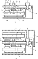
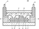
- FIG. 16 is a configuration diagram of a general conventional semiconductor module 500 described in Patent Document 1.
- the semiconductor module 500 includes an insulating substrate 54, a semiconductor chip 56, a base plate 57, a resin case 59, a metal wire 60, a gel 61, and a lid 62.
- the insulating substrate 54 includes a ceramic plate 51, a circuit plate 52 disposed on the front surface of the ceramic plate 51, and a metal plate 53 disposed on the back surface.
- a semiconductor chip 56 is joined to the circuit board 52 with solder 55.
- a metal base plate 57 is joined to the metal plate 53 via solder 55.
- the resin case 59 is bonded to the outer periphery of the base plate 57, and the external terminals 58 are insert-molded.
- the semiconductor chip 56 and the external terminal 58 are electrically connected by the metal wire 60.
- the resin case 59 is filled with a gel 61 which is an insulating sealing material.
- the resin lid 62 is fixed to the upper part of the resin case 59. Then, cooling fins (not shown) are attached to the base plate 57.
- This semiconductor module 500 is a single-sided cooling semiconductor device.
- the conventional semiconductor module 500 shown in FIG. 16 has the following problems. (1) Since the circuit board 52 is joined to one surface of the ceramic board 51, the area of the insulating substrate 54 is increased. (2) Since part of the wiring of the electric circuit is performed by the circuit board 52, when the configuration of the electric circuit is changed, the pattern of the circuit board 52 needs to be changed. It is necessary to change an assembly jig such as a mask. (3) Since part of the wiring of the electric circuit is performed by the metal wire 60, batch processing cannot be performed, the process time becomes long, and a large number of processing devices are required. (4) Since the wiring of the electric circuit is performed by the metal wire 60 and the external terminal 58, when different electric circuits are used, it is necessary to change the shape of the external terminal 58.
- the number of constituent members (metal wire 60, resin case 59, lid 62, gel 61, etc.) is large, and the manufacturing cost increases. (6) Since the electric circuit is composed of the metal wire 60, the circuit board 52, and the external terminal 58, and the distance between the circuit board facing the metal wire is large, the wiring inductance is increased.
- the object of the present invention is to solve the above-mentioned problems, reduce thermal resistance, reduce wiring inductance, secure ground insulation distance, simplify circuit configuration, reduce the number of steps required for connecting and joining components, and reducing
- An object of the present invention is to provide a semiconductor module that can be reduced in cost and size.
- a semiconductor module includes an insulating plate, a first wiring layer and a fourth wiring layer disposed on a main surface of the insulating plate, and opposite to the main surface.
- a second wiring layer and a third wiring layer disposed on the side surface; a first via disposed in the insulating plate and electrically and mechanically connected to the first wiring layer and the third wiring layer;
- a printed circuit board having a second via disposed in the insulating plate and electrically and mechanically connected to the second wiring layer and the fourth wiring layer, and disposed opposite to the first wiring layer.
- the second circuit board is disposed, and the second circuit board is disposed such that the third circuit board facing the third wiring layer is disposed.
- a semiconductor module capable of reducing thermal resistance, reducing wiring inductance, securing a ground insulation distance, simplifying a circuit configuration, reducing the number of steps required for connecting and joining components, reducing costs, and reducing the size of the semiconductor module. Can be provided.
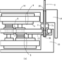
- FIG. 1 is a cross-sectional view of a semiconductor module 100 according to the first embodiment.
- FIG. 2 is an enlarged view of part A in FIG.
- FIG. 3 is a configuration diagram used to calculate the relationship between the thermal resistance Rth1 of the first semiconductor chip 6a and the filling rate of the first via 12a.
- FIG. 4 is a configuration diagram of the first via 12a.
- FIG. 5 is a diagram showing the relationship between the thermal resistance Rth1 and the filling rate of the first via 12a.
- FIG. 6 is a perspective plan view of each component of the diode module of the first embodiment.
- FIG. 7 is a perspective plan view of each component of the diode module of the first embodiment.
- FIG. 8 is a cross-sectional view showing a modification of the first embodiment.
- FIG. 1 is a cross-sectional view of a semiconductor module 100 according to the first embodiment.
- FIG. 2 is an enlarged view of part A in FIG.
- FIG. 3 is a configuration diagram used to calculate
- FIG. 9 is a manufacturing process sectional view of the semiconductor module 100 of the second embodiment.
- FIG. 10 is a manufacturing process sectional view of the semiconductor module 100 of the second embodiment following FIG.
- FIG. 11 is a manufacturing process sectional view of the semiconductor module 100 of the second embodiment following FIG.
- FIG. 12 is a manufacturing process sectional view of the semiconductor module 100 of the second embodiment following FIG.
- FIG. 13 is a manufacturing process sectional view of the semiconductor module 100 of the second embodiment following FIG.
- FIG. 14 is a manufacturing process sectional view of the semiconductor module of the second embodiment following FIG.
- FIG. 15 is a process diagram illustrating a process of forming a via.
- FIG. 16 is a configuration diagram of a conventional semiconductor module 500.
- FIG. 1 is a cross-sectional view of a semiconductor module 100 according to a first embodiment of the present invention.
- FIG. 2 is an enlarged view of part A in FIG.
- the semiconductor module 100 includes a printed circuit board 8, a first insulating substrate 4, a second insulating substrate 5, a first semiconductor chip 6a, a second semiconductor chip 6b, a first heat radiating member 16a, and a second heat radiating member. 16b.
- the first semiconductor chip 6a and the second semiconductor chip 6b can be electrically connected to an external circuit by an external terminal 9.
- the first semiconductor chip 6a is an upper chip
- the second semiconductor chip 6b is a lower chip.
- the printed circuit board 8 includes an insulating plate 8a, a first wiring layer 13a, a second wiring layer 13b, a third wiring layer 13c, a fourth wiring layer 13d, a first via 12a, and a second via 12b. is doing.
- the first wiring layer 13a and the fourth wiring layer 13d are arranged on the main surface of the insulating plate 8a, and the second wiring layer 13b and the third wiring layer 13c are arranged on the surface opposite to the main surface of the insulating plate 8a.
- the first wiring layer 13a and the third wiring layer 13c are electrically and mechanically connected by the first via 12a disposed in the insulating plate 8a.
- the second wiring layer 13b and the fourth wiring layer 13d are electrically and mechanically connected by the second via 12b disposed in the insulating plate 8a.
- the first via 12a and the second via 12b are formed of a conductor in which a large number of minute through holes 20 are formed in the insulating plate 8a and a metal is embedded in the through holes 20 by Cu (copper) plating or the like.
- Examples of the insulating plate 8a include a glass epoxy plate.
- the first insulating substrate 4 is configured by laminating a first circuit board 1a, a first ceramic plate 3a, and a first metal plate 2a.
- the first insulating substrate 4 is disposed to face the main surface of the printed circuit board 8. Further, the first circuit board 1a is arranged to face the first wiring layer 13a and the fourth wiring layer 13d.
- the second insulating substrate 5 is configured by laminating the second circuit board 1b and the third circuit board 1c, the second ceramic plate 3b, and the second metal plate 2b.
- the second insulating substrate 5 is disposed to face the surface opposite to the main surface of the printed circuit board 8.
- the second circuit board 1b is disposed to face the second wiring layer 13b
- the third circuit board 1c is disposed to face the third wiring layer 13c.
- the first ceramic plate 3a and the second ceramic plate 3b are made of a high thermal conductive ceramic such as alumina, aluminum nitride, or silicon nitride.
- the 1st circuit board 1a, the 2nd circuit board 1b, the 3rd circuit board 1c, the 1st metal plate 2a, and the 2nd metal plate 2b are comprised with high heat conductive metals, such as copper and aluminum.
- the first semiconductor chip 6a and the second semiconductor chip 6b are composed of power semiconductor elements such as an IGBT (insulated gate bipolar transistor), a power MOSFET, and an FWD (freewheeling diode).
- the first semiconductor chip 6a and the second semiconductor chip 6b include electrodes such as an emitter electrode, a collector electrode, and a gate electrode (not shown) on both surfaces.
- the first semiconductor chip 6a is sandwiched between the first wiring layer 13a and the first circuit board 1a, and both surfaces are electrically and mechanically connected by a conductive bonding material 7 such as solder.
- a conductive bonding material 7 such as solder.
- the second semiconductor chip 6b is sandwiched between the second wiring layer 13b and the second circuit board 1b, and both surfaces are electrically and mechanically connected by a conductive bonding material 7 such as solder.
- a conductive bonding material 7 such as solder.
- Conductive plating (for example, metal plating of Ti, Ni, Au, etc.) is performed on the front and back surfaces of the first semiconductor chip 6a and the second semiconductor chip 6b in order to improve the wettability of the bonding material 7 such as good solder. Is given.
- a conductive adhesive such as Ag paste or Cu paste may be used.
- the first heat radiating member 16a and the second heat radiating member 16b are made of metal.
- the first heat radiating member 16a is sandwiched between the third wiring layer 13c and the third circuit board 1c, and both ends are electrically and mechanically connected.
- the second heat radiating member 16b is sandwiched between the fourth wiring layer 13d and the first circuit board 1a, and both ends thereof are electrically and mechanically connected.
- solder may be used for the first heat radiating member 16a and the second heat radiating member 16b. In this case, since it is not necessary to prepare a separate bonding material, the manufacturing cost can be reduced.
- a copper block etc. can also be used for the 1st heat radiating member 16a and the 2nd heat radiating member 16b. In this case, the heat dissipation characteristics can be improved.
- the semiconductor module 100 also includes an external terminal 9 that is bonded via the through via 11 of the printed circuit board 8 and is electrically connected to at least one of the first wiring layer 13a and the second wiring layer 13b. Moreover, the whole is sealed so that the external terminals 9 and the second metal plate 2b are exposed, and a sealing resin 10 that also functions as a housing is provided. Moreover, the conductor 17 which electrically connects the printed circuit board 8 and the 2nd circuit board 1b is provided.
- This semiconductor module 100 is used as a single-sided cooling semiconductor device by installing cooling fins (not shown) on the exposed lower surface of the second metal plate 2b.
- the printed circuit board 8, the first insulating substrate 4, the second insulating substrate 5, and the external terminals 9 constitute a predetermined electric circuit required for the semiconductor module 100.
- the first wiring layer 13a on which the first semiconductor chip 6a is disposed and the third wiring layer 13c facing each other with the insulating plate 8a interposed therebetween are connected by the first via 12a.
- the third wiring layer 13c and the third circuit board 1c are connected by the first heat radiating member 16a.
- the second wiring layer 13b in which the second semiconductor chip 6b is disposed and the fourth wiring layer 13d facing each other with the insulating plate 8a interposed therebetween are connected by the second via 12b.
- the fourth wiring layer 13d and the first circuit board 1a are connected by the second heat radiating member 16b.
- the creeping distance between the second metal plate 2b, which is the ground plane of the second insulating substrate 5, and the external terminal 9 can be increased. it can. Therefore, a sufficient ground insulation distance can be secured.
- the third wiring layer 13c and the third circuit board 1c are made of a metal that joins the first heat radiation member 16a to flow the heat of the first semiconductor chip 6a to the cooling fin through the second insulating substrate 5. It is a pad. Therefore, the third wiring layer 13c and the third circuit board 1c may not be used as electrical wiring. In this case, the second wiring layer 13b and the third wiring layer 13c may be configured integrally.
- FIG. 3 is a configuration diagram in the vicinity of the first semiconductor chip 6a used for calculating the relationship between the thermal resistance Rth1 of the first semiconductor chip 6a and the filling rate of the first via 12a.
- 3A is a cross-sectional view
- FIG. 3B is a plan view cut along line X1-X1 in FIG. 3A
- FIG. 3C is a plane cut along line X2-X2 in FIG. FIG.
- four vias are shown as shown in the plan view.
- the heat generated in the first semiconductor chip 6a is transmitted to the second insulating substrate 5 via the first via 12a of the printed circuit board 8, and is radiated to the cooling fin (not shown).
- the thermal resistance Rth1 is determined based on the heat conduction path from the first semiconductor chip 6a to the second metal plate 2b.
- the thermal resistance Rth1 greatly depends on the structure of the first via 12a.
- the thermal resistance Rth2 does not depend on the via structure.
- FIG. 4 is a configuration diagram of the first via 12a
- FIG. 4 (a) is a plan view
- FIG. 4 (b) is a cross-sectional view taken along line XX of FIG. 4 (a).
- the first via 12a has a structure in which metal is embedded in a large number of minute through holes 20 formed in the insulating plate 8a of the printed circuit board 8, and fine-line columnar conductors 21 are gathered.
- the planar shape of the through-hole 20 is shown as a circular shape, but is not limited thereto, and may be a polygonal shape or a slit shape.
- the upper and lower first wiring layers 13a and the third wiring layers 13c are indicated by dotted lines.
- FIG. 5 is a diagram showing the relationship between the thermal resistance Rth1 calculated using the configuration of FIG. 3 and the filling rate of the first via 12a.
- FIG. 5 (a) shows the thickness of the insulating plate 8a of the printed circuit board 8.
- 5 (b) shows a case where the thickness of the insulating plate 8a of the printed circuit board 8 is about three times that of FIG. 5 (a).
- the burying rate was expressed as a percentage (%) of the area of the buried first via 12a with respect to the area of the semiconductor chip.
- the size of the first semiconductor chip 6a and the second semiconductor chip 6b is about 5 mm ⁇ , and the chip area is about 25 mm 2 .
- the first via 12a and the second via 12b are filled with the Cu plating film as described above, and the first wiring layer 13a and the third wiring layer 13c are the Cu plating film.
- the thermal conductivity of the insulating plate 8a of the printed circuit board 8 is as extremely small as about 1/1000 of the thermal conductivity of Cu, so that the thermal resistance at locations other than the vias of the printed circuit board 8 increases.
- the thermal resistance Rth2 does not pass through the via, it is constant at about 0.5 ° C./W regardless of the filling rate.
- the thermal resistance Rth1 is not preferable in both cases of FIG. 5A and FIG. 5B, when the embedding rate is 10% or less, the rise of Rth1 becomes remarkable. For this reason, it is desirable to set the embedding rate to 10% or more.
- the filling rate of the second via 12b is also preferably 10% or more.
- the thermal resistance may be reduced as compared with the case of using a glass epoxy plate or the like.
- the via may be formed by a method other than plating (for example, sputtering).
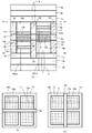
- FIG. 6 is a perspective plan view of each component viewed from the top in the vertical direction for each laminated component.
- 6A is a plan view of the first circuit board 1a of the first insulating substrate 4
- FIG. 6B is a plan view of the first wiring layer 13a and the fourth wiring layer 13d of the printed circuit board 8
- FIG. 6C is a plan view of the second wiring layer 13b and the third wiring layer 13c of the printed circuit board 8
- FIG. 6D is a plan view of the second circuit board 1b and the third circuit board 1c of the second insulating substrate 5.
- FIG. 6 (e) is a circuit diagram. This circuit diagram is a diode module in which a three-phase bridge (converter circuit) is formed by a diode. In this figure, the direction of current is reversed in part B, and the wiring inductance can be reduced.
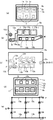
- FIG. 7 is a diagram when the wiring layers on both sides of the printed board 8 of FIG. 6 are changed. As shown in FIG. 7, different electrical circuits can be easily configured by changing the wiring layers on both sides of the printed circuit board 8. In FIG. 7, the direction of current is reversed at part B, and the wiring inductance can be reduced.
- the diode module can be easily changed to an IGBT module or the like.
- the constituent members (aluminum wire, resin case, gel, etc.) constituting the conventional semiconductor module 500 can be reduced, and the cost can be reduced.
- the semiconductor module can be downsized by dividing and arranging a plurality of semiconductor chips on both sides of the printed circuit board 8. Further, by reducing the current directions of the first circuit board 1a, the second circuit board 1b, the third circuit board 1c, and the respective wiring layers of the printed circuit board 8 facing them, the wiring inductance can be reduced. Can do. Furthermore, as shown in FIGS. 6 and 7, the wiring inductance can be reduced by making the current directions of the wiring layers on both sides of the printed circuit board 8 opposite to each other. This is a mutual induction effect that occurs between them.
- the first metal plate 2a of the first insulating substrate 4 serves as a shielding plate against radiated electromagnetic noise, and upwards from the first semiconductor chip 6a, the second semiconductor chip 6b, and the like. Radiated electromagnetic noise can be reduced. Further, by disposing the first via 12a and the first heat radiating member 16a, it is possible to effectively cool both surfaces of the heat generated from the first semiconductor chip 6a. Similarly, by disposing the second via 12b and the second heat radiating member 16b, it is possible to effectively cool both surfaces of the heat generated from the second semiconductor chip 6b.
- FIG. 8 is a cross-sectional view when the first heat dissipating member 16a is replaced with a high thermal conductive insulator 18 as a modification of the first embodiment.
- the cooling fin is provided on the upper first insulating substrate 4, but when the first metal plate 2a is sealed to be exposed, the cooling fin is provided. You can also. This further improves the efficiency of double-sided cooling from the semiconductor chip.
- the base surface of the external terminal 9 may be covered with an insulating layer or the external terminal 9 may be placed in an insulating tube.
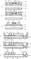
- 9 to 14 show a method for manufacturing the semiconductor module 100 of the second embodiment.
- the left column is a process related to the first insulating substrate 4, and the right column is a process related to the second insulating substrate 5.
- the metal mask 30 is mounted on each of the first insulating substrate 4 and the second insulating substrate 5 (FIG. 9A).
- the solder paste 7a which solidifies and becomes the joining material 7 is apply
- the solder paste 7a is placed on the first circuit board 1a and the second circuit board 1b (FIG. 9C).
- the first semiconductor chip 6a and the second semiconductor chip 6b are placed on the solder paste 7a, and the solder paste 7a is solidified by processing in a reflow furnace (not shown) (FIG. 9D).
- the metal mask 31 is placed on the second insulating substrate 5 (FIG. 10E).
- the opening 32 of the metal mask 31 is formed at a location where the second semiconductor chip 6 b is located and a location where the first heat radiating member 16 a and the solder paste 7 a serving as the conductor 17 are disposed.
- a solder paste 7a is applied on the metal mask 31 (FIG. 10F).
- the solder paste 7a is placed on the second circuit board 1b and the third circuit board 1c (FIG. 10 (g)).
- a metal mask 33 is placed on the main surface of the printed circuit board 8 (FIG. 10H).
- a through via 11 into which the external terminal 9 is inserted is formed at the end of the printed board 8, and a metal layer 37 is formed on the side wall of the through via 11.
- the first via 12a and the second via 12b are already formed in the printed circuit board 8.
- the solder paste 7a is applied on the metal mask 33 (FIG. 10 (i)).
- the solder paste 7 a is placed on the main surface of the printed circuit board 8.
- the solder paste may be applied using a dispenser or the like.
- the printed circuit board 8 is placed on the second insulating substrate 5 fixed to the fixing jig 15 (FIG. 11 (k)).
- the fixing jig 15 has a recess 38 into which the external terminal 9 is inserted.
- the first insulating substrate 4 is placed on the main surface of the printed circuit board 8 with the first circuit board 1a facing downward. Further, a fixing jig 14 for fixing the first insulating substrate 4 is placed thereon (FIG. 11 (l)).
- the fixing jig 14 and the fixing jig 15 are made of a material such as a carbon ceramic material that has a small coefficient of linear expansion and does not adhere to solder.
- the fixing jig 14 and the fixing jig 15 are processed so that the first insulating substrate 4, the second insulating substrate 5, the printed board 8, and the like can be positioned.
- the fixing jig 14 is provided with a through hole 39 for inserting the external terminal 9.
- the lower end of the external terminal 9 is fixed at a position higher than the second metal plate 2b.
- the columnar external terminals 9 are inserted into the through holes 39 (FIG. 12 (m)).
- the external terminal 9 is disposed through the through via 11 on which the solder paste 7a is placed.
- each member is soldered simultaneously.
- the fixing jig 14 and the fixing jig 15 are removed, and a structure 34 in which each member is soldered is completed (FIG. 13 (n)).
- the structure 34 is fixed to the casting jig 35b, and the casting jig 35a is further covered, and the thermosetting resin 40 is injected therein (FIG. 13 (o)).
- the casting jig 35a is provided with a through hole 35c through which the external terminal 9 passes.
- thermosetting resin 40 is cured to form the sealing resin 10. Further, the structure 34 covered with the sealing resin 10 is taken out from the casting jigs 35a and 35b, and the semiconductor module 100 is completed (FIG. 14 (p)).
- the main processes for assembling the semiconductor module 100 in the second embodiment are the following three processes.
- FIG. 15 is a process diagram illustrating a process of forming the first via 12a.
- many minute through holes 20 are formed in the insulating plate 8a of the printed circuit board 8 (FIG. 15A).
- the diameter of the through hole 20 is set to be within twice the thickness of the first wiring layer 13a.
- the Cu plating film 21a is formed on both surfaces of the insulating plate 8a by plating.
- the diameter of the through hole 20 is within twice the thickness of the Cu plating film 21a, that is, the thickness of the first wiring layer 13a, the Cu plating films 21a formed on the side walls of the through hole 20 Contact is made inside the through-hole 20 (FIG. 15B). By this contact, the inside of the through hole 20 is filled with the Cu plating film 21a, and the conductor 21 is formed. The aggregate of the conductors 21 is the first via 12a.
- the Cu plating films 21a on both surfaces of the insulating plate 8a are patterned by photolithography to form the first wiring layer 13a and the third wiring layer 13c (FIG. 15C).
- the first via 12a electrically and mechanically connected to the first wiring layer 13a and the third wiring layer 13c is formed.
- the first via 12a is formed by a plating method is shown, but it can also be formed by using a sputtering method, a vapor deposition method, or the like.
Landscapes
- Cooling Or The Like Of Semiconductors Or Solid State Devices (AREA)
- Physics & Mathematics (AREA)
- Geometry (AREA)
- Chemical & Material Sciences (AREA)
- Engineering & Computer Science (AREA)
- Ceramic Engineering (AREA)
Abstract
Description
(1)回路板52をセラミック板51の一つの面に接合するため、絶縁基板54の面積が大きくなる。
(2)電気回路の配線の一部を回路板52で行なっているため、電気回路の構成を変更する場合には回路板52のパターンを変更する必要があり、その都度、絶縁基板54と金属マスクなどの組立治具を変更する必要がある。
(3)電気回路の配線の一部を金属ワイヤ60で行なっているため、バッチ処理ができずに工程時間が長くなり、処理装置が多数必要になる。
(4)電気回路の配線を金属ワイヤ60と外部端子58で行なっているため、異なる電気回路にする場合、外部端子58の形状を変更する必要があり、外部端子58の加工に伴って金型がその都度必要になる。
(5)構成部材数(金属ワイヤ60、樹脂ケース59、蓋62およびゲル61など)が多く、製造コストが高くなる。
(6)電気回路が金属ワイヤ60と回路板52および外部端子58で構成され、金属ワイヤと対向する回路板の距離が大きいため、配線インダクタンスが大きくなる。
第1セラミック板3aおよび第2セラミック板3bは、アルミナや窒化アルミ、窒化珪素などの高熱伝導セラミックなどで構成される。また、第1回路板1a、第2回路板1b、第3回路板1c、第1金属板2a、第2金属板2bは、銅やアルミなどの高熱伝導金属で構成される。
第1半導体チップ6aは、第1配線層13aおよび第1回路板1aとの間に挟まれ、両面がはんだなどの導電性の接合材7で電気的かつ機械的に接続されている。これにより、第1配線層13aおよび第1回路板1aと、第1半導体チップ6aの両面の電極がそれぞれ電気的に接続される。
この第1半導体チップ6a及び第2半導体チップ6bのそれぞれの表裏面には良好なはんだなどの接合材7の濡れ性を高めるために導電性めっき(例えば、Ti,Ni,Auなどの金属めっき)が施されている。接合材7としては、AgペーストやCuペーストなどの導電性接着剤を用いても構わない。
第1ビア12aは、プリント基板8の絶縁板8aに形成された多数の微小な貫通孔20に金属を埋め込み、細線の柱状の導体21が集合した構造をしている。ここでは、貫通孔20の平面形状は円形の場合を示したが、これに限るものではなく、多角形やスリット状の場合もある。図4では、上下の第1配線層13a及び第3配線層13cを点線で示した。
一方、熱抵抗Rth1は、図5(a)及び図5(b)のいずれの場合も、埋め込み率が10%以下ではRth1の上昇が顕著となり好ましくない。このため、埋め込み率を10%以上にするのが望ましい。
上記結果については、第2半導体チップ6bから第2ビア12bを経由した、第1絶縁基板4への熱伝導についても同様である。そのため、第2ビア12bの埋め込み率についても、10%以上が望ましい。
尚、プリント基板8の絶縁板8aとしてセラミック板を用いると、例えば、ガラスエポキシ板などを用いる場合より熱抵抗を低減できるのでよい。その場合には、ビアはめっき以外の方法(例えばスパッタ法など)で形成すればよい。
図7に示すように、プリント基板8の両面の配線層を変更することで、異なる電気回路を容易に構成することができる。なお、図7ではB部で電流の向きが逆になり配線インダクタンスを小さくできる。
また、上記のダイオードモジュールは、容易にIGBTモジュールなどに変更することが可能である。
また、第1回路板1aや第2回路板1b、第3回路板1cと、これらに対向するプリント基板8の各配線層の電流方向を互いに逆方向にすることにより、配線インダクタンスを低減することができる。さらに、図6や図7で示した通り、プリント基板8の両面の配線層の電流方向を互いに逆方向にすることにより、配線インダクタンスを低減することができる。これは、これらの間で生じる相互誘導の効果である。
また、第1ビア12aと第1放熱部材16aを配置することで、第1半導体チップ6aから発生した熱を効果的に両面冷却することが可能となる。同様に、第2ビア12bと第2放熱部材16bを配置することで、第2半導体チップ6bから発生した熱を効果的に両面冷却することが可能となる。
まず、第1絶縁基板4及び第2絶縁基板5のそれぞれに、金属マスク30を載置する(図9(a))。
次に、金属マスク30上に、固化して接合材7になるはんだペースト7aを塗布する(図9(b))。
次に、金属マスク30を取り外すと、第1回路板1a及び第2回路板1b上にはんだペースト7aが載置される(図9(c))。
次に、上記のはんだペースト7a上に第1半導体チップ6a及び第2半導体チップ6bを載置し、図示しないリフロー炉で処理してはんだペースト7aを固化する(図9(d))。
次に、金属マスク31上にはんだペースト7aを塗布する(図10(f))。
次に、金属マスク31を取り外すと、第2回路板1b及び第3回路板1c上にはんだペースト7aが載置される(図10(g))。
次に、金属マスク33上にはんだペースト7aを塗布する(図10(i))。
次に、金属マスク33を取り外すと、プリント基板8の主面上にはんだペースト7aが載置される。
尚、上記のはんだ印刷工程は、ディスペンサーなどによりはんだペーストを塗布してもよい。
次に、プリント基板8の主面上に、第1絶縁基板4を第1回路板1aを下向きにして載置する。さらに、その上に第1絶縁基板4を固定する固定治具14を載置する(図11(l))。なお、固定治具14および固定治具15は、カーボン・セラミック材など線膨張係数が小さく、はんだが付着しない材料で構成されている。また、固定治具14および固定治具15には、第1絶縁基板4や第2絶縁基板5、プリント基板8などの位置決めができるように加工が施されている。また、固定治具14には、外部端子9を挿入するために貫通孔39が設けられている。また、対地絶縁距離を確保するために、外部端子9の下端は第2金属板2bよりも高い位置に固定する。
次に、構造体34を注型治具35bに固定し、さらに注型治具35aを被せ、その内部に熱硬化性樹脂40を注入する(図13(o))。なお、注型治具35aには、外部端子9を貫通させる貫通孔35cが設けられている。
(1)第1絶縁基板4及び第2絶縁基板5に第1半導体チップ6a及び第2半導体チップ6bを固着する工程。
(2)プリント基板8と、その両面に配置される第1絶縁基板4及び第2絶縁基板5と、外部端子9をはんだペースト7aを用いて同時に固着する工程。
(3)封止樹脂10で被覆する工程。
そのため、バッチ処理による組立工程時間の削減が可能となり、製造コストを低減できる。
図15は、第1ビア12aを形成する工程を説明した工程図である。
まず、プリント基板8の絶縁板8aに微小な貫通孔20を多数形成する(図15(a))。貫通孔20の直径は、第1配線層13aの厚さの2倍以内とする。
次に、めっき処理でCuめっき膜21aを絶縁板8aの両面に形成する。このとき、貫通孔20の直径をCuめっき膜21aの厚さ、すなわち第1配線層13aの厚さの2倍以内にすることで、貫通孔20の側壁に形成されたCuめっき膜21a同士が貫通孔20の内部で接触する(図15(b))。この接触によって貫通孔20内はCuめっき膜21aで充填されて導体21が形成される。この導体21の集合体が第1ビア12aである。
これらの工程により、第1配線層13aおよび第3配線層13cに電気的かつ機械的に接続された第1ビア12aが形成される。
ここでは、第1ビア12aはめっき法で形成した場合を示したが、スパッタ法や蒸着法などを用いても形成することもできる。
1b 第2回路板
1c 第3回路板
2a 第1金属板
2b 第2金属板
3a 第1セラミック板
3b 第2セラミック板
4 第1絶縁基板
5 第2絶縁基板
6a 第1半導体チップ
6b 第2半導体チップ
7 接合材
7a はんだペースト
8 プリント基板
8a 絶縁板
9 外部端子
10 封止樹脂
11 貫通ビア
12a 第1ビア
12b 第2ビア
13 配線層
13a 第1配線層
13b 第2配線層
13c 第3配線層
13d 第4配線層
14,15 固定治具
16a 第1放熱部材
16b 第2放熱部材
17 導電体
18 高熱伝導絶縁体
20 貫通孔
21 導体
21a Cuめっき膜
30,31,33 金属マスク
32 開口部
34 構造体
35a,35b 注型治具
37 金属層
38 凹部
39 貫通孔
40 熱硬化性樹脂
100 半導体モジュール
Claims (10)
- 絶縁板と、前記絶縁板の主面に配置された第1配線層および第4配線層と、前記主面の反対側の面に配置された第2配線層および第3配線層と、前記絶縁板内に配置され前記第1配線層及び前記第3配線層に電気的かつ機械的に接続された第1ビアと、前記絶縁板内に配置され前記第2配線層及び前記第4配線層に電気的かつ機械的に接続された第2ビアとを有するプリント基板と、
前記第1配線層に対向して配置され、前記第1配線層および前記第4配線層との対向面に第1回路板が配置される第1絶縁基板と、
前記第2配線層に対向して配置され、前記第2配線層と対向した第2回路板が配置され、前記第3配線層と対向した第3回路板が配置される第2絶縁基板と、
前記第1配線層と前記第1回路板との間に挟まれ、両面がそれぞれ導電性の接合材で固定される第1半導体チップと、
前記第2配線層と前記第2回路板との間に挟まれ、両面がそれぞれ導電性の接合材で固定される第2半導体チップと、
前記第3配線層と前記第3回路板との間に挟まれて固定された第1放熱部材と、
前記第4配線層と前記第1回路板との間に挟まれて固定された第2放熱部材と、
を備えた半導体モジュール。 - 前記絶縁板上における前記第1ビアの面積が、前記第1半導体チップの面積に対して10%以上である請求項1に記載の半導体モジュール。
- 前記絶縁板上における前記第2ビアの面積が、前記第2半導体チップの面積に対して10%以上である請求項1に記載の半導体モジュール。
- 前記第1放熱部材および前記第2放熱部材は、導電性接合材もしくは金属板で構成されている請求項1に記載の半導体モジュール。
- 前記第2回路板および前記第3回路板が一体で構成され、前記第1放熱部材が高熱伝導絶縁体で構成されている請求項1に記載の半導体モジュール。
- 前記第2絶縁基板の第2回路板が配置される面の反対面に、金属板が配置されている請求項1に記載の半導体モジュール。
- 前記第1絶縁基板の第1回路板が配置される面の反対面に、金属板が配置されている請求項1に記載の半導体モジュール。
- 前記第1ビア及び第2ビアが、前記プリント基板の絶縁板に配置された複数の貫通孔内を埋めた柱状の導体からなる請求項1に記載の半導体モジュール。
- 前記接合材および前記放熱部材が、いずれもはんだである請求項1に記載の半導体モジュール。
- 前記第1配線層もしくは第2配線層と電気的に接続されている外部端子をさらに備えた請求項1に記載の半導体モジュール。
Priority Applications (3)
| Application Number | Priority Date | Filing Date | Title |
|---|---|---|---|
| JP2015540430A JP5975180B2 (ja) | 2013-10-03 | 2014-08-29 | 半導体モジュール |
| DE112014001487.7T DE112014001487B4 (de) | 2013-10-03 | 2014-08-29 | Halbleitermodul |
| US14/877,389 US9530707B2 (en) | 2013-10-03 | 2015-10-07 | Semiconductor module |
Applications Claiming Priority (2)
| Application Number | Priority Date | Filing Date | Title |
|---|---|---|---|
| JP2013207878 | 2013-10-03 | ||
| JP2013-207878 | 2013-10-03 |
Related Child Applications (1)
| Application Number | Title | Priority Date | Filing Date |
|---|---|---|---|
| US14/877,389 Continuation US9530707B2 (en) | 2013-10-03 | 2015-10-07 | Semiconductor module |
Publications (1)
| Publication Number | Publication Date |
|---|---|
| WO2015049944A1 true WO2015049944A1 (ja) | 2015-04-09 |
Family
ID=52778539
Family Applications (1)
| Application Number | Title | Priority Date | Filing Date |
|---|---|---|---|
| PCT/JP2014/072827 Ceased WO2015049944A1 (ja) | 2013-10-03 | 2014-08-29 | 半導体モジュール |
Country Status (4)
| Country | Link |
|---|---|
| US (1) | US9530707B2 (ja) |
| JP (1) | JP5975180B2 (ja) |
| DE (1) | DE112014001487B4 (ja) |
| WO (1) | WO2015049944A1 (ja) |
Cited By (5)
| Publication number | Priority date | Publication date | Assignee | Title |
|---|---|---|---|---|
| WO2018138902A1 (ja) * | 2017-01-30 | 2018-08-02 | 三菱電機株式会社 | パワー半導体装置の製造方法およびパワー半導体装置 |
| US20220077103A1 (en) * | 2020-09-10 | 2022-03-10 | Fuji Electric Co., Ltd. | Semiconductor device and manufacturing method of semiconductor device |
| WO2022118510A1 (ja) * | 2020-12-03 | 2022-06-09 | 株式会社日立製作所 | 絶縁基板および電力変換装置 |
| JP2023071301A (ja) * | 2021-11-11 | 2023-05-23 | 新光電気工業株式会社 | 半導体装置 |
| DE112021007799T5 (de) | 2021-06-09 | 2024-04-11 | Mitsubishi Electric Corporation | Halbleitermodul und leistungswandler |
Families Citing this family (25)
| Publication number | Priority date | Publication date | Assignee | Title |
|---|---|---|---|---|
| DE112013007709T5 (de) * | 2013-12-24 | 2016-09-15 | Mitsubishi Electric Corporation | Elektrischer Leistungswandler und Leistungsmodul |
| US9892993B2 (en) * | 2015-04-28 | 2018-02-13 | Shindengen Electric Manufacturing Co., Ltd. | Semiconductor module having stacked insulated substrate structures |
| JP6813259B2 (ja) * | 2015-06-29 | 2021-01-13 | 富士電機株式会社 | 半導体装置 |
| EP3413349A4 (en) * | 2016-02-03 | 2019-09-11 | Shindengen Electric Manufacturing Co. Ltd. | SEMICONDUCTOR COMPONENT AND METHOD FOR PRODUCING SEMICONDUCTOR COMPONENT |
| TWI697058B (zh) | 2016-03-30 | 2020-06-21 | 胡志良 | 具堅實導電及導熱性銅質線路之電路元件封裝方法及其封裝體 |
| DE202016004404U1 (de) * | 2016-07-12 | 2016-08-03 | Würth Elektronik eiSos Gmbh & Co. KG | Hochintegrierter Spannungsumsetzer |
| DE102016117841A1 (de) | 2016-09-21 | 2018-03-22 | HYUNDAI Motor Company 231 | Packung mit aufgerauter verkapselter Oberfläche zur Förderung einer Haftung |
| US10163751B2 (en) | 2016-11-29 | 2018-12-25 | Taiwan Semiconductor Manufacturing Company, Ltd. | Heat transfer structures and methods for IC packages |
| FR3073978B1 (fr) * | 2017-11-17 | 2022-10-28 | Inst Vedecom | Module electronique de puissance et systeme electronique comprenant un tel module electronique |
| CN110164858B (zh) | 2018-02-16 | 2023-05-05 | 株式会社电装 | 半导体器件 |
| KR102048478B1 (ko) * | 2018-03-20 | 2019-11-25 | 엘지전자 주식회사 | 양면냉각형 파워 모듈 및 그의 제조 방법 |
| EP3557614A1 (de) * | 2018-04-17 | 2019-10-23 | Siemens Aktiengesellschaft | Leistungsmodul mit einem leistungselektronischen bauelement auf einer substratplatte und leistungselektronische schaltung mit einem solchen leistungsmodul |
| JP7322369B2 (ja) * | 2018-09-21 | 2023-08-08 | 富士電機株式会社 | 半導体装置の製造方法 |
| JP2020126921A (ja) * | 2019-02-04 | 2020-08-20 | 株式会社村田製作所 | 高周波モジュールおよび通信装置 |
| JP7103256B2 (ja) * | 2019-02-13 | 2022-07-20 | 株式会社デンソー | 半導体装置 |
| JP7240221B2 (ja) * | 2019-03-28 | 2023-03-15 | 日立Astemo株式会社 | パワー半導体装置 |
| JP7156155B2 (ja) * | 2019-04-19 | 2022-10-19 | 三菱電機株式会社 | 半導体モジュール |
| JP6741135B1 (ja) * | 2019-10-02 | 2020-08-19 | 富士電機株式会社 | 半導体モジュール及び半導体モジュールの製造方法 |
| EP4178323B1 (en) * | 2020-07-06 | 2024-12-11 | Amosense Co.,Ltd | Power module |
| US12362332B2 (en) * | 2020-07-29 | 2025-07-15 | Mitsubishi Electric Corporation | Semiconductor device |
| DE102020130617B4 (de) * | 2020-11-19 | 2025-03-06 | Infineon Technologies Ag | Halbleiterpackages mit elektrischen Umverteilungsschichten unterschiedlicher Dicken und Verfahren zu deren Herstellung |
| JP7072698B1 (ja) * | 2021-03-26 | 2022-05-20 | 三菱電機株式会社 | 降圧コンバータ |
| TWI778816B (zh) * | 2021-09-28 | 2022-09-21 | 欣興電子股份有限公司 | 晶片互聯的封裝結構及其封裝方法 |
| CN114899156A (zh) * | 2022-03-31 | 2022-08-12 | 深圳基本半导体有限公司 | 金属垫片和应用该金属垫片的双面散热功率模块 |
| EP4290574A1 (en) * | 2022-06-09 | 2023-12-13 | Mitsubishi Electric R&D Centre Europe B.V. | Power module with integrated power boards and pcb busbar |
Citations (5)
| Publication number | Priority date | Publication date | Assignee | Title |
|---|---|---|---|---|
| JPH0955459A (ja) * | 1995-06-06 | 1997-02-25 | Seiko Epson Corp | 半導体装置 |
| JP2000101018A (ja) * | 1998-09-25 | 2000-04-07 | Shindengen Electric Mfg Co Ltd | 電気装置 |
| JP2006134990A (ja) * | 2004-11-04 | 2006-05-25 | Fuji Electric Holdings Co Ltd | 半導体装置 |
| JP2008010768A (ja) * | 2006-06-30 | 2008-01-17 | Toshiba Corp | 電子機器および実装構造体 |
| JP2009117428A (ja) * | 2007-11-01 | 2009-05-28 | Hitachi Ltd | パワー半導体モジュールの製造方法、パワー半導体モジュールの製造装置、パワー半導体モジュール、及び接合方法 |
Family Cites Families (13)
| Publication number | Priority date | Publication date | Assignee | Title |
|---|---|---|---|---|
| JPS63283147A (ja) | 1987-05-15 | 1988-11-21 | Seiko Keiyo Kogyo Kk | 半導体装置 |
| JP3006585B2 (ja) | 1998-06-01 | 2000-02-07 | 富士電機株式会社 | 半導体装置 |
| JP3847676B2 (ja) | 2002-07-15 | 2006-11-22 | 三菱電機株式会社 | パワー半導体装置 |
| JP4438489B2 (ja) | 2004-04-13 | 2010-03-24 | 富士電機システムズ株式会社 | 半導体装置 |
| US7030317B1 (en) * | 2005-04-13 | 2006-04-18 | Delphi Technologies, Inc. | Electronic assembly with stacked integrated circuit die |
| JP2007012685A (ja) | 2005-06-28 | 2007-01-18 | Toyota Motor Corp | 半導体素子の冷却構造および半導体素子のモジュール構造 |
| US20080258293A1 (en) | 2007-04-17 | 2008-10-23 | Advanced Chip Engineering Technology Inc. | Semiconductor device package to improve functions of heat sink and ground shield |
| JP5067267B2 (ja) | 2008-06-05 | 2012-11-07 | 三菱電機株式会社 | 樹脂封止型半導体装置とその製造方法 |
| JP4907693B2 (ja) | 2009-05-13 | 2012-04-04 | 三菱電機株式会社 | 半導体装置 |
| JP2011086821A (ja) | 2009-10-16 | 2011-04-28 | Fuji Electric Systems Co Ltd | 半導体装置およびその製造方法 |
| JP5919692B2 (ja) | 2011-09-08 | 2016-05-18 | 富士電機株式会社 | 半導体装置および半導体装置の製造方法 |
| US8975711B2 (en) * | 2011-12-08 | 2015-03-10 | Infineon Technologies Ag | Device including two power semiconductor chips and manufacturing thereof |
| US8884343B2 (en) * | 2012-02-24 | 2014-11-11 | Texas Instruments Incorporated | System in package and method for manufacturing the same |
-
2014
- 2014-08-29 DE DE112014001487.7T patent/DE112014001487B4/de not_active Expired - Fee Related
- 2014-08-29 JP JP2015540430A patent/JP5975180B2/ja not_active Expired - Fee Related
- 2014-08-29 WO PCT/JP2014/072827 patent/WO2015049944A1/ja not_active Ceased
-
2015
- 2015-10-07 US US14/877,389 patent/US9530707B2/en not_active Expired - Fee Related
Patent Citations (5)
| Publication number | Priority date | Publication date | Assignee | Title |
|---|---|---|---|---|
| JPH0955459A (ja) * | 1995-06-06 | 1997-02-25 | Seiko Epson Corp | 半導体装置 |
| JP2000101018A (ja) * | 1998-09-25 | 2000-04-07 | Shindengen Electric Mfg Co Ltd | 電気装置 |
| JP2006134990A (ja) * | 2004-11-04 | 2006-05-25 | Fuji Electric Holdings Co Ltd | 半導体装置 |
| JP2008010768A (ja) * | 2006-06-30 | 2008-01-17 | Toshiba Corp | 電子機器および実装構造体 |
| JP2009117428A (ja) * | 2007-11-01 | 2009-05-28 | Hitachi Ltd | パワー半導体モジュールの製造方法、パワー半導体モジュールの製造装置、パワー半導体モジュール、及び接合方法 |
Cited By (11)
| Publication number | Priority date | Publication date | Assignee | Title |
|---|---|---|---|---|
| WO2018138902A1 (ja) * | 2017-01-30 | 2018-08-02 | 三菱電機株式会社 | パワー半導体装置の製造方法およびパワー半導体装置 |
| JPWO2018138902A1 (ja) * | 2017-01-30 | 2019-11-07 | 三菱電機株式会社 | パワー半導体装置の製造方法およびパワー半導体装置 |
| US11270982B2 (en) | 2017-01-30 | 2022-03-08 | Mitsubishi Electric Corporation | Method of manufacturing power semiconductor device and power semiconductor device |
| US20220077103A1 (en) * | 2020-09-10 | 2022-03-10 | Fuji Electric Co., Ltd. | Semiconductor device and manufacturing method of semiconductor device |
| US12230600B2 (en) * | 2020-09-10 | 2025-02-18 | Fuji Electric Co., Ltd. | Semiconductor device having through parts of different shapes |
| WO2022118510A1 (ja) * | 2020-12-03 | 2022-06-09 | 株式会社日立製作所 | 絶縁基板および電力変換装置 |
| JP2022088783A (ja) * | 2020-12-03 | 2022-06-15 | 株式会社日立製作所 | 絶縁基板および電力変換装置 |
| JP7535444B2 (ja) | 2020-12-03 | 2024-08-16 | 株式会社日立製作所 | 絶縁基板および電力変換装置 |
| DE112021007799T5 (de) | 2021-06-09 | 2024-04-11 | Mitsubishi Electric Corporation | Halbleitermodul und leistungswandler |
| JP2023071301A (ja) * | 2021-11-11 | 2023-05-23 | 新光電気工業株式会社 | 半導体装置 |
| JP7666781B2 (ja) | 2021-11-11 | 2025-04-22 | 新光電気工業株式会社 | 半導体装置 |
Also Published As
| Publication number | Publication date |
|---|---|
| JP5975180B2 (ja) | 2016-08-23 |
| JPWO2015049944A1 (ja) | 2017-03-09 |
| DE112014001487T5 (de) | 2015-12-10 |
| DE112014001487B4 (de) | 2021-03-04 |
| US9530707B2 (en) | 2016-12-27 |
| US20160027711A1 (en) | 2016-01-28 |
Similar Documents
| Publication | Publication Date | Title |
|---|---|---|
| JP5975180B2 (ja) | 半導体モジュール | |
| JP4438489B2 (ja) | 半導体装置 | |
| TWI567896B (zh) | 三維空間封裝結構及其製造方法 | |
| JP5788585B2 (ja) | 電子モジュールおよびその製造方法 | |
| JP2014199829A (ja) | 半導体モジュール及びそれを搭載したインバータ | |
| WO2019064775A1 (ja) | 半導体装置およびその製造方法 | |
| CN103972277B (zh) | 半导体装置及其制造方法 | |
| JP2019071412A (ja) | チップパッケージ | |
| CN112713120A (zh) | 功率电子组件及其产生方法 | |
| JP4967701B2 (ja) | 電力半導体装置 | |
| US20210184023A1 (en) | Semiconductor device | |
| JP2017143227A (ja) | 半導体集積回路素子の放熱構造、ならびに、半導体集積回路素子及びその製造方法 | |
| JP3935381B2 (ja) | 両面電極半導体素子を有する電子回路装置及び該電子回路装置の製造方法 | |
| JP2017123360A (ja) | 半導体モジュール | |
| US20180040562A1 (en) | Elektronisches modul und verfahren zu seiner herstellung | |
| JP5477157B2 (ja) | 半導体装置 | |
| JP5682511B2 (ja) | 半導体モジュール | |
| JP5619232B2 (ja) | 半導体装置および電極用部材の製造方法 | |
| CN110602923A (zh) | 封装模块及其封装方法、电子设备 | |
| US11217512B2 (en) | Semiconductor module | |
| JP4810898B2 (ja) | 半導体装置 | |
| JP2017139303A (ja) | 回路構成体およびその製造方法 | |
| CN104867903A (zh) | 电子模块 | |
| JP2016096190A (ja) | 電子装置 | |
| TWI831247B (zh) | 功率模組及其製作方法 |
Legal Events
| Date | Code | Title | Description |
|---|---|---|---|
| 121 | Ep: the epo has been informed by wipo that ep was designated in this application |
Ref document number: 14851147 Country of ref document: EP Kind code of ref document: A1 |
|
| ENP | Entry into the national phase |
Ref document number: 2015540430 Country of ref document: JP Kind code of ref document: A |
|
| WWE | Wipo information: entry into national phase |
Ref document number: 1120140014877 Country of ref document: DE Ref document number: 112014001487 Country of ref document: DE |
|
| 122 | Ep: pct application non-entry in european phase |
Ref document number: 14851147 Country of ref document: EP Kind code of ref document: A1 |