WO2015012228A1 - タッチパネル用ネガ型感光性白色組成物、タッチパネル及びタッチパネルの製造方法 - Google Patents
タッチパネル用ネガ型感光性白色組成物、タッチパネル及びタッチパネルの製造方法 Download PDFInfo
- Publication number
- WO2015012228A1 WO2015012228A1 PCT/JP2014/069221 JP2014069221W WO2015012228A1 WO 2015012228 A1 WO2015012228 A1 WO 2015012228A1 JP 2014069221 W JP2014069221 W JP 2014069221W WO 2015012228 A1 WO2015012228 A1 WO 2015012228A1
- Authority
- WO
- WIPO (PCT)
- Prior art keywords
- touch panel
- negative photosensitive
- white
- composition
- cured film
- Prior art date
- Legal status (The legal status is an assumption and is not a legal conclusion. Google has not performed a legal analysis and makes no representation as to the accuracy of the status listed.)
- Ceased
Links
Images






Classifications
-
- G—PHYSICS
- G03—PHOTOGRAPHY; CINEMATOGRAPHY; ANALOGOUS TECHNIQUES USING WAVES OTHER THAN OPTICAL WAVES; ELECTROGRAPHY; HOLOGRAPHY
- G03F—PHOTOMECHANICAL PRODUCTION OF TEXTURED OR PATTERNED SURFACES, e.g. FOR PRINTING, FOR PROCESSING OF SEMICONDUCTOR DEVICES; MATERIALS THEREFOR; ORIGINALS THEREFOR; APPARATUS SPECIALLY ADAPTED THEREFOR
- G03F7/00—Photomechanical, e.g. photolithographic, production of textured or patterned surfaces, e.g. printing surfaces; Materials therefor, e.g. comprising photoresists; Apparatus specially adapted therefor
- G03F7/004—Photosensitive materials
- G03F7/075—Silicon-containing compounds
- G03F7/0757—Macromolecular compounds containing Si-O, Si-C or Si-N bonds
-
- G—PHYSICS
- G03—PHOTOGRAPHY; CINEMATOGRAPHY; ANALOGOUS TECHNIQUES USING WAVES OTHER THAN OPTICAL WAVES; ELECTROGRAPHY; HOLOGRAPHY
- G03F—PHOTOMECHANICAL PRODUCTION OF TEXTURED OR PATTERNED SURFACES, e.g. FOR PRINTING, FOR PROCESSING OF SEMICONDUCTOR DEVICES; MATERIALS THEREFOR; ORIGINALS THEREFOR; APPARATUS SPECIALLY ADAPTED THEREFOR
- G03F7/00—Photomechanical, e.g. photolithographic, production of textured or patterned surfaces, e.g. printing surfaces; Materials therefor, e.g. comprising photoresists; Apparatus specially adapted therefor
- G03F7/0005—Production of optical devices or components in so far as characterised by the lithographic processes or materials used therefor
- G03F7/0007—Filters, e.g. additive colour filters; Components for display devices
-
- G—PHYSICS
- G03—PHOTOGRAPHY; CINEMATOGRAPHY; ANALOGOUS TECHNIQUES USING WAVES OTHER THAN OPTICAL WAVES; ELECTROGRAPHY; HOLOGRAPHY
- G03F—PHOTOMECHANICAL PRODUCTION OF TEXTURED OR PATTERNED SURFACES, e.g. FOR PRINTING, FOR PROCESSING OF SEMICONDUCTOR DEVICES; MATERIALS THEREFOR; ORIGINALS THEREFOR; APPARATUS SPECIALLY ADAPTED THEREFOR
- G03F7/00—Photomechanical, e.g. photolithographic, production of textured or patterned surfaces, e.g. printing surfaces; Materials therefor, e.g. comprising photoresists; Apparatus specially adapted therefor
- G03F7/0035—Multiple processes, e.g. applying a further resist layer on an already in a previously step, processed pattern or textured surface
-
- G—PHYSICS
- G03—PHOTOGRAPHY; CINEMATOGRAPHY; ANALOGOUS TECHNIQUES USING WAVES OTHER THAN OPTICAL WAVES; ELECTROGRAPHY; HOLOGRAPHY
- G03F—PHOTOMECHANICAL PRODUCTION OF TEXTURED OR PATTERNED SURFACES, e.g. FOR PRINTING, FOR PROCESSING OF SEMICONDUCTOR DEVICES; MATERIALS THEREFOR; ORIGINALS THEREFOR; APPARATUS SPECIALLY ADAPTED THEREFOR
- G03F7/00—Photomechanical, e.g. photolithographic, production of textured or patterned surfaces, e.g. printing surfaces; Materials therefor, e.g. comprising photoresists; Apparatus specially adapted therefor
- G03F7/004—Photosensitive materials
- G03F7/027—Non-macromolecular photopolymerisable compounds having carbon-to-carbon double bonds, e.g. ethylenic compounds
-
- G—PHYSICS
- G03—PHOTOGRAPHY; CINEMATOGRAPHY; ANALOGOUS TECHNIQUES USING WAVES OTHER THAN OPTICAL WAVES; ELECTROGRAPHY; HOLOGRAPHY
- G03F—PHOTOMECHANICAL PRODUCTION OF TEXTURED OR PATTERNED SURFACES, e.g. FOR PRINTING, FOR PROCESSING OF SEMICONDUCTOR DEVICES; MATERIALS THEREFOR; ORIGINALS THEREFOR; APPARATUS SPECIALLY ADAPTED THEREFOR
- G03F7/00—Photomechanical, e.g. photolithographic, production of textured or patterned surfaces, e.g. printing surfaces; Materials therefor, e.g. comprising photoresists; Apparatus specially adapted therefor
- G03F7/004—Photosensitive materials
- G03F7/027—Non-macromolecular photopolymerisable compounds having carbon-to-carbon double bonds, e.g. ethylenic compounds
- G03F7/028—Non-macromolecular photopolymerisable compounds having carbon-to-carbon double bonds, e.g. ethylenic compounds with photosensitivity-increasing substances, e.g. photoinitiators
- G03F7/029—Inorganic compounds; Onium compounds; Organic compounds having hetero atoms other than oxygen, nitrogen or sulfur
-
- G—PHYSICS
- G03—PHOTOGRAPHY; CINEMATOGRAPHY; ANALOGOUS TECHNIQUES USING WAVES OTHER THAN OPTICAL WAVES; ELECTROGRAPHY; HOLOGRAPHY
- G03F—PHOTOMECHANICAL PRODUCTION OF TEXTURED OR PATTERNED SURFACES, e.g. FOR PRINTING, FOR PROCESSING OF SEMICONDUCTOR DEVICES; MATERIALS THEREFOR; ORIGINALS THEREFOR; APPARATUS SPECIALLY ADAPTED THEREFOR
- G03F7/00—Photomechanical, e.g. photolithographic, production of textured or patterned surfaces, e.g. printing surfaces; Materials therefor, e.g. comprising photoresists; Apparatus specially adapted therefor
- G03F7/004—Photosensitive materials
- G03F7/027—Non-macromolecular photopolymerisable compounds having carbon-to-carbon double bonds, e.g. ethylenic compounds
- G03F7/032—Non-macromolecular photopolymerisable compounds having carbon-to-carbon double bonds, e.g. ethylenic compounds with binders
-
- G—PHYSICS
- G03—PHOTOGRAPHY; CINEMATOGRAPHY; ANALOGOUS TECHNIQUES USING WAVES OTHER THAN OPTICAL WAVES; ELECTROGRAPHY; HOLOGRAPHY
- G03F—PHOTOMECHANICAL PRODUCTION OF TEXTURED OR PATTERNED SURFACES, e.g. FOR PRINTING, FOR PROCESSING OF SEMICONDUCTOR DEVICES; MATERIALS THEREFOR; ORIGINALS THEREFOR; APPARATUS SPECIALLY ADAPTED THEREFOR
- G03F7/00—Photomechanical, e.g. photolithographic, production of textured or patterned surfaces, e.g. printing surfaces; Materials therefor, e.g. comprising photoresists; Apparatus specially adapted therefor
- G03F7/004—Photosensitive materials
- G03F7/027—Non-macromolecular photopolymerisable compounds having carbon-to-carbon double bonds, e.g. ethylenic compounds
- G03F7/032—Non-macromolecular photopolymerisable compounds having carbon-to-carbon double bonds, e.g. ethylenic compounds with binders
- G03F7/033—Non-macromolecular photopolymerisable compounds having carbon-to-carbon double bonds, e.g. ethylenic compounds with binders the binders being polymers obtained by reactions only involving carbon-to-carbon unsaturated bonds, e.g. vinyl polymers
-
- G—PHYSICS
- G03—PHOTOGRAPHY; CINEMATOGRAPHY; ANALOGOUS TECHNIQUES USING WAVES OTHER THAN OPTICAL WAVES; ELECTROGRAPHY; HOLOGRAPHY
- G03F—PHOTOMECHANICAL PRODUCTION OF TEXTURED OR PATTERNED SURFACES, e.g. FOR PRINTING, FOR PROCESSING OF SEMICONDUCTOR DEVICES; MATERIALS THEREFOR; ORIGINALS THEREFOR; APPARATUS SPECIALLY ADAPTED THEREFOR
- G03F7/00—Photomechanical, e.g. photolithographic, production of textured or patterned surfaces, e.g. printing surfaces; Materials therefor, e.g. comprising photoresists; Apparatus specially adapted therefor
- G03F7/004—Photosensitive materials
- G03F7/075—Silicon-containing compounds
- G03F7/0755—Non-macromolecular compounds containing Si-O, Si-C or Si-N bonds
-
- G—PHYSICS
- G03—PHOTOGRAPHY; CINEMATOGRAPHY; ANALOGOUS TECHNIQUES USING WAVES OTHER THAN OPTICAL WAVES; ELECTROGRAPHY; HOLOGRAPHY
- G03F—PHOTOMECHANICAL PRODUCTION OF TEXTURED OR PATTERNED SURFACES, e.g. FOR PRINTING, FOR PROCESSING OF SEMICONDUCTOR DEVICES; MATERIALS THEREFOR; ORIGINALS THEREFOR; APPARATUS SPECIALLY ADAPTED THEREFOR
- G03F7/00—Photomechanical, e.g. photolithographic, production of textured or patterned surfaces, e.g. printing surfaces; Materials therefor, e.g. comprising photoresists; Apparatus specially adapted therefor
- G03F7/004—Photosensitive materials
- G03F7/09—Photosensitive materials characterised by structural details, e.g. supports, auxiliary layers
- G03F7/105—Photosensitive materials characterised by structural details, e.g. supports, auxiliary layers having substances, e.g. indicators, for forming visible images
-
- G—PHYSICS
- G06—COMPUTING OR CALCULATING; COUNTING
- G06F—ELECTRIC DIGITAL DATA PROCESSING
- G06F3/00—Input arrangements for transferring data to be processed into a form capable of being handled by the computer; Output arrangements for transferring data from processing unit to output unit, e.g. interface arrangements
- G06F3/01—Input arrangements or combined input and output arrangements for interaction between user and computer
- G06F3/03—Arrangements for converting the position or the displacement of a member into a coded form
- G06F3/041—Digitisers, e.g. for touch screens or touch pads, characterised by the transducing means
-
- G—PHYSICS
- G06—COMPUTING OR CALCULATING; COUNTING
- G06F—ELECTRIC DIGITAL DATA PROCESSING
- G06F3/00—Input arrangements for transferring data to be processed into a form capable of being handled by the computer; Output arrangements for transferring data from processing unit to output unit, e.g. interface arrangements
- G06F3/01—Input arrangements or combined input and output arrangements for interaction between user and computer
- G06F3/03—Arrangements for converting the position or the displacement of a member into a coded form
- G06F3/041—Digitisers, e.g. for touch screens or touch pads, characterised by the transducing means
- G06F3/044—Digitisers, e.g. for touch screens or touch pads, characterised by the transducing means by capacitive means
- G06F3/0443—Digitisers, e.g. for touch screens or touch pads, characterised by the transducing means by capacitive means using a single layer of sensing electrodes
-
- G—PHYSICS
- G06—COMPUTING OR CALCULATING; COUNTING
- G06F—ELECTRIC DIGITAL DATA PROCESSING
- G06F3/00—Input arrangements for transferring data to be processed into a form capable of being handled by the computer; Output arrangements for transferring data from processing unit to output unit, e.g. interface arrangements
- G06F3/01—Input arrangements or combined input and output arrangements for interaction between user and computer
- G06F3/03—Arrangements for converting the position or the displacement of a member into a coded form
- G06F3/041—Digitisers, e.g. for touch screens or touch pads, characterised by the transducing means
- G06F3/044—Digitisers, e.g. for touch screens or touch pads, characterised by the transducing means by capacitive means
- G06F3/0446—Digitisers, e.g. for touch screens or touch pads, characterised by the transducing means by capacitive means using a grid-like structure of electrodes in at least two directions, e.g. using row and column electrodes
-
- G—PHYSICS
- G06—COMPUTING OR CALCULATING; COUNTING
- G06F—ELECTRIC DIGITAL DATA PROCESSING
- G06F2203/00—Indexing scheme relating to G06F3/00 - G06F3/048
- G06F2203/041—Indexing scheme relating to G06F3/041 - G06F3/045
- G06F2203/04103—Manufacturing, i.e. details related to manufacturing processes specially suited for touch sensitive devices
-
- G—PHYSICS
- G06—COMPUTING OR CALCULATING; COUNTING
- G06F—ELECTRIC DIGITAL DATA PROCESSING
- G06F2203/00—Indexing scheme relating to G06F3/00 - G06F3/048
- G06F2203/041—Indexing scheme relating to G06F3/041 - G06F3/045
- G06F2203/04111—Cross over in capacitive digitiser, i.e. details of structures for connecting electrodes of the sensing pattern where the connections cross each other, e.g. bridge structures comprising an insulating layer, or vias through substrate
-
- G—PHYSICS
- G06—COMPUTING OR CALCULATING; COUNTING
- G06F—ELECTRIC DIGITAL DATA PROCESSING
- G06F2203/00—Indexing scheme relating to G06F3/00 - G06F3/048
- G06F2203/041—Indexing scheme relating to G06F3/041 - G06F3/045
- G06F2203/04112—Electrode mesh in capacitive digitiser: electrode for touch sensing is formed of a mesh of very fine, normally metallic, interconnected lines that are almost invisible to see. This provides a quite large but transparent electrode surface, without need for ITO or similar transparent conductive material
Definitions
- the present invention relates to a negative photosensitive white composition for a touch panel, a touch panel, and a method for manufacturing the touch panel.
- a projected capacitive touch panel has an ITO (Indium Tin Oxide) film pattern formed in a screen region, and a metal wiring portion such as molybdenum is further formed in the periphery thereof. And in order to hide such a metal wiring part, the light shielding pattern of black or white is often formed inside the cover glass of the projected capacitive touch panel.
- ITO Indium Tin Oxide
- Touch panel systems include an out-cell type in which a touch panel layer is formed between a cover glass and a liquid crystal panel, an on-cell type in which a touch panel layer is formed on the liquid crystal panel, and an in-cell type in which a touch panel layer is formed inside the liquid crystal panel. It is roughly divided into cell type and OGS (One Glass Solution) type that directly forms a touch panel layer on the cover glass, but it can be made thinner and lighter than the conventional out-cell type. The development of touch panels is becoming popular.
- OGS type touch panels are also required to form a light shielding pattern by lithography (Patent Document 1).
- Patent Document 2 a black light shielding pattern using a photosensitive black light shielding material
- a photosensitive white composition for a touch panel has not been developed in spite of the demand for a light-shielding pattern that is not black but white. This is because the white pigment contained in the photosensitive white composition has a lower light-shielding property than the black pigment, so that thick film processing is required and it is considered unsuitable for a normal touch panel process. Under these circumstances, it is possible to form a white light-shielding pattern with a high film thickness, high resolution, high reflectivity and light-shielding property by lithography, and in touch panel manufacturing processes such as heat treatment, chemical treatment and wiring processing. There is a need for photosensitive white compositions for touch panels that are less prone to problems such as yellowing, peeling or disconnection.
- the present inventors have developed a touch panel containing (A) a white pigment, (B) an alkali-soluble resin, (C) a polyfunctional monomer, and (D) a photopolymerization initiator. It has been found that the negative photosensitive white composition is extremely useful for forming a white light-shielding pattern for a touch panel.
- a light-shielding pattern having a higher resolution than that of the conventional printing method can be formed on glass even when a thick film of 10 ⁇ m or more is formed. Further, it is possible to form a touch panel white light-shielding pattern with high intensity of reflected light and less discoloration. Furthermore, it is possible to obtain a white light-shielding cured film pattern that is excellent in adhesive strength, does not peel off after chemical treatment in a subsequent process, and is less colored by heat treatment.
- FIG. 6 is a schematic view illustrating a process of manufacturing a touch panel substrate manufactured in Example 1.
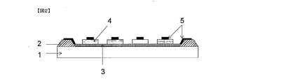
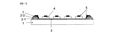
- FIG. 1 is a schematic view showing a cross section of a touch panel substrate manufactured in Example 1.
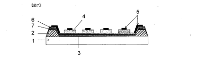
- FIG. 10 is a schematic view showing a cross section of a touch panel substrate manufactured in Example 107.
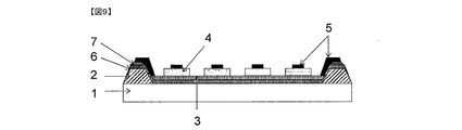
- FIG. 10 is a schematic view showing a cross section of a touch panel substrate manufactured in Example 109.
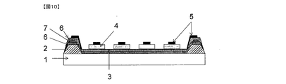
- FIG. 10 is a schematic view showing a cross section of a touch panel substrate manufactured in Example 113.
- FIG. 10 is a schematic view showing a cross section of a touch panel substrate manufactured in Example 115.
- FIG. FIG. 10 is a schematic view showing a cross section of a touch panel substrate manufactured in Example 117.
- FIG. 5 is a schematic view showing a cross section of a touch panel substrate manufactured in Example 121.
- FIG. 6 is a schematic view showing a cross section of a touch panel substrate manufactured in Example 123.
- FIG. 10 is a schematic view showing a cross section of a touch panel substrate manufactured in Example 125.
- FIG. 6 is a schematic view showing a cross section of a touch panel substrate manufactured in Example 127.
- FIG. 6 is a schematic view showing a cross section of a touch panel substrate manufactured in Example 133.
- FIG. 6 is a schematic view showing a cross section of a touch panel substrate manufactured in Example 135.
- FIG. 10 is a schematic view showing a cross section of a touch panel substrate manufactured in Example 137.
- FIG. FIG. 10 is a schematic view showing a cross section of a touch panel substrate manufactured in Example 139.
- the negative photosensitive white composition for touch panel of the present invention contains (A) a white pigment, (B) an alkali-soluble resin, (C) a polyfunctional monomer, and (D) a photopolymerization initiator.
- the negative photosensitive white composition for touch panel of the present invention contains (A) a white pigment.
- white pigment refers to an opaque pigment having no specific absorption in the visible region and having a large refractive index.
- white pigments include titanium dioxide, magnesium oxide, barium sulfate, zirconium oxide, zinc oxide, or lead white. Titanium dioxide, which has excellent shielding properties and is easily industrially used, is preferable. Surface-treated titanium dioxide for the purpose of improving dispersibility and suppressing photocatalytic activity is more preferred.
- the crystal structure of titanium dioxide includes anatase type, rutile type and brookite type. Among them, rutile type titanium oxide is preferable because it has no photocatalytic activity. Moreover, in order to improve the dispersibility in a negative photosensitive coloring composition, the light resistance of a cured film, and heat resistance, the titanium dioxide by which the surface of the particle was processed is more preferable.
- the surface treatment agent metal oxides and / or hydrates of metal oxides are preferable, and Al 2 O 3 , SiO 2 and / or ZrO 2 are more preferable. Among these, it is preferable to contain SiO 2 from the viewpoint of light resistance and heat resistance.
- the mass occupied by the surface treatment agent is preferably 10% by mass or less from the viewpoint of shielding properties.
- the average primary particle diameter of the titanium oxide is preferably 0.1 to 0.5 ⁇ m. 0.2 to 0.3 ⁇ m is more preferable. If the average primary particle size is less than 0.1 ⁇ m, the shielding property may be lowered. On the other hand, if it exceeds 0.5 ⁇ m, the white cured film may be yellowish.
- the average particle diameter of titanium dioxide which is a white pigment, is preferably 100 to 500 nm in order to improve shielding properties. In order to increase the reflectance, 170 to 310 nm is more preferable. In order to improve the light shielding property, 350 to 500 nm is more preferable.
- the average particle diameter refers to the median diameter of the particle size distribution measured by a laser diffraction method.
- the addition amount of the white pigment is preferably 10 to 80% by mass in the solid content. 20 to 70% by mass is more preferable. More preferably, it is 30 to 60% by mass. (A) If the amount of the white pigment is less than 10% by mass, sufficient shielding properties may not be obtained depending on the film thickness. On the other hand, when it exceeds 80 mass%, problems, such as a fall of chemical resistance of the obtained cured film or deterioration of pattern workability, may arise.
- the film thickness of the negative photosensitive white composition for touch panel of the present invention is preferably 10 ⁇ m or more in order to obtain light shielding properties. 15 ⁇ m or more is more preferable. More preferably, it is 20 ⁇ m or more. In this case, the crack resistance of the cured film obtained is very important.
- the thickness of the cured film can be measured with a stylus type step meter such as Surfcom 1400D (manufactured by Tokyo Seimitsu Co., Ltd.).
- the negative photosensitive white composition for touch panel of the present invention may contain a pigment dispersant in order to improve the dispersibility of (A) the white pigment.
- the pigment dispersant can be appropriately selected depending on the type of white pigment used and the surface state. It preferably contains an acidic group and / or a basic group. Examples of commercially available pigment dispersants include “Disperbyk-106”, “Disperbyk-108”, “Disperbyk-110”, “Disperbyk-180”, “Disperbyk-190”, “Disperbyk-2001”, “Disperbyk-2155”. ”,“ Disperbyk-140 ”or“ Disperbyk-145 ”(all manufactured by Big Chemie) or“ SN Dispersant 9228 ”or“ SN Sparse 2190 ”(all manufactured by Sanyo Chemical).
- the negative photosensitive white composition for a touch panel of the present invention contains (B) an alkali-soluble resin.
- the alkali-soluble resin is preferably (b-1) a siloxane resin and / or (b-2) an acrylic resin.
- b-1) a siloxane resin and / or (b-2) an acrylic resin By using (b-1) a siloxane resin and / or (b-2) an acrylic resin, a white light-shielding cured film having excellent pattern processability, high reflection strength, and little discoloration can be obtained.
- (b-1) siloxane resin is preferred.
- From the viewpoint of workability and crack resistance (b-2) acrylic resin is preferred.
- the siloxane resin is preferably a siloxane resin having a carboxyl group and / or a radical polymerizable group from the viewpoint of developability. From the viewpoint of crack resistance, siloxane resins and / or disubstituted siloxane resins having an aromatic ring are preferred. From the viewpoint of chemical resistance, a siloxane resin having an oxirane ring is preferred. From the viewpoint of reflection intensity, a siloxane resin having a fluorine group is preferred.
- alkoxysilane compound for synthesizing a siloxane resin having a carboxyl group examples include 3-trimethoxysilylpropionic acid, 3-triethoxysilylpropionic acid, 3-dimethylmethoxysilylpropionic acid, and 3-dimethylethoxysilylpropionic acid.
- the carboxylic acid equivalent of the siloxane resin having a carboxyl group is preferably 200 to 1,400 g / mol in order to balance the film thickness reduction and the development peeling.
- the carboxylic acid equivalent represents the mass of the resin necessary to obtain 1 mol of carboxyl groups, and the unit is g / mol.
- alkoxysilane compound for synthesizing a siloxane resin having a radical polymerizable group examples include vinyltrimethoxysilane, vinyltriethoxysilane, vinylmethyldimethoxysilane, vinylmethyldiethoxysilane, allyltrimethoxysilane, and allyltriethoxy.
- Silane allylmethyldimethoxysilane, allylmethyldiethoxysilane, styryltrimethoxysilane, styryltriethoxysilane, styrylmethyldimethoxysilane, styrylmethyldiethoxysilane, ⁇ -acryloylpropyltrimethoxysilane, ⁇ -acryloylpropyltriethoxysilane, ⁇ -methacryloylpropyltrimethoxysilane, ⁇ -methacryloylpropyltriethoxysilane, ⁇ -methacryloylpropylmethyldimethoxysilane, ⁇ Methacryloyl propyl methyl diethoxy silane, .gamma. acryloyl propyl methyl dimethoxy silane or .gamma. acryloyl propyl methyl diethoxy silane.
- the double bond equivalent of the siloxane resin having a radical polymerizable group is preferably 150 to 10,000 in order to balance hardness and resolution.
- the double bond equivalent represents the mass of the resin necessary to obtain 1 mol of the double bond group, and the unit is g / mol.
- alkoxysilane compound for synthesizing the siloxane resin having an aromatic ring examples include phenyltrimethoxysilane, phenyltriethoxysilane, diphenyldimethoxysilane, diphenyldiethoxysilane, 1-naphthyltrimethoxysilane, and 2-naphthyltrimethoxy.
- alkoxysilane compounds for synthesizing disubstituted siloxane resins include dimethyldimethoxysilane, dimethyldiethoxysilane, ethylmethyldimethoxysilane, ethylmethyldimethoxysilane, methylpropyldimethoxysilane, methylpropyldiethoxysilane, and diphenyldimethoxysilane.
- alkoxysilane compound for synthesizing a siloxane resin having an oxirane ring examples include 3-glycidoxypropyltrimethoxysilane, 3-glycidoxypropyltriethoxysilane, 3-glycidoxypropylmethyldimethoxysilane, 3 -Glycidoxypropylmethyldiethoxysilane, 2- (3,4-epoxycyclohexyl) ethyltrimethoxysilane, 2- (3,4-epoxycyclohexyl) ethyltriethoxysilane, 2- (3,4-epoxycyclohexyl) Ethylmethyldimethoxysilane, 2- (3,4-epoxycyclohexyl) ethylethyldimethoxysilane, 3-ethyl-3- ⁇ [3- (trimethoxysilyl) propoxy] methyl ⁇ oxetane or 3-ethyl-3- ⁇ [
- alkoxysilane compound for synthesizing a siloxane resin having a fluorine group examples include trifluoropropyltrimethoxysilane, trifluoropropyltriethoxysilane, perfluoropropyltrimethoxysilane, perfluoropropyltriethoxysilane, and perfluoropentyl.
- alkoxysilane compounds used for the synthesis of siloxane resin include, for example, methyltrimethoxysilane, methyltriethoxysilane, ethyltrimethoxysilane, ethyltriethoxysilane, propyltrimethoxysilane, propyltriethoxy Silane, isobutyltrimethoxysilane, isobutyltriethoxysilane, cyclohexyltrimethoxysilane, cyclohexyltriethoxysilane, 3-isocyanatopropyltrimethoxysilane, 3-isocyanatopropyltriethoxysilane, 3-aminopropyltrimethoxysilane, 3-aminopropyl Triethoxysilane, 3-ureidopropyltrimethoxysilane, 3-ureidopropyltriethoxysilane, tetramethoxys
- (B-1) The method of hydrolysis and condensation reaction of the alkoxysilane compound for synthesizing the siloxane resin will be described below.
- the conditions for the hydrolysis reaction for example, an acid catalyst and water are added to an alkoxysilane compound in a solvent over 1 to 180 minutes, and then the reaction is preferably performed at room temperature to 110 ° C. for 1 to 180 minutes. By performing the hydrolysis reaction under such conditions, a rapid reaction can be suppressed.
- the reaction temperature is more preferably 30 to 105 ° C.
- the hydrolysis reaction is preferably performed in the presence of an acid catalyst.
- the acid catalyst an acidic aqueous solution containing formic acid, acetic acid or phosphoric acid is preferable.
- the content of these acid catalysts is preferably 0.1 to 5 parts by mass with respect to 100 parts by mass of all alkoxysilane compounds used during the hydrolysis reaction in order to allow the reaction to proceed sufficiently.
- the conditions for the condensation reaction for example, after obtaining a silanol compound by hydrolysis of an alkoxysilane compound, the reaction solution is preferably heated as it is at 50 ° C. to the boiling point of the solvent for 1 to 100 hours.
- reheating or a base catalyst may be added.
- the produced alcohol may be distilled off by heating under reduced pressure after hydrolysis, and then a suitable solvent may be added.
- the weight average molecular weight (hereinafter referred to as “Mw”) of the siloxane resin is to improve the coating properties and the solubility in a developer when forming a pattern in terms of polystyrene measured by GPC. 2,000 to 200,000, preferably 4,000 to 20,000, more preferably 6,000 to 10,000, in order to reduce the viscosity of the negative photosensitive white composition and improve the coating uniformity. Is more preferable.
- the acrylic resin is preferably an acrylic resin containing an aromatic ring from the viewpoint of heat resistance and chemical resistance, and has a radical polymerizable group in the side chain from the viewpoint of pattern processability and crack resistance.
- An acrylic resin or an acrylic resin having a branched structure in the main chain is preferred.
- the acrylic resin refers to a polymer obtained by polymerizing methacrylic acid or a derivative thereof or acrylic acid or a derivative thereof.
- the acrylic resin containing a radical polymerizable group in the side chain was obtained by copolymerizing a (meth) acrylic monomer having a monobasic acid in the presence of a polymerization catalyst in order to improve pattern processability.
- An acrylic resin obtained by subjecting a polymer (hereinafter “base polymer”) to an addition reaction of a compound having a radical polymerizable group and an epoxy group in the molecule in the presence of an addition catalyst is preferred.
- the (meth) acrylic monomer means methacrylic acid or a derivative thereof or acrylic acid or a derivative thereof.
- Examples of the monobasic acid-containing (meth) acrylic monomer used for the synthesis of the base polymer include (meth) acrylic compounds having a carboxyl group and / or an acid anhydride group.
- Examples of the polymerization catalyst include radical polymerization initiators.
- the conditions for radical polymerization are, for example, adding (meth) acrylic monomer having a monobasic acid, other polymerizable monomers and a radical polymerization catalyst in a solvent, and sufficiently purging the reaction vessel with nitrogen by bubbling or vacuum degassing. Then, the reaction is preferably carried out at 60 to 110 ° C. for 30 to 300 minutes.
- chain transfer agents such as a thiol compound, as needed.
- Examples of the (meth) acrylic monomer having a monobasic acid used for the synthesis of the base polymer include (meth) acrylic acid, (meth) acrylic anhydride, itaconic acid, itaconic anhydride, succinic acid mono (2- (Acryloyloxyethyl), mono (2-acryloyloxyethyl) phthalate, or mono (2-acryloyloxyethyl) tetrahydrophthalate, (meth) acrylic acid is preferred from the viewpoint of developability.
- polymerizable monomers include, for example, methyl (meth) acrylate, ethyl (meth) acrylate, propyl (meth) acrylate, cyclopropyl (meth) acrylate, cyclopentyl (meth) acrylate, (meth) acrylic Cyclohexyl acid, cyclohexenyl (meth) acrylate, 4-methoxycyclohexyl (meth) acrylate, 2-cyclopropyloxycarbonylethyl (meth) acrylate, 2-cyclopentyloxycarbonylethyl (meth) acrylate, (meth) acryl 2-cyclohexyloxycarbonylethyl acid, 2-cyclohexylenylcarbonyl (meth) acrylate, 2- (4-methoxycyclohexyl) oxycarbonylethyl (meth) acrylate, norbornyl (meth) acrylate, (meth) acrylate I
- isobornyl (meth) acrylate, tricyclodecanyl (meth) acrylate, dicyclopentenyl (meth) acrylate, and styrene are preferable.
- Styrene is preferred from the viewpoint of chemical resistance.
- a methacrylic acid derivative or a styrene derivative is preferable.
- radical polymerization initiator for example, an azo compound such as azobisisobutyronitrile or an organic peroxide such as benzoyl peroxide is generally used.
- An acrylic resin having a radical polymerizable group in the side chain can be obtained by addition reaction with the compound having the above.
- the reaction conditions are, for example, a base polymer, a compound having a radical polymerizable group and an epoxy group in the molecule, a radical polymerization catalyst and a polymerization inhibitor in a solvent, and the reaction is carried out at 80 to 130 ° C. for 30 to 300 minutes. It is preferable.
- addition catalyst used in the addition reaction examples include amino catalysts such as dimethylaniline, 2,4,6-tris (dimethylaminomethyl) phenol or dimethylbenzylamine, tin (II) 2-ethylhexanoate or dibutyltin laurate.
- Tin catalyst such as titanium 2-ethylhexanoate (IV), phosphorus catalyst such as triphenylphosphine, lithium catalyst such as lithium naphthenate, zirconium catalyst such as zirconium naphthenate or naphthenic acid
- lithium catalyst such as lithium naphthenate
- zirconium catalyst such as zirconium naphthenate or naphthenic acid
- chromium-based catalysts such as chromium, acetylacetonate chromium and chromium chloride.
- a lithium catalyst, a zirconium catalyst, a chromium catalyst, or a phosphorus catalyst is preferable.
- Examples of the compound having a radical polymerizable group and an epoxy group in the molecule include glycidyl (meth) acrylate, ⁇ -ethylglycidyl (meth) acrylate, ⁇ -n-propylglycidyl (meth) acrylate, (meth ) ⁇ -n-butyl glycidyl acrylate, 3,4-epoxybutyl (meth) acrylate, 3,4-epoxyheptyl (meth) acrylate, ⁇ -ethyl-6,7-epoxyheptyl (meth) acrylate, Allyl glycidyl ether, vinyl glycidyl ether, o-vinyl benzyl glycidyl ether, m-vinyl benzyl glycidyl ether, p-vinyl benzyl glycidyl ether, ⁇ -methyl-o-vinyl benzyl
- glycidyl (meth) acrylate From the viewpoint of reactivity with a carboxyl group and from the viewpoint of developability of the resulting polymer, glycidyl (meth) acrylate, ⁇ -ethylglycidyl (meth) acrylate, ⁇ -n-propylglycidyl (meth) acrylate or (meth) ⁇ -n-Butyl glycidyl acrylate is preferred.
- Examples of the method for introducing a branched structure into the main chain of the acrylic resin include a method of polymerizing using a compound having a plurality of ethylenically unsaturated double bond groups and / or thiol groups.
- Examples of the compound having a plurality of ethylenically unsaturated double bond groups include glycerol diacrylate, glycerol dimethacrylate, glycerol acrylate methacrylate, glycerol triacrylate, glycerol trimethacrylate, glycerol diacrylate methacrylate, glycerol acrylate dimethacrylate, divinylbenzene , Trivinylbenzene, diethylene glycol diacrylate, triethylene glycol diacrylate, trimethylolpropane diacrylate or trimethylolpropane triacrylate.
- Examples of the compound having a plurality of thiol groups include pentaerythritol tetrakis (3-mercaptobutyrate), trimethylolethane tris (3-mercaptobutyrate), 1,4-bis (3-mercaptobutyryloxy) butane or 1 , 3,5-tris (3-mercaptobutyloxyethyl) -1,3,5-triazine-2,4,6 (1H, 3H, 5H) -trione.
- the unreacted thiol compound remaining in the solution after completion of the polymerization may be removed by a purification step, or may be used as the (E) thiol compound described later if not removed. The remaining amount can be calculated from 1 H-NMR.
- the Mw of the acrylic resin is preferably 2000 to 200000 in order to improve coating properties and solubility in a developing solution when forming a pattern in terms of polystyrene measured by GPC. .
- it is more preferably 4000 to 20000. More preferably, it is 6000 to 10,000.
- alkali-soluble resins include, for example, cycloolefin polymers, polyimide precursors or polyester resins.
- cycloolefin polymer examples include those obtained by addition polymerization or ring-opening metathesis polymerization of cyclohexene, norbornene, or derivatives thereof.
- a resin having an aliphatic carboxylic dianhydride and / or an aliphatic diamine as a monomer is preferable from the viewpoint of transparency.
- the polyester resin is easy to synthesize and has few side reactions, so it can be obtained by polyaddition reaction of a polyfunctional epoxy compound and a polyvalent carboxylic acid compound or polyaddition reaction of a polyol compound and a dianhydride.
- a polyol compound since a radically polymerizable group and an aromatic ring can be easily introduced, those obtained by a reaction between a polyfunctional epoxy compound and a monobasic acid compound having a radically polymerizable group are preferable.
- the negative photosensitive white composition for touch panel of the present invention contains (C) a polyfunctional monomer.
- the alkaline developer is, for example, an industrially used high-concentration developer 2.38 mass% tetramethylammonium hydroxide (TMAH) aqueous solution, 4 mass% choline aqueous solution, or low-concentration developer. 0.4% by mass TMAH aqueous solution, 0.2% by mass TMAH aqueous solution, 0.045% by mass potassium hydroxide aqueous solution, 1% by mass sodium hydrogen carbonate aqueous solution, 0.2% by mass sodium hydrogen carbonate solution or 0.1% by mass water A sodium oxide aqueous solution is mentioned.
- TMAH tetramethylammonium hydroxide
- R 1 independently represents hydrogen, a methyl group, an ethyl group, a propyl group, or a phenyl group, and n represents an integer of 1 to 30.
- R 1 in the general formula (1) is preferably a hydrogen atom or a methyl group from the viewpoint of solubility in an alkali developer.
- the double bond equivalent of the polyfunctional monomer is preferably 800 g / mol or less, more preferably 500 g / mol or less, and further preferably 300 g / mol or less from the viewpoint of curability during light irradiation.
- the polyfunctional monomer (C) having the structure represented by the general formula (1) for example, a polyol obtained by reacting a compound having a plurality of active hydrogens or a halide thereof with various alkylene oxides.
- the method of making a compound react with (meth) acrylic acid further is mentioned.
- Examples of the compound having a plurality of active hydrogens include, for example, alcohol compounds such as ethylene glycol, propylene glycol, butylene glycol, glycerin, trimethylolpropane, pentaerythritol, dipentaerythritol, tripentaerythritol or hexanediol, bisphenol A, bisphenol E Phenol compounds such as bisphenol F, bisphenol S or 9,9- (4-hydroxyphenyl) fluorene, amide compounds such as isocyanuric acid, pentaerythritol tetrakis (3-mercaptobutyrate), trimethylolpropane tris (3-mercaptobutyrate) Rate), tris (3-mercaptobutyrate) ethoxyisocyanurate, 1,2-ethanedithiol, or 1,2 propanedithiol Thiol compounds such Lumpur like.
- alcohol compounds such as ethylene glycol, propylene glycol, buty
- an aliphatic compound such as ethylene glycol, propylene glycol, glycerin or trimethylolpropane is preferred.
- Isocyanuric acid is preferred from the viewpoint of crack resistance.
- alkylene oxide include ethylene oxide, propylene oxide, and butylene oxide.
- Examples of the method for synthesizing the (C) polyfunctional monomer having the structure represented by the general formula (2) include a compound having a plurality of glycidyl ether groups, or a compound having a glycidyl ether group and a radical polymerizable group, The method of making it react with (meth) acrylic acid is mentioned.
- Examples of the compound having a plurality of glycidyl ether groups include ethylene glycol diglycidyl ether, propylene glycol diglycidyl ether, diethylene glycol diglycidyl ether, dipropylene glycol diglycidyl ether, triethylene glycol diglycidyl ether, tripropylene glycol diglycidyl ether, Tetraethylene glycol diglycidyl ether, tetrapropylene glycol diglycidyl ether, polyethylene glycol 200-diglycidyl ether, polyethylene glycol 300-diglycidyl ether, polyethylene glycol 400-diglycidyl ether, bisphenol A diglycidyl ether or bisphenol F diglycidyl ether, Bisphenol E From the viewpoint of developability, ethylene glycol diglycidyl ether, propylene glycol diglycidyl ether, diethylene glycol diglycidyl ether, dipropylene glycol diglycidyl ether, triethylene
- Examples of the compound having a glycidyl ether group and a radical polymerizable group include glycidyl (meth) acrylate, ⁇ -ethylglycidyl (meth) acrylate, ⁇ -n-propylglycidyl (meth) acrylate, and (meth) acrylic acid.
- Examples of the (C) polyfunctional monomer having the structure represented by the general formula (1) and / or the (C) polyfunctional monomer having the structure represented by the general formula (2) include, for example, ethylene glycol diglycidyl. Ether (meth) acrylate, propylene glycol diglycidyl ether (meth) acrylate, diethylene glycol diglycidyl ether (meth) acrylate, dipropylene glycol diglycidyl ether (meth) acrylate, triethylene glycol diglycidyl ether (meth) acrylate, tripropylene glycol Diglycidyl ether (meth) acrylate, tetraethylene glycol diglycidyl ether (meth) acrylate, tetrapropylene glycol diglycidyl ether (meth) acrylate, polyethylene Recall 200-diglycidyl ether (meth) acrylate, polyethylene glycol 300-diglycidyl ether (meth) acrylate, poly
- Examples of other (C) polyfunctional monomers include 1,4-butanediol di (meth) acrylate, 1,5-pentanediol di (meth) acrylate, 1,6-hexanediol di (meth) acrylate, 1 , 9-nonanediol di (meth) acrylate, tricyclododecane di (meth) acrylate, pentaerythritol tetra (meth) acrylate, dipentaerythritol hexa (meth) acrylate, dipentaerythritol penta (meth) acrylate, tripentaerythritol hepta (Meth) acrylate, tripentaerythritol octa (meth) acrylate, pentaerythritol tri (meth) acrylate succinic acid adduct or dipentaerythritol penta (meth
- the content of the polyfunctional monomer is not particularly limited, but is preferably 20 to 70% by mass in the solid content from the viewpoint of developability, photocurability and heat resistance. If it is less than 20% by mass, the crosslinking reaction at the time of exposure may not proceed sufficiently, and if it exceeds 70% by mass, the film strength after coating (before exposure) may be reduced, causing a problem in the process. There is.
- the negative photosensitive white composition for a touch panel of the present invention contains (D) a photopolymerization initiator.
- a photopolymerization initiator refers to one that decomposes and / or reacts with light (including ultraviolet rays and electron beams) to generate radicals.
- Examples of (D) photopolymerization initiators include 2-methyl-1- (4-methylthiophenyl) -2-morpholinopropan-1-one, 2-benzyl 2-dimethylamino-1- (4-morpholino Phenyl) -butan-1-one, 2- (dimethylamino) -2-[(4-methylphenyl) methyl] -1- [4- (4-morpholinophenyl) -butan-1-one, 2,4 , 6-trimethylbenzoylphenylphosphine oxide, bis (2,4,6-trimethylbenzoyl) -phenylphosphine oxide, bis (2,6-dimethoxybenzoyl)-(2,4,4-trimethylpentyl) -phosphine oxide, 1 , 2-octanedione, 1- [4- (phenylthio) -2- (O-benzoyloxime)], ethanone, 1- [9-ethyl- -(2-Methyl
- 2,4,6-trimethylbenzoylphenylphosphine oxide bis (2,4,6-trimethylbenzoyl) -phenylphosphine oxide or bis (2,6-dimethoxybenzoyl)-(2, Acylphosphine oxide photopolymerization initiators such as 4,4-trimethylpentyl) -phosphine oxide are preferred.
- the negative photosensitive white composition for touch panel of the present invention preferably contains (E) a thiol compound.
- E By containing the thiol compound, the taper shape of the pattern edge becomes gentle. Moreover, adhesiveness with glass can be improved and development peeling can be suppressed. Furthermore, the tolerance with respect to the chemical
- the addition amount of the thiol compound is preferably 0.3 to 20 parts by mass, and 0.5 to 15 parts by mass with respect to a total of 100 parts by mass of (B) alkali-soluble resin and (C) polyfunctional monomer. More preferred is 1 to 10 parts by mass, still more preferred is 2 to 8 parts by mass.
- the thiol compound is preferably a polyfunctional thiol from the viewpoint of suppressing development peeling.
- a monofunctional thiol it is preferable to contain a reactive functional group in the molecule.
- the monofunctional thiol containing a reactive functional group in the molecule has a reactive functional group, so that it can be reacted during the pre-baking step and function substantially as a polyfunctional thiol.
- the reactive functional group include an isocyanate group, an alkoxysilyl group, a methylol group, a (meth) acryloyl group, an epoxy group, an oxetanyl group, a furyl group, and a vinyl group.
- the number of functional groups per molecule of the polyfunctional thiol compound is preferably 2 to 8, and more preferably 3 to 6.
- the thiol compound is preferably an ester compound of a polyhydric alcohol compound and a secondary or tertiary mercapto group-containing carboxylic acid compound from the viewpoint of the storage stability of the composition. All the compounds obtained are polyfunctional thiols.
- polyhydric alcohol compound examples include alkylene glycol (wherein the alkylene group has 2 to 10 carbon atoms and may be branched), diethylene glycol, dipropylene glycol, glycerin, trimethylolpropane, tris ( 2-hydroxyethyl) isocyanurate, pentaerythritol or dipentaerythritol.
- alkylene glycol wherein the alkylene group has 2 to 10 carbon atoms and may be branched
- diethylene glycol dipropylene glycol
- glycerin trimethylolpropane
- tris ( 2-hydroxyethyl) isocyanurate pentaerythritol or dipentaerythritol.
- secondary or tertiary mercapto group-containing carboxylic acid compound examples include 2-mercaptopropionic acid, 3-mercaptobutanoic acid, 2-mercaptoisobutanoic acid, 4-mercaptopentanoic acid, and 3-
- polyfunctional thiols examples include pentaerythritol tetrakis (2-mercaptopropionate), trimethylolpropane tris (2-mercaptopropionate), trimethylolethane tris (2-mercaptopropionate), and glycerin tris.
- Examples of other thiol compounds include 1,4-butanedithiol, 1,5-pentanedithiol, 1,6-hexanedithiol, 1,9-nonanedithiol, pentaerythritol tetrakis (3-mercaptopropionate), tri Methylolpropane tris (3-mercaptopropionate), trimethylolethane tris (3-mercaptopropionate), glycerol tris (3-mercaptopropionate), tris (3-mercaptopropionate) ethoxyisocyanurate, ethylene Glycol bis (3-mercaptopropionate), 1,2-propylene glycol (3-mercaptopropionate), 1,4-butylene glycol (3-mercaptopropionate), diethylene glycol bis (3-mercapto Propionate) or dipropylene glycol bis (3-mercaptopropionate) multifunctional thiol or 3-mercaptopropionic acid or 3-mercaptoprop
- the negative photosensitive white composition for touch panel of the present invention may contain (F) an antioxidant.
- an antioxidant By containing antioxidant, yellowing after the heat processing of a post process is suppressed.
- a hindered phenol-based antioxidant or a hindered amine-based antioxidant having an Mw of 300 or more is preferable because it is excellent in the effect of suppressing discoloration of the cured film. If Mw is less than 300, it may sublime at the time of thermosetting, and a sufficient antioxidant effect may not be obtained. Further, the amount of the phenol group or amino group in one molecule is preferably 2 or more and more preferably 4 or more because an antioxidant effect is easily obtained.
- hindered phenol antioxidant examples include okdadecyl 3- (3,5-di-t-butyl-4-hydroxyphenyl) propionate, hexamethylene bis [3 (3,5-di-t-butyl-4 -Hydroxyphenylpropionate, thiodiethylenebis [3 (3,5-di-t-butyl-4-hydroxyphenylpropionate, ethylenebis (oxyethylene) bis (3- (5-t-butyl-4-hydroxy- m-tolyl) propionate, tris- (3,5-di-t-butyl-4-hydroxybenzyl) -isocyanurate, 1,3,5-trimethyl-2,4,6-tris (3,5-di-) t-butyl-4-hydroxybenzyl) benzene, pentaerythritol tetrakis (3- (3,5-di-t-butyl-4-hydroxyphenyl) Nyl) propionate, 2-t-but-
- hindered amine compound examples include bis (1,2,2,6,6-pentamethyl-4-piperidyl) [[3,5-bis (1,1-dimethylethyl) -4-hydroxyphenyl] methyl] butylmalo.
- the addition amount of the antioxidant is preferably 0.2 to 4.0 parts by mass with respect to 100 parts by mass in total of (B) the alkali-soluble resin and (C) the polyfunctional monomer, and 0.3 More preferred is 2.0 parts by mass. If the addition amount is less than 0.3 parts by mass, it is difficult to obtain the effect of suppressing discoloration, and if it exceeds 4.0 parts by mass, the exposed portion may be hardened and pattern processing may not be possible.
- the negative photosensitive white composition for a touch panel of the present invention may contain a (G) silane coupling agent represented by the general formula (3).
- R 2 independently represents an alkyl group having 1 to 6 carbon atoms or a substituent thereof, l represents 0 or 1
- R 3 represents a trivalent organic group having 3 to 30 carbon atoms
- R 4 each independently represents an alkyl group having 1 to 6 carbon atoms, an alkoxy group having 1 to 6 carbon atoms, a phenyl group or a phenoxy group, or a substituted product thereof.
- G By containing the silane coupling agent represented by General formula (3), the adhesiveness to the board
- R ⁇ 2 > in General formula (3) a methyl group, an ethyl group, or a butyl group is preferable, and a methyl group or an ethyl group is more preferable from a viewpoint of raw material acquisition.
- R 3 in the general formula (3) is preferably an alkyl group, and more preferably an alkyl group having 3 to 10 carbon atoms from the viewpoint of solubility in an organic solvent.
- Examples of the (G) silane coupling agent represented by the general formula (3) include 3- (tert-butylcarbamoyl) -6- (trimethoxysilyl) hexanoic acid, 2- (2- (tert-butyl).
- the negative photosensitive white composition for touch panel of the present invention may contain (H) an ultraviolet absorber.
- an ultraviolet absorber By containing an ultraviolet absorber, the resolution is improved and the light resistance of the resulting cured film is improved.
- an ultraviolet absorber a benzotriazole compound, a benzophenone compound, or a triazine compound is preferable from the viewpoints of transparency and non-colorability.
- benzotriazole compounds examples include 2- (2H benzotriazol-2-yl) phenol, 2- (2H-benzotriazol-2-yl) -4,6-tert-pentylphenol, and 2- (2H benzotriazole).
- examples of the ultraviolet absorber of the benzophenone compound examples include 2-hydroxy-4-methoxybenzophenone.
- Examples of the ultraviolet absorber of the triazine compound examples include 2- (4,6-diphenyl-1,3,5 triazin-2-yl) -5-[(hexyl) oxy] -phenol.
- the negative photosensitive white composition for touch panel of the present invention may contain (I) a colorant to the extent that whiteness is not impaired.
- a colorant to the extent that whiteness is not impaired.
- the white cured film which exhibited various colors, such as yellowishness, redness, or blueness, can be obtained. On the contrary, it is also possible to shift the colored white cured film to White Point.
- a coloring agent dye, an organic pigment, or an inorganic pigment is mentioned, for example. Of these, inorganic pigments are preferred from the viewpoint of heat resistance.
- organic pigment examples include Pigment Yellow 12, 13, 17, 20, 24, 83, 86, 93, 95, 109, 110, 117, 125, 129, 137, 138, 139, 147, 148, 150, 153.
- Yellow organic pigments such as 154, 166, 168 or 185, orange organic pigments such as pigment orange 13, 36, 38, 43, 51, 55, 59, 61, 64, 65 or 71, pigment red 9, 48, Red organic pigments such as 97, 122, 123, 144, 149, 166, 168, 177, 179, 180, 192, 209, 215, 216, 217, 220, 223, 224, 226, 227, 228, 240 or 254 Pigment Violet 19, 23, 29, 30, 32, 37, 40 or 50 Purple organic pigments, blue organic pigments such as pigment blue 15, 15: 3, 15: 4, 15: 6, 22, 60 or 64, green organic pigments such as pigment green 7, 10 or 36, or carbon Examples thereof include black organic pigments such as black, perylene
- Pigment Blue 15 3
- Pigment Blue 15: 4 Pigment Blue 15: 6, Pigment Green 7, Pigment Green 36, or carbon black
- These organic pigments may be subjected to surface treatment such as rosin treatment, acidic group treatment, or basic treatment, if necessary.
- the addition amount of the organic pigment is preferably 50 to 5000 ppm from the viewpoint of whiteness.
- inorganic pigments examples include metal oxides such as iron oxide, cadmium sulfide, titanium nickel antimony, titanium nickel barium, strontium chromate, viridian, chromium oxide, cobalt aluminate or titanium nitride, metal oxides, composite oxides, metals Sulfides, metal nitrides or metal oxynitrides are mentioned.
- These inorganic pigments may be surface-treated with other inorganic components or organic components. From the viewpoint of heat resistance, it is preferable that the surface is treated with another inorganic component.
- the addition amount of the inorganic pigment is preferably 50 to 5000 ppm (mass ratio) with respect to the solid content from the viewpoint of whiteness.
- the dye examples include an anthraquinone series, a perinone series, a perylene series, a disazo series, a quinoline series, a methine series, a monoazo series, a xanthene series or a phthalocyanine series compound, a red series dye, a blue series dye, a yellow series dye, or the like.
- examples include green dyes.
- red dyes include Solvent RED 8, 52, 111, 135, 168, 179, 207, 218 or 246 (all numerical values are color index (CI) numbers; the same applies hereinafter). Solvent RED 179 or 218 is preferable from the viewpoint of heat resistance.
- Examples of blue dyes include Solvent BLUE 35, 36, 44, 63, 78, 94, or 97.
- Examples of yellow dyes include Solvent YELLOW 16, 33, 88 or 93.
- Examples of the green dye include Solvent GREEN 3 or 20.
- the addition amount of the dye is preferably 5 to 500 ppm (mass ratio) with respect to the solid content from the viewpoint of whiteness.
- the negative photosensitive white composition for touch panel of the present invention may contain an organic solvent.
- the organic solvent is preferably an alcoholic compound, an ester compound or an ether compound in order to uniformly dissolve each component of the composition. From the viewpoint of pigment dispersibility, ester compounds or ether compounds are more preferable.
- a compound having a boiling point of 110 to 250 ° C. under atmospheric pressure is preferred. Since the negative photosensitive white composition for touch panel of the present invention is assumed to be applied by a printing method such as spin coater, slit coater, screen printing, ink jet, gravure printing or bar coater, the boiling point is less than 110 ° C. In addition, the drying speed of the organic solvent is fast, and defects in coating uniformity are likely to occur. On the other hand, when the boiling point exceeds 250 ° C., the organic solvent remains in the obtained cured film, and the heat resistance of the cured film is deteriorated.
- organic solvent examples include propylene glycol monomethyl ether, propylene glycol monomethyl ether acetate, diacetone alcohol, tetrahydrofurfuryl alcohol, ethylene glycol mononormal butyl ether, 2-ethoxyethyl acetate, 1-methoxypropyl-2-acetate, 3- Methoxy-3-methylbutanol, 3-methoxy-3-methylbutanol acetate, 3-methoxybutyl acetate, 1,3-butylene glycol diacetate, ethylene glycol monobutyl ether acetate, diethylene glycol monobutyl ether acetate, ethyl lactate, butyl lactate, aceto Examples include ethyl acetate or ⁇ -butyrolactone.
- the solid content concentration of the negative photosensitive white composition for touch panel of the present invention is preferably 40% by mass or more, more preferably 50% by mass or more because thick film processing becomes easy. Moreover, 75 mass% or less is preferable from a viewpoint of viscosity control, and 65 mass% or less is more preferable.
- the viscosity of the negative photosensitive white composition for a touch panel of the present invention is preferably 15 cP or less, more preferably 10 cP or less, because application control with a slit coater becomes easy.
- Examples of the method for measuring the viscosity include a narrow tube type, a falling ball type, and a rotary type, and a rotary type capable of highly accurate measurement is preferable.
- Examples of the rotary viscometer include a single cylindrical rotary (B type) viscometer and a cone plate (E type) viscometer. A total is preferred.
- Examples of the method for setting the viscosity to 15 cP or less at a solid content concentration of 40 to 75% by mass include a method in which the addition amount of (B) alkali-soluble resin is 20% by mass or less in the solid content. Moreover, even when the addition amount of (B) alkali-soluble resin exceeds 20 mass% in solid content, it becomes achievable by making Mw of (B) alkali-soluble resin into 20000 or less.
- the negative photosensitive white composition for touch panel of the present invention may contain a surfactant in order to improve applicability.
- a surfactant include a fluorine-based surfactant, a silicone-based surfactant, a polyalkylene oxide-based surfactant, and a poly (meth) acrylate-based surfactant.
- a typical production method of the negative photosensitive white composition for touch panel of the present invention will be described below.
- a mixed liquid of (A) a white pigment, (B) an alkali-soluble resin and an organic solvent is dispersed using a mill type disperser filled with zirconia beads to obtain a pigment dispersion.
- (B) alkali-soluble resin, (C) polyfunctional monomer, (D) photopolymerization initiator, organic solvent and other additives are dissolved by stirring to obtain a diluted solution.
- a negative photosensitive white composition is obtained by mixing, stirring, and filtering a dispersion liquid and a dilution liquid.
- the negative photosensitive white composition for a touch panel of the present invention is applied on a base substrate by a spin coater, slit coater, screen printing, ink jet or bar coater, etc., using a heating device such as a hot plate or oven, Pre-bake at 60 to 150 ° C. for 30 seconds to 3 minutes.
- the film thickness after pre-baking is preferably 10 to 30 ⁇ m.
- light with an exposure intensity of about 10 to 4000 J / m 2 (wavelength 365 nm exposure dose conversion) are exposed through irradiation with or without a desired mask.
- the exposure light source include ultraviolet rays such as i-line, g-line, and h-line, KrF (wavelength 248 nm) laser, and ArF (wavelength 193 nm) laser.
- a negative pattern can be obtained by dissolving the exposed portion by development.
- a developing method it is preferable to immerse in a developer for 5 seconds to 10 minutes by a method such as shower, dipping or paddle.
- the developer include inorganic alkalis such as alkali metal hydroxides, carbonates, phosphates, silicates and borates, amines such as 2-diethylaminoethanol, monoethanolamine and diethanolamine, or tetramethyl
- An aqueous solution of a quaternary ammonium salt such as ammonium hydroxide (TMAH) or choline can be used.
- TMAH ammonium hydroxide
- the developed film is heated at 120 to 250 ° C. for 15 minutes to 2 hours using a heating device such as a hot plate or an oven to obtain a white light-shielding cured film.
- the cured film obtained by curing the negative photosensitive white composition for a touch panel of the present invention is suitable as a light shielding pattern in an OGS type touch panel.
- the OD value (Optical Density) of the light shielding pattern is preferably 0.6 or more, and more preferably 0.7 or more.
- the total reflection of the light-shielding pattern (incident angle 8 °, light source: D-65 (2 ° field of view)) is 70 ⁇ L * ⁇ 99, ⁇ 5 in the CIE 1976 (L *, a *, b *) color space, respectively.
- ⁇ b * ⁇ 5 and ⁇ 5 ⁇ a * ⁇ 5 are preferable, and 80 ⁇ L * ⁇ 99, ⁇ 2 ⁇ b * ⁇ 2, and ⁇ 2 ⁇ a * ⁇ 2 are more preferable.
- ⁇ b * ⁇ 5 and ⁇ 5 ⁇ a * ⁇ 5 are preferable, and 80 ⁇ L * ⁇ 99, ⁇ 2 ⁇ b * ⁇ 2, and ⁇ 2 ⁇ a * ⁇ 2 are more preferable.
- the touch panel which comprises a white light-shielding cured film pattern can be manufactured by passing through the process of forming a white light-shielding cured film pattern using the negative photosensitive white composition for touch panels of this invention.
- a manufacturing method thereof a method of forming a transparent electrode, an insulating film, and a metal wiring after forming a white light-shielding cured film pattern is common, and a protective film may be formed as necessary.
- Examples of the method for forming the transparent electrode include a method of forming a film of ITO by a sputtering method and then patterning through a photoresist process, an etching process, and a peeling process.
- Examples of the method for forming the metal wiring include a method in which copper or MAM (molybdenum / aluminum / molybdenum laminated film) is formed by vapor deposition or sputtering, and then patterned through a photoresist process, an etching process, and a peeling process. It is done. Moreover, the method of forming a silver paste by printing or the lithography method is also mentioned.
- MAM mobdenum / aluminum / molybdenum laminated film
- a transparent and excellent insulating material is preferable.
- a transparent inorganic film or a transparent resin film examples include a transparent inorganic film or a transparent resin film.
- the method for forming the transparent inorganic film include a method of forming a silicon oxide or silicon nitride thin film by a CVD (Chemical Vapor Deposition) method.
- the method for forming the transparent resin film include a method using a lithography method using a negative or positive photosensitive transparent resin composition.
- the negative photosensitive transparent resin composition examples include a composition containing an alkali-soluble resin, a polyfunctional monomer, and a photopolymerization initiator. You may use an additive as needed.
- the positive photosensitive transparent resin composition examples include a composition containing an alkali-soluble resin and a quinonediazide compound. You may use an additive as needed.
- a compound in which naphthoquinonediazidesulfonic acid is ester-bonded to a compound having a phenolic hydroxyl group is preferable.
- a compound in which naphthoquinone diazide is ester-bonded to a compound having a phenolic hydroxyl group can be obtained by esterifying a compound having a phenolic hydroxyl group and naphthoquinone diazide sulfonic acid chloride by a known method.
- Examples of the compound having a phenolic hydroxyl group include the following compounds (trade name, manufactured by Honshu Chemical Industry Co., Ltd.).
- naphthoquinone diazide sulfonic acid examples include 4-naphthoquinone diazide sulfonic acid and 5-naphthoquinone diazide sulfonic acid. Since 4-naphthoquinonediazide sulfonic acid ester compound has absorption in the i-line (wavelength 365 nm) region, it is suitable for i-line exposure. Further, the 5-naphthoquinonediazide sulfonic acid ester compound has absorption in a wide wavelength range and is therefore suitable for exposure in a wide wavelength range.
- 4-naphthoquinone diazide sulfonic acid ester compound it is preferable to select either 4-naphthoquinone diazide sulfonic acid ester compound or 5-naphthoquinone diazide sulfonic acid ester compound depending on the wavelength to be exposed.
- a 4-naphthoquinone diazide sulfonic acid ester compound and a 5-naphthoquinone diazide sulfonic acid ester compound may be mixed and used.
- the molecular weight of the naphthoquinone diazide compound is preferably 300 to 1500, and more preferably 350 to 1200. If the molecular weight of the naphthoquinone diazide compound exceeds 1500, pattern formation may not be possible with an addition amount of 4 to 10% by mass. On the other hand, when the molecular weight is less than 300, the colorless transparency may be lowered.
- the step of forming the white light-shielding cured film using the negative photosensitive white composition for touch panel of the present invention may be repeated a plurality of times.
- By laminating and forming a cured film thinner than the target film thickness both high resolution and low taper can be achieved at a high level.
- the taper shape can be easily controlled. Therefore, when the process of forming the white light-shielding cured film pattern is repeated n times, the nth layer (n is an integer of 2 or more) ) Is preferably wider than the n-1th layer, and the film thickness is preferably thin.
- the process of forming a white light-shielding cured film using the negative photosensitive white composition for touch panel of the present invention can be combined with a printing process using a non-photosensitive white ink composition.
- a non-photosensitive white ink composition having high heat resistance using a siloxane resin.
- siloxane resin for example, in addition to the preferred siloxane resin described above, commercially available products include “804 RESIN”, “805 RESIN”, “806 RESIN”, “806A RESIN”, “840 RESIN”, “SR-2400”.
- silicone resins such as “KR-282”, “KR-311”, and “KR-211” (manufactured by Shin-Etsu Chemical Co., Ltd.).
- a negative photosensitive white composition for touch panel of the present invention is used, and after processing with a thin film in a necessary area, a slightly small pattern is processed to be thick on the upper surface by printing.
- a screen area and a fine pattern area periphery using a negative photosensitive white composition the structure which processes other required areas is mentioned. Thereby, excellent pattern processability (high resolution, high linearity, etc.) and whiteness can be achieved at a high level.
- a black light-shielding cured film may be formed on the white light-shielding cured film formed using the negative photosensitive white composition for touch panel of the present invention.
- the OD value can be improved and the visibility of the metal wiring formed thereon can be lowered.
- a method for forming the black light-shielding cured film for example, a lithography method using a photosensitive black resin composition is preferable from the viewpoint of resolution.
- Examples of the photosensitive black resin composition include a composition containing a black pigment, an alkali-soluble resin, a polyfunctional monomer, and a photopolymerization initiator. You may use an additive as needed.
- Examples of the black pigment include carbon black and titanium nitride.
- a transparent film may be formed on the white light-shielding cured film formed using the negative photosensitive white composition for touch panel of the present invention.
- the transparent film may be formed on the entire substrate or only on the light shielding pattern.
- the transparent film can be formed by, for example, the same material and processing method as the above insulating film and protective film.
- a color adjustment layer may be formed on the upper and / or lower part of the white light-shielding cured film formed using the negative photosensitive white composition for touch panel of the present invention.
- various colors such as yellow, red or blue can be imparted to the appearance of the white pattern from the back surface.
- the transmitted light (light source: D-65 (2 ° field of view) CIE1976 (L *, a *, b *) of the color adjustment layer is 70 in each color space.
- the color adjustment layer is formed on the white light-shielding cured film, the total reflection ( The incident angle is 8 ° and the light source is D-65 (2 ° field of view), preferably 10 ⁇ L * ⁇ 70, ⁇ 50 ⁇ b * ⁇ 50, and ⁇ 50 ⁇ a * ⁇ 50.
- the color adjusting layer is preferably lower than the black light-shielding cured film, and if formed on the upper part, the color adjusting function may be lowered. Examples of the method include a lithography method using a photosensitive colored resin composition from the viewpoint of resolution. Masui.
- the photosensitive colored resin composition examples include a composition containing a colorant, an alkali-soluble resin, a polyfunctional monomer, and a photopolymerization initiator, but additives may be used as necessary.
- the colorant include the above-described dyes, organic pigments, and inorganic pigments.
- the content of the colorant is preferably 5% by mass to 40% by mass of the whole solid part when formed on the upper part of the white light-shielding cured film, and 0.0005 to 1% by mass of the whole solid part when formed on the lower part. % Is preferable because it easily satisfies the optical characteristics described above.
- aqueous phosphoric acid solution in which 0.372 g of phosphoric acid (0.2% by mass relative to the charged monomer) was dissolved in 56.7 g of water was added with a dropping funnel over 10 minutes. After stirring at 40 ° C. for 1 hour, the oil bath temperature was set to 70 ° C. and stirred for 1 hour, and the oil bath was further heated to 115 ° C. over 30 minutes. One hour after the start of temperature increase, the internal temperature of the solution reached 100 ° C., and was then heated and stirred for 2 hours (the internal temperature was 100 to 110 ° C.). During the reaction, methanol and water as by-products were distilled off using a Liebig cooling device.
- PGMEA was added to the obtained polysiloxane PGMEA solution so that the polymer concentration was 40% by mass to obtain a siloxane resin solution (B1).
- Mw of the obtained polymer was measured by GPC, it was 6000 (polystyrene conversion).
- TCDMA Tricyclo [5.2.1.02,6] decan-8-yl methacrylate
- GMA glycidyl methacrylate
- Cr (AcAc) 3 chrome acetylacetonate
- PGMEA p-Methoxyphenol
- a polymer containing MA unit is first polymerized, and then an epoxy group of GMA and a carboxylic acid derived from MA unit are reacted.
- the unit in which the MA unit and GMA reacted is represented by “MA-GMA” in the table.
- Table 2 shows unit ratios of the obtained acrylic resin solutions (B8) to (B16).
- the obtained solution was diluted with PGMEA so that the solid content concentration was 20% by mass, and 3- (tert-butylcarbamoyl) -6- (trimethoxysilyl) hexanoic acid, 2- (2- (tert-butyl) was obtained.
- a mixed solution (G1) of amino) -2-oxoethyl) -5- (trimethoxysilyl) pentanoic acid was obtained.
- Negative photosensitive white compositions were prepared in the same manner as in Preparation Example 1 at the ratios shown in Table 3, Table 4, Table 5, and Table 6.
- CR-97 Titanium dioxide pigment (alumina / zirconia coating, manufactured by Ishihara Sangyo Co., Ltd.)
- JR-605 Titanium dioxide pigment (alumina coating, manufactured by Teika Industry Co., Ltd.)
- R960 Titanium dioxide pigment (alumina / silica coating, manufactured by DuPont)
- MT-PE1 pentaerythritol tetrakis (3-mercaptobutyrate) (manufactured by Showa Denko KK)
- MT-BD1 1,4-butylene glycol (3-mercaptobutyrate) (manufactured by Showa Denko KK)
- MT-NR1 Tris (3-mercaptobutyryloxyethyl) isocyanurate (manufactured by Showa Denko KK) ⁇
- TPMB Trimethylolpropane tris (3-mercaptobutyrate) (manufactured by Showa Denko KK)
- TEMB Tri
- the blue material dispersion DB-1 is the same as the black material dispersion DBk-1, except that the blue organic pigment PB15: 6 (manufactured by Toyo Ink Co., Ltd.) is used instead of the black pigment Irgaphor Black S0100CF as the colorant. Got.
- the blue material dispersion DB-2 is the same as the black material dispersion DBk-1, except that the blue inorganic pigment PB28 (manufactured by Dainichi Seika Kogyo Co., Ltd.) is used in place of the black pigment Irgaphor Black S0100CF as the colorant. Got.
- V-1) Preparation Example 112 Preparation of Negative Photosensitive Coloring Composition (V-1)
- a negative photosensitive coloring composition (Bk-1) was prepared in the same manner as in the preparation of the negative photosensitive black composition (Bk-1) except that the purple material dispersion DV-1 was used instead of the black material dispersion DBk-1. V-1) was obtained.
- Example 1 The negative photosensitive white composition (W-1) obtained in Preparation Example 1 was evaluated for physical properties by the following methods (i) to (vi), and the touch panel was tested by the following (vii) method. Evaluation on manufacturing was carried out.
- PLA PLA-501F; manufactured by Canon Inc.
- an ultrahigh pressure mercury lamp as a light source
- a mask having a 150 ⁇ m wide line & space pattern an exposure amount of 200 mJ (i line), a mask gap Exposure was at 150 ⁇ m.
- an automatic developing device manufactured by Takizawa Sangyo Co., Ltd .; AD-2000
- TMAH aqueous solution ELM-D; manufactured by Mitsubishi Gas Chemical Co., Ltd.
- 0.045 mass% KOH aqueous solution shower developed for 60 seconds, then rinsed with water for 30 seconds.
- Extractability S There is no residue in the linear pattern with a line width of 100 ⁇ m.
- A There is a residue in the extraction pattern with a linear line width of 100 ⁇ m, but there is no residue in the extraction pattern with a line width of 150 ⁇ m.
- B Although there is a residue in a linear pattern with a line width of 150 ⁇ m, there is no residue in a pattern with a line width of 200 ⁇ m.
- C There is a residue in a linear pattern with a line width of 200 ⁇ m.
- A The exposed portion of L / S with a width of 100 ⁇ m or more remains without peeling from the substrate, but the L / S with a width of 100 ⁇ m or less is peeled off.
- B An exposed portion of L / S having a width of 150 ⁇ m or more remains without being peeled from the substrate, but L / S having a width of 150 ⁇ m or less is peeled off.
- C An exposed portion of L / S having a width of 150 ⁇ m or more is peeled off from the substrate.
- the evaluation of the development adhesiveness was performed when the detachability was “S, A, B”.
- C Undercut shape (iii) Evaluation of adhesiveness
- Pre-baking was performed at 100 ° C. for 3 minutes using a hot plate to form a coating film having a thickness of 15 ⁇ m.
- the entire surface of the substrate was exposed using PLA with an ultrahigh pressure mercury lamp as a light source.
- shower development was performed for 120 seconds with a 2.38 mass% TMAH aqueous solution or 0.045 mass% KOH aqueous solution, and then rinsed with water for 30 seconds.
- a cured film was formed by curing for 30 minutes at 230 ° C. in air using an oven.
- JIS S6050 passed product
- each white cured film was sequentially subjected to chemical treatment under the following conditions (1) to (3), and then evaluated for adhesiveness in the same manner as (iii) above.
- the rinse by the pure water shower for 30 seconds was implemented between each chemical
- Chemical resistance was evaluated based on the following criteria.
- Adhesive evaluation after chemical treatment with white cured film alone is 4-5.
- ⁇ Eab (X1 ⁇ 2 + X2 ⁇ 2 + X3 ⁇ 2) ⁇ 0.5 (2) here, X1: ⁇ L * (0) ⁇ - ⁇ L * (1) ⁇ X2: ⁇ a * (0) ⁇ - ⁇ a * (1) ⁇ X3: ⁇ b * (0) ⁇ - ⁇ b * (1) ⁇ L * (0), a * (0), and b * (1) ⁇ L * (0), a * (0), and b * (1) ⁇ L * (0), a * (0), and b * (1) ⁇ L * (0), a * (0), and b * (1) respectively indicate the values of L *, a *, and b * of the cured film for film property evaluation, and L * (1) , A * (1), b * (1) respectively indicate the values of L *, a *, and b * of the cured film subjected to additional heat treatment.
- a touch panel substrate was produced by the following procedure.
- the resulting film was subjected to pattern exposure with an ultra-high pressure mercury lamp through a mask, followed by shower development with a 2.38 mass% TMAH aqueous solution for 90 seconds using an automatic developing device, and then rinsed with water for 30 seconds. . Thereafter, the ITO is etched by immersing in a 3.5% by mass oxalic acid aqueous solution for 150 seconds, and the photoresist is removed by treating with a stripping solution (4% potassium hydroxide aqueous solution) at 50 ° C. for 120 seconds. An annealing treatment was applied for 30 minutes to prepare a glass substrate having a patterned ITO (reference numeral 3 in FIG. 1) having a film thickness of 150 nm (corresponding to b in FIG. 1).
- MAM wiring (reference numeral 5 in FIG. 1) having a film thickness of 250 nm was prepared (corresponding to d in FIG. 1) in the same manner as (1) except that a 3/5/27 (mass ratio) mixed solution was used, and the touch panel The substrate was completed (Fig. 1d, Fig. 2).
- Examples 2 to 102 Using the negative photosensitive white compositions obtained in Preparation Examples 2 to 102, evaluations (i) to (ix) were carried out in the same manner as in Example 1. The evaluation results are shown in Table 7, Table 8, Table 9, Table 10, Table 11, and Table 12.
- W-29 negative photosensitive white composition
- a cured film was formed by curing for 30 minutes at 230 ° C. in air using an oven. It is applied to the substrate having the cured film obtained so as to have a film thickness of 5 ⁇ m, and is exposed through a mask having a 150 ⁇ m wide line & space pattern (the pattern center matches the alignment of the first layer) In the same manner, a second cured film was formed. The obtained pattern was evaluated with respect to two items, that is, detachability and development adhesiveness. Other evaluations were conducted after processing the above items (ii) to (vi) into two layers in the same manner.
- Example 104 The same operation as in Example 103 was carried out except that the negative photosensitive white composition (W-56) was used instead of the negative photosensitive white composition (W-29).
- Example 105 The same operation as in Example 103 was performed except that the film thickness and line width of the first layer were changed to the film thickness and line width of the second layer.
- Example 106 The same operation as in Example 105 was conducted except that the negative photosensitive white composition (W-56) was used instead of the negative photosensitive white composition (W-29).
- Example 10-7 A touch panel substrate was produced by the following procedure.
- a continuity test was performed on the obtained touch panel substrate. Moreover, evaluation was implemented about the reflective chromaticity of the white cured film site
- Example 108 The same operation as in Example 107 was conducted, except that the negative photosensitive white composition (W-56) was used instead of the negative photosensitive white composition (W-29).
- Example 109 In the process of producing the transparent resin film, a touch panel substrate was completed in the same manner as in Example 58 except that exposure was performed without using a mask (FIG. 4).
- a continuity test was performed on the obtained touch panel substrate. Moreover, evaluation was implemented about the reflective chromaticity of the white cured film site
- Example 110 The same operation as in Example 107 was conducted, except that the negative photosensitive white composition (W-56) was used instead of the negative photosensitive white composition (W-29).
- Example 111 A silicon oxide thin film having a film thickness of 0.3 ⁇ m using tetraethoxysilane as a raw material, using a high-speed plasma CVD film forming apparatus (PD-270STL; manufactured by Samco Co., Ltd.) instead of the transparent resin film production process. This was carried out in the same manner as in Example 109 except that was formed.
- a high-speed plasma CVD film forming apparatus PD-270STL; manufactured by Samco Co., Ltd.
- Example 112 The same operation as in Example 111 was performed, except that the negative photosensitive white composition (W-56) was used instead of the negative photosensitive white composition (W-29).
- Example 113 Production of white light-shielding pattern Using the negative photosensitive white composition (W-29) produced in Preparation Example 29, a glass substrate having a white light-shielding pattern was prepared in the same manner as in (vii) (1) above. Produced.
- a continuity test was performed on the obtained touch panel substrate. Moreover, evaluation was implemented about the reflective chromaticity of the white cured film site
- Example 114 The same operation as in Example 113 was conducted, except that the negative photosensitive white composition (W-56) was used instead of the negative photosensitive white composition (W-29).
- Example 115 Production of white light-shielding pattern A glass substrate having a white light-shielding pattern using the negative photosensitive white composition (W-29) obtained in Preparation Example 29 in the same manner as (vii) (1) above. Was made.
- a continuity test was performed on the obtained touch panel substrate. Moreover, evaluation was implemented about the reflective chromaticity of the white cured film site
- Example 116 The same operation as in Example 115 was performed except that the negative photosensitive white composition (W-56) was used instead of the negative photosensitive white composition (W-29).
- Example 117 (3) A touch panel substrate was completed in the same manner as in Example 115 except that in the step of producing the transparent resin film, exposure was performed without using a mask (FIG. 7).
- a continuity test was performed on the obtained touch panel substrate. Moreover, evaluation was implemented about the reflective chromaticity of the white cured film site
- Example 118 The same operation as in Example 117 was conducted, except that the negative photosensitive white composition (W-56) was used instead of the negative photosensitive white composition (W-29).
- Example 119 (3) A silicon oxide thin film having a film thickness of 0.3 ⁇ m using tetraethoxysilane as a raw material, using a high-speed plasma CVD film forming apparatus (PD-270STL; manufactured by Samco Co., Ltd.) instead of the transparent resin film production process. This was carried out in the same manner as in Example 117 except that was formed.
- a high-speed plasma CVD film forming apparatus PD-270STL; manufactured by Samco Co., Ltd.
- Example 120 The same operation as in Example 119 was carried out except that the negative photosensitive white composition (W-56) was used instead of the negative photosensitive white composition (W-29).
- Example 121 A touch panel substrate was completed in the same manner as in Example 61, except that the order of (2) black light-shielding cured film manufacturing step and (3) transparent resin film manufacturing step was changed (FIG. 8). .
- a continuity test was performed on the obtained touch panel substrate. Moreover, evaluation was implemented about the reflective chromaticity of the white cured film site
- Example 122 The same operation as in Example 121 was performed, except that the negative photosensitive white composition (W-56) was used instead of the negative photosensitive white composition (W-29).
- Example 123 A touch panel substrate was completed in the same manner as in Example 62 except that the order of (2) black light-shielding cured film production step and (3) transparent resin film production step was changed (FIG. 9). .
- a continuity test was performed on the obtained touch panel substrate. Moreover, evaluation was implemented about the reflective chromaticity of the white cured film site
- Example 124 The same operation as in Example 123 was carried out except that the negative photosensitive white composition (W-56) was used instead of the negative photosensitive white composition (W-29).
- Example 125 Production of white light-shielding pattern Using the negative photosensitive white composition (W-29) obtained in Preparation Example 29, a glass substrate having a white light-shielding pattern was produced in the same manner as in (vii) above.
- MAM wiring was produced in the same manner as in (vii) above to complete the touch panel substrate (FIG. 10).
- a continuity test was performed on the obtained touch panel substrate. Moreover, evaluation was implemented about the reflective chromaticity of the white cured film site
- Example 126 The same operation as in Example 125 was conducted, except that the negative photosensitive white composition (W-56) was used instead of the negative photosensitive white composition (W-29).
- a continuity test was performed on the obtained touch panel substrate. Moreover, evaluation was implemented about the reflective chromaticity of the white cured film site
- Example 1278 The same operation as in Example 127 was conducted, except that the negative photosensitive white composition (W-56) was used instead of the negative photosensitive white composition (W-29).
- Example 129 In the production of white light-shielding pattern-1, the non-photosensitive white composition (HW-2) obtained in Preparation Example 104 was used instead of the negative photosensitive white composition (W-29), and a screen printer was used. This was carried out in the same manner as in Example 127, except that the substrate was pre-baked at 100 ° C. for 3 minutes using a hot plate and then cured in an oven at 230 ° C. for 30 minutes.
- Example 130 The production of white light-shielding pattern-2 was carried out in the same manner as in Example 129, except that the negative photosensitive white composition (W-56) was used instead of the negative photosensitive white composition (W-29).
- Example 131 The same operation as in Example 127 was performed except that the manufacturing conditions of the white light-shielding pattern-1 and the manufacturing conditions of the white light-shielding pattern-2 were changed.
- Example 132 The same procedure as in Example 131 was performed, except that the negative photosensitive white composition (W-56) was used instead of the negative photosensitive white composition (W-29).
- Example 1334 The same operation as in Example 133 was performed, except that the negative photosensitive white composition (W-56) was used instead of the negative photosensitive white composition (W-29).
- Example 136 The same operation as in Example 135 was performed, except that the negative photosensitive white composition (W-56) was used instead of the negative photosensitive white composition (W-29).
- Example 137 (2) The same procedure as in Example 123 was performed except that a color adjusting layer was formed using a negative photosensitive coloring composition (V-1) instead of the production of the transparent resin film (FIG. 14).
- Example 138 The same operation as in Example 137 was conducted, except that the negative photosensitive white composition (W-56) was used instead of the negative photosensitive white composition (W-29).
- Example 139 (1) Preparation of Color Adjustment Layer Using the negative photosensitive coloring composition (V-2) and performing exposure through the same pattern mask as the white light-shielding pattern, the same as (vii) (3) above, A glass substrate having a color adjustment layer was produced.
- a continuity test was performed on the obtained touch panel substrate. Moreover, evaluation was implemented about the reflective chromaticity of the white cured film site
- Example 140 The same operation as in Example 139 was performed, except that the negative photosensitive white composition (W-56) was used instead of the negative photosensitive white composition (W-29).
- Table 13 shows the evaluation results of Example 107 to Example 140.
- a Top view after forming the white light-blocking cured film
- b Top view after forming the transparent electrode
- c Top view after forming the insulating film
- d Top view after forming the metal wiring 1: Glass substrate 2: White light-blocking cured film 2 -1: White light-shielding cured film (first layer) 2-2: White light-blocking cured film (second layer) 3: Transparent electrode 4: Transparent insulating film 5: Wiring electrode 6: Transparent film 7: Black light-shielding cured film 8: Color adjustment layer
- the cured film formed by curing the negative photosensitive white composition for a touch panel of the present invention is suitably used as a light shielding pattern of the touch panel.
Landscapes
- Physics & Mathematics (AREA)
- General Physics & Mathematics (AREA)
- Engineering & Computer Science (AREA)
- Spectroscopy & Molecular Physics (AREA)
- General Engineering & Computer Science (AREA)
- Theoretical Computer Science (AREA)
- Chemical & Material Sciences (AREA)
- Human Computer Interaction (AREA)
- Inorganic Chemistry (AREA)
- Chemical Kinetics & Catalysis (AREA)
- Architecture (AREA)
- Structural Engineering (AREA)
- Materials For Photolithography (AREA)
Abstract
Description
基ポリマーに、ラジカル重合性基とエポキシ基とを分子内に有する化合物との付加反応させることによって、側鎖にラジカル重合性基を有するアクリル樹脂が得られる。その反応条件は、例えば、溶媒中、基ポリマー、ラジカル重合性基とエポキシ基とを分子内に有する化合物、ラジカル重合触媒及び重合禁止剤を添加し、80~130℃で30~300分反応させることが好ましい。


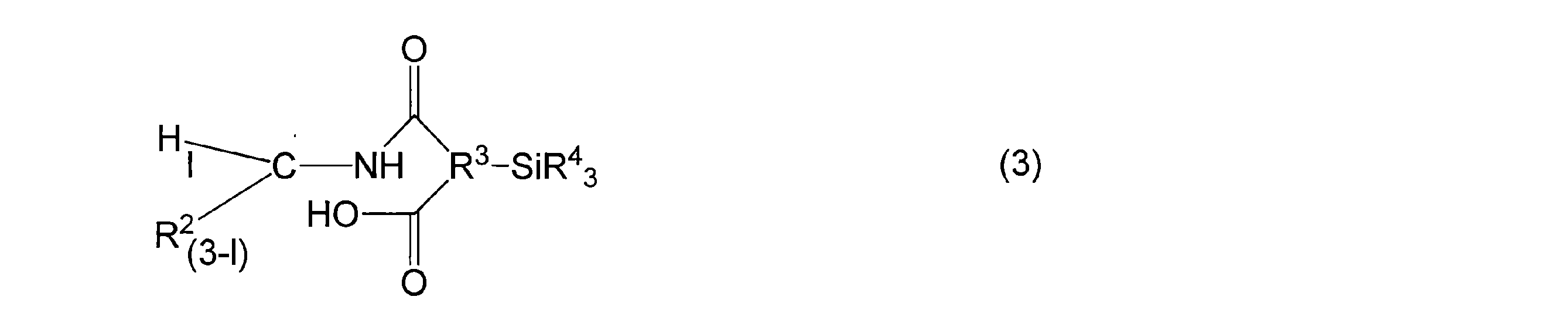
(G)一般式(3)で表されるシランカップリング剤を含有することで、硬化膜の基板への接着性及び後工程で晒されるアルカリ又は酸への耐薬品性がさらに向上する。一般式(3)中のR2としては、メチル基、エチル基又はブチル基が好ましく、原料入手の観点からメチル基又はエチル基がより好ましい。一般式(3)中のR3としては、アルキル基が好ましく、有機溶剤への溶解性の観点から炭素数3~10のアルキル基がより好ましい。

500mLの三口フラスコに47.7g(0.35mol)のメチルトリメトキシシラン(以下、「MTMS」)、99.2g(0.5mol)のフェニルトリメトキシシラン(以下、「PTMS」)、39.4g(0.15mol)の3-トリメトキシシリルプロピルコハク酸(以下、「SuTMS」)及び152.3gのプロピレングリコールメチルエーテルアセテート(以下、「PGMEA」)を仕込み、40℃のオイルバスに漬けて撹拌しながら、56.7gの水に0.372gのリン酸(仕込みモノマーに対して0.2質量%)を溶かしたリン酸水溶液を滴下ロートで10分かけて添加した。40℃で1時間撹拌した後、オイルバス温度を70℃に設定して1時間撹拌し、さらにオイルバスを30分かけて115℃まで昇温した。昇温開始1時間後に溶液の内温が100℃に到達し、そこから2時間加熱撹拌した(内温は100~110℃)。反応中に副生成物であるメタノール及び水を、リービッヒ冷却装置を用いて留去した。得られたポリシロキサンのPGMEA溶液に、ポリマー濃度が40質量%となるようにPGMEAを加えてシロキサン樹脂溶液(B1)を得た。なお、得られたポリマーのMwをGPCにより測定したところ6000(ポリスチレン換算)であった。
表1に示すモノマー比の割合でアルコキシシラン化合物を仕込み、シロキサン樹脂溶液(B2)~(B7)を得た。ポリマー主鎖中のモノマー単位構造をユニットとすると、モノマー比がそのままユニット比となる。

・ AcTMS:アクリロイルオキシプロピルトリメトキシシラン
・ EpTMS:2,3-エポキシシクロヘキシルエチルトリメトキシシラン
・ DMDMS:ジメチルジメトキシシラン
・ DPDMS:ジフェニルジメトキシシラン
・ FTMS:トリフルフルオロプロピルトリメトキシシラン
(合成例8 アクリル樹脂溶液(B8)の合成)
500mLのフラスコに2gの2,2’-アゾビス(イソブチロニトリル)(以下、「AIBN」)及び50gのPGMEAを仕込んだ。その後、26.5g(0.31mol)のメタクリル酸(表中、「MA」)、21.3g(0.21mol)のスチレン(表中、「St」)及び37.7g(0.15mol)のトリシクロ[5.2.1.02,6]デカン-8-イルメタクリレート(以下、「TCDMA」)を仕込み、室温でしばらく撹拌してから、フラスコ内をバブリングによって十分に窒素置換した後、70℃で5時間加熱撹拌した。次に、得られた溶液に14.6g(0.09mol)のメタクリル酸グリシジル(以下、「GMA」)、1gのクロムアセチルアセトナート(以下、「Cr(AcAc)3」)、0.2gのp-メトキシフェノール及び100gのPGMEAを添加し、90℃で4時間加熱撹拌した。反応終了後、固形分濃度が40質量%になるようにPGMEAを加え、アクリル樹脂溶液(B8)を得た(Mw=15000(ポリスチレン換算))。
付加反応に用いる触媒をジメチルベンジルアミンとする以外は合成例1と同様にして、アクリル樹脂溶液(B9)を得た(Mw=15000(ポリスチレン換算))。
AIBNの添加量を1gとする以外は合成例1と同様にして、アクリル樹脂溶液(B10)を得た(Mw=30000(ポリスチレン換算))。
AIBNの添加量を4gとする以外は合成例1と同様にして、アクリル樹脂溶液(B11)を得た(Mw=8000(ポリスチレン換算))。
500mLのフラスコに2gのAIBN及び50gのPGMEAを仕込んだ。その後、23.1g(0.27mol)のメタクリル酸(表中、「MA」)、31.5g(0.18mol)のベンジルメタクリレート(表中、「BzMA」)及び32.8g(0.15mol)のTCDMAを仕込み、室温でしばらく撹拌してから、フラスコ内をバブリングによって十分に窒素置換した後、70℃で5時間加熱撹拌した。次に、得られた溶液に12.7g(0.09mol)のGMA、1gのCr(AcAc)3、0.2gのp-メトキシフェノール及び100gのPGMEAを添加し、90℃で4時間加熱撹拌した。反応終了後、固形分濃度が40質量%になるようにPGMEAを加え、アクリル樹脂溶液(B11)を得た(Mw=15000(ポリスチレン換算))。
500mLのフラスコに2gのAIBN及び50gのPGMEAを仕込んだ。その後、29.4g(0.3mol)のメタクリル酸(表中、「MA」)、26.7g(0.26mol)のスチレン(表中、「St」)及び25.7g(0.26mol)のメタクリル酸メチル(表中、「MMA」)を仕込み、室温でしばらく撹拌してから、フラスコ内をバブリングによって十分に窒素置換した後、70℃で5時間加熱撹拌した。次に、得られた溶液に18.2g(0.13mol)のGMA、1gのCr(AcAc)3、0.2gのp-メトキシフェノール及び100gのPGMEAを添加し、90℃で4時間加熱撹拌した。反応終了後、固形分濃度が40質量%になるようにPGMEAを加え、アクリル樹脂溶液(B13)を得た(Mw=15000(ポリスチレン換算))。
500mLのフラスコに4gのAIBN及び150gのPGMEAを仕込んだ。その後、44.1g(0.51mol)のメタクリル酸(表中、「MA」)及び34.2g(0.85mol)のメタクリル酸メチル(表中、「MMA」)を仕込み、室温でしばらく撹拌してから、フラスコ内をバブリングによって十分に窒素置換した後、70℃で5時間加熱撹拌した。次に、得られた溶液に36.4g(0.26mol)のGMA、2gのCr(AcAc)3、0.2gのp-メトキシフェノール及び100gのPGMEAを添加し、90℃で4時間加熱撹拌した。反応終了後、固形分濃度が40質量%になるようにPGMEAを加え、アクリル樹脂溶液(B14)を得た(Mw=20000(ポリスチレン換算))。
500mLのフラスコに2gのAIBN及び150gのPGMEAを仕込んだ。その後、17.6g(0.21mol)のメタクリル酸(表中、「MA」)、21.3g(0.21mol)のスチレン(表中、「St」)及び37.7g(0.17mol)のTCDMA、23.4g(0.10mol)のグリセロールジメタクリレート(以下、「GCDMA」)を仕込み、室温でしばらく撹拌してから、フラスコ内をバブリングによって十分に窒素置換した後、70℃で5時間加熱撹拌した。反応終了後、固形分濃度が40質量%になるようにPGMEAを加え、アクリル樹脂溶液(B15)を得た(Mw=9000(ポリスチレン換算))。
500mLのフラスコに4gのAIBN及び150gのPGMEAを仕込んだ。その後、16.9g(0.20mol)のメタクリル酸(表中、「MA」)、28.5g(0.27mol)のスチレン(表中、「St」)及び26.8g(0.12mol)のGCDMA、27.8g(0.20mol)のGMAを仕込み、室温でしばらく撹拌してから、フラスコ内をバブリングによって十分に窒素置換した後、70℃で5時間加熱撹拌した。反応終了後、固形分濃度が40質量%になるようにPGMEAを加え、アクリル樹脂溶液(B16)を得た(Mw=9000(ポリスチレン換算))。エポキシ基とカルボン酸の付加触媒を添加していないため、GMAのエポキシ基とMAユニット由来のカルボン酸とは反応せず、GMAユニットが生成する。
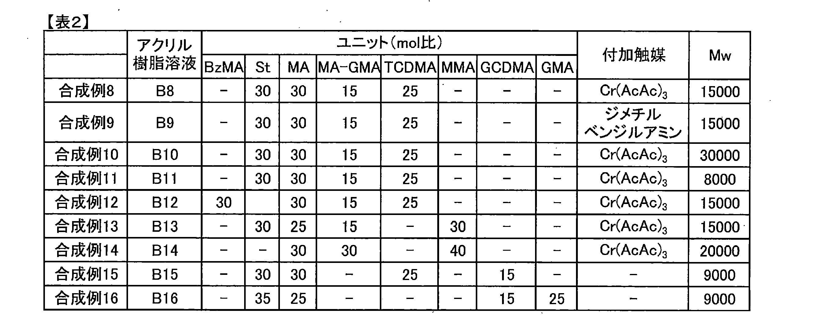
148gの1,1-ビス(4-(2,3-エポキシプロピルオキシ)フェニル)-3-フェニルインダン、47gのアクリル酸、1gのテトラブチルアンモニウムアセテート(以下、TBAA)、2.0gのtert-ブチルカテコール及び244gのPGMEAを仕込み、120℃で5時間撹拌した。室温まで冷却した後、71gのビフェニルテトラカルボン酸二無水物及び1gのTBAAを加えて110℃で3時間撹拌した。室温まで冷却した後、9gのテトラヒドロフタル酸無水物を加えて120℃で5時間撹拌した。反応終了後、500gのPGMEAを加え、付加触媒を除去するために反応溶液を1規定ギ酸水溶液で分液抽出処理し、硫酸マグネシウムで乾燥後、固形分濃度が40質量%になるようにロータリーエバポレーターで濃縮し、ポリエステル樹脂(B17)を得た(Mw=5000)。
PGMEA200gに3-トリメトキシシリルプロピルコハク酸無水物41.97g(160mmol)とt-ブチルアミン11.70g(160mmol)を加えてしばらく室温にて撹拌した後、40℃にて2時間撹拌した。その後80℃まで昇温し、6時間反応させた。得られた溶液を固形分濃度が20質量%になるようにPGMEAで希釈し、3-(tert-ブチルカルバモイル)-6-(トリメトキシシリル)へキサン酸、2-(2-(tert-ブチルアミノ)-2-オキソエチル)-5-(トリメトキシシリル)ペンタン酸の混合溶液(G1)を得た。
21.00gの白色顔料すなわち二酸化チタン顔料(CR-97;石原産業(株)製)、13.13gのシロキサン樹脂溶液(B1)及び0.87gのPGMEAを混合した後、ジルコニアビーズが充填されたミル型分散機を用いて分散し、顔料分散液(MW-1)を得た。得られたミルベースについてレーザー回折法によりメディアン径を測定したところ、260nmであった。
表3、表4、表5及び表6に示す比率で、調製例1と同様にしてネガ型感光性白色組成物を調製した。

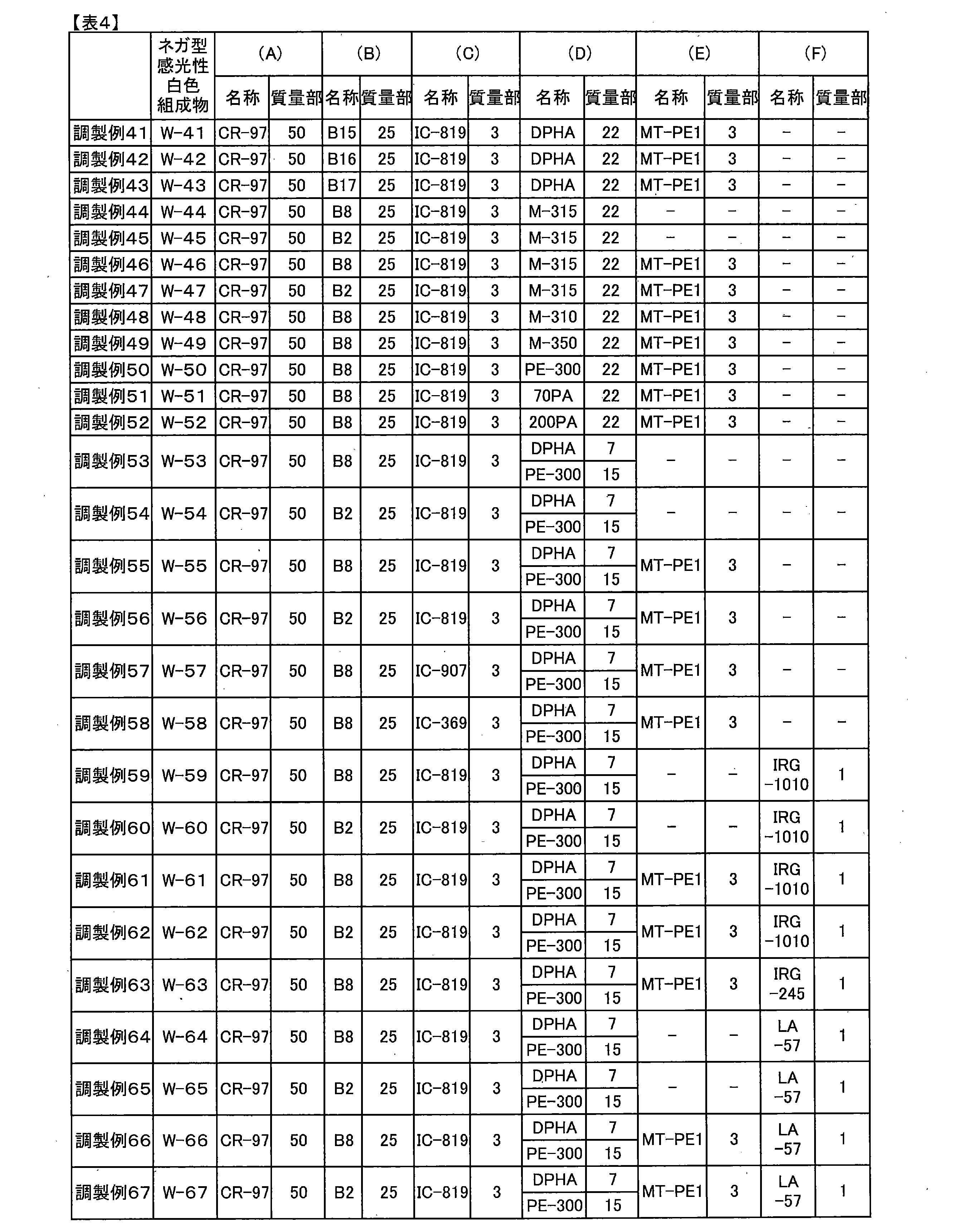
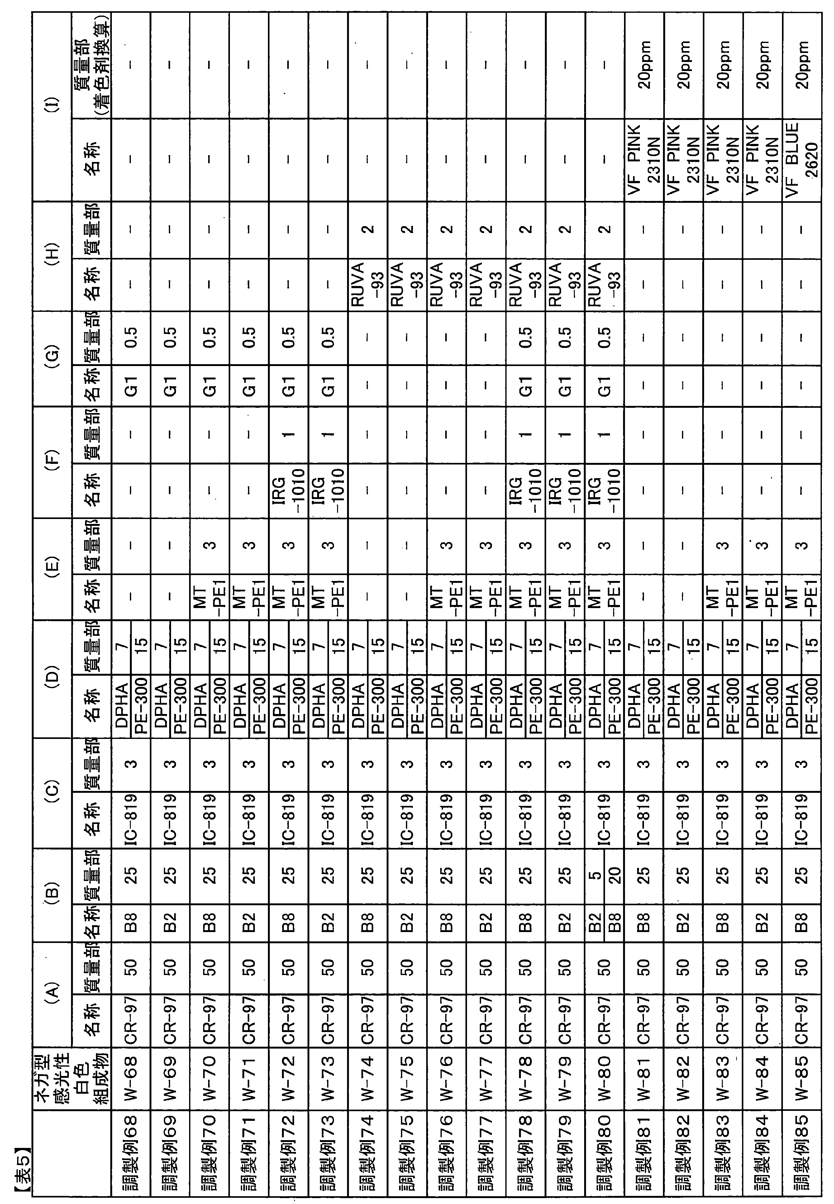
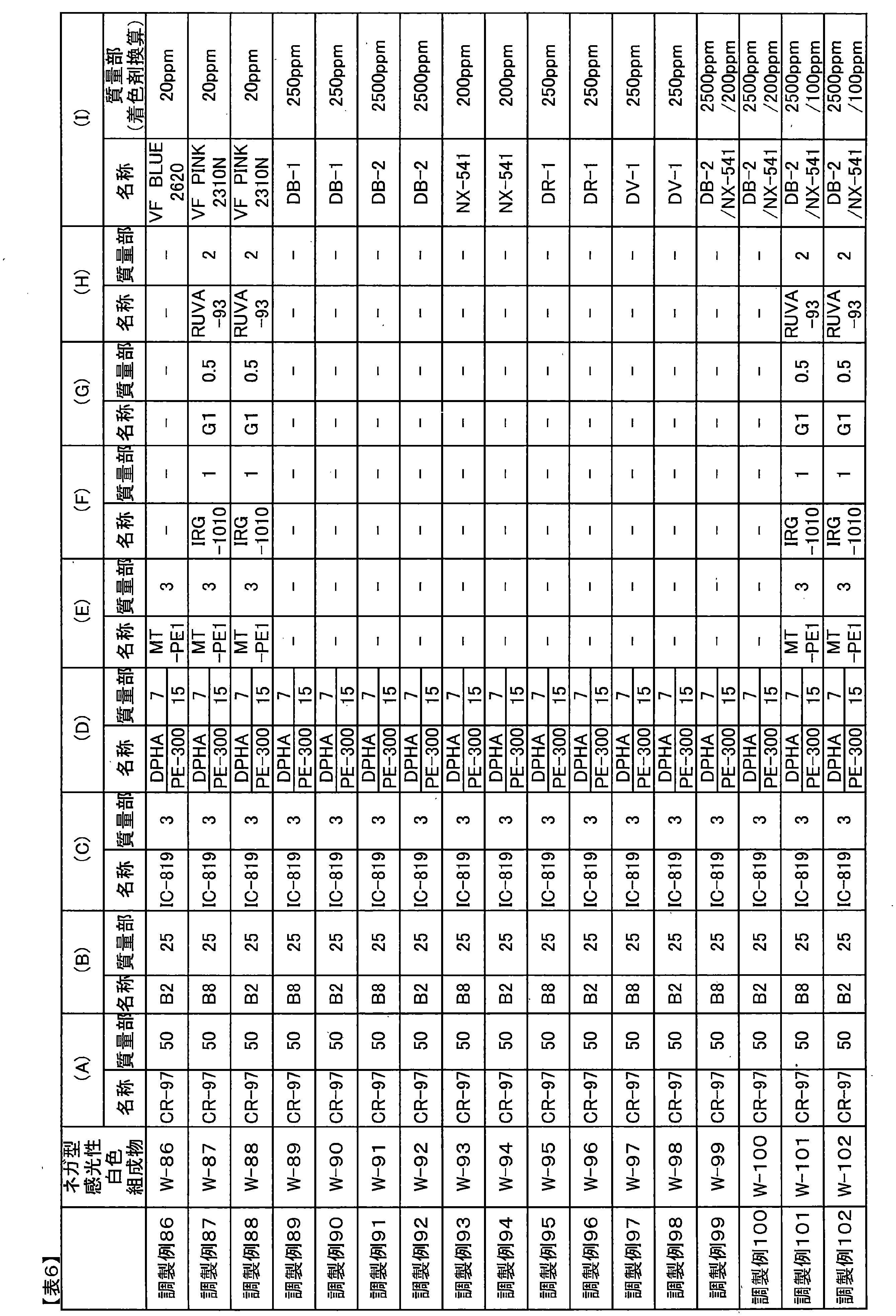
・ CR-97:二酸化チタン顔料(アルミナ/ジルコニア被覆、石原産業(株)製)
・ JR-605:二酸化チタン顔料(アルミナ被覆、テイカ工業(株)製)
・ R960:二酸化チタン顔料(アルミナ/シリカ被覆、デュポン(株)製)
・ MT-PE1:ペンタエリスリトールテトラキス(3-メルカプトブチレート)(昭和電工(株)製)
・ MT-BD1:1,4-ブチレングリコール(3-メルカプトブチレート)(昭和電工(株)製)
・ MT-NR1:トリス(3-メルカプトブチリルオキシエチル)イソシアヌレート(昭和電工(株)製)
・ TPMB:トリメチロールプロパントリス(3-メルカプトブチレート)(昭和電工(株)製)
・ TEMB:トリメチロールエタントリス(3-メルカプトブチレート)(昭和電工(株)製)
・ PEMP:ペンタエリスリトールテトラキス(3-メルカプトプロピオネート)
・ M-315:イソシアヌル酸-EO変性トリ及びジアクリレート(平均EO数=3)混合物(東亞合成(株)製)
・ M-310:トリメチロールプロパン-PO変性トリアクリレート(平均PO数=3)(東亞合成(株)製)
・ M-350:トリメチロールプロパン-EO変性トリアクリレート(平均EO数=3)(東亞合成(株)製)
・ 200PA:トリプロピレングリコールジグリシジルエーテルアクリレート(共栄社化学(株)製)
・ 70PA:プロピレングリコールジグリシジルエーテルアクリレート(共栄社化学(株)製)
・ PE-300:ポリエチレングリコール300-ジアクリレート(第一工業製薬(株)製)
・ IRG-1010:ペンタエリスリトールテトラキス[3-(3,5-ジ-tert-ブチル-4-ヒドロキシフェニル)プロピオネート(BASFジャパン(株)製)
・ IRG-245:エチレンビス(オキシエチレン)ビス(3-(5-t-ブチル-4-ヒドロキシ-m-トリル)プロピオネート(BASFジャパン(株)製)
・ LA-57:テトラキス(2,2,6,6-テトラメチル-4-ピリジル)ブタン-1,2,3,4-テトラカルボキシレート(アデカ(株)製)
・ IC-907:2-メチル-1-(4-メチルチオフェニル)-2-モルフォリノプロパン-1-オン(BASFジャパン(株)製)
・ IC-369:2-ベンジル-2-ジメチルアミノ-1-(4-モルフォリノフェニル)-ブタノン-1(BASFジャパン(株)製)
・ RUVA-93:2-(2’-ヒドロキシ-5’-メタクリロキシエチルフェニル)-2H-ベンゾトリアゾール(大塚化学(株)製)
・ VF BLUE 2620:C.I. Solvent BLUE 44 (オリエント化学(株)製、VF=VALIFAST)
・ VF PINK 2310N:C.I. Solvent RED 218 (オリエント化学(株)製、VF=VALIFAST)
・ NX-541:PR101(酸化鉄)分散液(大日精化製)(固形分濃度80質量%、着色材/樹脂(質量比)=2/1)
(調製例103 非感光性白色組成物(HW-1)の調製)
45gのCR-97及び10gのアクリル樹脂溶液(B7)の混合物を三本ローラーを用いて混練し、非感光性白色組成物(HW-1)を得た。
45gのCR-97及び10gのシリコーン系樹脂「840 RESIN(東レダウコーニング(株)製)」の混合物を三本ローラーを用いて混練し、非感光性白色組成物(HW-2)を得た。
50gのアクリル溶液(B1)、16gのジペンタエリトリトールペンタアクリレート(日本化薬(株)製)、2gの1.2-オクタンジオン,1-[4-(フェニルチオ)-,2-(O-ベンゾイルオキシム)](“IRGACURE”(登録商標)OXE-01;BASF製)、31.9gのダイアセトンアルコール及び0.1gのポリエーテル変性ポリジメチルシロキサン(BYK-333;ビックケミー製)を混合し、ネガ型感光性透明組成物(Cr-1)を調製した。
黒色顔料(BASF社製“Irgaphor Black S0100CF”)を120g、アクリルポリマー溶液(B12)を98g、高分子分散剤としてディスパービックLPN-21116(DP-1;ビックケミー社製;PMA40質量%溶液)を100g及びPMA682gをタンクに仕込み、ホモミキサー(プライミクス製)で20分撹拌し、予備分散液を得た。その後、0.05mmφジルコニアビーズ(YTZボール;ネツレン製)を75%充填した遠心分離セパレーターを具備したウルトラアペックスミル(寿工業製)に予備分散液を供給し、回転速度8m/sで3時間分散を行い、固形分濃度20質量%、着色材/樹脂(質量比)=60/40の黒色材分散液DBk-1を得た。
着色材として黒色顔料Irgaphor Black S0100CFの代わりに紫色有機顔料PV23(クラリアント製)を用いた以外は、黒色材分散液DBk-1と同様にして、紫色材分散液DV-1を得た。
着色材として黒色顔料Irgaphor Black S0100CFの代わりに青色有機顔料PB15:6(東洋インキ(株)製)を用いた以外は、黒色材分散液DBk-1と同様にして、青色材分散液DB-1を得た。
着色材として黒色顔料Irgaphor Black S0100CFの代わりに青色無機顔料PB28(大日精化工業(株)製)を用いた以外は、黒色材分散液DBk-1と同様にして、青色材分散液DB-2を得た。
着色材として黒色顔料Irgaphor Black S0100CFの代わりに赤色有機顔料PR177(BASF製)を用いた以外は、黒色材分散液DBk-1と同様にして、赤色材分散液DR-1を得た。
31.52gのPGMEAに、光重合開始剤として0.5gのOXE-01を添加し、固形分が溶解するまで撹拌した。
黒色材分散液DBk-1の代わりに紫色材分散液DV-1を用いた以外は、ネガ型感光性黒色組成物(Bk-1)の調製と同様にして、ネガ型感光性着色組成物(V-1)を得た。
ネガ型感光性透明組成物(Cr-1)に、顔料濃度が固形分に対して0.1質量部となるように紫色材分散液DV-1を加えて、ネガ型感光性着色組成物(V-2)を得た。
上記の調製例1で得られたネガ型感光性白色組成物(W-1)について、下記(i)~(vi)の方法で物性の評価を実施し、下記(vii)の方法でタッチパネルの製造に関する評価を実施した。
10cm角のアルカリガラス基板(日本板硝子製、厚さ=0.5mm)上に、ネガ型感光性白色組成物(W-1)を任意の回転数でスピンコートし、基板をホットプレート(SCW-636;大日本スクリーン製造(株)製)を用いて100℃で3分間プリベークし、膜厚15μmの硬化膜を形成した。次に、PLA(PLA-501F;キヤノン(株)製)を用いて超高圧水銀灯を光源とし、150μm幅のライン&スペースパターンを有したマスクを介して、露光量200mJ(i線)、マスクギャップ150μmで露光した。その後、自動現像装置(滝沢産業(株)製;AD-2000)を用いて、2.38質量%TMAH水溶液(ELM-D;三菱ガス化学(株)製)又は0.045質量%KOH水溶液で60秒間シャワー現像し、次いで水で30秒間リンスした。現像後のパターンを、抜け性及び現像接着性の二項目について、以下の判断基準に基づいて評価を行った。
・抜け性
S:直線形状の線幅100μmの抜きパターンに残渣がない。
A:直線形状の線幅100μmの抜きパターンに残渣があるが、線幅150μmの抜きパターンに残渣がない。
B:直線形状の線幅150μmの抜きパターンに残渣があるが、線幅200μmの抜きパターンに残渣がない。
C:直線形状の線幅200μmの抜きパターンに残渣がある。
・現像接着性
S:50μm幅以上のラインアンドスペースパターン(=L/S)の露光部が、基板から剥がれなく残存している。
A:100μm幅以上のL/Sの露光部が基板から剥がれなく残存しているが、100μm幅以下のL/Sは剥がれている
B:150μm幅以上のL/Sの露光部が基板から剥がれなく残存しているが、150μm幅以下のL/Sは剥がれている。
C:150μm幅以上のL/Sの露光部が基板から剥がれている。
ただし、現像接着性の評価は抜け性が「S、A、B」の場合に実施した。
上記(i)と同様にして、150μm幅のL/Sをパターン加工後、基板をオーブン(IHPS-222;エスペック(株)製)を用いて空気中230℃で30分間キュアして、硬化膜を形成した。得られた硬化膜の断面を切り出し、走査型電子顕微鏡を用いて観察して、以下の判断基準に基づいてパターン形状を評価した。また、得られた硬化膜の膜厚を触針型段差計で測定したところ、15μmであった。
A:テーパー角60°未満
B:テーパー角60°以上
C:アンダーカット形状
(iii)接着性の評価
10cm角のアルカリガラス基板上に、ネガ型感光性白色組成物をキュア後の膜厚が15μmとなるようにスピンコーターにてそれぞれ塗布し、基板をホットプレートを用いて100℃で3分間プリベークし、膜厚15μmの塗膜を形成した。次に、PLAを用いて超高圧水銀灯を光源とし、基板全面に露光した。その後、自動現像装置を用いて、2.38質量%TMAH水溶液又は0.045質量%KOH水溶液で120秒間シャワー現像し、次いで水で30秒間リンスした。オーブンを用いて空気中230℃で30分間キュアして、硬化膜を形成した。
5:剥離面積=0%
4:剥離面積=<5%
3:剥離面積=5~14%
2:剥離面積=15~34%
1:剥離面積=35%~64%
0:剥離面積=65%~100%
(iv)耐薬品性の評価
上記(iii)と同様にして硬化膜を形成したガラス基板を二枚作製し、一枚について調製例50で得られたネガ型感光性透明組成物(Cr-1)をキュア後の膜厚が2μmとなるように、スピンコーターにて塗布し、基板をホットプレートを用いて100℃で2分間プリベークし、膜厚2μmの硬化膜を作製した。次に、PLAを用いて超高圧水銀灯を光源とし、露光量100mJ(i線)、で全面露光した。その後、自動現像装置を用いて、2.38質量%TMAHで60秒間シャワー現像し、次いで水で30秒間リンスした。最後に、オーブンを用いて空気中230℃で30分間キュアして、白色硬化膜上に透明保護膜を形成した。
(1) ITOエッチャント(36質量%塩化水素水溶液/60質量%硝酸水溶液/水=4/1/5(質量比)混合溶液)(35℃、2分)
(2) 4質量%水酸化ナトリウム水溶液(40℃、2分)
(3) ナガセケムテック(株)製「N-300」(60℃、3分)
以下の判断基準に基づいて耐薬品性を評価した。
以下の基準の評価を実施した。
S:白色硬化膜単独での薬品処理後の接着性評価が4~5。
A:白色硬化膜単独での薬品処理後の接着性評価が1~3であり、白色硬化膜+透明保護膜での薬品処理後の接着性評価が4~5。
B:白色硬化膜単独での薬品処理後の接着性評価が0であり、白色硬化膜+透明保護膜での薬品処理後の接着性評価が1~3。
C:白色硬化膜単独での薬品処理中に硬化膜が剥離する。
上記(iii)と同様にして硬化膜を形成したガラス基板を作製し、X-rite 361T(visual)densitometerを用いて入射光及び透過光それぞれの強度を測定し、以下の式(1)よりOD値を算出した。
OD値 = log10(I0/I) ・・・ 式(1)
I0:入射光強度
I:透過光強度
(vi)色特性の評価
上記(iii)と同様にして硬化膜を形成したガラス基板を二枚作製し、一枚をさらにオーブンを用いて空気中240℃で120分間追加加熱した。それぞれの基板について分分光光度計(UV-2450;株式会社島津製作所製)を用いて、ガラス基板側からの全反射光の反射率を測定し、CIE1976(L*,a*,b*)色空間にて表示した。それら値を用いて、以下の式(2)より追加加熱前後の色差(以下、「ΔEab」)を算出した。
ΔEab=(X1^2+X2^2+X3^2)^0.5 ・・・ 式(2)
ここで、
X1 : {L*(0)}-{L*(1)}
X2 : {a*(0)}-{a*(1)}
X3 : {b*(0)}-{b*(1)}
であり、L*(0)、a*(0)、b*(0)は、それぞれ、膜特性評価用の硬化膜のL*,a*,b*の値を示し、L*(1)、a*(1)、b*(1)は、それぞれ、追加熱処理した硬化膜のL*,a*,b*の値を示す。
以下の手順により、タッチパネル基板を作製した。
10cm×10cm、厚み0.7mmの強化ガラス上に、調製例1で得られたネガ型感光性白色組成物(W-1)をキュア後の膜厚が15μmとなるようにスピンコートし、基板をホットプレートを用いて100℃で3分間プリベークした。次に、PLAを用いて超高圧水銀灯を光源とし、タッチパネル用の遮光パターン(線幅=3000μm)を有したマスクを介して、露光量200mJ(i線)、マスクギャップ150μmで露光した。その後、自動現像装置を用いて、2.38質量%TMAH水溶液で120秒間シャワー現像し、次いで水で30秒間リンスした。最後に基板をオーブンを用いて空気中230℃で30分間キュアして、白色遮光パターンを有するガラス基板を作製した(図1のaに相当)。
上記(1)で得られたガラス基板にスパッタリング装置HSR-521A((株)島津製作所製)を用いて、RFパワー1.4kW、真空度6.65×10⁻¹Paで12.5分間スパッタリングすることにより、膜厚が150nmのITOを成膜し、ポジ型フォトレジスト(OFPR-800;東京応化工業(株)製)を塗布し、80℃で20分間プリベークして膜厚1.1μmのレジスト膜を得た。PLAを用いて、得られた膜に超高圧水銀灯をマスクを介してパターン露光した後、自動現像装置を用いて2.38質量%TMAH水溶液で90秒間シャワー現像し、次いで水で30秒間リンスした。その後、3.5質量%シュウ酸水溶液に150秒浸すことでITOをエッチングし、50℃の剥離液(4%水酸化カリウム水溶液)で120秒処理することでフォトレジストを除去し、230℃で30分アニール処理を加え、膜厚150nmのパターン加工されたITO(図1の符号3)を有するガラス基板を作製した(図1のbに相当)。
上記(2)で得られたガラス基板上に調製例50で得られたネガ型感光性透明組成物(Cr-1)を用いて、膜厚を2μmとし、パターンマスクを介して露光を行う以外は(1)と同様にして、透明絶縁膜(図1の符号4)を作製した(図1のcに相当)。
上記(3)で得られたガラス基板上に、ターゲットとしてモリブデン及びアルミニウムを用いて、エッチング液としてH3PO4/HNO3/CH3COOH/H2O=65/3/5/27(質量比)混合溶液を用いた以外は(1)と同様にして、膜厚250nmのMAM配線(図1の符号5)を作製し(図1のdに相当)、タッチパネル基板を完成させた(図1のd、図2)。
(viii)粘度の測定
調製直後及び40℃/1週間放置後の白色組成物について、E型粘度計(東機産業(株)製「VISCOMETER TV-25」)を用いて25℃での粘度を測定した。
(ix)クラック耐性の評価
10cm角の無アルカリガラス基板上に、ネガ型感光性着色組成物をキュア後の膜厚が10μm、15μm、20μm、及び25μmとなるようにスピンコーター(1H-360S;ミカサ(株)製)にてそれぞれ塗布し、基板をホットプレートを用いて100℃で2分間プリベークし、硬化膜を形成した。次に、PLAを用いて超高圧水銀灯を光源とし、露光量200mJ(i線)で全面露光した。その後、自動現像装置を用いて、2.38質量%水酸化テトラメチルアンモニウム水溶液で60秒間シャワー現像し、次いで水で30秒間リンスした。最後に、オーブン(IHPS-222;エスペック(株)製)を用いて空気中230℃で1時間キュアして、硬化膜を形成した。得られた硬化膜のクラックの発生有無を目視にて確認し1つでもクラックがあれば、その膜厚でのクラック耐性はないと判断した。例えば、膜厚15μmではクラックがなく、膜厚20μmではクラックがあった場合には、耐クラック膜厚を「>15μm」と判定した。また、20μmでもクラックがない場合の耐クラック膜厚を「>20μm」、5μmでもクラックがある場合の耐クラック膜厚を「<5μm」と、それぞれ判定した。
調製例2~102で得られたネガ型感光性白色組成物を用いて、実施例1と同様にして(i)~(ix)の評価を実施した。評価結果を、表7、表8、表9、表10、表11及び表12に示す。
10cm角のアルカリガラス基板(日本板硝子製、厚さ=0.5mm)上に、ネガ型感光性白色組成物(W-29)を任意の回転数でスピンコートし、膜厚10μmの塗膜を形成した。次に、PLAを用いて超高圧水銀灯を光源とし、190μm幅のライン&スペースパターンを有したマスクを介して、露光量150mJ(i線)、マスクギャップ150μmで露光した。その後、自動現像装置を用いて、2.38質量%TMAH水溶液で120秒間シャワー現像し、次いで水で30秒間リンスした。オーブンを用いて空気中230℃で30分間キュアして、硬化膜を形成した。得られた硬化膜を具備する基板に、膜厚5μmとなるように塗布し、150μm幅のライン&スペースパターンを有したマスクを介して露光する以外は(1層目とアライメントをパターンセンターが一致するようにアライメントを実施)同様にして、2層目の硬化膜を形成した。得られたパターンを、抜け性及び現像接着性の二項目について、評価を行った。その他の評価は上記(ii)~(vi)の項目について、同様に2層に加工した上で実施した。
ネガ型感光性白色組成物(W-29)の代わりにネガ型感光性白色組成物(W-56)を用いる以外は実施例103と同様に実施した。
1層目の膜厚及び線幅と2層目の膜厚及び線幅を入れ替えて加工する以外は実施例103と同様に実施した。
ネガ型感光性白色組成物(W-29)の代わりにネガ型感光性白色組成物(W-56)を用いる以外は実施例105と同様に実施した。
調製例103で得られた非感光性白色組成物(HW-1)について、スクリーン印刷機を用いて、キュア後の膜厚が15μmとなるようにスキージと垂直方向に直線形状の線幅200μmの抜きパターンの形成を試みた。しかしながら抜きパターンが埋もれてしまい、パターン形成には至らなかった。
調製例104で得られた非感光性白色組成物(HW-2)について、スクリーン印刷機を用いて、キュア後の膜厚が15μmとなるようにスキージと垂直方向に直線形状の線幅200μmの抜きパターンの形成を試みた。しかしながら抜きパターンが埋もれてしまい、パターン形成には至らなかった。

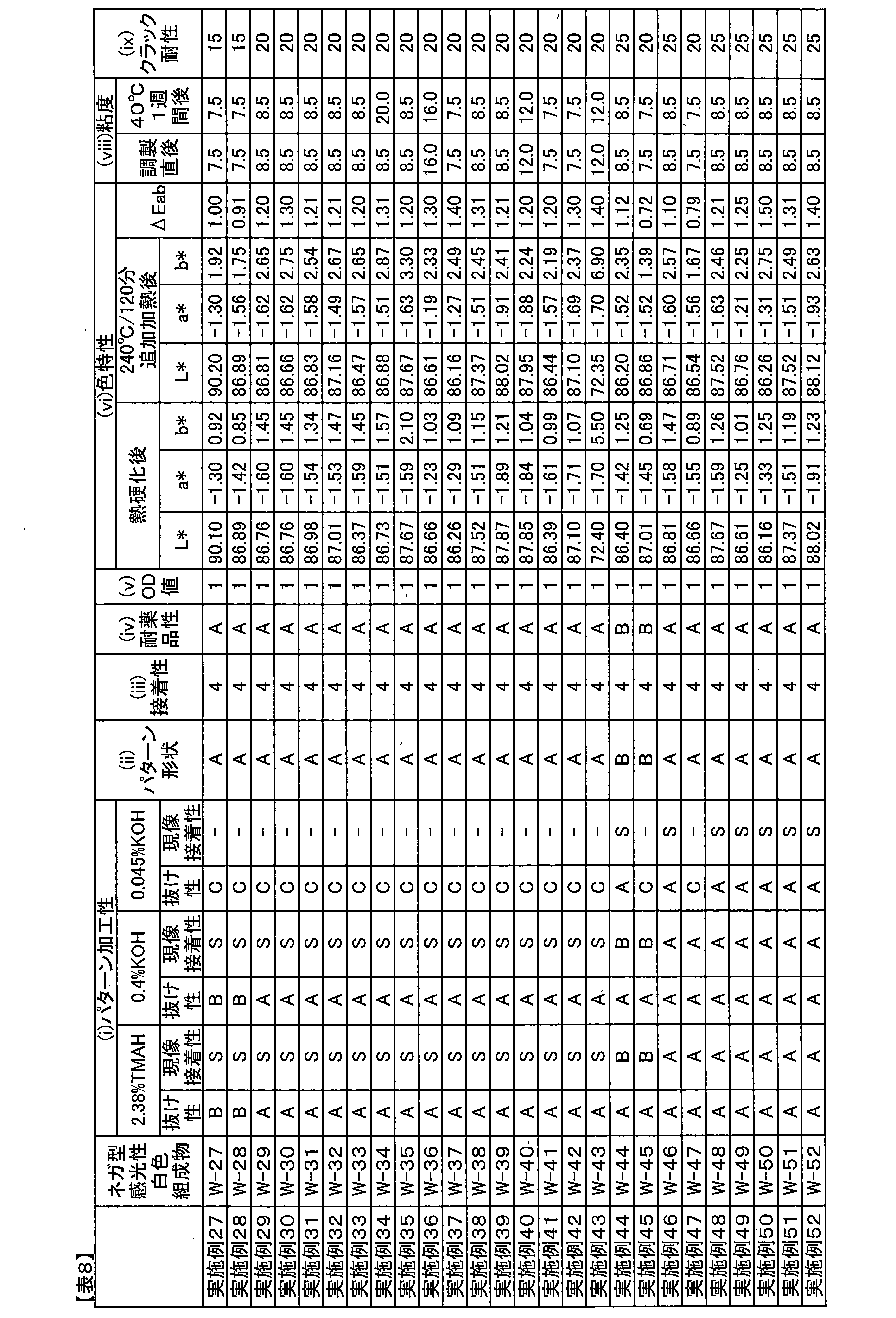

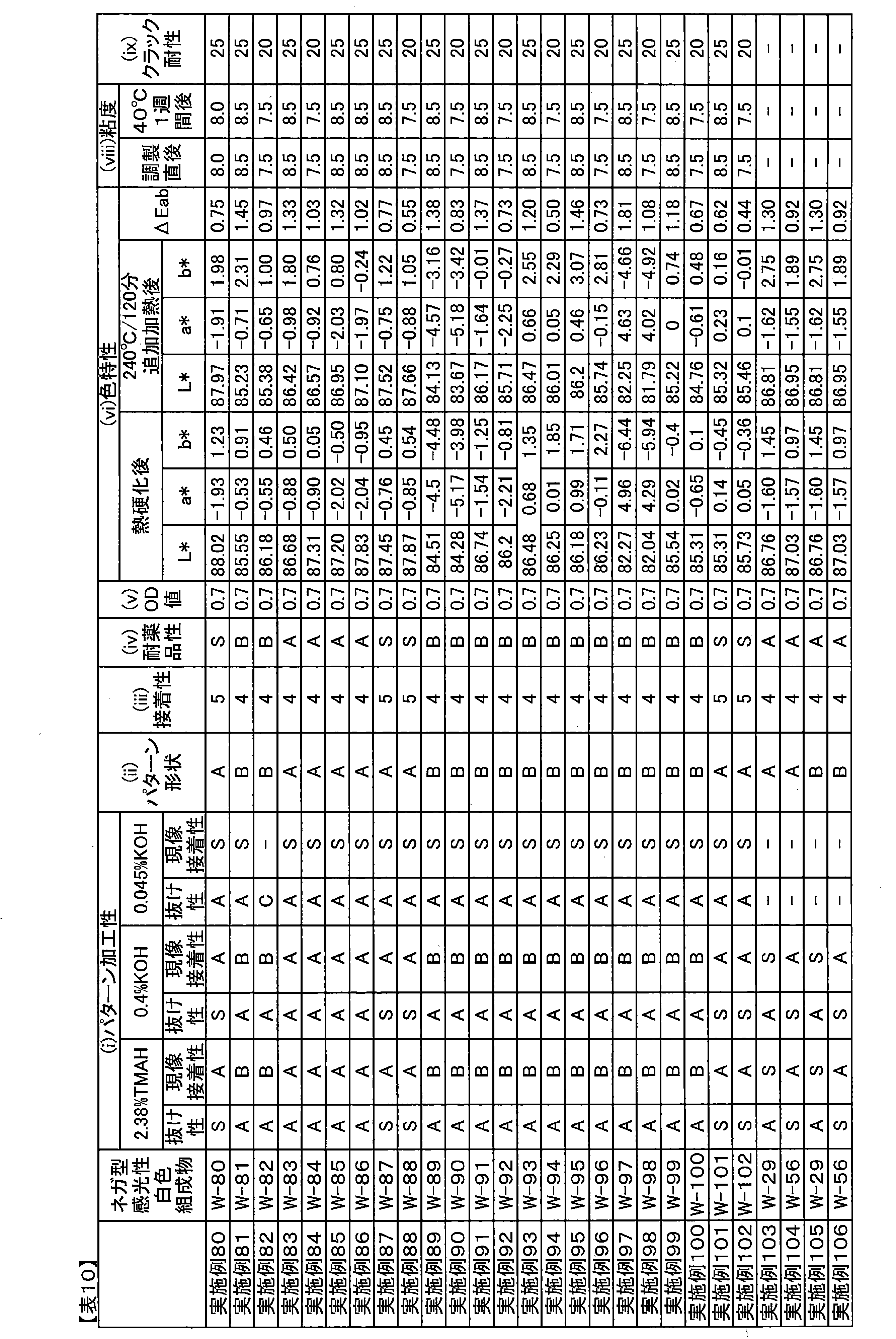
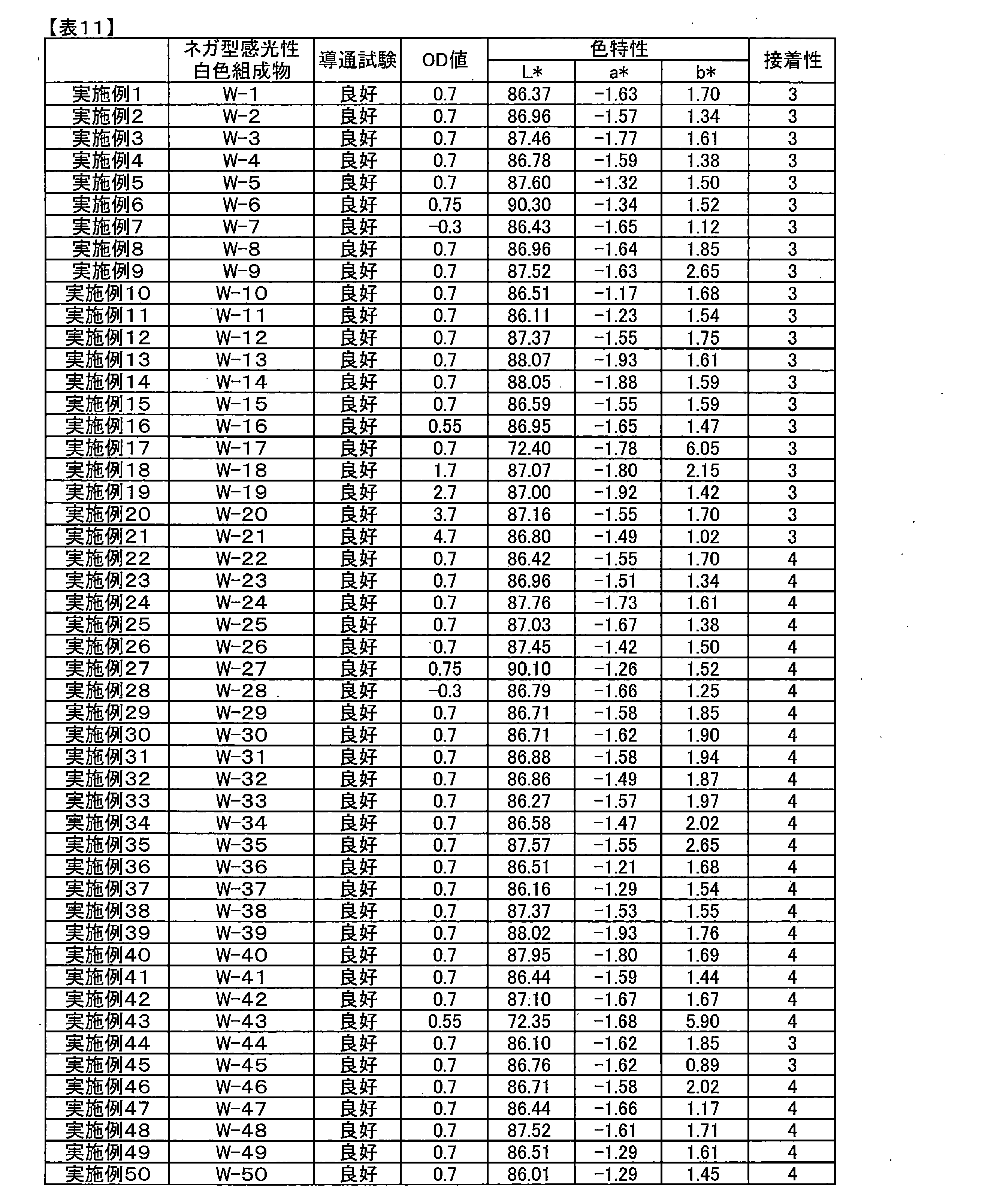
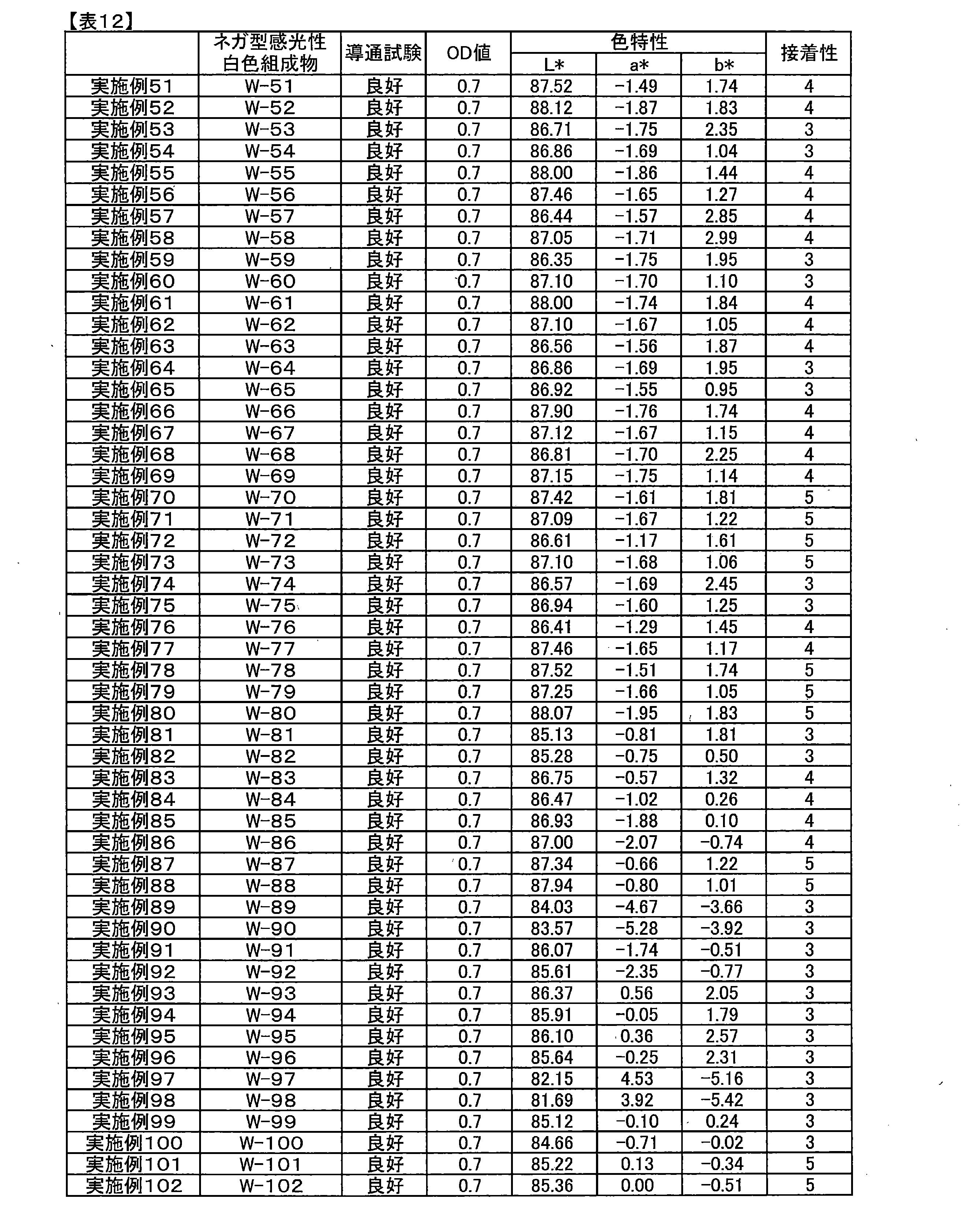
以下の手順により、タッチパネル基板を作製した。
調製例29で得られたネガ型感光性白色組成物(W-29)を用いて、上記(vii)(1)と同様にして、白色遮光パターンを有するガラス基板を作製した。
上記(1)で得られたガラス基板上に調製例50で得たネガ型感光性透明組成物(Cr-1)を用いて、膜厚を2μmとし、白色遮光パターンより400μm大きいパターンマスクを介して露光を行う以外は上記(vii)(3)と同様にして、透明樹脂膜を有するガラス基板を作製した。
上記(2)で得られたガラス基板に、上記(vii)(2)と同様にして、膜厚150nmのパターン加工されたITOを有するガラス基板を作製した。
上記(3)で得られたガラス基板上に、上記(vii)(3)と同様にして、透明絶縁膜を有するガラス基板を作製した。
上記(4)で得られたガラス基板上に、上記(vii)(4)と同様にして、MAM配線を作製し、タッチパネル基板を完成させた(図3)。
ネガ型感光性白色組成物(W-29)の代わりにネガ型感光性白色組成物(W-56)を用いる以外は実施例107と同様に実施した。
(2)透明樹脂膜の作製の工程において、マスクを介さずに露光する以外は、実施例58と同様にして、タッチパネル基板を完成させた(図4)。
ネガ型感光性白色組成物(W-29)の代わりにネガ型感光性白色組成物(W-56)を用いる以外は実施例107と同様に実施した。
(2)透明樹脂膜の作製の工程の代わりに、高速プラズマCVD成膜装置(PD-270STL;サムコ(株)製)を用い、テトラエトキシシランを原料として、膜厚0.3μmの酸化ケイ素薄膜を形成したこと以外は実施例109と同様に実施した。
ネガ型感光性白色組成物(W-29)の代わりにネガ型感光性白色組成物(W-56)を用いる以外は実施例111と同様に実施した。
(1)白色遮光パターンの作製
調製例29で作製したネガ型感光性白色組成物(W-29)を用いて、上記(vii)(1)と同様にして、白色遮光パターンを有するガラス基板を作製した。
(1)で得られたガラス基板上に、調製例51で得られたネガ型感光性黒色組成物(Bk-1)を用いて、膜厚を2μmとし、白色遮光パターンより400μm小さいパターンマスクを介して露光を行い、現像液を0.045質量%KOH水溶液とする以外は上記(vii)(1)と同様にして、黒色遮光性硬化膜を作製した。
上記(2)で得られたガラス基板に、上記(vii)(2)と同様にして、膜厚150nmのパターン加工されたITOを有するガラス基板を作製した。
上記(3)で得られたガラス基板上に、上記(vii)(3)と同様にして、透明絶縁膜を有するガラス基板を作製した。
上記(4)で得られたガラス基板上に、上記(vii)(4)と同様にして、MAM配線を作製し、タッチパネル基板を完成させた(図5)。
ネガ型感光性白色組成物(W-29)の代わりにネガ型感光性白色組成物(W-56)を用いる以外は実施例113と同様に実施した。
(1)白色遮光パターンの作製
調製例29で得られたネガ型感光性白色組成物(W-29)を用いて、上記(vii)(1)と同様にして、白色遮光パターンを有するガラス基板を作製した。
上記(1)で得られたガラス基板上に、調製例51で得られたネガ型感光性黒色組成物(Bk-1)を用いて、膜厚を2μmとし、白色遮光パターンより400μm小さいパターンマスクを介して露光を行い、現像液を0.045質量%KOH水溶液とする以外は上記(vii)(1)と同様にして、黒色遮光性硬化膜を作製した。
上記(2)で得られたガラス基板上に調製例50で得られたネガ型感光性透明組成物(Cr-1)を用いて、膜厚を2μmとし、白色遮光パターンより400μm大きいパターンマスクを介して露光を行う以外は上記(vii)(3)と同様にして、透明樹脂膜を有するガラス基板を作製した。
上記(3)で得られたガラス基板に、上記(vii)(2)と同様にして、膜厚150nmのパターン加工されたITOを有するガラス基板を作製した。
上記(4)で得られたガラス基板上に、上記(vii)(3)と同様にして、透明絶縁膜を有するガラス基板を作製した。
上記(5)で得られたガラス基板上に、上記(vii)(4)と同様にして、MAM配線を作製し、タッチパネル基板を完成させた(図6)。
ネガ型感光性白色組成物(W-29)の代わりにネガ型感光性白色組成物(W-56)を用いる以外は実施例115と同様に実施した。
(3)透明樹脂膜の作製の工程において、マスクを介さずに露光する以外は、実施例115と同様にして、タッチパネル基板を完成させた(図7)。
ネガ型感光性白色組成物(W-29)の代わりにネガ型感光性白色組成物(W-56)を用いる以外は実施例117と同様に実施した。
(3)透明樹脂膜の作製の工程の代わりに、高速プラズマCVD成膜装置(PD-270STL;サムコ(株)製)を用い、テトラエトキシシランを原料として、膜厚0.3μmの酸化ケイ素薄膜を形成したこと以外は実施例117と同様に実施した。
ネガ型感光性白色組成物(W-29)の代わりにネガ型感光性白色組成物(W-56)を用いる以外は実施例119と同様に実施した。
(2)黒色遮光性硬化膜の作製の工程と、(3)透明樹脂膜の作製の工程との順番を入れ替える以外は、実施例61と同様にして、タッチパネル基板を完成させた(図8)。
ネガ型感光性白色組成物(W-29)の代わりにネガ型感光性白色組成物(W-56)を用いる以外は実施例121と同様に実施した。
(2)黒色遮光性硬化膜の作製の工程と、(3)透明樹脂膜の作製の工程との順番を入れ替える以外は、実施例62と同様にして、タッチパネル基板を完成させた(図9)。
ネガ型感光性白色組成物(W-29)の代わりにネガ型感光性白色組成物(W-56)を用いる以外は実施例123と同様に実施した。
(1)白色遮光パターンの作製
調製例29で得られたネガ型感光性白色組成物(W-29)を用い、上記(vii)と同様にして、白色遮光パターンを有するガラス基板を作製した。
上記(1)で得られたガラス基板上に調製例50で得られたネガ型感光性透明組成物(Cr-1)を用い、膜厚を2μmとし、マスクを介さず露光を行う以外は上記(vii)と同様の手順に従い、透明樹脂膜を有するガラス基板を作製した。
上記(2)で得られたガラス基板上に、調製例51で得られたネガ型感光性黒色組成物(Bk-1)を用い、膜厚を2μmとし、白色遮光パターンより400μm小さいパターンマスクを介して露光を行い、現像液を0.045%KOH水溶液とする以外は上記(vii)と同様の手順に従い、黒色遮光性硬化膜を作製した。
上記(3)で得られたガラス基板上に調製例50で得られたネガ型感光性透明組成物(Cr-1)を用い、膜厚を2μmとし、白色遮光パターンより400μm大きいパターンマスクを介して露光を行う以外は上記(vii)と同様の手順に従い、透明樹脂膜を有するガラス基板を作製した。
上記(4)で得られたガラス基板に、上記(vii)と同様にして、膜厚150nmのパターン加工されたITOを有するガラス基板を作製した。
上記(5)で得られたガラス基板上に、上記(vii)と同様にして、透明絶縁膜を有するガラス基板を作製した。
上記(6)で得られたガラス基板上に、上記(vii)と同様にして、MAM配線を作製し、タッチパネル基板を完成させた(図10)。
ネガ型感光性白色組成物(W-29)の代わりにネガ型感光性白色組成物(W-56)を用いる以外は実施例125と同様に実施した。
(1)白色遮光パターン-1の作製
膜厚=10μm、線幅=2600μmとなるように、調製例29で得られたネガ型感光性白色組成物(W-29)を用い、上記(vii)と同様にして、白色遮光パターンを有するガラス基板を作製した。
上記(1)で得られたガラス基板上に、膜厚=5μm、線幅=3000μmとなるように、調製例29で得られたネガ型感光性白色組成物(W-29)を用い、上記(vii)と同様にして、白色遮光パターンを有するガラス基板を作製した。
上記(2)で得られたガラス基板上に、調製例51で得られたネガ型感光性黒色組成物(Bk-1)を用いて、膜厚を2μmとし、白色遮光パターンより400μm小さいパターンマスクを介して露光を行い、現像液を0.045質量%KOH水溶液とする以外は上記(vii)(1)と同様にして、黒色遮光性硬化膜を作製した。
上記(3)で得られたガラス基板上に調製例50で得られたネガ型感光性透明組成物(Cr-1)を用いて、膜厚を2μmとし、白色遮光パターンより400μm大きいパターンマスクを介して露光を行う以外は上記(vii)(3)と同様にして、透明樹脂膜を有するガラス基板を作製した。
上記(4)で得られたガラス基板に、上記(vii)(2)と同様にして、膜厚150nmのパターン加工されたITOを有するガラス基板を作製した。
上記(5)で得られたガラス基板上に、上記(vii)(3)と同様にして、透明絶縁膜を有するガラス基板を作製した。
上記(6)で得られたガラス基板上に、上記(vii)(4)と同様にして、MAM配線を作製し、タッチパネル基板を完成させた(図11)。
ネガ型感光性白色組成物(W-29)の代わりにネガ型感光性白色組成物(W-56)を用いる以外は実施例127と同様に実施した。
白色遮光パターン-1の作製において、ネガ型感光性白色組成物(W-29)の代わりに調製例104で得られた非感光性白色組成物(HW-2)を用い、スクリーン印刷機を用いて塗布し、基板をホットプレートを用いて100℃で3分間プリベークしたのち、基板をオーブンを用いて空気中230℃で30分間キュアして作製した以外は、実施例127と同様に実施した。
白色遮光パターン-2の作製において、ネガ型感光性白色組成物(W-29)の代わりにネガ型感光性白色組成物(W-56)を用いる以外は実施例129と同様に実施した。
(実施例131)
白色遮光パターン-1の作製条件と白色遮光パターン-2の作製条件を入れ替える以外は実施例127と同様に実施した。
ネガ型感光性白色組成物(W-29)の代わりにネガ型感光性白色組成物(W-56)を用いる以外は実施例131と同様に実施した。
(1)白色遮光パターン-1の作製
膜厚=5μm、線幅=3000μmとなるように、調製例29で得られたネガ型感光性白色組成物(W-29)を用い、上記(vii)と同様にして、白色遮光パターンを有するガラス基板を作製した。
上記(1)で得られたガラス基板上に、膜厚=10μm、線幅=2800μmとなるように(白色遮光パターン-1からはみ出ないように)、調製例104で得られた非感光性白色組成物(HW-2)を用い、スクリーン印刷機を用いて塗布し、基板をホットプレートを用いて100℃で3分間プリベークした。次に、基板をオーブンを用いて空気中230℃で30分間キュアして、白色遮光パターンを有するガラス基板を作製した。
上記(2)で得られたガラス基板上に、調製例51で得られたネガ型感光性黒色組成物(Bk-1)を用いて、膜厚を2μmとし、白色遮光パターンより400μm小さいパターンマスクを介して露光を行い、現像液を0.045質量%KOH水溶液とする以外は上記(vii)(1)と同様にして、黒色遮光性硬化膜を作製した。
上記(3)で得られたガラス基板上に調製例50で得られたネガ型感光性透明組成物(Cr-1)を用いて、膜厚を2μmとし、白色遮光パターンより400μm大きいパターンマスクを介して露光を行う以外は上記(vii)(3)と同様にして、透明樹脂膜を有するガラス基板を作製した。
上記(4)で得られたガラス基板に、上記(vii)(2)と同様にして、膜厚150nmのパターン加工されたITOを有するガラス基板を作製した。
上記(5)で得られたガラス基板上に、上記(vii)(3)と同様にして、透明絶縁膜を有するガラス基板を作製した。
上記(6)で得られたガラス基板上に、上記(vii)(4)と同様にして、MAM配線を作製し、タッチパネル基板を完成させた(図12)。
(実施例134)
ネガ型感光性白色組成物(W-29)の代わりにネガ型感光性白色組成物(W-56)を用いる以外は実施例133と同様に実施した。
(実施例135)
(1)白色遮光パターン-1の作製
膜厚=10μm、線幅=300μmとなるように、調製例29で得られたネガ型感光性白色組成物(W-29)を用い、上記(vii)と同様にして、白色遮光パターンを有するガラス基板を作製した。
上記(1)で得られたガラス基板上に、膜厚=15μm、線幅=2950μmとなるように(内側端部が白色遮光パターン-1の中央部の位置と一致する。)、調製例104で得られた非感光性白色組成物(HW-2)を用い、スクリーン印刷機を用いて塗布し、基板をホットプレートを用いて100℃で3分間プリベークした。次に、基板をオーブンを用いて空気中230℃で30分間キュアして、白色遮光パターンを有するガラス基板を作製した。
上記(2)で得られたガラス基板上に、調製例51で得られたネガ型感光性黒色組成物(Bk-1)を用いて、膜厚を2μmとし、白色遮光パターンより400μm小さいパターンマスクを介して露光を行い、現像液を0.045質量%KOH水溶液とする以外は上記(vii)(1)と同様にして、黒色遮光性硬化膜を作製した。
上記(3)で得られたガラス基板上に調製例50で得られたネガ型感光性透明組成物(Cr-1)を用いて、膜厚を2μmとし、白色遮光パターンより400μm大きいパターンマスクを介して露光を行う以外は上記(vii)(3)と同様にして、透明樹脂膜を有するガラス基板を作製した。
上記(4)で得られたガラス基板に、上記(vii)(2)と同様にして、膜厚150nmのパターン加工されたITOを有するガラス基板を作製した。
上記(5)で得られたガラス基板上に、上記(vii)(3)と同様にして、透明絶縁膜を有するガラス基板を作製した。
上記(6)で得られたガラス基板上に、上記(vii)(4)と同様にして、MAM配線を作製し、タッチパネル基板を完成させた(図13)。
(実施例136)
ネガ型感光性白色組成物(W-29)の代わりにネガ型感光性白色組成物(W-56)を用いる以外は実施例135と同様に実施した。
(2)透明樹脂膜の作製の代わりに、ネガ型感光性着色組成物(V-1)を用いて色調整層を形成する以外は実施例123と同様に実施した(図14)。
ネガ型感光性白色組成物(W-29)の代わりにネガ型感光性白色組成物(W-56)を用いる以外は実施例137と同様に実施した。
(1)色調整層の作製
ネガ型感光性着色組成物(V-2)を用い、白色遮光パターンと同じパターンマスクを介して露光を行う以外は上記(vii)(3)と同様にして、色調整層を有するガラス基板を作製した。
(1)で得られたガラス基板上に、調製例29で得られたネガ型感光性白色組成物(W-29)を用いて、上記(vii)(1)と同様にして、白色遮光パターンを有するガラス基板を作製した。
(2)で得られたガラス基板上に、調製例51で得られたネガ型感光性黒色組成物(Bk-1)を用いて、膜厚を2μmとし、白色遮光パターンより400μm小さいパターンマスクを介して露光を行い、現像液を0.045質量%KOH水溶液とする以外は上記(vii)(1)と同様にして、黒色遮光性硬化膜を作製した。
(3)で得られたガラス基板に、上記(vii)(2)と同様にして、膜厚150nmのパターン加工されたITOを有するガラス基板を作製した。
上記(4)で得られたガラス基板上に、上記(vii)(3)と同様にして、透明絶縁膜を有するガラス基板を作製した。
上記(5)で得られたガラス基板上に、上記(vii)(4)と同様にして、MAM配線を作製し、タッチパネル基板を完成させた(図15)。
ネガ型感光性白色組成物(W-29)の代わりにネガ型感光性白色組成物(W-56)を用いる以外は実施例139と同様に実施した。
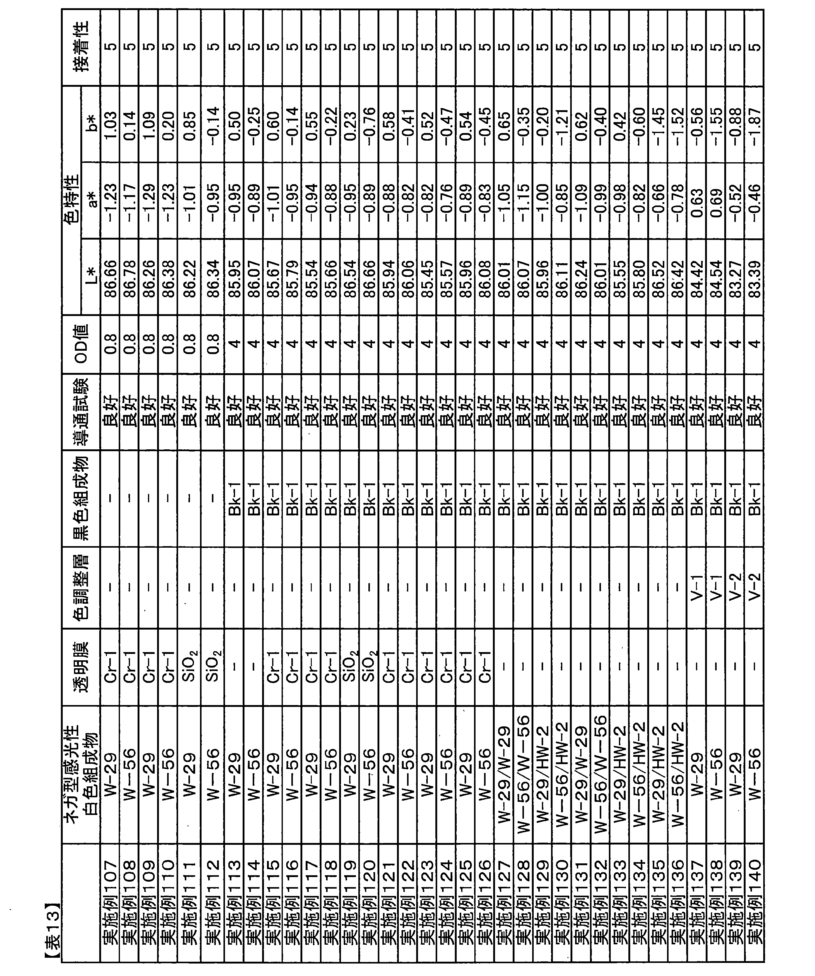
b:透明電極形成後の上面図
c:絶縁膜形成後の上面図
d:金属配線形成後の上面図
1:ガラス基板
2:白色遮光硬化膜
2-1:白色遮光硬化膜(1層目)
2-2:白色遮光硬化膜(2層目)
3:透明電極
4:透明絶縁膜
5:配線電極
6:透明膜
7:黒色遮光性硬化膜
8:色調整層
Claims (20)
- (A)白色顔料、(B)アルカリ可溶性樹脂、(C)多官能モノマー及び(D)光重合開始剤を含有する、タッチパネル用ネガ型感光性白色組成物。
- 前記(B)アルカリ可溶性樹脂として、(b-1)シロキサン樹脂を含有する、請求項1記載のタッチパネル用ネガ型感光性白色組成物。
- 前記(B)アルカリ可溶性樹脂として、(b-2)アクリル樹脂を含有する、請求項1又は2記載のタッチパネル用ネガ型感光性白色組成物。
- さらに(E)チオール化合物を含有する、請求項1~3のいずれか一項記載のタッチパネル用ネガ型感光性白色組成物。
- 前記(A)白色顔料として、酸化チタンを含有する、請求項1~4のいずれか一項記載のタッチパネル用ネガ型感光性白色組成物。
- 前記(C)多官能モノマーとして、下記一般式(1)で表される構造を有する化合物、及び/又は、下記一般式(2)で表される構造を有する化合物を含有する、請求項1~5のいずれか一項記載のタッチパネル用ネガ型感光性白色組成物。


- 前記(D)光重合開始剤として、アシルホスフィンオキサイド系光重合開始剤を含有する、請求項1~6のいずれか一項記載のタッチパネル用ネガ型感光性白色組成物。
- さらに(F)酸化防止剤を含有する、請求項1~7のいずれか一項記載のタッチパネル用ネガ型感光性白色組成物。
- さらに下記一般式(3)で表される(G)シランカップリング剤を含有する、請求項1~8のいずれか一項記載のタッチパネル用ネガ型感光性白色組成物。
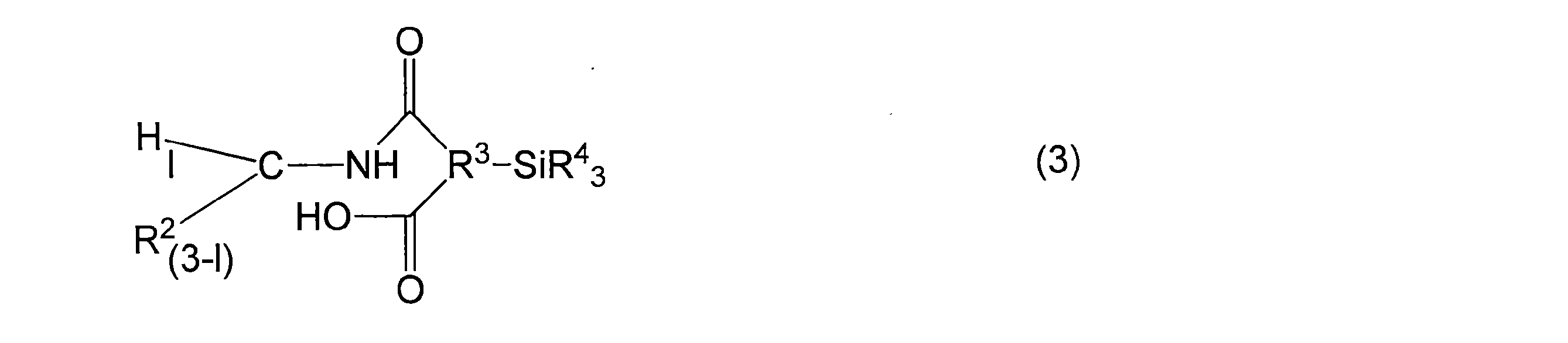
- さらに(H)紫外線吸収剤を含有する、請求項1~9のいずれか一項記載のタッチパネル用ネガ型感光性白色組成物。
- さらに(I)着色剤を含有する、請求項1~10のいずれか一項記載のタッチパネル用ネガ型感光性白色組成物。
- 請求項1~11のいずれか一項記載のタッチパネル用ネガ型感光性白色組成物を硬化させてなる白色遮光性硬化膜パターンを具備する、タッチパネル。
- 請求項1~11のいずれか一項記載のタッチパネル用ネガ型感光性白色組成物を用いて白色遮光性硬化膜パターンを形成する工程を備える、タッチパネルの製造方法。
- 前記白色遮光性硬化膜パターンを形成する工程を複数回以上備える、請求項13記載のタッチパネルの製造方法。
- 前記白色遮光性硬化膜パターンを形成する工程をn回繰り返した時、第n層(nは2以上の整数)は第n-1層よりも線幅を広く、膜厚を薄く形成する工程である、請求項14記載のタッチパネルの製造方法。
- 前記白色遮光性硬化膜パターンを形成する工程、及び、非感光性白色組成物のパターン印刷による硬化膜形成工程を少なくともそれぞれ1回以上備える、請求項13または14記載のタッチパネルの製造方法。
- さらに、前記白色遮光性硬化膜パターンの上部に黒色光性硬化膜を形成する工程を備える、請求項13~16のいずれか一項記載のタッチパネルの製造方法。
- さらに、前記白色遮光性硬化膜パターンの上部に透明膜を形成する工程を備える、請求項13~17のいずれか一項記載のタッチパネルの製造方法。
- さらに、前記白色遮光性硬化膜パターンの上部に色調整層を形成する工程を備える、請求項13~18のいずれか一項記載のタッチパネルの製造方法。
- さらに、前記白色遮光性硬化膜パターンの下部に色調整層を形成する工程を備える、請求項13~19のいずれか一項記載のタッチパネルの製造方法。
Priority Applications (4)
| Application Number | Priority Date | Filing Date | Title |
|---|---|---|---|
| US14/907,137 US9690197B2 (en) | 2013-07-25 | 2014-07-18 | Negative-type photosensitive white composition for touch panel, touch panel and touch panel production method |
| JP2014537200A JP6635497B2 (ja) | 2013-07-25 | 2014-07-18 | タッチパネル用ネガ型感光性白色組成物、タッチパネル及びタッチパネルの製造方法 |
| CN201480041963.4A CN105378615B (zh) | 2013-07-25 | 2014-07-18 | 触控面板用负型感光性白色组合物、触控面板及触控面板的制造方法 |
| KR1020167001777A KR102082722B1 (ko) | 2013-07-25 | 2014-07-18 | 터치 패널용 네거티브형 감광성 백색 조성물, 터치 패널 및 터치 패널의 제조 방법 |
Applications Claiming Priority (2)
| Application Number | Priority Date | Filing Date | Title |
|---|---|---|---|
| JP2013154333 | 2013-07-25 | ||
| JP2013-154333 | 2013-07-25 |
Publications (1)
| Publication Number | Publication Date |
|---|---|
| WO2015012228A1 true WO2015012228A1 (ja) | 2015-01-29 |
Family
ID=52393267
Family Applications (1)
| Application Number | Title | Priority Date | Filing Date |
|---|---|---|---|
| PCT/JP2014/069221 Ceased WO2015012228A1 (ja) | 2013-07-25 | 2014-07-18 | タッチパネル用ネガ型感光性白色組成物、タッチパネル及びタッチパネルの製造方法 |
Country Status (6)
| Country | Link |
|---|---|
| US (1) | US9690197B2 (ja) |
| JP (1) | JP6635497B2 (ja) |
| KR (1) | KR102082722B1 (ja) |
| CN (1) | CN105378615B (ja) |
| TW (1) | TWI638234B (ja) |
| WO (1) | WO2015012228A1 (ja) |
Cited By (28)
| Publication number | Priority date | Publication date | Assignee | Title |
|---|---|---|---|---|
| JP2014160228A (ja) * | 2013-01-22 | 2014-09-04 | Toyo Ink Sc Holdings Co Ltd | 感光性樹脂組成物、ならびにそれを用いた塗膜 |
| JP2015069085A (ja) * | 2013-09-30 | 2015-04-13 | 新日鉄住金化学株式会社 | 白色感光性樹脂組成物、それを用いた硬化物、及びその硬化物を構成成分として含むタッチパネル |
| JP2015072468A (ja) * | 2013-09-05 | 2015-04-16 | 三洋化成工業株式会社 | 感光性樹脂組成物 |
| WO2015133599A1 (ja) * | 2014-03-07 | 2015-09-11 | 富士フイルム株式会社 | 加飾材付き基材およびその製造方法、タッチパネル、ならびに情報表示装置 |
| JP2016151829A (ja) * | 2015-02-16 | 2016-08-22 | 大日本印刷株式会社 | タッチパネル |
| JP2017044976A (ja) * | 2015-08-28 | 2017-03-02 | 三洋化成工業株式会社 | 感光性樹脂組成物 |
| WO2017057543A1 (ja) * | 2015-09-30 | 2017-04-06 | 東レ株式会社 | 感光性樹脂組成物、硬化膜、タッチパネル及びタッチパネルの製造方法 |
| WO2017090680A1 (ja) * | 2015-11-24 | 2017-06-01 | 積水化学工業株式会社 | 硬化性組成物及び電子部品の製造方法 |
| JP2017119735A (ja) * | 2015-12-28 | 2017-07-06 | 山陽色素株式会社 | 金属酸化物用分散剤、これを用いた金属酸化物分散体及びシリコーン重合体組成物並びにこれらの製造方法 |
| JP2017119772A (ja) * | 2015-12-28 | 2017-07-06 | 積水化学工業株式会社 | 光硬化性組成物及び電子部品の製造方法 |
| WO2017140409A1 (en) * | 2016-02-19 | 2017-08-24 | Az Electronic Materials (Luxembourg) S.À. R.L. | Negative type photosensitive composition curable at low temperature |
| JP2017151321A (ja) * | 2016-02-25 | 2017-08-31 | 富士フイルム株式会社 | 硬化性組成物、硬化膜の製造方法、硬化膜、タッチパネル及び表示装置 |
| WO2017167690A1 (en) * | 2016-03-30 | 2017-10-05 | Az Electronic Materials (Luxembourg) S.A.R.L. | Negative type photosensitive composition curable at low temperature |
| JP2017186488A (ja) * | 2016-04-08 | 2017-10-12 | 山陽色素株式会社 | 蛍光顔料分散体および白色積層体 |
| WO2017208848A1 (ja) * | 2016-05-31 | 2017-12-07 | 富士フイルム株式会社 | 感光性樹脂組成物、転写フィルム、加飾パターン、及びタッチパネル |
| JP2018097378A (ja) * | 2013-09-25 | 2018-06-21 | 三菱ケミカル株式会社 | 感光性着色組成物、硬化物、ブラックマトリクス、着色スペーサー及び画像表示装置 |
| JP2018189877A (ja) * | 2017-05-10 | 2018-11-29 | 株式会社Adeka | 重合性組成物、ブラックマトリクス用感光性組成物及び硬化物 |
| WO2019026458A1 (ja) * | 2017-08-02 | 2019-02-07 | 東レ株式会社 | シロキサン樹脂組成物、それを用いた接着剤、表示装置、半導体装置および照明装置 |
| JP2019046790A (ja) * | 2017-09-05 | 2019-03-22 | Jsr株式会社 | 表示素子形成用感光性組成物、硬化膜および表示素子 |
| WO2019176785A1 (ja) * | 2018-03-14 | 2019-09-19 | 東レ株式会社 | ネガ型感光性着色組成物、硬化膜、それを用いたタッチパネル |
| WO2020008969A1 (ja) * | 2018-07-05 | 2020-01-09 | 東レ株式会社 | 樹脂組成物、遮光膜、遮光膜の製造方法および隔壁付き基板 |
| JP2020067636A (ja) * | 2018-10-26 | 2020-04-30 | 旭化成株式会社 | 感光性樹脂組成物、感光性樹脂積層体、パターン製造方法及び硬化膜パターン製造方法 |
| JPWO2021049401A1 (ja) * | 2019-09-11 | 2021-03-18 | ||
| JP2021103294A (ja) * | 2019-12-24 | 2021-07-15 | ローム・アンド・ハース・エレクトロニック・マテリアルズ・コリア・リミテッド | 着色感光性樹脂組成物及びそれから製造されるブラックマトリクス |
| CN114479559A (zh) * | 2020-11-12 | 2022-05-13 | 宸鸿科技(厦门)有限公司 | 形成绝缘层的墨水组成物、方法和触控面板 |
| WO2022270118A1 (ja) * | 2021-06-22 | 2022-12-29 | 信越化学工業株式会社 | 感光性樹脂組成物、感光性樹脂皮膜、感光性ドライフィルム及びパターン形成方法 |
| WO2024204759A1 (ja) * | 2023-03-30 | 2024-10-03 | 太陽ホールディングス株式会社 | 感光性熱硬化性樹脂組成物、ドライフィルム、硬化物及び電子部品 |
| WO2025052998A1 (ja) * | 2023-09-08 | 2025-03-13 | 富士フイルム株式会社 | 硬化性組成物、硬化物および光学部材 |
Families Citing this family (22)
| Publication number | Priority date | Publication date | Assignee | Title |
|---|---|---|---|---|
| TWI549027B (zh) * | 2014-04-22 | 2016-09-11 | 群創光電股份有限公司 | 觸控面板及觸控顯示裝置 |
| CN104360785A (zh) * | 2014-12-02 | 2015-02-18 | 合肥鑫晟光电科技有限公司 | 一种触摸屏面板、触摸屏及显示装置 |
| WO2017150093A1 (ja) * | 2016-02-29 | 2017-09-08 | 富士フイルム株式会社 | 組成物、組成物の製造方法、硬化膜、カラーフィルタ、遮光膜、固体撮像素子および画像表示装置 |
| TWI691794B (zh) * | 2016-09-29 | 2020-04-21 | 奇美實業股份有限公司 | 負型白色感光性樹脂組成物及其應用 |
| WO2018061525A1 (ja) * | 2016-09-30 | 2018-04-05 | 東レ株式会社 | ネガ型感光性樹脂組成物、硬化膜、硬化膜を具備する素子及び表示装置、並びにその製造方法 |
| CN107957655A (zh) * | 2016-10-18 | 2018-04-24 | 广州亦盛环保科技有限公司 | 一种3d盖板玻璃用负型感光性白色油墨及其制备方法、使用方法 |
| JP6872113B2 (ja) * | 2016-12-08 | 2021-05-19 | 富士フイルムビジネスイノベーション株式会社 | トナーセット、現像剤セット、トナーカートリッジセット、画像形成装置及び画像形成方法 |
| JP7274496B2 (ja) | 2018-03-23 | 2023-05-16 | メルク パテント ゲゼルシャフト ミット ベシュレンクテル ハフツング | ネガ作動型超厚膜フォトレジスト |
| KR102383696B1 (ko) * | 2018-03-30 | 2022-04-05 | 동우 화인켐 주식회사 | 감광성 수지 조성물 및 이로부터 형성된 광경화성 보호막 |
| CN112292638B (zh) | 2018-04-24 | 2024-06-11 | 美国陶氏有机硅公司 | 正色调可光图案化有机硅 |
| KR20190136248A (ko) * | 2018-05-30 | 2019-12-10 | 롬엔드하스전자재료코리아유한회사 | 포지티브형 감광성 수지 조성물 및 이를 이용한 경화막 |
| JPWO2020070924A1 (ja) | 2018-10-03 | 2021-09-24 | Hdマイクロシステムズ株式会社 | 感光性樹脂組成物、パターン硬化物の製造方法、硬化物、層間絶縁膜、カバーコート層、表面保護膜及び電子部品 |
| JP7213675B2 (ja) * | 2018-12-21 | 2023-01-27 | 東京応化工業株式会社 | ネガ型感光性樹脂組成物、感光性レジストフィルム、パターン形成方法 |
| CN109856913A (zh) * | 2019-01-29 | 2019-06-07 | 晟光科技股份有限公司 | 一种应用于ogs触摸屏的光刻胶及其光刻工艺 |
| JP2021026029A (ja) | 2019-07-31 | 2021-02-22 | メルク、パテント、ゲゼルシャフト、ミット、ベシュレンクテル、ハフツングMerck Patent GmbH | ネガ型感光性組成物 |
| TWI732580B (zh) * | 2020-06-03 | 2021-07-01 | 新應材股份有限公司 | 感光性樹脂組成物、隔壁、光轉換層以及光發射裝置 |
| CN113759661B (zh) * | 2020-06-03 | 2024-10-22 | 新应材股份有限公司 | 感光性树脂组合物、隔壁、光转换层以及光发射装置 |
| TWI767248B (zh) * | 2020-06-10 | 2022-06-11 | 新應材股份有限公司 | 白色感光性樹脂組成物、白色隔壁、光轉換層以及光發射裝置 |
| CN113777882B (zh) * | 2020-06-10 | 2025-03-07 | 新应材股份有限公司 | 白色感光性树脂组合物、白色隔壁、光转换层以及光发射装置 |
| US20220163887A1 (en) * | 2020-11-24 | 2022-05-26 | Rohm And Haas Electronic Materials Korea Ltd. | Colored photosensitive resin composition and multilayer cured film prepared therefrom |
| US11650705B2 (en) * | 2020-12-07 | 2023-05-16 | Tpk Advanced Solutions Inc. | Touch panel, electronic device and manufacture method thereof |
| EP4579339A3 (en) * | 2023-12-29 | 2025-09-03 | Duksan Neolux Co., Ltd | Pixel define layer |
Citations (12)
| Publication number | Priority date | Publication date | Assignee | Title |
|---|---|---|---|---|
| JP2004287227A (ja) * | 2003-03-24 | 2004-10-14 | Dainippon Printing Co Ltd | 感光性パターン形成用硬化性樹脂組成物、液晶パネル用基板、及び、液晶パネル |
| JP2010276916A (ja) * | 2009-05-29 | 2010-12-09 | Toyobo Co Ltd | 感光性凸版印刷原版 |
| JP2011095716A (ja) * | 2009-09-29 | 2011-05-12 | Fujifilm Corp | 着色感光性樹脂組成物、着色樹脂パターンの製造方法、カラーフィルター、および液晶表示装置 |
| WO2011111748A1 (ja) * | 2010-03-11 | 2011-09-15 | アルプス電気株式会社 | 透光型入力装置 |
| JP2012088934A (ja) * | 2010-10-20 | 2012-05-10 | Alps Electric Co Ltd | 入力装置及び入力装置の製造方法 |
| JP2012098785A (ja) * | 2010-10-29 | 2012-05-24 | Alps Electric Co Ltd | 入力装置の製造方法 |
| WO2013031753A1 (ja) * | 2011-08-29 | 2013-03-07 | 東レ株式会社 | 着色樹脂組成物及び樹脂ブラックマトリクス基板 |
| WO2013047553A1 (ja) * | 2011-09-30 | 2013-04-04 | 富士フイルム株式会社 | 静電容量型入力装置の製造方法および静電容量型入力装置、並びに、これを備えた画像表示装置 |
| JP2013152639A (ja) * | 2012-01-25 | 2013-08-08 | Dainippon Printing Co Ltd | 表示装置用前面保護板、及び表示装置 |
| WO2013137226A1 (ja) * | 2012-03-15 | 2013-09-19 | 富士フイルム株式会社 | 感光性フィルム、静電容量型入力装置の製造方法および静電容量型入力装置、並びに、これを備えた画像表示装置 |
| JP2014123340A (ja) * | 2012-12-21 | 2014-07-03 | Samsung Electro-Mechanics Co Ltd | タッチパネル |
| JP2014146283A (ja) * | 2013-01-30 | 2014-08-14 | Toppan Printing Co Ltd | 前面板一体型タッチパネルセンサー基板及び表示装置 |
Family Cites Families (16)
| Publication number | Priority date | Publication date | Assignee | Title |
|---|---|---|---|---|
| KR0140908B1 (ko) * | 1995-01-20 | 1998-06-15 | 박흥기 | 액정 디스플레이 칼라필터용 안료분산 포토 레지스트 조성물 |
| JP2004198717A (ja) * | 2002-12-18 | 2004-07-15 | Showa Denko Kk | カラーフィルターブラックマトリックスレジスト組成物及びその組成物に用いるカーボンブラック分散液組成物 |
| WO2004086145A1 (ja) * | 2003-03-24 | 2004-10-07 | Dai Nippon Printing Co. Ltd. | 硬化性樹脂組成物、感光性パターン形成用硬化性樹脂組成物、カラーフィルター、液晶パネル用基板、及び、液晶パネル |
| JP4832973B2 (ja) * | 2006-07-26 | 2011-12-07 | 富士フイルム株式会社 | カラーフィルタ用硬化性組成物、カラーフィルタ、及びその製造方法 |
| JP5023878B2 (ja) * | 2006-08-11 | 2012-09-12 | 住友化学株式会社 | 重合性樹脂組成物 |
| JP2008151245A (ja) * | 2006-12-16 | 2008-07-03 | Kaneko Denki Kk | 結束バンド並びにその固定方法及び固定治具 |
| JP5236238B2 (ja) * | 2007-09-28 | 2013-07-17 | 富士フイルム株式会社 | インクジェット記録用ホワイトインク組成物 |
| JP5079487B2 (ja) * | 2007-12-21 | 2012-11-21 | 凸版印刷株式会社 | 液晶表示装置およびそれに用いるカラーフィルタ |
| WO2010061744A1 (ja) * | 2008-11-27 | 2010-06-03 | 東レ株式会社 | シロキサン樹脂組成物およびそれを用いたタッチパネル用保護膜 |
| JP5744528B2 (ja) | 2011-01-11 | 2015-07-08 | 東京応化工業株式会社 | タッチパネル用着色感光性樹脂組成物、タッチパネル、及び表示装置 |
| CN102621811B (zh) * | 2011-01-31 | 2017-03-01 | 新应材股份有限公司 | 一种应用于面板结构的可显影感光性树脂组成物 |
| JP2012242928A (ja) | 2011-05-17 | 2012-12-10 | Toppan Printing Co Ltd | 加飾透明保護基板一体型タッチパネル |
| JP5734913B2 (ja) * | 2011-08-31 | 2015-06-17 | 富士フイルム株式会社 | 感放射線性組成物、パターン形成方法、カラーフィルタ及びその製造方法、並びに、固体撮像素子 |
| CN104471481B (zh) * | 2012-05-30 | 2019-04-19 | 株式会社Lg化学 | 光敏树脂组合物和包含通过使用其制备的边框图案的触摸面板或显示器件 |
| KR20140066417A (ko) * | 2012-11-23 | 2014-06-02 | 삼성전기주식회사 | 터치 스크린 모듈 및 이의 제조방법 |
| CN104969126B (zh) * | 2013-02-14 | 2019-10-01 | 东丽株式会社 | 负型感光性着色组合物、固化膜、触摸面板用遮光图案和触摸面板的制造方法 |
-
2014
- 2014-07-18 JP JP2014537200A patent/JP6635497B2/ja not_active Expired - Fee Related
- 2014-07-18 CN CN201480041963.4A patent/CN105378615B/zh active Active
- 2014-07-18 KR KR1020167001777A patent/KR102082722B1/ko not_active Expired - Fee Related
- 2014-07-18 US US14/907,137 patent/US9690197B2/en not_active Expired - Fee Related
- 2014-07-18 WO PCT/JP2014/069221 patent/WO2015012228A1/ja not_active Ceased
- 2014-07-22 TW TW103125070A patent/TWI638234B/zh active
Patent Citations (12)
| Publication number | Priority date | Publication date | Assignee | Title |
|---|---|---|---|---|
| JP2004287227A (ja) * | 2003-03-24 | 2004-10-14 | Dainippon Printing Co Ltd | 感光性パターン形成用硬化性樹脂組成物、液晶パネル用基板、及び、液晶パネル |
| JP2010276916A (ja) * | 2009-05-29 | 2010-12-09 | Toyobo Co Ltd | 感光性凸版印刷原版 |
| JP2011095716A (ja) * | 2009-09-29 | 2011-05-12 | Fujifilm Corp | 着色感光性樹脂組成物、着色樹脂パターンの製造方法、カラーフィルター、および液晶表示装置 |
| WO2011111748A1 (ja) * | 2010-03-11 | 2011-09-15 | アルプス電気株式会社 | 透光型入力装置 |
| JP2012088934A (ja) * | 2010-10-20 | 2012-05-10 | Alps Electric Co Ltd | 入力装置及び入力装置の製造方法 |
| JP2012098785A (ja) * | 2010-10-29 | 2012-05-24 | Alps Electric Co Ltd | 入力装置の製造方法 |
| WO2013031753A1 (ja) * | 2011-08-29 | 2013-03-07 | 東レ株式会社 | 着色樹脂組成物及び樹脂ブラックマトリクス基板 |
| WO2013047553A1 (ja) * | 2011-09-30 | 2013-04-04 | 富士フイルム株式会社 | 静電容量型入力装置の製造方法および静電容量型入力装置、並びに、これを備えた画像表示装置 |
| JP2013152639A (ja) * | 2012-01-25 | 2013-08-08 | Dainippon Printing Co Ltd | 表示装置用前面保護板、及び表示装置 |
| WO2013137226A1 (ja) * | 2012-03-15 | 2013-09-19 | 富士フイルム株式会社 | 感光性フィルム、静電容量型入力装置の製造方法および静電容量型入力装置、並びに、これを備えた画像表示装置 |
| JP2014123340A (ja) * | 2012-12-21 | 2014-07-03 | Samsung Electro-Mechanics Co Ltd | タッチパネル |
| JP2014146283A (ja) * | 2013-01-30 | 2014-08-14 | Toppan Printing Co Ltd | 前面板一体型タッチパネルセンサー基板及び表示装置 |
Cited By (51)
| Publication number | Priority date | Publication date | Assignee | Title |
|---|---|---|---|---|
| JP2014160228A (ja) * | 2013-01-22 | 2014-09-04 | Toyo Ink Sc Holdings Co Ltd | 感光性樹脂組成物、ならびにそれを用いた塗膜 |
| JP2015072468A (ja) * | 2013-09-05 | 2015-04-16 | 三洋化成工業株式会社 | 感光性樹脂組成物 |
| JP2018097378A (ja) * | 2013-09-25 | 2018-06-21 | 三菱ケミカル株式会社 | 感光性着色組成物、硬化物、ブラックマトリクス、着色スペーサー及び画像表示装置 |
| JP2015069085A (ja) * | 2013-09-30 | 2015-04-13 | 新日鉄住金化学株式会社 | 白色感光性樹脂組成物、それを用いた硬化物、及びその硬化物を構成成分として含むタッチパネル |
| JPWO2015133599A1 (ja) * | 2014-03-07 | 2017-04-06 | 富士フイルム株式会社 | 加飾材付き基材およびその製造方法、タッチパネル、ならびに情報表示装置 |
| WO2015133599A1 (ja) * | 2014-03-07 | 2015-09-11 | 富士フイルム株式会社 | 加飾材付き基材およびその製造方法、タッチパネル、ならびに情報表示装置 |
| JP2016151829A (ja) * | 2015-02-16 | 2016-08-22 | 大日本印刷株式会社 | タッチパネル |
| JP2017044976A (ja) * | 2015-08-28 | 2017-03-02 | 三洋化成工業株式会社 | 感光性樹脂組成物 |
| WO2017057543A1 (ja) * | 2015-09-30 | 2017-04-06 | 東レ株式会社 | 感光性樹脂組成物、硬化膜、タッチパネル及びタッチパネルの製造方法 |
| CN108027565A (zh) * | 2015-09-30 | 2018-05-11 | 东丽株式会社 | 感光性树脂组合物、固化膜、触摸面板及触摸面板的制造方法 |
| WO2017090680A1 (ja) * | 2015-11-24 | 2017-06-01 | 積水化学工業株式会社 | 硬化性組成物及び電子部品の製造方法 |
| JP6145232B1 (ja) * | 2015-11-24 | 2017-06-07 | 積水化学工業株式会社 | 硬化性組成物及び電子部品の製造方法 |
| KR102639455B1 (ko) | 2015-11-24 | 2024-02-23 | 다이요 홀딩스 가부시키가이샤 | 경화성 조성물 및 전자 부품의 제조 방법 |
| KR20180087137A (ko) * | 2015-11-24 | 2018-08-01 | 세키스이가가쿠 고교가부시키가이샤 | 경화성 조성물 및 전자 부품의 제조 방법 |
| CN107531815A (zh) * | 2015-11-24 | 2018-01-02 | 积水化学工业株式会社 | 固化性组合物及电子部件的制造方法 |
| JP2017119735A (ja) * | 2015-12-28 | 2017-07-06 | 山陽色素株式会社 | 金属酸化物用分散剤、これを用いた金属酸化物分散体及びシリコーン重合体組成物並びにこれらの製造方法 |
| JP2017119772A (ja) * | 2015-12-28 | 2017-07-06 | 積水化学工業株式会社 | 光硬化性組成物及び電子部品の製造方法 |
| KR20180112052A (ko) * | 2016-02-19 | 2018-10-11 | 에이제트 일렉트로닉 머티어리얼스 (룩셈부르크) 에스.에이.알.엘. | 저온 경화 가능한 네거티브형 감광성 조성물 |
| KR102374190B1 (ko) | 2016-02-19 | 2022-03-15 | 에이제트 일렉트로닉 머티어리얼스 (룩셈부르크) 에스.에이.알.엘. | 저온 경화 가능한 네거티브형 감광성 조성물 |
| US11630390B2 (en) | 2016-02-19 | 2023-04-18 | Merck Patent Gmbh | Negative type photosensitive composition curable at low temperature |
| WO2017140409A1 (en) * | 2016-02-19 | 2017-08-24 | Az Electronic Materials (Luxembourg) S.À. R.L. | Negative type photosensitive composition curable at low temperature |
| JP2017151321A (ja) * | 2016-02-25 | 2017-08-31 | 富士フイルム株式会社 | 硬化性組成物、硬化膜の製造方法、硬化膜、タッチパネル及び表示装置 |
| WO2017167690A1 (en) * | 2016-03-30 | 2017-10-05 | Az Electronic Materials (Luxembourg) S.A.R.L. | Negative type photosensitive composition curable at low temperature |
| US11506978B2 (en) | 2016-03-30 | 2022-11-22 | Merck Patent Gmbh | Negative type photosensitive composition curable at low temperature |
| JP2017186488A (ja) * | 2016-04-08 | 2017-10-12 | 山陽色素株式会社 | 蛍光顔料分散体および白色積層体 |
| WO2017208848A1 (ja) * | 2016-05-31 | 2017-12-07 | 富士フイルム株式会社 | 感光性樹脂組成物、転写フィルム、加飾パターン、及びタッチパネル |
| JPWO2017208848A1 (ja) * | 2016-05-31 | 2019-02-14 | 富士フイルム株式会社 | 感光性樹脂組成物、転写フィルム、加飾パターン、及びタッチパネル |
| US11500286B2 (en) | 2016-05-31 | 2022-11-15 | Fujifilm Corporation | Photosensitive resin composition, transfer film, decorative pattern, and touch panel |
| JP7049067B2 (ja) | 2017-05-10 | 2022-04-06 | 株式会社Adeka | 重合性組成物、ブラックマトリクス用感光性組成物及び硬化物 |
| JP2018189877A (ja) * | 2017-05-10 | 2018-11-29 | 株式会社Adeka | 重合性組成物、ブラックマトリクス用感光性組成物及び硬化物 |
| WO2019026458A1 (ja) * | 2017-08-02 | 2019-02-07 | 東レ株式会社 | シロキサン樹脂組成物、それを用いた接着剤、表示装置、半導体装置および照明装置 |
| US11319445B2 (en) | 2017-08-02 | 2022-05-03 | Toray Industries, Inc. | Siloxane resin composition, adhesive using same, display device, semiconductor device, and illumination device |
| JP2019046790A (ja) * | 2017-09-05 | 2019-03-22 | Jsr株式会社 | 表示素子形成用感光性組成物、硬化膜および表示素子 |
| JP7047642B2 (ja) | 2017-09-05 | 2022-04-05 | Jsr株式会社 | 隔壁形成用感光性組成物、隔壁および表示素子 |
| KR20200132843A (ko) | 2018-03-14 | 2020-11-25 | 도레이 카부시키가이샤 | 네거티브형 감광성 착색 조성물, 경화막, 그것을 이용한 터치 패널 |
| WO2019176785A1 (ja) * | 2018-03-14 | 2019-09-19 | 東レ株式会社 | ネガ型感光性着色組成物、硬化膜、それを用いたタッチパネル |
| CN111771163A (zh) * | 2018-03-14 | 2020-10-13 | 东丽株式会社 | 负型感光性着色组合物、固化膜、使用了它们的触摸面板 |
| WO2020008969A1 (ja) * | 2018-07-05 | 2020-01-09 | 東レ株式会社 | 樹脂組成物、遮光膜、遮光膜の製造方法および隔壁付き基板 |
| JPWO2020008969A1 (ja) * | 2018-07-05 | 2021-05-13 | 東レ株式会社 | 樹脂組成物、遮光膜および遮光膜の製造方法 |
| JP2020067636A (ja) * | 2018-10-26 | 2020-04-30 | 旭化成株式会社 | 感光性樹脂組成物、感光性樹脂積層体、パターン製造方法及び硬化膜パターン製造方法 |
| JP7218149B2 (ja) | 2018-10-26 | 2023-02-06 | 旭化成株式会社 | 感光性樹脂組成物、感光性樹脂積層体、パターン製造方法及び硬化膜パターン製造方法 |
| JP7063391B2 (ja) | 2019-09-11 | 2022-05-09 | 東レ株式会社 | 感光性樹脂組成物、硬化膜および表示装置 |
| KR20220063160A (ko) * | 2019-09-11 | 2022-05-17 | 도레이 카부시키가이샤 | 감광성 수지 조성물, 경화막 및 표시 장치 |
| WO2021049401A1 (ja) * | 2019-09-11 | 2021-03-18 | 東レ株式会社 | 感光性樹脂組成物、硬化膜および表示装置 |
| JPWO2021049401A1 (ja) * | 2019-09-11 | 2021-03-18 | ||
| KR102556723B1 (ko) | 2019-09-11 | 2023-07-18 | 도레이 카부시키가이샤 | 감광성 수지 조성물, 경화막 및 표시 장치 |
| JP2021103294A (ja) * | 2019-12-24 | 2021-07-15 | ローム・アンド・ハース・エレクトロニック・マテリアルズ・コリア・リミテッド | 着色感光性樹脂組成物及びそれから製造されるブラックマトリクス |
| CN114479559A (zh) * | 2020-11-12 | 2022-05-13 | 宸鸿科技(厦门)有限公司 | 形成绝缘层的墨水组成物、方法和触控面板 |
| WO2022270118A1 (ja) * | 2021-06-22 | 2022-12-29 | 信越化学工業株式会社 | 感光性樹脂組成物、感光性樹脂皮膜、感光性ドライフィルム及びパターン形成方法 |
| WO2024204759A1 (ja) * | 2023-03-30 | 2024-10-03 | 太陽ホールディングス株式会社 | 感光性熱硬化性樹脂組成物、ドライフィルム、硬化物及び電子部品 |
| WO2025052998A1 (ja) * | 2023-09-08 | 2025-03-13 | 富士フイルム株式会社 | 硬化性組成物、硬化物および光学部材 |
Also Published As
| Publication number | Publication date |
|---|---|
| KR102082722B1 (ko) | 2020-02-28 |
| US20160161847A1 (en) | 2016-06-09 |
| KR20160034907A (ko) | 2016-03-30 |
| CN105378615B (zh) | 2019-05-31 |
| JPWO2015012228A1 (ja) | 2017-03-02 |
| US9690197B2 (en) | 2017-06-27 |
| JP6635497B2 (ja) | 2020-01-29 |
| TW201510665A (zh) | 2015-03-16 |
| CN105378615A (zh) | 2016-03-02 |
| TWI638234B (zh) | 2018-10-11 |
Similar Documents
| Publication | Publication Date | Title |
|---|---|---|
| JP6635497B2 (ja) | タッチパネル用ネガ型感光性白色組成物、タッチパネル及びタッチパネルの製造方法 | |
| JP6201984B2 (ja) | ネガ型感光性着色組成物、硬化膜、タッチパネル用遮光パターン及びタッチパネルの製造方法 | |
| KR102028970B1 (ko) | 금속산화물 감광성 수지 조성물, 이를 이용하여 제조된 컬러필터 및 화상 표시 장치 | |
| TWI607281B (zh) | 觸控面板用黑色感光性組成物及觸控面板 | |
| KR20130070563A (ko) | 네거티브형 감광성 수지 조성물, 그것을 사용한 보호막 및 터치 패널 부재 | |
| JP2011039165A (ja) | アルカリ可溶性光硬化型組成物、該組成物を使用した硬化塗膜及び透明部材 | |
| WO2007061115A1 (ja) | 隔壁、カラーフィルタ、有機elの製造方法 | |
| JP2021107928A (ja) | 青色感光性樹脂組成物、これを用いて製造されたカラーフィルタおよび画像表示装置 | |
| WO2011129312A1 (ja) | ネガ型感光性樹脂組成物、硬化膜、およびタッチパネル用部材 | |
| JP2021161401A (ja) | 樹脂組成物、遮光膜、遮光膜の製造方法および隔壁付き基板 | |
| JP2025120301A (ja) | 感光性樹脂組成物、硬化膜、硬化膜付き基板、硬化膜付き基板の製造方法および表示装置 | |
| JP2017068007A (ja) | 感光性樹脂組成物 | |
| WO2023048016A1 (ja) | 樹脂組成物、遮光膜、および隔壁付き基板 | |
| CN113474730B (zh) | 负型感光性树脂组合物、使用它的固化膜的制造方法及触控面板 | |
| CN105717743A (zh) | 感光性树脂组合物及其应用 | |
| US10877607B2 (en) | Laminated base material, cover glass, touch panel, and method for manufacturing laminated base material | |
| JP7742233B2 (ja) | 感光性樹脂およびそれを用いた感光性樹脂組成物、並びにその硬化物およびカラーフィルター | |
| JP2019124929A (ja) | ネガ型感光性樹脂組成物、それを用いたフォトスペーサーおよび画像表示装置 | |
| TW201716870A (zh) | 感光性樹脂組成物、硬化膜、觸控面板及觸控面板之製造方法 | |
| JP7853842B2 (ja) | 感光性樹脂組成物、硬化膜、ディスプレイ構成要素および表示装置 | |
| CN110268328A (zh) | 蓝色感光性树脂组合物、利用该组合物制造的滤色器及图像显示装置 | |
| JP2019164341A (ja) | ネガ型感光性樹脂組成物、それを用いたフォトスペーサーおよび画像表示装置 |
Legal Events
| Date | Code | Title | Description |
|---|---|---|---|
| ENP | Entry into the national phase |
Ref document number: 2014537200 Country of ref document: JP Kind code of ref document: A |
|
| 121 | Ep: the epo has been informed by wipo that ep was designated in this application |
Ref document number: 14830002 Country of ref document: EP Kind code of ref document: A1 |
|
| ENP | Entry into the national phase |
Ref document number: 20167001777 Country of ref document: KR Kind code of ref document: A |
|
| WWE | Wipo information: entry into national phase |
Ref document number: 14907137 Country of ref document: US |
|
| NENP | Non-entry into the national phase |
Ref country code: DE |
|
| 122 | Ep: pct application non-entry in european phase |
Ref document number: 14830002 Country of ref document: EP Kind code of ref document: A1 |