WO2014208341A1 - 反射電極用または配線電極用Ag合金膜、反射電極または配線電極、およびAg合金スパッタリングターゲット - Google Patents
反射電極用または配線電極用Ag合金膜、反射電極または配線電極、およびAg合金スパッタリングターゲット Download PDFInfo
- Publication number
- WO2014208341A1 WO2014208341A1 PCT/JP2014/065518 JP2014065518W WO2014208341A1 WO 2014208341 A1 WO2014208341 A1 WO 2014208341A1 JP 2014065518 W JP2014065518 W JP 2014065518W WO 2014208341 A1 WO2014208341 A1 WO 2014208341A1
- Authority
- WO
- WIPO (PCT)
- Prior art keywords
- film
- alloy film
- alloy
- atomic
- electrode
- Prior art date
- Legal status (The legal status is an assumption and is not a legal conclusion. Google has not performed a legal analysis and makes no representation as to the accuracy of the status listed.)
- Ceased
Links
Images


Classifications
-
- H—ELECTRICITY
- H01—ELECTRIC ELEMENTS
- H01B—CABLES; CONDUCTORS; INSULATORS; SELECTION OF MATERIALS FOR THEIR CONDUCTIVE, INSULATING OR DIELECTRIC PROPERTIES
- H01B1/00—Conductors or conductive bodies characterised by the conductive materials; Selection of materials as conductors
- H01B1/02—Conductors or conductive bodies characterised by the conductive materials; Selection of materials as conductors mainly consisting of metals or alloys
-
- C—CHEMISTRY; METALLURGY
- C22—METALLURGY; FERROUS OR NON-FERROUS ALLOYS; TREATMENT OF ALLOYS OR NON-FERROUS METALS
- C22C—ALLOYS
- C22C5/00—Alloys based on noble metals
- C22C5/06—Alloys based on silver
-
- C—CHEMISTRY; METALLURGY
- C22—METALLURGY; FERROUS OR NON-FERROUS ALLOYS; TREATMENT OF ALLOYS OR NON-FERROUS METALS
- C22F—CHANGING THE PHYSICAL STRUCTURE OF NON-FERROUS METALS AND NON-FERROUS ALLOYS
- C22F1/00—Changing the physical structure of non-ferrous metals or alloys by heat treatment or by hot or cold working
- C22F1/14—Changing the physical structure of non-ferrous metals or alloys by heat treatment or by hot or cold working of noble metals or alloys based thereon
-
- C—CHEMISTRY; METALLURGY
- C23—COATING METALLIC MATERIAL; COATING MATERIAL WITH METALLIC MATERIAL; CHEMICAL SURFACE TREATMENT; DIFFUSION TREATMENT OF METALLIC MATERIAL; COATING BY VACUUM EVAPORATION, BY SPUTTERING, BY ION IMPLANTATION OR BY CHEMICAL VAPOUR DEPOSITION, IN GENERAL; INHIBITING CORROSION OF METALLIC MATERIAL OR INCRUSTATION IN GENERAL
- C23C—COATING METALLIC MATERIAL; COATING MATERIAL WITH METALLIC MATERIAL; SURFACE TREATMENT OF METALLIC MATERIAL BY DIFFUSION INTO THE SURFACE, BY CHEMICAL CONVERSION OR SUBSTITUTION; COATING BY VACUUM EVAPORATION, BY SPUTTERING, BY ION IMPLANTATION OR BY CHEMICAL VAPOUR DEPOSITION, IN GENERAL
- C23C14/00—Coating by vacuum evaporation, by sputtering or by ion implantation of the coating forming material
- C23C14/06—Coating by vacuum evaporation, by sputtering or by ion implantation of the coating forming material characterised by the coating material
- C23C14/08—Oxides
- C23C14/086—Oxides of zinc, germanium, cadmium, indium, tin, thallium or bismuth
-
- C—CHEMISTRY; METALLURGY
- C23—COATING METALLIC MATERIAL; COATING MATERIAL WITH METALLIC MATERIAL; CHEMICAL SURFACE TREATMENT; DIFFUSION TREATMENT OF METALLIC MATERIAL; COATING BY VACUUM EVAPORATION, BY SPUTTERING, BY ION IMPLANTATION OR BY CHEMICAL VAPOUR DEPOSITION, IN GENERAL; INHIBITING CORROSION OF METALLIC MATERIAL OR INCRUSTATION IN GENERAL
- C23C—COATING METALLIC MATERIAL; COATING MATERIAL WITH METALLIC MATERIAL; SURFACE TREATMENT OF METALLIC MATERIAL BY DIFFUSION INTO THE SURFACE, BY CHEMICAL CONVERSION OR SUBSTITUTION; COATING BY VACUUM EVAPORATION, BY SPUTTERING, BY ION IMPLANTATION OR BY CHEMICAL VAPOUR DEPOSITION, IN GENERAL
- C23C14/00—Coating by vacuum evaporation, by sputtering or by ion implantation of the coating forming material
- C23C14/06—Coating by vacuum evaporation, by sputtering or by ion implantation of the coating forming material characterised by the coating material
- C23C14/14—Metallic material, boron or silicon
- C23C14/18—Metallic material, boron or silicon on other inorganic substrates
- C23C14/185—Metallic material, boron or silicon on other inorganic substrates by cathodic sputtering
-
- C—CHEMISTRY; METALLURGY
- C23—COATING METALLIC MATERIAL; COATING MATERIAL WITH METALLIC MATERIAL; CHEMICAL SURFACE TREATMENT; DIFFUSION TREATMENT OF METALLIC MATERIAL; COATING BY VACUUM EVAPORATION, BY SPUTTERING, BY ION IMPLANTATION OR BY CHEMICAL VAPOUR DEPOSITION, IN GENERAL; INHIBITING CORROSION OF METALLIC MATERIAL OR INCRUSTATION IN GENERAL
- C23C—COATING METALLIC MATERIAL; COATING MATERIAL WITH METALLIC MATERIAL; SURFACE TREATMENT OF METALLIC MATERIAL BY DIFFUSION INTO THE SURFACE, BY CHEMICAL CONVERSION OR SUBSTITUTION; COATING BY VACUUM EVAPORATION, BY SPUTTERING, BY ION IMPLANTATION OR BY CHEMICAL VAPOUR DEPOSITION, IN GENERAL
- C23C14/00—Coating by vacuum evaporation, by sputtering or by ion implantation of the coating forming material
- C23C14/22—Coating by vacuum evaporation, by sputtering or by ion implantation of the coating forming material characterised by the process of coating
- C23C14/34—Sputtering
- C23C14/3407—Cathode assembly for sputtering apparatus, e.g. Target
- C23C14/3414—Metallurgical or chemical aspects of target preparation, e.g. casting, powder metallurgy
-
- C—CHEMISTRY; METALLURGY
- C23—COATING METALLIC MATERIAL; COATING MATERIAL WITH METALLIC MATERIAL; CHEMICAL SURFACE TREATMENT; DIFFUSION TREATMENT OF METALLIC MATERIAL; COATING BY VACUUM EVAPORATION, BY SPUTTERING, BY ION IMPLANTATION OR BY CHEMICAL VAPOUR DEPOSITION, IN GENERAL; INHIBITING CORROSION OF METALLIC MATERIAL OR INCRUSTATION IN GENERAL
- C23C—COATING METALLIC MATERIAL; COATING MATERIAL WITH METALLIC MATERIAL; SURFACE TREATMENT OF METALLIC MATERIAL BY DIFFUSION INTO THE SURFACE, BY CHEMICAL CONVERSION OR SUBSTITUTION; COATING BY VACUUM EVAPORATION, BY SPUTTERING, BY ION IMPLANTATION OR BY CHEMICAL VAPOUR DEPOSITION, IN GENERAL
- C23C14/00—Coating by vacuum evaporation, by sputtering or by ion implantation of the coating forming material
- C23C14/58—After-treatment
- C23C14/5806—Thermal treatment
-
- H—ELECTRICITY
- H01—ELECTRIC ELEMENTS
- H01J—ELECTRIC DISCHARGE TUBES OR DISCHARGE LAMPS
- H01J37/00—Discharge tubes with provision for introducing objects or material to be exposed to the discharge, e.g. for the purpose of examination or processing thereof
- H01J37/32—Gas-filled discharge tubes
- H01J37/34—Gas-filled discharge tubes operating with cathodic sputtering
- H01J37/3411—Constructional aspects of the reactor
- H01J37/3414—Targets
- H01J37/3426—Material
- H01J37/3429—Plural materials
-
- H—ELECTRICITY
- H10—SEMICONDUCTOR DEVICES; ELECTRIC SOLID-STATE DEVICES NOT OTHERWISE PROVIDED FOR
- H10W—GENERIC PACKAGES, INTERCONNECTIONS, CONNECTORS OR OTHER CONSTRUCTIONAL DETAILS OF DEVICES COVERED BY CLASS H10
- H10W20/00—Interconnections in chips, wafers or substrates
- H10W20/40—Interconnections external to wafers or substrates, e.g. back-end-of-line [BEOL] metallisations or vias connecting to gate electrodes
- H10W20/41—Interconnections external to wafers or substrates, e.g. back-end-of-line [BEOL] metallisations or vias connecting to gate electrodes characterised by their conductive parts
- H10W20/44—Conductive materials thereof
- H10W20/4403—Conductive materials thereof based on metals, e.g. alloys, metal silicides
- H10W20/4432—Conductive materials thereof based on metals, e.g. alloys, metal silicides the principal metal being a noble metal, e.g. gold
- H10W20/4435—Noble-metal alloys
-
- H—ELECTRICITY
- H10—SEMICONDUCTOR DEVICES; ELECTRIC SOLID-STATE DEVICES NOT OTHERWISE PROVIDED FOR
- H10K—ORGANIC ELECTRIC SOLID-STATE DEVICES
- H10K59/00—Integrated devices, or assemblies of multiple devices, comprising at least one organic light-emitting element covered by group H10K50/00
- H10K59/80—Constructional details
- H10K59/805—Electrodes
- H10K59/8051—Anodes
- H10K59/80518—Reflective anodes, e.g. ITO combined with thick metallic layers
-
- Y—GENERAL TAGGING OF NEW TECHNOLOGICAL DEVELOPMENTS; GENERAL TAGGING OF CROSS-SECTIONAL TECHNOLOGIES SPANNING OVER SEVERAL SECTIONS OF THE IPC; TECHNICAL SUBJECTS COVERED BY FORMER USPC CROSS-REFERENCE ART COLLECTIONS [XRACs] AND DIGESTS
- Y10—TECHNICAL SUBJECTS COVERED BY FORMER USPC
- Y10T—TECHNICAL SUBJECTS COVERED BY FORMER US CLASSIFICATION
- Y10T428/00—Stock material or miscellaneous articles
- Y10T428/12—All metal or with adjacent metals
- Y10T428/12493—Composite; i.e., plural, adjacent, spatially distinct metal components [e.g., layers, joint, etc.]
- Y10T428/12771—Transition metal-base component
- Y10T428/12861—Group VIII or IB metal-base component
- Y10T428/12896—Ag-base component
Definitions
- the Ag alloy film does not form a passive film, and thus is susceptible to external influences. Specifically, it reacts with sulfur to form silver sulfide, or reacts with halogen to form silver halide. There are also disadvantages such as easy aggregation by heating.
- Patent Document 1 discloses that an Ag alloy film containing one or two elements selected from the group consisting of Bi and Sb in a total amount of 0.01 to 4 atomic% is used as an Ag original film. It has been shown that, while maintaining high reflectance, Ag aggregation and crystal grain growth are suppressed, and a decrease in reflectance over time is suppressed.
- this silver oxide is formed is that, as described above, Ag does not form a passive film, and therefore is easily oxidized by the active oxygen generated by the UV irradiation or O 2 plasma.
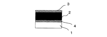
- the Ag alloy film of the present invention that has solved the above-mentioned problems is an Ag alloy film used for a reflective electrode or a wiring electrode, and includes In more than 2.0 atomic% and 2.7 atomic% or less; Zn is 2 It contains at least one of more than 0.0 atomic% and 3.5 atomic% or less.
- the reflective electrode or the wiring electrode of the present invention is such that a transparent conductive film having a film thickness of 5 nm or more and less than 25 nm is formed only directly above the Ag alloy film or directly above and immediately below the Ag alloy film.
- Japanese Patent Application No. 2012-229083 prior to the filing of the present application.
- the upper limit of each content of In and Zn is set to 2.0 from the viewpoint of securing a low electrical resistivity and a high reflectance, which are almost the same level as that of a pure Ag film. Strictly set as atomic%.
- these acceptance criteria are slightly lower than those of the prior application from the viewpoint of ensuring the minimum level applicable to the reflective electrode or the wiring electrode.
- the thickness of the Ag alloy film of the present invention is preferably in the range of 30 to 200 nm.
- the film thickness is preferably in the range of 30 to 200 nm.
- the film thickness is preferably in the range of 30 to 200 nm.
- the Ag alloy film is desirably formed by a sputtering method using a sputtering target.
- the method for forming a thin film include an ink jet coating method, a vacuum deposition method, and a sputtering method.
- the sputtering method is excellent in ease of alloying, productivity, and film thickness uniformity. This is because a homogeneous film can be obtained by uniformly dispersing in the Ag matrix, and the above-described stable characteristics can be obtained.
- a sputtering target containing at least one selected from the above is used. Further, it is preferable to use a sputtering target containing 0.01 to 2.0 atomic% of Bi as the sputtering target.
- the amount of Bi in the formed Ag alloy film decreases with respect to the amount of Bi in the sputtering target. In the present invention, after considering the practical amount of Bi that can be included in the sputtering target, the amount of Bi that is approximately twice the amount of Bi in the Ag alloy film is included in the sputtering target.
- the method for producing the reflective electrode or the wiring electrode of the present invention is not particularly limited, but heat treatment (post-annealing) may be performed after the formation of the transparent conductive film.
- the post-annealing temperature is preferably 200 ° C. or higher, more preferably 250 ° C. or higher, preferably 350 ° C. or lower, more preferably 300 ° C. or lower.
- the post-annealing time is preferably about 10 minutes or more, more preferably about 15 minutes or more, preferably about 120 minutes or less, more preferably about 60 minutes or less.
Landscapes
- Chemical & Material Sciences (AREA)
- Engineering & Computer Science (AREA)
- Organic Chemistry (AREA)
- Materials Engineering (AREA)
- Mechanical Engineering (AREA)
- Metallurgy (AREA)
- Chemical Kinetics & Catalysis (AREA)
- Physics & Mathematics (AREA)
- Thermal Sciences (AREA)
- Crystallography & Structural Chemistry (AREA)
- Inorganic Chemistry (AREA)
- Analytical Chemistry (AREA)
- Plasma & Fusion (AREA)
- Electroluminescent Light Sources (AREA)
- Physical Vapour Deposition (AREA)
- Conductive Materials (AREA)
- Non-Insulated Conductors (AREA)
- Optics & Photonics (AREA)
- General Engineering & Computer Science (AREA)
Priority Applications (4)
| Application Number | Priority Date | Filing Date | Title |
|---|---|---|---|
| US14/889,334 US9947429B2 (en) | 2013-06-26 | 2014-06-11 | Ag alloy film for reflecting electrode or wiring electrode, reflecting electrode or wiring electrode, and Ag alloy sputtering target |
| CN201480035394.2A CN105324510B (zh) | 2013-06-26 | 2014-06-11 | 反射电极用或布线电极用Ag合金膜、反射电极或布线电极、和Ag合金溅射靶 |
| KR1020157036037A KR101764053B1 (ko) | 2013-06-26 | 2014-06-11 | 반사 전극용 또는 배선 전극용 Ag 합금막, 반사 전극 또는 배선 전극, 및 Ag 합금 스퍼터링 타겟 |
| US15/623,975 US20170330643A1 (en) | 2013-06-26 | 2017-06-15 | Ag alloy film for reflecting electrode or wiring electrode, reflecting electrode or wiring electrode, and ag alloy sputtering target |
Applications Claiming Priority (2)
| Application Number | Priority Date | Filing Date | Title |
|---|---|---|---|
| JP2013-134344 | 2013-06-26 | ||
| JP2013134344 | 2013-06-26 |
Related Child Applications (2)
| Application Number | Title | Priority Date | Filing Date |
|---|---|---|---|
| US14/889,334 A-371-Of-International US9947429B2 (en) | 2013-06-26 | 2014-06-11 | Ag alloy film for reflecting electrode or wiring electrode, reflecting electrode or wiring electrode, and Ag alloy sputtering target |
| US15/623,975 Division US20170330643A1 (en) | 2013-06-26 | 2017-06-15 | Ag alloy film for reflecting electrode or wiring electrode, reflecting electrode or wiring electrode, and ag alloy sputtering target |
Publications (1)
| Publication Number | Publication Date |
|---|---|
| WO2014208341A1 true WO2014208341A1 (ja) | 2014-12-31 |
Family
ID=52141685
Family Applications (1)
| Application Number | Title | Priority Date | Filing Date |
|---|---|---|---|
| PCT/JP2014/065518 Ceased WO2014208341A1 (ja) | 2013-06-26 | 2014-06-11 | 反射電極用または配線電極用Ag合金膜、反射電極または配線電極、およびAg合金スパッタリングターゲット |
Country Status (6)
| Country | Link |
|---|---|
| US (2) | US9947429B2 (enExample) |
| JP (1) | JP6208629B2 (enExample) |
| KR (1) | KR101764053B1 (enExample) |
| CN (1) | CN105324510B (enExample) |
| TW (1) | TWI527912B (enExample) |
| WO (1) | WO2014208341A1 (enExample) |
Cited By (1)
| Publication number | Priority date | Publication date | Assignee | Title |
|---|---|---|---|---|
| JP2018014346A (ja) * | 2016-07-19 | 2018-01-25 | 豊田合成株式会社 | 発光素子 |
Families Citing this family (7)
| Publication number | Priority date | Publication date | Assignee | Title |
|---|---|---|---|---|
| KR102243967B1 (ko) * | 2016-05-12 | 2021-04-26 | 알프스 알파인 가부시키가이샤 | 입력 장치 |
| CN107863458B (zh) * | 2017-10-30 | 2019-11-15 | 武汉华星光电半导体显示技术有限公司 | Oled基板的制作方法及oled显示装置的制作方法 |
| CN114761608A (zh) * | 2019-12-02 | 2022-07-15 | 三菱综合材料株式会社 | Ag合金膜及Ag合金溅射靶 |
| JP6908164B2 (ja) * | 2019-12-02 | 2021-07-21 | 三菱マテリアル株式会社 | Ag合金膜 |
| KR20220097789A (ko) | 2020-12-31 | 2022-07-08 | 삼성디스플레이 주식회사 | 표시 장치 및 표시 장치의 제조 방법 |
| KR20240025131A (ko) * | 2022-08-17 | 2024-02-27 | 삼성디스플레이 주식회사 | 표시 패널 및 이를 구비하는 표시 장치 |
| TWI897345B (zh) * | 2024-02-19 | 2025-09-11 | 瀚宇彩晶股份有限公司 | 畫素陣列基板 |
Citations (6)
| Publication number | Priority date | Publication date | Assignee | Title |
|---|---|---|---|---|
| JP2004126497A (ja) * | 2002-08-08 | 2004-04-22 | Kobe Steel Ltd | 光反射膜およびこれを用いた液晶表示素子、ならびに光反射膜用スパッタリングターゲット |
| JP2004131747A (ja) * | 2002-10-08 | 2004-04-30 | Sumitomo Metal Mining Co Ltd | 表示デバイス用銀合金及びこの銀合金を用いて形成した電極膜または反射膜を使用する表示デバイス |
| WO2009041529A1 (ja) * | 2007-09-25 | 2009-04-02 | Kabushiki Kaisha Kobe Seiko Sho | 反射膜、反射膜積層体、led、有機elディスプレイ及び有機el照明器具 |
| JP2010225586A (ja) * | 2008-11-10 | 2010-10-07 | Kobe Steel Ltd | 有機elディスプレイ用の反射アノード電極および配線膜 |
| JP2012219308A (ja) * | 2011-04-06 | 2012-11-12 | Mitsubishi Materials Corp | 導電性膜形成用銀合金スパッタリングターゲットおよびその製造方法 |
| JP2013151735A (ja) * | 2011-12-27 | 2013-08-08 | Kobe Steel Ltd | 反射電極用Ag合金膜、反射電極、およびAg合金スパッタリングターゲット |
Family Cites Families (20)
| Publication number | Priority date | Publication date | Assignee | Title |
|---|---|---|---|---|
| JPH08203335A (ja) | 1995-01-30 | 1996-08-09 | Toppan Printing Co Ltd | 透明導電膜及びその形成方法 |
| JP3655907B2 (ja) | 2002-08-20 | 2005-06-02 | 株式会社神戸製鋼所 | 光情報記録媒体用反射膜と半透過反射膜、および光情報記録媒体 |
| US7514037B2 (en) | 2002-08-08 | 2009-04-07 | Kobe Steel, Ltd. | AG base alloy thin film and sputtering target for forming AG base alloy thin film |
| JP3997177B2 (ja) | 2002-08-09 | 2007-10-24 | 株式会社神戸製鋼所 | 電磁波シールド用Ag合金膜、電磁波シールド用Ag合金膜形成体および電磁波シールド用Ag合金膜の形成用のAg合金スパッタリングターゲット |
| JP3993530B2 (ja) | 2003-05-16 | 2007-10-17 | 株式会社神戸製鋼所 | Ag−Bi系合金スパッタリングターゲットおよびその製造方法 |
| DE10327336A1 (de) * | 2003-06-16 | 2005-01-27 | W. C. Heraeus Gmbh & Co. Kg | Legierung und deren Verwendung |
| JP2005048231A (ja) | 2003-07-28 | 2005-02-24 | Ishifuku Metal Ind Co Ltd | スパッタリングターゲット材 |
| JP4379602B2 (ja) | 2003-08-20 | 2009-12-09 | 三菱マテリアル株式会社 | 半透明反射膜または反射膜を構成層とする光記録媒体および前記反射膜の形成に用いられるAg合金スパッタリングターゲット |
| TWI325134B (en) * | 2004-04-21 | 2010-05-21 | Kobe Steel Ltd | Semi-reflective film and reflective film for optical information recording medium, optical information recording medium, and sputtering target |
| JP4320000B2 (ja) | 2004-04-21 | 2009-08-26 | 株式会社神戸製鋼所 | 光情報記録媒体用半透過反射膜と反射膜、および光情報記録媒体ならびにスパッタリングターゲット |
| JP2006001271A (ja) * | 2004-05-17 | 2006-01-05 | Kobe Steel Ltd | Ag系2層膜および透明導電体 |
| US20060093511A1 (en) * | 2004-11-03 | 2006-05-04 | Jhewn-Kuang Chen | Reflective alloy film |
| JP4418777B2 (ja) | 2005-06-10 | 2010-02-24 | 石福金属興業株式会社 | Ag基合金からなるスパッタリングターゲット材および薄膜 |
| JP4773145B2 (ja) * | 2005-06-30 | 2011-09-14 | アルバック成膜株式会社 | 増反射膜付きAg又はAg合金反射電極膜及びその製造方法 |
| JP4377861B2 (ja) * | 2005-07-22 | 2009-12-02 | 株式会社神戸製鋼所 | 光情報記録媒体用Ag合金反射膜、光情報記録媒体および光情報記録媒体用Ag合金反射膜の形成用のAg合金スパッタリングターゲット |
| JP4527624B2 (ja) * | 2005-07-22 | 2010-08-18 | 株式会社神戸製鋼所 | Ag合金反射膜を有する光情報媒体 |
| JP2007035104A (ja) | 2005-07-22 | 2007-02-08 | Kobe Steel Ltd | 光情報記録媒体用Ag合金反射膜、光情報記録媒体および光情報記録媒体用Ag合金反射膜の形成用のAg合金スパッタリングターゲット |
| KR100667081B1 (ko) * | 2005-11-02 | 2007-01-11 | 삼성에스디아이 주식회사 | 유기전계발광표시장치 및 그의 제조방법 |
| JP5059512B2 (ja) | 2007-02-28 | 2012-10-24 | 株式会社神戸製鋼所 | 高強度、高延性Al合金およびその製造方法 |
| JP2010225572A (ja) | 2008-11-10 | 2010-10-07 | Kobe Steel Ltd | 有機elディスプレイ用の反射アノード電極および配線膜 |
-
2014
- 2014-06-11 KR KR1020157036037A patent/KR101764053B1/ko not_active Expired - Fee Related
- 2014-06-11 CN CN201480035394.2A patent/CN105324510B/zh not_active Expired - Fee Related
- 2014-06-11 US US14/889,334 patent/US9947429B2/en not_active Expired - Fee Related
- 2014-06-11 WO PCT/JP2014/065518 patent/WO2014208341A1/ja not_active Ceased
- 2014-06-24 TW TW103121716A patent/TWI527912B/zh not_active IP Right Cessation
- 2014-06-26 JP JP2014131913A patent/JP6208629B2/ja not_active Expired - Fee Related
-
2017
- 2017-06-15 US US15/623,975 patent/US20170330643A1/en not_active Abandoned
Patent Citations (6)
| Publication number | Priority date | Publication date | Assignee | Title |
|---|---|---|---|---|
| JP2004126497A (ja) * | 2002-08-08 | 2004-04-22 | Kobe Steel Ltd | 光反射膜およびこれを用いた液晶表示素子、ならびに光反射膜用スパッタリングターゲット |
| JP2004131747A (ja) * | 2002-10-08 | 2004-04-30 | Sumitomo Metal Mining Co Ltd | 表示デバイス用銀合金及びこの銀合金を用いて形成した電極膜または反射膜を使用する表示デバイス |
| WO2009041529A1 (ja) * | 2007-09-25 | 2009-04-02 | Kabushiki Kaisha Kobe Seiko Sho | 反射膜、反射膜積層体、led、有機elディスプレイ及び有機el照明器具 |
| JP2010225586A (ja) * | 2008-11-10 | 2010-10-07 | Kobe Steel Ltd | 有機elディスプレイ用の反射アノード電極および配線膜 |
| JP2012219308A (ja) * | 2011-04-06 | 2012-11-12 | Mitsubishi Materials Corp | 導電性膜形成用銀合金スパッタリングターゲットおよびその製造方法 |
| JP2013151735A (ja) * | 2011-12-27 | 2013-08-08 | Kobe Steel Ltd | 反射電極用Ag合金膜、反射電極、およびAg合金スパッタリングターゲット |
Cited By (1)
| Publication number | Priority date | Publication date | Assignee | Title |
|---|---|---|---|---|
| JP2018014346A (ja) * | 2016-07-19 | 2018-01-25 | 豊田合成株式会社 | 発光素子 |
Also Published As
| Publication number | Publication date |
|---|---|
| CN105324510A (zh) | 2016-02-10 |
| TW201514325A (zh) | 2015-04-16 |
| CN105324510B (zh) | 2018-12-14 |
| US9947429B2 (en) | 2018-04-17 |
| KR101764053B1 (ko) | 2017-08-01 |
| JP2015028211A (ja) | 2015-02-12 |
| US20160104549A1 (en) | 2016-04-14 |
| US20170330643A1 (en) | 2017-11-16 |
| TWI527912B (zh) | 2016-04-01 |
| JP6208629B2 (ja) | 2017-10-04 |
| KR20160013102A (ko) | 2016-02-03 |
Similar Documents
| Publication | Publication Date | Title |
|---|---|---|
| JP6208629B2 (ja) | 反射膜用または配線電極用Ag合金膜、反射膜または配線電極、および反射膜用または配線電極用Ag合金スパッタリングターゲット | |
| KR101745290B1 (ko) | 반사 전극용 Ag 합금막 및 반사 전극 | |
| TW201743178A (zh) | 積層膜、顯示裝置及輸入裝置 | |
| CN103258966B (zh) | 用于有机发光装置的反射阳极电极及其制造方法 | |
| JP2010034577A (ja) | 電磁波遮蔽積層体およびこれを用いたディスプレイ装置 | |
| WO2006030762A1 (ja) | 透明導電膜及びその製造方法、並びに透明導電性基材、発光デバイス | |
| CN104093865A (zh) | 用于反射膜和/或透射膜、或者用于电气布线和/或电极的Ag合金膜、以及Ag合金溅射靶及Ag合金填料 | |
| US20160224151A1 (en) | Electrode to be used in input device and method for producing same | |
| JP2004277780A (ja) | 銀系合金の積層構造並びにそれを用いた電極、配線、反射膜及び反射電極 | |
| JP5023745B2 (ja) | 透明導電膜、この透明導電膜を用いた透明導電性基板、透明導電性フィルム、並びに近赤外線遮断フィルター、および、この透明導電膜の製造方法 | |
| TW201437405A (zh) | 電子零件用積層配線膜及被覆層形成用濺鍍靶材 | |
| KR20160090348A (ko) | 광 추출 전극을 가진 유기 발광 다이오드 | |
| JP4918231B2 (ja) | Ag合金膜の製造方法 | |
| JP2006001271A (ja) | Ag系2層膜および透明導電体 | |
| JP6375658B2 (ja) | 積層膜 | |
| JP2013209724A (ja) | Ag合金膜及びその形成方法 | |
| JPH11262968A (ja) | 透明導電膜 | |
| JP5805708B2 (ja) | タッチパネルセンサー用配線膜、およびタッチパネルセンサー | |
| CN114630919A (zh) | 层叠结构体 | |
| JP2013127113A (ja) | 導電体膜及びその製造方法並びに導電体膜形成用スパッタリングターゲット |
Legal Events
| Date | Code | Title | Description |
|---|---|---|---|
| WWE | Wipo information: entry into national phase |
Ref document number: 201480035394.2 Country of ref document: CN |
|
| 121 | Ep: the epo has been informed by wipo that ep was designated in this application |
Ref document number: 14818515 Country of ref document: EP Kind code of ref document: A1 |
|
| WWE | Wipo information: entry into national phase |
Ref document number: 14889334 Country of ref document: US |
|
| ENP | Entry into the national phase |
Ref document number: 20157036037 Country of ref document: KR Kind code of ref document: A |
|
| NENP | Non-entry into the national phase |
Ref country code: DE |
|
| 122 | Ep: pct application non-entry in european phase |
Ref document number: 14818515 Country of ref document: EP Kind code of ref document: A1 |