WO2014109231A1 - ガスバリア性フィルム - Google Patents
ガスバリア性フィルム Download PDFInfo
- Publication number
- WO2014109231A1 WO2014109231A1 PCT/JP2013/084626 JP2013084626W WO2014109231A1 WO 2014109231 A1 WO2014109231 A1 WO 2014109231A1 JP 2013084626 W JP2013084626 W JP 2013084626W WO 2014109231 A1 WO2014109231 A1 WO 2014109231A1
- Authority
- WO
- WIPO (PCT)
- Prior art keywords
- layer
- inorganic layer
- silicon
- gas barrier
- barrier film
- Prior art date
Links
- 230000004888 barrier function Effects 0.000 title claims abstract description 133
- 150000003377 silicon compounds Chemical class 0.000 claims abstract description 118
- VYPSYNLAJGMNEJ-UHFFFAOYSA-N Silicium dioxide Chemical compound O=[Si]=O VYPSYNLAJGMNEJ-UHFFFAOYSA-N 0.000 claims abstract description 94
- XUIMIQQOPSSXEZ-UHFFFAOYSA-N Silicon Chemical compound [Si] XUIMIQQOPSSXEZ-UHFFFAOYSA-N 0.000 claims abstract description 58
- 229910052710 silicon Inorganic materials 0.000 claims abstract description 38
- 239000010703 silicon Substances 0.000 claims abstract description 28
- 229910052814 silicon oxide Inorganic materials 0.000 claims abstract description 19
- 229920000642 polymer Polymers 0.000 claims abstract description 14
- 150000003752 zinc compounds Chemical class 0.000 claims abstract description 12
- 239000007789 gas Substances 0.000 claims description 137
- 239000000203 mixture Substances 0.000 claims description 93
- 238000000576 coating method Methods 0.000 claims description 60
- 239000011248 coating agent Substances 0.000 claims description 59
- 229920000307 polymer substrate Polymers 0.000 claims description 50
- XLOMVQKBTHCTTD-UHFFFAOYSA-N Zinc monoxide Chemical compound [Zn]=O XLOMVQKBTHCTTD-UHFFFAOYSA-N 0.000 claims description 44
- 125000004429 atom Chemical group 0.000 claims description 39
- 239000000377 silicon dioxide Substances 0.000 claims description 37
- 235000012239 silicon dioxide Nutrition 0.000 claims description 36
- 238000004544 sputter deposition Methods 0.000 claims description 31
- 239000000463 material Substances 0.000 claims description 30
- 150000001875 compounds Chemical class 0.000 claims description 28
- 229910052984 zinc sulfide Inorganic materials 0.000 claims description 28
- 239000005083 Zinc sulfide Substances 0.000 claims description 27
- DRDVZXDWVBGGMH-UHFFFAOYSA-N zinc;sulfide Chemical compound [S-2].[Zn+2] DRDVZXDWVBGGMH-UHFFFAOYSA-N 0.000 claims description 27
- 125000004430 oxygen atom Chemical group O* 0.000 claims description 21
- 239000011787 zinc oxide Substances 0.000 claims description 21
- HCHKCACWOHOZIP-UHFFFAOYSA-N Zinc Chemical group [Zn] HCHKCACWOHOZIP-UHFFFAOYSA-N 0.000 claims description 20
- 125000003118 aryl group Chemical group 0.000 claims description 19
- 239000007788 liquid Substances 0.000 claims description 19
- 229910052725 zinc Inorganic materials 0.000 claims description 18
- 238000004833 X-ray photoelectron spectroscopy Methods 0.000 claims description 17
- 229920002635 polyurethane Polymers 0.000 claims description 17
- 239000004814 polyurethane Substances 0.000 claims description 17
- 229920001709 polysilazane Polymers 0.000 claims description 16
- TWNQGVIAIRXVLR-UHFFFAOYSA-N oxo(oxoalumanyloxy)alumane Chemical compound O=[Al]O[Al]=O TWNQGVIAIRXVLR-UHFFFAOYSA-N 0.000 claims description 15
- 238000004519 manufacturing process Methods 0.000 claims description 14
- 238000001035 drying Methods 0.000 claims description 13
- XAGFODPZIPBFFR-UHFFFAOYSA-N aluminium Chemical group [Al] XAGFODPZIPBFFR-UHFFFAOYSA-N 0.000 claims description 11
- 125000004433 nitrogen atom Chemical group N* 0.000 claims description 11
- 150000003961 organosilicon compounds Chemical class 0.000 claims description 10
- 238000009826 distribution Methods 0.000 claims description 9
- 239000012299 nitrogen atmosphere Substances 0.000 claims description 9
- 238000004993 emission spectroscopy Methods 0.000 claims description 5
- 229910021331 inorganic silicon compound Inorganic materials 0.000 claims description 5
- 238000004132 cross linking Methods 0.000 claims description 4
- 150000004767 nitrides Chemical class 0.000 claims description 3
- 239000002253 acid Substances 0.000 claims 1
- 238000005452 bending Methods 0.000 abstract description 15
- 239000010410 layer Substances 0.000 description 345
- 238000000034 method Methods 0.000 description 33
- XKRFYHLGVUSROY-UHFFFAOYSA-N Argon Chemical compound [Ar] XKRFYHLGVUSROY-UHFFFAOYSA-N 0.000 description 22
- -1 polyethylene Polymers 0.000 description 18
- XLYOFNOQVPJJNP-UHFFFAOYSA-N water Chemical compound O XLYOFNOQVPJJNP-UHFFFAOYSA-N 0.000 description 18
- 238000004804 winding Methods 0.000 description 17
- 238000010438 heat treatment Methods 0.000 description 15
- NIXOWILDQLNWCW-UHFFFAOYSA-M Acrylate Chemical compound [O-]C(=O)C=C NIXOWILDQLNWCW-UHFFFAOYSA-M 0.000 description 14
- 239000000126 substance Substances 0.000 description 13
- YXFVVABEGXRONW-UHFFFAOYSA-N Toluene Chemical compound CC1=CC=CC=C1 YXFVVABEGXRONW-UHFFFAOYSA-N 0.000 description 12
- 239000011701 zinc Substances 0.000 description 12
- 229910004298 SiO 2 Inorganic materials 0.000 description 11
- 238000004458 analytical method Methods 0.000 description 11
- 229910052786 argon Inorganic materials 0.000 description 11
- 230000002829 reductive effect Effects 0.000 description 11
- QVGXLLKOCUKJST-UHFFFAOYSA-N atomic oxygen Chemical compound [O] QVGXLLKOCUKJST-UHFFFAOYSA-N 0.000 description 10
- 229910052760 oxygen Inorganic materials 0.000 description 10
- 239000001301 oxygen Substances 0.000 description 10
- 239000002245 particle Substances 0.000 description 10
- IISBACLAFKSPIT-UHFFFAOYSA-N bisphenol A Chemical compound C=1C=C(O)C=CC=1C(C)(C)C1=CC=C(O)C=C1 IISBACLAFKSPIT-UHFFFAOYSA-N 0.000 description 9
- 239000003054 catalyst Substances 0.000 description 9
- 230000007547 defect Effects 0.000 description 9
- 239000003999 initiator Substances 0.000 description 9
- 239000002904 solvent Substances 0.000 description 9
- MYMOFIZGZYHOMD-UHFFFAOYSA-N Dioxygen Chemical compound O=O MYMOFIZGZYHOMD-UHFFFAOYSA-N 0.000 description 8
- 229910001882 dioxygen Inorganic materials 0.000 description 8
- 238000005259 measurement Methods 0.000 description 8
- 230000035699 permeability Effects 0.000 description 8
- 239000007787 solid Substances 0.000 description 8
- 238000001228 spectrum Methods 0.000 description 8
- IJGRMHOSHXDMSA-UHFFFAOYSA-N Atomic nitrogen Chemical compound N#N IJGRMHOSHXDMSA-UHFFFAOYSA-N 0.000 description 7
- PXKLMJQFEQBVLD-UHFFFAOYSA-N bisphenol F Chemical compound C1=CC(O)=CC=C1CC1=CC=C(O)C=C1 PXKLMJQFEQBVLD-UHFFFAOYSA-N 0.000 description 7
- 239000013078 crystal Substances 0.000 description 7
- 238000004611 spectroscopical analysis Methods 0.000 description 7
- DURPTKYDGMDSBL-UHFFFAOYSA-N 1-butoxybutane Chemical compound CCCCOCCCC DURPTKYDGMDSBL-UHFFFAOYSA-N 0.000 description 6
- 239000004593 Epoxy Substances 0.000 description 6
- XEKOWRVHYACXOJ-UHFFFAOYSA-N Ethyl acetate Chemical compound CCOC(C)=O XEKOWRVHYACXOJ-UHFFFAOYSA-N 0.000 description 6
- GRYLNZFGIOXLOG-UHFFFAOYSA-N Nitric acid Chemical compound O[N+]([O-])=O GRYLNZFGIOXLOG-UHFFFAOYSA-N 0.000 description 6
- 229910052782 aluminium Inorganic materials 0.000 description 6
- MTHSVFCYNBDYFN-UHFFFAOYSA-N diethylene glycol Chemical compound OCCOCCO MTHSVFCYNBDYFN-UHFFFAOYSA-N 0.000 description 6
- 230000000694 effects Effects 0.000 description 6
- QSHDDOUJBYECFT-UHFFFAOYSA-N mercury Chemical compound [Hg] QSHDDOUJBYECFT-UHFFFAOYSA-N 0.000 description 6
- 229910052753 mercury Inorganic materials 0.000 description 6
- VLKZOEOYAKHREP-UHFFFAOYSA-N n-Hexane Chemical compound CCCCCC VLKZOEOYAKHREP-UHFFFAOYSA-N 0.000 description 6
- 229910017604 nitric acid Inorganic materials 0.000 description 6
- 238000012360 testing method Methods 0.000 description 6
- 230000005540 biological transmission Effects 0.000 description 5
- 230000015572 biosynthetic process Effects 0.000 description 5
- 238000001816 cooling Methods 0.000 description 5
- 125000004122 cyclic group Chemical group 0.000 description 5
- 230000007423 decrease Effects 0.000 description 5
- 229920000620 organic polymer Polymers 0.000 description 5
- 229920000098 polyolefin Polymers 0.000 description 5
- 230000008569 process Effects 0.000 description 5
- 238000005001 rutherford backscattering spectroscopy Methods 0.000 description 5
- 238000005477 sputtering target Methods 0.000 description 5
- 230000003746 surface roughness Effects 0.000 description 5
- RTZKZFJDLAIYFH-UHFFFAOYSA-N Diethyl ether Chemical compound CCOCC RTZKZFJDLAIYFH-UHFFFAOYSA-N 0.000 description 4
- QIGBRXMKCJKVMJ-UHFFFAOYSA-N Hydroquinone Chemical compound OC1=CC=C(O)C=C1 QIGBRXMKCJKVMJ-UHFFFAOYSA-N 0.000 description 4
- KDLHZDBZIXYQEI-UHFFFAOYSA-N Palladium Chemical compound [Pd] KDLHZDBZIXYQEI-UHFFFAOYSA-N 0.000 description 4
- OFBQJSOFQDEBGM-UHFFFAOYSA-N Pentane Chemical compound CCCCC OFBQJSOFQDEBGM-UHFFFAOYSA-N 0.000 description 4
- CDBYLPFSWZWCQE-UHFFFAOYSA-L Sodium Carbonate Chemical compound [Na+].[Na+].[O-]C([O-])=O CDBYLPFSWZWCQE-UHFFFAOYSA-L 0.000 description 4
- QAOWNCQODCNURD-UHFFFAOYSA-N Sulfuric acid Chemical compound OS(O)(=O)=O QAOWNCQODCNURD-UHFFFAOYSA-N 0.000 description 4
- WYURNTSHIVDZCO-UHFFFAOYSA-N Tetrahydrofuran Chemical compound C1CCOC1 WYURNTSHIVDZCO-UHFFFAOYSA-N 0.000 description 4
- 150000001252 acrylic acid derivatives Chemical class 0.000 description 4
- 239000012298 atmosphere Substances 0.000 description 4
- WERYXYBDKMZEQL-UHFFFAOYSA-N butane-1,4-diol Chemical compound OCCCCO WERYXYBDKMZEQL-UHFFFAOYSA-N 0.000 description 4
- 230000000052 comparative effect Effects 0.000 description 4
- 230000006837 decompression Effects 0.000 description 4
- 230000006355 external stress Effects 0.000 description 4
- 230000008642 heat stress Effects 0.000 description 4
- 229910052809 inorganic oxide Inorganic materials 0.000 description 4
- UAEPNZWRGJTJPN-UHFFFAOYSA-N methylcyclohexane Chemical compound CC1CCCCC1 UAEPNZWRGJTJPN-UHFFFAOYSA-N 0.000 description 4
- 230000036961 partial effect Effects 0.000 description 4
- 229920000139 polyethylene terephthalate Polymers 0.000 description 4
- 239000005020 polyethylene terephthalate Substances 0.000 description 4
- 230000035882 stress Effects 0.000 description 4
- TXBCBTDQIULDIA-UHFFFAOYSA-N 2-[[3-hydroxy-2,2-bis(hydroxymethyl)propoxy]methyl]-2-(hydroxymethyl)propane-1,3-diol Chemical compound OCC(CO)(CO)COCC(CO)(CO)CO TXBCBTDQIULDIA-UHFFFAOYSA-N 0.000 description 3
- XDLMVUHYZWKMMD-UHFFFAOYSA-N 3-trimethoxysilylpropyl 2-methylprop-2-enoate Chemical compound CO[Si](OC)(OC)CCCOC(=O)C(C)=C XDLMVUHYZWKMMD-UHFFFAOYSA-N 0.000 description 3
- 229910018072 Al 2 O 3 Inorganic materials 0.000 description 3
- LYCAIKOWRPUZTN-UHFFFAOYSA-N Ethylene glycol Chemical compound OCCO LYCAIKOWRPUZTN-UHFFFAOYSA-N 0.000 description 3
- DNIAPMSPPWPWGF-UHFFFAOYSA-N Propylene glycol Chemical compound CC(O)CO DNIAPMSPPWPWGF-UHFFFAOYSA-N 0.000 description 3
- HVYYGDLAGNNAEO-UHFFFAOYSA-N aluminum zinc dioxosilane oxygen(2-) Chemical compound [Si](=O)=O.[O-2].[Zn+2].[O-2].[Al+3] HVYYGDLAGNNAEO-UHFFFAOYSA-N 0.000 description 3
- 238000006243 chemical reaction Methods 0.000 description 3
- 238000005229 chemical vapour deposition Methods 0.000 description 3
- 239000012776 electronic material Substances 0.000 description 3
- 238000011156 evaluation Methods 0.000 description 3
- 235000013305 food Nutrition 0.000 description 3
- 238000009499 grossing Methods 0.000 description 3
- 239000001257 hydrogen Substances 0.000 description 3
- 229910052739 hydrogen Inorganic materials 0.000 description 3
- 230000006872 improvement Effects 0.000 description 3
- 239000011261 inert gas Substances 0.000 description 3
- 239000012948 isocyanate Substances 0.000 description 3
- 229910052751 metal Inorganic materials 0.000 description 3
- 239000002184 metal Substances 0.000 description 3
- 229910001507 metal halide Inorganic materials 0.000 description 3
- 150000005309 metal halides Chemical class 0.000 description 3
- 229910052757 nitrogen Inorganic materials 0.000 description 3
- 238000005268 plasma chemical vapour deposition Methods 0.000 description 3
- 238000000992 sputter etching Methods 0.000 description 3
- 239000000758 substrate Substances 0.000 description 3
- 229910052724 xenon Inorganic materials 0.000 description 3
- FHNFHKCVQCLJFQ-UHFFFAOYSA-N xenon atom Chemical compound [Xe] FHNFHKCVQCLJFQ-UHFFFAOYSA-N 0.000 description 3
- PUPZLCDOIYMWBV-UHFFFAOYSA-N (+/-)-1,3-Butanediol Chemical compound CC(O)CCO PUPZLCDOIYMWBV-UHFFFAOYSA-N 0.000 description 2
- PZHIWRCQKBBTOW-UHFFFAOYSA-N 1-ethoxybutane Chemical compound CCCCOCC PZHIWRCQKBBTOW-UHFFFAOYSA-N 0.000 description 2
- 239000012956 1-hydroxycyclohexylphenyl-ketone Substances 0.000 description 2
- LWRBVKNFOYUCNP-UHFFFAOYSA-N 2-methyl-1-(4-methylsulfanylphenyl)-2-morpholin-4-ylpropan-1-one Chemical compound C1=CC(SC)=CC=C1C(=O)C(C)(C)N1CCOCC1 LWRBVKNFOYUCNP-UHFFFAOYSA-N 0.000 description 2
- DOYKFSOCSXVQAN-UHFFFAOYSA-N 3-[diethoxy(methyl)silyl]propyl 2-methylprop-2-enoate Chemical compound CCO[Si](C)(OCC)CCCOC(=O)C(C)=C DOYKFSOCSXVQAN-UHFFFAOYSA-N 0.000 description 2
- URDOJQUSEUXVRP-UHFFFAOYSA-N 3-triethoxysilylpropyl 2-methylprop-2-enoate Chemical compound CCO[Si](OCC)(OCC)CCCOC(=O)C(C)=C URDOJQUSEUXVRP-UHFFFAOYSA-N 0.000 description 2
- 101100064324 Arabidopsis thaliana DTX48 gene Proteins 0.000 description 2
- OKTJSMMVPCPJKN-UHFFFAOYSA-N Carbon Chemical compound [C] OKTJSMMVPCPJKN-UHFFFAOYSA-N 0.000 description 2
- 239000004215 Carbon black (E152) Substances 0.000 description 2
- UFHFLCQGNIYNRP-UHFFFAOYSA-N Hydrogen Chemical compound [H][H] UFHFLCQGNIYNRP-UHFFFAOYSA-N 0.000 description 2
- CTQNGGLPUBDAKN-UHFFFAOYSA-N O-Xylene Chemical compound CC1=CC=CC=C1C CTQNGGLPUBDAKN-UHFFFAOYSA-N 0.000 description 2
- 239000004793 Polystyrene Substances 0.000 description 2
- GUCYFKSBFREPBC-UHFFFAOYSA-N [phenyl-(2,4,6-trimethylbenzoyl)phosphoryl]-(2,4,6-trimethylphenyl)methanone Chemical compound CC1=CC(C)=CC(C)=C1C(=O)P(=O)(C=1C=CC=CC=1)C(=O)C1=C(C)C=C(C)C=C1C GUCYFKSBFREPBC-UHFFFAOYSA-N 0.000 description 2
- 239000000654 additive Substances 0.000 description 2
- AZDRQVAHHNSJOQ-UHFFFAOYSA-N alumane Chemical group [AlH3] AZDRQVAHHNSJOQ-UHFFFAOYSA-N 0.000 description 2
- 239000003963 antioxidant agent Substances 0.000 description 2
- 230000003078 antioxidant effect Effects 0.000 description 2
- 239000002216 antistatic agent Substances 0.000 description 2
- 238000007611 bar coating method Methods 0.000 description 2
- MQDJYUACMFCOFT-UHFFFAOYSA-N bis[2-(1-hydroxycyclohexyl)phenyl]methanone Chemical compound C=1C=CC=C(C(=O)C=2C(=CC=CC=2)C2(O)CCCCC2)C=1C1(O)CCCCC1 MQDJYUACMFCOFT-UHFFFAOYSA-N 0.000 description 2
- 229910052799 carbon Inorganic materials 0.000 description 2
- 239000003795 chemical substances by application Substances 0.000 description 2
- JHIVVAPYMSGYDF-UHFFFAOYSA-N cyclohexanone Chemical compound O=C1CCCCC1 JHIVVAPYMSGYDF-UHFFFAOYSA-N 0.000 description 2
- 230000006378 damage Effects 0.000 description 2
- 230000006866 deterioration Effects 0.000 description 2
- 238000007607 die coating method Methods 0.000 description 2
- 238000007865 diluting Methods 0.000 description 2
- 239000003814 drug Substances 0.000 description 2
- 238000005401 electroluminescence Methods 0.000 description 2
- 238000000295 emission spectrum Methods 0.000 description 2
- FWDBOZPQNFPOLF-UHFFFAOYSA-N ethenyl(triethoxy)silane Chemical compound CCO[Si](OCC)(OCC)C=C FWDBOZPQNFPOLF-UHFFFAOYSA-N 0.000 description 2
- NKSJNEHGWDZZQF-UHFFFAOYSA-N ethenyl(trimethoxy)silane Chemical compound CO[Si](OC)(OC)C=C NKSJNEHGWDZZQF-UHFFFAOYSA-N 0.000 description 2
- 239000000706 filtrate Substances 0.000 description 2
- 229930195733 hydrocarbon Natural products 0.000 description 2
- 150000002430 hydrocarbons Chemical class 0.000 description 2
- 125000002887 hydroxy group Chemical group [H]O* 0.000 description 2
- 230000001771 impaired effect Effects 0.000 description 2
- 229910010272 inorganic material Inorganic materials 0.000 description 2
- 239000011147 inorganic material Substances 0.000 description 2
- 238000007733 ion plating Methods 0.000 description 2
- 150000002500 ions Chemical class 0.000 description 2
- 238000010030 laminating Methods 0.000 description 2
- 239000004611 light stabiliser Substances 0.000 description 2
- 230000000670 limiting effect Effects 0.000 description 2
- GYNNXHKOJHMOHS-UHFFFAOYSA-N methyl-cycloheptane Natural products CC1CCCCCC1 GYNNXHKOJHMOHS-UHFFFAOYSA-N 0.000 description 2
- 239000013081 microcrystal Substances 0.000 description 2
- 239000010955 niobium Substances 0.000 description 2
- 239000003960 organic solvent Substances 0.000 description 2
- 239000005022 packaging material Substances 0.000 description 2
- 229910052763 palladium Inorganic materials 0.000 description 2
- WXZMFSXDPGVJKK-UHFFFAOYSA-N pentaerythritol Chemical compound OCC(CO)(CO)CO WXZMFSXDPGVJKK-UHFFFAOYSA-N 0.000 description 2
- 238000005240 physical vapour deposition Methods 0.000 description 2
- 238000009832 plasma treatment Methods 0.000 description 2
- 229920002223 polystyrene Polymers 0.000 description 2
- 239000011164 primary particle Substances 0.000 description 2
- 238000012545 processing Methods 0.000 description 2
- 239000000047 product Substances 0.000 description 2
- 229920005989 resin Polymers 0.000 description 2
- 239000011347 resin Substances 0.000 description 2
- GHMLBKRAJCXXBS-UHFFFAOYSA-N resorcinol Chemical compound OC1=CC=CC(O)=C1 GHMLBKRAJCXXBS-UHFFFAOYSA-N 0.000 description 2
- LIVNPJMFVYWSIS-UHFFFAOYSA-N silicon monoxide Chemical compound [Si-]#[O+] LIVNPJMFVYWSIS-UHFFFAOYSA-N 0.000 description 2
- 229910000029 sodium carbonate Inorganic materials 0.000 description 2
- 238000004528 spin coating Methods 0.000 description 2
- 238000005507 spraying Methods 0.000 description 2
- 239000003381 stabilizer Substances 0.000 description 2
- 239000004094 surface-active agent Substances 0.000 description 2
- 238000003786 synthesis reaction Methods 0.000 description 2
- YLQBMQCUIZJEEH-UHFFFAOYSA-N tetrahydrofuran Natural products C=1C=COC=1 YLQBMQCUIZJEEH-UHFFFAOYSA-N 0.000 description 2
- 239000010936 titanium Substances 0.000 description 2
- 239000006097 ultraviolet radiation absorber Substances 0.000 description 2
- 238000001771 vacuum deposition Methods 0.000 description 2
- 239000008096 xylene Substances 0.000 description 2
- UAQYANPRBLICHN-UHFFFAOYSA-N zinc dioxosilane sulfide Chemical compound [Si](=O)=O.[S-2].[Zn+2] UAQYANPRBLICHN-UHFFFAOYSA-N 0.000 description 2
- DNIAPMSPPWPWGF-VKHMYHEASA-N (+)-propylene glycol Chemical compound C[C@H](O)CO DNIAPMSPPWPWGF-VKHMYHEASA-N 0.000 description 1
- QNODIIQQMGDSEF-UHFFFAOYSA-N (1-hydroxycyclohexyl)-phenylmethanone Chemical compound C=1C=CC=CC=1C(=O)C1(O)CCCCC1 QNODIIQQMGDSEF-UHFFFAOYSA-N 0.000 description 1
- WYTZZXDRDKSJID-UHFFFAOYSA-N (3-aminopropyl)triethoxysilane Chemical compound CCO[Si](OCC)(OCC)CCCN WYTZZXDRDKSJID-UHFFFAOYSA-N 0.000 description 1
- NNOZGCICXAYKLW-UHFFFAOYSA-N 1,2-bis(2-isocyanatopropan-2-yl)benzene Chemical compound O=C=NC(C)(C)C1=CC=CC=C1C(C)(C)N=C=O NNOZGCICXAYKLW-UHFFFAOYSA-N 0.000 description 1
- FKTHNVSLHLHISI-UHFFFAOYSA-N 1,2-bis(isocyanatomethyl)benzene Chemical compound O=C=NCC1=CC=CC=C1CN=C=O FKTHNVSLHLHISI-UHFFFAOYSA-N 0.000 description 1
- ZTNJGMFHJYGMDR-UHFFFAOYSA-N 1,2-diisocyanatoethane Chemical compound O=C=NCCN=C=O ZTNJGMFHJYGMDR-UHFFFAOYSA-N 0.000 description 1
- VGHSXKTVMPXHNG-UHFFFAOYSA-N 1,3-diisocyanatobenzene Chemical compound O=C=NC1=CC=CC(N=C=O)=C1 VGHSXKTVMPXHNG-UHFFFAOYSA-N 0.000 description 1
- YPFDHNVEDLHUCE-UHFFFAOYSA-N 1,3-propanediol Substances OCCCO YPFDHNVEDLHUCE-UHFFFAOYSA-N 0.000 description 1
- ALQLPWJFHRMHIU-UHFFFAOYSA-N 1,4-diisocyanatobenzene Chemical compound O=C=NC1=CC=C(N=C=O)C=C1 ALQLPWJFHRMHIU-UHFFFAOYSA-N 0.000 description 1
- ATOUXIOKEJWULN-UHFFFAOYSA-N 1,6-diisocyanato-2,2,4-trimethylhexane Chemical compound O=C=NCCC(C)CC(C)(C)CN=C=O ATOUXIOKEJWULN-UHFFFAOYSA-N 0.000 description 1
- QGLRLXLDMZCFBP-UHFFFAOYSA-N 1,6-diisocyanato-2,4,4-trimethylhexane Chemical compound O=C=NCC(C)CC(C)(C)CCN=C=O QGLRLXLDMZCFBP-UHFFFAOYSA-N 0.000 description 1
- ALVZNPYWJMLXKV-UHFFFAOYSA-N 1,9-Nonanediol Chemical compound OCCCCCCCCCO ALVZNPYWJMLXKV-UHFFFAOYSA-N 0.000 description 1
- FQXGHZNSUOHCLO-UHFFFAOYSA-N 2,2,4,4-tetramethyl-1,3-cyclobutanediol Chemical compound CC1(C)C(O)C(C)(C)C1O FQXGHZNSUOHCLO-UHFFFAOYSA-N 0.000 description 1
- KWVGIHKZDCUPEU-UHFFFAOYSA-N 2,2-dimethoxy-2-phenylacetophenone Chemical compound C=1C=CC=CC=1C(OC)(OC)C(=O)C1=CC=CC=C1 KWVGIHKZDCUPEU-UHFFFAOYSA-N 0.000 description 1
- KATALZRRVCCHTO-UHFFFAOYSA-N 2,2-dimethylpropane-1,3-diol;2-ethyl-2,4-dimethylhexane-1,3-diol Chemical compound OCC(C)(C)CO.CCC(C)C(O)C(C)(CC)CO KATALZRRVCCHTO-UHFFFAOYSA-N 0.000 description 1
- PFHTYDZPRYLZHX-UHFFFAOYSA-N 2-(2,5-dihydroxyphenyl)benzene-1,4-diol Chemical compound OC1=CC=C(O)C(C=2C(=CC=C(O)C=2)O)=C1 PFHTYDZPRYLZHX-UHFFFAOYSA-N 0.000 description 1
- PUBNJSZGANKUGX-UHFFFAOYSA-N 2-(dimethylamino)-2-[(4-methylphenyl)methyl]-1-(4-morpholin-4-ylphenyl)butan-1-one Chemical compound C=1C=C(N2CCOCC2)C=CC=1C(=O)C(CC)(N(C)C)CC1=CC=C(C)C=C1 PUBNJSZGANKUGX-UHFFFAOYSA-N 0.000 description 1
- GJKGAPPUXSSCFI-UHFFFAOYSA-N 2-Hydroxy-4'-(2-hydroxyethoxy)-2-methylpropiophenone Chemical compound CC(C)(O)C(=O)C1=CC=C(OCCO)C=C1 GJKGAPPUXSSCFI-UHFFFAOYSA-N 0.000 description 1
- NIXOWILDQLNWCW-UHFFFAOYSA-N 2-Propenoic acid Natural products OC(=O)C=C NIXOWILDQLNWCW-UHFFFAOYSA-N 0.000 description 1
- 125000000022 2-aminoethyl group Chemical group [H]C([*])([H])C([H])([H])N([H])[H] 0.000 description 1
- UHFFVFAKEGKNAQ-UHFFFAOYSA-N 2-benzyl-2-(dimethylamino)-1-(4-morpholin-4-ylphenyl)butan-1-one Chemical compound C=1C=C(N2CCOCC2)C=CC=1C(=O)C(CC)(N(C)C)CC1=CC=CC=C1 UHFFVFAKEGKNAQ-UHFFFAOYSA-N 0.000 description 1
- DSKYSDCYIODJPC-UHFFFAOYSA-N 2-butyl-2-ethylpropane-1,3-diol Chemical compound CCCCC(CC)(CO)CO DSKYSDCYIODJPC-UHFFFAOYSA-N 0.000 description 1
- PCKZAVNWRLEHIP-UHFFFAOYSA-N 2-hydroxy-1-[4-[[4-(2-hydroxy-2-methylpropanoyl)phenyl]methyl]phenyl]-2-methylpropan-1-one Chemical compound C1=CC(C(=O)C(C)(O)C)=CC=C1CC1=CC=C(C(=O)C(C)(C)O)C=C1 PCKZAVNWRLEHIP-UHFFFAOYSA-N 0.000 description 1
- XMLYCEVDHLAQEL-UHFFFAOYSA-N 2-hydroxy-2-methyl-1-phenylpropan-1-one Chemical compound CC(C)(O)C(=O)C1=CC=CC=C1 XMLYCEVDHLAQEL-UHFFFAOYSA-N 0.000 description 1
- MWDGNKGKLOBESZ-UHFFFAOYSA-N 2-oxooctanal Chemical compound CCCCCCC(=O)C=O MWDGNKGKLOBESZ-UHFFFAOYSA-N 0.000 description 1
- LZMNXXQIQIHFGC-UHFFFAOYSA-N 3-[dimethoxy(methyl)silyl]propyl 2-methylprop-2-enoate Chemical compound CO[Si](C)(OC)CCCOC(=O)C(C)=C LZMNXXQIQIHFGC-UHFFFAOYSA-N 0.000 description 1
- SXFJDZNJHVPHPH-UHFFFAOYSA-N 3-methylpentane-1,5-diol Chemical compound OCCC(C)CCO SXFJDZNJHVPHPH-UHFFFAOYSA-N 0.000 description 1
- SJECZPVISLOESU-UHFFFAOYSA-N 3-trimethoxysilylpropan-1-amine Chemical compound CO[Si](OC)(OC)CCCN SJECZPVISLOESU-UHFFFAOYSA-N 0.000 description 1
- KBQVDAIIQCXKPI-UHFFFAOYSA-N 3-trimethoxysilylpropyl prop-2-enoate Chemical compound CO[Si](OC)(OC)CCCOC(=O)C=C KBQVDAIIQCXKPI-UHFFFAOYSA-N 0.000 description 1
- UPMLOUAZCHDJJD-UHFFFAOYSA-N 4,4'-Diphenylmethane Diisocyanate Chemical compound C1=CC(N=C=O)=CC=C1CC1=CC=C(N=C=O)C=C1 UPMLOUAZCHDJJD-UHFFFAOYSA-N 0.000 description 1
- VPWNQTHUCYMVMZ-UHFFFAOYSA-N 4,4'-sulfonyldiphenol Chemical compound C1=CC(O)=CC=C1S(=O)(=O)C1=CC=C(O)C=C1 VPWNQTHUCYMVMZ-UHFFFAOYSA-N 0.000 description 1
- VWGKEVWFBOUAND-UHFFFAOYSA-N 4,4'-thiodiphenol Chemical compound C1=CC(O)=CC=C1SC1=CC=C(O)C=C1 VWGKEVWFBOUAND-UHFFFAOYSA-N 0.000 description 1
- RBWZNZOIVJUVRB-UHFFFAOYSA-N 4-[3-(4-hydroxyphenyl)-3-bicyclo[2.2.1]heptanyl]phenol Chemical compound C1=CC(O)=CC=C1C1(C=2C=CC(O)=CC=2)C(C2)CCC2C1 RBWZNZOIVJUVRB-UHFFFAOYSA-N 0.000 description 1
- LCFVJGUPQDGYKZ-UHFFFAOYSA-N Bisphenol A diglycidyl ether Chemical compound C=1C=C(OCC2OC2)C=CC=1C(C)(C)C(C=C1)=CC=C1OCC1CO1 LCFVJGUPQDGYKZ-UHFFFAOYSA-N 0.000 description 1
- OYPRJOBELJOOCE-UHFFFAOYSA-N Calcium Chemical compound [Ca] OYPRJOBELJOOCE-UHFFFAOYSA-N 0.000 description 1
- ILKOAJGHVUCDIV-UHFFFAOYSA-N FC1=CC=C(N2C=CC=C2)C(F)=C1[Ti]C(C=1F)=C(F)C=CC=1N1C=CC=C1 Chemical compound FC1=CC=C(N2C=CC=C2)C(F)=C1[Ti]C(C=1F)=C(F)C=CC=1N1C=CC=C1 ILKOAJGHVUCDIV-UHFFFAOYSA-N 0.000 description 1
- 239000005057 Hexamethylene diisocyanate Substances 0.000 description 1
- 239000005058 Isophorone diisocyanate Substances 0.000 description 1
- CERQOIWHTDAKMF-UHFFFAOYSA-N Methacrylic acid Chemical class CC(=C)C(O)=O CERQOIWHTDAKMF-UHFFFAOYSA-N 0.000 description 1
- ZOKXTWBITQBERF-UHFFFAOYSA-N Molybdenum Chemical compound [Mo] ZOKXTWBITQBERF-UHFFFAOYSA-N 0.000 description 1
- ALQSHHUCVQOPAS-UHFFFAOYSA-N Pentane-1,5-diol Chemical compound OCCCCCO ALQSHHUCVQOPAS-UHFFFAOYSA-N 0.000 description 1
- 229930182556 Polyacetal Natural products 0.000 description 1
- 239000004952 Polyamide Substances 0.000 description 1
- 239000004698 Polyethylene Substances 0.000 description 1
- 239000002202 Polyethylene glycol Substances 0.000 description 1
- 239000004743 Polypropylene Substances 0.000 description 1
- 239000004372 Polyvinyl alcohol Substances 0.000 description 1
- NINIDFKCEFEMDL-UHFFFAOYSA-N Sulfur Chemical compound [S] NINIDFKCEFEMDL-UHFFFAOYSA-N 0.000 description 1
- UCKMPCXJQFINFW-UHFFFAOYSA-N Sulphide Chemical compound [S-2] UCKMPCXJQFINFW-UHFFFAOYSA-N 0.000 description 1
- ATJFFYVFTNAWJD-UHFFFAOYSA-N Tin Chemical compound [Sn] ATJFFYVFTNAWJD-UHFFFAOYSA-N 0.000 description 1
- RTAQQCXQSZGOHL-UHFFFAOYSA-N Titanium Chemical compound [Ti] RTAQQCXQSZGOHL-UHFFFAOYSA-N 0.000 description 1
- XDODWINGEHBYRT-UHFFFAOYSA-N [2-(hydroxymethyl)cyclohexyl]methanol Chemical compound OCC1CCCCC1CO XDODWINGEHBYRT-UHFFFAOYSA-N 0.000 description 1
- VZTQQYMRXDUHDO-UHFFFAOYSA-N [2-hydroxy-3-[4-[2-[4-(2-hydroxy-3-prop-2-enoyloxypropoxy)phenyl]propan-2-yl]phenoxy]propyl] prop-2-enoate Chemical compound C=1C=C(OCC(O)COC(=O)C=C)C=CC=1C(C)(C)C1=CC=C(OCC(O)COC(=O)C=C)C=C1 VZTQQYMRXDUHDO-UHFFFAOYSA-N 0.000 description 1
- MPIAGWXWVAHQBB-UHFFFAOYSA-N [3-prop-2-enoyloxy-2-[[3-prop-2-enoyloxy-2,2-bis(prop-2-enoyloxymethyl)propoxy]methyl]-2-(prop-2-enoyloxymethyl)propyl] prop-2-enoate Chemical compound C=CC(=O)OCC(COC(=O)C=C)(COC(=O)C=C)COCC(COC(=O)C=C)(COC(=O)C=C)COC(=O)C=C MPIAGWXWVAHQBB-UHFFFAOYSA-N 0.000 description 1
- YIMQCDZDWXUDCA-UHFFFAOYSA-N [4-(hydroxymethyl)cyclohexyl]methanol Chemical compound OCC1CCC(CO)CC1 YIMQCDZDWXUDCA-UHFFFAOYSA-N 0.000 description 1
- UKLDJPRMSDWDSL-UHFFFAOYSA-L [dibutyl(dodecanoyloxy)stannyl] dodecanoate Chemical compound CCCCCCCCCCCC(=O)O[Sn](CCCC)(CCCC)OC(=O)CCCCCCCCCCC UKLDJPRMSDWDSL-UHFFFAOYSA-L 0.000 description 1
- 230000001133 acceleration Effects 0.000 description 1
- 230000002411 adverse Effects 0.000 description 1
- 125000000217 alkyl group Chemical group 0.000 description 1
- 230000004075 alteration Effects 0.000 description 1
- 150000001412 amines Chemical class 0.000 description 1
- 229910021486 amorphous silicon dioxide Inorganic materials 0.000 description 1
- 230000000903 blocking effect Effects 0.000 description 1
- 239000011575 calcium Substances 0.000 description 1
- 229910052791 calcium Inorganic materials 0.000 description 1
- YCIMNLLNPGFGHC-UHFFFAOYSA-N catechol Chemical compound OC1=CC=CC=C1O YCIMNLLNPGFGHC-UHFFFAOYSA-N 0.000 description 1
- 239000011247 coating layer Substances 0.000 description 1
- 239000002131 composite material Substances 0.000 description 1
- 238000012790 confirmation Methods 0.000 description 1
- 239000000470 constituent Substances 0.000 description 1
- 229920001577 copolymer Polymers 0.000 description 1
- 238000003851 corona treatment Methods 0.000 description 1
- 230000007797 corrosion Effects 0.000 description 1
- 238000005260 corrosion Methods 0.000 description 1
- PFURGBBHAOXLIO-WDSKDSINSA-N cyclohexane-1,2-diol Chemical compound O[C@H]1CCCC[C@@H]1O PFURGBBHAOXLIO-WDSKDSINSA-N 0.000 description 1
- VKONPUDBRVKQLM-UHFFFAOYSA-N cyclohexane-1,4-diol Chemical compound OC1CCC(O)CC1 VKONPUDBRVKQLM-UHFFFAOYSA-N 0.000 description 1
- BMFYCFSWWDXEPB-UHFFFAOYSA-N cyclohexyl(phenyl)methanone Chemical compound C=1C=CC=CC=1C(=O)C1CCCCC1 BMFYCFSWWDXEPB-UHFFFAOYSA-N 0.000 description 1
- VCVOSERVUCJNPR-UHFFFAOYSA-N cyclopentane-1,2-diol Chemical compound OC1CCCC1O VCVOSERVUCJNPR-UHFFFAOYSA-N 0.000 description 1
- FOTKYAAJKYLFFN-UHFFFAOYSA-N decane-1,10-diol Chemical compound OCCCCCCCCCCO FOTKYAAJKYLFFN-UHFFFAOYSA-N 0.000 description 1
- KORSJDCBLAPZEQ-UHFFFAOYSA-N dicyclohexylmethane-4,4'-diisocyanate Chemical compound C1CC(N=C=O)CCC1CC1CCC(N=C=O)CC1 KORSJDCBLAPZEQ-UHFFFAOYSA-N 0.000 description 1
- OTARVPUIYXHRRB-UHFFFAOYSA-N diethoxy-methyl-[3-(oxiran-2-ylmethoxy)propyl]silane Chemical compound CCO[Si](C)(OCC)CCCOCC1CO1 OTARVPUIYXHRRB-UHFFFAOYSA-N 0.000 description 1
- WHGNXNCOTZPEEK-UHFFFAOYSA-N dimethoxy-methyl-[3-(oxiran-2-ylmethoxy)propyl]silane Chemical compound CO[Si](C)(OC)CCCOCC1CO1 WHGNXNCOTZPEEK-UHFFFAOYSA-N 0.000 description 1
- 229910001873 dinitrogen Inorganic materials 0.000 description 1
- MZRQZJOUYWKDNH-UHFFFAOYSA-N diphenylphosphoryl-(2,3,4-trimethylphenyl)methanone Chemical compound CC1=C(C)C(C)=CC=C1C(=O)P(=O)(C=1C=CC=CC=1)C1=CC=CC=C1 MZRQZJOUYWKDNH-UHFFFAOYSA-N 0.000 description 1
- 239000005038 ethylene vinyl acetate Substances 0.000 description 1
- 230000005284 excitation Effects 0.000 description 1
- 230000001747 exhibiting effect Effects 0.000 description 1
- 238000011049 filling Methods 0.000 description 1
- 230000004927 fusion Effects 0.000 description 1
- 238000005227 gel permeation chromatography Methods 0.000 description 1
- 238000007756 gravure coating Methods 0.000 description 1
- SXCBDZAEHILGLM-UHFFFAOYSA-N heptane-1,7-diol Chemical compound OCCCCCCCO SXCBDZAEHILGLM-UHFFFAOYSA-N 0.000 description 1
- RRAMGCGOFNQTLD-UHFFFAOYSA-N hexamethylene diisocyanate Chemical compound O=C=NCCCCCCN=C=O RRAMGCGOFNQTLD-UHFFFAOYSA-N 0.000 description 1
- XXMIOPMDWAUFGU-UHFFFAOYSA-N hexane-1,6-diol Chemical compound OCCCCCCO XXMIOPMDWAUFGU-UHFFFAOYSA-N 0.000 description 1
- 229920001519 homopolymer Polymers 0.000 description 1
- 150000002431 hydrogen Chemical class 0.000 description 1
- 229910052738 indium Inorganic materials 0.000 description 1
- APFVFJFRJDLVQX-UHFFFAOYSA-N indium atom Chemical compound [In] APFVFJFRJDLVQX-UHFFFAOYSA-N 0.000 description 1
- 230000001788 irregular Effects 0.000 description 1
- NIMLQBUJDJZYEJ-UHFFFAOYSA-N isophorone diisocyanate Chemical compound CC1(C)CC(N=C=O)CC(C)(CN=C=O)C1 NIMLQBUJDJZYEJ-UHFFFAOYSA-N 0.000 description 1
- CPLXHLVBOLITMK-UHFFFAOYSA-N magnesium oxide Inorganic materials [Mg]=O CPLXHLVBOLITMK-UHFFFAOYSA-N 0.000 description 1
- 239000000395 magnesium oxide Substances 0.000 description 1
- AXZKOIWUVFPNLO-UHFFFAOYSA-N magnesium;oxygen(2-) Chemical compound [O-2].[Mg+2] AXZKOIWUVFPNLO-UHFFFAOYSA-N 0.000 description 1
- 229910044991 metal oxide Inorganic materials 0.000 description 1
- 150000004706 metal oxides Chemical class 0.000 description 1
- AYLRODJJLADBOB-QMMMGPOBSA-N methyl (2s)-2,6-diisocyanatohexanoate Chemical compound COC(=O)[C@@H](N=C=O)CCCCN=C=O AYLRODJJLADBOB-QMMMGPOBSA-N 0.000 description 1
- YLHXLHGIAMFFBU-UHFFFAOYSA-N methyl phenylglyoxalate Chemical compound COC(=O)C(=O)C1=CC=CC=C1 YLHXLHGIAMFFBU-UHFFFAOYSA-N 0.000 description 1
- 229910052750 molybdenum Inorganic materials 0.000 description 1
- 239000011733 molybdenum Substances 0.000 description 1
- MQWFLKHKWJMCEN-UHFFFAOYSA-N n'-[3-[dimethoxy(methyl)silyl]propyl]ethane-1,2-diamine Chemical compound CO[Si](C)(OC)CCCNCCN MQWFLKHKWJMCEN-UHFFFAOYSA-N 0.000 description 1
- 229910052758 niobium Inorganic materials 0.000 description 1
- GUCVJGMIXFAOAE-UHFFFAOYSA-N niobium atom Chemical compound [Nb] GUCVJGMIXFAOAE-UHFFFAOYSA-N 0.000 description 1
- OEIJHBUUFURJLI-UHFFFAOYSA-N octane-1,8-diol Chemical compound OCCCCCCCCO OEIJHBUUFURJLI-UHFFFAOYSA-N 0.000 description 1
- 150000002894 organic compounds Chemical class 0.000 description 1
- 125000000962 organic group Chemical group 0.000 description 1
- 239000011368 organic material Substances 0.000 description 1
- 230000003647 oxidation Effects 0.000 description 1
- 238000007254 oxidation reaction Methods 0.000 description 1
- 239000003973 paint Substances 0.000 description 1
- 238000009512 pharmaceutical packaging Methods 0.000 description 1
- 238000000623 plasma-assisted chemical vapour deposition Methods 0.000 description 1
- 229920003207 poly(ethylene-2,6-naphthalate) Polymers 0.000 description 1
- 229920001200 poly(ethylene-vinyl acetate) Polymers 0.000 description 1
- 229920002239 polyacrylonitrile Polymers 0.000 description 1
- 229920002647 polyamide Polymers 0.000 description 1
- 229920000515 polycarbonate Polymers 0.000 description 1
- 239000004417 polycarbonate Substances 0.000 description 1
- 229920000728 polyester Polymers 0.000 description 1
- 229920000573 polyethylene Polymers 0.000 description 1
- 229920001223 polyethylene glycol Polymers 0.000 description 1
- 239000011112 polyethylene naphthalate Substances 0.000 description 1
- 230000037048 polymerization activity Effects 0.000 description 1
- 230000000379 polymerizing effect Effects 0.000 description 1
- 229920006324 polyoxymethylene Polymers 0.000 description 1
- 229920001155 polypropylene Polymers 0.000 description 1
- 229920001296 polysiloxane Polymers 0.000 description 1
- 229920000166 polytrimethylene carbonate Polymers 0.000 description 1
- 229920002451 polyvinyl alcohol Polymers 0.000 description 1
- 229960001755 resorcinol Drugs 0.000 description 1
- 230000002441 reversible effect Effects 0.000 description 1
- VSZWPYCFIRKVQL-UHFFFAOYSA-N selanylidenegallium;selenium Chemical compound [Se].[Se]=[Ga].[Se]=[Ga] VSZWPYCFIRKVQL-UHFFFAOYSA-N 0.000 description 1
- 239000002356 single layer Substances 0.000 description 1
- 238000001179 sorption measurement Methods 0.000 description 1
- 229910052950 sphalerite Inorganic materials 0.000 description 1
- 238000003756 stirring Methods 0.000 description 1
- 229910052717 sulfur Inorganic materials 0.000 description 1
- 239000011593 sulfur Substances 0.000 description 1
- 125000004434 sulfur atom Chemical group 0.000 description 1
- 229910052715 tantalum Inorganic materials 0.000 description 1
- GUVRBAGPIYLISA-UHFFFAOYSA-N tantalum atom Chemical compound [Ta] GUVRBAGPIYLISA-UHFFFAOYSA-N 0.000 description 1
- 238000002230 thermal chemical vapour deposition Methods 0.000 description 1
- 150000003568 thioethers Chemical class 0.000 description 1
- 229910052719 titanium Inorganic materials 0.000 description 1
- DVKJHBMWWAPEIU-UHFFFAOYSA-N toluene 2,4-diisocyanate Chemical compound CC1=CC=C(N=C=O)C=C1N=C=O DVKJHBMWWAPEIU-UHFFFAOYSA-N 0.000 description 1
- RUELTTOHQODFPA-UHFFFAOYSA-N toluene 2,6-diisocyanate Chemical compound CC1=C(N=C=O)C=CC=C1N=C=O RUELTTOHQODFPA-UHFFFAOYSA-N 0.000 description 1
- NBXZNTLFQLUFES-UHFFFAOYSA-N triethoxy(propyl)silane Chemical compound CCC[Si](OCC)(OCC)OCC NBXZNTLFQLUFES-UHFFFAOYSA-N 0.000 description 1
- JXUKBNICSRJFAP-UHFFFAOYSA-N triethoxy-[3-(oxiran-2-ylmethoxy)propyl]silane Chemical compound CCO[Si](OCC)(OCC)CCCOCC1CO1 JXUKBNICSRJFAP-UHFFFAOYSA-N 0.000 description 1
- DQZNLOXENNXVAD-UHFFFAOYSA-N trimethoxy-[2-(7-oxabicyclo[4.1.0]heptan-4-yl)ethyl]silane Chemical compound C1C(CC[Si](OC)(OC)OC)CCC2OC21 DQZNLOXENNXVAD-UHFFFAOYSA-N 0.000 description 1
- 238000007740 vapor deposition Methods 0.000 description 1
- 239000011800 void material Substances 0.000 description 1
Images


Classifications
-
- C—CHEMISTRY; METALLURGY
- C08—ORGANIC MACROMOLECULAR COMPOUNDS; THEIR PREPARATION OR CHEMICAL WORKING-UP; COMPOSITIONS BASED THEREON
- C08J—WORKING-UP; GENERAL PROCESSES OF COMPOUNDING; AFTER-TREATMENT NOT COVERED BY SUBCLASSES C08B, C08C, C08F, C08G or C08H
- C08J7/00—Chemical treatment or coating of shaped articles made of macromolecular substances
- C08J7/04—Coating
- C08J7/048—Forming gas barrier coatings
-
- C—CHEMISTRY; METALLURGY
- C08—ORGANIC MACROMOLECULAR COMPOUNDS; THEIR PREPARATION OR CHEMICAL WORKING-UP; COMPOSITIONS BASED THEREON
- C08J—WORKING-UP; GENERAL PROCESSES OF COMPOUNDING; AFTER-TREATMENT NOT COVERED BY SUBCLASSES C08B, C08C, C08F, C08G or C08H
- C08J7/00—Chemical treatment or coating of shaped articles made of macromolecular substances
- C08J7/04—Coating
- C08J7/042—Coating with two or more layers, where at least one layer of a composition contains a polymer binder
- C08J7/0423—Coating with two or more layers, where at least one layer of a composition contains a polymer binder with at least one layer of inorganic material and at least one layer of a composition containing a polymer binder
-
- C—CHEMISTRY; METALLURGY
- C08—ORGANIC MACROMOLECULAR COMPOUNDS; THEIR PREPARATION OR CHEMICAL WORKING-UP; COMPOSITIONS BASED THEREON
- C08J—WORKING-UP; GENERAL PROCESSES OF COMPOUNDING; AFTER-TREATMENT NOT COVERED BY SUBCLASSES C08B, C08C, C08F, C08G or C08H
- C08J7/00—Chemical treatment or coating of shaped articles made of macromolecular substances
- C08J7/04—Coating
- C08J7/046—Forming abrasion-resistant coatings; Forming surface-hardening coatings
-
- C—CHEMISTRY; METALLURGY
- C09—DYES; PAINTS; POLISHES; NATURAL RESINS; ADHESIVES; COMPOSITIONS NOT OTHERWISE PROVIDED FOR; APPLICATIONS OF MATERIALS NOT OTHERWISE PROVIDED FOR
- C09D—COATING COMPOSITIONS, e.g. PAINTS, VARNISHES OR LACQUERS; FILLING PASTES; CHEMICAL PAINT OR INK REMOVERS; INKS; CORRECTING FLUIDS; WOODSTAINS; PASTES OR SOLIDS FOR COLOURING OR PRINTING; USE OF MATERIALS THEREFOR
- C09D1/00—Coating compositions, e.g. paints, varnishes or lacquers, based on inorganic substances
-
- C—CHEMISTRY; METALLURGY
- C23—COATING METALLIC MATERIAL; COATING MATERIAL WITH METALLIC MATERIAL; CHEMICAL SURFACE TREATMENT; DIFFUSION TREATMENT OF METALLIC MATERIAL; COATING BY VACUUM EVAPORATION, BY SPUTTERING, BY ION IMPLANTATION OR BY CHEMICAL VAPOUR DEPOSITION, IN GENERAL; INHIBITING CORROSION OF METALLIC MATERIAL OR INCRUSTATION IN GENERAL
- C23C—COATING METALLIC MATERIAL; COATING MATERIAL WITH METALLIC MATERIAL; SURFACE TREATMENT OF METALLIC MATERIAL BY DIFFUSION INTO THE SURFACE, BY CHEMICAL CONVERSION OR SUBSTITUTION; COATING BY VACUUM EVAPORATION, BY SPUTTERING, BY ION IMPLANTATION OR BY CHEMICAL VAPOUR DEPOSITION, IN GENERAL
- C23C14/00—Coating by vacuum evaporation, by sputtering or by ion implantation of the coating forming material
- C23C14/06—Coating by vacuum evaporation, by sputtering or by ion implantation of the coating forming material characterised by the coating material
- C23C14/08—Oxides
- C23C14/086—Oxides of zinc, germanium, cadmium, indium, tin, thallium or bismuth
-
- C—CHEMISTRY; METALLURGY
- C08—ORGANIC MACROMOLECULAR COMPOUNDS; THEIR PREPARATION OR CHEMICAL WORKING-UP; COMPOSITIONS BASED THEREON
- C08J—WORKING-UP; GENERAL PROCESSES OF COMPOUNDING; AFTER-TREATMENT NOT COVERED BY SUBCLASSES C08B, C08C, C08F, C08G or C08H
- C08J2365/00—Characterised by the use of macromolecular compounds obtained by reactions forming a carbon-to-carbon link in the main chain; Derivatives of such polymers
-
- C—CHEMISTRY; METALLURGY
- C08—ORGANIC MACROMOLECULAR COMPOUNDS; THEIR PREPARATION OR CHEMICAL WORKING-UP; COMPOSITIONS BASED THEREON
- C08J—WORKING-UP; GENERAL PROCESSES OF COMPOUNDING; AFTER-TREATMENT NOT COVERED BY SUBCLASSES C08B, C08C, C08F, C08G or C08H
- C08J2367/00—Characterised by the use of polyesters obtained by reactions forming a carboxylic ester link in the main chain; Derivatives of such polymers
- C08J2367/02—Polyesters derived from dicarboxylic acids and dihydroxy compounds
-
- C—CHEMISTRY; METALLURGY
- C08—ORGANIC MACROMOLECULAR COMPOUNDS; THEIR PREPARATION OR CHEMICAL WORKING-UP; COMPOSITIONS BASED THEREON
- C08J—WORKING-UP; GENERAL PROCESSES OF COMPOUNDING; AFTER-TREATMENT NOT COVERED BY SUBCLASSES C08B, C08C, C08F, C08G or C08H
- C08J2475/00—Characterised by the use of polyureas or polyurethanes; Derivatives of such polymers
- C08J2475/04—Polyurethanes
-
- C—CHEMISTRY; METALLURGY
- C08—ORGANIC MACROMOLECULAR COMPOUNDS; THEIR PREPARATION OR CHEMICAL WORKING-UP; COMPOSITIONS BASED THEREON
- C08J—WORKING-UP; GENERAL PROCESSES OF COMPOUNDING; AFTER-TREATMENT NOT COVERED BY SUBCLASSES C08B, C08C, C08F, C08G or C08H
- C08J2483/00—Characterised by the use of macromolecular compounds obtained by reactions forming in the main chain of the macromolecule a linkage containing silicon with or without sulfur, nitrogen, oxygen, or carbon only; Derivatives of such polymers
- C08J2483/16—Characterised by the use of macromolecular compounds obtained by reactions forming in the main chain of the macromolecule a linkage containing silicon with or without sulfur, nitrogen, oxygen, or carbon only; Derivatives of such polymers in which all the silicon atoms are connected by linkages other than oxygen atoms
-
- H—ELECTRICITY
- H10—SEMICONDUCTOR DEVICES; ELECTRIC SOLID-STATE DEVICES NOT OTHERWISE PROVIDED FOR
- H10K—ORGANIC ELECTRIC SOLID-STATE DEVICES
- H10K50/00—Organic light-emitting devices
- H10K50/80—Constructional details
- H10K50/84—Passivation; Containers; Encapsulations
- H10K50/841—Self-supporting sealing arrangements
-
- Y—GENERAL TAGGING OF NEW TECHNOLOGICAL DEVELOPMENTS; GENERAL TAGGING OF CROSS-SECTIONAL TECHNOLOGIES SPANNING OVER SEVERAL SECTIONS OF THE IPC; TECHNICAL SUBJECTS COVERED BY FORMER USPC CROSS-REFERENCE ART COLLECTIONS [XRACs] AND DIGESTS
- Y10—TECHNICAL SUBJECTS COVERED BY FORMER USPC
- Y10T—TECHNICAL SUBJECTS COVERED BY FORMER US CLASSIFICATION
- Y10T428/00—Stock material or miscellaneous articles
- Y10T428/31504—Composite [nonstructural laminate]
- Y10T428/31551—Of polyamidoester [polyurethane, polyisocyanate, polycarbamate, etc.]
- Y10T428/31598—Next to silicon-containing [silicone, cement, etc.] layer
Definitions
- the present invention relates to a gas barrier film used for food and pharmaceutical packaging applications that require high gas barrier properties and electronic device applications such as solar cells, electronic paper, and organic electroluminescence (EL) displays.
- gas barrier film used for food and pharmaceutical packaging applications that require high gas barrier properties
- electronic device applications such as solar cells, electronic paper, and organic electroluminescence (EL) displays.
- PVD Physical vapor deposition
- inorganic materials including inorganic oxides
- CVD chemical vapor deposition
- plasma enhanced chemical vapor deposition thermal chemical vapor deposition
- photochemical vapor deposition etc.
- the resulting gas barrier film is used as a packaging material for foods, pharmaceuticals, and the like that require blocking of various gases such as water vapor and oxygen, and as an electronic device member such as a thin-screen TV and a solar battery.
- a gas containing an organic silicon compound vapor and oxygen is used to form a silicon oxide as a main component on a substrate by a plasma CVD method, and at least one kind of carbon, hydrogen, silicon and oxygen.
- a method for improving gas barrier properties while maintaining transparency by using a contained compound has been disclosed (Patent Document 1).
- a gas barrier property improvement technique other than a film forming method such as a plasma CVD method, for the purpose of smoothing a smooth substrate or surface smoothing with reduced protrusions and irregularities that cause generation of pinholes and cracks that lower the gas barrier property.
- Patent Documents 2, 3, and 4 A base material provided with an undercoat layer is used (Patent Documents 2, 3, and 4), or a polysilazane film formed by a wet coating method is converted into a silicon oxide film or a silicon oxynitride film (Patent Document 5, 6) is disclosed.
- JP-A-8-142252 JP 2002-113826 A International Publication No. 2012/137762 Pamphlet International Publication No. 2013/061726 Pamphlet International Publication No. 2011/007543 Pamphlet International Publication No. 2011/004698 Pamphlet
- Patent Document 1 in the method of forming a gas barrier layer mainly composed of silicon oxide by the plasma CVD method, the film quality of the formed gas barrier layer differs depending on the type of substrate, and a stable gas barrier is formed.
- the bending resistance is lowered and the manufacturing cost is increased because the film thickness needs to be increased in order to stabilize the gas barrier property.
- Patent Document 2 a method using a base material on which a gas barrier layer is formed and a base material provided with a smooth base material or an undercoat layer for surface smoothing prevents the generation of pinholes and cracks. As a result, the gas barrier property was improved, but the performance improvement was insufficient.
- Patent Documents 3 and 4 have a problem that although the film quality of the formed gas barrier layer is improved, the performance is improved, but it is difficult to stably exhibit a high gas barrier property. Further, in the method of forming a gas barrier layer with the polysilazane layer of Patent Documents 5 and 6, in order to stably obtain a gas barrier film having a sufficient gas barrier property, which is easily affected by conditions at the time of forming the layer. Since it is necessary to laminate a plurality of polysilazane layers, there is a problem that the bending resistance is lowered and the manufacturing cost is increased.
- the present invention is intended to provide a gas barrier film having high gas barrier properties and excellent flex resistance without being thickened or multilayered.
- the present invention employs the following means in order to solve such problems. That is, (1) A gas barrier film having an inorganic layer [A] and a silicon compound layer [B] in this order from the polymer substrate side on at least one side of the polymer substrate, the inorganic layer [A] A gas barrier film comprising a zinc compound and a silicon oxide, wherein the silicon compound layer [B] comprises a silicon oxynitride, and the inorganic layer [A] and the silicon compound layer [B] are in contact with each other. (2) An undercoat layer [C] including a structure obtained by crosslinking a polyurethane compound [C1] having an aromatic ring structure is provided between the polymer base material and the inorganic layer [A] (1 ) Gas barrier film according to the above.
- the inorganic layer [A] is either an inorganic layer [A1] composed of a coexisting phase of zinc oxide, silicon dioxide and aluminum oxide or an inorganic layer [A2] composed of a coexisting phase of zinc sulfide and silicon dioxide.
- the inorganic layer [A] is the inorganic layer [A1], and the inorganic layer [A1] has a zinc atom concentration of 20 to 40 atom% and a silicon atom concentration of 5 measured by ICP emission spectroscopy.
- the gas barrier film according to (3) which is composed of a composition having a content of ⁇ 20 atom%, an aluminum atom concentration of 0.5 to 5 atom%, and an oxygen atom concentration of 35 to 70 atom%.
- the inorganic layer [A] is the inorganic layer [A2], and the inorganic layer [A2] has a molar fraction of zinc sulfide to the total of zinc sulfide and silicon dioxide of 0.7 to 0.9.
- the gas barrier film according to (3) which is constituted by a certain composition.
- the silicon compound layer [B] has an element distribution measured by X-ray photoelectron spectroscopy, the atomic composition ratio of oxygen atoms to silicon atoms is 0.1 or more and less than 2.0, and the silicon compound layer [B]
- the gas barrier film according to any one of (2) to (6), wherein the undercoat layer [C] contains an organosilicon compound and / or an inorganic silicon compound.
- An electronic device having the gas barrier film according to any one of (1) to (7).
- a method for producing a gas barrier film A coating liquid containing a polyurethane compound [C1] having an aromatic ring structure is applied on a polymer base material and then dried to form a coating film.
- a step c of providing an undercoat layer [C] by treatment a step a providing an inorganic layer [A] containing a zinc compound and a silicon oxide by a sputtering method on the undercoat layer [C]
- a coating liquid containing a silicon compound having a polysilazane skeleton is applied and dried to form a coating film, and then the coating film is subjected to an active energy ray irradiation treatment in a nitrogen atmosphere to form a silicon oxide
- a step b of providing a silicon compound layer [B] containing silicon oxynitride a silicon compound layer [B] containing silicon oxynitride.
- a gas barrier film having a high gas barrier property against water vapor and excellent in bending resistance can be provided.
- the inventors have made extensive studies for the purpose of obtaining a gas barrier film having a high gas barrier property against water vapor and the like and having excellent bending resistance.
- the inorganic layer [A] containing the zinc compound and the silicon oxide and the silicon compound layer [B] containing the silicon oxynitride are laminated so as to contact in this order from the base material side, the above-described problem is solved. Is found.
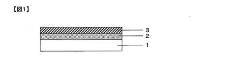
- FIG. 1 is a cross-sectional view showing an example of the gas barrier film of the present invention.
- the gas barrier film of the present invention comprises, on one side of a polymer substrate 1, an inorganic layer [A] containing a zinc compound and silicon oxide from the polymer substrate 1 side, and silicon oxynitride A silicon compound layer [B] containing a product is laminated so as to be in this order.
- the example of FIG. 1 shows the minimum structure of the gas barrier film of the present invention, and only the inorganic layer [A] and the silicon compound layer [B] are arranged on one side of the polymer substrate 1.
- another layer may be disposed between the polymer base material and the inorganic layer [A], and on the side opposite to the side on which the inorganic layer [A] of the polymer base material 1 is laminated.
- Other layers may be arranged.
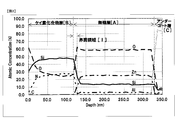
- FIG. 3 shows an example of the gas barrier film of the present invention, in which the surface of the silicon compound layer [B] has a depth (denoted as “Depth” in the figure) of 0.0 nm and is directed toward the inorganic layer [A]. It is the graph which showed the element distribution measured with the X ray photoelectron spectroscopy with respect to the depth.
- the inorganic layer [A] contains zinc, the atomic concentration of zinc (shown as “Atomic Concentration (%)” in the figure) decreases on the side of the silicon compound layer [B].
- the point where the atomic concentration of zinc is minimized is defined as the boundary between the inorganic layer [A] and the silicon compound layer [B].
- the interface region [I] will be described later including the definition.
- the adhesion between the inorganic layer [A] and the silicon compound layer [B] is improved by having a chemical bond between the component constituting the inorganic layer [A] and the component constituting the silicon compound layer [B]. Excellent bending resistance can be obtained.
- the polymer substrate used in the present invention preferably has a film form from the viewpoint of ensuring flexibility.
- the structure of the film may be a single-layer film or a film having two or more layers, for example, a film formed by a coextrusion method.
- a film stretched in a uniaxial direction or a biaxial direction may be used.
- the material of the polymer substrate used in the present invention is not particularly limited, but is preferably an organic polymer as a main constituent.
- organic polymer that can be suitably used in the present invention include crystalline polyolefins such as polyethylene and polypropylene, amorphous cyclic polyolefins having a cyclic structure, polyesters such as polyethylene terephthalate and polyethylene naphthalate, polyamides, polycarbonates, Examples include polystyrene, polyvinyl alcohol, saponified ethylene vinyl acetate copolymer, various polymers such as polyacrylonitrile and polyacetal.
- the organic polymer may be either a homopolymer or a copolymer, and only one type may be used as the organic polymer, or a plurality of types may be blended.
- the surface of the polymer base on which the inorganic layer [A] is formed has a corona treatment, a plasma treatment, an ultraviolet treatment, an ion bombard treatment, a solvent treatment, an organic substance or an inorganic substance to improve adhesion and smoothness.
- a pretreatment such as an undercoat layer forming treatment composed of the above mixture may be applied.
- a coating layer of an organic material, an inorganic material, or a mixture thereof may be laminated for the purpose of improving the slipping property at the time of winding the film.
- the thickness of the polymer substrate used in the present invention is not particularly limited, but is preferably 500 ⁇ m or less from the viewpoint of ensuring flexibility, and preferably 5 ⁇ m or more from the viewpoint of securing strength against tension or impact. Furthermore, the thickness of the polymer substrate is more preferably 10 ⁇ m or more and 200 ⁇ m or less because of the ease of film processing and handling.
- the inorganic layer [A] in the present invention contains a zinc compound and silicon oxide, aluminum (Al), titanium (Ti), zirconium (Zr), tin (Sn), indium (In), niobium (Nb) ), Molybdenum (Mo), tantalum (Ta), or other element oxides, nitrides, sulfides, or mixtures thereof.
- an inorganic layer [A1] composed of a coexisting phase of zinc oxide, silicon dioxide and aluminum oxide or an inorganic layer [A2] composed of a coexisting phase of zinc sulfide and silicon dioxide Preferably used. Details of each of the inorganic layer [A1] and the inorganic layer [A2] will be described later.
- the thickness of the inorganic layer [A] used in the present invention is preferably 10 nm or more and 1,000 nm or less as the thickness of the layer exhibiting gas barrier properties.
- the thickness of the layer is less than 10 nm, there may be a portion where the gas barrier property cannot be sufficiently secured, and the gas barrier property may vary in the polymer substrate surface.
- the thickness of the layer is greater than 1,000 nm, the stress remaining in the layer increases, so that the inorganic layer [A] is liable to crack due to bending or external impact, and the gas barrier properties are increased with use. May decrease.
- the thickness of the inorganic layer [A] is preferably 10 nm or more and 1,000 nm or less, and more preferably 100 nm or more and 500 nm or less from the viewpoint of ensuring flexibility.
- the thickness of the inorganic layer [A] can usually be measured by cross-sectional observation with a transmission electron microscope (TEM).
- the center plane average roughness SRa of the inorganic layer [A] used in the present invention is preferably 10 nm or less.
- SRa is larger than 10 nm, the irregular shape on the surface of the inorganic layer [A] becomes large, and a gap is formed between the sputtered particles to be laminated. The improvement effect may be difficult to obtain.
- SRa is larger than 10 nm, the film quality of the silicon compound layer [B] laminated on the inorganic layer [A] is not uniform, and the gas barrier property may be lowered. Therefore, SRa of the inorganic layer [A] is preferably 10 nm or less, and more preferably 7 nm or less.
- SRa of the inorganic layer [A] in the present invention can be measured using a three-dimensional surface roughness measuring machine.
- the method for forming the inorganic layer [A] is not particularly limited, and can be formed by, for example, a vacuum deposition method, a sputtering method, an ion plating method, a CVD method, or the like.
- the sputtering method is preferable because the inorganic layer [A] can be easily and precisely formed.
- the inorganic layer [A1] which is a layer composed of a coexisting phase of zinc oxide-silicon dioxide-aluminum oxide, which is preferably used as the inorganic layer [A] in the present invention, will be described in detail.
- the “coexisting phase of zinc oxide-silicon dioxide-aluminum oxide” may be abbreviated as “ZnO—SiO 2 —Al 2 O 3 ”.
- silicon (SiO 2) dioxide the generation time of the condition, those slightly deviated from the composition ratio of silicon and oxygen of the left formula but sometimes (SiO ⁇ SiO 2) is produced, silicon dioxide or SiO 2
- SiO 2 the same applies to zinc oxide and aluminum oxide, and zinc oxide or ZnO, aluminum oxide or Al 2 , regardless of the composition ratio deviation depending on the conditions at the time of formation. It shall be written as O 3 .
- the reason why the gas barrier property is improved by applying the inorganic layer [A1] in the gas barrier film of the present invention is that, in the coexisting phase of zinc oxide-silicon dioxide-aluminum oxide, the crystalline component contained in the zinc oxide and the silicon dioxide It is speculated that by coexisting with the amorphous component, the crystal growth of zinc oxide, which tends to produce microcrystals, is suppressed and the particle size is reduced, so that the layer is densified and the permeation of water vapor is suppressed. .
- the coexistence of aluminum oxide can suppress the crystal growth more than the case of coexistence of zinc oxide and silicon dioxide, so that the layer can be further densified, and accordingly, cracks during use can be reduced. It is considered that the gas barrier property deterioration due to the generation could be suppressed.
- the composition of the inorganic layer [A1] can be measured by ICP emission spectroscopy as described later.
- the zinc atom concentration measured by ICP emission spectroscopy is 20 to 40 atom%
- the silicon atom concentration is 5 to 20 atom%
- the aluminum atom concentration is 0.5 to 5 atom%
- the O atom concentration is 35 to 70 atom%.
- the zinc atom concentration is higher than 40 atom% or the silicon atom concentration is lower than 5 atom%, the silicon dioxide and / or aluminum oxide that suppresses the crystal growth of zinc oxide is insufficient, so that void portions and defect portions increase. In some cases, sufficient gas barrier properties cannot be obtained.
- the amorphous component of silicon dioxide inside the layer may increase and the flexibility of the layer may be lowered.
- the aluminum atom concentration is higher than 5 atom%, the affinity between zinc oxide and silicon dioxide becomes excessively high, so that the pencil hardness of the film increases, and cracks are likely to occur due to heat and external stress. is there.
- the aluminum atom concentration is smaller than 0.5 atom%, the affinity between zinc oxide and silicon dioxide becomes insufficient, and the bonding force between the particles forming the layer cannot be improved, so that the flexibility may be lowered.
- the oxygen atom concentration is higher than 70 atom%, the amount of defects in the inorganic layer [A1] increases, so that a desired gas barrier property may not be obtained.
- the oxygen atom concentration is lower than 35 atom%, the oxidation state of zinc, silicon, and aluminum becomes insufficient, the crystal growth cannot be suppressed, and the particle diameter increases, so that the gas barrier property may be lowered.
- the zinc atom concentration is 25 to 35 atom%
- the silicon atom concentration is 10 to 15 atom%
- the aluminum atom concentration is 1 to 3 atom%
- the oxygen atom concentration is 50 to 64 atom%.
- the composition of the inorganic layer [A1] is formed with the same composition as the mixed sintered material used at the time of forming the layer. Therefore, by using a mixed sintered material having a composition that matches the composition of the target layer, the inorganic layer [A1] It is possible to adjust the composition of the layer [A1].
- the composition of the inorganic layer [A1] is calculated as a composition ratio of zinc oxide, silicon dioxide, aluminum oxide, and the inorganic oxide contained by quantifying each element of zinc, silicon, and aluminum by ICP emission spectroscopy.
- the oxygen atoms are calculated on the assumption that zinc atoms, silicon atoms, and aluminum atoms exist as zinc oxide (ZnO), silicon dioxide (SiO 2 ), and aluminum oxide (Al 2 O 3 ), respectively.
- the ICP emission spectroscopic analysis is an analysis method capable of simultaneously measuring multiple elements from an emission spectrum generated when a sample is introduced into a plasma light source unit together with argon gas, and can be applied to composition analysis.
- ICP emission spectroscopic analysis can be performed after removing the layer by ion etching or chemical treatment as necessary.
- the inorganic layer [A2] which is a layer composed of a coexisting phase of zinc sulfide and silicon dioxide, which is preferably used as the inorganic layer [A] in the present invention will be described in detail.
- the “zinc sulfide-silicon dioxide coexisting phase” is sometimes abbreviated as “ZnS—SiO 2 ”.
- silicon dioxide (SiO 2 ) may be generated (SiO to SiO 2 ) slightly deviating from the composition ratio of silicon and oxygen in the composition formula on the left depending on the conditions at the time of production. It shall be written as 2 .
- the deviation of the composition ratio from the chemical formula the same applies to zinc sulfide, and it is expressed as zinc sulfide or ZnS regardless of the deviation of the composition ratio depending on the conditions at the time of production.
- the reason why the gas barrier property is improved by applying the inorganic layer [A2] in the gas barrier film of the present invention is that, in the zinc sulfide-silicon dioxide coexisting phase, the crystalline component contained in the zinc sulfide and the amorphous silicon dioxide It is presumed that by coexisting with the components, crystal growth of zinc sulfide, which is likely to generate microcrystals, is suppressed and the particle diameter is reduced, so that the layer is densified and the permeation of water vapor is suppressed.
- the zinc sulfide-silicon dioxide coexisting phase containing zinc sulfide with suppressed crystal growth is more flexible than a layer formed only of inorganic oxides or metal oxides, and is resistant to heat and external stress.
- the inorganic layer [A2] since it becomes a layer which is hard to generate
- the composition of the inorganic layer [A2] is preferably such that the molar fraction of zinc sulfide relative to the total of zinc sulfide and silicon dioxide is 0.7 to 0.9. If the molar fraction of zinc sulfide with respect to the total of zinc sulfide and silicon dioxide is greater than 0.9, there will be insufficient silicon dioxide to suppress zinc sulfide crystal growth, resulting in an increase in voids and defects, resulting in the prescribed gas barrier properties. May not be obtained.
- the molar fraction of zinc sulfide relative to the total of zinc sulfide and silicon dioxide is less than 0.7, the amorphous component of silicon dioxide inside the inorganic layer [A2] increases and the flexibility of the layer decreases. The flexibility of the gas barrier film against mechanical bending may be reduced.
- a more preferable range of the molar fraction of zinc sulfide relative to the total of zinc sulfide and silicon dioxide is 0.75 to 0.85.
- the composition of the inorganic layer [A2] is formed with the same composition as the mixed sintered material used at the time of forming the layer, by using the mixed sintered material having a composition suitable for the purpose, the inorganic layer [A2] It is possible to adjust the composition.
- the composition ratio of zinc and silicon is first obtained by ICP emission spectroscopic analysis. Based on this value, each element is quantitatively analyzed by using Rutherford backscattering method, and zinc sulfide and silicon dioxide are analyzed. And the composition ratio of other inorganic oxides contained.
- the ICP emission spectroscopic analysis is an analysis method capable of simultaneously measuring multiple elements from an emission spectrum generated when a sample is introduced into a plasma light source unit together with argon gas, and can be applied to composition analysis.
- the inorganic layer [A2] is a composite layer of sulfide and oxide, analysis by Rutherford backscattering method capable of analyzing the composition ratio of sulfur and oxygen is performed.
- the layer is removed by ion etching or chemical treatment as necessary, and then analyzed by ICP emission spectroscopic analysis and Rutherford backscattering method. Can do.
- the silicon compound layer [B] in the present invention is a layer containing silicon oxynitride, and may contain an oxide, a nitride, an organic compound, or a mixture thereof.
- silicon compounds such as SiO 2 , Si 3 N 4 , and alkoxysilane may be included for the purpose of controlling refractive index, hardness, adhesion, and the like.
- the composition of the silicon compound layer [B] can be measured by X-ray photoelectron spectroscopy. From the viewpoint of water vapor permeability, the silicon compound layer [B] preferably contains 0.1 to 100% by mass of silicon oxynitride.
- the silicon compound layer [B] is added to defects such as pinholes and cracks of the inorganic layer [A].
- the silicon oxynitride contained in the metal layer can be filled to exhibit high barrier properties, and the silicon compound layer [B] is in contact with the inorganic layer [A].
- the component such as zinc oxide acts as a catalyst to easily modify the silicon compound layer [B] film quality, and further improve the gas barrier property.
- the inorganic layer [A] and the silicon compound layer [B] Has a chemical bond, the adhesion between the inorganic layer [A] and the silicon compound layer [B] is improved, and it is estimated that excellent bending resistance during use is obtained. Details of the interface region between the inorganic layer [A] and the silicon compound layer [B] will be described later.
- the thickness of the silicon compound layer [B] used in the present invention is preferably from 50 nm to 2,000 nm, more preferably from 50 nm to 1,000 nm. If the thickness of the silicon compound layer [B] is less than 50 nm, stable water vapor barrier performance may not be obtained. When the thickness of the silicon compound layer [B] is greater than 2,000 nm, the residual stress in the silicon compound layer [B] increases, causing the polymer substrate to warp, and the silicon compound layer [B] and / or the inorganic layer A crack may occur in [A] and the gas barrier property may decrease. Therefore, the thickness of the silicon compound layer [B] is preferably 50 nm or more and 2,000 nm or less. The thickness of the silicon compound layer [B] can be measured from a cross-sectional observation image by a transmission electron microscope (TEM).
- TEM transmission electron microscope
- the center surface average roughness SRa of the silicon compound layer [B] used in the present invention is preferably 10 nm or less. It is preferable to set SRa to 10 nm or less because the repeatability of gas barrier properties is improved.
- the SRa on the surface of the silicon compound layer [B] is larger than 10 nm, cracks due to stress concentration are likely to occur in a portion with many irregularities, which may cause a decrease in reproducibility of gas barrier properties. Therefore, in the present invention, the SRa of the silicon compound layer [B] is preferably 10 nm or less, more preferably 7 nm or less.
- SRa of the silicon compound layer [B] in the present invention can be measured using a three-dimensional surface roughness measuring machine.
- the atomic composition ratio of oxygen atoms to silicon atoms is 0.1 or more and less than 2.0, and atoms of nitrogen atoms to silicon atoms The composition ratio is preferably 0.1 or more and less than 1.0.
- the atomic composition ratio of oxygen atoms to silicon atoms is 0.1 or more and less than 2.0, and the atomic composition ratio of nitrogen atoms to silicon atoms is 0.1 or more and less than 1.0.
- a layer having high gas barrier properties and excellent bending resistance is preferably 0.1 or more and less than 1.0.
- the silicon compound layer [B] becomes an excessively dense film. Flexibility is insufficient, cracks are likely to occur due to heat and external stress, and gas barrier properties may be reduced.
- the atomic composition ratio of oxygen atoms to silicon atoms is 2.0 or more, or the atomic composition ratio of nitrogen atoms to silicon atoms is smaller than 0.1, the compactness of the silicon compound layer [B] is insufficient, In some cases, sufficient gas barrier properties cannot be obtained.
- the atomic composition ratio of oxygen atoms to silicon atoms is 0.3 or more and less than 2.0, and the atomic composition ratio of nitrogen atoms to silicon atoms is 0.1 or more and less than 0.8. Is more preferable.
- a silicon compound having a polysilazane skeleton is preferably used as a material of the silicon compound layer [B] used in the present invention.
- the silicon compound having a polysilazane skeleton for example, a compound having a partial structure represented by the following chemical formula (1) can be preferably used.
- one or two or more selected from perhydropolysilazane, organopolysilazane, and derivatives thereof can be used.
- perhydropolysilazane in which all of R 1 , R 2 , and R 3 represented by the following chemical formula (1) are hydrogen from the viewpoint of improving gas barrier properties, but part or all of hydrogen is used. May be an organopolysilazane substituted with an organic group such as an alkyl group.
- the ZnLMM spectrum obtained by X-ray photoelectron spectroscopy in the interface region [I] on the silicon compound layer [B] side of the inorganic layer [A] shows the inorganic layer [A]. It is preferable that it is relatively broad with respect to the same spectrum (for example, shown by a thin line in FIG. 4) in the central portion of the.
- that the ZnLMM spectrum is relatively broad is based on a comparison of the spectrum width at an intensity of 0.4 when the intensity of the peak top is normalized to 1.
- the low binding energy side of the spectrum (the right side of the horizontal axis in FIG. 4 corresponds to the low binding energy side direction) is broad.
- the “interfacial region [I] on the side of the silicon compound layer [B] of the inorganic layer [A]” for measuring the ZnLMM spectrum by X-ray photoelectron spectroscopy is the silicon compound layer [ B] is a region where nitrogen atoms and zinc atoms coexist when the element distribution is measured in the depth direction from the surface of B] by the X-ray photoelectron spectroscopy, and the central portion of the inorganic layer [A] is the silicon compound layer
- the depth position is half the total depth of the inorganic layer [A]. This means a region of ⁇ 20 nm.
- the interface region [I] contains a relatively large amount of a Zn compound having a bonding state different from that of ZnO as compared with the central portion of the inorganic layer [A].
- the composition of the inorganic layer [A] and the silicon compound layer [B] and the interface region [I] contains a relatively large amount of Zn compound in a bonded state different from ZnO.
- [I] is considered to be a region formed by the reaction of a mixture of the inorganic layer [A] and the silicon compound layer [B].
- the silicon layer has defects such as pinholes and cracks in the inorganic layer [A]. It is considered that the compound layer [B] is filled and a chemical bond is formed, and this makes it possible to develop a high barrier property. In addition, it is considered that the adhesion between the inorganic layer [A] and the silicon compound layer [B] is improved, and excellent bending resistance can be obtained.
- a polyurethane compound [C1] having an aromatic ring structure is crosslinked between the polymer substrate and the inorganic layer [A] in order to improve gas barrier properties and flex resistance. It is preferable to provide an undercoat layer [C] containing a structure obtained in this manner. When defects such as protrusions and small scratches are present on the polymer substrate, pinholes and cracks also occur in the inorganic layer [A] laminated on the polymer substrate starting from the defects, resulting in gas barrier properties and resistance. Since the flexibility may be impaired, it is preferable to provide the undercoat layer [C] of the present invention.
- the undercoat layer [C] used in the present invention preferably contains a polyurethane compound [C1] having an aromatic ring structure from the viewpoints of thermal dimensional stability and flex resistance, and is further ethylenically unsaturated. It is more preferable that the compound [C2], the photopolymerization initiator [C3], the organosilicon compound [C4] and / or the inorganic silicon compound [C5] is contained.
- the polyurethane compound [C1] having an aromatic ring structure used in the present invention has an aromatic ring and a urethane bond in the main chain or side chain, for example, an epoxy having a hydroxyl group and an aromatic ring in the molecule. It can be obtained by polymerizing (meth) acrylate (c1), diol compound (c2), and diisocyanate compound (c3).
- Examples of the epoxy (meth) acrylate (c1) having a hydroxyl group and an aromatic ring in the molecule include aromatic glycols such as bisphenol A type, hydrogenated bisphenol A type, bisphenol F type, hydrogenated bisphenol F type, resorcin, and hydroquinone. This can be obtained by reacting the diepoxy compound with a (meth) acrylic acid derivative.
- diol compound (c2) examples include ethylene glycol, diethylene glycol, polyethylene glycol, propylene glycol, 1,3-propanediol, 1,3-butanediol, 1,4-butanediol, 1,5-pentanediol, , 6-hexanediol, 1,7-heptanediol, 1,8-octanediol, 1,9-nonanediol, 1,10-decanediol, 2,4-dimethyl-2-ethylhexane-1,3-diol Neopentyl glycol, 2-ethyl-2-butyl-1,3-propanediol, 3-methyl-1,5-pentanediol, 1,2-cyclohexanedimethanol, 1,4-cyclohexanedimethanol, 2,2 , 4,4-Tetramethyl-1,3-cyclobutanediol,
- diisocyanate compound (c3) examples include 1,3-phenylene diisocyanate, 1,4-phenylene diisocyanate, 2,4-tolylene diisocyanate, 2,6-tolylene diisocyanate, 2,4-diphenylmethane diisocyanate, 4,4.
- -Aromatic diisocyanates such as diphenylmethane diisocyanate, aliphatic diisocyanates such as ethylene diisocyanate, hexamethylene diisocyanate, 2,2,4-trimethylhexamethylene diisocyanate, 2,4,4-trimethylhexamethylene diisocyanate, lysine diisocyanate, lysine triisocyanate
- Diisocyanate compounds isophorone diisocyanate, dicyclohexylmethane-4,4-diisocyanate, methylcyclohexylene diisocyanate
- Alicyclic isocyanate compounds such as xylylene diisocyanate, aromatic aliphatic isocyanate compounds such as tetramethyl xylylene diisocyanate. These can be used alone or in combination of two or more.
- the component ratios of (c1), (c2), and (c3) are not particularly limited as long as they are within a desired weight average molecular weight.
- the polyurethane compound [C1] having an aromatic ring structure of the present invention preferably has a weight average molecular weight (Mw) of 5,000 to 100,000.
- a weight average molecular weight (Mw) of 5,000 to 100,000 is preferable because the resulting cured film has excellent thermal dimensional stability and flex resistance.
- the weight average molecular weight (Mw) of this invention is the value measured using the gel permeation chromatography method and converted with standard polystyrene.
- Examples of the ethylenically unsaturated compound [C2] include di (meth) acrylates such as 1,4-butanediol di (meth) acrylate and 1,6-hexanediol di (meth) acrylate, and pentaerythritol tri (meth).
- Polyfunctional (meth) acrylates such as acrylate, pentaerythritol tetra (meth) acrylate, dipentaerythritol tetra (meth) acrylate, dipentaerythritol penta (meth) acrylate, dipentaerythritol hexa (meth) acrylate, bisphenol A type epoxy di ( Examples thereof include epoxy acrylates such as (meth) acrylate, bisphenol F type epoxy di (meth) acrylate, and bisphenol S type epoxy di (meth) acrylate. Among these, polyfunctional (meth) acrylates excellent in thermal dimensional stability and surface protection performance are preferable. Moreover, these may be used by a single composition, and may mix and use two or more components.
- the content of the ethylenically unsaturated compound [C2] is not particularly limited, but from the viewpoint of thermal dimensional stability and surface protection performance, the total amount with the polyurethane compound [C1] having an aromatic ring structure is 100% by mass. It is preferably in the range of -90% by mass, more preferably in the range of 10-80% by mass.
- the material for the photopolymerization initiator [C3] is not particularly limited as long as the gas barrier property and the bending resistance of the gas barrier film of the present invention can be maintained.
- Examples of the photopolymerization initiator that can be suitably used in the present invention include 2,2-dimethoxy-1,2-diphenylethane-1-one, 1-hydroxy-cyclohexylphenyl-ketone, 2-hydroxy-2- Methyl-1-phenyl-propan-1-one, 1- [4- (2-hydroxyethoxy) -phenyl] -2-hydroxy-2-methyl-1-propan-1-one, 2-hydroxy-1- ⁇ 4- [4- (2-hydroxy-2-methyl-propionyl) -benzyl] phenyl ⁇ -2-methyl-propan-1-one, phenylglyoxylic acid methyl ester, 2-methyl-1- (4-methylthio Phenyl) -2-morpholinopropan-1-one, 2-benzyl-2-di
- a photopolymerization initiator selected from -trimethylbenzoyl-diphenyl-phosphine oxide and bis (2,4,6-trimethylbenzoyl) -phenylphosphine oxide is preferred.
- these may be used by a single composition, and may mix and use two or more components.
- the content of the photopolymerization initiator [C3] is not particularly limited, but from the viewpoint of curability and surface protection performance, it may be in the range of 0.01 to 10% by mass in 100% by mass of the total amount of polymerizable components. The range is preferably from 0.1 to 5% by mass.
- Organosilicon compound [C4] examples include vinyltrimethoxysilane, vinyltriethoxysilane, 2- (3,4-epoxycyclohexyl) ethyltrimethoxysilane, 3-glycidoxypropylmethyldimethoxysilane, and 3-glycidide.
- Organosilicon compounds are preferred. Moreover, these may be used by a single composition, and may mix and use two or more components.
- the content of the organosilicon compound [C4] is not particularly limited, but is preferably in the range of 0.01 to 10% by mass in 100% by mass of the total amount of polymerizable components from the viewpoint of curability and surface protection performance.
- the range of 0.1 to 5% by mass is more preferable.
- silica particles are preferable from the viewpoint of surface protection performance and transparency, and the primary particle diameter of the silica particles is preferably in the range of 1 to 300 nm, and preferably in the range of 5 to 80 nm. Is more preferable.
- the primary particle diameter here refers to the particle diameter d calculated
- the thickness of the undercoat layer [C] is preferably 200 nm or more and 4,000 nm or less. If the thickness of the undercoat layer [C] is less than 200 nm, the adverse effects of defects such as protrusions and small scratches present on the polymer substrate may not be suppressed. When the thickness of the undercoat layer [C] becomes thicker than 4,000 nm, the smoothness of the undercoat layer [C] is lowered, and the uneven shape on the surface of the inorganic layer [A] laminated on the undercoat layer [C] is also reduced.
- the thickness of the undercoat layer [C] is preferably 200 nm or more and 4,000 nm or less.
- the thickness of the silicon compound layer [B] can be measured from a cross-sectional observation image by a transmission electron microscope (TEM).
- the center surface average roughness SRa of the undercoat layer [C] is preferably 10 nm or less. SRa of 10 nm or less is preferable because a homogeneous inorganic layer [A] can be easily obtained on the undercoat layer [C], and the reproducibility of gas barrier properties is improved.
- the SRa on the surface of the undercoat layer [C] is larger than 10 nm, the uneven shape on the surface of the inorganic layer [A] on the undercoat layer [C] also becomes large, and a gap is formed between the sputtered particles to be laminated.
- the SRa of the undercoat layer [C] is preferably 10 nm or less, more preferably 7 nm or less.
- SRa of the undercoat layer [C] in the present invention can be measured using a three-dimensional surface roughness measuring machine.
- a hard coat layer may be formed for the purpose of improving scratch resistance as long as the gas barrier property does not deteriorate, or a film made of an organic polymer compound is laminated. It is good also as a laminated structure.
- the outermost surface as used herein refers to the side that is not in contact with the inorganic layer [A] after being laminated in this order so that the inorganic layer [A] and the silicon compound layer [B] are in contact with each other on the polymer substrate. The surface of the silicon compound layer [B].
- the gas barrier film of the present invention comprises a step a in which an inorganic layer [A] containing a zinc compound and a silicon oxide is formed on a polymer substrate by a sputtering method, and a polysilazane skeleton is formed on the inorganic layer [A].
- a coating liquid containing a silicon compound having a coating is formed and dried to form a coating film, and then the coating film is subjected to an active energy ray irradiation treatment in a nitrogen atmosphere to provide a silicon compound layer [B] containing silicon oxynitride It is produced through a process including the process b.
- the gas barrier film of the present invention is formed by applying a coating liquid containing a polyurethane compound [C1] having an aromatic ring structure on a polymer base material, followed by drying to form a coating film.
- a coating liquid containing a silicon compound having a polysilazane skeleton is applied on the inorganic layer [A] and dried to form a coating film, and then the coating film is irradiated with active energy rays in a nitrogen atmosphere It is manufactured through a process including a process b in which a silicon compound layer [B] containing silicon oxide and silicon oxynitride is processed.
- step a since an inorganic layer can be formed easily and precisely, it is preferable to use a winding type sputtering apparatus having a structure shown in FIG. Since the composition of the inorganic layer [A] is formed with the same composition as the mixed sintered material used at the time of forming the layer, the composition can be obtained by using a mixed sintered material having a composition that matches the composition of the target layer. Can be adjusted.
- a winding-type sputtering apparatus in which a sputtering target sintered with a composition of zinc oxide / silicon dioxide / aluminum oxide is installed on the sputtering electrode may be used. Furthermore, it is preferable to use a sputter target sintered at a composition mass ratio of zinc oxide / silicon dioxide / aluminum oxide of 77/20/3.
- the polymer substrate is set on the winding roll so that the surface on which the inorganic layer [A1] is provided faces the sputtering electrode, Unwind and pass through the cooling drum through the guide roll.
- Argon gas and oxygen gas were introduced at an oxygen gas partial pressure of 10% so that the degree of decompression was 2 ⁇ 10 ⁇ 1 Pa, and argon / oxygen gas plasma was generated by applying an input power of 4,000 W from a DC power source.
- the inorganic layer [A1] is formed on the surface of the polymer substrate by sputtering. The thickness is adjusted to a desired thickness depending on the film conveyance speed. Then, it winds up on a winding roll via a guide roll.
- a roll-up type sputtering apparatus in which a sputtering target sintered with a composition of zinc sulfide / silicon dioxide is installed on the sputtering electrode may be used. Furthermore, it is preferable to use a sputter target sintered at a zinc sulfide / silicon dioxide molar ratio of 80/20.
- the polymer substrate is set on the take-up roll so that the surface on which the inorganic layer [A2] is provided faces the sputter electrode, Unwind and pass through the cooling drum through the guide roll.
- Argon gas was introduced so that the degree of decompression was 2 ⁇ 10 ⁇ 1 Pa, and by applying an input power of 500 W from a high frequency power source, argon plasma was generated, and an inorganic layer [on the surface of the polymer substrate by sputtering [ A2] is formed.
- the thickness is adjusted to a desired thickness depending on the film conveyance speed. Then, it winds up on a winding roll via a guide roll.
- the undercoat layer [C] is formed on the polymer substrate prior to step a. ] May be formed on the undercoat layer [C] in the same manner to form the inorganic layer [A].
- the method for forming the undercoat layer [C] will be described in the description of step c.
- step b first, the solid content concentration is adjusted so that the thickness after drying of the coating containing a silicon compound having a polysilazane skeleton on the inorganic layer [A] becomes a desired thickness, and the reverse coating method, gravure coating method, rod coating method. It is preferably applied by a bar coating method, a die coating method, a spray coating method, a spin coating method, or the like.
- the silicon compound having a polysilazane skeleton one or a combination of two or more selected from perhydropolysilazane, organopolysilazane, and derivatives thereof can be used.
- a paint containing a silicon compound layer having a polysilazane skeleton using an organic solvent from the viewpoint of coating suitability.
- an organic solvent such as xylene, toluene, methylcyclohexane, pentane or hexane, or an ether solvent such as dibutyl ether, ethyl butyl ether or tetrahydrofuran
- the solid content concentration is diluted to within 10% by mass.
- solvents may be used alone or in combination of two or more.
- Various additives can be blended in the coating material containing the silicon compound forming the silicon compound layer [B], if necessary, as long as the effect of the silicon compound layer [B] is not impaired.
- a catalyst an antioxidant, a light stabilizer, a stabilizer such as an ultraviolet absorber, a surfactant, a leveling agent, an antistatic agent, or the like can be used.
- the heating temperature is preferably 50 to 150 ° C.
- the heat treatment time is preferably several seconds to 1 hour.
- the temperature may be constant during the heat treatment, or the temperature may be gradually changed.
- the heat treatment may be performed while adjusting the humidity within the range of 20 to 90% RH in terms of relative humidity. You may perform the said heat processing in the state enclosed with air
- the coating film containing a silicon compound having a polysilazane skeleton after drying is subjected to active energy ray irradiation treatment such as plasma treatment, ultraviolet irradiation treatment, flash pulse treatment, etc. to modify the composition of the coating film, and silicon oxynitriding
- active energy ray irradiation treatment such as plasma treatment, ultraviolet irradiation treatment, flash pulse treatment, etc.
- the composition of the silicon compound layer [B] measured by X-ray photoelectron spectroscopy can be controlled by the amount of irradiation with active energy rays, and the atomic composition ratio of oxygen atoms to silicon atoms is 0.1 or more and 2.0. And an atomic composition ratio of nitrogen atoms to silicon atoms is adjusted to be 0.1 or more and less than 1.0.
- the active energy ray irradiation treatment in step b it is preferable to use an ultraviolet treatment because it is simple and excellent in productivity, and it is easy to obtain a uniform silicon compound layer [B] composition.
- the ultraviolet treatment may be performed under atmospheric pressure or reduced pressure, but in the present invention, the ultraviolet treatment is preferably performed under atmospheric pressure from the viewpoint of versatility and production efficiency.
- the oxygen gas partial pressure is preferably 1.0% or less, and more preferably 0.5% or less.
- the relative humidity may be arbitrary. In the ultraviolet treatment, it is more preferable to reduce the oxygen concentration using nitrogen gas.
- the ultraviolet ray generation source a known source such as a high pressure mercury lamp metal halide lamp, a microwave type electrodeless lamp, a low pressure mercury lamp, a xenon lamp, or the like can be used.
- the accumulated amount of ultraviolet irradiation is preferably 0.5 to 10 J / cm 2 , more preferably 0.8 to 7 J / cm 2 . If the integrated light quantity is 0.5 J / cm 2 or more, a desired silicon compound layer [B] composition can be obtained, which is preferable. Moreover, it is preferable if the integrated light quantity is 10 J / cm 2 or less because damage to the polymer substrate and the inorganic layer [B] can be reduced.
- the heating temperature is preferably 50 to 150 ° C, more preferably 80 to 130 ° C.
- a heating temperature of 50 ° C. or higher is preferable because high production efficiency can be obtained, and a heating temperature of 150 ° C. or lower is preferable because deformation and alteration of other materials such as a polymer base material hardly occur.
- an undercoat layer [C] can be provided by the process c as needed.
- step c first, the solid content concentration is adjusted so that the thickness after drying of the coating material containing the polyurethane compound [C1] having an aromatic ring structure on the polymer substrate becomes a desired thickness. It is preferable to apply by a coating method, a rod coating method, a bar coating method, a die coating method, a spray coating method, a spin coating method or the like. Moreover, in this invention, it is preferable to dilute the coating material containing the polyurethane compound [C1] which has an aromatic ring structure using an organic solvent from a viewpoint of coating suitability.
- the solid content concentration is diluted to within 10% by mass.
- a hydrocarbon solvent such as xylene, toluene, methylcyclohexane, pentane or hexane, or an ether solvent such as dibutyl ether, ethyl butyl ether or tetrahydrofuran
- these solvents may be used alone or in combination of two or more.
- various additives can be mix
- a catalyst, an antioxidant, a light stabilizer, a stabilizer such as an ultraviolet absorber, a surfactant, a leveling agent, an antistatic agent, or the like can be used.
- the heating temperature is preferably 50 to 150 ° C.
- the heat treatment time is preferably several seconds to 1 hour.
- the temperature may be constant during the heat treatment, or the temperature may be gradually changed.
- the heat treatment may be performed while adjusting the humidity within the range of 20 to 90% RH in terms of relative humidity. The heat treatment may be performed in the air or while enclosing an inert gas.
- an undercoat layer [C] by subjecting the coating film containing the polyurethane compound [C1] having an aromatic ring structure after drying to an active energy ray irradiation treatment to crosslink the coating film.
- the active energy ray applied in such a case is not particularly limited as long as the undercoat layer [C] can be cured, but it is preferable to use ultraviolet treatment from the viewpoint of versatility and efficiency.
- the ultraviolet ray generation source a known source such as a high pressure mercury lamp metal halide lamp, a microwave type electrodeless lamp, a low pressure mercury lamp, a xenon lamp or the like can be used.
- an active energy ray in inert gas atmosphere, such as nitrogen and argon from a viewpoint of hardening efficiency.
- the ultraviolet treatment may be performed under atmospheric pressure or reduced pressure, but in the present invention, the ultraviolet treatment is preferably performed under atmospheric pressure from the viewpoint of versatility and production efficiency.
- the oxygen concentration during the ultraviolet treatment is preferably 1.0% or less, more preferably 0.5% or less.
- the relative humidity may be arbitrary.
- the ultraviolet ray generation source a known source such as a high pressure mercury lamp metal halide lamp, a microwave type electrodeless lamp, a low pressure mercury lamp, a xenon lamp, or the like can be used.
- Integrated light quantity of ultraviolet irradiation is preferably from 0.1 ⁇ 1.0J / cm 2, more preferably 0.2 ⁇ 0.6J / cm 2. It is preferable that the integrated light amount is 0.1 J / cm 2 or more because a desired degree of crosslinking of the undercoat layer [C] can be obtained. Moreover, it is preferable if the integrated light quantity is 1.0 J / cm 2 or less because damage to the polymer substrate can be reduced.
- the electronic device of the present invention Since the electronic device of the present invention has the gas barrier film of the present invention, the electronic device of the present invention has an excellent gas barrier property, and can suppress deterioration in the performance of the device due to water vapor or the like.
- Layer thickness Samples for cross-sectional observation are obtained by the FIB method using a microsampling system (FB-2000A, manufactured by Hitachi, Ltd.) (specifically, “Surfacework on Polymer Surfaces” (by Atsushi Iwamori) p 119-119)).
- FB-2000A microsampling system
- H-9000UHRII transmission electron microscope
- composition analysis of [A1] was performed by ICP emission spectroscopic analysis (manufactured by SII Nanotechnology, SPS4000).
- the sample sampled at the stage of forming the inorganic layer [A1] on the polymer substrate (before the silicon compound layer [B] was laminated) was thermally decomposed with nitric acid and sulfuric acid, heated and dissolved with dilute nitric acid, and filtered.
- the insoluble matter was ashed by heating, melted with sodium carbonate, dissolved with dilute nitric acid, and made up to a constant volume with the previous filtrate.
- composition of inorganic layer [A2] was performed by ICP emission spectroscopic analysis (SPS4000, manufactured by SII Nanotechnology).
- SPS4000 ICP emission spectroscopic analysis
- the sample sampled at the stage where the inorganic layer [A2] was formed on the polymer substrate (before the silicon compound layer [B] was laminated) was thermally decomposed with nitric acid and sulfuric acid, heated and dissolved with dilute nitric acid, and filtered. .
- the insoluble matter was incinerated by heating, melted with sodium carbonate, dissolved with dilute nitric acid, and made up to a constant volume with the previous filtrate. About this solution, content of a zinc atom and a silicon atom was measured.
- the Rutherford backscattering method (AN-2500 manufactured by Nissin High Voltage Co., Ltd.) was used to quantitatively analyze zinc atoms, silicon atoms, sulfur atoms, and oxygen atoms. And the composition ratio of silicon dioxide.
- composition of silicon compound layer [B] and confirmation of presence / absence of interface region [I] Using X-ray photoelectron spectroscopy (XPS method), composition in the depth direction for carbon, nitrogen, oxygen, aluminum, silicon, and zinc Analysis was performed to obtain an element distribution as shown in FIG.
- the atomic composition ratio of oxygen atoms to silicon atoms and the atomic composition ratio of nitrogen atoms to silicon atoms at each depth were calculated, and the maximum value and the minimum value were obtained.
- the presence or absence of the interface region [I] was also confirmed when calculating the composition ratio.
- the measurement conditions were as follows.
- Quantera SXM Quantera SXM
- Excitation X-ray monochromatic Al K ⁇ 1,2 line (1486.6 eV)
- X-ray diameter 100 ⁇ m
- Ion etching Ar + ion 2 kV
- Raster size 2 ⁇ 2 mm.
- the specific operation is as follows. First, in a winding roll of a winding-type sputtering apparatus in which a sputtering target sintered with a composition mass ratio of zinc oxide / silicon dioxide / aluminum oxide of 77/20/3 is installed on a sputtering electrode, The polymer substrate was set so that the surface on which the inorganic layer [A1] is provided faces the sputter electrode, unwound, and passed through a cooling drum via a guide roll. Argon gas and oxygen gas were introduced at an oxygen gas partial pressure of 10% so that the degree of decompression was 2 ⁇ 10 ⁇ 1 Pa, and an argon / oxygen gas plasma was generated by applying an input power of 4000 W from a direct current power source. Thus, an inorganic layer [A1] was formed on the surface of the polymer substrate. The thickness was adjusted by the film transport speed. Then, it wound up on the winding roll via the guide roll.
- An inorganic layer is formed by using a winding type sputtering apparatus having a structure shown in FIG. 2 and performing sputtering using a sputter target which is a mixed sintered material formed of zinc sulfide and silicon dioxide on one side of a polymer base material. [A2] was provided.
- the specific operation is as follows. First, in the winding chamber of a winding-type sputtering apparatus in which a sputtering target sintered with a zinc sulfide / silicon dioxide molar composition ratio of 80/20 is installed on a sputtering electrode, the polymer substrate is placed on a winding roll. Was set, unwound, and passed through a cooling drum through a guide roll. Argon gas was introduced so that the degree of decompression was 2 ⁇ 10 ⁇ 1 Pa, and an argon gas plasma was generated by applying an input power of 500 W from a high frequency power source, and an inorganic layer was formed on the surface of the polymer substrate by sputtering. [A2] was formed. The thickness was adjusted by the film transport speed. Then, it wound up on the winding roll via the guide roll.
- Example 1 A polyethylene terephthalate film (“Lumirror” (registered trademark) U48 manufactured by Toray Industries, Inc.) having a thickness of 50 ⁇ m was used as the polymer substrate, and the inorganic layer [A1] was provided on one side of the polymer substrate so as to have a thickness of 180 nm. .
- the Zn atom concentration was 27.5 atom%
- the Si atom concentration was 13.1 atom%
- the Al atom concentration was 2.3 atom%
- the O atom concentration was 57.1 atom%.
- a test piece having a length of 100 mm and a width of 100 mm was cut out from the film on which the inorganic layer [A1] was formed, and the center plane average roughness SRa of the inorganic layer [A1] was evaluated.
- the results are shown in Table 1.
- a coating liquid for forming the silicon compound layer [B] a coating agent containing perhydropolysilazane as a main component and a palladium catalyst (“NL120-20” manufactured by AZ Electronic Materials, solid content concentration: 20 parts by mass)
- a coating liquid 1 is prepared by diluting 100 parts by mass with 300 parts by mass of dibutyl ether, and the coating liquid 1 is applied on the inorganic layer [A1] with a micro gravure coater (gravure wire number 200UR, gravure rotation ratio 100%), 120 ° C. Was dried for 1 minute, and after drying, an ultraviolet treatment was performed under the following conditions to provide a silicon compound layer [B] having a thickness of 120 nm to obtain a gas barrier film.
- a micro gravure coater gravure wire number 200UR, gravure rotation ratio 100%
- Ultraviolet treatment device MEIRH-M-1-152-H (manufactured by M. D. Excimer) Introduced gas: N 2 Integrated light quantity: 3,000 mJ / cm 2 Sample temperature control: 100 ° C
- the obtained gas barrier film was subjected to composition analysis using X-ray photoelectron spectroscopy (XPS method) to determine the element distribution in the depth direction.
- XPS method X-ray photoelectron spectroscopy
- Example 2 A polyethylene terephthalate film (“Lumirror” (registered trademark) U48 manufactured by Toray Industries, Inc.) having a thickness of 50 ⁇ m was used as the polymer substrate.
- a coating liquid for forming the undercoat layer [C] 150 parts by mass of the polyurethane compound, 20 parts by mass of dipentaerythritol hexaacrylate (manufactured by Kyoeisha Chemical Co., Ltd., trade name: Light Acrylate DPE-6A), and 1-hydroxy- 5 parts by mass of cyclohexyl phenyl-ketone (manufactured by BASF Japan, trade name: IRGACURE 184), 3 parts by mass of 3-methacryloxypropylmethyldiethoxysilane (manufactured by Shin-Etsu Silicone, trade name: KBM-503), and ethyl acetate 170 parts by mass of toluene, 350 parts by mass of toluene, and 1
- the coating liquid 2 is applied onto the polymer substrate with a micro gravure coater (gravure wire number 150UR, gravure rotation ratio 100%), dried at 100 ° C. for 1 minute, dried, and then subjected to UV treatment under the following conditions.
- An undercoat layer [C] having a thickness of 1,000 nm was provided.
- Ultraviolet treatment device LH10-10Q-G (manufactured by Fusion UV Systems Japan) Introduced gas: N 2 (nitrogen inert BOX) Ultraviolet light source: Microwave type electrodeless lamp Integrated light quantity: 400 mJ / cm 2 Sample temperature control: room temperature.
- an inorganic layer [A1] was provided on the undercoat layer [C] so as to have a thickness of 180 nm.
- the Zn atom concentration was 27.5 atom%
- the Si atom concentration was 13.1 atom%
- the Al atom concentration was 2.3 atom%
- the O atom concentration was 57.1 atom%.
- a test piece having a length of 100 mm and a width of 100 mm was cut out from the film on which the inorganic layer [A1] was formed, and the center plane average roughness SRa of the inorganic layer [A1] was evaluated. The results are shown in Table 1.
- a coating liquid for forming the silicon compound layer [B] a coating agent containing perhydropolysilazane as a main component and a palladium catalyst (“NL120-20” manufactured by AZ Electronic Materials, solid content concentration: 20 parts by mass)
- a coating liquid 1 was prepared by diluting 100 parts by mass with 300 parts by mass of dibutyl ether.
- the coating liquid 1 is applied onto the inorganic layer [A1] with a micro gravure coater (gravure wire number 200UR, gravure rotation ratio 100%), dried at 120 ° C. for 1 minute, and then subjected to ultraviolet treatment under the following conditions.
- a silicon compound layer [B] having a thickness of 120 nm was provided to obtain a gas barrier film.
- Ultraviolet treatment device MEIRH-M-1-152-H (manufactured by M. D. Excimer) Introduced gas: N 2 Ultraviolet light source: excimer lamp (172 nm) Integrated light quantity: 3,000 mJ / cm 2 Sample temperature control: 100 ° C A test piece having a length of 100 mm and a width of 140 mm was cut out from the obtained gas barrier film, and the water vapor permeability was evaluated. The results are shown in Table 1.
- Example 3 A gas barrier film was obtained in the same manner as in Example 1 except that an amorphous cyclic polyolefin film having a thickness of 100 ⁇ m (“Zeonor Film” ZF14 manufactured by Nippon Zeon Co., Ltd.) was used as the polymer substrate.
- an amorphous cyclic polyolefin film having a thickness of 100 ⁇ m (“Zeonor Film” ZF14 manufactured by Nippon Zeon Co., Ltd.) was used as the polymer substrate.
- Example 4 A gas barrier film was obtained in the same manner as in Example 2 except that an amorphous cyclic polyolefin film having a thickness of 100 ⁇ m (“ZEONOR FILM” ZF14 manufactured by Nippon Zeon Co., Ltd.) was used as the polymer substrate.
- an amorphous cyclic polyolefin film having a thickness of 100 ⁇ m (“ZEONOR FILM” ZF14 manufactured by Nippon Zeon Co., Ltd.) was used as the polymer substrate.
- Example 5 A gas barrier film was obtained in the same manner as in Example 2 except that the inorganic layer [A1] was provided to have a thickness of 950 nm.
- Example 6 A gas barrier film was obtained in the same manner as in Example 2 except that the inorganic layer [A2] was provided to a thickness of 150 nm in place of the inorganic layer [A1].
- Example 7 A gas barrier film was obtained in the same manner as in Example 2 except that the silicon compound layer [B] was provided to have a thickness of 50 nm.
- Example 8 A gas barrier film was obtained in the same manner as in Example 2 except that the silicon compound layer [B] was provided to have a thickness of 1,000 nm.
- Example 9 The gas barrier was applied in the same manner as in Example 2 except that the coating for the silicon compound layer [B] was applied and dried, and then the silicon compound layer [B] was formed by treatment at 80 ° C. for 3 days in a nitrogen atmosphere instead of the ultraviolet treatment. A characteristic film was obtained.
- Example 10 As a coating for the silicon compound layer [B], 100 parts by mass of a coating agent (“NAX120-20” manufactured by AZ Electronic Materials Co., Ltd., solid content concentration 20 parts by mass) containing perhydropolysilazane as a main component and an amine catalyst A gas barrier film was obtained in the same manner as in Example 2 except that the coating liquid diluted with 300 parts by mass of butyl ether was used.
- a coating agent (“NAX120-20” manufactured by AZ Electronic Materials Co., Ltd., solid content concentration 20 parts by mass) containing perhydropolysilazane as a main component and an amine catalyst
- Example 11 As a coating for the silicon compound layer [B], 100 parts by mass of a coating agent (“NN120-20” manufactured by AZ Electronic Materials, solid content concentration of 20 parts by mass) containing perhydropolysilazane as a main component and containing no catalyst is dibutyl ether. A gas barrier film was obtained in the same manner as in Example 2 except that the coating liquid diluted with 300 parts by mass was used.
- a coating agent (“NN120-20” manufactured by AZ Electronic Materials, solid content concentration of 20 parts by mass) containing perhydropolysilazane as a main component and containing no catalyst is dibutyl ether.
- a gas barrier film was obtained in the same manner as in Example 2 except that the coating liquid diluted with 300 parts by mass was used.
- Example 1 Comparative Example 1 Except that the inorganic layer [A] was not formed on the polymer substrate, and the silicon compound layer [B] was provided directly on the surface of the polymer substrate so as to have a thickness of 120 nm, the same as in Example 1. A gas barrier film was obtained.
- Example 2 A gas barrier film was obtained in the same manner as in Example 1 except that the silicon compound layer [B] was not provided on the inorganic layer [A].
- Example 3 (Comparative Example 3) In Example 1, the order of forming the inorganic layer [A] and the silicon compound layer [B] was changed to obtain a gas barrier film having a layer configuration different from that of Example 1.
- the gas barrier film of the present invention is excellent in gas barrier properties against oxygen gas, water vapor, etc., it can be usefully used, for example, as a packaging material for foods, pharmaceuticals, etc., and as a member for electronic devices such as thin televisions and solar cells.
- the application is not limited to these.
Abstract
Description
(1)高分子基材の少なくとも片側に、無機層[A]と、ケイ素化合物層[B]とを前記高分子基材側からこの順に有するガスバリア性フィルムであって、無機層[A]が、亜鉛化合物とケイ素酸化物とを含み、ケイ素化合物層[B]が、ケイ素酸窒化物を含み、かつ無機層[A]とケイ素化合物層[B]が接しているガスバリア性フィルム。
(2)前記高分子基材と前記無機層[A]との間に、芳香族環構造を有するポリウレタン化合物[C1]を架橋して得られる構造を含むアンダーコート層[C]を有する(1)に記載のガスバリア性フィルム。
(3)前記無機層[A]が、酸化亜鉛と二酸化ケイ素と酸化アルミニウムの共存相からなる無機層[A1]または硫化亜鉛と二酸化ケイ素の共存相からなる無機層[A2]のいずれかである(1)または(2)に記載のガスバリア性フィルム。
(4)前記無機層[A]が前記無機層[A1]であり、該無機層[A1]が、ICP発光分光分析法により測定される亜鉛原子濃度が20~40atom%、ケイ素原子濃度が5~20atom%、アルミニウム原子濃度が0.5~5atom%、酸素原子濃度が35~70atom%である組成により構成されたものである(3)に記載のガスバリア性フィルム。
(5)前記無機層[A]が前記無機層[A2]であり、該無機層[A2]は、硫化亜鉛と二酸化ケイ素の合計に対する硫化亜鉛のモル分率が0.7~0.9である組成により構成されたものである(3)に記載のガスバリア性フィルム。
(6)前記ケイ素化合物層[B]が、X線光電子分光法で元素分布を測定した際に、ケイ素原子に対する酸素原子の原子組成比が0.1以上、2.0未満、かつケイ素原子に対する窒素原子の原子組成比が0.1以上、1.0未満である(1)~(5)のいずれかに記載のガスバリア性フィルム。
(7)前記アンダーコート層[C]が有機ケイ素化合物および/または無機ケイ素化合物を含む(2)~(6)のいずれかに記載のガスバリア性フィルム。
(8)(1)~(7)のいずれかに記載のガスバリア性フィルムを有する電子デバイス。
(9)高分子基材上に、スパッタリング法により亜鉛化合物とケイ素酸化物とを含む無機層[A]を設ける工程aと、該無機層[A]上に、ポリシラザン骨格を持つケイ素化合物を含む塗液を塗布後乾燥させて塗膜を形成し、次いで該塗膜に窒素雰囲気下で活性エネルギー線照射処理をしてケイ素酸窒化物を含むケイ素化合物層[B]を設ける工程bとを含むガスバリア性フィルムの製造方法。
(10)高分子基材上に、芳香族環構造を有するポリウレタン化合物[C1]を含む塗液を塗布後乾燥させて塗膜を形成し、次いで該塗膜に窒素雰囲気下で活性エネルギー線照射処理をしてアンダーコート層[C]を設ける工程cと、該アンダーコート層[C]上に、スパッタリング法により亜鉛化合物とケイ素酸化物とを含む無機層[A]を設ける工程aと、該無機層[A]上に、ポリシラザン骨格を持つケイ素化合物を含む塗液を塗布後乾燥させて塗膜を形成し、次いで該塗膜に窒素雰囲気下で活性エネルギー線照射処理をしてケイ素酸化物とケイ素酸窒化物とを含むケイ素化合物層[B]を設ける工程bとを含むガスバリア性フィルムの製造方法。
本発明に用いられる高分子基材は、柔軟性を確保する観点からフィルム形態を有することが好ましい。フィルムの構成としては、単層フィルム、または2層以上の、例えば、共押し出し法で製膜したフィルムであってもよい。フィルムの種類としては、一軸方向あるいは二軸方向に延伸されたフィルム等を使用してもよい。
本発明における無機層[A]は、亜鉛化合物およびケイ素酸化物を含んでいれば、アルミニウム(Al)、チタン(Ti)、ジルコニウム(Zr)、スズ(Sn)、インジウム(In)、ニオブ(Nb)、モリブデン(Mo)、タンタル(Ta)等の元素の酸化物、窒化物、硫化物、または、それらの混合物を含んでいてもよい。例えば、高いガスバリア性が得られる無機層[A]として、酸化亜鉛と二酸化ケイ素と酸化アルミニウムの共存相からなる無機層[A1]または硫化亜鉛と二酸化ケイ素の共存相からなる無機層[A2]が好適に用いられる。無機層[A1]と無機層[A2]のそれぞれの詳細は後述する。
本発明において無機層[A]として好適に用いられる、酸化亜鉛-二酸化ケイ素-酸化アルミニウムの共存相からなる層である無機層[A1]について詳細を説明する。なお、「酸化亜鉛-二酸化ケイ素-酸化アルミニウムの共存相」を「ZnO-SiO2-Al2O3」と略記することもある。また、二酸化ケイ素(SiO2)は、生成時の条件によって、左記組成式のケイ素と酸素の組成比率から若干ずれたもの(SiO~SiO2)が生成することがあるが、二酸化ケイ素あるいはSiO2と表記することとする。かかる組成比の化学式からのずれに関しては、酸化亜鉛、酸化アルミニウムについても同様の扱いとし、それぞれ、生成時の条件に依存する組成比のずれに関わらず、酸化亜鉛またはZnO、酸化アルミニウムまたはAl2O3と表記することとする。
次に、本発明において無機層[A]として好適に用いられる、硫化亜鉛と二酸化ケイ素の共存相からなる層である無機層[A2]について詳細を説明する。なお、「硫化亜鉛-二酸化ケイ素共存相」を、「ZnS-SiO2」と略記することもある。また、二酸化ケイ素(SiO2)は、その生成時の条件によって、左記組成式のケイ素と酸素の組成比率から若干ずれたもの(SiO~SiO2)が生成することがあるが、二酸化ケイ素あるいはSiO2と表記することとする。かかる組成比の化学式からのずれに関しては、硫化亜鉛についても同様の扱いとし、生成時の条件に依存する組成比のずれに関わらず、硫化亜鉛またはZnSと表記することとする。
次に、ケイ素化合物層[B]について詳細を説明する。本発明におけるケイ素化合物層[B]は、ケイ素酸窒化物を含む層であり、酸化物、窒化物、有機化合物、または、それらの混合物を含んでいてもよい。例えば、屈折率、硬さ、密着性などの制御を目的として、SiO2、Si3N4、アルコキシシランなど他のケイ素化合物を含んでいてもよい。なお、ケイ素化合物層[B]の組成は、X線光電子分光法により測定することができる。水蒸気透過度の観点から、ケイ素化合物層[B]は、ケイ素酸窒化物を0.1~100質量%含むことが好ましい。
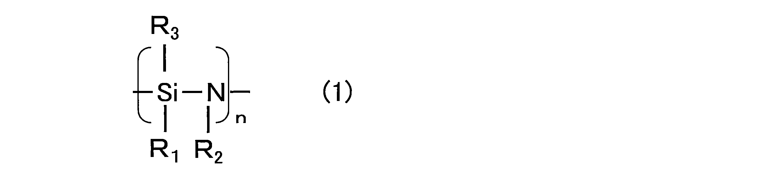
本発明において無機層[A]のケイ素化合物層[B]側の界面領域[I]におけるX線光電子分光法で得られるZnLMMスペクトル(例を、図4太線に示す)が、無機層[A]の中央部における同スペクトル(例を、図4細線に示す)に対し、相対的にブロードであることが好ましい。ここで、ZnLMMスペクトルが相対的にブロードであるとは、ピークトップの強度を1に規格化したときの強度0.4におけるスペクトルの幅の比較に基づくものとする。さらに、スペクトルがブロードとなる場合に、スペクトルの低結合エネルギー側(図4における横軸の右側方向が低結合エネルギー側方向に相当)がブロードになっていることがより好ましい。
本発明のガスバリア性フィルムには、ガスバリア性向上、耐屈曲性向上のため、前記高分子基材と前記無機層[A]との間に芳香族環構造を有するポリウレタン化合物[C1]を架橋して得られる構造を含むアンダーコート層[C]を設けることが好ましい。高分子基材上に突起や小擦り傷などの欠点が存在する場合、前記欠点を起点に高分子基材上に積層する無機層[A]にもピンホールやクラックが発生してガスバリア性や耐屈曲性が損なわれる場合があるため、本発明のアンダーコート層[C]を設けるのが好ましい。また、高分子基材と無機層[A]との熱寸法安定性差が大きい場合もガスバリア性や耐屈曲性が低下する場合があるため、本発明のアンダーコート層[C]を設けるのが好ましい。また、本発明に用いられるアンダーコート層[C]は、熱寸法安定性、耐屈曲性の観点から芳香族環構造を有するポリウレタン化合物[C1]を含有することが好ましく、さらに、エチレン性不飽和化合物[C2]、光重合開始剤[C3]、有機ケイ素化合物[C4]および/または無機ケイ素化合物[C5]を含有することがより好ましい。
本発明に用いられる芳香族環構造を有するポリウレタン化合物[C1]は、主鎖あるいは側鎖に芳香族環およびウレタン結合を有するものであり、例えば、分子内に水酸基と芳香族環とを有するエポキシ(メタ)アクリレート(c1)、ジオール化合物(c2)、ジイソシアネート化合物(c3)とを重合させて得ることができる。
エチレン性不飽和化合物[C2]としては、例えば、1,4-ブタンジオールジ(メタ)アクリレート、1,6-ヘキサンジオールジ(メタ)アクリレート等のジ(メタ)アクリレート、ペンタエリスリトールトリ(メタ)アクリレート、ペンタエリスリトールテトラ(メタ)アクリレート、ジペンタエリスリトールテトラ(メタ)アクリレート、ジペンタエリスリトールペンタ(メタ)アクリレート、ジペンタエリスリトールヘキサ(メタ)アクリレート等の多官能(メタ)アクリレート、ビスフェノールA型エポキシジ(メタ)アクリレート、ビスフェノールF型エポキシジ(メタ)アクリレート、ビスフェノールS型エポキシジ(メタ)アクリレート等のエポキシアクリレート等を挙げられる。これらの中でも、熱寸法安定性、表面保護性能に優れた多官能(メタ)アクリレートが好ましい。また、これらは単一の組成で用いてもよいし、二成分以上を混合して使用してもよい。
光重合開始剤[C3]としては、本発明のガスバリア性フィルムのガスバリア性および耐屈曲性を保持することができれば素材は特に限定されない。本発明に好適に用いることができる光重合開始剤としては、例えば、2,2-ジメトキシ-1,2-ジフェニルエタン-1-オン、1-ヒドロキシ-シクロヘキシルフェニルーケトン、2-ヒドロキシ-2-メチル-1-フェニル-プロパン-1-オン、1-[4-(2-ヒドロキシエトキシ)-フェニル]-2-ヒドロキシ-2-メチル-1-プロパン-1-オン、2-ヒロドキシ-1-{4-[4-(2-ヒドロキシ-2-メチル-プロピオニル)-ベンジル]フェニル}-2-メチル-プロパン-1-オン、フェニルグリオキシリックアシッドメチルエステル、2-メチル-1-(4-メチルチオフェニル)-2-モルホリノプロパン-1-オン、2-ベンジル-2-ジメチルアミノ-1-(4-モルホリノフェニル)-ブタノン-1、2-(ジメチルアミノ)-2-[(4-メチルフェニル)メチル]-1-[4-(4-モルホリニル)フェニル]-1-ブタノン等のアルキルフェノン系光重合開始剤、2,4,6-トリメチルベンゾイル-ジフェニル-ホスフィンオキシド、ビス(2,4,6-トリメチルベンゾイル)-フェニルホスフィンオキシド等のアシルホスフィンオキシド系光重合開始剤、ビス(η5-2,4-シクロペンタジエン-1-イル)-ビス(2,6-ジフルオロ-3-(1H-ピロール-1-イル)-フェニル)チタニウム等のチタノセン系光重合開始剤、1,2-オクタンジオン,1-[4-(フェニルチオ)-,2-(0-ベンゾイルオキシム)]等オキシムエステル構造を持つ光重合開始剤等が挙げられる。
有機ケイ素化合物[C4]としては、例えば、ビニルトリメトキシシラン、ビニルトリエトキシシラン、2-(3,4-エポキシシクロヘキシル)エチルトリメトキシシラン、3-グリシドキシプロピルメチルジメトキシシラン、3-グリシドキシプロピルトリメトキシシラン、3-グリシドキシプロピルメチルジエトキシシラン、3-グリシドキシプロピルトリエトキシシラン、3-メタクリロキシプロピルメチルジメトキシシラン、3-メタクリロキシプロピルトリメトキシシラン、3-メタクリロキシプロピルメチルジエトキシシラン、3-メタクリロキシプロピルトリエトキシシラン、3-アクリロキシプロピルトリメトキシシラン、N-2-(アミノエチル)-3-アミノプロピルメチルジメトキシシラン、N-2-(アミノエチル)-3-アミノプロピルトリメトキシシラン、3-アミノプロピルトリメトキシシラン、3-アミノプロピルトリエトキシシラン、3-イソシアネートプロピルトリエトキシシラン等が挙げられる。
無機ケイ素化合物[C5]としては、表面保護性能、透明性の観点からシリカ粒子が好ましく、さらにシリカ粒子の一次粒子径が1~300nmの範囲であることが好ましく、5~80nmの範囲であることがより好ましい。なお、ここでいう一次粒子径とは、ガス吸着法により求めた比表面積sを下記の式(1)に適用することで求められる粒子直径dを指す。
アンダーコート層[C]の厚みは、200nm以上、4,000nm以下が好ましい。アンダーコート層[C]の厚みが200nmより薄くなると、高分子基材上に存在する突起や小擦り傷などの欠点の悪影響を抑制できない場合がある。アンダーコート層[C]の厚みが4,000nmより厚くなると、アンダーコート層[C]の平滑性が低下して前記アンダーコート層[C]上に積層する無機層[A]表面の凹凸形状も大きくなり、積層されるスパッタ粒子間に隙間ができるため、膜質が緻密になりにくく、ガスバリア性の向上効果が得られにくくなる場合がある。従って、アンダーコート層[C]の厚みは200nm以上、4,000nm以下が好ましい。ケイ素化合物層[B]の厚みは、透過型電子顕微鏡(TEM)による断面観察画像から測定することが可能である。
本発明のガスバリア性フィルムの最表面の上には、ガスバリア性が低下しない範囲で耐擦傷性の向上を目的としたハードコート層を形成してもよいし、有機高分子化合物からなるフィルムをラミネートした積層構成としてもよい。なお、ここでいう最表面とは、高分子基材上に無機層[A]およびケイ素化合物層[B]が接するようにこの順に積層された後の、無機層[A]と接していない側のケイ素化合物層[B]の表面をいう。
本発明のガスバリア性フィルムの製造方法について以下に詳細を説明する。
工程aでは、簡便かつ緻密に無機層を形成可能であるため、図2に示す構造の巻き取り式のスパッタリング装置を使用することが好ましい。無機層[A]の組成は、層の形成時に使用した混合焼結材料と同様の組成で形成されるため、目的とする層の組成に合わせた組成の混合焼結材料を使用することで組成を調整することが可能である。
工程bでは、まず無機層[A]上にポリシラザン骨格を持つケイ素化合物を含む塗料を乾燥後の厚みが所望の厚みになるよう固形分濃度を調整しリバースコート法、グラビアコート法、ロッドコート法、バーコート法、ダイコート法、スプレーコート法、スピンコート法などにより塗布することが好ましい。ここでポリシラザン骨格を持つケイ素化合物としては、パーヒドロポリシラザン、オルガノポリシラザン、およびこれらの誘導体より選択される一種または二種以上を組み合わせて用いることができる。
本発明においては、必要に応じて工程cによりアンダーコート層[C]を設けることができる。工程cでは、まず高分子基材上に芳香族環構造を有するポリウレタン化合物[C1]を含む塗料を乾燥後の厚みが所望の厚みになるよう固形分濃度を調整し、例えばリバースコート法、グラビアコート法、ロッドコート法、バーコート法、ダイコート法、スプレーコート法、スピンコート法などにより塗布することが好ましい。また、本発明においては、塗工適性の観点から有機溶剤を用いて芳香族環構造を有するポリウレタン化合物[C1]を含む塗料を希釈することが好ましい。具体的には、キシレン、トルエン、メチルシクロヘキサン、ペンタン、ヘキサンなどの炭化水素系溶剤、ジブチルエーテル、エチルブチルエーテル、テトラヒドロフランなどのエーテル系溶剤などを用いて、固形分濃度が10質量%以内に希釈して使用することが好ましい。これらの溶剤は、単独あるいは2種以上を混合して用いてもよい。また、アンダーコート層[C]を形成する塗料には、各種の添加剤を必要に応じて配合することができる。例えば、触媒、酸化防止剤、光安定剤、紫外線吸収剤などの安定剤、界面活性剤、レベリング剤、帯電防止剤などを用いることができる。
本発明の電子デバイスは、本発明のガスバリア性フィルムを有するため、本発明の電子デバイスは優れたガスバリア性を有し、水蒸気等によるデバイスの性能低下を抑制することができる。
まず、各実施例および比較例における評価方法を説明する。特に記載のない限り評価n数は水準当たり5検体とし、得られた5検体の測定値の平均値を測定結果とした。
断面観察用サンプルをマイクロサンプリングシステム((株)日立製作所製 FB-2000A)を使用してFIB法により(具体的には「高分子表面加工学」(岩森暁著)p.118~119に記載の方法に基づいて)作製した。透過型電子顕微鏡((株)日立製作所製 H-9000UHRII)により、加速電圧300kVとして、観察用サンプルの断面を観察し、無機層[A]、ケイ素化合物層[B]、アンダーコート層[C]の厚みを測定した。
三次元表面粗さ測定機(小坂研究所社製)を用いて、以下の条件で各層表面について測定した。
システム:三次元表面粗さ解析システム「i-Face model TDA31」
X軸測定長さ/ピッチ:500μm/1.0μm
Y軸測定長さ/ピッチ:400μm/5.0μm
測定速度:0.1mm/s
測定環境:温度23℃、相対湿度65%RH、大気中。
特許第4407466号に記載のカルシウム腐食法により、温度40℃、相対湿度90%RHの雰囲気下での水蒸気透過度を測定した。水蒸気透過度サンプル数は水準当たり2検体とし、測定回数は各検体について5回とし、得られた10点の平均値を水蒸気透過度(g/(m2・d))とした。
[A1]の組成分析はICP発光分光分析(エスアイアイ・ナノテクノロジー社製、SPS4000)により行った。高分子基材に無機層[A1]を形成した段階(ケイ素化合物層[B]を積層する前)でサンプリングした試料を硝酸および硫酸で加熱分解し、希硝酸で加温溶解してろ別した。不溶解分は加熱灰化したのち、炭酸ナトリウムで融解し、希硝酸で溶解して、先のろ液とあわせて定容とした。この溶液について、亜鉛原子、ケイ素原子、アルミニウム原子の含有量を測定し、原子数比に換算した。なお、酸素原子は亜鉛原子、ケイ素原子、アルミニウム原子が、それぞれ酸化亜鉛(ZnO)、二酸化ケイ素(SiO2)、酸化アルミニウム(Al2O3)として存在すると仮定して求めた計算値とした。
無機層[A2]の組成分析はICP発光分光分析(エスアイアイ・ナノテクノロジー社製、SPS4000)により行った。高分子基材に無機層[A2]を形成した段階(ケイ素化合物層[B]を積層する前)でサンプリングした試料を、硝酸および硫酸で加熱分解し、希硝酸で加温溶解してろ別した。不溶解分は加熱灰化したのち、炭酸ナトリウムで融解し、希硝酸で溶解して、先のろ液とあわせて定容とした。この溶液について、亜鉛原子、ケイ素原子の含有量を測定した。次に、この値をもとにさらにラザフォード後方散乱法(日新ハイボルテージ(株)製 AN-2500)を使用して、亜鉛原子、ケイ素原子、硫黄原子、酸素原子を定量分析し、硫化亜鉛と二酸化ケイ素の組成比を求めた。
X線光電子分光法(XPS法)を用いて、炭素、窒素、酸素、アルミニウム、ケイ素、亜鉛について深さ方向に組成分析を行い、図3に例を示したような元素分布を求めた。各深さにおけるケイ素原子に対する酸素原子の原子組成比およびケイ素原子に対する窒素原子の原子組成比を算出し、その最大値と最小値とを得た。また、界面領域[I]有無についても前記組成比算出時に確認した。測定条件は下記の通りとした。
装置:Quantera SXM (PHI社製)
励起X線:monochromatic Al Kα1,2線(1486.6eV)
X線径:100μm
光電子脱出角度(試料表面に対する検出器の傾き):45°
イオンエッチング:Ar+ ion 2kV
raster サイズ : 2×2mm。
図5に示すとおり、ガスバリア性フィルムを100mm×140mmに水準当たり2検体サンプリングし、このサンプルにおいて、無機層[A]およびケイ素化合物層[B]が形成された面と反対面側の中央部に直径5mmの金属円柱を固定し、この円柱に沿って、円柱の抱き角0°(サンプルが平面の状態)から、円柱への抱き角が180°(円柱で折り返した状態)となる範囲で、100回折り曲げ動作を行った後、(3)に示す方法で水蒸気透過度評価を行った。測定回数は各検体について5回とし、得られた10点の平均値を耐屈曲性試験後の水蒸気透過度とした。
(無機層[A1]の形成)
図2に示す構造の巻き取り式のスパッタリング装置を使用し、高分子基材の片面に酸化亜鉛と二酸化ケイ素と酸化アルミニウムで形成された混合焼結材であるスパッタターゲットを用いてスパッタリングを実施し無機層[A1]を設けた。
図2に示す構造の巻き取り式のスパッタリング装置を使用し、高分子基材の片面に、硫化亜鉛および二酸化ケイ素で形成された混合焼結材であるスパッタターゲットを用いてスパッタリングを実施し無機層[A2]を設けた。
5リットルの4つ口フラスコに、ビスフェノールAジグリシジルエーテルアクリル酸付加物(共栄社化学社製、商品名:エポキシエステル3000A)300質量部と、酢酸エチル710質量部とを入れ、内温60℃になるよう加温した。合成触媒としてジラウリン酸ジ-n-ブチル錫0.2質量部を添加し、攪拌しながらジシクロヘキシルメタン4,4’-ジイソシアネート(東京化成工業社製)200質量部を1時間かけて滴下した。滴下終了後2時間反応を続行し、続いてジエチレングリコール(和光純薬工業社製)25質量部を1時間かけて滴下した。滴下後5時間反応を続行し、重量平均分子量20,000の芳香族環構造を有するポリウレタン化合物を得た。
高分子基材として厚み50μmのポリエチレンテレフタレートフィルム(東レ株式会社製 “ルミラー”(登録商標)U48)を使用し、この高分子基材の片面に無機層[A1]を厚み180nmとなるよう設けた。無機層[A1]の組成は、Zn原子濃度が27.5atom%、Si原子濃度が13.1atom%、Al原子濃度が2.3atom%、O原子濃度が57.1atom%であった。無機層[A1]を形成したフィルムから縦100mm、横100mmの試験片を切り出し、無機層[A1]の中心面平均粗さSRaの評価を実施した。結果を表1に示す。
導入ガス:N2
積算光量:3,000mJ/cm2
試料温調:100℃
得られたガスバリア性フィルムにX線光電子分光法(XPS法)を用いて、組成分析を行い、深さ方向の元素分布を求めた。各深さにおけるケイ素原子に対する酸素原子の原子組成比およびケイ素原子に対する窒素原子の原子組成比を算出し、その最大値(max)と最小値(min)とを表1に示す。
高分子基材として厚み50μmのポリエチレンテレフタレートフィルム(東レ株式会社製 “ルミラー”(登録商標)U48)を使用した。
アンダーコート層[C]形成用の塗液として、前記ポリウレタン化合物150質量部と、ジペンタエリスリトールヘキサアクリレート(共栄社化学社製、商品名:ライトアクリレートDPE-6A)20質量部と、1-ヒドロキシ-シクロヘキシルフェニルーケトン(BASFジャパン社製、商品名:IRGACURE 184)5質量部と、3-メタクリロキシプロピルメチルジエトキシシラン(信越シリコーン社製、商品名:KBM-503)3質量部と、酢酸エチル170質量部と、トルエン350質量部と、シクロヘキサノン170質量部とを配合して塗液2を調整した。次いで、塗液2を高分子基材上にマイクログラビアコーター(グラビア線番150UR、グラビア回転比100%)で塗布、100℃で1分間乾燥し、乾燥後、下記条件にて紫外線処理を施して厚み1,000nmのアンダーコート層[C]を設けた。
導入ガス:N2(窒素イナートBOX)
紫外線発生源:マイクロ波方式無電極ランプ
積算光量:400mJ/cm2
試料温調:室温。
導入ガス:N2
紫外線発生源:エキシマランプ(172nm)
積算光量:3,000mJ/cm2
試料温調:100℃
得られたガスバリア性フィルムから縦100mm、横140mmの試験片を切り出し、水蒸気透過度の評価を実施した。結果を表1に示す。
高分子基材として厚み100μmの非晶性環状ポリオレフィンフィルム(日本ゼオン社製 “ゼオノアフィルム”ZF14)を使用した以外は、実施例1と同様にしてガスバリア性フィルムを得た。
高分子基材として厚み100μmの非晶性環状ポリオレフィンフィルム(日本ゼオン社製 “ゼオノアフィルム”ZF14)を使用した以外は、実施例2と同様にしてガスバリア性フィルムを得た。
無機層[A1]を厚み950nmとなるよう設けた以外は、実施例2と同様にしてガスバリア性フィルムを得た。
無機層[A1]に代えて無機層[A2]を厚み150nmとなるよう設けた以外は、実施例2と同様にしてガスバリア性フィルムを得た。
ケイ素化合物層[B]を厚み50nmとなるよう設けた以外は、実施例2と同様にしてガスバリア性フィルムを得た。
ケイ素化合物層[B]を厚み1,000nmとなるよう設けた以外は、実施例2と同様にしてガスバリア性フィルムを得た。
ケイ素化合物層[B]用塗料を塗布し乾燥後、紫外線処理の代わりに窒素雰囲気下で80℃、3日間処理してケイ素化合物層[B]を設ける以外は、実施例2と同様にしてガスバリア性フィルムを得た。
ケイ素化合物層[B]用塗料として、パーヒドロポリシラザンを主成分とし、アミン系触媒を含むコート剤(AZエレクトロニックマテリアルズ社製「NAX120-20」、固形分濃度20質量部)100質量部をジブチルエーテル300質量部で希釈した塗液を用いる以外は、実施例2と同様にしてガスバリア性フィルムを得た。
ケイ素化合物層[B]用塗料として、パーヒドロポリシラザンを主成分とし、触媒を含まないコート剤(AZエレクトロニックマテリアルズ社製「NN120-20」、固形分濃度20質量部)100質量部をジブチルエーテル300質量部で希釈した塗液を用いる以外は、実施例2と同様にしてガスバリア性フィルムを得た。
高分子基材上に無機層[A]を形成しないで、高分子基材の表面に直接、ケイ素化合物層[B]を厚み120nmとなるように設けた以外は、実施例1と同様にしてガスバリア性フィルムを得た。
無機層[A]上にケイ素化合物層[B]設けない以外は、実施例1と同様にしてガスバリア性フィルムを得た。
実施例1において、無機層[A]とケイ素化合物層[B]とを形成する順序を入れ替え、実施例1と層構成が異なるガスバリアフィルムを得た。

2 無機層[A]
3 ケイ素化合物層[B]
4 アンダーコート層[C]
5 高分子基材
6 巻き取り式スパッタリング装置
7 巻き取り室
8 巻き出しロール
9、10、11 巻き出し側ガイドロール
12 クーリングドラム
13 スパッタ電極
14、15、16 巻き取り側ガイドロール
17 巻き取りロール
18 ガスバリア性フィルム
19 金属円柱
20 無機層[A]およびケイ素化合物層[B]が形成された面と反対面
Claims (10)
- 高分子基材の少なくとも片側に、無機層[A]と、ケイ素化合物層[B]とを前記高分子基材側からこの順に有するガスバリア性フィルムであって、無機層[A]が、亜鉛化合物とケイ素酸化物とを含み、ケイ素化合物層[B]が、ケイ素酸窒化物を含み、かつ無機層[A]とケイ素化合物層[B]が接しているガスバリア性フィルム。
- 前記高分子基材と前記無機層[A]との間に、芳香族環構造を有するポリウレタン化合物[C1]を架橋して得られる構造を含むアンダーコート層[C]を有する請求項1に記載のガスバリア性フィルム。
- 前記無機層[A]が、酸化亜鉛と二酸化ケイ素と酸化アルミニウムの共存相からなる無機層[A1]または硫化亜鉛と二酸化ケイ素の共存相からなる無機層[A2]のいずれかである請求項1または2に記載のガスバリア性フィルム。
- 前記無機層[A]が前記無機層[A1]であり、該無機層[A1]が、ICP発光分光分析法により測定される亜鉛原子濃度が20~40atom%、ケイ素原子濃度が5~20atom%、アルミニウム原子濃度が0.5~5atom%、酸素原子濃度が35~70atom%である組成により構成されたものである請求項3に記載のガスバリア性フィルム。
- 前記無機層[A]が前記無機層[A2]であり、該無機層[A2]は、硫化亜鉛と二酸化ケイ素の合計に対する硫化亜鉛のモル分率が0.7~0.9である組成により構成されたものである請求項3に記載のガスバリア性フィルム。
- 前記ケイ素化合物層[B]が、X線光電子分光法で元素分布を測定した際に、ケイ素原子に対する酸素原子の原子組成比が0.1以上、2.0未満、かつケイ素原子に対する窒素原子の原子組成比が0.1以上、1.0未満である請求項1~5のいずれかに記載のガスバリア性フィルム。
- 前記アンダーコート層[C]が有機ケイ素化合物および/または無機ケイ素化合物を含む請求項2~6のいずれかに記載のガスバリア性フィルム。
- 請求項1~7のいずれかに記載のガスバリア性フィルムを有する電子デバイス。
- 高分子基材上に、スパッタリング法により亜鉛化合物とケイ素酸化物とを含む無機層[A]を設ける工程aと、該無機層[A]上に、ポリシラザン骨格を持つケイ素化合物を含む塗液を塗布後乾燥させて塗膜を形成し、次いで該塗膜に窒素雰囲気下で活性エネルギー線照射処理をしてケイ素酸窒化物を含むケイ素化合物層[B]を設ける工程bとを含むガスバリア性フィルムの製造方法。
- 高分子基材上に、芳香族環構造を有するポリウレタン化合物[C1]を含む塗液を塗布後乾燥させて塗膜を形成し、次いで該塗膜に窒素雰囲気下で活性エネルギー線照射処理をしてアンダーコート層[C]を設ける工程cと、該アンダーコート層[C]上に、スパッタリング法により亜鉛化合物とケイ素酸化物とを含む無機層[A]を設ける工程aと、該無機層[A]上に、ポリシラザン骨格を持つケイ素化合物を含む塗液を塗布後乾燥させて塗膜を形成し、次いで該塗膜に窒素雰囲気下で活性エネルギー線照射処理をしてケイ素酸化物とケイ素酸窒化物とを含むケイ素化合物層[B]を設ける工程bとを含むガスバリア性フィルムの製造方法。
Priority Applications (5)
| Application Number | Priority Date | Filing Date | Title |
|---|---|---|---|
| US14/759,829 US10829643B2 (en) | 2013-01-11 | 2013-12-25 | Gas barrier film |
| CN201380069794.0A CN104903089A (zh) | 2013-01-11 | 2013-12-25 | 阻气性膜 |
| JP2014502934A JP6269476B2 (ja) | 2013-01-11 | 2013-12-25 | ガスバリア性フィルム |
| EP13870926.6A EP2944460B1 (en) | 2013-01-11 | 2013-12-25 | Gas barrier film |
| KR1020157020327A KR102196648B1 (ko) | 2013-01-11 | 2013-12-25 | 가스 배리어성 필름 |
Applications Claiming Priority (4)
| Application Number | Priority Date | Filing Date | Title |
|---|---|---|---|
| JP2013-003089 | 2013-01-11 | ||
| JP2013003089 | 2013-01-11 | ||
| JP2013-236569 | 2013-11-15 | ||
| JP2013236569 | 2013-11-15 |
Publications (1)
| Publication Number | Publication Date |
|---|---|
| WO2014109231A1 true WO2014109231A1 (ja) | 2014-07-17 |
Family
ID=51166888
Family Applications (1)
| Application Number | Title | Priority Date | Filing Date |
|---|---|---|---|
| PCT/JP2013/084626 WO2014109231A1 (ja) | 2013-01-11 | 2013-12-25 | ガスバリア性フィルム |
Country Status (7)
| Country | Link |
|---|---|
| US (1) | US10829643B2 (ja) |
| EP (1) | EP2944460B1 (ja) |
| JP (1) | JP6269476B2 (ja) |
| KR (1) | KR102196648B1 (ja) |
| CN (2) | CN104903089A (ja) |
| TW (1) | TWI608934B (ja) |
| WO (1) | WO2014109231A1 (ja) |
Cited By (11)
| Publication number | Priority date | Publication date | Assignee | Title |
|---|---|---|---|---|
| KR20160020834A (ko) * | 2014-08-14 | 2016-02-24 | 엘에스엠트론 주식회사 | 배리어 필름 구조체 및 이를 구비하는 유기전자소자 |
| WO2016052123A1 (ja) * | 2014-09-30 | 2016-04-07 | 東レ株式会社 | ガスバリア性フィルム、それを用いた電子デバイス、およびガスバリア性フィルムの製造方法 |
| JP2016064650A (ja) * | 2014-09-16 | 2016-04-28 | 東レ株式会社 | ガスバリア性フィルム |
| JP2016124123A (ja) * | 2014-12-26 | 2016-07-11 | 東レ株式会社 | 積層体 |
| JP2016172399A (ja) * | 2015-03-17 | 2016-09-29 | コニカミノルタ株式会社 | ガスバリア性フィルムの製造方法 |
| JP2017065054A (ja) * | 2015-09-30 | 2017-04-06 | 東レ株式会社 | ガスバリア性フィルムおよび電子デバイス |
| JP2018001521A (ja) * | 2016-06-30 | 2018-01-11 | 東レ株式会社 | ガスバリア性フィルム |
| JPWO2016171184A1 (ja) * | 2015-04-22 | 2018-02-15 | リンテック株式会社 | ガスバリアフィルム、電子デバイス用部材、および電子デバイス |
| WO2018043127A1 (ja) * | 2016-08-29 | 2018-03-08 | 東レ株式会社 | 積層体 |
| JP2018052068A (ja) * | 2016-09-30 | 2018-04-05 | 三菱ケミカル株式会社 | 積層フィルム及びその製造方法 |
| WO2018207508A1 (ja) * | 2017-05-12 | 2018-11-15 | 富士フイルム株式会社 | ガスバリアフィルムおよびガスバリアフィルムの製造方法 |
Families Citing this family (6)
| Publication number | Priority date | Publication date | Assignee | Title |
|---|---|---|---|---|
| CN104716270A (zh) * | 2015-03-16 | 2015-06-17 | 上海和辉光电有限公司 | 一种薄膜封装结构和具有该结构的有机发光装置 |
| WO2017159787A1 (ja) * | 2016-03-18 | 2017-09-21 | リンテック株式会社 | プライマー層形成用硬化性組成物、ガスバリア性積層フィルムおよびガスバリア性積層体 |
| JP2018154012A (ja) * | 2017-03-17 | 2018-10-04 | コニカミノルタ株式会社 | 機能性フィルム、及び、電子デバイスの製造方法 |
| JP6935219B2 (ja) * | 2017-03-31 | 2021-09-15 | 三井化学東セロ株式会社 | バリア性積層フィルム |
| CN110172674A (zh) * | 2019-05-29 | 2019-08-27 | 汕头万顺新材集团股份有限公司 | 一种高透明性阻隔膜及其制备方法 |
| CN112760036A (zh) * | 2019-11-05 | 2021-05-07 | 中国科学院化学研究所 | 一种具有紫外光屏蔽、可见光增透性能的耐原子氧涂层及其制备方法 |
Citations (10)
| Publication number | Priority date | Publication date | Assignee | Title |
|---|---|---|---|---|
| JPH08142252A (ja) | 1994-11-22 | 1996-06-04 | Dainippon Printing Co Ltd | バリアー性フィルムおよびその製造方法 |
| JP2002113826A (ja) | 2000-10-06 | 2002-04-16 | Toppan Printing Co Ltd | プラスチック基材及びそれを用いたガスバリアフィルム |
| WO2008035557A1 (fr) * | 2006-09-22 | 2008-03-27 | Toray Industries, Inc. | Film barrière aux gaz |
| JP4407466B2 (ja) | 2004-10-25 | 2010-02-03 | 住友ベークライト株式会社 | カルシウム腐食法による水蒸気透過度測定方法 |
| WO2011004698A1 (ja) | 2009-07-10 | 2011-01-13 | コニカミノルタホールディングス株式会社 | ガスバリアフィルムとその製造方法、これを用いた光電変換素子 |
| WO2011007543A1 (ja) | 2009-07-17 | 2011-01-20 | 三井化学株式会社 | 積層体およびその製造方法 |
| JP2011201302A (ja) * | 2010-03-02 | 2011-10-13 | Toray Ind Inc | ガスバリア性フィルム |
| WO2012137662A1 (ja) | 2011-04-05 | 2012-10-11 | 東レ株式会社 | ガスバリア性フィルム |
| JP2012206507A (ja) * | 2011-03-11 | 2012-10-25 | Toray Ind Inc | ガスバリア性フィルム |
| WO2013061726A1 (ja) | 2011-10-28 | 2013-05-02 | 東レ株式会社 | ガスバリア性フィルム |
Family Cites Families (14)
| Publication number | Priority date | Publication date | Assignee | Title |
|---|---|---|---|---|
| JP4524463B2 (ja) * | 1999-07-27 | 2010-08-18 | 三井化学株式会社 | ガスバリア性ポリウレタン樹脂及びこれを含むガスバリア性フィルム |
| US20050037240A1 (en) * | 2003-03-31 | 2005-02-17 | Daisaku Haoto | Protective coat and method for manufacturing thereof |
| JP3951055B2 (ja) * | 2004-02-18 | 2007-08-01 | セイコーエプソン株式会社 | 有機エレクトロルミネッセンス装置及び電子機器 |
| EP1760126A4 (en) * | 2004-06-11 | 2010-02-24 | Toray Industries | SILOXANE COATING MATERIAL, OPTICAL ARTICLES AND PROCESSES FOR THE PRODUCTION OF SILOXANE COATING MATERIALS |
| US20060023735A1 (en) * | 2004-07-28 | 2006-02-02 | Nir Sasson | Versatile low power driver for gigabit ethernet systems |
| JP4630032B2 (ja) * | 2004-10-04 | 2011-02-09 | 東レ・ダウコーニング株式会社 | ポリオルガノシロキサン及びそれを含む硬化性シリコーン組成物並びにその用途 |
| CN100595317C (zh) * | 2004-10-19 | 2010-03-24 | 东丽株式会社 | 薄膜的制造方法和薄膜 |
| US7790634B2 (en) | 2006-05-30 | 2010-09-07 | Applied Materials, Inc | Method for depositing and curing low-k films for gapfill and conformal film applications |
| WO2009134211A1 (en) * | 2008-04-29 | 2009-11-05 | Agency For Science, Technology And Research | Inorganic graded barrier film and methods for their manufacture |
| US20100132762A1 (en) * | 2008-12-02 | 2010-06-03 | Georgia Tech Research Corporation | Environmental barrier coating for organic semiconductor devices and methods thereof |
| CN102712828A (zh) * | 2010-01-07 | 2012-10-03 | 道康宁东丽株式会社 | 具有阻气性的固化的有机聚硅氧烷树脂膜和生产该树脂膜的方法 |
| KR20140004143A (ko) * | 2011-02-25 | 2014-01-10 | 미쓰비시 마테리알 가부시키가이샤 | 투명 산화물막 및 그 제조 방법 |
| JP5760857B2 (ja) | 2011-08-29 | 2015-08-12 | 三菱マテリアル株式会社 | スパッタリングターゲット及びその製造方法並びに該ターゲットを用いた薄膜、該薄膜を備える薄膜シート、積層シート |
| KR102051328B1 (ko) | 2011-09-07 | 2019-12-03 | 도레이 카부시키가이샤 | 가스 배리어성 필름 |
-
2013
- 2013-12-25 EP EP13870926.6A patent/EP2944460B1/en active Active
- 2013-12-25 US US14/759,829 patent/US10829643B2/en active Active
- 2013-12-25 CN CN201380069794.0A patent/CN104903089A/zh active Pending
- 2013-12-25 CN CN201810245065.0A patent/CN108503870B/zh active Active
- 2013-12-25 JP JP2014502934A patent/JP6269476B2/ja active Active
- 2013-12-25 KR KR1020157020327A patent/KR102196648B1/ko active IP Right Grant
- 2013-12-25 WO PCT/JP2013/084626 patent/WO2014109231A1/ja active Application Filing
- 2013-12-27 TW TW102148590A patent/TWI608934B/zh active
Patent Citations (10)
| Publication number | Priority date | Publication date | Assignee | Title |
|---|---|---|---|---|
| JPH08142252A (ja) | 1994-11-22 | 1996-06-04 | Dainippon Printing Co Ltd | バリアー性フィルムおよびその製造方法 |
| JP2002113826A (ja) | 2000-10-06 | 2002-04-16 | Toppan Printing Co Ltd | プラスチック基材及びそれを用いたガスバリアフィルム |
| JP4407466B2 (ja) | 2004-10-25 | 2010-02-03 | 住友ベークライト株式会社 | カルシウム腐食法による水蒸気透過度測定方法 |
| WO2008035557A1 (fr) * | 2006-09-22 | 2008-03-27 | Toray Industries, Inc. | Film barrière aux gaz |
| WO2011004698A1 (ja) | 2009-07-10 | 2011-01-13 | コニカミノルタホールディングス株式会社 | ガスバリアフィルムとその製造方法、これを用いた光電変換素子 |
| WO2011007543A1 (ja) | 2009-07-17 | 2011-01-20 | 三井化学株式会社 | 積層体およびその製造方法 |
| JP2011201302A (ja) * | 2010-03-02 | 2011-10-13 | Toray Ind Inc | ガスバリア性フィルム |
| JP2012206507A (ja) * | 2011-03-11 | 2012-10-25 | Toray Ind Inc | ガスバリア性フィルム |
| WO2012137662A1 (ja) | 2011-04-05 | 2012-10-11 | 東レ株式会社 | ガスバリア性フィルム |
| WO2013061726A1 (ja) | 2011-10-28 | 2013-05-02 | 東レ株式会社 | ガスバリア性フィルム |
Non-Patent Citations (2)
| Title |
|---|
| "Kobunshi Hyomen Kako (Polymer Surface Processing)", SATORU IWAMORI, pages: 118 - 119 |
| See also references of EP2944460A4 |
Cited By (16)
| Publication number | Priority date | Publication date | Assignee | Title |
|---|---|---|---|---|
| KR20160020834A (ko) * | 2014-08-14 | 2016-02-24 | 엘에스엠트론 주식회사 | 배리어 필름 구조체 및 이를 구비하는 유기전자소자 |
| KR102343768B1 (ko) * | 2014-08-14 | 2021-12-24 | 에스케이넥실리스 주식회사 | 배리어 필름 구조체 및 이를 구비하는 유기전자소자 |
| JP2016064650A (ja) * | 2014-09-16 | 2016-04-28 | 東レ株式会社 | ガスバリア性フィルム |
| WO2016052123A1 (ja) * | 2014-09-30 | 2016-04-07 | 東レ株式会社 | ガスバリア性フィルム、それを用いた電子デバイス、およびガスバリア性フィルムの製造方法 |
| JPWO2016052123A1 (ja) * | 2014-09-30 | 2017-07-13 | 東レ株式会社 | ガスバリア性フィルム、それを用いた電子デバイス、およびガスバリア性フィルムの製造方法 |
| JP2016124123A (ja) * | 2014-12-26 | 2016-07-11 | 東レ株式会社 | 積層体 |
| JP2016172399A (ja) * | 2015-03-17 | 2016-09-29 | コニカミノルタ株式会社 | ガスバリア性フィルムの製造方法 |
| JPWO2016171184A1 (ja) * | 2015-04-22 | 2018-02-15 | リンテック株式会社 | ガスバリアフィルム、電子デバイス用部材、および電子デバイス |
| JP2017065054A (ja) * | 2015-09-30 | 2017-04-06 | 東レ株式会社 | ガスバリア性フィルムおよび電子デバイス |
| JP2018001521A (ja) * | 2016-06-30 | 2018-01-11 | 東レ株式会社 | ガスバリア性フィルム |
| WO2018043127A1 (ja) * | 2016-08-29 | 2018-03-08 | 東レ株式会社 | 積層体 |
| KR20190045218A (ko) * | 2016-08-29 | 2019-05-02 | 도레이 카부시키가이샤 | 적층체 |
| JPWO2018043127A1 (ja) * | 2016-08-29 | 2019-06-24 | 東レ株式会社 | 積層体 |
| KR102374301B1 (ko) * | 2016-08-29 | 2022-03-15 | 도레이 카부시키가이샤 | 적층체 |
| JP2018052068A (ja) * | 2016-09-30 | 2018-04-05 | 三菱ケミカル株式会社 | 積層フィルム及びその製造方法 |
| WO2018207508A1 (ja) * | 2017-05-12 | 2018-11-15 | 富士フイルム株式会社 | ガスバリアフィルムおよびガスバリアフィルムの製造方法 |
Also Published As
| Publication number | Publication date |
|---|---|
| JPWO2014109231A1 (ja) | 2017-01-19 |
| KR102196648B1 (ko) | 2020-12-30 |
| US10829643B2 (en) | 2020-11-10 |
| KR20150104582A (ko) | 2015-09-15 |
| EP2944460A1 (en) | 2015-11-18 |
| JP6269476B2 (ja) | 2018-01-31 |
| TWI608934B (zh) | 2017-12-21 |
| EP2944460A4 (en) | 2016-09-07 |
| CN108503870A (zh) | 2018-09-07 |
| EP2944460B1 (en) | 2019-08-28 |
| TW201431686A (zh) | 2014-08-16 |
| CN108503870B (zh) | 2021-04-30 |
| CN104903089A (zh) | 2015-09-09 |
| US20150337139A1 (en) | 2015-11-26 |
Similar Documents
| Publication | Publication Date | Title |
|---|---|---|
| JP6269476B2 (ja) | ガスバリア性フィルム | |
| JP6465019B2 (ja) | ガスバリア性フィルム | |
| JP6340843B2 (ja) | ガスバリア性フィルム | |
| JP6879209B2 (ja) | 積層体 | |
| JP6918446B2 (ja) | ガスバリア性フィルム | |
| JP6601216B2 (ja) | ガスバリア性フィルム、それを用いた電子デバイス、およびガスバリア性フィルムの製造方法 | |
| JP6578943B2 (ja) | ガスバリア性フィルム | |
| JP7334624B2 (ja) | 積層体 | |
| JP7017041B2 (ja) | 積層体 | |
| JP2016120460A (ja) | ガスバリア性フィルムの製造方法 | |
| JP6507632B2 (ja) | 積層体 | |
| JP2023043359A (ja) | 積層体 | |
| JP2020114659A (ja) | 積層体 | |
| JP2021169184A (ja) | 積層体、積層体の製造方法、および有機素子 | |
| JP2021112869A (ja) | 積層体 | |
| JP2021126808A (ja) | 積層体 | |
| JP2018083383A (ja) | 積層体 |
Legal Events
| Date | Code | Title | Description |
|---|---|---|---|
| ENP | Entry into the national phase |
Ref document number: 2014502934 Country of ref document: JP Kind code of ref document: A |
|
| 121 | Ep: the epo has been informed by wipo that ep was designated in this application |
Ref document number: 13870926 Country of ref document: EP Kind code of ref document: A1 |
|
| WWE | Wipo information: entry into national phase |
Ref document number: 14759829 Country of ref document: US |
|
| NENP | Non-entry into the national phase |
Ref country code: DE |
|
| WWE | Wipo information: entry into national phase |
Ref document number: 2013870926 Country of ref document: EP |
|
| ENP | Entry into the national phase |
Ref document number: 20157020327 Country of ref document: KR Kind code of ref document: A |