WO2014109044A1 - 半導体装置 - Google Patents
半導体装置 Download PDFInfo
- Publication number
- WO2014109044A1 WO2014109044A1 PCT/JP2013/050369 JP2013050369W WO2014109044A1 WO 2014109044 A1 WO2014109044 A1 WO 2014109044A1 JP 2013050369 W JP2013050369 W JP 2013050369W WO 2014109044 A1 WO2014109044 A1 WO 2014109044A1
- Authority
- WO
- WIPO (PCT)
- Prior art keywords
- guard ring
- region
- conductive layer
- semiconductor device
- conductive layers
- Prior art date
- Legal status (The legal status is an assumption and is not a legal conclusion. Google has not performed a legal analysis and makes no representation as to the accuracy of the status listed.)
- Ceased
Links
Images


















Classifications
-
- H—ELECTRICITY
- H10—SEMICONDUCTOR DEVICES; ELECTRIC SOLID-STATE DEVICES NOT OTHERWISE PROVIDED FOR
- H10W—GENERIC PACKAGES, INTERCONNECTIONS, CONNECTORS OR OTHER CONSTRUCTIONAL DETAILS OF DEVICES COVERED BY CLASS H10
- H10W20/00—Interconnections in chips, wafers or substrates
- H10W20/40—Interconnections external to wafers or substrates, e.g. back-end-of-line [BEOL] metallisations or vias connecting to gate electrodes
- H10W20/41—Interconnections external to wafers or substrates, e.g. back-end-of-line [BEOL] metallisations or vias connecting to gate electrodes characterised by their conductive parts
- H10W20/43—Layouts of interconnections
-
- H—ELECTRICITY
- H10—SEMICONDUCTOR DEVICES; ELECTRIC SOLID-STATE DEVICES NOT OTHERWISE PROVIDED FOR
- H10W—GENERIC PACKAGES, INTERCONNECTIONS, CONNECTORS OR OTHER CONSTRUCTIONAL DETAILS OF DEVICES COVERED BY CLASS H10
- H10W20/00—Interconnections in chips, wafers or substrates
- H10W20/40—Interconnections external to wafers or substrates, e.g. back-end-of-line [BEOL] metallisations or vias connecting to gate electrodes
- H10W20/41—Interconnections external to wafers or substrates, e.g. back-end-of-line [BEOL] metallisations or vias connecting to gate electrodes characterised by their conductive parts
- H10W20/435—Cross-sectional shapes or dispositions of interconnections
-
- H—ELECTRICITY
- H10—SEMICONDUCTOR DEVICES; ELECTRIC SOLID-STATE DEVICES NOT OTHERWISE PROVIDED FOR
- H10W—GENERIC PACKAGES, INTERCONNECTIONS, CONNECTORS OR OTHER CONSTRUCTIONAL DETAILS OF DEVICES COVERED BY CLASS H10
- H10W20/00—Interconnections in chips, wafers or substrates
- H10W20/40—Interconnections external to wafers or substrates, e.g. back-end-of-line [BEOL] metallisations or vias connecting to gate electrodes
- H10W20/45—Interconnections external to wafers or substrates, e.g. back-end-of-line [BEOL] metallisations or vias connecting to gate electrodes characterised by their insulating parts
- H10W20/47—Interconnections external to wafers or substrates, e.g. back-end-of-line [BEOL] metallisations or vias connecting to gate electrodes characterised by their insulating parts comprising two or more dielectric layers having different properties, e.g. different dielectric constants
-
- H—ELECTRICITY
- H10—SEMICONDUCTOR DEVICES; ELECTRIC SOLID-STATE DEVICES NOT OTHERWISE PROVIDED FOR
- H10W—GENERIC PACKAGES, INTERCONNECTIONS, CONNECTORS OR OTHER CONSTRUCTIONAL DETAILS OF DEVICES COVERED BY CLASS H10
- H10W42/00—Arrangements for protection of devices
-
- H—ELECTRICITY
- H10—SEMICONDUCTOR DEVICES; ELECTRIC SOLID-STATE DEVICES NOT OTHERWISE PROVIDED FOR
- H10W—GENERIC PACKAGES, INTERCONNECTIONS, CONNECTORS OR OTHER CONSTRUCTIONAL DETAILS OF DEVICES COVERED BY CLASS H10
- H10W20/00—Interconnections in chips, wafers or substrates
- H10W20/40—Interconnections external to wafers or substrates, e.g. back-end-of-line [BEOL] metallisations or vias connecting to gate electrodes
- H10W20/41—Interconnections external to wafers or substrates, e.g. back-end-of-line [BEOL] metallisations or vias connecting to gate electrodes characterised by their conductive parts
- H10W20/42—Vias, e.g. via plugs
-
- H—ELECTRICITY
- H10—SEMICONDUCTOR DEVICES; ELECTRIC SOLID-STATE DEVICES NOT OTHERWISE PROVIDED FOR
- H10W—GENERIC PACKAGES, INTERCONNECTIONS, CONNECTORS OR OTHER CONSTRUCTIONAL DETAILS OF DEVICES COVERED BY CLASS H10
- H10W72/00—Interconnections or connectors in packages
- H10W72/20—Bump connectors, e.g. solder bumps or copper pillars; Dummy bumps; Thermal bumps
- H10W72/241—Dispositions, e.g. layouts
- H10W72/242—Dispositions, e.g. layouts relative to the surface, e.g. recessed, protruding
-
- H—ELECTRICITY
- H10—SEMICONDUCTOR DEVICES; ELECTRIC SOLID-STATE DEVICES NOT OTHERWISE PROVIDED FOR
- H10W—GENERIC PACKAGES, INTERCONNECTIONS, CONNECTORS OR OTHER CONSTRUCTIONAL DETAILS OF DEVICES COVERED BY CLASS H10
- H10W72/00—Interconnections or connectors in packages
- H10W72/20—Bump connectors, e.g. solder bumps or copper pillars; Dummy bumps; Thermal bumps
- H10W72/29—Bond pads specially adapted therefor
-
- H—ELECTRICITY
- H10—SEMICONDUCTOR DEVICES; ELECTRIC SOLID-STATE DEVICES NOT OTHERWISE PROVIDED FOR
- H10W—GENERIC PACKAGES, INTERCONNECTIONS, CONNECTORS OR OTHER CONSTRUCTIONAL DETAILS OF DEVICES COVERED BY CLASS H10
- H10W72/00—Interconnections or connectors in packages
- H10W72/90—Bond pads, in general
- H10W72/921—Structures or relative sizes of bond pads
- H10W72/922—Bond pads being integral with underlying chip-level interconnections
-
- H—ELECTRICITY
- H10—SEMICONDUCTOR DEVICES; ELECTRIC SOLID-STATE DEVICES NOT OTHERWISE PROVIDED FOR
- H10W—GENERIC PACKAGES, INTERCONNECTIONS, CONNECTORS OR OTHER CONSTRUCTIONAL DETAILS OF DEVICES COVERED BY CLASS H10
- H10W72/00—Interconnections or connectors in packages
- H10W72/90—Bond pads, in general
- H10W72/941—Dispositions of bond pads
- H10W72/9415—Dispositions of bond pads relative to the surface, e.g. recessed, protruding
-
- H—ELECTRICITY
- H10—SEMICONDUCTOR DEVICES; ELECTRIC SOLID-STATE DEVICES NOT OTHERWISE PROVIDED FOR
- H10W—GENERIC PACKAGES, INTERCONNECTIONS, CONNECTORS OR OTHER CONSTRUCTIONAL DETAILS OF DEVICES COVERED BY CLASS H10
- H10W74/00—Encapsulations, e.g. protective coatings
- H10W74/10—Encapsulations, e.g. protective coatings characterised by their shape or disposition
- H10W74/111—Encapsulations, e.g. protective coatings characterised by their shape or disposition the semiconductor body being completely enclosed
- H10W74/129—Encapsulations, e.g. protective coatings characterised by their shape or disposition the semiconductor body being completely enclosed forming a chip-scale package [CSP]
-
- H—ELECTRICITY
- H10—SEMICONDUCTOR DEVICES; ELECTRIC SOLID-STATE DEVICES NOT OTHERWISE PROVIDED FOR
- H10W—GENERIC PACKAGES, INTERCONNECTIONS, CONNECTORS OR OTHER CONSTRUCTIONAL DETAILS OF DEVICES COVERED BY CLASS H10
- H10W74/00—Encapsulations, e.g. protective coatings
- H10W74/10—Encapsulations, e.g. protective coatings characterised by their shape or disposition
- H10W74/131—Encapsulations, e.g. protective coatings characterised by their shape or disposition the semiconductor body being only partially enclosed
Definitions
- the present invention relates to a semiconductor device, for example, a semiconductor device in which one chip region is formed by divided exposure.
- one chip size may be larger than the exposure range determined by the projection optical system performance of the exposure apparatus.
- divided exposure refers to an exposure method in which one chip pattern is divided into a plurality of patterns, and exposure processing is performed for each divided pattern. The chip pattern is formed by finally joining all the divided patterns.
- an element formation region and a guard ring region are formed in one chip region.
- the guard ring region serves to prevent moisture (humidity) from entering the element formation region from the outer periphery side of the element formation region.
- the guard ring region is also divided into a plurality of patterns and exposed, and the plurality of patterns are finally joined.
- the divided guard ring patterns are not connected, and a gap may be formed between the patterns at the boundary of the patterns.
- the mask overlay error becomes more conspicuous in the upper layer pattern, so there is a possibility that the gap between the patterns becomes larger at the boundary of the divided guard ring patterns.
- a semiconductor device is a semiconductor device in which an element formation region and a guard ring region surrounding the periphery of the element formation region are included in one chip region, and one chip region is formed by divided exposure.
- the interlayer insulating film has a via hole formed in the element formation region and a wiring groove communicating with the via on the via, and a guard ring hole extending so as to surround the element formation region in the guard ring region.
- the wiring conductive layer is formed in the via and the wiring groove.
- the guard ring conductive layer is formed in the guard ring hole.
- the minimum width of the guard ring conductive layer is larger than the minimum width of the wiring conductive layer in the via.
- the reliability of the circuit in the element formation region is improved.
- FIG. 1 is a partial cross sectional view schematically showing a configuration of a semiconductor device in a first embodiment.
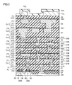
- FIG. 3 is a partial cross-sectional view schematically showing a configuration in an element formation region of FIG. 2.
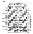
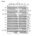
- FIG. 3 is a partial cross-sectional view schematically showing a configuration in a guard ring region of FIG. 2.
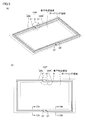
- FIGS. 2A and 2B are a perspective view and a plan view schematically showing the configuration of the guard ring of the semiconductor device in the first embodiment.
- FIGS. FIG. 5B is a schematic cross-sectional view along the VIA-VIA line (A), a schematic cross-sectional view along the VIB-VIB line in FIG.
- FIG. 6C is a schematic view (C) for explaining a deviation between a cross-sectional configuration along the line VIB-VIB in FIG.
- FIG. 5 is a schematic cross sectional view for illustrating a minimum dimension of a width of a guard ring conductive layer in the semiconductor device in the first embodiment.
- 6 is a schematic plan view showing a first exposure step of divided exposure in the method for manufacturing a semiconductor device in the first embodiment.
- FIG. FIG. 10 is a schematic plan view showing a second exposure step of divided exposure in the method for manufacturing a semiconductor device in the first embodiment.
- FIG. 10C is a sectional view (C) corresponding to a section taken along line XC-XC in the guard ring region of FIG.
- FIG. 10C is a sectional view (C) corresponding to a section taken along line XC-XC in the guard ring region of FIG.
- FIG. 10C is a sectional view (C) corresponding to a section taken along line XC-XC in the guard ring region of FIG.
- FIG. 10C is a sectional view (C) corresponding to a section taken along line XC-XC in the guard ring region of FIG. Sectional view (A) of the element formation region in the fifth step of the manufacturing method of the semiconductor device in the first embodiment, and a sectional view (B) corresponding to the section along the XB-XB line of the guard ring region of FIG.
- FIG. 10C is a sectional view (C) corresponding to a section taken along line XC-XC in the guard ring region of FIG.
- FIG. 10C is a sectional view (C) corresponding to a section taken along line XC-XC in the guard ring region of FIG.
- FIG. 10C is a sectional view (C) corresponding to a section taken along line XC-XC in the guard ring region of FIG.
- FIG. 10C is a sectional view (C) corresponding to a section taken along line XC-XC in the guard ring region of FIG.
- FIG. 10C is a sectional view (C) corresponding to a section taken along line XC-XC in the guard ring region of FIG. Sectional view (A) of the element formation region in the tenth step of the manufacturing method of the semiconductor device in the first embodiment, and a sectional view (B) corresponding to the section along the XB-XB line of the guard ring region of FIG.
- FIG. 10C is a sectional view (C) corresponding to a section taken along line XC-XC in the guard ring region of FIG.
- FIG. 10C is a sectional view (C) corresponding to a section taken along line XC-XC in the guard ring region of FIG.
- FIG. 10C is a sectional view (C) corresponding to a section taken along line XC-XC in the guard ring region of FIG.
- FIG. 10C is a sectional view (C) corresponding to a section taken along line XC-XC in the guard ring region of FIG.
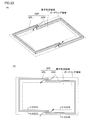
- They are a perspective view (A) and a plan view (B) schematically showing a configuration of a guard ring of a semiconductor device in a comparative example.
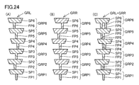
- FIG. 23B is a schematic cross-sectional view corresponding to the cross section along the line XXIVA-XXIVA in FIG. 23B
- FIG. 23B is a schematic cross-sectional view corresponding to the cross section along the line XXIVB-XXIVB in FIG.
- FIG. 24C is a schematic diagram (C) for explaining a deviation between a cross-sectional configuration corresponding to a cross section taken along line XXIVA-XXIVA in (B) and a cross-sectional configuration corresponding to a cross section taken along line XXIVB-XXIVB in FIG.
- FIG. 10 is a partial cross sectional view schematically showing a configuration of a modified example in the guard ring region of the semiconductor device in the first embodiment.
- FIG. 10 is a partial cross sectional view schematically showing a configuration of a modified example in the guard ring region of the semiconductor device in the first embodiment.
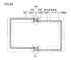
- FIG. 6 is a plan view schematically showing a configuration of a guard ring of a semiconductor device in a second embodiment. It is a schematic plan view which expands and shows the structure of the area
- FIG. 27 is a schematic plan view showing a first modification of the configuration of the region P2 in FIG. 26 in an enlarged manner. It is a schematic plan view which expands and shows the 2nd modification of the structure of the area
- FIG. 38 is a plan view schematically showing an eighteenth modification of the configuration of the guard ring of the semiconductor device in the second embodiment. It is a schematic plan view which expands and shows the structure of the area
- the semiconductor device of the present embodiment is, for example, a semiconductor chip or a semiconductor wafer of a CMOS sensor, but is not limited to this.
- the semiconductor device of this embodiment is a semiconductor chip of a CMOS sensor will be described as an example.
- the semiconductor chip SC of the CMOS sensor of the present embodiment has an element formation region, a guard ring region, and a scribe region in plan view (as viewed from the direction orthogonal to the main surface of the semiconductor substrate).
- the guard ring region is formed so as to surround the outer periphery (periphery) of the element formation region.
- the scribe region is formed so as to surround the outer periphery (periphery) of the guard ring region.
- the scribe area is an area for scribing when a semiconductor chip is cut out from the semiconductor wafer. For this reason, it may not remain on the outer periphery of the guard ring region depending on the method of scribing.
- the element formation region has a rectangular planar shape, for example.
- a pixel region PX a gain variable amplifier PGA, an analog-digital conversion circuit ADC, a timing generation circuit TG, a pixel driver VSCAN, a synchronization signal addition circuit BRIDGE, and an output driver LVDS are mainly used. Is formed.
- a guard ring GR is formed in the guard ring region.
- the guard ring GR extends in the guard ring region so as to surround the outer periphery of the element forming region having a rectangular planar shape.
- the guard ring GR serves to prevent moisture (humidity) from entering the element forming region on the inner peripheral side of the element forming region from the outer peripheral side.
- the semiconductor chip SC is a semiconductor device formed by divided exposure. Specifically, for example, a pattern of a region surrounded by a one-dot chain line MA is formed by exposure using a first photomask, and a pattern of a region surrounded by a one-dot chain line MB is defined as the first photomask. Are formed by exposure using a different second photomask.
- element isolation structure IR made of, for example, STI (Shallow Trench Isolation) or LOCOS (Local Oxidation of Silicon) oxide film is formed on the surface of semiconductor substrate SB made of, for example, silicon.
- An element such as a MOS (Metal Oxide Semiconductor) transistor TRA is formed in the element formation region on the surface of the semiconductor substrate SB electrically isolated by the element isolation structure IR. Each element formed in the element formation region is configured by the MOS transistor TRA and the like.
- each of the multilayer conductive layers CL and each of the multilayer interlayer insulating films II are alternately stacked.
- Each of the multilayer conductive layers CL is made of a material containing, for example, Cu (copper) and has a damascene structure.
- Each of the multilayer interlayer insulating films II is made of, for example, a silicon oxide film, a low dielectric constant (Low-k) material, or the like.
- the guard ring GR is constituted by a multilayer conductive layer CL in the guard ring region.
- Each of the multi-layered conductive layers CL constituting the guard ring GR is formed so as to surround the entire periphery of the element formation region in plan view.
- Each surface of the multilayer interlayer insulating film II is flattened, and has a relatively flat surface.
- An uppermost conductive layer TCL made of a material containing, for example, Al (aluminum) or Cu is formed on the uppermost interlayer insulating film II of the multilayered interlayer insulating film II.
- the uppermost conductive layer TCL includes a pad uppermost conductive layer TCL and a guard ring uppermost conductive layer TCL.
- the pad uppermost conductive layer TCL has a portion (pad portion) that is formed in the element formation region and functions as a pad electrode.
- the uppermost conductive layer TCL for guard ring is formed in the guard ring region and constitutes a part of the guard ring GR.
- the pad uppermost conductive layer TCL and the guard ring uppermost conductive layer TCL are layers formed separately from the same layer.
- the guard ring GR includes a multilayer conductive layer CL and a guard ring uppermost conductive layer TCL. Since the guard ring GR is mainly for preventing moisture (humidity) from entering the element formation region, the guard ring GR extends from the surface of the semiconductor substrate SB to the uppermost interlayer insulating film II. Is preferred. Each of the multilayer conductive layer CL and the guard ring uppermost conductive layer TCL is formed so as to surround the entire periphery of the element formation region in plan view as shown in FIG.
- passivation film PAL is formed on uppermost interlayer insulating film II so as to cover uppermost conductive layer TCL for pad and uppermost conductive layer TCL for guard ring.
- the passivation film PAL is formed in each of the element formation region, the guard ring region, and the scribe region.
- the passivation film PAL is made of a material having moisture resistance, and is made of, for example, a single insulating film containing nitrogen or a laminated film containing an insulating film containing nitrogen.
- the passivation film PAL includes p-SiN (plasma silicon nitride film), p-SiON (plasma silicon oxynitride film), p-SiN / p-SiO 2 (plasma silicon nitride film / plasma silicon oxide film). , P-SiON / p-SiO 2 (plasma silicon oxynitride film / plasma silicon oxide film).
- an opening OP1 reaching the surface of the pad uppermost conductive layer TCL is formed in the passivation film PAL on the pad uppermost conductive layer TCL. A part of the surface of the pad uppermost conductive layer TCL is exposed from the passivation film PAL through the opening OP1.
- a silane slit SS is formed on the outermost peripheral side of the guard ring region.
- the silane slit SS is a groove that penetrates the passivation film PAL and reaches the uppermost interlayer insulating film II.
- the silane slit SS is formed so as to surround the entire circumference of the guard ring GR.
- the silane slit SS is for preventing cracks propagating in the passivation film PAL from extending into the guard ring GR and the element formation region when the semiconductor wafer is separated into semiconductor chips by dicing.
- a first photosensitive organic insulating film PO1 is formed on the passivation film PAL.
- the first photosensitive organic insulating film PO1 is made of polyimide, for example.
- an opening OP2 reaching the surface of the uppermost conductive layer TCL for pads is formed in the first photosensitive organic insulating film PO1.
- the opening OP2 is formed so as to pass through the inside of the opening OP1.
- a part of the surface of the uppermost conductive layer TCL for pads is exposed from the first photosensitive organic insulating film PO1 through the opening OP2.
- a rewiring layer RIL is formed on the first photosensitive organic insulating film PO1.
- the redistribution layer RIL is connected to the pad portion of the uppermost conductive layer TCL for pads through the opening OP2.
- the redistribution layer RIL is formed so as to extend from a region directly above the pad portion of the uppermost conductive layer TCL for pads to a region other than the region directly above.
- This redistribution layer RIL has a barrier metal layer BM formed in contact with the surface of the first photosensitive organic insulating film PO1, and a conductive layer DCL formed on the barrier metal layer BM.
- the barrier metal layer BM is made of, for example, one of Cr (chromium), Ti (titanium), TiN (titanium nitride), Ta (tantalum), W (tungsten), Mo (molybdenum), or any combination thereof. It is made of a material that contains it.
- Conductive layer DCL is made of a material containing Cu, for example.
- a second photosensitive organic insulating film PO2 is formed on the first photosensitive organic insulating film PO1 so as to cover the rewiring layer RIL.
- the second photosensitive organic insulating film PO2 is made of polyimide, for example.
- An opening OP3 reaching the surface of the rewiring layer RIL is formed in the second photosensitive organic insulating film PO2. A part of the surface of the rewiring layer RIL is exposed from the second photosensitive organic insulating film PO2 through the opening OP3.
- Bump electrodes BP are formed on the second photosensitive organic insulating film PO2 so as to be connected to the rewiring layer RIL through the opening OP3.
- the bump electrode BP is electrically connected to the uppermost conductive layer TCL for pads through the rewiring layer RIL.
- the bump electrode BP is located immediately above the other region other than the region directly above the pad portion of the pad uppermost conductive layer TCL.
- the bump electrode BP has an alloy composition of, for example, Sn (tin) -xAg (silver) -0.5Cu.
- a multilayer wiring structure is constituted by conductive layers CL1 to CL7.
- This multilayer wiring structure is for electrically connecting the elements formed on the semiconductor substrate SB and electrically connecting the elements to the outside through the bump electrodes BP (FIG. 2).
- the MOS transistor TRA as an element formed on the semiconductor substrate has a pair of source / drain regions SD and a gate electrode GE.
- the pair of source / drain regions SD are formed on the surface of the semiconductor substrate SB so as to be spaced from each other.
- the gate electrode GE is formed on the surface of the semiconductor substrate SB sandwiched between the pair of source / drain regions SD with the gate insulating layer GI interposed therebetween.
- An etching stopper insulating film ES and an interlayer insulating film II1 are laminated on the surface of the semiconductor substrate SB so as to cover the MOS transistor TRA and the like.
- a contact hole CH and a wiring trench IT are formed in these insulating films ES and II1.
- the contact hole CH is formed so as to reach the gate electrode GE and the impurity region.
- the wiring trench IT is formed so as to communicate with the contact hole CH on the contact hole CH.
- a plug conductive layer PL is embedded in the contact hole CH, and a wiring conductive layer IL is formed in the wiring groove IT.
- the insulating film BL1 and the interlayer insulating film II2 are stacked on the interlayer insulating film II1.
- a via hole VH1 and a wiring trench IT1 are formed in these insulating films BL1 and II2.
- the via hole VH1 is formed so as to reach the wiring conductive layer IL.
- the wiring trench IT1 is formed on the via hole VH1 so as to communicate with the via hole VH1.
- a wiring conductive layer CL1 is formed in the via hole VH1 and the wiring groove IT.
- the wiring conductive layer CL1 has a portion PL1 formed in the via hole VH1 and a portion IL1 formed in the wiring trench IT1.
- the insulating film BL8 and the interlayer insulating film II9 are stacked on the interlayer insulating film II8.
- a via hole VH8 is formed in these insulating films BL8 and II9, and a plug conductive layer PL is formed in the via hole VH8.
- the uppermost conductive layer TCL formed on the interlayer insulating film II9 is electrically connected to the wiring conductive layer CL7 through the plug conductive layer PL.
- guard ring conductive layers GRP1 to GRP8 are formed by laminating each other. Although only one row of guard ring conductive layers GRP1 to GRP8 is shown in FIG. 4, a plurality of rows (eg, three rows) of guard ring conductive layers may be formed as shown in FIG. .
- the etching stopper insulating film ES and the interlayer insulating film II1 are stacked.
- a guard ring hole GH1 is formed.
- the guard ring hole GH1 is formed so as to surround the entire periphery of the element formation region in plan view, and includes a first hole portion FH1 and a second hole portion SH1.
- the first hole portion FH1 is formed so as to reach the surface of the semiconductor substrate SB.
- the second hole portion SH1 is located on the first hole portion FH1 so as to communicate with the first hole portion FH1, and has a width larger than the width of the first hole portion FH1.
- a first portion FP1 of the guard ring conductive layer GRP1 is formed in the first hole portion FH1, and a second portion SP1 of the guard ring conductive layer GRP1 is formed in the second hole portion SH1. Has been.
- the insulating film BL1 and the interlayer insulating film II2 are stacked on the interlayer insulating film II1.
- a guard ring hole GH2 is formed in these insulating films BL1 and II2, a guard ring hole GH2 is formed.
- the guard ring hole GH2 is formed so as to surround the entire periphery of the element formation region in plan view, and has a first hole portion FH2 and a second hole portion SH2.
- the first hole portion FH2 is formed so as to reach the surface of the guard ring conductive layer GRP1.
- the second hole portion SH2 is positioned on the first hole portion FH2 so as to communicate with the first hole portion FH2, and has a width larger than the width D1A of the first hole portion FH2.
- a first portion FP2 of the guard ring conductive layer GRP2 is formed in the first hole portion FH2, and a second portion SP2 of the guard ring conductive layer GRP2 is formed in the second hole portion SH2. Has been. Thus, the guard ring conductive layer GRP2 is connected to the guard ring conductive layer GRP1.
- a plurality of guard ring conductive layers GRP3 to GRP1 laminated in the vertical direction constitute a guard ring laminate.
- the insulating film BL8 and the interlayer insulating film II9 are stacked on the interlayer insulating film II8.
- a guard ring hole GH9 is formed in these insulating films BL8 and II9, and a plug conductive layer PL is formed in the guard ring hole GH9.
- the uppermost conductive layer TCL formed on the interlayer insulating film II9 is electrically connected to the guard ring conductive layer GRP8 via the plug conductive layer PL.
- guard ring GR including the plurality of guard ring conductive layers GRP1 to GRP8 and the uppermost conductive layer TCL is configured.
- interlayer insulating films II1 to II9 having the same reference numerals in the element formation region (FIG. 3) and the guard ring region (FIG. 4) are made of the same layer.
- the insulating films ES and BL1 to BL8 having the same reference numerals in the element formation region (FIG. 3) and the guard ring region (FIG. 4) are made of the same layer.
- the conductive layer for wiring and the conductive layer for guard ring formed in the same interlayer insulating film in the element formation region (FIG. 3) and the guard ring region (FIG. 4) were formed separately from the same conductive layer. Is.
- the wiring conductive layers CL2 to CL5 and the guard ring conductive layer GRP3 formed in the same interlayer insulating film II3 to II6 in the element formation region (FIG. 3) and the guard ring region (FIG. 4).
- the minimum widths D2A to D5A of the guard ring conductive layers GRP3 to GRP6 are larger than the minimum widths D2B to D5B of the conductive layers CL2 to CL5 for wiring.
- the width of the guard ring conductive layers GRP3 to GRP6 is a width in a cross section orthogonal to the direction in which the guard ring GR extends.
- the width of the wiring conductive layers CL2 to CL5 is a width in a cross section orthogonal to the direction in which each of the wiring conductive layers CL2 to CL5 extends.
- the minimum width D2A of the guard ring conductive layer GRP3 is larger than the minimum width D2B of the wiring conductive layer CL2.
- the minimum width D3A of the guard ring conductive layer GRP4 is larger than the minimum width D3B of the wiring conductive layer CL3.
- the minimum width D4A of the guard ring conductive layer GRP5 is larger than the minimum width D4B of the wiring conductive layer CL4.
- the minimum width D5A of the guard ring conductive layer GRP6 is larger than the minimum width D5B of the wiring conductive layer CL5.
- each of the minimum dimensions D2B to D5B of the width of the wiring conductive layers CL2 to CL5 is, for example, 90 nm.
- the minimum width D2A of the guard ring conductive layer GRP3 is, for example, 110 nm.
- the minimum width D3A of the guard ring conductive layer GRP4 is, for example, 130 nm.
- the minimum width D4A of the guard ring conductive layer GRP5 is, for example, 150 nm.
- the minimum width D5A of the guard ring conductive layer GRP6 is, for example, 170 nm.
- the minimum dimension of the width of each of the plurality of guard ring conductive layers GRP2 to GRP6 is larger as the guard ring conductive layer on the upper layer side.
- the minimum width dimension D2A of the guard ring conductive layer GRP3 is larger than the minimum width dimension D1A of the guard ring conductive layer GRP2.
- the minimum width D3A of the guard ring conductive layer GRP4 is larger than the minimum width D2A of the guard ring conductive layer GRP3.
- the minimum width D4A of the guard ring conductive layer GRP5 is larger than the minimum width D3A of the guard ring conductive layer GRP4.
- the minimum width D5A of the guard ring conductive layer GRP6 is larger than the minimum width D4A of the guard ring conductive layer GRP5.
- the minimum dimensions D1A, D2A, D3A, D4A, and D5A of the widths of the guard ring conductive layers GRP2, GRP3, GRP4, GRP5, and GRP6 are, for example, 90 nm, 110 nm, 130 nm, 150 nm, and 170 nm, respectively.
- the minimum dimensions D1A to D5A of the respective widths of the guard ring conductive layers GRP3 to GRP6 may be in the range of 100 nm to 1000 nm.
- the widths of the plurality of guard ring conductive layers GRP2 to GRP6 may be the same.
- each of the first portions FP2 to FP6 embedded in the first hole portions FH2 to FH6 of the conductive layers GRP2 to GRP6 for the guard rings is usually as shown by taking the first portion FP6 as an example in FIG.
- the cross-sectional shape has a tapered shape in which the size is reduced toward the lower side.
- the minimum width dimensions D1A to D5A of the guard ring conductive layers GRP2 to GRP6 are the widths of the lowermost ends of the first portions FP2 to FP6.
- the minimum width D1A to D5A of each of the plurality of guard ring conductive layers GRP2 to GRP6 is the overlap of the photomask in forming each guard ring conductive layer GRP2 to GRP6. It is larger than the amount of deviation.
- the minimum width D1A to D5A of each of the plurality of guard ring conductive layers GRP2 to GRP6 is the amount of misalignment of the photomask when the respective guard ring conductive layers GRP2 to GRP6 are formed. It is preferably 1.2 times or more and 10 times or less.
- the overlay deviation amount of the photomask of the guard ring conductive layer GRP3 is, for example, 100 nm, and the minimum dimension D2A of the width of the guard ring conductive layer GRP3 is, for example, 110 nm.
- the overlay deviation amount of the photomask of the guard ring conductive layer GRP4 is, for example, 120 nm, and the minimum dimension D3A of the width of the guard ring conductive layer GRP4 is, for example, 130 nm.
- the amount of misalignment of the photomask in the guard ring conductive layer GRP5 is, for example, 140 nm, and the minimum width D4A of the guard ring conductive layer GRP5 is, for example, 150 nm.
- the amount of misalignment of the photomask of the guard ring conductive layer GRP6 is 160 nm, for example, and the minimum dimension D5A of the width of the guard ring conductive layer GRP 6 is 170 nm, for example. Note that the amount of misalignment of the photomask usually increases toward the upper layer.
- each guard ring conductive layer GRP (GRP2 to GRP6) is formed by divided exposure. Therefore, the first pattern portion GRL (the left portion in the figure) of the guard ring conductive layer GRP formed by exposure using the first photomask and the exposure using the second photomask are formed. There may be a positional deviation between the second pattern portion GRR (the right portion in the drawing) of the guard ring conductive layer GRP.
- the connection between the first pattern portion GRL and the second pattern portion GRR is maintained.
- each of the guard ring conductive layers GRP1 to GRP6 formed by stacking in the first pattern portion GRL is displaced from each other (FIG. 6A). (Shifted in the middle / left / right direction).
- each of the guard ring conductive layers GRP1 to GRP6 formed by stacking each other is shifted from each other due to the overlay shift of the photomask ( (Shifted in the horizontal direction in the figure).
- the guard ring conductive layer in the first pattern portion GRL is formed.
- Each of GPR1 to GPR6 and each of the guard ring conductive layers GPR1 to GPR6 in the second pattern portion GRR are connected to each other, and no gap is generated between them.
- the remaining region EX2 (region surrounded by a two-dot chain line in FIG. 9) of one semiconductor chip region CHR is exposed using a second photomask.
- the entire semiconductor chip region CHR is exposed, and the exposure pattern in the exposure region EX1 and the exposure pattern in the exposure region EX2 are connected to each other.
- the photoresist (not shown) subjected to the above exposure is developed to form a resist pattern.
- the photoresist (not shown) subjected to the above exposure is developed to form a resist pattern.
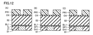
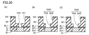
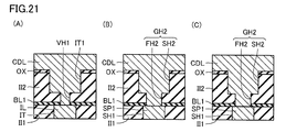
- FIGS. 10 (A) to 22 (A) show a partial cross section in the element formation region exposed by the first photomask shown in FIGS. 8 and 9.
- FIG. FIGS. 10B to 22B show cross sections corresponding to the cross section along the XB-XB line in the guard ring region exposed by the first photomask shown in FIGS. Yes.
- FIGS. 10C to 22C show cross sections corresponding to the cross section of the portion along the XC-XC line in the guard ring region exposed by the second photomask shown in FIG.
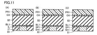
- an insulating film BL1 made of, for example, SiCO or SiCN and an interlayer insulating film II2 made of, for example, a low-k film are sequentially stacked on the interlayer insulating film II1. It is formed. Thereafter, a silicon oxide film OX is formed on the interlayer insulating film II2, and a photoresist PR1 is applied on the silicon oxide film OX. Divided exposure using the first photomask shown in FIG. 8 is performed on this photoresist PR1. As a result, an exposed region and a non-exposed region are generated with the broken line shown in the photoresist PR1 in FIGS. 10A and 10B as a boundary. On the other hand, the photoresist PR1 shown in FIG. 10C is not exposed using the first photomask.
- the photoresist PR1 is subjected to divided exposure using the second photomask shown in FIG. As a result, an exposed region and a non-exposed region are generated with the broken line shown in the photoresist PR1 in FIG. Thereafter, the photoresist PR1 is developed.
- the photoresist PR1 is patterned by the above development to form a resist pattern PR1.
- anisotropic etching is performed on the lower silicon oxide film OX and the interlayer insulating film II2.
- the silicon oxide film OX and the interlayer insulating film II2 are selectively removed by the above etching, and holes VH1 and FH2 reaching the insulating film BL1 are formed. At this time, the hole FH2 is formed so that the width thereof is larger than the width of the hole VH1. Thereafter, resist pattern PR1 is removed by, for example, ashing.
- the surface of silicon oxide film OX is exposed by removing resist pattern PR1.
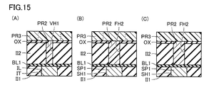
- each of holes VH1 and FH2 is filled with photoresist PR2.
- a photoresist PR3 is applied on the silicon oxide film OX.
- Divided exposure using the first photomask shown in FIG. 8 is performed on this photoresist PR3.
- an exposed region and a non-exposed region are generated with the broken line shown in the photoresist PR3 in FIGS.
- the photoresist PR3 shown in FIG. 15C is not exposed using the first photomask.
- photoresist PR3 divided exposure using the second photomask shown in FIG. 9 is performed on photoresist PR3. As a result, an exposed region and a non-exposed region are generated with the broken line shown in the photoresist PR3 in FIG. Thereafter, the photoresist PR3 is developed.
- first and second photomasks used in the steps of FIGS. 15 and 16 have different patterns from the first and second photomasks used in the steps of FIGS.
- the photoresist PR3 is patterned by the above development to form a resist pattern PR3.
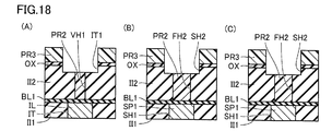
- anisotropic etching is performed on the lower silicon oxide film OX and the interlayer insulating film II2.
- trenches IT1 and SH2 are formed in interlayer insulating film II2 by the etching described above. Thereafter, resist patterns PR2 and PR3 are removed by, for example, ashing.
- the surface of silicon oxide film OX is exposed by the above ashing, and insulating film BL1 is exposed from each of holes VH1 and FH2.
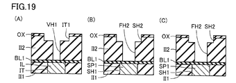
- anisotropic etching is performed on insulating film BL1 exposed from each of holes VH1 and FH2 using silicon oxide film OX and interlayer insulating film II2 as a mask.
- the insulating film BL1 is selectively removed, and a part of the surface of the wiring conductive layer IL and a part of the surface of the second part SP1 of the guard ring conductive layer GRP1 are exposed.
- the trenches IT1 and SH2 are formed deeply to form the wiring trench IT1 and the second hole portion SH2 of the guard ring hole GH2.
- the first hole portion FH2 and the second hole portion SH2 constitute a guard ring hole GH2.
- conductive layer CDL is formed on silicon oxide film OX so as to fill via hole VH1, wiring trench IT1, and guard ring hole GH2.
- Chemical mechanical polishing (CMP) is performed on the upper surface of the conductive layer CDL. This chemical mechanical polishing is performed until the surface of the interlayer insulating film II2 is exposed.
- Conductive layer GRP2 is formed.
- the minimum dimensions D1A to D5A of the respective widths of the guard ring conductive layers GRP2 to GRP6 and the minimum dimensions D1B to D5B of the respective widths of the conductive layers CL2 to CL5 for wiring are the same dimensions.
- the guard ring conductive layer is formed by divided exposure, a photomask overlay error occurs in the first pattern portion formed by the first photomask, and the second photomask is formed by the second photomask. Even in the pattern portion of 2, the photomask overlay shift occurs. Due to the overlay error, as shown in FIGS. 23 and 24, the first pattern portion and the second pattern portion of the conductive layer for the guard ring may not be connected, and a gap may be generated between them. When such a gap occurs, moisture (humidity) enters the element formation region on the inner peripheral side from the outer peripheral side of the guard ring through the gap along the path indicated by the arrow in FIGS. 23 (A) and (B). Reliability decreases.
- each of the minimum dimensions D2A to D5A of the width of the guard ring conductive layers GRP3 to GRP6 is a wiring conductive layer formed in the same interlayer insulating film as the guard ring conductive layer.
- the widths of the layers CL2 to CL5 are larger than each of the minimum dimensions D2B to D5B. For this reason, even if the first pattern portion GRL and the second pattern portion GRR of the guard ring conductive layer GRP are shifted from each other as shown in FIGS. 5A and 5B due to the mask overlay error in the divided exposure. The first pattern portion GRL and the second pattern portion GRR can be prevented from separating.
- the minimum width D1A to D5A of each of the plurality of guard ring conductive layers GRP2 to GRP6 is the overlap of the photomask in forming each guard ring conductive layer GRP2 to GRP6. It is preferable that the deviation amount is 1.2 times or more and 10 times or less. By making it 1.2 times or more, as shown in FIG. 5, it is possible to reliably prevent a gap from being generated between the first pattern portion GRL and the second pattern portion GRR of the guard ring conductive layer GRP. Can do. On the other hand, if it exceeds ten times, the dimensions D2A to D5A of the first portions FH3 to FH6 of the guard ring holes GH3 to GH6 become too large as shown in FIG. It becomes difficult to embed with.
- the amount of misalignment of the photomask increases as the upper layer.
- the guard ring conductive layer is formed by divided exposure, the upper guard ring conductive layer has a larger shift amount between the first pattern portion and the second pattern portion formed by the divided exposure, A gap is likely to be generated between both pattern portions.
- the minimum dimensions D1A to D5A of the respective widths of the plurality of guard ring conductive layers GRP2 to GRP6 are larger as the upper guard ring conductive layer. It has become. For this reason, even if the mask misalignment increases as the upper layer as described above, the gap between the first pattern portion and the second pattern portion formed by the divided exposure in the upper guard ring conductive layer is increased. It can suppress that a clearance gap arises in the.
- each of the guard ring conductive layers GRP2 to GRP6 has a first portion FP2 to FP6 and a second portion SP2 to SP6, and the width thereof is that of the interlayer insulating films II2 to II6.
- the side walls of the guard ring conductive layers GRP2 to GRP6 extend linearly, so that the width of each of the guard ring conductive layers GRP2 to GRP6 is continuous in the thickness direction of the interlayer insulating films II2 to II6. May change. That is, the wall surfaces of the guard ring holes GH2 to GH6 may extend linearly in the thickness direction of the interlayer insulating films II2 to II6 and pass through the interlayer insulating films II2 to II6.
- FIG. 25 is substantially the same as the configuration of FIGS. 1 to 5 described above, and therefore the same elements are denoted by the same reference numerals and description thereof is not repeated.
- the planar shape of the guard ring conductive layer may have an intersecting shape in order to suppress the formation of a gap between patterns formed by each exposure when the guard ring conductive layer is formed by divided exposure. .
- a guard ring conductive layer having a cross shape will be described below as a second embodiment.
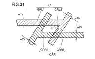
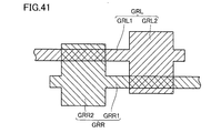
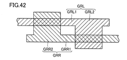
- guard ring conductive layers GRP (for example, guard ring conductive layers GRP2 to GRP6 shown in FIG. 4) of the present embodiment are formed by divided exposure. Therefore, the guard ring conductive layer GRP includes a first pattern portion GRL (left portion in the figure) of the guard ring conductive layer formed by exposure using the first photomask, and a second photo mask. And a second pattern portion GRR (a portion on the right side in the drawing) of the guard ring conductive layer formed by exposure using a mask.
- the first pattern part GRL has a frame part GRL1 and a bent part GRL2.
- Frame portion GRL1 surrounds the periphery of the element formation region (for example, the periphery of three sides of the rectangular element formation region) in plan view.
- the bent portion GRL2 is a portion that is connected to both ends of the frame portion GRL1 and is bent with respect to the frame portion GRL1.
- the bent portion GRL2 is connected so as to be bent at a right angle with respect to the frame portion GRL1, for example.
- the second pattern part GRR has a frame part GRR1 and a bent part GRR2 like the first pattern part GRL.
- Frame portion GRR1 surrounds the periphery of the element formation region (for example, the periphery of three sides of the rectangular element formation region) in plan view.
- the bent portion GRR2 is a portion that is connected to both ends of the frame portion GRR1 and is bent with respect to the frame portion GRR1.
- the bent portion GRR2 is connected so as to be bent, for example, at a right angle with respect to the frame portion GRR1.
- the width w1a of the frame part GRL1 and the width w1b of the bent part GRL2 in plan view are the same, for example.
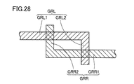
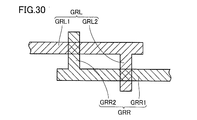
- the bent part GRL2 of the first pattern part GRL and the frame part GRR1 of the second pattern part GRR constitute an intersecting shape.
- the intersecting shape here means that the bent portion GRL2 and the frame portion GRR1 form a cross shape (a shape that intersects perpendicularly to each other) or an X shape (a shape that intersects each other obliquely) in plan view. ing.
- the crossing angle between the bent portion GRL2 and the frame portion GRR1 in plan view is, for example, 90 °, but may be greater than 0 ° and less than 180 °.
- the width w2a of the frame part GRR1 and the width w2b of the bent part GRR2 in plan view are the same, for example, but may be different.
- bent portion GRR2 of the second pattern portion GRR and the frame portion GRL1 of the first pattern portion GRL constitute an intersecting shape.
- the meaning of the intersection shape between the bent portion GRR2 and the frame portion GRL1 and the intersection angle are the same as those of the bent portion GRL2 and the frame portion GRR1.
- the guard ring conductive layer GRP has a narrow first portion FP2 to FP6 and a wide second portion SP2 to SP6 as shown in the guard ring conductive layers GRP2 to GRP6 in FIG.
- both the first portions FP2 to FP6 and the second portions SP2 to SP6 have the frame portions GRL1 and GRR1 and the bent portions GRL2 and GRR2.
- intersection shape in the present embodiment may be combined with the width of the guard ring conductive layer described in the first embodiment (such as a width larger than the width of the wiring conductive layer in the element formation region).
- the first pattern portion GRL and the second pattern portion GRR of the guard ring conductive layer intersect each other. For this reason, it can suppress that a clearance gap produces between a 1st pattern part and a 2nd pattern part by dividing exposure.
- FIGS. 28 to 30 are adopted as the configuration in which the frame part GRL1 (or GRR1) and the bent part GRL2 (or GRR2) have the same width and are orthogonal to each other. May be.
- the frame part GRL1 (or GRR1) and the bent part GRL2 (or GRR2) may have the same width as each other and may form an acute angle ⁇ 1.
- the frame part GRL1 (or GRR1) and the bent part GRL2 (or GRR2) may have the same width and may form an obtuse angle ⁇ 1.
- the frame part GRL1 (or GRR1) and the bent part GRL2 (or GRR2) may have different widths and may be orthogonal to each other.
- the width (w1b (or w2b): FIG. 39) of the bent portion GRL2 (or GRR2) is greater than the width (w1a (or w2a): FIG. 39) of the frame portion GRL1 (or GRR1).
- the width (w1b (or w2b)) of the bent part GRL2 (or GRR2) may be smaller than the width (w1a (or w2a)) of the frame part GRL1 (or GRR1).
- the frame part GRL1 (or GRR1) and the bent part GRL2 (or GRR2) may have different widths.
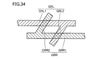
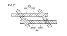
- the bent portion GRL2 (or GRR2) has a zigzag shape as shown in FIG. You may have, and you may have a lattice shape as shown in FIG.
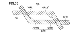
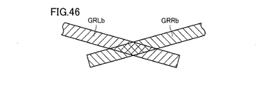
- the first pattern portion GRL has an obtuse angle with respect to each of the portion GRLa along one side of the rectangular planar shape of the element formation region and both ends of this portion GRLa.
- it has two inclined portions GRLb connected at an acute angle ⁇ 2.
- the second pattern portion GRR includes a portion GRRa along one side of the rectangular planar shape of the element formation region, and two slopes connected to each of both ends of the portion GRRa at an obtuse or acute angle ⁇ 2.
- Part GRRb Part GRRb.
- the inclined portion GRLb of the first pattern portion GRL and the inclined portion GRRb of the second pattern portion GRR intersect each other.
- the semiconductor device of the present embodiment may be, for example, a 35 mm full size sensor. Further, the semiconductor device of the present embodiment may be, for example, only the pixel portion of the 35 mm full size sensor or only the control circuit portion of the 35 mm full size sensor.
- the semiconductor chip includes, for example, a pixel PX, a timing generation circuit TG, a pixel driver VSCAN, and a gain variable amplifier PGA.
- the semiconductor chip includes, for example, an analog-digital conversion circuit ADC, a synchronization signal addition circuit BRIDGE, and an output driver LVDS.
Landscapes
- Internal Circuitry In Semiconductor Integrated Circuit Devices (AREA)
- Exposure And Positioning Against Photoresist Photosensitive Materials (AREA)
- Solid State Image Pick-Up Elements (AREA)
- Physics & Mathematics (AREA)
- Geometry (AREA)
- Engineering & Computer Science (AREA)
- Microelectronics & Electronic Packaging (AREA)
Abstract
Description
(実施の形態1)
まず本実施の形態の半導体装置の平面構成について図1を用いて説明する。
図2を参照して、たとえばシリコンよりなる半導体基板SBの表面には、たとえばSTI(Shallow Trench Isolation)またはLOCOS(Local Oxidation of Silicon)酸化膜よりなる素子分離構造IRが形成されている。この素子分離構造IRにより電気的に分離された半導体基板SBの表面であって、素子形成領域内には、たとえばMOS(Metal Oxide Semiconductor)トランジスタTRAなどの素子が形成されている。このMOSトランジスタTRAなどにより、上記の素子形成領域に形成された各素子が構成されている。
図8を参照して、分割露光においては、まず第1のフォトマスクを用いて1つの半導体チップ領域CHRの一部の領域EX1(図8中1点鎖線で囲んだ領域)のみが露光される。
ガードリング用導電層を分割露光で形成した場合の各露光で形成されるパターン間に隙間が生じることを抑制するために、ガードリング用導電層の平面形状が交差形状を有していてもよい。以下、交差形状を有するガードリング用導電層を実施の形態2として説明する。
Claims (9)
- 1つのチップ領域内に素子形成領域と、平面視において前記素子形成領域の周囲を取り囲むガードリング領域とを有し、かつ前記1つのチップ領域が分割露光により形成された半導体装置(SC)であって、
前記素子形成領域に形成されたビアホール(VH2~VH5)と前記ビアホール(VH2~VH5)上にて前記ビアホール(VH2~VH5)に連通する配線溝(IT2~IT5)とを有し、かつ前記ガードリング領域において前記素子形成領域を取り囲むように延在するガードリング用孔(GH3~GH6)を有する層間絶縁膜(II3~II6)と、
前記ビアホール(VH2~VH5)および前記配線溝(IT2~IT5)内に形成された部分を有する配線用導電層(CL2~CL5)と、
前記ガードリング用孔(GH3~GH6)内に形成された部分を有するガードリング用導電層(GRP3~GRP6)とを備え、
前記ガードリング用導電層(GRP3~GRP6)の幅の最小寸法(D2A~D5A)は、前記ビアホール(VH2~VH5)内における前記配線用導電層(CL2~CL5)の幅の最小寸法(D2B~D5B)よりも大きい、半導体装置。 - 前記ガードリング領域には、複数の前記ガードリング用導電層(GRP3~GRP6)を上下に互いに積層した構成を有するガードリング積層体が形成されており、
前記ガードリング積層体の複数の前記ガードリング用導電層(GRP3~GRP6)の各々の幅の最小寸法(D1A~D5A)は、上層側の前記ガードリング用導電層(GRP3~GRP6)ほど大きくなっている、請求項1に記載の半導体装置。 - 前記ガードリング用孔(GH3~GH6)は、第1の孔部(FH3~FH6)と、第2の孔部(SH3~SH6)とを有し、
前記第2の孔部(SH3~SH6)は、前記第1の孔部(FH3~FH6)上にて前記第1の孔部(FH3~FH6)に連通し、かつ前記第1の孔部(FH3~FH6)の幅よりも大きな幅を有し、
前記第1の孔部(FH3~FH6)内における前記ガードリング用導電層(GRP3~GRP6)の幅の最小寸法(D2A~D5A)が、前記ビアホール(VH2~VH5)内における前記配線用導電層(CL2~CL5)の幅の最小寸法(D2B~D5B)よりも大きい、請求項1に記載の半導体装置。 - 前記ガードリング用孔(GH3~GH6)の壁面は、前記ガードリング用孔(GH3~GH6)の延在方向に交差する断面において直線状に延びて前記層間絶縁膜(II3~II6)を貫通している、請求項1に記載の半導体装置。
- 素子形成領域と、前記素子形成領域の周囲を取り囲むガードリング領域とを1つのチップ領域に有し、前記1つのチップ領域が分割露光により形成された半導体装置(SC)であって、
前記ガードリング領域において前記素子形成領域を取り囲むように延在するガードリング用孔(GH3~GH6)を有する層間絶縁膜(II3~II6)と、
前記ガードリング用孔(GH3~GH6)内を埋め込むガードリング用導電層(GRP,GRP3~GRP6)とを備え、
前記ガードリング用導電層(GRP,GRP3~GRP6)は、平面視において互いに異なる方向に延びる第1および第2の部分(GRL1,GRL2,GRR1,GRR2)を有し、前記第1および第2の部分(GRL1,GRL2,GRR1,GRR2)が互いに交差する形状を有している、半導体装置。 - 平面視における前記第1および第2の部分(GRL1,GRL2,GRR1,GRR2)の交差角度は0°より大きく180°未満である、請求項5に記載の半導体装置。
- 前記第1および第2の部分(GRL1,GRL2,GRR1,GRR2)の線幅(w1a、w1b,w2a,w2b)が同じであり、前記第1および第2の部分(GRL1,GRL2,GRR1,GRR2)が互いに直交している、請求項6に記載の半導体装置。
- 前記第1および第2の部分(GRL1,GRL2,GRR1,GRR2)の線幅(w1a、w1b,w2a,w2b)が互いに異なっており、前記第1および第2の部分(GRL1,GRL2,GRR1,GRR2)が互いに直交している、請求項6に記載の半導体装置。
- 前記第1および第2の部分(GRL1,GRL2,GRR1,GRR2)が互いに斜めに交差している、請求項6に記載の半導体装置。
Priority Applications (7)
| Application Number | Priority Date | Filing Date | Title |
|---|---|---|---|
| CN201380070170.0A CN104919569B (zh) | 2013-01-11 | 2013-01-11 | 半导体装置 |
| JP2014556278A JP6117246B2 (ja) | 2013-01-11 | 2013-01-11 | 半導体装置およびその製造方法 |
| KR1020157021077A KR20150106420A (ko) | 2013-01-11 | 2013-01-11 | 반도체 장치 |
| US14/760,473 US9691719B2 (en) | 2013-01-11 | 2013-01-11 | Semiconductor device |
| PCT/JP2013/050369 WO2014109044A1 (ja) | 2013-01-11 | 2013-01-11 | 半導体装置 |
| TW102143651A TWI573238B (zh) | 2013-01-11 | 2013-11-29 | Semiconductor device |
| US15/602,290 US20170256506A1 (en) | 2013-01-11 | 2017-05-23 | Semiconductor device |
Applications Claiming Priority (1)
| Application Number | Priority Date | Filing Date | Title |
|---|---|---|---|
| PCT/JP2013/050369 WO2014109044A1 (ja) | 2013-01-11 | 2013-01-11 | 半導体装置 |
Related Child Applications (2)
| Application Number | Title | Priority Date | Filing Date |
|---|---|---|---|
| US14/760,473 A-371-Of-International US9691719B2 (en) | 2013-01-11 | 2013-01-11 | Semiconductor device |
| US15/602,290 Division US20170256506A1 (en) | 2013-01-11 | 2017-05-23 | Semiconductor device |
Publications (1)
| Publication Number | Publication Date |
|---|---|
| WO2014109044A1 true WO2014109044A1 (ja) | 2014-07-17 |
Family
ID=51166713
Family Applications (1)
| Application Number | Title | Priority Date | Filing Date |
|---|---|---|---|
| PCT/JP2013/050369 Ceased WO2014109044A1 (ja) | 2013-01-11 | 2013-01-11 | 半導体装置 |
Country Status (6)
| Country | Link |
|---|---|
| US (1) | US9691719B2 (ja) |
| JP (1) | JP6117246B2 (ja) |
| KR (1) | KR20150106420A (ja) |
| CN (1) | CN104919569B (ja) |
| TW (1) | TWI573238B (ja) |
| WO (1) | WO2014109044A1 (ja) |
Cited By (7)
| Publication number | Priority date | Publication date | Assignee | Title |
|---|---|---|---|---|
| JP2016051714A (ja) * | 2014-08-28 | 2016-04-11 | ルネサスエレクトロニクス株式会社 | 半導体装置およびその製造方法 |
| WO2018100974A1 (ja) * | 2016-11-30 | 2018-06-07 | 日東電工株式会社 | 配線回路基板およびその製造方法 |
| JP2019068265A (ja) * | 2017-09-29 | 2019-04-25 | キヤノン株式会社 | 半導体装置および機器 |
| US10332783B2 (en) | 2017-04-19 | 2019-06-25 | Canon Kabushiki Kaisha | Method of manufacturing semiconductor device, and semiconductor device |
| WO2021177026A1 (ja) * | 2020-03-05 | 2021-09-10 | ソニーセミコンダクタソリューションズ株式会社 | 固体撮像装置及び電子機器 |
| WO2025047553A1 (ja) * | 2023-08-30 | 2025-03-06 | ソニーセミコンダクタソリューションズ株式会社 | 半導体装置、電子機器及び半導体装置の製造方法 |
| DE102015215648B4 (de) | 2014-10-03 | 2026-04-23 | Mitsubishi Electric Corporation | Halbleitervorrichtung |
Families Citing this family (9)
| Publication number | Priority date | Publication date | Assignee | Title |
|---|---|---|---|---|
| CN104749846B (zh) * | 2015-04-17 | 2017-06-30 | 京东方科技集团股份有限公司 | 一种阵列基板及其制作方法、显示面板 |
| EP3355355B1 (en) * | 2017-01-27 | 2019-03-13 | Detection Technology Oy | Asymmetrically positioned guard ring contacts |
| KR102442096B1 (ko) * | 2017-11-22 | 2022-09-07 | 삼성전자주식회사 | 반도체 장치 |
| KR102497570B1 (ko) * | 2018-01-18 | 2023-02-10 | 삼성전자주식회사 | 반도체 장치 |
| JP6559841B1 (ja) * | 2018-06-01 | 2019-08-14 | エイブリック株式会社 | 半導体装置 |
| KR20210033581A (ko) * | 2019-09-18 | 2021-03-29 | 삼성디스플레이 주식회사 | 표시 장치 및 표시 장치의 제조 방법 |
| US11094650B1 (en) * | 2020-02-11 | 2021-08-17 | Taiwan Semiconductor Manufacturing Company Limited | Semiconductor arrangement and method of making |
| CN113053828B (zh) * | 2021-03-12 | 2022-05-27 | 长鑫存储技术有限公司 | 密封环及其形成方法 |
| TWI885271B (zh) * | 2022-06-21 | 2025-06-01 | 聯華電子股份有限公司 | 半導體結構 |
Citations (6)
| Publication number | Priority date | Publication date | Assignee | Title |
|---|---|---|---|---|
| JPH10199883A (ja) * | 1996-12-27 | 1998-07-31 | Lg Semicon Co Ltd | 半導体素子のガードリング並びにその形成方法 |
| JPH10335606A (ja) * | 1997-06-04 | 1998-12-18 | Matsushita Electron Corp | 半導体装置とその製造方法 |
| JP2002134506A (ja) * | 2000-10-19 | 2002-05-10 | Mitsubishi Electric Corp | 半導体装置 |
| JP2007227454A (ja) * | 2006-02-21 | 2007-09-06 | Toshiba Corp | 半導体装置の製造方法 |
| JP2008091893A (ja) * | 2006-09-06 | 2008-04-17 | Toshiba Corp | 半導体装置 |
| JP2012237933A (ja) * | 2011-05-13 | 2012-12-06 | Lapis Semiconductor Co Ltd | フォトマスク、露光方法、及び半導体装置の製造方法 |
Family Cites Families (28)
| Publication number | Priority date | Publication date | Assignee | Title |
|---|---|---|---|---|
| JPH05136020A (ja) * | 1991-11-11 | 1993-06-01 | Fujitsu Ltd | 半導体装置の露光方法 |
| JP3150461B2 (ja) * | 1992-12-17 | 2001-03-26 | 株式会社日立製作所 | 高集積電子回路装置とその製造方法 |
| US6022791A (en) * | 1997-10-15 | 2000-02-08 | International Business Machines Corporation | Chip crack stop |
| JP2002353307A (ja) * | 2001-05-25 | 2002-12-06 | Toshiba Corp | 半導体装置 |
| US6472740B1 (en) * | 2001-05-30 | 2002-10-29 | International Business Machines Corporation | Self-supporting air bridge interconnect structure for integrated circuits |
| JP3538170B2 (ja) * | 2001-09-11 | 2004-06-14 | 松下電器産業株式会社 | 半導体装置及びその製造方法 |
| JP2003249640A (ja) * | 2002-02-22 | 2003-09-05 | Sony Corp | 固体撮像素子の製造方法 |
| JP4250006B2 (ja) * | 2002-06-06 | 2009-04-08 | 富士通マイクロエレクトロニクス株式会社 | 半導体装置及びその製造方法 |
| JP3779243B2 (ja) * | 2002-07-31 | 2006-05-24 | 富士通株式会社 | 半導体装置及びその製造方法 |
| JP2004153115A (ja) * | 2002-10-31 | 2004-05-27 | Canon Inc | 半導体装置の製造方法 |
| JP4360881B2 (ja) | 2003-03-24 | 2009-11-11 | Necエレクトロニクス株式会社 | 多層配線を含む半導体装置およびその製造方法 |
| US7087452B2 (en) * | 2003-04-22 | 2006-08-08 | Intel Corporation | Edge arrangements for integrated circuit chips |
| JP2005072214A (ja) * | 2003-08-22 | 2005-03-17 | Semiconductor Leading Edge Technologies Inc | 荷電粒子線露光用マスク及び荷電粒子線露光方法 |
| JP2005129717A (ja) | 2003-10-23 | 2005-05-19 | Renesas Technology Corp | 半導体装置 |
| JP2005142262A (ja) | 2003-11-05 | 2005-06-02 | Toshiba Corp | 半導体装置および半導体装置の製造方法 |
| CN1617312A (zh) | 2003-11-10 | 2005-05-18 | 松下电器产业株式会社 | 半导体器件及其制造方法 |
| JP2005183600A (ja) * | 2003-12-18 | 2005-07-07 | Canon Inc | 半導体装置、固体撮像装置、増幅型固体撮像装置、撮像システム、マスク装置、及び露光装置 |
| JP2005209996A (ja) * | 2004-01-26 | 2005-08-04 | Semiconductor Leading Edge Technologies Inc | ステンシルマスク及び半導体装置の製造方法 |
| JP3890333B2 (ja) * | 2004-02-06 | 2007-03-07 | キヤノン株式会社 | 固体撮像装置 |
| JP4280204B2 (ja) * | 2004-06-15 | 2009-06-17 | Okiセミコンダクタ株式会社 | 半導体装置 |
| JP2006310446A (ja) | 2005-04-27 | 2006-11-09 | Canon Inc | 半導体装置の製造方法、および露光装置 |
| JP4699172B2 (ja) * | 2005-10-25 | 2011-06-08 | ルネサスエレクトロニクス株式会社 | 半導体装置 |
| US20080099884A1 (en) * | 2006-10-31 | 2008-05-01 | Masahio Inohara | Staggered guard ring structure |
| JP5220361B2 (ja) * | 2007-07-31 | 2013-06-26 | ルネサスエレクトロニクス株式会社 | 半導体ウエハおよび半導体装置の製造方法 |
| JP2009284424A (ja) * | 2008-05-26 | 2009-12-03 | Sony Corp | 撮像装置、撮像方法及びプログラム |
| JP5407422B2 (ja) | 2009-02-27 | 2014-02-05 | 富士通セミコンダクター株式会社 | 半導体装置及びその製造方法 |
| JP5792431B2 (ja) * | 2010-04-28 | 2015-10-14 | 日本電気株式会社 | 半導体装置の製造方法 |
| JP5849478B2 (ja) * | 2011-07-11 | 2016-01-27 | 富士通セミコンダクター株式会社 | 半導体装置および試験方法 |
-
2013
- 2013-01-11 WO PCT/JP2013/050369 patent/WO2014109044A1/ja not_active Ceased
- 2013-01-11 JP JP2014556278A patent/JP6117246B2/ja not_active Expired - Fee Related
- 2013-01-11 KR KR1020157021077A patent/KR20150106420A/ko not_active Ceased
- 2013-01-11 US US14/760,473 patent/US9691719B2/en active Active
- 2013-01-11 CN CN201380070170.0A patent/CN104919569B/zh not_active Expired - Fee Related
- 2013-11-29 TW TW102143651A patent/TWI573238B/zh not_active IP Right Cessation
Patent Citations (6)
| Publication number | Priority date | Publication date | Assignee | Title |
|---|---|---|---|---|
| JPH10199883A (ja) * | 1996-12-27 | 1998-07-31 | Lg Semicon Co Ltd | 半導体素子のガードリング並びにその形成方法 |
| JPH10335606A (ja) * | 1997-06-04 | 1998-12-18 | Matsushita Electron Corp | 半導体装置とその製造方法 |
| JP2002134506A (ja) * | 2000-10-19 | 2002-05-10 | Mitsubishi Electric Corp | 半導体装置 |
| JP2007227454A (ja) * | 2006-02-21 | 2007-09-06 | Toshiba Corp | 半導体装置の製造方法 |
| JP2008091893A (ja) * | 2006-09-06 | 2008-04-17 | Toshiba Corp | 半導体装置 |
| JP2012237933A (ja) * | 2011-05-13 | 2012-12-06 | Lapis Semiconductor Co Ltd | フォトマスク、露光方法、及び半導体装置の製造方法 |
Cited By (13)
| Publication number | Priority date | Publication date | Assignee | Title |
|---|---|---|---|---|
| JP2016051714A (ja) * | 2014-08-28 | 2016-04-11 | ルネサスエレクトロニクス株式会社 | 半導体装置およびその製造方法 |
| DE102015215648B4 (de) | 2014-10-03 | 2026-04-23 | Mitsubishi Electric Corporation | Halbleitervorrichtung |
| US11266024B2 (en) | 2016-11-30 | 2022-03-01 | Nitto Denko Corporation | Wired circuit board and production method thereof |
| WO2018100974A1 (ja) * | 2016-11-30 | 2018-06-07 | 日東電工株式会社 | 配線回路基板およびその製造方法 |
| JP2018092966A (ja) * | 2016-11-30 | 2018-06-14 | 日東電工株式会社 | 配線回路基板およびその製造方法 |
| US11032913B2 (en) | 2016-11-30 | 2021-06-08 | Nitto Denko Corporation | Wired circuit board and production method thereof |
| US10332783B2 (en) | 2017-04-19 | 2019-06-25 | Canon Kabushiki Kaisha | Method of manufacturing semiconductor device, and semiconductor device |
| JP2019068265A (ja) * | 2017-09-29 | 2019-04-25 | キヤノン株式会社 | 半導体装置および機器 |
| JP6991816B2 (ja) | 2017-09-29 | 2022-01-13 | キヤノン株式会社 | 半導体装置および機器 |
| JPWO2021177026A1 (ja) * | 2020-03-05 | 2021-09-10 | ||
| JP7728745B2 (ja) | 2020-03-05 | 2025-08-25 | ソニーセミコンダクタソリューションズ株式会社 | 固体撮像装置及び電子機器 |
| WO2021177026A1 (ja) * | 2020-03-05 | 2021-09-10 | ソニーセミコンダクタソリューションズ株式会社 | 固体撮像装置及び電子機器 |
| WO2025047553A1 (ja) * | 2023-08-30 | 2025-03-06 | ソニーセミコンダクタソリューションズ株式会社 | 半導体装置、電子機器及び半導体装置の製造方法 |
Also Published As
| Publication number | Publication date |
|---|---|
| TW201440190A (zh) | 2014-10-16 |
| JPWO2014109044A1 (ja) | 2017-01-19 |
| US20150357293A1 (en) | 2015-12-10 |
| JP6117246B2 (ja) | 2017-04-19 |
| CN104919569B (zh) | 2017-12-22 |
| KR20150106420A (ko) | 2015-09-21 |
| TWI573238B (zh) | 2017-03-01 |
| US9691719B2 (en) | 2017-06-27 |
| CN104919569A (zh) | 2015-09-16 |
Similar Documents
| Publication | Publication Date | Title |
|---|---|---|
| JP6117246B2 (ja) | 半導体装置およびその製造方法 | |
| KR102429310B1 (ko) | 반도체 장치 및 고체 촬상 소자 | |
| TWI650844B (zh) | 具有測試鍵結構的半導體晶圓 | |
| TWI650870B (zh) | 半導體裝置 | |
| US9117804B2 (en) | Interposer structure and manufacturing method thereof | |
| JP5326282B2 (ja) | 半導体装置とその製造方法、及び露光用マスク | |
| JP2009081351A (ja) | 半導体装置及びその製造方法 | |
| JP6180801B2 (ja) | 半導体装置 | |
| US20170256506A1 (en) | Semiconductor device | |
| JP6685653B2 (ja) | 固体撮像装置の製造方法 | |
| JP5493166B2 (ja) | 半導体装置及びその製造方法 | |
| JP2023055816A5 (ja) | ||
| US7843069B2 (en) | Wire bond pads | |
| TW202230701A (zh) | 半導體元件 | |
| JP2004111866A (ja) | 半導体装置の製造方法 | |
| US7291931B2 (en) | Semiconductor device, semiconductor substrate and fabrication process of a semiconductor device | |
| KR100577308B1 (ko) | 반도체 소자 및 그의 제조 방법 | |
| US10607942B2 (en) | Semiconductor device and method for manufacturing semiconductor device | |
| TWI843076B (zh) | 半導體裝置及其製造方法 | |
| JP5089194B2 (ja) | 半導体装置及びその製造方法 | |
| TW202103241A (zh) | 半導體元件及其製造方法 | |
| JP2014041928A (ja) | 半導体装置 | |
| CN111244072B (zh) | 半导体器件 | |
| TW202601768A (zh) | 晶圓結構及晶片結構 | |
| JP2010199185A (ja) | 半導体装置及びその製造方法 |
Legal Events
| Date | Code | Title | Description |
|---|---|---|---|
| 121 | Ep: the epo has been informed by wipo that ep was designated in this application |
Ref document number: 13870491 Country of ref document: EP Kind code of ref document: A1 |
|
| ENP | Entry into the national phase |
Ref document number: 2014556278 Country of ref document: JP Kind code of ref document: A |
|
| WWE | Wipo information: entry into national phase |
Ref document number: 14760473 Country of ref document: US |
|
| NENP | Non-entry into the national phase |
Ref country code: DE |
|
| ENP | Entry into the national phase |
Ref document number: 20157021077 Country of ref document: KR Kind code of ref document: A |
|
| 32PN | Ep: public notification in the ep bulletin as address of the adressee cannot be established |
Free format text: NOTING OF LOSS OF RIGHTS PURSUANT TO RULE 112(1) EPC (EPO FORM 1205 DATED 17-09-2015) |
|
| 122 | Ep: pct application non-entry in european phase |
Ref document number: 13870491 Country of ref document: EP Kind code of ref document: A1 |