WO2014097823A1 - 積層セラミック電子部品 - Google Patents
積層セラミック電子部品 Download PDFInfo
- Publication number
- WO2014097823A1 WO2014097823A1 PCT/JP2013/081569 JP2013081569W WO2014097823A1 WO 2014097823 A1 WO2014097823 A1 WO 2014097823A1 JP 2013081569 W JP2013081569 W JP 2013081569W WO 2014097823 A1 WO2014097823 A1 WO 2014097823A1
- Authority
- WO
- WIPO (PCT)
- Prior art keywords
- sample
- powder
- conductive layer
- experimental example
- multilayer ceramic
- Prior art date
- Legal status (The legal status is an assumption and is not a legal conclusion. Google has not performed a legal analysis and makes no representation as to the accuracy of the status listed.)
- Ceased
Links
Images

Classifications
-
- H—ELECTRICITY
- H01—ELECTRIC ELEMENTS
- H01G—CAPACITORS; CAPACITORS, RECTIFIERS, DETECTORS, SWITCHING DEVICES, LIGHT-SENSITIVE OR TEMPERATURE-SENSITIVE DEVICES OF THE ELECTROLYTIC TYPE
- H01G4/00—Fixed capacitors; Processes of their manufacture
- H01G4/002—Details
- H01G4/005—Electrodes
- H01G4/008—Selection of materials
-
- H—ELECTRICITY
- H01—ELECTRIC ELEMENTS
- H01G—CAPACITORS; CAPACITORS, RECTIFIERS, DETECTORS, SWITCHING DEVICES, LIGHT-SENSITIVE OR TEMPERATURE-SENSITIVE DEVICES OF THE ELECTROLYTIC TYPE
- H01G4/00—Fixed capacitors; Processes of their manufacture
- H01G4/30—Stacked capacitors
-
- H—ELECTRICITY
- H01—ELECTRIC ELEMENTS
- H01G—CAPACITORS; CAPACITORS, RECTIFIERS, DETECTORS, SWITCHING DEVICES, LIGHT-SENSITIVE OR TEMPERATURE-SENSITIVE DEVICES OF THE ELECTROLYTIC TYPE
- H01G4/00—Fixed capacitors; Processes of their manufacture
- H01G4/002—Details
- H01G4/005—Electrodes
- H01G4/012—Form of non-self-supporting electrodes
-
- H—ELECTRICITY
- H01—ELECTRIC ELEMENTS
- H01G—CAPACITORS; CAPACITORS, RECTIFIERS, DETECTORS, SWITCHING DEVICES, LIGHT-SENSITIVE OR TEMPERATURE-SENSITIVE DEVICES OF THE ELECTROLYTIC TYPE
- H01G4/00—Fixed capacitors; Processes of their manufacture
- H01G4/002—Details
- H01G4/228—Terminals
- H01G4/232—Terminals electrically connecting two or more layers of a stacked or rolled capacitor
-
- H—ELECTRICITY
- H01—ELECTRIC ELEMENTS
- H01G—CAPACITORS; CAPACITORS, RECTIFIERS, DETECTORS, SWITCHING DEVICES, LIGHT-SENSITIVE OR TEMPERATURE-SENSITIVE DEVICES OF THE ELECTROLYTIC TYPE
- H01G4/00—Fixed capacitors; Processes of their manufacture
- H01G4/002—Details
- H01G4/228—Terminals
- H01G4/232—Terminals electrically connecting two or more layers of a stacked or rolled capacitor
- H01G4/2325—Terminals electrically connecting two or more layers of a stacked or rolled capacitor characterised by the material of the terminals
-
- H—ELECTRICITY
- H01—ELECTRIC ELEMENTS
- H01G—CAPACITORS; CAPACITORS, RECTIFIERS, DETECTORS, SWITCHING DEVICES, LIGHT-SENSITIVE OR TEMPERATURE-SENSITIVE DEVICES OF THE ELECTROLYTIC TYPE
- H01G4/00—Fixed capacitors; Processes of their manufacture
- H01G4/002—Details
- H01G4/228—Terminals
- H01G4/248—Terminals the terminals embracing or surrounding the capacitive element, e.g. caps
-
- H—ELECTRICITY
- H01—ELECTRIC ELEMENTS
- H01G—CAPACITORS; CAPACITORS, RECTIFIERS, DETECTORS, SWITCHING DEVICES, LIGHT-SENSITIVE OR TEMPERATURE-SENSITIVE DEVICES OF THE ELECTROLYTIC TYPE
- H01G4/00—Fixed capacitors; Processes of their manufacture
- H01G4/002—Details
- H01G4/018—Dielectrics
- H01G4/06—Solid dielectrics
- H01G4/08—Inorganic dielectrics
- H01G4/12—Ceramic dielectrics
Definitions
- the present invention relates to a multilayer ceramic electronic component, and more particularly to a configuration of an external electrode.
- Patent Document 1 The technology that is of interest to the present invention is described in, for example, International Publication No. 2004/053901 pamphlet (Patent Document 1).
- Patent Document 1 is formed of a thermosetting conductive paste containing a metal powder (metal A) having a melting point of 300 ° C. or less, conductive particles having a high melting point (metal B), and a resin as described in claim 1.
- a multilayer ceramic electronic component having external electrodes is also described.
- Claim 2 stipulates that the total amount of A + B in the paste is 70 to 95% by weight with respect to the total amount of A + B + resin. The ratio is specified to be 5:95 to 20:80 by weight. Further, in the same claim 4, in order to obtain an external electrode, it is prescribed to hold at 80 to 400 ° C. for 1 to 60 minutes. In the same claim 5, the conductive particles in the external electrode and the metal of the internal electrode are specified. And are diffusion-bonded.
- Patent Document 1 stipulates that the blending ratio of the low melting point metal (A) is 5 to 20% by weight.
- a low melting point metal Since the ratio of A was as low as 5 to 20% by weight, it was found that the bondability with the internal electrode was poor. If the heat treatment is performed at 500 ° C. or more exceeding the range of 80 to 400 ° C. specified in claim 4, good bonding with the internal electrode is possible, but metal balls are deposited from the external electrode ( In other plating processes such as Ni plating that are performed thereafter, defective plating is caused.
- an object of the present invention is to provide a multilayer ceramic electronic component that can secure the electrical stability by solving the above-described problems and ensuring good bondability with respect to the internal electrode in the external electrode. Is to try.
- the present invention includes a laminate in which a ceramic layer and an internal electrode are laminated, and an external electrode formed on the outer surface of the laminate so as to be electrically connected to the internal electrode.
- the internal electrode includes a conductive layer that is in contact with the internal electrode, and the internal electrode is directed to a multilayer ceramic electronic component including Ni, and in order to solve the technical problem described above, the internal electrode and the conductive layer include: It is characterized by being bonded via a CuSnNi alloy phase.
- the amount of Ni solid solution in the CuSnNi alloy phase is 5 to 42 atm%.
- the conductive layer provided in the external electrode is in contact with the internal electrode via the CuSnNi alloy phase, a strong physical bonding is achieved between the external electrode and the internal electrode. It is possible to ensure the stability of the electrical characteristics of the electronic component.
- the CuSnNi alloy phase produced in the present invention has a lower temperature and a shorter time than the Ni 3 Sn 2 produced when an AgSn-based metal is used. Can be generated in
- the Ni solid solution amount in the CuSnNi alloy phase is selected in the range of 5 to 42 atm%, excessive diffusion of Ni between the internal electrode and the conductive layer is suppressed, and the external electrode and the internal electrode In this way, it is possible to more securely achieve a strong joint.
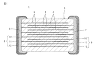
- FIG. 1 is a cross-sectional view showing a multilayer ceramic capacitor 1 according to an embodiment of the present invention.
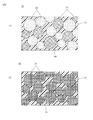
- FIG. 2 is a partially enlarged cross-sectional view of the conductive layer 10 schematically showing the formation process of the conductive layer 10 in the external electrodes 8 and 9 of the multilayer ceramic capacitor 1 shown in FIG. 1, wherein (1) is a state before heat treatment; 2) shows the state after heat treatment. It is a figure which shows the SEM photograph which image
- a multilayer ceramic capacitor 1 includes a multilayer body 5 in which a plurality of ceramic layers 2 made of a dielectric ceramic and a plurality of first and second internal electrodes 3 and 4 are laminated. .
- the first internal electrodes 3 and the second internal electrodes 4 are alternately arranged as viewed in the stacking direction, and the first internal electrodes 3 and the second internal electrodes 4 sandwich the ceramic layer 2.
- the first internal electrode 3 is drawn out to the first end face 6 of the multilayer body 5, and the second internal electrode 4 is drawn out to the second end face 7 facing the first end face 6 of the multilayer body 5. It is.
- the internal electrodes 3 and 4 contain Ni as a conductive component.
- the multilayer ceramic capacitor 1 also includes first and second external electrodes 8 and 9 formed on the outer surface of the multilayer body 5.
- the first external electrode 8 is formed so as to cover the first end face 6 of the multilayer body 5 and is electrically connected to the first internal electrode 3.
- the second external electrode 9 is formed so as to cover the second end face 7 of the multilayer body 5 and is electrically connected to the second internal electrode 4.
- Each of the external electrodes 8 and 9 includes a conductive layer 10 in contact with the outer surface of the multilayer body 5. Therefore, the conductive layers 10 of the first and second external electrodes 8 and 9 are in contact with the first and second internal electrodes 3 and 4, respectively.
- the detailed composition and forming method of the conductive layer 10 will be described later.
- the conductive layer 10 containing a resin has a single-layer structure, but a further conductive layer containing a resin may be formed on the conductive layer 10.
- each of the external electrodes 8 and 9 further includes a Ni plating layer 11 formed on the conductive layer 10 and a Sn plating layer 12 formed thereon.
- Ni and Sn constituting the plating layers 11 and 12 may be replaced with other metals such as Cu and Au as necessary. Further, either one of the plating layers 11 and 12 may be omitted. Furthermore, the plating layers 11 and 12 may not be formed, and the external electrodes 8 and 9 may be configured only by the conductive layer 10.
- thermosetting conductive resin composition containing Cu powder, Sn powder, a thermosetting resin, and an organic solvent is prepared.
- the content of Sn powder with respect to the total amount of Cu powder and Sn powder is preferably 36.5 to 47.8% by weight.
- the thermosetting resin contained in the thermosetting conductive resin composition is preferably selected so that the residual stress after curing is 8 MPa or more.
- thermosetting resin to be used is not particularly limited as long as the residual stress after curing satisfies 8 MPa or more.
- an epoxy resin is used as the main agent
- an alkaline resol type phenol resin or novolac type as the curing agent is used.
- the main epoxy resin is bisphenol A type epoxy resin, bisphenol F type epoxy resin, phenol novolac type epoxy resin, cresol novolac type epoxy resin, aromatic glycidylamine type epoxy resin, dimer acid modified epoxy resin, urethane modified
- An epoxy resin, a silicon-modified epoxy resin, a chelate-modified epoxy resin, an alicyclic epoxy resin, or a combination thereof can be used.
- thermosetting resin instead of a combination of an epoxy resin and a curing agent, a combination of an isocyanate compound and a polyol or an alkali resol type phenol resin exhibiting a self-polymerization reaction may be used alone as a thermosetting resin.
- thermosetting conductive resin composition described above is applied to the end faces 6 and 7 of the laminate 5 obtained through the firing process. More specifically, for example, by extending a paste-like uncured thermosetting conductive resin composition to a predetermined thickness with a squeegee and immersing each of the end faces 6 and 7 of the laminate 5 therein, An uncured thermosetting conductive resin composition is applied to the end faces 6 and 7 of the laminate 5. The applied thermosetting conductive resin composition is then dried to remove the organic solvent.
- FIG. 2 (1) schematically shows a cross-sectional structure of the thermosetting conductive resin composition 21 that should constitute the conductive layer 10 in a state after drying.
- the thermosetting conductive resin composition 21 is in a state where Cu powder 22 and Sn powder 23 are dispersed in the thermosetting resin 24. At least a part of each of the Cu powder 22 and the Sn powder 23 is in contact with each other.
- the total content of the Cu powder 22 and the Sn powder 23 in the dried thermosetting conductive resin composition 21 is preferably 45 to 65% by volume.
- the D50 of the Cu powder 22 contained in the thermosetting conductive resin composition before curing is 0.5 to 3.0 ⁇ m, and the D50 of the Sn powder 23 is 1.5 to 5.0 ⁇ m. preferable.
- thermosetting conductive resin composition 21 a heat treatment step of the thermosetting conductive resin composition 21 is performed.
- the above-described thermosetting resin 24 is cured, and mutual diffusion proceeds between the Cu powder 22 and the Sn powder 23.
- the thermosetting resin 24 is first cured, and the distance between the Cu powder 22 and the Sn powder 23 is shortened by curing shrinkage, and the contact increases. Subsequently, mutual diffusion proceeds between the Cu powder 22 and the Sn powder 23.
- FIG. 2 (2) a plurality of metal particles 25 containing a Cu 3 Sn alloy are generated.
- the thermosetting conductive resin composition 21 has a Sn powder 23 content of 36.5 to the total amount of the Cu powder 22 and the Sn powder 23.
- the metal component contained in the metal particles 25 shown in FIG. 2 (2) contains Cu and Sn, and the weight ratio of Sn to the total amount of Sn and Cu is 36.5 to 47.8%.
- the metal particles 25 may contain Cu 6 Sn 5 alloy, Cu 6 Sn 5 alloy, Cu metal and / or Sn metal in addition to Cu 3 Sn alloy. Further, as a result of mutual diffusion, holes may be left in a part of the portion where the Cu powder 22 or the Sn powder 23 is present in the thermosetting resin 24.
- the cured conductive layer 10 is formed.
- the deposition (or ejection) of the metal balls can be suppressed. It is presumed that Cu 3 Sn has a melting point of about 676 ° C. and does not remelt in the heat treatment process.
- FIG. 3 shows the “CuSnNi alloy phase” confirmed by the SEM photograph.
- a “CuSnNi alloy phase” is formed in a portion in contact with the “internal electrode” containing Ni and the conductive layer (portion where “Cu 3 Sn alloy” and “thermosetting resin” exist).
- the CuSnNi alloy phase shows an alloy composition of (Cu, Ni) 6 Sn 5 , and the composition varies depending on the solid solution amount of Ni.
- the amount of Ni solid solution in the alloy phase is preferably 5 to 42 atm%.
- the CuSnNi alloy phase contributes to the improvement of the bondability of the external electrodes 8 and 9 to the internal electrodes 3 and 4. It is presumed that the aforementioned Cu 3 Sn, which is an intermetallic compound that can be generated in the conductive layer 10, is metal-bonded to the internal electrodes 3 and 4 containing Ni, and as a result, a CuSnNi alloy phase is formed.
- the present invention has been described above in relation to the multilayer ceramic capacitor. However, the present invention can also be applied to multilayer ceramic electronic components other than the multilayer ceramic capacitor.
- thermosetting conductive resin composition Cu powder made of spherical particles with D50 of 1.0 ⁇ m, Sn powder made of spherical particles with D50 of 2.5 ⁇ m, and resol type phenol as a thermosetting resin Resin A and diethylene glycol monobutyl ether as an organic solvent were mixed with a small mixer and then kneaded with a three-metal roll. Then, while measuring the viscosity using an E-type viscometer, adjusting the amount of diethylene glycol monobutyl ether as an organic solvent to adjust the viscosity to 1 rpm / 30 ⁇ 2 Pa ⁇ s, an uncured thermosetting sample. Type conductive resin composition was obtained.
- the total content of Cu powder and Sn powder in the thermosetting conductive resin composition was 55% by volume, excluding the organic solvent, but Sn powder relative to the total amount of Sn powder and Cu powder.
- the ratio was changed as shown in the “Sn ratio” column of Table 1.
- the above D50 is a volume-based value measured by a laser diffraction method.
- thermosetting conductive resin composition prepared as described above is stretched to a thickness of 150 ⁇ m with a squeegee, and one end face of the laminate is immersed therein, thereby thermosetting conductive resin.
- the composition was applied, and then dried for 10 minutes at a temperature of 150 ° C. using a hot air circulating oven. Subsequently, the same process was implemented also about the other end surface of the laminated body. Thus, the laminated body to which the thermosetting conductive resin composition was provided to both end surfaces was obtained.
- the laminated body was heat-treated in a nitrogen atmosphere having an actually measured oxygen concentration of less than 10 ppm at a temperature rising rate of 15 ° C./min and kept at a top temperature of 450 ° C. for 20 minutes to obtain a thermosetting conductive
- the functional resin composition was cured.
- a laminated body in which the conductive layer in the external electrode was formed on both end surfaces was obtained.
- thermosetting conductive resin composition on the phosphor bronze plate was dried at a temperature of 150 ° C. for 10 minutes using a hot air drying oven, and then the temperature rising rate was 15 in a nitrogen atmosphere with an actually measured oxygen concentration of less than 10 ppm.
- the thermosetting conductive resin composition was cured by heating at a temperature of °C / min and heat treatment under the condition of keeping the top temperature at 450 ° C. for 20 minutes.
- the thickness of the cured resin film was measured with a micrometer, and the bending amount h of the phosphor bronze plate was measured by image analysis. Further, the Young's modulus of each of the cured resin film and phosphor bronze plate was measured with five samples using a micro hardness meter, and the average value was obtained. And the residual stress value after resin hardening was calculated
- the multilayer ceramic capacitor according to each sample was embedded in a resin and wet-polished to a position (W / 2 position) that was 1/2 of the width direction dimension. Using a SEM, the backscattered electron image was taken at a magnification of 1500 times.
- “x” is displayed in the “Jointability” column of Table 1, and all five CuSnNi alloy phases. Those that could be confirmed were marked with “ ⁇ ” in the same column.
- ⁇ indicates that the capacitance was all within ⁇ 20% of 1.0 ⁇ F, that is, in the range of 0.8 to 1.2 ⁇ F, in 20 samples. In addition, with respect to the dielectric loss tangent, all of the 20 samples were 7.5% or less.
- ⁇ (DF) indicates that the dielectric loss tangent was not higher than 15%, but even one piece was higher than 7.5%.
- the multilayer ceramic capacitor according to each sample is embedded in a resin and wet-polished to a position (W / 2 position) that is 1/2 of the width direction dimension, and then the entire cross section of the exposed conductive layer is subjected to energy dispersion X
- the intensity ratio of Cu and Sn was calculated
- EDX line analysis
- the obtained value coincided with the Sn powder content (“Sn ratio” in Table 1) of the thermosetting conductive resin composition before thermosetting.
- the “Ni ratio of the CuSnNi alloy phase” is not 0 atm%, that is, in the samples 2 to 7 in which the CuSnNi alloy phase is formed, each of the “metal balls”, “joinability”, and “electric properties” In the evaluation items, preferable results were obtained.
- the “Ni ratio of the CuSnNi alloy phase” is preferably 5 to 42 atm% for samples 2 to 6.
- the “residual stress after curing” obtained for the sample 4 showed a value of 10 MPa. From this, it can be inferred that the same “residual stress after curing” can be obtained for the other samples 1 to 3 and 5 to 7 which differ from the sample 4 only in the “Sn ratio”.
- thermosetting conductive resin composition An uncured thermosetting conductive resin composition having the same composition as Sample 4 in Experimental Example 1 was prepared.
- top temperature and the keep time for obtaining the sample 4-2 in Experimental Example 2 are the same as the top temperature and the keep time for obtaining the sample 4 in Experimental Example 1.
- the CuSnNi alloy phase between the internal electrode and the external electrode also tends to be difficult to form. Therefore, in the sample 4-5 in which the Cu 3 Sn alloy ratio is 15% by weight, the “joinability” was evaluated as “ ⁇ ”, but the formation ratio of the Cu 3 Sn alloy was lowered, which caused the CuSnNi alloy phase to be Only sparsely formed.
- the CuSnNi alloy phase can be sufficiently obtained. It can be estimated that it can be formed.
- thermosetting conductive resin composition (Experimental example with different thermosetting resin) (1) Preparation of thermosetting conductive resin composition The ratio of Sn powder to the total amount of Sn powder and Cu powder was fixed to 40% by weight. An uncured thermosetting conductive resin composition serving as a sample was obtained through the same operation as in Experimental Example 1 except that the resin shown in the “Type of resin” column was used.
- thermosetting resin not a resol type phenol resin but a combination of a polyfunctional epoxy resin and a novolac type phenol resin was used as the thermosetting resin. Comparing the sample 13 and the sample 14, as the thermosetting resin, the sample 13 uses a combination of a polyfunctional epoxy resin and a novolac type phenol resin D, and the sample 14 uses a polyfunctional epoxy resin and a novolac type phenol resin E. The combination with was used.
- thermosetting resin whose “residual stress after curing” can be 8 MPa or more.
- thermosetting conductive resin composition (Experimental example in which the metal content after drying was changed) (1) Preparation of thermosetting conductive resin composition The ratio of Sn powder to the total amount of Sn powder and Cu powder was fixed at 40 wt%, and instead, the organic solvent in the thermosetting conductive resin composition The total content of the Cu powder and the Sn powder excluding the sample, that is, the “metal content after drying” was changed as shown in Table 4, and the sample was subjected to the same operation as in Experimental Example 1. An uncured thermosetting conductive resin composition was obtained.
- sample 24 in the experimental example 4 is the same as the sample 4 in the experimental example 1.
- the “metal content after drying” is 40 vol%, 45 vol%, 50 vol%, 55 vol%, 60 vol%, 65 vol% and 70 vol%, respectively.
- Sample 21, Sample 22, Sample 23, Sample 24, Sample 25, Sample 26 and Sample 27 good results were obtained in all of “metal balls”, “joinability”, and “electric properties”.
- the sample 27 having a “metal content after drying” of 70% by volume does not cause a problem in terms of product characteristics. The denseness of was getting worse.
- the sample 21 having a “metal content after drying” of 40% by volume had no problem in terms of product characteristics, but the Ni plating property was deteriorated. This can be presumed to be due to the fact that the metal amount in the conductive layer is insufficient.
- the “metal content after drying” is preferably 45 to 65% by volume.
- thermosetting conductive resin composition (Experimental example in which D50 of Cu powder was changed) (1) Production of thermosetting conductive resin composition The ratio of Sn powder to the total amount of Sn powder and Cu powder was fixed at 40 wt%, and instead, “D50 of Cu powder” is shown in Table 5 Except for the change, the same operation as in Experimental Example 1 was performed to obtain an uncured thermosetting conductive resin composition as a sample.
- Sample 33 in Experimental Example 5 is the same as Sample 4 in Experimental Example 1.
- Example D31 in which “D50 of Cu powder” is 0.3 ⁇ m, 0.5 ⁇ m, 1.0 ⁇ m, 2.0 ⁇ m, 3.0 ⁇ m and 5.0 ⁇ m, respectively
- Sample 33, Sample 34, Sample 35, and Sample 36 good results were obtained in all of “metal balls”, “joinability”, and “electrical properties”.
- thermosetting conductive resin composition As the sample 31 with “Cu powder D50” of 0.3 ⁇ m, there is no problem in terms of product characteristics, but since the yield value of the paste of the thermosetting conductive resin composition is high, the thermosetting type When the conductive resin composition was applied to the laminate, it became a “horn” shape.
- “D50 of Cu powder” is preferably in the range of 0.5 to 3.0 ⁇ m.
- thermosetting conductive resin composition (Experimental example in which D50 of Sn powder was changed) (1) Production of thermosetting conductive resin composition The ratio of Sn powder to the total amount of Sn powder and Cu powder was fixed at 40 wt%, and instead, “D50 of Sn powder” is shown in Table 6 Except for the change, the same operation as in Experimental Example 1 was performed to obtain an uncured thermosetting conductive resin composition as a sample.
- sample 42 in the experimental example 6 is the same as the sample 4 in the experimental example 1.
- D50 of Sn powder is preferably in the range of 1.5 to 5.0 ⁇ m.
- thermosetting conductive resin composition (Experimental example with other conditions changed) (1) Preparation of thermosetting conductive resin composition The ratio of Sn powder to the total amount of Sn powder and Cu powder was fixed to 40 wt%. Instead, as shown in Table 7, in sample 51, "Cu An uncured thermosetting conductive resin composition serving as a sample was obtained through the same operation as in Experimental Example 1 except that the “powder shape” was flattened.
- thermosetting conductive resin composition according to Samples 52 and 53 in Experimental Example 7 is the same as the thermosetting conductive resin composition produced in Experimental Example 1.
- Sample 52 a laminate having a planar dimension of 1.6 mm ⁇ 0.8 mm was used as the laminate, as described in “1608” in the “laminate dimensions” column of Table 7.
- the plane size is 1.0 mm ⁇ 0.
- a laminate of 5 mm was used.
- thermosetting conductive resin composition As shown in the column of “Curing Top Temperature” in Table 7, the heat treatment top temperature for curing the thermosetting conductive resin composition was set to 400 ° C. In the other samples 51 and 52, as shown in the column of “curing top temperature” in Table 7, the heat treatment top temperature for curing the thermosetting conductive resin composition was set to 450 as in the case of Experimental Example 1. C.
- thermosetting conductive resin composition (Comparative Experimental Example of Sn Ratio) (1) Production of thermosetting conductive resin composition The ratio of Sn powder to the total amount of Sn powder and Cu powder is in the column of “Sn ratio” in Table 8 according to the ratio described in claim 3 of Patent Document 2. An uncured thermosetting conductive resin composition serving as a sample was obtained through the same operation as in Experimental Example 1 except that it was changed as shown in FIG.
- thermosetting conductive resin composition Formation of conductive layer As shown in the column of “curing top temperature” in Table 8, for samples 62 and 64, the heat treatment top temperature for curing the thermosetting conductive resin composition was 550 ° C. Except that, applying the same conditions as in Experimental Example 1 while applying a thermosetting conductive resin composition to both end faces of the laminate as a component body for a multilayer ceramic capacitor, and by heat treatment, A laminate in which conductive layers in the external electrode were formed on both end surfaces was obtained.
- the “curing top temperature” is, of course, the case of the samples 61 and 63 having a relatively low “curing top temperature” of 450 ° C. Even in the case of samples 62 and 64 having a comparatively high value of 550 ° C., “Jointability” was “x”, and “Electrical characteristics” was also evaluated as “x (cap / DF)”. The reason can be assumed to be because the absolute amount of Sn was insufficient.
- thermosetting conductive resin composition Ag powder was used instead of Cu powder, and the ratio of Sn powder to the total amount of Ag powder and Sn powder was defined in claim 3 of Patent Document 2.
- An uncured thermosetting conductive resin composition serving as a sample was obtained through the same operation as in Experimental Example 1 except that it was fixed at 20% by weight, which was the upper limit of the metal ratio on the low melting point side.
- thermosetting conductive resin composition is applied to both end faces of a laminate as a component body for a multilayer ceramic capacitor, and heat treatment is performed, so that a conductive layer in the external electrode is formed on both end faces. A formed laminate was obtained.
- the “curing top temperature” is 450 ° C.
- the “joinability” is “x”
- the “electrical property” is evaluated as “x (cap / DF)”.
- the “joinability” was “ ⁇ ”
- the “electrical property” was evaluated as “ ⁇ ”. It can be inferred that this is because the “curing top temperature” of 550 ° C. is higher than the melting point (481 ° C.) of the produced Ag 3 Sn and a liquid phase is produced.
- the “metal ball” becomes “NG”, which causes an appearance defect, and there is a concern about practical problems.
Landscapes
- Engineering & Computer Science (AREA)
- Power Engineering (AREA)
- Manufacturing & Machinery (AREA)
- Microelectronics & Electronic Packaging (AREA)
- Chemical & Material Sciences (AREA)
- Materials Engineering (AREA)
- Ceramic Capacitors (AREA)
- Fixed Capacitors And Capacitor Manufacturing Machines (AREA)
- Thermistors And Varistors (AREA)
- Ceramic Engineering (AREA)
- Inorganic Chemistry (AREA)
- Conductive Materials (AREA)
Abstract
Description
(1)熱硬化型導電性樹脂組成物の作製
D50が1.0μmの球状粒子からなるCu粉末と、D50が2.5μmの球状粒子からなるSn粉末と、熱硬化性樹脂としてのレゾール型フェノール樹脂Aと、有機溶剤としてのジエチレングリコールモノブチルエーテルとを、小型ミキサーで混合した後、金属3本ロールで混練した。その後、E型粘度計を用いて粘度測定しながら、有機溶剤としてのジエチレングリコールモノブチルエーテルの量を調整することによって、1rpm/30±2Pa・sに粘度調整された、試料となる未硬化の熱硬化型導電性樹脂組成物を得た。
Niを主成分とする内部電極が形成され、平面寸法が1.0mm×0.5mmであり、静電容量が1μFの積層セラミックコンデンサのための部品本体としての積層体を用意した。
次に、湿式電解バレル法を用いて、上記導通層上に、約2.5±1.5μmの厚みをもってNiめっき層を形成し、次いで、約3.5±1.5μmの厚みをもってSnめっき層を形成した。これによって、試料となる積層セラミックコンデンサを得た。
(4A)硬化後残留応力(リン青銅板法)
平面寸法が10mm×60mmで厚みが200μmのリン青銅板を用意し、このリン青銅板上に、試料となる熱硬化型導電性樹脂組成物を約150μmの厚みで塗布した。
ただし、
F(m,n)=((1-mn2)3×(1+m))+(mn(n+2)+1)3+m(mn2+2n+1)3)/(1+mn)3、 曲率半径ρ[mm]=(4x2+L2)/8x、
x=h/4、
h[mm]:リン青銅板湾曲量、
L[mm]:リン青銅板全長、
E1[GPa]:樹脂ヤング率、
E2[GPa]:リン青銅板ヤング率、
m=E1/E2、
h1[mm]:硬化した樹脂膜の厚み、
h2[mm]:リン青銅板厚み、
n=h1/h2
である。
外部電極における導通層が両端面に形成されためっき前の積層体を各試料につき5個準備し、積層体のいずれか一方の端面上の導通層の中央部を、電界放出型走査電子顕微鏡(FE-SEM)を用いて、二次電子像1000倍で観察した。積層体5個中、1個でも、径10μm以上の金属ボールの噴出が認められたものについては、表1の「金属ボール」の欄に「NG」と表示し、5個すべてで径10μm以上の金属ボールが認められなかったものについては、同欄に「G」と表示した。
試料としての積層セラミックコンデンサから、各試料につき5個の積層セラミックコンデンサを選出した。
上記(4C)において評価した試料について、積層方向での中央位置にある内部電極直上に生成したCuSnNi合金相を、エネルギー分散型X線分析(EDX)を用いて加速電圧10kVで点分析し、CuとSnとNiとの金属組成比を定量し、Ni固溶量を求め、5個の試料についてのNi固溶量の平均値を求めた。
各試料につき、20個の積層セラミックコンデンサを、150℃の温度で60分間熱処理した後、室温で24時間放置した。その後、LCRメータを用い、1MHz、0.5Vrmsの条件で、静電容量(cap)および誘電正接(DF)を測定した。
試料としての積層セラミックコンデンサから、各試料につき5個の積層セラミックコンデンサを選出した。
試料としての積層セラミックコンデンサから、各試料につき3個の積層セラミックコンデンサを選出した。次いで、各試料に係る積層セラミックコンデンサを樹脂包埋して、幅方向寸法の1/2の位置(W/2位置)まで湿式研磨したのち、露出した樹脂電極層の断面全体を、XRDを用いて分析することで、樹脂電極層内に含まれるCuとSnとCu3Sn合金とCu6Sn5合金の強度比を求めた。そして3個の試料についてCu3Sn合金比率の平均値を求めた。得られた値は表1の「Cu3Sn合金比率」の欄に示されている。

「CuSnNi合金相のNi比率」が0atm%ではない、すなわち、CuSnNi合金相が形成された試料2~7では、「金属ボール」、「接合性」、および「電気特性」の各評価項目において、好ましい結果が得られた。
(1)熱硬化型導電性樹脂組成物の作製
実験例1における試料4と同様の組成の未硬化の熱硬化型導電性樹脂組成物を作製した。
硬化時のトップ温度およびキープ時間を、表2の「硬化」における「トップ温度」および「キープ温度」にそれぞれ示すように変更したこと以外は、実験例1の場合と同様の操作を経て、外部電極における導通層が両端面に形成された積層体を得た。
実験例1の場合と同様の条件を適用しながら、導通層上に、Niめっき層およびSnめっき層を形成し、試料となる積層セラミックコンデンサを得た。
表2に示すように、各試料について、実験例1の場合と同様の要領で、「金属ボール」、「接合性」、「Cu3Sn合金比率」、および「電気特性」を評価した。
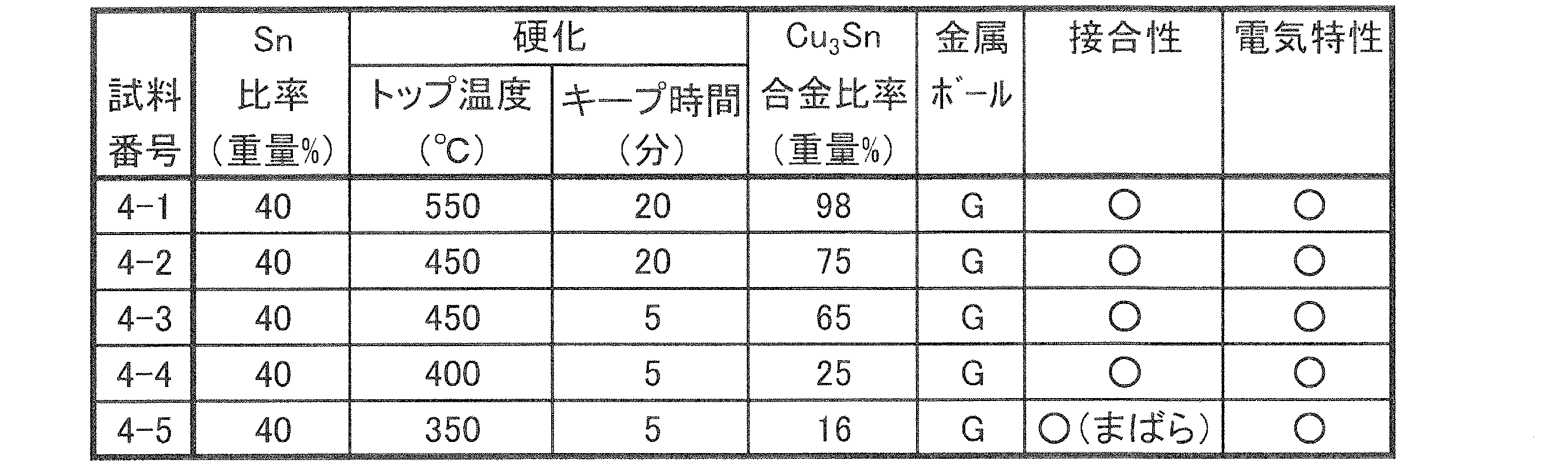
硬化時のトップ温度を低くすると、配合したCu粉とSn粉との相互拡散が促進されにくいため、導通層に含まれるSnおよびCuの合計量に対するCu3Sn合金比率が低くなった。
(1)熱硬化型導電性樹脂組成物の作製
Sn粉末およびCu粉末の合計量に対するSn粉末の比率を40重量%に固定し、代わりに、熱硬化性樹脂として、表3の「熱硬化性樹脂の種類」の欄に示したものを用いたことを除いて、実験例1と同様の操作を経て、試料となる未硬化の熱硬化型導電性樹脂組成物を得た。
実験例1と同様の条件を適用しながら、積層セラミックコンデンサのための部品本体としての積層体の両端面に熱硬化型導電性樹脂組成物を付与し、熱処理することによって、外部電極における導通層が両端面に形成された積層体を得た。
実験例1と同様の条件を適用しながら、導通層上に、Niめっき層およびSnめっき層を形成し、試料となる積層セラミックコンデンサを得た。
表3に示すように、実験例1において評価した「硬化後残留応力」、「金属ボール」「接合性」、および「電気特性」を評価した。

実験例1における試料4では、熱硬化性樹脂として、レゾール型フェノール樹脂Aを用い、表1に示すように、「硬化後残留応力」は10MPaであった。実験例3においては、表3に示すように、試料11では、「熱硬化性樹脂の種類」がレゾール型フェノール樹脂Bであり、「硬化後残留応力」は8MPaであった。これら試料4および11では、「金属ボール」「接合性」、および「電気特性」のすべてにおいて、良好な結果が得られた。
(1)熱硬化型導電性樹脂組成物の作製
Sn粉末およびCu粉末の合計量に対するSn粉末の比率を40重量%に固定し、代わりに、熱硬化型導電性樹脂組成物中での有機溶剤を除いてのCu粉末とSn粉末との合計含有量、すなわち、「乾燥後の金属含有率」を表4に示すように変えたことを除いて、実験例1と同様の操作を経て、試料となる未硬化の熱硬化型導電性樹脂組成物を得た。
実験例1と同様の条件を適用しながら、積層セラミックコンデンサのための部品本体としての積層体の両端面に熱硬化型導電性樹脂組成物を付与し、熱処理することによって、外部電極における導通層が両端面に形成された積層体を得た。
実験例1と同様の条件を適用しながら、導通層上に、Niめっき層およびSnめっき層を形成し、試料となる積層セラミックコンデンサを得た。
表4に示すように、実験例1において評価した「金属ボール」「接合性」、および「電気特性」を評価した。
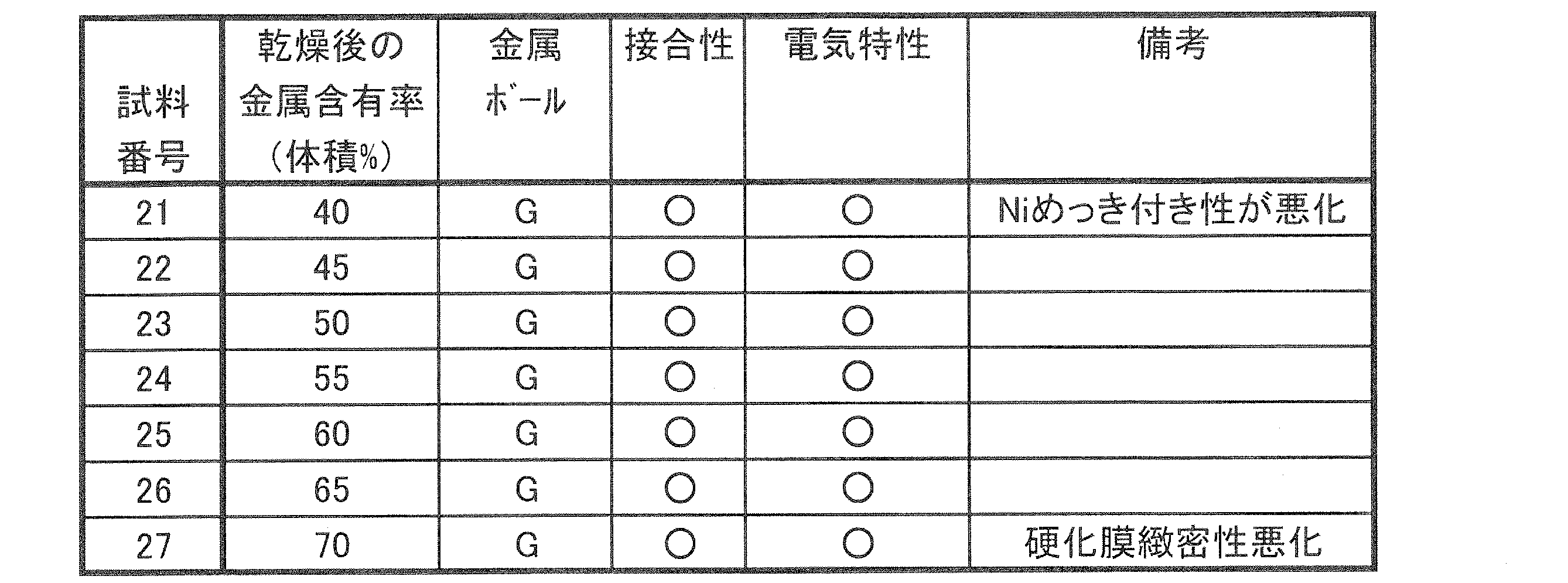
表4に示すように、「乾燥後の金属含有率」が、それぞれ、40体積%、45体積%、50体積%、55体積%、60体積%、65体積%および70体積%である試料21、試料22、試料23、試料24、試料25、試料26および試料27では、「金属ボール」「接合性」、および「電気特性」のすべてにおいて、良好な結果が得られた。
(1)熱硬化型導電性樹脂組成物の作製
Sn粉末およびCu粉末の合計量に対するSn粉末の比率を40重量%に固定し、代わりに、「Cu粉末のD50」を表5に示すように変えたことを除いて、実験例1と同様の操作を経て、試料となる未硬化の熱硬化型導電性樹脂組成物を得た。
実験例1と同様の条件を適用しながら、積層セラミックコンデンサのための部品本体としての積層体の両端面に熱硬化型導電性樹脂組成物を付与し、熱処理することによって、外部電極における導通層が両端面に形成された積層体を得た。
実験例1と同様の条件を適用しながら、導通層上に、Niめっき層およびSnめっき層を形成し、試料となる積層セラミックコンデンサを得た。
表5に示すように、実験例1において評価した「金属ボール」「接合性」、および「電気特性」を評価した。
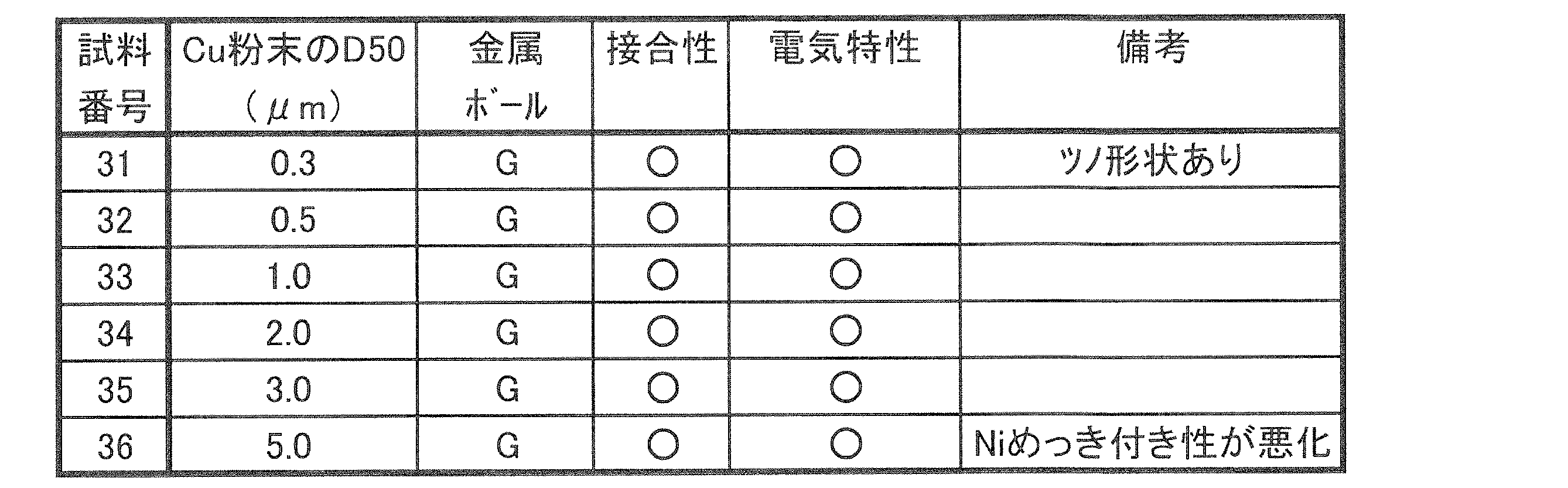
表5に示すように、「Cu粉末のD50」が、それぞれ、0.3μm、0.5μm、1.0μm、2.0μm、3.0μmおよび5.0μmである試料31、試料32、試料33、試料34、試料35および試料36では、「金属ボール」「接合性」、および「電気特性」のすべてにおいて、良好な結果が得られた。
(1)熱硬化型導電性樹脂組成物の作製
Sn粉末およびCu粉末の合計量に対するSn粉末の比率を40重量%に固定し、代わりに、「Sn粉末のD50」を表6に示すように変えたことを除いて、実験例1と同様の操作を経て、試料となる未硬化の熱硬化型導電性樹脂組成物を得た。
実験例1と同様の条件を適用しながら、積層セラミックコンデンサのための部品本体としての積層体の両端面に熱硬化型導電性樹脂組成物を付与し、熱処理することによって、外部電極における導通層が両端面に形成された積層体を得た。
実験例1と同様の条件を適用しながら、導通層上に、Niめっき層およびSnめっき層を形成し、試料となる積層セラミックコンデンサを得た。
表6に示すように、実験例1において評価した「金属ボール」「接合性」、および「電気特性」を評価した。
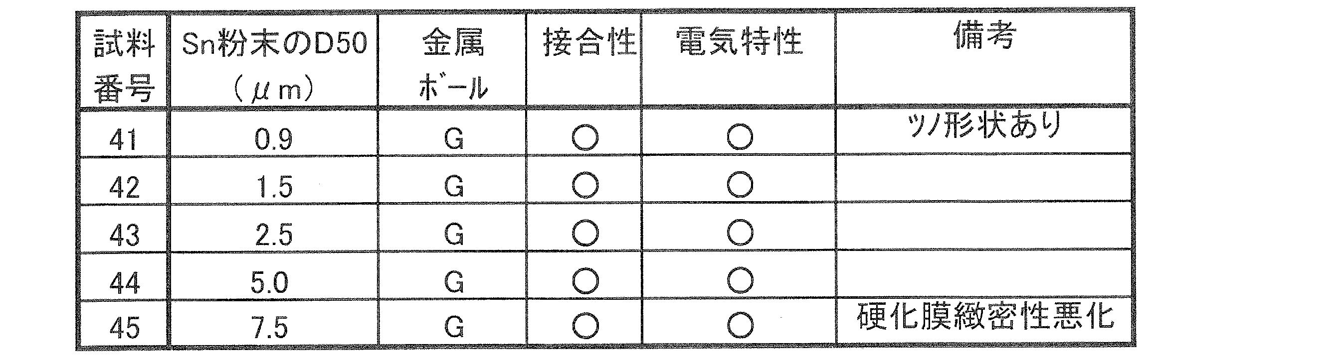
表6に示すように、「Sn粉末のD50」が、それぞれ、0.9μm、1.5μm、2.5μm、5.0μmおよび7.5μmである試料41、試料42、試料43、試料44および試料45では、「金属ボール」「接合性」、および「電気特性」のすべてにおいて、良好な結果が得られた。
(1)熱硬化型導電性樹脂組成物の作製
Sn粉末およびCu粉末の合計量に対するSn粉末の比率を40重量%に固定し、代わりに、表7に示すように、試料51では、「Cu粉末の形状」を扁平としたことを除いて、実験例1と同様の操作を経て、試料となる未硬化の熱硬化型導電性樹脂組成物を得た。
基本的には、実験例1と同様の条件を適用しながら、積層セラミックコンデンサのための部品本体としての積層体の両端面に熱硬化型導電性樹脂組成物を付与し、熱処理することによって、外部電極における導通層が両端面に形成された積層体を得た。異なる点は以下のとおりである。
実験例1と同様の条件を適用しながら、導通層上に、Niめっき層およびSnめっき層を形成し、試料となる積層セラミックコンデンサを得た。
表7に示すように、実験例1において評価した「金属ボール」「接合性」、および「電気特性」を評価した。

表7に示すように、試料51~53のいずれにおいても、「金属ボール」「接合性」、および「電気特性」のすべてについて、良好な結果が得られた。
(1)熱硬化型導電性樹脂組成物の作製
Sn粉末およびCu粉末の合計量に対するSn粉末の比率を、特許文献2の請求項3に記載の比率に従い、表8の「Sn比率」の欄に示すように変えたことを除いて、実験例1と同様の操作を経て、試料となる未硬化の熱硬化型導電性樹脂組成物を得た。
表8の「硬化トップ温度」の欄に示すように、試料62および64については、熱硬化型導電性樹脂組成物の硬化のための熱処理トップ温度を550℃としたことを除いて、実験例1と同様の条件を適用しながら、積層セラミックコンデンサのための部品本体としての積層体の両端面に熱硬化型導電性樹脂組成物を付与し、熱処理することによって、外部電極における導通層が両端面に形成された積層体を得た。
実験例1と同様の条件を適用しながら、導通層上に、Niめっき層およびSnめっき層を形成し、試料となる積層セラミックコンデンサを得た。
表8に示すように、実験例1において評価した「硬化後残留応力」、「金属ボール」「接合性」、および「電気特性」を評価した。

表8に示すように、試料61~64では、8MPa以上の「硬化後残留応力」が得られ、「金属ボール」についても「G」の評価が得られた。
(1)熱硬化型導電性樹脂組成物の作製
Cu粉末に代えてAg粉末を用い、かつAg粉末およびSn粉末の合計量に対するSn粉末の比率を、特許文献2の請求項3に規定された低融点側の金属の比率の上限である20重量%に固定したことを除いて、実験例1と同様の操作を経て、試料となる未硬化の熱硬化型導電性樹脂組成物を得た。
表9の「硬化トップ温度」の欄に示すように、熱硬化型導電性樹脂組成物の硬化のための熱処理トップ温度を適用しながら、その他の条件については、実験例1と同様の条件で、積層セラミックコンデンサのための部品本体としての積層体の両端面に熱硬化型導電性樹脂組成物を付与し、熱処理することによって、外部電極における導通層が両端面に形成された積層体を得た。
実験例1と同様の条件を適用しながら、導通層上に、Niめっき層およびSnめっき層を形成し、試料となる積層セラミックコンデンサを得た。
表9に示すように、実験例1において評価した「硬化後残留応力」、「金属ボール」「接合性」、および「電気特性」を評価した。

表9に示すように、試料71および72では、8MPa以上の「硬化後残留応力」が得られた。
2 セラミック層
3,4 内部電極
5 積層体
8,9 外部電極
10 導通層
11 Niめっき層
12 Snめっき層
21 熱硬化型導電性樹脂組成物
22 Cu粉末
23 Sn粉末
24 熱硬化性樹脂
25 金属粒子
Claims (2)
- セラミック層と内部電極とが積層された積層体と、
前記内部電極と電気的に接続されるように、前記積層体の外表面上に形成された外部電極と
を備え、
前記外部電極は、前記内部電極に接する導通層を含み、
前記導通層は、Cu3Sn合金を含む金属粒子と熱硬化性樹脂とを含み、
前記内部電極はNiを含み、
前記内部電極と前記導通層とは、CuSnNi合金相を介して接合されている、
積層セラミック電子部品。 - 前記CuSnNi合金相中のNi固溶量は5~42atm%である、請求項1に記載の積層セラミック電子部品。
Priority Applications (4)
| Application Number | Priority Date | Filing Date | Title |
|---|---|---|---|
| CN201380063394.9A CN104823252B (zh) | 2012-12-18 | 2013-11-23 | 层叠陶瓷电子部件 |
| KR1020157016120A KR101775913B1 (ko) | 2012-12-18 | 2013-11-23 | 적층 세라믹 전자부품 |
| JP2014553040A JP6094597B2 (ja) | 2012-12-18 | 2013-11-23 | 積層セラミック電子部品 |
| US14/739,301 US9627133B2 (en) | 2012-12-18 | 2015-06-15 | Laminated ceramic electronic component |
Applications Claiming Priority (2)
| Application Number | Priority Date | Filing Date | Title |
|---|---|---|---|
| JP2012-275526 | 2012-12-18 | ||
| JP2012275526 | 2012-12-18 |
Related Child Applications (1)
| Application Number | Title | Priority Date | Filing Date |
|---|---|---|---|
| US14/739,301 Continuation US9627133B2 (en) | 2012-12-18 | 2015-06-15 | Laminated ceramic electronic component |
Publications (1)
| Publication Number | Publication Date |
|---|---|
| WO2014097823A1 true WO2014097823A1 (ja) | 2014-06-26 |
Family
ID=50978164
Family Applications (2)
| Application Number | Title | Priority Date | Filing Date |
|---|---|---|---|
| PCT/JP2013/081569 Ceased WO2014097823A1 (ja) | 2012-12-18 | 2013-11-23 | 積層セラミック電子部品 |
| PCT/JP2013/081568 Ceased WO2014097822A1 (ja) | 2012-12-18 | 2013-11-23 | 積層セラミック電子部品 |
Family Applications After (1)
| Application Number | Title | Priority Date | Filing Date |
|---|---|---|---|
| PCT/JP2013/081568 Ceased WO2014097822A1 (ja) | 2012-12-18 | 2013-11-23 | 積層セラミック電子部品 |
Country Status (6)
| Country | Link |
|---|---|
| US (2) | US9881737B2 (ja) |
| JP (2) | JP6094597B2 (ja) |
| KR (2) | KR101775914B1 (ja) |
| CN (2) | CN104823252B (ja) |
| TW (2) | TWI536412B (ja) |
| WO (2) | WO2014097823A1 (ja) |
Cited By (8)
| Publication number | Priority date | Publication date | Assignee | Title |
|---|---|---|---|---|
| JP2017011145A (ja) * | 2015-06-24 | 2017-01-12 | 株式会社村田製作所 | 積層セラミックコンデンサ |
| US20170032896A1 (en) * | 2015-07-30 | 2017-02-02 | Murata Manufacturing Co., Ltd. | Multilayer ceramic capacitor and manufacturing method therefor |
| JP2017191929A (ja) * | 2016-04-15 | 2017-10-19 | サムソン エレクトロ−メカニックス カンパニーリミテッド. | 積層型キャパシター及びその製造方法 |
| JP2018098475A (ja) * | 2016-12-09 | 2018-06-21 | 株式会社村田製作所 | 積層セラミックコンデンサ |
| JP2019220602A (ja) * | 2018-06-21 | 2019-12-26 | 株式会社村田製作所 | 電子部品および電子部品の製造方法 |
| JP2020088372A (ja) * | 2018-11-29 | 2020-06-04 | サムソン エレクトロ−メカニックス カンパニーリミテッド. | 積層セラミックキャパシタ |
| JP2020126896A (ja) * | 2019-02-01 | 2020-08-20 | Tdk株式会社 | セラミック電子部品 |
| JP2022067608A (ja) * | 2020-10-20 | 2022-05-06 | サムソン エレクトロ-メカニックス カンパニーリミテッド. | 積層型電子部品 |
Families Citing this family (36)
| Publication number | Priority date | Publication date | Assignee | Title |
|---|---|---|---|---|
| CN104823252B (zh) * | 2012-12-18 | 2018-04-06 | 株式会社村田制作所 | 层叠陶瓷电子部件 |
| JP6112060B2 (ja) * | 2013-06-19 | 2017-04-12 | 株式会社村田製作所 | セラミック電子部品およびその製造方法 |
| JP2015026816A (ja) * | 2013-06-19 | 2015-02-05 | 株式会社村田製作所 | セラミック電子部品およびその製造方法 |
| KR102097329B1 (ko) * | 2013-09-12 | 2020-04-06 | 삼성전기주식회사 | 적층 세라믹 커패시터, 그 제조방법 및 적층 세라믹 커패시터 실장 기판 |
| JP6378122B2 (ja) * | 2014-12-05 | 2018-08-22 | 太陽誘電株式会社 | 積層セラミック電子部品 |
| KR102139753B1 (ko) * | 2015-02-26 | 2020-07-31 | 삼성전기주식회사 | 세라믹 전자 부품 및 이의 제조방법 |
| JP6597008B2 (ja) * | 2015-07-16 | 2019-10-30 | 株式会社村田製作所 | 積層セラミックコンデンサ及び積層セラミックコンデンサの製造方法 |
| US10236123B2 (en) * | 2015-07-19 | 2019-03-19 | Vq Research, Inc. | Methods and systems to minimize delamination of multilayer ceramic capacitors |
| KR101973433B1 (ko) | 2016-04-15 | 2019-04-29 | 삼성전기주식회사 | 적층형 커패시터 및 그 제조 방법 |
| KR101892802B1 (ko) | 2016-04-25 | 2018-08-28 | 삼성전기주식회사 | 적층형 커패시터 및 그 실장 기판 |
| US10580567B2 (en) * | 2016-07-26 | 2020-03-03 | Samsung Electro-Mechanics Co., Ltd. | Coil component and method of manufacturing the same |
| KR101892819B1 (ko) | 2016-07-26 | 2018-08-28 | 삼성전기주식회사 | 코일 부품 |
| KR102105345B1 (ko) * | 2016-12-09 | 2020-04-28 | 가부시키가이샤 무라타 세이사쿠쇼 | 적층 세라믹 콘덴서 |
| KR101941954B1 (ko) | 2017-07-04 | 2019-01-24 | 삼성전기 주식회사 | 적층 세라믹 커패시터 |
| US10770230B2 (en) | 2017-07-04 | 2020-09-08 | Samsung Electro-Mechanics Co., Ltd. | Multilayer ceramic capacitor and method of manufacturing the same |
| KR101973441B1 (ko) | 2017-07-04 | 2019-09-02 | 삼성전기주식회사 | 적층 세라믹 커패시터 및 그 제조방법 |
| JP6919515B2 (ja) * | 2017-11-15 | 2021-08-18 | 株式会社村田製作所 | 積層セラミックコンデンサ |
| JP7089404B2 (ja) * | 2018-05-22 | 2022-06-22 | 太陽誘電株式会社 | セラミック電子部品およびその製造方法 |
| KR102789045B1 (ko) * | 2018-10-17 | 2025-04-01 | 삼성전기주식회사 | 적층 세라믹 전자부품 및 그 제조방법 |
| KR102734416B1 (ko) | 2018-11-29 | 2024-11-27 | 삼성전기주식회사 | 적층 세라믹 커패시터 |
| KR102772046B1 (ko) | 2019-09-20 | 2025-02-25 | 삼성전기주식회사 | 적층 세라믹 전자부품 |
| JP7668086B2 (ja) * | 2019-09-30 | 2025-04-24 | 太陽誘電株式会社 | コイル部品、回路基板及び電子機器 |
| KR102281451B1 (ko) * | 2019-10-16 | 2021-07-27 | 삼성전기주식회사 | 전고체 전지 |
| KR20220166340A (ko) * | 2020-05-19 | 2022-12-16 | 교세라 가부시키가이샤 | 콘덴서 |
| KR102813236B1 (ko) * | 2020-06-02 | 2025-05-27 | 삼성전기주식회사 | 전자 부품 및 그 제조방법 |
| WO2022065004A1 (ja) * | 2020-09-25 | 2022-03-31 | 株式会社村田製作所 | チップ型セラミック電子部品およびその製造方法 |
| KR102867013B1 (ko) | 2020-11-23 | 2025-10-01 | 삼성전기주식회사 | 적층형 전자 부품 |
| KR102533750B1 (ko) * | 2021-06-22 | 2023-05-18 | 삼화콘덴서공업 주식회사 | 적층 세라믹 커패시터의 외부전극용 도전성 페이스트 조성물 |
| KR102505434B1 (ko) * | 2021-10-19 | 2023-03-03 | 삼성전기주식회사 | 적층형 전자 부품 |
| KR102933568B1 (ko) | 2021-11-03 | 2026-03-04 | 삼성전기주식회사 | 적층형 커패시터 |
| KR102881004B1 (ko) | 2021-11-11 | 2025-11-04 | 삼성전기주식회사 | 복합 전자부품 |
| KR102881362B1 (ko) * | 2021-12-20 | 2025-11-04 | 삼성전기주식회사 | 적층형 전자부품 |
| KR20230172183A (ko) * | 2022-06-15 | 2023-12-22 | 삼성전기주식회사 | 적층형 전자 부품 |
| KR102937458B1 (ko) * | 2022-11-24 | 2026-03-12 | 한국과학기술연구원 | 프러시안 블루 기반 응집제 및 이를 이용한 미세플라스틱 응집방법 |
| KR20240092958A (ko) * | 2022-12-15 | 2024-06-24 | 삼성전기주식회사 | 적층형 전자 부품 |
| KR102873140B1 (ko) * | 2023-01-30 | 2025-10-20 | 가부시키가이샤 무라타 세이사쿠쇼 | 적층 세라믹 전자부품, 페이스트, 및 적층 세라믹 전자부품의 제조 방법 |
Citations (3)
| Publication number | Priority date | Publication date | Assignee | Title |
|---|---|---|---|---|
| JPH11307930A (ja) * | 1998-04-24 | 1999-11-05 | Namics Corp | 基板およびその製造方法 |
| WO2004053901A1 (ja) * | 2002-12-09 | 2004-06-24 | Matsushita Electric Industrial Co., Ltd. | 外部電極を備えた電子部品 |
| WO2007072894A1 (ja) * | 2005-12-22 | 2007-06-28 | Namics Corporation | 熱硬化性導電ペースト及びそれを用いて形成した外部電極を有する積層セラミック部品 |
Family Cites Families (17)
| Publication number | Priority date | Publication date | Assignee | Title |
|---|---|---|---|---|
| JP2658509B2 (ja) * | 1989-06-16 | 1997-09-30 | 松下電器産業株式会社 | 電子部品と電極ペーストおよび端子電極の形成方法 |
| JP2895793B2 (ja) * | 1995-02-24 | 1999-05-24 | マブチモーター株式会社 | 摺動接点材料及びクラッド複合材ならびにそれらからなるコンミテータ及びそのコンミテータを使用した直流小型モータ |
| JPH10279903A (ja) | 1997-04-04 | 1998-10-20 | Asahi Chem Ind Co Ltd | 導電性接着剤 |
| JP2001118424A (ja) * | 1999-10-19 | 2001-04-27 | Kawatetsu Mining Co Ltd | 導電ペースト用銅合金粉 |
| JP3472523B2 (ja) * | 2000-02-29 | 2003-12-02 | 京セラ株式会社 | 電気素子内蔵配線基板 |
| JP2001244467A (ja) | 2000-02-28 | 2001-09-07 | Hitachi Ltd | コプラナー型半導体装置とそれを用いた表示装置および製法 |
| JP2002198654A (ja) * | 2000-12-25 | 2002-07-12 | Kyocera Corp | 電気素子内蔵配線基板およびその製造方法 |
| CA2359347A1 (en) * | 2001-10-18 | 2003-04-18 | Cesur Celik | Laminated ceramic capacitor internal electrode material |
| WO2006022060A1 (ja) * | 2004-08-27 | 2006-03-02 | Murata Manufacturing Co., Ltd. | 積層セラミックコンデンサおよびその等価直列抵抗調整方法 |
| JP2007035848A (ja) * | 2005-07-26 | 2007-02-08 | Taiyo Yuden Co Ltd | 積層セラミックコンデンサ及びその製造方法 |
| JP4934456B2 (ja) * | 2006-02-20 | 2012-05-16 | 古河電気工業株式会社 | めっき材料および前記めっき材料が用いられた電気電子部品 |
| EP2058822A4 (en) * | 2006-08-28 | 2011-01-05 | Murata Manufacturing Co | CONDUCTIVE BINDER AND ELECTRONIC DEVICE |
| JP2009141292A (ja) * | 2007-12-11 | 2009-06-25 | Taiyo Kagaku Kogyo Kk | 外部端子電極具備電子部品、その搭載電子用品及び外部端子電極具備電子部品の製造方法 |
| JP5115349B2 (ja) * | 2008-06-13 | 2013-01-09 | 株式会社村田製作所 | 積層セラミック電子部品およびその製造方法 |
| JPWO2012128175A1 (ja) * | 2011-03-18 | 2014-07-24 | 株式会社村田製作所 | 積層セラミックコンデンサ、誘電体セラミック、積層セラミック電子部品および積層セラミックコンデンサの製造方法 |
| CN102222564B (zh) * | 2011-03-31 | 2012-11-28 | 亿曼丰科技(深圳)有限公司 | 基于平衡电极内浆和陶瓷膜收缩率的mlcc电容器 |
| CN104823252B (zh) * | 2012-12-18 | 2018-04-06 | 株式会社村田制作所 | 层叠陶瓷电子部件 |
-
2013
- 2013-11-23 CN CN201380063394.9A patent/CN104823252B/zh active Active
- 2013-11-23 CN CN201380066173.7A patent/CN104871271B/zh active Active
- 2013-11-23 KR KR1020157016121A patent/KR101775914B1/ko active Active
- 2013-11-23 WO PCT/JP2013/081569 patent/WO2014097823A1/ja not_active Ceased
- 2013-11-23 JP JP2014553040A patent/JP6094597B2/ja active Active
- 2013-11-23 KR KR1020157016120A patent/KR101775913B1/ko active Active
- 2013-11-23 JP JP2014553039A patent/JP6094596B2/ja active Active
- 2013-11-23 WO PCT/JP2013/081568 patent/WO2014097822A1/ja not_active Ceased
- 2013-12-13 TW TW102146264A patent/TWI536412B/zh active
- 2013-12-13 TW TW102146263A patent/TWI585794B/zh active
-
2015
- 2015-06-11 US US14/736,739 patent/US9881737B2/en active Active
- 2015-06-15 US US14/739,301 patent/US9627133B2/en active Active
Patent Citations (3)
| Publication number | Priority date | Publication date | Assignee | Title |
|---|---|---|---|---|
| JPH11307930A (ja) * | 1998-04-24 | 1999-11-05 | Namics Corp | 基板およびその製造方法 |
| WO2004053901A1 (ja) * | 2002-12-09 | 2004-06-24 | Matsushita Electric Industrial Co., Ltd. | 外部電極を備えた電子部品 |
| WO2007072894A1 (ja) * | 2005-12-22 | 2007-06-28 | Namics Corporation | 熱硬化性導電ペースト及びそれを用いて形成した外部電極を有する積層セラミック部品 |
Cited By (22)
| Publication number | Priority date | Publication date | Assignee | Title |
|---|---|---|---|---|
| JP2017011145A (ja) * | 2015-06-24 | 2017-01-12 | 株式会社村田製作所 | 積層セラミックコンデンサ |
| US20170032896A1 (en) * | 2015-07-30 | 2017-02-02 | Murata Manufacturing Co., Ltd. | Multilayer ceramic capacitor and manufacturing method therefor |
| US10269494B2 (en) * | 2015-07-30 | 2019-04-23 | Murata Manufacturing Co., Ltd. | Multilayer ceramic capacitor including external electrodes with multilayer structure and manufacturing method therefor |
| JP7048163B2 (ja) | 2016-04-15 | 2022-04-05 | サムソン エレクトロ-メカニックス カンパニーリミテッド. | 積層型キャパシター及びその製造方法 |
| JP2017191929A (ja) * | 2016-04-15 | 2017-10-19 | サムソン エレクトロ−メカニックス カンパニーリミテッド. | 積層型キャパシター及びその製造方法 |
| JP2019125794A (ja) * | 2016-04-15 | 2019-07-25 | サムソン エレクトロ−メカニックス カンパニーリミテッド. | 積層型キャパシター及びその製造方法 |
| US10446320B2 (en) | 2016-04-15 | 2019-10-15 | Samsung Electro-Mechanics Co., Ltd. | Multilayer capacitor having external electrode including conductive resin layer |
| US10658116B2 (en) | 2016-04-15 | 2020-05-19 | Samsung Electro-Mechanics Co., Ltd. | Multilayer capacitor having external electrode including conductive resin layer |
| US10658117B2 (en) | 2016-04-15 | 2020-05-19 | Samsung Electro-Mechanics Co., Ltd. | Multilayer capacitor having external electrode including conductive resin layer |
| US11342119B2 (en) | 2016-04-15 | 2022-05-24 | Samsung Electro-Mechanics Co., Ltd. | Multilayer capacitor having external electrode including conductive resin layer |
| JP2018098475A (ja) * | 2016-12-09 | 2018-06-21 | 株式会社村田製作所 | 積層セラミックコンデンサ |
| JP2019220602A (ja) * | 2018-06-21 | 2019-12-26 | 株式会社村田製作所 | 電子部品および電子部品の製造方法 |
| JP2020088372A (ja) * | 2018-11-29 | 2020-06-04 | サムソン エレクトロ−メカニックス カンパニーリミテッド. | 積層セラミックキャパシタ |
| JP2022031927A (ja) * | 2018-11-29 | 2022-02-22 | サムソン エレクトロ-メカニックス カンパニーリミテッド. | 積層セラミックキャパシタ |
| US10903010B2 (en) | 2018-11-29 | 2021-01-26 | Samsung Electro-Mechanics Co., Ltd. | Multilayer ceramic capacitor |
| JP7053095B2 (ja) | 2018-11-29 | 2022-04-12 | サムソン エレクトロ-メカニックス カンパニーリミテッド. | 積層セラミックキャパシタ |
| US11393628B2 (en) | 2018-11-29 | 2022-07-19 | Samsung Electro-Mechanics Co., Ltd. | Multilayer ceramic capacitor |
| JP7302900B2 (ja) | 2018-11-29 | 2023-07-04 | サムソン エレクトロ-メカニックス カンパニーリミテッド. | 積層セラミックキャパシタ |
| JP2020126896A (ja) * | 2019-02-01 | 2020-08-20 | Tdk株式会社 | セラミック電子部品 |
| JP7276646B2 (ja) | 2019-02-01 | 2023-05-18 | Tdk株式会社 | セラミック電子部品 |
| JP2022067608A (ja) * | 2020-10-20 | 2022-05-06 | サムソン エレクトロ-メカニックス カンパニーリミテッド. | 積層型電子部品 |
| JP7732136B2 (ja) | 2020-10-20 | 2025-09-02 | サムソン エレクトロ-メカニックス カンパニーリミテッド. | 積層型電子部品 |
Also Published As
| Publication number | Publication date |
|---|---|
| TWI585794B (zh) | 2017-06-01 |
| TW201435941A (zh) | 2014-09-16 |
| CN104871271A (zh) | 2015-08-26 |
| US9881737B2 (en) | 2018-01-30 |
| WO2014097822A1 (ja) | 2014-06-26 |
| TW201440100A (zh) | 2014-10-16 |
| CN104823252B (zh) | 2018-04-06 |
| US20150279566A1 (en) | 2015-10-01 |
| US20150279563A1 (en) | 2015-10-01 |
| US9627133B2 (en) | 2017-04-18 |
| KR20150086342A (ko) | 2015-07-27 |
| JPWO2014097822A1 (ja) | 2017-01-12 |
| CN104871271B (zh) | 2018-04-20 |
| KR101775913B1 (ko) | 2017-09-07 |
| KR101775914B1 (ko) | 2017-09-07 |
| JPWO2014097823A1 (ja) | 2017-01-12 |
| CN104823252A (zh) | 2015-08-05 |
| JP6094597B2 (ja) | 2017-03-15 |
| TWI536412B (zh) | 2016-06-01 |
| JP6094596B2 (ja) | 2017-03-15 |
| KR20150086343A (ko) | 2015-07-27 |
Similar Documents
| Publication | Publication Date | Title |
|---|---|---|
| JP6094597B2 (ja) | 積層セラミック電子部品 | |
| JP5246207B2 (ja) | チップ型電子部品 | |
| KR102952186B1 (ko) | 도전성 수지 조성물 | |
| JP6623574B2 (ja) | 積層セラミックコンデンサ | |
| JP2017034010A (ja) | 積層セラミックコンデンサおよびその製造方法 | |
| JP6852846B2 (ja) | 電極用ペーストおよび積層セラミック電子部品 | |
| JP7078195B2 (ja) | 電子部品の製造方法 | |
| JP2014003048A (ja) | 電子部品の製造方法 |
Legal Events
| Date | Code | Title | Description |
|---|---|---|---|
| 121 | Ep: the epo has been informed by wipo that ep was designated in this application |
Ref document number: 13864547 Country of ref document: EP Kind code of ref document: A1 |
|
| ENP | Entry into the national phase |
Ref document number: 2014553040 Country of ref document: JP Kind code of ref document: A |
|
| ENP | Entry into the national phase |
Ref document number: 20157016120 Country of ref document: KR Kind code of ref document: A |
|
| NENP | Non-entry into the national phase |
Ref country code: DE |
|
| 122 | Ep: pct application non-entry in european phase |
Ref document number: 13864547 Country of ref document: EP Kind code of ref document: A1 |