WO2012002304A1 - 2次電池用負極、負極集電体及びこれらの製造方法、並びに2次電池 - Google Patents
2次電池用負極、負極集電体及びこれらの製造方法、並びに2次電池 Download PDFInfo
- Publication number
- WO2012002304A1 WO2012002304A1 PCT/JP2011/064632 JP2011064632W WO2012002304A1 WO 2012002304 A1 WO2012002304 A1 WO 2012002304A1 JP 2011064632 W JP2011064632 W JP 2011064632W WO 2012002304 A1 WO2012002304 A1 WO 2012002304A1
- Authority
- WO
- WIPO (PCT)
- Prior art keywords
- negative electrode
- active material
- current collector
- secondary battery
- silicon
- Prior art date
- Legal status (The legal status is an assumption and is not a legal conclusion. Google has not performed a legal analysis and makes no representation as to the accuracy of the status listed.)
- Ceased
Links
Images


Classifications
-
- H—ELECTRICITY
- H01—ELECTRIC ELEMENTS
- H01M—PROCESSES OR MEANS, e.g. BATTERIES, FOR THE DIRECT CONVERSION OF CHEMICAL ENERGY INTO ELECTRICAL ENERGY
- H01M4/00—Electrodes
- H01M4/02—Electrodes composed of, or comprising, active material
- H01M4/64—Carriers or collectors
- H01M4/66—Selection of materials
- H01M4/661—Metal or alloys, e.g. alloy coatings
-
- H—ELECTRICITY
- H01—ELECTRIC ELEMENTS
- H01M—PROCESSES OR MEANS, e.g. BATTERIES, FOR THE DIRECT CONVERSION OF CHEMICAL ENERGY INTO ELECTRICAL ENERGY
- H01M10/00—Secondary cells; Manufacture thereof
- H01M10/05—Accumulators with non-aqueous electrolyte
- H01M10/052—Li-accumulators
-
- H—ELECTRICITY
- H01—ELECTRIC ELEMENTS
- H01M—PROCESSES OR MEANS, e.g. BATTERIES, FOR THE DIRECT CONVERSION OF CHEMICAL ENERGY INTO ELECTRICAL ENERGY
- H01M4/00—Electrodes
- H01M4/02—Electrodes composed of, or comprising, active material
- H01M4/04—Processes of manufacture in general
- H01M4/0402—Methods of deposition of the material
- H01M4/0404—Methods of deposition of the material by coating on electrode collectors
-
- H—ELECTRICITY
- H01—ELECTRIC ELEMENTS
- H01M—PROCESSES OR MEANS, e.g. BATTERIES, FOR THE DIRECT CONVERSION OF CHEMICAL ENERGY INTO ELECTRICAL ENERGY
- H01M4/00—Electrodes
- H01M4/02—Electrodes composed of, or comprising, active material
- H01M4/13—Electrodes for accumulators with non-aqueous electrolyte, e.g. for lithium-accumulators; Processes of manufacture thereof
- H01M4/134—Electrodes based on metals, Si or alloys
-
- H—ELECTRICITY
- H01—ELECTRIC ELEMENTS
- H01M—PROCESSES OR MEANS, e.g. BATTERIES, FOR THE DIRECT CONVERSION OF CHEMICAL ENERGY INTO ELECTRICAL ENERGY
- H01M4/00—Electrodes
- H01M4/02—Electrodes composed of, or comprising, active material
- H01M4/13—Electrodes for accumulators with non-aqueous electrolyte, e.g. for lithium-accumulators; Processes of manufacture thereof
- H01M4/139—Processes of manufacture
- H01M4/1395—Processes of manufacture of electrodes based on metals, Si or alloys
-
- H—ELECTRICITY
- H01—ELECTRIC ELEMENTS
- H01M—PROCESSES OR MEANS, e.g. BATTERIES, FOR THE DIRECT CONVERSION OF CHEMICAL ENERGY INTO ELECTRICAL ENERGY
- H01M4/00—Electrodes
- H01M4/02—Electrodes composed of, or comprising, active material
- H01M4/36—Selection of substances as active materials, active masses, active liquids
- H01M4/362—Composites
- H01M4/364—Composites as mixtures
-
- H—ELECTRICITY
- H01—ELECTRIC ELEMENTS
- H01M—PROCESSES OR MEANS, e.g. BATTERIES, FOR THE DIRECT CONVERSION OF CHEMICAL ENERGY INTO ELECTRICAL ENERGY
- H01M4/00—Electrodes
- H01M4/02—Electrodes composed of, or comprising, active material
- H01M4/64—Carriers or collectors
- H01M4/70—Carriers or collectors characterised by shape or form
-
- Y—GENERAL TAGGING OF NEW TECHNOLOGICAL DEVELOPMENTS; GENERAL TAGGING OF CROSS-SECTIONAL TECHNOLOGIES SPANNING OVER SEVERAL SECTIONS OF THE IPC; TECHNICAL SUBJECTS COVERED BY FORMER USPC CROSS-REFERENCE ART COLLECTIONS [XRACs] AND DIGESTS
- Y02—TECHNOLOGIES OR APPLICATIONS FOR MITIGATION OR ADAPTATION AGAINST CLIMATE CHANGE
- Y02E—REDUCTION OF GREENHOUSE GAS [GHG] EMISSIONS, RELATED TO ENERGY GENERATION, TRANSMISSION OR DISTRIBUTION
- Y02E60/00—Enabling technologies; Technologies with a potential or indirect contribution to GHG emissions mitigation
- Y02E60/10—Energy storage using batteries
-
- Y—GENERAL TAGGING OF NEW TECHNOLOGICAL DEVELOPMENTS; GENERAL TAGGING OF CROSS-SECTIONAL TECHNOLOGIES SPANNING OVER SEVERAL SECTIONS OF THE IPC; TECHNICAL SUBJECTS COVERED BY FORMER USPC CROSS-REFERENCE ART COLLECTIONS [XRACs] AND DIGESTS
- Y02—TECHNOLOGIES OR APPLICATIONS FOR MITIGATION OR ADAPTATION AGAINST CLIMATE CHANGE
- Y02P—CLIMATE CHANGE MITIGATION TECHNOLOGIES IN THE PRODUCTION OR PROCESSING OF GOODS
- Y02P70/00—Climate change mitigation technologies in the production process for final industrial or consumer products
- Y02P70/50—Manufacturing or production processes characterised by the final manufactured product
-
- Y—GENERAL TAGGING OF NEW TECHNOLOGICAL DEVELOPMENTS; GENERAL TAGGING OF CROSS-SECTIONAL TECHNOLOGIES SPANNING OVER SEVERAL SECTIONS OF THE IPC; TECHNICAL SUBJECTS COVERED BY FORMER USPC CROSS-REFERENCE ART COLLECTIONS [XRACs] AND DIGESTS
- Y02—TECHNOLOGIES OR APPLICATIONS FOR MITIGATION OR ADAPTATION AGAINST CLIMATE CHANGE
- Y02T—CLIMATE CHANGE MITIGATION TECHNOLOGIES RELATED TO TRANSPORTATION
- Y02T10/00—Road transport of goods or passengers
- Y02T10/60—Other road transportation technologies with climate change mitigation effect
- Y02T10/70—Energy storage systems for electromobility, e.g. batteries
Definitions
- the present invention relates to a chargeable / dischargeable secondary battery, in particular, a negative electrode and a negative electrode current collector used in a lithium ion secondary battery using a nonaqueous electrolyte.
- lithium (Li) ion secondary batteries replace the conventional NiCd batteries and Ni hydrogen batteries due to the high energy density obtained from the high voltages of the positive electrode active material and the negative electrode active material used, and the mainstream of secondary batteries. Occupy the position of.
- a lithium ion secondary battery using a combination of a lithium cobaltate (LiCoO 2 ) -based positive electrode active material standardly used in current Li-ion batteries and a carbon-based negative electrode active material mainly composed of graphite is a recent high function.
- the power consumption of high-load electronic components cannot be sufficiently supplied for a long time, and the required specifications cannot be satisfied as a portable power source.
- the theoretical electrochemical specific capacity of the positive electrode active material is generally small, and even if it is a candidate for a new material aiming at practical use in the future, it will be smaller than the theoretical specific capacity of the current carbon-based negative electrode active material.
- the carbon-based negative electrode whose performance has been improved year by year is approaching the limit of the theoretical specific capacity, and the combination of the current positive and negative active material systems is no longer expected to greatly improve the power capacity.
- There are limits to the future demands for higher functionality and longer portability of electronic devices, and mounting in industrial applications such as electric tools, uninterruptible power supplies, power storage devices, and electric vehicles.
- a metal-based negative electrode active material in place of the carbon (C) -based negative electrode active material is being studied as a method capable of dramatically increasing the electric capacity from the current level.
- This is a material using germanium (Ge), tin (Sn), or silicon (Si) -based material having a theoretical specific capacity several times to ten times that of the current C-based negative electrode as the negative electrode active material. Since it has a specific capacity comparable to that of metal Li, which is considered difficult to put into practical use, it is the center of investigation.
- the basic performance required for the secondary battery is that the electric capacity that can be retained by charging is large, and that the electric capacity can be maintained as much as possible even by use cycles in which charging and discharging are repeated.
- JP 2002-319408 A Japanese Patent No. 3935067 Japanese Patent No. 3581784
- An object of the present invention is to provide a negative electrode, a negative electrode current collector, and a secondary battery that can obtain a high capacity by charging and discharging and that can suppress a decrease in capacity as compared with conventional batteries.
- the present inventors were not confined to the conventional knowledge, and as a result of earnestly examining the charge and discharge cycle number and capacity of the negative electrode for Li-ion batteries, and the negative electrode material configuration form, It has been found that the shape of the active material surface formed on the surface of the current collector greatly affects the cycle characteristics.
- the predetermined Si-based negative electrode active material By making the predetermined Si-based negative electrode active material a negative electrode having a predetermined surface shape, the inherent high charge / discharge capacity can be reliably obtained, and the negative electrode can be obtained under good adhesion between the current collector and the active material. It has been found that the charge / discharge cycle life can be maintained long due to the innumerable microsites that can be secured from the surface shape and can be inserted into and desorbed from the active material of Li ions. It is not the most important to define the current collector surface shape, but the surface shape on which the active material is formed is important, and it has been found that a particularly large surface area and an appropriate rough surface shape are desirable. .
- the present invention has been made based on such knowledge.
- long-term cycle life can be regarded as the effect obtained from the roughened shape and unevenness of the electrode surface and the resulting voids in the active material film that provides a long-term cycle life.
- the present inventors have found a relationship between the index representing the roughened surface shape and the negative electrode or negative electrode current collector excellent in charge / discharge characteristics.
- the value is 15 to 50, and the surface roughness (ten-point average roughness) Rz specified by Japanese Industrial Standard (JISB0601-1994 ten-point average roughness) is 1.0 ⁇ m or more and 4.5 ⁇ m or less.
- a negative electrode for a secondary battery (2) The negative electrode for a secondary battery according to (1), wherein the silicon-based active material film contains phosphorus and / or oxygen. (3) The negative electrode for a secondary battery as described in (1), wherein the silicon-based active material film further contains hydrogen. (4) the current in the collector of the silicon-based active material film on the surface formed of, ⁇ 0.003 a layer or zinc to 0.01 ⁇ 0.2 g / m 2 containing nickel 0.05 g / m 2 The negative electrode for a secondary battery according to (1), comprising a heat-resistant layer in which at least one of the layers to be contained is formed.
- a rust preventive layer and / or a silane coupling treatment layer is formed on an upper layer of the heat resistant layer, and further, the silicon-based active material film is formed on the upper layer.
- the negative electrode for secondary batteries as described.
- a current collector for a negative electrode for a secondary battery using a non-aqueous electrolyte which is made of copper foil or copper alloy foil and has a silicon-based active material film formed on one side or both sides, the current collector
- the surface of the surface on which the active material film is formed has a lightness Y value in the XYZ color system (CIE1931 standard color system) of 10 to 40, and the active material film is formed.
- the surface roughness (ten-point average roughness) Rz specified by the Japanese Industrial Standard (JISB0601-1994 ten-point average roughness) is 2.0 ⁇ m or more and 5.0 ⁇ m or less 2 Negative electrode current collector for secondary battery.
- a non-aqueous electrolyte which is made of copper foil or copper alloy foil, and has a silicon-based active material layer formed by solidifying a fine particle active material by slurry coating on one or both sides
- a current collector for a negative electrode wherein the current collector has a tensile strength of 300 MPa or more and 1000 MPa or less, and lightness Y in an XYZ color system (CIE1931 standard color system) on a surface on which the active material layer is formed
- the surface roughness (ten-point average roughness) Rz defined by Japanese Industrial Standard (JISB0601-1994 ten-point average roughness) of the surface on which the active material layer is formed is 0 to 50.
- a negative electrode current collector for a secondary battery wherein the current collector is 6 ⁇ m or more and 3.5 ⁇ m or less.
- a secondary battery using a non-aqueous electrolyte wherein the negative electrode according to (1) or the negative electrode current collector according to (7) or (8) is used.
- a method for producing a negative electrode for a secondary battery using a non-aqueous electrolyte wherein a silicon-based active material film or an active material layer is formed on one side or both sides of a negative electrode current collector according to (7) or (8)
- a silicon-based active material film or active material layer containing at least silicon or silicon and phosphorus, oxygen or hydrogen is formed on the negative electrode current collector so as to have a concentration of 1 g / m 2 to 14 g / m 2.
- the manufacturing method of the negative electrode for secondary batteries characterized by having the process to do.
- the silicon-based active material film is formed by a CVD (chemical vapor deposition) method, an EB (electron beam) deposition method or a sputtering method, and the silicon-based active material layer is formed by a slurry coating / firing method.
- CVD chemical vapor deposition
- EB electron beam deposition method
- sputtering method a sputtering method
- the silicon-based active material layer is formed by a slurry coating / firing method.
- the lightness Y value in the XYZ color system (CIE1931 standard color system) on the negative electrode surface on which the silicon-based active material film is formed is 15 to 50, and Japanese Industrial Standard (JISB0601-1994 ten-point average roughness)
- the surface roughness (ten-point average roughness) Rz defined by (1) is 1.0 ⁇ m or more and 4.5 ⁇ m or less,
- a method for producing a negative electrode current collector for a secondary battery 17.
- a rust prevention layer and / or a silane coupling layer is further formed on the heat resistant layer.
- the negative electrode for a secondary battery of the present invention defines the thickness of the silicon-based active material film formed on the surface of the current collector base material using copper foil, and the micro surface roughness of the electrode on which the film is formed is microscopic.
- the surface and shape of the surface area and the actual surface area, which can be considered as an indicator of brightness, the value and range of the fine surface shape are defined by the brightness Y value in the XYZ color system.
- the reaction site and the actual capacity of the active material are ensured, and Li ion electrochemical alloying / dealloying is performed without any obstacle due to volume expansion and contraction. As a result, even if a long cycle is repeated, the reduction rate of the charge / discharge capacity is reduced compared to the conventional case.
- the active material film contains silicon, it has a high capacity.
- a silicon film by a CVD method, an electron beam evaporation method or the like is used, a uniform and homogeneous active material film can be formed economically industrially regardless of the rough surface.
- an active material layer obtained by applying and firing a slurry can be used, the cost efficiency is excellent.
- phosphorus and oxygen or hydrogen are contained in a silicon-based active material, the conductivity and current collection of the active material and the entire electrode are improved, and atoms having an atomic radius of the same degree or more exist between silicon atoms.
- a copper foil or a copper alloy foil is used for the current collector base material (current collector base material) used in the negative electrode for a secondary battery of the present invention. Since the volume of the active material expands or contracts due to insertion or desorption of Li ions during charging / discharging, it is preferable to use a copper foil having a tensile strength of 300 MPa to 1000 MPa, and withstands without breaking even by expansion / contraction due to charging / discharging. be able to. Moreover, about the copper foil used for a collector base material, the surface is not smooth, does not have glossiness, and uses only the copper foil in which the surface which forms an active material at least has a rough surface. These rough surfaces may be formed on one side of the copper foil or on both sides.
- rolled copper foil there are two types of copper foil, electrolytic copper foil and rolled copper foil.
- electrolytic copper foil since it corresponds to a smooth foil having double-sided gloss, at least on the surface on which the active material is formed, Further, a roughening treatment by etching or plating is necessary.
- the rolled copper foil is produced, for example, by melting and casting a pure copper material, and producing the resulting ingot in a predetermined foil thickness by a conventional method in the order of hot rolling, cold rolling, homogenization treatment, and degreasing. be able to.
- Electrolytic copper foil can be made from copper foil for printed circuit board as a copper foil base material, and a part of stainless steel or titanium rotating drum in an acidic electrolyte mainly composed of sulfuric acid and copper ions. It is manufactured by continuously peeling and winding up the copper foil electrodeposited by dipping and reducing electrolysis. The predetermined foil thickness is obtained by setting the electrolysis current and the drum rotation speed.
- the rotating drum surface electrodeposition surface side (rotating drum surface side) is always a glossy smooth surface, but the electrolyte surface side may be either a rough surface or a glossy smooth surface. . In the case of a rough surface, it can be used in the present invention as it is, and can be used relatively favorably on the active material forming surface.
- a copper foil having a rough surface shape equivalent to both surfaces obtained by roughening a double-sided smooth foil when an active material is formed on both surfaces, at least one surface roughening treatment is required.
- the roughening treatment alternating current etching with a chloride ion-containing electrolyte was used for etching, and current density before and after the limit current density with a copper sulfate-based electrolyte was used for plating in copper foil for printed circuits.
- electrolytic copper plating a roughening treatment for generating and electrodepositing fine copper particles can be used.
- the latter is particularly effective for obtaining a copper foil surface having a fine surface shape used for the current collector of the negative electrode for secondary battery of the present invention.
- fine copper particles are obtained by immersing in an electrolytic solution with a copper concentration lower than that of a normal copper plating solution and performing cathode electrolysis at a higher current density at room temperature. It is reduced and formed on the surface of the copper foil and grows depending on the treatment time (so-called burn plating). Then, immediately perform general copper plating, electroplating at a general low or medium current density heated copper sulfate electrolyte having a high copper concentration, the copper particles just before the copper plating surface Adhesive electrodeposition.
- a copper foil for a current collector having a fine surface shape can be produced.
- the active material used for the negative electrode of the present invention and formed on the current collector copper foil is a silicon-based film that is composed of a substance mainly composed of silicon and contains at least silicon.
- the surface of the current collector can be formed uniformly and uniformly by various CVD (chemical vapor deposition) methods, EB (electron beam) deposition methods, or sputtering methods including reactive types, which are economical to form large-area films. Can be formed on top.
- a silicon-based active material film having a thickness of 1 to 14 g / m 2 (corresponding to 0.5 ⁇ m to 6 ⁇ m) in mass per unit area is formed on the fine rough surface of the current collector copper foil.
- the surface roughness (ten-point average) defined by the Japanese Industrial Standard (JIS B0601-1994 ten-point average roughness) having a brightness Y value of 15 to 50 in the XYZ color system (CIE1931 standard color system) on the negative electrode surface Roughness) Rz needs to be 1.0 ⁇ m or more and 4.5 ⁇ m or less. Thereby, the effect of the present invention is basically obtained.
- a particulate active material is thoroughly mixed with a conductive agent such as carbon black and a binder such as polyimide or polyvinylidene fluoride, and a slurry kneaded by adding a solvent is applied to the current collector, dried or fired. By doing so, an active material layer can also be formed.
- a silicon-based active material layer having a thickness of 1 to 14 g / m 2 (corresponding to 0.5 ⁇ m to 6 ⁇ m) by mass per unit area is formed on the fine rough surface of the current collector copper foil.
- the lightness Y value in the XYZ color system (CIE1931 standard color system) on the negative electrode surface needs to be 45 to 75.
- the active material layer formed by applying the slurry is formed by applying the slurry, the surface of the active material layer is smoother and has higher brightness than the surface of the current collector copper foil. There are many.
- the XYZ color system established by the International Commission on Illumination (CIE) in 1931 should be the basis for scientific measurement of color.
- CIE International Commission on Illumination
- Only the lightness Y value of the tristimulus values XYZ is used.
- Color measurement of the XYZ color system and brightness Y value can be measured with a commercially available color meter or the like.
- There are other colorimetric methods such as an integrating sphere method, but here, a colorimeter that employs the optical conditions of the diffused light receiving method defined in JIS Z 8722 (for example, 45 degree illumination 0 degree light receiving method) is used.
- the brightness Y value in the XYZ color system can be considered as an index of the surface shape including microscopic voids and the size of the actual surface area as described above.
- a surface having a high lightness Y value is a surface that easily reflects incident light, has few fine irregularities on the surface, has a microscopic void on the surface, and has a small surface area.
- a surface with a low brightness Y value is a surface on which incident light is difficult to reflect, has a lot of fine irregularities, is closed with microscopic voids, and has a large surface area.
- the brightness Y value of the surface of the negative electrode on which the film-like active material is formed by the CVD method or the like is too high, the area where the surface of the current collector base material is in contact with the active material is small, It is not preferable because the adhesion of the active material is deteriorated. That is, by making the negative electrode surface have a predetermined range of brightness and surface roughness, good adhesion between the current collector and the active material can be obtained, and from the negative electrode surface shape to the Li ion active material. Thus, a micro site capable of insertion and desorption can be secured, so that the charge / discharge cycle life is maintained long.
- the brightness Y value in the XYZ color system (CIE1931 standard color system) on the negative electrode surface on which the film-like silicon-based active material layer is formed is 15 to 50, and the surface roughness Rz is 1.0 ⁇ m to 4.5 ⁇ m.
- the characteristics can be obtained by using a copper foil having a rough surface where the current collector surface has at least the same brightness Y value of the surface forming the active material of 10 to 40. It becomes easy. Further, this copper foil has at least an active material forming surface that is not smooth or glossy, and has a surface roughness (JIS B0601-1994 edition, ten-point average roughness) Rz of 2.0 ⁇ m or more and 5.0 ⁇ m or less.
- the formed active material silicon may be partially peeled off. It is desirable to use it.
- the negative electrode of the present invention can be obtained by forming a silicon-based active material having the above thickness on the surface. It is necessary to consider the relationship between the surface brightness corresponding to the index and the thickness of the silicon-based active material layer to be formed. That is, when a thick active material film is formed on a fine rough surface shape having a large actual surface area of the current collector copper foil of the present invention, it leads to smoothing the rough surface. May be large and requires attention.
- the thickness of the film to be formed is also determined by considering the actual capacity specification in the secondary battery. If the active material film is too thin, the capacity will be too small and unrealistic, and if it is too thick, the surface of the current collector will be smoothed and its actual surface area will be reduced, so the charge / discharge reaction sites and surface area will be small. As a result, the cycle life is shortened.
- the lower limit thickness applicable to a high-power secondary battery such as an uninterruptible power supply, an engine starting auxiliary power supply, or a hybrid vehicle can be set to about 0.5 ⁇ m.
- the brightness Y value is about 10.
- the copper foil surface can be the lower limit specification.
- the upper limit of the thickness can be up to about 6 ⁇ m that satisfies the actual capacity for high energy and high capacity specifications.
- a copper foil having a brightness Y value of about 40 as an upper limit specification can be used.
- the relationship between the current collector copper foil surface and the lightness of the active material skin layer forming surface is roughly related to the brightness of the same type of silicon-based active material film group in consideration of the formation thickness and the like. Therefore, by considering the brightness Y value of the current collector copper foil surface to be used and the thickness of the formed active material film so that the brightness Y value of the surface of the film-formation forming active material is in the range of 15-50. Designed.
- the negative electrode active material film mainly composed of silicon, which is directly formed on the current collector copper foil is formed as follows.
- One film forming method is a CVD (chemical vapor deposition) method.
- CVD chemical vapor deposition
- PECVD plasma CVD
- Cat-CVD catalytic CVD
- LPCVD and atmospheric pressure plasma CVD which are expected in the future, may be used in the future.
- a vapor deposition method and in particular, an EB (electron beam) vapor deposition method capable of forming a large area film is economical and suitable.
- the silicon deposition layer based on the CVD-based deposition method includes silicon hydride, and mainly includes SiH or SiH 2 in which hydrogen is bonded to one or two bonds of the silicon group.
- the concentration is approximately 1 to 12 atomic%, and the content varies depending on the film forming method and the film forming conditions, for example, the film forming temperature and the silicon raw material. It can be controlled by temperature and silicon source. In particular, in the PE-CVD method or the Cat-CVD method, it can be controlled by the supply amount of the main raw material silane gas and the supply rate of hydrogen gas that can be added.
- silicon hydride By introducing hydrogen groups into silicon hydride and silicon, the structure is superior to that of silicon alone, and the volume expansion when silicon as the negative electrode active material accepts Li ions and forms an alloy during charging. On the other hand, it becomes possible to prevent the silicon film itself from being cracked or defective and causing ion movement and conduction paths to be interrupted, or a part of the silicon film to be detached from the current collector. Furthermore, silicon hydride terminates dangling bond defects inevitably present in the silicon film with hydrogen, leading to a reduction in unstable silicon defects and defects in the conductive path. Suppresses the occurrence.
- the silicon-based active material is mainly composed of silicon and is inevitably contained in addition to the hydrogen described above, and in principle, other elements such as alloying components may not be included except in cases where some characteristic improvement effect is produced. desirable.
- Such a silicon-based active material film is formed to a thickness of 0.5 to 6 ⁇ m on the surface of the current collector copper foil.
- the silicon-based active material film when the silicon-based active material film further contains one or more of phosphorus, oxygen, or hydrogen, or a layer containing the silicon-based active material film is formed, the poor conductivity of silicon itself is improved, and charging is performed. It facilitates the alloying of Li ions with silicon and the movement of Li ions into and out of the layer when Li ions are desorbed during discharge.
- the conductivity of the silicon-based film itself is not specified, it has a conductivity of 10 ⁇ 2 S / cm or more in consideration of applications requiring an instantaneous high power discharge or high rate conditions such as high-speed charging. It is desirable.
- the conductivity can be increased by doping the silicon-based film itself with phosphorus.
- the surface on which the active material is formed is not smooth or has no gloss, and Japanese Industrial Standard (JIS B0601-1994 ten-point average roughness) )
- the surface roughness (ten-point average roughness) Rz defined by (1) is 0.6 ⁇ m or more and 3.5 ⁇ m or less, and the tensile strength is 300 MPa or more and 1000 MPa or less.
- the lightness Y value in the color system (CIE 1931 standard color system) is 20 to 50.
- the ability to prevent deterioration over time until the formation of the active material and during film formation is maintained, and the adhesion between the formed active material film and the current collector surface is improved. Further, since the copper and the active material of the film current collector component are not diffusion-alloyed, it is possible to prevent a decrease in charge / discharge capacity due to this.
- the heat-resistant layer is a film of at least one layer formed between the copper foil of the current collector copper foil and silicon as the negative electrode active material, which is mixed between the two, and the copper foil surface covers the copper foil. Is called.
- a heat-resistant film containing at least nickel is formed on the copper foil surface.
- the heat-resistant layer is inferior in heat resistance. This is because the adhesiveness with the active material is lowered instead.
- a method of forming zinc on the rough surface of the copper foil or on the nickel layer is also suitable. Zinc is diffused into the upper layer of the copper foil surface, or is present on the copper foil surface or the nickel film as a single zinc layer. Zinc can be very easily diffusion alloyed with copper or present on nickel and impart heat resistance to prevent oxidation of copper and nickel, particularly high temperature oxidation. If the total amount is too small, the above effect is small, if too much, the current collecting performance of copper and nickel may be reduced, or may be concentrated between the upper layer film and the adhesiveness may be reduced.
- the range of 0.003 to 0.05 g / m 2 is preferable.
- zinc imparts heat resistance by diffusion into copper and nickel and presence in the surface layer. However, if too much zinc is present, there is also the diffusion of zinc itself into the upper active material layer, which requires consideration. .
- the combination which forms the layer containing nickel after zinc formation is also suitable.
- Various methods can be used for the formation of nickel and zinc, such as wet and dry methods. Electricity using a known sulfuric acid bath or the like, which can easily obtain an economical and uniform homogeneous film depending on the electrolysis conditions, can be used. Plating method can be recommended.
- a thin layer having a passivation function by an organic film or an inorganic film dielectric is used as the antirust treatment layer formed on the heat resistant treatment layer.
- the antirust treatment layer prevents environmental deterioration of the copper foil from the production of the collector copper foil to the formation of the active material film, and also contributes to the heat resistance during the formation of the active material.
- benzotriazole and tolyltriazole which are triazoles used for rolled copper products and rolled copper foils, are immersed in aqueous solutions or alcohol-containing solvents such as thiazoles, imidazoles, mercaptans, triethanolamines, etc.
- a formed organic thin layer obtained in this manner is preferred.
- a chromate thin layer which is a hydrated chromium oxide by immersion in an aqueous solution of chromate or dichromate or electrolytic treatment is suitably used, and heat resistance is good unlike an organic thin layer.
- the adhesion between the heat-resistant treatment layer or current collector and the silicon-based active material film is improved.
- the silane coupling treatment is performed by immersing the copper foil for a current collector in which the heat-resistant treatment layer or the rust-proof treatment layer is formed in an aqueous solution in which a silane coupling agent is dissolved.
- a silane coupling agent a suitable one is selected from the chemical structure substituents according to the heat resistance and the antirust layer.
- silane coupling agents such as acryloxy and epoxy are recommended.
- the secondary battery composed of the negative electrode in the present invention or the negative electrode using the current collector has a high capacity, and the characteristics that the easily obtained charge / discharge capacity does not decrease even by repeated charge / discharge cycles can be obtained.
- a nonaqueous solvent containing fluorine is used or added to the electrolyte solution using a nonaqueous solvent constituting the secondary battery, a period in which the capacity does not decrease even after repeated charging / discharging is extended, resulting in a long life. Since the fluorine-containing solvent relaxes the volume expansion of the silicon-based film due to alloying with Li ions during charging, it is possible to suppress a decrease in capacity due to charge / discharge.
- fluorine-containing non-aqueous solvent fluorinated ethylene carbonate, fluorinated chain carbonate, or the like can be used.
- Mono- to tetra-fluoroethylene carbonate (4-fluoro-1,3-dioxolan-2-one, FEC) is used for fluorinated ethylene carbonate, and methyl 2,2,2-trifluoroethyl is used for fluorinated chain carbonate.
- FEC tetra-fluoroethylene carbonate
- methyl 2,2,2-trifluoroethyl is used for fluorinated chain carbonate.
- carbonate, ethyl 2,2,2-trifluoroethyl carbonate, and the like can be used alone or in combination and added to the electrolytic solution.
- the secondary battery using the negative electrode or the negative electrode current collector and the non-aqueous solvent electrolyte according to the present invention can be used for a drive power source of a mobile electronic device, an electric tool, or other industrial applications for a long period of time. It can be used for electric vehicle applications that require high energy.
- FIG. 1 is an enlarged schematic cross-sectional view showing a first embodiment of the negative electrode of the present invention.
- the mountain-shaped rough surface of the current collector copper foil original foil 1 is used as it is as a current collector base material without any new roughening treatment.
- a silicon-based active material film 3 is provided.
- FIG. 2 is an enlarged schematic cross-sectional view showing a second embodiment of the negative electrode of the present invention.
- the current collector copper foil raw foil 1 that has been roughened with fine copper particles 4 is used as the current collector base material.
- a silicon-based active material film 3 is provided.
- FIG. 3 is an enlarged schematic cross-sectional view showing a third embodiment of the negative electrode of the present invention.
- the current collector copper foil raw foil 5 is used as a current collector base material that has been subjected to a surface roughening treatment with fine copper particles 4 on one side of both sides smooth or glossy. After forming a heat resistant layer and a rust-proofing layer or a silane coupling layer 2 on this surface, a silicon-based active material film 3 is provided.
- FIG. 4 is an enlarged schematic cross-sectional view showing a fourth embodiment of the negative electrode of the present invention.
- the current collector copper foil original foil 5 is used as a current collector base material which has been subjected to a roughening treatment with fine copper particles 4 on both smooth and glossy surfaces.
- a silicon-based active material film 3 is provided on each surface. It is the form which comprised the membrane
- the negative electrode for a secondary battery of the present invention has a heat-resistant layer and a rust preventive on a copper foil having a predetermined rough surface constituting a current collector base material. Since the silicon-based active material film is formed after the treatment layer or silane coupling treatment layer is provided, the copper component in the current collector base material does not diffuse into the active material and provides good adhesion. Therefore, the high electric capacity inherent to silicon can be obtained during charging and discharging.
- the present invention will be described in detail with reference to examples.
- the invention having a structure having a film on one side as described in FIGS. 1 to 3 is shown, but the present invention is not limited thereto.
- a process for forming a film on one side is performed on both sides. It can implement similarly also in the form which forms a film
- a silicon negative electrode sample according to the present invention for test evaluation, a negative electrode current collector used for the sample, and a silicon negative electrode sample used for comparison were manufactured as follows.
- Various types of rolled copper foil (manufactured by Nihon Foil) and electrolytic copper foil (manufactured by Furukawa Electric) were used as the raw copper foil (copper foil base not subjected to surface treatment) used for the collector copper foil.
- the rolled foil original foil was a double-sided gloss type 12 ⁇ m
- the electrolytic foil original foil was a double-sided gloss type 12 ⁇ m and a single-sided gloss type 12 ⁇ m.
- the amounts of zinc and nickel in the heat-resistant layer were measured by ICP (inductively coupled plasma) emission spectroscopic analysis of an aqueous solution in which the sample surface film per unit area was dissolved.
- the silicon-based active material film was formed by the following methods (h) to (l), which were designated as Examples 1 to 43 and Comparative Examples 1 to 15. Silicon film deposition is applied to each sample from the relationship between the film deposition speed and the film deposition time based on the film deposition rate obtained in advance, and film deposition is performed for a predetermined time. After film deposition, SEM (electron microscope) image observation of the sample cross section is performed. Confirmed from.
- the amount of silicon deposited as the negative electrode active material was determined from the mass measurement per unit area before and after the silicon deposition.
- the bonding state of hydrogen was analyzed from the analysis of the formed silicon film using FT-IR (Fourier transform infrared spectrophotometer).
- the brightness of the collector copper foil and the active material surface was measured with an SM color meter (manufactured by Suga Test Instruments Co., Ltd.) under the optical conditions (45-degree illumination 0-degree light reception) of the diffused light reception system defined in JIS Z 8722
- the specifications of the current collector copper foil used for each sample are shown in Table 1, and the appearance abnormality and film formation specifications after indoor storage before film formation are shown in Table 2, respectively.
- Nickel plating solution Nickel sulfate (hexahydrate) 160 g / dm 3 , boric acid 30 g / dm 3 , and 1 A / dm 2 , selecting the time according to the amount of formation and performing cathode electrolysis It was.
- (D) Zinc plating Cathodic electrolysis was performed by appropriately selecting the plating time corresponding to the plating amount under the conditions of zinc 10 g / dm 3 , pH 12, 0.1 A / dm 2 .
- Rust prevention treatment 1 1 immersion in a 1 wt% benzotriazole aqueous solution
- Rust prevention treatment 2 Cathodic electrolysis was carried out under the conditions of 70 g / dm 3 chromium trioxide aqueous solution, pH 12, 1 C / dm 3 .
- Silane coupling treatment immersion in a 4 g / dm 3 aqueous solution of a acryloxy silane coupling agent (manufactured by Shin-Etsu Chemical)
- Silicon film forming method 2 Using a parallel plate type CVD (PECVD) apparatus (discharge frequency 60 MHz) equipped with a plasma electrode having a showerhead structure, a supply flow rate of silane gas 100 sccm of hydrogen dilution 10%, current collector temperature 200 ° C., was formed into a film.
- Silicon film forming method 3 A high-purity silicon raw material is heated and sublimated by EB for 200 W using an evaporation apparatus (manufactured by ULVAC) equipped with an EB (electron beam) gun and a silicon evaporation source, and deposited on the current collector.
- evaporation apparatus manufactured by ULVAC
- (K) Silicon film forming method 4 A high-purity silicon oxide and silicon, and a reactive sputtering apparatus (manufactured by ULVAC) equipped with a sputtering cathode, argon gas (sputtering gas) is 80 sccm, and oxygen gas is supplied as necessary. Then, it was deposited on the current collector at a high frequency output of 1 kW in an atmosphere adjusted in concentration.
- a reactive sputtering apparatus manufactured by ULVAC
- argon gas sputtering gas
- oxygen gas is supplied as necessary. Then, it was deposited on the current collector at a high frequency output of 1 kW in an atmosphere adjusted in concentration.
- (L) Silicon film forming method 5 85 parts by weight of silicon powder having an average particle size of 5 ⁇ m (manufactured by High-Purity Chemical Laboratory) and polyvinylidene fluoride resin (neoflon VDF manufactured by Daikin Industries, Ltd.) as a binder 10 parts by weight of VP-850) and 225 parts by weight of N-methylpyrrolidone as a dispersant were blended. Next, the mixture was stirred and mixed with a disperser to prepare a slurry for coating the negative electrode active material. The negative electrode active material coating slurry was continuously applied onto a current collector using a die coater and dried at 100 ° C. to form a negative electrode active material film on the current collector.
- test evaluation of the silicon-based negative electrode sample according to the present invention prepared as described above and the silicon-based negative electrode sample used for comparison was performed as follows.
- the negative electrode sample was punched to a diameter of 20 mm, and this was used as a test electrode.
- a tripolar cell using a lithium foil as a counter electrode and a reference electrode was used as a nonaqueous solvent electrolyte solution, and ethylene carbonate (EC) and diethyl carbonate (DEC). was assembled as a closed cell in a dry atmosphere at a humidity of 7% or less at 25 ° C.
- EC ethylene carbonate
- DEC diethyl carbonate
- the battery was discharged at a constant current of 0.1 C to 1.5 V with respect to the same lithium potential reference, and the initial discharge capacity was similarly measured for each, and the silicon unit mass was determined. Converted to hits. Moreover, the first actual discharge capacity value was calculated
- the charge / discharge rate was set to 0.2 C, and a cycle of repeating charge / discharge was performed 50 times until each end potential of the first charge / discharge treatment. The discharge capacity at the end of 50 cycles was determined for each sample and converted per unit mass. The initial charge / discharge capacity and actual discharge capacity value, and the discharge capacity value after 50 cycles are shown in Table 3 for each sample.
- Example 1 having the current collector surface roughness and brightness within a predetermined range, the discharge capacity after 50 cycles of 600 mAh / g or more is shown.
- Comparative Example 2 and Example 2 using the same double-sided glossy foil the surface roughness or brightness of the current collector is not within the specified value, but the brightness of the active material film after film formation is specified.
- 400 mAh / g is divided after the cycle test, but in Example 2 where the brightness of the active material film falls within the specified range, the capacity exceeding 600 mAh / g is maintained.
- Example 3 Rz on the surface of the current collector is 4.7 ⁇ m, and in Example 3 where the lightness of the current collector and the film surface falls within the specified range, the discharge capacity after 50 cycles is 1000 mAh / g or more.
- Comparative Example 3 where the current collector Rz is 5.4 ⁇ m and the lightness after formation of the 1 ⁇ m Si film exceeds the specified 50, the initial capacity is low, and the capacity after the cycle is also below 600 mAh / g.
- Examples 4 to 5 in which the lightness was within the specified range, a capacity of holding around 1000 mAh / g was shown.
- Examples 8 to 14 and Comparative Examples 7 to 8 show examples of film formation in which active material silicon is doped with phosphorus or oxygen, and further examples containing hydrogen. Each of the doped examples shows a good 50 cycle discharge capacity like each of the undoped examples, but each of the examples containing oxygen other than Example 13 has a reduced initial discharge capacity. In Comparative Examples 7 to 8 that deviate from the brightness value, the capacity after 50 cycles is low. It seems that the surface shape of the film was flattened and the cycle characteristics deteriorated.
- Examples 15 to 30 show the effects and the like of the presence and amount of the heat-resistant layer, rust preventive layer, and silane coupling treatment layer on the current collector surface. It can be seen from Examples 27-29 and the like that it is desirable to form a rust prevention layer or the like because the active material is not necessarily formed immediately after the current collector is produced. In addition, it can be seen from Example 26 that the heat-resistant layer is formed by preventing and suppressing the diffusion of the base copper into the active material layer, and it can be judged from other examples that it is desirable to have a prescribed processing amount. .
- the amount of formation and evaluation of the nickel layer and the zinc layer formed at least in part as the heat-resistant layer can be understood mainly from the comparison of Examples 15 to 26.
- the current collector component copper is diffusion-alloyed into the active material film
- the initial charge / discharge capacity is about 2000 mAh / g, which is lower than the others
- the capacity after 50 cycles is also 800 mAh. / G.
- the remaining small amount diffusion of copper at 0.008 g / m 2 of Example 22, since no place in 0.012 g / m 2 of Example 23, to form a 0.01 g / m 2 or more good. If it is formed too thick, film cracking may occur.
- the upper limit is preferably 0.2 g / m 2 or less. It can be seen from the comparison of Examples 20 to 21 that a nickel amount of 0.01 g / m 2 or less may be used when combined with a zinc layer of 0.003 g / m 2 or more. Further, as seen in Examples 15 to 19, when the amount of zinc is large, there is also a tendency for the active material capacity to decrease due to the diffusion of zinc, so the nickel amount in the formation of two layers is 0.01 g / m 2 or more. Is desirable.
- 0.02 to is a 0.04 g / m monolayer film having an increased zinc content of about 2 also effective, too when it is better to a maximum of 0.05 g / m 2 degree exhibits a capacity drop.
- Example 15 in which the extra thick heat-resistant layer is not provided, normally, good cycle characteristics are exhibited, and the adverse effect of lowering the initial capacity due to the thick heat-resistant layer is recognized. desirable.
- Example 27 in which neither is performed, rust is generated during indoor storage until film formation, and charge / discharge characteristics are also inferior.
- Example 28 in which only the rust prevention treatment was performed showed good charge / discharge characteristics
- Example 29 in which only the adhesion improvement treatment was performed had a low initial charge / discharge capacity, and spot discoloration occurred, but after the cycle was completed Had a capacity of 700 mAh / g or more.
- the rust prevention treatment with benzotriazole which is the organic dielectric film of Example 1, exhibited the rust prevention effect similarly to the chromate treatment layer and had good charge / discharge characteristics.
- the upper limit of the active material film is set to 6 ⁇ m because the film forming specification exceeding 6 ⁇ m as shown in Comparative Examples 4 and 7 and the current collector with low roughness of Comparative Example 8 were used.
- the specified surface area is flattened, and as a result, the actual surface area is reduced, so that the brightness also exceeds the upper limit of 50 and the discharge capacity after the charge / discharge cycle is reduced. is there.
- it depends on the surface shape of the current collector to be used, it is desirable to suppress the thickness to about 6 ⁇ m even in the case of an appropriate current collector.
- examples 31 to 37 are shown according to the method for forming a silicon-based active material film.
- the discharge capacity after the cycle remains high, but in Comparative Example 9, Examples 34 and 35, and Comparative Example 10 of the slurry coating examples, The brightness increased and the discharge capacity tended to be lower than the previous three.
- the surface roughness of the current collector is preferably 0.6 to 3.5 ⁇ m, and the brightness Y value is preferably 20 to 50.
- Example 36 which shows 900 MPa
- a cycle test is performed. Although 1000 mAh / g was maintained after completion
- Comparative Example 12 exceeding 1000 MPa, the test was interrupted in the middle. In this case, the strength was too high and the elongation characteristics were low, so the current collector was broken by the volume expansion and contraction of the silicon film due to repeated charge and discharge. It was a result.
- the mechanical properties of the current collector foil desirably have a tensile strength of about 300 to 1000 MPa.
- the current collector copper foils of Example 37, Comparative Example 13, and Example 38 use a single-sided glossy foil that is also a general-purpose foil for printed circuits, and in Comparative Example 13, a roughening treatment is performed on the rough surface side. A silicon film was formed on the performed foil. In Comparative Example 13 in which the surface roughness was increased, the lightness was outside the specified range after the formation of the active material film, indicating a decrease in capacity.
- Example 38 gave an example in which a non-aqueous solvent containing fluorine was included in the electrolyte solution of the three-electrode cell test. According to this, the initial charge / discharge capacity was also high, and the discharge capacity after the 50-cycle test was the highest, indicating that it remained. Compared to conventional non-aqueous solvents that do not contain fluorine, there is less volume change in volume expansion and contraction during charging and discharging due to alloying and dealloying of Li ions and silicon, and adhesion between the active material and the current collector This is considered to be an effect of suppressing the deterioration of conductivity and current collecting property and conductivity in the active material film.
- the negative electrode in which the predetermined silicon-based film according to the present invention is formed on the predetermined current collector copper foil is a rechargeable battery including a lithium ion secondary battery using a non-aqueous solvent as an electrolyte.
- a rechargeable secondary battery it can be used as a negative electrode exhibiting excellent charge / discharge characteristics. It is possible to impart characteristics that exhibit unprecedented high energy and high output to secondary batteries for industrial applications and automotive applications that will be put to practical use in the future, including conventional electronic device applications.
Landscapes
- Chemical & Material Sciences (AREA)
- Chemical Kinetics & Catalysis (AREA)
- Electrochemistry (AREA)
- General Chemical & Material Sciences (AREA)
- Engineering & Computer Science (AREA)
- Materials Engineering (AREA)
- Manufacturing & Machinery (AREA)
- Composite Materials (AREA)
- Cell Electrode Carriers And Collectors (AREA)
- Battery Electrode And Active Subsutance (AREA)
- Secondary Cells (AREA)
Abstract
Description
(1)銅箔または銅合金箔を用いた集電体の片面または両面に、シリコン系活物質皮膜が形成されている、非水電解質を用いる2次電池用の負極であって、前記集電体上に、1g/m2~14g/m2のシリコン系活物質皮膜が形成され、前記シリコン系活物質皮膜が形成された負極表面のXYZ表色系(CIE1931標準表色系)における明度Y値が15~50であり、かつ日本工業規格(JISB0601-1994十点平均粗さ)で規定される表面粗さ(十点平均粗さ)Rzが1.0μm以上4.5μm以下であることを特徴とする2次電池用負極。
(2)前記シリコン系活物質皮膜は、リンおよび/または酸素を含有することを特徴とする、(1)に記載の2次電池用負極。
(3)前記シリコン系活物質皮膜は、さらに水素を含有することを特徴とする(1)に記載の2次電池用負極。
(4)前記集電体の前記シリコン系活物質皮膜の形成される表面上に、ニッケルを0.01~0.2g/m2含有する層または亜鉛を0.003~0.05g/m2含有する層の少なくとも一方が形成された耐熱性層を有することを特徴とする、(1)に記載の2次電池用負極。
(5)さらに前記耐熱性層の上層に防錆層および/またはシランカップリング処理層が形成され、さらにその上層に前記シリコン系活物質皮膜が形成されていることを特徴とする(4)に記載の2次電池用負極。
(6)前記耐熱性層における亜鉛が、前記集電体、前記ニッケル層または前記シリコン系活物質皮膜に拡散していることを特徴とする、(4)に記載の2次電池用負極。
(7)銅箔または銅合金箔製であり、片面または両面にシリコン系活物質皮膜が形成される、非水電解質を用いる2次電池用負極用の集電体であって、前記集電体の引っ張り強度が300MPa以上1000MPa以下であり、前記活物質皮膜が形成される表面の、XYZ表色系(CIE1931標準表色系)における明度Y値が10~40であり、前記活物質皮膜が形成される表面の、日本工業規格(JISB0601-1994十点平均粗さ)で規定される表面粗さ(十点平均粗さ)Rzが2.0μm以上5.0μm以下であることを特徴とする2次電池用負極集電体。
(8)銅箔または銅合金箔製であり、片面または両面に、微粒子状の活物質をスラリー塗工により固化形成したシリコン系活物質層が形成される、非水電解質を用いる2次電池用負極用の集電体であって、前記集電体の引っ張り強度が300MPa以上1000MPa以下であり、前記活物質層が形成される表面の、XYZ表色系(CIE1931標準表色系)における明度Y値が20~50であり、前記活物質層が形成される表面の、日本工業規格(JISB0601-1994十点平均粗さ)で規定される表面粗さ(十点平均粗さ)Rzが0.6μm以上3.5μm以下であることを特徴とする2次電池用負極集電体。
(9)前記集電体の活物質皮膜形成面上に、ニッケルを0.01~0.2g/m2含有する層または亜鉛を0.003~0.05g/m2含有する層の少なくとも一方が形成された耐熱性層を有することを特徴とする、(7)または(8)に記載の2次電池用負極集電体。
(10)さらに前記耐熱性層の上層に防錆層および/またはシランカップリング処理層を有することを特徴とする(9)に記載の負極集電体。
(11)(1)に記載の負極または、(7)もしくは(8)に記載の負極集電体を用いたことを特徴とする、非水電解質を用いた2次電池。
(12)前記非水電解質にフッ素を含む非水溶媒を含有する電解液を用いることを特徴とする(11)に記載の2次電池。
(13)(7)または(8)に記載の負極集電体の片面または両面に、シリコン系の活物質皮膜または活物質層を形成する、非水電解質を用いる2次電池用負極の製造方法であって、前記負極集電体上に少なくともシリコンまたは、シリコンとリン、酸素もしくは水素を含むシリコン系の活物質皮膜または活物質層を、1g/m2~14g/m2となるように形成する工程を有することを特徴とする2次電池用負極の製造方法。
(14)前記シリコン系活物質皮膜が、CVD(化学的気相成長)法、EB(電子ビーム)蒸着法またはスパッタリング法によって形成され、前記シリコン系活物質層が、スラリー塗布・焼成法によって形成されることを特徴とする(13)に記載の2次電池用負極の製造方法。
(15)前記シリコン系活物質皮膜が形成された負極表面のXYZ表色系(CIE1931標準表色系)における明度Y値が15~50であり、かつ日本工業規格(JISB0601-1994十点平均粗さ)で規定される表面粗さ(十点平均粗さ)Rzが1.0μm以上4.5μm以下であることを特徴とする(13)に記載の2次電池用負極の製造方法。
(16)(7)または(8)に記載の、非水電解質を用いる2次電池用負極集電体の製造方法であって、引っ張り強度が300MPa以上1000MPa以下である集電体基材用銅箔の活物質形成面に、電気めっきを施して粗面形状を得る工程と、を備えることを特徴とする、2次電池用負極集電体の製造方法。
(17)粗面化した前記活物質形成面上に、少なくともニッケルまたは亜鉛を有する耐熱性層を形成することを特徴とする(16)に記載の2次電池用負極集電体の製造方法。
(18)前記耐熱性層上に、さらに防錆層および/またはシランカップリング層を形成することを特徴とする(17)に記載の2次電池用負極集電体の製造方法。
また、粒子状の活物質材料をカーボンブラックなどの導電剤とポリイミドやポリフッ化ビニリデンなどの結着剤と共に十分に混合し、溶媒を加えて混練したスラリーを前記集電体に塗布・乾燥または焼成することにより活物質層を形成することもできる。前記の集電体銅箔の微細粗面上に、単位面積あたりの質量で1~14g/m2(0.5μm~6μm相当)の厚さのシリコン系活物質層が形成され、形成後の負極表面のXYZ表色系(CIE1931標準表色系)における明度Y値45~75であることを必要とする。なお、スラリーを塗工して形成される活物質層は、スラリーの塗工により形成されるため、集電体銅箔表面よりも、活物質層の表面は滑らかになり、高い明度を有することが多い。
例えば、CVD法などにより皮膜状の活物質が形成された負極の表面の明度Y値が高すぎる場合、集電体基材の表面と活物質の接触する面積が小さく、集電体基材と活物質の密着性が悪化するなどして好ましくない。
つまり、負極表面を、所定の範囲の明度と表面粗さを有するようにすることで、集電体と活物質との良好な密着性が得られ、その負極表面形状からLiイオンの活物質への挿入脱離可能なミクロなサイトを確保できるため、充放電サイクル寿命が長く維持される。
集電体銅箔原箔1の山状粗面を、新たに粗面化処理をすることなくそのまま集電体基材として用いる。この表面に耐熱性層と防錆処理層またはシランカップリング処理層の2を形成したのち、シリコン系活物質皮膜3が設けられている。
集電体銅箔原箔1の山状粗面に、さらに微細銅粒子4による粗面化処理を施したものを集電体基材として用いる。この表面に耐熱性層と防錆処理層またはシランカップリング処理層の2を形成したのち、シリコン系活物質皮膜3が設けられている。
集電体銅箔原箔5の両面平滑または光沢の片方の面に、さらに微細銅粒子4による粗面化処理を施したものを集電体基材として用いる。この表面に耐熱性層と防錆処理層またはシランカップリング処理層の2を形成したのち、シリコン系活物質皮膜3が設けられている。
集電体銅箔原箔5の両面平滑または光沢の両方の面に、さらに微細銅粒子4による粗面化処理を施したものを集電体基材として用いる。この両方の粗面化表面に耐熱性層と防錆処理層またはシランカップリング処理層の2をそれぞれ形成したのち、それぞれの面にシリコン系活物質皮膜3が設けられており、図3の片面皮膜構成を両面に構成した形態である。
まず、試験評価用の本発明によるシリコン系負極試料と、これに用いる負極集電体、および比較に用いるシリコン系負極試料を以下のように作製した。
集電体銅箔に用いる銅箔原箔(表面処理していない銅箔基体)には、各種厚みの圧延銅箔(日本製箔製)と電解銅箔(古河電工製)を用いた。圧延箔原箔は両面光沢タイプ12μmを、電解箔原箔は両面光沢タイプの12μm、並びに片面光沢タイプ12μmを使用した。これらの原箔の表面を粗面化する場合には、プリント回路用途銅箔において公知の硫酸銅系水溶液を用いた銅めっきである(a)銅微粒子生長めっき(限界電流密度以上か、それに近い高電流密度で行う、いわゆる焼けめっき)と(b)通常の銅平滑状めっき(付与微粒子が脱落しないように限界電流密度未満で行う、一般の銅めっき)、による粗化処理を行った。また、耐熱性層を設ける処理として、(c)公知の硫酸ニッケル系めっき液を用いたニッケルめっき、または(d)公知の硫酸亜鉛系めっき液による亜鉛めっきを実施した。さらに、防錆処理には(e)ベンゾトリアゾール水溶液への浸漬か、(f)三酸化クロム水溶液中での電解を用い、シランカップリング処理には(g)シランカップリング剤水溶液への浸漬処理とした。これらの銅箔を集電体として用いるため、シリコン系活物質を製膜する前に3ヶ月間室内保管をした。なお、これら集電体用銅箔の室温及び180℃に5分間保持したテンシロン試験機による引張試験測定を行い、表面粗さRzをJIS B0601(1994年版)に従った触針式粗さ試験機(小坂研究所製)にて測定した。耐熱性層の亜鉛とニッケル量は、単位面積当たりの試料表面皮膜を溶解した水溶液をICP(誘導結合プラズマ)発光分光分析することにより測定した。シリコン系活物質皮膜の製膜を、下記(h)~(l)の方法により実施し、実施例1~43、比較例1~15とした。シリコンの製膜は、あらかじめ求めた製膜速度に基づいた製膜厚さと製膜時間の関係から各試料に付き、所定時間製膜を行い、製膜後にサンプル断面のSEM(電子顕微鏡)像観察から確認を行った。また、シリコンの製膜前後での単位面積当たりの質量測定から、負極活物質であるシリコンの製膜量を求めた。(そして、製膜したシリコン皮膜をFT-IR(フーリエ変換赤外分光光度計)を用いた分析から、水素の結合状態分析を行った。)なお、集電体銅箔および活物質表面の明度は、SMカラーメーター(スガ試験機製)にて、JIS Z 8722に規定の拡散受光方式の光学条件(45度照明0度受光)により測定した。以上の、各試料に用いた集電体銅箔の仕様を表1に、また製膜前の室内保管後の外観異常と製膜仕様を表2に、それぞれ後掲した。
(f)防錆処理2:70g/dm3三酸化クロム水溶液、pH12、1C/dm3の条件にてカソード電解を行った。
(g)シランカップリング処理:クリロキシ系シランカップリング剤(信越化学製)4g/dm3水溶液への浸漬
(i)シリコン製膜法2:シャワーヘッド構造のプラズマ電極を備えた平行平板型CVD(PECVD)装置(放電周波数60MHz)により、水素希釈10%のシランガス100sccm供給流量、集電体温度200℃、にて製膜した。
(j)シリコン製膜法3:EB(電子ビーム)ガンとシリコン蒸発源を備えた蒸着装置(アルバック社製)により、高純度シリコン原料をEBにより200W加熱昇華させて集電体上に堆積させた。
(k)シリコン製膜法4:高純度の酸化ケイ素とシリコン、スパッタカソードを備えた反応性スパッタリング装置(アルバック社製)により、アルゴンガス(スパッタガス)80sccm、必要に応じて酸素ガスを供給して濃度調整した雰囲気内にて、高周波出力1kWにて集電体上に付着形成させた。
(l)シリコン製膜法5:
平均粒径5μmのシリコン粉末(高純度化学研究所製)85重量部と、バインダとしてポリフッ化ビニリデン樹脂(ダイキン工業株式会社製ネオフロンVDF
VP-850)を10重量部と、分散剤としてN-メチルピロリドンを225重量部とを配合した。次いで、その配合物を分散機により攪拌混合することにより負極活物質の塗工用スラリーを調製した。上記の負極活物質の塗工用スラリーを、集電体上にダイコータを用いて連続的に塗布し、100℃で乾燥させることにより、集電体上に負極活物質膜を形成した。
次に、前記のように作製した、本発明によるシリコン系負極試料、および比較に用いるシリコン系負極試料の試験評価を、次のように実施した。
前記の負極試料を20mm径に打ち抜き、これを試験極とし、リチウム箔を対極と参照極に用いた3極式セルを、非水溶媒電解液に、エチレンカーボネート(EC)とジエチルカーボネート(DEC)を3:7の容量比の溶媒に、1Mの六フッ化リン酸リチウム(LiPF6)を溶解させた電解液を用いて、湿度7%以下の乾燥雰囲気25℃に密閉セルとして組み立てた。但し、一部にフッ素をその化学構造に含む非水溶媒である、フルオロエチレンカーボネート(FEC)とメチルトリフルオロエチルカーボネート(MFEC)を1:3の容量比を有する溶媒を用いた。初回充電処理は、0.1Cレートで定電流で、リチウムの酸化還元電位を基準として+0.02Vの電位まで行い、このとき得られた初回充電容量を各試料に付き試験測定し、活物質シリコンの単位質量当たりに換算した。これに続く、初回放電処理には、0.1Cレート定電流で、前記の同じリチウム電位基準に対して1.5Vまで放電させ、同様にその初回放電容量をそれぞれに付き測定し、シリコン単位質量当たりに換算した。また、先に測定しておいたシリコン活物質の製膜質量と放電電流量から、初回の実放電容量値を求めた。初回充放電処理終了後に、充放電レートを0.2Cとして、前記の初回充放電処理の各終了電位まで、充放電を繰り返すサイクルを50回実施した。50サイクル終了時の放電容量をそれぞれの試料に付き求め、単位質量当たりに換算した。以上の、初回の充放電容量と実放電容量値、並びに50サイクル後の放電容量値を、各試料について表3に示した。


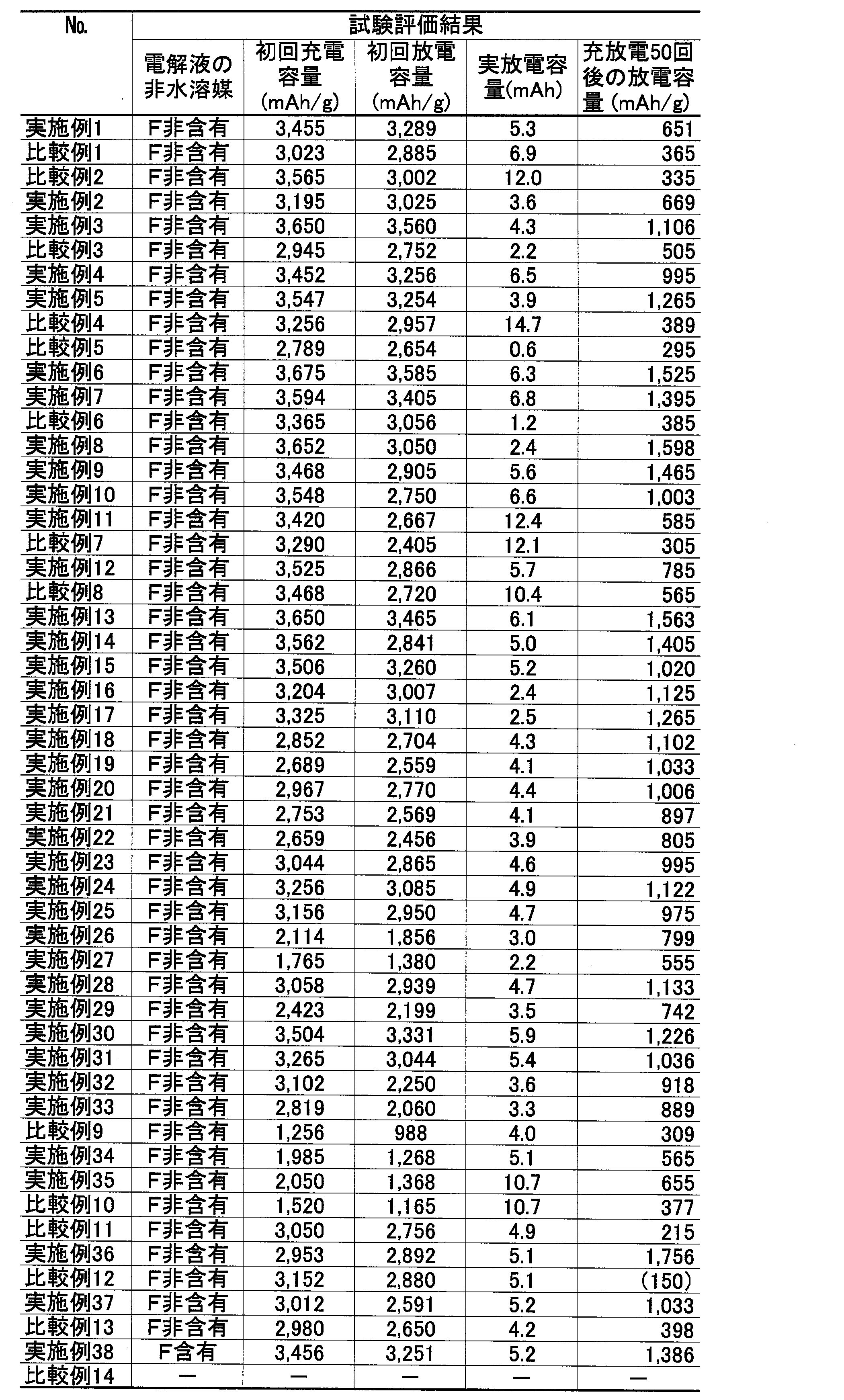
各試料の初回充電容量、放電容量、並びに50サイクル後の放電容量を比較すると、各実施例による試料の充放電特性が良好であることが判る。例えば、圧延銅箔を用いた実施例1と比較例1では、集電体の表面粗さRzが1.5μmと小さい比較例1では、集電体表面の実面積と凹凸が不充分なことから集電体表面明度が高くなって、50サイクル後の容量が400mAh/gを割る結果になっている。活物質の充放電繰り返しの体積膨張収縮による集電性等の劣化を生じたものとみられる。所定内の集電体表面の粗さと明度を有する実施例1では、600mAh/g以上の50サイクル後の放電容量を示す。他方、同じ両面光沢箔の電解箔を用いた比較例2と実施例2は、集電体の表面粗さまたは明度が規定値から外れているが、皮膜形成後の活物質皮膜の明度が規定外の比較例2では、サイクル試験後400mAh/gを割るが、活物質皮膜の明度が規定内に入る実施例2は600mAh/gを越える容量を維持する。実施例3は集電体表面のRzは4.7μmで、集電体と皮膜表面の明度が規定内に入る実施例3では、50サイクル後放電容量が1000mAh/g以上となっている。他方、集電体Rzが5.4μmで、1μmSi皮膜形成後の明度が規定の50を超える比較例3は初期容量が低くなり、サイクル後の容量も600mAh/gを下回っている。しかし、明度が規定内の実施例4~5では1千mAh/g前後を保持する容量を示した。また、集電体は規定を満たすものの、活物質皮膜が規定厚さを超えるか、規定厚さに満たない皮膜形成の比較例4~5では、明度が規定を超えるか、皮膜が薄すぎることにより、50サイクル容量が低く、しかも比較例5は実放電容量が低すぎて、実用に不向きであった。実施例6~7は規定内仕様により良好であるが、比較例6は明度値に満たないことから低いサイクル容量を示した。
2 耐熱性層と防錆処理層またはシランカップリング処理層
3 シリコン系活物質皮膜
4 粗化処理により粗面化した銅系微細粒子
5 集電体銅箔基材(両面平滑箔または光沢箔)
Claims (18)
- 銅箔または銅合金箔を用いた集電体の片面または両面に、シリコン系活物質皮膜が形成されている、非水電解質を用いる2次電池用の負極であって、
前記集電体上に、1g/m2~14g/m2のシリコン系活物質皮膜が形成され、
前記シリコン系活物質皮膜が形成された負極表面のXYZ表色系(CIE1931標準表色系)における明度Y値が15~50であり、かつ日本工業規格(JIS B0601-1994 十点平均粗さ)で規定される表面粗さ(十点平均粗さ)Rzが1.0μm以上4.5μm以下であることを特徴とする2次電池用負極。 - 前記シリコン系活物質皮膜は、リンおよび/または酸素を含有することを特徴とする、請求項1に記載の2次電池用負極。
- 前記シリコン系活物質皮膜は、さらに水素を含有することを特徴とする請求項1に記載の2次電池用負極。
- 前記集電体の前記シリコン系活物質皮膜の形成される表面上に、ニッケルを0.01~0.2g/m2含有する層または亜鉛を0.003~0.05g/m2含有する層の少なくとも一方が形成された耐熱性層を有することを特徴とする、請求項1に記載の2次電池用負極。
- さらに前記耐熱性層の上層に防錆層および/またはシランカップリング処理層が形成され、さらにその上層に前記シリコン系活物質皮膜が形成されていることを特徴とする請求項4に記載の2次電池用負極。
- 前記耐熱性層における亜鉛が、前記集電体、前記ニッケル層または前記シリコン系活物質皮膜に拡散していることを特徴とする、請求項4に記載の2次電池用負極。
- 銅箔または銅合金箔製であり、
片面または両面にシリコン系活物質皮膜が形成される、非水電解質を用いる2次電池用負極用の集電体であって、
前記集電体の引っ張り強度が300MPa以上1000MPa以下であり、
前記活物質皮膜が形成される表面の、XYZ表色系(CIE1931標準表色系)における明度Y値が10~40であり、
前記活物質皮膜が形成される表面の、日本工業規格(JIS B0601-1994 十点平均粗さ)で規定される表面粗さ(十点平均粗さ)Rzが2.0μm以上5.0μm以下である
ことを特徴とする2次電池用負極集電体。 - 銅箔または銅合金箔製であり、
片面または両面に、微粒子状の活物質をスラリー塗工により固化形成したシリコン系活物質層が形成される、非水電解質を用いる2次電池用負極用の集電体であって、
前記集電体の引っ張り強度が300MPa以上1000MPa以下であり、
前記活物質層が形成される表面の、XYZ表色系(CIE1931標準表色系)における明度Y値が20~50であり、
前記活物質層が形成される表面の、日本工業規格(JIS B0601-1994 十点平均粗さ)で規定される表面粗さ(十点平均粗さ)Rzが0.6μm以上3.5μm以下である
ことを特徴とする2次電池用負極集電体。 - 前記集電体の活物質皮膜形成面上に、ニッケルを0.01~0.2g/m2含有する層または亜鉛を0.003~0.05g/m2含有する層の少なくとも一方が形成された耐熱性層を有することを特徴とする、請求項7または8に記載の2次電池用負極集電体。
- さらに前記耐熱性層の上層に防錆層および/またはシランカップリング処理層を有することを特徴とする請求項9に記載の負極集電体。
- 請求項1に記載の負極または、請求項7もしくは8に記載の負極集電体を用いたことを特徴とする、非水電解質を用いた2次電池。
- 前記非水電解質にフッ素を含む非水溶媒を含有する電解液を用いることを特徴とする請求項11に記載の2次電池。
- 請求項7または8に記載の負極集電体の片面または両面に、シリコン系の活物質皮膜または活物質層を形成する、非水電解質を用いる2次電池用負極の製造方法であって、
前記負極集電体上に少なくともシリコンまたは、シリコンとリン、酸素もしくは水素を含むシリコン系の活物質皮膜または活物質層を、1g/m2~14g/m2となるように形成する工程を有することを特徴とする2次電池用負極の製造方法。 - 前記シリコン系活物質皮膜が、CVD(化学的気相成長)法、EB(電子ビーム)蒸着法またはスパッタリング法によって形成され、
前記シリコン系活物質層が、スラリー塗布・焼成法によって形成されることを特徴とする請求項13に記載の2次電池用負極の製造方法。 - 前記シリコン系活物質皮膜が形成された負極表面のXYZ表色系(CIE1931標準表色系)における明度Y値が15~50であり、かつ日本工業規格(JIS B0601-1994 十点平均粗さ)で規定される表面粗さ(十点平均粗さ)Rzが1.0μm以上4.5μm以下であることを特徴とする請求項13に記載の2次電池用負極の製造方法。
- 請求項7または8に記載の、非水電解質を用いる2次電池用負極集電体の製造方法であって、
引っ張り強度が300MPa以上1000MPa以下である集電体基材用銅箔の活物質形成面に、電気めっきを施して粗面形状を得る工程と、
を備えることを特徴とする、2次電池用負極集電体の製造方法。 - 粗面化した前記活物質形成面上に、少なくともニッケルまたは亜鉛を有する耐熱性層を形成することを特徴とする請求項16に記載の2次電池用負極集電体の製造方法。
- 前記耐熱性層上に、さらに防錆層および/またはシランカップリング層を形成することを特徴とする請求項17に記載の2次電池用負極集電体の製造方法。
Priority Applications (3)
| Application Number | Priority Date | Filing Date | Title |
|---|---|---|---|
| CN201180009749.7A CN102763246B (zh) | 2010-06-30 | 2011-06-27 | 二次电池用负极、负极集电体、它们的制造方法、以及二次电池 |
| KR1020127033852A KR101555090B1 (ko) | 2010-06-30 | 2011-06-27 | 2차 전지용 음극, 음극집전체 및 이의 제조 방법, 및 2차 전지 |
| US13/729,470 US9293771B2 (en) | 2010-06-30 | 2012-12-28 | Anode for secondary battery, anode current collector, production method thereof, and secondary battery |
Applications Claiming Priority (2)
| Application Number | Priority Date | Filing Date | Title |
|---|---|---|---|
| JP2010148612A JP5666839B2 (ja) | 2010-06-30 | 2010-06-30 | 2次電池用負極、負極集電体、2次電池及びこれらの製造方法 |
| JP2010-148612 | 2010-06-30 |
Related Child Applications (1)
| Application Number | Title | Priority Date | Filing Date |
|---|---|---|---|
| US13/729,470 Continuation US9293771B2 (en) | 2010-06-30 | 2012-12-28 | Anode for secondary battery, anode current collector, production method thereof, and secondary battery |
Publications (1)
| Publication Number | Publication Date |
|---|---|
| WO2012002304A1 true WO2012002304A1 (ja) | 2012-01-05 |
Family
ID=45402017
Family Applications (1)
| Application Number | Title | Priority Date | Filing Date |
|---|---|---|---|
| PCT/JP2011/064632 Ceased WO2012002304A1 (ja) | 2010-06-30 | 2011-06-27 | 2次電池用負極、負極集電体及びこれらの製造方法、並びに2次電池 |
Country Status (6)
| Country | Link |
|---|---|
| US (1) | US9293771B2 (ja) |
| JP (1) | JP5666839B2 (ja) |
| KR (1) | KR101555090B1 (ja) |
| CN (1) | CN102763246B (ja) |
| TW (1) | TWI443897B (ja) |
| WO (1) | WO2012002304A1 (ja) |
Cited By (3)
| Publication number | Priority date | Publication date | Assignee | Title |
|---|---|---|---|---|
| US20150132658A1 (en) * | 2012-05-22 | 2015-05-14 | Mitsui Mining & Smelting Co., Ltd. | Copper foil, negative electrode current collector and negative electrode material for non-aqueous secondary battery |
| US11569526B2 (en) * | 2019-05-03 | 2023-01-31 | Hyundai Motor Company | High energy density all-solid-state battery and method for manufacturing the same |
| US12489109B2 (en) | 2019-08-14 | 2025-12-02 | Leydenjar Technologies B.V. | Silicon composition material for use as battery anode |
Families Citing this family (44)
| Publication number | Priority date | Publication date | Assignee | Title |
|---|---|---|---|---|
| JP5621868B2 (ja) * | 2012-03-27 | 2014-11-12 | Tdk株式会社 | リチウムイオン二次電池 |
| JP6030401B2 (ja) * | 2012-10-12 | 2016-11-24 | 三井金属鉱業株式会社 | 表面処理銅箔の製造方法 |
| JP2015064988A (ja) | 2013-09-24 | 2015-04-09 | 株式会社東芝 | 非水電解質二次電池及び電池パック |
| CN103928658B (zh) * | 2013-12-30 | 2016-06-29 | 福建省诺希新材料科技有限公司 | 一种石墨烯/硅复合阳极材料的制备方法及制品 |
| JP6172083B2 (ja) * | 2014-08-04 | 2017-08-02 | トヨタ自動車株式会社 | リチウム固体二次電池およびその製造方法 |
| TW201622228A (zh) * | 2014-08-27 | 2016-06-16 | 應用材料股份有限公司 | 三維薄膜電池 |
| CN107004890B (zh) * | 2014-12-26 | 2020-12-25 | 积水化学工业株式会社 | 电极制造方法、电极和二次电池 |
| KR102130011B1 (ko) * | 2015-06-23 | 2020-07-03 | 케이씨에프테크놀로지스 주식회사 | 리튬 이차전지용 전해동박 및 이를 포함하는 리튬 이차전지 |
| US9397343B1 (en) | 2015-10-15 | 2016-07-19 | Chang Chun Petrochemical Co., Ltd. | Copper foil exhibiting anti-swelling properties |
| DE102015120879A1 (de) * | 2015-12-02 | 2017-06-08 | Institut Für Solarenergieforschung Gmbh | Verfahren zum Herstellen einer Silizium-basierten porösen Elektrode für eine Batterie, insbesondere Lithium-Ionen-Batterie |
| US20190312282A1 (en) * | 2016-12-02 | 2019-10-10 | Nissan Chemical Corporation | Thin film, and undercoat foil for energy storage device electrode |
| CN106960960A (zh) * | 2017-05-11 | 2017-07-18 | 天津理工大学 | 一种提高锂离子电池负极材的循环性能的柔性集流体的制备方法 |
| WO2018224334A1 (en) * | 2017-06-09 | 2018-12-13 | Robert Bosch Gmbh | Battery cell with anode protective layer |
| KR102473030B1 (ko) * | 2017-08-30 | 2022-11-30 | 에스케이넥실리스 주식회사 | 전해동박, 그의 제조방법 및 그것을 포함하는 고용량 Li 이차전지용 음극 |
| DE102017219895A1 (de) * | 2017-11-09 | 2019-05-09 | Bayerische Motoren Werke Aktiengesellschaft | Verfahren zum Integrieren eines Hochvoltspeichers in eine Tragstruktur eines Kraftfahrzeugs sowie Kraftfahrzeug |
| US10424793B2 (en) * | 2017-11-14 | 2019-09-24 | Chang Chun Petrochemical Co., Ltd. | Electrodeposited copper foil and method for producing the same, and current collector for lithium secondary battery and secondary battery comprising the electrodeposited copper foil |
| EP4629381A3 (en) | 2018-02-26 | 2025-10-15 | Graphenix Development, Inc. | Anodes for lithium-based energy storage devices |
| CN111048767A (zh) * | 2018-10-11 | 2020-04-21 | 上海汽车集团股份有限公司 | 一种电池负极及其制备方法 |
| CN111058063B (zh) * | 2018-10-16 | 2021-02-02 | 长春石油化学股份有限公司 | 电解铜箔、包含其的电极、及包含其的锂离子电池 |
| US11365486B2 (en) | 2018-10-16 | 2022-06-21 | Chang Chun Petrochemical Co., Ltd. | Electrolytic copper foil, electrode comprising the same, and lithium ion battery comprising the same |
| KR20200102242A (ko) * | 2019-02-21 | 2020-08-31 | 에스케이이노베이션 주식회사 | 전극용 기재 및 이를 이용한 전극 제조 방법 |
| JP6726780B1 (ja) * | 2019-03-04 | 2020-07-22 | ナミックス株式会社 | 銅箔並びにそれを含むリチウムイオン電池の負極集電体及びその製造方法 |
| US11024842B2 (en) | 2019-06-27 | 2021-06-01 | Graphenix Development, Inc. | Patterned anodes for lithium-based energy storage devices |
| US11437624B2 (en) | 2019-08-13 | 2022-09-06 | Graphenix Development, Inc. | Anodes for lithium-based energy storage devices, and methods for making same |
| CA3148530A1 (en) | 2019-08-20 | 2021-02-25 | Graphenix Development, Inc. | Structured anodes for lithium-based energy storage devices |
| US11489154B2 (en) | 2019-08-20 | 2022-11-01 | Graphenix Development, Inc. | Multilayer anodes for lithium-based energy storage devices |
| US11495782B2 (en) | 2019-08-26 | 2022-11-08 | Graphenix Development, Inc. | Asymmetric anodes for lithium-based energy storage devices |
| TWI700393B (zh) | 2019-08-27 | 2020-08-01 | 長春石油化學股份有限公司 | 電解銅箔以及包含其之電極與鋰離子電池 |
| KR102774325B1 (ko) * | 2019-11-20 | 2025-03-05 | 주식회사 엘지에너지솔루션 | 전극 리드 제조 방법 및 파우치 형 이차 전지 |
| WO2021097815A1 (zh) * | 2019-11-22 | 2021-05-27 | 宁德新能源科技有限公司 | 电池及用电装置 |
| KR102971556B1 (ko) * | 2019-12-03 | 2026-06-04 | 사이언스코 | 플루오린화 어사이클릭 카르보네이트 및 플루오린화 사이클릭 카르보네이트를 함유하는 전해질 조성물 |
| PL3965201T3 (pl) * | 2020-03-27 | 2023-08-21 | Contemporary Amperex Technology Co., Limited | Akumulator i zawierające go urządzenie |
| FR3109024A1 (fr) * | 2020-04-01 | 2021-10-08 | Armor | Anode au silicium pour accumulateur électrochimique |
| WO2021207357A1 (en) | 2020-04-08 | 2021-10-14 | Graphenix Development, Inc. | Anodes for lithium-based energy storage devices |
| WO2022005999A1 (en) | 2020-06-29 | 2022-01-06 | Graphenix Development, Inc. | Anodes for lithium-based energy storage devices |
| CN111682200B (zh) * | 2020-07-14 | 2021-10-22 | 万华化学集团股份有限公司 | 用于锂离子电池的正极材料及其制备方法 |
| US12255315B2 (en) | 2021-01-14 | 2025-03-18 | Graphenix Development, Inc. | Anode structures having a multiple supplemental layers |
| US12388067B2 (en) | 2021-04-26 | 2025-08-12 | Graphenix Development, Inc. | Anodes for lithium-based energy storage devices |
| KR102772353B1 (ko) * | 2021-10-12 | 2025-02-26 | 주식회사 엘지에너지솔루션 | 이차전지용 음극 및 이를 포함하는 젤리-롤형 전극 조립체 |
| NL2029989B1 (en) | 2021-12-01 | 2023-06-19 | Leydenjar Tech B V | Composite electrode material, method for its production and use of the material |
| JP7811107B2 (ja) * | 2021-12-07 | 2026-02-04 | 三菱鉛筆株式会社 | 二次電池負極電極用水系スラリーの製造方法 |
| KR20240133741A (ko) * | 2022-01-14 | 2024-09-04 | 에볼로 인코포레이티드 | 수전해조용 확장 가능한 전극 유로 및 이의 고속 제조 방법 |
| CN116804294A (zh) * | 2022-03-16 | 2023-09-26 | 华中科技大学 | 一种锌氮共掺杂海绵状多孔碳纤维材料的制备方法及其应用 |
| CN118398894B (zh) * | 2024-04-11 | 2025-10-17 | 珠海冠宇电池股份有限公司 | 一种电化学装置 |
Citations (8)
| Publication number | Priority date | Publication date | Assignee | Title |
|---|---|---|---|---|
| JP2001015100A (ja) * | 1999-06-29 | 2001-01-19 | Fujitsu Ltd | 電池用電極の製造方法及び電池 |
| JP2002319408A (ja) * | 2001-04-23 | 2002-10-31 | Sanyo Electric Co Ltd | リチウム二次電池用電極及びリチウム二次電池 |
| JP3935067B2 (ja) * | 2002-12-26 | 2007-06-20 | ソニー株式会社 | 二次電池用負極およびそれを用いた二次電池 |
| JP2008010320A (ja) * | 2006-06-29 | 2008-01-17 | Sony Corp | 電極集電体及びその検査方法、電池用電極及びその製造方法、並びに二次電池及びその製造方法 |
| JP2009110846A (ja) * | 2007-10-31 | 2009-05-21 | Sony Corp | 負極活物質、負極および電池 |
| JP2010103006A (ja) * | 2008-10-24 | 2010-05-06 | Sony Corp | 負極集電体、負極および二次電池 |
| JP2010182620A (ja) * | 2009-02-09 | 2010-08-19 | Panasonic Corp | リチウムイオン二次電池 |
| WO2010128681A1 (ja) * | 2009-05-08 | 2010-11-11 | 古河電気工業株式会社 | 2次電池用負極、電極用銅箔、2次電池および2次電池用負極の製造方法 |
Family Cites Families (10)
| Publication number | Priority date | Publication date | Assignee | Title |
|---|---|---|---|---|
| JP3581784B2 (ja) | 1998-03-19 | 2004-10-27 | 古河電気工業株式会社 | 非水溶媒二次電池の負極集電体用銅箔 |
| TW515124B (en) | 1999-10-22 | 2002-12-21 | Sanyo Electric Co | Electrode for a lithium battery and a lithium secondary battery |
| AU2001227022A1 (en) | 2000-01-18 | 2001-07-31 | Ramot University Authority For Applied Research And Industrial Development Ltd. | Fuel cell with proton conducting membrane |
| CN100377404C (zh) * | 2000-11-16 | 2008-03-26 | 三菱综合材料株式会社 | 固体电解质型燃料电池及其上使用的空气极集电体 |
| US6887623B2 (en) | 2001-04-09 | 2005-05-03 | Sanyo Electric Co., Ltd. | Electrode for rechargeable lithium battery and rechargeable lithium battery |
| CN1320672C (zh) * | 2005-07-25 | 2007-06-06 | 北京中科天华科技发展有限公司 | 一种适用于锂离子电池的纳米电解铜箔的制备方法 |
| CN100580980C (zh) | 2007-02-16 | 2010-01-13 | 索尼株式会社 | 负极、其制造方法以及电池 |
| JP5251024B2 (ja) | 2007-07-26 | 2013-07-31 | ソニー株式会社 | リチウムイオン二次電池用負極およびリチウムイオン二次電池 |
| JP2010097843A (ja) * | 2008-10-17 | 2010-04-30 | Panasonic Corp | リチウムイオン二次電池 |
| JPWO2011052605A1 (ja) | 2009-10-27 | 2013-03-21 | 旭硝子株式会社 | 二次電池用非水電解液および二次電池 |
-
2010
- 2010-06-30 JP JP2010148612A patent/JP5666839B2/ja not_active Expired - Fee Related
-
2011
- 2011-06-27 WO PCT/JP2011/064632 patent/WO2012002304A1/ja not_active Ceased
- 2011-06-27 CN CN201180009749.7A patent/CN102763246B/zh not_active Expired - Fee Related
- 2011-06-27 KR KR1020127033852A patent/KR101555090B1/ko not_active Expired - Fee Related
- 2011-06-29 TW TW100122832A patent/TWI443897B/zh not_active IP Right Cessation
-
2012
- 2012-12-28 US US13/729,470 patent/US9293771B2/en not_active Expired - Fee Related
Patent Citations (8)
| Publication number | Priority date | Publication date | Assignee | Title |
|---|---|---|---|---|
| JP2001015100A (ja) * | 1999-06-29 | 2001-01-19 | Fujitsu Ltd | 電池用電極の製造方法及び電池 |
| JP2002319408A (ja) * | 2001-04-23 | 2002-10-31 | Sanyo Electric Co Ltd | リチウム二次電池用電極及びリチウム二次電池 |
| JP3935067B2 (ja) * | 2002-12-26 | 2007-06-20 | ソニー株式会社 | 二次電池用負極およびそれを用いた二次電池 |
| JP2008010320A (ja) * | 2006-06-29 | 2008-01-17 | Sony Corp | 電極集電体及びその検査方法、電池用電極及びその製造方法、並びに二次電池及びその製造方法 |
| JP2009110846A (ja) * | 2007-10-31 | 2009-05-21 | Sony Corp | 負極活物質、負極および電池 |
| JP2010103006A (ja) * | 2008-10-24 | 2010-05-06 | Sony Corp | 負極集電体、負極および二次電池 |
| JP2010182620A (ja) * | 2009-02-09 | 2010-08-19 | Panasonic Corp | リチウムイオン二次電池 |
| WO2010128681A1 (ja) * | 2009-05-08 | 2010-11-11 | 古河電気工業株式会社 | 2次電池用負極、電極用銅箔、2次電池および2次電池用負極の製造方法 |
Cited By (4)
| Publication number | Priority date | Publication date | Assignee | Title |
|---|---|---|---|---|
| US20150132658A1 (en) * | 2012-05-22 | 2015-05-14 | Mitsui Mining & Smelting Co., Ltd. | Copper foil, negative electrode current collector and negative electrode material for non-aqueous secondary battery |
| US10396363B2 (en) * | 2012-05-22 | 2019-08-27 | Mitsui Mining & Smelting Co., Ltd. | Copper foil, negative electrode current collector and negative electrode material for non-aqueous secondary battery |
| US11569526B2 (en) * | 2019-05-03 | 2023-01-31 | Hyundai Motor Company | High energy density all-solid-state battery and method for manufacturing the same |
| US12489109B2 (en) | 2019-08-14 | 2025-12-02 | Leydenjar Technologies B.V. | Silicon composition material for use as battery anode |
Also Published As
| Publication number | Publication date |
|---|---|
| KR20130031301A (ko) | 2013-03-28 |
| US9293771B2 (en) | 2016-03-22 |
| TW201212361A (en) | 2012-03-16 |
| JP2012014895A (ja) | 2012-01-19 |
| CN102763246A (zh) | 2012-10-31 |
| CN102763246B (zh) | 2015-04-08 |
| KR101555090B1 (ko) | 2015-09-22 |
| US20130115510A1 (en) | 2013-05-09 |
| TWI443897B (zh) | 2014-07-01 |
| JP5666839B2 (ja) | 2015-02-12 |
Similar Documents
| Publication | Publication Date | Title |
|---|---|---|
| JP5666839B2 (ja) | 2次電池用負極、負極集電体、2次電池及びこれらの製造方法 | |
| KR101346956B1 (ko) | 2차 전지용 음극, 전극용 동박, 2차 전지 및 2차 전지용 음극의 제조방법 | |
| JP5356309B2 (ja) | 2次電池用負極、電極用銅箔、2次電池および2次電池用負極の製造方法 | |
| JP5119277B2 (ja) | リチウム二次電池用電極及びその製造方法 | |
| JP2022544754A (ja) | バッテリーアノードとして使用するためのケイ素組成物材料 | |
| TWI684651B (zh) | 電解銅箔、用於製造其的方法以及用於高容量的鋰二次電池的陽極 | |
| WO2012005355A1 (ja) | 銅被覆鋼箔、負極集電体及びその製法並びに電池 | |
| CN101512797A (zh) | 负极活性物质、负极和锂二次电池 | |
| JP5437155B2 (ja) | 2次電池用負極、電極用銅箔、2次電池および2次電池用負極の製造方法 | |
| JP5437536B2 (ja) | 電極用集電体、非水電解質二次電池用負極、非水電解質二次電池 | |
| CN108270016A (zh) | 电解铜箔、电极、二次电池及其制造方法 | |
| TW201312839A (zh) | 鋰離子二次電池負極材之製造方法及鋰離子二次電池用負極材 | |
| Yoon et al. | Crater-like architectural aluminum current collectors with superior electrochemical performance for Li-ion batteries | |
| Jeong et al. | Embossed aluminum as a current collector for high-rate lithium cathode performance | |
| JP2010043333A (ja) | 正極集電体用アルミニウム箔 | |
| JP5356308B2 (ja) | 2次電池用負極、電極用銅箔、2次電池および2次電池用負極の製造方法 | |
| JP2010027304A (ja) | 正極集電体用アルミニウム箔 | |
| US9871254B2 (en) | Electrode material and manufacturing method thereof | |
| Yang et al. | Study on the influence of copper foil current collector roughness on lithium-ion battery performance | |
| JP6495009B2 (ja) | 二次電池用正極、二次電池および二次電池用正極の製造方法 | |
| JP5873711B2 (ja) | 銅箔、二次電池の電極、二次電池、並びにプリント回路基板 | |
| JP2012178309A (ja) | リチウムイオン二次電池用負極と、これを用いたリチウムイオン二次電池 | |
| JP2009295470A (ja) | リチウムイオン二次電池 | |
| JP2018174075A (ja) | リチウムイオン電池集電体用圧延銅箔及びリチウムイオン電池 | |
| JP5211660B2 (ja) | 全固体リチウム二次電池の製造方法 |
Legal Events
| Date | Code | Title | Description |
|---|---|---|---|
| WWE | Wipo information: entry into national phase |
Ref document number: 201180009749.7 Country of ref document: CN |
|
| 121 | Ep: the epo has been informed by wipo that ep was designated in this application |
Ref document number: 11800768 Country of ref document: EP Kind code of ref document: A1 |
|
| ENP | Entry into the national phase |
Ref document number: 20127033852 Country of ref document: KR Kind code of ref document: A |
|
| NENP | Non-entry into the national phase |
Ref country code: DE |
|
| 122 | Ep: pct application non-entry in european phase |
Ref document number: 11800768 Country of ref document: EP Kind code of ref document: A1 |