US9461220B2 - Resin-attached lead frame, method for manufacturing the same, and lead frame - Google Patents
Resin-attached lead frame, method for manufacturing the same, and lead frame Download PDFInfo
- Publication number
- US9461220B2 US9461220B2 US13/980,980 US201213980980A US9461220B2 US 9461220 B2 US9461220 B2 US 9461220B2 US 201213980980 A US201213980980 A US 201213980980A US 9461220 B2 US9461220 B2 US 9461220B2
- Authority
- US
- United States
- Prior art keywords
- lead frame
- aluminum layer
- led element
- tie bar
- main body
- Prior art date
- Legal status (The legal status is an assumption and is not a legal conclusion. Google has not performed a legal analysis and makes no representation as to the accuracy of the status listed.)
- Active, expires
Links
- 238000000034 method Methods 0.000 title claims description 22
- 238000004519 manufacturing process Methods 0.000 title claims description 19
- 229910052782 aluminium Inorganic materials 0.000 claims abstract description 166
- XAGFODPZIPBFFR-UHFFFAOYSA-N aluminium Chemical compound [Al] XAGFODPZIPBFFR-UHFFFAOYSA-N 0.000 claims abstract description 166
- 229920005989 resin Polymers 0.000 claims abstract description 111
- 239000011347 resin Substances 0.000 claims abstract description 111
- 230000000284 resting effect Effects 0.000 claims abstract description 91
- RYGMFSIKBFXOCR-UHFFFAOYSA-N Copper Chemical compound [Cu] RYGMFSIKBFXOCR-UHFFFAOYSA-N 0.000 claims description 10
- 229910052802 copper Inorganic materials 0.000 claims description 10
- 239000010949 copper Substances 0.000 claims description 10
- 229910045601 alloy Inorganic materials 0.000 claims description 5
- 239000000956 alloy Substances 0.000 claims description 5
- 230000002708 enhancing effect Effects 0.000 claims description 5
- 229910000881 Cu alloy Inorganic materials 0.000 claims description 4
- 239000004065 semiconductor Substances 0.000 description 39
- 239000000758 substrate Substances 0.000 description 20
- 239000000463 material Substances 0.000 description 14
- 238000007789 sealing Methods 0.000 description 14
- BQCADISMDOOEFD-UHFFFAOYSA-N Silver Chemical compound [Ag] BQCADISMDOOEFD-UHFFFAOYSA-N 0.000 description 11
- 238000012986 modification Methods 0.000 description 11
- 230000004048 modification Effects 0.000 description 11
- 229910052709 silver Inorganic materials 0.000 description 11
- 239000004332 silver Substances 0.000 description 11
- 238000000605 extraction Methods 0.000 description 9
- 229910000679 solder Inorganic materials 0.000 description 8
- 238000005286 illumination Methods 0.000 description 7
- KDLHZDBZIXYQEI-UHFFFAOYSA-N Palladium Chemical compound [Pd] KDLHZDBZIXYQEI-UHFFFAOYSA-N 0.000 description 6
- 230000000593 degrading effect Effects 0.000 description 6
- 238000005530 etching Methods 0.000 description 6
- BASFCYQUMIYNBI-UHFFFAOYSA-N platinum Chemical compound [Pt] BASFCYQUMIYNBI-UHFFFAOYSA-N 0.000 description 6
- 239000000126 substance Substances 0.000 description 6
- 239000004954 Polyphthalamide Substances 0.000 description 5
- 238000001746 injection moulding Methods 0.000 description 5
- 238000007747 plating Methods 0.000 description 5
- 229920006375 polyphtalamide Polymers 0.000 description 5
- 238000004544 sputter deposition Methods 0.000 description 5
- 239000004593 Epoxy Substances 0.000 description 4
- 229920001187 thermosetting polymer Polymers 0.000 description 4
- 238000001721 transfer moulding Methods 0.000 description 4
- 238000009713 electroplating Methods 0.000 description 3
- 229910052751 metal Inorganic materials 0.000 description 3
- 239000002184 metal Substances 0.000 description 3
- 229910052763 palladium Inorganic materials 0.000 description 3
- 229910052697 platinum Inorganic materials 0.000 description 3
- 229920000647 polyepoxide Polymers 0.000 description 3
- 229910052703 rhodium Inorganic materials 0.000 description 3
- 239000010948 rhodium Substances 0.000 description 3
- MHOVAHRLVXNVSD-UHFFFAOYSA-N rhodium atom Chemical compound [Rh] MHOVAHRLVXNVSD-UHFFFAOYSA-N 0.000 description 3
- 229920002050 silicone resin Polymers 0.000 description 3
- 239000000243 solution Substances 0.000 description 3
- 229920005992 thermoplastic resin Polymers 0.000 description 3
- 238000007740 vapor deposition Methods 0.000 description 3
- RWSOTUBLDIXVET-UHFFFAOYSA-N Dihydrogen sulfide Chemical compound S RWSOTUBLDIXVET-UHFFFAOYSA-N 0.000 description 2
- 229910000640 Fe alloy Inorganic materials 0.000 description 2
- GWEVSGVZZGPLCZ-UHFFFAOYSA-N Titan oxide Chemical compound O=[Ti]=O GWEVSGVZZGPLCZ-UHFFFAOYSA-N 0.000 description 2
- 230000015572 biosynthetic process Effects 0.000 description 2
- 239000004020 conductor Substances 0.000 description 2
- 238000005520 cutting process Methods 0.000 description 2
- 238000005238 degreasing Methods 0.000 description 2
- 238000000151 deposition Methods 0.000 description 2
- 238000002845 discoloration Methods 0.000 description 2
- 230000000694 effects Effects 0.000 description 2
- 239000003822 epoxy resin Substances 0.000 description 2
- PCHJSUWPFVWCPO-UHFFFAOYSA-N gold Chemical compound [Au] PCHJSUWPFVWCPO-UHFFFAOYSA-N 0.000 description 2
- 229910052737 gold Inorganic materials 0.000 description 2
- 239000010931 gold Substances 0.000 description 2
- 229910000037 hydrogen sulfide Inorganic materials 0.000 description 2
- 239000013528 metallic particle Substances 0.000 description 2
- 229910052759 nickel Inorganic materials 0.000 description 2
- 230000003287 optical effect Effects 0.000 description 2
- 238000004806 packaging method and process Methods 0.000 description 2
- 230000005855 radiation Effects 0.000 description 2
- 230000003746 surface roughness Effects 0.000 description 2
- 229920003002 synthetic resin Polymers 0.000 description 2
- 239000000057 synthetic resin Substances 0.000 description 2
- 238000005406 washing Methods 0.000 description 2
- XLYOFNOQVPJJNP-UHFFFAOYSA-N water Substances O XLYOFNOQVPJJNP-UHFFFAOYSA-N 0.000 description 2
- 229910052582 BN Inorganic materials 0.000 description 1
- PZNSFCLAULLKQX-UHFFFAOYSA-N Boron nitride Chemical compound N#B PZNSFCLAULLKQX-UHFFFAOYSA-N 0.000 description 1
- XFXPMWWXUTWYJX-UHFFFAOYSA-N Cyanide Chemical compound N#[C-] XFXPMWWXUTWYJX-UHFFFAOYSA-N 0.000 description 1
- 229910001218 Gallium arsenide Inorganic materials 0.000 description 1
- 229910021578 Iron(III) chloride Inorganic materials 0.000 description 1
- 229920000106 Liquid crystal polymer Polymers 0.000 description 1
- 239000004977 Liquid-crystal polymers (LCPs) Substances 0.000 description 1
- 239000004952 Polyamide Substances 0.000 description 1
- 239000004697 Polyetherimide Substances 0.000 description 1
- 239000004642 Polyimide Substances 0.000 description 1
- 239000004721 Polyphenylene oxide Substances 0.000 description 1
- 239000004734 Polyphenylene sulfide Substances 0.000 description 1
- MCMNRKCIXSYSNV-UHFFFAOYSA-N ZrO2 Inorganic materials O=[Zr]=O MCMNRKCIXSYSNV-UHFFFAOYSA-N 0.000 description 1
- 230000003213 activating effect Effects 0.000 description 1
- 230000015556 catabolic process Effects 0.000 description 1
- 230000001413 cellular effect Effects 0.000 description 1
- 239000000919 ceramic Substances 0.000 description 1
- 238000006243 chemical reaction Methods 0.000 description 1
- 239000003795 chemical substances by application Substances 0.000 description 1
- 238000004140 cleaning Methods 0.000 description 1
- 150000001875 compounds Chemical class 0.000 description 1
- PMHQVHHXPFUNSP-UHFFFAOYSA-M copper(1+);methylsulfanylmethane;bromide Chemical compound Br[Cu].CSC PMHQVHHXPFUNSP-UHFFFAOYSA-M 0.000 description 1
- 239000013078 crystal Substances 0.000 description 1
- 230000003247 decreasing effect Effects 0.000 description 1
- 238000006731 degradation reaction Methods 0.000 description 1
- 230000008021 deposition Effects 0.000 description 1
- 230000006866 deterioration Effects 0.000 description 1
- 229910003460 diamond Inorganic materials 0.000 description 1
- 239000010432 diamond Substances 0.000 description 1
- NJLLQSBAHIKGKF-UHFFFAOYSA-N dipotassium dioxido(oxo)titanium Chemical compound [K+].[K+].[O-][Ti]([O-])=O NJLLQSBAHIKGKF-UHFFFAOYSA-N 0.000 description 1
- 238000005516 engineering process Methods 0.000 description 1
- 125000003700 epoxy group Chemical group 0.000 description 1
- 230000004907 flux Effects 0.000 description 1
- 239000011521 glass Substances 0.000 description 1
- 238000000227 grinding Methods 0.000 description 1
- RBTARNINKXHZNM-UHFFFAOYSA-K iron trichloride Chemical compound Cl[Fe](Cl)Cl RBTARNINKXHZNM-UHFFFAOYSA-K 0.000 description 1
- 239000004973 liquid crystal related substance Substances 0.000 description 1
- 230000007935 neutral effect Effects 0.000 description 1
- RVTZCBVAJQQJTK-UHFFFAOYSA-N oxygen(2-);zirconium(4+) Chemical compound [O-2].[O-2].[Zr+4] RVTZCBVAJQQJTK-UHFFFAOYSA-N 0.000 description 1
- 238000005554 pickling Methods 0.000 description 1
- 238000005498 polishing Methods 0.000 description 1
- 229920002647 polyamide Polymers 0.000 description 1
- -1 polybutylene terephthalate Polymers 0.000 description 1
- 229920001707 polybutylene terephthalate Polymers 0.000 description 1
- 229920000570 polyether Polymers 0.000 description 1
- 229920001601 polyetherimide Polymers 0.000 description 1
- 229920001721 polyimide Polymers 0.000 description 1
- 229920000098 polyolefin Polymers 0.000 description 1
- 229920000069 polyphenylene sulfide Polymers 0.000 description 1
- 229920001296 polysiloxane Polymers 0.000 description 1
- 238000005096 rolling process Methods 0.000 description 1
- LFAGQMCIGQNPJG-UHFFFAOYSA-N silver cyanide Chemical compound [Ag+].N#[C-] LFAGQMCIGQNPJG-UHFFFAOYSA-N 0.000 description 1
- 229940098221 silver cyanide Drugs 0.000 description 1
- 238000005476 soldering Methods 0.000 description 1
- 125000001174 sulfone group Chemical group 0.000 description 1
- 239000004408 titanium dioxide Substances 0.000 description 1
- 238000002834 transmittance Methods 0.000 description 1
- 239000011800 void material Substances 0.000 description 1
Images


Classifications
-
- H—ELECTRICITY
- H01—ELECTRIC ELEMENTS
- H01L—SEMICONDUCTOR DEVICES NOT COVERED BY CLASS H10
- H01L33/00—Semiconductor devices having potential barriers specially adapted for light emission; Processes or apparatus specially adapted for the manufacture or treatment thereof or of parts thereof; Details thereof
- H01L33/48—Semiconductor devices having potential barriers specially adapted for light emission; Processes or apparatus specially adapted for the manufacture or treatment thereof or of parts thereof; Details thereof characterised by the semiconductor body packages
- H01L33/52—Encapsulations
- H01L33/56—Materials, e.g. epoxy or silicone resin
-
- H—ELECTRICITY
- H01—ELECTRIC ELEMENTS
- H01L—SEMICONDUCTOR DEVICES NOT COVERED BY CLASS H10
- H01L33/00—Semiconductor devices having potential barriers specially adapted for light emission; Processes or apparatus specially adapted for the manufacture or treatment thereof or of parts thereof; Details thereof
- H01L33/48—Semiconductor devices having potential barriers specially adapted for light emission; Processes or apparatus specially adapted for the manufacture or treatment thereof or of parts thereof; Details thereof characterised by the semiconductor body packages
- H01L33/58—Optical field-shaping elements
- H01L33/60—Reflective elements
-
- H—ELECTRICITY
- H01—ELECTRIC ELEMENTS
- H01L—SEMICONDUCTOR DEVICES NOT COVERED BY CLASS H10
- H01L33/00—Semiconductor devices having potential barriers specially adapted for light emission; Processes or apparatus specially adapted for the manufacture or treatment thereof or of parts thereof; Details thereof
- H01L33/44—Semiconductor devices having potential barriers specially adapted for light emission; Processes or apparatus specially adapted for the manufacture or treatment thereof or of parts thereof; Details thereof characterised by the coatings, e.g. passivation layer or anti-reflective coating
- H01L33/46—Reflective coating, e.g. dielectric Bragg reflector
-
- H—ELECTRICITY
- H01—ELECTRIC ELEMENTS
- H01L—SEMICONDUCTOR DEVICES NOT COVERED BY CLASS H10
- H01L33/00—Semiconductor devices having potential barriers specially adapted for light emission; Processes or apparatus specially adapted for the manufacture or treatment thereof or of parts thereof; Details thereof
- H01L33/48—Semiconductor devices having potential barriers specially adapted for light emission; Processes or apparatus specially adapted for the manufacture or treatment thereof or of parts thereof; Details thereof characterised by the semiconductor body packages
- H01L33/483—Containers
- H01L33/486—Containers adapted for surface mounting
-
- H—ELECTRICITY
- H01—ELECTRIC ELEMENTS
- H01L—SEMICONDUCTOR DEVICES NOT COVERED BY CLASS H10
- H01L33/00—Semiconductor devices having potential barriers specially adapted for light emission; Processes or apparatus specially adapted for the manufacture or treatment thereof or of parts thereof; Details thereof
- H01L33/48—Semiconductor devices having potential barriers specially adapted for light emission; Processes or apparatus specially adapted for the manufacture or treatment thereof or of parts thereof; Details thereof characterised by the semiconductor body packages
- H01L33/62—Arrangements for conducting electric current to or from the semiconductor body, e.g. lead-frames, wire-bonds or solder balls
-
- H—ELECTRICITY
- H01—ELECTRIC ELEMENTS
- H01L—SEMICONDUCTOR DEVICES NOT COVERED BY CLASS H10
- H01L2224/00—Indexing scheme for arrangements for connecting or disconnecting semiconductor or solid-state bodies and methods related thereto as covered by H01L24/00
- H01L2224/01—Means for bonding being attached to, or being formed on, the surface to be connected, e.g. chip-to-package, die-attach, "first-level" interconnects; Manufacturing methods related thereto
- H01L2224/42—Wire connectors; Manufacturing methods related thereto
- H01L2224/47—Structure, shape, material or disposition of the wire connectors after the connecting process
- H01L2224/48—Structure, shape, material or disposition of the wire connectors after the connecting process of an individual wire connector
- H01L2224/4805—Shape
- H01L2224/4809—Loop shape
- H01L2224/48091—Arched
-
- H—ELECTRICITY
- H01—ELECTRIC ELEMENTS
- H01L—SEMICONDUCTOR DEVICES NOT COVERED BY CLASS H10
- H01L2224/00—Indexing scheme for arrangements for connecting or disconnecting semiconductor or solid-state bodies and methods related thereto as covered by H01L24/00
- H01L2224/01—Means for bonding being attached to, or being formed on, the surface to be connected, e.g. chip-to-package, die-attach, "first-level" interconnects; Manufacturing methods related thereto
- H01L2224/42—Wire connectors; Manufacturing methods related thereto
- H01L2224/47—Structure, shape, material or disposition of the wire connectors after the connecting process
- H01L2224/48—Structure, shape, material or disposition of the wire connectors after the connecting process of an individual wire connector
- H01L2224/481—Disposition
- H01L2224/48151—Connecting between a semiconductor or solid-state body and an item not being a semiconductor or solid-state body, e.g. chip-to-substrate, chip-to-passive
- H01L2224/48221—Connecting between a semiconductor or solid-state body and an item not being a semiconductor or solid-state body, e.g. chip-to-substrate, chip-to-passive the body and the item being stacked
- H01L2224/48245—Connecting between a semiconductor or solid-state body and an item not being a semiconductor or solid-state body, e.g. chip-to-substrate, chip-to-passive the body and the item being stacked the item being metallic
- H01L2224/48247—Connecting between a semiconductor or solid-state body and an item not being a semiconductor or solid-state body, e.g. chip-to-substrate, chip-to-passive the body and the item being stacked the item being metallic connecting the wire to a bond pad of the item
-
- H—ELECTRICITY
- H01—ELECTRIC ELEMENTS
- H01L—SEMICONDUCTOR DEVICES NOT COVERED BY CLASS H10
- H01L23/00—Details of semiconductor or other solid state devices
- H01L23/48—Arrangements for conducting electric current to or from the solid state body in operation, e.g. leads, terminal arrangements ; Selection of materials therefor
- H01L23/488—Arrangements for conducting electric current to or from the solid state body in operation, e.g. leads, terminal arrangements ; Selection of materials therefor consisting of soldered or bonded constructions
- H01L23/498—Leads, i.e. metallisations or lead-frames on insulating substrates, e.g. chip carriers
- H01L23/49861—Lead-frames fixed on or encapsulated in insulating substrates
-
- H—ELECTRICITY
- H01—ELECTRIC ELEMENTS
- H01L—SEMICONDUCTOR DEVICES NOT COVERED BY CLASS H10
- H01L2924/00—Indexing scheme for arrangements or methods for connecting or disconnecting semiconductor or solid-state bodies as covered by H01L24/00
- H01L2924/0001—Technical content checked by a classifier
- H01L2924/00014—Technical content checked by a classifier the subject-matter covered by the group, the symbol of which is combined with the symbol of this group, being disclosed without further technical details
-
- H—ELECTRICITY
- H01—ELECTRIC ELEMENTS
- H01L—SEMICONDUCTOR DEVICES NOT COVERED BY CLASS H10
- H01L2933/00—Details relating to devices covered by the group H01L33/00 but not provided for in its subgroups
- H01L2933/0008—Processes
- H01L2933/0033—Processes relating to semiconductor body packages
Definitions
- the present invention relates to a resin-attached lead frame used for resting LED elements thereupon, to a method for manufacturing the lead frame, and to a lead frame.
- optical devices especially LED devices
- These applications are expanding to the general lighting or illumination recently replacing incandescent light bulbs.
- the light-emission efficiency of LED devices in one wafer has a tendency to vary significantly.
- these LED devices are still too low in light-emission efficiency to find their use in general lighting/illumination applications, and thus a plurality of LED elements need to be mounted in one LED device.
- LED elements are mounted on an organic substrate of a glass epoxy or the like and after wire bonding, the LED elements are sealed with an epoxy-based transparent resin and then separated into individual pieces using a method called singulation.
- a reflecting plate formed from a white resin such as polyphthalamide (PPA) is molded as a reflecting resin portion on a ceramic substrate, then after LED elements have been mounted on the reflecting plate and wire-bonded, the LED elements are sealed with an epoxy-based transparent resin and separated into individual pieces by singulation.
- PPA polyphthalamide
- a reflecting plate is molded with a white resin, such as PPA, on a lead frame, then after LED elements have been mounted on the reflecting plate and wire-bonded, the LED elements are sealed with a transparent resin and separated into individual pieces by singulation.
- a white resin such as PPA
- Patent Document 1 JP-A-2005-136379
- a premolding of a reflecting plate formed from a synthetic resin is used as a substrate on which LED elements are to be mounted.
- lead frames having a totally silver-plated surface to enhance their light-reflection efficiency are also used.
- the ultraviolet rays emitted from the LED elements may cause yellowish discoloration due to deterioration, thus resulting in light extraction efficiency decreasing over time.
- the silver plating of the lead frame causes a reaction with the hydrogen sulfide contained in air, and leads to brownish discoloration.
- the present invention has been made with the above taken into consideration, and an object of the invention is to provide a resin-attached lead frame, its manufacturing method, and lead frame adapted to enhance extraction efficiency of light emissions from LED elements included in a semiconductor device, and to prevent the lead frame from degrading with time.
- a first aspect of the present invention is a resin-attached lead frame, comprising: a lead frame main body including a plurality of LED element resting portions and a plurality of lead portions each spaced from the corresponding one of the LED element resting portions, the lead frame main body further including LED element resting regions each formed over an area including an upper surface of each of the LED element resting portions and an upper surface of each of the lead portions; and a reflecting resin section surrounding each of the LED element resting regions of the lead frame main body; wherein a vapor-deposited aluminum layer or a sputtered aluminum layer is provided on respective upper surfaces of the LED element resting regions of the lead frame main body.
- a second aspect of the present invention is a resin-attached lead frame, comprising: a lead frame main body including an LED element resting portion and a lead portion disposed apart from the LED element resting portion, the lead frame main body further including an LED element resting region formed over an area including an upper surface of the LED element resting portion and an upper surface of the lead portion; and a reflecting resin section surrounding the LED element resting region of the lead frame main body; wherein a vapor-deposited aluminum layer or a sputtered aluminum layer is provided on an upper surface of the LED element resting region of the lead frame main body.
- the vapor-deposited aluminum layer or the sputtered aluminum layer is further provided on an inner wall of the reflecting resin section as well.
- the plurality of LED element resting regions of the lead frame main body are arranged lengthwise and breadthwise.
- the lead frame main body of the resin-attached lead frame is formed from any one of copper, a copper alloy, and a 42-alloy; wherein, of the lead frame main body, at least the upper surface of the LED element resting region is worked into a mirror-like finish having a roughness level of 0.01 ⁇ m to 0.10 ⁇ m in arithmetic average height “Sa” and 2 ⁇ m to 18 ⁇ m in roughness curvilinear element average length “Sm”.
- a silver-plated layer is provided on a lower surface of the lead portion as well as on a lower surface of the LED element resting portion of the lead frame main body.
- grooves for enhancing adhesion between the lead frame main body and the reflecting resin section are formed on an upper surface of the lead frame main body.
- a reflecting metallic layer is provided on an upper surface of the reflecting resin section.
- the upper surface of the reflecting resin section has a part which is cut by dicing, the reflecting resin section is exposed at the part.
- an inward concaved recess is formed on the upper surface of the reflecting resin section.
- a third aspect of the present invention is a lead frame comprising: a lead frame main body including a plurality of LED element resting portions and a plurality of lead portions each spaced from the corresponding one of the LED element resting portions, the lead frame main body further including LED element resting regions each formed over an area including an upper surface of each of the LED element resting portions and an upper surface of each of the lead portions; wherein a vapor-deposited aluminum layer or a sputtered aluminum layer is provided on respective upper surfaces of the LED element resting regions of the lead frame main body.
- a fourth aspect of the present invention is a lead frame comprising: a lead frame main body including an LED element resting portion and a lead portion disposed apart from the LED element resting portion, the lead frame main body further including an LED element resting region formed over an area including an upper surface of the LED element resting portion and an upper surface of the lead portion; wherein a vapor-deposited aluminum layer or a sputtered aluminum layer is provided on an upper surface of the LED element resting region of the lead frame main body.
- a fifth aspect of the present invention is a method for manufacturing a resin-attached lead frame, the method comprising the steps of: providing a lead frame main body including a plurality of LED element resting portions and a plurality of lead portions each spaced from the corresponding one of the LED element resting portions, the lead frame main body further including LED element resting regions each formed over an area including an upper surface of each of the LED element resting portions and an upper surface of each of the lead portions; providing a vapor-deposited aluminum layer or an sputtered aluminum layer on respective upper surfaces of the LED element resting regions of the lead frame main body; and providing a reflecting resin section surrounding each of the LED element resting regions of the lead frame main body.
- a sixth aspect of the present invention is a method for manufacturing a resin-attached lead frame, the method comprising the steps of: providing a lead frame main body including a plurality of LED element resting portions and a plurality of lead portions each spaced from the corresponding one of the LED element resting portions, the lead frame main body further including LED element resting regions each formed over an area including an upper surface of each of the LED element resting portions and an upper surface of each of the lead portions; providing a reflecting resin section surrounding each of the LED element resting regions of the lead frame main body; and providing a vapor-deposited aluminum layer or a sputtered aluminum layer on an inner wall of the reflecting resin section as well as on respective upper surfaces of the LED element resting regions of the lead frame main body.
- the vapor-deposited aluminum layer or the sputtered aluminum layer is provided on the upper surfaces of each LED element resting region of the lead frame main body. This achieves efficient reflection of light from LED elements and enhances extraction efficiency of the light from each LED device, while at the same time preventing the lead frame from degrading with time.
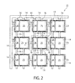
- FIG. 1 is a sectional view of a lead frame according to a first embodiment of the present invention, the sectional view being taken along line I-I in FIG. 2 ;
- FIG. 2 is a plan view showing the lead frame according to the first embodiment of the present invention.
- FIG. 3 is a sectional view of the resin-attached lead frame according to the first embodiment of the present invention, the sectional view being taken along line in FIG. 4 ;
- FIG. 4 is a plan view showing the resin-attached lead frame according to the first embodiment of the present invention.
- FIG. 5 is a sectional view of a semiconductor device relating to the first embodiment of the present invention, the sectional view being taken along line V-V in FIG. 6 ;
- FIG. 6 is a plan view of the semiconductor device relating to the first embodiment of the present invention.
- FIG. 7( a ) to ( g ) shows steps for manufacturing the lead frame according to the first embodiment of the present invention
- FIG. 8( a ) to ( c ) shows further steps for manufacturing the resin-attached lead frame according to the first embodiment of the present invention
- FIG. 9( a ) to ( f ) shows steps for manufacturing the semiconductor device according to the first embodiment of the present invention
- FIG. 10 is a sectional view showing the semiconductor device disposed on an electrical interconnection substrate
- FIG. 11 is a sectional view of a resin-attached lead frame according to a second embodiment of the present invention, the sectional view being taken along line XI-XI in FIG. 12 ;
- FIG. 12 is a plan view showing the resin-attached lead frame according to the second embodiment of the present invention.
- FIG. 13 is a sectional view of a semiconductor device relating to the second embodiment of the present invention, the sectional view being taken along line XIII-XIII in FIG. 14 ;
- FIG. 14 is a plan view of the semiconductor device relating to the second embodiment of the present invention.
- FIG. 15( a ) to ( f ) shows steps for manufacturing the lead frame according to the second embodiment of the present invention
- FIG. 16( a ) to ( d ) shows further steps for manufacturing the resin-attached lead frame according to the second embodiment of the present invention
- FIG. 17 is a sectional view showing a modification of the resin-attached lead frame according to the second embodiment of the present invention.
- FIG. 18 is a sectional view showing another modification of the resin-attached lead frame according to the second embodiment of the present invention.
- FIG. 19 is a sectional view showing yet another modification of the resin-attached lead frame according to the second embodiment of the present invention.
- FIG. 20 is a sectional view showing a further modification of the resin-attached lead frame according to the second embodiment of the present invention.
- FIGS. 1 to 10 a first embodiment of the present invention will be described referring to FIGS. 1 to 10 .
- FIGS. 1 and 2 are a cross-sectional view, and a plan view, respectively, of the lead frame according to the present embodiment.
- the lead frame 15 shown in FIGS. 1 and 2 includes a lead frame main body 11 having a plurality of LED element resting regions 14 , and metallic layers 12 provided on upper surfaces of the LED element resting regions 14 of the lead frame main body 11 , the metallic layers 12 each functioning as a reflecting layer for reflecting light emitted from an LED element 21 .
- the lead frame main body (hereinafter referred to simply as the lead frame body) 11 is formed from a sheet of metal.
- the metal sheet constituting the lead frame body 11 can be of a material such as copper, copper alloy, or 42-alloy (a Fe alloy with a 42% Ni content). Thickness of the lead frame body 11 depends on a configuration of a semiconductor device. Preferable thickness, however, ranges between 0.1 mm and 0.5 mm, inclusive.
- the lead frame body 11 has an outer frame 13 , and the plurality of LED element resting regions 14 are arranged lengthwise and breadthwise inside the outer frame 13 .
- the lead frame body 11 further includes a plurality of die pads (LED element resting portions) 25 and a plurality of lead portions 26 each spaced from one of the die pads 25 , and each LED element resting region 14 is formed over upper surfaces of one die pad 25 and one lead portion 26 .
- a space 17 to be filled in with the reflecting resin section 23 is formed between the die pad 25 and the lead portion 26 .
- the die pad 25 and the lead portion 26 are coupled to another adjacent die pad 25 and another adjacent lead portion 26 , respectively, or to the outer frame 13 , via an independent, rod-shaped tie bar 16 .
- a first outer lead portion 27 is formed on a lower surface of the die pad 25
- a second outer lead portion 28 is formed on a lower surface of the lead section 26 .
- a silver-plated layer 29 is provided on each of the first outer lead portion 27 and the second outer lead portion 28 to enhance a degree of contact with solder.
- the plated layer 29 is preferably 2 ⁇ m to 10 ⁇ m thick.
- Each metallic layer 12 may be formed by, for example, vapor deposition or sputtering, and examples of a material constituting the metallic layer can be aluminum, silver, rhodium, palladium, platinum, copper, and the like.
- a material constituting the metallic layer can be aluminum, silver, rhodium, palladium, platinum, copper, and the like.
- An example in which the metallic layer 12 is formed from a vapor-deposited aluminum layer or a sputtered aluminum layer is described below (hereinafter, this metallic layer is also referred to simply as the vapor-deposited aluminum layer or sputtered aluminum layer 12 ).
- the vapor-deposited aluminum layer or sputtered aluminum layer 12 functioning as a layer for reflecting the light from the LED element 21 , is positioned on the uppermost surface side of the lead frame 15 .
- the vapor-deposited aluminum layer or sputtered aluminum layer 12 is formed by vacuum-vapor-depositing aluminum or sputtering aluminum.
- the vapor-deposited aluminum layer or sputtered aluminum layer 12 is formed to have an extremely small thickness. More specifically, the thickness preferably ranges between 0.1 ⁇ m and 1.0 ⁇ m, inclusive.
- the vapor-deposited aluminum layer or sputtered aluminum layer 12 may be formed directly on the lead frame body 11 , but may be formed thereupon via a bonding layer formed from, for example, a layer plated with silver (Ag).
- the vapor-deposited aluminum layer or sputtered aluminum layer 12 in the present embodiment is provided on an entire upper surface of the lead frame body 11 that includes the outer frame 13 and the tie bars 16 , the vapor-deposited aluminum layer or sputtered aluminum layer 12 needs only to be formed at least in the LED element resting regions 14 on the upper surface of the lead frame body 11 . This is because the LED element resting regions 14 , not shrouded by the reflecting resin section 23 (described later herein) of the lead frame body 11 , are sections that contribute to reflecting the light from each LED element 21 .
- the vapor-deposited aluminum layer or sputtered aluminum layer 12 may be absent on a section of the lead frame body surface that is subjected to wire bonding.
- the vapor-deposited aluminum layer or sputtered aluminum layer 12 may be absent on a section of the lead frame body surface that is subjected to the mounting of an LED element 21 .
- the vapor-deposited aluminum layer or sputtered aluminum layer 12 may be provided on the upper surface of the lead frame body 11 via a bonding layer (not shown) formed from a silver-plated layer, the vapor-deposited aluminum layer or sputtered aluminum layer 12 may not be provided on a section of the lead frame body surface that is subjected to wire bonding.
- the vapor-deposited aluminum layer or sputtered aluminum layer 12 may be provided on the upper surface of the lead frame body 11 via a bonding layer (not shown) formed from a silver-plated layer, the vapor-deposited aluminum layer or sputtered aluminum layer 12 may not be provided on a section of the lead frame body surface that is subjected to the mounting of an LED element 21 .
- each LED element resting region 14 are preferably preworked into a mirror-like finish before the vapor-deposited aluminum layer or sputtered aluminum layer 12 is provided on the upper surfaces.
- Preferable surface roughness of the LED element resting region 14 in this case is such that surface roughness of the LED element resting region 14 as measured using the Optical Surface & Layer Profiling System VertScan 2.0 (manufacturer: Ryoka Systems Inc.) will range between 0.01 ⁇ m and 0.10 ⁇ m, inclusive, in arithmetic average height “Sa” and between 2 ⁇ m and 18 ⁇ m, inclusive, in roughness curvilinear element average length “Sm”. This will increase a reflectance of the vapor-deposited aluminum layer or sputtered aluminum layer 12 formed on the upper surface of the LED element resting region 14 , and thereby achieve more efficient reflection of the light from the LED element 21 .
- grooves 18 for enhancing adhesion between the lead frame body 11 and the reflecting resin section 23 are formed on the upper surface of the lead frame body 11 .
- the grooves 18 each having a rectangular shape in a plane view (except at the space 17 ), are provided along an outer edge of the LED element resting region 14 on the upper surface of the lead frame body 11 .
- Reference symbol S double-dotted chain line in FIG. 2 denotes a region of the lead frame 15 that corresponds to the semiconductor device 20 (see FIGS. 5 and 6 ) detailed later herein.
- the lead frame body 11 includes a plurality of die pads 25 and a plurality of lead portions 26 spaced from one of the die pads 25 , the lead frame body 11 is not limited to this configuration and needs only to include at least one die pad 25 and one lead portion 26 .
- FIGS. 3 and 4 are a cross-sectional view, and a plan view, respectively, of the resin-attached lead frame according to the present embodiment.
- the same elements as those shown in FIGS. 1 and 2 are each assigned the same reference number or symbol.
- the resin-attached lead frame 10 shown in FIGS. 3 and 4 is used to rest LED elements 21 (see FIGS. 5 and 6 ).
- the resin-attached lead frame 10 includes a lead frame 15 and a reflecting resin section 23 provided on the lead frame 15 and surrounding LED element resting regions 14 .
- the lead frame 15 includes a lead frame body 11 , and the lead frame body 11 includes a plurality of die pads 25 and a plurality of lead portions 26 each spaced from one of the die pads 25 .
- An LED element resting region 14 is formed over upper surfaces of each die pad 25 and each lead portion 26 .
- the lead frame body 11 also has a vapor-deposited aluminum layer or sputtered aluminum layer 12 on upper surfaces of each LED element resting region 14 . In FIG. 4 , the vapor-deposited aluminum layer or sputtered aluminum layer 12 is shown in hatched form.
- the lead frame 15 is substantially of the same configuration as that shown in FIGS. 1 and 2 , and detailed description of the lead frame configuration is therefore omitted herein.
- the reflecting resin section 23 is integrated with the lead frame 15 and has a recess 23 a having a substantially rectangular shape in a plane view and surrounding the LED element 21 . Inner walls 23 b are formed on the inside of the recess 23 a . A space 17 filled in with the reflecting resin section 23 also exists between each die pad 25 and each lead portion 26 . Details of the reflecting resin section 23 are described later herein.
- the lead frame body 11 includes a plurality of die pads 25 and a plurality of lead portions 26 spaced from the corresponding die pad 25 , the lead frame body 11 is not limited to this configuration and needs only to include at least one die pad 25 and one lead portion 26 .
- FIGS. 5 and 6 are a cross-sectional view, and a plan view, respectively, of the semiconductor device (SON type) according to the present embodiment.
- the same elements as those shown in FIGS. 1 to 4 are each assigned the same reference number or symbol.
- the semiconductor device 20 includes a (singulated) lead frame 15 having a lead frame body 11 and a vapor-deposited aluminum layer or sputtered aluminum layer 12 , an LED element 21 rested on a die pad 25 of the lead frame 15 , and a bonding wire (electric conductor) 22 that electrically interconnects the LED element 21 and a lead portion 26 of the lead frame 15 .
- the vapor-deposited aluminum layer or sputtered aluminum layer 12 is shown in hatched form in FIG. 6 .
- a reflecting resin section 23 with a recess 23 a is provided around the LED element 21 .
- the LED element 21 and the bonding wire 22 are integrally sealed with a light-transmissive sealing resin 24 .
- the recess 23 a in the reflecting resin section 23 is filled with the sealing resin 24 .
- a region in which the sealing resin 24 is provided corresponds to the LED element resting region 14 .
- the lead frame 15 includes the lead frame body 11 having, as described above, the die pad 25 and the lead portion 26 , and the vapor-deposited aluminum layer or sputtered aluminum layer 12 provided on the lead frame body 11 and functioning as a layer for reflecting light emitted from the LED element 21 .
- a material formed from compound semiconductor single crystals such as GaP, GaAs, GaAlAs, GaAsP, AlInGaP, and/or InGaN, is appropriately selected for a light-emitting layer, a light-emission wavelength ranging between those of ultraviolet light and those of infrared light, inclusive, can be selected for the LED element 21 .
- a commonly used conventional element can be used as such an LED element 21 .
- the LED element 21 is fixedly mounted on the die pad 25 (vapor-deposited aluminum layer or sputtered aluminum layer 12 ), inside the recess 23 a of the reflecting resin section 23 , via solder or a die-bonding paste. If a die-bonding paste is to be used, the die-bonding paste can be that formed from a light-resistant epoxy resin or silicone resin.
- the bonding wire 22 is formed from a highly electroconductive material such as gold, with one end thereof being connected to a terminal section 21 a of the LED element 21 , and with the other end thereof being connected to an upper surface (on the vapor-deposited aluminum layer or sputtered aluminum layer 12 ) of the lead portion 26 .
- the reflecting resin section 23 is formed by, for example, injection-molding a thermoplastic resin over the resin-attached lead frame 10 or by, for example, injection-molding or transfer-molding a thermosetting resin over the resin-attached lead frame 10 .
- the reflecting resin section 23 can vary in shape according to a design of a mold used during the injection molding or transfer molding of the resin.
- the entire reflecting resin section 23 can be formed into a regularly parallelepipedic shape as shown in FIGS. 5 and 6 , or formed into a shape of a cylinder, pyramid/cone, or the like.
- the recess 23 a can have, for example, either a rectangular, circular, elliptical, or polygonal base.
- the inner walls 23 b of the recess 23 a may have either a rectilinear cross-sectional shape as shown in FIG. 5 , or have a curvilinear one.
- thermoplastic resin or thermosetting resin used in the reflecting resin section 23 A material excelling particularly in heat resistance, weatherability, and mechanical strength is desirably selected for the thermoplastic resin or thermosetting resin used in the reflecting resin section 23 .
- the useable kinds of thermoplastic resin materials are polyamide, polyphthalamide (PPA), polyphenylene sulfide, liquid-crystal polymers, polyether sulphone, polyetherimide, polybutylene terephthalate, polyolefin, cyclopolyolefin, and the like.
- thermosetting resin materials are silicone, epoxies, polyimides, and the like.
- a material high in an index of refraction as well as in light transmittance at a light-emission wavelength of the semiconductor device 20 is desirably selected as the sealing resin 24 .
- An epoxy resin or a silicone resin can therefore be selected as a resin that satisfies high heat resistance, weatherability, and mechanical strength requirements.
- the sealing resin 24 is preferably formed from a highly weatherable silicone resin material since the sealing resin 24 is exposed to strong light.
- FIGS. 7( a ) to ( g ) and 8( a ) to ( c ) are described below using FIGS. 7( a ) to ( g ) and 8( a ) to ( c ) .
- a metallic substrate 31 of a flat-plate shape is provided.
- the metallic substrate 31 can be that formed from copper, a copper alloy, a 42-alloy (a Fe alloy with a 42% Ni content), and/or the like. Both sides of the metallic substrate 31 are preferably degreased and cleaned beforehand.
- the metallic substrate 31 preferably has its upper surface 31 a preworked into a mirror-like finish to have a roughness level of 0.01 ⁇ m to 0.1 ⁇ m in arithmetic average height “Sa” and 2 ⁇ m to 18 ⁇ m in roughness curvilinear element average length “Sm”.
- Examples of such mirror-like finishing methods can be by using a mirror-like finishing roller during final rolling of the material, or by conducting double-side mirror-like copper plating.
- photosensitive resists 32 a and 33 a are coated with photosensitive resists 32 a and 33 a , respectively, and then the resists are dried.
- the photosensitive resists 32 a , 33 a can be conventionally known ones.
- Etching resist layers 32 and 33 with desired openings 32 b and 33 b , respectively, are then formed as shown in FIG. 7( c ) .
- etching of the metallic substrate 31 with an etchant occurs using the etching resist layers 32 , 33 as anti-etching films.
- An appropriate chemical as the etchant can be selected according to the kind of metallic substrate material to be used. For example, to use copper as the material of the metallic substrate 31 , the substrate can usually be spray-etched from both sides using an aqueous ferric chloride solution.
- the etching resist layers 32 , 33 are peeled off, whereby the lead frame body 11 with die pads 25 and lead portions 26 spaced from the die pads 25 will then be obtained as shown in FIG. 7( e ) . Providing half etching at this time will also form grooves 18 on the upper surface of the lead frame body 11 .
- the lower surface of the lead frame body 11 is provided with electrolytic plating to deposit a metal (silver) onto a first outer lead portion 27 and a second outer lead portion 28 , thus forming a plated layer 29 for enhanced contact with the solder.
- a metal silver
- FIG. 7( f ) the lead frame body 11 goes through steps such as electrolytic degreasing, pickling, chemical polishing, copper striking, water washing, neutral degreasing, cyanide cleaning, and silver plating, in that order.
- An electroplating solution used in the silver-plating step can be, for example, a silver-plating solution composed mainly of silver cyanide. In an actual process, water washing is added between steps, as required.
- the vapor-deposited aluminum layer or sputtered aluminum layer 12 functioning as a reflecting layer is formed on the entire surface of the lead frame body 11 including the LED element resting region 14 .
- the formation of the vapor-deposited aluminum layer or sputtered aluminum layer is, more specifically, not limited to the above method, but in a case of vapor deposition, the vapor-deposited aluminum layer 12 can be formed on the surface of the lead frame body 11 by using parameters of 9 ⁇ 10 ⁇ 6 torr in maximum attainable degree of vacuum and 1.5 nm/sec in deposition rate. In a case of sputtering, the sputtered aluminum layer 12 can be formed on the surface of the lead frame body 11 by using parameters of 4 ⁇ 10 ⁇ 6 torr in maximum attainable degree of vacuum, 5 ⁇ 10 ⁇ 3 torr in film-forming degree of vacuum, and 900 W in sputtering power (for a target size of 5 inches by 18 inches).
- the reflecting resin section 23 is formed on the vapor-deposited aluminum layer or sputtered aluminum layer 12 of the lead frame 15 .
- the formation of the reflecting resin section 23 is described in further detail below.
- the lead frame 15 that has been obtained through the steps shown in FIG. 7( a ) to ( g ) is mounted in a mold 35 of an injection molding machine or transfer molding machine (not shown). Cavities 35 a appropriate for a shape of the reflecting resin section 23 are preformed in the mold 35 .
- thermosetting resin is poured from a resin supply section (not shown) of the injection molding machine or transfer molding machine into the mold 35 and then allowed to set.
- the reflecting resin section 23 is then formed in a section of the lead frame surface, exclusive of the LED element resting region 14 , as shown in FIG. 8( b ) .
- the reflecting resin section 23 is also generated in the space 17 between the die pad 25 and the lead portion 26 .
- the lead frame 15 with the formed reflecting resin section 23 is removed from the mold 35 after that. In this way, the resin-attached lead frame 10 (see FIGS. 3 and 4 ) with the reflecting resin section 23 and the lead frame 15 is obtained. This state is shown in FIG. 8( c ) .
- FIGS. 5 and 6 Next, a method of manufacturing the semiconductor device 20 shown in FIGS. 5 and 6 is described below using FIG. 9( a ) to ( f ) .
- FIG. 9( a ) shows the fabricated lead frame 10 .
- an LED element 21 is mounted on the die pad 25 of the lead frame 15 .
- the LED element 21 is rested on and fixed to the die pad 25 (the vapor-deposited aluminum layer or sputtered aluminum layer 12 ) of the lead frame 15 by use of solder or a die-bonding paste (this step is called die attaching).
- the terminal section 21 a of the LED element 21 and an upper surface of the lead portion 26 are electrically connected to each other via a bonding wire 22 (this step is called wire bonding).
- the recess 23 a in the reflecting resin 23 is filled in with a sealing resin 24 , whereby the LED element 21 and the bonding wire 22 are sealed with the sealing resin 24 .
- This state is shown in FIG. 9( d ) .
- the lead frame 15 is separated for each LED element 21 by dicing the sections of the lead frame 15 that correspond to the reflecting resin section 23 between the LED elements 21 .
- the lead frame 15 is first rested on and fixed to a dicing tape 37 , and then the reflecting resin section 23 between the LED elements 21 is cut in a vertical direction using, for example, a blade 38 made of a diamond grinding wheel or the like.
- FIG. 9( f ) shows the semiconductor device 20 existing after the reflecting resin section 23 has been cut.
- FIG. 10 is a sectional view showing the semiconductor device disposed on an electrical interconnection substrate.
- the semiconductor device 20 is disposed on the interconnection substrate 41 .
- the interconnection substrate 41 includes a substrate body 42 and interconnection terminal sections 43 and 44 formed on the substrate body 42 .
- the terminal section 43 of the two interconnection terminal sections is connected to a first outer lead portion 27 via a connecting solder portion 45 .
- the other terminal section 44 is connected to a second outer lead portion 28 via a connecting solder portion 46 .
- the semiconductor device 20 is disposed on the interconnection substrate 41 .
- the current is further applied to the LED element 21 on the die pad 25 , thus activating the LED element 21 .
- light from the LED element 21 passes through the sealing resin 24 and is released from an upper surface of the sealing resin 24 , or reflects from the inner walls 23 b of the recess 23 a in the reflecting resin section 23 and is released from the surface of the sealing resin 24 .
- the light from the LED element 21 reflects from the surface of the vapor-deposited aluminum layer or sputtered aluminum layer 12 and is released from the surface of the sealing resin 24 .
- the vapor-deposited aluminum layer or sputtered aluminum layer 12 is provided on the surface of the LED element resting region 14 of the lead frame body 11 .
- the above prevents the lead frame 15 from degrading with time, since the aluminum constituting the vapor-deposited aluminum layer or sputtered aluminum layer 12 is free from degradation due to presence of hydrogen sulfide in air.
- the vapor-deposited aluminum layer or sputtered aluminum layer 12 is provided on the surface of each LED element resting region 14 of the lead frame body 11 . This makes the light from the LED element 21 reflect efficiently and hence enhances the extraction efficiency of the light from the LED element 21 . In addition, the above prevents the lead frame 15 from degrading with time.
- the provision of the vapor-deposited aluminum layer or sputtered aluminum layer 12 in the present embodiment raises adhesion between the lead frame 15 and the sealing resin 24 .
- the state of wire bonding with the bonding wire 22 and the die attaching of the LED elements 21 are also maintained at an appropriate level.
- the vapor-deposited aluminum layer or sputtered aluminum layer 12 is provided via a bonding layer formed from a silver-plated layer, since on the section subjected to wire bonding, the underlying silver (the silver-plated layer) will break the thin aluminum and form an alloy of the silver and the wire, a further desirable bond will be obtained and stronger wire bonding attained.
- the vapor-deposited aluminum layer or sputtered aluminum layer 12 is not provided on the section subjected to wire bonding, since energy for the silver to break an oxide film of the aluminum during wire bonding is not needed, a bonding temperature, parameters relating to use of ultrasonic waves, and other parameters can be alleviated.
- the vapor-deposited aluminum layer or sputtered aluminum layer 12 is provided via a bonding layer formed from a silver-plated layer and not provided on the section subjected to wire bonding, since, the surface of the silver-plated layer can be directly wire-bonded as in conventional technology, a bond with a bonding wire 22 of gold, for example, can be maintained at a high strength level.
- the vapor-deposited aluminum layer or sputtered aluminum layer 12 is provided via a bonding layer formed from a silver-plated layer and not provided on the section where the LED element 21 is to be mounted, when the LED element 21 is to be connected by soldering, for example, high wettability of the solder on that section generates no void in the solder and allows reliable mounting of the entire LED element surface.
- FIGS. 11 to 16 show the second embodiment of the present invention.
- the second embodiment shown in FIGS. 11 to 16 differs from the first embodiment in that a vapor-deposited aluminum layer or sputtered aluminum layer 12 is also provided on inner walls 23 b of a reflecting resin section 23 , and all other elements are substantially the same as those in the first embodiment.
- the same elements as those of the embodiment shown in FIGS. 1 to 10 are each assigned the same reference number or symbol, and detailed description of these elements is omitted herein.
- FIGS. 11 and 12 are a cross-sectional view, and a plan view, respectively, of the resin-attached lead frame according to the present embodiment.
- the resin-attached lead frame 10 A includes a lead frame 15 and a reflecting resin section 23 .
- the lead frame 15 includes a lead frame body 11 , and the lead frame body 11 includes a plurality of die pads 25 and a plurality of lead portions 26 each spaced from one of the die pads 25 .
- An LED element resting region 14 is formed over upper surfaces of each die pad 25 and each lead portion 26 .
- the reflecting resin section 23 is provided in such a form as to surround each of the LED element resting regions 14 of the lead frame body 11 .
- a metallic layer in this case, a vapor-deposited aluminum layer or sputtered aluminum layer 12 is provided on upper surfaces of each LED element resting region 14 of the lead frame body 11 .
- the metallic layer 12 is also provided on the inner walls 23 b of the reflecting resin section 23 . That is to say, the vapor-deposited aluminum layer or sputtered aluminum layer 12 continuously extends along the inner walls 23 b of the reflecting resin section 23 from the surface of the LED element resting region 14 .
- the vapor-deposited aluminum layer or sputtered aluminum layer 12 is shown in hatched form in FIG. 12 .
- the metallic layer 12 formed on the inner walls 23 b of the reflecting resin section 23 as well as on the surface of the LED element resting region 14 is not limited to a vapor-deposited aluminum layer or sputtered aluminum layer and may include layers of silver, rhodium, palladium, platinum, copper, and/or the like.
- the vapor-deposited aluminum layer or sputtered aluminum layer 12 unlike that of the resin-attached lead frame 10 shown in FIGS. 3 and 4 , is not provided between the lead frame body 11 and the reflecting resin section 23 . Instead, the vapor-deposited aluminum layer or sputtered aluminum layer 12 is provided only in each LED element resting region 14 on the surface of the lead frame body 11 .
- the vapor-deposited aluminum layer or sputtered aluminum layer 12 is not provided on a section adjacent to a space 17 , on the inner walls 23 b of the reflecting resin section 23 .
- the resin-attached lead frame 10 A is substantially of the same configuration as that of the resin-attached lead frame 10 shown in FIGS. 3 and 4 , and detailed description of the lead frame configuration is therefore omitted herein.
- the lead frame body 11 includes the die pads 25 and the lead portions 26 spaced from the die pads 25 , the lead frame body 11 is not limited to this configuration and needs only to include at least one die pad 25 and one lead portion 26 .
- FIG. 17 shows a resin-attached lead frame 10 A according to a modification of the present embodiment.
- a reflecting metallic layer 51 is provided on an upper surface 23 C of the reflecting resin section 23 .
- the reflecting metallic layer 51 may be formed from a vapor-deposited aluminum layer or sputtered aluminum layer 12 or formed from other such kinds of metallic layers as of silver, rhodium, palladium, platinum, and/or copper.
- a semiconductor device 20 is built into an illumination device, part of the light emitted from the LED element 21 will commonly or may reflect from the illumination device and return to an upper section of the semiconductor device 20 .
- Providing the reflecting metallic layer 51 as described above prevents the light from being absorbed into the semiconductor device 20 after the light has returned to the upper section thereof.
- FIG. 18 shows a resin-attached lead frame 10 A according to another modification of the present embodiment.
- the resin-attached lead frame 10 A shown, in FIG. 18 differs from that of the modification shown in FIG. 17 , in that a reflecting metallic layer 51 is not provided at a region 23 d on an upper surface 23 c of a reflecting resin section 23 , the region 23 d being a section that will be later cut by dicing as shown in FIG. 9( e ) and where the reflecting resin section 23 is exposed.
- the reflecting metallic layer 51 is provided at all other regions on the upper surface 23 c of the reflecting resin section 23 .
- the section 23 d at which the reflecting resin section 23 is exposed may exist nearly on a central section of the upper surface 23 c of the reflecting resin section 23 or on a position shifted in a horizontal direction from the central section of the upper surface 23 c .
- no foreign substances such as dicing swarf or metallic particles of the highly electroconductive aluminum or other materials will be included, which will in turn prevent short-circuiting due to any metallic foreign substances left after cutting.
- FIG. 19 shows a resin-attached lead frame 10 A according to yet another modification.
- the resin-attached lead frame 10 A shown in FIG. 19 unlike that of the modification shown in FIG. 17 , has a recess 52 concaved inward nearly in a central portion of an upper surface 23 c of a reflecting resin section 23 .
- a reflecting metallic layer 51 is provided in an entire internal region of the recess 52 (including a base 52 a ) in FIG. 19 . Since a reflecting metallic layer 51 does not commonly exist in a section that has been cut by dicing, this section has a property of absorbing light.
- part of the light emitted from the LED element 21 will commonly or may reflect from the illumination device and return to an upper section of the semiconductor device 20 . Since the region that absorbs the light (i.e., the section cut by dicing) is formed to have a small shape and size in FIG. 19 , this geometry prevents the light from being absorbed into the semiconductor device 20 after the light has returned to the upper section thereof.
- FIG. 20 shows a resin-attached lead frame 10 A according to a further modification.
- the resin-attached lead frame 10 A shown in FIG. 20 differs from that of the modification shown in FIG. 19 , in that a reflecting metallic layer 51 is not provided at a base 52 a of a recess 52 , the base 52 a being a section that will be later cut by dicing as shown in FIG. 9( e ) and where a reflecting resin section 23 is exposed.
- the reflecting metallic layer 51 is provided at all other regions of the recess 52 . This configuration prevents light from being absorbed into a semiconductor device 20 after the light has returned to an upper section thereof.
- no foreign substances such as dicing swarf or metallic particles of the highly electroconductive aluminum or other materials will be included, which will in turn prevent short-circuiting due to any metallic foreign substances left after cutting.
- FIG. 13 is a sectional view of the semiconductor device (SON type), and FIG. 14 is a plan view thereof.
- the semiconductor device 20 A includes a (singulated) lead frame 15 having a lead frame body 11 and a vapor-deposited aluminum layer or sputtered aluminum layer 12 , an LED element 21 disposed on a die pad 25 of the lead frame 15 , and a bonding wire (electric conductor) 22 that electrically interconnects the LED element 21 and a lead portion 26 of the lead frame 15 .
- a reflecting resin section 23 is provided around the LED element 21 . Furthermore, the LED element 21 and the bonding wire 22 are both sealed with a light-transmissive sealing resin 24 .
- the vapor-deposited aluminum layer or sputtered aluminum layer 12 is further provided on inner walls 23 b of the reflecting resin section 23 .
- the vapor-deposited aluminum layer or sputtered aluminum layer 12 is shown in hatched form in FIG. 14 .
- the semiconductor device 20 A shown in FIGS. 13 and 14 has substantially the same configuration as that of the semiconductor device 20 shown in FIGS. 5 and 6 , and detailed description of the semiconductor device configuration is omitted herein.
- FIGS. 15( a ) to ( f ) and 16( a ) to ( d ) The following description focuses mainly upon differences with respect to the steps shown in FIGS. 7( a ) to ( g ) and 8( a ) to ( c ) .
- a lead frame body 11 having a die pad 25 and a lead portion 26 disposed away from the die pad 25 is fabricated in steps similar to those shown in FIG. 7( a ) to ( e ) .
- a lower surface of the lead frame body 11 is provided with electrolytic plating to form a silver-plated layer 29 on each of a first outer lead portion 27 and a second outer lead portion 28 .
- a lead frame 15 is obtained.
- the lead frame body 11 may alternatively have its entire surface plated with silver.
- a reflecting resin section 23 is formed on the surface of the lead frame body 11 to integrate the lead frame 15 and the reflecting resin section 23 , as shown in FIG. 16( a ) to ( c ) .
- the step of forming the reflecting resin section 23 is substantially the same as the step of FIG. 8( a ) to ( c ) , except that the reflecting resin section 23 is formed before the vapor-deposited aluminum layer or sputtered aluminum layer 12 is formed.
- the LED element resting region 14 of the lead frame body 11 and the inner walls 23 b of the reflecting resin section 23 are provided with aluminum vapor deposition or aluminum sputtering to form a vapor-deposited aluminum layer or sputtered aluminum layer 12 .
- the resin-attached lead frame 10 A shown in FIGS. 11 and 12 is obtained.
- a method in which the semiconductor device 20 A shown in FIGS. 13 and 14 is fabricated using the thus-obtained resin-attached lead frame 10 A is substantially the same as the method shown in FIG. 9( a ) to ( f ) , and detailed description of the fabrication method is omitted herein.
- the present embodiment enhances the extraction efficiency of the light from the LED element 21 and prevents the lead frame 15 from degrading with time.
- the vapor-deposited aluminum layer or sputtered aluminum layer 12 is also provided on the inner walls 23 b of the reflecting resin section 23 .
- the aluminum constituting the vapor-deposited aluminum layer or sputtered aluminum layer 12 does not degrade even when exposed to the ultraviolet radiation emitted from the LED element 21 , such that the reflecting resin section 23 can be prevented from degrading even when exposed to the ultraviolet radiation.
Landscapes
- Engineering & Computer Science (AREA)
- Microelectronics & Electronic Packaging (AREA)
- Computer Hardware Design (AREA)
- Power Engineering (AREA)
- Manufacturing & Machinery (AREA)
- Physics & Mathematics (AREA)
- Condensed Matter Physics & Semiconductors (AREA)
- General Physics & Mathematics (AREA)
- Led Device Packages (AREA)
- Lead Frames For Integrated Circuits (AREA)
Applications Claiming Priority (3)
| Application Number | Priority Date | Filing Date | Title |
|---|---|---|---|
| JP2011-015274 | 2011-01-27 | ||
| JP2011015274 | 2011-01-27 | ||
| PCT/JP2012/051432 WO2012102266A1 (ja) | 2011-01-27 | 2012-01-24 | 樹脂付リードフレームおよびその製造方法、ならびにリードフレーム |
Related Parent Applications (1)
| Application Number | Title | Priority Date | Filing Date |
|---|---|---|---|
| PCT/JP2012/051432 A-371-Of-International WO2012102266A1 (ja) | 2011-01-27 | 2012-01-24 | 樹脂付リードフレームおよびその製造方法、ならびにリードフレーム |
Related Child Applications (1)
| Application Number | Title | Priority Date | Filing Date |
|---|---|---|---|
| US15/246,608 Continuation US9806241B2 (en) | 2011-01-27 | 2016-08-25 | Resin-attached lead frame and semiconductor device |
Publications (2)
| Publication Number | Publication Date |
|---|---|
| US20130307000A1 US20130307000A1 (en) | 2013-11-21 |
| US9461220B2 true US9461220B2 (en) | 2016-10-04 |
Family
ID=46580832
Family Applications (2)
| Application Number | Title | Priority Date | Filing Date |
|---|---|---|---|
| US13/980,980 Active 2032-04-25 US9461220B2 (en) | 2011-01-27 | 2012-01-24 | Resin-attached lead frame, method for manufacturing the same, and lead frame |
| US15/246,608 Expired - Fee Related US9806241B2 (en) | 2011-01-27 | 2016-08-25 | Resin-attached lead frame and semiconductor device |
Family Applications After (1)
| Application Number | Title | Priority Date | Filing Date |
|---|---|---|---|
| US15/246,608 Expired - Fee Related US9806241B2 (en) | 2011-01-27 | 2016-08-25 | Resin-attached lead frame and semiconductor device |
Country Status (6)
| Country | Link |
|---|---|
| US (2) | US9461220B2 (ko) |
| JP (1) | JP5861943B2 (ko) |
| KR (1) | KR101760545B1 (ko) |
| CN (1) | CN103348499B (ko) |
| TW (1) | TW201250964A (ko) |
| WO (1) | WO2012102266A1 (ko) |
Cited By (3)
| Publication number | Priority date | Publication date | Assignee | Title |
|---|---|---|---|---|
| US20150200138A1 (en) * | 2012-06-05 | 2015-07-16 | Osram Opto Semiconductors Gmbh | Method for producing optoelectronic semiconductor components, leadframe assembly and optoelectronic semiconductor component |
| US9853195B2 (en) | 2015-04-17 | 2017-12-26 | Kabushiki Kaisha Toshiba | Semiconductor light-emitting device and method for producing the same |
| US11251334B2 (en) * | 2019-01-28 | 2022-02-15 | Nichia Corporation | Method of manufacturing light emitting devices |
Families Citing this family (44)
| Publication number | Priority date | Publication date | Assignee | Title |
|---|---|---|---|---|
| US8878215B2 (en) * | 2011-06-22 | 2014-11-04 | Lg Innotek Co., Ltd. | Light emitting device module |
| TWI484670B (zh) * | 2012-11-09 | 2015-05-11 | Fusheng Electronics Corp | 發光二極體的支架結構製作方法(四) |
| JP6111627B2 (ja) * | 2012-12-05 | 2017-04-12 | 大日本印刷株式会社 | 光半導体装置用リードフレーム、樹脂付き光半導体装置用リードフレーム、リードフレームの多面付け体、樹脂付きリードフレームの多面付け体、光半導体装置、光半導体装置の多面付け体 |
| JP6111628B2 (ja) * | 2012-12-05 | 2017-04-12 | 大日本印刷株式会社 | 光半導体装置用リードフレーム、樹脂付き光半導体装置用リードフレーム、リードフレームの多面付け体、樹脂付きリードフレームの多面付け体、光半導体装置、光半導体装置の多面付け体 |
| US9748164B2 (en) * | 2013-03-05 | 2017-08-29 | Nichia Corporation | Semiconductor device |
| JP2015056425A (ja) * | 2013-09-10 | 2015-03-23 | 大日本印刷株式会社 | 光半導体装置、光半導体装置用リードフレーム、及びそれらの製造方法 |
| US10242934B1 (en) * | 2014-05-07 | 2019-03-26 | Utac Headquarters Pte Ltd. | Semiconductor package with full plating on contact side surfaces and methods thereof |
| TWI553264B (zh) * | 2014-05-23 | 2016-10-11 | 億光電子工業股份有限公司 | 承載支架及其製造方法以及從該承載支架所製得之發光裝置及其製造方法 |
| US10177292B2 (en) | 2014-05-23 | 2019-01-08 | Everlight Electronics Co., Ltd. | Carrier, carrier leadframe, and light emitting device |
| JP6501461B2 (ja) * | 2014-07-30 | 2019-04-17 | シチズン電子株式会社 | メッキ膜の剥離防止方法、部品集合体および発光装置 |
| JP6493952B2 (ja) * | 2014-08-26 | 2019-04-03 | 大口マテリアル株式会社 | リードフレーム及びその製造方法 |
| JP6387787B2 (ja) * | 2014-10-24 | 2018-09-12 | 日亜化学工業株式会社 | 発光装置、パッケージ及びそれらの製造方法 |
| US9379087B2 (en) * | 2014-11-07 | 2016-06-28 | Texas Instruments Incorporated | Method of making a QFN package |
| JP6362111B2 (ja) * | 2014-12-01 | 2018-07-25 | 大口マテリアル株式会社 | リードフレームの製造方法 |
| JP6270052B2 (ja) * | 2014-12-05 | 2018-01-31 | Shマテリアル株式会社 | リードフレーム及びその製造方法 |
| US9590158B2 (en) | 2014-12-22 | 2017-03-07 | Nichia Corporation | Light emitting device |
| US9859481B2 (en) * | 2014-12-22 | 2018-01-02 | Nichia Corporation | Light emitting device |
| JP6204610B2 (ja) * | 2015-06-18 | 2017-09-27 | 京セラ株式会社 | 電子素子実装用基板および電子装置 |
| JP6337859B2 (ja) * | 2015-09-08 | 2018-06-06 | 日亜化学工業株式会社 | 発光装置 |
| WO2017056321A1 (ja) * | 2015-10-02 | 2017-04-06 | 大日本印刷株式会社 | 樹脂付リードフレームおよびその製造方法、ならびにledパッケージおよびその製造方法 |
| JP2017157684A (ja) * | 2016-03-02 | 2017-09-07 | ローム株式会社 | 発光装置およびその製造方法 |
| JP6623108B2 (ja) * | 2016-03-31 | 2019-12-18 | 古河電気工業株式会社 | リードフレーム材料およびその製造方法 |
| US20170294367A1 (en) * | 2016-04-07 | 2017-10-12 | Microchip Technology Incorporated | Flat No-Leads Package With Improved Contact Pins |
| JP6644978B2 (ja) * | 2016-07-25 | 2020-02-12 | 大口マテリアル株式会社 | 半導体素子搭載用基板及び半導体装置、並びにそれらの製造方法 |
| JP6825780B2 (ja) * | 2016-07-27 | 2021-02-03 | 大口マテリアル株式会社 | 多列型led用配線部材及びその製造方法 |
| JP6530150B2 (ja) * | 2017-02-09 | 2019-06-12 | 株式会社アクアバンク | 飲料殺菌ユニットおよびこれを備えた飲料水供給装置 |
| US10700252B2 (en) * | 2017-04-18 | 2020-06-30 | Bridgelux Chongqing Co., Ltd. | System and method of manufacture for LED packages |
| CN108933185B (zh) * | 2017-05-26 | 2021-01-05 | 黄国益 | 支撑结构、使用其的发光装置以及其加工方法 |
| JP6969181B2 (ja) * | 2017-07-03 | 2021-11-24 | 沖電気工業株式会社 | 光源用反射体、光源及び光源用反射体の製造方法 |
| JP6829665B2 (ja) * | 2017-07-10 | 2021-02-10 | 新光電気工業株式会社 | リードフレーム、半導体装置、及びリードフレームの製造方法 |
| JP7116881B2 (ja) * | 2017-08-31 | 2022-08-12 | 日亜化学工業株式会社 | パッケージの製造方法及び発光装置の製造方法 |
| US10672954B2 (en) * | 2017-09-01 | 2020-06-02 | Lg Innotek Co., Ltd. | Light emitting device package |
| KR102641336B1 (ko) * | 2017-09-05 | 2024-02-28 | 쑤저우 레킨 세미컨덕터 컴퍼니 리미티드 | 반도체 소자 패키지 |
| KR102401826B1 (ko) * | 2017-09-15 | 2022-05-25 | 쑤저우 레킨 세미컨덕터 컴퍼니 리미티드 | 발광소자 패키지 및 이를 포함하는 조명장치 |
| KR102379733B1 (ko) * | 2017-09-15 | 2022-03-28 | 쑤저우 레킨 세미컨덕터 컴퍼니 리미티드 | 발광소자 패키지 |
| KR102359594B1 (ko) * | 2017-09-19 | 2022-02-07 | 엘지디스플레이 주식회사 | 복합 무기 발광 재료, 발광 필름, 이를 포함하는 엘이디 패키지, 발광다이오드 및 발광장치 |
| CN108321283A (zh) * | 2018-04-03 | 2018-07-24 | 江苏鸿利国泽光电科技有限公司 | 一种高光效紫外led的封装支架及其封装方法 |
| JP6819645B2 (ja) | 2018-04-10 | 2021-01-27 | 日亜化学工業株式会社 | 基板及びそれを用いた発光装置の製造方法 |
| JP7174240B2 (ja) * | 2018-11-30 | 2022-11-17 | 日亜化学工業株式会社 | 発光装置の製造方法 |
| CN111724741A (zh) * | 2020-06-09 | 2020-09-29 | 武汉华星光电半导体显示技术有限公司 | 覆晶薄膜及其制备方法 |
| JP2022014288A (ja) * | 2020-07-06 | 2022-01-19 | 日亜化学工業株式会社 | 発光装置及び発光装置の製造方法 |
| TWM606836U (zh) * | 2020-09-18 | 2021-01-21 | 長華科技股份有限公司 | 導線架 |
| US11715678B2 (en) * | 2020-12-31 | 2023-08-01 | Texas Instruments Incorporated | Roughened conductive components |
| CN113113321B (zh) * | 2021-03-26 | 2022-02-11 | 昆山弗莱吉电子科技有限公司 | 半导体高密度引线框架及其制造工艺 |
Citations (23)
| Publication number | Priority date | Publication date | Assignee | Title |
|---|---|---|---|---|
| US4951119A (en) * | 1988-02-08 | 1990-08-21 | Shinko Electric Industries, Co., Ltd. | Lead frame for semiconductor devices |
| US6355946B1 (en) * | 1998-12-16 | 2002-03-12 | Rohm Co., Ltd. | Semiconductor device with reflector |
| JP2004165567A (ja) | 2002-11-15 | 2004-06-10 | Mitsui High Tec Inc | プリモールドパッケージ用リードフレーム及びその製造方法並びにプリモールドパッケージ及びその製造方法 |
| JP2005019688A (ja) | 2003-06-26 | 2005-01-20 | Kyocera Corp | 発光素子収納用パッケージおよび発光装置 |
| JP2005136379A (ja) | 2003-10-08 | 2005-05-26 | Nichia Chem Ind Ltd | 半導体装置 |
| TWI245437B (en) | 2004-11-16 | 2005-12-11 | Lighthouse Technology Co Ltd | Package structure of a surface mount device light emitting diode |
| JP2006156747A (ja) | 2004-11-30 | 2006-06-15 | Ngk Spark Plug Co Ltd | 配線基板 |
| US20060255357A1 (en) * | 2005-05-11 | 2006-11-16 | Sharp Kabushiki Kaisha | Light emitting element mounting frame and light emitting device |
| JP2007294631A (ja) | 2006-04-25 | 2007-11-08 | Matsushita Electric Works Ltd | 樹脂反射鏡及びこれを用いた照明器具 |
| US20080054288A1 (en) * | 2006-07-05 | 2008-03-06 | Tir Technology Lp | Lighting Device Package |
| JP2008172125A (ja) | 2007-01-15 | 2008-07-24 | Citizen Electronics Co Ltd | チップ型led発光装置及びその製造方法 |
| US20080296604A1 (en) * | 2007-05-30 | 2008-12-04 | I-Chiun Precision Industry Co., Ltd. | Light-emitting diode lead frame and manufacture method thereof |
| US20090141498A1 (en) * | 2007-12-03 | 2009-06-04 | Hitachi Cable Precision Co., Ltd. | Lead frame, method of making the same and light receiving/emitting device |
| WO2010026716A1 (ja) | 2008-09-03 | 2010-03-11 | 日亜化学工業株式会社 | 発光装置、樹脂パッケージ、樹脂成形体並びにこれらの製造方法 |
| WO2010029872A1 (ja) * | 2008-09-09 | 2010-03-18 | 昭和電工株式会社 | 発光装置、発光モジュール、表示装置 |
| US20100078669A1 (en) * | 2008-09-29 | 2010-04-01 | Seoul Semiconductor Co., Ltd. | Light emitting device and lead frame for the same |
| US20100133565A1 (en) * | 2008-12-03 | 2010-06-03 | Seoul Semiconductor Co., Ltd. | Lead frame, light emitting diode having the lead frame, and backlight unit having the light emitting diode |
| US20100193816A1 (en) * | 2009-02-04 | 2010-08-05 | Everlight Electronics Co., Ltd. | Light emitting diode package and fabrication method thereof |
| US20100252848A1 (en) * | 2009-04-01 | 2010-10-07 | Chih-Lung Liang | Method for forming an led lens structure and related structure |
| US20100321941A1 (en) * | 2009-06-22 | 2010-12-23 | Takaaki Sakai | Method for manufacturing light emitting apparatus, light emitting apparatus, and mounting base thereof |
| US20120211785A1 (en) * | 2011-02-23 | 2012-08-23 | Avago Technologies Ecbu Ip (Singapore) Pte. Ltd. | High power plastic leaded chip carrier with integrated metal reflector cup and direct heat sink |
| US20130009190A1 (en) * | 2010-04-07 | 2013-01-10 | Yuhichi Memida | Light emitting device and method for manufacturing same |
| US20130221509A1 (en) * | 2010-11-02 | 2013-08-29 | Dai Nippon Printing Co., Ltd. | Lead frame for mounting led elements, lead frame with resin, method for manufacturing semiconductor devices, and lead frame for mounting semiconductor elements |
Family Cites Families (3)
| Publication number | Priority date | Publication date | Assignee | Title |
|---|---|---|---|---|
| JP3940124B2 (ja) * | 2003-01-16 | 2007-07-04 | 松下電器産業株式会社 | 装置 |
| TWM400099U (en) * | 2010-09-27 | 2011-03-11 | Silitek Electronic Guangzhou | Lead frame, package structure and lighting device thereof |
| US8846421B2 (en) * | 2011-03-10 | 2014-09-30 | Mds Co. Ltd. | Method of manufacturing lead frame for light-emitting device package and light-emitting device package |
-
2012
- 2012-01-20 TW TW101102701A patent/TW201250964A/zh unknown
- 2012-01-24 JP JP2012554800A patent/JP5861943B2/ja active Active
- 2012-01-24 WO PCT/JP2012/051432 patent/WO2012102266A1/ja active Application Filing
- 2012-01-24 KR KR1020137016578A patent/KR101760545B1/ko active IP Right Grant
- 2012-01-24 US US13/980,980 patent/US9461220B2/en active Active
- 2012-01-24 CN CN201280005657.6A patent/CN103348499B/zh not_active Expired - Fee Related
-
2016
- 2016-08-25 US US15/246,608 patent/US9806241B2/en not_active Expired - Fee Related
Patent Citations (30)
| Publication number | Priority date | Publication date | Assignee | Title |
|---|---|---|---|---|
| US4951119A (en) * | 1988-02-08 | 1990-08-21 | Shinko Electric Industries, Co., Ltd. | Lead frame for semiconductor devices |
| US6355946B1 (en) * | 1998-12-16 | 2002-03-12 | Rohm Co., Ltd. | Semiconductor device with reflector |
| JP2004165567A (ja) | 2002-11-15 | 2004-06-10 | Mitsui High Tec Inc | プリモールドパッケージ用リードフレーム及びその製造方法並びにプリモールドパッケージ及びその製造方法 |
| JP2005019688A (ja) | 2003-06-26 | 2005-01-20 | Kyocera Corp | 発光素子収納用パッケージおよび発光装置 |
| JP2005136379A (ja) | 2003-10-08 | 2005-05-26 | Nichia Chem Ind Ltd | 半導体装置 |
| TWI245437B (en) | 2004-11-16 | 2005-12-11 | Lighthouse Technology Co Ltd | Package structure of a surface mount device light emitting diode |
| JP2006156747A (ja) | 2004-11-30 | 2006-06-15 | Ngk Spark Plug Co Ltd | 配線基板 |
| US20060255357A1 (en) * | 2005-05-11 | 2006-11-16 | Sharp Kabushiki Kaisha | Light emitting element mounting frame and light emitting device |
| JP2007294631A (ja) | 2006-04-25 | 2007-11-08 | Matsushita Electric Works Ltd | 樹脂反射鏡及びこれを用いた照明器具 |
| US20080054288A1 (en) * | 2006-07-05 | 2008-03-06 | Tir Technology Lp | Lighting Device Package |
| JP2008172125A (ja) | 2007-01-15 | 2008-07-24 | Citizen Electronics Co Ltd | チップ型led発光装置及びその製造方法 |
| US20080185605A1 (en) | 2007-01-15 | 2008-08-07 | Citizen Electronics Co., Ltd. | Light-emitting diode and method for producing it |
| US20080296604A1 (en) * | 2007-05-30 | 2008-12-04 | I-Chiun Precision Industry Co., Ltd. | Light-emitting diode lead frame and manufacture method thereof |
| US20090141498A1 (en) * | 2007-12-03 | 2009-06-04 | Hitachi Cable Precision Co., Ltd. | Lead frame, method of making the same and light receiving/emitting device |
| WO2010026716A1 (ja) | 2008-09-03 | 2010-03-11 | 日亜化学工業株式会社 | 発光装置、樹脂パッケージ、樹脂成形体並びにこれらの製造方法 |
| US20110210354A1 (en) * | 2008-09-03 | 2011-09-01 | Nichia Corporation | Light emitting device, resin package, resin-molded body, and methods for manufacturing light emitting device, resin package and resin-molded body |
| US8530250B2 (en) * | 2008-09-03 | 2013-09-10 | Nichia Corporation | Light emitting device, resin package, resin-molded body, and methods for manufacturing light emitting device, resin package and resin-molded body |
| EP2325901A1 (en) | 2008-09-03 | 2011-05-25 | Nichia Corporation | Light emitting device, resin package, resin-molded body, and methods for manufacturing light emitting device, resin package and resin-molded body |
| WO2010029872A1 (ja) * | 2008-09-09 | 2010-03-18 | 昭和電工株式会社 | 発光装置、発光モジュール、表示装置 |
| US8378369B2 (en) * | 2008-09-09 | 2013-02-19 | Showa Denko K.K. | Light emitting unit, light emitting module, and display device |
| US20120044667A1 (en) * | 2008-09-09 | 2012-02-23 | Showa Denko K.K. | Light emitting unit, light emitting module, and display device |
| US20100078669A1 (en) * | 2008-09-29 | 2010-04-01 | Seoul Semiconductor Co., Ltd. | Light emitting device and lead frame for the same |
| US20100133565A1 (en) * | 2008-12-03 | 2010-06-03 | Seoul Semiconductor Co., Ltd. | Lead frame, light emitting diode having the lead frame, and backlight unit having the light emitting diode |
| US20100193816A1 (en) * | 2009-02-04 | 2010-08-05 | Everlight Electronics Co., Ltd. | Light emitting diode package and fabrication method thereof |
| US20100252848A1 (en) * | 2009-04-01 | 2010-10-07 | Chih-Lung Liang | Method for forming an led lens structure and related structure |
| JP2011003853A (ja) | 2009-06-22 | 2011-01-06 | Stanley Electric Co Ltd | 発光装置の製造方法、発光装置および発光装置搭載用基板 |
| US20100321941A1 (en) * | 2009-06-22 | 2010-12-23 | Takaaki Sakai | Method for manufacturing light emitting apparatus, light emitting apparatus, and mounting base thereof |
| US20130009190A1 (en) * | 2010-04-07 | 2013-01-10 | Yuhichi Memida | Light emitting device and method for manufacturing same |
| US20130221509A1 (en) * | 2010-11-02 | 2013-08-29 | Dai Nippon Printing Co., Ltd. | Lead frame for mounting led elements, lead frame with resin, method for manufacturing semiconductor devices, and lead frame for mounting semiconductor elements |
| US20120211785A1 (en) * | 2011-02-23 | 2012-08-23 | Avago Technologies Ecbu Ip (Singapore) Pte. Ltd. | High power plastic leaded chip carrier with integrated metal reflector cup and direct heat sink |
Non-Patent Citations (5)
| Title |
|---|
| Apr. 17, 2012 International Search Report issued in International Application No. PCT/JP2012/051432 (with translation). |
| Aug. 6, 2015 Office Action issued in Taiwanese Patent Application No. 101102701. |
| International Preliminary Report on Patentability issued in International Application No. PCT/JP2012/051432 on Jul. 30, 2013 (with translation). |
| May 29, 2015 Office Action issued in Chinese Patent Application No. 201280005657.6. |
| Sep. 4, 2015 Office Action issued in Japanese Application No. 2012-554800. |
Cited By (4)
| Publication number | Priority date | Publication date | Assignee | Title |
|---|---|---|---|---|
| US20150200138A1 (en) * | 2012-06-05 | 2015-07-16 | Osram Opto Semiconductors Gmbh | Method for producing optoelectronic semiconductor components, leadframe assembly and optoelectronic semiconductor component |
| US9741616B2 (en) * | 2012-06-05 | 2017-08-22 | Osram Opto Semiconductors Gmbh | Method for producing optoelectronic semiconductor components, leadframe assembly and optoelectronic semiconductor component |
| US9853195B2 (en) | 2015-04-17 | 2017-12-26 | Kabushiki Kaisha Toshiba | Semiconductor light-emitting device and method for producing the same |
| US11251334B2 (en) * | 2019-01-28 | 2022-02-15 | Nichia Corporation | Method of manufacturing light emitting devices |
Also Published As
| Publication number | Publication date |
|---|---|
| US20130307000A1 (en) | 2013-11-21 |
| US9806241B2 (en) | 2017-10-31 |
| TW201250964A (en) | 2012-12-16 |
| CN103348499B (zh) | 2016-08-10 |
| WO2012102266A1 (ja) | 2012-08-02 |
| KR101760545B1 (ko) | 2017-07-21 |
| JP5861943B2 (ja) | 2016-02-16 |
| KR20130140097A (ko) | 2013-12-23 |
| CN103348499A (zh) | 2013-10-09 |
| US20160365495A1 (en) | 2016-12-15 |
| JPWO2012102266A1 (ja) | 2014-06-30 |
Similar Documents
| Publication | Publication Date | Title |
|---|---|---|
| US9806241B2 (en) | Resin-attached lead frame and semiconductor device | |
| US9773960B2 (en) | Lead frame for mounting LED elements, lead frame with resin, method for manufacturing semiconductor devices, and lead frame for mounting semiconductor elements | |
| TWI476962B (zh) | 發光裝置 | |
| JP5573176B2 (ja) | リードフレームおよびその製造方法、ならびに半導体装置およびその製造方法 | |
| US8629549B2 (en) | Carrier body for a semiconductor component, semiconductor component and method for producing a carrier body | |
| JP5922326B2 (ja) | Led用リードフレームまたは基板およびその製造方法、ならびに半導体装置およびその製造方法 | |
| JP2003046139A (ja) | 発光半導体装置 | |
| JP2007194401A (ja) | 化合物半導体発光素子を用いたledパッケージ | |
| TWI739919B (zh) | 發光裝置、發光裝置用封裝及發光裝置之製造方法 | |
| JP5737605B2 (ja) | Led用リードフレームまたは基板およびその製造方法、ならびに半導体装置およびその製造方法 | |
| JP5871174B2 (ja) | Led用リードフレームまたは基板、半導体装置、およびled用リードフレームまたは基板の製造方法 | |
| KR101526087B1 (ko) | 광전 소자용 하우징 및 그 하우징의 제조 방법 | |
| US10249804B2 (en) | Semiconductor device, base, and method for manufacturing same | |
| KR20090103292A (ko) | Led 패키지 | |
| TWI521745B (zh) | 發光二極體封裝結構及其製造方法 | |
| JP5998609B2 (ja) | 光半導体装置 | |
| JP2021012973A (ja) | 半導体発光装置 | |
| KR20170126839A (ko) | 반도체 발광소자 |
Legal Events
| Date | Code | Title | Description |
|---|---|---|---|
| AS | Assignment |
Owner name: DAI NIPPON PRINTING CO., LTD., JAPAN Free format text: ASSIGNMENT OF ASSIGNORS INTEREST;ASSIGNORS:IKENAGA, CHIKAO;ODA, KAZUNORI;REEL/FRAME:030892/0526 Effective date: 20130705 |
|
| STCF | Information on status: patent grant |
Free format text: PATENTED CASE |
|
| FEPP | Fee payment procedure |
Free format text: PAYOR NUMBER ASSIGNED (ORIGINAL EVENT CODE: ASPN); ENTITY STATUS OF PATENT OWNER: LARGE ENTITY |
|
| MAFP | Maintenance fee payment |
Free format text: PAYMENT OF MAINTENANCE FEE, 4TH YEAR, LARGE ENTITY (ORIGINAL EVENT CODE: M1551); ENTITY STATUS OF PATENT OWNER: LARGE ENTITY Year of fee payment: 4 |
|
| MAFP | Maintenance fee payment |
Free format text: PAYMENT OF MAINTENANCE FEE, 8TH YEAR, LARGE ENTITY (ORIGINAL EVENT CODE: M1552); ENTITY STATUS OF PATENT OWNER: LARGE ENTITY Year of fee payment: 8 |