US8497476B2 - Inspection device - Google Patents
Inspection device Download PDFInfo
- Publication number
- US8497476B2 US8497476B2 US13/420,731 US201213420731A US8497476B2 US 8497476 B2 US8497476 B2 US 8497476B2 US 201213420731 A US201213420731 A US 201213420731A US 8497476 B2 US8497476 B2 US 8497476B2
- Authority
- US
- United States
- Prior art keywords
- present
- lens
- electron
- optical system
- electrons
- Prior art date
- Legal status (The legal status is an assumption and is not a legal conclusion. Google has not performed a legal analysis and makes no representation as to the accuracy of the status listed.)
- Active
Links
Images


Classifications
-
- G—PHYSICS
- G01—MEASURING; TESTING
- G01N—INVESTIGATING OR ANALYSING MATERIALS BY DETERMINING THEIR CHEMICAL OR PHYSICAL PROPERTIES
- G01N23/00—Investigating or analysing materials by the use of wave or particle radiation, e.g. X-rays or neutrons, not covered by groups G01N3/00 – G01N17/00, G01N21/00 or G01N22/00
- G01N23/22—Investigating or analysing materials by the use of wave or particle radiation, e.g. X-rays or neutrons, not covered by groups G01N3/00 – G01N17/00, G01N21/00 or G01N22/00 by measuring secondary emission from the material
- G01N23/225—Investigating or analysing materials by the use of wave or particle radiation, e.g. X-rays or neutrons, not covered by groups G01N3/00 – G01N17/00, G01N21/00 or G01N22/00 by measuring secondary emission from the material using electron or ion
- G01N23/2251—Investigating or analysing materials by the use of wave or particle radiation, e.g. X-rays or neutrons, not covered by groups G01N3/00 – G01N17/00, G01N21/00 or G01N22/00 by measuring secondary emission from the material using electron or ion using incident electron beams, e.g. scanning electron microscopy [SEM]
-
- G—PHYSICS
- G01—MEASURING; TESTING
- G01N—INVESTIGATING OR ANALYSING MATERIALS BY DETERMINING THEIR CHEMICAL OR PHYSICAL PROPERTIES
- G01N21/00—Investigating or analysing materials by the use of optical means, i.e. using sub-millimetre waves, infrared, visible or ultraviolet light
- G01N21/84—Systems specially adapted for particular applications
- G01N21/88—Investigating the presence of flaws or contamination
- G01N21/95—Investigating the presence of flaws or contamination characterised by the material or shape of the object to be examined
- G01N21/956—Inspecting patterns on the surface of objects
-
- G—PHYSICS
- G01—MEASURING; TESTING
- G01N—INVESTIGATING OR ANALYSING MATERIALS BY DETERMINING THEIR CHEMICAL OR PHYSICAL PROPERTIES
- G01N23/00—Investigating or analysing materials by the use of wave or particle radiation, e.g. X-rays or neutrons, not covered by groups G01N3/00 – G01N17/00, G01N21/00 or G01N22/00
- G01N23/22—Investigating or analysing materials by the use of wave or particle radiation, e.g. X-rays or neutrons, not covered by groups G01N3/00 – G01N17/00, G01N21/00 or G01N22/00 by measuring secondary emission from the material
- G01N23/223—Investigating or analysing materials by the use of wave or particle radiation, e.g. X-rays or neutrons, not covered by groups G01N3/00 – G01N17/00, G01N21/00 or G01N22/00 by measuring secondary emission from the material by irradiating the sample with X-rays or gamma-rays and by measuring X-ray fluorescence
-
- H—ELECTRICITY
- H01—ELECTRIC ELEMENTS
- H01J—ELECTRIC DISCHARGE TUBES OR DISCHARGE LAMPS
- H01J1/00—Details of electrodes, of magnetic control means, of screens, or of the mounting or spacing thereof, common to two or more basic types of discharge tubes or lamps
- H01J1/02—Main electrodes
- H01J1/34—Photo-emissive cathodes
-
- H—ELECTRICITY
- H01—ELECTRIC ELEMENTS
- H01J—ELECTRIC DISCHARGE TUBES OR DISCHARGE LAMPS
- H01J37/00—Discharge tubes with provision for introducing objects or material to be exposed to the discharge, e.g. for the purpose of examination or processing thereof
- H01J37/02—Details
- H01J37/04—Arrangements of electrodes and associated parts for generating or controlling the discharge, e.g. electron-optical arrangement, ion-optical arrangement
- H01J37/06—Electron sources; Electron guns
- H01J37/073—Electron guns using field emission, photo emission, or secondary emission electron sources
-
- H—ELECTRICITY
- H01—ELECTRIC ELEMENTS
- H01J—ELECTRIC DISCHARGE TUBES OR DISCHARGE LAMPS
- H01J37/00—Discharge tubes with provision for introducing objects or material to be exposed to the discharge, e.g. for the purpose of examination or processing thereof
- H01J37/02—Details
- H01J37/04—Arrangements of electrodes and associated parts for generating or controlling the discharge, e.g. electron-optical arrangement, ion-optical arrangement
- H01J37/09—Diaphragms; Shields associated with electron or ion-optical arrangements; Compensation of disturbing fields
-
- H—ELECTRICITY
- H01—ELECTRIC ELEMENTS
- H01J—ELECTRIC DISCHARGE TUBES OR DISCHARGE LAMPS
- H01J37/00—Discharge tubes with provision for introducing objects or material to be exposed to the discharge, e.g. for the purpose of examination or processing thereof
- H01J37/02—Details
- H01J37/04—Arrangements of electrodes and associated parts for generating or controlling the discharge, e.g. electron-optical arrangement, ion-optical arrangement
- H01J37/10—Lenses
-
- H—ELECTRICITY
- H01—ELECTRIC ELEMENTS
- H01J—ELECTRIC DISCHARGE TUBES OR DISCHARGE LAMPS
- H01J37/00—Discharge tubes with provision for introducing objects or material to be exposed to the discharge, e.g. for the purpose of examination or processing thereof
- H01J37/02—Details
- H01J37/20—Means for supporting or positioning the objects or the material; Means for adjusting diaphragms or lenses associated with the support
-
- H—ELECTRICITY
- H01—ELECTRIC ELEMENTS
- H01J—ELECTRIC DISCHARGE TUBES OR DISCHARGE LAMPS
- H01J37/00—Discharge tubes with provision for introducing objects or material to be exposed to the discharge, e.g. for the purpose of examination or processing thereof
- H01J37/02—Details
- H01J37/22—Optical or photographic arrangements associated with the tube
- H01J37/222—Image processing arrangements associated with the tube
-
- H—ELECTRICITY
- H01—ELECTRIC ELEMENTS
- H01J—ELECTRIC DISCHARGE TUBES OR DISCHARGE LAMPS
- H01J37/00—Discharge tubes with provision for introducing objects or material to be exposed to the discharge, e.g. for the purpose of examination or processing thereof
- H01J37/02—Details
- H01J37/244—Detectors; Associated components or circuits therefor
-
- H—ELECTRICITY
- H01—ELECTRIC ELEMENTS
- H01J—ELECTRIC DISCHARGE TUBES OR DISCHARGE LAMPS
- H01J37/00—Discharge tubes with provision for introducing objects or material to be exposed to the discharge, e.g. for the purpose of examination or processing thereof
- H01J37/26—Electron or ion microscopes; Electron or ion diffraction tubes
- H01J37/261—Details
- H01J37/265—Controlling the tube; circuit arrangements adapted to a particular application not otherwise provided, e.g. bright-field-dark-field illumination
-
- H—ELECTRICITY
- H01—ELECTRIC ELEMENTS
- H01J—ELECTRIC DISCHARGE TUBES OR DISCHARGE LAMPS
- H01J37/00—Discharge tubes with provision for introducing objects or material to be exposed to the discharge, e.g. for the purpose of examination or processing thereof
- H01J37/26—Electron or ion microscopes; Electron or ion diffraction tubes
- H01J37/28—Electron or ion microscopes; Electron or ion diffraction tubes with scanning beams
-
- H—ELECTRICITY
- H01—ELECTRIC ELEMENTS
- H01J—ELECTRIC DISCHARGE TUBES OR DISCHARGE LAMPS
- H01J37/00—Discharge tubes with provision for introducing objects or material to be exposed to the discharge, e.g. for the purpose of examination or processing thereof
- H01J37/26—Electron or ion microscopes; Electron or ion diffraction tubes
- H01J37/29—Reflection microscopes
-
- G—PHYSICS
- G01—MEASURING; TESTING
- G01N—INVESTIGATING OR ANALYSING MATERIALS BY DETERMINING THEIR CHEMICAL OR PHYSICAL PROPERTIES
- G01N2223/00—Investigating materials by wave or particle radiation
- G01N2223/60—Specific applications or type of materials
- G01N2223/611—Specific applications or type of materials patterned objects; electronic devices
-
- H—ELECTRICITY
- H01—ELECTRIC ELEMENTS
- H01J—ELECTRIC DISCHARGE TUBES OR DISCHARGE LAMPS
- H01J2237/00—Discharge tubes exposing object to beam, e.g. for analysis treatment, etching, imaging
- H01J2237/004—Charge control of objects or beams
- H01J2237/0048—Charging arrangements
-
- H—ELECTRICITY
- H01—ELECTRIC ELEMENTS
- H01J—ELECTRIC DISCHARGE TUBES OR DISCHARGE LAMPS
- H01J2237/00—Discharge tubes exposing object to beam, e.g. for analysis treatment, etching, imaging
- H01J2237/02—Details
- H01J2237/022—Avoiding or removing foreign or contaminating particles, debris or deposits on sample or tube
-
- H—ELECTRICITY
- H01—ELECTRIC ELEMENTS
- H01J—ELECTRIC DISCHARGE TUBES OR DISCHARGE LAMPS
- H01J2237/00—Discharge tubes exposing object to beam, e.g. for analysis treatment, etching, imaging
- H01J2237/03—Mounting, supporting, spacing or insulating electrodes
- H01J2237/032—Mounting or supporting
-
- H—ELECTRICITY
- H01—ELECTRIC ELEMENTS
- H01J—ELECTRIC DISCHARGE TUBES OR DISCHARGE LAMPS
- H01J2237/00—Discharge tubes exposing object to beam, e.g. for analysis treatment, etching, imaging
- H01J2237/03—Mounting, supporting, spacing or insulating electrodes
- H01J2237/038—Insulating
-
- H—ELECTRICITY
- H01—ELECTRIC ELEMENTS
- H01J—ELECTRIC DISCHARGE TUBES OR DISCHARGE LAMPS
- H01J2237/00—Discharge tubes exposing object to beam, e.g. for analysis treatment, etching, imaging
- H01J2237/04—Means for controlling the discharge
- H01J2237/045—Diaphragms
-
- H—ELECTRICITY
- H01—ELECTRIC ELEMENTS
- H01J—ELECTRIC DISCHARGE TUBES OR DISCHARGE LAMPS
- H01J2237/00—Discharge tubes exposing object to beam, e.g. for analysis treatment, etching, imaging
- H01J2237/04—Means for controlling the discharge
- H01J2237/045—Diaphragms
- H01J2237/0456—Supports
- H01J2237/0458—Supports movable, i.e. for changing between differently sized apertures
-
- H—ELECTRICITY
- H01—ELECTRIC ELEMENTS
- H01J—ELECTRIC DISCHARGE TUBES OR DISCHARGE LAMPS
- H01J2237/00—Discharge tubes exposing object to beam, e.g. for analysis treatment, etching, imaging
- H01J2237/04—Means for controlling the discharge
- H01J2237/047—Changing particle velocity
- H01J2237/0473—Changing particle velocity accelerating
-
- H—ELECTRICITY
- H01—ELECTRIC ELEMENTS
- H01J—ELECTRIC DISCHARGE TUBES OR DISCHARGE LAMPS
- H01J2237/00—Discharge tubes exposing object to beam, e.g. for analysis treatment, etching, imaging
- H01J2237/04—Means for controlling the discharge
- H01J2237/049—Focusing means
- H01J2237/0492—Lens systems
-
- H—ELECTRICITY
- H01—ELECTRIC ELEMENTS
- H01J—ELECTRIC DISCHARGE TUBES OR DISCHARGE LAMPS
- H01J2237/00—Discharge tubes exposing object to beam, e.g. for analysis treatment, etching, imaging
- H01J2237/06—Sources
- H01J2237/061—Construction
-
- H—ELECTRICITY
- H01—ELECTRIC ELEMENTS
- H01J—ELECTRIC DISCHARGE TUBES OR DISCHARGE LAMPS
- H01J2237/00—Discharge tubes exposing object to beam, e.g. for analysis treatment, etching, imaging
- H01J2237/06—Sources
- H01J2237/063—Electron sources
- H01J2237/06325—Cold-cathode sources
- H01J2237/06333—Photo emission
-
- H—ELECTRICITY
- H01—ELECTRIC ELEMENTS
- H01J—ELECTRIC DISCHARGE TUBES OR DISCHARGE LAMPS
- H01J2237/00—Discharge tubes exposing object to beam, e.g. for analysis treatment, etching, imaging
- H01J2237/16—Vessels
- H01J2237/166—Sealing means
-
- H—ELECTRICITY
- H01—ELECTRIC ELEMENTS
- H01J—ELECTRIC DISCHARGE TUBES OR DISCHARGE LAMPS
- H01J2237/00—Discharge tubes exposing object to beam, e.g. for analysis treatment, etching, imaging
- H01J2237/18—Vacuum control means
- H01J2237/186—Valves
-
- H—ELECTRICITY
- H01—ELECTRIC ELEMENTS
- H01J—ELECTRIC DISCHARGE TUBES OR DISCHARGE LAMPS
- H01J2237/00—Discharge tubes exposing object to beam, e.g. for analysis treatment, etching, imaging
- H01J2237/20—Positioning, supporting, modifying or maintaining the physical state of objects being observed or treated
- H01J2237/2002—Controlling environment of sample
-
- H—ELECTRICITY
- H01—ELECTRIC ELEMENTS
- H01J—ELECTRIC DISCHARGE TUBES OR DISCHARGE LAMPS
- H01J2237/00—Discharge tubes exposing object to beam, e.g. for analysis treatment, etching, imaging
- H01J2237/20—Positioning, supporting, modifying or maintaining the physical state of objects being observed or treated
- H01J2237/2007—Holding mechanisms
-
- H—ELECTRICITY
- H01—ELECTRIC ELEMENTS
- H01J—ELECTRIC DISCHARGE TUBES OR DISCHARGE LAMPS
- H01J2237/00—Discharge tubes exposing object to beam, e.g. for analysis treatment, etching, imaging
- H01J2237/20—Positioning, supporting, modifying or maintaining the physical state of objects being observed or treated
- H01J2237/2008—Positioning, supporting, modifying or maintaining the physical state of objects being observed or treated specially adapted for studying electrical or magnetical properties of objects
-
- H—ELECTRICITY
- H01—ELECTRIC ELEMENTS
- H01J—ELECTRIC DISCHARGE TUBES OR DISCHARGE LAMPS
- H01J2237/00—Discharge tubes exposing object to beam, e.g. for analysis treatment, etching, imaging
- H01J2237/244—Detection characterized by the detecting means
- H01J2237/2448—Secondary particle detectors
-
- H—ELECTRICITY
- H01—ELECTRIC ELEMENTS
- H01J—ELECTRIC DISCHARGE TUBES OR DISCHARGE LAMPS
- H01J2237/00—Discharge tubes exposing object to beam, e.g. for analysis treatment, etching, imaging
- H01J2237/248—Components associated with the control of the tube
- H01J2237/2482—Optical means
-
- H—ELECTRICITY
- H01—ELECTRIC ELEMENTS
- H01J—ELECTRIC DISCHARGE TUBES OR DISCHARGE LAMPS
- H01J2237/00—Discharge tubes exposing object to beam, e.g. for analysis treatment, etching, imaging
- H01J2237/248—Components associated with the control of the tube
- H01J2237/2485—Electric or electronic means
-
- H—ELECTRICITY
- H01—ELECTRIC ELEMENTS
- H01J—ELECTRIC DISCHARGE TUBES OR DISCHARGE LAMPS
- H01J2237/00—Discharge tubes exposing object to beam, e.g. for analysis treatment, etching, imaging
- H01J2237/26—Electron or ion microscopes
- H01J2237/28—Scanning microscopes
- H01J2237/2813—Scanning microscopes characterised by the application
- H01J2237/2817—Pattern inspection
-
- H—ELECTRICITY
- H01—ELECTRIC ELEMENTS
- H01J—ELECTRIC DISCHARGE TUBES OR DISCHARGE LAMPS
- H01J2237/00—Discharge tubes exposing object to beam, e.g. for analysis treatment, etching, imaging
- H01J2237/26—Electron or ion microscopes
- H01J2237/285—Emission microscopes
- H01J2237/2855—Photo-emission
-
- H—ELECTRICITY
- H01—ELECTRIC ELEMENTS
- H01J—ELECTRIC DISCHARGE TUBES OR DISCHARGE LAMPS
- H01J2237/00—Discharge tubes exposing object to beam, e.g. for analysis treatment, etching, imaging
- H01J2237/26—Electron or ion microscopes
- H01J2237/285—Emission microscopes
- H01J2237/2857—Particle bombardment induced emission
Definitions
- the present invention relates to an inspection device and methods for inspecting foreign materials, particles, and/or defects in patterns formed on the surface of an object to be inspected, and more particularly, to an inspection device and inspection method in which secondary electrons which vary in accordance with the properties of the surface are captured thereof to form image data, and inspecting patterns formed on the surface of the object to be inspected based on the image data at a high throughput.
- a sample can be an exposure mask, an EUV mask, a nano print mask (and template) a semiconductor wafer, an optical element substrate, or optical circuit substrate etc. These are separated into those with patterns and those without patterns. Those that include patterns are further separated into those that have uneven structure and those that do not. A pattern that does not include uneven structure is formed using a different material. Those that do not include patterns are separated into those that are coated with an oxide film and those that are not coated with an oxide film.
- the first problem is related to a deficiency in resolution and throughput.
- pixel size was about 50 nm and aberration was about 200 nm. Further, it was necessary to reduce aberration, reduce the energy width of an irradiation current, reduce pixel size and increase the amount of current in order to improve high resolution capabilities and throughput.
- the present invention aims to provide an inspection method and an inspection device which solves the defects of a conventional inspection device described above, can improve inspection accuracy and can be applied to 5 ⁇ 30 nm design rules.
- an inspection device for inspecting a surface of an inspection object using a beam including a beam generator which is capable of generating one of either charge particles or an electromagnetic wave as a beam, a primary optical system which is capable of guiding and irradiating the beam to the inspection object supported within a working chamber, a secondary optical system which is capable of including a first movable numerical aperture and a first detector which detects secondary charge particles generated from the inspection object, the secondary charge particles passing through the first movable numerical aperture, an image processing system which is capable of forming an image based on the secondary charge particles detected by the first detector, and a second detector arranged between the first movable numerical aperture and the first detector and which detects a location and shape at a cross over location of the secondary charge particles generated from the inspection object.
- the first detector may detect the secondary charge particles in a state where the location of the first movable numerical aperture is adjusted based on a detection result of the second detector.
- the beam may be a beam of charged particles
- the beam generator may include a photoelectron element formed by coating a photoelectron material on a planar part of a base material comprised from a transmittance part including the planar part, the photoelectron element receiving light irradiated from the photoelectron material to generate photoelectrons, one or more lenses each arranged at a predetermined intervals after the photoelectron element respectively, the one or more lenses accelerating photoelectrons generated from the photoelectron element, a second numerical aperture arranged on the lower side of the one or more lenses, and a cathode lens arranged after the numerical aperture.
- the beam may be an electromagnetic wave beam
- the beam generator may generate a plurality of beams with different wavelengths.
- the first detector may detect the secondary charge particles generated from a surface of the inspection object irradiated with the beam.
- the first detector may detect the secondary charge particles generated from a surface opposite a surface of the inspection object irradiated with the beam.
- the first detector may include a TDI.
- the second detector may include an EB-CDD.
- the first movable numerical aperture may include an open part formed by a plus shape or slit.
- the inspection device 1 may further include an optical microscope and a SEM (scanning type electron microscope) which observes the inspection object, wherein the beam generator, the primary optical system, the secondary optical system, the image processing system, the optical microscope and the SEM are arranged in the working chamber.
- an optical microscope and a SEM scanning type electron microscope
- the secondary charge particles described above may be a part of or a mixture of secondary emission electrons, mirror electrons and photoelectrons.
- Photoelectrons are generated from a sample surface when an electromagnetic wave is irradiated. Secondary emission electrons are generated when charge particles such an electron beam is irradiated to a sample surface. Alternatively, mirror electrons are formed. Secondary emission electrons are generated when an electron beam collides with a sample surface. That is, secondary emission electrons are a part of or mixture of secondary electrons, reflected electrons and back scattered electrons. In addition, electrons reflected near a surface where an irradiated electron beam does not collide with a sample surface are called mirror electrons.
- FIG. 1 is an elevated view diagram which shows the main structural elements of an inspection device of the present invention related to one embodiment, seen along the line A-A in FIG. 2 ;
- FIG. 2A is a planar view diagram of the main structural elements of the inspection device shown in FIG. 1 , seen along the line B-B in FIG. 1 ;
- FIG. 2B is an approximate cross-sectional diagram which shows another example of a substrate transfer device in the inspection device of the present invention related to one embodiment
- FIG. 3 is a cross-sectional diagram which shows the mini environment in FIG. 1 seen along the line C-C;
- FIG. 4 is a diagram which shows the loader housing in FIG. 1 seen along the line D-D in FIG. 2 ;
- FIG. 5 is an expanded view diagram of a wafer rack, [A] is a side view diagram and [B] is a cross-sectional view diagram seen along the line E-E of [A];
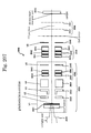
- FIG. 6 is a diagram which shows modifications of a method for supporting a main housing
- FIG. 7 is a diagram which shows modifications of a method for supporting a main housing
- FIG. 8 is a schematic diagram which shows an approximate structure of an electron optical device of the inspection device in FIG. 1 ;
- FIG. 9 is a diagram related to one embodiment of the present invention.
- FIG. 10 is a diagram related to one embodiment of the present invention.
- FIG. 11 is a diagram related to one embodiment of the present invention.
- FIG. 12 is a diagram related to one embodiment of the present invention.
- FIG. 13 is a diagram related to one embodiment of the present invention.
- FIG. 14 is a diagram related to one embodiment of the present invention.
- FIG. 15 is a diagram related to one embodiment of the present invention.
- FIG. 16 is a diagram related to one embodiment of the present invention.
- FIG. 17 is a diagram related to one embodiment of the present invention.
- FIG. 18 is a diagram related to one embodiment of the present invention.
- FIG. 19 is a diagram related to one embodiment of the present invention.
- FIG. 20 is a diagram related to one embodiment of the present invention.
- FIG. 21 is a diagram related to one embodiment of the present invention.
- FIG. 22 is a diagram related to one embodiment of the present invention.
- FIG. 23 is a diagram related to one embodiment of the present invention.
- FIG. 24 is a diagram related to one embodiment of the present invention.
- FIG. 25 is a diagram related to one embodiment of the present invention.
- FIG. 26A is a diagram related to one embodiment of the present invention.
- FIG. 26B is a diagram related to one embodiment of the present invention.
- FIG. 26C is a diagram related to one embodiment of the present invention.
- FIG. 27A is a diagram related to one embodiment of the present invention.
- FIG. 27B is a diagram related to one embodiment of the present invention.
- FIG. 28 is a diagram related to one embodiment of the present invention.
- FIG. 29A is a diagram related to one embodiment of the present invention.
- FIG. 28B is a diagram related to one embodiment of the present invention.
- FIG. 30 is a diagram related to one embodiment of the present invention.
- FIG. 31 is a diagram related to one embodiment of the present invention.
- FIG. 32A is a diagram related to one embodiment of the present invention.
- FIG. 32B is a diagram related to one embodiment of the present invention.
- FIG. 32C is a diagram related to one embodiment of the present invention.
- FIG. 32D is a diagram related to one embodiment of the present invention.
- FIG. 32E is a diagram related to one embodiment of the present invention.
- FIG. 33 is a diagram related to one embodiment of the present invention.
- FIG. 34 is a diagram related to one embodiment of the present invention.
- FIG. 35 is a diagram related to one embodiment of the present invention.
- FIG. 36 is a diagram related to one embodiment of the present invention.
- FIG. 37 is a diagram related to one embodiment of the present invention.
- FIG. 38 is a diagram related to one embodiment of the present invention.
- FIG. 39 is a diagram related to one embodiment of the present invention.
- FIG. 40 is a diagram related to one embodiment of the present invention.
- FIG. 41 is a diagram related to one embodiment of the present invention.
- FIG. 42 is a diagram related to one embodiment of the present invention.
- FIG. 43 is a diagram related to one embodiment of the present invention.
- FIG. 44 is a diagram related to one embodiment of the present invention.
- FIG. 45 is a diagram related to one embodiment of the present invention.
- FIG. 46 is a diagram related to one embodiment of the present invention.
- FIG. 47 is a diagram related to one embodiment of the present invention.
- FIG. 48 is a diagram related to one embodiment of the present invention.
- FIG. 49 is a diagram related to one embodiment of the present invention.
- FIG. 50 is a diagram related to one embodiment of the present invention.
- FIG. 51 is a diagram related to one embodiment of the present invention.
- FIG. 52 is a diagram related to one embodiment of the present invention.
- FIG. 53 is a diagram related to one embodiment of the present invention.
- FIG. 54 is a diagram related to one embodiment of the present invention.
- FIG. 55 is a diagram related to one embodiment of the present invention.
- FIG. 56 is a diagram related to one embodiment of the present invention.
- FIG. 57 is a diagram related to one embodiment of the present invention.
- FIG. 58 is a diagram related to one embodiment of the present invention.
- FIG. 59 is a diagram related to one embodiment of the present invention.
- FIG. 60 is a diagram related to one embodiment of the present invention.
- FIG. 61 is a diagram related to one embodiment of the present invention.
- FIG. 62 is a diagram related to one embodiment of the present invention.
- FIG. 63 is a diagram related to one embodiment of the present invention.
- FIG. 64 is a diagram related to one embodiment of the present invention.
- FIG. 65 is a diagram related to one embodiment of the present invention.
- FIG. 66 is a diagram related to one embodiment of the present invention.
- FIG. 67 is a diagram related to one embodiment of the present invention.
- FIG. 68 is a diagram related to one embodiment of the present invention.
- FIG. 69 is a diagram related to one embodiment of the present invention.
- FIG. 70 is a diagram related to one embodiment of the present invention.
- FIG. 71 is a diagram related to one embodiment of the present invention.
- FIG. 72 is a diagram related to one embodiment of the present invention.
- FIG. 73 is a diagram related to one embodiment of the present invention.
- FIG. 74 is a diagram related to one embodiment of the present invention.
- FIG. 75 is a diagram related to one embodiment of the present invention.
- FIG. 76 is a diagram related to one embodiment of the present invention.
- FIG. 77 is a diagram related to one embodiment of the present invention.
- FIG. 78 is a diagram related to one embodiment of the present invention.
- FIG. 79 is a diagram related to one embodiment of the present invention.
- FIG. 80 is a diagram related to one embodiment of the present invention.
- FIG. 81 is a diagram related to one embodiment of the present invention.
- FIG. 82 is a diagram related to one embodiment of the present invention.
- FIG. 83 is a diagram related to one embodiment of the present invention.
- FIG. 84 is a diagram related to one embodiment of the present invention.
- FIG. 85 is a diagram related to one embodiment of the present invention.
- FIG. 86 is a diagram related to one embodiment of the present invention.
- FIG. 87 is a diagram related to one embodiment of the present invention.
- FIG. 88 is a diagram related to one embodiment of the present invention.
- FIG. 89 is a diagram related to one embodiment of the present invention.
- FIG. 90 is a diagram related to one embodiment of the present invention.
- FIG. 91 is a diagram related to one embodiment of the present invention.
- FIG. 92 is a diagram related to one embodiment of the present invention.
- FIG. 93 is a diagram related to one embodiment of the present invention.
- FIG. 94 is a diagram related to one embodiment of the present invention.
- FIG. 95 is a diagram related to one embodiment of the present invention.
- FIG. 96A is a diagram related to one embodiment of the present invention.
- FIG. 96B is a diagram related to one embodiment of the present invention.
- FIG. 97 is a diagram related to one embodiment of the present invention.
- FIG. 98 is a diagram related to one embodiment of the present invention.
- FIG. 99 is a diagram related to one embodiment of the present invention.
- FIG. 100 is a diagram related to one embodiment of the present invention.
- FIG. 101 is a diagram related to one embodiment of the present invention.
- FIG. 102 is a diagram related to one embodiment of the present invention.
- FIG. 103 is a diagram related to one embodiment of the present invention.
- FIG. 104 is a diagram related to one embodiment of the present invention.
- FIG. 105 is a diagram related to one embodiment of the present invention.
- FIG. 106 is a diagram related to one embodiment of the present invention.
- FIG. 107 is a diagram related to one embodiment of the present invention.
- FIG. 108 is a diagram related to one embodiment of the present invention.
- FIG. 109 is a diagram related to one embodiment of the present invention.
- FIG. 110 is a diagram related to one embodiment of the present invention.
- FIG. 111 is a diagram related to one embodiment of the present invention.
- FIG. 112 is a diagram related to one embodiment of the present invention.
- FIG. 113 is a diagram related to one embodiment of the present invention.
- FIG. 114 is a diagram related to one embodiment of the present invention.
- FIG. 115 is a diagram related to one embodiment of the present invention.
- FIG. 116 is a diagram related to one embodiment of the present invention.
- FIG. 117 is a diagram related to one embodiment of the present invention.
- FIG. 118 is a diagram related to one embodiment of the present invention.
- FIG. 119 is a diagram related to one embodiment of the present invention.
- FIG. 120 is a diagram related to one embodiment of the present invention.
- FIG. 121 is a diagram related to one embodiment of the present invention.
- FIG. 122 is a diagram related to one embodiment of the present invention.
- FIG. 123 is a diagram related to one embodiment of the present invention.
- FIG. 124 is a diagram related to one embodiment of the present invention.
- FIG. 125 is a diagram related to one embodiment of the present invention.
- FIG. 126 is a diagram related to one embodiment of the present invention.
- FIG. 127 is a diagram related to one embodiment of the present invention.
- FIG. 128 is a diagram related to one embodiment of the present invention.
- FIG. 129 is a diagram related to one embodiment of the present invention.
- FIG. 130 is a diagram related to one embodiment of the present invention.
- FIG. 131 is a diagram related to one embodiment of the present invention.
- FIG. 132 is a diagram related to one embodiment of the present invention.
- FIG. 133 is a diagram related to one embodiment of the present invention.
- FIG. 134 is a diagram related to one embodiment of the present invention.
- FIG. 135 is a diagram related to one embodiment of the present invention.
- FIG. 136 is a diagram related to one embodiment of the present invention.
- FIG. 137 is a diagram related to one embodiment of the present invention.
- FIG. 138 is a diagram related to one embodiment of the present invention.
- FIG. 139 is a diagram related to one embodiment of the present invention.
- FIG. 140 is a diagram related to one embodiment of the present invention.
- FIG. 141 is a diagram related to one embodiment of the present invention.
- FIG. 142 is a diagram related to one embodiment of the present invention.
- FIG. 143 is a diagram related to one embodiment of the present invention.
- FIG. 144 is a diagram related to one embodiment of the present invention.
- FIG. 145A is a diagram related to one embodiment of the present invention.
- FIG. 145B is a diagram related to one embodiment of the present invention.
- FIG. 145C is a diagram related to one embodiment of the present invention.
- FIG. 146A is a diagram related to one embodiment of the present invention.
- FIG. 146B is a diagram related to one embodiment of the present invention.
- FIG. 147A is a diagram related to one embodiment of the present invention.
- FIG. 147B is a diagram related to one embodiment of the present invention.
- FIG. 148A is a diagram related to one embodiment of the present invention.
- FIG. 148B is a diagram related to one embodiment of the present invention.
- FIG. 148C is a diagram related to one embodiment of the present invention.
- FIG. 149A is a diagram related to one embodiment of the present invention.
- FIG. 149B is a diagram related to one embodiment of the present invention.
- FIG. 150 is a diagram related to one embodiment of the present invention.
- FIG. 151A is a diagram related to one embodiment of the present invention.
- FIG. 151B is a diagram related to one embodiment of the present invention.
- FIG. 152 is a diagram related to one embodiment of the present invention.
- FIG. 153A is a diagram related to one embodiment of the present invention.
- FIG. 153B is a diagram related to one embodiment of the present invention.
- FIG. 154 is a diagram related to one embodiment of the present invention.
- FIG. 155 is a diagram related to one embodiment of the present invention.
- FIG. 156 is a diagram related to one embodiment of the present invention.
- FIG. 157A is a diagram related to one embodiment of the present invention.
- FIG. 157B is a diagram related to one embodiment of the present invention.
- FIG. 157C is a diagram related to one embodiment of the present invention.
- FIG. 158 is a diagram related to one embodiment of the present invention.
- FIG. 159 is a diagram related to one embodiment of the present invention.
- FIG. 160A is a diagram related to one embodiment of the present invention.
- FIG. 160B is a diagram related to one embodiment of the present invention.
- FIG. 161 is a diagram related to one embodiment of the present invention.
- FIG. 162A is a diagram related to one embodiment of the present invention.
- FIG. 162B is a diagram related to one embodiment of the present invention.
- FIG. 163 is a diagram related to one embodiment of the present invention.
- FIG. 164 is a diagram related to one embodiment of the present invention.
- FIG. 165 is a diagram related to one embodiment of the present invention.
- FIG. 166 is a diagram related to one embodiment of the present invention.
- FIG. 167 is a diagram related to one embodiment of the present invention.
- FIG. 168 is a diagram related to one embodiment of the present invention.
- FIG. 169 is a diagram related to one embodiment of the present invention.
- FIG. 170 is a diagram related to one embodiment of the present invention.
- FIG. 171 is a diagram related to one embodiment of the present invention.
- FIG. 172 is a diagram related to one embodiment of the present invention.
- FIG. 173 is a diagram related to one embodiment of the present invention.
- FIG. 174 is a diagram related to one embodiment of the present invention.
- FIG. 175 is a diagram related to one embodiment of the present invention.
- FIG. 176 is a diagram related to one embodiment of the present invention.
- FIG. 177 is a diagram related to one embodiment of the present invention.
- FIG. 178 is a diagram related to one embodiment of the present invention.
- FIG. 179 is a diagram related to one embodiment of the present invention.
- FIG. 180 is a diagram related to one embodiment of the present invention.
- FIG. 181 is a diagram related to one embodiment of the present invention.
- FIG. 182 is a diagram related to one embodiment of the present invention.
- FIG. 183 is a diagram related to one embodiment of the present invention.
- FIG. 184 is a diagram related to one embodiment of the present invention.
- FIG. 185 is a diagram related to one embodiment of the present invention.
- FIG. 186 is a diagram related to one embodiment of the present invention.
- FIG. 187 is a diagram related to one embodiment of the present invention.
- FIG. 188 is a diagram related to one embodiment of the present invention.
- FIG. 189 is a diagram related to one embodiment of the present invention.
- FIG. 190 is a diagram related to one embodiment of the present invention.
- FIG. 191 is a diagram related to one embodiment of the present invention.
- FIG. 192 is a diagram related to one embodiment of the present invention.
- FIG. 193 is a diagram related to one embodiment of the present invention.
- FIG. 194A is a diagram related to one embodiment of the present invention.
- FIG. 194B is a diagram related to one embodiment of the present invention.
- FIG. 195A is a diagram related to one embodiment of the present invention.
- FIG. 195B is a diagram related to one embodiment of the present invention.
- FIG. 196 is a diagram related to one embodiment of the present invention.
- FIG. 197 is a diagram related to one embodiment of the present invention.
- FIG. 198 is a diagram related to one embodiment of the present invention.
- FIG. 199 is a diagram related to one embodiment of the present invention.
- FIG. 200 is a diagram related to one embodiment of the present invention.
- FIG. 201 is a diagram related to one embodiment of the present invention.
- FIG. 202 is a diagram related to one embodiment of the present invention.
- FIG. 203 is a diagram related to one embodiment of the present invention.
- FIG. 204 is a diagram related to one embodiment of the present invention.
- FIG. 205 is a diagram related to one embodiment of the present invention.
- FIG. 206 is a diagram related to one embodiment of the present invention.
- FIG. 207 is a diagram related to one embodiment of the present invention.
- FIG. 208 is a diagram related to one embodiment of the present invention.
- FIG. 209 is a diagram related to one embodiment of the present invention.
- FIG. 210 is a diagram related to one embodiment of the present invention.
- FIG. 211 is a diagram related to one embodiment of the present invention.
- FIG. 212 is a diagram related to one embodiment of the present invention.
- FIG. 213 is a diagram related to one embodiment of the present invention.
- FIG. 214 is a diagram related to one embodiment of the present invention.
- FIG. 215 is a diagram related to one embodiment of the present invention.
- FIG. 216 is a diagram related to one embodiment of the present invention.
- FIG. 217 is a diagram related to one embodiment of the present invention.
- FIG. 218 is a diagram related to one embodiment of the present invention.
- FIG. 219 is a diagram related to one embodiment of the present invention.
- FIG. 220 is a diagram related to one embodiment of the present invention.
- FIG. 221 is a diagram related to one embodiment of the present invention.
- FIG. 222 is a diagram related to one embodiment of the present invention.
- FIG. 223 is a diagram related to one embodiment of the present invention.
- FIG. 224 is a diagram related to one embodiment of the present invention.
- the embodiments of the present invention will be explained using a substrate formed with a pattern on the surface as an object of inspection, that is, as a semiconductor inspection device for inspecting a wafer while referring to the diagrams. According to the present invention, it is possible to provide an inspection method and an inspection device in which inspection accuracy is improved. Furthermore, the embodiments herein are examples of the inspection device and inspection method of the present invention and are not limited to these examples.
- FIG. 1 and FIG. 2A An elevated view and a planar view of the main structural elements of a semiconductor inspection device 1 of the present embodiment, are shown in FIG. 1 and FIG. 2A .
- the semiconductor inspection apparatus 1 of the present embodiment comprises a cassette holder 10 for holding cassettes which store a plurality of wafers; a mini-environment chamber 20 ; a main housing 30 which defines a working chamber; a loader housing 40 disposed between the mini-environment chamber 20 and the main housing 30 to define two loading chambers; a loader 60 for loading a wafer from the cassette holder 10 onto a stage device 50 disposed in the main housing 30 ; an electron-optical device 70 installed in a vacuum housing 30 ; and a scanning type electron microscope (SEM) 3002 .
- These components are arranged in a positional relationship as illustrated in FIGS. 1 and 2A .
- the semiconductor inspection apparatus 1 further comprises a precharge unit 81 disposed in the vacuum main housing 30 ; a potential applying mechanism 83 (see in FIG. 14 ) for applying potential to a wafer; an electron beam calibration mechanism 85 (see in FIG. 15 ); and an optical microscope 871 which forms part of an alignment controller 87 for aligning the wafer on the stage device 50 .
- the electron-optical device 70 includes a lens column 71 and a light source column 7000 . The internal structure of the electron-optical device 70 is described below.
- the cassette holder 10 is configured to hold a plurality (two in this embodiment) of cassettes c (for example, closed cassettes such as SMIF, FOUP manufactured by Assist Co.) in which a plurality (for example, 25) of wafers are stacked in parallel in the vertical direction.
- the cassette holder 10 can be arbitrarily selected for installation adapted to a particular loading mechanism. Specifically, when a cassette, carried to the cassette holder 10 , is automatically loaded into the cassette holder 10 by a robot or the like, the cassette holder 10 having a structure adapted to the automatic loading can be installed. When a cassette is manually loaded into the cassette holder 10 , the cassette holder 10 having an open cassette structure can be installed.
- the cassette holder 10 is of a type adapted to the automatic cassette loading, and comprises, for example, an up/down table 11 , and an elevating mechanism 12 for moving the up/down table 11 up and down.
- the cassette c can be automatically set onto the up/down table 11 in a state indicated by chain lines in FIG. 2A . After the setting, the cassette c is automatically rotated to a state indicated by solid lines in FIG. 2A so that it is directed to the axis of pivotal movement of a first carrier unit within the mini-environment chamber 20 . In addition, the up/down table 11 is moved down to a state indicated by chain lines in FIG. 1 .
- the cassette holder 10 for use in automatic loading, or the cassette holder 10 for use in manual loading may be configured in known structures, so that detailed description on their structures and functions are omitted.
- a plurality of 300 mm substrates is accommodated so that each is contained in a slot-like pocket fixedly mounted in an inner side of a box main body 501 so as to be transferred and stored.
- This substrate carrier box 24 is composed of a box main body 501 of cylinder with angular section, a door 502 for carrying the substrate in and out, which is coupled with an automatic opening/closing unit of the door for carrying the substrate in and out so as to be capable of mechanically opening and closing an opening in a side face of the box main body 501 , a lid body 503 disposed in an opposite side of said opening, for covering another opening through which filters and a fan motor are to be attached or detached, a slot-like pocket (not shown in the diagram) for holding a substrate W, a ULPA filter 505 , a chemical filter 506 , and a fan motor 507 .
- the substrate is carried in or out by a first carrier unit 612 of robot type in a load
- substrates that is, wafers accommodated in the cassette c are wafers subjected to inspecting which is generally performed after a process for processing the wafers or in the middle of the process within a semiconductor manufacturing processes.
- substrates or wafers which have undergone a deposition process, CMP, ion implantation and so on; wafers with circuit patterns on the surface thereof; or wafers which have not been formed with circuit patterns. Since a large number of wafers accommodated in the cassette c are spaced from each other in the vertical direction and arranged in parallel, the first carrier unit has an arm which is vertically movable such that a wafer at an arbitrary position can be held by the first carrier unit, as described later in detail.
- the mini-environment chamber 20 comprises a housing 22 which defines a mini-environment space 21 with a controlled atmosphere; a gas circulator 23 for circulating a gas such as clean air within the mini-environment space 21 for the atmosphere control; a discharger 24 for recovering a portion of air supplied into the mini-environment space 21 for discharging; and a prealigner 25 for roughly aligning a substrate, i.e., a wafer to be inspected, which is placed in the mini-environment space 21 .
- the housing 22 has a top wall 221 , a bottom wall 222 , and peripheral wall(s) 223 which surrounds four sides of the housing 22 to provide a structure for isolating the mini-environment space 21 from the outside.
- the gas circulator 23 comprises a gas supply unit 231 attached to the top wall 221 within the mini-environment space 21 as illustrated in FIG.
- the gas supply unit 231 constantly replaces about 20% of air to be supplied, with the air taken from the outside of the housing 22 for cleaning. However, the percentage of gas taken from the outside may be arbitrarily selected.
- the gas supply unit 231 comprises a HEPA or ULPA filter of a known structure for creating cleaned air.
- the laminar downflow of cleaned air is mainly supplied such that the air passes a carrying surface of the first carrier unit 61 , later described, disposed within the mini-environment space 21 to prevent dust particles, which could be produced by the carrier unit, from attaching to the wafer. Therefore, the downflow nozzles need not be positioned near the top wall as illustrated, but are only required to be above the carrying surface of the carrier unit 61 . In addition, the air need not be supplied over the entire mini-environment space 21 . It should be noted that an ion wind may be used as cleaned air to ensure the cleanliness as the case may be. Also, a sensor may be provided within the mini-environment space 21 for observing the cleanliness such that the apparatus is shut down when the cleanliness is below a predetermined level.
- An access port 225 is formed in a portion of the peripheral wall 223 of the housing 22 that is adjacent to the cassette holder 10 .
- a shutter device of a known structure may be provided near the access port 225 to shut the access port 225 from the mini-environment chamber 20 .
- the laminar downflow near the wafer may be, for example, at a rate of 0.3 to 0.4 m/sec.
- the gas supply unit 231 may be disposed outside the mini-environment space 21 instead of within the mini-environment space 21 .
- the discharger 24 comprises a suction duct 241 disposed at a position below the wafer carrying surface of the carrier unit 61 and below the carrier unit 61 ; a blower 242 disposed outside the housing 22 ; and a conduit 243 for connecting the suction duct 241 to the blower 242 .
- the discharger 24 sucks a gas flowing down around the carrier unit and including dust, which could be produced by the carrier unit, through the suction duct 241 , and discharges the gas outside the housing 22 through the conduits 243 , 244 and the blower 242 . In this event, the gas may be discharged into an exhaust pipe (not shown in the diagram) which is laid to the vicinity of the housing 22 .
- the aligner 25 disposed within the mini-environment space 21 optically or mechanically detects an orientation flat (which refers to a flat portion formed along the outer periphery of a circular wafer) formed on the wafer, or one or more V-shaped notches formed on the outer peripheral edge of the wafer to previously align the orientation of the wafer in a rotating direction about the axis of the wafer at an accuracy of approximately ⁇ one degree.
- the prealigner forms part of a mechanism for determining the coordinates of an object to be inspected, which is a feature of the claimed invention, and is responsible for rough alignment of an object to be inspected. Since the pre-aligner itself may be of a known structure, description on its structure and operation is omitted.
- a recovery duct for the discharger 24 may also be provided below the pre-aligner such that air including dust, discharged from the pre-aligner, is discharged to the outside.
- the main housing 30 which defines the working chamber 31 , comprises a housing body 32 that is supported by a housing supporting device 33 carried on a vibration isolator 37 disposed on a base frame 36 .
- the housing supporting device 33 comprises a frame structure 331 assembled into a rectangular form.
- the housing body 32 comprises a bottom wall 321 securely carried on the frame structure 331 ; a top wall 322 ; and a peripheral wall 323 which is connected to the bottom wall 321 and the top wall 322 and surrounds four sides of the housing body 32 , and isolates the working chamber 31 from the outside.
- the bottom wall 321 is made of a relatively thick steel plate to prevent distortion due to the weight of equipment carried thereon such as the stage device 50 .
- the housing body 32 and the housing supporting device 33 are assembled into a rigid construction, and the vibration isolator 37 blocks vibrations from the floor, on which the base frame 36 is installed, from being transmitted to the rigid structure.
- a portion of the peripheral wall 323 of the housing body 32 that adjoins the loader housing 40 , later described, is formed with an access port 325 for introducing and removing a wafer.
- the vibration isolator 37 may be either of an active type which has an air spring, a magnetic bearing and so on, or a passive type likewise having these components. Since any known structure may be employed for the vibration isolator 37 , description on the structure and functions of the vibration isolator itself is omitted.
- the working chamber 31 is held in a vacuum atmosphere by a vacuum system (not shown in the diagram) of a known structure.
- a controller 2 for controlling the operation of the overall apparatus is disposed below the base frame 36 .
- the loader housing 40 comprises a housing body 43 which defines a first loading chamber 41 and a second loading chamber 42 .
- the housing body 43 comprises a bottom wall 431 ; a top wall 432 ; a peripheral wall 433 which surrounds four sides of the housing body 43 ; and a partition wall 434 for partitioning the first loading chamber 41 and the second loading chamber 42 such that both the loading chambers can be isolated from the outside.
- the partition wall 434 is formed with an opening, i.e., an access port 435 for passing a wafer between both the loading chambers.
- a portion of the peripheral wall 433 that adjoins the mini-environment device 20 and the main housing 30 is formed with access ports 436 , 437 .
- the housing body 43 of the loader housing 40 is carried on and supported by the frame structure 331 of the housing supporting device 33 . This prevents vibrations from the floor from being transmitted to the loader housing 40 as well.
- the access port 436 of the loader housing 40 is in alignment with the access port 226 of the housing 22 of the mini-environment device 20 , and a shutter device 27 is provided for selectively blocking communication between the mini-environment space 21 and the first loading chamber 41 .
- the shutter device 27 has a sealing material 271 which surrounds the peripheries of the access ports 226 , 436 and is fixed to the side wall 433 in close contact therewith; a door 272 for blocking air from flowing through the access ports in cooperation with the sealing material 271 ; and a driver 273 for moving the door 272 .
- the access port 437 of the loader housing 40 is in alignment with the access port 325 of the housing body 32 , and a shutter 45 is provided for selectively blocking communication between the second loading chamber 42 and the working chamber 31 in a hermetic manner.
- the shutter 45 comprises a sealing material 451 which surrounds the peripheries of the access ports 437 , 325 and is fixed to side walls 433 , 323 in close contact therewith; a door 452 for blocking air from flowing through the access ports in cooperation with the sealing material 451 ; and a driver 453 for moving the door 452 .
- the opening 435 formed through the partition wall 434 is provided with a shutter 46 for closing the opening with the door 461 to selectively blocking communication between the first and second loading chambers in a hermetic manner.
- These shutter devices 27 , 45 , 46 are configured to provide air-tight sealing for the respective chambers when they are in a closed state. Since these shutter devices may be implemented by known ones, detailed description of their structures and operations is omitted.
- a vibration-proof cushion material may be disposed between the housing 22 and the loader housing 40 to provide air-tight sealing for the peripheries of the access ports.
- a wafer rack 47 is disposed for supporting a plurality (two in this embodiment) of wafers spaced in the vertical direction and maintained in a horizontal state.
- the wafer rack 47 comprises posts 472 fixed at four corners of a rectangular base plate 471 , spaced from one another, in an upright state.
- Each of the posts 472 is formed with supporting portions 473 , 474 in two stages, such that peripheral edges of wafers W are carried on and held by these supporting portions. Then, leading ends of arms of the first and second carrier units 61 , 63 , later described, are brought closer to wafers from adjacent posts and grasp the wafers.
- the atmosphere of the loading chambers 41 , 42 can be controlled so as to be maintained in a high vacuum state (at a vacuum degree of 10 ⁇ 5 to 10 ⁇ 6 Pa) by a vacuum evacuator (not shown in the diagram) in a known structure including a vacuum pump, not shown.
- a vacuum evacuator (not shown in the diagram) in a known structure including a vacuum pump, not shown.
- the first loading chamber 41 may be held in a low vacuum atmosphere as a low vacuum chamber
- the second loading chamber 42 may be held in a high vacuum atmosphere as a high vacuum chamber, to effectively prevent contamination of wafers.
- the employment of such a structure allows a wafer, which is accommodated in the loading chamber and is next subjected to the defect inspection, to be carried into the working chamber without delay.
- the employment of such a loading chambers provides for an improved throughput for the defect inspection, and the highest possible vacuum state around the electron beam source which is required to be kept in a high vacuum state.
- the first and second loading chambers 41 , 42 are connected to a vacuum exhaust pipe and a vent pipe for an inert gas (for example, dried pure nitrogen) (neither of which are shown in the diagram), respectively.
- an inert gas vent which injects an inert gas to prevent oxygen and non-inert gases from contacting the surface. Since an apparatus itself for implementing the inert gas vent is known in structure, detailed description thereon is omitted.
- the stage device 50 comprises a fixed table 51 disposed on the bottom wall 321 of the main housing 30 ; a Y-table 52 movable in the Y-direction on the fixed table 51 (the direction vertical to the drawing sheet in FIG. 1 ); an X-table 53 movable in the X-direction on the Y-table 52 (in the left-to-right direction in FIG. 1 ); a turntable 54 rotatable on the X-table; and a holder 55 disposed on the turntable 54 .
- a wafer W is releasably held on a wafer carrying surface 551 of the holder 55 .
- the holder 55 may be of a known structure which is capable of releasably holding a wafer by means of a mechanical or electrostatic chuck feature.
- the stage device 50 uses servo motors, encoders and a variety of sensors (not shown) to operate a plurality of tables as mentioned above to permit highly accurate alignment of a wafer W held on the carrying surface 551 by the holder 55 in the X-direction, Y-direction and Z-direction (in the up-down direction in FIG. 1 ) with respect to an electron beam irradiated from the electron-optical system 70 , and in a direction about the axis normal to the wafer supporting surface ( ⁇ direction).
- the alignment in the Z-direction may be made such that the position on the carrying surface 551 of the holder 55 , for example, can be finely adjusted in the Z-direction.
- a reference position on the carrying surface 551 is sensed by a position measuring device using a laser of small diameter (a laser interference range finder using the principles of an interferometer) to control the position by a feedback circuit, which is not shown in the diagram.
- the position of a notch or the orientation flat of a wafer is measured to sense the plane position and the rotational position of the wafer relative to the electron beam to control the position of the wafer by rotating the turntable 54 by a stepping motor which can be controlled in extremely small angular increments.
- servo motors 521 , 531 and encoders 522 , 532 for the stage device 50 are disposed outside the main housing 30 .
- the stage device 50 may be of a known structure used, for example, in steppers and so on, detailed description of its structure and operation is omitted.
- the laser interference range finder may also be of a known structure, detailed description of its structure and operation is also omitted.
- the wafer chucking mechanism provided in the holder 55 is configured to apply a voltage for chucking a wafer to an electrode of an electrostatic chuck, and the alignment is made by holding three points on the outer periphery of the wafer (preferably spaced equally in the circumferential direction).
- the wafer chucking mechanism comprises two fixed aligning pins and a push-type clamp pin. The clamp pin can realize automatic chucking and automatic releasing, and constitutes an electric conducting portion for applying the voltage.
- the X-table is defined as a table which is movable in the left-to-right or right-to-left direction in FIG. 2 ; and the Y-table as a table which is movable in the up-down direction, a table movable in the left-to-right or right-to-left direction in FIG. 2 may also be defined as the Y-table; and a table movable in the up-down direction as the X-table.
- the loader 60 comprises a robot-type first carrier unit 61 disposed within the housing 22 of the mini-environment device 20 ; and a robot-type second carrier unit 63 disposed within the second loading chamber 42 .
- the first carrier unit 61 comprises an articulated arm 612 rotatable about an axis O 1 -O 1 with respect to a driver 611 . While an arbitrary structure may be used for the articulated arm, the articulated arm in this embodiment has three parts which are pivotably attached to each other. One part of the arm 612 of the first carrier unit 61 , i.e., the first part closest to the driver 611 is attached to a rotatable shaft 613 by a driving mechanism (not shown in the diagram) of a known structure, disposed within the driver 611 .
- the arm 612 is pivotable about the axis O 1 -O 1 by means of the shaft 613 , and radially telescopic as a whole with respect to the axis O 1 -O 1 through relative rotations among the parts.
- a clamp 616 in a known structure for clamping a wafer, such as a mechanical chuck or an electrostatic chuck, is disposed.
- the driver 611 is movable in the vertical direction by an elevating mechanism 615 is of a known structure.
- the first carrier unit 61 extends the arm 612 in either a direction MI or a direction M 2 within two cassettes c held in the cassette holder 10 , and removes a wafer accommodated in a cassette c by carrying the wafer on the arm or by clamping the wafer with the chuck (not shown in the diagram) attached at the leading end of the arm. Subsequently, the arm is retracted (in a state as illustrated in FIG. 2 ), and then rotated to a position at which the arm can extend in a direction M 3 toward the pre-aligner 25 , and stopped at this position. Then, the arm is extended to transfer the wafer held on the arm to the pre-aligner 25 .
- the arm After receiving a wafer from the pre-aligner 25 , contrary to the foregoing, the arm is further rotated and stopped at a position at which it can extend to the second loading chamber 41 (in the direction M 4 ), and transfers the wafer to a wafer receiver 47 within the second loading chamber 41 .
- the wafer For mechanically clamping a wafer, the wafer should be clamped at a peripheral region (in a range of approximately 5 mm from the peripheral edge). This is because the wafer is formed with devices (circuit pattern) over the entire surface except for the peripheral region, and clamping the inner region would result in failed or defective devices.
- the second carrier unit 63 is basically identical to the first carrier unit 61 in structure except that the second carrier unit 63 carries a wafer between the wafer rack 47 and the carrying surface of the stage device 50 , so that detailed description thereon is omitted.
- the first and second carrier units 61 , 63 carry a wafer from a cassette held in the cassette holder 10 to the stage device 50 disposed in the working chamber 31 and vice versa, while keeping the wafer substantially in a horizontal state.
- the arms of the carrier units are moved in the vertical direction only when a wafer is removed from and inserted into a cassette, when a wafer is carried on and removed from the wafer rack, and when a wafer is carried on and removed from the stage device 50 . It is therefore possible to smoothly carry a wafer even if it is a large one, for example, a wafer having a diameter of 30 cm.
- the cassette holder 10 having a structure adapted to the manual setting is used, and when the cassette is automatically set, the cassette holder 10 having a structure adapted to the automatic setting is used.
- the up/down table 11 is moved down by the elevating mechanism 12 to align the cassette c with the access port 225 .
- a cover (not shown in the diagram) provided for the cassette is opened, and a cylindrical cover is applied between the cassette c and the access port 225 of the mini-environment to block the cassette and the mini-environment space 21 from the outside. Since these structures are known, detailed description of their structures and operations is omitted.
- the minienvironment device 20 is provided with a shutter for opening and closing the access port 225 , the shutter is operated to open the access port 225 .
- the arm 612 of the first carrier unit 61 remains oriented in either the direction M 1 or M 2 (in the direction M 2 in this description). As the access port 225 is opened, the arm 612 extends to receive one of the wafers accommodated in the cassette at the leading end. While the arm and a wafer to be removed from the cassette are adjusted in the vertical position by moving up or down the driver 611 and the arm 612 of the first carrier unit 61 in this embodiment, the adjustment may be made by moving the up/down table 11 of the cassette holder 10 , or made by both.
- the arm 612 As the arm 612 receives the wafer, the arm 612 is retracted, and the shutter is operated to close the access port (when the shutter is provided). Next, the arm 612 is pivoted about the axis O 1 -O 1 such that it can extend in the direction M 3 . Then, the arm 612 is extended and transfers the wafer carried at the leading end or clamped by the chuck onto the pre-aligner 25 which aligns the orientation of the rotating direction of the wafer (the direction about the central axis vertical to the wafer plane) within a predetermined range.
- the carrier unit 61 retracts the arm 612 after a wafer has been received from the prealigner 25 to the leading end of the arm 612 , and rotates the arm 612 to a position in which the arm 612 can be extended in a direction M 4 . Then, the door 272 of the shutter device 27 is moved to open the access ports 226 , 436 , and the arm 612 is extended to place the wafer on the upper stage or the lower stage of the wafer rack 47 within the first loading chamber 41 . It should be noted that before the shutter device 27 opens the access ports 226 , 436 to transfer the wafer to the wafer rack 47 , the opening 435 formed through the partition wall 434 is closed by the door 461 of the shutter 46 in an air-tight state.
- clean air flows (as downflow) in laminar flow from the gas supply unit 231 disposed on the housing of the minienvironment device to prevent dust from attaching to the upper surface of the wafer while being carried.
- a portion of the air near the carrier unit (in this embodiment, about 20% of the air supplied from the supply unit 231 , which is substantially contaminated air) is sucked from the suction duct 241 of the discharger 24 and discharged outside the housing.
- the remaining air is recovered through the recovery duct 232 disposed on the bottom of the housing and returned again to the gas supply unit 231 .
- the shutter device 27 is closed to seal the loading chamber 41 .
- the first loading chamber 41 is filled with an inert gas to expel air.
- the inert gas is also discharged so that a vacuum atmosphere dominates within the loading chamber 41 .
- the vacuum atmosphere within the loading chamber 41 may be at a low vacuum degree.
- the shutter 46 When a certain degree of vacuum is formed within the loading chamber 41 , the shutter 46 is operated to open the access port 434 which has been sealed by the door 461 , and the arm 632 of the second carrier unit 63 is extended to receive one wafer from the wafer receiver 47 with the clamp at the leading end (the wafer is carried on the leading end or clamped by the chuck attached to the leading end). Upon completion of the receipt of the wafer, the arm 632 is retracted, followed by the shutter 46 again operated to close the access port 435 by the door 461 . It should be noted that the arm 632 previously takes a posture in which it can extend in the direction NI of the wafer rack 47 before the shutter 46 is operated to open the access port 435 .
- the access ports 437 , 325 are closed by the door 452 of the shutter 45 before the shutter 46 is opened to block communication between the second loading chamber 42 and the working chamber 31 in an air-tight state, so that the second loading chamber 42 can be evacuated.
- the second loading chamber 42 is again evacuated at a higher degree of vacuum than the first loading chamber 41 .
- the arm 632 of the second carrier unit 63 is rotated to a position from which it can extend toward the stage device 50 within the working chamber 31 .
- the Y-table 52 is moved upward, as viewed in FIG. 2 , to a position at which the center line X 0 -X 0 of the X-table 53 substantially aligns with an X-axis X 1 -X 1 which passes a pivotal axis O 2 -O 2 of the second carrier unit 63 .
- the X-table 53 in turn is moved to the position closest to the leftmost position in FIG. 2 , and remains at this position.
- the door 452 of the shutter 45 is moved to open the access ports 437 , 325 , allowing the arm 632 to extend so that the leading end of the arm 632 , which holds a wafer, approaches the stage device 50 within the working chamber 31 .
- the wafer is placed on the carrying surface 551 of the stage device 50 .
- the arm 632 is retracted, followed by the shutter 45 operated to close the access ports 437 , 325 .
- the description above explained the operations in which a wafer in the cassette c is carried and placed on the stage device 50 .
- the operation reverse to the above description is performed. Since a plurality of wafers are stored in the wafer rack 47 , the first carrier unit 61 can carry a wafer between the cassette and the wafer rack 47 while the second carrier unit 63 can carry a wafer between the wafer rack 47 and the stage device 50 , so that the inspecting operation can be efficiently carried out.
- This procedure may allow the wafer A, which has already been processed, to be substituted by the wafer C, which has not yet been processed, in the wafer rack 47 , during processing of wafer B.
- a plurality of stage units 50 may be arranged in parallel, and in this case, wafers are transferred from one wafer rack 47 for each of the stage units 50 , thereby providing simultaneous processing of a plurality of wafers.
- FIG. 6 illustrates typical modifications to the method of supporting the main housing 30 .
- a housing supporting device 33 a is made of a thick rectangular steel plate 331 a , and a housing body 32 a is carried on the steel plate. Therefore, the bottom wall 321 a of the housing body 32 a is thinner than the bottom wall 222 of the housing body 32 in the foregoing embodiment.
- a housing body 32 b and a loader housing 40 b are suspended from a frame structure 336 b of a housing supporting device 33 b .
- Lower ends of a plurality of vertical frames 337 b fixed to the frame structure 336 b are fixed to four corners of a bottom wall 321 b of the housing body 32 b , such that the peripheral wall and the top wall are supported by the bottom wall.
- a vibration isolator 37 b is disposed between the frame structure 336 b and a base frame 36 b .
- the loader housing 40 b is suspended by a suspending member 49 b fixed to the frame structure 336 .
- the housing body 32 b is supported in suspension, the center of gravity of the main housing and a variety of devices disposed therein, as a whole, can be brought downward.
- the methods of supporting the main housing and the loader housing including the typical modifications described above, are configured to prevent vibrations from being transmitted from the floor to the main housing and the loader housing.
- only the housing body of the main housing is supported by the housing supporting device from below, while the loader housing may be placed on the floor in the same way as the adjacent mini-environment device.
- only the housing body of the main housing is supported by suspension from the frame structure while the loader housing may be placed on the floor in the same way as the adjacent mini-environment device.
- the electron-optical system 70 comprises a column 71 fixed on the housing body 32 . Disposed within the column 71 are an optical system comprised of a primary light source optical system (hereinafter simply called the “primary optical system”) 72 and a secondary electron optical system (hereinafter simply called the “secondary optical system”) 74 , and a detecting system 76 , as illustrated generally in FIG. 8 .
- the primary optical system 72 which is an optical system for irradiating the surface of a wafer W to be inspected with an electron beam, comprises a light source 10000 (beam generator) for emitting an electron beam; and a mirror 10001 for changing the angle of the light beam.
- the optical axis of a light beam 10000 A emitted from the light source 10000 is oblique to the optical axis of irradiation along which the wafer W to be inspected is irradiated with the photoelectron beam (perpendicular to the surface of the wafer).
- the detecting system 76 comprises a detector 761 and an image processing unit 763 which are disposed on a focal plane of the lens system 741 .
- Light Source Light Beam Source
- a DUV laser beam source is used in the light source 10000 .
- the DUV laser beam is emitted from the DUV laser beam source 10000 .
- other beam sources may be used if a photoelectron is emitted from a substrate which is irradiated with a light from a light source 10000 such as UV, DUV, EUV light and laser, and X ray and X ray laser etc.
- the light beam irradiated from the light source 10000 is irradiated as a primary light beam on a wafer WF on the stage device 50 after passing through the lens optical system 724 .
- a two-dimensional secondary electron (photoelectron) image generated by a light beam or laser beam irradiated onto a wafer W is formed into an image by passing through a hole formed on the mirror 10001 , passing through a numerical aperture 10008 by electrostatic lenses (Transfer Lenses) 10006 and 10009 formed on a location of field stop and magnified and projected by a subsequent stage of lens 741 .
- Said image-forming and projecting optical system is called the secondary optical system 74 .
- a negative bias voltage is applied to the wafer.
- the photoelectrons generated from the sample surface by the potential difference between the electrostatic lenses 724 (lens 724 - 1 and 724 - 2 ) are accelerated which effectively reduces chromatic aberration.
- the extraction field in this lens optical system 724 is 3 kV/mm ⁇ 10 kV/mm which is a high electric field.
- the relationship where aberration is effectively decreased and resolution is improved is caused by increasing the extraction field.
- the extraction field is increased, voltage gradient increases and discharge occurs easily. Therefore, it is important that the extraction field is used by selecting an appropriate value.
- Electrons which are magnified by a certain magnification by the lenses 724 (CL) are converged by the lens (TL 1 ) 10006 , and a cross over (CO) is formed on the numerical aperture 10008 (NA).
- NA numerical aperture
- an image is magnified and projected by lens (PL) 741 in an MCP (Micro Channel Plate) in the detector 761 .
- the present optical system is formed by disposing an NA between TL 1 -TL 2 and further optimization of this optical system can reduce off-axis aberrations.
- An electron image from the wafer which is formed into an image by the secondary optical system, is primarily amplified in the micro-channel plate (MCP) and then impinges against a fluorescent screen to be converted into an optical image.
- MCP micro-channel plate
- the image that has been converted into the light by said detector is projected on the TDI (Time Delay Integration)-CCD (Charge Coupled Device) by the FOP (Fiber Optical Plate) system disposed in the atmosphere through a vacuum permeable window on a one-to-one basis.
- the FOP coated with a fluorescent material connects with the surface of the TDI sensor and an electron/light converted signal in the vacuum is introduced to the TDI sensor.
- This method has greater transmittance and MTF (Modulation Transfer function) efficiency than when places in an atmosphere. For example, a high value of ⁇ 5 ⁇ 10 can be obtained in transmittance and MTF.
- MCP+TDI is sometimes used as a detector.
- EB-TDI Electrode Bombardment
- EB-CCD EB-CCD
- MCP+TDI after electrons are amplified by the MCP they are converted to light by a fluorescent material or scintillator are this light image data is delivered to the TDI sensor.
- a signal is delivered to the sensor without image deterioration because there is no transmitted part or loss in electron light conversion and light amplification data.
- MTF or contrast becomes 1 ⁇ 2 ⁇ 1 ⁇ 3 when MCP+TDI is used compared to when EB-TDI or EB-CDD is used.
- the lens system 724 is applied with a high voltage of 10 to 50 kV and a wafer W is disposed.
- FIG. 9 A schematic general view of an inspection device according to the present invention is shown in FIG. 9 . However, some components are omitted for illustration.
- the inspection device has a lens column 71 , a light source column 7000 and a chamber 32 .
- a light source 10000 is arranged on the inside of the light source column 7000 , and a primary optical system 72 is disposed along the optical axis of a light beam (a primary light beam) irradiated from the light source 10000 .
- a stage 50 is installed in the interior of the chamber 32 and a wafer W is loaded on the stage 50 .
- a cathode lens 724 ( 724 - 1 and 724 - 2 ), transfer lenses 10006 and 10009 , a numerical aperture (NA) 10008 , a lens 741 , and a detector 761 are located on the optical axis of the secondary electron beam emanating from the wafer W.
- the numerical aperture (NA) 10008 corresponds to an aperture diaphragm, which is a thin plate made of metal (Mo or the like) having a circular aperture formed therein.
- the output from the detector 761 is input into a control unit 780
- the output from the control unit 780 is input into a CPU 781
- a control signal from the CPU 781 is input into a light source control unit 71 a , a lens column control unit 71 b and a stage driving mechanism 56 .
- the light source control unit 71 a controls the power supply of the light source 10000
- the lens column control unit 71 b controls lens voltages in the cathode lens 724 , the lenses 10006 and 10009 and the lens 741 and also a voltage (amount of deviation) of an aligner (not shown in the diagram).
- stage driving mechanism 56 transmits position data of the stage to the CPU 781 .
- the light source column 7000 , lens column 71 , and the chamber 32 are connected to the vacuum exhausting system (not shown in the diagram) and exhausted by a turbo pump in the vacuum exhausting system so as to maintain the interior thereof in a vacuum.
- a roughing vacuum exhaust device system formed from a usual dry pump or rotary pump is disposed on the downstream of the turbo pump.
- the secondary beam is led to the detector via the TL lens group 10006 and 10009 and the lens (PL) 741 thereby to form an image.
- the cathode lens 724 is formed by three electrodes. Among those electrodes, the one at the lowest position is designed to form a positive electric field between the potentials in the sample W side and itself, and to take in electrons (particularly, secondary electrons with smaller directivities) so that the electrons may be efficiently introduced into the lens. As a result, the cathode lenses are effective when they become telecentric.
- the secondary beam which forms an image via the cathode lens passed through a hole of the mirror 10001 .
- the cathode lens 724 may be combined with a second lens to perform first image forming.
- an intermediate image forming position is between the lens (TL 1 ) 10006 and the cathode lens 724 .
- the secondary beam is converged on the numerical aperture (NA) 10008 via the cathode lens 724 and lens (TL 1 ), lens 10008 and a cross over is formed.
- NA numerical aperture
- An image is first formed between the lens 724 and lens (TL 1 ) 10006 , then an intermediate magnification is determined by the lens (TL 1 ) 10006 and lens (TL 2 ) 10009 and an image is formed on the detector 761 after magnification by the lens (PL). In other words, an image is formed a total of 3 times in this example.
- each of the lenses 10006 , 10009 , and lens 714 should be a lens symmetrical with respect to a rotating axis of the kind referred to as a uni-potential lens or Einzell lens.
- Each lens is composed of three electrodes, in which typically the outer two electrodes have zero potentials and a voltage applied to the center electrode is used to cause a controlling lens effect.
- a structure having a focus adjustment electrode on the first stage, second stage or both stages of the lens 724 , or a fourth or fifth dynamic focus adjustment electrode may be disposed.
- a field lens function may be added to the PL lens 741 and it is effective to add a fourth or fifth electrode for reducing off-axis aberrations and increased magnification.
- the secondary beam is magnified and projected by the secondary optical system and formed into an image on the detection plane of the detector 761 .
- the detector 761 comprises a MCP for amplifying an electron, a fluorescent screen for converting the electrons into light, lenses and other optical elements for use as a relay and transmitting an optical image between the vacuum system and external components, and an image sensor (CCD or the like).
- the secondary beam is formed into an image on the MCP detection plane and amplified, and then the electrons are converted into light signals by the fluorescent screen, which are in turn converted into photo-electric signals by the image sensor.
- the control unit 780 reads out the image signal of the wafer W from the detector 761 and transmits it to the CPU 781 .
- the CPU 781 performs a defect inspection of the pattern by template matching and so forth from the image signal.
- the stage 50 is adapted to be movable in the X and Y directions by a stage driving mechanism 56 .
- the CPU 781 reads the position of the stage 50 and outputs a drive control signal to the stage driving mechanism 56 to drive the stage 50 , allowing for sequential detection and inspection of the images.
- the lens condition for the secondary optical system when the lens condition for the secondary optical system is changed to vary the magnification factor, the lens condition for the primary optical system should be set such that the amount of electrons discharged per unit pixel be constant.
- the precharge unit 81 is disposed adjacent to the lens column 71 of the electron-optical system 70 within the working chamber 31 . Since this inspection apparatus is configured to inspect device patterns or the like formed on the surface of a substrate or wafer to be inspected by irradiating the wafer with an electron beam, so that the photoelectrons generated by the irradiation of the light beam are used as information on the surface of the wafer.
- the surface of the wafer may be charged up depending on conditions such as the wafer material, the wavelength or energy of the irradiated light or laser beam, and so on. Further, on the surface of a wafer, some regions may be highly charged, while other regions may be lightly charged.
- the precharge unit 81 is provided with a charged particle irradiating unit 811 .
- charged particles are irradiated from the charged particle irradiating unit 811 of the precharge unit 81 to eliminate variations in charge.
- the charges on the surface of the wafer may be detected by previously forming an image of the surface of the wafer to be inspected, and by evaluating the image, and the precharge unit 81 can be operated based on such detection.
- FIG. 10 shows the main components of a precharge unit of an embodiment according to the present invention.
- Charged particles 818 from a charged particle irradiation source 819 are accelerated with a voltage determined by a bias supply 820 so as to be irradiated onto a wafer W.
- An inspecting region 815 , and a region 816 as well, are indicated as locations that have been already exposed to the charged particle irradiation for a pre-treatment, and the region 817 is indicated as a location which is currently exposed to the charged particle irradiation.
- another charged particle beam source 819 may be arranged on the opposite side to the first electron beam source as shown with the dotted line in the drawing, so that the charged particle beam sources 819 and 819 may be alternately turned on and off in synchrony with the direction of the scanning of the sample W.
- the voltage for the energy of the charged particles should be set to a landing voltage of 100 eV or lower (preferably higher than 0 eV and lower than 30 eV), which can significantly reduce the generation of the secondary electrons.
- FIG. 11 shows a second embodiment of a precharge unit of the present invention.
- FIG. 11 shows an irradiation source of such type that irradiates an electron beam as a charged particle beam.
- the irradiation source comprises a hot filament 821 , a deriving electrode 824 , a shield case 826 , a filament power supply 827 , and an electron deriving power supply 823 .
- the deriving electrode 824 is 0.1 mm in thickness, has a slit 0.2 mm wide and 1.0 mm long, and is arranged relative to the filament 821 of a diameter of 0.1 mm so as to take the form of a three electrode type electron gun.
- the shield case 826 is also provided with a slit of 1 mm wide and 2 mm long, and is assembled so that the shield case 826 is spaced from the deriving electrode 824 by 1 mm with its slit center being aligned with the slit center of the deriving electrode 824 .
- the filament is made of tungsten (W), and it is found that an electron current of in the order of ⁇ A can be obtained with a current of 2 A being supplied to the filament when a deriving voltage of 20 V and a bias voltage of ⁇ 30 V are applied.
- the filament may be made of other materials, for example, a high melting point metal such as Ta, Ir, Re or the like, thoria-coated W, or an oxide electrode, and in this case, needless to say, the filament current should be varied depending on the material, the line diameter and the line length to be used.
- a high melting point metal such as Ta, Ir, Re or the like
- thoria-coated W or an oxide electrode
- the filament current should be varied depending on the material, the line diameter and the line length to be used.
- other kinds of electron guns may be used as long as the electron beam irradiated area, the electron current and the energy can be respectively set to appropriate value.
- FIG. 12 shows a third embodiment of a precharge unit of the present invention.
- FIG. 12 shows an irradiation source of a type that irradiates ions 829 as a charged particle beam.
- This irradiation source comprises a filament 821 , a filament power supply 822 , an electric discharge power supply 827 , and an anode shield case 826 , in which both of anode 828 and the shield case 826 have the same sized slit of 1 mm ⁇ 2 mm respectively formed there through, and they are assembled so that the centers of both slits are aligned with each other.
- Ar gas 830 is introduced into the shield case 826 through a pipe 831 with about 1 Pa and this irradiation source is operated by way of an arc discharge caused by the hot filament 821 .
- the bias voltage is set to a positive value.
- FIG. 13 shows a plasma irradiation type of a fourth embodiment of a precharge unit according to the present invention. It has the same structure as that of FIG. 20 .
- the operation thereof similarly to the above description, is made effective by way of the arc discharge by the hot filament 821 , in which by setting the bias potential to 0V, the plasmas 832 are forced by gas pressure to effuse through the slit to be irradiated onto a sample substrate. Since in the plasma irradiation method, the beam is composed of a group of particles that has both positive and negative charges, which is different from the other irradiation methods, it allows both positive and negative surface potentials in the surface of the sample substrate to approach zero.
- a charged particle irradiating section 819 arranged in the proximity of the wafer W has a configuration as illustrated in any of FIGS. 10 to 13 , which is designed to irradiate charged particles 818 onto the sample substrate with a suitable condition depending on the difference in the surface structure, e.g., silicon dioxide film or silicon nitride film, of the wafer W, or depending on a different requirement for each sample substrate after respective different processes, and in which after performing the irradiation to the sample substrate under the optimal irradiation condition, that is, after smoothing the potential in the surface of the wafer W or saturating the potential therein with the charged particles, an image is formed by the irradiated light, or laser or electron beam 711 and secondary charged particles 712 to be used to detect any defects.
- a suitable condition depending on the difference in the surface structure, e.g., silicon dioxide film or silicon nitride film, of the wafer W, or depending on a different requirement for each sample substrate after respective different processes, and
- the embodiment according to the present invention since a large amount of an irradiated light, laser or primary electron beam is irradiated for scanning a stage has caused problems in the prior art, a large number of secondary electrons of an electron beam, secondary emitted electrons or mirror electrons can be detected and a detection signal having a good S/N ratio can be obtained, thus improving the reliability of defect detection.
- the potential applying mechanism 83 applies a potential of ⁇ several volts to a carrier of a stage, on which the wafer is placed, to control the generation of secondary electrons based on the fact that the generation rate of secondary electron charged particles emitted from the wafer or secondary system transmittance rate depend on the potential on the wafer.
- the potential applying mechanism 83 also serves to decelerate the energy originally possessed by irradiated electrons to provide the wafer with irradiated electron energy of approximately 0 to 500 eV.
- the energy of the electrons which move through the secondary system is determined by forming a reference voltage of the wafer which is the sample.
- the potential applying mechanism 83 comprises a voltage applying device 831 electrically connected to the carrying surface 541 of the stage device 50 ; and a charging examining/voltage determining system (hereinafter referred to as examining/determining system) 832 .
- the examining/determining system 832 comprises a monitor 833 electrically connected to an image forming unit 763 of the detecting system 76 in the electron-optical system 70 ; an operator 834 connected to the monitor 833 ; and a CPU 835 connected to the operator 834 .
- the CPU 835 supplies a signal to the voltage applying device 831 .
- the potential applying mechanism 83 is designed to find a potential at which the wafer to be inspected is hardly charged, and to apply such potential to the carrying surface 541 .
- the defect on the portion which is designed to be electrically insulated can be detected based on the fact that there is a voltage difference therein between the normal case where the portion is insulated and the defective case where the portion is in a conductive condition.
- the electric charges are applied to the sample in advance, so that a voltage difference is generated between the voltage in the portion essentially insulated electrically and the voltage in another portion which is designed to be electrically insulated but is in a conductive condition due to the existence of any defects, then the beam of the present invention is applied thereto to obtain data about the voltage difference, which is then analyzed to detect the conductive condition.
- the irradiation beam calibration mechanism 85 comprises a plurality of Faraday cups 851 , 852 for measuring a beam current, disposed at a plurality of positions in a lateral region of the wafer carrying surface 541 on the turntable 54 , and a reference sample 853 .
- a material including a matrix pattern formed with a part of a plane surface without a pattern and a matrix pattern reference pitch can be used as the reference sample 853 .
- a conductive material is used for the plane surface.
- an electron image generated from the part irradiated at a low magnification is imaged and calculated by its gray profile.
- a stable measurement can be made because the surface potential is stable when conductive.
- Faraday cups it is also possible use Faraday cups.
- the Faraday cups 851 are provided for a narrow beam (approximately ⁇ 2 ⁇ m), while the Faraday cuts 852 for a wide beam (approximately ⁇ 30 ⁇ m).
- the Faraday cups 851 are provided for a narrow beam measure a beam profile by driving the turntable 54 step by step, while the Faraday cups 852 for a wide beam measure a total amount of current.
- the Faraday cups 851 , 852 are mounted on the wafer carrying surface 541 such that their top surfaces are coplanar with the upper surface of the wafer W carried on the carrying surface 541 . In this way, the primary electron beam emitted from the electron gun is monitored at all times. This is because the electron gun cannot emit a constant electron beam at all times but varies in its emission intensity as it is used over a period of time.
- the alignment controller 87 aligns the wafer W with the electron-optical device 70 using the stage device 50 , and it performs the control for rough alignment through wide view field observation using the optical microscope 871 (a measurement with a lower magnification than the measurement made by the electron-optical system); high magnification alignment using the electron-optical system of the electron-optical device 70 ; focus adjustment; inspecting region setting; pattern alignment; and so on.
- the reason why the wafer is inspected at a low magnification using the optical microscope in this way is that an alignment mark must be readily detected by a photoelectron image when the wafer is aligned by observing patterns on the wafer in a small field using the light or laser beam irradiation for automatically inspecting patterns on the wafer.
- an electron beam can be used instead of a photoelectron for the irradiation beam.
- the optical microscope 871 is disposed on the housing 30 (alternatively, it may be movably disposed within the housing 30 ), with a light source, not shown in the diagram, being additionally disposed within the housing 30 for operating the optical microscope.
- the electron-optical system for observing the wafer at a high magnification shares the electron optical systems (primary optical system 72 and secondary optical system 74 ) of the electron-optical device 70 .
- the configuration may be generally illustrated in FIG. 16 .
- the X-stage 53 of the stage device 50 is moved in the X-direction to move the point of interest on the wafer into a field of the optical microscope 871 .
- the wafer is viewed in a wide field by the optical microscope 871 , and the point of interest on the wafer to be observed is displayed on a monitor 873 through a CCD 872 to roughly determine a position to be observed.
- the magnification of the optical microscope may be changed from a low to a high magnification.
- the stage system 50 is moved by a distance corresponding to a spacing ⁇ x between the optical axis O 3 -O 3 of the electron-optical system 70 and the optical axis O 4 -O 4 of the optical microscope 871 to move the point on the wafer under observation, previously determined by the optical microscope 871 , to a point in the field of the electron-optical system 70 .
- the point under observation can be moved to the viewing position by moving the stage system 50 by the distance ⁇ x.
- the point under observation After the point under observation has been moved to the viewing position of the electron-optical system 70 , the point under observation is imaged by the electron optical system at a high magnification for storing a resulting image or displaying the image on the monitor 765 through the detector 761 .
- light or a laser beam is irradiated as the primary system and it is possible to use as a photoelectron image.
- an electron beam is used as the primary system, secondary emitting electrons or an electron image is obtained and can be used in alignment.
- misalignment of the wafer in its rotating direction with respect to the center of rotation of the turntable 54 of the stage system 50 , and misalignment ⁇ of the wafer in its rotating direction with respect to the optical axis O 3 -O 3 of the electron-optical system are detected by a known method; misalignment of a predetermined pattern with respect to the electron-optical system in the X-axis and Y-axis is also detected.
- the operation of the stage system 50 is controlled to align the wafer based on the detected values and data on an inspection mark attached on the wafer or data on the shape of the patterns on the wafer which have been obtained in separation.
- a vacuum exhausting system is comprised of a vacuum pump, a vacuum valve, a vacuum gauge, a vacuum pipe and the like, and exhausts to vacuum an electron-optical system, a detector section, a sample chamber, a load-lock chamber and the like according to a predetermined sequence.
- the vacuum valve is controlled so as to accomplish a required vacuum level.
- the vacuum level is regularly monitored, and in the case of irregularity, an interlock mechanism executes an emergency control of an isolation valve or the like to secure the vacuum level.
- a turbo molecular pump may be used for the main exhaust.
- a dry pump of Roots type may be used as a roughing vacuum pump.
- a pressure at an inspection spot is practically in a range of 10 ⁇ 3 to 10 ⁇ 5 Pa, but more preferably, in a range of 10 ⁇ 4 to 10 ⁇ 6 Pa.
- a control system is mainly comprised of a main controller, a controlling controller, and a stage controller.
- the main controller is equipped with a man-machine interface, through which an operator manipulates the controller (a variety of instructions/commands, an entry of recipe, an instruction to start an inspection, a switching between an automatic inspection mode and a manual inspection mode, an input of all of the commands required in the manual inspection mode and so forth).
- the main controller may further execute communication with a host computer of a factory, a control of a vacuum exhausting system, a control of a carrying and positioning operations of a sample such as a wafer, an operation for sending commands and receiving information to/from the other controllers and/or stage controller and so forth.
- the main controller has the following functions: to obtain an image signal from an optical microscope; a stage vibration compensating function for compensating a deterioration in the image by feeding back a fluctuation signal of the stage to an electronic-optical system; and an automatic focal point compensating function for detecting a displacement of the sample observation point in the Z direction (in the axial direction of the secondary optical system) and feeding back the detected displacement to the electron-optical system so as to automatically compensate the focal point.
- Sending and receiving operations of the feedback signal to and from the electron-optical system and sending and receiving operations of the signal to and from the stage are performed via the controlling controller and the stage controller respectively.
- the controlling controller is mainly responsible for the control of the primary optical system and the secondary electron optical system (a light source, a laser beam source, a mirror, an optical system lens, an electron optical system lens, an aligner, a control of a high-precision power supply for a Wien filter or the like).
- the controlling controller performs a control operation, for example, an automatic voltage setting for each of the lens systems and the aligners in response to each operation mode (gang control), so that a constant electron current may be regularly irradiated against the irradiation region even if the magnification is changed, and a voltage to be applied to each of the lens systems and the aligners may be automatically set in response to each magnification.
- magnification when the magnification changes, it is effective to preform control in order to change the density of the irradiation beam so that the electron number per Px (electron number/Px Px: Pixel) obtained by the detector is maintained constant. It is possible to obtain an electron image with a different magnification at a constant level of luminosity.
- the stage controller is mainly responsible for a control regarding to the movement of the stage so that a precise movement in the X and the Y directions may be performed in the order of ⁇ m (with tolerance of about ⁇ 0.05 ⁇ m). Further, in the present stage, a control in the rotational direction ( ⁇ control) is also performed with a tolerance equal to or less than about ⁇ 0.1 seconds.
- a target substance floats due to a proximity interaction (charging of particles in the proximity of a surface) and is attracted to a high-voltage region, an organic substance will be deposited on a variety of electrodes used for forming or deflecting an electron beam. Since the insulating material gradually being deposited on the surface of the electrodes by the electric charge adversely affects the forming or deflecting mechanism for the electron beam, accordingly, this deposited insulating material must be periodically removed.
- an electrode adjacent to the region where the insulating material has been deposited is used to produce plasma of hydrogen, oxygen, fluorine, composition including these elements, HF, O 2 , H 2 O, O M F N or the like, to maintain the plasma potential in the space to the degree (several kV, e.g. 20 V ⁇ 5 kV) so that sputtering is caused on the electrode surface, thereby allowing only the organic substance to be removed by oxidization, hydrogenation or fluorination.
- FIG. 17 shows a modified embodiment of a stage device in the detector according to the present invention.
- a division plate 914 is attached onto an upper face of a Y directionally movable unit 95 of a stage 93 , wherein said division plate 914 overhangs to a considerable degree, approximately horizontally in the +Y direction and the ⁇ Y direction (the lateral direction in FIG. 17 (B)), so that between an upper face of an X directionally movable unit 96 and said division plate 914 there is always provided a narrow gap 950 .
- a similar division plate 912 is attached onto the upper face of the X directionally movable unit 96 so as to overhang in the ⁇ X direction (the lateral direction in FIG. 17 (A)), so that a narrow gap 951 may be constantly formed between an upper face of a stage table 97 and said division plate 912 .
- the stage table 97 is fixedly secured onto a bottom wall within a housing 98 using a known method.
- any increase in pressure can be considerably reduced in a space 924 adjacent to the sample against which the charged particles beam is irradiated.
- vacuum exhausting channels 91 - 1 and 91 - 2 are provided.
- the vacuum exhausting channel 91 - 1 extends through the stage table 97 and the housing 98 to communicate with an outside of the housing 98 .
- the exhausting channel 91 - 2 is formed in the X directionally movable unit 96 and opens in an under face thereof.
- division plates 912 and 914 might cause a problem requiring the chamber C to be extended so that it does not interfere with the division plates, this can be improved by employing division plates of stretchable material or structure.
- One embodiment in this regard may be suggested, which employs the division plates made of rubber or in a form of bellows, the ends portions of which are fixedly secured respectively in the direction of movement so that each end of the division plate 914 is secured to the X directionally movable unit 96 and that of the division plate 912 to the inner wall of the housing 98 .
- FIG. 19 shows a second modified embodiment of a stage device.
- a cylindrical divider 916 is disposed surrounding the tip portion of the lens column or the charged particles beam irradiating section 72 so that a narrow gap may be produced between an upper face of a sample W and the tip portion of the lens column.
- the gap between the divider 916 and the sample surface should be approximately some ten ⁇ m to several mm, depending on the pressure level to be maintained within the chamber C and in the surrounding of the irradiating section 72 . It is to be understood that the interior of the divider 916 is made to communicate with the vacuum pipe by the known method.
- the charged particles beam irradiation apparatus may sometimes apply a high voltage of a few kV to the sample W, and so it is feared that any conductive materials adjacent to the sample could cause an electric discharge.
- the divider 916 made of insulating material such as ceramic or the surface of an insulating material such as a polyimide coat (10 ⁇ 50 ⁇ m) may be used in order to prevent any discharge between the sample W and the divider 916 .
- a ring member 94 - 1 arranged so as to surround the sample W (a wafer) is a plate-like adjusting part fixedly mounted on the sample table 94 and set to have the same height as the wafer so that a micro gap 952 may be formed throughout a full circle of the tip portion of the divider 916 even when the charged particles beam is being irradiated against an edge portion of the sample such as the wafer.
- the constant micro gap 952 can always be formed at the tip portion of the divider 916 so as to maintain a stable pressure in the space 924 surrounding the lens column tip portion.
- FIG. 20 shows another modified embodiment.
- a divider 919 having a differential exhausting structure integrated therein is arranged so as to surround the charged particles beam irradiating section 72 of a lens column 71 .
- the divider 919 is cylindrical in shape and has a circular channel 920 formed inside thereof and an exhausting path 921 extending upwardly from said circular channel 920 .
- Said exhausting path 921 is connected to a vacuum pipe 923 via an inner space 922 .
- a micro space as narrow as some ten ⁇ m to several mm is formed between the lower end of the divider 919 and the upper face of the sample W.
- FIG. 21 shows yet another modified embodiment.
- a divider 926 is arranged so as to surround the charged particles beam irradiating section 72 in the chamber C, thus isolating the charged particles beam irradiating section 72 from the chamber C.
- This divider 926 is coupled to a refrigerating machine 930 via a support member 929 made of material of high thermal conductivity such as copper or aluminum, and is kept as cool as ⁇ 100° C. to ⁇ 200° C.
- a member 927 is provided for blocking a thermal conduction between the cooled divider 926 and the lens column and is made of material of low thermal conductivity such as ceramic, resin or the like.
- a member 928 is made of a non-insulating material such as ceramic or the like and is attached to the lower end of the divider 926 so as to prevent any electric discharge between the sample W and the divider 926 .
- any gas molecules attempting to flow into the space surrounding the charged particles beam irradiating section from the chamber C are blocked by the divider 926 , and even if some molecules manage to flow into the section, they are frozen to be captured on the surface of the divider 926 , thus allowing the pressure in the space 924 surrounding the charged particles beam irradiating section to be kept low.
- vacuum exhausting using a freezing gas repair device or a cryopanel is extremely effective for local exhausting.
- refrigerating machines may be used for the refrigerating machine in this embodiment, for example, a cooling machine using liquid nitrogen, a He refrigerating machine, a pulse-tube type refrigerating machine or the like.
- FIG. 22 shows yet another modified embodiment.
- the division plates 912 and 914 are arranged on both movable units of the stage 93 similarly to those illustrated in FIG. 17 , and thereby, if the sample table 94 is moved to any location, the space 913 within the stage is separated from the inner space of the chamber C by those division plates through the narrow gaps 950 and 951 .
- another divider 916 similar to that as illustrated in FIG. 19 is formed surrounding the charged particles beam irradiating section 72 so as to separate a space 924 accommodating the charged particles beam irradiating section 72 therein from the interior of the chamber C with a narrow gap 952 disposed therebetween.
- the pressure increase in the chamber C is controlled so that it is kept low, and the pressure increase in the space 924 is also kept even lower. This allows the pressure in the space 924 for irradiating the charged particles beam to be maintained at a low level.
- employing the divider 919 having the differential exhausting mechanism integrated therein as explained with reference to the divider 916 , (see FIG. 20 ), or the divider 926 cooled with the refrigerating machine as shown in FIG. 21 allows the space 924 to be maintained stably with further lowered pressure.
- stage device shown in FIGS. 17 ⁇ 22 can be applied to the stage device 50 shown in FIG. 1 .
- vacuum used in this specification means a vacuum as referred to in the field pertaining to this art and does not necessarily refer to an absolute vacuum.
- FIG. 23 shows another embodiment of the XY stage.
- a tip portion of a lens column 71 or a charged particles beam irradiating section 72 which functions to irradiate a charged particles beam against a sample, is mounted on a housing 98 defining a vacuum chamber C.
- the sample W loaded on a table of an XY stage 93 movable in the X direction (the lateral direction in FIG. 23 ) is adapted to be positioned immediately under the lens column 71 .
- the XY stage 93 of high precision allows the charged particles beam to be irradiated onto this sample W accurately in any arbitrary location of the sample surface.
- a pedestal 906 of the XY stage 93 is fixedly mounted on a bottom wall of the housing 98 , and a Y table 95 movable in the Y direction (the vertical direction on paper in FIG. 23 ) is loaded on the pedestal 906 .
- Bump portions are formed on both opposite sidewall faces (the left and the right side faces in FIG. 23 ) of the Y table 95 respectively, each of which projects into a hollow groove formed on a side surface facing the Y table in either of a pair of Y-directional guides 907 a and 907 b mounted on the pedestal 906 .
- the hollow groove extends along approximately the full length of the Y directional guide in the Y direction.
- a top, a bottom and a side face of respective bump portions protruding into the grooves are provided with known hydrostatic bearings 911 a , 909 a , 911 b and 909 b respectively, through which a high-pressure gas is expelled and thereby the Y table 95 is supported to the Y directional guides 907 a and 907 b in non-contact manner so as to be movable smoothly reciprocating in the Y direction.
- a linear motor 932 of known structure is arranged between the pedestal 906 and the Y table 95 for driving the Y table 95 in the Y direction.
- the Y table 95 is supplied with the high pressure gas through a flexible pipe 934 for supplying a high-pressure gas, and the high-pressure gas is further supplied to the above-described hydrostatic bearings 909 a to 911 a and 909 b to 911 b though a gas passage (not shown in the diagram) formed within the Y table.
- the high-pressure gas supplied to the hydrostatic bearings is expelled into a gap of from several microns to several tens of microns in thickness formed respectively between the bearings and the opposing guide planes of the Y directional guide so as to position the Y table accurately with respect to the guide planes in the X and Z directions (up and down directions in FIG. 23 ).
- the X table 96 is loaded on the Y table so as to be movable in the X direction (the lateral direction in FIG. 23 ).
- a pair of X directional guides 908 a and 908 b (only 908 a is illustrated in the diagram) with the same configuration as of the Y directional guides 907 a and 907 b is arranged on the Y table 95 with the X table 96 sandwiched therebetween.
- Hollow grooves are also formed in the X directional guides on the sides facing the X table and bump portions are formed on the side portions of the X table (side portions facing the X directional guides). The hollow groove extends approximately along the full length of the X directional guide.
- a top, a bottom and a side face of respective bump portions of the X table protruding into the hollow grooves are provided with hydrostatic bearings (not shown in the diagram) similar to those hydrostatic bearings 911 a , 909 a , 910 a , 911 b , 909 b and 910 b in the similar arrangements.
- a linear motor 933 of known configuration is disposed between the Y table 95 and the X table 96 so as to drive the X table in the X direction. Further, the X table 96 is supplied with a high-pressure gas through a flexible pipe 931 , and thus the high-pressure gas is supplied to the hydrostatic bearings.
- the X table 96 is supported highly precisely with respect to the Y directional guide in a non-contact manner by way of said high-pressure gas blowing out from the hydrostatic bearings to the guide planes of the X-directional guides.
- the vacuum chamber C is exhausted through vacuum pipes 919 , 920 a and 920 b coupled to a vacuum pump of a known structure. Those pipes 920 a and 920 b penetrate the pedestal 906 at the top surface thereof to open their inlet sides (inner side of the vacuum chamber) in the proximity of the locations to which the high-pressure gas is ejected from the XY stage 93 , so that the pressure in the vacuum chamber may be prevented to the utmost from rising up by the gas expelled from the hydrostatic bearings.
- a differential exhausting mechanism 925 is arranged so as to surround the tip portion of the lens column 71 or the charged particles beam irradiating section 72 , so that the pressure in a charged particles beam irradiation space 930 can be controlled so that it is sufficiently low even if there exists high pressure in the vacuum chamber C. That is to say, an annular member 926 of the differential exhausting mechanism 925 , mounted so as to surround the charged particles beam irradiating section 72 , is positioned with respect to the housing 98 so that a micro gap (of a thickness ranging from several microns to several hundred microns) 940 can be formed between the lower face thereof (the surface facing to the sample) and the sample, and an annular groove 927 is formed in the lower face thereof.
- That annular groove 927 is coupled to a vacuum pump or the like (not shown), through an exhausting pipe 928 . Accordingly, the micro gap 940 can be exhausted through the annular groove 927 and the exhausting pipe 928 , and if any gaseous molecules from the chamber C attempt to enter the space 930 circumscribed by the annular member 926 , they can be exhausted. Thereby, the pressure within the charged particles beam irradiation space 930 can be kept low and thus the charged particles beam can be irradiated without any problems.
- the size of said annular groove may be doubled or tripled, depending on the pressure in the chamber C and the pressure within the charged particles beam irradiation space 930 .
- dry nitrogen is used as the high-pressure gas to be supplied to the hydrostatic bearings.
- a much higher-purity inert gas should preferably be used instead. This is because any impurities such as water, oil or fat included in the gas could stick on the inner surface of the housing defining the vacuum chamber or on the surfaces of the stage components leading to the deterioration in vacuum level, or could stick on the sample surface leading to the deterioration in vacuum level in the charged particles beam irradiation space.
- a clean dry air is often used because costs are the biggest operational reason when used in a factory.
- each type of chemical filter is used in order to remove impurities, and an ultra-precision filter is often used to reduce particles. For example, clean dry air is often introduced using a 1 ⁇ m filer and 3 nm filter in series.
- the sample W is not placed directly on the X table but may be placed on a sample table having a function to detachably carry the sample and/or a function to make a fine tuning of the position of the sample relative to the XY stage 93 , an explanation therefor is omitted in the above description for simplicity due to the reason that the presence and structure of the sample table has no concern with the principal concept of the present embodiment.
- a stage mechanism of a hydrostatic bearing used in the atmospheric pressure can be used in the above described charged particles beam apparatus mostly as it is, a stage having an equivalent level of precision with equivalent cost and size to those of the stage of high-precision fitted for a use in the atmospheric pressure, which is typically used in an exposing apparatus or the likes, may be accomplished for an XY stage to be used in a charged particles beam apparatus.
- hydrostatic guide and the actuator (the linear motor) have been only illustratively explained in the above description, and any hydrostatic guides and actuators usable in the atmospheric pressure may be applicable.
- a combination of a the linear motor as the Y direction and ultrasound monitor as the x direction, or the linear motor as the y direction and an air drive positioning stage as the x direction, or the linear motor as the y direction and a ball screw pulse motor drive as the x direction may be applied.
- FIG. 24 shows an example of numerical values representative of the sizes of the annular member 926 and the annular groove formed in the annular member 926 of the differential exhausting mechanism. It is to be noted that in this example, the size of the annular groove is twice that of the structure of 927 a and 927 b , which are separated from each other in the radial direction.
- the flow rate of the high-pressure gas supplied to the hydrostatic bearing is in the order of about 20 L/min (in the conversion into the atmospheric pressure).
- the pressure in the vacuum chamber C will be about 160 Pa (about 1.2 Torr).
- the pressure within the charged particles beam irradiation space 930 can be controlled to 10 ⁇ 4 Pa (10 ⁇ 6 Torr).
- FIG. 25 shows a further embodiment of the XY stage.
- a vacuum chamber C defined by a housing 98 is connected with a dry vacuum pump 953 via vacuum pipes 974 and 975 .
- An annular groove 927 of a differential exhausting mechanism 925 is connected with an ultra-high vacuum pump or a turbo molecular pump 951 via a vacuum pipe 970 connected to an exhaust port 928 .
- the interior of a lens column 71 is connected with a turbo molecular pump 952 via a vacuum pipe 971 connected to an exhaust port 710 .
- Those turbo molecular pumps 951 and 952 are connected to the dry vacuum pump 953 through vacuum pipes 972 and 973 .
- the single dry vacuum pump is used to serve both as a roughing vacuum pump of the turbo molecular pump and as a pump for vacuum exhausting of the chamber, but multiple dry vacuum pumps of separate systems may be employed for exhausting, depending on the flow rate of the high-pressure gas supplied to the hydrostatic bearings of the XY stage, the volume and inner surface area of the vacuum chamber and the inner diameter and length of the vacuum pipes.
- a high-purity inert gas (N 2 gas, Ar gas or the like) is supplied to a hydrostatic bearing of an XY stage 93 through flexible pipes 921 and 922 .
- the gaseous molecules expelled from the hydrostatic bearing are diffused into the vacuum chamber and exhausted by the dry vacuum pump 953 through exhaust ports 919 , 920 a and 920 b .
- the gaseous molecules that have entered the differential exhausting mechanism and/or the charged particles beam irradiation space are sucked from the annular groove 927 or the tip portion of the lens column 72 through the exhausting ports 928 and 710 to be exhausted by the turbo molecular pumps 951 and 952 ; then, after having been exhausted by the turbo molecular pumps, the gaseous molecules are further exhausted by the dry vacuum pump 953 .
- the exhaust port of the dry vacuum pump 953 is connected to a compressor 954 via a pipe 976 , and the exhaust port of the compressor 954 is connected to flexible pipes 931 and 932 via pipes 977 , 978 and 979 and regulators 961 and 962 .
- the high-purity inert gas exhausted from the dry vacuum pump 953 is compressed again by the compressor 954 and then the gas, after being regulated to an appropriate pressure by the regulators 961 and 962 , is supplied again to the hydrostatic bearings of the XY stage.
- the turbo molecular pump, the dry pump and the compressor since the gas to be supplied to the hydrostatic bearings is required to be as highly purified as possible in order not to have any water contents or oil and fat contents included therein, as described above, the turbo molecular pump, the dry pump and the compressor must have structures that prevent any water contents or oil and fat contents from entering the gas flow path. It is also considered effective for a cold trap, filter or the like ( 960 ) to be provided along the outlet side piping 977 of the compressor so as to trap any impurities such as water, oil or fat contents included in the circulating gas and prevent them from being supplied to the hydrostatic bearings.
- a circulation piping system is connected with the high-purity inert gas supply system 963 , said system 963 serving not only to fill up, with the high-purity inert gas, all of the circulation systems including the vacuum chamber C, the vacuum pipes 970 to 975 , and the pipes in compression side 976 to 980 , prior to the commencement of the gas circulation, but also to supply gas if the flow rate of the circulation gas decreases for some reason.
- a single dry vacuum pump 953 if provided with a function to compress to a level equal to or greater than the atmospheric pressure, may be used as both the dry vacuum pump 953 and the compressor 954 .
- the ultra-high vacuum pump to be used for exhausting the lens column other pumps including an ion pump and a getter pump may be used instead of the turbo molecular pump. It is to be noted that in the case where reservoir type pumps are used, it is prohibited to build circulation systems in those areas. It is also evident that instead of the dry vacuum pump, other type of dry pumps, for example, a dry pump of diaphragm type, may be used.
- FIG. 26A is a schematic diagram of an optical system used in the electron-optical device 70 of the inspection device 1 of the present invention related to the present embodiment.
- the electron-optical device 70 includes a light source 10000 , a mirror 10002 and 10004 , a lens optical system 724 (lenses 724 - 1 and 724 - 2 ), electrostatic lenses 10006 and 10009 , numerical aperture 10008 , electrostatic lens optical system 741 and a detection system 76 .
- a UV laser beam source may be used as the light source 10000 , however, as in the first embodiment, other light sources may be used if a photoelectron beam is emitted from a substrate which is irradiated with light from a light source such as UV, DUV, EUV light and laser, and X ray and X ray laser etc. Furthermore, the same reference symbols are used for the same structural components as the first embodiments.
- Two laser beams are generated from the light source 10000 and each are irradiated to the mirrors 10002 and 10004 , reflected by the mirrors reflection surfaces, and bent in a forward direction to a wafer WF on a stage device 50 .
- the laser beam reflected by the reflection surface of the mirrors 10002 and 10004 pass through the lens optical system 724 and is irradiated as a primary beam onto the wafer WF on the stage 50 .
- a two dimensional image produced by secondary emitting photoelectrons generated by the primary beam irradiated on the wafer is formed at a location of a field stop, after passing between the mirrors 10002 and 10004 and passing through numerical aperture 10008 via the electro-static lenses 10006 , 10009 and magnified and projected by a subsequent stage of lens 741 and detected by the detection system 76 .
- FIG. 27A is a schematic diagram of the electron-optical device 70 of the inspection device 1 of the present invention related to the present embodiment.
- the remaining structure is the same and a reference may be made to the explanation of FIG. 9 in the first embodiment.
- an example of mentioned above uses the introduction of two laser beams being introduced, however, single laser beam may also be used.
- FIG. 26B FIG. 27B
- light or a laser is generated from the light source 10000
- single laser beam 10000 A is reflected by the mirror 10002 in the secondary optical system and arrives at the sample surface (there is no 10000 B).
- the mirror arranged within the secondary optical system is at position separate from the center axis of the secondary optical system of about 1 ⁇ 10 mm, and the reflection position of the mirror is also at a position separate from the center axis of the secondary optical system. Consequently, the irradiation angle to the sample is not perpendicular but is slanted.
- the angle with respect to the secondary optical system axis (x axis) is ⁇ p
- the irradiation light is irradiated onto the sample surface at this angle ⁇ p.
- the contrast of one edge is increased and it is possible to take an image of an uneven structure pattern.
- a plurality of laser beams are possible.
- irradiation with more uniform beam can be performed because a laser with a different angle ⁇ p or light introduction image is possible.
- a beam with a strong bias can also be irradiated.
- a laser or light beams for example can have between 3 ⁇ 20 beams, and even more is possible. Uniformity improves when irradiation of an object at the center axis of the secondary optical system is performed, and an electron image having high uniformity can be obtained.
- the mirror has a single unit structure and it is possible to use the mirror with single laser beam or a plurality of laser beams.
- a triangular unit structure with a hole at the center and an inclined surface has a mirror function. At this time, it is important to be able to coat the surface with a conductive material or be formed from a conductive material. Photoelectrons from the sample surface pass through the hole at the center.
- the hole has a cross sectional shape but often has circular shape and may also have an angular shape.
- An axis object shape is preferred.
- a pentagon shape where all the surfaces are angular, or a shape in which the inclined surface and upper surface are planar and the side surfaces are curved is also possible. What is important is that surface roughness (for example, average surface roughness R) of the inclined surface having a mirror function is smaller than the wavelength of the irradiated laser or light. About 1 ⁇ 2 ⁇ 1/16 is preferred.
- the number of parts may be this single mirror.
- the mirror part 10002 and mirror part 10004 may be a single unit mirror. Specifically, it is possible to coat the mirror surface and other part with aluminum when the base material is a glass. At this time, the surface roughness of the mirror surface is a value smaller than the wavelength as mentioned above.
- either one of Au, Ru, Os, carbon, Pt, Ti or Cr may be coated or a plurality of materials may be coated in an electrode thin film state on the aluminum coat of the mirror surface.
- the optical system for irradiating light generated from the light source 10000 to a substrate is different to the optical system used in the electron-optical device 70 of the inspection device 1 of the present invention related to the second embodiment.
- Other structural elements are the same as in the second embodiment and therefore their explanation is omitted here.
- FIG. 28 is referred to.
- FIG. 28 is s a schematic diagram of an optical system used in the electron-optical device 70 of the inspection device 1 of the present invention related to the present embodiment.
- the electron-optical device 70 related to the present embodiment includes a light source 10000 , a fiber plate 11000 A and 11000 B, a hole part 11002 , a lens optical system 724 (lenses 724 - 1 and 724 - 2 ), electrostatic lenses 10006 and 10009 , numerical aperture 10008 , electrostatic lens optical system 741 and a detection system 76 .
- a UV laser beam source may be used as the light source 10000 , however, as in the first embodiment, other light sources may be used if a photoelectron beam is emitted from a substrate which is irradiated with a light from a light source such as UV, DUV, EUV light and laser, and X ray and X ray laser etc. Furthermore, the same reference symbols are used for the same structural components as the first embodiments.
- Laser beam is generated from the light source 10000 and irradiated to each fiber plate 11000 A and 11000 B.
- the light irradiated to the fiber plates 11000 A and 11000 B is bent in a forward direction to a wafer WF on a stage device 50 , passes through the lens optical system 724 and is irradiated as a primary beam onto the wafer WF on the stage 50 .
- a two dimensional image produced by photoelectrons generated by the primary beam irradiated on the wafer is formed at a location of a field stop, after passing through the hole part 11002 and passing through numerical aperture 10008 via the electro-static lenses 10006 , 10009 and magnified and projected by a subsequent stage of lens 741 and detected by the detection system 76 .
- the optical system which leads a two-dimensional secondary electron image generated by a primary beam irradiated onto a wafer is different to the optical system used in the electron-optical device 70 of the inspection device 1 of the present invention related to the second embodiment.
- Other structural elements are the same as in the second embodiment and therefore their explanation is omitted here.
- FIG. 29A is referred to.
- FIG. 29A is s a schematic diagram of an optical system used in the electron-optical device 70 of the inspection device 1 of the present invention related to the present embodiment.
- the electron-optical device 70 related to the present embodiment includes a light source 10000 , mirrors 10002 and 10004 , a lens optical system 724 , a correction lens 12000 , numerical aperture 10008 , a fiber plate 11000 A and 11000 B, electrostatic lens optical system 741 and a detection system 76 .
- a UV laser beam source may be used as the light source 10000 , however, as in the first embodiment, other light sources may be used if a photoelectron beam is emitted from a substrate which is irradiated with a light from a light source such as UV, DUV, EUV light and laser, and X ray and X ray laser etc. Furthermore, the same reference symbols are used for the same structural components as the first embodiments.
- Two laser beams ( 10000 A and 10000 B) are generated from the light source 10000 and each are irradiated to the mirrors 10002 and 10004 , reflected by the mirrors reflection surfaces, and bent in a forward direction to a wafer WF on a stage device 50 .
- the laser beam reflected by the reflection surface of the mirrors 10002 and 10004 pass through the lens optical system 724 and is irradiated as a primary beam onto the wafer WF on the stage 50 .
- a two-dimensional image produced by secondary emitting electrons generated by the primary beam irradiated on the wafer converges at a location of the numerical aperture (NA) 10008 via the correction lens 12000 after passing between the mirrors 10002 and 10004 and a cross over is formed.
- NA numerical aperture
- the image is magnified and projected by a subsequent stage field lens 12002 , a zoom lens 12004 , a zoom lens 12006 and the electro-static lens system 741 and detected by the detection system 76 .
- Off-axis aberration is corrected by the field lens 12002 , continuous magnification setting becomes possible using the zoom lenses and an image is formed in the detector by the electro static lenses 741 , magnified and projected.
- 1 system laser may be introduced as is shown in FIG. 29B .
- the effects in this case are the same as the effects explained using FIG. 26B and FIG. 27B .
- the optical system for irradiating light generated from the light source 10000 to a substrate is different to the optical system used in the electron-optical device 70 of the inspection device 1 of the present invention related to the second embodiment.
- Other structural elements are the same as in the second embodiment and therefore their explanation is omitted here.
- FIG. 30 is referred to.
- FIG. 30 is s a schematic diagram of an optical system used in the electron-optical device 70 of the inspection device 1 of the present invention related to the present embodiment.
- the electron-optical device 70 related to the present embodiment includes a light source 10000 , a fiber plate 11000 A and 11000 B, a hole part 11002 , a lens optical system 724 (cathode lenses 724 - 1 and 724 - 2 (not shown in the diagram)), correction lens 12000 , numerical aperture (NA) 10008 , field lens 12002 , zoom lens 12004 , zoom lens 12006 , electrostatic lens optical system 741 and a detection system 76 .
- NA numerical aperture
- a UV laser beam source may be used as the light source 10000 , however, as in the first embodiment, other light sources may be used if a photoelectron beam is emitted from a substrate which is irradiated with a light from a light source such as UV, DUV, EUV light and laser, and X ray and X ray laser etc. Furthermore, the same reference symbols are used for the same structural components as the first embodiments.
- Two laser beams is generated from the light source 10000 and irradiated to each fiber plate 11000 A and 11000 B.
- the light irradiated to the fiber plates 11000 A and 11000 B is irradiated as a primary beam onto the wafer WF on the stage 50 after passing through the lens optical system, 724 .
- a two dimensional image produced by secondary emitting electrons generated by the primary beam irradiated on the wafer is formed at a location of a field stop via the correction lens 12000 and is magnified and projected by a subsequent stage field lens 12002 , zoom lens 12004 , zoom lens 12006 and the electro-static optical system 741 741 and detected by the detection system 76 .
- the optical system is different to the optical system used in the electron-optical device 70 of the inspection device 1 of the present invention related to the second embodiment in the point where a plurality of lights having different wavelengths are irradiated to a substrate.
- Other structural elements are the same as in the second embodiment and therefore their explanation is omitted here.
- FIG. 31 is referred to.
- FIG. 31 is s a schematic diagram of an optical system used in the electron-optical device 70 of the inspection device 1 of the present invention related to the present embodiment.
- the electron-optical device 70 related to the present embodiment includes a light source 10000 A (wavelength ⁇ 1 ) and 1000 B (wavelength ⁇ 2 ), mirrors 10002 and 10004 , a lens optical system 724 (cathode lenses 724 - 1 and 724 - 2 ), electrostatic lenses 10006 , 10009 , numerical aperture (NA) 10008 , and electrostatic lens optical system 741 and a detection system 76 .
- a DUV laser beam source may be used as the light source 10000 A and light source 10000 B, however, as in the first embodiment, other light sources may be used if an photoelectron beam is emitted from a substrate which is irradiated with a light from a light source such as UV, DUV, EUV light and laser, and X ray and X ray laser etc. Furthermore, the same reference symbols are used for the same structural components as the first embodiments.
- Two laser beams having different wavelengths, A (wavelength ⁇ 1 ) and B (wavelength ⁇ 2 ) are generated from the light source 10000 A and 10000 B and each are irradiated to the mirrors 10002 and 10004 , reflected by the mirrors reflection surfaces, and bent in a forward direction to a wafer WF on a stage device 50 .
- the laser beam reflected by the reflection surface of the mirrors 10002 and 10004 pass through the lens optical system 724 and is irradiated as a primary beam onto the wafer WF on the stage 50 .
- the laser beams having different wavelengths A ( ⁇ 1 ) and B ( ⁇ 2 ) may be irradiated onto the wafer simultaneously or alternately irradiated.
- a two dimensional secondary electron image generated by the primary beam irradiated on the wafer is formed at a location of a field spot after passing between the mirrors 10002 and 10004 , passing through the numerical aperture 10008 via the electrostatic lenses 10006 and 10009 , magnified and projected by the subsequent stage lens 741 and detected by the detector system 76 .
- a light source having two different wavelengths was used, however, a light source having more 2 or more different wavelengths may also be used.
- the irradiation direction of light from a light source to a wafer substrate is different to the optical system used in the electron-optical device 70 of the inspection device 1 of the present invention related to the second embodiment.
- Other structural elements are the same as in the second embodiment and therefore their explanation is omitted here.
- FIG. 32A is referred to.
- FIG. 32A is s a schematic diagram of an optical system used in the electron-optical device 70 of the inspection device 1 of the present invention related to the present embodiment.
- the electron-optical device 70 related to the present embodiment includes a light source 10000 , a lens optical system 724 (cathode lenses 724 - 1 and 724 - 2 ), electrostatic lenses 10006 , 10008 , numerical aperture 10008 , electrostatic lens optical system 741 and a detection system 76 .
- a DUV laser beam source may be used as the light source 10000 , however, as in the first embodiment, other light sources may be used if a photoelectron beam is emitted from a substrate which is irradiated with a light from a light source such as UV, DUV, EUV light and laser, and X ray and X ray laser etc. Furthermore, the same reference symbols are used for the same structural components as the first embodiments.
- laser 10000 A is generated from the light source 10000 and irradiated as a primary beam on the back surface of the sample W on the stage device 50 .
- the laser 10000 A irradiated as a primary beam is irradiated onto the sample W, a two dimensional secondary electron image which follows the pattern on the wafer is produced, and the two dimensional image of the photoelectron beam passes through the cathode lenses 724 - 1 and 724 - 2 , is converged by the electrostatic lens 10006 , a cross over is formed in the vicinity of a location of the numerical aperture (NA) 10008 , and the electrostatic lenses 10006 and 10009 include a zoom function which can control the magnification. Following this, the image is magnified and projected by the subsequent stage lens 741 and detected by the detector system 76 .
- NA numerical aperture
- FIG. 32A (b) shows photoelectrons being emitted from the surface P 1 and P 2 of a wafer W.
- P 1 is a material which allows photoelectrons to be easily generated
- P 2 is a material which does not allow photoelectrons to be easily generated
- many photoelectrons are generated from P 1 by laser irradiation from the back surface, while only a few photoelectrons are generated from P 2 . Therefore, a pattern having a contrast due to photoelectrons can be obtained with respect to a pattern shape formed by P 1 and P 2 .
- FIG. 32A used irradiation of a laser or light from the back surface of a sample.
- a laser or light is irradiated from the front surface is described in FIG. 32B , FIG. 32C , FIG. 32D and FIG. 32E .
- the laser or light which is used is a DUV laser beam source, however, as in the first embodiment, other light sources may be used if an photoelectron beam is emitted from a substrate which is irradiated with a light from a light source such as UV, DUV, EUV light and laser, and X ray and X ray laser etc.
- FIG. 32B and FIG. 32C include the same devices, irradiation system and secondary optical system as FIG. 8 , 9 , 26 A, 27 A and 29 A.
- FIG. 32B and FIG. 32C and example is shown whereby a contrast is formed when the sample has asperities, the amount of photoelectrons emitted from the hollow and bump parts is different, and an image having a high resolution is possible.
- the material of the sample uneven structure parts is different, the amount of photoelectrons emitted from the hollow part is more than the bump part and the reverse is often true due to the wavelength of primary beam irradiation. While a more detailed example is explained below, this is an example where a high resolution can be achieved due to the difference in the amount of emitted photoelectrons.
- FIG. 32D and FIG. 32E show image formation by the difference in the amount of photoelectrons from the sample surface having asperities, and also shown an example in the case where a primary beam irradiation system irradiates at a different angle the same as is shown in FIG. 32B and FIG. 32C . While FIG. 32B and FIG. 32C show an example in the case where irradiation is performed at an angle almost perpendicular to the surface of the sample, FIG. 32D and FIG. 32E show an example in the case where irradiation is performed at a slanted angle. In this case, the primary beam is introduced using a laser, mirror and lens, however, it is also possible to irradiate the surface of a sample using fiber.
- the transmittance rate of a laser or light is sometimes poor in a usual silica fiber.
- Laser or light can be transmitted efficiently by using hollow fiber or a hollow pipe.
- Electron Optical Device arranged with a primary optical system using in electron irradiation instead of a primary system used in light irradiation.
- FIG. 33 An example of an inspection device arranged with a general electron gun (beam generator) is shown in FIG. 33 .
- FIG. 33 ( a ) show the entire structure
- FIG. 33 ( b ) is an exploded schematic diagram of an electron gun part. However, a partial structure has been omitted.
- the inspection apparatus has a primary column 71 - 1 , a secondary column 71 - 2 and a chamber 32 .
- An electron gun 721 (beam generator) is arranged on the inside of the primary column 71 - 1 , and a primary optical system 72 is disposed along the optical axis of an electron beam (a primary electron beam) irradiated from the electron gun 721 .
- a stage 50 is installed in the interior of the chamber 32 and a sample W is loaded on the stage 50 .
- a cathode lens 724 In the interior of the secondary column 71 - 2 , a cathode lens 724 , a numerical aperture NA- 2 , a Wien filter 723 , a second lens 741 - 1 , a field aperture NA- 3 , a third lens 741 - 2 , a fourth lens 741 - 3 and a detector 761 are located on the optical axis of the secondary electron beam emanating from the sample W.
- the numerical aperture NA- 3 corresponds to an aperture diaphragm, which is a thin plate made of metal (Mo or the like) having a circular aperture formed therein.
- the numerical aperture NA- 2 is arranged with an aperture section so as to be at a focused location of the primary electron beam and also at a focusing location of the cathode lens 724 .
- the cathode lens 724 and the numerical aperture NA- 2 construct a telecentric electronic optical system.
- the cathode lens 724 sometimes forms both telecentric electron optical systems in which a first intermediate image forming point is formed near the E ⁇ B center by a two stage tablet lens.
- Compared to a single telecentric or no telecentric it is possible to reduce aberration and achieve two dimensional electron image with a wide field and high resolution image forming. That is, it is possible to realize 1 ⁇ 2 ⁇ 1 ⁇ 3 the aberration.
- the output from the detector 761 is input into a control unit 780
- the output from the control unit 780 is input into a CPU 781
- a control signal from the CPU 781 is input into a primary column control unit 71 a , a secondary column control unit 71 b and a stage driving mechanism 56 .
- the primary column control unit 71 a controls a lens voltage in the primary optical system 72
- the secondary column control unit 71 b controls lens voltages in the cathode lens 724 and the second lenses 741 - 1 to the fourth lens 741 - 3 and also an electromagnetic field applied to the Wien filter 723 .
- the stage driving mechanism 56 transmits position data of the stage to the CPU 781 .
- the primary column 71 - 1 , the secondary column 71 - 2 and the chamber 32 are connected to the vacuum exhausting system (not shown in the diagram) and exhausted by a turbo pump in the vacuum exhausting system so as for the interior thereof to be maintained in vacuum.
- the primary electron beam from the electron gun 721 enters into the Wien filter 723 while receiving a lens effect caused by the primary optical system 72 .
- the primary optical system 72 may use an electrostatic (or electromagnetic) quadrupole or octopole lens, asymmetric with respect to a rotating axis. This lens, similar to what is called a cylindrical lens, can cause a focusing and a divergence in the X and the Y axes respectively.
- Such a configuration comprising two or three steps of these lenses to optimize respective lens conditions allows the beam irradiation region on the sample surface to be formed into a rectangular or elliptical shape as desired without any loss of irradiated electrons.
- the electrostatic lenses being used, four cylindrical rods may be used. Each two opposite electrodes are made to be equal in potential and reverse voltage characteristics are given thereto.
- a lens formed in the shape of a quarter of a circular plate used commonly in the electrostatic deflector, rather than the cylindrical shape may be used for the quadrupole lens. That case allows for the miniaturization of the lens.
- the primary electron beam after passing through the primary optical system 72 is forced by the deflecting effect from the Wien filter 723 so as to deflect the trajectory thereof.
- a force FB by the magnetic field and another force FE by the electric field may be generated against the primary beam, and consequently the primary beam is deflected.
- the force FB and the force FE are reversely applied to the secondary beam and those forces are cancelled to each other, so that the secondary beam is allowed to go directly forward.
- a lens voltage of the primary optical system 72 has been determined beforehand such that the primary beam is formed into an image at the aperture portion of the numerical aperture NA- 2 . That numerical aperture NA- 2 prevents any excess electron beams to be dispersed in the apparatus from reaching to the sample surface and thus prevents charging or contamination in the sample W. Further, since the numerical aperture NA- 2 and the cathode lens 724 together form the telecentric electronic optical system, the primary beams that have passed through the cathode lens 724 may turn to be parallel beams, which are irradiated uniformly and similarly against the sample W. That is to say, it accomplishes what is called in an optical microscope, the Koehler illumination.
- the cathode lens 724 is composed of three or four electrodes. Among those electrodes, the one at the lowest position is designed to form a positive electric field between the potentials in the sample W side and itself, and to take in electrons (particularly, secondary emitting electrons with smaller directivities and mirror electrons) so that the electrons may be efficiently introduced into the lens.
- the lens effect takes place in such a way that voltages are applied to the first and the second electrodes of the cathode lens 724 and the third electrode is held to zero potential. Alternatively, a voltage is applied to the first, second and third electrodes and the fourth electrode is held to zero potential.
- the third electrode is used for focus adjustment when there are four electrodes.
- the numerical aperture NA- 2 is disposed at the focal position of the cathode lens 724 , that is, the back focal position with respect to the sample W. Accordingly, the trajectories of electron beams originating from the center of the field of view (off-axis) also become the parallel beams and pass through the central location in this numerical aperture NA- 2 without being kicked out any further.
- the numerical aperture NA- 3 serves to reduce lens aberrations of the cathode lens 724 , second lens 741 - 1 to the fourth lens 741 - 3 for the secondary beams.
- Those secondary beams having passed through the numerical aperture NA- 2 may not affected by the deflecting effect from the Wien filter 723 but may keep on going straight through the filter.
- varying the electromagnetic field applied to the Wien filter 723 may allow only electrons having specified energies (for example, secondary electrons, reflected electrons or back-scattering electrons) to be introduced into the detector 761 .
- the cathode lens 724 is an important lens for determining aberration of the secondary emitting electrons generated form the sample surface.
- a dual telecentric structure is formed as a cathode lens having a two stage tablet lens structure in order to reduce aberration. Furthermore, an intermediate image formation for reducing aberration (astigmatism etc) which is generated by the Wien filter formed by E ⁇ B, is set near the center location vicinity of E ⁇ B. In this way, the effect of controlling an increase in aberration is significant. Also, beams are converged by the second lens 741 - 1 and a cross over if formed near the vicinity of the numerical aperture NA- 3 . A zoom lens function is obtained by the second lens 741 - 1 and third lens 741 - 2 , a control of magnification becomes possible.
- the fourth lens 741 - 3 exists at this subsequent stage and a magnified image is formed on the surface of the detector.
- the fourth lens has a five stage lens structure with stages 1 , 3 , 5 being grounded. A positive high voltage is applied to the second and fourth stages and a lens is formed.
- the second stage includes a field lens function and second intermediate image forming is performed in this vicinity. At this time, it is possible to correct off-axis aberration using the field lens function. In this way, here, image forming is performed a total of three times.
- the cathode lens 724 may be combined with the second lens 741 - 1 to form an image on the detector surface (total of two times).
- each of the second lens 741 - 1 to the fourth lens 741 - 3 should be a lens symmetrical with respect to a rotating axis of the kind referred to as a uni-potential lens or Einzell lens.
- Each lens is composed of three electrodes, in which typically the outer two electrodes have zero potentials and a voltage applied to the center electrode is used to causes a controlling lens effect.
- a field aperture FA- 2 (not shown in the diagram) is located in the intermediate image forming point. This field aperture FA- 2 is arranged near the second stage when the fourth lens 741 - 3 has five lens stages, and is arranged near the first stage when the fourth lens 741 - 3 has three lens stages.
- the field aperture FA- 2 which constrains the field of view to be limited to a required range, similar to a field stop in an optical microscope, for the case of an electron beam, cooperatively blocks any excess beams so as to prevent charging and/or contamination of the detector 761 .
- the secondary beam is magnified and projected by the secondary optical system and formed into an image on the detection plane of the detector 761 .
- the detector 761 comprises a MCP for amplifying an electron, a fluorescent screen for converting the electrons into light, lenses and other optical elements for use as a relay and transmitting an optical image between the vacuum system and external components, and an image sensor (CCD or the like).
- the secondary beam is formed into an image on the MCP detection plane and amplified, and then the electrons are converted into light signals by the fluorescent screen, which are in turn converted into photo-electric signals by the image sensor.
- the control unit 780 reads out the image signal of the sample from the detector 761 and transmits it to the CPU 781 .
- the CPU 781 performs a defect inspection of the pattern by template matching and so forth from the image signal.
- the stage 50 is adapted to be movable in the X and Y directions by a stage driving mechanism 56 .
- the CPU 781 reads the position of the stage 50 and outputs a drive control signal to the stage driving mechanism 56 to drive the stage 50 , allowing for sequential detection and inspection of the images.
- the primary beam may be irradiated uniformly against the sample. That is, it accomplishes the Koehler illumination.
- the secondary beam since all of the principle beams from the sample W enter the cathode lens 724 at a right angle (parallel to the optical axis of the lens) and pass through the numerical aperture NA- 2 , therefore the peripheral beam would not be kicked out thus preventing deterioration of image brightness in the periphery of the sample.
- the arrangement of the numerical aperture NA- 2 at the focal position of the cathode lens 724 makes it possible to control the magnification chromatic aberration so that it is kept low.
- any changes in the determined magnification factor in the lens condition for the third and the fourth lenses 741 - 2 and 741 - 3 can still bring a uniform image over the field of view to be obtained in the detection side. It should be appreciated that although an even and uniform image can be obtained in the present embodiment, typically, increasing the magnification may problematically cause deterioration in the brightness of the image.
- the lens condition for the primary optical system should be controlled such that the effective field of view on the sample determined in association with the magnification and the electron beam to be irradiated on the sample may be equally sized.
- a Wien filter 723 has been employed, which deflects the trajectories of a primary beam but allows a secondary beam to go straight forward, the application is not limited to this and the apparatus may employ a Wien filter with another configuration in which the primary beam is allowed to go straight forward but the orbit of the secondary beam is deflected.
- a rectangular cathode and a quadrupole element lens are used to form a rectangular beam
- the application is not limited to this and, for example, a rectangular beam or elliptical beam may be formed from a circular beam, or the circular beam may be passed through a slit to extract the rectangular beam.
- two numerical apertures numerical aperture NA- 2 and numerical aperture NA- 3 are arranged. These can be used separately according to the amount of irradiated electrons.
- an appropriate beam diameter for example, ⁇ 30 ⁇ 300 ⁇ m is used in order to reduce aberration of the primary beam and secondary beam using the numerical aperture NA- 2 .
- the amount of irradiated electrons increases, charge up occurs due to contamination being attached to the numerical aperture NA- 2 and reversely image quality sometimes degraded.
- the numerical aperture NA- 2 with a comparatively large hole diameter for example, ⁇ 500 ⁇ 3000 ⁇ m is used in the cut of periphery stray electrons.
- the numerical aperture NA- 3 is used for determining stipulation of aberration and rate of transmittance of the secondary beam. Few contaminants are attached to the numerical aperture NA- 3 because the primary beam is not irradiated and there is no deterioration in image quality due to charge up. Consequently, it is extremely effective to use a numerical aperture after selecting the numerical aperture diameter according to the size of the amount of irradiated electrons.
- FIG. 33 ( b ) is an exemplary diagram of the primary optical system 72 of the electron optical device 70 arranged with a general electron gun 2300 .
- a heating current is passed through a cathode 2310 via a heating power supply 2313 for generating thermal electrons.
- an acceleration voltage Vacc is set to the cathode 2310 by an acceleration power supply 2314 .
- a voltage is applied to an anode 2311 so that the cathode 2313 is made to have a relatively positive voltage, for example, a voltage difference of 3000 ⁇ 5000V.
- the cathode 2310 is ⁇ 5000V the anode 2311 may be 0V.
- the amount of emission is controlled by a voltage applied to a Wehnelt 2312 .
- the Wehnelt 2312 is superimposed by the acceleration voltage Vacc, for example, a superimposed voltage of 0 ⁇ 1000V.
- Vacc acceleration voltage
- Vacc a superimposed voltage of 0 ⁇ 1000V.
- the cross over (first cross over: 1st CO) location which can be first set by a Wehnelt voltage is misaligned in an axis direction.
- a misalignment also occurs in a perpendicular x, y direction to the z axis, and the emitted emission becomes wider.
- a field aperture FA2320 selects an effective beam and beam shape.
- the transmittance of to the emission is a normal ratio of 0.1 ⁇ 0.5%.
- an irradiation current is 5 ⁇ 25 nA when an emission is 5 ⁇ A. Consequently, for example, when attempting to obtain an irradiation current of 1 ⁇ A, an emission of 200 ⁇ A ⁇ 1 mA is required.
- the energy band of an electron becomes wider due to the Boersch effect in an orbit from the cathode to the first cross over and from the first cross over to the field aperture when the emission becomes large. For example it widens to 10 ⁇ 50 eV from 1.2 eV at an FA position.
- FIG. 34 shows the intensity (amount) of an irradiation current of an electron beam irradiated to a sample surface, energy state and state of a beam irradiated to a sample surface.
- FIG. 34 ( a ) shows the intensity of an irradiation current of a beam irradiated to a sample surface and energy band
- FIG. 34 ( b ) shows the state of a beam irradiated to the sample surface.
- a beam in which the energy of the irradiation current of a beam irradiated to the sample is optimized is given as beam c
- a beam in which the energy of the irradiation current of a beam is low is given as beam a
- a beam in which the energy of the irradiation current of a beam is highest is given as beam b.
- Abeam in which the energy of the irradiation current of a beam is high is given as beam d.
- the relationship between the energy of an electron beam and intensity (amount) of irradiation current is shown as the distribution in FIG. 34 ( a ) according to Maxell distribution in a thermal electron shaping method such as LaB6. At this time, an electron beam having high and low energy characteristics as described above is given as beam a ⁇ beam d.
- FIG. 34 ( b ) the case where a high energy beam d is collided directly into the sample surface is shown in FIG. 34 ( b ).
- the beam d collides into the surface but is not reflected (no mirror reflection shape).
- beam a, beam b and beam c are each reflected at reflection potential points. That is, mirror electrons are formed.
- the axis direction location at which beam c, beam b and beam a having different energies are reflected that is, the Z position, is different.
- a difference ⁇ Z of this Z position occurs. The larger ⁇ Z becomes the greater image distortion becomes of an image formed by the secondary optical system.
- a thermal electron type gun such as LaB6 includes an electron generation part with an energy band of about 2 eV.
- the energy band increase further due to the Boersch effect caused by a Coulomb repulsion etc.
- the energy band widens to 8.7 eV from 0.6 eV for example, that is, when the current value is increased 10 times, the energy band becomes wider by about 15 times.
- the energy band widens due to a space charge effect etc while passing through the primary optical system.
- the intensity (when the amount if high, beam b) of an electron beam is not always optimized for imaging.
- the beam intensity (amount) at the part where energy is low is often the highest (beam b).
- beam b because there are many beams with a higher energy than beam b, a different image quality to that of an image formed by these beams is often produced.
- beam c has a lower intensity (amount) than beam b.
- amount the amount of electrons which contribute to image formation increases by this amount and it is possible to increase throughput.
- the present invention realizes this and this is explained using the examples in FIGS. 35 ⁇ 41 .
- the first cross over position changes when an emission changes by changing a Wehnelt voltage, it is necessary to adjust the aligner and lens in the lower side by this amount.
- a 10 nm level defect inspection such as EUV mask inspection (extreme ultraviolet lithography mask inspection) or NIL inspection (nano imprint lithography mask inspection) compatible with new technology is necessary.
- EUV mask inspection extreme ultraviolet lithography mask inspection
- NIL inspection nano imprint lithography mask inspection
- an electron optical device which includes a primary optical system, said primary optical system being arranged with a new electron beam generation device (beam generator).
- This primary optical system uses DUV light or a DUV laser as a light source.
- the light source is not limited to this, UV, EUV or X rays may also be used. These are explained in detail below based on FIG. 35 .
- the present primary optical system 2000 is arranged with a light source (not shown in the diagram), a field aperture (FA) 2010 , a photoelectron generation device 2020 (beam generator), an aligner 2030 , an EXB deflector (Wien filter) (not shown in the diagram), an aperture 2040 and a cathode lens (CL) 2050 .
- the field aperture 2010 is disposed between a photoelectron surface 2021 of the photoelectron generation device 2020 described herein, and a light source, and is arranged with a hole including a predetermined shape.
- Light or a laser which is irradiated from the light source towards the field aperture 2010 passed through the hole of the field aperture 2010 and is irradiated as light or a laser having the shape of the hole of the photoelectron surface 2021 . That is, the light or laser which is irradiated from the light source generates a beam having the same shape as the hole shape of the photoelectron surface 2021 .
- light or a laser such as DUV (Deep ultraviolet), UV (ultraviolet), EUV (extreme ultraviolet) or X rays which have a wavelength which generated a photoelectron beam is used as a light source.
- the photoelectron generation device 2020 is arranged with a photoelectron surface 2021 , and one extraction lens comprised from a three stage extraction lens, first lens 2022 , second lens 2023 and third lens 2024 .
- a numerical aperture 2025 is also arranged.
- a magnetic field lens or electrostatic lens is used as the extraction lens.
- a magnetic field corrector is arranged near the numerical aperture 2025 described below.
- it is effective to arrange the lens near the lower side of the field lens (not shown in the diagram) or object lens (not shown in the diagram) in the secondary optical system. An image sometimes bends to the effects of a magnetic field and in the lens is arranged to correct this.
- the number of extraction lenses is not limited to the number described above.
- the surface 2021 for generating photoelectrons is a base material coated with material for generating photoelectrons.
- the base material is comprised of a light transmitting material such as quartz, silica glass, colts glass, magnesium fluoride glass etc and includes a planar surface part.
- a material having a low work function such as ruthenium, gold etc is preferably used as the photoelectron material.
- a photoelectron material such as ruthenium, gold etc is coated onto the base material with a thickness of 1 ⁇ 10 nm.
- the shape of the photoelectron surface 2021 may be a 10 ⁇ m ⁇ 50 nm elliptical or rectangular shape for example but not limited to this.
- Light or a laser is introduced by transmittance through the viewport of the base material, reaches the electron surface and photoelectrons are produced in the photoelectron surface.
- the extraction lens comprised form the first lens 2022 , second lens 2023 , and third lens 2024 extract the electrons generated from the photoelectron surface 2021 in the opposite direction from the light source and the extracted electrons are accelerated.
- An electrostatic lens is used as these extraction lenses.
- a Wehnelt is not used in the extraction lenses 2022 , 2023 and 2024 and an extraction electric field is held constant.
- V 2 and V 4 are set at V 1 +3000 ⁇ 30000V and V 3 is set at V 4 +10000 ⁇ 30000V as an example.
- the voltages are not limited to these.
- a numerical aperture 2025 is arranged between the third extraction electrode 2024 of the photoelectron generation device 2020 and an aligner 2030 described below.
- the numerical aperture 2025 selects a formation location of a cross over, and an effective beam such as the beam amount and aberration.
- the aligner 2030 includes a first aligner 2031 , second aligner 2032 and third aligner 2033 and is used for adjustment of light axis conditions.
- the first aligner 2031 , second aligner 2032 and third aligner 2033 perform quiet operations, and fulfill the role of tilt and shift used when adjusting the light axis conditions.
- the third aligner 2033 is used when performing a high speed operation with a dynamic deflector and is used for example for a dynamic blanking operation.
- An aperture 2040 is arranged on the lower side of the aligner 2030 (sample side. In the positional relationship between each part, the beam side is referred to as upper side and sample side as lower side herein).
- the aperture 2040 receives a beam during a blanking operation and is used in stray electron cut and beam centering. In addition, electron beam amount measurement is possible by measurement of the absorption current of the aperture 2040 .
- E ⁇ B region which is a region which intersects the secondary optical system exists on the lower side of the aperture 2040 and an E ⁇ B deflector (Wein filter) is arranged here.
- the E ⁇ B deflector deflects a primary electron beam so that its optical axis is perpendicular to the surface of the sample.
- a cathode lens 2050 is arranged on the lower side of the E ⁇ B region.
- the cathode lens 2050 is shared by the primary optical system and secondary optical system.
- the cathode lens 2050 may be comprised from a two stages, a first cathode lens 2051 and second cathode lens 2052 , or may be a single cathode.
- a cross over is formed between the first cathode lens 2051 and second cathode lens 2052
- a cross over is formed between the cathode lens 2050 and the sample in the case of a single cathode.
- the amount of photoelectrons is determined by the intensity of the light or laser which is irradiated onto the photoelectron surface. Therefore, a method for performing adjustment of the output of a light source or laser beam source may be applied in the present primary optical system 2000 .
- an output adjustment mechanism may be arranged between the light source or laser beam source and the base material, for example, an attenuator or beam separator etc.
- FIG. 36 is an exemplary diagram of a formation of a cross over in the primary optical system 2000 related to present invention.
- FIG. 36 is exemplary expressed to illustrate that photoelectrons generated in the photoelectron surface are irradiated perpendicular to the sample, however, actually the photoelectrons are deflector by the E ⁇ B deflector.
- light or a laser is irradiated from a light beam or laser beam to a photoelectron surface 2021 after passing through the field aperture 2010 .
- the photoelectrons which are generated at the photoelectron surface 2021 in this way form a cross over at the location of the numerical aperture 2025 , are deflected perpendicularly to the sample by the an E ⁇ B deflector via an aperture 2040 and a cross over is formed between the first cathode lens 2051 and the second cathode lens 2052 . Then the photoelectrons which formed this cross over are irradiated into the sample surface as an area beam.
- the shape of the electron emission of the photoelectron surface and the shape of the electron beam irradiated to the sample surface are conjugate.
- the photoelectrons generated from the cathode 2310 as is shown in FIG. 33 ( b ) form a first cross over between the cathode 2310 and the anode 2311 and are irradiated into the sample surface via the anode 2311 and the field aperture 2320 . Therefore, the shape of the field aperture 2320 and the shape of the electron beam irradiated to the sample surface are conjugate.
- the present invention is different to a general electron gun and structure whereby light or a laser is irradiated to a photoelectron surface and the photoelectrons which are generated are extracted by a subsequent extraction lens and accelerated. Because there is no Wehnelt or suppressor, the photoelectrons are accelerated by a uniform electrical field and the setting of an application voltage to each structural element is also different to a general electron gun.
- Each voltage which is applied to each structural element is as follows.
- V 1 is applied to the photoelectron surface 2021
- V 2 , V 3 , and V 4 are applied to the first extraction electrode 2022 , second extraction electrode 2023 and third extraction electrode 2024 which form the extraction lens respectively
- V 5 is applied to the numerical aperture 2025
- V 6 is applied to the aperture 2040 .
- a voltage RTD is applied to a wafer surface (also called a retarding voltage).
- the following voltages are applied to each structural element when based on voltage V 1 of the photoelectron surface 2021 .
- V 1 RTD ⁇ 10V ⁇ RTD+5V.
- Y 2 , T 4 V 1 +3000 ⁇ 30000V.
- V 3 V 4 +1000 ⁇ 30000V.
- V 6 a reference potential.
- RTD 5000V
- V 1 5005V
- V 2 , V 4 GND
- V 3 +20000V. It is possible to realize high resolution and high throughput with a low LE using these voltage applications. However, this is only an example and the voltages applied to each structural element are not limited to these.
- the electron optical device arranged with the primary optical system 2000 related to the present invention having the above described structure can obtain the following effects.
- the primary optical system 2000 of the present invention can realize a very high transmittance.
- a transmittance of 5 ⁇ 50% can be secured which is 10 ⁇ 100 times the transmittance of 0.1 ⁇ 0.5% of a primary optical system arranged with a general electron gun.
- This structure can also maintain a constant extraction electric field distribution depending on the increase or decrease in the amount of generated electrons and thereby a stable operation can be realized at a high transmittance.
- a primary optical system arranged with a general electron gun requires a Wehnelt or suppressor mechanism, and since an electric field distribution changes due to the amount of generated electrons, that is, amount of emission, and since a uniform extraction electric field part becomes smaller and an effective beam region becomes narrower, it is difficult to increase the transmittance.
- the primary optical system 2000 related to the present invention does not require a Wehnelt or suppressor mechanism, it is possible to increase the transmittance.
- the location of a first cross over is on the lower side of the lens, it is easy to arrange a numerical aperture etc and therefore, it is possible realize an optical system where it is easy to reduce lens aberration and reduce Boersch effects.
- the primary optical system 2000 related to the present invention can realize high throughput at a high resolution. Since a high transmittance can be realized as described above, a very small amount of cathode emitting current of 2 ⁇ 10 ⁇ A is sufficient in order to obtain a high throughput, for example, an electron irradiation amount of 1 ⁇ A, Therefore, the Boersch effect can be minimized.
- the energy band at the location of the numerical aperture is 0.5 ⁇ 1.2 eV. Consequently, because it is possible to increase the amount of electron irradiation with a small energy band, misalignment of a beam formed in the secondary optical system can be reduced and it is possible to maintain a high resolution.
- the primary optical system 2000 related to the present invention can constantly maintain an optical system in a stable state. This is because misalignment of a first cross over in the primary optical system 2000 related to the present invention does not occur.
- the primary optical system 2000 is used with the structure described above it is possible to make the shape of an electron beam irradiated to a sample surface 10 times to 0.1 times the magnification with respect to the electron emission shape of a photoelectron surface.
- the primary optical system 2000 because it is possible to use the primary optical system 2000 with reduction in magnification of ⁇ 1 or less, it is not necessary to reduce the size of the photoelectron surface and the density of photoelectrons which are generated can be reduced and controlled.
- the electron optical device arranged with the primary optical system 2000 of the present invention can reduce the Boersch effect and control the widening of an energy band.
- the primary optical system 2000 related to the present invention is arranged within a column fixed to a main housing, however, by using light or a laser for the generation of photoelectrons it is not necessary to always arrange a light source within the column, for example, it is possible to arrange the light source on the exterior of the column and guide the light to the center axis of the electron generation part on the photoelectron surface using a mirror lens etc. Therefore, since it is possible on the atmosphere side, adjustment of the center location of the electron optical device which uses the primary optical system 2000 related to the present invention is easy.
- the center locations of the cathode 2310 , Wehnelt 2312 , anode 2311 and field aperture 2320 are misaligned due to assembly.
- misalignment due to baking which is performed after the atmosphere is released, that is, location variation after assembly, also occurs due to undergoing a thermal expansion and cooling process due to temperature change.
- a general aligner is arranged on the upper side of the field aperture 2320 and correction is performed using the aligner. In the case where misalignment is significantly bad, it is necessary to repeat breakdown, assembly, adjustment and baking.
- the electron optical device which uses the primary optical system 2000 related to the present invention, it is possible to easily form a photoelectron generation part at a center position formed by an electro static lens simply by irradiating light or a laser at the center axis location and thereby it is possible to easily make adjustments even if misalignment occurs due to assembly.
- a light source on the atmosphere side, variations in location after assembly do not occur easily and it is possible to make adjustments easily even when they do occur after assembly. Therefore, it is possible to significantly reduce operational processes and costs.
- the field aperture 2010 which determines the electron generation shape of the photoelectron surface on the atmosphere side
- the field aperture 2010 can easily be replaced, which also reduces operational processes and costs.
- operations such as vacuum damage, column breakdown, assembly, adjustment, vacuum disposal, baking and optical axis adjustment are necessary for replacement, however, this process is no longer required.
- the electron optical device arranged with the primary optical system 2000 related to the present invention improves the level of freedom in the size of a beam. Since the electron generation shape of the photoelectron surface is determined by the field aperture 2010 , not just an elliptic or square shape but a rectangular shape or asymmetric shape with respect to its axis are also possible.
- a ⁇ 100 ⁇ m elliptical shape at the photoelectron surface and a ⁇ 50 ⁇ m ⁇ 100 ⁇ m elliptical shape at the sample surface are possible, and a 100 ⁇ 100 ⁇ m square shape at the photoelectron surface and a 50 ⁇ 50 ⁇ m ⁇ 100 ⁇ 100 ⁇ m square shape at the sample surface are possible.
- an aligner on the front side of the field aperture 2320 shown in FIG. 33 ( b ) is required for correcting misalignment of the center of the cathode, Wehnelt, anode and field aperture center.
- 1 to 3 stage lenses are required for forming a beam shape formed by field aperture 2320 on the sample surface. Since the electron optical device arranged with the primary optical system 2000 related to the present invention does not require these parts, it is possible to significantly reduce the number of parts within the vacuum.
- the electron optical device arranged with the primary optical system related to the present invention explained above is applied to a semiconductor inspection device, it is possible to achieve high resolution and high throughput and thereby is suitable for a EUV mask inspection or NIL mask inspection. In addition, it is also possible to achieve high resolution even in the case of a low LE (landing energy).
- FIG. 37 is a diagram which shows a second embodiment of the primary optical system related to the present invention.
- This primary optical system 2100 is arranged with a light source (not shown in the diagram), a field aperture (FA) 2110 , a photoelectron generation device 2120 (beam generator), an aligner 2130 , an E ⁇ B deflector (Wehnelt) (not shown in the diagram), an aperture 2140 , a cathode lens (CL) 2150 , a first tube 10071 and a second tube (not shown in the diagram) which houses the primary optical system.
- the second embodiment of the primary optical system related to the present invention is characterized by making a reference potential a high voltage. An explanation is given below focusing on the different points from the primary optical system related to the present invention described above.
- the present embodiment includes a dual structure comprising a first tube 10071 and a second tube and the photoelectron generation device 2120 is arranged with a photoelectron surface 2121 , one extraction lens 2122 and a numerical aperture 2125 .
- the first tube 10071 is a tube for creating a reference voltage when the reference voltage is a high voltage and a high voltage is applied to the first tube.
- the first tube 10071 is arranged on so as to contact with a hole on the inner side of the hole which allows a primary beam to pass through arranged on each of an extraction lens 2122 , numerical aperture 2125 and aligner 2130 , the diameter of the first tube is formed larger on a latter part of the aperture 2140 and a cathode lens 2150 is arranged on the inner side of the spot where the diameter of the first tube is formed large.
- the material of the first tube 10071 is not particularly limited as long as it is not magnetic. However, a tube having the thickness of copper or a tube having the thickness of titanium, or a plastic tube which is copper plated or titanium plated is preferred. In this way, a magnetic field is formed on the interior of the first tube 10071 when a high voltage is applied to the first tube 10071 and a primary beam generated at the photoelectron surface 2121 irradiated with light or a laser is accelerated at a high speed.
- the second tube covers the field aperture (FA) 2110 , the photoelectron generation device 2120 , the aligner 2130 , the E ⁇ B deflector (Wehnelt) (not shown in the diagram), the aperture 2140 , the cathode (CL) 2150 and the first tube 10071 and is set to GND.
- F field aperture
- the photoelectron generation device 2120 the aligner 2130 , the E ⁇ B deflector (Wehnelt) (not shown in the diagram)
- the aperture 2140 the cathode (CL) 2150 and the first tube 10071 and is set to GND.
- the extraction lens is a single lens and is an electromagnetic lens in the second embodiment of the primary optical system related to the present invention.
- the remaining structure is the same as the first embodiment described above and thus an explanation is omitted here.
- the voltages which are applied to each structural element in the primary optical system 2100 related to the present invention are as follows.
- V 1 is applied to the photoelectron surface 2121
- V 2 is applied to the first tube 10071
- V 5 is applied to the numerical aperture NA 2225
- V 6 is applied to the aperture 2140 .
- a voltage RTD is applied to a wafer surface (also called a retarding voltage).
- V 1 RTD ⁇ 10V ⁇ RTD+5V.
- V 6 a reference potential.
- a rotation correction lens is arranged near the NA or at a location on the lower side of the magnetic field lens and the effects are corrected.
- the correction lens located on the lower side of the magnetic field lens is preferred to be arranged at a location (directly after) as near as possible to the magnetic field lens and correct the rotation.
- first tube installed with these lenses so that a reference voltage becomes a reference space voltage and the lens, aperture and aligner of FIG. 35 are installed within the first pipe in which the reference voltage is applied.
- second tube which includes a GND potential is arranged on the exterior. An insulation part is fixed between the first and second tubes. (The first and second tubes are not shows in the diagram). A high resolution and high throughput at a low LE can be realized by the voltage applications described above.
- the primary optical system 2100 related to the present invention can obtain the effect of being able to perform an inspection while a sample surface voltage RTD remains at 0V. Furthermore, the primary optical system 2100 related to the present invention can also obtain the same effects as the primary optical system 2000 related to the present invention described above. In addition, because the effects of the electron optical device arranged with the primary optical system related to the present invention are also the same an explanation is omitted.
- FIG. 38 and FIG. 39 are examples when light or a laser is guided to a photoelectron surface from a midpoint device of the primary system by a mirror arranged within a column.
- DUV light or a UV laser is introduced by passing through the hole arranged in the tube 10071 which is not shown in the diagram using a mirror with a hole at a center part through which photoelectrons pass, for example, a triangular mirror 2170 , reflected by the triangular mirror 2170 and irradiated to the photoelectron surface 2121 .
- photoelectrons are generated from the surface which is irradiated, and these photoelectrons pass through an EX lens 2120 and the NA 2125 and an aligner located the lower side are irradiated to the sample surface.
- FIG. 39 shows an example where light or a laser which generated photoelectrons is irradiated to a photoelectron surface via a triangular mirror 2070 the same as the example shown in FIG. 38 , and is an example of a reference voltage GND. That is, an example applied to the first embodiment of the primary optical system 2000 related to the present invention. At this time, for example, V 2 , V 4 and V 5 are set to GND and the area in this vicinity is a reference voltage space. In addition, it is possible to arrange a mirror similar to FIG. 38 and introduce light or a laser.
- the amount of photoelectrons which are generated is determined by the irradiation intensity of the light or laser and therefore control of the irradiation intensity is performed.
- the intensity control method previously mentioned is used for this.
- the mirror surface and entire structure is a conductor or coated with a conductor.
- the potential is the same as a reference potential so that the space potential is not distorted.
- a hole is opened at the optical axis center part of the mirror and the primary beam passes through this hole.
- a conducting material or conductor is coated on the interior of the hole and connected to a reference voltage part so that the interior of the hole is also maintained the same potential as a reference voltage.
- FIG. 39 Two methods for the shape of photoelectron generation are explained using FIG. 39 .
- One method uses an FA aperture 2010 which specifies a beam system shape before being irradiated to a mirror with the column.
- the beam shape is formed using the field aperture (FA) 2010 , the beam is irradiated to the photoelectron surface and photoelectrons having this shape are generated.
- the projection size of the field aperture (FA) 2010 is controlled by the lens location on the upper side of the field aperture (FA) 2010 .
- FIG. 40 shows an example which uses the an example of coating a masking material of a pattern onto a photoelectron surface in the primary optical system 2100 related to the second embodiment of the primary optical system related to the present invention.
- a masking material 2122 is coated onto the photoelectron surface 2122 .
- This masking material 2122 has a pattern shape hole and the hole part is not coated with the masking material. Due to the coating, photoelectrons are not generated from this part but from the part which is not coated with the masking material.
- a material in which photoelectrons are not generated can be coated in advance as the masking material.
- a material which a high work function, or a material with a low generation efficiency can be used.
- carbon, Pt or Cr a conducting material is used because potential non-uniformity is formed when charging up which brings bad effects such as curving of the orbit of emitting electrons.
- FIG. 41 shows a method of reflecting light or laser which has transmitted through and re-irradiating onto a photoelectron surface in order to further improve efficiency.
- the light or laser which is irradiated from the photoelectron surface 2121 side is reflected within a light, laser transmittance part which includes a reflection surface structure (reflection surface 2123 ), returned to the photoelectron surface 2121 and re-irradiated.
- Efficiency is improved since light or a laser is irradiated a plurality of times onto the photoelectron surface 2021 in this method.
- the light or laser transmittance of the photoelectron surface 2021 is 60%
- an increase in the amount of photoelectrons generated corresponding to the number of times the light or laser is irradiated is increased by re-irradiating the transmitted 60% of the light or laser.
- a method of irradiating a plurality of times is effective and not limited to this example.
- this level of efficiency can be obtained by irradiating 2 ⁇ 5 times. Irradiating more than this can reduce the intensity of the light or laser and therefore effectiveness is significantly reduced.
- the intensity of the irradiated light or laser can expect to obtain the effect of 1 ⁇ 2 ⁇ 1 ⁇ 5 the case of a single irradiation.
- the intensity of the irradiated light or laser can expect to obtain the effect of 1 ⁇ 2 ⁇ 1 ⁇ 5 the case of a single irradiation.
- the intensity of the irradiated light or laser can expect to obtain the effect of 1 ⁇ 2 ⁇ 1 ⁇ 5 the case of a single irradiation.
- the intensity of the irradiated light or laser can expect to obtain the effect of 1 ⁇ 2 ⁇ 1 ⁇ 5 the case of a single irradiation.
- FIG. 40 and FIG. 41 are applied to the primary optical system 2100 related to the second embodiment of the primary optical system related to the present invention.
- these examples are not limited to the embodiment and can be applied to the primary optical system 2000 related to other embodiments.
- the electron optical device 70 which is arranged with the primary optical system 2100 shown in the second embodiment of the primary optical system related to the present invention has different settings of voltage applied to each element from a general electron gun. That is, a reference potential V 2 is set as a high voltage (as an example, +40000V).
- the semiconductor inspection device 1 arranged with the electron optical device 70 related to the present invention first has a double tube structure.
- FIG. 42 shows an exemplary view of a double tube structure of a semiconductor inspection device related to one embodiment of the present invention.
- the first and second tubes are shown highlighted, however, the cross sections of the actual first and second tubes are different to this.
- the electron optical device 70 arranged with the primary optical system 2000 related to the present invention is comprised from two tubes, a first tube 10071 and a second tube 10072 arranged on an exterior part of the first tube 10071 , in other words, a double tube structure.
- a light source, primary optical system, secondary optical system and detector are housed on the interior of the dual tube structure.
- a high voltage (as an example, +40000V) is applied to the first tube 10017 and the second tube 10072 is set to GND.
- a high potential space reference voltage V 0 is secured at the first tube 10071 and keeps the second tube at GND. In this way, a GND connection of the device arrangement and electron shocks are prevented.
- the tube 10071 is fixed to the tube 10072 by insulation parts.
- the second tube 10072 is at GND and is attached to a main housing 30 .
- the primary optical system 2000 , or the second optical system and detector system 76 etc are arranged on the interior of the first tube 10071 .
- the interval wall on the interior between the first tube 10071 and the second tube 10072 is formed with a non-magnetic part including a part such as a screw so that a magnetic field is not affected and so that a magnetic field does not affect an electron beam.
- a side surface of the second tube 10072 is arranged with a space and a projecting part arranged with a part of the first primary optical system 2000 such as a light source and photoelectron generation part is connected to the interior.
- a similar space to the space arranged in the second tube 10072 is also arranged in the first tube 10071 , and the photoelectrons which are generated in the photoelectron generation part pass through this these spaces and are irradiated to the sample.
- the light source does not always need to be arranged on the interior of the second tube 10072 , it can be arranged on the atmosphere side and introduced to the photoelectron generation part housed within the second tube 10072 on the vacuum side.
- the first and second primary systems must be housed on the interior of the double tube structure.
- the detector may be arranged within the first tube 10071 or may be arranged at an independent potential which is not related to the first and second tube.
- the potential of the detector surface of the detector is arbitrarily set and the energy of the electrons irradiated to the detector may be controlled to an appropriate value. It is possible to operate the detector by applying an arbitrary voltage as the detection sensor surface potential of the detector in a state in which the potential is divided by insulation parts with respect to the first and second tube.
- the energy irradiated to the sensor surface is determined by VD ⁇ RTD.
- VD the energy irradiated to the sensor surface
- it is effective to use an irradiation energy at 1 ⁇ 7 keV in order to reduce damage to the sensor and use the sensor for long periods of time.
- FIG. 43 shows the entire structure of the semiconductor inspection device 1 related to one embodiment of the present invention.
- the semiconductor inspection device 1 related to one embodiment of the present invention includes a second vacuum chamber 900 . That is, a second vacuum chamber 900 is arranged in the semiconductor inspection device 1 and together with arranging a power supply source 910 for generating a high voltage within the second chamber 900 , a lens column 71 in which the first tube and second tube are housed, and the second vacuum chamber 900 are connected by a connection tube 920 and wires are arranged within the connection tube 920 .
- a reference potential V 0 is set to a high voltage unlike a conventional device.
- the semiconductor inspection device 1 arranged with the electron optical device 70 related to the present invention is given a double tube structure.
- a high voltage is applied to interior side first tube 10071 .
- the vacuum feed through must be a large feed through in order to secure a creeping dielectric strength voltage on the atmosphere side which is low compared to a creeping dielectric strength voltage on the vacuum side.
- an insulation part which includes an insulation creeping distance of 40 mm or more and a large connector with respect to insulation part is required at 40 kV with a creeping dielectric strength voltage of 1 kV/mm.
- the parts which are arranged in the lens column occupy a larger place and the column size and costs are significantly increased when there are many large connectors. Consequently, a power supply vacuum chamber is arranged in the present invention. Since feed through from an output is not required by arranged a power supply vacuum chamber it is sufficient to simply connect wires to an electrode. At this time, since generated gas from the power supply can cause contamination, it is effective to insulate the space between the power supply vacuum chamber and lens column using an insulation part in order to cut a vacuum conduction at the middle of a wire.
- the wire must be thick in the case of a high voltage.
- the semiconductor inspection device 1 when a sample application voltage is set high is becomes necessary to arrange many thick wires on the periphery of a stage.
- a large torque is required due to movement of a wire when a stage is operated, for example, the force with which a wire rubs against a side surface becomes larger which generates particles which is a problem. Therefore, a method of setting the sample potential to GND and the reference voltage to a high voltage is very effective. At this time, it is even more effective to control the voltage of the detector surface and reduce sensor damage.
- the sample potential, the reference space potential and sensor surface potential are all set to different values.
- the power supply 910 is housed by arranging the second vacuum chamber 900 , connected to a lens column etc by the connection tube 920 and a vacuum wire is realized by arranged wires within the connection tube 920 .
- a supply power (AC100V or DC24V etc) is introduced from an external source to the power supply and an optical communication method is used for communication. Connection from the atmosphere side is easy since a small feed through is sufficient at this level of supply power.
- the invention includes a double tube structure the interior side tube (tube 1 ) has a high vacuum and atmospheric pressure state is possible between the exterior side tube (tube 2 ) and the interior side tube 100 tube 1 ).
- an electrostatic electrode within the tube 1 since the number of wires connected by the tube 1 is large and the feed through of the vacuum/atmosphere is large.
- a lens, aligner and corrector which use a magnetic field are used for the lens, aligner and corrector at this time. In this way, it is no longer necessary to arrange a feed through on the tube 1 and it is effective in the case of forming a high voltage reference space.
- Use of such a structure can be applied to the first to ninth embodiments previously described.
- the semiconductor inspection device 1 arranged with the primary optical system 2000 related to the present invention described above is provided by making each structure of the lens column, power supply second vacuum chamber and connection tube of the vacuum wire which connects the lens column and second vacuum chamber described above a double structure.
- this is just an example and the semiconductor inspection device 1 arranged with the primary optical system 2000 related to the present invention is not limited to this example.
- a semiconductor inspection method which uses an electron optical device arranged with the primary electron system related to the present invention described above is explained below. Furthermore, the methods described below can be applied to a semiconductor inspection device which uses an electron optical device arranged with a general electron gun.
- a projection-type observation device (an electron beam observation device having a projection optical system) is used to observe a sample.
- An electron beam observation device of this type comprises a primary optical system and a secondary optical system.
- the primary optical system 2000 irradiates a sample with an electron beam emitted from a photoelectron generation part to generate electrons which have obtained information on the structure or the like of the sample.
- the secondary optical system has a detector, and generates an image of the electrons generated by the electron beam irradiation.
- a projection-type observation device uses an electron beam of a large diameter and provides an image over a wide area. That is, irradiation is performed using an area beam not a spot beam such as general SEM.
- the electrons of a plurality of types are detected by the secondary optical system.
- the electrons of a plurality of types are mirror electrons, secondary electrons, reflected electrons, and backscattered electrons.
- secondary electrons, reflected electrons and backscattered electrons are called secondary emission electrons.
- a sample is observed by using mainly the characteristics of mirror electrons.
- Mirror electrons refer to electrons that do not collide with a sample but bounce back immediately in front of the sample. The mirror electron phenomenon is caused by the effect of an electric field on the surface of a sample.
- secondary emission electrons As described above, secondary electrons, reflected electrons, and backscattered electrons are referred to as secondary emission electrons.
- the term secondary emission electron is also used when these three types of electrons are mixed. Secondary electrons are typical among the secondary emission electrons. Secondary electrons are thus sometimes described as typical secondary emission electrons. Expressions such as “be emitted from a sample,” “be reflected from a sample,” and “be generated by an electron beam irradiation” may be used for both mirror electrons and secondary emission electrons.
- FIG. 44 shows a relation between the landing energy LE and gray level DN of a sample irradiated with an electron beam.
- the landing energy LE is energy given to the electron beam with which the sample is irradiated.
- an acceleration voltage Vacc is applied to an electron gun and a retarding voltage Vrtd is applied to the sample.
- the landing energy LE is expressed by the difference between the acceleration voltage and the retarding voltage.
- the gray level DN on the vertical axis represents the brightness of an image generated from electrons detected by the detector of the secondary optical system. That is, the gray level DN represents the number of detected electrons. The more electrons are detected, the larger the gray level DN becomes.
- FIG. 44 shows a gray-level characteristic in an energy region of small energy near 0 [eV].
- the gray level DN stands at a relatively small constant value.
- the gray level DN increases as LE decreases.
- the gray level DN stands at a relatively large constant value.
- the above-described gray-level characteristic is related to the type of electrons to be detected.
- almost all electrons to be detected are secondary emission electrons. This region can be referred to as the secondary emission electron region.
- the region LE ⁇ LEA almost all electrons to be detected are mirror electrons. This region can be referred to as the mirror electron region.
- the gray level in the mirror electron region is larger than that in the secondary emission electron region. This is because the distribution area of mirror electrons is smaller than that of secondary emission electrons. Since the distribution area is small, more electrons can reach the detector and the gray level increases.
- the region LEA ⁇ LE ⁇ LEB is a transition region from the secondary emission electron region to the mirror electron region (or vice versa).
- This region is a region in which mirror electrons and secondary emission electrons are mixed, and can also be referred to as the mixture region.
- the transition region mixture region
- the yield of mirror electrons increases and the gray level increases as LE decreases.
- LEA and LEB denote minimum and maximum landing energy of the transition region. Specific values of LEA and LEB will be described. Study results of the inventors show that LEA is ⁇ 5 [eV] or more and LEB is 5 [eV] or less (that is, ⁇ 5 [eV] ⁇ LEA ⁇ LEB ⁇ 5 [eV]).
- the merits of the transition region are as follows.
- L LEA mirror electron region
- all electrons generated by the beam irradiation become mirror electrons.
- all detected electrons would be mirror electrons regardless of the shape of the sample; the difference in gray level both at hollows and at bumps of the sample would be small; and the S/N ratio and contrast of patterns and defects would be small. It is therefore sometimes difficult to use the mirror electron region for inspection.
- mirror electrons are characteristically and specifically generated at edge-shaped parts, and secondary emission electrons are generated at the other parts. The S/N ratio and contrast of edges can therefore be increased.
- the transition region is thus very effective for inspection. This will be described in detail below.
- FIG. 45 shows the above-described phenomenon in the transition region.
- all electrons become mirror electrons without colliding with the sample in the mirror electron region (LE ⁇ LEA).
- some electrons collide with the sample, which emits secondary electrons.
- the ratio of the secondary electors becomes high as LE becomes larger. Though not shown in the figure, only secondary electrons are detected if LE exceeds LEB.
- the present invention is a method of creating and adjusting conditions of an electron beam of a secondary optical system for forming an irradiation electron beam and image, including secondary emission electron region, a transition region and mirror electron region, and also including a pattern having an uneven structure and a pattern with no asperities.
- the present invention can achieve dramatic efficiency, high accuracy adjustment and condition creation which are described below.
- the present invention has a significant feature of measuring the location and formation of a beam at a cross over location (below referred to as CO location) at a midpoint of the secondary optical system.
- CO location cross over location
- an NA was moved, and image taken and the contrast of the image was evaluated without measuring the beam at a CO location. This took a considerable amount of time.
- the conventional sequence is as follows.
- NA numerical aperture
- FIG. 46 shows a measurement example of a beam shape at a CO location with respect to LE.
- FIG. 46 shows formation of a beam arriving at a CO location on the upper stage and phenomena in a mirror region, transition region and secondary emission electron region of a beam irradiated to a sample surface on the lower stage.
- mirror electrons are shown by black dots and the secondary emission electrons are shown by circles. Only the mirror electrons are observed with respect to LE in the mirror electron region. The mirror electrons and secondary emission electrons are observed in the transition region. Only the secondary emission electrons are observed in the secondary emission electron region, and the mirror electrons are not observed.
- the location, size, intensity of the mirror electrons and size and intensity of the secondary emission electrons are measured using image data obtained from this imaging.
- a setting method of an NA location for adjustment of a primary irradiation electron beam and image formation is described using a method for performing this measurement. It is assumed that the direction of a sample such as a mask or wafer and coordinates of a secondary optical system (column) and location adjustment have been performed.
- FIG. 47 shows an irradiation angle of a primary beam to a sample in an inspection method related to one embodiment of the present invention.
- an irradiation angle of an irradiation electron beam is given as ⁇ and an irradiation direction with respect to a sample (or column coordinates) is given as ⁇ . That is, and angle from a perpendicular direction (Z direction, same as the optical axis direction of a secondary optical system) with respect to a sample surface is given as ⁇ .
- Z direction same as the optical axis direction of a secondary optical system
- ⁇ 45°, which is an oblique direction
- the sample surface is irradiation from an angle of 45°.
- ⁇ may be displayed as an absolute value from the Z axis. ⁇ has the same value if it has the same angle on the right side or on the left side with respect to the Z axis. Usually, ⁇ is used within a range of 0 ⁇ 45°.
- ⁇ in the sample (or column coordinates) X Y directions are given as Y direction for the E direction in E ⁇ B and the B direction is given as X direction.
- E+ side of E ⁇ B (direction in which a primary optical system exists) is given as Y+ and the E ⁇ side is given as Y ⁇ .
- a right 90° angle direction with respect to Y+ becomes X+ when the sample is seen from the detector side, and X ⁇ becomes a left 90° angle direction.
- a sample includes a pattern region with vertical line/space (L/S) and a horizontal line/space (L/S)
- the sample is arranged so that the vertical line becomes a Y direction and the horizontal line becomes the X direction.
- FIG. 47 ( a ) it is possible to determine the sample irradiation angle in which the X+ direction is assume to be 0° as ⁇ .
- FIG. 48 shows an example of a CO location beam observation and is an adjustment example in a transition region.
- a secondary emission electron beam becomes circular at a CO location. Since these are emission electrons from the surface when the electron beam collides with a sample, the emission direction from the surface becomes isotropic and therefore circular at the CO location. However, because mirror electrons are reflected in the vicinity of a surface in the direction affected by ⁇ and ⁇ mentioned above, mirror electrons are formed at a location which reflects ⁇ and ⁇ .
- a mirror location is formed at the angle direction of ⁇ at the CO location with respect to the circular shape of secondary emission electrons.
- a perpendicular direction of the sample surface is given as Z
- the detector direction is given as Z+
- an irradiation angle with respect to Z is given as ⁇ .
- the mirror location of CO location is affected depending on the size of ⁇ . That is, as is shown in FIG. 48 , when ⁇ (absolute value) is large, the distance LM from the center of CO of the secondary emission electrons becomes larger.
- the mirror electrons location us formed at location away from the CO center of the secondary emission electrons.
- a mirror location is formed at the CO center location of the secondary emission electrons.
- FIG. 49 shows a mirror location according to the irradiation angle of a primary electron beam.
- the mirror electron location is formed on the X axis with respect to the CO of the secondary emission electrons.
- the mirror electron location is formed on the Y axis with respect to the CO of the secondary emission electrons.
- a mirror electron location is formed in the ⁇ direction with respect to the CO of the secondary emission electrons.
- ⁇ are 0°, 30°, 45°, 60°, 90°, 120°, 150°, 180°, 210°, 240° and 270°.
- ⁇ is often used in the range of 0 ⁇ 45°.
- ⁇ is often used in the range of 0 ⁇ 20°.
- an NA adjustment is performed is order to form electron image conditions with a high contrast and S/N. This is because the image data obtained is different due to the relationship between a mirror electron location and NA location and image quality varies significantly. For example:
- an NA can not be arranged between the center locations of an MC and CO.
- FIG. 50 and FIG. 51 show examples of a mirror electron location and NA location.
- the same condition adjustment method may be applied also to a planar surface sample as well as a sample having an uneven structure pattern.
- the present invention can be applied in the detection of small foreign materials, the remains of cleaning, contamination etc or to detection in a mixed pattern of a conductive material and insulation material.
- a condition creation method in order to calculate conditions of defects or a pattern with a high contrast and S/N.
- NA setting location There are two categories of an NA setting location, arranging on the periphery of a mirror electron location and arranging the NA in a location away from the mirror electron location. The effects of a mirror electron decrease the further away the NA location is set.
- FIG. 52 shows a relation between the landing energy LE and the gray level DN at an edge part of an uneven structure on a sample surface.
- the edge part refers to a part which is located at both edges of a hollow and in which the height of the sample changes.
- the dotted line represents the gray-level characteristic of the edge part
- the solid line represents that of the other part.
- the characteristic of the other part corresponds to that in FIG. 44 .
- the characteristic line is different between the edge part and the other part.
- the characteristic line of the edge part is shifted in a direction in which the landing energy increases. That is, at the edge part, the upper and lower limits of the transition region are large, and the upper limit of the transition region is LEB+5 [eV], where LEB is the upper limit of the transition region for the part other than the edge part.
- Such a shift in the characteristic line occurs because the shape, structure, material, or the like is different between the edge part and the other part.
- the shift in the characteristic line causes a gray-level difference ⁇ DN between the edge part and the other part.
- FIG. 53 is an example of the uneven structure of a sample, showing a cross section of a fine line/space shape.
- the bump is a line and the hollow is a space.
- the line width and the space width are 100 ⁇ m or less.
- a conductor (Si) has the uneven structure.
- An oxide film (SiO 2 or the like) is formed on top of the bumps.
- TaBO is formed on the top of the bumps.
- FIG. 54 shows a phenomenon in which mirror electrons are generated at the edge part of the uneven structure when the structure in FIG. 53 ( a ) is irradiated with an electron beam.
- a vertically-striped pattern is formed in FIG. 54 .
- irradiation electrons change their path near one edge of a hollow (groove), turn sideways, and move toward the opposite edge of the groove.
- the irradiation electrons then change their path again near the opposite edge and return upward. Irradiation electrons thus become mirror electrons without colliding with the sample.
- the mirror electrons generated at edges in this way can be referred to as edge mirror electrons.
- Edge mirror electrons are generated symmetrically from both edges.
- FIG. 55 like FIG.
- FIG. 54 also shows edge mirror electrons generated in the structure in FIG. 53 ( a ).
- a horizontally-striped pattern is formed in FIG. 55 .
- electrons other than edge mirror generation part collide with the surface and secondary emission electrons are generated.
- a pattern contrast and S/N are determined by mirror electrons at the edge part and secondary emission electrons at other parts. Because the transmittance of the mirror electrons is high, it is possible to obtain a high contrast and S/N.
- an image can not be formed by completely resolving an edge mirror depending on a pattern shape and capabilities of a secondary optical system.
- edge mirror electrons are observed as one unit. Consequently, observation is sometimes made by a white signal where a space part is an edge mirror and a black signal where a line part is a secondary emission electron.
- edge mirrors are sometimes generated only in a one direction of an edge part. At this time, observation is sometimes made by a white signal where a space is an edge mirror and a black signal where a line part is a secondary emission electron.
- FIG. 56 is another example of the electron path along which the irradiation electrons change into edge mirror electrons.
- the irradiation electrons enter toward one edge of a hollow, go inside the hollow along a curved path near the one edge, turn around without colliding with the bottom of the hollow, and go near the other edge of the hollow to become mirror electrons.
- Such mirror electrons are also edge mirror electrons.
- each irradiation electron is considered to go through the path in FIG. 54 or 56 , or go through a path intermediate between the paths in FIGS. 54 and 56 , to become an edge mirror electron.
- the oxide film is formed on the surface of the bumps of the conductor.
- the oxide film on the sample surface is negatively charged.
- the potential of the conductor within the hollow is relatively higher than that of the oxide film. Since the potential changes near an edge, the path of electrons easily bends as described above, and consequently edge mirror electrons are generated.
- Precharge is also preferable in the embodiment.
- Precharge is electron beam irradiation to be made before sample observation.
- An insulating area on a sample is negatively charged by precharge (the oxide film on the sample surface is negatively charged in the example in FIG. 54 and the like).
- Precharge stabilizes the potential of the insulating area. Consequently, edge mirror electrons are stably generated, and the characteristic in FIG. 52 is stably obtained. Sample observation can thus be satisfactorily carried out, and the precision of inspection using the sample observation result can also be improved.
- Irradiation with the electron beam for precharge may be made by using the electron optical system for sample observation.
- another electron gun may be provided for precharge.
- FIG. 57 shows another example related to the uneven structure of a sample.
- FIG. 57 is also a cross section of a line/space shape.
- a bump of an oxide film SiO 2 or the like
- SiO 2 oxide film
- an equipotential surface bends at both edges of a hollow.
- the path of irradiation electrons bends due to the bend of the equipotential surface.
- Precharge is also suitably performed in the structure in FIG. 57 , thereby allowing the potential of the oxide film on the bump to be stabilized.
- the uneven structure is formed only of a conductive material.
- an equipotential surface is formed along the bumps and hollows.
- the equipotential surface bends at both edges of a hollow.
- the path of irradiation electrons bends due to the bend of the equipotential surface.
- irradiation electrons go through the above-described paths to become edge mirror electrons.
- a structure mask which does not include TaBO. This may also be a EUV mask.
- edge mirror electrons are therefore more easily generated than mirror electrons generated by a normal part.
- the transition region for the edge part compared to that for the part other than the edge part, extends more in a direction in which the energy increases, as shown in FIG. 52 .
- Secondary emission electrons are secondary electrons, reflected electrons, or backscattered electrons (or a mixture thereof), as described before. Secondary emission electrons are emitted in an isotropically-spread manner. For this reason, at most only several percent of the electrons reach the detector.
- edge mirror electrons are generated by irradiation electrons being reflected as-is. The transmittance (the rate of reaching the detector) of edge mirror electrons is therefore almost 100%. Consequently, a high brightness (gray level) is obtained, and the gray-level difference ⁇ DN with the surroundings increases.
- the gray-level characteristic line of the edge part is shifted in a direction in which the landing energy LE increases, and a gray-level difference ⁇ DN occurs between the edge part and the other part.
- the embodiment uses the above-described phenomenon to generate a high-resolution and high-contrast pattern image.
- the hollow structure described above corresponds to the hollow pattern of the invention.
- the landing energy is set so that edge mirror electrons are efficiently generated at the hollow pattern.
- the landing energy LE will be set to a very low value as compared to conventional common observation techniques, as illustrated.
- Such an energy setting increases the gray-level difference ⁇ DN between a pattern and the surroundings, allowing a high-resolution and high-contrast image to be obtained.
- the landing energy LE is set so that LEA ⁇ LE ⁇ LEB or LEA ⁇ LE ⁇ LEB+5 [eV] is achieved. This allows the landing energy LE to be set in a region in which mirror electrons and secondary electrons are mixed.
- the signal characteristics of a hollow part are b and other parts are c.
- the signal of a bump part is obtained by mirror electrons, mirror electrons+secondary emission electrons or secondary emission electrons reaching the detector.
- the bump part mirror electrons form an image as a white signal due to the large amount of electrons arriving at the detector.
- secondary emission electrons form a black signal. It is possible to obtain an uneven pattern, that is, conditions of a high contrast and S/N of a line/space structure using this hollow black signal and bump part white signal, and a defect inspection with a level of sensitivity is possible.
- electrons from the bump part are sometimes included mirror electrons and secondary emission electrons generated by colliding one part of a primary electron bean into a sample surface.
- the amount of electrons arriving at the electron detector from the bump part is large, it is possible to obtain an uneven pattern, that is, conditions of a high contrast and S/N of a line/space structure using this hollow black signal and bump part white signal, and a defect inspection with a level of sensitivity is possible.
- effects are received from the material of the outermost layer.
- the trajectory of the mirror electrons formed at the hollow parts is greatly misaligned, or misaligned from a location whereby they can not pass through the NA, or many collide with a side wall.
- the electrons from the hollow part change into secondary emission electrons when a part of a primary beam irradiated to the hollow part collide with the side wall, and become a black signal due to the low amount of secondary emission electrons.
- the relationship between the irradiation angle ⁇ of a first irradiation electron beam and ⁇ , and the relative relationship between the mirror location of a secondary optical system and the NA location has a significant effect on the formation of the image. It is also possible to cut the hollow part mirror electrons using the conditions of the NA location. Such adjustment is performed and the conditions which can obtain a high contrast and S/N of an uneven pattern are measured and set.
- MCP micro-channel plate
- a still image is used for optical axis adjustment of a secondary optical system or for adjusting an electron image
- an electron intensity distribution within the still image is maintained for a long time.
- imaging is performed in a state where whereby a part with many electrons and a part with few electrons are maintained for more than a fixed period of time.
- element deterioration is different for parts with many electrons and parts with few electrons
- a localized gain differential occurs which produces variations in gain in the detector itself. This causes an increase in the amount of artificial defects when the next stage inspection is performed and deteriorates detection capabilities. Consequently, it is preferable to include another detector when imaging a still image.
- imaging is performed while continuously changing parts having different obtained electron distributions during a short period of time while moving a stage, there is little deterioration of a detector due to variations is gain.
- FIG. 58 shows the principle of the second detector related to the present invention.
- FIG. 58 ( a ) shows a secondary optical system of the present invention
- FIG. 58 ( b ) shows an electron beam of secondary emission electrons or mirror electrons at a numerical aperture (NA) 10008 location, passing through a lens and forming an image at a detector 76 - 2 .
- the second detector 76 - 2 related to one embodiment of the present invention is arranged between the numerical aperture 10008 and detector 76 shown in FIG.
- the movable type numerical aperture (NA) 10008 is moved thereby imaging of the location and formation of a beam of the CO location at the second detector is performed.
- NA numerical aperture
- the secondary emission electrons or mirror electrons form an image on the sensor surface of the detector via the numerical aperture (NA) 10008 .
- This two dimensional electron image is obtained by the second detector 76 - 2 , converted to an electric image and sent to an image processing unit.
- a transfer lens or magnification projection electrostatic lens may be used between the numerical aperture 10008 and the second detector 76 - 2 so that an electron beam image of the CO location can be imaged by the second detector 76 - 2 .
- a pixel size may be 1 ⁇ 2 to 1 ⁇ 3 of the pixel size of an EB-TDI which is the first detector (detector 761 ). In this way, imaging with a smaller Px size than the first detector is possible.
- a second detector which has a smaller pixel size than the first detector it is possible to perform a surface observation with a smaller Px size than the first detector.
- the EB-TDI of the first detector, and the EB-CCD or C-MOS type EB-CCD of the second detector do not require a photoelectric conversion mechanism and a light transmission mechanism. Electrons directly enter the sensor surface of an EB-TDI. Consequently, the resolution does not deteriorate, so that a high MTF (modulation transfer function) and high contrast can be obtained.
- the C-MOS type EB-CDD can significantly reduce background noise compared to a conventional EB-CDD and therefore is very effective for noise reduction caused by a detector, and it is possible to improve contrast and S/N compared to a conventional example when performing imaging using the same conditions. In particular, it is effective when the number of obtained electrons is small. It is about 1 ⁇ 3 ⁇ 1/20 more effective in noise reduction than a conventional type EB-CCD.
- a beam which passes through the numerical aperture (NA) 10008 and forms an image at the detector surface is detected by the second detector 76 - 2 , condition creation of the electron beam and the location of the numerical aperture (NA) 10008 are adjusted using the location and formation of the detected beam.
- a sample is inspected using the detection system 76 after performing various adjustments using the detection results of the second detector 76 - 2 . Therefore, because the detection system 76 is used only when performing an inspection, it is possible to control the frequency of replacing the detection system 76 . In addition, because the second detector 76 - 2 only images a still image, there is no influence on an inspection even if deterioration occurs.
- the lens intensity of the transfer lens 10009 is adjusted and certain image formation conditions are used by measuring the optimum conditions for the first detector and second detector.
- a lens 741 may be used instead of the transfer lens 10009 . Because the distance between the center of a lens and a detector changes, the magnification changes between using the transfer lens 10009 and the lens 741 , therefore, a suitable lens and magnification should be selected.
- the second detector 76 - 2 It is effective to use the second detector 76 - 2 described above together with an adjustment method related to the present invention for performing measurement of the location and shape of a beam at the CO location described above, conditions creation of an electron beam and adjustment of high accuracy.
- the second detector 76 - 2 may also be applied to an electron optical device arranged with the general electron gun as well as an electron optical device arranged with the new electron generation part related to the present invention.
- the present embodiment can also be applied to the devices described in the first to eleventh embodiments described above.
- An electron beam was used as an example of a primary beam in the example of a beam, NA location adjustment method described above, however, an irradiation system can also be applied in the case of light or a laser.
- a third detector which can move with the NA in an x, y direction as is shown in FIG. 58 ( c ), at an NA location.
- a third detector 76 - 3 maybe arranged as set as one unit to a setting plate of the NA. At this time, it is possible to move the plate for observing the shape and location of a beam which arrives at the NA location, move to coordinates where the center of the third detector 76 - 3 arrives at the optical axis center, and directly observe the arriving beam using the third detector 76 - 3 . In this way, it is no longer necessary to perform adjustment of subsequent lenses.
- a sample is arranged on the same stage and the same chamber, the same position can be precisely located even if the stage moves between the projection type the SEM, therefore, a location can be specified with a high level of accuracy, for example, it is possible to move a location of a foreign material or defect within a range of 0.05 ⁇ 1 ⁇ m with an accuracy 1 ⁇ m or less. In this way, it is effective when the inspection of the sample is first performed by the projection method to inspect a pattern and pattern defect. After that, location and detailed observation (reviewing) of the detected defect is performed by the SEM.
- an ultrafine pattern can be inspected with high sensitivity by using conditions for imaging a pattern and with the projection-type optical method.
- the projection-type optical method and the SEM-type inspection device are mounted in the same chamber. Consequently, in particular, inspection of an ultrafine pattern of 100 nm or less and determination and classification of a pattern can be carried out with great efficiency and speed. Examples are described in detail below.
- the invention includes the following functions and apparatus when the optical microscope, projection type optical system and SEM explained above are arranged within one chamber.
- the optical system center of the optical microscope, projection type optical system and SEM are each calculated in advance, the coordinate relationship of the these centers are stored in a memory etc, and it is important to be able to move these stored optical system center coordinates.
- An apparatus for achieving this may be installed in the present example.
- the same spot is observed with respect to a sample loaded on the same stage with the same chamber, it is possible to easily move between the stored optical centers using a button or click operation on a PC control screen. Because the sample is arranged on the same stage, it is possible to move or stop the location of the sample with a high level of accuracy, for example, 0.05 ⁇ 0.1 ⁇ m. In addition, if control is improved when the sample is stationary, a level of accuracy of 0.05 ⁇ 0.1 ⁇ m is possible.
- stopping a sample using a plurality of stop allowable values can be given, for example, using two types of allowable values such as A ⁇ 1 ⁇ m or B ⁇ 0.1 ⁇ m. In this way, it is possible to stop a sample smoothly and efficiently using a plurality of allowable values and using small allowable values step by step.
- sample alignment in each optical system that is, optical microscope, projection type optical system and SEM, sensor alignment in a detector in a projection type optical system and image formation alignment is required for making the above described operation possible.
- the capabilities of operation processes, required time and location accuracy, false determination and categorization of defect types are affected.
- the following sequence is performed in order to obtain efficiency and accuracy.
- the sample is rotated using a rotation stage etc, and a rotation angle ⁇ s of the sample is determined so that the y direction of the sample is matched with the movement direction (y direction) of the stage.
- a rotation angle ⁇ s of the sample is determined so that the y direction of the sample is matched with the movement direction (y direction) of the stage.
- 2 patterns or marks separated in the y direction by 10 ⁇ 300 mm are used.
- the rotation angle ⁇ s of the sample is measured and determined so that these two patterns or marks arrive on the optical center of the optical microscope.
- it is possible to obtain an alignment accuracy of 1/10 ⁇ 1/100 Px by performing image processing such as pattern matching.
- This angle adjusts and determines the rotation angle ⁇ t for matching the y direction (direction in which each pixel lines up in a y direction) of a TDI sensor (time delay integration CCD-TDI sensor) or CCD sensor with the movement direction of a stage. Specifically, the following operation is performed. Patterns or marks separated by a distance of around 10 ⁇ 300 mm are used. The stage movement direction and rotation angle ⁇ s of the sample are adjusted using a) described above, and the stage movement direction y and y direction of the sample are adjusted at a high level of accuracy, for example, adjusted to within 1/1000 ⁇ 1/100000 rad, or within 1/10000 ⁇ 1/100000 rad.
- the stage is moved in a y direction and an image is simultaneously obtained, and the rotation angle ⁇ t where resolution of a TDI image of a pattern or mark is at maximum, for example, where contrast is at its maximum, is calculated.
- a one dimensional L.S pattern etch in a Y direction may be used as the pattern.
- the L/S pattern becomes distorted and contrast decreases when the rotation angle ⁇ t is misaligned. Contrast increases when the rotation angle ⁇ t is an appropriate value, and the most optimum value can be calculated.
- a misalignment of 1/1000 ⁇ 1/100000 rad is possible in the stage movement direction y and in a Y direction of a TDI or CCD sensor when this operation is performed.
- a misalignment of 1/10000 ⁇ 1/100000 rad is possible by adjusting at a high level of accuracy.
- a TDI image is a two dimensional continuous image
- a continuous image is divided into frames by image processing. For example, 1000 ⁇ 10000 Px, 2000 ⁇ 2000 Px, 4000 ⁇ 4000 Px etc are created as one frame. Adjustment and determination are performed so that the center of each of these frames matches the desired location.
- an example of a method for determining desired coordinates is given.
- a pattern part of mark part that has a characteristic is used. These are arranged at the optical center location of the optical microscope and their coordinate values are stored. In addition, the obtained start location and finish end location of the TDI image is determined so that the pattern part or mark part become the frame center of a TDI image. Adjustment of the y direction location may be performed by image processing, that is, adjusting the parameters of the start location which divided a frame. Adjustment can easily be performed by adjusting the start location which divides a frame in 1 Px units. For example, adjustment is possible with an accuracy of 50 nm at 1 Px 50 nm, and 10 ⁇ 500 nm/Px is usually used.
- Adjustment of a location in an x direction is performed by fine adjusting the coordinate location relationship of the optical centers so that the desired pattern or mark move to the center location in an x direction of the sensor.
- fine adjustment using a last stage deflector.
- adjustment with an accuracy of 1/10 Px ⁇ 10Px is possible.
- adjustment with an accuracy of 1/10 ⁇ 1 Px is often used.
- the present invention includes the features of A) a step of performing alignment using an optical microscope B) performing alignment in a direction of a detector sensor (y direction: calculation direction of a sensor) using a projection type optical system C) a step of calculating the optical center of an optical microscope, projection type optical system and SEM and storing correlated coordinates.
- a TDI image of a projection type optical system it is necessary to include a step of calculating a frame center of a TDI image in step B).
- step C) it is possible to perform the following procedures when calculating accuracy with respect to a SEM image.
- the x direction and y direction which form the image frame of a SEM image are calculated and determined.
- the desired direction is obtained by obtaining a SEM image of a pattern or mark when step A) and B) described above are completed and misalignment of the x, y directions is extracted and corrected.
- the corrections means includes matching the direction while finely adjusting the misaligned x and y directions.
- 8 deflectors for forming a SEM image that is, for scanning, are used. In this way, control of a deflection angle with an angle adjustment within 1/1000 ⁇ 1/100000 rad is possible. It is possible to perform this operation in step C).
- a defect inspection is performed using a TDI image in a projection type optical system after the operational steps pre-inspection described above are completed.
- a patch image and coordinate values of the inspection result are output and stored in a memory etc.
- review imaging is performed using a SEM of the parts in which defects are detected using a TDI image and defect or false determination is performed.
- a patch image is a defect image obtained during an inspection and is formed by cutting out the vicinity of a defect part detected from a TDI scan image and stored in a memory. Usually, this is performed at around 50200 Px. It is preferable that the short side of an image is 1 ⁇ 1 ⁇ 3 when this value is the long side of an image.
- a method for correcting the x, y directions of a SEM image by image processing is also possible by calculating in advance the amount of correction of x. y of the SEM image and making corrections when an image comparison with a TDI image.
- contamination such as carbon is adhered when performing a SEM observation. Because contamination is adhered when a SEM review observation is performed, the contamination itself sometimes occurs as a defect. In particular, considerable contamination is generated in an end part region of a beam scan.
- a SEM review observation is performed while introducing an inert gas such as oxygen or oxygen+Ar, or a fluoride group gas such as SF6.
- an inert gas such as oxygen or oxygen+Ar, or a fluoride group gas such as SF6.
- a fluoride group gas such as SF6.
- the gas particles are excited by irradiation of an electron beam, become active gas particles and gas particles having reactivity with contamination such as an oxygen radical are formed.
- the active gas particles react with the contamination, become gas particles such as CO, CO 2 etc and are removed. As a result, a SEM observation in a state where there is small amount of adhered contamination is possible.
- the second method described above is a cleaning method which can rapidly remove contamination after a SEM review observation is performed.
- An irradiation beam of a projection type optical system which irradiates a surface beam is used as the electron beam irradiation.
- the above described inert gas is introduced, gas particles such as an oxygen radical are formed as an active gas by irradiating the surface beam onto the gas particles and contamination is removed.
- the contamination removal effects are the same as described above.
- the merit of using the surface beam is that it can be performed rapidly. Cleaning can be performed by moving a stage at a speed of 30 mm/s with a 200 ⁇ 200 ⁇ m beam, and irradiating an area region of about 100 mm for around 30 minutes.
- a contamination removal process can be performed at a speed of 2 ⁇ 3 times that of a SEM type. At this time, in order to remove contamination efficiently, it is preferable to remove contamination of a boundary region where a SEM review is performed. Since a considerable amount of contamination is generated in this region, it is possible to significantly reduce contamination defects by removing the contamination in this region and thereby, cleaning of this region is practical and often sufficient.
- FIG. 43 an entire structural view of a semiconductor inspection device in which an electron microscope, projection type optical system and SEM are arranged in one chamber is shown in FIG. 43 already explained above. Since this structure has been explained in detail above, an explanation is omitted here. However, by adopting this structure, a spot can be specified with a high level of accuracy and alignment adjustment becomes easy. In addition, determination and classification of an inspection of an ultrafine pattern of 100 nm or less can be performed efficiently and rapidly. Furthermore, the present embodiment can be applied to the device in the first to eleventh embodiments described above. Providing the SEM and optical microscope of the present embodiment to a device including the same projection type optical system to the same device system and performing an inspection and review is very effective.
- a ceiling cover is attached so that a region of a sample which moves with a stage is covered. In this way, an effect which prevents particles which fall from the top part of a column onto a main chamber including a sample from being adhered to the sample is obtained.
- a conductor cover is arranged on the periphery of a sample surface such as a mask and becomes the same potential as the mask surface.
- the tip end part of the conductor cover has a thickness of around 10 um ⁇ 300 um, a back surface contacts with a region having a conduction film of the sample surface and conducts. The thickness described here is provided so that the effects of a change in a mask surface potential near the conductor cover are as small as possible.
- the width of the conductor cover extends in an exterior direction from the sample by around 10 ⁇ 130 mm.
- a dust collector is arranged which can suck and absorb particles which are attracted from the periphery by arranging an electrode with the same voltage on the periphery of a sample applied with a RTD voltage.
- This dust collector may be formed using one electrode or a plurality of electrodes. For example, in the case of two electrodes, it is possible to increase dust collecting effects by providing different voltages between the inner and outer electrodes. For example, by applying either a higher or lower voltage than the potential of the sample surface, particles which have a positive charge are absorbed by the dust collecting electrode which is applied with a low voltage and particles which have a negative charge are absorbed by the dust collecting electrode which is applied with a high voltage. In this way, it is possible to prevent particles from reaching the sample surface.
- Movable parts used with a vacuum chamber such as an ultrasound motor etc which are a source of dust generation within the vacuum chamber are covered with a cover. Furthermore, particles are actively sucked and absorbed by the cover by applying a voltage to the cover.
- Particles which are generated by the friction between cables are reduced by using single unit flat cables (Teflon (registered trademark)) for stage cables which move within the vacuum chamber.
- a flat cable contact surface is arranged on a cable base (Teflon (registered trademark)) and friction between the cable and metal is removed.
- a resin usually covers the core which has around cross section.
- FIG. 26 , FIG. 27 and their embodiments are an example or as a reference.
- a DUV laser is irradiated to a sample surface, photoelectrons are generated from the sample surface, a magnified image is formed at a detector by a secondary optical system and a two dimensional photoelectron image is imaged.
- the RTD conditions of the secondary optical system for example, a surface potential is positively charged due to photoelectron emission with respect to ⁇ 4000V by the setting of the photoelectron image formation conditions. Because misalignment occurs from RTD ⁇ 4000V due to this surface potential, the amount of misalignment is corrected by changing the RTD potential.
- the quantum efficiency is each is different, it is necessary to adjust the DUV light intensity or DUV laser intensity so that the contrast between TaBO and Ru disappears.
- the laser irradiation intensity to a sample surface is adjusted using a polarization filter by adjusting the angle between the polarization surface of the laser and polarization surface of the filter. Because the quantum efficiency is different due to the wavelength of the light, the amount of variation in the surface potential is different due to the material of the sample surface.
- the energy of a photoelectron becomes 4000V in the case of a detector surface potential GND at RTD ⁇ 4000V mentioned above.
- the secondary optical system lens conditions are optimized by adjusting RTD, it is possible increase a contrast difference and increase signal intensity by irradiating a light (laser) with a different wavelength to a wavelength used in an inspection in order to match in advance the material to be seen as a white signal (the amount of electrons generated is relatively high) and greatly displace other materials from the lens conditions.
- FIG. 33 ( a ) and FIG. 35 ⁇ FIG . 42 are examples of this.
- a laser is irradiated to a photoelectron surface chip, photoelectrons generated from the surface are guided to a sample surface by a primary optical system, photoelectron irradiation is performed on the sample surface as a primary beam, and secondary emission electrons from the sample surface are magnified and an image is formed at a detector by a secondary optical system.
- the wavelength of the laser irradiated to the photoelectron surface chip may be larger than the work function of a material which forms the photoelectron surface and light with an energy as close as possible to the work function is preferred. In this way, it is possible to significantly reduce the dispersion of work energy held by a photoelectron.
- the photoelectron surface chip structure includes coating a photoelectron material onto a single surface of a base material having good laser transmittance, for example, Ru, Au or Ag etc. A laser is irradiated from the rear side of a coating surface, photoelectrons are generated from the coating surface and photoelectrons are emitted in a direction opposite to the laser irradiation. In this way, it is possible to make the structure of a gun more compact with the need for adding an angle between the irradiation axis of a laser and the axis of a photoelectron.
- Atmosphere carrier which carries a double POD
- a double POD is a box having a double structure which encloses a sample such as mask.
- An inner POD includes a gap or a hole and the outer POD should be open during load lock.
- the inner POD is structured by a lower plate and an upper plate.
- a EUV mask pattern surface is arranged in proximity to the lower plate.
- the present invention is double POD compatible, it is possible to use a single and double POD together because the operation flow extracts a single mask using an inner POD opener. Furthermore, the present embodiment can also be applied to the first to fourteenth embodiments.
- FIG. 67 A compact SEM used in the inspection device and inspection method of the present invention is explained while referring to FIG. 67 .
- a feature of the present invention is reviewing a detected defect within the same chamber as a defect inspection device (projection type electron beam inspection device) at a higher magnification using a scanning electron microscope (herein referred to as SEM).
- SEM scanning electron microscope
- a feature of the present invention is determining whether a detected defect is an actual defect or a false defect based on a review result using the SEM described above.
- ADC Automatic defect categorization
- a feature of the present invention is that the all the electron lenses in the SEM used for performing a review described above are formed by electrostatic lenses.
- a SEM structure using electrostatic lenses can also be used for observation of an alignment mark since distortion of an image is small in a low magnification observation.
- an electromagnetic lens In the case of an electromagnetic lens, a system for correcting the scanning shape of a beam is required in order to obtain an image with low distortion at a low magnification. However, this is not required when using an electrostatic lens and thereby a simple system is sufficient.
- a current is applied to a coil in a lens structure, a magnetic field is generated and a lens field is formed. As a result, 1 ⁇ 5 hours is usually required until a stable temperature and stable resistance state is reached after a device is started, that is, until an operation state of a lens is stable.
- an electrostatic lens reaches a stable state in a few minutes when certain voltage output setting is performed because a constant voltage power supply is used. In this way, an electrostatic lens has excellent compatibility with condition setting or condition variation.
- this embodiment can also be applied to the first to fifteenth embodiments explained above.
- optical axis adjustment It is necessary to set a voltage of a secondary system lens etc to an optimum value in order to increase of resolution of photoelectrons emitted from a sample surface, what is called optical axis adjustment.
- a usual procedure of optical axis adjustment entails observing an image with an initial low magnification and performing a broad axis adjustment in advance, then the magnification is gradually increased and an axis adjustment is performed at a high level of accuracy.
- the amount of photoelectrons that contribute to image observation decreases as the magnification increases. That is, if the photoelectron density is constant the magnification increases and when the Px size decreases the amount of photoelectrons per 1 Px decreases as the Px size decreases. Therefore, when a low magnification is changed to a high magnification without changing power, the signal amount is insufficient and only a dark image can be obtained. In contrast, when an observation is made at a low magnification while maintaining an optimum laser power at a high magnification, the amount of photoelectrons become saturated and a required contrast can not be obtained. As a result, it is necessary to adjust the power of a laser beam. However, it is often impossible to adjust the power of a laser itself. In this case, it is possible to adjust the power or a laser beam which reaches a sample surface using an optical element such as a variable beam splitter, an attenuator, a polarization element or lens etc.
- a variable beam splitter changes the proportion of transmitted light by adjusting the angle with respect to a laser beam using a plate shaped optical element.
- An attenuator is an integrated unit of a plurality of optical elements such as a variable beam splitter and can easily be operated.
- a polarization element changes the transmittance due to the polarization state of a beam and changes the polarization state by changing the phase.
- a polarization element includes a polarization plate, wavelength plate or depolarization plate and by combining these it is possible to transmit only a specified polarization state and control the power of light.
- the focal distance of a lens is changed by changing the location of a plane-convex lens for collecting light, localized power density of an observation range is changed by changing a power profile and the amount of photoelectrons can be controlled.
- the thickness or number of transmittance substances such as a lens, or silica glass etc may be adjusted and power may be adjusted by increasing the number of mirror reflections.
- Methods for adjusting the power of a laser other than the method using an element such as described above are as follows. For example, power density of an observation surface changes by changing the angle of a mirror and changing the irradiation location of a beam. It is possible to obtain a large amount of photoelectrons when a part with a high power density is irradiated as the observation part and a small amount of photoelectrons are obtained when a part with a low power density is irradiated as the observation part.
- a method which uses two or more types of light source with different power is also possible.
- a mercury xenon lamp which has ultraviolet regions with little power
- a gas laser has twice the harmonics of a YAG 4 harmonic solid state laser or Ar ion laser in the case of observation at a high magnification.
- the laser beam irradiated from a laser transmits through a synthetic silica view port via a first mirror, light collecting lens, second mirror, and is guided to the inside of a vacuum chamber. After passing through the view port, the beam is reflected by a triangular mirror arranged in the vicinity of a column axis center and is irradiated to a sample surface at an angle misaligned about 0.1 ⁇ 30° from the axis center of an electron beam.
- the triangular mirror has a hole having a diameter of 0.5 ⁇ 5.0 mm so that an electron beam can pass through the axis center and has a synthetic silica or phosphor bronze surface which is coated with aluminum.
- the potential of the triangular mirror is made the same as a space potential such as an earth potential so that the electron beam which passes through the triangular mirror hole is not bent by an electric field.
- a polarization element, beam splitter or attenuator may be arranged after a lens for example in order to adjust the power of a laser.
- these lenses or mirrors may all be arranged within a vacuum chamber.
- a method for controlling the irradiation angle ⁇ and irradiation direction ⁇ of a primary electron beam to a sample surface used in the inspection device and inspection method of the present invention is explained.
- a projection type electron beam device is disclosed in International Publication WO2009/125603 in which the LE energy of an electron beam is given as a transfer region which includes both mirror electrons and secondary emission electrons, an NA location is optimized, electrons emitted from a conductive material are extracted and a line and space pattern or contact plug are observed at a high contrast.
- FIG. 6 (B) of Patent Application 2010-091297 shows an exemplary diagram of an NA surface observation ( FIG. 68 ).
- FIG. 70 An NA image formation exemplary view which corresponds to the exemplary view in FIG. 3 of Patent Application 2010-091297 in which an image in which the image conditions LE which link NA stated above is shown in FIG. 70 .
- a mirror electron region is defined when a landing energy is lower than LEA
- a transfer region in which mirror electrons and secondary emission electrons are mixed is defined when LEA ⁇ LE ⁇ LEB
- a secondary emission electron region is defined when LEB ⁇ LE.
- FIG. 70 This example is shown in FIG. 70 .
- the furthest right diagram is a CO cross section of secondary emission electrons and moving to the left, CO decreases because of an increase in the emission amount of mirror electrons and a decrease in secondary emission electrons, MC appears and its intensity gradually increases. When LE becomes negative only MC exists. The size of this electron distribution sometimes represents the emission angle distribution of mirror electrons or secondary emission electrons.
- the trajectory of mirror electrons is changed in an opposite direction when a parabola is drawn due to the potential of a sample surface and a primary beam forms an MC at an NA surface. That is, the location of MC can be controlled by the irradiation angle of a beam.
- a method for changing only the irradiation angle without changing an irradiation location can be realized by using a two stage deflector (BA 1 , 2 ) mounted on a primary column ( FIG. 71 ).
- the voltage and irradiation angle data of a two stage deflector in a X direction or Y direction is shown in FIG. 72 .
- the MC location is important with respect to CO in the case of attempting to reduce the NA diameter in order to achieve high resolution.
- MC mainly passes through the NA and an image is formed in the case where a primary beam is irradiated at a perpendicular angle ( FIG. 73 ). A good image can not be obtained since the MC does not include sample surface data.
- the bump (line) part of the horizontal pattern becomes brighter due to the effect of an MC light in the case of arranging an MC vertically, and the electron density in the bump (line) part of the vertical pattern becomes higher when an MC is arranged horizontally.
- the contrast of the vertical and horizontal pattern can easily become non-uniform.
- the MC location also changes in a 45° direction within the NA surface. An image with a good contrast where the vertical and horizontal pattern are the same can be obtained.
- the irradiation direction is defined as the X+ direction at 0° and an angle in an anticlockwise direction is defined.
- a voltage may be set to the voltage of the deflector which becomes a desired irradiation angle.
- An exemplary view of NA image formation is shown in FIG. 74 and a trajectory exemplary view of a mirror electron is shown by the trajectory A.
- a method for adjusting an MC location can be easily realized while observing an NA image formation.
- the MC is arranged on the left or right (X direction)
- the left and right side of an image becomes brighter
- the left or right side becomes brighter
- MC location was 45° above the sample surface, an irradiation angle was changed with a range of 20 ⁇ 200 [mrad] and the contrast and S/N of the L&S pattern was measured.
- S/N was defined by dividing the contrast by a standard deviation ⁇ of an average grey level of a W surface.
- the relative location of MC with respect to the NA diameter is shown in FIG. 77 . From FIG. 77 a good image together with a contrast and S/N around a relative location of 2.5 was obtained.
- a mirror electron (MC) and cross over (CO) at NA image formation were confirmed using an EB-CCD camera and a two stage deflector BA 1 , 2 was arranged as follow (refer to FIG. 79 ).
- the values of BA 1 , 2 were adjusted and a sample surface was irradiated from a 0[°] Y direction and an irradiation angle 100 [mrad] (refer to FIG. 80 ).
- a W plug on a wafer was observed with an NA hole diameter of 30 ⁇ 100 ⁇ m, and the contrast and SN correlation in [Third Step] described above were measured. In this case also, an optimum image was obtained around a relative location of 2.5.
- FIG. 81 A high voltage power supply used in the inspection device and inspection method of the present invention is shown in FIG. 81 .
- FIG. 81 ( a ) and FIG. 81 ( b ) A superimposed type high voltage generation device and application example are shown in FIG. 81 ( a ) and FIG. 81 ( b ).
- the high voltage generation part in FIG. 81 ( a ) receives a 20 kHz alternating current signal and superimposition of different potentials becomes possible.
- the output side of an insulation transistor is converted to a direct current by a rectifier circuit.
- the 20 kHz alternating current signal is preferred to have a sine wave or rectangular wave which is not steep at start up in consideration of preventing excess noise.
- the direct current output is an energy source for obtaining a high voltage output, and is converted to an alternating current signal by an inverter.
- a sine wave or rectangular wave which is not steep at start up in consideration of preventing excess noise is preferred.
- the boost rectifier circuit is a usual Cockcroft Walton circuit.
- the boosted direct current high voltage output is divided, compared with a voltage command value within a block of a voltage control function, the comparison value is controlled to be minimally fed back and a constant output voltage is maintained.
- the voltage command value and a monitor output are converted to photoelectrons and are input or output by optical fiber.
- the photoelectron conversion procedure includes a method of converting the photoelectrons to a frequency proportional to a voltage value, sending as a two value signal of light, reverse converting on the receiving side and returning to a voltage value which is method conventionally performed.
- this method broadly belongs to A/D, D/A conversion, other known methods can also be applied.
- this point is utilized by arranging a high voltage generation block within the space adjacent to an optical system, and generation of a high voltage and supply are realized within a high vacuum. Because an optical system requires a high vacuum and contamination is significantly detested, an optical system and high voltage generation part are divided by a separation wall, a high voltage is supplied by passing through this separation wall, and both are discharged by separate discharge systems. A light or a communication cable of a control communication system for supplying a low voltage alternating current or direct current voltage from the high voltage generation atmosphere side and controlling a voltage is required for connecting to this high voltage generation unit. However, since the potential is significantly low and around several V or less, it is possible to achieve a small scale device with a small scale vacuum introduction terminal. Furthermore, the present embodiment can be applied to the first to eighteenth embodiments described above.
- a wafer is explained as an example of a sample.
- An exposure mask, EUV mask, nano-imprint mask and template can also be similarly used as well as a wafer.
- the location of the wafer requires accurate positioning.
- the wafer exists on an X-Y stage and because positioning is mechanically determined, several 100 ⁇ m to several tens of nm and a response speed of several seconds to several ms are practical accuracy values.
- the imaging sequence is performed by combining a step (x axis) and a constant speed scan (y axis), and the (y axis) which performs comparatively dynamic control is has a control residual error which is generally large and considering prevention of image distortion, a greater level of control is being demanded.
- An X-Y stage which is highly accurate and has excellent responsiveness is included for solving these issues.
- an EO correction function was devises for realizing control accuracy and speed of a beam to an imaging part which are issues that can not be solved by a stage.
- a basic method includes accurately confirming the location of a wafer on a stage with a delay of within several microseconds at a sub nm order by a laser interferometer system and a bar mirror arranged on an x-y axis, a mechanical aperture is driven by an automatic control loop, and positioning is performed while considering time delay and residual error from a target position.
- a control residual error of a positioning result performed using this control is calculated from the difference between a target position generated within a control device and an actual position obtained by a laser interferometer system.
- a beam is guided to an imaging device via several electrodes and a correction deflecting electrode.
- a correction deflecting electrode has a sensitivity in which deflection is possible of around several tens of ⁇ m which is converted to distance on a wafer, and two dimensional deflection of a beam to an arbitrary location is possible by applying a voltage to the electrode. After a control residual error is calculated by a calculation device, it is converted to a voltage using a D/A convertor, and applied to the correction deflecting electrode for cancelling the control residual error. It is possible to perform correction close to the resolution of a laser interferometer using this structure.
- a method in which the above procedure is used for the X axis (step direction) and synchronizing a transfer lock of a TDI which is an imaging element with the movement speed of a stage and transferring for the Y axis (scan direction) was also invented an alternative method.
- FIG. 82 The concept of EO correction is shown in FIG. 82 .
- a command is output to a target position from 1, and provided to control feedback loops 2 , 4 , 5 which include a mechanical actuator. This part equates to a stage. Feedback is performed via a position detector 5 as a result of a position displacement which is driven and the position displacement of a drive system gradually converges to the target position from the position command, however, a residual error is produced due to the benefit limits of the control system.
- the actual position is detected with an order of sub nm by a position output system 6 (the laser interferometer is used here), a difference with the position command device 1 is detected by a residual error detector, then applied to deflector electrodes 9 , 10 using a high voltage high speed amplifier 7 , a voltage is applied to cancel the residual error.
- a function such as 14 is included for reducing a variation which is produced as in 13 .
- FIG. 83 A detailed apparatus structure is shown in FIG. 83 .
- An X-Y stage can be provided with smooth servo characteristics by driving an X axis using a servomotor 2 for an X axis drive and encoder 1 and detecting a rough position and speed.
- a servomotor is used in the present example, however, a similar structure in an actuator such as a linear motor or ultrasound motor is possible.
- 20 is an output amplifier which drives a motor.
- Accurate position data of an X axis can realize a position detection function which includes sub nm a resolution by combining a mirror 7 , interferometer 11 , receiver 12 , laser source 13 , and interferometer board 14 .
- Each function related to the X axis described above are the same functions for the intersecting Y direction and are realized by 10, 22, 4, 5 and 6.
- An X-Y stage controller 19 performs overall control of these devices and thereby it is possible to two dimensionally operate a stage and realize capabilities with an accuracy of several hundreds of ⁇ m to several tens of nm and a response speed of several seconds to several microseconds.
- an X reference value and Y reference value are output from 19 to an EO corrector, position data output in 32 bit binary form from 14 passes a high speed buffer board 15 and an actual position is received by an EO corrector 23 .
- TDI 26 imaging element
- a function for generating a target position in a scan direction in the present device is described next.
- EO correction is a function for correcting a position by calculating a difference between a target position and actual position and deflecting an electron beam in order to cancel this difference.
- the correction range is limited to a range of several tens of ⁇ m.
- This electrode sensitivity is determined by a dynamic range, noise level, the number of bits of D/A converter of a high voltage high speed amplifier.
- a significant misalignment between the actual position of a stage when scanning with respect to the target position is produced compared to when stationary due to the gain of a control loop being limited.
- a divergence from the target position is around 400 ⁇ m in the case of travelling at 20 mm/s, and even if the difference is calculated and output as it is, the correction range is significantly exceeded which saturates the system.
- FIG. 84 This concept is shown in FIG. 84. 1 is a target position on a stage which moves at a constant speed during a scan and therefore increases in a direction line with time.
- a mechanical position 3 of a stage as a result of actual control includes a mechanical vibration of several microns and a stationary deviation 2 of around 400 ⁇ m. While it is possible to smooth position data when actually travelling using a filter as a means for removing this stationary deviation, a delay is always produced due to a time constant of a filter, and when a time constant in which a ripple can be ignored is provided, a measurement start area is significantly limited which leads to a significant increase in the total amount of measurement time. Thus, in the present invention, at least the following calculation is performed in order to detect the stationary deviation.
- a difference between the actual position and target position at the time of the previous scan is calculated by accumulating at least 2 to the 16th power the number of samples.
- An average value 5 of the stationary deviation between the target position and the actual position is calculated by dividing this accumulation result by the number of samples.
- the combined target position 6 is calculated by subtracting the average value 5 of the stationary deviation from the target position 4 at the time of a present scan.
- a block view is shown in FIG. 86 .
- a target value 1 is subtracted from the actual position 2 and the previous accumulation is performed within the block 3 at the time of a scan.
- an average value of a stationary deviation calculated the same as the previous time is output from 4 .
- EO correction data 8 with no response delay or ripple is realized by a combined target position 6 calculated by subtracting 4 from 1 using a subtractor 5 and subtracting this value and the actual position 7 from an interferometer.
- FIG. 87 The structure of a block difference average detection 3 in FIG. 86 is shown in FIG. 87 .
- a calculation is performed in 3 , 4 , a word of a data selector 5 is selected by the value of an accumulation counter 6 , a division quality calculation is performed and an average value of a stationary deviation is output.
- a TDI is an imaging element which aims to improve sensitivity and reduce random noise by connecting several photoelectron elements in stacks in a scan direction and transferring the charge of each imaging element to a following element.
- FIG. 88 it is important that the imaging object on a stage and an a pixel on the TDI correspond one to one and when this relationship is broken, image distortions occur.
- the relationship between 1 - 1 and 1 - 2 and the relationship between 2 - 1 and 2 - 2 show the case where each are in a synchronized relationship respectively, and the relationship between 3 - 1 and 3 - 2 and the relationship between 4 - 1 and 4 - 2 show the case where synchronization of is misaligned respectively.
- TDI transfer is synchronized with an external pulse and transferred to the next stage, thereby when a stage is moved one pixel at a time, this can be realized when a transfer pulse is generated.
- FIG. 89 Information data of a laser interferometer and a 10M synchronized signal are introduced to this circuit.
- the 10M clock 2 generates a 100 MHz clock synchronized by PLL 4 , and is supplied to each circuit.
- a calculation process is performed each time this synchronization signal generates a 10 state.
- the actual position data is held in 22 and the previous value us held in 24 .
- the difference between these two is calculated by 26 , and the position difference for each 10 state is output from 27 .
- This difference value is loaded as a parallel value to a parallel serial convertor 14 , synchronized with a 100 MHz clock and the difference is output as the number of serial pulses from 16 .
- a serial pulse corresponding to a position difference is output for each 10M to a counter 17 by a summation circuit 16 . If a comparator 18 is offset in advance when the resolution of the laser interferometer is 0.6 nm and 1 pixel is 48 nm, the counter outputs a pulse 19 at a timing equivalent to 1 pixel. An operation synchronized with the variation in speed of a stage is possible by changing this signal into an external pulse from a TDI and it is possible to prevent distortions or blurring.
- a timing chart is shown in FIG. 90 .
- 1 is interferometer coordinate (position) data and the numerals are shown as examples of a position.
- 2 is a 100 MHz synchronized signal created by PLL.
- Bank A is an operation timing of a parallel serial converter group ( 14 in FIG. 89 ) and bank B is 15 shown in FIG. 89 .
- a difference calculation timing 8 is performed after a latch timing 7 for storing position data, a value is loaded to the parallel serial converter ( 14 in FIG. 89 ), and 4 is output using a 1 cycle pulse of the next 10M clock 3 .
- Bank B performs the same operation at a timing delayed by 1 cycle of the 10M clock 3 , and pulse generation 6 is easily realized.
- the present embodiment can also be applied to the first to nineteenth embodiments described above.
- Electrostatic chuck adsorption surface (requires a flat surface).
- [Application Pin] manufactured from phosphor bronze. RTD is applied to the mask upper surface. Wire is drawn around the application pin from an application part of the base.
- Frame is moved vertically by using a separate drive mechanism which arranging a mask within the palette.
- the palette of the present invention When the palette of the present invention is used, a part of the rear surface of a mask is supported. There is no contact with a pattern formation part. Consequently, damage by an electrostatic chuck and the attachment of foreign materials to the mask can be prevented. That is, when the mask is directly arranged on the electrostatic chuck mechanism, the rear surface of the mask is sometimes scratched and bad effects due to the attachment of foreign materials are produced. In particular, because high accuracy and setting conditions are demanded in the case of an EUV mask or nano-print mask, prevention of the attachment of small sized particles is necessary. For example, prevention of 30 ⁇ 50 nm foreign materials is necessary on the rear surface of an EUV mask and prevention of 3 ⁇ 20 nm foreign materials is necessary on a nano-print mask is necessary due to poor exposure.
- the palette of the present invention includes a contact mechanism on a part of the interior periphery part of the frame for applying a voltage to the mask rear surface.
- a movement part within a vacuum could be removed by providing the frame with the effects of a correction ring. That is, since the mask moves in a vacuum due to the arrangement of a palette, there is no movement between the mask and these arrangement parts. Consequently, it is effective in prevent the attachment of foreign materials since there is no friction. Furthermore, the present embodiment can also be applied to the first to twentieth embodiments described above.
- a method of applying a high voltage to a vacuum movable part used in the inspection device and inspection method of the present invention is explained while referring to FIG. 92 .
- a high voltage power source such as the voltage applied to a sample in a projection type optical electron inspection device, which is ⁇ 4000 [V]+ or ⁇ 5 [V] and the voltage applied to a sample in the example in FIG. 42 previously described, which is ⁇ 20 ⁇ 50 [kV] are sometimes applied to a movable part.
- a high voltage power source is arranged on the stage (for example, on an x, y stage) of a vacuum chamber and the use of a high voltage line as a movable cable us avoided, that is, a high voltage is applied to a sample with a cable wire that does not move.
- the high voltage power source which is applied to a sample as described above is arranged on a movable part such as a stage and a high voltage wire does not exist on the movable part.
- an external low voltage power source is superimposed on the high voltage applied to the sample, and it is possible to control a high voltage value.
- the present embodiment can also be applied to the first to twenty first embodiments described above.
- FIG. 93 and FIG. 94 A method of improving the detection efficiency of a defect in a defect inspection device used in the inspection device and inspection method of the present invention is explained while referring to FIG. 93 and FIG. 94 .
- (a) shows an electron microscope
- (b) is an exemplary diagram of the electron microscope.
- the electron microscope images the shape of a beam at an NA location in a projection type method.
- Conditions for forming an image in the shape of a beam of an NA location on a detector surface using a lens between the NA and detector are formed and imaging is performed. In this way, data such as the shape of the beam, profile, and center location etc is obtained, and it is possible to adjust the desired beam location (mirror electron) to a desired location, and set the NA to an optimum location.
- This method is a method for improving the defect detection sensitivity of a defect inspection device using a projection type method by changing the irradiation angle of a primary electron beam which is irradiated at a perpendicular angle in the conditions for obtaining an image using both secondary emission electrons and mirror electrons.
- this method is a method for improving defect detection sensitivity by projecting detects on a detector larger than the actual defect size by changing the irradiation angle of a primary electron beam which is irradiated at a perpendicular angle.
- the location of a mirror center which is the center of a beam of mirror electrons is adjusted within a range of 100 ⁇ 800 ⁇ m in the scan direction side with respect to the center of a cross over when an NA image is obtained.
- the region of mirror electrons is expanded by performing the adjustment described above, thereby, the detection sensitivity of ultrafine defects is improved by utilizing the expansion of a very bright region.
- FIG. 95 An example of uniform stable supply of a sample surface potential in the inspection device and inspection method of the present invention is explained while referring to FIG. 95 , FIG. 96 (A) and FIG. 96 (B).
- the appearance of a surface state and defect is adjusted by changing the voltage applied to a sample surface.
- a high voltage is applied to a sample surface by connecting an output from a high voltage power source to a part which contacts with the mask surface.
- the area which contacts with sample is broadened.
- the part attached with a sample application electrode is called a frame and it is possible to transfer the sample to the interior by moving the frame vertically.
- the sample application electrode contacts with the sample surface and it is possible to supply a uniform voltage to the sample (refer to FIG. 96A ).
- FIG. 96 (B) An example of this is shown in FIG. 96 (B).
- the upper surface forms a smooth finished surface of a frame structure with no bumps, for example, a 195 ⁇ 195 mm titanium or phosphor bronze plate, and a 146 ⁇ 146 mm hole is opened at the interior.
- a voltage having a defined value is applied to a rear surface layer of a mask using the frame (cover).
- the mask is arranged on a palette.
- the palette includes a mask support pin and above this an exposure mask such as a EUV mask is arranged.
- a material in which few particles are produced is used for the mask support pin.
- a metal material coated with a resin such as polyimide, Teflon (registered trademark) or fluororesin or a part made of resin can be used.
- the mask setting location of the support pin contacts further to the exterior than the 142 ⁇ 142 mm mask interior.
- a EUV mask is arranged as described above.
- a usual EUV mask has an insulation film on the uppermost surface and below this a conducting film. Therefore, it is necessary to break the insulation film of the uppermost surface and ignite the conducting film in order to apply a uniform and stable voltage to the mask surface.
- a frame (cover) which includes bumps as shown in FIG. 96B is effective.
- a defined voltage which is to be applied to the mask surface is applied to the frame.
- the frame is arranged from above the mask. At this time, the bump parts break the insulation film and reach the lower conducting film making it is possible to apply a stable voltage.
- these bump parts When these bump parts are present they become parts for applying a voltage to the mask and therefore it is possible to specify a voltage application part, that is, it is possible to apply a voltage by controlling these parts.
- these parts are three contacts points, it is possible to arrange the mask upper surface and frame with a good level of parallelism. In an arrangement with two contact points, the frame begins to lean and in an arrangement with four or more contact points it becomes difficult to specify which bump actually breaks the insulation film and applies the voltage to the conducting film.
- it is difficult to specify which part is in contact with a mask This is because it is likely that a different contact state is produced each time a mask is replaced. At this time, since a usual thickness of an insulation film of a EUV mask is 10 ⁇ 20 nm, it is preferred to arrange a frame weight suitable for breaking the insulation film.
- the present embodiment adopts a structure reduced to 10 ⁇ 200 ⁇ m. A level difference of 10 ⁇ 100 ⁇ m is more preferable.
- a method for reducing the plate thickness near the mask contact surface of the frame is also possible.
- the present embodiment can also be applied to the first to twenty third embodiments described above.
- the sample having an uneven surface such as in FIG. 53 ( a ), ( b ) and FIG. 57 is an example of the object sample.
- An exposure mask, EUV mask, nano-imprint mask and template and semiconductor wafer can be used.
- FIG. 26 ⁇ FIG . 32 The embodiments in FIG. 26 ⁇ FIG . 32 are example which can be applied.
- an optical axis and optical irradiation within a main column in a mirror lens system on the exterior side of a main column. Adjustment of an optical axis, that is, shirt and tilt, is performed using two or more mirrors before introducing a light to the main column. In this way, adjustment is performed so that the center of an irradiation light arrives at the irradiation location of a sample. At this time, it is also possible to adjust the angle in a perpendicular direction of the sample surface, that is, an irradiation angle.
- adjustment of the size of an irradiation light is possible by changing the lens location in an optical axis direction. For example, it is possible to adjust the size of an irradiation light by reducing or increasing the distance from the lens location to the location of the sample surface shorter or longer than f in the case where the focal distance of f300 mm. ⁇ 5 ⁇ 1000 ⁇ m, about 1/200 ⁇ 1 magnification of a laser output light diameter.
- optical axis adjustment of a main column that is, axis adjustment of a photoelectron
- photoelectrons when photoelectrons are used in light irradiation it is necessary to control the amount irradiation light according to the magnification of an optical axis of a main column. If the same light irradiation density (amount) is used, in the case of low magnification, the amount of electrons which reach the detector becomes large and in the case of a high magnification, too many electrons are detected and the detector becomes saturated.
- an attenuator or beam splitter is arranged on the optical path of the exterior side of the main column in order to change the density of light which is irradiated and it is possible to adjust the power of the irradiated light. It is preferred not to change the output of the light source itself in order to maintain stable operation. In addition, this is particularly effective when the irradiation size is left unchanged. It is also possible to change the light irradiation size by changing the density of light irradiated. In the case of a low magnification, adjustment is performed by reducing the density of the irradiation light and in the case of a high magnification, the size which is irradiated is reduced light density is increased and image adjustment is performed. In addition, it is also possible to adjust an image by combining adjustment of the output light which is introduced and control of the size of the light which is irradiated.
- a work function WF of a material is a value inherent to a material which outputs light when a large energy is irradiated than the energy of the work function value.
- An optical wavelength corresponding to the WF is given as ⁇ WF.
- the imaging method which has the following characteristics is possible in the present invention.
- each are given as WF 1 , ⁇ WF 1 , WF 2 , AWF 2 .
- the wavelength of the light which is irradiated is given as ⁇ .
- the material 1 has the relationship light energy ⁇ WF 1 , the amount of photoelectrons from the material 1 is significantly reduced. Consequently, an observation is made where the material 1 is black and the material 2 is white (material with a relatively larger amount of photoelectrons is called a white signal and the material with a smaller amount of photoelectrons is called a black signal).
- both materials have the relationship light energy ⁇ WF 1 , WF 2 , the amount of photoelectrons of both material 1 and material 2 is significantly reduced. Therefore, it is difficult to determine which is white and which is black.
- a contrast is the cause of a difference in the amount of photoelectrons by selecting a light wavelength, and irradiating a light or laser with a higher energy than the work function of a plurality of materials, and since the energy band of a photoelectron is small compared to a secondary electron etc (for example, 1 ⁇ 5 ⁇ 1/20)), aberrations are small and a high resolution can be achieved.
- the material 1 since the material 1 is also irradiated with a lower energy wavelength than the work function of the material 2 , the material 1 is in a state with few photoelectrons. At this time, when there are defects such as foreign materials with a low work function, these defects generated photoelectrons and the defects can be detected.
- a sample such as a mask, EUV mask, semiconductor wafer or nano-imprint mask etc is often formed with an uneven structure which is particularly effective. It is possible to form conditions where only the top layer generates many photoelectrons and perform imaging or defect inspection. Because a pattern shape can be clearly imaged, this is effective for pattern defect imaging or inspection. In addition, it is effective for an observation or inspection of a hollow part defect to select conditions in which there are many photoelectrons generated from a material of a bottom surface of a hollow part. At this time, it is particularly effective when a pattern size, for example, line/space, half pitch (hp) size, or hole shape size is smaller than the light wavelength.
- hp half pitch
- the method which uses photoelectrons in the present invention can perform an observation or inspection of a pattern at a high resolution even in the case where a pattern size is smaller than a light wavelength.
- a state a condition is formed where only the bottom surface of a hollow part has a large amount of photoelectrons, it is possible to perform an observation or inspection with a high resolution where the hollow part (space part) is a white signal.
- the methods A, B, C stated above are selected and performed.
- a condition is formed where only the top layer generates a large amount of photoelectrons. It is also possible to form a state where only the hollow part (space part) generates a large amount of photoelectrons and form a state where only the wall part generates a large amount of photoelectrons.
- each defect is extracted from the result of both, and it is possible to detect a pattern shape defect, ultrafine foreign material defect in a hollow part or film defect etc and therefore, an observation or inspection can be thoroughly performed.
- the pattern resolution becomes poor resulting in a grey state (an intermediate color between white, black) due to a combined image.
- parts which include defects are significantly misaligned from this color, that is, become white or black, it is preferred to detect only foreign materials or pattern defects.
- detection is easily performed in the case of foreign materials on the top layer of a pattern, however, this is particularly effective for detecting ultrafine foreign materials in the hollow parts of an uneven pattern. Only these ultrafine foreign materials become white or black and therefore it is possible to perform detection with a high contrast.
- a structure where a top layer is formed from TaBO and a hollow part is formed from Ru is often used.
- the work function of Ru is 4.7 eV and relative wavelength is 264 nm.
Landscapes
- Chemical & Material Sciences (AREA)
- Analytical Chemistry (AREA)
- Immunology (AREA)
- Pathology (AREA)
- Life Sciences & Earth Sciences (AREA)
- Biochemistry (AREA)
- General Health & Medical Sciences (AREA)
- General Physics & Mathematics (AREA)
- Physics & Mathematics (AREA)
- Health & Medical Sciences (AREA)
- Engineering & Computer Science (AREA)
- Computer Vision & Pattern Recognition (AREA)
- Testing Or Measuring Of Semiconductors Or The Like (AREA)
- Analysing Materials By The Use Of Radiation (AREA)
- Container, Conveyance, Adherence, Positioning, Of Wafer (AREA)
- Length-Measuring Devices Using Wave Or Particle Radiation (AREA)
Priority Applications (2)
| Application Number | Priority Date | Filing Date | Title |
|---|---|---|---|
| US13/946,198 US20140014848A1 (en) | 2011-03-15 | 2013-07-19 | Inspection device |
| US15/195,665 US10157722B2 (en) | 2011-03-15 | 2016-06-28 | Inspection device |
Applications Claiming Priority (6)
| Application Number | Priority Date | Filing Date | Title |
|---|---|---|---|
| JP2011-057312 | 2011-03-15 | ||
| JP2011057312 | 2011-03-15 | ||
| JP2011105751 | 2011-05-10 | ||
| JP2011-105751 | 2011-05-10 | ||
| JP2012-015875 | 2012-01-27 | ||
| JP2012015875A JP5963453B2 (ja) | 2011-03-15 | 2012-01-27 | 検査装置 |
Related Child Applications (1)
| Application Number | Title | Priority Date | Filing Date |
|---|---|---|---|
| US13/946,198 Continuation US20140014848A1 (en) | 2011-03-15 | 2013-07-19 | Inspection device |
Publications (2)
| Publication Number | Publication Date |
|---|---|
| US20120235036A1 US20120235036A1 (en) | 2012-09-20 |
| US8497476B2 true US8497476B2 (en) | 2013-07-30 |
Family
ID=46044139
Family Applications (3)
| Application Number | Title | Priority Date | Filing Date |
|---|---|---|---|
| US13/420,731 Active US8497476B2 (en) | 2011-03-15 | 2012-03-15 | Inspection device |
| US13/946,198 Abandoned US20140014848A1 (en) | 2011-03-15 | 2013-07-19 | Inspection device |
| US15/195,665 Active 2032-04-08 US10157722B2 (en) | 2011-03-15 | 2016-06-28 | Inspection device |
Family Applications After (2)
| Application Number | Title | Priority Date | Filing Date |
|---|---|---|---|
| US13/946,198 Abandoned US20140014848A1 (en) | 2011-03-15 | 2013-07-19 | Inspection device |
| US15/195,665 Active 2032-04-08 US10157722B2 (en) | 2011-03-15 | 2016-06-28 | Inspection device |
Country Status (5)
| Country | Link |
|---|---|
| US (3) | US8497476B2 (ja) |
| EP (1) | EP2508903B1 (ja) |
| JP (2) | JP5963453B2 (ja) |
| KR (1) | KR20120106620A (ja) |
| TW (2) | TWI545317B (ja) |
Cited By (23)
| Publication number | Priority date | Publication date | Assignee | Title |
|---|---|---|---|---|
| US20120256087A1 (en) * | 2009-12-28 | 2012-10-11 | Hitachi High-Technologies Corporation | Scanning Electron Microscope |
| US20120298864A1 (en) * | 2010-01-20 | 2012-11-29 | Hideo Morishita | Charged Particle Beam Apparatus |
| US20130129462A1 (en) * | 2010-07-27 | 2013-05-23 | Ulvac, Inc. | Substrate Conveyance Method and Substrate Conveyance System |
| US20130234024A1 (en) * | 2010-11-30 | 2013-09-12 | Hitachi High-Technologies Corporation | Electron microscope, electron-microscope image-reconstruction system and electron-microscope image-reconstruction method |
| US20140014848A1 (en) * | 2011-03-15 | 2014-01-16 | Ebara Corporation | Inspection device |
| US8791431B2 (en) * | 2012-12-19 | 2014-07-29 | Canon Kabushiki Kaisha | Drawing apparatus, and method of manufacturing article |
| US8897906B2 (en) * | 2011-08-23 | 2014-11-25 | Hitachi High-Technologies Corporation | Wafer processing based on sensor detection and system learning |
| US20150034835A1 (en) * | 2013-07-31 | 2015-02-05 | Hitachi High-Technologies Corporation | Charged particle beam apparatus |
| US20150087885A1 (en) * | 2013-09-22 | 2015-03-26 | Pyramid Technical Consultants, Inc. | Method and Apparatus for Measuring, Verifying, and Displaying Progress of Dose Delivery in Scanned Beam Particle Therapy |
| US9040909B2 (en) * | 2011-01-30 | 2015-05-26 | Fei Company | System and method for simultaneous detection of secondary electrons and light in a charged particle beam system |
| US20150279609A1 (en) * | 2012-10-18 | 2015-10-01 | Hitachi High-Technologies Corporation | Method for Removing Foreign Substances in Charged Particle Beam Device, and Charged Particle Beam Device |
| US9202666B1 (en) * | 2014-07-24 | 2015-12-01 | ICT Integrated Circuit Testing Gesellschaft für Halbleiterprüftechnik mbH | Method for operating a charged particle beam device with adjustable landing energies |
| WO2016149817A1 (en) * | 2015-03-23 | 2016-09-29 | Techinsights Inc. | Methods, systems and devices relating to distortion correction in imaging devices |
| US20170242230A1 (en) * | 2014-08-13 | 2017-08-24 | Daniel Summer Gareau | Line-scanning, sample-scanning, multimodal confocal microscope |
| US20180211815A1 (en) * | 2015-04-23 | 2018-07-26 | Carl Zeiss Microscopy Gmbh | High-voltage supply unit and circuit arrangement for generating a high voltage for a particle beam apparatus |
| US10261031B2 (en) * | 2015-11-09 | 2019-04-16 | Acemach Co., Ltd. | Mask inspection device and method thereof |
| US10293824B2 (en) * | 2015-12-09 | 2019-05-21 | Ford Global Technologies, Llc | Dust resuspension system for a motor vehicle |
| US10352854B2 (en) | 2015-12-09 | 2019-07-16 | Ford Global Technologies, Llc | Motor vehicle having dust sensor for reducing dust resuspension |
| US20200096862A1 (en) * | 2018-09-20 | 2020-03-26 | Kla Corporation | Dispositioning defects detected on extreme ultraviolet photomasks |
| US11043359B2 (en) | 2019-08-08 | 2021-06-22 | Hitachi High-Tech Corporation | Charged particle beam apparatus and charged particle beam inspection system |
| US11511438B2 (en) * | 2012-11-30 | 2022-11-29 | Nikon Corporation | Carrier system, exposure apparatus, carrier method, exposure method, device manufacturing method, and suction device |
| US20230035817A1 (en) * | 2019-12-27 | 2023-02-02 | Kawasaki Jukogyo Kabushiki Kaisha | Inspection device and inspection method for sheet layer |
| US11714204B2 (en) | 2017-10-26 | 2023-08-01 | Shenzhen Xpectvision Technology Co., Ltd. | Detector for X-ray fluorescence |
Families Citing this family (118)
| Publication number | Priority date | Publication date | Assignee | Title |
|---|---|---|---|---|
| DE102008029661A1 (de) * | 2008-06-24 | 2009-12-31 | Khs Ag | Redundante Inspektion |
| WO2011089911A1 (ja) * | 2010-01-25 | 2011-07-28 | 株式会社日立ハイテクノロジーズ | 荷電粒子線顕微鏡及びそれを用いた測定方法 |
| US8546962B2 (en) * | 2011-03-08 | 2013-10-01 | United Microelectronics Corp. | Mark structure and method for measuring alignment accuracy between former layer and latter layer |
| TWI617805B (zh) * | 2012-09-14 | 2018-03-11 | Ebara Corp | Inspection device |
| NL2009980C2 (en) * | 2012-12-13 | 2014-06-16 | Ct Voor Tech Informatica B V | A method of producing glass products from glass product material and an assembly for performing said method. |
| US9648252B2 (en) * | 2013-03-14 | 2017-05-09 | The Charles Stark Draper Laboratory, Inc. | High performance scanning miniature star camera system |
| US9733087B2 (en) | 2013-03-14 | 2017-08-15 | The Charles Stark Draper Laboratory, Inc. | Electron-bombarded active pixel sensor star camera |
| JP6307315B2 (ja) * | 2013-03-28 | 2018-04-04 | 株式会社荏原製作所 | 電子線検査装置 |
| SG2013025770A (en) * | 2013-04-05 | 2014-11-27 | Sigenic Pte Ltd | Apparatus and method for detecting position drift in a machine operation using a robot arm |
| WO2014196653A1 (ja) * | 2013-06-07 | 2014-12-11 | 国立大学法人九州工業大学 | 信号制御装置 |
| JP2014238962A (ja) * | 2013-06-07 | 2014-12-18 | 三星電子株式会社Samsung Electronics Co.,Ltd. | 電子線装置 |
| JP6252930B2 (ja) * | 2013-07-31 | 2017-12-27 | 国立研究開発法人物質・材料研究機構 | 近接場光学観察装置、試料含有環境セル作製方法、走査電子光学顕微鏡及び走査電子光学顕微鏡の使用方法 |
| JP6305703B2 (ja) * | 2013-08-07 | 2018-04-04 | 東芝メモリ株式会社 | 画像取得装置、画像取得方法及び欠陥検査装置 |
| JP6182016B2 (ja) * | 2013-08-09 | 2017-08-16 | 株式会社荏原製作所 | 検査装置および検査用画像データの生成方法 |
| TWI653659B (zh) | 2013-08-09 | 2019-03-11 | 日商荏原製作所股份有限公司 | 檢查裝置及檢查用圖像資料之製作方法 |
| US9390887B2 (en) * | 2013-09-17 | 2016-07-12 | Kla-Tencor Corporation | Non-invasive charged particle beam monitor |
| US20150120220A1 (en) * | 2013-10-29 | 2015-04-30 | Kla-Tencor Corporation | Detecting IC Reliability Defects |
| US9779872B2 (en) * | 2013-12-23 | 2017-10-03 | Kla-Tencor Corporation | Apparatus and method for fine-tuning magnet arrays with localized energy delivery |
| CN103789743B (zh) * | 2014-01-14 | 2015-09-16 | 南京工业大学 | 一种斜角入射微纳米薄膜沉积系统 |
| JP2015141985A (ja) * | 2014-01-28 | 2015-08-03 | 株式会社東芝 | 検査装置、及び検査方法 |
| JP6294130B2 (ja) * | 2014-04-04 | 2018-03-14 | 株式会社荏原製作所 | 検査装置 |
| US10539589B2 (en) * | 2014-06-25 | 2020-01-21 | Fei Efa, Inc. | Through process flow intra-chip and inter-chip electrical analysis and process control using in-line nanoprobing |
| JP6411799B2 (ja) * | 2014-07-14 | 2018-10-24 | 株式会社日立ハイテクノロジーズ | 荷電粒子線装置 |
| US10056228B2 (en) * | 2014-07-29 | 2018-08-21 | Applied Materials Israel Ltd. | Charged particle beam specimen inspection system and method for operation thereof |
| KR20160039957A (ko) * | 2014-10-02 | 2016-04-12 | 삼성전자주식회사 | 이온 발생기를 갖는 기판 이송 시스템 |
| JP2016099308A (ja) * | 2014-11-26 | 2016-05-30 | 株式会社日立ハイテクサイエンス | 蛍光x線分析装置及び蛍光x線分析方法 |
| US10401374B2 (en) * | 2014-11-30 | 2019-09-03 | Tichauer Technical Laboratories, Llc | Device and method of detecting and generating combined modulated particle wave-fronts |
| US20170342541A1 (en) * | 2014-12-10 | 2017-11-30 | Applied Materials, Inc. | Mask arrangement for masking a substrate in a processing chamber |
| JP2018056143A (ja) * | 2014-12-26 | 2018-04-05 | 株式会社日立ハイテクノロジーズ | 露光条件評価装置 |
| PL233846B1 (pl) * | 2015-02-26 | 2019-12-31 | Krzysztof Grzelakowski | Fotonowo transmisyjny mikroskop emisyjny elektronów wtórnych |
| US10177048B2 (en) * | 2015-03-04 | 2019-01-08 | Applied Materials Israel Ltd. | System for inspecting and reviewing a sample |
| TWI628483B (zh) * | 2015-03-24 | 2018-07-01 | 美商山姆科技公司 | 具有紋理表面的光學阻障物 |
| US9673023B2 (en) * | 2015-05-12 | 2017-06-06 | Applied Materials Israel Ltd. | System for discharging an area that is scanned by an electron beam |
| JP5942065B1 (ja) * | 2015-08-03 | 2016-06-29 | 株式会社ジェイ・イー・ティ | センサユニット及び気密性検査装置 |
| US10302556B2 (en) * | 2015-09-04 | 2019-05-28 | The United States Of America As Represented By The Administrator Of Nasa | Optically stimulated electron emission measurement device and method for characterizing and comparing levels and species of surface contaminants |
| US9736560B2 (en) * | 2015-09-14 | 2017-08-15 | Logitech Europe S.A. | Liquid impermeable sealed speaker design |
| US20170085064A1 (en) * | 2015-09-18 | 2017-03-23 | Brandon Cassimere | Local Electrical/Instrumentation Room |
| TWI553326B (zh) * | 2015-09-30 | 2016-10-11 | 曾信得 | 具有光學影像放大功能的影像感測裝置及其影像感測模組 |
| EP3163597A1 (en) * | 2015-11-02 | 2017-05-03 | FEI Company | Charged particle microscope with vibration detection/correction |
| TWI575221B (zh) * | 2015-11-20 | 2017-03-21 | 財團法人工業技術研究院 | 表面粗度檢測系統及其方法 |
| JP6589597B2 (ja) * | 2015-11-25 | 2019-10-16 | 株式会社ニューフレアテクノロジー | アパーチャのアライメント方法及びマルチ荷電粒子ビーム描画装置 |
| US11118209B2 (en) * | 2015-12-28 | 2021-09-14 | Nihon Rikagaku Kaihatsu Llc. | Device for determining live/dead bacterial state and method for determining live/dead bacterial state using the device |
| CN113192815A (zh) | 2016-01-27 | 2021-07-30 | Asml荷兰有限公司 | 多个带电粒子束的装置 |
| NL2016367B1 (en) * | 2016-03-04 | 2017-09-19 | Phenom-World Holding B V | Scanning electron microscope |
| JP6666627B2 (ja) * | 2016-03-28 | 2020-03-18 | 株式会社日立ハイテク | 荷電粒子線装置、及び荷電粒子線装置の調整方法 |
| US10276426B2 (en) | 2016-05-31 | 2019-04-30 | Taiwan Semiconductor Manufacturing Co., Ltd. | System and method for performing spin dry etching |
| US9933314B2 (en) * | 2016-06-30 | 2018-04-03 | Varian Semiconductor Equipment Associates, Inc. | Semiconductor workpiece temperature measurement system |
| WO2018020624A1 (ja) * | 2016-07-28 | 2018-02-01 | 株式会社 日立ハイテクノロジーズ | 荷電粒子線装置 |
| KR102566162B1 (ko) * | 2016-08-23 | 2023-08-10 | 삼성전자주식회사 | 웨이퍼 검사 장치 및 이를 이용한 웨이퍼 검사 방법 |
| US10481111B2 (en) * | 2016-10-21 | 2019-11-19 | Kla-Tencor Corporation | Calibration of a small angle X-ray scatterometry based metrology system |
| CN106546778B (zh) * | 2016-11-09 | 2019-08-02 | 京东方科技集团股份有限公司 | 一种压接治具及电子产品检测设备 |
| TWI679422B (zh) * | 2016-12-02 | 2019-12-11 | 全新方位科技股份有限公司 | 高載量手臂自動機 |
| EP3540418B1 (en) * | 2016-12-15 | 2022-06-01 | Horiba, Ltd. | Radiation detection device and computer program |
| WO2018114299A1 (en) * | 2016-12-19 | 2018-06-28 | Asml Netherlands B.V. | Charged particle beam inspection of ungrounded samples |
| US10113973B2 (en) | 2017-01-20 | 2018-10-30 | Microsoft Technology Licensing, Llc | Infrared ink print testing for manufacturing |
| TWI787802B (zh) * | 2017-02-08 | 2022-12-21 | 荷蘭商Asml荷蘭公司 | 源轉換單元、多射束裝置及組態多射束裝置之方法 |
| TWI729368B (zh) * | 2017-02-08 | 2021-06-01 | 荷蘭商Asml荷蘭公司 | 源轉換單元、多射束裝置及組態多射束裝置之方法 |
| TWI658487B (zh) * | 2017-02-08 | 2019-05-01 | 荷蘭商Asml荷蘭公司 | 多帶電粒子束裝置及用於觀測樣品表面之方法 |
| WO2018146804A1 (ja) * | 2017-02-13 | 2018-08-16 | 株式会社 日立ハイテクノロジーズ | 荷電粒子線装置 |
| WO2018173812A1 (ja) * | 2017-03-22 | 2018-09-27 | 国立研究開発法人日本原子力研究開発機構 | イオンビーム機能性透過膜、イオンビーム機能性透過膜を用いたビームライン機器、イオンビーム機能性透過膜を用いたフィルター機器、フィルター機器の調整方法 |
| JP6471772B2 (ja) * | 2017-06-09 | 2019-02-20 | オムロン株式会社 | 光源装置およびこれを備えた測距センサ |
| US10168614B1 (en) | 2017-06-14 | 2019-01-01 | Applied Materials Israel Ltd. | On-axis illumination and alignment for charge control during charged particle beam inspection |
| FR3069098B1 (fr) * | 2017-07-11 | 2020-11-06 | Thales Sa | Source generatrice de rayons ionisants compacte, ensemble comprenant plusieurs sources et procede de realisation de la source |
| JP6932050B2 (ja) * | 2017-09-01 | 2021-09-08 | 株式会社日立ハイテク | 走査電子顕微鏡 |
| EP3470872B1 (en) * | 2017-10-11 | 2021-09-08 | Melexis Technologies NV | Sensor device |
| WO2019087229A1 (ja) * | 2017-10-30 | 2019-05-09 | 株式会社日立ハイテクノロジーズ | 評価用半導体基板およびそれを用いた検査装置の欠陥検出感度評価方法 |
| JP7005288B2 (ja) * | 2017-11-02 | 2022-01-21 | 株式会社ニューフレアテクノロジー | 集塵装置 |
| TWI688820B (zh) * | 2017-11-10 | 2020-03-21 | 豪捷科技股份有限公司 | 光罩玻璃基板上之透光薄膜雜質去除組件 |
| CN111527400A (zh) * | 2017-12-28 | 2020-08-11 | 株式会社理学 | X射线检查装置 |
| JP6859962B2 (ja) * | 2018-01-10 | 2021-04-14 | オムロン株式会社 | 画像検査装置および照明装置 |
| JP6904263B2 (ja) * | 2018-01-10 | 2021-07-14 | オムロン株式会社 | 画像処理システム |
| KR102396143B1 (ko) * | 2018-02-09 | 2022-05-09 | 삼성전자주식회사 | Oes 장치와 이를 포함하는 플라즈마 처리 장치, 및 반도체 장치의 제조 방법 |
| US10254214B1 (en) * | 2018-02-20 | 2019-04-09 | Nanotronics Imaging, Inc. | Systems, devices, and methods for combined wafer and photomask inspection |
| US11158548B2 (en) * | 2018-03-19 | 2021-10-26 | Kla-Tencor Corporation | Overlay measurement using multiple wavelengths |
| JP6883705B2 (ja) * | 2018-03-29 | 2021-06-09 | 株式会社日立ハイテク | 荷電粒子線装置 |
| JP6976892B2 (ja) * | 2018-03-29 | 2021-12-08 | 日本電産コパル電子株式会社 | トルクセンサ |
| CN108663588B (zh) * | 2018-04-10 | 2020-06-30 | 歌尔科技有限公司 | 电磁测试探头、电磁测试装置和电磁测试方法 |
| US10340116B1 (en) * | 2018-06-13 | 2019-07-02 | Applied Materials Israel Ltd. | Imaging an area that includes an upper surface and a hole |
| CN109142409B (zh) * | 2018-10-15 | 2023-10-27 | 中国科学院高能物理研究所 | 高、低温环境中材料二次电子特性参数的测量装置和方法 |
| KR102533089B1 (ko) * | 2018-12-20 | 2023-05-17 | 에이에스엠엘 네델란즈 비.브이. | 스테이지 장치 |
| US11402353B2 (en) * | 2019-01-21 | 2022-08-02 | The Boeing Company | Imaging beam adjustments on a non-destructive inspection sensor situated on a robotic effector to accommodate in situ conditions |
| CN113767446A (zh) | 2019-04-10 | 2021-12-07 | Asml荷兰有限公司 | 适用于粒子束装置的台架装置 |
| JP7280418B2 (ja) * | 2019-04-12 | 2023-05-23 | 株式会社荏原製作所 | 検査装置 |
| JP7292968B2 (ja) * | 2019-05-14 | 2023-06-19 | 株式会社ニューフレアテクノロジー | 荷電粒子ビーム装置 |
| US11523046B2 (en) * | 2019-06-03 | 2022-12-06 | Molecular Devices, Llc | System and method to correct for variation of in-focus plane across a field of view of a microscope objective |
| US10830586B1 (en) * | 2019-06-19 | 2020-11-10 | Fei Company | Confocal chromatic sensor systems |
| JP7157708B2 (ja) * | 2019-06-25 | 2022-10-20 | 株式会社荏原製作所 | 電子線検査装置の二次光学系を評価する方法 |
| DE112019007309T5 (de) * | 2019-07-08 | 2022-03-31 | Hitachi High-Tech Corporation | Ladungsteilchenstrahlvorrichtung |
| US11294164B2 (en) | 2019-07-26 | 2022-04-05 | Applied Materials Israel Ltd. | Integrated system and method |
| CN110491808B (zh) * | 2019-08-20 | 2021-08-03 | 湖南艾凯瑞斯智能科技有限公司 | 一种晶圆划片机 |
| KR102148751B1 (ko) * | 2019-12-16 | 2020-08-27 | (주)자비스 | 검사 효율이 향상된 엑스레이 검사 장치 및 엑스레이 검사 방법 |
| TWI717230B (zh) * | 2020-03-12 | 2021-01-21 | 新代科技股份有限公司 | 機台編碼器安裝偏移的修正方法 |
| CN113495081B (zh) * | 2020-03-19 | 2022-10-18 | 清华大学 | 二次电子发射系数的测量方法 |
| TWI743906B (zh) * | 2020-07-28 | 2021-10-21 | 力晶積成電子製造股份有限公司 | 半導體製程控制系統及半導體製程控制方法 |
| KR20230052902A (ko) * | 2020-08-21 | 2023-04-20 | 에이에스엠엘 네델란즈 비.브이. | 하전 입자 검사 장치 |
| JP7474151B2 (ja) * | 2020-08-21 | 2024-04-24 | 株式会社ニューフレアテクノロジー | マルチ電子ビーム描画装置及びマルチ電子ビーム描画方法 |
| JP2022044512A (ja) * | 2020-09-07 | 2022-03-17 | 株式会社Screenホールディングス | 位置判定装置、基板搬送装置、位置判定方法および基板搬送方法 |
| DE102020124307A1 (de) * | 2020-09-17 | 2022-03-17 | Carl Zeiss Smt Gmbh | Vorrichtung zum Analysieren und/oder Bearbeiten einer Probe mit einem Teilchenstrahl und Verfahren |
| JP7436691B2 (ja) * | 2020-09-18 | 2024-02-22 | 株式会社日立ハイテク | 荷電粒子線装置および試料観察方法 |
| US11908711B2 (en) * | 2020-09-30 | 2024-02-20 | Canon Kabushiki Kaisha | Planarization process, planarization system and method of manufacturing an article |
| WO2022070308A1 (ja) * | 2020-09-30 | 2022-04-07 | 株式会社日立ハイテク | 検査方法 |
| US11573166B2 (en) | 2020-12-16 | 2023-02-07 | Caterpillar Inc. | System and method for calibrating a particle monitoring sensor |
| US11404240B2 (en) * | 2020-12-22 | 2022-08-02 | Globalfoundries Singapore Pte. Ltd. | Inspection devices and methods of inspecting a sample |
| CN114678246A (zh) * | 2020-12-24 | 2022-06-28 | 中微半导体设备(上海)股份有限公司 | 用于电容耦合等离子处理器阻抗特性测量的测量装置和方法 |
| US11803018B2 (en) * | 2021-01-12 | 2023-10-31 | Hi Llc | Devices, systems, and methods with a piezoelectric-driven light intensity modulator |
| TWI757061B (zh) * | 2021-01-21 | 2022-03-01 | 住華科技股份有限公司 | 表面保護膜的評估方法 |
| US20220236413A1 (en) * | 2021-01-26 | 2022-07-28 | Omron Corporation | Laser scanner apparatus and method of operation |
| CN113035803B (zh) * | 2021-02-25 | 2024-04-09 | 江苏大学 | 一种磁场与碳纳米管协同提升离子风强度的装置 |
| US11521883B2 (en) * | 2021-03-03 | 2022-12-06 | Nanya Technology Corporation | Load lock device having optical measuring device for acquiring distance |
| US11574794B2 (en) * | 2021-03-23 | 2023-02-07 | Fei Company | Beam trajectory via combination of image shift and hardware alpha tilt |
| US20220405903A1 (en) * | 2021-06-17 | 2022-12-22 | Kla Corporation | Image contrast metrics for deriving and improving imaging conditions |
| US20230016619A1 (en) * | 2021-07-15 | 2023-01-19 | Taiwan Semiconductor Manufacturing Co., Ltd. | Method for ion implantation uniformity control |
| RU210024U1 (ru) * | 2021-11-22 | 2022-03-24 | Федеральное государственное бюджетное учреждение "Национальный исследовательский центр "Курчатовский институт" | Диодный узел для исследования прочностных свойств материалов облицовки плазменных установок при мощном импульсном энерговыделении |
| US20230204525A1 (en) * | 2021-12-23 | 2023-06-29 | Fei Company | Method and system for positioning and transferring a sample |
| US11764094B2 (en) * | 2022-02-18 | 2023-09-19 | Taiwan Semiconductor Manufacturing Company, Ltd. | Semiconductor processing tool and methods of operation |
| US11784025B1 (en) * | 2022-05-10 | 2023-10-10 | Plasma-Therm Nes Llc | Integral sweep in ion beam system |
| CN115833931B (zh) * | 2023-02-17 | 2023-04-21 | 武汉驿路通科技股份有限公司 | 一种无源器件的性能测试装置及方法 |
| CN117031076B (zh) * | 2023-10-09 | 2023-12-01 | 深圳市微特精密科技股份有限公司 | 一种主板自动化智能检测装置 |
Citations (16)
| Publication number | Priority date | Publication date | Assignee | Title |
|---|---|---|---|---|
| JPH03155033A (ja) | 1989-11-13 | 1991-07-03 | Hamamatsu Photonics Kk | 光電面利用電子源装置 |
| JPH11224631A (ja) | 1998-02-06 | 1999-08-17 | Sumitomo Heavy Ind Ltd | 光電子発生方法及び装置 |
| JPH11224630A (ja) | 1998-02-06 | 1999-08-17 | Sumitomo Heavy Ind Ltd | 光電子発生方法及び装置 |
| US6265719B1 (en) | 1997-10-31 | 2001-07-24 | Kabushiki Kaisha Toshiba | Inspection method and apparatus using electron beam |
| US6317514B1 (en) | 1998-09-09 | 2001-11-13 | Applied Materials, Inc. | Method and apparatus for inspection of patterned semiconductor wafers |
| US20020028399A1 (en) * | 2000-06-27 | 2002-03-07 | Mamoru Nakasuji | Inspection system by charged particle beam and method of manufacturing devices using the system |
| US20050158653A1 (en) | 2002-04-17 | 2005-07-21 | Masahiro Hatakeyama | Sample surface inspection apparatus and method |
| US6956644B2 (en) | 1997-09-19 | 2005-10-18 | Kla-Tencor Technologies Corporation | Systems and methods for a wafer inspection system using multiple angles and multiple wavelength illumination |
| US6979819B2 (en) | 2001-11-30 | 2005-12-27 | Kla-Tencor Technologies Corporation | Photoelectron emission microscope for wafer and reticle inspection |
| US7135676B2 (en) * | 2000-06-27 | 2006-11-14 | Ebara Corporation | Inspection system by charged particle beam and method of manufacturing devices using the system |
| US7501625B2 (en) | 2005-05-31 | 2009-03-10 | Hitachi High-Technologies Corporation | Electron microscope application apparatus and sample inspection method |
| JP2010165725A (ja) | 2009-01-13 | 2010-07-29 | Ebara Corp | 基板搭載装置 |
| US20100237243A1 (en) * | 2003-04-22 | 2010-09-23 | Ebara Corporation | Testing apparatus using charged particles and device manufacturing method using the testing apparatus |
| US7928382B2 (en) | 2005-08-12 | 2011-04-19 | Ebara Corporation | Detector and inspecting apparatus |
| US20110155905A1 (en) * | 2008-04-11 | 2011-06-30 | Ebara Corporation | Specimen observation method and device, and inspection method and device using the method and device |
| JP2011222352A (ja) | 2010-04-12 | 2011-11-04 | Ebara Corp | 試料観察方法及び装置、並びにそれらを用いた試料検査方法及び装置 |
Family Cites Families (46)
| Publication number | Priority date | Publication date | Assignee | Title |
|---|---|---|---|---|
| CH493934A (de) | 1969-04-28 | 1970-07-15 | Balzers Patent Beteilig Ag | Elektronenemissionsmikroskop |
| US4301409A (en) | 1978-06-06 | 1981-11-17 | California Institute Of Technology | Solar cell anomaly detection method and apparatus |
| US4460831A (en) * | 1981-11-30 | 1984-07-17 | Thermo Electron Corporation | Laser stimulated high current density photoelectron generator and method of manufacture |
| JPH0648380B2 (ja) * | 1985-06-13 | 1994-06-22 | 株式会社東芝 | マスク検査方法 |
| JPH01113297A (ja) | 1987-10-27 | 1989-05-01 | Tokyo Horaisha:Kk | 転写紙 |
| JPH0252241A (ja) | 1988-08-17 | 1990-02-21 | Oki Electric Ind Co Ltd | 表面欠陥検査装置 |
| DE3839707A1 (de) * | 1988-11-24 | 1990-05-31 | Integrated Circuit Testing | Verfahren zum betrieb eines elektronenstrahlmessgeraetes |
| JP2842879B2 (ja) * | 1989-01-06 | 1999-01-06 | 株式会社日立製作所 | 表面分析方法および装置 |
| JPH0744144B2 (ja) | 1989-02-27 | 1995-05-15 | 理化学研究所 | 電子像投射形成装置 |
| US5004919A (en) * | 1989-07-05 | 1991-04-02 | Jeol, Ltd. | Transmission electron microscope |
| DE4027981A1 (de) | 1990-09-04 | 1992-04-30 | Merck Patent Gmbh | Matrix-fluessigkristallanzeige |
| JP3133355B2 (ja) | 1991-03-04 | 2001-02-05 | テンコール・インスツルメンツ | 電気的に導通する材料の表面上の汚染物の存在および、あればその厚さを決定する方法 |
| US5932966A (en) * | 1995-07-10 | 1999-08-03 | Intevac, Inc. | Electron sources utilizing patterned negative electron affinity photocathodes |
| US5778042A (en) * | 1996-07-18 | 1998-07-07 | University Of Hawaii | Method of soft x-ray imaging |
| US5981962A (en) * | 1998-01-09 | 1999-11-09 | International Business Machines Corporation | Distributed direct write lithography system using multiple variable shaped electron beams |
| JP3011173B2 (ja) | 1998-01-27 | 2000-02-21 | 日本電気株式会社 | 半導体装置のホール開口検査方法とそのための装置 |
| US6376985B2 (en) * | 1998-03-31 | 2002-04-23 | Applied Materials, Inc. | Gated photocathode for controlled single and multiple electron beam emission |
| JP3544865B2 (ja) * | 1998-07-15 | 2004-07-21 | 株式会社東芝 | 基板検査装置およびこれを備えた基板検査システム並びに基板検査装置の制御方法 |
| US6744268B2 (en) * | 1998-08-27 | 2004-06-01 | The Micromanipulator Company, Inc. | High resolution analytical probe station |
| JP2000338062A (ja) | 1999-05-27 | 2000-12-08 | Canon Inc | 表面分析装置 |
| JP3805565B2 (ja) * | 1999-06-11 | 2006-08-02 | 株式会社日立製作所 | 電子線画像に基づく検査または計測方法およびその装置 |
| JP3784603B2 (ja) * | 2000-03-02 | 2006-06-14 | 株式会社日立製作所 | 検査方法及びその装置並びに検査装置における検査条件設定方法 |
| US6855929B2 (en) | 2000-12-01 | 2005-02-15 | Ebara Corporation | Apparatus for inspection with electron beam, method for operating same, and method for manufacturing semiconductor device using former |
| JP2002175977A (ja) * | 2000-12-08 | 2002-06-21 | Hitachi Ltd | 電子ビーム描画方法および装置 |
| TW589723B (en) * | 2001-09-10 | 2004-06-01 | Ebara Corp | Detecting apparatus and device manufacturing method |
| JP2003151483A (ja) * | 2001-11-19 | 2003-05-23 | Hitachi Ltd | 荷電粒子線を用いた回路パターン用基板検査装置および基板検査方法 |
| JP4413618B2 (ja) | 2001-12-14 | 2010-02-10 | ケイエルエイ−テンコー コーポレイション | ウエハ及びレチクルを検査するための光電子顕微鏡 |
| JP2003331774A (ja) * | 2002-05-16 | 2003-11-21 | Toshiba Corp | 電子ビーム装置およびその装置を用いたデバイス製造方法 |
| US6774990B2 (en) * | 2002-08-23 | 2004-08-10 | Intel Corporation | Method to inspect patterns with high resolution photoemission |
| US6825475B2 (en) * | 2002-09-19 | 2004-11-30 | Applied Materials Israel, Ltd. | Deflection method and system for use in a charged particle beam column |
| US7015467B2 (en) * | 2002-10-10 | 2006-03-21 | Applied Materials, Inc. | Generating electrons with an activated photocathode |
| US7420164B2 (en) * | 2004-05-26 | 2008-09-02 | Ebara Corporation | Objective lens, electron beam system and method of inspecting defect |
| EP1605492B1 (en) * | 2004-06-11 | 2015-11-18 | ICT Integrated Circuit Testing Gesellschaft für Halbleiterprüftechnik mbH | Charged particle beam device with retarding field analyzer |
| JP2006308460A (ja) * | 2005-04-28 | 2006-11-09 | Toshiba Corp | 基板検査装置、基板検査方法および半導体装置の製造方法 |
| JP2007128738A (ja) | 2005-11-04 | 2007-05-24 | Hitachi High-Technologies Corp | 帯電制御装置及び帯電制御装置を備えた荷電粒子線応用装置 |
| US7573053B2 (en) * | 2006-03-30 | 2009-08-11 | Uchicago Argonne, Llc | Polarized pulsed front-end beam source for electron microscope |
| TWI443704B (zh) | 2006-09-12 | 2014-07-01 | Ebara Corp | 荷電粒子束裝置及使用該裝置之元件製造方法 |
| JP5132982B2 (ja) * | 2007-05-02 | 2013-01-30 | 株式会社日立ハイテクノロジーズ | パターン欠陥検査装置および方法 |
| JP4988444B2 (ja) * | 2007-06-19 | 2012-08-01 | 株式会社日立製作所 | 検査方法および装置 |
| JP2009069073A (ja) | 2007-09-14 | 2009-04-02 | Horon:Kk | モールド検査方法およびモールド検査装置 |
| JP5190119B2 (ja) * | 2008-11-05 | 2013-04-24 | 株式会社日立ハイテクノロジーズ | 荷電粒子線装置 |
| JP5662039B2 (ja) * | 2009-03-12 | 2015-01-28 | 株式会社荏原製作所 | 試料観察方法、試料検査方法、および試料観察装置 |
| JP2010286309A (ja) * | 2009-06-10 | 2010-12-24 | Toshiba Corp | ナノインプリント用テンプレートの検査方法 |
| WO2012093474A1 (ja) * | 2011-01-05 | 2012-07-12 | Isobe Shinichiro | 多光源顕微鏡 |
| JP5963453B2 (ja) * | 2011-03-15 | 2016-08-03 | 株式会社荏原製作所 | 検査装置 |
| JP5345169B2 (ja) * | 2011-03-25 | 2013-11-20 | 株式会社東芝 | マスク検査装置及びマスク検査方法 |
-
2012
- 2012-01-27 JP JP2012015875A patent/JP5963453B2/ja active Active
- 2012-03-06 TW TW101107431A patent/TWI545317B/zh active
- 2012-03-06 TW TW105114390A patent/TWI589865B/zh active
- 2012-03-15 EP EP12001774.4A patent/EP2508903B1/en active Active
- 2012-03-15 US US13/420,731 patent/US8497476B2/en active Active
- 2012-03-15 KR KR1020120026549A patent/KR20120106620A/ko not_active Application Discontinuation
-
2013
- 2013-07-19 US US13/946,198 patent/US20140014848A1/en not_active Abandoned
-
2016
- 2016-06-28 JP JP2016127848A patent/JP6220423B2/ja active Active
- 2016-06-28 US US15/195,665 patent/US10157722B2/en active Active
Patent Citations (16)
| Publication number | Priority date | Publication date | Assignee | Title |
|---|---|---|---|---|
| JPH03155033A (ja) | 1989-11-13 | 1991-07-03 | Hamamatsu Photonics Kk | 光電面利用電子源装置 |
| US6956644B2 (en) | 1997-09-19 | 2005-10-18 | Kla-Tencor Technologies Corporation | Systems and methods for a wafer inspection system using multiple angles and multiple wavelength illumination |
| US6265719B1 (en) | 1997-10-31 | 2001-07-24 | Kabushiki Kaisha Toshiba | Inspection method and apparatus using electron beam |
| JPH11224631A (ja) | 1998-02-06 | 1999-08-17 | Sumitomo Heavy Ind Ltd | 光電子発生方法及び装置 |
| JPH11224630A (ja) | 1998-02-06 | 1999-08-17 | Sumitomo Heavy Ind Ltd | 光電子発生方法及び装置 |
| US6317514B1 (en) | 1998-09-09 | 2001-11-13 | Applied Materials, Inc. | Method and apparatus for inspection of patterned semiconductor wafers |
| US20020028399A1 (en) * | 2000-06-27 | 2002-03-07 | Mamoru Nakasuji | Inspection system by charged particle beam and method of manufacturing devices using the system |
| US7135676B2 (en) * | 2000-06-27 | 2006-11-14 | Ebara Corporation | Inspection system by charged particle beam and method of manufacturing devices using the system |
| US6979819B2 (en) | 2001-11-30 | 2005-12-27 | Kla-Tencor Technologies Corporation | Photoelectron emission microscope for wafer and reticle inspection |
| US20050158653A1 (en) | 2002-04-17 | 2005-07-21 | Masahiro Hatakeyama | Sample surface inspection apparatus and method |
| US20100237243A1 (en) * | 2003-04-22 | 2010-09-23 | Ebara Corporation | Testing apparatus using charged particles and device manufacturing method using the testing apparatus |
| US7501625B2 (en) | 2005-05-31 | 2009-03-10 | Hitachi High-Technologies Corporation | Electron microscope application apparatus and sample inspection method |
| US7928382B2 (en) | 2005-08-12 | 2011-04-19 | Ebara Corporation | Detector and inspecting apparatus |
| US20110155905A1 (en) * | 2008-04-11 | 2011-06-30 | Ebara Corporation | Specimen observation method and device, and inspection method and device using the method and device |
| JP2010165725A (ja) | 2009-01-13 | 2010-07-29 | Ebara Corp | 基板搭載装置 |
| JP2011222352A (ja) | 2010-04-12 | 2011-11-04 | Ebara Corp | 試料観察方法及び装置、並びにそれらを用いた試料検査方法及び装置 |
Cited By (41)
| Publication number | Priority date | Publication date | Assignee | Title |
|---|---|---|---|---|
| US20120256087A1 (en) * | 2009-12-28 | 2012-10-11 | Hitachi High-Technologies Corporation | Scanning Electron Microscope |
| US8653459B2 (en) * | 2009-12-28 | 2014-02-18 | Hitachi High-Technologies Corporation | Scanning electron microscope |
| US8629395B2 (en) * | 2010-01-20 | 2014-01-14 | Hitachi High-Technologies Corporation | Charged particle beam apparatus |
| US20120298864A1 (en) * | 2010-01-20 | 2012-11-29 | Hideo Morishita | Charged Particle Beam Apparatus |
| US8717737B2 (en) * | 2010-07-27 | 2014-05-06 | Ulvac, Inc. | Substrate conveyance method and substrate conveyance system |
| US20130129462A1 (en) * | 2010-07-27 | 2013-05-23 | Ulvac, Inc. | Substrate Conveyance Method and Substrate Conveyance System |
| US20130234024A1 (en) * | 2010-11-30 | 2013-09-12 | Hitachi High-Technologies Corporation | Electron microscope, electron-microscope image-reconstruction system and electron-microscope image-reconstruction method |
| US8704177B2 (en) * | 2010-11-30 | 2014-04-22 | Hitachi High-Technologies Corporation | Electron microscope, electron-microscope image-reconstruction system and electron-microscope image-reconstruction method |
| US9040909B2 (en) * | 2011-01-30 | 2015-05-26 | Fei Company | System and method for simultaneous detection of secondary electrons and light in a charged particle beam system |
| US9494516B2 (en) | 2011-01-30 | 2016-11-15 | Fei Company | System and method for simultaneous detection of secondary electrons and light in a charged particle beam system |
| US20140014848A1 (en) * | 2011-03-15 | 2014-01-16 | Ebara Corporation | Inspection device |
| US10157722B2 (en) | 2011-03-15 | 2018-12-18 | Ebara Corporation | Inspection device |
| US8897906B2 (en) * | 2011-08-23 | 2014-11-25 | Hitachi High-Technologies Corporation | Wafer processing based on sensor detection and system learning |
| US20150279609A1 (en) * | 2012-10-18 | 2015-10-01 | Hitachi High-Technologies Corporation | Method for Removing Foreign Substances in Charged Particle Beam Device, and Charged Particle Beam Device |
| US9368319B2 (en) * | 2012-10-18 | 2016-06-14 | Hitachi High-Technologies Corporation | Method for removing foreign substances in charged particle beam device, and charged particle beam device |
| US11511438B2 (en) * | 2012-11-30 | 2022-11-29 | Nikon Corporation | Carrier system, exposure apparatus, carrier method, exposure method, device manufacturing method, and suction device |
| US8791431B2 (en) * | 2012-12-19 | 2014-07-29 | Canon Kabushiki Kaisha | Drawing apparatus, and method of manufacturing article |
| US20150034835A1 (en) * | 2013-07-31 | 2015-02-05 | Hitachi High-Technologies Corporation | Charged particle beam apparatus |
| US9006654B2 (en) * | 2013-07-31 | 2015-04-14 | Hitachi High-Technologies Corporation | Charged particle beam apparatus |
| US9731149B2 (en) * | 2013-09-22 | 2017-08-15 | Pyramid Technical Consultants Inc. | Method and apparatus for measuring, verifying, and displaying progress of dose delivery in scanned beam particle therapy |
| US20150087885A1 (en) * | 2013-09-22 | 2015-03-26 | Pyramid Technical Consultants, Inc. | Method and Apparatus for Measuring, Verifying, and Displaying Progress of Dose Delivery in Scanned Beam Particle Therapy |
| US20170246479A1 (en) * | 2013-09-22 | 2017-08-31 | Pyramid Technical Consultants Inc. | Method and Apparatus for Measuring, Verifying, and Displaying Progress of Dose Delivery in Scanned Beam Particle Therapy |
| US10456598B2 (en) | 2013-09-22 | 2019-10-29 | Pyramid Technical Consultants Inc. | Method and apparatus for measuring, verifying, and displaying progress of dose delivery in scanned beam particle therapy |
| US10092777B2 (en) * | 2013-09-22 | 2018-10-09 | Pyramid Technical Consultants Inc. | Method and apparatus for measuring, verifying, and displaying progress of dose delivery in scanned beam particle therapy |
| US9202666B1 (en) * | 2014-07-24 | 2015-12-01 | ICT Integrated Circuit Testing Gesellschaft für Halbleiterprüftechnik mbH | Method for operating a charged particle beam device with adjustable landing energies |
| US10466460B2 (en) * | 2014-08-13 | 2019-11-05 | Surgivance Inc. | Line-scanning, sample-scanning, multimodal confocal microscope |
| US20170242230A1 (en) * | 2014-08-13 | 2017-08-24 | Daniel Summer Gareau | Line-scanning, sample-scanning, multimodal confocal microscope |
| US11391936B2 (en) * | 2014-08-13 | 2022-07-19 | Surgivance Inc. | Line-scanning, sample-scanning, multimodal confocal microscope |
| US20200081238A1 (en) * | 2014-08-13 | 2020-03-12 | Surgivance Inc. | Line-scanning, sample-scanning, multimodal confocal microscope |
| US10469777B2 (en) | 2015-03-23 | 2019-11-05 | Techinsights Inc. | Methods, systems and devices relating to distortion correction in imaging devices |
| WO2016149817A1 (en) * | 2015-03-23 | 2016-09-29 | Techinsights Inc. | Methods, systems and devices relating to distortion correction in imaging devices |
| US10546717B2 (en) * | 2015-04-23 | 2020-01-28 | Carl Zeiss Microscopy Gmbh | High-voltage supply unit and circuit arrangement for generating a high voltage for a particle beam apparatus |
| US20180211815A1 (en) * | 2015-04-23 | 2018-07-26 | Carl Zeiss Microscopy Gmbh | High-voltage supply unit and circuit arrangement for generating a high voltage for a particle beam apparatus |
| US10261031B2 (en) * | 2015-11-09 | 2019-04-16 | Acemach Co., Ltd. | Mask inspection device and method thereof |
| US10352854B2 (en) | 2015-12-09 | 2019-07-16 | Ford Global Technologies, Llc | Motor vehicle having dust sensor for reducing dust resuspension |
| US10293824B2 (en) * | 2015-12-09 | 2019-05-21 | Ford Global Technologies, Llc | Dust resuspension system for a motor vehicle |
| US11714204B2 (en) | 2017-10-26 | 2023-08-01 | Shenzhen Xpectvision Technology Co., Ltd. | Detector for X-ray fluorescence |
| US20200096862A1 (en) * | 2018-09-20 | 2020-03-26 | Kla Corporation | Dispositioning defects detected on extreme ultraviolet photomasks |
| US10866197B2 (en) * | 2018-09-20 | 2020-12-15 | KLA Corp. | Dispositioning defects detected on extreme ultraviolet photomasks |
| US11043359B2 (en) | 2019-08-08 | 2021-06-22 | Hitachi High-Tech Corporation | Charged particle beam apparatus and charged particle beam inspection system |
| US20230035817A1 (en) * | 2019-12-27 | 2023-02-02 | Kawasaki Jukogyo Kabushiki Kaisha | Inspection device and inspection method for sheet layer |
Also Published As
| Publication number | Publication date |
|---|---|
| US20160307726A1 (en) | 2016-10-20 |
| JP6220423B2 (ja) | 2017-10-25 |
| EP2508903B1 (en) | 2016-05-11 |
| EP2508903A3 (en) | 2015-01-21 |
| US20140014848A1 (en) | 2014-01-16 |
| JP5963453B2 (ja) | 2016-08-03 |
| TWI589865B (zh) | 2017-07-01 |
| TWI545317B (zh) | 2016-08-11 |
| TW201303286A (zh) | 2013-01-16 |
| TW201634917A (zh) | 2016-10-01 |
| EP2508903A2 (en) | 2012-10-10 |
| JP2012253007A (ja) | 2012-12-20 |
| US20120235036A1 (en) | 2012-09-20 |
| JP2016183976A (ja) | 2016-10-20 |
| KR20120106620A (ko) | 2012-09-26 |
| US10157722B2 (en) | 2018-12-18 |
Similar Documents
| Publication | Publication Date | Title |
|---|---|---|
| US10157722B2 (en) | Inspection device | |
| US9368314B2 (en) | Inspection system by charged particle beam and method of manufacturing devices using the system | |
| JP5647327B2 (ja) | 荷電粒子線による検査装置及びその検査装置を用いたデバイス製造方法 | |
| US7408175B2 (en) | Apparatus for inspection with electron beam, method for operating same, and method for manufacturing semiconductor device using former | |
| TWI417928B (zh) | 電子線裝置、電子線檢查裝置及曝光條件決定方法 | |
| US6593152B2 (en) | Electron beam apparatus and method of manufacturing semiconductor device using the apparatus |
Legal Events
| Date | Code | Title | Description |
|---|---|---|---|
| AS | Assignment |
Owner name: EBARA CORPORATION, JAPAN Free format text: ASSIGNMENT OF ASSIGNORS INTEREST;ASSIGNORS:HATAKEYAMA, MASAHIRO;YOSHIKAWA, SHOJI;MURAKAMI, TAKESHI;AND OTHERS;SIGNING DATES FROM 20120321 TO 20120327;REEL/FRAME:028333/0229 |
|
| STCF | Information on status: patent grant |
Free format text: PATENTED CASE |
|
| FEPP | Fee payment procedure |
Free format text: PAYOR NUMBER ASSIGNED (ORIGINAL EVENT CODE: ASPN); ENTITY STATUS OF PATENT OWNER: LARGE ENTITY |
|
| FPAY | Fee payment |
Year of fee payment: 4 |
|
| MAFP | Maintenance fee payment |
Free format text: PAYMENT OF MAINTENANCE FEE, 8TH YEAR, LARGE ENTITY (ORIGINAL EVENT CODE: M1552); ENTITY STATUS OF PATENT OWNER: LARGE ENTITY Year of fee payment: 8 |