US4460831A - Laser stimulated high current density photoelectron generator and method of manufacture - Google Patents
Laser stimulated high current density photoelectron generator and method of manufacture Download PDFInfo
- Publication number
- US4460831A US4460831A US06/525,514 US52551483A US4460831A US 4460831 A US4460831 A US 4460831A US 52551483 A US52551483 A US 52551483A US 4460831 A US4460831 A US 4460831A
- Authority
- US
- United States
- Prior art keywords
- laser
- film
- cathode
- photoemissive
- electron beam
- Prior art date
- Legal status (The legal status is an assumption and is not a legal conclusion. Google has not performed a legal analysis and makes no representation as to the accuracy of the status listed.)
- Expired - Lifetime
Links
Images


Classifications
-
- H—ELECTRICITY
- H01—ELECTRIC ELEMENTS
- H01J—ELECTRIC DISCHARGE TUBES OR DISCHARGE LAMPS
- H01J9/00—Apparatus or processes specially adapted for the manufacture, installation, removal, maintenance of electric discharge tubes, discharge lamps, or parts thereof; Recovery of material from discharge tubes or lamps
- H01J9/02—Manufacture of electrodes or electrode systems
- H01J9/12—Manufacture of electrodes or electrode systems of photo-emissive cathodes; of secondary-emission electrodes
-
- B—PERFORMING OPERATIONS; TRANSPORTING
- B82—NANOTECHNOLOGY
- B82Y—SPECIFIC USES OR APPLICATIONS OF NANOSTRUCTURES; MEASUREMENT OR ANALYSIS OF NANOSTRUCTURES; MANUFACTURE OR TREATMENT OF NANOSTRUCTURES
- B82Y10/00—Nanotechnology for information processing, storage or transmission, e.g. quantum computing or single electron logic
-
- B—PERFORMING OPERATIONS; TRANSPORTING
- B82—NANOTECHNOLOGY
- B82Y—SPECIFIC USES OR APPLICATIONS OF NANOSTRUCTURES; MEASUREMENT OR ANALYSIS OF NANOSTRUCTURES; MANUFACTURE OR TREATMENT OF NANOSTRUCTURES
- B82Y40/00—Manufacture or treatment of nanostructures
-
- H—ELECTRICITY
- H01—ELECTRIC ELEMENTS
- H01J—ELECTRIC DISCHARGE TUBES OR DISCHARGE LAMPS
- H01J37/00—Discharge tubes with provision for introducing objects or material to be exposed to the discharge, e.g. for the purpose of examination or processing thereof
- H01J37/02—Details
- H01J37/04—Arrangements of electrodes and associated parts for generating or controlling the discharge, e.g. electron-optical arrangement, ion-optical arrangement
- H01J37/06—Electron sources; Electron guns
- H01J37/073—Electron guns using field emission, photo emission, or secondary emission electron sources
-
- H—ELECTRICITY
- H01—ELECTRIC ELEMENTS
- H01J—ELECTRIC DISCHARGE TUBES OR DISCHARGE LAMPS
- H01J37/00—Discharge tubes with provision for introducing objects or material to be exposed to the discharge, e.g. for the purpose of examination or processing thereof
- H01J37/30—Electron-beam or ion-beam tubes for localised treatment of objects
- H01J37/317—Electron-beam or ion-beam tubes for localised treatment of objects for changing properties of the objects or for applying thin layers thereon, e.g. for ion implantation
- H01J37/3174—Particle-beam lithography, e.g. electron beam lithography
-
- H—ELECTRICITY
- H01—ELECTRIC ELEMENTS
- H01J—ELECTRIC DISCHARGE TUBES OR DISCHARGE LAMPS
- H01J2201/00—Electrodes common to discharge tubes
- H01J2201/34—Photoemissive electrodes
- H01J2201/342—Cathodes
- H01J2201/3421—Composition of the emitting surface
- H01J2201/3423—Semiconductors, e.g. GaAs, NEA emitters
-
- H—ELECTRICITY
- H01—ELECTRIC ELEMENTS
- H01J—ELECTRIC DISCHARGE TUBES OR DISCHARGE LAMPS
- H01J2201/00—Electrodes common to discharge tubes
- H01J2201/34—Photoemissive electrodes
- H01J2201/342—Cathodes
- H01J2201/3421—Composition of the emitting surface
- H01J2201/3426—Alkaline metal compounds, e.g. Na-K-Sb
-
- H—ELECTRICITY
- H01—ELECTRIC ELEMENTS
- H01J—ELECTRIC DISCHARGE TUBES OR DISCHARGE LAMPS
- H01J2237/00—Discharge tubes exposing object to beam, e.g. for analysis treatment, etching, imaging
- H01J2237/06—Sources
- H01J2237/061—Construction
-
- H—ELECTRICITY
- H01—ELECTRIC ELEMENTS
- H01J—ELECTRIC DISCHARGE TUBES OR DISCHARGE LAMPS
- H01J2237/00—Discharge tubes exposing object to beam, e.g. for analysis treatment, etching, imaging
- H01J2237/06—Sources
- H01J2237/063—Electron sources
- H01J2237/06325—Cold-cathode sources
- H01J2237/06333—Photo emission
-
- H—ELECTRICITY
- H01—ELECTRIC ELEMENTS
- H01J—ELECTRIC DISCHARGE TUBES OR DISCHARGE LAMPS
- H01J2237/00—Discharge tubes exposing object to beam, e.g. for analysis treatment, etching, imaging
- H01J2237/30—Electron or ion beam tubes for processing objects
- H01J2237/317—Processing objects on a microscale
- H01J2237/3175—Lithography
- H01J2237/31777—Lithography by projection
- H01J2237/31779—Lithography by projection from patterned photocathode
Definitions
- This invention relates to photoemissive electron beam generators which emit high current density beams of electrons upon illumination by an appropriate laser or light-emitting diode, and which are particularly suitable as electron sources for electron beam semiconductor lithography.
- lithography systems having ever greater resolution must be developed in order to generate the increased number of elements on the chips.
- Optical lithographic systems operating at visible wavelengths have resolution limits approximating 1.25 micrometers.
- Electron beams have been proposed and successfully used to reduce feature size below this limit.
- Such systems can have resolutions well below 1 micrometer because of the shorter wavelengths associated with high energy electrons.
- Bright electron sources presently used in lithography are, for example, tungsten and LaB 6 thermionic cathodes, barium dispenser cathodes, and heated W/O/Zr field emitters. Such field emitters have attained a nominal brightness value of 5 ⁇ 10 7 A/cm 2 /sr (amperes/square centimeter/steradian).
- Each of these electron sources has, however, some unfavorable characteristics.
- the tungsten filament suffers from high evaporation rate at operating temperature.
- LaB 6 is difficult to bond to appropriate substrates, is easily poisoned by environmental impurities, tends to decompose or evaporate at operating temperatures, and forms undesirable current intensity lobes.
- Dispenser cathodes tend to evaporate at operating temperatures and are, moreover, easily poisoned.
- the support systems of heated cathodes are subject to high temperature distortions. Such distortions are likely to cause configurational changes in the electron beams.
- field emitters are also easily poisoned, may suffer from spot migration of flicker, require frequent reprocessing and, if heated, may introduce beam errors through geometrical distortions caused by the hot support system.
- Hot emitters are further limited by the finite time required to heat them, thereby precluding rapid intensity modulation of such electron sources by varying the temperature.
- beam modulation at the target plane is produced electrostatically and requires the additional complexity of blanking electrodes located in the lithographic column.
- Cold electron emitters are known such as environmentally stable cesium iodide and palladium photocathodes. These photocathodes, however, are not sensitive to visible light and therefore require an ultraviolet light source to provide electrons for lithography columns operating at lower vacuum conditions in the range of 10 -4 to 10 -5 torr. The low brightness (approximately 10-50 A/cm 2 /sr) of these cathodes has restricted their use to projection lithography.
- Another criterion for high resolution lithography is that the electron source have uniform and substantially monochromatic (low spread in electron energy) emission. Low spread in electron energy is necessary to provide high resolution imaging by allowing the electron beam to be focussable to a minimum sized spot.
- An object of this invention is to provide such an electron source in which the electrons in the generated electron beam are substantially monochromatic (monoenergetic), thus permitting high resolution imaging by allowing the electron beam to be focussable to a minimum sized spot.
- a further object of this invention is to provide a photoemissive cathode whose spectral response is compatible with existing optically monochromatic visible light continuous wave (CW) lasers.
- CW visible light continuous wave
- Another object of this invention is to provide a photoemissive cathode capable of producing a high current density beam of electrons in continuous-mode operation when illuminated with an optically monochromatic injection laser emitting radiation in the near-infrared region or with a suitably intense light-emitting diode (LED).
- LED light-emitting diode
- Yet another object of this invention is to provide a photoemissive surface which is easy to both prepare and restore.
- Another object of the invention is to provide a device suitable as a lithographic electron source which creates an electron beam whose intensity may be modulated by modulating the activating laser beam, thereby providing beam blanking and reducing proximity effects.
- Another object of the invention is to provide a device suitable as a lithographic electron source which creates an electron beam whose intensity may be modulated by modulating the current input to the laser.
- Another object of the invention is to provide an electron source whose emitted beam is spatially uniform and is shapable by shaping the optical illuminating beam.
- a photoemissive cathode operable to emit a high current density beam of electrons upon illumination with appropriate laser energy
- an electron beam generator which includes the photoemissive cathode and which is suitable for a semiconductor lithography system.
- the electron beam generator comprises, in addition to the photoemissive cathode, a continuous wave laser or light-emitting diode (LED), a modulator for deflecting or varying the intensity of the output beam of the laser or LED at a modulation rate of at least several megahertz, and a light optical train for creating a pattern with the output beam on the cathode such that the cathode emits an electron beam suitable for lithography.
- the photoemissive cathode for generating the electron beam upon illumination by laser light includes a substrate which is optically transmissive at the lasing wavelength, an optically semitransparent (at the lasing wavelength), electrically conductive film deposited on the substrate, and a photoemissive surface film deposited on the electrically conductive film.
- the photoemissive cathode is operated within a high vacuum environment and preferably in thermal contact with a thermoelectric cooler or other cooling device.
- the photoemissive surface film is oriented such that the surface will emit electrons upon back illumination by laser light.
- a front-illuminable cathode formed by deposition of a photoemissive surface film onto an opaque, electrically conductive substrate is an alternative configuration for applications where a non-obstructed path can be provided for the laser light.
- a preferred embodiment of the invention includes an argon ion continuous wave laser operable at a discrete wavelength between 454.5 and 514.5 nanometers.
- a suitable substrate for the photoemissive cathode is made of quartz, glass, or sapphire.
- the semitransparent electrically conductive layer is formed by depositing a film of an electrically conductive material such as chromium or nickel or a mixture of these elements onto the substrate. Other suitable electrically conductive materials are tungsten and aluminum.
- a preferred photoemissive surface film is cesium antimonide (Cs 3 Sb), formed by consecutive depositions of antimony and cesium.
- Suitable photoemissive surface films for the cathode may be formed of sodium potassium antimonide (Na 2 KSb), or of single crystal compounds coated with cesium or cesium and oxygen, the compounds composed of two or more of the following elements: gallium, phosphorus, and arsenic.
- a preferred method of making a Cs 3 Sb photoemissive cathode according to the invention includes the formation of electrical connections to the cathode by the deposition onto the transparent substrate of a thick electrically conductive coating of, for example, chromium and nickel.
- the coating covers the substrate surface except for a portion thereof such as a small central region which is masked prior to deposition to exclude chromium and nickel. This region will subsequently contain the photoemissive surface.
- the mask is removed after deposition of the thick layer of chromium and nickel, and a thinner coating of chromium and nickel, semitransparent to the illuminating laser wavelength, is deposited over the entire substrate surface.
- a thin layer of antimony is then vapor-deposited onto the coating of chromium and nickel, and cesium is vapor-deposited onto the antimony to complete the manufacture of the Cs 3 Sb photoemissive cathode.
- a gallium aluminum arsenide ((GaAl)As) near-infrared injection laser or a suitably intense light-emitting diode composed of, for example, GaAs or GaP is provided for continuous-mode operation in combination with a photoemissive surface containing gallium arsenide coated with cesium or cesium and oxygen (GaAs(Cs,O)).
- the photoemissive surface is applied to a radiation transmissive substrate placed near an output facet of the laser or LED, or to the output facet of the laser or LED, or to the end of an optical fiber whose opposite end receives the output of the laser or LED. No optical train is required for these embodiments, and modulation of the beam of electrons may be accomplished by modulating current input to the injection laser or LED.
- FIG. 1 is a schematic representation of the essential components of an electron beam lithography system employing the photoemissive cathode disclosed herein;
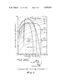
- FIG. 2 is a graph illustrating the spectral response of various photoemissive materials sensitive to visible and near infrared radiation as a function of the irradiating wavelength, with appropriate stimulating laser wavelengths indicated;
- FIG. 3 is a cross-sectional side view of a photoemissive cathode disclosed herein;
- FIG. 4 illustrates a method of fabricating the photoemissive cathode of FIG. 3 for lithographic applications
- FIG. 5 is a cross-sectional side view of a photoemissive cathode of the invention which is equipped with a liquid cooler;
- FIG. 6 is a graph illustrating the current densities achieved in tests of a photoemissive cathode of the invention as a function of time.
- FIGS. 7 and 8 are schematic representations of portions of electron beam generators illustrating alternate embodiments of the invention.
- FIG. 1 is a schematic representation of an electron beam lithography system employing a back-illuminable, laser-irradiable photoemissive electron source according to a preferred embodiment of the invention.
- the system includes a laser 10 such as an argon ion laser, which is operable to generate a beam of coherent light at one of several radiating frequencies of 454.5, 457.9, 465.8, 472.7, 476.5. 488.0, 496.5, 501.7, and 514.5 nanometers. The strongest radiating frequencies are 488.0 and 514.5 nanometers.
- a suitable laser is a series 550 argon ion laser available from Control Laser Corporation of Orlando, Fla.
- the modulator 11 Positioned in the lasing cavity of the laser 10 or at another location near the laser is a beam modulator 11.
- the modulator 11 may be any electro-optical or acousto-optical device suitable for regulating the intensity of the beam or deflecting it. Such devices are well known and are commercially available as units having a modulation rate of at least several megahertz, a rate essential for achieving fast writing times (high throughput) in direct-write lithography applications.
- Acousto-optical modulators may comprise tellurium dioxide or lead molybdate crystals having a high contrast ratio and rapid rise time (10-20 nanoseconds) and which deflect the laser beam by interaction of the beam with acoustic waves produced in the crystals.
- An advantage of such devices over other modulators is their relatively low operating voltage and power consumption.
- One acousto-optical modulator suitable for use with the present invention is a Lead Molybdate Modulator Model 1250C, available from Isomet of Springfield, Va.
- Electro-optical modulators include electro-optical materials such as potassium dihydrogen phosphate (KDP) or ammonium dihydrogen phosphate (ADP) which generate birefringence when an electrical field is applied to the material.
- KDP potassium dihydrogen phosphate
- ADP ammonium dihydrogen phosphate
- the birefringence produces a change in polarization of a beam passing through the electro-optical material, and external polarizers included in the modulator then pass a beam whose intensity varies with the applied voltage.
- An electro-optical modulator suitable for use with the present invention is a low voltage modulator Model 3030 available from Lasermetrics, Inc. of Teaneck, N.J.
- the light beam radiating from the laser 10 is guided by a light optical train 12 including a plate 13 having an aperture 14 of specified geometry, for example, a square.
- a lens 15 focuses the laser light as an image of the aperture 14 onto a photoemissive cathode 16 which will be described in detail hereinafter.
- the photoemissive cathode 16 and electron optical components for processing the electrons emitted by the cathode 16 are housed within a vacuum chamber schematically illustrated by the dotted enclosure 18.
- a high vacuum such as a pressure of 10 -9 torr or less is maintained in the vacuum chamber 18.
- anode 20 On the opposite side of the photoemissive cathode 16 from the laser 10 is an anode 20 which operates to accelerate electrons emitted by the cathode 16.
- An additional negatively charged Wehnelt electrode (not shown) may be positioned between the photoemissive cathode 16 and the anode 20.
- the electron beam From the anode 20 the electron beam next passes through various known electron optical components, which shape and position the electron beam as it is directed towards a target 21. After being accelerated by the anode 20, the electron beam passes through an electron lens 22 and then through an electrostatic beam-shaped deflector 26 and a beam-shaping aperture 28.
- the beam-shaping deflector 26 operates to alter the position of the electron image of the photoemissive electron source on the beam-shaping aperture 28 to create a variably shaped and sized electron beam.
- the beam next passes through a demagnification lens 29, and subsequently through a beam-limiting aperture 30.
- Immersed in a final projection lens 32 are dynamic focussing coils 34 which focus the beam onto the target 21, dynamic stigmators 36 which provide astigmatic correction to the beam, and a deflection yoke 38 which scans the beam over the target.
- the electron beam intensity can be modulated by modulating the laser beam intensity. Modulation of this optical beam is facilitated by location of the beam modulator 11 outside of the high vacuum chamber 18. In prior art lithographic electron beam devices, beam modulation is accomplished by special blanking electrodes which must be located between an electron source and a target within a vacuum enclosure.
- the lithography system of the present invention takes advantage of the general proposition that replacing any component located in the vacuum enclosure by a similar functional element positioned outside the vacuum enclosure simplifies the overall lithographic column fabrication and operation.
- the photoemissive cathode 16 includes a photoemissive surface formed, for example, of cesium antimonide, Cs 3 Sb, which emits electrons when illuminated by the argon ion laser light.
- FIG. 2 is a graph of the spectral response (milliamperes of electron current per watt of illuminating radiation) of various photoemissive materials as a function of the wavelength of illumination. Note that at the strongest argon ion laser illuminating wavelengths of 488.0 and 514.5 nanometers, cesium antimonide has high sensitivities with quantum efficiencies of 6 percent or more.
- Another suitable photoemissive surface for the cathode 16 is the "bialkali” sodium potassium antimonide (Na 2 KSb) photocathode.
- Na 2 KSb sodium potassium antimonide
- the preferred method of making the Na 2 KSb photocathode is basically similar to that to be described hereinafter for Cs 3 Sb, and the spectral response of these two surfaces is similar as is indicated in FIG. 2. Consequently, the Na 2 KSb photocathode is also sensitive to argon ion laser irradiation.
- photoemissive surfaces may be formed from single crystals composed of elements from groups III and V of the Periodic Table such as gallium, phosphorus, and arsenic coated with either cesium or cesium and oxygen. Such surfaces can be made to have a negative electron affinity and therefore substantially increased electron escape depths. This characteristic results in an emission of electrons with especially low energy spread.
- gallium phosphide GaP
- gallium arsenide phosphide Ga(As x P 1-x )
- a single crystal transmissive layer of GaP is first grown on a substrate optically transparent to the irradiating laser.
- the GaP is then activated with cesium.
- Another suitable photoemissive surface is gallium arsenside coated with cesium and oxygen (GaAs(Cs,O)).
- An argon ion laser, an appropriate semiconductor injection laser, or a suitably intense LED can be used to stimulate electron emission.
- the argon ion laser emits light at a wavelength near the optimum quantum efficiency for photoemissive surfaces of gallium phosphide, gallium arsenide, and gallium arsenide phosphide, thereby maximizing the emission of electrons.
- An injection laser such as a gallium aluminum arsenide ((GaAl)As) infrared injection laser used in combination with a GaAs(Cs,O) photoemissive surface will emit radiation at much lower power levels but can be constructed to operate near the long wavelength threshold of these photoemissive materials, e.g. at about 900 nanometers, thereby minimizing the emitted electron energy spread.
- injection lasers are typically current-driven devices, modulation of their output beam may be achieved by modulating the current input to the injection laser rather than by means of a separate electro-optical or acousto-optical device.
- a gallium aluminum arsenide injection laser suitable for use in the present invention is a CW injection laser Model No. C86030E available from RCA of Lancaster, Pa., which is modulated by a variable current input.
- LED's Light-emitting diodes have properties similar to injection lasers but their output is less monochromatic, resulting in a somewhat larger energy spread of the emitted electrons.
- the photoemissive cathode 16 includes a light transmissive substrate 40 which is preferably quartz or sapphire but which also may be glass.
- a thick metallic coating 42 is deposited onto one side of the substrate 40. Suitable materials are, for example, chromium, tungsten, aluminum, nickel, and mixtures of these metals.
- the layer 42 does not extend into a central region 44, a structure achieved by keeping the region 44 masked during deposition of the coating 42.
- a thin semitransparent electrically conducting layer 46 of, for example, chromium and nickel is next deposited on top of the layer 42 and the region 44.
- This electrically conducting layer may not be necessary for cathodes which utilize gallium phosphide, gallium arsenide phosphide or gallium arsenide as photoemissive surfaces.
- a layer 48 of the photoemissive material, such as cesium antimonide, is produced within the region 44.
- a suitable transparent substrate 40 such as quartz, sapphire or glass is selected and heated to about 300° C. by means of a nichrome heater wire 58 wrapped around the periphery of the substrate 40.
- a coating 42 of, for example, chromium or chromium and nickel, sufficiently thick (e.g., about 2000 angstroms) to allow the attachment of external electrical leads and to act as a low resistance electrical path to the central region 44.
- the thick coating 42 has the function of readily conducting electrons from an external power source to the central region 44, and it also conducts heat away from the central region 44.
- Deposition of the thick coating 42 may be performed by evaporating chromium and nickel from a resistance-heated nichrome wire 52.
- the central region 44 which may have an area of approximately 0.02 square millimeters or more (or may have a smaller area to facilitate production of electron beams with very high current densities) is masked to prevent the thick layer of chromium and nickel from being deposited in the region 44. Thereafter the mask is removed and the substrate 40 with the thick coating 42 is heated to about 500° C. to remove surface contaminants. This heating step has been found to improve the adherence of the coating 42 to the substrate 40. Then the temperature is reduced to about 300° C.
- a thin electrically conductive, optically semitransparent layer 46 of chromium and nickel is deposited in vacuum on the entire selected substrate side including the previously masked central region 44.
- This chromium and nickel may also be supplied by the nichrome wire 52, resistance heated to evaporate these elements onto the substrate 40.
- the nichrome wire 52 is heated until the electrically conductive, optically semitransparent chromium and nickel layer 46 is deposited in the region 44.
- a suitable thickness for this thin layer 46 of chromium and nickel is about 100 angstroms or less; such a layer 46 will reduce the transmission of visible light through the central region 44 to, for example, between 40 and 50% of that passing through the transparent substrate 40.
- the thin layer 46 serves as an electrical path between the thick annular coating 42 and the central region 44.
- the temperature of the substrate 40 with the thick coating 42 and the thin coating 46 is reduced to about 130° C. and an antimony bead 54 melted onto a nichrome supporting wire 56 is resistance heated in vacuum so as to evaporate a thin layer of antimony onto the portion of the layer 46 in the region 44. Evaporation of antimony onto the part of the chromium and nickel layer 46 outside of the central region 44 will not affect the photoemissive behavior of the system.
- the thickness of the antimony film should be such as to reduce the overall transmission of visible light in the central region 44 to, for example, about 30 to 40% of that passing through the transparent substrate 40.
- the substrate 40 with the chromium and nickel coating and the antimony coating and kept under vacuum is positioned in a high vacuum chamber 50 pumped to pressures below 2 ⁇ 10 -9 torr which is, or will become, that component of the lithography column containing the photoemissive cathode 16.
- the substrate 40 in the high vacuum chamber 50 is then heated to approximately 100° C. by the nichrome heater wire 58 wrapped around the periphery of the substrate 40.
- a cesium source "channel" 60 which contains, for example, a mixture of cesium chromate and a reducing agent such as silicon.
- the channel 60 is resistance-heated by means of an electrical connecting wire 62 to evaporate pure cesium onto the heated antimony film in the region 44.
- Evaporation of cesium onto the antimony film or chromium layer outside the region 44 will not affect the photoemissive behavior of the system. In this way a thin layer or film 48 of cesium antimonide is produced in the region 44. Overall thickness of the thin layer 48 may, for example, be about 400 angstroms.
- the photoemissive cathode 16 is illuminated by, for example, the argon ion laser and the photon-generated current is measured by collecting the emitted electrons on the nichrome wire 52.
- the currents through the wire 62 and through the substrate-heating nichrome heater wire 58 are stopped so that no more cesium is deposited in the region 44. Should the photocurrent drop during cooling of the substrate, additional cesium is evaporated onto the cold surface 44. If the additional cesium evaporated onto the region 44 does not cause the photocurrent to return to its maximum value, more antimony may be evaporated onto the substrate followed by the deposition of additional cesium until a maximum value is attained.
- the Cs 3 Sb cathode may degrade due to the loss of cesium and contamination by impurities. Such degradation can be reversed by additional evaporation of antimony and cesium onto the region 44 as detailed above.
- a laser beam from the laser 10 such as an argon ion laser, passes through the transparent substrate 40 and through the semitransparent chromium and nickel layer 46 and penetrates into the cesium antimonide layer 48, causing electrons to be emitted from the cesium antimonide.
- the electron beam thus emitted from the photoemissive cathode 16 has a high current density--for example, current densities in excess of 3 amperes per square centimeter have been achieved utilizing photoemissive films of cesium antimonide having an area of 4.8 ⁇ 10 -5 square centimeters and operated as substantially a point source--i.e., with an argon ion laser beam focussed on this very small area on the film.
- the photoemissive cathodes of the invention inherently operate as "cold" electron sources, for efficient, long life operation at high current density levels it is desirable that the electron beam generator systems disclosed herein be equipped with cooling devices to maintain the temperature of the photocathode near or below room temperature.
- a photoemissive cathode 16 is enclosed in a housing 64 of conductive material such as stainless steel, and a cooler 66 is attached to the outside surface of the housing 64.
- the cooler 66 shown comprises a water-filled coil.
- any other suitable cooling device can be used.
- One preferred cooler is a thermoelectric cooler, a well known, electrically-powered device which offers the advantages of being compact, reliable, and not containing moving parts or fluid connections.
- a photoemissive cathode similar to that shown in FIG. 5 was tested in combination with an argon ion laser.
- the photocathode 16 included a sapphire disk 0.25 inches in diameter and 0.1 inch thick held within a stainless steel housing 64 by means of a nut 68 and a washer 70.
- the housing in turn was wrapped with a heating coil 72 and a liquid cooling tube 66 connected to a source of water, both the coil 72 and the tube 66 being brazed to the outside surface 74 of the housing 64.
- Ni/Cr nickel/chromium
- a D.C. power source 80 was electrically connected to the stainless steel housing 64 to provide a flow of electrons to the annular coating 42 and in turn to the thin Ni/Cr layer and the photoemissive layer 48 in the central region 44.
- the positive terminal of the power source 80 was connected to a collector anode 82 spaced approximately 0.1 inches from the front surface of the sapphire substrate 40.
- the photocathode 16 was back-illuminated by a continuous, unmodulated beam from an argon ion laser operated for test periods totaling up to about 100 hours.
- Test runs were made at several laser power settings and illuminating wavelengths, various collector potentials, and at various photocathode temperatures and sizes of the central area. Only an indirect indication of photocathode temperatures was available during the tests since temperatures recorded were those (generally lower) values of the housing.
- FIGS. 7 and 8 are schematic representations of portions of alternate embodiments of portions of an electron beam generator particularly adapted for use with an injection laser.
- a cooling device such as a finned thermoelectric cooler 110 may be provided to cool both the laser 94 and the photoemissive cathode 90.
- the photoemissive cathode 104 shown in FIG. 8 is coated onto one end of an optical fiber 106 of material suitable for low-loss transmission of the beam of a laser.
- a suitable fiber is Telecommunication fiber Model MG 05, available from Valtec of West Boylston, Mass.
- the opposite end of the fiber 106 is connected to the output facet 107 of an injection laser 108 to receive its output beam.
- the injection laser 108 may be positioned inside a cooling device such as a thermoelectric cooler 110.
- a photoemissive cathode 16 which, when back-illuminated through a chromium and nickel layer with 50 to 60% optical loss, has a quantum efficiency of 3% or more and which upon degradation may be easily restored in situ by the deposition of additional cesium or cesium and antimony.
- the photoemissive cathode 16 is capable of generating a high current density of up to three amperes per square centimeter or greater to provide current densities at a target 21 of hundreds of amperes per square centimeter.
- the maximum energy of the emitted electrons is dependent on the difference of the laser's photon energy and the electron emission threshold energy, defined by an electronic transition between the top of the photoemissive material's valence band and its vacuum level.
- the maximum emission energy of the electrons is 0.43 electron volts, which is, therefore, the maximum energy spread of the electrons.
- the nominal energy spread commonly based on the half-width of the distribution curve of numbers of emitted electrons versus their energy is substantially lower than this.
- the cathode operates at a low temperature such as room temperature so that there are no support problems as would be the case with a heated cathode. Furthermore, no heating-up time is required because the electrons are generated instantaneously in response to illumination by the laser light. Modulation of the electron beam can conveniently be accomplished by modulating the laser beam outside the vacuum chamber 18. In addition, beam shaping or patterning into complex shapes is easily accomplished by apertures or masks in the optical train between the laser 10 and the photoemissive cathode 16 outside of the vacuum enclosure 18.
Abstract
Description
              TABLE 1
______________________________________
                               Housing
                                      Peak
     Laser      Laser   Collector
                               Temper-
                                      Current
Run  Wavelength Power   Potential
                               ature  Density
No.  (Angstroms)
                (Watts) (Volts)
                               (°C.)
                                      (Amps/Cm.sup.2)
______________________________________
1    4765       0.2      100   48     .02
2    4765       0.3      150   20     .03
3    4880       0.5     1000    6     3.0
______________________________________
Claims (22)
Priority Applications (1)
| Application Number | Priority Date | Filing Date | Title |
|---|---|---|---|
| US06/525,514 US4460831A (en) | 1981-11-30 | 1983-08-22 | Laser stimulated high current density photoelectron generator and method of manufacture |
Applications Claiming Priority (2)
| Application Number | Priority Date | Filing Date | Title |
|---|---|---|---|
| US32596081A | 1981-11-30 | 1981-11-30 | |
| US06/525,514 US4460831A (en) | 1981-11-30 | 1983-08-22 | Laser stimulated high current density photoelectron generator and method of manufacture |
Related Parent Applications (1)
| Application Number | Title | Priority Date | Filing Date |
|---|---|---|---|
| US32596081A Continuation-In-Part | 1981-11-30 | 1981-11-30 |
Publications (1)
| Publication Number | Publication Date |
|---|---|
| US4460831A true US4460831A (en) | 1984-07-17 |
Family
ID=26985184
Family Applications (1)
| Application Number | Title | Priority Date | Filing Date |
|---|---|---|---|
| US06/525,514 Expired - Lifetime US4460831A (en) | 1981-11-30 | 1983-08-22 | Laser stimulated high current density photoelectron generator and method of manufacture |
Country Status (1)
| Country | Link |
|---|---|
| US (1) | US4460831A (en) |
Cited By (80)
| Publication number | Priority date | Publication date | Assignee | Title |
|---|---|---|---|---|
| US4554458A (en) * | 1983-08-11 | 1985-11-19 | International Business Machines Corporation | Electron beam projection lithography |
| US4820927A (en) * | 1985-06-28 | 1989-04-11 | Control Data Corporation | Electron beam source employing a photo-emitter cathode |
| DE3741124A1 (en) * | 1987-12-04 | 1989-06-15 | Nmi Naturwissenschaftl U Mediz | Electron beam nanolithographic system having a multiple-beam electron source capable of multiplex control and made from MIM (metal-insulator-metal) thin-film cathodes |
| US4906894A (en) * | 1986-06-19 | 1990-03-06 | Canon Kabushiki Kaisha | Photoelectron beam converting device and method of driving the same |
| US4970392A (en) * | 1990-01-17 | 1990-11-13 | Thermo Electron Corporation | Stably emitting demountable photoelectron generator |
| US5023462A (en) * | 1988-03-23 | 1991-06-11 | Fujitsu Limited | Photo-cathode image projection apparatus for patterning a semiconductor device |
| US5039862A (en) * | 1990-02-20 | 1991-08-13 | Smith Donald O | Switched electron beam source employing a common photo-emitter cathode and method of operation |
| US5142193A (en) * | 1989-06-06 | 1992-08-25 | Kaman Sciences Corporation | Photonic cathode ray tube |
| US5339737A (en) * | 1992-07-20 | 1994-08-23 | Presstek, Inc. | Lithographic printing plates for use with laser-discharge imaging apparatus |
| US5351617A (en) * | 1992-07-20 | 1994-10-04 | Presstek, Inc. | Method for laser-discharge imaging a printing plate |
| US5353705A (en) * | 1992-07-20 | 1994-10-11 | Presstek, Inc. | Lithographic printing members having secondary ablation layers for use with laser-discharge imaging apparatus |
| US5379698A (en) * | 1992-07-20 | 1995-01-10 | Presstek, Inc. | Lithographic printing members for use with laser-discharge imaging |
| US5385092A (en) * | 1992-07-20 | 1995-01-31 | Presstek, Inc. | Laser-driven method and apparatus for lithographic imaging |
| WO1997003453A2 (en) * | 1995-07-10 | 1997-01-30 | Intevac, Inc. | Electron sources utilizing negative electron affinity photocathodes with ultra-small emission areas |
| USRE35512E (en) * | 1992-07-20 | 1997-05-20 | Presstek, Inc. | Lithographic printing members for use with laser-discharge imaging |
| WO1998054750A1 (en) * | 1997-05-27 | 1998-12-03 | The Board Of Trustees Of The Leland Stanford Junior University | Electron sources having shielded cathodes |
| WO1999030348A1 (en) * | 1997-12-09 | 1999-06-17 | Intevac, Inc. | Electron sources utilizing patterned negative electron affinity photocathodes |
| WO1999050874A2 (en) * | 1998-03-31 | 1999-10-07 | Etec Systems, Inc. | Gated photocathode for controlled single and multiple electron beam emission |
| US6005247A (en) * | 1997-10-01 | 1999-12-21 | Intevac, Inc. | Electron beam microscope using electron beam patterns |
| US6005882A (en) * | 1997-11-18 | 1999-12-21 | Hyde, Jr.; James R. | Electron pump |
| US6087047A (en) * | 1997-12-19 | 2000-07-11 | Hoya Corporation | Phase shift mask and phase shift mask blank |
| US6215128B1 (en) * | 1999-03-18 | 2001-04-10 | Etec Systems, Inc. | Compact photoemission source, field and objective lens arrangement for high throughput electron beam lithography |
| US6236154B1 (en) * | 1998-03-04 | 2001-05-22 | U.S. Philips Corporation | Electron tube with a cesium source |
| US6448568B1 (en) * | 1999-07-30 | 2002-09-10 | Applied Materials, Inc. | Electron beam column using high numerical aperture photocathode source illumination |
| US6476401B1 (en) | 1999-09-16 | 2002-11-05 | Applied Materials, Inc. | Moving photocathode with continuous regeneration for image conversion in electron beam lithography |
| US20030122091A1 (en) * | 2001-11-07 | 2003-07-03 | Gilad Almogy | Maskless photon-electron spot-grid array printer |
| US20030178583A1 (en) * | 2000-09-18 | 2003-09-25 | Kampherbeek Bert Jan | Field emission photo-cathode array for lithography system and lithography system provided with such an array |
| US6693282B1 (en) * | 1999-06-22 | 2004-02-17 | Fei Company | Particle-optical apparatus including a particle source that can be switched between high brightness and large beam current |
| EP1403898A2 (en) | 2002-09-26 | 2004-03-31 | LEO Elektronenmikroskopie GmbH | Electron beam source, electron-optical apparatus comprising an electron beam source and method of operating an electron beam source |
| US20040069960A1 (en) * | 2002-10-10 | 2004-04-15 | Applied Materials, Inc. | Electron beam pattern generator with photocathode comprising low work function cesium halide |
| US6724002B2 (en) * | 2001-01-31 | 2004-04-20 | Applied Materials, Inc. | Multiple electron beam lithography system with multiple beam modulated laser illumination |
| US20040108812A1 (en) * | 2002-12-10 | 2004-06-10 | Applied Materials, Inc. | Current-stabilizing illumination of photocathode electron beam source |
| US20040232357A1 (en) * | 2001-01-31 | 2004-11-25 | Andres Fernadez | Electron beam lithography system having improved electron gun |
| US6828574B1 (en) | 2000-08-08 | 2004-12-07 | Applied Materials, Inc. | Modulator driven photocathode electron beam generator |
| US20060028114A1 (en) * | 2003-02-14 | 2006-02-09 | Stijn Willem Herman Steenbrink | Dispenser cathode |
| US7015467B2 (en) | 2002-10-10 | 2006-03-21 | Applied Materials, Inc. | Generating electrons with an activated photocathode |
| US20070228286A1 (en) * | 2006-03-30 | 2007-10-04 | Lewellen John W | Polarized pulsed front-end beam source for electron microscope |
| US7311406B2 (en) * | 1993-02-26 | 2007-12-25 | Donnelly Corporation | Image sensing system for a vehicle |
| US7388182B2 (en) | 1993-02-26 | 2008-06-17 | Donnelly Corporation | Image sensing system for controlling an accessory or headlight of a vehicle |
| US20080169436A1 (en) * | 2007-01-11 | 2008-07-17 | Kla-Tencor Techologies Corporation | Electron beam lithography method and apparatus using a dynamically controlled photocathode |
| US7526103B2 (en) | 2004-04-15 | 2009-04-28 | Donnelly Corporation | Imaging system for vehicle |
| US7655894B2 (en) | 1996-03-25 | 2010-02-02 | Donnelly Corporation | Vehicular image sensing system |
| US20100075259A1 (en) * | 2005-09-15 | 2010-03-25 | Franklin Mark Schellenberg | Illuminating waveguide fabrication method |
| US7859565B2 (en) | 1993-02-26 | 2010-12-28 | Donnelly Corporation | Vision system for a vehicle including image processor |
| US7972045B2 (en) | 2006-08-11 | 2011-07-05 | Donnelly Corporation | Automatic headlamp control system |
| US8017898B2 (en) | 2007-08-17 | 2011-09-13 | Magna Electronics Inc. | Vehicular imaging system in an automatic headlamp control system |
| US8063759B2 (en) | 1993-02-26 | 2011-11-22 | Donnelly Corporation | Vehicle vision system |
| US8070332B2 (en) | 2007-07-12 | 2011-12-06 | Magna Electronics Inc. | Automatic lighting system with adaptive function |
| US8189871B2 (en) | 2004-09-30 | 2012-05-29 | Donnelly Corporation | Vision system for vehicle |
| US8217830B2 (en) | 2007-01-25 | 2012-07-10 | Magna Electronics Inc. | Forward facing sensing system for a vehicle |
| US8446470B2 (en) | 2007-10-04 | 2013-05-21 | Magna Electronics, Inc. | Combined RGB and IR imaging sensor |
| US8451107B2 (en) | 2007-09-11 | 2013-05-28 | Magna Electronics, Inc. | Imaging system for vehicle |
| US8643724B2 (en) | 1996-05-22 | 2014-02-04 | Magna Electronics Inc. | Multi-camera vision system for a vehicle |
| US8665079B2 (en) | 2002-05-03 | 2014-03-04 | Magna Electronics Inc. | Vision system for vehicle |
| US8874317B2 (en) | 2009-07-27 | 2014-10-28 | Magna Electronics Inc. | Parking assist system |
| US8886401B2 (en) | 2003-10-14 | 2014-11-11 | Donnelly Corporation | Driver assistance system for a vehicle |
| US8890955B2 (en) | 2010-02-10 | 2014-11-18 | Magna Mirrors Of America, Inc. | Adaptable wireless vehicle vision system based on wireless communication error |
| US9014904B2 (en) | 2004-12-23 | 2015-04-21 | Magna Electronics Inc. | Driver assistance system for vehicle |
| US9041806B2 (en) | 2009-09-01 | 2015-05-26 | Magna Electronics Inc. | Imaging and display system for vehicle |
| US9085261B2 (en) | 2011-01-26 | 2015-07-21 | Magna Electronics Inc. | Rear vision system with trailer angle detection |
| US9117123B2 (en) | 2010-07-05 | 2015-08-25 | Magna Electronics Inc. | Vehicular rear view camera display system with lifecheck function |
| US9126525B2 (en) | 2009-02-27 | 2015-09-08 | Magna Electronics Inc. | Alert system for vehicle |
| US9191574B2 (en) | 2001-07-31 | 2015-11-17 | Magna Electronics Inc. | Vehicular vision system |
| US9245448B2 (en) | 2001-07-31 | 2016-01-26 | Magna Electronics Inc. | Driver assistance system for a vehicle |
| US9264672B2 (en) | 2010-12-22 | 2016-02-16 | Magna Mirrors Of America, Inc. | Vision display system for vehicle |
| US9263228B2 (en) | 2014-03-10 | 2016-02-16 | International Business Machines Corporation | Integrated photoemission sources and scalable photoemission structures |
| US9446713B2 (en) | 2012-09-26 | 2016-09-20 | Magna Electronics Inc. | Trailer angle detection system |
| US20160307726A1 (en) * | 2011-03-15 | 2016-10-20 | Ebara Corporation | Inspection device |
| US9495876B2 (en) | 2009-07-27 | 2016-11-15 | Magna Electronics Inc. | Vehicular camera with on-board microcontroller |
| US9509957B2 (en) | 2008-07-24 | 2016-11-29 | Magna Electronics Inc. | Vehicle imaging system |
| US9558409B2 (en) | 2012-09-26 | 2017-01-31 | Magna Electronics Inc. | Vehicle vision system with trailer angle detection |
| US9900522B2 (en) | 2010-12-01 | 2018-02-20 | Magna Electronics Inc. | System and method of establishing a multi-camera image using pixel remapping |
| US10132971B2 (en) | 2016-03-04 | 2018-11-20 | Magna Electronics Inc. | Vehicle camera with multiple spectral filters |
| US10160382B2 (en) | 2014-02-04 | 2018-12-25 | Magna Electronics Inc. | Trailer backup assist system |
| US20190295804A1 (en) * | 2018-03-20 | 2019-09-26 | Kla-Tencor Corporation | System and Method for Photocathode Illumination Inspection |
| US10875403B2 (en) | 2015-10-27 | 2020-12-29 | Magna Electronics Inc. | Vehicle vision system with enhanced night vision |
| US20210050174A1 (en) * | 2018-03-23 | 2021-02-18 | Freemelt Ab | Cathode assembly for electron gun |
| WO2021123080A1 (en) * | 2019-12-20 | 2021-06-24 | Asml Netherlands B.V. | Beam current adjustment for charged-particle inspection system |
| CN113594002A (en) * | 2021-07-06 | 2021-11-02 | 北方夜视技术股份有限公司 | Optical fiber window multi-alkali cathode and manufacturing method thereof |
| CN115326044A (en) * | 2022-10-14 | 2022-11-11 | 天津集智航宇科技有限公司 | Laser gyroscope and sealing method thereof |
Citations (13)
| Publication number | Priority date | Publication date | Assignee | Title |
|---|---|---|---|---|
| GB966442A (en) * | 1961-11-09 | 1964-08-12 | Trub Tauber & Co A G | Improvements in and relating to electron-emission microscopes |
| US3408521A (en) * | 1965-11-22 | 1968-10-29 | Stanford Research Inst | Semiconductor-type photocathode for an infrared device |
| US3575628A (en) * | 1968-11-26 | 1971-04-20 | Westinghouse Electric Corp | Transmissive photocathode and devices utilizing the same |
| US3585433A (en) * | 1968-04-29 | 1971-06-15 | Westinghouse Electric Corp | Masked photocathode with first and second metallic patterns |
| GB1336626A (en) * | 1971-12-13 | 1973-11-07 | Mullard Ltd | Methods of manufacturing semiconductor devices |
| US3814964A (en) * | 1973-01-19 | 1974-06-04 | Ace Sophisticates Inc | External photodetector cooling techniques |
| GB1467521A (en) * | 1973-06-13 | 1977-03-16 | Westinghouse Electric Corp | Method and apparatus for electron beam alignment with a member by detecting cathodoluminescence from oxide layers for fabricating circuit patterns |
| US4039810A (en) * | 1976-06-30 | 1977-08-02 | International Business Machines Corporation | Electron projection microfabrication system |
| US4097761A (en) * | 1966-02-16 | 1978-06-27 | Rca Corporation | Image tube cathode |
| US4115223A (en) * | 1975-12-15 | 1978-09-19 | International Standard Electric Corporation | Gallium arsenide photocathodes |
| US4213053A (en) * | 1978-11-13 | 1980-07-15 | International Business Machines Corporation | Electron beam system with character projection capability |
| US4227090A (en) * | 1979-02-21 | 1980-10-07 | Hughes Aircraft Company | Electron beam microfabrication apparatus and method |
| US4286373A (en) * | 1980-01-08 | 1981-09-01 | The United States Of America As Represented By The Secretary Of The Army | Method of making negative electron affinity photocathode |
-
1983
- 1983-08-22 US US06/525,514 patent/US4460831A/en not_active Expired - Lifetime
Patent Citations (13)
| Publication number | Priority date | Publication date | Assignee | Title |
|---|---|---|---|---|
| GB966442A (en) * | 1961-11-09 | 1964-08-12 | Trub Tauber & Co A G | Improvements in and relating to electron-emission microscopes |
| US3408521A (en) * | 1965-11-22 | 1968-10-29 | Stanford Research Inst | Semiconductor-type photocathode for an infrared device |
| US4097761A (en) * | 1966-02-16 | 1978-06-27 | Rca Corporation | Image tube cathode |
| US3585433A (en) * | 1968-04-29 | 1971-06-15 | Westinghouse Electric Corp | Masked photocathode with first and second metallic patterns |
| US3575628A (en) * | 1968-11-26 | 1971-04-20 | Westinghouse Electric Corp | Transmissive photocathode and devices utilizing the same |
| GB1336626A (en) * | 1971-12-13 | 1973-11-07 | Mullard Ltd | Methods of manufacturing semiconductor devices |
| US3814964A (en) * | 1973-01-19 | 1974-06-04 | Ace Sophisticates Inc | External photodetector cooling techniques |
| GB1467521A (en) * | 1973-06-13 | 1977-03-16 | Westinghouse Electric Corp | Method and apparatus for electron beam alignment with a member by detecting cathodoluminescence from oxide layers for fabricating circuit patterns |
| US4115223A (en) * | 1975-12-15 | 1978-09-19 | International Standard Electric Corporation | Gallium arsenide photocathodes |
| US4039810A (en) * | 1976-06-30 | 1977-08-02 | International Business Machines Corporation | Electron projection microfabrication system |
| US4213053A (en) * | 1978-11-13 | 1980-07-15 | International Business Machines Corporation | Electron beam system with character projection capability |
| US4227090A (en) * | 1979-02-21 | 1980-10-07 | Hughes Aircraft Company | Electron beam microfabrication apparatus and method |
| US4286373A (en) * | 1980-01-08 | 1981-09-01 | The United States Of America As Represented By The Secretary Of The Army | Method of making negative electron affinity photocathode |
Non-Patent Citations (10)
| Title |
|---|
| AR . C. K. Sinclair et al, A High Intensity Polarized Electron Source for the Stanford Linear Accelerator , High Energy Physics with Polarized Beams and Targets A.I.P. Conference Proceedings No. 35, 1976. * |
| AR". C. K. Sinclair et al, "A High Intensity Polarized Electron Source for the Stanford Linear Accelerator", High Energy Physics with Polarized Beams and Targets A.I.P. Conference Proceedings No. 35, 1976. |
| AR. R. K. Watts and J. H. Bruning, "A Review of Fine-Line Lithographic Techniques: Present and Future", Solid State Technology, May 1981, pp. 99-105. |
| AR. R. K. Watts and J. H. Bruning, A Review of Fine Line Lithographic Techniques: Present and Future , Solid State Technology, May 1981, pp. 99 105. * |
| AS . C. K. Sinclair, High Intensity Polarized Electron Sources , Nuclear Instrumentation, 1980. * |
| AS'. C. K. Sinclair, "High Intensity Polarized Electron Sources", Nuclear Instrumentation, 1980. |
| AS. T. H. P. Chang et al, "Electron-Beam Lighography Draws a Finer Line", Electronics, May 12, 1977, pp. 89-98. |
| AS. T. H. P. Chang et al, Electron Beam Lighography Draws a Finer Line , Electronics, May 12, 1977, pp. 89 98. * |
| AT. J. C. Edison et al, "A Precision High-Speed Electron Beam Lithography System"; J. Kelly et al, "a Precision, High-Current, High-Speed Electron Beam Lithography Column"; and E. A. Lindbert et al, "A Precision X-Y Stage and Substrate Handling System for Electron Beam Lithography", Hewlett-Packard Journal, May 1981, pp. 1-20. |
| AT. J. C. Edison et al, A Precision High Speed Electron Beam Lithography System ; J. Kelly et al, a Precision, High Current, High Speed Electron Beam Lithography Column ; and E. A. Lindbert et al, A Precision X Y Stage and Substrate Handling System for Electron Beam Lithography , Hewlett Packard Journal, May 1981, pp. 1 20. * |
Cited By (255)
| Publication number | Priority date | Publication date | Assignee | Title |
|---|---|---|---|---|
| US4554458A (en) * | 1983-08-11 | 1985-11-19 | International Business Machines Corporation | Electron beam projection lithography |
| US4820927A (en) * | 1985-06-28 | 1989-04-11 | Control Data Corporation | Electron beam source employing a photo-emitter cathode |
| US4906894A (en) * | 1986-06-19 | 1990-03-06 | Canon Kabushiki Kaisha | Photoelectron beam converting device and method of driving the same |
| DE3741124A1 (en) * | 1987-12-04 | 1989-06-15 | Nmi Naturwissenschaftl U Mediz | Electron beam nanolithographic system having a multiple-beam electron source capable of multiplex control and made from MIM (metal-insulator-metal) thin-film cathodes |
| US5023462A (en) * | 1988-03-23 | 1991-06-11 | Fujitsu Limited | Photo-cathode image projection apparatus for patterning a semiconductor device |
| US5142193A (en) * | 1989-06-06 | 1992-08-25 | Kaman Sciences Corporation | Photonic cathode ray tube |
| US4970392A (en) * | 1990-01-17 | 1990-11-13 | Thermo Electron Corporation | Stably emitting demountable photoelectron generator |
| US5039862A (en) * | 1990-02-20 | 1991-08-13 | Smith Donald O | Switched electron beam source employing a common photo-emitter cathode and method of operation |
| US5339737A (en) * | 1992-07-20 | 1994-08-23 | Presstek, Inc. | Lithographic printing plates for use with laser-discharge imaging apparatus |
| US5351617A (en) * | 1992-07-20 | 1994-10-04 | Presstek, Inc. | Method for laser-discharge imaging a printing plate |
| US5353705A (en) * | 1992-07-20 | 1994-10-11 | Presstek, Inc. | Lithographic printing members having secondary ablation layers for use with laser-discharge imaging apparatus |
| US5379698A (en) * | 1992-07-20 | 1995-01-10 | Presstek, Inc. | Lithographic printing members for use with laser-discharge imaging |
| US5385092A (en) * | 1992-07-20 | 1995-01-31 | Presstek, Inc. | Laser-driven method and apparatus for lithographic imaging |
| USRE35512E (en) * | 1992-07-20 | 1997-05-20 | Presstek, Inc. | Lithographic printing members for use with laser-discharge imaging |
| US7311406B2 (en) * | 1993-02-26 | 2007-12-25 | Donnelly Corporation | Image sensing system for a vehicle |
| US8599001B2 (en) | 1993-02-26 | 2013-12-03 | Magna Electronics Inc. | Vehicular vision system |
| US7325935B2 (en) | 1993-02-26 | 2008-02-05 | Donnelly Corporation | Image sensing system for a vehicle |
| US7344261B2 (en) | 1993-02-26 | 2008-03-18 | Donnelly Corporation | Vehicular vision system |
| US7380948B2 (en) | 1993-02-26 | 2008-06-03 | Donnelly Corporation | Image sensing system for a vehicle |
| US7388182B2 (en) | 1993-02-26 | 2008-06-17 | Donnelly Corporation | Image sensing system for controlling an accessory or headlight of a vehicle |
| US7402786B2 (en) | 1993-02-26 | 2008-07-22 | Donnelly Corporation | Vehicle headlight control using imaging sensor with spectral filtering |
| US8917169B2 (en) | 1993-02-26 | 2014-12-23 | Magna Electronics Inc. | Vehicular vision system |
| US7423248B2 (en) | 1993-02-26 | 2008-09-09 | Donnelly Corporation | Automatic exterior light control for a vehicle |
| US7425076B2 (en) | 1993-02-26 | 2008-09-16 | Donnelly Corporation | Vision system for a vehicle |
| US7459664B2 (en) | 1993-02-26 | 2008-12-02 | Donnelly Corporation | Image sensing system for a vehicle |
| US7325934B2 (en) | 1993-02-26 | 2008-02-05 | Donnelly Corporation | Image sensing system for a vehicle |
| US7859565B2 (en) | 1993-02-26 | 2010-12-28 | Donnelly Corporation | Vision system for a vehicle including image processor |
| US8063759B2 (en) | 1993-02-26 | 2011-11-22 | Donnelly Corporation | Vehicle vision system |
| US8203440B2 (en) | 1993-02-26 | 2012-06-19 | Donnelly Corporation | Vehicular vision system |
| US8314689B2 (en) | 1993-02-26 | 2012-11-20 | Donnelly Corporation | Vehicular vision system |
| WO1997003453A2 (en) * | 1995-07-10 | 1997-01-30 | Intevac, Inc. | Electron sources utilizing negative electron affinity photocathodes with ultra-small emission areas |
| US5932966A (en) * | 1995-07-10 | 1999-08-03 | Intevac, Inc. | Electron sources utilizing patterned negative electron affinity photocathodes |
| WO1997003453A3 (en) * | 1995-07-10 | 1997-04-03 | Intevac Inc | Electron sources utilizing negative electron affinity photocathodes with ultra-small emission areas |
| US5684360A (en) * | 1995-07-10 | 1997-11-04 | Intevac, Inc. | Electron sources utilizing negative electron affinity photocathodes with ultra-small emission areas |
| US5898269A (en) * | 1995-07-10 | 1999-04-27 | The Board Of Trustees Of The Leland Stanford Jr. University | Electron sources having shielded cathodes |
| US7655894B2 (en) | 1996-03-25 | 2010-02-02 | Donnelly Corporation | Vehicular image sensing system |
| US8993951B2 (en) | 1996-03-25 | 2015-03-31 | Magna Electronics Inc. | Driver assistance system for a vehicle |
| US8481910B2 (en) | 1996-03-25 | 2013-07-09 | Donnelly Corporation | Vehicular image sensing system |
| US8222588B2 (en) | 1996-03-25 | 2012-07-17 | Donnelly Corporation | Vehicular image sensing system |
| US7994462B2 (en) | 1996-03-25 | 2011-08-09 | Donnelly Corporation | Vehicular image sensing system |
| US8492698B2 (en) | 1996-03-25 | 2013-07-23 | Donnelly Corporation | Driver assistance system for a vehicle |
| US8324552B2 (en) | 1996-03-25 | 2012-12-04 | Donnelly Corporation | Vehicular image sensing system |
| US8637801B2 (en) | 1996-03-25 | 2014-01-28 | Magna Electronics Inc. | Driver assistance system for a vehicle |
| US8643724B2 (en) | 1996-05-22 | 2014-02-04 | Magna Electronics Inc. | Multi-camera vision system for a vehicle |
| US9131120B2 (en) | 1996-05-22 | 2015-09-08 | Magna Electronics Inc. | Multi-camera vision system for a vehicle |
| US8842176B2 (en) | 1996-05-22 | 2014-09-23 | Donnelly Corporation | Automatic vehicle exterior light control |
| WO1998054750A1 (en) * | 1997-05-27 | 1998-12-03 | The Board Of Trustees Of The Leland Stanford Junior University | Electron sources having shielded cathodes |
| US6005247A (en) * | 1997-10-01 | 1999-12-21 | Intevac, Inc. | Electron beam microscope using electron beam patterns |
| US6005882A (en) * | 1997-11-18 | 1999-12-21 | Hyde, Jr.; James R. | Electron pump |
| WO1999030348A1 (en) * | 1997-12-09 | 1999-06-17 | Intevac, Inc. | Electron sources utilizing patterned negative electron affinity photocathodes |
| US6087047A (en) * | 1997-12-19 | 2000-07-11 | Hoya Corporation | Phase shift mask and phase shift mask blank |
| US6236154B1 (en) * | 1998-03-04 | 2001-05-22 | U.S. Philips Corporation | Electron tube with a cesium source |
| US6220914B1 (en) * | 1998-03-31 | 2001-04-24 | Etec Systems, Inc. | Method of forming gated photocathode for controlled single and multiple electron beam emission |
| WO1999050874A2 (en) * | 1998-03-31 | 1999-10-07 | Etec Systems, Inc. | Gated photocathode for controlled single and multiple electron beam emission |
| WO1999050874A3 (en) * | 1998-03-31 | 2000-02-17 | Etec Systems Inc | Gated photocathode for controlled single and multiple electron beam emission |
| US6376985B2 (en) * | 1998-03-31 | 2002-04-23 | Applied Materials, Inc. | Gated photocathode for controlled single and multiple electron beam emission |
| US6215128B1 (en) * | 1999-03-18 | 2001-04-10 | Etec Systems, Inc. | Compact photoemission source, field and objective lens arrangement for high throughput electron beam lithography |
| US6693282B1 (en) * | 1999-06-22 | 2004-02-17 | Fei Company | Particle-optical apparatus including a particle source that can be switched between high brightness and large beam current |
| US6448568B1 (en) * | 1999-07-30 | 2002-09-10 | Applied Materials, Inc. | Electron beam column using high numerical aperture photocathode source illumination |
| US8629768B2 (en) | 1999-08-12 | 2014-01-14 | Donnelly Corporation | Vehicle vision system |
| US9436880B2 (en) | 1999-08-12 | 2016-09-06 | Magna Electronics Inc. | Vehicle vision system |
| US8203443B2 (en) | 1999-08-12 | 2012-06-19 | Donnelly Corporation | Vehicle vision system |
| US6476401B1 (en) | 1999-09-16 | 2002-11-05 | Applied Materials, Inc. | Moving photocathode with continuous regeneration for image conversion in electron beam lithography |
| US6828574B1 (en) | 2000-08-08 | 2004-12-07 | Applied Materials, Inc. | Modulator driven photocathode electron beam generator |
| US20030178583A1 (en) * | 2000-09-18 | 2003-09-25 | Kampherbeek Bert Jan | Field emission photo-cathode array for lithography system and lithography system provided with such an array |
| US7095037B2 (en) * | 2001-01-31 | 2006-08-22 | Andres Fernadez | Electron beam lithography system having improved electron gun |
| US6724002B2 (en) * | 2001-01-31 | 2004-04-20 | Applied Materials, Inc. | Multiple electron beam lithography system with multiple beam modulated laser illumination |
| US20040232357A1 (en) * | 2001-01-31 | 2004-11-25 | Andres Fernadez | Electron beam lithography system having improved electron gun |
| US9191574B2 (en) | 2001-07-31 | 2015-11-17 | Magna Electronics Inc. | Vehicular vision system |
| US10099610B2 (en) | 2001-07-31 | 2018-10-16 | Magna Electronics Inc. | Driver assistance system for a vehicle |
| US10046702B2 (en) | 2001-07-31 | 2018-08-14 | Magna Electronics Inc. | Control system for vehicle |
| US10406980B2 (en) | 2001-07-31 | 2019-09-10 | Magna Electronics Inc. | Vehicular lane change system |
| US9245448B2 (en) | 2001-07-31 | 2016-01-26 | Magna Electronics Inc. | Driver assistance system for a vehicle |
| US9463744B2 (en) | 2001-07-31 | 2016-10-11 | Magna Electronics Inc. | Driver assistance system for a vehicle |
| US9834142B2 (en) | 2001-07-31 | 2017-12-05 | Magna Electronics Inc. | Driving assist system for vehicle |
| US9656608B2 (en) | 2001-07-31 | 2017-05-23 | Magna Electronics Inc. | Driver assist system for vehicle |
| US9376060B2 (en) | 2001-07-31 | 2016-06-28 | Magna Electronics Inc. | Driver assist system for vehicle |
| US10611306B2 (en) | 2001-07-31 | 2020-04-07 | Magna Electronics Inc. | Video processor module for vehicle |
| US6841787B2 (en) * | 2001-11-07 | 2005-01-11 | Applied Materials, Inc. | Maskless photon-electron spot-grid array printer |
| US20030122091A1 (en) * | 2001-11-07 | 2003-07-03 | Gilad Almogy | Maskless photon-electron spot-grid array printer |
| US9555803B2 (en) | 2002-05-03 | 2017-01-31 | Magna Electronics Inc. | Driver assistance system for vehicle |
| US11203340B2 (en) | 2002-05-03 | 2021-12-21 | Magna Electronics Inc. | Vehicular vision system using side-viewing camera |
| US10683008B2 (en) | 2002-05-03 | 2020-06-16 | Magna Electronics Inc. | Vehicular driving assist system using forward-viewing camera |
| US9643605B2 (en) | 2002-05-03 | 2017-05-09 | Magna Electronics Inc. | Vision system for vehicle |
| US9834216B2 (en) | 2002-05-03 | 2017-12-05 | Magna Electronics Inc. | Vehicular control system using cameras and radar sensor |
| US8665079B2 (en) | 2002-05-03 | 2014-03-04 | Magna Electronics Inc. | Vision system for vehicle |
| US9171217B2 (en) | 2002-05-03 | 2015-10-27 | Magna Electronics Inc. | Vision system for vehicle |
| US10351135B2 (en) | 2002-05-03 | 2019-07-16 | Magna Electronics Inc. | Vehicular control system using cameras and radar sensor |
| US10118618B2 (en) | 2002-05-03 | 2018-11-06 | Magna Electronics Inc. | Vehicular control system using cameras and radar sensor |
| EP1403898A2 (en) | 2002-09-26 | 2004-03-31 | LEO Elektronenmikroskopie GmbH | Electron beam source, electron-optical apparatus comprising an electron beam source and method of operating an electron beam source |
| US6828565B2 (en) | 2002-09-26 | 2004-12-07 | Leo Elektronenmikroskopie Gmbh | Electron beam source, electron optical apparatus using such beam source and method of operating and electron beam source |
| US7015467B2 (en) | 2002-10-10 | 2006-03-21 | Applied Materials, Inc. | Generating electrons with an activated photocathode |
| US7161162B2 (en) * | 2002-10-10 | 2007-01-09 | Applied Materials, Inc. | Electron beam pattern generator with photocathode comprising low work function cesium halide |
| US20040069960A1 (en) * | 2002-10-10 | 2004-04-15 | Applied Materials, Inc. | Electron beam pattern generator with photocathode comprising low work function cesium halide |
| US6847164B2 (en) | 2002-12-10 | 2005-01-25 | Applied Matrials, Inc. | Current-stabilizing illumination of photocathode electron beam source |
| US20040108812A1 (en) * | 2002-12-10 | 2004-06-10 | Applied Materials, Inc. | Current-stabilizing illumination of photocathode electron beam source |
| EP1959473A2 (en) * | 2003-02-14 | 2008-08-20 | Mapper Lithography IP B.V. | Dispenser Cathode |
| US20060028114A1 (en) * | 2003-02-14 | 2006-02-09 | Stijn Willem Herman Steenbrink | Dispenser cathode |
| US7710009B2 (en) * | 2003-02-14 | 2010-05-04 | Mapper Lithography Ip B.V. | System, method and apparatus for multi-beam lithography including a dispenser cathode for homogeneous electron emission |
| US20100219357A1 (en) * | 2003-02-14 | 2010-09-02 | Stijn Willem Herman Karel Steenbrink | System, method and apparatus for multi-beam lithography including a dispenser cathode for homogeneous electron emission |
| US8247958B2 (en) * | 2003-02-14 | 2012-08-21 | Mapper Lithography Ip B.V. | System, method and apparatus for multi-beam lithography including a dispenser cathode for homogeneous electron emission |
| US20110180721A1 (en) * | 2003-02-14 | 2011-07-28 | Stijn Willem Herman Karel Steenbrink | System, method and apparatus for multi-beam lithography including a dispenser cathode for homogeneous electron emission |
| US8263942B2 (en) | 2003-02-14 | 2012-09-11 | Mapper Lithography Ip B.V. | System, method and apparatus for multi-beam lithography including a dispenser cathode for homogeneous electron emission |
| US7215070B2 (en) * | 2003-02-14 | 2007-05-08 | Mapper Lithography Ip B.V. | System, method and apparatus for multi-beam lithography including a dispenser cathode for homogeneous electron emission |
| US20070182303A1 (en) * | 2003-02-14 | 2007-08-09 | Stijn Willem Herman Steenbrink | System, method and apparatus for multi-beam lithography including a dispenser cathode for homogeneous electron emission |
| US8886401B2 (en) | 2003-10-14 | 2014-11-11 | Donnelly Corporation | Driver assistance system for a vehicle |
| US10306190B1 (en) | 2004-04-15 | 2019-05-28 | Magna Electronics Inc. | Vehicular control system |
| US9948904B2 (en) | 2004-04-15 | 2018-04-17 | Magna Electronics Inc. | Vision system for vehicle |
| US8593521B2 (en) | 2004-04-15 | 2013-11-26 | Magna Electronics Inc. | Imaging system for vehicle |
| US7792329B2 (en) | 2004-04-15 | 2010-09-07 | Donnelly Corporation | Imaging system for vehicle |
| US7873187B2 (en) | 2004-04-15 | 2011-01-18 | Donnelly Corporation | Driver assistance system for vehicle |
| US7526103B2 (en) | 2004-04-15 | 2009-04-28 | Donnelly Corporation | Imaging system for vehicle |
| US10735695B2 (en) | 2004-04-15 | 2020-08-04 | Magna Electronics Inc. | Vehicular control system with traffic lane detection |
| US10187615B1 (en) | 2004-04-15 | 2019-01-22 | Magna Electronics Inc. | Vehicular control system |
| US8818042B2 (en) | 2004-04-15 | 2014-08-26 | Magna Electronics Inc. | Driver assistance system for vehicle |
| US9736435B2 (en) | 2004-04-15 | 2017-08-15 | Magna Electronics Inc. | Vision system for vehicle |
| US7949152B2 (en) | 2004-04-15 | 2011-05-24 | Donnelly Corporation | Driver assistance system for vehicle |
| US9609289B2 (en) | 2004-04-15 | 2017-03-28 | Magna Electronics Inc. | Vision system for vehicle |
| US10462426B2 (en) | 2004-04-15 | 2019-10-29 | Magna Electronics Inc. | Vehicular control system |
| US9191634B2 (en) | 2004-04-15 | 2015-11-17 | Magna Electronics Inc. | Vision system for vehicle |
| US8325986B2 (en) | 2004-04-15 | 2012-12-04 | Donnelly Corporation | Imaging system for vehicle |
| US10110860B1 (en) | 2004-04-15 | 2018-10-23 | Magna Electronics Inc. | Vehicular control system |
| US10015452B1 (en) | 2004-04-15 | 2018-07-03 | Magna Electronics Inc. | Vehicular control system |
| US9008369B2 (en) | 2004-04-15 | 2015-04-14 | Magna Electronics Inc. | Vision system for vehicle |
| US8090153B2 (en) | 2004-04-15 | 2012-01-03 | Donnelly Corporation | Imaging system for vehicle |
| US7616781B2 (en) | 2004-04-15 | 2009-11-10 | Donnelly Corporation | Driver assistance system for vehicle |
| US11847836B2 (en) | 2004-04-15 | 2023-12-19 | Magna Electronics Inc. | Vehicular control system with road curvature determination |
| US9428192B2 (en) | 2004-04-15 | 2016-08-30 | Magna Electronics Inc. | Vision system for vehicle |
| US11503253B2 (en) | 2004-04-15 | 2022-11-15 | Magna Electronics Inc. | Vehicular control system with traffic lane detection |
| US10623704B2 (en) | 2004-09-30 | 2020-04-14 | Donnelly Corporation | Driver assistance system for vehicle |
| US8977008B2 (en) | 2004-09-30 | 2015-03-10 | Donnelly Corporation | Driver assistance system for vehicle |
| US8483439B2 (en) | 2004-09-30 | 2013-07-09 | Donnelly Corporation | Vision system for vehicle |
| US8189871B2 (en) | 2004-09-30 | 2012-05-29 | Donnelly Corporation | Vision system for vehicle |
| US9193303B2 (en) | 2004-12-23 | 2015-11-24 | Magna Electronics Inc. | Driver assistance system for vehicle |
| US9940528B2 (en) | 2004-12-23 | 2018-04-10 | Magna Electronics Inc. | Driver assistance system for vehicle |
| US10509972B2 (en) | 2004-12-23 | 2019-12-17 | Magna Electronics Inc. | Vehicular vision system |
| US11308720B2 (en) | 2004-12-23 | 2022-04-19 | Magna Electronics Inc. | Vehicular imaging system |
| US9014904B2 (en) | 2004-12-23 | 2015-04-21 | Magna Electronics Inc. | Driver assistance system for vehicle |
| US8710463B1 (en) * | 2005-09-15 | 2014-04-29 | Franklin Mark Schellenberg | Illuminating waveguide fabrication method |
| US8193519B2 (en) * | 2005-09-15 | 2012-06-05 | Franklin Mark Schellenberg | Illuminating waveguide fabrication method |
| US20100075259A1 (en) * | 2005-09-15 | 2010-03-25 | Franklin Mark Schellenberg | Illuminating waveguide fabrication method |
| US7573053B2 (en) * | 2006-03-30 | 2009-08-11 | Uchicago Argonne, Llc | Polarized pulsed front-end beam source for electron microscope |
| US20070228286A1 (en) * | 2006-03-30 | 2007-10-04 | Lewellen John W | Polarized pulsed front-end beam source for electron microscope |
| US7972045B2 (en) | 2006-08-11 | 2011-07-05 | Donnelly Corporation | Automatic headlamp control system |
| US8434919B2 (en) | 2006-08-11 | 2013-05-07 | Donnelly Corporation | Adaptive forward lighting system for vehicle |
| US8636393B2 (en) | 2006-08-11 | 2014-01-28 | Magna Electronics Inc. | Driver assistance system for vehicle |
| US9440535B2 (en) | 2006-08-11 | 2016-09-13 | Magna Electronics Inc. | Vision system for vehicle |
| US10071676B2 (en) | 2006-08-11 | 2018-09-11 | Magna Electronics Inc. | Vision system for vehicle |
| US11396257B2 (en) | 2006-08-11 | 2022-07-26 | Magna Electronics Inc. | Vehicular forward viewing image capture system |
| US10787116B2 (en) | 2006-08-11 | 2020-09-29 | Magna Electronics Inc. | Adaptive forward lighting system for vehicle comprising a control that adjusts the headlamp beam in response to processing of image data captured by a camera |
| US11148583B2 (en) | 2006-08-11 | 2021-10-19 | Magna Electronics Inc. | Vehicular forward viewing image capture system |
| US11623559B2 (en) | 2006-08-11 | 2023-04-11 | Magna Electronics Inc. | Vehicular forward viewing image capture system |
| US11951900B2 (en) | 2006-08-11 | 2024-04-09 | Magna Electronics Inc. | Vehicular forward viewing image capture system |
| US8162518B2 (en) | 2006-08-11 | 2012-04-24 | Donnelly Corporation | Adaptive forward lighting system for vehicle |
| WO2008086527A2 (en) * | 2007-01-11 | 2008-07-17 | Kla-Tencor Technologies Corporation | Electron beam lithography method and apparatus using a dynamically controlled photocathode |
| US7696498B2 (en) | 2007-01-11 | 2010-04-13 | Kla-Tencor Technologies Corporation | Electron beam lithography method and apparatus using a dynamically controlled photocathode |
| WO2008086527A3 (en) * | 2007-01-11 | 2008-11-27 | Kla Tencor Tech Corp | Electron beam lithography method and apparatus using a dynamically controlled photocathode |
| US20080169436A1 (en) * | 2007-01-11 | 2008-07-17 | Kla-Tencor Techologies Corporation | Electron beam lithography method and apparatus using a dynamically controlled photocathode |
| US8217830B2 (en) | 2007-01-25 | 2012-07-10 | Magna Electronics Inc. | Forward facing sensing system for a vehicle |
| US8294608B1 (en) | 2007-01-25 | 2012-10-23 | Magna Electronics, Inc. | Forward facing sensing system for vehicle |
| US9244165B1 (en) | 2007-01-25 | 2016-01-26 | Magna Electronics Inc. | Forward facing sensing system for vehicle |
| US9140789B2 (en) | 2007-01-25 | 2015-09-22 | Magna Electronics Inc. | Forward facing sensing system for vehicle |
| US8614640B2 (en) | 2007-01-25 | 2013-12-24 | Magna Electronics Inc. | Forward facing sensing system for vehicle |
| US8070332B2 (en) | 2007-07-12 | 2011-12-06 | Magna Electronics Inc. | Automatic lighting system with adaptive function |
| US8814401B2 (en) | 2007-07-12 | 2014-08-26 | Magna Electronics Inc. | Vehicular vision system |
| US10086747B2 (en) | 2007-07-12 | 2018-10-02 | Magna Electronics Inc. | Driver assistance system for vehicle |
| US8142059B2 (en) | 2007-07-12 | 2012-03-27 | Magna Electronics Inc. | Automatic lighting system |
| US10807515B2 (en) | 2007-07-12 | 2020-10-20 | Magna Electronics Inc. | Vehicular adaptive headlighting system |
| US8017898B2 (en) | 2007-08-17 | 2011-09-13 | Magna Electronics Inc. | Vehicular imaging system in an automatic headlamp control system |
| US9018577B2 (en) | 2007-08-17 | 2015-04-28 | Magna Electronics Inc. | Vehicular imaging system with camera misalignment correction and capturing image data at different resolution levels dependent on distance to object in field of view |
| US10726578B2 (en) | 2007-08-17 | 2020-07-28 | Magna Electronics Inc. | Vehicular imaging system with blockage determination and misalignment correction |
| US9972100B2 (en) | 2007-08-17 | 2018-05-15 | Magna Electronics Inc. | Vehicular imaging system comprising an imaging device with a single image sensor and image processor for determining a totally blocked state or partially blocked state of the single image sensor as well as an automatic correction for misalignment of the imaging device |
| US11908166B2 (en) | 2007-08-17 | 2024-02-20 | Magna Electronics Inc. | Vehicular imaging system with misalignment correction of camera |
| US11328447B2 (en) | 2007-08-17 | 2022-05-10 | Magna Electronics Inc. | Method of blockage determination and misalignment correction for vehicular vision system |
| US10766417B2 (en) | 2007-09-11 | 2020-09-08 | Magna Electronics Inc. | Imaging system for vehicle |
| US11613209B2 (en) | 2007-09-11 | 2023-03-28 | Magna Electronics Inc. | System and method for guiding reversing of a vehicle toward a trailer hitch |
| US9796332B2 (en) | 2007-09-11 | 2017-10-24 | Magna Electronics Inc. | Imaging system for vehicle |
| US8451107B2 (en) | 2007-09-11 | 2013-05-28 | Magna Electronics, Inc. | Imaging system for vehicle |
| US10003755B2 (en) | 2007-10-04 | 2018-06-19 | Magna Electronics Inc. | Imaging system for vehicle |
| US8908040B2 (en) | 2007-10-04 | 2014-12-09 | Magna Electronics Inc. | Imaging system for vehicle |
| US8446470B2 (en) | 2007-10-04 | 2013-05-21 | Magna Electronics, Inc. | Combined RGB and IR imaging sensor |
| US11165975B2 (en) | 2007-10-04 | 2021-11-02 | Magna Electronics Inc. | Imaging system for vehicle |
| US10616507B2 (en) | 2007-10-04 | 2020-04-07 | Magna Electronics Inc. | Imaging system for vehicle |
| US9509957B2 (en) | 2008-07-24 | 2016-11-29 | Magna Electronics Inc. | Vehicle imaging system |
| US11091105B2 (en) | 2008-07-24 | 2021-08-17 | Magna Electronics Inc. | Vehicle vision system |
| US11288888B2 (en) | 2009-02-27 | 2022-03-29 | Magna Electronics Inc. | Vehicular control system |
| US11763573B2 (en) | 2009-02-27 | 2023-09-19 | Magna Electronics Inc. | Vehicular control system |
| US9126525B2 (en) | 2009-02-27 | 2015-09-08 | Magna Electronics Inc. | Alert system for vehicle |
| US9911050B2 (en) | 2009-02-27 | 2018-03-06 | Magna Electronics Inc. | Driver active safety control system for vehicle |
| US10839233B2 (en) | 2009-02-27 | 2020-11-17 | Magna Electronics Inc. | Vehicular control system |
| US9457717B2 (en) | 2009-07-27 | 2016-10-04 | Magna Electronics Inc. | Parking assist system |
| US10875526B2 (en) | 2009-07-27 | 2020-12-29 | Magna Electronics Inc. | Vehicular vision system |
| US11518377B2 (en) | 2009-07-27 | 2022-12-06 | Magna Electronics Inc. | Vehicular vision system |
| US10106155B2 (en) | 2009-07-27 | 2018-10-23 | Magna Electronics Inc. | Vehicular camera with on-board microcontroller |
| US9868463B2 (en) | 2009-07-27 | 2018-01-16 | Magna Electronics Inc. | Parking assist system |
| US8874317B2 (en) | 2009-07-27 | 2014-10-28 | Magna Electronics Inc. | Parking assist system |
| US9495876B2 (en) | 2009-07-27 | 2016-11-15 | Magna Electronics Inc. | Vehicular camera with on-board microcontroller |
| US10569804B2 (en) | 2009-07-27 | 2020-02-25 | Magna Electronics Inc. | Parking assist system |
| US11285877B2 (en) | 2009-09-01 | 2022-03-29 | Magna Electronics Inc. | Vehicular vision system |
| US10875455B2 (en) | 2009-09-01 | 2020-12-29 | Magna Electronics Inc. | Vehicular vision system |
| US11794651B2 (en) | 2009-09-01 | 2023-10-24 | Magna Electronics Inc. | Vehicular vision system |
| US9789821B2 (en) | 2009-09-01 | 2017-10-17 | Magna Electronics Inc. | Imaging and display system for vehicle |
| US9041806B2 (en) | 2009-09-01 | 2015-05-26 | Magna Electronics Inc. | Imaging and display system for vehicle |
| US10053012B2 (en) | 2009-09-01 | 2018-08-21 | Magna Electronics Inc. | Imaging and display system for vehicle |
| US10300856B2 (en) | 2009-09-01 | 2019-05-28 | Magna Electronics Inc. | Vehicular display system |
| US8890955B2 (en) | 2010-02-10 | 2014-11-18 | Magna Mirrors Of America, Inc. | Adaptable wireless vehicle vision system based on wireless communication error |
| US9117123B2 (en) | 2010-07-05 | 2015-08-25 | Magna Electronics Inc. | Vehicular rear view camera display system with lifecheck function |
| US10868974B2 (en) | 2010-12-01 | 2020-12-15 | Magna Electronics Inc. | Method for determining alignment of vehicular cameras |
| US9900522B2 (en) | 2010-12-01 | 2018-02-20 | Magna Electronics Inc. | System and method of establishing a multi-camera image using pixel remapping |
| US11553140B2 (en) | 2010-12-01 | 2023-01-10 | Magna Electronics Inc. | Vehicular vision system with multiple cameras |
| US10589678B1 (en) | 2010-12-22 | 2020-03-17 | Magna Electronics Inc. | Vehicular rear backup vision system with video display |
| US10336255B2 (en) | 2010-12-22 | 2019-07-02 | Magna Electronics Inc. | Vehicular vision system with rear backup video display |
| US9264672B2 (en) | 2010-12-22 | 2016-02-16 | Magna Mirrors Of America, Inc. | Vision display system for vehicle |
| US10814785B2 (en) | 2010-12-22 | 2020-10-27 | Magna Electronics Inc. | Vehicular rear backup vision system with video display |
| US10486597B1 (en) | 2010-12-22 | 2019-11-26 | Magna Electronics Inc. | Vehicular vision system with rear backup video display |
| US9469250B2 (en) | 2010-12-22 | 2016-10-18 | Magna Electronics Inc. | Vision display system for vehicle |
| US11708026B2 (en) | 2010-12-22 | 2023-07-25 | Magna Electronics Inc. | Vehicular rear backup system with video display |
| US11548444B2 (en) | 2010-12-22 | 2023-01-10 | Magna Electronics Inc. | Vehicular multi-camera surround view system with video display |
| US10144352B2 (en) | 2010-12-22 | 2018-12-04 | Magna Electronics Inc. | Vision display system for vehicle |
| US11155211B2 (en) | 2010-12-22 | 2021-10-26 | Magna Electronics Inc. | Vehicular multi-camera surround view system with video display |
| US9731653B2 (en) | 2010-12-22 | 2017-08-15 | Magna Electronics Inc. | Vision display system for vehicle |
| US9598014B2 (en) | 2010-12-22 | 2017-03-21 | Magna Electronics Inc. | Vision display system for vehicle |
| US10858042B2 (en) | 2011-01-26 | 2020-12-08 | Magna Electronics Inc. | Trailering assist system with trailer angle detection |
| US9085261B2 (en) | 2011-01-26 | 2015-07-21 | Magna Electronics Inc. | Rear vision system with trailer angle detection |
| US11820424B2 (en) | 2011-01-26 | 2023-11-21 | Magna Electronics Inc. | Trailering assist system with trailer angle detection |
| US9950738B2 (en) | 2011-01-26 | 2018-04-24 | Magna Electronics Inc. | Trailering assist system with trailer angle detection |
| US10157722B2 (en) * | 2011-03-15 | 2018-12-18 | Ebara Corporation | Inspection device |
| US20160307726A1 (en) * | 2011-03-15 | 2016-10-20 | Ebara Corporation | Inspection device |
| US9779313B2 (en) | 2012-09-26 | 2017-10-03 | Magna Electronics Inc. | Vehicle vision system with trailer angle detection |
| US9802542B2 (en) | 2012-09-26 | 2017-10-31 | Magna Electronics Inc. | Trailer angle detection system calibration |
| US9558409B2 (en) | 2012-09-26 | 2017-01-31 | Magna Electronics Inc. | Vehicle vision system with trailer angle detection |
| US10909393B2 (en) | 2012-09-26 | 2021-02-02 | Magna Electronics Inc. | Vehicular control system with trailering assist function |
| US11872939B2 (en) | 2012-09-26 | 2024-01-16 | Magna Electronics Inc. | Vehicular trailer angle detection system |
| US11285875B2 (en) | 2012-09-26 | 2022-03-29 | Magna Electronics Inc. | Method for dynamically calibrating a vehicular trailer angle detection system |
| US10800332B2 (en) | 2012-09-26 | 2020-10-13 | Magna Electronics Inc. | Trailer driving assist system |
| US10586119B2 (en) | 2012-09-26 | 2020-03-10 | Magna Electronics Inc. | Vehicular control system with trailering assist function |
| US9446713B2 (en) | 2012-09-26 | 2016-09-20 | Magna Electronics Inc. | Trailer angle detection system |
| US11410431B2 (en) | 2012-09-26 | 2022-08-09 | Magna Electronics Inc. | Vehicular control system with trailering assist function |
| US10089541B2 (en) | 2012-09-26 | 2018-10-02 | Magna Electronics Inc. | Vehicular control system with trailering assist function |
| US10300855B2 (en) | 2012-09-26 | 2019-05-28 | Magna Electronics Inc. | Trailer driving assist system |
| US10493917B2 (en) | 2014-02-04 | 2019-12-03 | Magna Electronics Inc. | Vehicular trailer backup assist system |
| US10160382B2 (en) | 2014-02-04 | 2018-12-25 | Magna Electronics Inc. | Trailer backup assist system |
| US9263228B2 (en) | 2014-03-10 | 2016-02-16 | International Business Machines Corporation | Integrated photoemission sources and scalable photoemission structures |
| US9881762B2 (en) | 2014-03-10 | 2018-01-30 | International Business Machines Corporation | Integrated photoemission sources and scalable photoemission structures |
| US10875403B2 (en) | 2015-10-27 | 2020-12-29 | Magna Electronics Inc. | Vehicle vision system with enhanced night vision |
| US10132971B2 (en) | 2016-03-04 | 2018-11-20 | Magna Electronics Inc. | Vehicle camera with multiple spectral filters |
| EP3762956A4 (en) * | 2018-03-20 | 2021-12-08 | Kla-Tencor Corporation | System and method for photocathode illumination inspection |
| US10840055B2 (en) * | 2018-03-20 | 2020-11-17 | Kla Corporation | System and method for photocathode illumination inspection |
| US20190295804A1 (en) * | 2018-03-20 | 2019-09-26 | Kla-Tencor Corporation | System and Method for Photocathode Illumination Inspection |
| US20210050174A1 (en) * | 2018-03-23 | 2021-02-18 | Freemelt Ab | Cathode assembly for electron gun |
| WO2021123080A1 (en) * | 2019-12-20 | 2021-06-24 | Asml Netherlands B.V. | Beam current adjustment for charged-particle inspection system |
| CN113594002B (en) * | 2021-07-06 | 2023-07-21 | 北方夜视技术股份有限公司 | Multi-alkali cathode of optical fiber window and manufacturing method thereof |
| CN113594002A (en) * | 2021-07-06 | 2021-11-02 | 北方夜视技术股份有限公司 | Optical fiber window multi-alkali cathode and manufacturing method thereof |
| CN115326044B (en) * | 2022-10-14 | 2023-01-20 | 天津集智航宇科技有限公司 | Laser gyroscope and sealing method thereof |
| CN115326044A (en) * | 2022-10-14 | 2022-11-11 | 天津集智航宇科技有限公司 | Laser gyroscope and sealing method thereof |
Similar Documents
| Publication | Publication Date | Title |
|---|---|---|
| US4460831A (en) | Laser stimulated high current density photoelectron generator and method of manufacture | |
| GB2111299A (en) | High current density photoelectron generators | |
| US6220914B1 (en) | Method of forming gated photocathode for controlled single and multiple electron beam emission | |
| US6724002B2 (en) | Multiple electron beam lithography system with multiple beam modulated laser illumination | |
| US7095037B2 (en) | Electron beam lithography system having improved electron gun | |
| EP0549201A1 (en) | Photocathode for image intensifier tube | |
| WO1999048121A1 (en) | Field emission device with microchannel gain element | |
| US6522061B1 (en) | Field emission device with microchannel gain element | |
| US6566666B2 (en) | Method and apparatus for pyroelectric lithography using patterned emitter | |
| US4970392A (en) | Stably emitting demountable photoelectron generator | |
| US6759800B1 (en) | Diamond supported photocathodes for electron sources | |
| US6376984B1 (en) | Patterned heat conducting photocathode for electron beam source | |
| US5156942A (en) | Extended source E-beam mask imaging system and method | |
| US3936756A (en) | Field emission electron gun having automatic current control | |
| US3657735A (en) | Electron beam excited laser | |
| JPS6191844A (en) | Electron source device by light excitation | |
| US3526799A (en) | Electron discharge device subject to hydrocarbon background pressure and having carbon-dissolving electrodes | |
| KR20020007963A (en) | Method and Apparatus for Emission Lithography using Patterned Emitter | |
| Dashevsky et al. | An X-ray streak tube with demountable photocathodes | |
| Oettinger | Bright Photoelectron Beams Emitted From Excimer-Laser Illuminated LaB6 | |
| JPS5960952A (en) | Electron gun for electron-beam exposure device | |
| JPH06115156A (en) | Optical writing head | |
| JPS6057174B2 (en) | semiconductor electron emission device |
Legal Events
| Date | Code | Title | Description |
|---|---|---|---|
| AS | Assignment |
Owner name: THERMO ELECTRON CORPORATION, 101 FIRST AVE., WALTH Free format text: ASSIGNMENT OF ASSIGNORS INTEREST.;ASSIGNORS:OETTINGER, PETER E.;LEE, CHUNGHSIN;REEL/FRAME:004167/0806 Effective date: 19830819 |
|
| STCF | Information on status: patent grant |
Free format text: PATENTED CASE |
|
| FEPP | Fee payment procedure |
Free format text: PAYOR NUMBER ASSIGNED (ORIGINAL EVENT CODE: ASPN); ENTITY STATUS OF PATENT OWNER: LARGE ENTITY |
|
| REMI | Maintenance fee reminder mailed | ||
| FPAY | Fee payment |
Year of fee payment: 4 |
|
| SULP | Surcharge for late payment | ||
| FPAY | Fee payment |
Year of fee payment: 8 |
|
| FEPP | Fee payment procedure |
Free format text: PAYER NUMBER DE-ASSIGNED (ORIGINAL EVENT CODE: RMPN); ENTITY STATUS OF PATENT OWNER: LARGE ENTITY Free format text: PAYOR NUMBER ASSIGNED (ORIGINAL EVENT CODE: ASPN); ENTITY STATUS OF PATENT OWNER: LARGE ENTITY |
|
| FPAY | Fee payment |
Year of fee payment: 12 |