US8211779B2 - Method for forming isolation layer in semiconductor device - Google Patents
Method for forming isolation layer in semiconductor device Download PDFInfo
- Publication number
- US8211779B2 US8211779B2 US11/958,381 US95838107A US8211779B2 US 8211779 B2 US8211779 B2 US 8211779B2 US 95838107 A US95838107 A US 95838107A US 8211779 B2 US8211779 B2 US 8211779B2
- Authority
- US
- United States
- Prior art keywords
- layer
- trench
- forming
- buffer
- insulation layer
- Prior art date
- Legal status (The legal status is an assumption and is not a legal conclusion. Google has not performed a legal analysis and makes no representation as to the accuracy of the status listed.)
- Active, expires
Links
- 238000000034 method Methods 0.000 title claims abstract description 92
- 239000004065 semiconductor Substances 0.000 title claims abstract description 53
- 238000002955 isolation Methods 0.000 title claims abstract description 27
- 238000009413 insulation Methods 0.000 claims abstract description 86
- 230000009969 flowable effect Effects 0.000 claims abstract description 58
- 239000000758 substrate Substances 0.000 claims abstract description 31
- 150000004767 nitrides Chemical class 0.000 claims description 58
- 238000005530 etching Methods 0.000 claims description 22
- 238000000151 deposition Methods 0.000 claims description 16
- KRHYYFGTRYWZRS-UHFFFAOYSA-N Fluorane Chemical compound F KRHYYFGTRYWZRS-UHFFFAOYSA-N 0.000 claims description 7
- 230000003647 oxidation Effects 0.000 claims description 6
- 238000007254 oxidation reaction Methods 0.000 claims description 6
- 239000000126 substance Substances 0.000 claims description 6
- 150000001875 compounds Chemical class 0.000 claims description 5
- 239000002904 solvent Substances 0.000 claims description 5
- PXGOKWXKJXAPGV-UHFFFAOYSA-N Fluorine Chemical compound FF PXGOKWXKJXAPGV-UHFFFAOYSA-N 0.000 claims description 3
- 229910052731 fluorine Inorganic materials 0.000 claims description 3
- 239000011737 fluorine Substances 0.000 claims description 3
- QPJSUIGXIBEQAC-UHFFFAOYSA-N n-(2,4-dichloro-5-propan-2-yloxyphenyl)acetamide Chemical compound CC(C)OC1=CC(NC(C)=O)=C(Cl)C=C1Cl QPJSUIGXIBEQAC-UHFFFAOYSA-N 0.000 claims description 3
- 239000011800 void material Substances 0.000 claims description 3
- 239000007789 gas Substances 0.000 description 48
- 239000001307 helium Substances 0.000 description 20
- 229910052734 helium Inorganic materials 0.000 description 20
- SWQJXJOGLNCZEY-UHFFFAOYSA-N helium atom Chemical compound [He] SWQJXJOGLNCZEY-UHFFFAOYSA-N 0.000 description 20
- XKRFYHLGVUSROY-UHFFFAOYSA-N Argon Chemical compound [Ar] XKRFYHLGVUSROY-UHFFFAOYSA-N 0.000 description 12
- QVGXLLKOCUKJST-UHFFFAOYSA-N atomic oxygen Chemical compound [O] QVGXLLKOCUKJST-UHFFFAOYSA-N 0.000 description 12
- 239000001301 oxygen Substances 0.000 description 12
- 229910052760 oxygen Inorganic materials 0.000 description 12
- 239000001257 hydrogen Substances 0.000 description 9
- 229910052739 hydrogen Inorganic materials 0.000 description 9
- 125000004435 hydrogen atom Chemical class [H]* 0.000 description 9
- BLRPTPMANUNPDV-UHFFFAOYSA-N Silane Chemical compound [SiH4] BLRPTPMANUNPDV-UHFFFAOYSA-N 0.000 description 8
- QKCGXXHCELUCKW-UHFFFAOYSA-N n-[4-[4-(dinaphthalen-2-ylamino)phenyl]phenyl]-n-naphthalen-2-ylnaphthalen-2-amine Chemical compound C1=CC=CC2=CC(N(C=3C=CC(=CC=3)C=3C=CC(=CC=3)N(C=3C=C4C=CC=CC4=CC=3)C=3C=C4C=CC=CC4=CC=3)C3=CC4=CC=CC=C4C=C3)=CC=C21 QKCGXXHCELUCKW-UHFFFAOYSA-N 0.000 description 8
- 229910000077 silane Inorganic materials 0.000 description 8
- 230000007547 defect Effects 0.000 description 7
- 230000008021 deposition Effects 0.000 description 7
- 238000011049 filling Methods 0.000 description 7
- 229910052786 argon Inorganic materials 0.000 description 6
- 229920002120 photoresistant polymer Polymers 0.000 description 6
- 238000007796 conventional method Methods 0.000 description 4
- 230000015572 biosynthetic process Effects 0.000 description 3
- 238000004519 manufacturing process Methods 0.000 description 3
- 239000004020 conductor Substances 0.000 description 2
- 238000005516 engineering process Methods 0.000 description 2
- 238000007689 inspection Methods 0.000 description 2
- 230000014759 maintenance of location Effects 0.000 description 2
- 239000000463 material Substances 0.000 description 2
- 238000005498 polishing Methods 0.000 description 2
- 238000000137 annealing Methods 0.000 description 1
- 238000005137 deposition process Methods 0.000 description 1
- 238000013461 design Methods 0.000 description 1
- 238000011161 development Methods 0.000 description 1
- 239000002019 doping agent Substances 0.000 description 1
- 238000010894 electron beam technology Methods 0.000 description 1
- 238000002513 implantation Methods 0.000 description 1
- 239000012535 impurity Substances 0.000 description 1
- 238000011065 in-situ storage Methods 0.000 description 1
- 239000011261 inert gas Substances 0.000 description 1
- 230000010354 integration Effects 0.000 description 1
- 238000011068 loading method Methods 0.000 description 1
- 239000002184 metal Substances 0.000 description 1
- 238000012986 modification Methods 0.000 description 1
- 230000004048 modification Effects 0.000 description 1
- 239000012466 permeate Substances 0.000 description 1
- 229920001709 polysilazane Polymers 0.000 description 1
Images


Classifications
-
- H—ELECTRICITY
- H01—ELECTRIC ELEMENTS
- H01L—SEMICONDUCTOR DEVICES NOT COVERED BY CLASS H10
- H01L21/00—Processes or apparatus adapted for the manufacture or treatment of semiconductor or solid state devices or of parts thereof
- H01L21/70—Manufacture or treatment of devices consisting of a plurality of solid state components formed in or on a common substrate or of parts thereof; Manufacture of integrated circuit devices or of parts thereof
- H01L21/71—Manufacture of specific parts of devices defined in group H01L21/70
- H01L21/76—Making of isolation regions between components
- H01L21/762—Dielectric regions, e.g. EPIC dielectric isolation, LOCOS; Trench refilling techniques, SOI technology, use of channel stoppers
- H01L21/76224—Dielectric regions, e.g. EPIC dielectric isolation, LOCOS; Trench refilling techniques, SOI technology, use of channel stoppers using trench refilling with dielectric materials
- H01L21/76232—Dielectric regions, e.g. EPIC dielectric isolation, LOCOS; Trench refilling techniques, SOI technology, use of channel stoppers using trench refilling with dielectric materials of trenches having a shape other than rectangular or V-shape, e.g. rounded corners, oblique or rounded trench walls
Definitions
- the invention relates to a semiconductor device, and more particularly, to a method for forming an isolation layer to uniformly fill trenches of a semiconductor device.
- STI shallow trench isolation
- trenches are formed in a semiconductor substrate to a predetermined depth through typical exposure and etch processes, and the trenches are filled with an insulation layer. Then, a planarization process is performed on the insulation layer to form an isolation layer in the trenches.
- a high density plasma (HDP) oxide layer is used as a gap-fill material or a deposition-etch-deposition (DED) method is used.
- the HDP oxide layer and the DED method are not suitable for filling trenches of a semiconductor device with sub-60-nm technology.
- trenches are filled with a flowable insulation layer formed of a compound including a solvent and a solute through a spin on dielectric (SOD) process.
- SOD spin on dielectric
- a compound including a solvent and a solute is applied to trenches using a coater to form a flowable insulation layer.
- a curing process is performed to fill the trenches with the flowable insulation layer while densifying the flowable insulation layer.
- the flowable insulation layer is recessed to a predetermined depth, and a trench isolation layer is formed in the trenches by filling the recessed portions of the flowable insulation layer with a HDP oxide layer.
- the SOD process has many limitations such as a difficulty to uniformly fill the trenches with the trench isolation layer. Therefore, there is a need for an improved method for forming an isolation layer in a semiconductor device to increase the process yield and stabilize device characteristics.
- a method for forming an isolation layer in a semiconductor device including: forming a trench in a semiconductor substrate; forming a liner layer on an exposed surface of the trench; forming a flowable insulation layer to fill the trench; recessing the flowable insulation layer; forming a buffer layer on a portion of the liner layer formed on a sidewall of the trench and exposed after the flowable insulation layer is recessed; etching the buffer layer to smoothen a rough portion of the liner layer that is formed when the flowable insulation layer is recessed; and depositing a buried insulation layer in the trench.
- the flowable insulation layer may be recessed about 1100 ⁇ to about 1400 ⁇ by using a wet etch chemical including a hydrofluoric acid (HF).
- a wet etch chemical including a hydrofluoric acid (HF).
- the forming of the buffer layer and the depositing of the buried insulation layer may be performed using a high density plasma (HDP) process.
- HDP high density plasma
- the etching of the buffer layer may be performed using a fluorine (F) based etch gas.
- the liner layer may include a liner nitride layer and a liner oxide layer, and the etching of the buffer layer may be performed such that the liner nitride layer remains on the exposed surface of the trench.
- the etching of the buffer layer may be targeted to etch away a thickness of about 85 ⁇ to about 95 ⁇ of the buffer layer when the buffer layer has a thickness of about 250 ⁇ to about 350 ⁇ .
- a method for forming an isolation layer in a semiconductor device including: forming a trench in a semiconductor substrate; forming a liner layer on an exposed surface of the trench, the liner layer including a liner nitride layer and a liner oxide layer; forming a flowable insulation layer to fill the trench; recessing the flowable insulation layer; forming a first buffer layer on a portion of the liner nitride layer exposed after the flowable insulation layer is recessed, the first buffer layer having a predetermined thickness for preventing generation of a void in a sidewall of the trench; forming a second buffer layer on the first buffer layer; etching the first and second buffer layers to smoothen a rough portion of the liner layer that is formed when the flowable insulation layer is recessed; and depositing a buried insulation layer in the trench, wherein the second buffer layer functions as a seed layer for the buried insulation layer.
- a method for forming an isolation layer in a semiconductor device including: forming a trench in a semiconductor substrate; forming a liner layer on an exposed surface of the trench, the liner layer including a liner nitride layer and a liner oxide layer; forming a flowable insulation layer to fill the trench; recessing the flowable insulation layer; loading the semiconductor substrate into a chamber; performing a first preheating process by supplying preheating gases including argon (Ar) and helium (He) gases to the chamber so as to release stress of the liner layer; performing a second preheating process by supplying a preheating gas to the chamber so as to oxidize a surface of the liner nitride layer exposed after the flowable insulation layer is recessed; forming a buffer layer on a portion of the liner nitride layer formed on a sidewall of the trench and exposed after the flowable insulation layer is recessed; etching the buffer layer by supplying an argon (Ar) and helium
- the forming of the buffer layer may include: forming a first buffer layer on the portion of the liner layer to a predetermined thickness for preventing generation of a void in the sidewall of the trench by supplying oxygen (O 2 ), silane (SiH 4 ), and helium (He) gases to the trench; and forming a second buffer layer as a seed layer for the buried insulation layer by supplying oxygen (O 2 ), silane (SiH 4 ), hydrogen (H 2 ), and helium (He) gases to the first buffer layer.
- FIGS. 1 through 14 illustrate a method for forming an isolation layer in a semiconductor device according to an embodiment of the invention
- FIG. 15 illustrates a schematic view of a high density plasma (HDP) chamber according to an embodiment of the invention
- FIGS. 16 and 17 illustrate nano voids formed at lateral sides of trenches for explaining problems caused by the nano voids.
- FIGS. 18A and 18B illustrate defects detected using an inspection device.
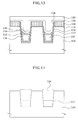
- a pad oxide layer 102 and a pad nitride layer 104 are sequentially deposited on a semiconductor substrate 100 .
- the pad oxide layer 102 reduces stresses on the semiconductor substrate 100 caused by an attracting force exerted by the pad nitride layer 104 .
- a photoresist layer is formed on the pad nitride layer 104 and is patterned to form a photoresist layer pattern 106 that selectively exposes the pad nitride layer 104 .
- An isolation layer will be formed in exposed regions of the pad nitride layer 104 to define isolation regions, and the other regions of the pad nitride layer 104 covered with the photoresist layer pattern 106 will become active regions.
- an etch process is performed using the photoresist layer pattern 106 as a mask to form trenches 112 (refer to FIG. 3 ) having a predetermined depth.
- the exposed regions of the pad nitride layer 104 are etched away using the photoresist layer pattern 106 as a mask to form a pad nitride layer pattern 108 .
- the photoresist layer pattern 106 is stripped (i.e., removed).
- the pad oxide layer 102 is etched using the pad nitride layer pattern 108 as a mask to form a pad oxide layer pattern 110 that selectively exposes the semiconductor substrate 100 .
- exposed regions of the semiconductor substrate 100 are etched away using the pad nitride layer pattern 108 and the pad oxide layer pattern 110 as masks to form the trenches 112 in the semiconductor substrate 100 to a predetermined depth (e.g., about 1600 ⁇ to about 1800 ⁇ ).
- an oxidation process is performed on the semiconductor substrate 100 to form a sidewall oxide layer 114 in the trenches 112 .
- the sidewall oxide layer 114 can be formed by thermal oxidation. Portions of the semiconductor substrate 100 can be damaged during the formation of the trenches 112 , thus the sidewall oxide layer 114 is formed to compensate for these damages.
- the sidewall oxide layer 114 prevents stresses that can be applied to the semiconductor substrate 100 by a subsequent liner nitride layer 116 . These stresses occur when the liner nitride layer 116 is directly formed on the semiconductor substrate 100 .
- the liner nitride layer 116 is deposited on the sidewall oxide layer 114 to a thickness of about 70 ⁇ to about 75 ⁇ .
- the liner nitride layer 116 prevents a leakage current caused by an oxide source permeated into the semiconductor substrate 100 during a process such as a gate oxidation process and a thermal process.
- the liner nitride layer 116 prevents a decrease in threshold voltage Vth caused by a dopant permeated into an isolation layer during an impurity implantation process for forming channels.
- a liner oxide layer 118 is formed on the liner nitride layer 116 .
- a flowable insulation layer 120 is formed above the semiconductor substrate 100 to fill the trenches 112 .
- the semiconductor substrate 100 is loaded on a spin coater.
- a compound including a solvent and a solute is applied to the semiconductor substrate 100 to form the flowable insulation layer 120 for filling the trenches 112 .
- the flowable insulation layer 120 may be a spin on dielectric (SOD) layer having good reflow characteristics.
- the flowable insulation layer 120 is formed of polysilazane.
- the flowable insulation layer 120 is treated by curing. The curing process can be performed in an H 2 or O 2 atmosphere.
- a planarization process is performed on the flowable insulation layer 120 .
- the planarization process is performed by chemical mechanical polishing (CMP) until the pad nitride layer pattern 108 is exposed. This is done so that the flowable insulation layer 120 can be uniformly recessed in a later process.
- CMP chemical mechanical polishing
- the flowable insulation layer 120 is recessed to a predetermined depth (d) to expose the liner nitride layer 116 .
- the predetermined depth (d) may range from about 1100 ⁇ to about 1400 ⁇ .
- the flowable insulation layer 120 can be recessed through a wet etch process.
- the wet etch process can be performed using a wet etch chemical such as a HF solution.
- the flowable insulation layer 120 is denoted by reference numeral 120 ′. While the flowable insulation layer 120 is recessed, the liner oxide layer 118 is etched away to the predetermined depth (d).
- the liner nitride layer 116 can be exposed to the same predetermined depth (d).
- exposed portions of the liner nitride layer 116 can be etched away.
- the thickness of the exposed portions of the liner nitride layer 116 may be reduced to a predetermined thickness, for example, about 40 ⁇ .
- an annealing process is performed on the semiconductor substrate 100 .
- the semiconductor substrate 100 is loaded in a furnace and is annealed at a temperature of about 900° C. to about 950° C. for about 20 seconds to about 30 seconds in order to densify the flowable insulation layer 120 ′.
- the trenches 112 may be fully filled through a high density plasma (HDP) process.
- HDP high density plasma
- the trenches 112 are partially filled with the flowable insulation layer 120 , and the remaining portions of the trenches 112 are filled through an HDP process.
- the flowable insulation layer 120 is recessed. While the flowable insulation layer 120 is recessed, portions of the liner nitride layer 116 exposed through the trenches 112 can increase in roughness to form rough portions 122 on lateral surfaces of the trenches 112 . For example, portions of the liner oxide layer 118 which are not etched away by an etchant such as a wet etch chemical can remain on the exposed portions of the liner nitride layer 116 to form the rough portions 122 .
- the growth rate of the buried insulation layer may be higher at lateral portions of the trenches 112 where the rough portions 122 exist than at bottom portions of the trenches 112 .
- the lateral portions of the trenches 112 can be filled before the rough portions 122 are fully filled up, thereby causing defects such as nano voids.
- a buried insulation layer 210 was formed in trenches of which lateral surfaces was rough. In this case, nano voids 200 were detected on the lateral surface of the trench.
- reference numeral 205 denotes a flowable insulation layer.
- a conductive material of the landing plug 235 can permeate into the nano voids 200 , and thus the landing plug 235 can be connected to a conductive layer 220 of the gate (a bridge defect) as indicated by portion 240 in FIG. 17 . Therefore, it is necessary to uniformly level the rough portions 122 formed on the lateral surfaces of the trenches 112 to prevent the bridge defect.
- reference numerals 215 , 225 , and 230 denote a gate insulation layer, a metal layer, and a hard mask layer, respectively.
- the semiconductor substrate 100 is treated through first and second preheating processes to reduce stresses in the sidewall oxide layer 114 and the liner nitride layer 116 .
- the semiconductor substrate 100 is loaded on a stage 305 of a high density plasma (HDP) chamber 300 shown in FIG. 15 for performing a HDP process.
- HDP high density plasma
- predetermined power is supplied to the HDP chamber 300 to perform a first preheating process for about 50 seconds to about 55 seconds.
- stresses of the sidewall oxide layer 114 and the liner nitride layer 116 can be reduced.
- the argon (Ar) gas may be supplied to the HDP chamber 300 at a flow rate of about 60 sccm to 75 sccm.
- the helium (He) gas may be supplied to the HDP chamber 300 from lateral sides 320 at a flow rate of about 250 sccm to 350 sccm, and from a topside 315 at a flow rate of about 250 sccm to 350 sccm. Further, power ranging from about 4500 W to about 5500 W may be supplied to the HDP chamber 300 from the topside 315 , and power ranging from 3500 W to 4500 W may be supplied to the HDP chamber 300 from the lateral sides 320 to generate plasma. No power is supplied to the HDP chamber 300 from a bottom side 325 .
- a second preheating process is performed by supplying preheating gases including oxygen (O 2 ) to the semiconductor substrate 100 so as to prevent the liner nitride layer 116 from being damaged by oxidation.
- the second preheating process can be performed by injecting oxygen (O 2 ), argon (Ar), and Helium (He) gases into the HDP chamber 300 and supplying a predetermined power to the HDP chamber 300 for about five seconds to about ten seconds.
- the oxygen (O 2 ) gas can be injected to the HDP chamber 300 at a flow rate of about 50 sccm to about 150 sccm, and an inert gas including the argon (Ar) gas can be injected to the HDP chamber 300 at a flow rate of about 40 sccm to about 50 sccm.
- the helium (He) gas may be injected into the HDP chamber 300 together with the oxygen (O 2 ) gas and the argon (Ar) gas.
- the helium (He) gas may be injected at a flow rate of about 200 sccm to about 300 sccm.
- Power may be supplied to the HDP chamber 300 from the topside 315 in a range from about 4500 W to about 5500 W, and power may be supplied to the HDP chamber 300 from the lateral sides 320 in a range from about 3500 W to about 4500 W. No power is supplied to the HDP chamber 300 from the bottom side 325 .
- the first and second preheating processes may be performed for no more than sixty seconds. Stresses in the liner nitride layer 116 can be released during the first and second preheating processes, and thus the liner nitride layer 116 can be prevented from lifting from the trenches 112 .
- a first buffer layer 124 is formed on the flowable insulation layer 120 ′ and the rough portions 122 formed on the side surfaces of the trenches 112 .
- a deposition source including oxygen (O 2 ), silane (SiH 4 ), and helium (He) gases is supplied to the HDP chamber 300 .
- the oxygen (O 2 ) may be supplied to the HDP chamber 300 at a flow rate of about 100 sccm to about 115 sccm.
- the silane (SiH 4 ) gas may be supplied to the HDP chamber 300 from the lateral sides 320 at a flow rate of about 40 sccm to about 55 sccm and from the topside 315 at a flow rate of about 25 sccm to about 35 sccm.
- the helium (He) gas may be supplied to the HDP chamber 300 from the lateral sides 320 at a flow rate of about 150 sccm to about 250 sccm and from the topside 315 at a flow rate of about 50 sccm to about 150 sccm.
- Power may be supplied to the HDP chamber 300 from the topside 315 in a range from about 7500 W to about 8500 W, and power may be supplied to the HDP chamber 300 from the lateral sides 320 in a range from about 4500 W to about 5500 W.
- power may be supplied to the HDP chamber 300 from the bottom side 325 in a range from about 450 W to about 550 W.
- the first buffer layer 124 is formed on the flowable insulation layer 120 ′ and the side surfaces of the trenches 112 where the liner nitride layer 116 is exposed.
- the first buffer layer 124 is formed to a proper thickness so as to prevent generation of voids at the side surfaces of the trenches 112 .
- the first buffer layer 124 may have a thickness in the range from about 250 ⁇ to about 350 ⁇ . Owing to the first buffer layer 124 , the rough portions 122 can be smoothened.
- an HDP deposition source is additionally supplied to the HDP chamber 300 to form a second buffer layer 126 that functions as a seed layer for a buried insulation layer.
- oxygen (O 2 ), silane (SiH 4 ), hydrogen (H 2 ), and helium (He) gases are supplied to the HDP chamber 300 .
- the oxygen (O 2 ) gas may be supplied to the HDP chamber 300 at a flow rate of about 70 sccm to about 80 sccm.
- the silane (SiH 4 ) gas may be supplied to the HDP chamber 300 from the lateral sides 320 at a flow rate of about 40 sccm to about 55 sccm and from the topside 315 at a flow rate of about 5 sccm to about 15 sccm.
- the helium (He) gas may be supplied to the HDP chamber 300 from the lateral sides 320 at a flow rate of about 250 sccm to about 350 sccm.
- the hydrogen (H 2 ) gas may be supplied to the HDP chamber 300 at a flow rate of about 100 sccm to about 150 sccm.
- Power may be supplied to the HDP chamber 300 from the topside 315 in a range from about 6500 W to about 7500 W, and power may be supplied to the HDP chamber 300 from the lateral sides 320 in a range from about 6500 W to about 7500 W.
- power may be supplied to the HDP chamber 300 from the bottom side 325 in a range from about 1500 W to about 2500 W.
- the second buffer layer 126 is formed on the first buffer layer 124 to a thickness of about 250 ⁇ to about 350 ⁇ .
- each of the first and second buffer layers 124 and 126 has a thickness of about 350 ⁇ or less, although the first buffer layer 124 has a thickness of about 350 ⁇ or more and the second buffer layer 126 has a thickness of about 700 ⁇ or more in a conventional method.
- each of the first and second buffer layers 124 and 126 may have a thickness in the range from about 250 ⁇ to 350 ⁇ .
- the second buffer layer 126 can be completely formed before nano voids are generated from the rough portions 122 formed on the side surfaces of the trenches 112 .
- nano voids can be generated on bottom portions of the trenches 112 .
- these nano voids on the bottom portions of the trenches 112 do not affect the characteristics of a semiconductor device.
- etch gases are supplied to the semiconductor substrate 100 to etch away the rough portions 122 from the trenches 112 .
- etch gases including nitrogen trifluoride (NF 3 ), hydrogen (H 2 ), and helium (He) gases
- a predetermined power is supplied to the HDP chamber 300 .
- the nitrogen trifluoride (NF 3 ) gas may be supplied to the HDP chamber 300 at a flow rate of about 100 sccm to about 200 sccm
- the hydrogen (H 2 ) gas may be supplied to the HDP chamber 300 at a flow rate of about 100 sccm to about 200 sccm
- the helium (He) gas may be supplied to the HDP chamber 300 at a flow rate of about 55 sccm to about 65 sccm.
- An additional amount of helium (He) gas can be supplied to the HDP chamber 300 from the topside 315 at a flow rate of about 55 sccm to about 65 sccm.
- power may be supplied to the HDP chamber 300 from the topside 315 in a range from about 1500 W to about 2500 W, and power may be supplied to the HDP chamber 300 from the lateral sides 320 in a range from about 5500 W to about 6500 W.
- power may be supplied to the HDP chamber 300 from the bottom side 325 in a range from about 1000 W to about 1800 W.
- the etch process is performed in a manner such that the liner nitride layer 116 can remain in the trenches 112 .
- the etch process may be targeted to remove a thickness of about 85 ⁇ to about 95 ⁇ .
- an etch target layer is determined based on a flat surface of the semiconductor substrate 100 such as a flat surface of the pad nitride layer pattern 108 or bottom surfaces of the trenches 112 .
- the thickness of the first and second layers 124 and 126 may range from about 250 ⁇ to about 350 ⁇ based on the above-mentioned flat surface of the semiconductor substrate 100 , and the thickness of the first and second buffer layers 124 and 126 is relatively smaller at the side surfaces of the trenches 112 than at the bottom surfaces of the trenches 112 .
- the etch process may be targeted to remove a thickness of about 85 ⁇ to about 95 ⁇ based on the thinness of the first and second buffer layers 124 and 126 at the bottom surfaces of the trenches 112 .
- the first and second buffer layer 124 and 126 may be removed from the side surfaces of the trenches.
- a predetermined thickness of the first and second buffer layers 124 and 126 may remain on the bottom surfaces of the trenches 112 .
- the liner nitride layer 116 is not damaged by the etch gases owing to the protection of the second buffer layer 126 .
- a deposition source including oxygen (O 2 ), silane (SiH 4 ), hydrogen (H 2 ), and helium (He) gases is supplied to the HDP chamber 300 to form a HDP oxide layer 128 in the trenches 112 .
- the oxygen (O 2 ) gas may be supplied to the HDP chamber 300 at a flow rate of about 70 sccm to about 80 sccm.
- the silane (SiH 4 ) gas may be supplied to the HDP chamber 300 from the lateral sides 320 at a flow rate of about 40 sccm to about 55 sccm and from the topside 315 at a flow rate of about 5 sccm to about 15 sccm.
- the helium (He) gas may be supplied to the HDP chamber 300 from the lateral sides 320 at a flow rate of about 250 sccm to about 350 sccm.
- the hydrogen (H 2 ) gas may be supplied to the HDP chamber 300 at a flow rate of about 100 sccm to about 150 sccm.
- Power may be supplied to the HDP chamber 300 from the topside 315 in a range from about 6500 W to about 7500 W, and power may be supplied to the HDP chamber 300 from the lateral sides 320 in a range from about 6500 W to about 7500 W.
- power may be supplied to the HDP chamber 300 from the bottom side 325 in a range from about 1500 W to about 2500 W.
- the HDP oxide layer 128 is formed in the trenches 112 to a thickness of about 450 ⁇ to about 550 ⁇ .
- the HDP oxide layer 128 can overhang at upper portions of the trenches 112 (refer to portion A in FIG. 11 ).
- etch gases are supplied to the HDP chamber 300 to etch away the overhangs A of the HDP oxide layer 128 from the upper portions of the trenches 112 .
- the etch gases supplied to the HDP chamber 300 includes nitrogen trifluoride (NF 3 ), hydrogen (H 2 ), and helium (He) gases.
- the nitrogen trifluoride (NF 3 ) gas may be supplied to the HDP chamber 300 at a flow rate of about 100 sccm to about 200 sccm
- the hydrogen (H 2 ) gas may be supplied to the HDP chamber 300 at a flow rate of about 100 sccm to about 200 sccm.
- the helium (He) gas may be supplied to the HDP chamber 300 at a flow rate of about 55 sccm to about 65 sccm.
- An additional amount of helium (He) gas can be supplied to the HDP chamber 300 from the topside 315 at a flow rate of about 55 sccm to about 65 sccm.
- power may be supplied to the HDP chamber 300 from the topside 315 in a range from about 1500 W to about 2500 W, and power may be supplied to the HDP chamber 300 from the lateral sides 320 in a range from about 5500 W to about 6500 W.
- power may be supplied to the HDP chamber 300 from the bottom side 325 in a range from about 1000 W to about 1800 W.
- This etch process may be targeted to remove a thickness of about 85 ⁇ to about 95 ⁇ of the HDP oxide layer 128 for removing the overhangs A.
- the overhangs A of the HDP oxide layer 128 which are formed at the upper portions of the trenches 112 due to deposition rate variations, can be removed through the etch process, and thus the HDP oxide layer 128 can be smoothened at the upper portions of the trenches 112 .
- the trenches 112 are filled with a buried insulation layer 130 by repeating an HDP oxide layer deposition process and an overhang etch process. That is, deposition is repeated after removing overhangs that obstruct filling of the trenches 112 in order to improve gap-fill characteristics for filling the trenches 112 .
- the HDP oxide layer deposition and the overhang etch process may be repeated five times (5 cycles) or more.
- an HDP oxide layer is formed to a thickness of about 700 ⁇ or more, a thickness of about 150 ⁇ or more of the HDP oxide layer is etched away, and the formation of the HDP oxide layer and the etching of the HDP oxide layer are repeated to form a buried insulation layer.
- the HDP oxide layer 128 is formed to a thickness of about 450 ⁇ to about 550 ⁇ , a thickness of about 85 ⁇ to about 95 ⁇ of the HDP oxide layer 128 is etched away, and the formation of the HDP oxide layer 128 and the etching of the HDP oxide layer 128 are repeated to form the buried insulation layer 130 . Therefore, nano voids can be reduced. Meanwhile, the first and second preheating processes to the etching process of the overhangs A of the HDP oxide layer 128 can be performed in-situ in the HDP chamber 300 .
- the roughness of the lateral surfaces of the trenches 112 can be reduced using the first and second buffer layers 124 and 126 . Furthermore, the thicknesses of the first and second buffer layers 124 and 126 are adjusted to completely form the second buffer layer 126 (a seed layer of the buried insulation layer 130 ) before the second buffer layer 126 makes contact with portions where nano voids can grow, and the rough portions 122 are removed from the lateral surfaces of the trenches 112 by etching to prevent generation of nano voids.
- bridge defects were inspected using an electron beam inspection (EBI) device. Referring to FIGS. 18A and 18B , although many bridge defects(B) were detected in a wafer processed by a conventional method, much fewer bridge defects were detected in a wafer processed according to the current embodiment of the invention.
- EBI electron beam inspection
- a planarization process is performed on the buried insulation layer 130 until the pad nitride layer pattern 108 is exposed, and the pad nitride layer pattern 108 and the pad oxide layer pattern 110 are removed to form a trench isolation layer 132 .
- the planarization process of the buried insulation layer 130 can be performed by chemical mechanical polishing (CMP).
- the first and second buffer layers are formed on the rough portions of the trenches that were formed when the flowable insulation layer is recessed in order to smoothen the rough portions, and then the rough portions are removed using etch gases. Therefore, generation of nano voids can be prevented when the buried insulation layer is formed.
- the semiconductor device can be prevented from being deteriorated by, for example, bridge detects caused by a conductive layer permeated into the isolation layer. Furthermore, since grow rates at the lateral and bottom surfaces of the trenches are adjusted by forming the first and second buffer layers to thin thicknesses, generation of nano voids can be effectively prevented.
- the deposition thicknesses of the first and second buffer layers are adjusted to completely form the second buffer layer (a seed layer of the buried insulation layer) before the second buffer layer makes contact with portions where nano voids can grow, and then the rough portions are removed from the lateral surfaces of the trenches by etching in order to prevent generation of nano voids.
Landscapes
- Engineering & Computer Science (AREA)
- Physics & Mathematics (AREA)
- Condensed Matter Physics & Semiconductors (AREA)
- General Physics & Mathematics (AREA)
- Manufacturing & Machinery (AREA)
- Computer Hardware Design (AREA)
- Microelectronics & Electronic Packaging (AREA)
- Power Engineering (AREA)
- Element Separation (AREA)
Priority Applications (1)
| Application Number | Priority Date | Filing Date | Title |
|---|---|---|---|
| US13/540,915 US20120270380A1 (en) | 2007-09-07 | 2012-07-03 | Method for forming isolation layer in semiconductor device |
Applications Claiming Priority (2)
| Application Number | Priority Date | Filing Date | Title |
|---|---|---|---|
| KR1020070091195A KR100894101B1 (ko) | 2007-09-07 | 2007-09-07 | 반도체 소자의 소자분리막 형성방법 |
| KR10-2007-0091195 | 2007-09-07 |
Related Child Applications (1)
| Application Number | Title | Priority Date | Filing Date |
|---|---|---|---|
| US13/540,915 Division US20120270380A1 (en) | 2007-09-07 | 2012-07-03 | Method for forming isolation layer in semiconductor device |
Publications (2)
| Publication Number | Publication Date |
|---|---|
| US20090068816A1 US20090068816A1 (en) | 2009-03-12 |
| US8211779B2 true US8211779B2 (en) | 2012-07-03 |
Family
ID=40432306
Family Applications (2)
| Application Number | Title | Priority Date | Filing Date |
|---|---|---|---|
| US11/958,381 Active 2028-07-08 US8211779B2 (en) | 2007-09-07 | 2007-12-17 | Method for forming isolation layer in semiconductor device |
| US13/540,915 Abandoned US20120270380A1 (en) | 2007-09-07 | 2012-07-03 | Method for forming isolation layer in semiconductor device |
Family Applications After (1)
| Application Number | Title | Priority Date | Filing Date |
|---|---|---|---|
| US13/540,915 Abandoned US20120270380A1 (en) | 2007-09-07 | 2012-07-03 | Method for forming isolation layer in semiconductor device |
Country Status (4)
| Country | Link |
|---|---|
| US (2) | US8211779B2 (zh) |
| KR (1) | KR100894101B1 (zh) |
| CN (1) | CN101383320B (zh) |
| TW (1) | TWI406359B (zh) |
Cited By (1)
| Publication number | Priority date | Publication date | Assignee | Title |
|---|---|---|---|---|
| US20220208965A1 (en) * | 2020-12-24 | 2022-06-30 | Samsung Electronics Co., Ltd. | Integrated circuit devices |
Families Citing this family (17)
| Publication number | Priority date | Publication date | Assignee | Title |
|---|---|---|---|---|
| KR101003494B1 (ko) * | 2008-04-10 | 2010-12-30 | 주식회사 하이닉스반도체 | 메모리 소자의 소자분리 구조 및 형성 방법 |
| KR100984859B1 (ko) * | 2008-04-29 | 2010-10-04 | 주식회사 하이닉스반도체 | 반도체 소자의 소자분리막 및 그 형성방법 |
| JP2010027904A (ja) * | 2008-07-22 | 2010-02-04 | Elpida Memory Inc | 半導体装置の製造方法 |
| US7674684B2 (en) * | 2008-07-23 | 2010-03-09 | Applied Materials, Inc. | Deposition methods for releasing stress buildup |
| KR101069438B1 (ko) * | 2009-09-14 | 2011-09-30 | 주식회사 하이닉스반도체 | 반도체 소자의 소자분리막 형성방법 |
| KR101576296B1 (ko) * | 2009-12-11 | 2015-12-10 | 주식회사 동부하이텍 | 반도체 소자용 커패시터 및 반도체 소자용 커패시터의 제조 방법 |
| US8921183B2 (en) * | 2010-12-08 | 2014-12-30 | Nanya Technology Corporation | Method for fabricating trench isolation structure |
| KR101890818B1 (ko) * | 2012-03-26 | 2018-08-22 | 에스케이하이닉스 주식회사 | 소자분리막을 구비한 반도체 장치, 이를 구비한 전자장치 및 그 제조방법 |
| US8603895B1 (en) * | 2012-09-11 | 2013-12-10 | Globalfoundries Inc. | Methods of forming isolation structures for semiconductor devices by performing a deposition-etch-deposition sequence |
| KR101617252B1 (ko) | 2012-09-21 | 2016-05-02 | 삼성전자주식회사 | 트랜지스터의 형성 방법 및 이를 포함하는 반도체 장치의 제조 방법 |
| KR101983309B1 (ko) * | 2012-10-26 | 2019-05-29 | 삼성전자주식회사 | 메모리 소자 및 이의 제조방법 |
| US9397143B2 (en) * | 2013-12-20 | 2016-07-19 | Intel Corporation | Liner for phase change memory (PCM) array and associated techniques and configurations |
| CN104835775B (zh) * | 2014-02-08 | 2018-01-30 | 中芯国际集成电路制造(上海)有限公司 | 一种浅沟道隔离结构的制备方法 |
| US9711351B2 (en) * | 2014-09-11 | 2017-07-18 | Asm Ip Holding B.V. | Process for densifying nitride film |
| TWI555179B (zh) * | 2015-02-02 | 2016-10-21 | 力晶科技股份有限公司 | 隔離結構及具有其之非揮發性記憶體的製造方法 |
| KR102606653B1 (ko) | 2017-03-31 | 2023-11-24 | 어플라이드 머티어리얼스, 인코포레이티드 | 고종횡비 트렌치들을 비정질 실리콘 막으로 갭충전하기 위한 2-단계 프로세스 |
| TWI730677B (zh) * | 2020-03-18 | 2021-06-11 | 力晶積成電子製造股份有限公司 | 記憶體元件及其製造方法 |
Citations (20)
| Publication number | Priority date | Publication date | Assignee | Title |
|---|---|---|---|---|
| KR20000003426A (ko) | 1998-06-29 | 2000-01-15 | 김영환 | 반도체 장치의 소자 분리막 형성방법 |
| US6287988B1 (en) * | 1997-03-18 | 2001-09-11 | Kabushiki Kaisha Toshiba | Semiconductor device manufacturing method, semiconductor device manufacturing apparatus and semiconductor device |
| KR20020045401A (ko) | 2000-12-08 | 2002-06-19 | 윤종용 | 트렌치 소자 분리막 형성 방법 |
| KR20020061354A (ko) | 2001-01-16 | 2002-07-24 | 삼성전자 주식회사 | 트렌치 소자 분리구조를 가지는 반도체 소자 및 트렌치소자 분리 방법 |
| US20020123206A1 (en) | 2001-03-05 | 2002-09-05 | Hong Soo-Jin | Method of forming an insulating layer in a trench isolation type semiconductor device |
| US20030013272A1 (en) * | 2001-07-03 | 2003-01-16 | Hong Soo-Jin | Trench device isolation structure and a method of forming the same |
| CN1123921C (zh) | 1999-04-16 | 2003-10-08 | 国际商业机器公司 | 高选择性颈圈氧化物腐蚀工艺 |
| US20040072408A1 (en) * | 2002-10-10 | 2004-04-15 | Yun Jae-Sun | Methods of forming trench isolated integrated circuit devices including grooves, and trench isolated integrated circuit devices so formed |
| US20040198019A1 (en) * | 2003-04-02 | 2004-10-07 | Renesas Technology Corp. | Manufacturing method of semiconductor device |
| KR20050002317A (ko) | 2003-06-30 | 2005-01-07 | 주식회사 하이닉스반도체 | 반도체 소자의 제조 방법 |
| US20050009293A1 (en) | 2003-07-10 | 2005-01-13 | Samsung Electronics Co., Ltd | Method of forming trench isolations |
| US20050139938A1 (en) * | 2003-12-27 | 2005-06-30 | Dongbuanam Semiconductor Inc. | Semiconductor device and method of manufacturing the same |
| US20050167778A1 (en) * | 2004-02-03 | 2005-08-04 | Shin-Hye Kim | Shallow trench isolation structure with converted liner layer |
| KR20050118489A (ko) | 2004-06-14 | 2005-12-19 | 주식회사 하이닉스반도체 | 반도체 소자의 소자분리 방법 |
| US20060038254A1 (en) | 2004-08-23 | 2006-02-23 | Joohyun Jin | Trench isolation structure and method of formation |
| US20060068562A1 (en) | 2004-09-29 | 2006-03-30 | Agere Systems Inc. | Trench isolation structure and method of manufacture therefor |
| KR20060070364A (ko) | 2004-12-20 | 2006-06-23 | 주식회사 하이닉스반도체 | 소자 분리막 형성 방법 |
| US20060270183A1 (en) | 2005-05-27 | 2006-11-30 | Samsung Electronics Co., Ltd. | Isolation structure and method of forming the same |
| US20070020877A1 (en) | 2005-07-21 | 2007-01-25 | Taiwan Semiconductor Manufacturing Co., Ltd. | Shallow trench isolation structure and method of fabricating the same |
| US20070173015A1 (en) * | 2006-01-23 | 2007-07-26 | Hynix Semiconductor Inc. | Method for Fabricating Semiconductor Device |
Family Cites Families (6)
| Publication number | Priority date | Publication date | Assignee | Title |
|---|---|---|---|---|
| US6380056B1 (en) * | 1998-10-23 | 2002-04-30 | Taiwan Semiconductor Manufacturing Company | Lightly nitridation surface for preparing thin-gate oxides |
| US7000175B2 (en) * | 2000-11-03 | 2006-02-14 | Agere Systems Inc. | Method and apparatus for pipelined joint equalization and decoding for gigabit communications |
| US7095460B2 (en) * | 2001-02-26 | 2006-08-22 | Samsung Electronics Co., Ltd. | Thin film transistor array substrate using low dielectric insulating layer and method of fabricating the same |
| US7118987B2 (en) * | 2004-01-29 | 2006-10-10 | Taiwan Semiconductor Manufacturing Co., Ltd. | Method of achieving improved STI gap fill with reduced stress |
| KR100653994B1 (ko) * | 2005-03-14 | 2006-12-05 | 주식회사 하이닉스반도체 | 반도체 소자의 층간절연막 형성방법 |
| US7482244B2 (en) * | 2005-09-16 | 2009-01-27 | United Microelectronics Corp. | Method of preventing a peeling issue of a high stressed thin film |
-
2007
- 2007-09-07 KR KR1020070091195A patent/KR100894101B1/ko not_active IP Right Cessation
- 2007-12-17 US US11/958,381 patent/US8211779B2/en active Active
-
2008
- 2008-02-25 TW TW097106434A patent/TWI406359B/zh not_active IP Right Cessation
- 2008-05-05 CN CN2008100953736A patent/CN101383320B/zh not_active Expired - Fee Related
-
2012
- 2012-07-03 US US13/540,915 patent/US20120270380A1/en not_active Abandoned
Patent Citations (20)
| Publication number | Priority date | Publication date | Assignee | Title |
|---|---|---|---|---|
| US6287988B1 (en) * | 1997-03-18 | 2001-09-11 | Kabushiki Kaisha Toshiba | Semiconductor device manufacturing method, semiconductor device manufacturing apparatus and semiconductor device |
| KR20000003426A (ko) | 1998-06-29 | 2000-01-15 | 김영환 | 반도체 장치의 소자 분리막 형성방법 |
| CN1123921C (zh) | 1999-04-16 | 2003-10-08 | 国际商业机器公司 | 高选择性颈圈氧化物腐蚀工艺 |
| KR20020045401A (ko) | 2000-12-08 | 2002-06-19 | 윤종용 | 트렌치 소자 분리막 형성 방법 |
| KR20020061354A (ko) | 2001-01-16 | 2002-07-24 | 삼성전자 주식회사 | 트렌치 소자 분리구조를 가지는 반도체 소자 및 트렌치소자 분리 방법 |
| US20020123206A1 (en) | 2001-03-05 | 2002-09-05 | Hong Soo-Jin | Method of forming an insulating layer in a trench isolation type semiconductor device |
| US20030013272A1 (en) * | 2001-07-03 | 2003-01-16 | Hong Soo-Jin | Trench device isolation structure and a method of forming the same |
| US20040072408A1 (en) * | 2002-10-10 | 2004-04-15 | Yun Jae-Sun | Methods of forming trench isolated integrated circuit devices including grooves, and trench isolated integrated circuit devices so formed |
| US20040198019A1 (en) * | 2003-04-02 | 2004-10-07 | Renesas Technology Corp. | Manufacturing method of semiconductor device |
| KR20050002317A (ko) | 2003-06-30 | 2005-01-07 | 주식회사 하이닉스반도체 | 반도체 소자의 제조 방법 |
| US20050009293A1 (en) | 2003-07-10 | 2005-01-13 | Samsung Electronics Co., Ltd | Method of forming trench isolations |
| US20050139938A1 (en) * | 2003-12-27 | 2005-06-30 | Dongbuanam Semiconductor Inc. | Semiconductor device and method of manufacturing the same |
| US20050167778A1 (en) * | 2004-02-03 | 2005-08-04 | Shin-Hye Kim | Shallow trench isolation structure with converted liner layer |
| KR20050118489A (ko) | 2004-06-14 | 2005-12-19 | 주식회사 하이닉스반도체 | 반도체 소자의 소자분리 방법 |
| US20060038254A1 (en) | 2004-08-23 | 2006-02-23 | Joohyun Jin | Trench isolation structure and method of formation |
| US20060068562A1 (en) | 2004-09-29 | 2006-03-30 | Agere Systems Inc. | Trench isolation structure and method of manufacture therefor |
| KR20060070364A (ko) | 2004-12-20 | 2006-06-23 | 주식회사 하이닉스반도체 | 소자 분리막 형성 방법 |
| US20060270183A1 (en) | 2005-05-27 | 2006-11-30 | Samsung Electronics Co., Ltd. | Isolation structure and method of forming the same |
| US20070020877A1 (en) | 2005-07-21 | 2007-01-25 | Taiwan Semiconductor Manufacturing Co., Ltd. | Shallow trench isolation structure and method of fabricating the same |
| US20070173015A1 (en) * | 2006-01-23 | 2007-07-26 | Hynix Semiconductor Inc. | Method for Fabricating Semiconductor Device |
Cited By (2)
| Publication number | Priority date | Publication date | Assignee | Title |
|---|---|---|---|---|
| US20220208965A1 (en) * | 2020-12-24 | 2022-06-30 | Samsung Electronics Co., Ltd. | Integrated circuit devices |
| US11670676B2 (en) * | 2020-12-24 | 2023-06-06 | Samsung Electronics Co., Ltd. | Integrated circuit devices |
Also Published As
| Publication number | Publication date |
|---|---|
| CN101383320A (zh) | 2009-03-11 |
| TW200913127A (en) | 2009-03-16 |
| TWI406359B (zh) | 2013-08-21 |
| US20090068816A1 (en) | 2009-03-12 |
| CN101383320B (zh) | 2011-04-06 |
| KR20090025961A (ko) | 2009-03-11 |
| KR100894101B1 (ko) | 2009-04-20 |
| US20120270380A1 (en) | 2012-10-25 |
Similar Documents
| Publication | Publication Date | Title |
|---|---|---|
| US8211779B2 (en) | Method for forming isolation layer in semiconductor device | |
| US8003489B2 (en) | Method for forming isolation layer in semiconductor device | |
| KR101003494B1 (ko) | 메모리 소자의 소자분리 구조 및 형성 방법 | |
| US7902037B2 (en) | Isolation structure in memory device and method for fabricating the same | |
| KR100818711B1 (ko) | 반도체 소자의 소자분리막 형성방법 | |
| US20090004839A1 (en) | Method for fabricating an interlayer dielectric in a semiconductor device | |
| JP2002110782A (ja) | 半導体装置およびその製造方法 | |
| US6737328B1 (en) | Methods of forming silicon dioxide layers, and methods of forming trench isolation regions | |
| KR100914293B1 (ko) | 반도체소자의 트렌치 소자분리막 형성방법 | |
| KR20060122139A (ko) | 플래쉬 메모리 소자의 제조방법 | |
| KR100842749B1 (ko) | 반도체소자의 트렌치 소자분리막 형성방법 | |
| US20050112841A1 (en) | Method for isolating semiconductor devices | |
| KR100869852B1 (ko) | 반도체 소자의 소자분리막 형성방법 | |
| KR20080002613A (ko) | 반도체 소자의 소자분리 형성방법 | |
| KR20020010971A (ko) | 반도체소자의 소자분리막 형성 방법 | |
| KR100831682B1 (ko) | 반도체 소자의 소자분리막 형성방법 | |
| KR100884347B1 (ko) | 반도체 소자의 소자분리막 형성방법 | |
| KR101168637B1 (ko) | 반도체 소자의 절연막 형성방법 | |
| KR100842901B1 (ko) | 반도체 소자의 소자분리막 형성방법 | |
| KR100849073B1 (ko) | 반도체 소자의 소자분리막 형성방법 | |
| KR20120042045A (ko) | 반도체 소자의 제조 방법 | |
| KR19990004577A (ko) | 반도체소자의 소자분리절연막 형성방법 | |
| KR20050011190A (ko) | 저온 플라즈마 산화막을 이용한 반도체 소자의 소자분리막형성방법 | |
| KR20020018875A (ko) | 반도체장치의 sti형 소자분리막 형성방법 | |
| KR20040059439A (ko) | 반도체 소자의 트렌치형 소자분리막 형성방법 |
Legal Events
| Date | Code | Title | Description |
|---|---|---|---|
| AS | Assignment |
Owner name: HYNIX SEMICONDUCTOR INC., KOREA, REPUBLIC OF Free format text: ASSIGNMENT OF ASSIGNORS INTEREST;ASSIGNOR:EUN, BYUNG SOO;REEL/FRAME:020469/0070 Effective date: 20071123 |
|
| STCF | Information on status: patent grant |
Free format text: PATENTED CASE |
|
| FEPP | Fee payment procedure |
Free format text: PAYOR NUMBER ASSIGNED (ORIGINAL EVENT CODE: ASPN); ENTITY STATUS OF PATENT OWNER: LARGE ENTITY |
|
| FPAY | Fee payment |
Year of fee payment: 4 |
|
| MAFP | Maintenance fee payment |
Free format text: PAYMENT OF MAINTENANCE FEE, 8TH YEAR, LARGE ENTITY (ORIGINAL EVENT CODE: M1552); ENTITY STATUS OF PATENT OWNER: LARGE ENTITY Year of fee payment: 8 |
|
| FEPP | Fee payment procedure |
Free format text: MAINTENANCE FEE REMINDER MAILED (ORIGINAL EVENT CODE: REM.); ENTITY STATUS OF PATENT OWNER: LARGE ENTITY |