US7800165B2 - Semiconductor device and method for producing the same - Google Patents
Semiconductor device and method for producing the same Download PDFInfo
- Publication number
- US7800165B2 US7800165B2 US12/025,504 US2550408A US7800165B2 US 7800165 B2 US7800165 B2 US 7800165B2 US 2550408 A US2550408 A US 2550408A US 7800165 B2 US7800165 B2 US 7800165B2
- Authority
- US
- United States
- Prior art keywords
- region
- impurity region
- semiconductor
- impurity
- condition
- Prior art date
- Legal status (The legal status is an assumption and is not a legal conclusion. Google has not performed a legal analysis and makes no representation as to the accuracy of the status listed.)
- Active, expires
Links
- 239000004065 semiconductor Substances 0.000 title claims abstract description 385
- 238000004519 manufacturing process Methods 0.000 title description 34
- 239000012535 impurity Substances 0.000 claims abstract description 352
- 239000000758 substrate Substances 0.000 claims abstract description 62
- 230000007480 spreading Effects 0.000 claims description 27
- 238000003892 spreading Methods 0.000 claims description 27
- 125000006850 spacer group Chemical group 0.000 claims description 18
- 238000002513 implantation Methods 0.000 description 78
- 239000007789 gas Substances 0.000 description 63
- 238000000034 method Methods 0.000 description 44
- 150000002500 ions Chemical class 0.000 description 34
- 238000004544 sputter deposition Methods 0.000 description 26
- 239000000463 material Substances 0.000 description 22
- 230000007423 decrease Effects 0.000 description 18
- VYPSYNLAJGMNEJ-UHFFFAOYSA-N Silicium dioxide Chemical compound O=[Si]=O VYPSYNLAJGMNEJ-UHFFFAOYSA-N 0.000 description 12
- XUIMIQQOPSSXEZ-UHFFFAOYSA-N Silicon Chemical compound [Si] XUIMIQQOPSSXEZ-UHFFFAOYSA-N 0.000 description 12
- 229910052710 silicon Inorganic materials 0.000 description 12
- 239000010703 silicon Substances 0.000 description 12
- ZOXJGFHDIHLPTG-UHFFFAOYSA-N Boron Chemical group [B] ZOXJGFHDIHLPTG-UHFFFAOYSA-N 0.000 description 10
- 230000008569 process Effects 0.000 description 10
- 230000015572 biosynthetic process Effects 0.000 description 8
- 230000008859 change Effects 0.000 description 8
- 238000007796 conventional method Methods 0.000 description 8
- 230000000694 effects Effects 0.000 description 8
- 238000003795 desorption Methods 0.000 description 7
- 230000007246 mechanism Effects 0.000 description 7
- 229910052796 boron Inorganic materials 0.000 description 6
- 230000007935 neutral effect Effects 0.000 description 6
- 239000000523 sample Substances 0.000 description 5
- 229910052814 silicon oxide Inorganic materials 0.000 description 5
- 238000000137 annealing Methods 0.000 description 4
- 230000015556 catabolic process Effects 0.000 description 4
- 238000006731 degradation reaction Methods 0.000 description 4
- 230000005669 field effect Effects 0.000 description 4
- 229910021420 polycrystalline silicon Inorganic materials 0.000 description 4
- 229920005591 polysilicon Polymers 0.000 description 4
- 230000003247 decreasing effect Effects 0.000 description 3
- 238000010438 heat treatment Methods 0.000 description 3
- 238000005468 ion implantation Methods 0.000 description 3
- 238000005259 measurement Methods 0.000 description 3
- 230000003213 activating effect Effects 0.000 description 2
- 230000001419 dependent effect Effects 0.000 description 2
- 238000007865 diluting Methods 0.000 description 2
- 238000001312 dry etching Methods 0.000 description 2
- 239000001307 helium Substances 0.000 description 2
- 229910052734 helium Inorganic materials 0.000 description 2
- SWQJXJOGLNCZEY-UHFFFAOYSA-N helium atom Chemical compound [He] SWQJXJOGLNCZEY-UHFFFAOYSA-N 0.000 description 2
- 125000004435 hydrogen atom Chemical group [H]* 0.000 description 2
- 239000012212 insulator Substances 0.000 description 2
- 230000010354 integration Effects 0.000 description 2
- 125000001319 lambda(5)-arsanyl group Chemical group [H][As]([H])([H])([H])[*] 0.000 description 2
- 238000004151 rapid thermal annealing Methods 0.000 description 2
- 230000009467 reduction Effects 0.000 description 2
- 238000001179 sorption measurement Methods 0.000 description 2
- 238000005406 washing Methods 0.000 description 2
- XYFCBTPGUUZFHI-UHFFFAOYSA-N Phosphine Chemical compound P XYFCBTPGUUZFHI-UHFFFAOYSA-N 0.000 description 1
- 230000009471 action Effects 0.000 description 1
- 230000004913 activation Effects 0.000 description 1
- 125000004429 atom Chemical group 0.000 description 1
- 230000004888 barrier function Effects 0.000 description 1
- 239000000470 constituent Substances 0.000 description 1
- 238000000354 decomposition reaction Methods 0.000 description 1
- 238000005516 engineering process Methods 0.000 description 1
- -1 for example Substances 0.000 description 1
- 239000002184 metal Substances 0.000 description 1
- 230000007704 transition Effects 0.000 description 1
Images


Classifications
-
- H—ELECTRICITY
- H01—ELECTRIC ELEMENTS
- H01L—SEMICONDUCTOR DEVICES NOT COVERED BY CLASS H10
- H01L29/00—Semiconductor devices adapted for rectifying, amplifying, oscillating or switching, or capacitors or resistors with at least one potential-jump barrier or surface barrier, e.g. PN junction depletion layer or carrier concentration layer; Details of semiconductor bodies or of electrodes thereof ; Multistep manufacturing processes therefor
- H01L29/66—Types of semiconductor device ; Multistep manufacturing processes therefor
- H01L29/68—Types of semiconductor device ; Multistep manufacturing processes therefor controllable by only the electric current supplied, or only the electric potential applied, to an electrode which does not carry the current to be rectified, amplified or switched
- H01L29/76—Unipolar devices, e.g. field effect transistors
- H01L29/772—Field effect transistors
- H01L29/78—Field effect transistors with field effect produced by an insulated gate
- H01L29/785—Field effect transistors with field effect produced by an insulated gate having a channel with a horizontal current flow in a vertical sidewall of a semiconductor body, e.g. FinFET, MuGFET
-
- H—ELECTRICITY
- H01—ELECTRIC ELEMENTS
- H01L—SEMICONDUCTOR DEVICES NOT COVERED BY CLASS H10
- H01L29/00—Semiconductor devices adapted for rectifying, amplifying, oscillating or switching, or capacitors or resistors with at least one potential-jump barrier or surface barrier, e.g. PN junction depletion layer or carrier concentration layer; Details of semiconductor bodies or of electrodes thereof ; Multistep manufacturing processes therefor
- H01L29/66—Types of semiconductor device ; Multistep manufacturing processes therefor
- H01L29/66007—Multistep manufacturing processes
- H01L29/66075—Multistep manufacturing processes of devices having semiconductor bodies comprising group 14 or group 13/15 materials
- H01L29/66227—Multistep manufacturing processes of devices having semiconductor bodies comprising group 14 or group 13/15 materials the devices being controllable only by the electric current supplied or the electric potential applied, to an electrode which does not carry the current to be rectified, amplified or switched, e.g. three-terminal devices
- H01L29/66409—Unipolar field-effect transistors
- H01L29/66477—Unipolar field-effect transistors with an insulated gate, i.e. MISFET
- H01L29/66787—Unipolar field-effect transistors with an insulated gate, i.e. MISFET with a gate at the side of the channel
- H01L29/66795—Unipolar field-effect transistors with an insulated gate, i.e. MISFET with a gate at the side of the channel with a horizontal current flow in a vertical sidewall of a semiconductor body, e.g. FinFET, MuGFET
- H01L29/66803—Unipolar field-effect transistors with an insulated gate, i.e. MISFET with a gate at the side of the channel with a horizontal current flow in a vertical sidewall of a semiconductor body, e.g. FinFET, MuGFET with a step of doping the vertical sidewall, e.g. using tilted or multi-angled implants
-
- H—ELECTRICITY
- H01—ELECTRIC ELEMENTS
- H01L—SEMICONDUCTOR DEVICES NOT COVERED BY CLASS H10
- H01L29/00—Semiconductor devices adapted for rectifying, amplifying, oscillating or switching, or capacitors or resistors with at least one potential-jump barrier or surface barrier, e.g. PN junction depletion layer or carrier concentration layer; Details of semiconductor bodies or of electrodes thereof ; Multistep manufacturing processes therefor
- H01L29/66—Types of semiconductor device ; Multistep manufacturing processes therefor
- H01L29/68—Types of semiconductor device ; Multistep manufacturing processes therefor controllable by only the electric current supplied, or only the electric potential applied, to an electrode which does not carry the current to be rectified, amplified or switched
- H01L29/76—Unipolar devices, e.g. field effect transistors
- H01L29/772—Field effect transistors
- H01L29/78—Field effect transistors with field effect produced by an insulated gate
- H01L29/786—Thin film transistors, i.e. transistors with a channel being at least partly a thin film
- H01L29/78606—Thin film transistors, i.e. transistors with a channel being at least partly a thin film with supplementary region or layer in the thin film or in the insulated bulk substrate supporting it for controlling or increasing the safety of the device
- H01L29/78618—Thin film transistors, i.e. transistors with a channel being at least partly a thin film with supplementary region or layer in the thin film or in the insulated bulk substrate supporting it for controlling or increasing the safety of the device characterised by the drain or the source properties, e.g. the doping structure, the composition, the sectional shape or the contact structure
- H01L29/78621—Thin film transistors, i.e. transistors with a channel being at least partly a thin film with supplementary region or layer in the thin film or in the insulated bulk substrate supporting it for controlling or increasing the safety of the device characterised by the drain or the source properties, e.g. the doping structure, the composition, the sectional shape or the contact structure with LDD structure or an extension or an offset region or characterised by the doping profile
Definitions
- the present invention relates to a semiconductor device and a method for producing the same, and more particularly to a semiconductor device of a three-dimensional structure including fin-shaped semiconductor regions on a substrate and a method for producing the same.
- a field effect transistors having the fin-shaped structure is commonly called a fin-shaped FET (field effect transistor), and has an active region including thin wall (fin)-like semiconductor regions perpendicular to the principle plane of the substrate.
- fin-shaped FET field effect transistor
- the side surface of the semiconductor region can be used as a channel surface, whereby it is possible to reduce the area on the substrate taken up by the transistor (see, for example, Patent Document 1 and Non-Patent Document 1).
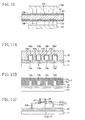
- FIG. 16A to FIG. 16D show a structure of a conventional fin-shaped FET, wherein FIG. 16A is a plan view of the device, FIG. 16B is a cross-sectional view taken along line A-A in FIG. 16A , FIG. 16C is a cross-sectional view taken along line B-B in FIG. 16A , and FIG. 16D is a cross-sectional view taken along line C-C in FIG. 16 A.
- a conventional fin-shaped FET includes a supporting substrate 101 made of silicon, an insulating layer 102 made of silicon oxide formed on the supporting substrate 101 , semiconductor regions 103 a to 103 d each formed into a fin shape on the insulating layer 102 (hereinafter referred to as the “fin-shaped semiconductor regions”), a gate electrode 105 formed on the fin-shaped semiconductor regions 103 a to 103 d via gate insulating films 104 a to 104 d , insulative sidewall spacers 106 formed on side surfaces of the gate electrode 105 , extension regions 107 formed on opposite side regions of the fin-shaped semiconductor regions 103 a to 103 d sandwiching the gate electrode 105 therebetween, and source-drain regions 117 formed on opposite side regions of the fin-shaped semiconductor regions 103 a to 103 d sandwiching the gate electrode 105 and the insulative sidewall spacer 106 therebetween.
- the fin-shaped semiconductor regions 103 a to 103 d are placed on the insulating layer 102 so as to be arranged at regular intervals in the gate width direction.
- the gate electrode 105 is formed so as to extend across the fin-shaped semiconductor regions 103 a to 103 d in the gate width direction.
- the extension region 107 includes a first impurity region 107 a formed in an upper portion of each of the fin-shaped semiconductor regions 103 a to 103 d , and a second impurity region 107 b formed in a side portion of each of the fin-shaped semiconductor regions 103 a to 103 d .
- the source-drain region 117 includes a third impurity region 117 a formed in an upper portion of each of the fin-shaped semiconductor regions 103 a to 103 d , and a fourth impurity region 117 b formed in a side portion of each of the fin-shaped semiconductor regions 103 a to 103 d . Note that pocket regions are not described herein or shown in the figure.
- FIG. 17A to FIG. 17D are cross-sectional views, showing, step by step, a conventional method for producing a semiconductor device. Note that FIG. 17A to FIG. 17D correspond to the cross-sectional structure taken along line C-C in FIG. 16A . In FIG. 17A to FIG. 17D , like elements to those shown in FIG. 16A to FIG. 16D are denoted by like reference numerals and will not be described again.
- an SOI (silicon on insulator) substrate in which the insulating layer 102 made of silicon oxide is provided on the supporting substrate 101 made of silicon, and a semiconductor layer made of silicon is provided on the insulating layer 102 . Then, the semiconductor layer is patterned to form the fin-shaped semiconductor region 103 b to be the active region.
- SOI silicon on insulator
- the gate insulating film 104 is formed on the surface of the fin-shaped semiconductor region 103 b , after which a polysilicon film 105 A is formed across the entire surface of the supporting substrate 102 .
- the polysilicon film 105 A and the gate insulating film 104 are etched successively to form the gate electrode 105 on the fin-shaped semiconductor region 103 b with the gate insulating film 104 b interposed therebetween.
- the semiconductor region 103 b is ion-implanted with an impurity to form the extension region 107 and the pocket region (not shown).
- an insulating film is formed across the entire surface of the supporting substrate 102 , and then the insulating film is etched back by using anisotropic dry etching to thereby form the insulative sidewall spacer 106 on the side surface of the gate electrode 105 . Then, using the gate electrode 105 and the side wall 106 as a mask, the semiconductor region 103 b is ion-implanted with an impurity to form the source-drain region 117 .
- Patent Document 1 Japanese Laid-Open Patent Publication No. 2006-196821
- Non-Patent Document 1 D. Lenoble, et al., Enhanced performance of PMOS MUGFET via integration of conformal plasma-doped source/drain extensions, 2006 Symposium on VLSI Technology Digest of Technical Papers, p. 212
- the present inventors have studied the reason why desirable transistor characteristics cannot be obtained with the conventional methods for producing a fin-shaped FET, which lead to the following findings.
- FIG. 18A is a cross-sectional view of an important part showing the step of forming an extension region of a fin-shaped FET as described in Patent Document 1
- FIG. 18B is a cross-sectional view showing the step of forming an extension region of a fin-shaped FET as described in Non-Patent Document 1.
- FIG. 18A and FIG. 18B correspond to the cross-sectional structure (before the formation of the insulative sidewall spacer 106 ) taken along line B-B in FIG. 16A .
- like elements to those shown in FIG. 16A to FIG. 16D are denoted by like reference numerals.
- ions 108 a and 108 b are implanted by ion implantation into the fin-shaped semiconductor regions 103 a to 103 d at respective implantation angles inclined with respect to the vertical direction in different directions from each other, thus forming the extension region 107 .
- the first impurity region 107 a into which the ions 108 a and the ions 108 b are both implanted, is formed in the upper portion of the fin-shaped semiconductor regions 103 a to 103 d .
- the second impurity region 107 b into which either the ions 108 a or the ions 108 b are implanted, is formed in each side portion of the fin-shaped semiconductor regions 103 a to 103 d .
- the implantation dose of the first impurity region 107 a is twice as large as the implantation dose of the second impurity region 107 b.
- the extension region 107 is formed in the fin-shaped semiconductor regions 103 a to 103 d by using a plasma doping method.
- the first impurity region 107 a is formed in an upper portion of the fin-shaped semiconductor regions 103 a to 103 d , wherein the implantation dose of the first impurity region 107 a is dictated by the balance between implanted ions 109 a , an adsorbed species (a neutral species such as gas molecules or radicals) 109 b , and an impurity 109 c that is desorbed from the fin-shaped semiconductor regions 103 a to 103 d by sputtering.
- an adsorbed species a neutral species such as gas molecules or radicals
- the implantation dose of each side portion of the fin-shaped semiconductor regions 103 a to 103 d is less influenced by the implanted ions 109 a and the impurity 109 c desorbed by sputtering, and there is formed the second impurity region 107 b whose implantation dose is mainly dictated by the adsorbed species 109 b .
- the implantation dose of the first impurity region 107 a is higher than that of the second impurity region 107 b by about 25%, for example.
- the implantation dose of the first impurity region 107 a formed in an upper portion of the fin-shaped semiconductor regions 103 a to 103 d is higher than that of the second impurity region 107 b formed in a side portion of the fin-shaped semiconductor regions 103 a to 103 d .
- the junction depth of the second impurity region 107 b is shallower than that of the first impurity region 107 a . Accordingly, the sheet resistance, the resistivity, or the spreading resistance of the first impurity region 107 a is lower than the sheet resistance, the resistivity, or the spreading resistance of the second impurity region 107 b .
- ⁇ w CF ⁇ k ⁇ /2 ⁇ r, which is widely known in the art of spreading resistance measurement, proportion of Rs to ⁇ w/t is lead (i.e., main component) since the specific resistance (resistivity) ⁇ and the spreading resistance ⁇ w are basically in one to one correspondence.
- CF is a correction factor with the volume effect of the spreading resistance ⁇ w taken into consideration (wherein, with no correction, CF is 1)
- k is a correction factor with the polarity dependency in Schottky barrier between a probe and a sample taken into consideration (for example, k is 1 when a sample is made of p-type silicon, or k is any of 1 to 3 when a sample is made of n-type silicon)
- r is a radius of curvature of the tip end of a probe.
- the current flowing through the extension region 107 is localized in the first impurity region 107 a where the implantation dose is higher, i.e., the sheet resistance is lower, than the second impurity region 107 b , thereby failing to obtain desirable transistor characteristics.
- the source-drain region is also formed by using an ion implantation method or a plasma doping method similar to that for the extension region. Therefore, also in the source-drain region 117 , the implantation dose of the third impurity region 117 a formed in an upper portion of the fin-shaped semiconductor regions 103 a to 103 d is higher than that of the fourth impurity region 117 b formed in a side portion of the fin-shaped semiconductor regions 103 a to 103 d . Moreover, the junction depth of the fourth impurity region 117 b is shallower than that of the third impurity region 117 a .
- the current flowing through the source-drain region 117 is localized in the third impurity region 117 a where the implantation dose is higher, i.e., the sheet resistance is lower, than the fourth impurity region 117 b , thereby failing to obtain desirable transistor characteristics.
- the present inventors have invented a semiconductor device including an impurity region in a side portion of a fin-shaped semiconductor region where the implantation dose is substantially equal to or greater than that in an upper portion of the fin-shaped semiconductor region, and a method for producing the same.
- the width of the impurity region formed in a side portion of the fin-shaped semiconductor region accounts for 70% or more of the width of the extension region and the source-drain region in the gate width direction. Therefore, it has become important that the implantation dose of the impurity region formed in a side portion of the fin-shaped semiconductor region is made substantially equal to or greater than that of the impurity region formed in an upper portion of the fin-shaped semiconductor region.
- the resistivity, the spreading resistance, or the sheet resistance of the impurity region formed in the side portion of the fin-shaped semiconductor region it is important to set the resistivity, the spreading resistance, or the sheet resistance of the impurity region formed in the side portion of the fin-shaped semiconductor region to be equal to or smaller than the resistivity, the spreading resistance, or the sheet resistance of the impurity region formed in the upper portion of the fin-shaped semiconductor region.
- a first semiconductor device of the present invention is a semiconductor device, including: a first semiconductor region formed on a supporting substrate and having an upper surface and a side surface; a first impurity region of a first conductivity type formed in an upper portion of the first semiconductor region; and a second impurity region of a first conductivity type formed in a side portion of the first semiconductor region, wherein a resistivity of the second impurity region is substantially equal to or smaller than that of the first impurity region.
- the transistor characteristics can be significantly improved over the conventional techniques if the implantation dose of the second impurity region formed in a side portion of the first semiconductor region having an upper surface and a side surface, i.e., the fin-shaped semiconductor region, is about 80% (more preferably 90%) or more of that of the first impurity region formed in an upper portion of the fin-shaped semiconductor region.
- the aspect ratio the height of the side surface of the fin-shaped semiconductor region”/“the width of the upper surface of the fin-shaped semiconductor region in the gate width direction” (hereinafter referred to as the “aspect ratio”) is small, there will be little degradation in the transistor characteristics even if the implantation dose of the second impurity region is somewhat smaller than that of the first impurity region.
- An increase in the aspect ratio accordingly increases the necessity to make the implantation dose of the second impurity region to be substantially equal to or greater than that of the first impurity region.
- the junction depth of the second impurity region may be substantially equal to or greater than that of the first impurity region.
- the first semiconductor region may have a fin shape.
- the first semiconductor region may be formed on an insulating layer formed on the supporting substrate.
- the first semiconductor device of the present invention further includes: a gate insulating film formed at least on a side surface of the first semiconductor region in a predetermined portion of the first semiconductor region; and a gate electrode formed on the gate insulating film, wherein the first impurity region and the second impurity region are formed in another portion of the first semiconductor region other than the predetermined portion, it is possible to form a fin-shaped FET.
- the gate insulating film may also be formed on an upper surface of the first semiconductor region in the predetermined portion of the first semiconductor region.
- the first impurity region and the second impurity region may be a P-type extension region.
- the semiconductor device may further include: an insulative sidewall spacer formed on a side surface of the gate electrode; a third impurity region of a first conductivity type formed in an upper portion of the first semiconductor region; and a fourth impurity region of a first conductivity type formed in a side portion of the first semiconductor region, wherein: the third impurity region and the fourth impurity region may be formed in a portion of the first semiconductor region which is located outside of the insulative sidewall spacer and is provided in the other portion of the first semiconductor region; and a resistivity of the fourth impurity region may be substantially equal to or smaller than that of the third impurity region. Then, the third impurity region and the fourth impurity region may be a P-type source-drain region.
- the semiconductor device may further include an insulative sidewall spacer formed on a side surface of the gate electrode, wherein the first impurity region and the second impurity region are formed in a portion of the first semiconductor region which is located outside of the insulative sidewall spacer and is provided in the other portion of the first semiconductor region. Then, the first impurity region and the second impurity region may be a P-type source-drain region.
- the first impurity region and the second impurity region may be a P-type source-drain region.
- a second semiconductor device of the present invention includes: a plurality of semiconductor regions formed on a supporting substrate and each having an upper surface and a side surface; a first impurity region of a first conductivity type formed in an upper portion of each of the plurality of semiconductor regions; and a second impurity region of a first conductivity type formed in a side portion of each of the plurality of semiconductor regions, wherein a resistivity of the second impurity region is substantially equal to or smaller than that of the first impurity region.
- the second semiconductor device of the present invention further includes a gate electrode formed on each of the plurality of semiconductor regions with a gate insulating film interposed therebetween, wherein the gate electrode extends across the plurality of semiconductor regions in a gate width direction, it is possible to form a fin-shaped FET.
- the first impurity region and the second impurity region may be a P-type extension region or a P-type source-drain region.
- the second semiconductor device of the present invention may further include a third semiconductor region connecting together end portions of the plurality of semiconductor regions on each side of the semiconductor regions in a gate length direction.
- the present invention also relates to a method for producing the first or second semiconductor device discussed above.
- the method includes: a step (a) of forming on a supporting substrate a first semiconductor region having an upper surface and a side surface; and a step (b) of implanting the first semiconductor region with an impurity of a first conductivity type by a plasma doping method to thereby form a first impurity region in an upper portion of the first semiconductor region and a second impurity region in a side portion of the first semiconductor region, wherein in the step (b), a plasma doping method is carried out under a first condition such that an implantation dose is equal to a first dose, and then a plasma doping method is carried out under a second condition such that the implantation dose is equal to a second dose smaller than the first dose.
- the method for producing a semiconductor device of the present invention is characterized in the control of the implantation dose using a plasma doping method, and it is possible to control the sheet resistance to a desirable value through the control of the implantation dose by annealing after doping.
- ions in a plasma are basically incident on the substrate vertically with respect to the principle plane of the substrate;
- the level of the implantation dose i.e., the sheet resistance, which is determined as the influence of doping and the influence of sputtering come to an equilibrium on the semiconductor region upper surface when plasma doping is performed using different conditions, depends only on the plasma doping conditions at the final stage but not on conditions at intermediate stages.
- the present invention also relates to a method for applying this to a three-dimensional device such as a fin-shaped FET, and one primary characteristic of the present invention is that “after a plasma doping method is carried out under a first condition such that the implantation dose is equal to a first dose, a plasma doping method is carried out under a second condition such that the implantation dose is equal to a second dose smaller than the first dose”.
- a plasma doping method is carried out under a second condition such that the implantation dose is equal to a second dose smaller than the first dose”.
- the implantation dose of the upper portion of the semiconductor region is basically defined by the low-dose second condition
- the implantation dose of the side portion of the semiconductor region is basically defined by the high-dose first condition.
- a semiconductor device including, in a side portion of the semiconductor region, an impurity region whose implantation dose is substantially equal to or greater than that in an upper portion of the semiconductor region.
- a semiconductor device including a low-sheet resistance impurity region in a side portion of the semiconductor region Therefore, it is possible to obtain desirable transistor characteristics even if the proportion of the width of the impurity region formed in the side portion of the fin-shaped semiconductor region increases with respect to the width in the gate width direction of the extension region and the source-drain region of a fin-shaped FET, for example.
- step (b) is performed by using a plasma generated from a gas containing the impurity; and a concentration of the gas under the first condition is higher than that of the gas under the second condition, it is possible to reliably make the implantation dose under the second condition to be smaller than that under the first condition.
- an implantation dose of the second impurity region is substantially equal to or greater than an implantation dose of the first impurity region, it is possible to reliably obtain the effects as set forth above.
- the method for producing a semiconductor device of the present invention may further include, before the step (a), a step of forming an insulating layer on the supporting substrate, wherein the first semiconductor region is formed on the insulating layer in the step (a).
- the side surface of the first semiconductor region may be a surface perpendicular to the upper surface of the first semiconductor region.
- an implantation dose at a point in time when the plasma doping method is carried out under the second condition may be decreased from that at a point in time when the plasma doping method is carried out under the first condition.
- the step (b) may be performed by using a plasma generated from a gas containing the impurity; and the gas containing the impurity may contain molecules B m H n (m and n are natural numbers) composed of boron atoms and hydrogen atoms.
- the step (b) may be performed by using a plasma generated from a gas containing the impurity; and the gas containing the impurity may be a gas obtained by diluting molecules including boron atoms with a rare gas.
- the step (b) may be performed by using a plasma generated from a gas containing the impurity; and a gas containing the impurity may be a gas obtained by diluting molecules including the impurity with helium.
- the step (b) may be performed by using a plasma generated from a gas containing the impurity; and the gas containing the impurity may be a mixed gas of B 2 H 6 and He.
- the gas containing the impurity may be a mixed gas of B 2 H 6 and He.
- the step (b) may be performed by using a plasma generated from a gas containing the impurity; and the gas containing the impurity may contain BF 3 , AsH 4 or PH 3 .
- the method for producing a semiconductor device of the present invention may further include, before the step (b), a step of implanting a semiconductor region which is similar to the first semiconductor region and is provided in each of a plurality of dummy substrates with the impurity by a plasma doping method under various conditions, so as to identify, as the first condition, a condition under which a sheet resistance of an impurity region formed in a side portion of the semiconductor region takes an intended value, and so as to identify, as the second condition, a condition under which a sheet resistance of an impurity region formed in an upper portion of the semiconductor region takes an intended value.
- Another method for producing a semiconductor device of the present invention includes a step of implanting a semiconductor region with an impurity of a first conductivity type by a plasma doping method to thereby form an impurity region in the semiconductor region, wherein the step of forming the impurity region comprises a step (a) of carrying out the plasma doping method under a first condition such that an implantation dose is equal to a first dose, and after the step (a), a step (b) of carrying out the plasma doping method under a second condition such that the implantation dose is equal to a second dose smaller than the first dose.
- an impurity region having a second dose is formed by carrying out the plasma doping method under the second condition such that the implantation dose is equal to the second dose smaller than the first dose after carrying out the plasma doping method under the first condition such that the implantation dose is equal to the first dose.
- the impurity region is formed by carrying out the plasma doping method with only the second condition such that the second dose is achieved, it is possible to shorten the plasma doping time.
- a third semiconductor device includes: a first semiconductor region formed on a supporting substrate and having an upper surface and a side surface; a first impurity region of a first conductivity type formed in an upper portion of the first semiconductor region; and a second impurity region of a first conductivity type formed in a side portion of the first semiconductor region, wherein a sheet resistance of the second impurity region is substantially equal to or smaller than that of the first impurity region.
- a fourth semiconductor device includes: a first semiconductor region formed on a supporting substrate and having an upper surface and a side surface; a first impurity region of a first conductivity type formed in an upper portion of the first semiconductor region; and a second impurity region of a first conductivity type formed in a side portion of the first semiconductor region, wherein a spreading resistance of the second impurity region is substantially equal to or smaller than that of the first impurity region.
- the present invention it is possible to obtain a semiconductor device including an impurity region in a side portion of a fin-shaped semiconductor region, the impurity region having an implantation dose substantially equal to or greater than that in an upper portion of the fin-shaped semiconductor region.
- a semiconductor device including an impurity region having a low sheet resistance in a side portion of the fin-shaped semiconductor region Therefore, it is possible to prevent the degradation in the characteristics of a three-dimensional device such as a fin-shaped FET.
- FIG. 1A to FIG. 1D show a structure of a semiconductor device according to the first embodiment of the present invention, wherein FIG. 1A is a plan view of a portion of a first embodiment of the fin-shaped FET, FIG. 1B is a cross-sectional view along line A-A in FIG. 1A , FIG. 1C is a cross-sectional view along line B-B in FIG. 1A , and FIG. 1D is a cross-sectional view taken along line C-C in FIG. 1A .
- FIG. 2A to FIG. 2E are cross-sectional views showing, step by step, the method for producing a semiconductor device according to the first embodiment of the present invention.
- FIG. 3A is a cross-sectional view illustrating a method for doping under the first plasma doping condition shown in FIG. 2C
- FIG. 3B is a cross-sectional view illustrating a method for doping under the second plasma doping condition shown in FIG. 2D .
- FIG. 4 shows the relationship between the sheet resistance and the plasma doping time for the first impurity region formed in the upper portion of the fin-shaped semiconductor region in the method for producing a semiconductor device according to the first embodiment of the present invention.
- FIG. 5 shows the relationship between the sheet resistance and the plasma doping time for the second impurity region formed in the side portion of the fin-shaped semiconductor region in the method for producing a semiconductor device according to the first embodiment of the present invention.
- FIG. 6 shows the relationship between the sheet resistance and the plasma doping time for each of the first impurity region formed in the upper portion of the fin-shaped semiconductor region and the second impurity region formed in the side portion of the fin-shaped semiconductor region in the method for producing a semiconductor device according to the first embodiment of the present invention.
- FIG. 7 shows the relationship between the sheet resistance and the plasma doping time for the first impurity region formed in the upper portion of the fin-shaped semiconductor region in the first example of the method for producing a semiconductor device according to the first embodiment of the present invention.
- FIG. 8 shows the relationship between the sheet resistance and the plasma doping time for the first impurity region formed in the upper portion of the fin-shaped semiconductor region in the second example of the method for producing a semiconductor device according to the first embodiment of the present invention.
- FIG. 9 shows the relationship between the sheet resistance and the plasma doping time for the first impurity region formed in the upper portion of the fin-shaped semiconductor region in the third example of the method for producing a semiconductor device according to the first embodiment of the present invention.
- FIG. 10 is a plan view of a portion of a fin-shaped FET according to a first variation of the first embodiment of the present invention.
- FIG. 11A to FIG. 11C show cross-sectional structures of the semiconductor device according to the second variation of the first embodiment of the present invention, wherein FIG. 11A is a cross-sectional view taken along line A-A in FIG. 1A , FIG. 11B is a cross-sectional view taken along line B-B in FIG. 1A , and FIG. 11C is a cross-sectional view taken along line C-C in FIG. 1A .
- FIG. 12 is a flow chart showing the method for determining the plasma doping condition in the method for producing a semiconductor device according to a second embodiment of the present invention.
- FIG. 13A shows a schematic cross-sectional structure of a dummy substrate used in the method for determining the plasma doping condition in the method for producing a semiconductor device according to the second embodiment of the present invention
- FIG. 13B shows the relationship between the plasma doping time in step S 102 in FIG. 12 and the sheet resistance.
- FIG. 14 shows the relationship between the plasma doping time in step S 103 in FIG. 12 and the sheet resistance.
- FIG. 15 shows the relationship between the plasma doping time in steps S 105 and S 106 in FIG. 12 and the sheet resistance.
- FIG. 16A to FIG. 16D show a structure of a conventional fin-shaped FET, wherein FIG. 16A is a plan view, FIG. 16B is a cross-sectional view taken along line A-A in FIG. 16A , FIG. 16C is a cross-sectional view taken along line B-B in FIG. 16A , and FIG. 16D is a cross-sectional view taken along line C-C in FIG. 16A .
- FIG. 17A to FIG. 17D are cross-sectional views o showing, step by step, a conventional method for producing a semiconductor device.
- FIG. 18A is a cross-sectional view showing the step of forming a source-drain region of a fin-shaped FET as described in Patent Document 1
- FIG. 18B is a cross-sectional view showing the step of forming a source-drain region of a fin-shaped FET as described in Non-Patent Document 1.
- FIG. 1A to FIG. 1D show a structure of a semiconductor device according to the first embodiment of the present invention, i.e., a semiconductor device including a fin-shaped FET, wherein FIG. 1A is a plan view of a portion of the device, FIG. 1B is a cross-sectional view taken along line A-A in FIG. 1A , FIG. 1C is a cross-sectional view taken along line B-B in FIG. 1A , and FIG. 1D is a cross-sectional view taken along line C-C in FIG. 1A .
- FIG. 1A is a plan view of a portion of the device
- FIG. 1B is a cross-sectional view taken along line A-A in FIG. 1A
- FIG. 1C is a cross-sectional view taken along line B-B in FIG. 1A
- FIG. 1D is a cross-sectional view taken along line C-C in FIG. 1A .
- the fin-shaped FET of the present embodiment includes a supporting substrate 11 made of silicon, for example, an insulating layer 12 made of silicon oxide, for example, formed on the supporting substrate 11 , fin-shaped semiconductor regions 13 a to 13 d formed on the insulating layer 12 , a gate electrode 15 formed on the fin-shaped semiconductor regions 13 a to 13 d with gate insulating films 14 a to 14 d made of a silicon oxynitride film, for example, interposed therebetween, insulative sidewall spacers 16 formed on the side surfaces of the gate electrode 15 , extension regions 17 formed in opposing side regions of the fin-shaped semiconductor regions 13 a to 13 d that are opposing each other with the gate electrode 15 interposed therebetween, and source-drain regions 27 formed in opposing side regions of the fin-shaped semiconductor regions 13 a to 13 d that are opposing each other with the gate electrode 15 and the insulative sidewall spacers 16 interposed therebetween.
- the fin-shaped semiconductor regions 13 a to 13 d each have a width a in the gate width direction of about 30 nm, for example, a width b in the gate length direction of about 200 nm, for example, and a height (thickness) c of about 50 nm, for example, and are arranged with a pitch d (about 60 nm, for example) in the gate width direction on the insulating layer 12 .
- the upper surface and the side surface of the fin-shaped semiconductor regions 13 a to 13 d may or may not be perpendicular to each other.
- the gate electrode 15 is formed so as to extend across the fin-shaped semiconductor regions 13 a to 13 d in the gate width direction.
- the extension region 17 includes a first impurity region 17 a formed in an upper portion of each of the fin-shaped semiconductor regions 13 a to 13 d , and a second impurity region 17 b formed in a side portion of each of the fin-shaped semiconductor regions 13 a to 13 d .
- the source-drain region 27 includes a third impurity region 27 a formed in an upper portion of each of the fin-shaped semiconductor regions 13 a to 13 d , and a fourth impurity region 27 b formed in a side portion of each of the fin-shaped semiconductor regions 13 a to 13 d . Note that pocket regions are not described herein or shown in the figure.
- the implantation dose of the second impurity region 17 b formed in the side portion of the fin-shaped semiconductor region is set to be substantially equal to or greater than that of the first impurity region 17 a formed in the upper portion of the fin-shaped semiconductor region.
- the sheet resistance of the second impurity region 17 b of the extension region 17 can be set to be less than or equal to that of the first impurity region 17 a , whereby it is possible to obtain desirable transistor characteristics even if the proportion of the width of the second impurity region 17 b formed in the side portion of the fin-shaped semiconductor region increases with respect to the width in the gate width direction of the extension region 17 .
- the implantation dose of the fourth impurity region 27 b formed in the side portion of the fin-shaped semiconductor region is set to be substantially equal to or greater than that of the third impurity region 27 a formed in the upper portion of the fin-shaped semiconductor region.
- the sheet resistance of the fourth impurity region 27 b of the source-drain region 27 can be set to be less than or equal to that of the third impurity region 27 a , whereby it is possible to obtain desirable transistor characteristics even if the proportion of the width of the fourth impurity region 27 b formed in the side portion of the fin-shaped semiconductor region increases with respect to the width in the gate width direction of the source-drain region 27 .
- the sheet resistance of the second impurity region 17 b (the fourth impurity region 27 b ) is set equal to or smaller than that of the first impurity region 17 a (the third impurity region 27 a ) in the above description, the same effects can be obtained even when the resistivity or the spreading resistance of the second impurity region 17 b (the fourth impurity region 27 b ) is set equal to or smaller than the resistivity or the spreading resistance of the first impurity region 17 a (the third impurity region 27 a ).
- the transistor characteristics can be significantly improved over the conventional techniques.
- the implantation dose of the fourth impurity region 27 b formed in the side portion of the fin-shaped semiconductor region is about 80% (more preferably 90%) or more of that of the third impurity region 27 a formed in the upper portion of the fin-shaped semiconductor region, the transistor characteristics can be significantly improved over the conventional techniques.
- the height of the side surface of the fin-shaped semiconductor region”/“the width of the upper surface of the fin-shaped semiconductor region in the gate width direction” (hereinafter referred to as the “aspect ratio”) is small, there will be little degradation in the transistor characteristics (e.g., drain current) even if the implantation dose of the second impurity region 17 b is somewhat smaller than that of the first impurity region 17 a , namely, even if the sheet resistance, the resistivity, or the spreading resistance of the second impurity region 17 b is somewhat larger (about 10%, for example) than the sheet resistance, the resistivity, or the spreading resistance of the first impurity region 17 a .
- An increase in the aspect ratio accordingly increases the necessity to make the implantation dose of the second impurity region 17 b to be substantially equal to or greater than that of the first impurity region 17 a , that is, the necessity to set the sheet resistance, the resistivity, or the spreading resistance of the second impurity region 17 b to be equal to or smaller than the sheet resistance, the resistivity, or the spreading resistance of the first impurity region 17 a .
- the aspect ratio is small, there will be little degradation in the transistor characteristics even if the implantation dose of the fourth impurity region 27 b is somewhat smaller than that of the third impurity region 27 a , namely, even if the sheet resistance, the resistivity, or the spreading resistance of the fourth impurity region 27 b is somewhat larger (about 10%, for example) than the sheet resistance, the resistivity, or the spreading resistance of the third impurity region 27 a .
- An increase in the aspect ratio accordingly increases the necessity to make the implantation dose of the fourth impurity region 27 b to be substantially equal to or greater than that of the third impurity region 27 a , that is, the necessity to set the sheet resistance, the resistivity, or the spreading resistance of the fourth impurity region 27 b to be equal or smaller than the sheet resistance, the resistivity, or the spreading resistance of the third impurity region 27 a.
- drain current As the amount of the drain current is dependent on the dose in each of the three sides of the Fin-shaped semiconductor region, even if the width of the top region 17 a becomes smaller relative to the side regions 17 b , a large drain current may be obtained due to the large side regions 17 b.
- FIG. 2A to FIG. 2E are cross-sectional views showing, step by step, the method for producing a semiconductor device of the first embodiment.
- FIG. 2A to FIG. 2E correspond to the cross-sectional structure taken along line C-C in FIG. 1A .
- like elements to those shown in FIG. 1A to FIG. 1D are denoted by like reference numerals and will not be described redundantly.
- the thickness and width dimensions set forth in the following examples are approximate values and are intended to be exemplary. As would be understood by those skilled in the art, the various components may have different dimensions.
- an SOI substrate in which the insulating layer 12 having a thickness of 150 nm and made of silicon oxide, for example, is provided on the supporting substrate 11 having a thickness of 800 ⁇ m and made of silicon, for example, and a semiconductor layer having a thickness of 50 nm and made of silicon, for example, is provided on the insulating layer 12 . Then, the semiconductor layer is patterned to form the n-type fin-shaped semiconductor region 13 b to be the active region.
- the fin-shaped semiconductor region 13 b has a width a in the gate width direction of about 30 nm, for example, a width b in the gate length direction of about 200 nm, for example, and a height (thickness) c of about 50 nm, for example, and is arranged, with other adjacent fin-shaped semiconductor regions, with a pitch d (about 60 nm, for example) in the gate width direction on the insulating layer 12 .
- the polysilicon film 15 A and the gate insulating film 14 are etched successively to form the gate electrode 15 having a width in the gate length direction of 60 nm, for example, on the fin-shaped semiconductor region 13 b with the gate insulating film 14 b interposed therebetween.
- the gate electrode 15 is doped with a p-type impurity under a first plasma doping condition (the first condition).
- a p-type extension region 7 including a p-type first impurity region 7 a formed in the upper portion of the fin-shaped semiconductor region 13 b and a p-type second impurity region 7 b formed in the side portion of the fin-shaped semiconductor region 13 b .
- the formation is done so that the implantation dose of the first impurity region 7 a is greater than that of the second impurity region 7 b .
- the first plasma doping condition is such that the material gas is B 2 H 6 (diborane) diluted with He (helium), the B 2 H 6 concentration in the material gas is 0.05% by mass, the total flow rate of the material gas is 420 cm 3 /min (standard state), the chamber pressure is 0.9 Pa, the source power (the plasma-generating high-frequency power) is 2000 W, the bias power (the high-frequency power applied to the substrate holder) is 135 W, and the substrate temperature is 20° C.
- the material gas is B 2 H 6 (diborane) diluted with He (helium)
- the B 2 H 6 concentration in the material gas is 0.05% by mass
- the total flow rate of the material gas is 420 cm 3 /min (standard state)
- the chamber pressure is 0.9 Pa
- the source power the plasma-generating high-frequency power
- the bias power the high-frequency power applied to the substrate holder
- the substrate temperature is 20° C.
- Plasma doping is performed for 120 seconds, for example, under the first plasma doping condition as described above, and then, continuously without turning OFF the discharge, the fin-shaped semiconductor region 13 b is doped with a p-type impurity for 680 seconds, for example, under the second plasma doping condition (the second condition).
- the second plasma doping condition the second condition.
- FIG. 2D there is formed a p-type extension region 17 including the p-type first impurity region 17 a formed in the upper portion of the fin-shaped semiconductor region 13 b and the p-type second impurity region 17 b formed in the side portion of the fin-shaped semiconductor region 13 b .
- the extension region 7 formed in the step shown in FIG. 2C is altered into the extension region 17 in the step shown in FIG.
- the formation is done so that the implantation dose of the second impurity region 17 b is substantially equal to or greater than that of the first impurity region 17 a . Accordingly, the second impurity region 17 b can be formed so that the sheet resistance, the resistivity, or the spreading resistance of the second impurity region 17 b is equal to or smaller than the sheet resistance, the resistivity, or the spreading resistance of the first impurity region 17 a .
- the second plasma doping condition is such that the material gas is B 2 H 6 diluted with He, the B 2 H 6 concentration in the material gas is 0.02% by mass, the total flow rate of the material gas is 300 cm 3 /min (standard state), the chamber pressure is 0.9 Pa, the source power is 2000 W, the bias power is 135 W, and the substrate temperature is 20° C. Then, using the gate electrode 15 as a mask, the fin-shaped semiconductor region 13 b is ion-implanted with an impurity to form an n-type pocket region (not shown).
- an insulating film having a thickness of 60 nm, for example, is formed across the entire surface of the supporting substrate 11 , and then the insulating film is etched back by using anisotropic dry etching to thereby form the insulative sidewall spacer 16 on the side surface of the gate electrode 15 .
- the fin-shaped semiconductor region 13 b is doped with a p-type impurity for 120 seconds, for example, under the third plasma doping condition (the third condition), and then, continuously without turning OFF the discharge, the fin-shaped semiconductor region 13 b is doped with a p-type impurity for 680 seconds, for example, under the fourth plasma doping condition (the fourth condition).
- the p-type source-drain region 27 including the p-type third impurity region 27 a formed in the upper portion of the fin-shaped semiconductor region 13 b and the p-type fourth impurity region 27 b formed in the side portion of the fin-shaped semiconductor region 13 b .
- the third impurity region 27 a is formed so that the implantation dose thereof is greater than that of the fourth impurity region 27 b .
- the source-drain region formed by the third plasma doping condition is altered into the source-drain region 27 by the fourth plasma doping condition.
- the formation is done so that the implantation dose of the fourth impurity region 27 b is substantially equal to or greater than that of the third impurity region 27 a . Accordingly, the fourth impurity region 27 b can be formed so that the sheet resistance, the resistivity, or the spreading resistance of the fourth impurity region 27 b is equal to or smaller than the sheet resistance, the resistivity, or the spreading resistance of the third impurity region 27 a . Note that in order to make the implantation dose of the third condition greater than that of the fourth condition, the B 2 H 6 concentration in the material gas and the total flow rate of the material gas of the third condition are made greater than those of the fourth condition.
- the characteristics of the present embodiment are as follows. That is, when the extension region 17 of the fin-shaped FET is formed by using a plasma doping method, the first condition including a relatively large implantation dose and the second condition including a relatively small implantation dose are used. Thus, it is possible to obtain a fin-shaped MISFET including the extension region 17 in which the implantation dose of the second impurity region 17 b formed in the side portion of the fin-shaped semiconductor region 13 b is substantially equal to or greater than that of the first impurity region 17 a formed in the upper portion of the fin-shaped semiconductor region 13 b .
- the sheet resistance of the second impurity region 17 b can be set to be less than or equal to that of the first impurity region 17 a , whereby it is possible to obtain desirable transistor characteristics even if the proportion of the width of the second impurity region 17 b formed in the side portion of the fin-shaped semiconductor region increases with respect to the width in the gate width direction of the extension region 17 .
- the third condition including a relatively large implantation dose and the fourth condition including a relatively small implantation dose are used.
- the sheet resistance of the fourth impurity region 27 b can be set to be less than or equal to that of the third impurity region 27 a , whereby it is possible to obtain desirable transistor characteristics even if the proportion of the width of the fourth impurity region 27 b formed in the side portion of the fin-shaped semiconductor region increases with respect to the width in the gate width direction of the source-drain region 27 .
- the n-type fin-shaped semiconductor region 13 b is plasma-doped with a p-type impurity to form the p-type extension region 17 and the p-type source-drain region 27 , i.e., a p-type MISFET.
- a p-type fin-shaped semiconductor region may be doped with an n-type impurity to form an n-type extension region and an n-type source-drain region, i.e., an n-type MISFET.
- the B 2 H 6 concentration in the material gas and the total flow rate of the material gas of the first condition are set to be greater than those of the second condition (the fourth condition).
- the second condition the fourth condition
- only one of these two of the first condition (the third condition) may be set to be greater than that of the second condition (the fourth condition).
- other parameters such as the chamber pressure, the source power or the bias power may be controlled so as to realize a larger implantation dose for the first condition (the third condition).
- the junction depth of the second impurity region 17 b is set to be substantially equal to or greater than the junction depth of the first impurity region 17 a .
- Such a configuration can be realized by, for example, performing appropriate annealing after performing plasma doping so that the implantation dose of the second impurity region 17 b formed in the side portion of the fin-shaped semiconductor region is greater than that of the first impurity region 17 a formed in the upper portion of the fin-shaped semiconductor region.
- the junction depth of the fourth impurity region 27 b is set to be substantially equal to or greater than that of the third impurity region 27 a .
- Such a configuration can be realized by, for example, performing appropriate annealing after performing plasma doping so that the implantation dose of the fourth impurity region 27 b formed in the side portion of the fin-shaped semiconductor region is greater than that of the third impurity region 27 a formed in the upper portion of the fin-shaped semiconductor region.
- the material gas is not limited to any particular gas as long as the gas contains the impurity to be implanted into the fin-shaped semiconductor regions.
- B 2 H 6 one may employ, for example, other molecules containing boron atoms (e.g., BF 3 ), other molecules composed of boron atoms and hydrogen atoms, or AsH 4 , PH 3 , or the like.
- a gas containing an impurity may or may not be diluted with a rare gas such as He.
- the concentration by mass of B 2 H 6 in the material gas is greater than or equal to 0.01% and less than or equal to 1%. Then, it is possible to easily introduce boron into the fin-shaped semiconductor regions. If the B 2 H 6 gas concentration is less than 0.01%, it is difficult to introduce a sufficient amount of boron, and if the B 2 H 6 gas concentration is greater than 1%, a boron-containing deposit is likely to deposit on the substrate surface.
- FIG. 3A is a cross-sectional view of an important part, illustrating a method for doping under the first plasma doping condition shown in FIG. 2C
- FIG. 3B is a cross-sectional view of an important part, illustrating a method for doping under the second plasma doping condition shown in FIG. 2D
- FIG. 3A and FIG. 3B correspond to the cross-sectional structure (before the formation of the insulative sidewall spacer 16 ) taken along line B-B in FIG. 1A
- like elements to those shown in FIG. 1A to FIG. 1D are denoted by like reference numerals and will not be described redundantly.
- FIG. 4 shows the relationship between the sheet resistance and the plasma doping time for the first impurity region formed in the upper portion of the fin-shaped semiconductor region.
- FIG. 5 shows the relationship between the sheet resistance and the plasma doping time for the second impurity region formed in the side portion of the fin-shaped semiconductor region.
- FIG. 6 shows the relationship between the sheet resistance and the plasma doping time for each of the first impurity region formed in the upper portion of the fin-shaped semiconductor region and the second impurity region formed in the side portion of the fin-shaped semiconductor region.
- the sheet resistance shown in FIG. 4 to FIG. 6 (this applies also to FIG. 7 to FIG. 9 to be discussed later) is obtained by performing RTA (rapid thermal annealing) for 20 seconds at a temperature of 1075° C. after plasma doping.
- RTA rapid thermal annealing
- the fin-shaped semiconductor regions 13 a to 13 d are doped with a p-type impurity under the first plasma doping condition (the first condition).
- the first impurity region 7 a is formed in the upper portion of the fin-shaped semiconductor regions 13 a to 13 d , wherein the implantation dose of the first impurity region 7 a is dictated by the balance between implanted ions 18 a , an adsorbed species (a neutral species such as gas molecules or radicals) 18 b , and an impurity 18 c that is desorbed from the fin-shaped semiconductor regions 13 a to 13 d by sputtering.
- the amount of impurity introduction by the implanted ions 18 a and the adsorbed species 18 b introduced into the semiconductor regions 13 a to 13 d is greater than the amount of the impurity 18 c desorbed from the fin-shaped semiconductor regions 13 a to 13 d by sputtering, whereby the sheet resistance of the first impurity region 7 a decreases monotonously, in an initial stage of plasma doping.
- the degree of decrease in the sheet resistance of the first impurity region 7 a also starts becoming more gentle, and the degree of decrease eventually becomes very gentle. This is because the amount of increase in the amount of impurity introduction per unit time decreases gradually as the amount of impurity introduced by the implanted ions 18 a and the adsorbed species 18 b and the amount of impurity desorbed by sputtering come to an equilibrium.
- the final sheet resistance of the first impurity region 7 a is the sheet resistance corresponding to the dose implanted into the first impurity region 7 a by the time when the amount of impurity introduction and the amount of impurity desorption come to an equilibrium under the first condition (the “point of equilibrium under first condition” in FIG. 4 ) (i.e., the sheet resistance at the “point of equilibrium under first condition” in FIG. 4 ).
- the fin-shaped semiconductor regions 13 a to 13 d are doped with a p-type impurity after switching to the second plasma doping condition (the second condition) where the gas concentration is lower than that of the first condition.
- the first impurity region 17 a is formed in the upper portion of the fin-shaped semiconductor regions 13 a to 13 d , wherein the implantation dose of the first impurity region 17 a is dictated by the balance between implanted ions 19 a , an adsorbed species (a neutral species such as gas molecules or radicals) 19 b , and an impurity 19 c that is desorbed from the fin-shaped semiconductor regions 13 a to 13 d by sputtering.
- the first impurity region 7 a shown in FIG. 3A is altered into the first impurity region 17 a as shown in FIG. 3B .
- the implantation dose of the first impurity region 17 a decreases from that of the initially-formed first impurity region 7 a .
- the sheet resistance of the first impurity region 17 a becomes higher than that of the first impurity region 7 a.
- the dose to be eventually introduced into the fin-shaped semiconductor regions is equal to a dose dictated by the balance between the amount of impurity introduced by the implanted ions and the adsorbed species and the amount of impurity desorbed by sputtering under the second condition, whereby the implantation dose decreases and the sheet resistance increases and becomes stable at the increased level.
- the balance between the amount of impurity introduction and the amount of impurity desorption in plasma doping is dependent only on the doping condition at the final stage (the second condition in the present embodiment), but not on the preceding conditions (the first condition in the present embodiment).
- the sheet resistance of the first impurity region is at the level at which the sheet resistance eventually becomes stable under the second condition (the sheet resistance at the “point of equilibrium under second condition” in FIG. 4 ).
- the difference between the case where plasma doping is performed only with the first condition (the broken line in FIG. 4 ) and the case where plasma doping is performed with the first condition and the second condition (the solid line in FIG. 4 ) corresponds to the difference between the sheet resistance dictated by the balance between the amount of impurity introduction and the amount of impurity desorption under the first condition and the sheet resistance dictated by the balance between the amount of impurity introduction and the amount of impurity desorption under the second condition.
- the sheet resistance becomes stable at a level that is dictated by the balance between the amount of impurity introduction and the amount of impurity desorption under the first condition
- the sheet resistance becomes stable at a level that is dictated by the balance between the amount of impurity introduction and the amount of impurity desorption under the second condition.
- the difference between the sheet resistance with the first condition and that with the second condition is due to the difference therebetween in the influence of doping and sputtering.
- the fin-shaped semiconductor regions 13 a to 13 d are doped with a p-type impurity under the first plasma doping condition (the first condition).
- the second impurity region 7 b is formed in the side portion of the fin-shaped semiconductor regions 13 a to 13 d , wherein the implantation dose of the second impurity region 7 b is dictated primarily by the adsorbed species (a neutral species such as gas molecules or radicals) 18 b .
- the number of the implanted ions 18 a doped into the side portion of the fin-shaped semiconductor regions 13 a to 13 d and the impurity 18 c desorbed from the side portion of the fin-shaped semiconductor regions 13 a to 13 d by sputtering is very small as compared with the number of the implanted ions 18 a doped into the upper portion of the fin-shaped semiconductor regions 13 a to 13 d and the impurity 18 c desorbed from the upper portion of the fin-shaped semiconductor regions 13 a to 13 d by sputtering.
- the sheet resistance of the second impurity region 7 b decreases monotonously in an initial stage of plasma doping. Then, as the amount of impurity introduction per unit time into the semiconductor regions 13 a to 13 d decreases gradually, the degree of decrease in the sheet resistance of the second impurity region 7 b also starts becoming more gentle, and the degree of decrease eventually becomes very gentle. This is because the amount of increase in the amount of impurity introduction per unit time decreases gradually as the amount of impurity introduced by the implanted ions 18 a and the adsorbed species 18 b and the amount of impurity desorbed by sputtering come to an equilibrium.
- the sheet resistance of the second impurity region 7 b becomes stable at a higher level than the sheet resistance of the first impurity region 7 a.
- the fin-shaped semiconductor regions 13 a to 13 d are doped with a p-type impurity after switching to the second plasma doping condition (the second condition) where the gas concentration is lower than that of the first condition.
- the second impurity region 17 b is formed in the side portion of the fin-shaped semiconductor regions 13 a to 13 d .
- the implantation dose of the second impurity region 17 b does not change or decrease only slightly from that of the second impurity region 7 b.
- the sheet resistance of the second impurity region 17 b will be a value close to the sheet resistance immediately before switching to the second condition, i.e., the sheet resistance dictated by the first condition.
- FIG. 6 the results of plasma doping performed by using the second condition with a lower gas concentration, following plasma doping using the first condition, for the upper portion of the fin-shaped semiconductor region and those for the side portion of the fin-shaped semiconductor region will be described together. Note that in FIG. 6 , the solid line is that in FIG. 4 , and the two-dot chain line is that in FIG. 5 .
- the influence of sputtering during plasma doping in the first impurity region is greater than that in the second impurity region (the side portion of the semiconductor region), whereby when the condition is switched from the first condition to the second condition, a portion of the impurity introduced in excess of the implantation dose corresponding to the level of the sheet resistance dictated by the second condition is pushed out of the semiconductor region by sputtering when performing plasma doping under the second condition.
- the level at which the dose introduced by ion implantation and adsorption of the neutral species (such as gas molecules or radicals) and the amount of impurity desorbed from the semiconductor region by sputtering come to an equilibrium depends only on the final one of a plurality of plasma doping conditions used, but not on the preceding plasma doping conditions. Therefore, the value of the sheet resistance in the first impurity region (the upper portion of the semiconductor region) is at the level at which the sheet resistance eventually becomes stable under the second condition.
- the neutral species such as gas molecules or radicals
- the influence of sputtering during plasma doping in the second impurity region is smaller than that in the first impurity region (the upper portion of the semiconductor region), whereby even when the condition is switched from the first condition to the second condition, the dose introduced under the first condition will not be decreased at all or only slightly if at all by sputtering under the second condition. Therefore, the value of the sheet resistance in the second impurity region (the side portion of the semiconductor region) will be a value close to the sheet resistance immediately before switching to the second condition, i.e., the sheet resistance dictated by the first condition.
- the implantation dose in the first impurity region (the upper portion of the semiconductor region) and that in the second impurity region (the side portion of the semiconductor region) can be made equal to each other with a very high precision.
- FIG. 6 shows a process window in which the implantation dose of the first impurity region (the upper portion of the semiconductor region) and that in the second impurity region (the side portion of the semiconductor region) can be made equal to each other.
- the implantation dose in the third impurity region (the upper portion of the semiconductor region) 27 a and that in the fourth impurity region (the side portion of the semiconductor region) 27 b can be made equal to each other by using a mechanism similar to that for the formation of the extension region 17 .
- Curve A in FIG. 7 corresponds to the case where plasma doping is performed only with the first condition as described above with respect to FIG. 4 , wherein the plasma doping condition is such that, for example, the material gas is B 2 H 6 diluted with He, the B 2 H 6 concentration in the material gas is 0.05% by mass, the total flow rate of the material gas is 420 cm 3 /min (standard state), the chamber pressure is 0.9 Pa, the source power (plasma-generating high-frequency power) is 2000 W, the bias power (the high-frequency power applied to the substrate holder) is 135 W, and the substrate temperature is 20° C.
- Curve B in FIG. 7 corresponds to the case where plasma doping is performed only with the first condition as described above with respect to FIG. 4 , wherein the plasma doping condition is such that, for example, the material gas is B 2 H 6 diluted with He, the B 2 H 6 concentration in the material gas is 0.05% by mass, the total flow rate of the material gas is 420 cm 3 /min (standard state), the
- the plasma doping condition is such that, for example, the material gas is B 2 H 6 diluted with He, the B 2 H 6 concentration in the material gas is 0.02% by mass, the total flow rate of the material gas is 300 cm 3 /min (standard state), the chamber pressure is 0.9 Pa, the source power (plasma-generating high-frequency power) is 2000 W, the bias power (the high-frequency power applied to the substrate holder) is 135 W, and the substrate temperature is 20° C.
- the B 2 H 6 concentration and the total flow rate of the first condition are set to 0.05% by mass and 420 cm 3 /min (standard state), respectively, which are greater than those of the second condition.
- the timing at which the condition is switched from the first condition to the second condition is set to be 120 seconds after the start of the plasma doping.
- Curve C 1 in FIG. 7 shows the change in the sheet resistance of the first impurity region (the upper portion of the semiconductor region) obtained when using the first condition from the start of plasma doping until 120 seconds later, and then, continuously without turning OFF the plasma-generating discharge, performing plasma doping under the second condition (i.e., the change in the sheet resistance of the first example).
- the sheet resistance monotonously decreases after the start of plasma doping until about 200 seconds later, after which the gradient turns from negative to positive, and the sheet resistance is clearly increasing from about 200 seconds from the start of the plasma doping until about 800 seconds from the start.
- the smallest value of the sheet resistance at 200 seconds after the start of the plasma doping is 147 ⁇ / ⁇
- the increased sheet resistance value at about 800 seconds after the start of the plasma doping is 171 ⁇ / ⁇ , the difference therebetween being 24 ⁇ / ⁇ .
- the amount of increase in the sheet resistance is about 15% of the sheet resistance value (170 ⁇ / ⁇ ) at which the sheet resistance eventually becomes stable when doping with only the second condition.
- the sheet resistance value 171 ⁇ / ⁇ at about 800 seconds after the start of the plasma doping in the first example is very close to the sheet resistance value (170 ⁇ / ⁇ ) at which the sheet resistance eventually becomes stable when doping with only the second condition. It is believed that this means self-alignment to be described below.
- the timing at which the condition is switched from the first condition to the second condition is set to be relatively late, i.e., 120 seconds after the start of the plasma doping, even if the sheet resistance is intentionally lowered to be smaller than the target value (170 ⁇ / ⁇ in the present example), the final sheet resistance value increases in a self-aligned manner to the sheet resistance value (170 ⁇ / ⁇ in the present example) dictated by the second condition, being the latter plasma doping condition. This is a very special phenomenon unique to the present invention.
- the timing at which the condition is switched from the first condition to the second condition is set to be substantially later in the first example in order to clearly illustrate this phenomenon, and it is preferred that the condition is switched from the first condition to the second condition at a timing such that the sheet resistance of the second impurity region (the side portion of the semiconductor region) dictated by the first condition (the level of the minimum value before the condition is switched to the second condition) takes a desirable value.
- the timing at which the condition is switched from the first condition to the second condition is set to be 120 seconds after the start of the plasma doping.
- the timing is changed so that the condition is switched from the first condition to the second condition 60 seconds after the start of the plasma doping.
- the plasma doping condition of the first condition and that of the second condition are the same as those of the first example, and Curve A and Curve B in FIG. 8 are the same as Curve A and Curve B in FIG. 7 .
- Curve C 2 in FIG. 8 shows the change in the sheet resistance of the first impurity region (the upper portion of the semiconductor region) obtained when using the first condition from the start of plasma doping until 60 seconds later, and then, continuously without turning OFF the plasma-generating discharge, performing plasma doping under the second condition (i.e., the change in the sheet resistance of the second example).
- the transition of the sheet resistance shows a tendency that disproves the common knowledge of conventional plasma doping, as indicated by Curve C 2 in FIG. 8 .
- the sheet resistance monotonously decreases over time. This is believed to be as follows. While the doping dose increases as ions from plasma are implanted, as the adsorption of radicals, gas molecules, etc., advances, and as the adsorbed radicals, gas molecules, etc., are struck by ions from above so as to be pushed into the semiconductor region, the implantation dose increases as the plasma doping time increases based on these phenomena.
- the amount of increase in the dose per unit time may vary depending on the plasma doping condition, and the amount of increase in the dose per unit time may gradually decrease as the influence of doping and the influence of sputtering come to an equilibrium, but it is nevertheless in the nature of conventional plasma doping that the implantation dose necessarily increases as the plasma doping time increases.
- the sheet resistance monotonously decreases as in ordinary plasma doping until 200 seconds after the start of the plasma doping
- the gradient of the change in the sheet resistance turns from negative to positive at about 200 seconds after the start of the plasma doping.
- the sheet resistance started increasing toward the sheet resistance value (170 ⁇ / ⁇ ) at which the sheet resistance eventually becomes stable when doping with only the second condition.
- the rate of increase in the sheet resistance decreased.
- the sheet resistance at 200 seconds after the start of the plasma doping is 163 ⁇ / ⁇
- that at 400 seconds after the start of the plasma doping is 170 ⁇ / ⁇
- that at 800 seconds after the start of the plasma doping is 172 ⁇ / ⁇ .
- the increase to the target value (170 ⁇ / ⁇ in the present example) from the sheet resistance, 163 ⁇ / ⁇ , at about 200 seconds after the start of the plasma doping when the sheet resistance is at the lowest level is about 4% of the target value. This is smaller than the amount of increase of about 15% shown in the first example.
- the target value e.g., 170 ⁇ / ⁇ in the present example
- the timing at which the condition is switched from the first condition to the second condition is set to be 60 seconds after the start of the plasma doping.
- the timing is changed so that the condition is switched from the first condition to the second condition 20 seconds after the start of the plasma doping.
- the plasma doping condition of the first condition and that of the second condition are the same as those of the first example, and Curve A and Curve B in FIG. 9 are the same as Curve A and Curve B in FIG. 7 .
- Curve C 3 in FIG. 9 shows the change in the sheet resistance obtained when using the first condition from the start of plasma doping until 20 seconds later, and then, continuously without turning OFF the plasma-generating discharge, performing plasma doping under the second condition (i.e., the change in the sheet resistance of the third example).
- the sheet resistance value at which the sheet resistance becomes stable between 400 seconds and 800 seconds after the start of the plasma doping was within a tolerance range of, though slightly higher than, the sheet resistance value (170 ⁇ / ⁇ ) at which the sheet resistance eventually becomes stable when doping with only the second condition.
- the level of the implantation dose i.e., the sheet resistance
- the level of the implantation dose which is determined as the influence of doping and the influence of sputtering come to an equilibrium on the semiconductor region upper surface when plasma doping is performed using different conditions, depends only on the plasma doping condition at the final stage but not on conditions at intermediate stages. Specifically, an impurity that has once been introduced into a semiconductor region can go out of the semiconductor region under conditions such that the sputtering is dominant.
- FIG. 10 is a plan view of a semiconductor device of this variation, specifically, a semiconductor device including a fin-shaped FET. Note that in FIG. 10 , like elements to those of the first embodiment shown in FIG. 1A to FIG. 1D are denoted by like reference numerals.
- this variation differs from the first embodiment shown in FIG. 1A to FIG. 1D in that other fin-shaped semiconductor regions 13 e and 13 f connect together end portions of the fin-shaped semiconductor regions 13 a to 13 d on each side of the fin-shaped semiconductor regions 13 a to 13 d in the gate length direction.
- FIG. 11A to FIG. 1C show cross-sectional structures of the semiconductor device of this variation, wherein FIG. 11A is a cross-sectional view taken along line A-A in FIG. 1A , FIG. 11B is a cross-sectional view taken along line B-B in FIG. 1A , and FIG. 11C is a cross-sectional view taken along line C-C in FIG. 1A .
- this variation differs from the first embodiment shown in FIG. 1A to FIG. 1D as follows.
- the gate insulating films 14 a to 14 d having a thickness of about 3 nm and made of a silicon oxynitride film, for example, are formed on the upper surface and the side surface of the fin-shaped semiconductor regions 13 a to 13 d .
- the gate insulating films 14 a to 14 d are formed only on the side surface of the fin-shaped semiconductor regions 13 a to 13 d , and insulating films 24 a to 24 d having a thickness of 20 nm and made of a silicon oxide film, for example, are formed on the upper surface of the fin-shaped semiconductor regions 13 a to 13 d.
- the side portion of the fin-shaped semiconductor regions 13 a to 13 d is used as a channel region. Also with such a structure, it is possible to obtain effects similar to those of the first embodiment if the aspect ratio (“the height of the side surface of the fin-shaped semiconductor region”/“the width of the upper surface of the fin-shaped semiconductor region in the gate width direction”) is large.
- a method for producing a semiconductor device according to a second embodiment of the present invention specifically, a method for determining the first and second plasma doping conditions in the method for producing a semiconductor device of the first embodiment described above, will now be described with reference to the drawings.
- FIG. 12 is a flow chart showing the method for determining the plasma doping condition of the present embodiment.
- FIG. 13A shows a schematic cross-sectional structure of a dummy substrate used in the method for determining the plasma doping condition of the present embodiment
- FIG. 13B shows the relationship between the plasma doping time in step S 102 and the sheet resistance.
- FIG. 14 shows the relationship between the plasma doping time in step S 103 and the sheet resistance.
- FIG. 15 shows the relationship between the plasma doping time in steps S 105 and S 106 and the sheet resistance.
- a plurality of identical dummy substrates 51 are provided as dummy substrates for use in setting the plasma doping conditions, and fin-shaped semiconductor regions (hereinafter referred to as “fins”) 52 having the same specifications (or substantially the same specifications) as those of a device to be produced, e.g., fins 52 similar to the fin-shaped semiconductor regions 13 a to 13 d of the first embodiment shown in FIG. 1A to FIG. 1D , are formed on each dummy substrate 51 , as shown in FIG. 13A . As shown in FIG.
- each fin 52 includes a first surface parallel to the principle plane of the substrate (on which the point a is the sheet resistance measurement point) and a second surface perpendicular to the principle plane of the substrate (on which the point b is the sheet resistance measurement point).
- step S 102 the fins 52 are plasma-doped with a p-type impurity under various conditions by using the plurality of dummy substrates 51 with the fins 52 formed thereon (hereinafter referred to as the “first PD”). Then, after a heat treatment for activating the implanted impurity is performed, the sheet resistance at the point a of the fins 52 and that at the point b of the fins 52 are measured. Then, those conditions under which the sheet resistance at the point b takes a desirable value are determined to be the “first PD conditions”.
- FIG. 13B shows how the sheet resistance at the point b takes a desirable value in step S 102 . At this point, the sheet resistance at the point a is half of that at the point b, for example.
- step S 102 is repeated while changing the plasma doping conditions using an unprocessed dummy substrate 51 with the fins 52 formed thereon until the sheet resistance at the point b is equal to the desirable value.
- step S 101 and step S 102 are repeated.
- step S 103 the fins 52 are plasma-doped with a p-type impurity under various conditions by using a plurality of unprocessed dummy substrate 51 with the fins 52 formed thereon (hereinafter referred to as the “second PD”). Then, after a heat treatment for activating the implanted impurity is performed, the sheet resistance at the point a of the fins 52 and that at the point b of the fins 52 are measured. Then, those conditions under which the sheet resistance at the point a takes a desirable value are determined to be the “second PD conditions”.
- FIG. 14 shows how the sheet resistance at the point a takes a desirable value in step S 103 . At this point, the sheet resistance at the point b is higher than that at the point a.
- step S 103 is repeated while changing the plasma doping conditions using an unprocessed dummy substrate 51 with the fins 52 formed thereon until the sheet resistance at the point a is equal to the desirable value.
- step S 101 and step S 103 are repeated.
- step S 104 there is formed a substrate for producing a device that has been subjected to steps up to immediately before the PD process, e.g., a substrate having a structure of the first embodiment as shown in FIG. 2C .
- the substrate has been subjected to the formation of the fins and preliminary steps (e.g., washing) before the PD process.
- step S 105 the substrate for producing a device is subjected to plasma doping using the first PD conditions determined in step S 102 (conditions under which the sheet resistance at the point b takes a desirable value).
- step S 106 the substrate for producing a device is subjected to plasma doping using the second PD conditions determined in step S 103 (conditions under which the sheet resistance at the point a takes a desirable value).
- step S 106 may be performed in the same chamber as in step S 105 and continuously thereafter without turning OFF the discharge.
- FIG. 15 shows how the sheet resistance in the upper portion (the point a) of the fins and that in the side portion (the point b) of the fins take desirable values in steps S 105 and S 106 . Note that FIG. 15 shows a case where the sheet resistance in the upper portion (the point a) of the fins and that in the side portion (the point b) of the fins are set to the same value.
- step S 107 steps after the PD process, e.g., washing, resist peeling, heat treatment for activation, etc., are performed to complete the device production.
- a semiconductor device having a structure of the first embodiment i.e., a semiconductor device including fin-shaped semiconductor regions and being capable of exerting desirable characteristics.
- the present invention relates to a semiconductor device and a method for producing the same, and more particularly is useful in realizing a semiconductor device of a three-dimensional structure including fin-shaped semiconductor regions on a substrate with which desirable characteristics can be obtained.
Priority Applications (2)
| Application Number | Priority Date | Filing Date | Title |
|---|---|---|---|
| US12/168,686 US20080308871A1 (en) | 2007-01-22 | 2008-07-07 | Semiconductor device and method for producing the same |
| US12/853,840 US8105926B2 (en) | 2007-01-22 | 2010-08-10 | Method for producing a semiconductor device by plasma doping a semiconductor region to form an impurity region |
Applications Claiming Priority (3)
| Application Number | Priority Date | Filing Date | Title |
|---|---|---|---|
| JP2007011572 | 2007-01-22 | ||
| JP2007-011572 | 2007-01-22 | ||
| PCT/JP2008/050253 WO2008090771A1 (ja) | 2007-01-22 | 2008-01-11 | 半導体装置及びその製造方法 |
Related Parent Applications (1)
| Application Number | Title | Priority Date | Filing Date |
|---|---|---|---|
| PCT/JP2008/050253 Continuation WO2008090771A1 (ja) | 2007-01-22 | 2008-01-11 | 半導体装置及びその製造方法 |
Related Child Applications (2)
| Application Number | Title | Priority Date | Filing Date |
|---|---|---|---|
| US12/168,686 Continuation US20080308871A1 (en) | 2007-01-22 | 2008-07-07 | Semiconductor device and method for producing the same |
| US12/853,840 Division US8105926B2 (en) | 2007-01-22 | 2010-08-10 | Method for producing a semiconductor device by plasma doping a semiconductor region to form an impurity region |
Publications (2)
| Publication Number | Publication Date |
|---|---|
| US20080179683A1 US20080179683A1 (en) | 2008-07-31 |
| US7800165B2 true US7800165B2 (en) | 2010-09-21 |
Family
ID=39644346
Family Applications (3)
| Application Number | Title | Priority Date | Filing Date |
|---|---|---|---|
| US12/025,504 Active 2028-02-27 US7800165B2 (en) | 2007-01-22 | 2008-02-04 | Semiconductor device and method for producing the same |
| US12/168,686 Abandoned US20080308871A1 (en) | 2007-01-22 | 2008-07-07 | Semiconductor device and method for producing the same |
| US12/853,840 Active US8105926B2 (en) | 2007-01-22 | 2010-08-10 | Method for producing a semiconductor device by plasma doping a semiconductor region to form an impurity region |
Family Applications After (2)
| Application Number | Title | Priority Date | Filing Date |
|---|---|---|---|
| US12/168,686 Abandoned US20080308871A1 (en) | 2007-01-22 | 2008-07-07 | Semiconductor device and method for producing the same |
| US12/853,840 Active US8105926B2 (en) | 2007-01-22 | 2010-08-10 | Method for producing a semiconductor device by plasma doping a semiconductor region to form an impurity region |
Country Status (5)
| Country | Link |
|---|---|
| US (3) | US7800165B2 (zh) |
| JP (2) | JP4866918B2 (zh) |
| CN (1) | CN101601138B (zh) |
| TW (1) | TW200832567A (zh) |
| WO (1) | WO2008090771A1 (zh) |
Cited By (4)
| Publication number | Priority date | Publication date | Assignee | Title |
|---|---|---|---|---|
| US20090026540A1 (en) * | 2007-07-27 | 2009-01-29 | Matsushita Electric Industrial, Ltd. | Semiconductor device and method for producing the same |
| US20090289300A1 (en) * | 2007-07-27 | 2009-11-26 | Yuichiro Sasaki | Semiconductor device and method for producing the same |
| US20110272763A1 (en) * | 2009-02-12 | 2011-11-10 | Yuichiro Sasaki | Semiconductor device and method for fabricating the same |
| US9240352B2 (en) | 2012-10-24 | 2016-01-19 | Globalfoundries Inc. | Bulk finFET well contacts with fin pattern uniformity |
Families Citing this family (14)
| Publication number | Priority date | Publication date | Assignee | Title |
|---|---|---|---|---|
| KR20070115907A (ko) * | 2005-03-31 | 2007-12-06 | 마쯔시다덴기산교 가부시키가이샤 | 플라즈마 도핑 방법 및 장치 |
| CN101601138B (zh) * | 2007-01-22 | 2012-07-25 | 松下电器产业株式会社 | 半导体装置及其制造方法 |
| WO2009066409A1 (ja) * | 2007-11-22 | 2009-05-28 | Panasonic Corporation | 半導体装置の製造方法 |
| JP5457045B2 (ja) | 2009-02-12 | 2014-04-02 | パナソニック株式会社 | 半導体装置及びその製造方法 |
| JP4794692B2 (ja) * | 2009-06-24 | 2011-10-19 | パナソニック株式会社 | 半導体装置の製造方法 |
| JP4598886B1 (ja) * | 2009-07-27 | 2010-12-15 | パナソニック株式会社 | 半導体装置の製造方法及びプラズマドーピング装置 |
| WO2011013271A1 (ja) * | 2009-07-27 | 2011-02-03 | パナソニック株式会社 | 半導体装置の製造方法及びプラズマドーピング装置 |
| JP2013051221A (ja) | 2009-12-28 | 2013-03-14 | Panasonic Corp | 半導体装置の製造方法及びプラズマドーピング装置 |
| CN103515205B (zh) * | 2012-06-28 | 2016-03-23 | 中芯国际集成电路制造(上海)有限公司 | 一种FinFET沟道掺杂方法 |
| US9299564B2 (en) * | 2012-12-12 | 2016-03-29 | Varian Semiconductor Equipment Associates, Inc. | Ion implant for defect control |
| KR102175854B1 (ko) * | 2013-11-14 | 2020-11-09 | 삼성전자주식회사 | 반도체 소자 및 이를 제조하는 방법 |
| WO2016109958A1 (zh) * | 2015-01-08 | 2016-07-14 | 上海凯世通半导体有限公司 | FinFET的掺杂方法 |
| KR102427596B1 (ko) | 2015-09-03 | 2022-07-29 | 삼성전자주식회사 | 반도체 장치 및 이의 제조 방법 |
| WO2018125179A1 (en) * | 2016-12-30 | 2018-07-05 | Intel Corporation | Semiconductor fin design to mitigate fin collapse |
Citations (12)
| Publication number | Priority date | Publication date | Assignee | Title |
|---|---|---|---|---|
| JPH1079517A (ja) | 1996-07-11 | 1998-03-24 | Semiconductor Energy Lab Co Ltd | 半導体装置およびその作製方法 |
| US6031249A (en) | 1996-07-11 | 2000-02-29 | Semiconductor Energy Laboratory Co., Ltd. | CMOS semiconductor device having boron doped channel |
| CN1314715A (zh) | 2000-02-22 | 2001-09-26 | 株式会社半导体能源研究所 | 半导体器件及其制造方法 |
| CN1542930A (zh) | 2003-04-29 | 2004-11-03 | ̨������·����ɷ�����˾ | 具有鳍片结构的半导体元件及其制造方法 |
| US6970373B2 (en) | 2003-10-02 | 2005-11-29 | Intel Corporation | Method and apparatus for improving stability of a 6T CMOS SRAM cell |
| US20060057792A1 (en) | 2004-09-10 | 2006-03-16 | Varughese Mathew | Semiconductor device having conductive spacers in sidewall regions and method for forming |
| WO2006064772A1 (ja) | 2004-12-13 | 2006-06-22 | Matsushita Electric Industrial Co., Ltd. | プラズマドーピング方法 |
| JP2006164997A (ja) | 2004-12-02 | 2006-06-22 | Toyota Motor Corp | 半導体装置の製造方法 |
| JP2006196821A (ja) | 2005-01-17 | 2006-07-27 | Fujitsu Ltd | 半導体装置とその製造方法 |
| US20070007524A1 (en) | 2005-06-30 | 2007-01-11 | Samsung Electronics Co., Ltd. | Thin film transistor plate and method of fabricating the same |
| US20080308871A1 (en) * | 2007-01-22 | 2008-12-18 | Matsushita Electric Industrial Co., Ltd. | Semiconductor device and method for producing the same |
| US20090026540A1 (en) * | 2007-07-27 | 2009-01-29 | Matsushita Electric Industrial, Ltd. | Semiconductor device and method for producing the same |
Family Cites Families (16)
| Publication number | Priority date | Publication date | Assignee | Title |
|---|---|---|---|---|
| JPS6461020A (en) * | 1987-09-01 | 1989-03-08 | Matsushita Electric Ind Co Ltd | Plasma ion doping method |
| KR0155785B1 (ko) * | 1994-12-15 | 1998-10-15 | 김광호 | 핀형 커패시터 및 그 제조방법 |
| KR100238615B1 (ko) * | 1996-06-04 | 2000-01-15 | 가네꼬 히사시 | 스택된 캐패시터를 갖는 반도체 기억장치의 제조 방법 |
| EP2284605A3 (en) * | 1999-02-23 | 2017-10-18 | Semiconductor Energy Laboratory Co, Ltd. | Semiconductor device and fabrication method thereof |
| US7163864B1 (en) * | 2000-10-18 | 2007-01-16 | International Business Machines Corporation | Method of fabricating semiconductor side wall fin |
| US20040129986A1 (en) * | 2002-11-28 | 2004-07-08 | Renesas Technology Corp. | Nonvolatile semiconductor memory device and manufacturing method thereof |
| KR100574340B1 (ko) * | 2004-02-02 | 2006-04-26 | 삼성전자주식회사 | 반도체 장치 및 이의 형성 방법 |
| KR100577565B1 (ko) * | 2004-02-23 | 2006-05-08 | 삼성전자주식회사 | 핀 전계효과 트랜지스터의 제조방법 |
| KR100605104B1 (ko) * | 2004-05-04 | 2006-07-26 | 삼성전자주식회사 | 핀-펫 소자 및 그 제조 방법 |
| KR100682892B1 (ko) * | 2004-09-25 | 2007-02-15 | 삼성전자주식회사 | 박막 트랜지스터의 제조방법 |
| KR100702011B1 (ko) * | 2005-03-16 | 2007-03-30 | 삼성전자주식회사 | 다중 게이트 트랜지스터들을 채택하는 씨모스 에스램 셀들및 그 제조방법들 |
| KR100706249B1 (ko) * | 2005-06-23 | 2007-04-12 | 삼성전자주식회사 | 핀형 활성영역이 구비된 비휘발성 기억 장치 및 그제조방법 |
| US7879701B2 (en) * | 2005-06-30 | 2011-02-01 | Semiconductor Energy Laboratory Co., Ltd. | Manufacturing method of semiconductor device |
| US20070029576A1 (en) * | 2005-08-03 | 2007-02-08 | International Business Machines Corporation | Programmable semiconductor device containing a vertically notched fusible link region and methods of making and using same |
| KR100683867B1 (ko) * | 2006-02-09 | 2007-02-15 | 삼성전자주식회사 | 반도체 소자 및 그 형성 방법 |
| JP2007329295A (ja) * | 2006-06-08 | 2007-12-20 | Hitachi Ltd | 半導体及びその製造方法 |
-
2008
- 2008-01-11 CN CN2008800023839A patent/CN101601138B/zh active Active
- 2008-01-11 WO PCT/JP2008/050253 patent/WO2008090771A1/ja active Application Filing
- 2008-01-11 JP JP2008555016A patent/JP4866918B2/ja active Active
- 2008-01-18 TW TW097102041A patent/TW200832567A/zh unknown
- 2008-02-04 US US12/025,504 patent/US7800165B2/en active Active
- 2008-07-07 US US12/168,686 patent/US20080308871A1/en not_active Abandoned
-
2010
- 2010-08-10 US US12/853,840 patent/US8105926B2/en active Active
-
2011
- 2011-04-20 JP JP2011094042A patent/JP5280479B2/ja active Active
Patent Citations (17)
| Publication number | Priority date | Publication date | Assignee | Title |
|---|---|---|---|---|
| US6031249A (en) | 1996-07-11 | 2000-02-29 | Semiconductor Energy Laboratory Co., Ltd. | CMOS semiconductor device having boron doped channel |
| JPH1079517A (ja) | 1996-07-11 | 1998-03-24 | Semiconductor Energy Lab Co Ltd | 半導体装置およびその作製方法 |
| CN1314715A (zh) | 2000-02-22 | 2001-09-26 | 株式会社半导体能源研究所 | 半导体器件及其制造方法 |
| US7023021B2 (en) | 2000-02-22 | 2006-04-04 | Semiconductor Energy Laboratory Co., Ltd. | Semiconductor device and method of manufacturing the same |
| CN1542930A (zh) | 2003-04-29 | 2004-11-03 | ̨������·����ɷ�����˾ | 具有鳍片结构的半导体元件及其制造方法 |
| US7074656B2 (en) | 2003-04-29 | 2006-07-11 | Taiwan Semiconductor Manufacturing Company, Ltd. | Doping of semiconductor fin devices |
| CN1890798A (zh) | 2003-10-02 | 2007-01-03 | 英特尔公司 | 用于改善6t cmos sram单元稳定性的方法和装置 |
| US6970373B2 (en) | 2003-10-02 | 2005-11-29 | Intel Corporation | Method and apparatus for improving stability of a 6T CMOS SRAM cell |
| US20060057792A1 (en) | 2004-09-10 | 2006-03-16 | Varughese Mathew | Semiconductor device having conductive spacers in sidewall regions and method for forming |
| US7238601B2 (en) * | 2004-09-10 | 2007-07-03 | Freescale Semiconductor, Inc. | Semiconductor device having conductive spacers in sidewall regions and method for forming |
| JP2006164997A (ja) | 2004-12-02 | 2006-06-22 | Toyota Motor Corp | 半導体装置の製造方法 |
| WO2006064772A1 (ja) | 2004-12-13 | 2006-06-22 | Matsushita Electric Industrial Co., Ltd. | プラズマドーピング方法 |
| JP2006196821A (ja) | 2005-01-17 | 2006-07-27 | Fujitsu Ltd | 半導体装置とその製造方法 |
| US20070007524A1 (en) | 2005-06-30 | 2007-01-11 | Samsung Electronics Co., Ltd. | Thin film transistor plate and method of fabricating the same |
| JP2007013145A (ja) | 2005-06-30 | 2007-01-18 | Samsung Electronics Co Ltd | 薄膜トランジスタ基板及びその製造方法 |
| US20080308871A1 (en) * | 2007-01-22 | 2008-12-18 | Matsushita Electric Industrial Co., Ltd. | Semiconductor device and method for producing the same |
| US20090026540A1 (en) * | 2007-07-27 | 2009-01-29 | Matsushita Electric Industrial, Ltd. | Semiconductor device and method for producing the same |
Non-Patent Citations (4)
| Title |
|---|
| Chinese Office Action issued in Chinese Patent Application No. CN 200880002383.9 dated Jul. 16, 2010. |
| International Search Report issued in International Patent Application No. PCT/JP2008/050253, dated Apr. 1, 2008. |
| Lenoble D., et al., "Enhanced performance of PMOS MUGFET via integration of conformal plasma-doped source/drain extensions," 2006 Symposium on VLSI Technology Digest of Technical Papers, 2 pages. |
| United States Office Action issued in U.S. Appl. No. 12/168,686 dated Mar. 24, 2010. |
Cited By (7)
| Publication number | Priority date | Publication date | Assignee | Title |
|---|---|---|---|---|
| US20090026540A1 (en) * | 2007-07-27 | 2009-01-29 | Matsushita Electric Industrial, Ltd. | Semiconductor device and method for producing the same |
| US20090289300A1 (en) * | 2007-07-27 | 2009-11-26 | Yuichiro Sasaki | Semiconductor device and method for producing the same |
| US8004045B2 (en) * | 2007-07-27 | 2011-08-23 | Panasonic Corporation | Semiconductor device and method for producing the same |
| US8063437B2 (en) | 2007-07-27 | 2011-11-22 | Panasonic Corporation | Semiconductor device and method for producing the same |
| US8536000B2 (en) | 2007-07-27 | 2013-09-17 | Panasonic Corporation | Method for producing a semiconductor device have fin-shaped semiconductor regions |
| US20110272763A1 (en) * | 2009-02-12 | 2011-11-10 | Yuichiro Sasaki | Semiconductor device and method for fabricating the same |
| US9240352B2 (en) | 2012-10-24 | 2016-01-19 | Globalfoundries Inc. | Bulk finFET well contacts with fin pattern uniformity |
Also Published As
| Publication number | Publication date |
|---|---|
| CN101601138B (zh) | 2012-07-25 |
| US8105926B2 (en) | 2012-01-31 |
| JPWO2008090771A1 (ja) | 2010-05-20 |
| JP2011181945A (ja) | 2011-09-15 |
| US20080308871A1 (en) | 2008-12-18 |
| CN101601138A (zh) | 2009-12-09 |
| TW200832567A (en) | 2008-08-01 |
| JP5280479B2 (ja) | 2013-09-04 |
| TWI353026B (zh) | 2011-11-21 |
| JP4866918B2 (ja) | 2012-02-01 |
| US20080179683A1 (en) | 2008-07-31 |
| US20100330782A1 (en) | 2010-12-30 |
| WO2008090771A1 (ja) | 2008-07-31 |
Similar Documents
| Publication | Publication Date | Title |
|---|---|---|
| US7800165B2 (en) | Semiconductor device and method for producing the same | |
| US8536000B2 (en) | Method for producing a semiconductor device have fin-shaped semiconductor regions | |
| US20090026540A1 (en) | Semiconductor device and method for producing the same | |
| US8258585B2 (en) | Semiconductor device | |
| US8785286B2 (en) | Techniques for FinFET doping | |
| JP4814960B2 (ja) | 半導体装置の製造方法 | |
| WO2010092653A1 (en) | Semiconductor device and method for fabricating the same | |
| TWI336133B (en) | Ultra-shallow and highly activated source/drain extension formation using phosphorus | |
| EP0789400A2 (en) | Semiconductor device and method for fabricating the same | |
| TWI665735B (zh) | 針對半導體元件應用之先進3d特徵的製造所用之轉換製程 | |
| GB2455054A (en) | Method of manufacturing a FINFET | |
| JP2008283182A (ja) | Pmosトランジスタ製造方法及びcmosトランジスタ製造方法 | |
| JP5457045B2 (ja) | 半導体装置及びその製造方法 | |
| US6294432B1 (en) | Super halo implant combined with offset spacer process | |
| US20130175586A1 (en) | Semiconductor device | |
| KR20050070932A (ko) | 반도체 소자 제조방법 | |
| JP3438395B2 (ja) | 半導体装置の製造方法 | |
| CN104701163B (zh) | 半导体器件及其形成方法 | |
| JP3531087B2 (ja) | 半導体装置及びその製造方法 | |
| JP2001156289A (ja) | 絶縁ゲート型半導体装置の製造方法 | |
| JPH03218638A (ja) | 半導体装置の製造方法 | |
| KR20020056643A (ko) | 반도체 소자 및 그 제조방법 | |
| WO2010131312A1 (ja) | 半導体装置及びその製造方法 | |
| KR20050028597A (ko) | 반도체 소자 제조방법 | |
| KR20050104962A (ko) | 반도체 소자 제조방법 |
Legal Events
| Date | Code | Title | Description |
|---|---|---|---|
| AS | Assignment |
Owner name: SAMSUNG SDI CO., LTD., KOREA, REPUBLIC OF Free format text: ASSIGNMENT OF ASSIGNORS INTEREST;ASSIGNORS:KIM, YONG-TAK;KIM, WON-JONG;CHOI, JIN-BAEK;AND OTHERS;REEL/FRAME:020461/0429 Effective date: 20080103 |
|
| AS | Assignment |
Owner name: MATSUSHITA ELECTRIC INDUSTRIAL CO., LTD., JAPAN Free format text: ASSIGNMENT OF ASSIGNORS INTEREST;ASSIGNORS:SASAKI, YUICHIRO;OKASHITA, KATSUMI;NAKAMOTO, KEIICHI;AND OTHERS;REEL/FRAME:020796/0526;SIGNING DATES FROM 20080314 TO 20080321 Owner name: MATSUSHITA ELECTRIC INDUSTRIAL CO., LTD., JAPAN Free format text: ASSIGNMENT OF ASSIGNORS INTEREST;ASSIGNORS:SASAKI, YUICHIRO;OKASHITA, KATSUMI;NAKAMOTO, KEIICHI;AND OTHERS;SIGNING DATES FROM 20080314 TO 20080321;REEL/FRAME:020796/0526 |
|
| AS | Assignment |
Owner name: PANASONIC CORPORATION, JAPAN Free format text: CHANGE OF NAME;ASSIGNOR:MATSUSHITA ELECTRIC INDUSTRIAL CO., LTD.;REEL/FRAME:021858/0958 Effective date: 20081001 Owner name: PANASONIC CORPORATION,JAPAN Free format text: CHANGE OF NAME;ASSIGNOR:MATSUSHITA ELECTRIC INDUSTRIAL CO., LTD.;REEL/FRAME:021858/0958 Effective date: 20081001 |
|
| STCF | Information on status: patent grant |
Free format text: PATENTED CASE |
|
| FEPP | Fee payment procedure |
Free format text: PAYOR NUMBER ASSIGNED (ORIGINAL EVENT CODE: ASPN); ENTITY STATUS OF PATENT OWNER: LARGE ENTITY |
|
| FPAY | Fee payment |
Year of fee payment: 4 |
|
| AS | Assignment |
Owner name: GODO KAISHA IP BRIDGE 1, JAPAN Free format text: ASSIGNMENT OF ASSIGNORS INTEREST;ASSIGNOR:PANASONIC CORPORATION;REEL/FRAME:033161/0573 Effective date: 20140624 |
|
| MAFP | Maintenance fee payment |
Free format text: PAYMENT OF MAINTENANCE FEE, 8TH YEAR, LARGE ENTITY (ORIGINAL EVENT CODE: M1552) Year of fee payment: 8 |
|
| IPR | Aia trial proceeding filed before the patent and appeal board: inter partes review |
Free format text: TRIAL NO: IPR2018-01487 Opponent name: INTEL CORPORATION Effective date: 20180731 Free format text: TRIAL NO: IPR2018-01486 Opponent name: INTEL CORPORATION Effective date: 20180731 |
|
| MAFP | Maintenance fee payment |
Free format text: PAYMENT OF MAINTENANCE FEE, 12TH YEAR, LARGE ENTITY (ORIGINAL EVENT CODE: M1553); ENTITY STATUS OF PATENT OWNER: LARGE ENTITY Year of fee payment: 12 |