US7714233B2 - Printed wiring board - Google Patents
Printed wiring board Download PDFInfo
- Publication number
- US7714233B2 US7714233B2 US11/476,557 US47655706A US7714233B2 US 7714233 B2 US7714233 B2 US 7714233B2 US 47655706 A US47655706 A US 47655706A US 7714233 B2 US7714233 B2 US 7714233B2
- Authority
- US
- United States
- Prior art keywords
- solder
- solder resist
- resist layer
- printed wiring
- wiring board
- Prior art date
- Legal status (The legal status is an assumption and is not a legal conclusion. Google has not performed a legal analysis and makes no representation as to the accuracy of the status listed.)
- Active
Links
- 229910000679 solder Inorganic materials 0.000 claims abstract description 435
- 239000004020 conductor Substances 0.000 claims abstract description 78
- 239000000758 substrate Substances 0.000 claims abstract description 21
- 229920005989 resin Polymers 0.000 claims description 24
- 239000011347 resin Substances 0.000 claims description 24
- 238000011068 loading method Methods 0.000 claims description 4
- 239000000463 material Substances 0.000 claims description 2
- 238000007788 roughening Methods 0.000 description 31
- 230000000052 comparative effect Effects 0.000 description 28
- 238000007639 printing Methods 0.000 description 27
- 230000003746 surface roughness Effects 0.000 description 24
- 238000012360 testing method Methods 0.000 description 24
- 238000000034 method Methods 0.000 description 14
- 230000001105 regulatory effect Effects 0.000 description 12
- 230000001976 improved effect Effects 0.000 description 11
- 230000008859 change Effects 0.000 description 10
- 238000009413 insulation Methods 0.000 description 10
- 238000007654 immersion Methods 0.000 description 9
- 229910052751 metal Inorganic materials 0.000 description 9
- 239000002184 metal Substances 0.000 description 9
- 239000012286 potassium permanganate Substances 0.000 description 9
- 238000004519 manufacturing process Methods 0.000 description 6
- PXHVJJICTQNCMI-UHFFFAOYSA-N Nickel Chemical compound [Ni] PXHVJJICTQNCMI-UHFFFAOYSA-N 0.000 description 5
- 230000004907 flux Effects 0.000 description 5
- CDBYLPFSWZWCQE-UHFFFAOYSA-L Sodium Carbonate Chemical compound [Na+].[Na+].[O-]C([O-])=O CDBYLPFSWZWCQE-UHFFFAOYSA-L 0.000 description 4
- 150000002739 metals Chemical class 0.000 description 3
- 238000000059 patterning Methods 0.000 description 3
- 230000002093 peripheral effect Effects 0.000 description 3
- 229920000139 polyethylene terephthalate Polymers 0.000 description 3
- 239000005020 polyethylene terephthalate Substances 0.000 description 3
- 230000015572 biosynthetic process Effects 0.000 description 2
- 238000004140 cleaning Methods 0.000 description 2
- 230000008602 contraction Effects 0.000 description 2
- 238000012937 correction Methods 0.000 description 2
- 230000000994 depressogenic effect Effects 0.000 description 2
- 238000005259 measurement Methods 0.000 description 2
- 229910052759 nickel Inorganic materials 0.000 description 2
- 238000007747 plating Methods 0.000 description 2
- -1 polyethylene terephthalate Polymers 0.000 description 2
- 229910000029 sodium carbonate Inorganic materials 0.000 description 2
- 238000001179 sorption measurement Methods 0.000 description 2
- 239000011800 void material Substances 0.000 description 2
- JYEUMXHLPRZUAT-UHFFFAOYSA-N 1,2,3-triazine Chemical compound C1=CN=NN=C1 JYEUMXHLPRZUAT-UHFFFAOYSA-N 0.000 description 1
- XQUPVDVFXZDTLT-UHFFFAOYSA-N 1-[4-[[4-(2,5-dioxopyrrol-1-yl)phenyl]methyl]phenyl]pyrrole-2,5-dione Chemical compound O=C1C=CC(=O)N1C(C=C1)=CC=C1CC1=CC=C(N2C(C=CC2=O)=O)C=C1 XQUPVDVFXZDTLT-UHFFFAOYSA-N 0.000 description 1
- RSWGJHLUYNHPMX-UHFFFAOYSA-N Abietic-Saeure Natural products C12CCC(C(C)C)=CC2=CCC2C1(C)CCCC2(C)C(O)=O RSWGJHLUYNHPMX-UHFFFAOYSA-N 0.000 description 1
- 239000004642 Polyimide Substances 0.000 description 1
- KHPCPRHQVVSZAH-HUOMCSJISA-N Rosin Natural products O(C/C=C/c1ccccc1)[C@H]1[C@H](O)[C@@H](O)[C@@H](O)[C@@H](CO)O1 KHPCPRHQVVSZAH-HUOMCSJISA-N 0.000 description 1
- 208000027418 Wounds and injury Diseases 0.000 description 1
- 238000004220 aggregation Methods 0.000 description 1
- 230000002776 aggregation Effects 0.000 description 1
- 238000005452 bending Methods 0.000 description 1
- 229910052797 bismuth Inorganic materials 0.000 description 1
- 239000003990 capacitor Substances 0.000 description 1
- 238000004891 communication Methods 0.000 description 1
- 239000012141 concentrate Substances 0.000 description 1
- 238000010276 construction Methods 0.000 description 1
- 230000006378 damage Effects 0.000 description 1
- 239000006185 dispersion Substances 0.000 description 1
- 239000003822 epoxy resin Substances 0.000 description 1
- 238000011156 evaluation Methods 0.000 description 1
- 239000000835 fiber Substances 0.000 description 1
- 239000010419 fine particle Substances 0.000 description 1
- 239000003365 glass fiber Substances 0.000 description 1
- PCHJSUWPFVWCPO-UHFFFAOYSA-N gold Chemical compound [Au] PCHJSUWPFVWCPO-UHFFFAOYSA-N 0.000 description 1
- 229910052737 gold Inorganic materials 0.000 description 1
- 239000010931 gold Substances 0.000 description 1
- 230000020169 heat generation Effects 0.000 description 1
- 238000010438 heat treatment Methods 0.000 description 1
- 229910052738 indium Inorganic materials 0.000 description 1
- 208000014674 injury Diseases 0.000 description 1
- 230000001788 irregular Effects 0.000 description 1
- 238000012423 maintenance Methods 0.000 description 1
- 230000003287 optical effect Effects 0.000 description 1
- 239000005011 phenolic resin Substances 0.000 description 1
- 229920003192 poly(bis maleimide) Polymers 0.000 description 1
- 229920000647 polyepoxide Polymers 0.000 description 1
- 229920000728 polyester Polymers 0.000 description 1
- 229920001721 polyimide Polymers 0.000 description 1
- 238000003825 pressing Methods 0.000 description 1
- 230000008569 process Effects 0.000 description 1
- 230000002787 reinforcement Effects 0.000 description 1
- 238000007650 screen-printing Methods 0.000 description 1
- 239000000565 sealant Substances 0.000 description 1
- 238000007789 sealing Methods 0.000 description 1
- 229910052710 silicon Inorganic materials 0.000 description 1
- 239000010703 silicon Substances 0.000 description 1
- 229910052709 silver Inorganic materials 0.000 description 1
- 239000002904 solvent Substances 0.000 description 1
- 239000007858 starting material Substances 0.000 description 1
- 239000000126 substance Substances 0.000 description 1
- 229910052718 tin Inorganic materials 0.000 description 1
- KHPCPRHQVVSZAH-UHFFFAOYSA-N trans-cinnamyl beta-D-glucopyranoside Natural products OC1C(O)C(O)C(CO)OC1OCC=CC1=CC=CC=C1 KHPCPRHQVVSZAH-UHFFFAOYSA-N 0.000 description 1
- 229910052725 zinc Inorganic materials 0.000 description 1
Images


Classifications
-
- H—ELECTRICITY
- H05—ELECTRIC TECHNIQUES NOT OTHERWISE PROVIDED FOR
- H05K—PRINTED CIRCUITS; CASINGS OR CONSTRUCTIONAL DETAILS OF ELECTRIC APPARATUS; MANUFACTURE OF ASSEMBLAGES OF ELECTRICAL COMPONENTS
- H05K3/00—Apparatus or processes for manufacturing printed circuits
- H05K3/30—Assembling printed circuits with electric components, e.g. with resistor
- H05K3/32—Assembling printed circuits with electric components, e.g. with resistor electrically connecting electric components or wires to printed circuits
- H05K3/34—Assembling printed circuits with electric components, e.g. with resistor electrically connecting electric components or wires to printed circuits by soldering
- H05K3/3457—Solder materials or compositions; Methods of application thereof
- H05K3/3478—Applying solder preforms; Transferring prefabricated solder patterns
-
- H—ELECTRICITY
- H05—ELECTRIC TECHNIQUES NOT OTHERWISE PROVIDED FOR
- H05K—PRINTED CIRCUITS; CASINGS OR CONSTRUCTIONAL DETAILS OF ELECTRIC APPARATUS; MANUFACTURE OF ASSEMBLAGES OF ELECTRICAL COMPONENTS
- H05K3/00—Apparatus or processes for manufacturing printed circuits
- H05K3/30—Assembling printed circuits with electric components, e.g. with resistor
- H05K3/32—Assembling printed circuits with electric components, e.g. with resistor electrically connecting electric components or wires to printed circuits
- H05K3/34—Assembling printed circuits with electric components, e.g. with resistor electrically connecting electric components or wires to printed circuits by soldering
-
- H—ELECTRICITY
- H01—ELECTRIC ELEMENTS
- H01L—SEMICONDUCTOR DEVICES NOT COVERED BY CLASS H10
- H01L21/00—Processes or apparatus adapted for the manufacture or treatment of semiconductor or solid state devices or of parts thereof
- H01L21/02—Manufacture or treatment of semiconductor devices or of parts thereof
- H01L21/04—Manufacture or treatment of semiconductor devices or of parts thereof the devices having potential barriers, e.g. a PN junction, depletion layer or carrier concentration layer
- H01L21/48—Manufacture or treatment of parts, e.g. containers, prior to assembly of the devices, using processes not provided for in a single one of the subgroups H01L21/06 - H01L21/326
- H01L21/4814—Conductive parts
- H01L21/4846—Leads on or in insulating or insulated substrates, e.g. metallisation
- H01L21/4853—Connection or disconnection of other leads to or from a metallisation, e.g. pins, wires, bumps
-
- H—ELECTRICITY
- H01—ELECTRIC ELEMENTS
- H01L—SEMICONDUCTOR DEVICES NOT COVERED BY CLASS H10
- H01L23/00—Details of semiconductor or other solid state devices
- H01L23/48—Arrangements for conducting electric current to or from the solid state body in operation, e.g. leads, terminal arrangements ; Selection of materials therefor
- H01L23/488—Arrangements for conducting electric current to or from the solid state body in operation, e.g. leads, terminal arrangements ; Selection of materials therefor consisting of soldered or bonded constructions
- H01L23/498—Leads, i.e. metallisations or lead-frames on insulating substrates, e.g. chip carriers
- H01L23/49811—Additional leads joined to the metallisation on the insulating substrate, e.g. pins, bumps, wires, flat leads
- H01L23/49816—Spherical bumps on the substrate for external connection, e.g. ball grid arrays [BGA]
-
- H—ELECTRICITY
- H01—ELECTRIC ELEMENTS
- H01L—SEMICONDUCTOR DEVICES NOT COVERED BY CLASS H10
- H01L23/00—Details of semiconductor or other solid state devices
- H01L23/48—Arrangements for conducting electric current to or from the solid state body in operation, e.g. leads, terminal arrangements ; Selection of materials therefor
- H01L23/488—Arrangements for conducting electric current to or from the solid state body in operation, e.g. leads, terminal arrangements ; Selection of materials therefor consisting of soldered or bonded constructions
- H01L23/498—Leads, i.e. metallisations or lead-frames on insulating substrates, e.g. chip carriers
- H01L23/49822—Multilayer substrates
-
- H—ELECTRICITY
- H01—ELECTRIC ELEMENTS
- H01L—SEMICONDUCTOR DEVICES NOT COVERED BY CLASS H10
- H01L24/00—Arrangements for connecting or disconnecting semiconductor or solid-state bodies; Methods or apparatus related thereto
- H01L24/01—Means for bonding being attached to, or being formed on, the surface to be connected, e.g. chip-to-package, die-attach, "first-level" interconnects; Manufacturing methods related thereto
- H01L24/10—Bump connectors ; Manufacturing methods related thereto
- H01L24/15—Structure, shape, material or disposition of the bump connectors after the connecting process
- H01L24/16—Structure, shape, material or disposition of the bump connectors after the connecting process of an individual bump connector
-
- H—ELECTRICITY
- H05—ELECTRIC TECHNIQUES NOT OTHERWISE PROVIDED FOR
- H05K—PRINTED CIRCUITS; CASINGS OR CONSTRUCTIONAL DETAILS OF ELECTRIC APPARATUS; MANUFACTURE OF ASSEMBLAGES OF ELECTRICAL COMPONENTS
- H05K3/00—Apparatus or processes for manufacturing printed circuits
- H05K3/22—Secondary treatment of printed circuits
- H05K3/28—Applying non-metallic protective coatings
-
- H—ELECTRICITY
- H05—ELECTRIC TECHNIQUES NOT OTHERWISE PROVIDED FOR
- H05K—PRINTED CIRCUITS; CASINGS OR CONSTRUCTIONAL DETAILS OF ELECTRIC APPARATUS; MANUFACTURE OF ASSEMBLAGES OF ELECTRICAL COMPONENTS
- H05K3/00—Apparatus or processes for manufacturing printed circuits
- H05K3/30—Assembling printed circuits with electric components, e.g. with resistor
- H05K3/32—Assembling printed circuits with electric components, e.g. with resistor electrically connecting electric components or wires to printed circuits
- H05K3/34—Assembling printed circuits with electric components, e.g. with resistor electrically connecting electric components or wires to printed circuits by soldering
- H05K3/3452—Solder masks
-
- H—ELECTRICITY
- H01—ELECTRIC ELEMENTS
- H01L—SEMICONDUCTOR DEVICES NOT COVERED BY CLASS H10
- H01L2224/00—Indexing scheme for arrangements for connecting or disconnecting semiconductor or solid-state bodies and methods related thereto as covered by H01L24/00
- H01L2224/01—Means for bonding being attached to, or being formed on, the surface to be connected, e.g. chip-to-package, die-attach, "first-level" interconnects; Manufacturing methods related thereto
- H01L2224/02—Bonding areas; Manufacturing methods related thereto
- H01L2224/04—Structure, shape, material or disposition of the bonding areas prior to the connecting process
- H01L2224/05—Structure, shape, material or disposition of the bonding areas prior to the connecting process of an individual bonding area
- H01L2224/0554—External layer
- H01L2224/0556—Disposition
- H01L2224/05568—Disposition the whole external layer protruding from the surface
-
- H—ELECTRICITY
- H01—ELECTRIC ELEMENTS
- H01L—SEMICONDUCTOR DEVICES NOT COVERED BY CLASS H10
- H01L2224/00—Indexing scheme for arrangements for connecting or disconnecting semiconductor or solid-state bodies and methods related thereto as covered by H01L24/00
- H01L2224/01—Means for bonding being attached to, or being formed on, the surface to be connected, e.g. chip-to-package, die-attach, "first-level" interconnects; Manufacturing methods related thereto
- H01L2224/02—Bonding areas; Manufacturing methods related thereto
- H01L2224/04—Structure, shape, material or disposition of the bonding areas prior to the connecting process
- H01L2224/05—Structure, shape, material or disposition of the bonding areas prior to the connecting process of an individual bonding area
- H01L2224/0554—External layer
- H01L2224/05573—Single external layer
-
- H—ELECTRICITY
- H01—ELECTRIC ELEMENTS
- H01L—SEMICONDUCTOR DEVICES NOT COVERED BY CLASS H10
- H01L2224/00—Indexing scheme for arrangements for connecting or disconnecting semiconductor or solid-state bodies and methods related thereto as covered by H01L24/00
- H01L2224/01—Means for bonding being attached to, or being formed on, the surface to be connected, e.g. chip-to-package, die-attach, "first-level" interconnects; Manufacturing methods related thereto
- H01L2224/10—Bump connectors; Manufacturing methods related thereto
- H01L2224/11—Manufacturing methods
- H01L2224/113—Manufacturing methods by local deposition of the material of the bump connector
- H01L2224/1133—Manufacturing methods by local deposition of the material of the bump connector in solid form
- H01L2224/11334—Manufacturing methods by local deposition of the material of the bump connector in solid form using preformed bumps
-
- H—ELECTRICITY
- H01—ELECTRIC ELEMENTS
- H01L—SEMICONDUCTOR DEVICES NOT COVERED BY CLASS H10
- H01L2224/00—Indexing scheme for arrangements for connecting or disconnecting semiconductor or solid-state bodies and methods related thereto as covered by H01L24/00
- H01L2224/01—Means for bonding being attached to, or being formed on, the surface to be connected, e.g. chip-to-package, die-attach, "first-level" interconnects; Manufacturing methods related thereto
- H01L2224/10—Bump connectors; Manufacturing methods related thereto
- H01L2224/12—Structure, shape, material or disposition of the bump connectors prior to the connecting process
- H01L2224/13—Structure, shape, material or disposition of the bump connectors prior to the connecting process of an individual bump connector
- H01L2224/13001—Core members of the bump connector
- H01L2224/13099—Material
-
- H—ELECTRICITY
- H01—ELECTRIC ELEMENTS
- H01L—SEMICONDUCTOR DEVICES NOT COVERED BY CLASS H10
- H01L2224/00—Indexing scheme for arrangements for connecting or disconnecting semiconductor or solid-state bodies and methods related thereto as covered by H01L24/00
- H01L2224/01—Means for bonding being attached to, or being formed on, the surface to be connected, e.g. chip-to-package, die-attach, "first-level" interconnects; Manufacturing methods related thereto
- H01L2224/10—Bump connectors; Manufacturing methods related thereto
- H01L2224/15—Structure, shape, material or disposition of the bump connectors after the connecting process
- H01L2224/16—Structure, shape, material or disposition of the bump connectors after the connecting process of an individual bump connector
- H01L2224/161—Disposition
- H01L2224/16151—Disposition the bump connector connecting between a semiconductor or solid-state body and an item not being a semiconductor or solid-state body, e.g. chip-to-substrate, chip-to-passive
- H01L2224/16221—Disposition the bump connector connecting between a semiconductor or solid-state body and an item not being a semiconductor or solid-state body, e.g. chip-to-substrate, chip-to-passive the body and the item being stacked
- H01L2224/16225—Disposition the bump connector connecting between a semiconductor or solid-state body and an item not being a semiconductor or solid-state body, e.g. chip-to-substrate, chip-to-passive the body and the item being stacked the item being non-metallic, e.g. insulating substrate with or without metallisation
- H01L2224/16235—Disposition the bump connector connecting between a semiconductor or solid-state body and an item not being a semiconductor or solid-state body, e.g. chip-to-substrate, chip-to-passive the body and the item being stacked the item being non-metallic, e.g. insulating substrate with or without metallisation the bump connector connecting to a via metallisation of the item
-
- H—ELECTRICITY
- H01—ELECTRIC ELEMENTS
- H01L—SEMICONDUCTOR DEVICES NOT COVERED BY CLASS H10
- H01L2224/00—Indexing scheme for arrangements for connecting or disconnecting semiconductor or solid-state bodies and methods related thereto as covered by H01L24/00
- H01L2224/80—Methods for connecting semiconductor or other solid state bodies using means for bonding being attached to, or being formed on, the surface to be connected
- H01L2224/81—Methods for connecting semiconductor or other solid state bodies using means for bonding being attached to, or being formed on, the surface to be connected using a bump connector
- H01L2224/8119—Arrangement of the bump connectors prior to mounting
- H01L2224/81192—Arrangement of the bump connectors prior to mounting wherein the bump connectors are disposed only on another item or body to be connected to the semiconductor or solid-state body
-
- H—ELECTRICITY
- H01—ELECTRIC ELEMENTS
- H01L—SEMICONDUCTOR DEVICES NOT COVERED BY CLASS H10
- H01L2924/00—Indexing scheme for arrangements or methods for connecting or disconnecting semiconductor or solid-state bodies as covered by H01L24/00
- H01L2924/0001—Technical content checked by a classifier
- H01L2924/00014—Technical content checked by a classifier the subject-matter covered by the group, the symbol of which is combined with the symbol of this group, being disclosed without further technical details
-
- H—ELECTRICITY
- H01—ELECTRIC ELEMENTS
- H01L—SEMICONDUCTOR DEVICES NOT COVERED BY CLASS H10
- H01L2924/00—Indexing scheme for arrangements or methods for connecting or disconnecting semiconductor or solid-state bodies as covered by H01L24/00
- H01L2924/01—Chemical elements
- H01L2924/01005—Boron [B]
-
- H—ELECTRICITY
- H01—ELECTRIC ELEMENTS
- H01L—SEMICONDUCTOR DEVICES NOT COVERED BY CLASS H10
- H01L2924/00—Indexing scheme for arrangements or methods for connecting or disconnecting semiconductor or solid-state bodies as covered by H01L24/00
- H01L2924/01—Chemical elements
- H01L2924/01006—Carbon [C]
-
- H—ELECTRICITY
- H01—ELECTRIC ELEMENTS
- H01L—SEMICONDUCTOR DEVICES NOT COVERED BY CLASS H10
- H01L2924/00—Indexing scheme for arrangements or methods for connecting or disconnecting semiconductor or solid-state bodies as covered by H01L24/00
- H01L2924/01—Chemical elements
- H01L2924/01011—Sodium [Na]
-
- H—ELECTRICITY
- H01—ELECTRIC ELEMENTS
- H01L—SEMICONDUCTOR DEVICES NOT COVERED BY CLASS H10
- H01L2924/00—Indexing scheme for arrangements or methods for connecting or disconnecting semiconductor or solid-state bodies as covered by H01L24/00
- H01L2924/01—Chemical elements
- H01L2924/01015—Phosphorus [P]
-
- H—ELECTRICITY
- H01—ELECTRIC ELEMENTS
- H01L—SEMICONDUCTOR DEVICES NOT COVERED BY CLASS H10
- H01L2924/00—Indexing scheme for arrangements or methods for connecting or disconnecting semiconductor or solid-state bodies as covered by H01L24/00
- H01L2924/01—Chemical elements
- H01L2924/01019—Potassium [K]
-
- H—ELECTRICITY
- H01—ELECTRIC ELEMENTS
- H01L—SEMICONDUCTOR DEVICES NOT COVERED BY CLASS H10
- H01L2924/00—Indexing scheme for arrangements or methods for connecting or disconnecting semiconductor or solid-state bodies as covered by H01L24/00
- H01L2924/01—Chemical elements
- H01L2924/0102—Calcium [Ca]
-
- H—ELECTRICITY
- H01—ELECTRIC ELEMENTS
- H01L—SEMICONDUCTOR DEVICES NOT COVERED BY CLASS H10
- H01L2924/00—Indexing scheme for arrangements or methods for connecting or disconnecting semiconductor or solid-state bodies as covered by H01L24/00
- H01L2924/01—Chemical elements
- H01L2924/01023—Vanadium [V]
-
- H—ELECTRICITY
- H01—ELECTRIC ELEMENTS
- H01L—SEMICONDUCTOR DEVICES NOT COVERED BY CLASS H10
- H01L2924/00—Indexing scheme for arrangements or methods for connecting or disconnecting semiconductor or solid-state bodies as covered by H01L24/00
- H01L2924/01—Chemical elements
- H01L2924/01027—Cobalt [Co]
-
- H—ELECTRICITY
- H01—ELECTRIC ELEMENTS
- H01L—SEMICONDUCTOR DEVICES NOT COVERED BY CLASS H10
- H01L2924/00—Indexing scheme for arrangements or methods for connecting or disconnecting semiconductor or solid-state bodies as covered by H01L24/00
- H01L2924/01—Chemical elements
- H01L2924/01029—Copper [Cu]
-
- H—ELECTRICITY
- H01—ELECTRIC ELEMENTS
- H01L—SEMICONDUCTOR DEVICES NOT COVERED BY CLASS H10
- H01L2924/00—Indexing scheme for arrangements or methods for connecting or disconnecting semiconductor or solid-state bodies as covered by H01L24/00
- H01L2924/01—Chemical elements
- H01L2924/0103—Zinc [Zn]
-
- H—ELECTRICITY
- H01—ELECTRIC ELEMENTS
- H01L—SEMICONDUCTOR DEVICES NOT COVERED BY CLASS H10
- H01L2924/00—Indexing scheme for arrangements or methods for connecting or disconnecting semiconductor or solid-state bodies as covered by H01L24/00
- H01L2924/01—Chemical elements
- H01L2924/01033—Arsenic [As]
-
- H—ELECTRICITY
- H01—ELECTRIC ELEMENTS
- H01L—SEMICONDUCTOR DEVICES NOT COVERED BY CLASS H10
- H01L2924/00—Indexing scheme for arrangements or methods for connecting or disconnecting semiconductor or solid-state bodies as covered by H01L24/00
- H01L2924/01—Chemical elements
- H01L2924/01038—Strontium [Sr]
-
- H—ELECTRICITY
- H01—ELECTRIC ELEMENTS
- H01L—SEMICONDUCTOR DEVICES NOT COVERED BY CLASS H10
- H01L2924/00—Indexing scheme for arrangements or methods for connecting or disconnecting semiconductor or solid-state bodies as covered by H01L24/00
- H01L2924/01—Chemical elements
- H01L2924/01047—Silver [Ag]
-
- H—ELECTRICITY
- H01—ELECTRIC ELEMENTS
- H01L—SEMICONDUCTOR DEVICES NOT COVERED BY CLASS H10
- H01L2924/00—Indexing scheme for arrangements or methods for connecting or disconnecting semiconductor or solid-state bodies as covered by H01L24/00
- H01L2924/01—Chemical elements
- H01L2924/01061—Promethium [Pm]
-
- H—ELECTRICITY
- H01—ELECTRIC ELEMENTS
- H01L—SEMICONDUCTOR DEVICES NOT COVERED BY CLASS H10
- H01L2924/00—Indexing scheme for arrangements or methods for connecting or disconnecting semiconductor or solid-state bodies as covered by H01L24/00
- H01L2924/01—Chemical elements
- H01L2924/01074—Tungsten [W]
-
- H—ELECTRICITY
- H01—ELECTRIC ELEMENTS
- H01L—SEMICONDUCTOR DEVICES NOT COVERED BY CLASS H10
- H01L2924/00—Indexing scheme for arrangements or methods for connecting or disconnecting semiconductor or solid-state bodies as covered by H01L24/00
- H01L2924/01—Chemical elements
- H01L2924/01078—Platinum [Pt]
-
- H—ELECTRICITY
- H01—ELECTRIC ELEMENTS
- H01L—SEMICONDUCTOR DEVICES NOT COVERED BY CLASS H10
- H01L2924/00—Indexing scheme for arrangements or methods for connecting or disconnecting semiconductor or solid-state bodies as covered by H01L24/00
- H01L2924/01—Chemical elements
- H01L2924/01079—Gold [Au]
-
- H—ELECTRICITY
- H01—ELECTRIC ELEMENTS
- H01L—SEMICONDUCTOR DEVICES NOT COVERED BY CLASS H10
- H01L2924/00—Indexing scheme for arrangements or methods for connecting or disconnecting semiconductor or solid-state bodies as covered by H01L24/00
- H01L2924/01—Chemical elements
- H01L2924/01082—Lead [Pb]
-
- H—ELECTRICITY
- H01—ELECTRIC ELEMENTS
- H01L—SEMICONDUCTOR DEVICES NOT COVERED BY CLASS H10
- H01L2924/00—Indexing scheme for arrangements or methods for connecting or disconnecting semiconductor or solid-state bodies as covered by H01L24/00
- H01L2924/01—Chemical elements
- H01L2924/01088—Radium [Ra]
-
- H—ELECTRICITY
- H01—ELECTRIC ELEMENTS
- H01L—SEMICONDUCTOR DEVICES NOT COVERED BY CLASS H10
- H01L2924/00—Indexing scheme for arrangements or methods for connecting or disconnecting semiconductor or solid-state bodies as covered by H01L24/00
- H01L2924/013—Alloys
- H01L2924/014—Solder alloys
-
- H—ELECTRICITY
- H01—ELECTRIC ELEMENTS
- H01L—SEMICONDUCTOR DEVICES NOT COVERED BY CLASS H10
- H01L2924/00—Indexing scheme for arrangements or methods for connecting or disconnecting semiconductor or solid-state bodies as covered by H01L24/00
- H01L2924/10—Details of semiconductor or other solid state devices to be connected
- H01L2924/11—Device type
- H01L2924/12—Passive devices, e.g. 2 terminal devices
- H01L2924/1204—Optical Diode
- H01L2924/12042—LASER
-
- H—ELECTRICITY
- H01—ELECTRIC ELEMENTS
- H01L—SEMICONDUCTOR DEVICES NOT COVERED BY CLASS H10
- H01L2924/00—Indexing scheme for arrangements or methods for connecting or disconnecting semiconductor or solid-state bodies as covered by H01L24/00
- H01L2924/10—Details of semiconductor or other solid state devices to be connected
- H01L2924/11—Device type
- H01L2924/14—Integrated circuits
-
- H—ELECTRICITY
- H01—ELECTRIC ELEMENTS
- H01L—SEMICONDUCTOR DEVICES NOT COVERED BY CLASS H10
- H01L2924/00—Indexing scheme for arrangements or methods for connecting or disconnecting semiconductor or solid-state bodies as covered by H01L24/00
- H01L2924/15—Details of package parts other than the semiconductor or other solid state devices to be connected
- H01L2924/151—Die mounting substrate
- H01L2924/153—Connection portion
- H01L2924/1531—Connection portion the connection portion being formed only on the surface of the substrate opposite to the die mounting surface
- H01L2924/15311—Connection portion the connection portion being formed only on the surface of the substrate opposite to the die mounting surface being a ball array, e.g. BGA
-
- H—ELECTRICITY
- H01—ELECTRIC ELEMENTS
- H01L—SEMICONDUCTOR DEVICES NOT COVERED BY CLASS H10
- H01L2924/00—Indexing scheme for arrangements or methods for connecting or disconnecting semiconductor or solid-state bodies as covered by H01L24/00
- H01L2924/15—Details of package parts other than the semiconductor or other solid state devices to be connected
- H01L2924/181—Encapsulation
-
- H—ELECTRICITY
- H01—ELECTRIC ELEMENTS
- H01L—SEMICONDUCTOR DEVICES NOT COVERED BY CLASS H10
- H01L2924/00—Indexing scheme for arrangements or methods for connecting or disconnecting semiconductor or solid-state bodies as covered by H01L24/00
- H01L2924/19—Details of hybrid assemblies other than the semiconductor or other solid state devices to be connected
- H01L2924/1901—Structure
- H01L2924/1904—Component type
- H01L2924/19041—Component type being a capacitor
-
- H—ELECTRICITY
- H05—ELECTRIC TECHNIQUES NOT OTHERWISE PROVIDED FOR
- H05K—PRINTED CIRCUITS; CASINGS OR CONSTRUCTIONAL DETAILS OF ELECTRIC APPARATUS; MANUFACTURE OF ASSEMBLAGES OF ELECTRICAL COMPONENTS
- H05K2201/00—Indexing scheme relating to printed circuits covered by H05K1/00
- H05K2201/01—Dielectrics
- H05K2201/0183—Dielectric layers
- H05K2201/0191—Dielectric layers wherein the thickness of the dielectric plays an important role
-
- H—ELECTRICITY
- H05—ELECTRIC TECHNIQUES NOT OTHERWISE PROVIDED FOR
- H05K—PRINTED CIRCUITS; CASINGS OR CONSTRUCTIONAL DETAILS OF ELECTRIC APPARATUS; MANUFACTURE OF ASSEMBLAGES OF ELECTRICAL COMPONENTS
- H05K2201/00—Indexing scheme relating to printed circuits covered by H05K1/00
- H05K2201/09—Shape and layout
- H05K2201/09818—Shape or layout details not covered by a single group of H05K2201/09009 - H05K2201/09809
- H05K2201/099—Coating over pads, e.g. solder resist partly over pads
-
- H—ELECTRICITY
- H05—ELECTRIC TECHNIQUES NOT OTHERWISE PROVIDED FOR
- H05K—PRINTED CIRCUITS; CASINGS OR CONSTRUCTIONAL DETAILS OF ELECTRIC APPARATUS; MANUFACTURE OF ASSEMBLAGES OF ELECTRICAL COMPONENTS
- H05K2203/00—Indexing scheme relating to apparatus or processes for manufacturing printed circuits covered by H05K3/00
- H05K2203/04—Soldering or other types of metallurgic bonding
- H05K2203/041—Solder preforms in the shape of solder balls
-
- H—ELECTRICITY
- H05—ELECTRIC TECHNIQUES NOT OTHERWISE PROVIDED FOR
- H05K—PRINTED CIRCUITS; CASINGS OR CONSTRUCTIONAL DETAILS OF ELECTRIC APPARATUS; MANUFACTURE OF ASSEMBLAGES OF ELECTRICAL COMPONENTS
- H05K2203/00—Indexing scheme relating to apparatus or processes for manufacturing printed circuits covered by H05K3/00
- H05K2203/05—Patterning and lithography; Masks; Details of resist
- H05K2203/0548—Masks
- H05K2203/0557—Non-printed masks
-
- Y—GENERAL TAGGING OF NEW TECHNOLOGICAL DEVELOPMENTS; GENERAL TAGGING OF CROSS-SECTIONAL TECHNOLOGIES SPANNING OVER SEVERAL SECTIONS OF THE IPC; TECHNICAL SUBJECTS COVERED BY FORMER USPC CROSS-REFERENCE ART COLLECTIONS [XRACs] AND DIGESTS
- Y10—TECHNICAL SUBJECTS COVERED BY FORMER USPC
- Y10T—TECHNICAL SUBJECTS COVERED BY FORMER US CLASSIFICATION
- Y10T29/00—Metal working
- Y10T29/49—Method of mechanical manufacture
- Y10T29/49002—Electrical device making
- Y10T29/49117—Conductor or circuit manufacturing
- Y10T29/49124—On flat or curved insulated base, e.g., printed circuit, etc.
- Y10T29/49126—Assembling bases
-
- Y—GENERAL TAGGING OF NEW TECHNOLOGICAL DEVELOPMENTS; GENERAL TAGGING OF CROSS-SECTIONAL TECHNOLOGIES SPANNING OVER SEVERAL SECTIONS OF THE IPC; TECHNICAL SUBJECTS COVERED BY FORMER USPC CROSS-REFERENCE ART COLLECTIONS [XRACs] AND DIGESTS
- Y10—TECHNICAL SUBJECTS COVERED BY FORMER USPC
- Y10T—TECHNICAL SUBJECTS COVERED BY FORMER US CLASSIFICATION
- Y10T29/00—Metal working
- Y10T29/49—Method of mechanical manufacture
- Y10T29/49002—Electrical device making
- Y10T29/49117—Conductor or circuit manufacturing
- Y10T29/49124—On flat or curved insulated base, e.g., printed circuit, etc.
- Y10T29/4913—Assembling to base an electrical component, e.g., capacitor, etc.
- Y10T29/49144—Assembling to base an electrical component, e.g., capacitor, etc. by metal fusion
-
- Y—GENERAL TAGGING OF NEW TECHNOLOGICAL DEVELOPMENTS; GENERAL TAGGING OF CROSS-SECTIONAL TECHNOLOGIES SPANNING OVER SEVERAL SECTIONS OF THE IPC; TECHNICAL SUBJECTS COVERED BY FORMER USPC CROSS-REFERENCE ART COLLECTIONS [XRACs] AND DIGESTS
- Y10—TECHNICAL SUBJECTS COVERED BY FORMER USPC
- Y10T—TECHNICAL SUBJECTS COVERED BY FORMER US CLASSIFICATION
- Y10T29/00—Metal working
- Y10T29/49—Method of mechanical manufacture
- Y10T29/49002—Electrical device making
- Y10T29/49117—Conductor or circuit manufacturing
- Y10T29/49124—On flat or curved insulated base, e.g., printed circuit, etc.
- Y10T29/49155—Manufacturing circuit on or in base
- Y10T29/49165—Manufacturing circuit on or in base by forming conductive walled aperture in base
Definitions
- a printed wiring board having IC chips mounted thereon.
- a flip chip type of directly mounting IC chips on the surface of a printed wiring board is widely employed.
- a printed wiring board there has been known the one comprising a core substrate, a build-up layer formed on the core substrate and connecting pads for mounting an IC chip through a solder bump on the surface of the build-up layer.
- a printed wiring board use are made of epoxy resin, BT (bismaleimide triazine) resin phenol resin and the like formed with reinforcement such as glass fiber or the like.
- the thermal expansion coefficient of these core substrates is about 12-20 ppm/° C. (30-200° C.) and about 4 times larger than that (about 3.5 ppm/° C.) of silicon of the IC chip package.
- the flip-chip type has, in case of repeating temperature change with heat generation, the possibility of destroying the solder bump due to differences in thermal expansion and heat contraction between the IC chip and the core substrate.
- a method of interposing an interposer having a thermal expansion coefficient between the printed wiring board and the IC (refer to Japanese unexamined patent application No. 59-996).
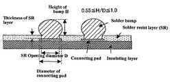
- a printed wiring board comprising a wiring substrate provided with at least one conductor circuit, a solder resist layer formed on the surface of the wiring substrate, covering the at least one conductor circuit, conductor pads formed on a part of the at least one conductor circuit exposed from respective openings provided in the solder resist layer for mounting electronic parts, and solder bumps formed on the respective conductor pads, wherein the conductor pads are arranged with a pitch of about 200 ⁇ m or less and the ratio (H/D) of a height H of the solder bump from the surface of the solder resist layer to an opening diameter D of the opening is about 0.55 to about 1.0.
- a printed wiring board comprising a wiring substrate provided with at least one conductor circuit, a solder resist layer formed on the surface of the wiring substrate, covering the at least one conductor circuit, conductor pads formed on a part of the at least one conductor circuit exposed from the respective openings provided in the solder resist for mounting electronic parts, solder bumps formed on the respective conductor pads, and an under fill material or resin 100 for sealing a gap or space defined between electronic parts mounted through the solder bumps and the solder resist layer, wherein the conductor pads are arranged with a pitch of about 200 ⁇ m or less and the ratio (H/D) of a height H of the solder bump from the surface of the solder resist layer to an opening diameter D of the opening is about 0.55 to about 1.0.
- the surface of the flattened solder resist layer can be further roughened, and it is desirable that surface roughness of the roughened surface (2nd uneven face) of the solder resist layer is smaller than the maximum surface roughness of the flattened surface and about 0.2 ⁇ m to about 0.5 ⁇ m at an arithmetic mean roughness (Ra).
- the conductor pad defined as a part of the conductor circuit exposed from the opening provided in the solder resist layer is formed in the form of a filled-via which is defined by a plated conductor completely filled within an opening provided in an interlaminar insulative resin layer positioned at the outermost layer, and an uneven amount of the filled-via surface exposed from the interlaminar insulative resin layer surface is about ⁇ 5 ⁇ m to about +5 ⁇ m in relation to the thickness of the conductor circuit formed on the interlaminar insulative resin layer.
- opening diameter (D) of the opening provided in the solder resist layer means a “diameter” of the opening when the opening side wall is not tapered, and means a diameter (of the opening upper part) of the opening exposed on the solder resist layer surface when the opening side wall is tapered.
- “maximum surface roughness” means, as schematically shown in FIG. 8 , in the electronic part mounting region, the maximum value in differences X 1 , X 2 , X 3 , X 4 , X 5 , . . . between the height of the solder resist layer on the conductor pad or the conductor circuit and that of the solder resist layer on an adjacent conductor pad non-forming portion or a conductor circuit non-forming portion.
- arithmetic mean roughness means arithmetic mean roughness (Ra) prescribed in JIS B0601, and the content of “arithmetic mean roughness” in JIS B0601 is incorporated herein by reference its entirety.
- FIG. 2 is a sectional view showing a state of mounting an IC chip on the printed wiring board shown in FIG. 1 and placing on a daughter board.
- FIGS. 3A to 3C are views explaining steps of forming solder bumps on the printed wiring board.
- FIGS. 4A to 4B are schematic views showing structure of an apparatus for mounting the solder balls on the wiring board.
- FIG. 5A is a schematic view explaining positioning of the printed wiring board
- FIG. 5B is a schematic view explaining supply of solder balls to mounting cylinders.
- FIG. 6A is a schematic view explaining assembly of solder balls by mounting cylinders
- FIG. 6B is a schematic view explaining assembly and guidance of solder balls by the mounting cylinders.
- FIG. 7A is a schematic view explaining dropping solder balls to connecting pads
- FIG. 7B is a schematic view explaining removal of solder balls by adsorbed-ball removing cylinder.
- FIG. 8 is a schematic view explaining maximum surface roughness of the solder resist layer surface.
- FIG. 9 is a schematic view explaining relation between bump height (H) and solder resist layer opening diameter (D) according to the present invention.
- FIGS. 10A to 10B are schematic views explaining unevenness of the filled-via surface as a connecting pad.
- FIGS. 11A to 11B are schematic views explaining connecting pad region.
- the printed wiring board As shown in FIG. 9 , at least one opening is provided in a solder resist layer (SR layer) formed on the outermost layer of a wiring board, a part of the conductor circuit exposed from the at least one opening is formed as connecting pads for mounting electronic parts, the connecting pads are arranged with a pitch of about 200 ⁇ m or less, and solder bumps are formed on the respective connecting pads, and a ratio (H/D) of a height H from the solder resist layer surface of the solder bump formed on the connecting pad to the opening diameter D is within a range of about 0.55 to about 1.0.
- SR layer solder resist layer
- a novel solder ball mounting method and a device thereof are used for manufacturing.
- the construction of one embodiment is explained by referring to FIG. 1 and FIG. 2 .
- FIG. 1 shows a sectional view of a printed wiring board 10
- FIG. 2 shows a state in which an IC chip 90 is mounted on the printed wiring board 10 and the printed wiring board 10 is mounted on a daughter board 94 .
- the printed wiring board 10 has a conductor circuit 34 formed on both surfaces of a core substrate 30 , and the respective conductor circuits are electrically connected through a plated through hole 36 .
- a conductor circuit 58 forming a conductor circuit layer through an interlaminar insulative resin layer 50 .
- the conductor circuit 58 is connected to the conductor circuit 34 through via hole 60 .
- a conductor circuit 158 is formed through an interlaminar insulative resin layer 150 .
- the conductor circuit 158 is connected to the conductor circuit 58 through a via hole 160 formed in an interlaminar insulative resin layer 150 .
- a solder resist layer 70 is formed by covering the conductor circuit 158 and the via hole 160 , and a connecting pad 75 is formed by forming a nickel plated layer 72 and a gold plated layer 74 on an opening 71 provided in the solder resist layer 71 .
- a solder bump 78 U On the connecting pad 75 of the top face is formed a solder bump 78 U and on the connecting pad 75 of the bottom face is formed a BGA (ball grid array) 78 D.
- the solder bump 78 U on the upper side of the printed wiring board 10 is connected to an electrode 92 of the IC chip 90 to form an IC mounted printed wiring board, and the IC mounted printed wiring board is connected to a land 96 of a daughter board 94 through the BGA 78 D.
- a height of the solder bump from the solder resist layer surface can be made comparatively large by making a ratio (H/D) of the height H of the solder bump to the opening diameter D of the opening about 0.55 or more, thereby easily deforming the solder bump in itself and enlarging volume (amount) of the solder.
- H/D ratio of the height H of the solder bump to the opening diameter D of the opening
- the solder fused between the adjacent solder bumps is hard to move by making a ratio (H/D) of the height H of the solder bump to the opening diameter D of the opening about 1.0 or less, thereby hardly moving the solder molten between adjacent solder bumps to control irregular solder bump height and to prevent short-circuit of adjacent solder bumps.
- connection reliability and insulation reliability are improved.
- the surface of the solder resist layer corresponding to at least electronic parts mounting region is flattened.
- the solder resist layer and the solder bump are different in thermal expansion coefficient, so that there are produced repeatedly contraction and expansion at the boundary vicinity between the solder bump and the solder resist layer.
- the volume of the solder resist layer in the bump vicinity is small to be easily broken. Therefore, by making flatness of the solder resist layer surface small to some extent, the volume of the solder resist layer where large stress is applied to is increased, bending portion where stress tends to concentrate is lessened, and heat cycle resistance can easily be improved.
- the flattened surface of the solder resist layer is desirably about 0.8 to about 3.0 ⁇ m in maximum surface roughness.
- the reason is that when the maximum surface roughness is within a range of about 0.8 to about 3.0 ⁇ m, crack is hardly generated in the solder resist in the vicinity of the conductor pad, and air (void) is hard to enter into the under fill resin 100 . As a result, insulation reliability and connection reliability are easily improved.
- Wettability of the under fill resin 100 is easily improved by applying the roughening treatment to the surface of the solder resist layer flattened to some extent, so that under fill resin 100 can be filled in a narrow gap portion in the boundary vicinity between the solder resist layer and the solder bump so as to improve connection reliability.
- the roughened surface of the solder resist layer is smaller than the maximum surface roughness of the flattened surface and about 0.2 to about 0.5 ⁇ m at an arithmetic mean roughness (Ra).
- the reason is that when the arithmetic mean roughness Ra is made within a range of about 0.2 to about 0.5 ⁇ m, adhesion to the under fill resin 100 can be increased, and flux residue and cleaning residue are hardly remained on the solder resist surface. As a result, insulation reliability and connection reliability are easily improved.
- thinning and low cost can be estimated without requiring any interposer.
- two connecting pads positioned at the center are formed in the form of a land right above the viahole 160
- two connecting pads adjacent thereto are formed in the form of pads adjacent to the land of the viahole 160
- further two connecting pads positioned at both ends are formed in the form of a pad consisting of a part of a wiring pattern of the conductor circuit 158 .
- connecting pads 75 formed on the lower surface of the substrate two connecting pads positioned at both ends are formed in the form of a land right above the viahole 160 , and four connecting pads positioned at the center are formed in the form of a pad adjacent to a land of the viahole 160 ,
- the viahole 160 as a connecting pad formed by the solder bump 78 U is preferably a filled-via, and the uneven amount of the filled-via surface exposed from the surface of the interlaminar insulative resin layer 150 is, as shown in FIGS. 10A to 10B , desirably within a range of about ⁇ 5 ⁇ m to about +5 ⁇ m in relation to the surface thickness of the conductor circuit 158 .
- the reason why the depressed or protruded amount of the filled-via surface is restricted to a mentioned above is due to the fact that when the depressed amount is about 5 ⁇ m ( ⁇ 5 ⁇ m) or less, the number of contact point defined by the solder ball and the connecting pad consisting of the filled-via is secured, and wettability in case of forming the solder bump is easily improved, and entanglement of voids within the bump and missing bump can be controlled, while when the protruded amount of the filled-via surface is about 5 ⁇ m (+5 ⁇ m) or less, the thickness of the conductor circuit 158 is controlled not to become large but easily adaptable for fine patterning.
- the “electronic parts mounting region” in the embodiment of the invention substantially corresponds to a region (hereinafter, simply called as “connecting pad region”) where conductor pads such as filled-via and the like for mounting electronic parts are provided.
- FIG. 11A shows a state of aligning all of the outermost peripheral connecting pads along each side of a rectangle among grid-like aligned connecting pads
- FIG. 11B shows a state of not aligning a part of the outermost peripheral connecting pads along each side of the rectangle, however, in either case, when the connecting pad region is made rectangle, a rectangle region determined to minimize an area of the region enclosing all connecting pads is called as “connecting pad region”.
- FIGS. 3A to 3C are views explaining the steps for forming the solder bumps on the printed wiring board 10 according to the present invention.
- a flux layer 80 is formed for covering conductor pads formed in the openings 71 provided in the solder resist layer 70 on the top face side of the printed wiring board, i.e. the connecting pads 75 by a printing method (see FIG. 3A ).
- solder balls 78 s for example, made by Hitachi Metals or Tamura
- solder ball loader described later on (see FIG. 3B ).
- solder ball is desirable to be about 40 ⁇ m or more and less than about 200 ⁇ m in diameter.
- each solder ball easily drops on the corresponding connecting pad because it is not too light in weight, and the solder balls are easily assembled in a cylinder member, thereby to control the presence of connecting pads with no solder balls mounted thereon.
- the solder ball having a diameter of less than or equal to about 80 ⁇ m is desirable.
- the pitch of the solder bumps corresponds to a pitch of the connecting pads, and when the pitch of the connecting pads is about 60 ⁇ m or more, manufacture of solder balls suitable for the pitch becomes possible. When the pitch of the connecting pads is about 200 ⁇ m or less, it becomes possible to obtain a printed wiring board adaptable for fine patterning or narrow pitching.
- FIG. 4A is an illustration showing the structure of the solder ball loader
- FIG. 4B is a view taken from an arrow B of the solder ball loader of FIG. 4A .
- the solder ball loader 20 comprises an XY ⁇ suction table 14 for positioning and holding the printed wiring board 10 , a shaft 12 for moving the XY ⁇ suction table 14 up and down, a ball aligning mask 16 with an opening corresponding to the connecting pad 75 of the printed wiring board, a mounting cylinder (cylinder member) 24 for guiding the solder balls moving on the ball aligning mask 16 , a suction box 26 for giving negative pressure to the mounting cylinder 24 , a solder ball removing cylinder 61 for recovering excessive solder balls, a suction box 66 for giving negative pressure to the solder ball removing cylinder 61 , an adsorbed ball removing and adsorbing device 68 for holding the collected solder balls, a mask clamp 44 for clamping the ball aligning mask 16 , an X-axis direction moving shaft 40 for sending the mounting cylinder 24 and the solder ball removing cylinder 61 to the X-axis direction, a moving shaft supporting guide 42 for supporting the X direction moving shaft 40 , an alignment
- a plurality of the mounting cylinders 24 and the solder ball removing cylinder 61 are arranged in the Y-axis direction by corresponding to size of the connecting pad regions. Further, the size may correspond to a plurality of the connecting pad areas.
- the Y-axis direction is expedient and may be aligned in the X-axis direction.
- the XY ⁇ suction table 14 functions as positioning, adsorption, maintenance and correction of the solder ball mounted printed wiring board 10 .
- the alignment camera 46 detects an alignment mark of the printed wiring board 10 on the XY ⁇ suction table 14 to regulate a position between the printed wiring board and the ball aligning mask 16 based on the detected position.
- the residue detecting sensor 18 detects the residue of the solder balls by an optical method.
- an alignment mark 34 M of the printed wiring board 10 is recognized by the alignment camera 46 , and the position of the printed wiring board 10 in relation to the ball aligning mask 16 is corrected by the suction table 14 . That is, openings 16 a of the ball aligning mask 16 are adjusted for corresponding to the connecting pads 75 of the printed wiring board 10 in position, respectively.
- the printed wiring board 10 for one is only shown, but actually, solder balls are mounted to a printed wiring board of worksheet size for constructing a plurality of wiring boards, and after forming solder bumps, the worksheet size board is cut into respective multilayer printed wiring boards
- solder balls 78 s are quantitatively supplied from a solder ball supplying device 22 to the side of the mounting cylinder 24 .
- solder ball use may be made of any commercial item (for example, made by Hitachi Metals) or, for example, solder balls may be manufactured according to the manufacturing device and method described in Japanese unexamined patent application No. 2001-226705.
- solder balls are placed on a metal plate (e.g. nickel plate of about 25 ⁇ m thick) having a square slit (opening) which length and breadth are smaller than a desired diameter of the solder ball by about 1 ⁇ m, and the solder balls are rolled thereon and dropped from the slit. Then, small balls having smaller diameters than the desired ones are removed. Thereafter, the solder balls remained on the metal plate are classified by a metal plate having a square slit which length and breadth are larger than the desired diameter of the solder ball by about 1 ⁇ m, and solder balls dropped from the slit are collected so as to obtain the solder balls each having a diameter substantially equal to the desired diameter.
- a metal plate e.g. nickel plate of about 25 ⁇ m thick
- solder balls are rolled thereon and dropped from the slit.
- small balls having smaller diameters than the desired ones are removed.
- solder balls remained on the metal plate are classified by a metal plate having a square slit
- the mounting cylinders 24 aligned along the Y axis of the printed wiring board 10 are sent to the horizontal direction along the X axis by means of the X axis moving shaft 40 .
- the solder balls 78 s assembled on the ball aligning mask 16 are moved with the movement of the mounting cylinder 24 , dropped to the corresponding connecting pads 75 of the printed wiring board 10 through the openings 16 a of the ball aligning mask 16 and loaded.
- the solder balls 78 s are successively aligned on the whole connecting pads on the side of the printed wiring board 10 .
- the excessive solder balls 78 s are guided to a place where no opening 16 a is provided on the ball aligning mask 16 , then adsorbed and removed by the solder ball removing cylinder 61 .
- the printed wiring board 10 is removed from the suction table 14 .
- the solder balls 78 s are assembled by positioning the mounting cylinder 24 on the upper part of the ball aligning mask 16 and adsorbing air from the suction portion 24 B on the top of the mounting cylinder 24 , the assembled solder balls 78 s are moved on the ball aligning mask 16 by moving the mounting cylinder 24 in the horizontal direction, and the solder balls 78 s can be dropped to the respective connecting pads 75 of the printed wiring board 10 through the respective openings 16 a of the ball aligning mask 16 .
- solder balls 78 s can certainly be mounted on the whole of the connecting pads 75 of the printed wiring board 10 . Further, since the solder balls 78 s can be moved with no contact, the solder balls can be mounted on the connecting pads 75 without injury, which is different from a printing method with the use of a conventional squeeze, and the solder bumps 78 U can be made having an equal height.
- the fine solder balls could certainly be placed on the connecting pads, even in the printed wiring board having such pitch alignment that the connecting pad pitch is about 60 to about 200 ⁇ m and the solder resist opening diameter is about 40 to about 150 ⁇ m, in the whole of bumps, stable bumps having substantially uniform heights ca be formed.
- solder balls are guided by suction force so as to prevent aggregation and adhesion of solder balls.
- works multilayer printed wiring board of work sheet size
- having various sizes can be used by adjusting number of the mounting cylinder 24 so as to be applied to many forms and small production.
- the mounting cylinders 24 are aligned in the Y-axis direction by corresponding to width of the work (printed wiring board of work sheet size), so that the solder balls can positively be mounted on the whole of connecting pads 75 of the printed wiring boards by simply sending a plurality of mounting cylinders 24 to the vertical direction (X-axis direction) in relation to the row direction.
- solder balls 78 s remained on the ball aligning mask 16 can be collected by the solder ball removing cylinder 61 , so that there are no problem such that excessive solder ball are remained to cause any trouble and the like.
- solder balls mounted on the connecting pads of the wiring substrate become solder bumps having predetermined height by means of a reflow treatment, IC chips are mounted on the substrate through such solder bumps, and the printed wiring board according to the present invention is manufactured.
- a double sided copper-clad laminate e.g. “MCL-E-67” made by Hitachi Chemical
- MCL-E-67 a double sided copper-clad laminate
- insulating layers and conductor circuit layers are alternately laminated by a known method (e.g. described in a book entitled “Build-up multilayer printed wiring board” (Kiyoshi Takagi) published by Nikkan Kogyo Shinbunsha on Jun.
- a group of connecting pads for mounting IC chips consisting a grid-like arrangement having thickness: 20 ⁇ m, diameter (conductor pad diameter): 150 ⁇ m, pitch: 200 ⁇ m, number: 50 ⁇ 40 (pieces) is formed within a connecting pad region of 150 mm 2 .
- a dimension of the region for forming these connecting pads was 150 mm 2 .
- Such connecting pad are formed by a method similar to that described in Japanese unexamined patent application No. 2000-357762.
- the disclosure of Japanese unexamined patent application No. 2000-357762 is incorporated herein by reference in its entirety.
- the pattern (opening diameter, pitch, arrangement, etc.) of a plated resist is changed.
- solder resist layer Formation of a solder resist layer is that screen printing is carried out under the following printing condition with the use of a commercial solder resist to form a solder resist layer having a thickness of about 15 to about 25 ⁇ m (on the connecting pad) for covering the connecting pad.
- solder resist layer having a thickness of 25 ⁇ m.
- a photo mask having a pattern (mask pattern) of openings of the solder resist thereon is exposed to ultraviolet ray of 100 to 1000 mJ under the state of adhering to the solder resist layer, and developed with a sodium carbonate solution (Na 2 CO 3 ) of 10 g/L, thereby forming the openings of about 120 ⁇ m in diameter on the corresponding connecting pads.
- a sodium carbonate solution Na 2 CO 3
- solder balls are placed on the suction table of a solder ball loader, alignment marks of the printed wiring board and the ball aligning mask are recognized by using a CCD camera, and alignment of the printed wiring board and the ball aligning mask is carried out.
- the ball aligning mask use is made of a metal mask made of Ni having openings of about 175 ⁇ m in diameter at the position corresponding to the connecting pads of the printed wiring board. Besides, it is possible to use ball aligning masks made of SUS and polyimide.
- an opening diameter formed in the ball aligning mask is preferably about 1.1 to about 1.5 times the ball diameter used, and a thickness of the ball aligning mask is preferably about 1 ⁇ 2 to about 3 ⁇ 4 of the diameter of the solder ball used.
- Sn/Pb is used for the solder ball
- Pb free solder consisting of at least one metal and Sn selected from the group of Ag, Co, In, Bi, Zn and the like.
- air is adsorbed from the top of the mounting cylinder, and the air speed in a gap between the mounting cylinder and the printed wiring board is regulated to about 5 to about 35 m/sec for assembling the solder balls within the mounting cylinder.
- the mounting cylinder is moved at about 10 to about 40 mm/sec to roll the solder balls, and the solder balls are dropped from the respective openings of the ball aligning mask and mounted on the corresponding connection pads.
- solder ball aligning mask and the printed wiring board are separately taken out of the solder ball loader, and finally, the printed wiring board is put in the reflow furnace set at 230° C. to form a solder bump.
- a height of the solder bump protruded from the solder resist surface is measured by a laser microscope (“VX-8500” made by KEYENCE or “WYKO NT-2000” made by Veeco).
- measurement points are four corners and a center of a rectangle, i.e. four solder bumps located at the four corners of a rectangle defined by the connecting pad group and a solder bump substantially positioned at the center of the rectangle are measured, that is to say, five solder bumps in total are measured at this time.
- the minimum value of the solder bump height is 66 ⁇ m and the maximum value thereof is 70 ⁇ m.
- an IC chip is mounted through the solder bumps, and the IC chip mounted printed wiring board is manufactured by filling a commercial under fill resin 100 between the IC chip and the solder resist.
- the mask pattern of a photo mask in case of forming a solder resist opening is changed to change the solder resist opening diameter to 90 ⁇ m
- the printing condition (mesh of screen and printing speed) of the solder resist is regulated
- film thickness of the solder resist is made 10 ⁇ m
- the solder ball having a diameter of 90 ⁇ m is mounted with the use of the ball aligning mask having an opening diameter of 110 ⁇ m
- a printed wiring board is manufactured in the same manner as in Example 1.
- the minimum value of the solder bump height becomes 46 ⁇ m and the maximum value thereof becomes 49 ⁇ m.
- the mask pattern of the photo mask in case of forming a solder resist opening is changed to change the solder resist opening diameter to 60 ⁇ m
- the printing condition (mesh of screen and printing speed) of the solder resist is regulated
- film thickness of the solder resist is made 10 ⁇ m
- the solder ball having a diameter of 50 ⁇ m is mounted with the use of the ball aligning mask having an opening diameter of 60 ⁇ m
- a printed wiring board is manufactured in the same manner as in Example 1.
- the minimum value of the solder bump height becomes 31 ⁇ m and the maximum value thereof becomes 34 ⁇ m.
- solder ball having a diameter of 160 ⁇ m is mounted with the use of the ball aligning mask having an opening diameter of 190 ⁇ m
- a printed wiring board is manufactured in the same manner as in Example 1.
- the minimum value of the solder bump height becomes 84 ⁇ m and the maximum value thereof becomes 87 ⁇ m.
- solder ball having a diameter of 215 ⁇ m is mounted with the use of the ball aligning mask having an opening diameter of 260 ⁇ m, a printed wiring board is manufactured in the same manner as in Example 2.
- the minimum value of the solder bump height becomes 100 ⁇ m and the maximum value thereof becomes 180 ⁇ m.
- solder ball having a diameter of 170 ⁇ m is mounted with the use of the ball aligning mask having an opening diameter of 200 ⁇ m, a printed wiring board is manufactured in the same manner as in Example 8. As a result, the minimum value of the solder bump height becomes 75 ⁇ m and the maximum value thereof becomes 160 ⁇ m.
- solder ball having a diameter of 120 ⁇ m is mounted with the use of the ball aligning mask having an opening diameter of 150 ⁇ m, a printed wiring board is manufactured in the same manner as in Example 12. As a result, the minimum value of the solder bump height becomes 75 ⁇ m and the maximum value thereof becomes 90 ⁇ m.
- Examples 37 to 45 printed wiring boards made by applying the following flattening treatment to the solder resist layer surface are manufactured, and these are denoted as Examples 37 to 45.
- a connecting pad region for mounting IC chip (region area: 1200 mm 2 , connecting pad number: 30000) is measured by means of a surface roughness measuring instrument (e.g. “SURFCOM 480A” made by Tokyo Seimitsu or “WYKO N-2500” by Veeco) to examine uneven amount (see FIG. 8 ) due to the presence or absence of conductor pads. As a result, the uneven amount of the solder resist layer surface becomes 7.2 to 9.8 ⁇ m.
- a surface roughness measuring instrument e.g. “SURFCOM 480A” made by Tokyo Seimitsu or “WYKO N-2500” by Veeco
- PET polyethylene terephthalate
- maximum uneven amount and “minimum uneven amount” mentioned herein mean, as shown in FIG. 8 , maximum value and minimum value of differences X 1 , X 2 , X 3 , X 4 , X 5 . . . between height of the solder resist layer on the conductor pad or conductor circuit and that of the solder resist layer of adjacent conductor pad non-forming part or conductor circuit non-forming part in the electronic part mounting region.
- An uneven amount of the surface before flattening the solder resist layer obtained in this example is comparatively large such as about 6.6 to 10.2 ⁇ m, but the amount of the flattened surface is small such as about 0.7 to 3.0 ⁇ m.
- An uneven amount of the surface before flattening the solder resist layer obtained in this example is comparatively large such as about 8.4 to 9.3 ⁇ m, but that of the flattened surface is small such as about 0.8 to 3.1 ⁇ m.
- An uneven amount of the surface before flattening the solder resist layer obtained in this example is large such as about 8.2 to 9.6 ⁇ m, but that of the flattened surface is small such as about 0.7 to 3.2 ⁇ m.
- An uneven amount of the surface before flattening the solder resist layer obtained in this example is comparatively large such as about 9.9 to 10.2 ⁇ m, but that of the flattened surface is small such as about 0.8 to 3.3 ⁇ m.
- An uneven amount of the surface before flattening the solder resist layer obtained in this example is comparatively large such as about 8.3 to 10.3 ⁇ m, but that of the flattened surface is small such as about 0.7 to 3.0 ⁇ m.
- An uneven amount of the surface before flattening the solder resist layer obtained in this example is comparatively large such as about 9.1 to 9.8 ⁇ m. but that of the flattened surface is small such as about 0.5 to 3.1 ⁇ m.
- An uneven amount of the surface before flattening the solder resist layer obtained in this example is comparatively large such as about 8.1 to 10.2 ⁇ m, but that of the flattened surface is small such as about 0.8 to 3.0 ⁇ m.
- An uneven amount of the surface before flattening the solder resist layer obtained in this example is comparatively large such as about 9.6 to 10.3 ⁇ m, but that of the flattened surface is small such as about 0.7 to 3.0 ⁇ m.
- surface roughness of the solder resist surface is randomly measured at 10 spots by surface roughness measuring instrument (for example, “SURFCOM 480A” made by Tokyo Seimitsu or “WYKO N-2500” made by Veeco).
- surface roughness measuring instrument for example, “SURFCOM 480A” made by Tokyo Seimitsu or “WYKO N-2500” made by Veeco.
- surface roughness (Ra) mentioned here means “arithmetic mean roughness (Ra)” prescribed by JIS B0601, but Ra within a range of the above measuring result is mentioned that the smallest Ra is Ra(min) and the largest one is Ra(max) in measured 10 spots.
- surface roughness is measured at random 10 spots in the solder resist layer surface corresponding to the conductor circuit (pad) forming region and the solder resist layer surface corresponding to the conductor circuit non-forming region, but not measured in the boundary vicinity of the conductor circuit forming region and the conductor circuit non-forming region.
- Example 39 Except that roughening treatment is further applied to the solder resist layer surface with the following condition after flattening treatment, a printed wiring board is manufactured in the same manner as in Example 39.
- Example 40 Except that roughening treatment is further applied to the solder resist layer surface with the following condition after flattening treatment, a printed wiring board is manufactured in the same manner as in Example 40.
- Example 44 Except that roughening treatment is further applied to the solder resist layer surface with the following condition after flattening treatment, a printed wiring board is manufactured in the same manner as in Example 44.
- Example 45 Except that roughening treatment is further applied to the solder resist layer surface with the following condition after flattening treatment, a printed wiring board is manufactured in the same manner as in Example 45.
- connection reliability is improved.
- unevenness of the solder resist layer surface due to the presence or absence of the connecting pad positioned beneath the solder resist is flattened, and when roughness of the flattened surface is about 0.8 to about 3 ⁇ m of maximum surface roughness (uneven amount), connection reliability is improved.
- connection reliability is further improved. It is assumed that adhesion between the under fill resin 100 and the solder resist layer surface is easily improved, or flux and flux cleaning solvent are hard to remain within a recess of the surface.
- the printed wiring boards manufactured according to Examples 1 to 54 and Comparative Examples 1 to 24 are left in atmosphere of temperature: 85° C. and humidity: 85% by applying voltage of 3.3V between adjacent and not shorted solder bumps for 50 hours. Thereafter, insulation resistance between the voltage-applied solder bumps is measured.
- insulation performance is “good (O)” and when insulation resistance is less than 10 7 ⁇ , insulation performance is “no good (x)” for evaluation.
- voids within solder bumps are observed by using an X-ray television system (“SMX-100” made by Shimazu Corporation) and number of voids is measured. 100 solder bumps are randomly selected, but no void is observed.
- SMX-100 X-ray television system
- an IC mounted printed wiring board is manufactured in the same manner as in Examples 1 to 54, each of these examples is conducted to heat cycle test, HAST test and observation of voids in solder bump in the same manner as in Examples 1 to 54, and the same results as Examples 1 to 54 can be obtained.
Landscapes
- Engineering & Computer Science (AREA)
- Microelectronics & Electronic Packaging (AREA)
- Computer Hardware Design (AREA)
- Power Engineering (AREA)
- Physics & Mathematics (AREA)
- Condensed Matter Physics & Semiconductors (AREA)
- General Physics & Mathematics (AREA)
- Manufacturing & Machinery (AREA)
- Ceramic Engineering (AREA)
- Electric Connection Of Electric Components To Printed Circuits (AREA)
Priority Applications (2)
| Application Number | Priority Date | Filing Date | Title |
|---|---|---|---|
| US12/713,274 US8003897B2 (en) | 2005-06-30 | 2010-02-26 | Printed wiring board |
| US12/952,537 US8832935B2 (en) | 2005-06-30 | 2010-11-23 | Method of manufacturing a printed wiring board |
Applications Claiming Priority (2)
| Application Number | Priority Date | Filing Date | Title |
|---|---|---|---|
| JP2005192862 | 2005-06-30 | ||
| JP2005-192862 | 2005-06-30 |
Related Child Applications (1)
| Application Number | Title | Priority Date | Filing Date |
|---|---|---|---|
| US12/713,274 Continuation US8003897B2 (en) | 2005-06-30 | 2010-02-26 | Printed wiring board |
Publications (2)
| Publication Number | Publication Date |
|---|---|
| US20070096327A1 US20070096327A1 (en) | 2007-05-03 |
| US7714233B2 true US7714233B2 (en) | 2010-05-11 |
Family
ID=37604518
Family Applications (3)
| Application Number | Title | Priority Date | Filing Date |
|---|---|---|---|
| US11/476,557 Active US7714233B2 (en) | 2005-06-30 | 2006-06-29 | Printed wiring board |
| US12/713,274 Active US8003897B2 (en) | 2005-06-30 | 2010-02-26 | Printed wiring board |
| US12/952,537 Active 2029-02-20 US8832935B2 (en) | 2005-06-30 | 2010-11-23 | Method of manufacturing a printed wiring board |
Family Applications After (2)
| Application Number | Title | Priority Date | Filing Date |
|---|---|---|---|
| US12/713,274 Active US8003897B2 (en) | 2005-06-30 | 2010-02-26 | Printed wiring board |
| US12/952,537 Active 2029-02-20 US8832935B2 (en) | 2005-06-30 | 2010-11-23 | Method of manufacturing a printed wiring board |
Country Status (7)
| Country | Link |
|---|---|
| US (3) | US7714233B2 (zh) |
| EP (1) | EP1887845A4 (zh) |
| JP (1) | JP5021472B2 (zh) |
| KR (1) | KR100905686B1 (zh) |
| CN (2) | CN101171894B (zh) |
| TW (1) | TW200738090A (zh) |
| WO (1) | WO2007004657A1 (zh) |
Cited By (10)
| Publication number | Priority date | Publication date | Assignee | Title |
|---|---|---|---|---|
| US20080298038A1 (en) * | 2007-05-30 | 2008-12-04 | Shinko Electric Industries Co., Ltd. | Wiring board and its fabricating method |
| US20100155129A1 (en) * | 2005-06-30 | 2010-06-24 | Ibiden Co., Ltd. | Printed wiring board |
| US20110101491A1 (en) * | 2007-09-25 | 2011-05-05 | Oswald Skeete | Integrated circuit packages including high density bump-less build up layers and a lesser density core or coreless substrate |
| US20110195223A1 (en) * | 2010-02-11 | 2011-08-11 | Qualcomm Incorporated | Asymmetric Front/Back Solder Mask |
| US8624132B2 (en) | 2005-06-30 | 2014-01-07 | Ibiden Co., Ltd. | Printed wiring board |
| US9480170B2 (en) | 2006-01-27 | 2016-10-25 | Ibiden Co., Ltd. | Printed wiring board and a method of manufacturing a printed wiring board |
| US20170186722A1 (en) * | 2015-12-24 | 2017-06-29 | Intel Corporation | Systems and processes for measuring thickness values of semiconductor substrates |
| US9891523B2 (en) | 2014-06-30 | 2018-02-13 | Taiyo Ink Mfg. Co., Ltd. | Photosensitive dry film and process for producing printed wiring board using the same |
| US10257942B1 (en) * | 2009-08-06 | 2019-04-09 | Amkor Technology, Inc. | Stackable variable height via package and method |
| US10388309B2 (en) | 2017-05-17 | 2019-08-20 | Nhk Spring Co., Ltd. | Circuit member of disk drive suspension having a metal base and a side pad portion electrically insulated from the metal base |
Families Citing this family (38)
| Publication number | Priority date | Publication date | Assignee | Title |
|---|---|---|---|---|
| CN101826496B (zh) * | 2005-05-23 | 2015-03-18 | 揖斐电株式会社 | 印刷线路板及其制造方法 |
| TW200746964A (en) * | 2006-01-27 | 2007-12-16 | Ibiden Co Ltd | Method of manufacturing printed wiring board |
| US7969005B2 (en) * | 2007-04-27 | 2011-06-28 | Sanyo Electric Co., Ltd. | Packaging board, rewiring, roughened conductor for semiconductor module of a portable device, and manufacturing method therefor |
| US7982137B2 (en) * | 2007-06-27 | 2011-07-19 | Hamilton Sundstrand Corporation | Circuit board with an attached die and intermediate interposer |
| TWI463582B (zh) * | 2007-09-25 | 2014-12-01 | Ngk Spark Plug Co | 具有焊接凸塊之配線基板的製造方法 |
| KR101551898B1 (ko) * | 2007-10-05 | 2015-09-09 | 신꼬오덴기 고교 가부시키가이샤 | 배선 기판, 반도체 장치 및 이들의 제조 방법 |
| KR100965341B1 (ko) * | 2007-12-20 | 2010-06-22 | 삼성전기주식회사 | 인쇄회로기판의 제조방법 |
| KR100992181B1 (ko) | 2007-12-26 | 2010-11-04 | 삼성전기주식회사 | 패키지용 기판 및 그 제조방법 |
| US7759137B2 (en) * | 2008-03-25 | 2010-07-20 | Stats Chippac, Ltd. | Flip chip interconnection structure with bump on partial pad and method thereof |
| US9345148B2 (en) | 2008-03-25 | 2016-05-17 | Stats Chippac, Ltd. | Semiconductor device and method of forming flipchip interconnection structure with bump on partial pad |
| TWI363585B (en) * | 2008-04-02 | 2012-05-01 | Advanced Semiconductor Eng | Method for manufacturing a substrate having embedded component therein |
| EP2157841A4 (en) | 2008-05-30 | 2011-11-02 | Ibiden Co Ltd | MOUNTING DEVICE FOR A SOLDERING BALL |
| JP5290215B2 (ja) * | 2010-02-15 | 2013-09-18 | ルネサスエレクトロニクス株式会社 | 半導体装置、半導体パッケージ、インタポーザ、及びインタポーザの製造方法 |
| JP5623308B2 (ja) * | 2010-02-26 | 2014-11-12 | 日本特殊陶業株式会社 | 多層配線基板及びその製造方法 |
| US20120160542A1 (en) * | 2010-12-22 | 2012-06-28 | Oluwafemi Olufemi B | Crosstalk reduction on microstrip routing |
| JP2012169591A (ja) | 2011-01-24 | 2012-09-06 | Ngk Spark Plug Co Ltd | 多層配線基板 |
| US8643154B2 (en) | 2011-01-31 | 2014-02-04 | Ibiden Co., Ltd. | Semiconductor mounting device having multiple substrates connected via bumps |
| US8692129B2 (en) * | 2011-03-31 | 2014-04-08 | Ibiden Co., Ltd. | Package-substrate-mounting printed wiring board and method for manufacturing the same |
| KR101936451B1 (ko) * | 2011-05-09 | 2019-01-08 | 엔테그리스, 아이엔씨. | 미세다공성 막 층들 및 나노섬유 층을 포함하는 다공성 복합막 |
| US8653658B2 (en) | 2011-11-30 | 2014-02-18 | Taiwan Semiconductor Manufacturing Company, Ltd. | Planarized bumps for underfill control |
| CN102543930A (zh) * | 2012-02-03 | 2012-07-04 | 昆山美微电子科技有限公司 | 电铸晶圆凸块 |
| JP5502139B2 (ja) * | 2012-05-16 | 2014-05-28 | 日本特殊陶業株式会社 | 配線基板 |
| US8970035B2 (en) | 2012-08-31 | 2015-03-03 | Taiwan Semiconductor Manufacturing Company, Ltd. | Bump structures for semiconductor package |
| US9673131B2 (en) | 2013-04-09 | 2017-06-06 | Intel Corporation | Integrated circuit package assemblies including a glass solder mask layer |
| KR101734425B1 (ko) * | 2013-09-24 | 2017-05-11 | 주식회사 엘지화학 | 드라이 필름 솔더 레지스트의 제조 방법과, 이에 사용되는 필름 적층체 |
| JP6320066B2 (ja) * | 2014-02-13 | 2018-05-09 | イビデン株式会社 | ボール搭載用マスクおよびボール搭載装置 |
| JP2016012002A (ja) * | 2014-06-27 | 2016-01-21 | 日立化成株式会社 | 感光性樹脂組成物の硬化物、それに用いる感光性樹脂組成物及び半導体装置搭載用基板の製造方法、半導体装置の製造方法 |
| JP6329027B2 (ja) * | 2014-08-04 | 2018-05-23 | ミネベアミツミ株式会社 | フレキシブルプリント基板 |
| CN104185360B (zh) * | 2014-08-18 | 2017-05-24 | 深圳市华星光电技术有限公司 | 一种印刷电路板及其设计方法 |
| JP2016076533A (ja) * | 2014-10-03 | 2016-05-12 | イビデン株式会社 | バンプ付きプリント配線板およびその製造方法 |
| JP6230520B2 (ja) * | 2014-10-29 | 2017-11-15 | キヤノン株式会社 | プリント回路板及び電子機器 |
| JP6175205B1 (ja) * | 2017-02-01 | 2017-08-02 | 太陽インキ製造株式会社 | 感光性フィルム、感光性フィルム積層体およびそれらを用いて形成された硬化物 |
| JP6199524B1 (ja) * | 2017-07-03 | 2017-09-20 | 太陽インキ製造株式会社 | 感光性フィルム、感光性フィルム積層体およびそれらを用いて形成された硬化物 |
| JP6199525B1 (ja) * | 2017-07-03 | 2017-09-20 | 太陽インキ製造株式会社 | 感光性フィルム、感光性フィルム積層体およびそれらを用いて形成された硬化物 |
| JP2019140174A (ja) * | 2018-02-07 | 2019-08-22 | イビデン株式会社 | プリント配線板およびプリント配線板の製造方法 |
| CN109688720B (zh) * | 2018-12-30 | 2020-09-01 | 北京康普锡威科技有限公司 | 预制焊料的pcb板的制备方法及pcb板 |
| CN116801482B (zh) * | 2022-03-18 | 2024-05-10 | 华为技术有限公司 | 电路板组件及其加工方法、电子设备 |
| CN114585175B (zh) * | 2022-04-29 | 2022-07-15 | 广东科翔电子科技股份有限公司 | 一种Mini-LED焊盘加高方法 |
Citations (20)
| Publication number | Priority date | Publication date | Assignee | Title |
|---|---|---|---|---|
| JPS59996A (ja) | 1982-06-25 | 1984-01-06 | 株式会社日立製作所 | 基板の接続構造 |
| JPH05121411A (ja) | 1991-10-25 | 1993-05-18 | Rohm Co Ltd | 電子部品における接続用バンプの形成方法 |
| US5329423A (en) | 1993-04-13 | 1994-07-12 | Scholz Kenneth D | Compressive bump-and-socket interconnection scheme for integrated circuits |
| JPH1140908A (ja) | 1997-07-22 | 1999-02-12 | Ibiden Co Ltd | プリント配線板 |
| US6046910A (en) * | 1998-03-18 | 2000-04-04 | Motorola, Inc. | Microelectronic assembly having slidable contacts and method for manufacturing the assembly |
| US6256207B1 (en) * | 1998-07-06 | 2001-07-03 | Shinko Electric Industries Co., Ltd. | Chip-sized semiconductor device and process for making same |
| JP2002208778A (ja) | 2001-01-10 | 2002-07-26 | Ibiden Co Ltd | 多層プリント配線板 |
| JP2002217531A (ja) | 2001-01-12 | 2002-08-02 | Ibiden Co Ltd | 多層プリント配線板の製造方法 |
| US6443351B1 (en) * | 2000-05-15 | 2002-09-03 | Siliconware Precision Industries Co., Ltd. | Method of achieving solder ball coplanarity on ball grid array integrated circuit package |
| US20030214795A1 (en) | 2002-05-17 | 2003-11-20 | Fujitsu Limited | Electronic component with bump electrodes, and manufacturing method thereof |
| US6719185B2 (en) * | 2001-06-27 | 2004-04-13 | Ngk Spark Plug Co., Ltd. | Substrate with top-flattened solder bumps and method for manufacturing the same |
| US6753480B2 (en) | 2001-10-12 | 2004-06-22 | Ultratera Corporation | Printed circuit board having permanent solder mask |
| JP2004179578A (ja) | 2002-11-29 | 2004-06-24 | Ngk Spark Plug Co Ltd | 配線基板及びその製造方法 |
| JP2004207370A (ja) | 2002-12-24 | 2004-07-22 | Cmk Corp | プリント配線板の製造方法 |
| US20040209451A1 (en) | 2003-04-15 | 2004-10-21 | Harima Chemicals, Inc. | Solder deposition method and solder bump forming method |
| US6809268B2 (en) * | 2000-07-31 | 2004-10-26 | Ngk Spark Plug Co., Ltd. | Printed wiring substrate and method for fabricating the same |
| US7087991B2 (en) * | 2002-01-16 | 2006-08-08 | Via Technologies, Inc. | Integrated circuit package and method of manufacture |
| US20060244142A1 (en) * | 2005-04-27 | 2006-11-02 | Bernd Waidhas | Electronic component and electronic configuration |
| US20070086147A1 (en) | 2005-06-30 | 2007-04-19 | Ibiden Co., Ltd. | Printed wiring board |
| US7279771B2 (en) | 2004-03-31 | 2007-10-09 | Shinko Electric Industries Co., Ltd. | Wiring board mounting a capacitor |
Family Cites Families (26)
| Publication number | Priority date | Publication date | Assignee | Title |
|---|---|---|---|---|
| US5118027A (en) * | 1991-04-24 | 1992-06-02 | International Business Machines Corporation | Method of aligning and mounting solder balls to a substrate |
| JPH1174403A (ja) * | 1997-08-28 | 1999-03-16 | Mitsubishi Electric Corp | 半導体装置 |
| WO2000010369A1 (fr) * | 1998-08-10 | 2000-02-24 | Fujitsu Limited | Realisation de bossages de soudure, methode de montage d'un dispositif electronique et structure de montage pour ce dispositif |
| JP3213292B2 (ja) * | 1999-07-12 | 2001-10-02 | ソニーケミカル株式会社 | 多層基板、及びモジュール |
| US6563210B2 (en) * | 2000-12-19 | 2003-05-13 | Intel Corporation | Parallel plane substrate |
| TWI293315B (en) * | 2000-12-26 | 2008-02-11 | Ngk Spark Plug Co | Wiring substrate |
| JP2002290030A (ja) * | 2001-03-23 | 2002-10-04 | Ngk Spark Plug Co Ltd | 配線基板 |
| DE10138042A1 (de) | 2001-08-08 | 2002-11-21 | Infineon Technologies Ag | Elektronisches Bauteil und Verfahren zu seiner Herstellung |
| JP3910387B2 (ja) * | 2001-08-24 | 2007-04-25 | 新光電気工業株式会社 | 半導体パッケージ及びその製造方法並びに半導体装置 |
| JP2003218272A (ja) * | 2002-01-25 | 2003-07-31 | Sony Corp | 高周波モジュール及びその製造方法 |
| JP4209178B2 (ja) * | 2002-11-26 | 2009-01-14 | 新光電気工業株式会社 | 電子部品実装構造及びその製造方法 |
| JP4006699B2 (ja) * | 2003-04-22 | 2007-11-14 | 日立金属株式会社 | 微小ボール搭載用マスクおよび微小ボールの搭載方法 |
| WO2004103039A1 (ja) * | 2003-05-19 | 2004-11-25 | Dai Nippon Printing Co., Ltd. | 両面配線基板および両面配線基板の製造方法並びに多層配線基板 |
| KR100520961B1 (ko) * | 2003-05-30 | 2005-10-17 | 엘지전자 주식회사 | 인쇄회로기판의 제조방법 |
| TWI222687B (en) * | 2003-08-14 | 2004-10-21 | Advanced Semiconductor Eng | Semiconductor chip with bumps and method for manufacturing the same |
| TWI335195B (en) * | 2003-12-16 | 2010-12-21 | Ngk Spark Plug Co | Multilayer wiring board |
| JP4860113B2 (ja) * | 2003-12-26 | 2012-01-25 | ルネサスエレクトロニクス株式会社 | 半導体集積回路装置の製造方法 |
| TWI240389B (en) | 2004-05-06 | 2005-09-21 | Advanced Semiconductor Eng | High-density layout substrate for flip-chip package |
| CN100367491C (zh) * | 2004-05-28 | 2008-02-06 | 日本特殊陶业株式会社 | 中间基板 |
| US7626829B2 (en) * | 2004-10-27 | 2009-12-01 | Ibiden Co., Ltd. | Multilayer printed wiring board and manufacturing method of the multilayer printed wiring board |
| JP2006216713A (ja) * | 2005-02-02 | 2006-08-17 | Ibiden Co Ltd | 多層プリント配線板 |
| TWI414218B (zh) * | 2005-02-09 | 2013-11-01 | Ngk Spark Plug Co | 配線基板及配線基板內建用之電容器 |
| CN101826496B (zh) | 2005-05-23 | 2015-03-18 | 揖斐电株式会社 | 印刷线路板及其制造方法 |
| CN101171894B (zh) * | 2005-06-30 | 2010-05-19 | 揖斐电株式会社 | 印刷线路板 |
| JP4838068B2 (ja) * | 2005-09-01 | 2011-12-14 | 日本特殊陶業株式会社 | 配線基板 |
| CN101283631B (zh) * | 2005-12-20 | 2010-06-09 | 揖斐电株式会社 | 印刷线路板的制造方法 |
-
2006
- 2006-06-28 CN CN2006800148623A patent/CN101171894B/zh active Active
- 2006-06-28 CN CN201010138568A patent/CN101868120A/zh active Pending
- 2006-06-28 JP JP2007524083A patent/JP5021472B2/ja active Active
- 2006-06-28 WO PCT/JP2006/313342 patent/WO2007004657A1/ja active Application Filing
- 2006-06-28 EP EP06780769A patent/EP1887845A4/en not_active Withdrawn
- 2006-06-29 US US11/476,557 patent/US7714233B2/en active Active
- 2006-06-30 TW TW095123798A patent/TW200738090A/zh unknown
-
2007
- 2007-10-31 KR KR1020077025324A patent/KR100905686B1/ko active IP Right Grant
-
2010
- 2010-02-26 US US12/713,274 patent/US8003897B2/en active Active
- 2010-11-23 US US12/952,537 patent/US8832935B2/en active Active
Patent Citations (24)
| Publication number | Priority date | Publication date | Assignee | Title |
|---|---|---|---|---|
| JPS59996A (ja) | 1982-06-25 | 1984-01-06 | 株式会社日立製作所 | 基板の接続構造 |
| JPH05121411A (ja) | 1991-10-25 | 1993-05-18 | Rohm Co Ltd | 電子部品における接続用バンプの形成方法 |
| US5329423A (en) | 1993-04-13 | 1994-07-12 | Scholz Kenneth D | Compressive bump-and-socket interconnection scheme for integrated circuits |
| JPH1140908A (ja) | 1997-07-22 | 1999-02-12 | Ibiden Co Ltd | プリント配線板 |
| US6046910A (en) * | 1998-03-18 | 2000-04-04 | Motorola, Inc. | Microelectronic assembly having slidable contacts and method for manufacturing the assembly |
| US6256207B1 (en) * | 1998-07-06 | 2001-07-03 | Shinko Electric Industries Co., Ltd. | Chip-sized semiconductor device and process for making same |
| US6443351B1 (en) * | 2000-05-15 | 2002-09-03 | Siliconware Precision Industries Co., Ltd. | Method of achieving solder ball coplanarity on ball grid array integrated circuit package |
| US6809268B2 (en) * | 2000-07-31 | 2004-10-26 | Ngk Spark Plug Co., Ltd. | Printed wiring substrate and method for fabricating the same |
| JP2002208778A (ja) | 2001-01-10 | 2002-07-26 | Ibiden Co Ltd | 多層プリント配線板 |
| JP2002217531A (ja) | 2001-01-12 | 2002-08-02 | Ibiden Co Ltd | 多層プリント配線板の製造方法 |
| US6719185B2 (en) * | 2001-06-27 | 2004-04-13 | Ngk Spark Plug Co., Ltd. | Substrate with top-flattened solder bumps and method for manufacturing the same |
| US6753480B2 (en) | 2001-10-12 | 2004-06-22 | Ultratera Corporation | Printed circuit board having permanent solder mask |
| US6933448B2 (en) * | 2001-10-12 | 2005-08-23 | S & S Technology Corporation | Printed circuit board having permanent solder mask |
| US7087991B2 (en) * | 2002-01-16 | 2006-08-08 | Via Technologies, Inc. | Integrated circuit package and method of manufacture |
| US20030214795A1 (en) | 2002-05-17 | 2003-11-20 | Fujitsu Limited | Electronic component with bump electrodes, and manufacturing method thereof |
| US7189927B2 (en) * | 2002-05-17 | 2007-03-13 | Fujitsu Limited | Electronic component with bump electrodes, and manufacturing method thereof |
| JP2004179578A (ja) | 2002-11-29 | 2004-06-24 | Ngk Spark Plug Co Ltd | 配線基板及びその製造方法 |
| JP2004207370A (ja) | 2002-12-24 | 2004-07-22 | Cmk Corp | プリント配線板の製造方法 |
| US20040209451A1 (en) | 2003-04-15 | 2004-10-21 | Harima Chemicals, Inc. | Solder deposition method and solder bump forming method |
| JP2004319676A (ja) | 2003-04-15 | 2004-11-11 | Harima Chem Inc | はんだ析出方法およびはんだバンプ形成方法 |
| US7452797B2 (en) | 2003-04-15 | 2008-11-18 | Harima Chemicals, Inc. | Solder deposition method and solder bump forming method |
| US7279771B2 (en) | 2004-03-31 | 2007-10-09 | Shinko Electric Industries Co., Ltd. | Wiring board mounting a capacitor |
| US20060244142A1 (en) * | 2005-04-27 | 2006-11-02 | Bernd Waidhas | Electronic component and electronic configuration |
| US20070086147A1 (en) | 2005-06-30 | 2007-04-19 | Ibiden Co., Ltd. | Printed wiring board |
Cited By (15)
| Publication number | Priority date | Publication date | Assignee | Title |
|---|---|---|---|---|
| US20100155129A1 (en) * | 2005-06-30 | 2010-06-24 | Ibiden Co., Ltd. | Printed wiring board |
| US8003897B2 (en) * | 2005-06-30 | 2011-08-23 | Ibiden Co., Ltd. | Printed wiring board |
| US8624132B2 (en) | 2005-06-30 | 2014-01-07 | Ibiden Co., Ltd. | Printed wiring board |
| US9480170B2 (en) | 2006-01-27 | 2016-10-25 | Ibiden Co., Ltd. | Printed wiring board and a method of manufacturing a printed wiring board |
| US20080298038A1 (en) * | 2007-05-30 | 2008-12-04 | Shinko Electric Industries Co., Ltd. | Wiring board and its fabricating method |
| US8357860B2 (en) * | 2007-05-30 | 2013-01-22 | Shinko Electric Industries Co., Ltd. | Wiring board having a connecting pad area which is smaller than a surface plating layer area |
| US9258899B2 (en) | 2007-05-30 | 2016-02-09 | Shinko Electric Industries Co., Ltd. | Method of fabricating a wiring board |
| US9941245B2 (en) * | 2007-09-25 | 2018-04-10 | Intel Corporation | Integrated circuit packages including high density bump-less build up layers and a lesser density core or coreless substrate |
| US20110101491A1 (en) * | 2007-09-25 | 2011-05-05 | Oswald Skeete | Integrated circuit packages including high density bump-less build up layers and a lesser density core or coreless substrate |
| US10257942B1 (en) * | 2009-08-06 | 2019-04-09 | Amkor Technology, Inc. | Stackable variable height via package and method |
| US20110195223A1 (en) * | 2010-02-11 | 2011-08-11 | Qualcomm Incorporated | Asymmetric Front/Back Solder Mask |
| US9891523B2 (en) | 2014-06-30 | 2018-02-13 | Taiyo Ink Mfg. Co., Ltd. | Photosensitive dry film and process for producing printed wiring board using the same |
| US20170186722A1 (en) * | 2015-12-24 | 2017-06-29 | Intel Corporation | Systems and processes for measuring thickness values of semiconductor substrates |
| US10269758B2 (en) * | 2015-12-24 | 2019-04-23 | Intel Corporation | Systems and processes for measuring thickness values of semiconductor substrates |
| US10388309B2 (en) | 2017-05-17 | 2019-08-20 | Nhk Spring Co., Ltd. | Circuit member of disk drive suspension having a metal base and a side pad portion electrically insulated from the metal base |
Also Published As
| Publication number | Publication date |
|---|---|
| CN101868120A (zh) | 2010-10-20 |
| US20100155129A1 (en) | 2010-06-24 |
| WO2007004657A1 (ja) | 2007-01-11 |
| CN101171894A (zh) | 2008-04-30 |
| EP1887845A1 (en) | 2008-02-13 |
| KR100905686B1 (ko) | 2009-07-03 |
| KR20070116966A (ko) | 2007-12-11 |
| TW200738090A (en) | 2007-10-01 |
| US20110061232A1 (en) | 2011-03-17 |
| US20070096327A1 (en) | 2007-05-03 |
| US8003897B2 (en) | 2011-08-23 |
| JPWO2007004657A1 (ja) | 2009-01-29 |
| JP5021472B2 (ja) | 2012-09-05 |
| TWI309543B (zh) | 2009-05-01 |
| EP1887845A4 (en) | 2010-08-11 |
| CN101171894B (zh) | 2010-05-19 |
| US8832935B2 (en) | 2014-09-16 |
Similar Documents
| Publication | Publication Date | Title |
|---|---|---|
| US7714233B2 (en) | Printed wiring board | |
| US8624132B2 (en) | Printed wiring board | |
| JP4647007B2 (ja) | 半田ボール搭載装置 | |
| JP4592762B2 (ja) | 半田ボール搭載方法及び半田ボール搭載装置 | |
| JP4118283B2 (ja) | 半田ボール搭載方法及び半田ボール搭載装置 | |
| JP4118286B2 (ja) | 半田ボール搭載方法 | |
| KR20120046602A (ko) | 인쇄회로기판 및 그 제조방법 | |
| TWI524442B (zh) | 具有焊料凸塊的配線基板之製造方法、焊球搭載用遮罩 | |
| KR100221654B1 (ko) | 스크린 프린팅을 이용한 금속 범프의 제조 방법 | |
| JP4118285B2 (ja) | 半田ボール搭載装置及び半田ボール搭載方法 | |
| JP4118284B2 (ja) | 半田ボール搭載装置及び半田ボール搭載方法 | |
| JP2014049567A (ja) | 半田ボール搭載装置 |
Legal Events
| Date | Code | Title | Description |
|---|---|---|---|
| AS | Assignment |
Owner name: IBIDEN CO., LTD.,JAPAN Free format text: ASSIGNMENT OF ASSIGNORS INTEREST;ASSIGNORS:KAWAMURA, YOICHIRO;SAWA, SHIGEKI;TANNO, KATSUHIKO;AND OTHERS;SIGNING DATES FROM 20061023 TO 20061107;REEL/FRAME:018692/0384 Owner name: IBIDEN CO., LTD., JAPAN Free format text: ASSIGNMENT OF ASSIGNORS INTEREST;ASSIGNORS:KAWAMURA, YOICHIRO;SAWA, SHIGEKI;TANNO, KATSUHIKO;AND OTHERS;REEL/FRAME:018692/0384;SIGNING DATES FROM 20061023 TO 20061107 |
|
| FEPP | Fee payment procedure |
Free format text: PAYOR NUMBER ASSIGNED (ORIGINAL EVENT CODE: ASPN); ENTITY STATUS OF PATENT OWNER: LARGE ENTITY |
|
| STCF | Information on status: patent grant |
Free format text: PATENTED CASE |
|
| FPAY | Fee payment |
Year of fee payment: 4 |
|
| MAFP | Maintenance fee payment |
Free format text: PAYMENT OF MAINTENANCE FEE, 8TH YEAR, LARGE ENTITY (ORIGINAL EVENT CODE: M1552) Year of fee payment: 8 |
|
| MAFP | Maintenance fee payment |
Free format text: PAYMENT OF MAINTENANCE FEE, 12TH YEAR, LARGE ENTITY (ORIGINAL EVENT CODE: M1553); ENTITY STATUS OF PATENT OWNER: LARGE ENTITY Year of fee payment: 12 |