US6631994B2 - Image display device and adjustment for alignment - Google Patents
Image display device and adjustment for alignment Download PDFInfo
- Publication number
- US6631994B2 US6631994B2 US09/852,031 US85203101A US6631994B2 US 6631994 B2 US6631994 B2 US 6631994B2 US 85203101 A US85203101 A US 85203101A US 6631994 B2 US6631994 B2 US 6631994B2
- Authority
- US
- United States
- Prior art keywords
- optical
- lens
- image display
- display device
- refracting
- Prior art date
- Legal status (The legal status is an assumption and is not a legal conclusion. Google has not performed a legal analysis and makes no representation as to the accuracy of the status listed.)
- Expired - Lifetime
Links
Images


Classifications
-
- G—PHYSICS
- G02—OPTICS
- G02B—OPTICAL ELEMENTS, SYSTEMS OR APPARATUS
- G02B17/00—Systems with reflecting surfaces, with or without refracting elements
- G02B17/08—Catadioptric systems
- G02B17/0852—Catadioptric systems having a field corrector only
-
- G—PHYSICS
- G02—OPTICS
- G02B—OPTICAL ELEMENTS, SYSTEMS OR APPARATUS
- G02B13/00—Optical objectives specially designed for the purposes specified below
- G02B13/16—Optical objectives specially designed for the purposes specified below for use in conjunction with image converters or intensifiers, or for use with projectors, e.g. objectives for projection TV
-
- G—PHYSICS
- G02—OPTICS
- G02B—OPTICAL ELEMENTS, SYSTEMS OR APPARATUS
- G02B13/00—Optical objectives specially designed for the purposes specified below
- G02B13/18—Optical objectives specially designed for the purposes specified below with lenses having one or more non-spherical faces, e.g. for reducing geometrical aberration
-
- G—PHYSICS
- G02—OPTICS
- G02B—OPTICAL ELEMENTS, SYSTEMS OR APPARATUS
- G02B17/00—Systems with reflecting surfaces, with or without refracting elements
- G02B17/002—Arrays of reflective systems
-
- G—PHYSICS
- G02—OPTICS
- G02B—OPTICAL ELEMENTS, SYSTEMS OR APPARATUS
- G02B17/00—Systems with reflecting surfaces, with or without refracting elements
- G02B17/08—Catadioptric systems
-
- G—PHYSICS
- G02—OPTICS
- G02B—OPTICAL ELEMENTS, SYSTEMS OR APPARATUS
- G02B17/00—Systems with reflecting surfaces, with or without refracting elements
- G02B17/08—Catadioptric systems
- G02B17/0856—Catadioptric systems comprising a refractive element with a reflective surface, the reflection taking place inside the element, e.g. Mangin mirrors
- G02B17/086—Catadioptric systems comprising a refractive element with a reflective surface, the reflection taking place inside the element, e.g. Mangin mirrors wherein the system is made of a single block of optical material, e.g. solid catadioptric systems
-
- G—PHYSICS
- G02—OPTICS
- G02B—OPTICAL ELEMENTS, SYSTEMS OR APPARATUS
- G02B27/00—Optical systems or apparatus not provided for by any of the groups G02B1/00 - G02B26/00, G02B30/00
- G02B27/0025—Optical systems or apparatus not provided for by any of the groups G02B1/00 - G02B26/00, G02B30/00 for optical correction, e.g. distorsion, aberration
-
- G—PHYSICS
- G02—OPTICS
- G02B—OPTICAL ELEMENTS, SYSTEMS OR APPARATUS
- G02B27/00—Optical systems or apparatus not provided for by any of the groups G02B1/00 - G02B26/00, G02B30/00
- G02B27/18—Optical systems or apparatus not provided for by any of the groups G02B1/00 - G02B26/00, G02B30/00 for optical projection, e.g. combination of mirror and condenser and objective
-
- G—PHYSICS
- G02—OPTICS
- G02B—OPTICAL ELEMENTS, SYSTEMS OR APPARATUS
- G02B5/00—Optical elements other than lenses
- G02B5/08—Mirrors
- G02B5/09—Multifaceted or polygonal mirrors, e.g. polygonal scanning mirrors; Fresnel mirrors
-
- G—PHYSICS
- G02—OPTICS
- G02B—OPTICAL ELEMENTS, SYSTEMS OR APPARATUS
- G02B7/00—Mountings, adjusting means, or light-tight connections, for optical elements
- G02B7/18—Mountings, adjusting means, or light-tight connections, for optical elements for prisms; for mirrors
- G02B7/181—Mountings, adjusting means, or light-tight connections, for optical elements for prisms; for mirrors with means for compensating for changes in temperature or for controlling the temperature; thermal stabilisation
-
- G—PHYSICS
- G02—OPTICS
- G02B—OPTICAL ELEMENTS, SYSTEMS OR APPARATUS
- G02B7/00—Mountings, adjusting means, or light-tight connections, for optical elements
- G02B7/28—Systems for automatic generation of focusing signals
-
- G—PHYSICS
- G03—PHOTOGRAPHY; CINEMATOGRAPHY; ANALOGOUS TECHNIQUES USING WAVES OTHER THAN OPTICAL WAVES; ELECTROGRAPHY; HOLOGRAPHY
- G03B—APPARATUS OR ARRANGEMENTS FOR TAKING PHOTOGRAPHS OR FOR PROJECTING OR VIEWING THEM; APPARATUS OR ARRANGEMENTS EMPLOYING ANALOGOUS TECHNIQUES USING WAVES OTHER THAN OPTICAL WAVES; ACCESSORIES THEREFOR
- G03B21/00—Projectors or projection-type viewers; Accessories therefor
- G03B21/10—Projectors with built-in or built-on screen
-
- G—PHYSICS
- G03—PHOTOGRAPHY; CINEMATOGRAPHY; ANALOGOUS TECHNIQUES USING WAVES OTHER THAN OPTICAL WAVES; ELECTROGRAPHY; HOLOGRAPHY
- G03B—APPARATUS OR ARRANGEMENTS FOR TAKING PHOTOGRAPHS OR FOR PROJECTING OR VIEWING THEM; APPARATUS OR ARRANGEMENTS EMPLOYING ANALOGOUS TECHNIQUES USING WAVES OTHER THAN OPTICAL WAVES; ACCESSORIES THEREFOR
- G03B21/00—Projectors or projection-type viewers; Accessories therefor
- G03B21/14—Details
- G03B21/16—Cooling; Preventing overheating
-
- G—PHYSICS
- G03—PHOTOGRAPHY; CINEMATOGRAPHY; ANALOGOUS TECHNIQUES USING WAVES OTHER THAN OPTICAL WAVES; ELECTROGRAPHY; HOLOGRAPHY
- G03B—APPARATUS OR ARRANGEMENTS FOR TAKING PHOTOGRAPHS OR FOR PROJECTING OR VIEWING THEM; APPARATUS OR ARRANGEMENTS EMPLOYING ANALOGOUS TECHNIQUES USING WAVES OTHER THAN OPTICAL WAVES; ACCESSORIES THEREFOR
- G03B21/00—Projectors or projection-type viewers; Accessories therefor
- G03B21/14—Details
- G03B21/28—Reflectors in projection beam
-
- G—PHYSICS
- G03—PHOTOGRAPHY; CINEMATOGRAPHY; ANALOGOUS TECHNIQUES USING WAVES OTHER THAN OPTICAL WAVES; ELECTROGRAPHY; HOLOGRAPHY
- G03B—APPARATUS OR ARRANGEMENTS FOR TAKING PHOTOGRAPHS OR FOR PROJECTING OR VIEWING THEM; APPARATUS OR ARRANGEMENTS EMPLOYING ANALOGOUS TECHNIQUES USING WAVES OTHER THAN OPTICAL WAVES; ACCESSORIES THEREFOR
- G03B21/00—Projectors or projection-type viewers; Accessories therefor
- G03B21/14—Details
- G03B21/53—Means for automatic focusing, e.g. to compensate thermal effects
-
- H—ELECTRICITY
- H04—ELECTRIC COMMUNICATION TECHNIQUE
- H04N—PICTORIAL COMMUNICATION, e.g. TELEVISION
- H04N5/00—Details of television systems
- H04N5/74—Projection arrangements for image reproduction, e.g. using eidophor
-
- H—ELECTRICITY
- H04—ELECTRIC COMMUNICATION TECHNIQUE
- H04N—PICTORIAL COMMUNICATION, e.g. TELEVISION
- H04N9/00—Details of colour television systems
- H04N9/12—Picture reproducers
- H04N9/31—Projection devices for colour picture display, e.g. using electronic spatial light modulators [ESLM]
- H04N9/3141—Constructional details thereof
- H04N9/317—Convergence or focusing systems
-
- H—ELECTRICITY
- H04—ELECTRIC COMMUNICATION TECHNIQUE
- H04N—PICTORIAL COMMUNICATION, e.g. TELEVISION
- H04N9/00—Details of colour television systems
- H04N9/12—Picture reproducers
- H04N9/31—Projection devices for colour picture display, e.g. using electronic spatial light modulators [ESLM]
- H04N9/3191—Testing thereof
- H04N9/3194—Testing thereof including sensor feedback
-
- H—ELECTRICITY
- H04—ELECTRIC COMMUNICATION TECHNIQUE
- H04N—PICTORIAL COMMUNICATION, e.g. TELEVISION
- H04N5/00—Details of television systems
- H04N5/74—Projection arrangements for image reproduction, e.g. using eidophor
- H04N5/7416—Projection arrangements for image reproduction, e.g. using eidophor involving the use of a spatial light modulator, e.g. a light valve, controlled by a video signal
- H04N5/7458—Projection arrangements for image reproduction, e.g. using eidophor involving the use of a spatial light modulator, e.g. a light valve, controlled by a video signal the modulator being an array of deformable mirrors, e.g. digital micromirror device [DMD]
-
- H—ELECTRICITY
- H04—ELECTRIC COMMUNICATION TECHNIQUE
- H04N—PICTORIAL COMMUNICATION, e.g. TELEVISION
- H04N9/00—Details of colour television systems
- H04N9/12—Picture reproducers
-
- H—ELECTRICITY
- H04—ELECTRIC COMMUNICATION TECHNIQUE
- H04N—PICTORIAL COMMUNICATION, e.g. TELEVISION
- H04N9/00—Details of colour television systems
- H04N9/12—Picture reproducers
- H04N9/31—Projection devices for colour picture display, e.g. using electronic spatial light modulators [ESLM]
- H04N9/3141—Constructional details thereof
- H04N9/3147—Multi-projection systems
Definitions
- the present invention relates to an image display device by which an optical image signal based on image information is projected onto a display means to display an image, and a method for adjusting optical elements of in the image display device into alignment.
- FIG. 95 is a diagrammatic representation of a conventional image display device.
- Reference numeral 1 denotes a luminous element for emitting light
- 2 denotes a parabolic reflector for reflecting the light from the luminous element 1 mostly into parallel rays of light
- 3 denotes a condenser lens for gathering the light reflected by the parabolic reflector 2 .
- the luminous element 1 , the parabolic reflector 2 and the condenser lens 3 constitute an illumination light source system.
- Reference numeral 4 denotes a light valve for spatially intensity-modulating the light gathered by condenser lens 3 based on image information
- 5 denotes a projecting optical lens for projecting the light intensity-modulated by the light valve onto a screen
- 6 denotes the screen for displaying, as an image, the light projected thereon by the projecting optical lens 5 .
- the arrows indicate optical paths.
- Light emitted from the luminous element 1 is reflected by the parabolic reflector 2 and focused through the condenser lens 3 onto the light valve 4 .
- the light valve 4 spatially intensity-modulates the focused light based on image information.
- the intensity-modulated light is projected by the projecting optical lens 5 onto the screen 6 from behind (from the left-hand side in FIG. 95) and displayed thereon.
- a user of the image display device visually identifies the image from the front (from the right-hand side in FIG. 95 ).
- the depth dimension of the image display device of FIG. 95 corresponds to the distance from the illumination light source system composed of the luminous element 1 , the parabolic reflector 2 and the condenser lens 3 to the screen 6 . It is preferable to minimize the depth dimension of the image display device if the image size displayable is the same. For such a reason, the conventional image display device of FIG. 95 uses a wide-angle projecting optical lens 5 to display an image on the screen so that the depth dimension of the display device is minimized to provide a flat device configuration.
- the projecting optical lens 5 has a limitation of increasing its angle of field, however, it is customary in the art, with a view to reducing the depth dimension, to place a plane mirror at an angle of 45°, to the horizontal to bend the optical path from the projecting optical lens 5 , projecting an image onto the screen 6 as depicted in FIG. 96 .
- the illumination light source system, the light valve 4 and the projecting optical lens 5 are disposed in the direction of height of the device (in the vertical direction in FIG. 96) to reduce the depth dimension of the device.
- the depth dimension of the image display device in this case corresponds to the distance from the plane mirror 7 to the screen 6 .
- the depth dimension of the image display device can be further reduced; in this instance, however, the light valve 4 and the illumination light source system interfere with the projected light, and the light is shaded or eclipsed accordingly, resulting in the light path getting out of the screen 6 .
- Japanese Patent Application Laid-Open Gazette 6-11767 there is disclosed an image display device of the type wherein light is reflected by a convex mirror is used in place of the plane mirror 7 in FIG. 96 to display a magnified image on the screen 6 , but the image displayed on the screen 6 is distorted.
- Another object of the present invention is to provide a method of adjusting optical elements of the image display device into alignment.
- an image display device which comprises projecting optical means composed of a reflecting part for reflecting the optical image signal, and a refracting optical part for correcting for a distortion if the reflecting part has the distortion and for projecting the optical image signal onto the reflecting part, and wherein display means receives the optical image signal through the projecting optical means.
- an image display device which comprises projecting optical means composed of a reflecting part having a reflecting surface for reflecting the optical image signal, and a refracting optical part having a refracting surface for projecting the optical image signal onto the reflecting part, and wherein the display means receives the optical image signal through the projecting optical means and at least one of the reflecting surface and the refracting surface is aspherical.
- the transmitting means comprises: an illumination light source part for emitting illumination light; and a reflecting type image information providing part for receiving the illumination light emitted from the illumination light source part and for providing image information to the illumination light and reflecting the illumination light as the optical image signal.
- the reflecting part has a rotationally symmetric aspherical surface for reflecting the optical image signal transmitted from the transmitting means.
- the reflecting part is a convex mirror of negative power.
- the reflecting part is a Fresnel mirror of negative power.
- the reflecting part has a reflecting surface that is formed by a low dispersive medium and a high dispersive medium stacked in the direction in which to transmit the optical image signal sent from the transmitting means, has a negative power and reflects the optical image signal having passed through the low and high dispersive media.
- the reflecting part has a reflecting surface formed so that its convex curvature is large around an optical axis and becomes smaller toward the periphery of the reflecting surface.
- the reflecting part has an odd-order aspherical reflecting surface obtained by adding odd-order terms to a polynomial composed of even-order terms.
- the refracting optical part has odd-order aspherical refracting surfaces obtained by adding odd-order terms to a polynomial composed of even-order terms.
- the reflecting part or refracting optical part reflects or refracts the optical image signal by the reflecting or refracting surface except around the optical axis of the reflecting or refracting part.
- the refracting optical part is provided with a curvature-of-field correcting means for canceling a curvature of field of the reflecting part.
- the refracting optical part is provided with positive lenses of positive power, negative lenses of negative power having a refractive index lower than that of the positive lens, and a Petzval's sum correcting lens for correcting for a Petzval's sum contributing component of the reflecting part.
- the projecting optical means has an aspherical optical surface at places where principal rays of the optical image signal to be projected onto the reflecting part from the transmitting means are divergent and/or convergent.
- the projecting optical means is provided with path-bending means for reflecting the optical image signal from the refracting optical part to the reflecting part, the optical axis of the refracting optical part being bent at an appropriate angle in a horizontal plane containing the optical axis of the reflecting part.
- the projecting optical means is provided with path-bending means for reflecting the optical image signal from first lens means to second lens means.
- the refracting optical part has at least one lens formed of synthetic resin.
- the refracting optical part and the reflecting part are rotationally symmetric about an optical axis made common to them.
- the image display device further comprises a plane mirror for reflecting the optical signal from the projecting optical means to the display means.
- a light receiving surface of the display means and a reflecting surface of the plane mirror are held in parallel to each other.
- the refracting optical part comprises a retro-focus optical system composed of a positive lens group of positive power and a negative lens group of negative power, and a refracting optical lens for fine-tuning the angle of emission of the optical image signal from the retro-focus optical system to the reflecting part.
- the retro-focus optical system is composed of two positive lens groups and one negative lens group.
- the retro-focus optical system is composed of one positive lens group and one negative lens group.
- the refracting optical part comprises negative lenses having an average value of refractive indexes in the range of 1.45 to 1.722 and having negative power, and positive lenses having an average value of refractive indexes in the range of 1.722 to 1.9 and having positive power.
- the refracting optical part comprises negative lenses having an average value of Abbe's number in the range of 25 to 38 and having negative power, and positive lenses having an average value of Abbe's number in the range of 38 to 60 and having positive power.
- the refracting optical part comprises positive lenses made of glass materials and negative lenses made of glass materials, the difference between average refractive indexes of the glass materials for the positive and negative lenses is in the range of 0.04 to 1.
- the refracting optical part comprises positive lenses made of glass materials and negative lenses made of glass materials, the difference between average Abbe's number of the glass materials for the positive and negative lenses is in the range of 0 to 16.
- a back focal length from the closest one of a plurality of lenses forming the refracting optical part to a light emitting surface of the transmitting means to the light emitting surface is equal to the distance from the light emitting surface of the transmitting means to the position of an entrance pupil of the refracting optical part.
- the projecting optical means has negative lenses of negative power provided at the position of low marginal ray.
- the angle of bending the optical axis of the refracting optical part is set such that the refracting optical part is as close to a path from the path-bending means to the reflecting part as possible without intercepting the optical path.
- the angle of bending the optical axis of the first lens means is set such that the first lens means is as close to a path from the path-bending means to the second lens means as possible without intercepting the optical path.
- the shortest distance from the refracting optical part to a reflecting part placement plane is chosen within a range smaller than a thickness limiting value.
- the longer one of the longest distance from a reflecting part placement plane to the path-bending means and the longest distance from the reflecting part placement plane to the refracting optical part is equal to a thickness limiting value.
- the longest distance from a reflecting part placement plane to the path-bending means and the longest distance from the reflecting part placement plane to the refracting optical part are equal to each other.
- the refracting optical part has a shape obtained by removing a non-transmitting portion that does not transmit the optical image signal.
- the reflecting part has a shape obtained by removing a non-reflecting portion that does not reflect the optical image signal to the display means.
- the image display device further comprises a retaining mechanism for retaining the refracting optical part and the reflecting part as a one-piece structure.
- the image display device further comprises a retaining mechanism for retaining the refracting optical part, the path-bending means and the reflecting part as a one-piece structure.
- the refracting optical part has positive lenses of positive power provided at the position of high marginal ray.
- the refracting optical part satisfy the relationships 1.05hi ⁇ hm ⁇ 3hi and 0.3hi ⁇ ho ⁇ 1hi.
- the projecting optical means has poor optical performance in an unused area around its optical axis but has high image formation performance in an area to be used other than that around the optical axis.
- the projecting optical means is adapted so that an image-forming position at the center of the optical axis and an image-forming position around the optical axis are not in the same plane.
- the projecting optical means allows distortion in the vicinity of the center of the optical axis to increase the image formation performance of the area to be used.
- the projecting optical means limits the range of degradation of the optical performance to the range of the field angle related only to the base of a screen.
- a plane mirror for reflecting the light from the projecting optical means to the display means has a shape that corrects for distortion of the projecting optical means.
- the refracting optical part has a construction in which an exit pupil of light emitted toward the central area of the reflecting part around the optical axis thereof and an exit pupil of light emitted toward the peripheral area of the reflecting part are spaced apart to thereby adjust the position and angle of incidence of the emitted light toward the reflecting part.
- the reflecting part has a uniform thickness from its front surface as a reflecting surface for reflecting the optical image signal to the rear surface provided behind the front surface.
- the reflecting part has a planar low-reflectivity surface provided on a non-projecting front surface about the optical axis of the reflecting part and a planar high-reflectivity surface smaller in area than the low-reflectivity surface and provided in the low-reflectivity surface about the optical axis.
- the transmitting means is provided with a cover glass for protecting an image information light emitting surface and a compensator glass of an optical thickness that decreases or increases as a change in the optical thickness of the cover glass increases or decreases, the transmitting means emitting the image information light to the refracting optical part through the cover glass and the compensator glass.
- the refracting optical part is provided with means for detachably mounting the compensator glass on the side of incidence of the illumination light from the transmitting means.
- the image display device further comprises a bottom perpendicular to the reflecting surface of the plane mirror and the light receiving surface of the display means, and an optical component is disposed in a space defined by segments joining: a first point present on the base of a square image displayed on the display means and the farthest from the center of the image; a second point on the plane mirror to which light toward the first point is reflected; a third point on the reflecting part to which light toward the second point is reflected; a first projected point by projecting the first point to the bottom from the direction normal to the bottom; a second projected point by projecting the second point to the bottom from the direction normal to the bottom; and a third projected point by projecting the third point from the direction normal to the bottom.
- the transmitting means comprises: a converging optical system principal part composed of: an illumination light source part for emitting illumination light; a color wheel for coloring emitted light from the illumination light source part in three primary colors one after another; a rod integrator for receiving the illumination light from the illumination light source part and for emitting illumination light of a uniform illuminance distribution from a light emitting surface; and a relay lens for relaying the illumination light from the rod integrator; a field lens for directing principal rays of the illumination light from the relay lens to the same direction; and a reflecting type image information providing part for providing image information to the illumination light from the field lens.
- the converging optical system principal part is disposed as the optical component in the space, and is further provided with second and third path-bending means for reflecting the illumination light from the converging optical system principal part to the field lens.
- the optical axis of the converging optical system principal part is parallel to the light receiving surface of the display means and the bottom.
- the optical axis of the converging optical system principal part is parallel to the light receiving surface of the display means and is tilted so that the intersection point of the illumination light source part and the optical axis is higher than the intersection point of the relay lens and the optical axis in the vertical direction.
- the transmitting means is provided with an adjustment table for mounting the converging optical system principal part and the field lens, the adjustment table having a hole for receiving the third path-bending means.
- At least one of the second and third path-bending means has a curved optical surface.
- the reflecting part is made of synthetic resin.
- the reflecting part is rectangular in front configuration viewed form the direction of its optical axis, a nonreflecting portion of the reflecting part that does not reflect the optical image signal to the display means being removed.
- the reflecting part is provided with: a first screwing part provided on the lower side of the rectangular front configuration close to but spaced a predetermined eccentric distance apart from the optical axis of the reflecting part and pivotally secured to a first reflecting part mounting mechanism; a second screwing part provided on another side of the rectangular front configuration and slidably held on a second reflecting part mounting mechanism; and a third screwing part provided still another side of the rectangular front configuration and slidably secured to a third reflecting part mounting mechanism.
- the first reflecting part mounting mechanism and said first screwing part are screwed together by a taper screw and each have a screw hole conforming to a tapered portion of said taper screw.
- the reflecting part is rectangular in front configuration viewed form the direction of its optical axis, a nonreflecting portion of the reflecting part that does not reflect the optical image signal to the display means being removed.
- the reflecting part is provided with: a recess provided on the lower side of the rectangular front configuration close to but spaced a predetermined eccentric distance apart from the optical axis of the reflecting part; a cylindrical support for engagement with the recess; two springs fixed at one end to the reflecting part on both sides of the recess, for biasing the reflecting part; a second screwing part provided on another side of the rectangular front configuration and slidably held on a second reflecting part mounting mechanism; and a third screwing part provided still another side of the rectangular front configuration and slidably secured to a third reflecting part mounting mechanism.
- the reflecting part is rectangular in front configuration viewed form the direction of its optical axis, a nonreflecting portion of the reflecting part that does not reflect the optical image signal to the display means being removed.
- the reflecting part is provided with: protrusion provided on the lower side of the rectangular front configuration close to but spaced a predetermined eccentric distance apart from the optical axis of the reflecting part; a V-grooved support having a V-shaped groove for engagement with the protrusion; two springs fixed at one end to the reflecting part on both sides of the protrusion, for biasing the reflecting part; a second screwing part provided on another side of the rectangular front configuration andslidably held on a second reflecting part mounting mechanism; and a third screwing part provided still another side of the rectangular front configuration andslidably secured to a third reflecting part mounting mechanism.
- the reflecting part is provided with two springs fixed at one end to the reflecting part on both sides of the first screwing part and at the other end to a common point, for biasing the reflecting part.
- the first, second and third screwing parts hold the reflecting part with its reflecting front surface in contact with the first, second and third reflecting part mounting mechanisms.
- the image display device further comprises: two sliding supports mounted on the retaining mechanism, for slidably supporting all or some of lenses of the refracting optical part; a first mounting plate disposed between the two sliding support and fixed to the retaining mechanism; a second mounting plate disposed between the two sliding supports and fixed to the lower ends of all or some of the lenses of the refracting optical part; and a piezoelectric element held between the first and second mounting plates and expanding or contracting in the direction of the optical axis of the refracting optical part as a control voltage applied to the piezoelectric element increases or decreases.
- the image display device further comprises a gear mechanism supported on a gear support provided on the retaining mechanism, for moving the reflecting part, or all or some of lenses of the refracting optical part in the direction of the optical axis of the refracting optical part.
- the image display device further comprises a heater/cooler for heating/cooling at least one of the refracting optical part held on the retaining mechanism and the retaining mechanism.
- the image display device further comprises: a temperature sensor for sensing a lens-barrel temperature of the refracting optical part; a temperature sensor for sensing the internal temperature of the retaining mechanism; and a control unit for controlling at least one of the piezoelectric element, the gear mechanism and the heater/cooler according to a focus-compensation amount calculated from the lens-barrel temperature and the internal temperature.
- the image display device further comprises: a temperature sensor for sensing an environmental temperature; and a control unit for controlling at least one of the piezoelectric element, the gear mechanism and the heater/cooler according to a focus-compensation amount calculated by adding the environmental temperature to a linear interpolation equation derived from at least two different focus adjustment points.
- the image display device further comprises: a CCD for detecting focus information from light to be incident to a non-image-display area of the display means; and a control unit for controlling at least one of the piezoelectric element, the gear mechanism and the heater/cooler according to the result of analysis of the focus information.
- the image display device further comprises a miniature reflector for reflecting to the CCD the light to be incident to the non-image-display area of the display means.
- control unit regards the intensity distribution of the light received by the CCD as focus information, analyzes a peak value of the focus information and effects control to increase the peak value.
- control unit regards the intensity distribution of the light received by the CCD as focus information, analyzes the width of a predetermined level of the focus information and effects control to decrease the width of the predetermined level.
- control unit regards the intensity distribution of the light received by the CCD as focus information, analyzes the inclination of a shoulder of the focus information and effects control to increase the inclination.
- the retaining mechanism is provided with a plurality of supports for supporting the refracting optical part and the reflecting part, the plurality of supports having the same product of their height and coefficient of linear expansion.
- the reflecting part has a high- or low-reflectivity surface, or a reflecting protrusion or reflecting recess that is high-reflectivity over the entire area of its reflecting surface.
- the reflecting part has a lens layer covering its front surface for reflecting said optical image signal.
- an image display device comprising: a cabinet front portion provided on the bottom of a cabinet and having display means; a cabinet rear portion provided on the bottom; and upper slanting surface, a left-hand slanting surface and right-hand slanting surface provided between the cabinet front portion and the cabinet rear portion and defining a housing space together with the bottom.
- the left- and right-hand slanting surfaces leave left- and right-hand parallel surfaces parallel to the display means on the back of the cabinet front portion and perpendicular surface perpendicular to the display means on both side of the cabinet rear portion.
- the image display device further comprises a connector having a first end face for connection with either one of the left- and right-hand parallel surfaces, a second end face for connection to that one of the perpendicular surfaces on the same side of the either one of the parallel surfaces, and a connection face parallel to the second end face.
- the connection surface is coupled to a connection face of another connector.
- the connector has the same height as that of the image display device and is provided with a third end face perpendicular to the first and second end faces, for connection to the another connector.
- air and heat are discharged or cables are extended out of the cabinet through the upper, left- and right-hand slanting surfaces.
- a method of adjustment for correct alignment which comprises the steps of: applying rectilinearly propagating light to a reflecting part and adjusting the attitude of the reflecting part so that the outgoing path of said rectilinearly propagating light for incidence to a high-reflectivity surface of the reflecting part and the incoming path of the rectilinearly propagating light reflected by the high-reflectivity surface come into alignment with each other; and applying the rectilinearly propagating light on the outgoing path to the high-reflectivity surface of the reflecting part through the refracting optical part, emitting from the refracting optical part the rectilinearly propagating light on the incoming path reflected by the high-reflectivity surface and adjusting the attitude of the refracting optical part to maximize the power of the rectilinearly propagating light emitted from the refracting optical part.
- a method of adjustment for correct alignment which comprises the steps of: reflecting a bundle of parallel rays, applied perpendicularly to a jig display means and having passed through a first through hole, by a high-reflectivity surface of a reflecting part to bring outgoing and incoming paths of a bundle of parallel rays into alignment between the high-reflectivity surface and the first through hole; reflecting a bundle of parallel rays about an ideal optical axis of a refracting optical part by a path-bending reflector to the high-reflectivity surface to bring outgoing and incoming paths of the bundle of parallel rays into alignment between the high-reflectivity surface and the path-bending reflector; mounting, on a lens-holding flange, a holed reflector having a second through hole made in alignment with the optical axis of the refracting optical part, and reflecting a bundle of parallel rays about an ideal optical axis of the refracting optical part by the path
- FIG. 1 is a diagram illustrating the configuration of an image display device according to a first embodiment of the present invention
- FIG. 2 is a diagram for conceptually explaining how a barrel distortion of a refracting optical lens compensates for a pincushion distortion of a convex mirror;
- FIG. 3 is a diagram conceptually depicting a method by which an image, reflected through a aplanatic refracting optical lens or by a convex or plane mirror, is detected through ray tracing;
- FIG. 4 is a diagram depicting the configuration of an image display device according to another aspect of the first embodiment in which a plane mirror is added;
- FIG. 5 is a diagram depicting the configuration of an image display device according to a second embodiment of the present invention.
- FIG. 6 is an enlarged diagram showing a convex mirror and a Fresnel mirror
- FIG. 7 is a diagram for comparison of distortions of the convex mirror and the Fresnel mirror
- FIG. 8 is a diagram depicting the configuration of an image display device according to a third embodiment of the present invention.
- FIG. 9 is a magnified view of an optical element
- FIG. 10 is a diagram depicting incident paths in the optical element
- FIG. 11 is a diagram in which paths reflected by a reflecting surface in the optical element are developed in one direction;
- FIG. 12 is a magnified view of the optical element
- FIG. 13 is a diagram depicting the configuration of an image display device according to an aspect of a fourth embodiment of the present invention.
- FIG. 14 is a diagram depicting the configuration of an image display device according to another aspect of the fourth embodiment of the present invention.
- FIG. 15 is a diagram depicting the configuration of an image display device according to another aspect of the fourth embodiment of the present invention.
- FIG. 16 is a diagram depicting the configuration of an image display device according to still another aspect of the fourth embodiment of the present invention.
- FIG. 17 is a diagram depicting the configuration of an image display device according to a fifth embodiment of the present invention.
- FIG. 18 is a diagram showing how powers of positive and negative lenses change relative to the rate of their Abbe's number
- FIG. 19 is a diagram for explaining an under curvature of field that occurs in an aspherical convex mirror
- FIG. 20 is a diagram depicting the configuration of an image display device according to a sixth embodiment of the present invention.
- FIG. 21 is a diagram showing the case where aspherical lenses are disposed at places where rays are convergent and divergent;
- FIG. 22 is a table showing an example of results of numerical calculations
- FIG. 23 is a diagram depicting the configuration of an image display device according to a seventh embodiment of the present invention.
- FIG. 24 is a diagram for explaining an effect of the image display device of FIG. 23;
- FIG. 26 is a diagram depicting the configuration of an image display device according to an eighth embodiment of the present invention.
- FIG. 27 is a diagram depicting a retro-focus optical system
- FIG. 28 is a table showing numeric data of Numerical Value Example 8A.
- FIG. 30 is a table showing numeric data of Numerical Value Example 8B;
- FIG. 31 is a diagram depicting a configuration based on Numerical Value Example 8B;
- FIG. 32 is a table showing numeric data of Numerical Value Example 8C;
- FIG. 34 is a table showing numeric data of Numerical Value Example 4A.
- FIG. 35 is a diagram depicting a configuration based on Numerical Value Example 4A;
- FIG. 36 is a table showing numeric data of Numerical Value Example 4B;
- FIG. 37 is a diagram depicting a configuration based on Numerical Value Example 4B;
- FIG. 38 is a table showing numeric data of Numerical Value Example 7A.
- FIG. 39 is a diagram depicting a configuration based on Numerical Value Example 7A;
- FIG. 40 is a diagram showing the relationships between a back focal length, an entrance-pupil position and a refracting optical lens
- FIG. 41 is a diagram depicting the configuration of an image display device according to a ninth embodiment of the present invention.
- FIG. 42 is a diagram for explaining the condition for placement of a path-bending reflector
- FIG. 43 is a diagram depicting a retaining mechanism for holding a refracting optical lens, a path-bending reflector and a convex mirror
- FIG. 44 is a diagram for explaining the condition for placement of a path-bending reflector
- FIG. 45 is a diagram depicting the configuration of an image display device according to an 11th embodiment of the present invention.
- FIG. 46 is a table showing numeric data of Numerical Value Example 11A of an 11th embodiment of the present invention.
- FIG. 47 is a diagram depicting an image formation in an ordinary optical system
- FIG. 48 is a diagram depicting an example of an optical system in which a curvature of field occurs
- FIG. 49 is a diagram depicting the configuration of an image display device according to a 13th embodiment of the present invention.
- FIG. 53 is a diagram depicting a configuration based on Numerical Value Example 14A;
- FIG. 54 is a graph showing the results of numerical calculations of distortion in Numerical Value Example 14A;
- FIG. 56 is a diagram depicting the configuration of an image display device according to a 15th embodiment of the present invention.
- FIG. 59 is a diagram depicting the configuration of an image display device according to a 16th embodiment of the present invention.
- FIG. 62 is a diagram depicting a configuration based on Numerical Value Example 16A
- FIG. 63 is a diagram illustrating the configuration of an image display device using a plane mirror and a path-bending reflector
- FIGS. 65 ( a ) and ( b ) are diagrams showing in cross-section the image display device along the lines A-A′ and B-B′ perpendicular to the screen;
- FIG. 67 is a diagram showing various usages of the image display device.
- FIG. 68 is a diagram depicting the configuration of an image display device according to a 17th embodiment of the present invention.
- FIG. 70 is a diagram depicting the configuration of an aspherical convex mirror for use in an image display device according to an 18th embodiment of the present invention.
- FIG. 77 is a diagram depicting the configuration of another modified form of the image display device according to the 19th embodiment of the present invention.
- FIGS. 78 ( a ) to ( c ) graphs showing how to analyze focus information by a control unit
- FIG. 79 is a diagram depicting the configuration of another modified form of the image display device according to the 19th embodiment of the present invention.
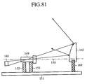
- FIG. 82 is a diagram depicting the configuration of a convex mirror for use in the image display device according to a 20th embodiment of the present invention.
- FIG. 86 is a diagram how optical system components are sequentially arranged by the alignment-adjusting method
- FIG. 87 is a diagram how optical system components are sequentially arranged by the alignment-adjusting method
- FIG. 88 is a diagram how optical system components are sequentially arranged by the alignment-adjusting method
- FIG. 90 is a diagram showing appearance of the image display device of each embodiment housed in a conventional cabinet
- FIG. 91 is a diagram showing appearance of a cabinet for the image display device according to a 22nd embodiment of the present invention.
- FIG. 92 is a diagram showing the case where two image display devices are assembled into a one-piece structure
- FIG. 94 is a diagram showing the case where four image display devices assembled into a one-piece structure
- FIG. 96 is a diagram showing the configuration of another conventional image display device using a plane mirror.
- FIG. 1 schematically illustrates the configuration of an image display device according to a first embodiment (Embodiment 1) of the present invention.
- Reference numeral 11 denotes a luminous element that emits light (illumination light); 12 denotes a parabolic reflector for reflecting the light from the luminous element 11 mostly into parallel rays of light; and 13 denotes a condenser lens for gathering the rays of light reflected by the parabolic reflector 12 .
- the luminous element 11 , the parabolic reflector 12 and the condenser lens 13 constitute a illumination light source system (sending means, illumination light source part).
- Reference numeral 14 denotes a micro-mirror device (sending means, a reflecting image information imparting part, digital micro-mirror device (DMD), a registered trademark of Texas Instruments Incorporated (TI)) that is a reflecting spatial light modulator.
- the micro-mirror device 14 spatially intensity-modulates the light gathered by the condenser lens 13 and reflects intensity-modulated light as an optical image signal containing image information. While the present invention is applicable to image display devices equipped with any kinds of spatial light modulators, the invention will hereinafter be described to use the micro-mirror device 14 .
- the reflecting surface of the micro-mirror device 14 and the light receiving surface of the screen 18 are disposed in parallel to minimize the depth dimension of the image display device. And, in order to prevent shading of light, the micro-mirror device 14 and the screen 18 are displaced from each other in the vertical direction, that is, they are staggered. Further, the projecting optical system 17 is so placed as to satisfy the above-mentioned positional relationship between the micro-mirror device 14 and the screen 18 and maintain the conjugate relationship between the image of the micro-mirror device 14 and the image on the screen 18 .
- the light emanating from the luminous element 11 is reflected by the parabolic reflector 12 , and impinges aslant on the reflecting surface of the micro-mirror device 14 through the condenser lens 13 .
- the micro-mirror device 14 spatially intensity-modulates the incident light based on image information.
- the thus intensity-modulated light is projected by the projecting optical system 17 onto the screen 18 to display thereon an image.
- the user of the image display device visually identifies the image from the left-hand side of the screen 18 in FIG. 1 .
- micro-mirror device 14 A description will be given of the micro-mirror device 14 .
- the micro-mirror device 14 has a reflecting surface formed by a two-dimensional arrays of 16 ⁇ m square micro mirrors with a 17 ⁇ m pitch, and the small mirrors usually have a one-to-one correspondence with image formats. For example, by a voltage from a controller (not shown), it is possible to change the inclination of each micro mirror and hence change the direction of light that is reflected off the micro mirror.
- the inclination of the micro mirror concerned is changed so that it reflects light toward the aperture of the projecting optical system 17 .
- the inclination of the micro mirror concerned is controlled so that light is reflected to the outside of the aperture of the projecting optical system 17 . Since the time for changing the inclination of each micro mirror is less than 10 ⁇ sec, the micro-mirror device 14 is capable of intensity modulating light at high speed.
- the micro-mirror device 14 is a reflecting type spatial light modulator, it is capable of intensity-modulating light incident thereon obliquely to its reflecting surface.
- the micro-mirror device 14 it is possible to dispose the illumination light source between the spatial light modulator and the convex mirror 16 on the side to which the micro-mirror device 14 emits light. This allows effective use of the space in the direction of the height of the image display device, preventing the illumination light source system from jutting out.
- the light intensity-modulated by the micro-mirror device 14 is reflected to the projecting optical system 17 .
- the optical axis of the refracting optical lens 15 is perpendicular to the reflecting surface of the micro-mirror device 14 and the light receiving surface of the screen 18 and is set off the center of the micro-mirror device 14 and the center of the screen 18 . Accordingly, only one part of the field angle of the refracting optical lens 15 is used to project the light from the micro-mirror device 14 . In FIG. 1, since the light is incident on the refracting optical lens 15 diagonally from below, the light is emitted diagonally upward.
- FIG. 2 is a diagram for conceptually explaining how a barrel distortion of the refracting optical lens 15 compensates for a pincushion distortion of the convex mirror 16 .
- the refracting optical lens 15 is so designed as to have a barrel distortion.
- FIG. 2 ( a ) When light of a grid-like image (FIG. 2 ( a )) is projected onto the refracting optical lens 15 from the micro-mirror device 14 , the grid-like image is transformed to a barrel shape (FIG. 2 ( b )).
- This barrel distortion is a feature of correcting for the pincushion distortion (FIG. 2 ( c )) that occurs in the convex mirror 16 .
- the refracting optical lens 15 is designed based on the pincushion distortion of the convex mirror 16 .
- FIG. 3 is a diagram conceptually showing how to calculate, by ray tracing, an image when the light from the micro-mirror device 14 is reflected by the convex mirror 16 or plane mirror 21 through an aplanatic refracting optical lens 19 .
- the solid lines indicate the optical path reflected by the plane mirror 21 and the broken lines the optical path reflected by the convex mirror.
- micro-mirror device 14 emits light having a grid-like image (FIG. 3 ( a )
- the light having passed through the aplanatic refracting optical lens 19 is not distorted (FIG. 3 ( b )).
- black dots are found to be arranged at equal intervals on a plane A-A′ perpendicular to the optical axis 20 of the refracting optical lens 19 (FIG. 3 ( d )). That is, in the case of the projecting optical system composed of the aplanatic refracting optical lens 19 and the plane mirror 21 , the grid-like image undergoes no distortion while remaining intact.
- pincushion distortion occurs on the plane A-A′ as indicated by white dots (FIG. 3 ( c )) because the position of reflection on the reflecting surface of the convex mirror 16 in the direction of its optical axis differs for each optical path. Since the pincushion distortion can be calculated by ray tracing once the shape of the convex mirror 16 is determined, the calculation result can be used to design the distortion of the refracting optical lens 15 in FIG. 1 .
- the refracting optical lens 15 is used to provide the barrel distortion that compensates for the pincushion distortion of the convex mirror 16 as described above, it is possible to display a magnified distortion-free image on the screen 18 placed at such a position as to provide a flat device configuration.
- the convex mirror 16 can easily be manufactured through mirror-finish lathing by forming its reflecting surface as a rotational aspherical surface that is obtainable by rotating a quadratic curve about an axis—this permits substantial reduction of the manufacturing costs.
- the convex mirror 16 can be designed freely according to the specifications of the image display device, and at any rate the refracting optical lens 15 needs only to be designed which has the barrel distortion that compensates for the pincushion distortion of the convex mirror 16 .
- the prior art requires such optical path bending means as the plane mirror 7 in FIG. 96 in addition to the projecting optical system 17 , but in this embodiment part of the projecting optical system functions to bend the optical path—this decreases the number of optical parts used and hence reduces the distance between the screen 18 and the convex mirror 16 accordingly.
- a plane mirror 22 for reflecting the light from the projecting optical system 17 is added to bend the optical path to the screen 18 , by which it is possible to make utmost use of the space of the image display device.
- the plane mirror 22 and the projecting optical system 17 may be interchanged, and the plane mirror 22 may be replaced with a projecting optical system other than that 17 .
- the image display device comprises: sending means composed of the illumination light source system and the micro-mirror device 14 , for emitting an optical image signal intensity-modulated based on image information; the screen 18 for receiving the optical image signal and displaying an image based on the image information; the convex mirror 16 having a negative power, for reflecting the intensity-modulated light onto the screen 18 ; and the refracting optical lens 15 having the barrel distortion that compensates for the pincushion distortion of the convex mirror 16 and so disposed as to project the light from the sending means onto the convex mirror 16 . It is therefore possible to compensate for the pincushion distortion of the intensity-modulated light by the convex mirror 16 and provide an enlarged display of the image on the screen 18 . And the screen 18 can be placed at the position optimal for reduction of the depth dimension of the image display device. Accordingly, the image display device according to this embodiment is smaller in its depth dimension than the prior art.
- the sending means is formed by the illumination light source composed of the luminous element 11 , the parabolic reflector 12 and the condenser lens 13 and the micro-mirror device 14 for modulating the light from the illumination light source system based on image information and reflecting the light
- the illumination light source system can be disposed at the side to which the micro-mirror device 14 reflects the intensity-modulated light. This also permits further reduction of the depth dimension of the device.
- the convex mirror 16 since the convex mirror 16 has a rotational aspherical surface, it can easily be manufactured by mirror-finish lathing—this permits substantial reduction of manufacturing costs.
- this embodiment forms the projecting optical system by a Fresnel mirror capable of magnifying an image with a short projection distance as is the case with the convex mirror and having no distortion.
- FIG. 5 is a diagram schematically depicting the configuration of an image display device according to Embodiment 2.
- Reference numeral 23 denotes an aplanatic refracting lens (a refracting optical part); 24 denotes a Fresnel mirror (a reflecting part) for reflecting light from the refracting optical lens 23 onto the screen 18 ; and 25 denotes a projecting optical system (projecting optical means) composed of the refracting optical lens 23 and the Fresnel mirror 24 .
- the reflecting surface of the Fresnel mirror 24 has negative power. For brevity sake, no illumination light source system is shown.
- FIG. 6 is a magnified view of the Fresnel mirror 24 .
- the convex mirror 16 in Embodiment 1.
- the reflecting surface of the Fresnel mirror has a periodic structure whose sections are identical in inclination with the corresponding sections of the reflecting surface of the convex mirror 16 .
- the Fresnel mirror 24 is thinner than the convex mirror 16 .
- FIG. 7 is a diagram for explaining the difference in distortion between the convex mirror 16 and the Fresnel mirror 24 .
- the optical paths in which a grid-like image (FIG. 7 ( a )) from the micro-mirror device 14 or aplanatic refracting optical lens 23 is reflected by the convex mirror 16 undergo pincushion distortion (FIG. 7, white dots) on the plane A-A′ perpendicular to the optical axis 27 of the refracting optical lens 23 due to a different position of reflection in each optical path that is attributable to the convex reflecting surface configuration.
- pincushion distortion FIG. 7, white dots
- the projecting optical system is made up of the Fresnel mirror 24 that magnifies an image with a short distance as is the case with the convex mirror but does not distort the image of light passing therethrough and the aplanatic refracting optical lens 23 , it is possible to display a magnified image on the screen 18 without the need for compensating the pincushion distortion of the convex mirror 16 by the refracting optical lens as in Embodiment 1—this facilitates the design and fabrication of the image display device.
- this embodiment uses, as part of the projecting optical system 2 , the Fresnel mirror 24 formed thinner than the convex mirror 16 , and hence permits further reduction of the depth dimension of the image display device.
- FIG. 8 is a diagram schematically illustrating the configuration of an image display device according to a third embodiment (Embodiment 3) of the present invention.
- Reference numeral 28 denotes a refracting optical lens (a refracting optical part); 29 denotes an optical element (a reflecting part) formed of two optical materials of different dispersion characteristics; and 30 denotes a projecting optical system (projecting optical means) made up of the refracting optical lens 28 and the optical element 29 .
- a projecting optical system projecting optical means
- FIG. 9 depicts the optical element in enlarged dimension.
- Reference numerals 31 and 33 denote low dispersion glass (low dispersion medium) and high dispersion glass (high dispersion medium), respectively; 32 denotes an interface between the low dispersion glass 31 and the high dispersion glass 33 ; and 34 a reflecting surface that forms an interface between the high dispersion glass 33 and air.
- the interface 32 has a concave configuration that provides positive power and the reflecting surface 34 has a convex configuration that provides negative power.
- FIG. 10 is a diagram showing the optical path of incident light in the optical element 29 .
- the left-hand side of the interface 32 corresponds to the low dispersion glass 31 (of a refractive index n 1 ) and the right-hand side corresponds to the high dispersion glass 33 (of a refractive index n 2 ).
- the refractive indexes n 1 and n 2 can be chosen arbitrarily, but in this example n 1 ⁇ n 2 .
- a convex mirror which has the same configuration as that of the reflecting surface 34 , used, and the optical path of the incident light merely bent by the convex mirror used as the reflecting surface 34 is indicated by the broken lines.
- the optical path by the optical element 29 which passes through the low dispersion glass 31 and the high dispersion glass 33 in this order and strikes on the convex reflecting surface 34 , can be bend at an angle larger than in the case of the optical path bend by the mere convex mirror, and consequently a wider-angle image can be projected onto the screen 18 .
- the optical element 29 With the use of the optical element 29 , it is possible to project an image onto the screen 18 at wider angle than does the reflecting surface 16 in Embodiment 1 and hence reduce the convexity of the reflecting surface 34 accordingly. Further, since the position of emission of light from the optical element 29 can be controlled by adjusting the thicknesses of the low dispersion glass 31 and the high dispersion glass 33 , the distortion that occurs in the reflecting surface 34 can be compensated inside the optical element 29 .
- FIG. 11 there are indicated optical paths of red and blue colors by the solid and broken lines, respectively.
- Glass is called high or low dispersion glass, depending on whether its refractive index changes greatly with a change in the wavelength of incident light.
- glass materials have a characteristic that the refractive index increases with a decrease in the wavelength of light.
- the blue light of shorter wavelength is greatly refracted in the low dispersion glass, whereas the red light of longer wavelength is not so refracted as is the blue light.
- the high dispersion glass 33 differs from the low dispersion glass 31 in terms of the degree of refraction according to color, it is possible, even with a high dispersion glass of lower power than that of the low dispersion glass 31 , to provide dispersion with which color aberration having occurred in the low dispersion glass 31 can be compensated for.
- an achromatic lens of positive power can be constituted by such a combination of high and low dispersion glass materials.
- An achromatic lens of negative power can be obtained simply by reversing the combination of the low dispersion glass 31 and the high dispersion glass 33 .
- the low dispersion glass 31 is disposed on the light receiving side, but an optical element 35 of such a structure as shown in FIG. 12, in which a low dispersion glass 38 is sandwiched between a high dispersion glass 36 disposed at the light receiving side and a reflecting surface 39 of negative power, may sometimes be more effective in achromatization.
- Such optical element structures can be freely chosen at the time of design.
- light is projected onto the screen 18 by the optical element 29 that is composed of the low dispersion glass 31 and the high dispersion glass 33 laminated in the direction of transmission of light and the reflecting surface that has negative power and reflects the light having passed through the low dispersion glass 31 and the high dispersion glass 33 .
- This embodiment corrects for distortion by a refracting lens or convex mirror that has a aspherical refracting or reflecting surface.
- the aspherical lens 42 is disposed between the refracting optical lens 40 and the spherical convex mirror 43 at the position where the principal rays are divergent, and the light from the micro-mirror device 14 , which passes through the refracting optical lens 40 and the aspherical lens 42 , is reflected by the spherical convex mirror 43 for projection onto the screen 18 .
- the reflecting surface configuration of the aspherical convex mirror 41 or the refracting surface configuration of the aspherical lens 42 has a one-to-one correspondence with the distortion, the reflecting surface configuration or refracting surface configuration is designed through ray tracing in either case.
- the aspherical lens 42 and the aspherical convex mirror 41 could be placed as depicted in FIG. 13 ( c ). This arrangement allows more ease in correcting for distortion.
- aspherical lens 42 can be interposed between the refracting optical lens 40 and the aspherical convex mirror 41 (or the spherical convex mirror 43 ), in which case distortion can be further corrected for.
- FIG. 14 depicts the configuration of an image display device according to this embodiment.
- Reference numeral 45 denotes an aspherical convex mirror (projecting optical means, a reflecting part) that has a reflecting surface whose convex curvature is large at the center of the optical axis but gradually decreases toward the periphery.
- the spherical convex mirror 43 (indicated by the broken line) and the reflected ray (indicated by the broken-line arrow) by the spherical convex mirror 43 .
- the pincushion distortion occurs in the spherical mirror 43 and causes distortion of an image. Since the pincushion distortion appears in the periphery of the spherical convex mirror 43 , the illustrated example uses the aspherical convex mirror 45 having a reflecting surface whose convex curvature is large at the center of the optical axis 44 but gradually diminishes toward the periphery. The use of such an aspherical convex mirror permits further reduction of distortion.
- FIG. 15 depicts another configuration of the image display device according to this embodiment. Neither the illumination light source system nor the screen is shown for brevity sake.
- Reference numeral 46 denotes an aspherical convex mirror (projecting optical means, a reflecting part) that has an odd-order aspherical reflecting surface.
- a three-dimensional curved surface is expressed by a polynomial composed of even-order terms.
- the odd-order aspherical reflecting surface of the aspherical convex mirror 46 in FIG. 15 is obtained. It will be seen from FIG. 15 that, in comparison with the aspherical reflecting surface of the aspherical convex mirror 45 (indicated by the broken line), the odd-order aspherical reflecting surface of the aspherical convex mirror 46 has a convexity (or concavity) in the vicinity of the optical axis 44 .
- the convexity (or concavity) near the optical axis 44 is formed by adding odd-order terms to the polynomial.
- the micro-mirror device 14 When the micro-mirror device 14 is placed off the optical axis 44 as depicted in FIG. 15, the reflecting surface near the optical axis 44 does not project light. Accordingly, even if the projection and image formation performance near the optical axis is deteriorated by discontinuity of the curvature of the central area of the aspherical convex mirror 46 , no influence is exerted to the display performance of the display device.
- the use of the aspherical convex mirror 46 implements a projecting optical system in which the correction for distortion is consistent with an excellent image formation characteristic for off-axis projected light.
- the odd-order aspherical surface is also applicable to the refracting optical lens.
- At least one aspherical lens 42 having an aspherical refracting surface is interposed between the refracting optical lens 40 and the convex mirror at the position where the principal ray is disturbed, it is possible to correct for distortion of the light that is projected onto the screen 18 .
- the aspherical convex mirror 45 is used whose convex curvature is large at the center of the optical axis but gradually decreases toward the periphery, the light to be projected onto the screen 18 can be further corrected for distortion.
- the aspherical convex mirror 46 which has an odd-order aspherical reflecting surface formed by adding an odd-order term to a polynomial representing an even-order aspherical surface, it is possible to implement a projecting optical system in which the correction for distortion and an excellent image formation performance for off-axis projected light are compatible with each other.
- the aspherical lens 47 which as an odd-order aspherical refracting surface formed by adding an odd-order term to a polynomial representing an even-order aspherical surface, it is possible to locally modify the configuration of the refracting surface, facilitating reduction of distortion and permitting improvement in the off-axis image formation performance.
- some of lenses forming the refracting optical part can be mass-produced with a die of a desired aspherical configuration by injection molding of plastic synthetic resin such as polycarbonate or acrylic plastic.
- plastic synthetic resin such as polycarbonate or acrylic plastic.
- the melting point of glass for use as a material for a lens is about 700° C. and the melting point of glass for molding use is 500° C., whereas the melting point of the plastic synthetic resin is lower; hence, the fabrication of the refractive optical lens from the plastic synthetic resin provides increased productivity, and cuts the manufacturing cost of the image display device.
- the aspherical lenses 42 and 47 can be obtained by a known glass molding method.
- environmental characteristics such as the operating temperature range and humidity range
- the lens material for the refracting optical part needs only to be chosen according to the purpose, usage and specifications of the image display device desired to fabricate, taking into account merits of individual materials.
- Embodiment 4 is adapted to correct for distortion by means of the aspherical convex mirror having an aspherical reflecting surface or refracting optical lens having an aspherical refracting surface as described above, but in this case a curvature of field occurs in the image projected onto the screen 18 , developing what is called an “out of focus” phenomenon.
- a fifth embodiment (Embodiment 5) of the present invention is intended to reduce the curvature of field.
- ⁇ is an operator that means the sum total related to an index i of sum
- i is the number of an optical element
- N is the total sum of optical elements
- Pi is a component of an i-th optical element that contributes to the Petzval's sum
- ni is the refractive index of the i-th optical element
- fi is the focal length of the i-th optical element
- ⁇ i represents the power that the i-th optical element has.
- the refracting optical lens 48 is an achromatic lens 48 composed of a positive lens 48 A and a negative lens 48 B.
- the component P3 of the aspherical convex mirror 41 that contributes to the Petzval's sum P is likely to take a positive value owing to a division of negative values.
- the contributing component P1+P2 is made to approach the negative value as much as possible, thereby reducing the influence of the component P1+P2 on the component P3 of the aspherical convex mirror 41 .
- the Petzval's condition can be further satisfied by setting Abbe's numbers ⁇ 1 and ⁇ 2 of the positive and negative lenses 48 A and 48 B to values close to each other.
- FIG. 18 there are shown variations in the absolute values of ( ⁇ 1 ⁇ ) and ( ⁇ 2/ ⁇ ) for ( ⁇ 2/ ⁇ 1) when Equations (2) and (3) are modified to the following Equations (4) and (5), respectively.
- the abscissa represent ( ⁇ 2/ ⁇ 1) and the ordinate represents absolute values of Equations (4) and (5),
- the Abbe's numbers ⁇ 1 and ⁇ 2 of the positive and negative lenses 48 A and 48 B are set to values close to each other by increasing the refractive index n1 of the positive lens 48 A and decreasing the refractive index n2 of the negative lens 48 B.
- the refractive index of the positive lens 48 A is increased and the refractive index of the negative lens 48 B is decreased so that the Petzval's condition is approached from the above state.
- the Abbe's numbers ⁇ 1 and ⁇ 2 of the positive and negative lenses 48 A and 48 B are set to values close to each other.
- this embodiment uses the refracting optical lens 48 composed of the positive lens 48 A of positive power and the negative lens 48 B of negative power, the refracting index of the former being made larger than the refractive index of the latter and their Abbe's numbers being set to values close to each other.
- a refracting optical lens 48 it is possible to correct for distortion and satisfy the Petzval's condition to correct for the curvature of field.
- a sixth embodiment (Embodiment 6) of the present invention generates an over curvature of field by a refracting optical lens to correct for the curvature of field that occurs in the aspherical convex mirror.
- FIG. 19 is explanatory of an under curvature of field that occurs in the aspherical convex mirror.
- reference numeral 49 denotes a refracting optical lens
- 50 denotes the optical axis of the refracting optical lens 49
- 51 denotes a plane perpendicular to the optical axis 50 .
- Light having passed through the refracting optical lens 49 forms an image on the plane 51 .
- FIG. 19 ( a ) a flat image is obtained.
- the refracting optical system is used to provide an over curvature of field to flatten the projected image surface.
- an image surface 53 having an over curvature of field such that the focal length increases with distance from the optical axis 44 is provided by a refracting optical lens (projecting optical means, a refracting optical part, a curvature of field correcting lens) 54 interposed between the micro-mirror device 14 and the aspherical convex mirror 41 , thereby canceling the over curvature of field by the refracting optical lens 54 and the under curvature of field by the aspherical convex mirror 41 .
- a refracting optical lens projecting optical means, a refracting optical part, a curvature of field correcting lens
- the configuration of the refracting surface of the reracting optical lens 54 can be optimized through numerical calculations for ray tracing by a computer.
- FIG. 21 shows the results of numerical calculations for ray tracing.
- An aspherical lens (projecting optical means, a refracting optical part, an aspherical optical element) 55 is placed at the position where the rays from the micro-mirror device 14 (not shown) are convergent
- aspherical lenses (projecting optical means, a refracting optical part, aspherical optical elements) 56 A and 56 B are placed at the position where rays from the asperical lens 55 diverge
- an aspherical convex mirror (projecting optical means, a reflecting part, an aspherical optical element) 57 is placed at the position where rays from the aspherical lens 56 B diverge; the light reflected by the aspherical convex mirror 57 is projected onto the screen 18 .
- the aspherical lens 55 effectively reduces curvature of field
- the aspherical lenses 56 A and 56 B and the aspherical convex mirror 57 effectively reduce distortion.
- FIG. 22 is a table showing, by way of example, the results of numerical calculations in FIG. 21 .
- the aspherical surfaces used in FIG. 22 are defined by the Equations (6) and (7) given below, where z is the amount of sag from a tangent plane passing through the center of rotation of an optical plane, c the curvature at a surface apex (an inverse of the radius of curvature), k is a conic coefficient and r is the distance from the z axis.
- Equations (6) and (7) given below, where z is the amount of sag from a tangent plane passing through the center of rotation of an optical plane, c the curvature at a surface apex (an inverse of the radius of curvature), k is a conic coefficient and r is the distance from the z axis.
- this embodiment uses the refracting optical lens 54 to provide the over curvature of field that cancels the under curvature of field by the aspherical convex mirror 41 ; hence, it is possible to display an image corrected for curvature of field as well as distortion.
- this embodiment effectively reduces curvature of field at the position where principal rays are convergent and distortion at the position where the principal rays are divergent, by placing aspherical optical elements at such positions, respectively.
- the refracting optical lens 54 may be applied as well to the other asphericl convex mirrors in Embodiment 4.
- FIGS. 23 ( a ), ( b ) and ( c ) are front, top plan and side views of an image display device according to a seventh embodiment (Embodiment 7) of the present invention.
- Reference numeral 58 denotes a refracting optical lens (projecting optical means, a refracting optical part) that transmits light from the micro-mirror device 14 and corresponds to the refracting optical lens described in respect of the embodiments described above.
- Reference numeral 59 denotes an path-bending reflector (optical path bending means) for reflecting the light from the refracting optical lens 58 ;
- 60 a convex mirror of negative power (projecting optical means, a reflecting part), which is the same convex mirror as those described in the preceding embodiments;
- 61 denotes the optical axis of the convex mirror 60 .
- no illumination light source is shown.
- the refractive optical lens 58 and the convex mirror 60 are common in optical axis.
- the path-bending reflector 59 is used to bend the optical axis through an appropriate angle in the horizontal plane containing the optical axis 61 of the convex mirror 60 .
- the optical axis of the refracting optical lens 58 initially coincident with the optical axis of the convex mirror 60 , it turned about the normal to the horizontal plane containing the optical axis 61 of the convex mirror 60 until a proper azimuth is reached. In this way, the refracting optical lens 58 is placed in an empty space of the image display device.
- the light from the micro-mirror device 14 having passed through the refracting optical lens 58 , is reflected first by the path-bending reflector 59 toward the convex mirror 60 , and the light reflected by the convex mirror 60 is reflected by the plane mirror 22 referred to previously with respect to Embodiment 1, thereby performing a wide-angle projection onto the screen 18 .
- the parallel arrangement of the reflecting surface of the plane mirror 22 and the light receiving surface (or an image display surface) of the screen 18 minimizes the depth dimension of the image display device.
- the point of this embodiment lies in an arrangement in which the light from the refracting optical lens 58 placed in an empty space of the image display device is reflected by the path-bending reflector 59 to the convex mirror 60 . Since the refracting optical lens 58 and an illumination light source system (not shown) can be disposed in the empty space, the depth dimension of the image display device can be reduced.
- the path-bending reflector 59 is provided, but since the optical axis of the refracting optical lens 58 is bent in a plane other than the horizontal plane containing the optical axis of the convex mirror 60 , it is necessary that the refracting optical lens 58 , the micro-mirror device 14 and the illumination light source system (not shown) be disposed below the convex mirror 60 , inevitably making the height of the under-the-screen portion larger than in the image display device of FIG. 23 .
- the path-bending reflector in a refracting optical lens (projecting optical means, a refracting optical part) composed of a plurality of lenses, though not shown. That is, the path-bending reflector is inserted between first and second lens means forming the refracting optical lens so that the path-bending reflector transmits the light between the two lenses through reflection.
- the first and second lens means are each formed by at least one refracting optical lens.
- the refracting optical lens can be formed by bending two optical axes. This also reduces the depth dimension of the image display device as in the case of FIG. 23 .
- a plurality of path-bending reflectors can be used according to the number of lenses used.
- an path-bending reflector for reflecting light from the refracting optical lens to the convex mirror and an path-bending reflector for reflecting light from an arbitrary lens of the refracting optical lens to a different lens may be combined; this can be designed according to the specifications of the image display device.
- the refracting optical lens 58 and the illumination light source system can be disposed in the empty space of the image display device.
- the depth dimension of the image display device can be further decreased and the height of the part under the screen can be made small.
- the refracting optical lens can be formed by bending the optical axes of the first and second lens means. Hence, the depth dimension of the image display device can be further reduced and the height of the under-the-screen portion can be made small.
- this embodiment is applicable to Embodiments 1 to 6.
- the optimum optical system configuration for attaining the objective of the present invention can be obtained concretely through numerical calculations for ray tracing by a computer.
- FIG. 26 is a diagram illustrating the configuration of an image display device according to an eighth embodiment (Embodiment 8) of the present invention, which utilizes the numerical values (numerical value example 6A) shown in FIG. 21 .
- Reference numeral 14 denotes a micro-mirror device; 62 denotes a retro-focus optical system (projecting optical means, a refracting optical part) formed by positive lenses of positive power and negative lenses of negative power; 63 denotes a refracting optical lens (projecting optical means, a refracting optical part) for making fine adjustments to the angle of emission of light; and 64 denotes an aspherical convex mirror (projecting optical means, a reflecting part) for reflecting the light from the refracting optical lens 63 to correct for distortion.
- the illumination light source part and the screen are not shown.
- the light from the micro-mirror device 14 passes through the retro-focus optical system 62 and is transmitted by the refracting optical lens 63 to the convex mirror 64 , thereafter being projected onto the screen (no shown).
- the retro-focus optical system 62 has light-gathering power and, at the same time, assists widening of the field angle of the ray to be projected onto the screen.
- the refracting optical lens 63 corrects for the distortion uncorrected for by the aspherical convex mirror 64 .
- the retro-focus optical system 62 and the refracting optical lens 63 include the various refracting optical lenses referred to in the embodiments described previously.
- the retro-focus optical system 62 is composed of two positive lens groups 62 A and 62 B and one negative lens group 62 C as depicted in FIG. 27 ( a ), two positive lens groups 62 D and 62 E and one negative lens group 62 F as depicted in FIG. 27 ( b ), or one positive lens group 62 G and one negative lens group 62 H as depicted in FIG. 27 ( c ).
- FIGS. 28 and 29 are a table showing numerical data of Numerical Value Example 8A and the device configuration based on the numerical data, respectively.
- FIG. 29 corresponds to FIG. 27 ( a ).
- the positive lens group 62 B is an achromatic lens composed of positive and negative lenses.
- FIGS. 30 and 31 are a table showing numerical data of Numerical Value Example 8B and the device configuration based on the numerical data, respectively.
- FIG. 31 corresponds to FIG. 27 ( b ).
- the positive lens group 62 E is formed by one lens.
- FIGS. 32 and 33 are a table showing numerical data of Numerical Value Example 8C and the device configuration based on the numerical data, respectively.
- FIG. 33 corresponds to FIG. 27 ( c ).
- FIGS. 34 to 37 show Numerical Value Examples 4A and 4B related to Embodiment 4
- FIGS. 38 and 39 show Numerical Value Example 7A related to Embodiment 7.
- FIGS. 34 and 35 are a table showing numerical data of Numerical Value Example 4A and the device configuration based on the numerical data, respectively.
- FIGS. 36 and 37 are a table showing numerical data of Numerical Value Example 4B and the device configuration based on the numerical data, respectively. Either of them corresponds to Embodiment 4, in which that one of the two aspherical lenses 47 near the asphericl convex mirror 46 is made of acrylic resin and the other aspherical lens on the side opposite the aspherical convex mirror 46 is made of polycarbonate.
- the temperature coefficients of refractive index and coefficient of linear expansion of plastic materials are two orders of magnitude greater than those of glass. Accordingly, special consideration must be given to the usage when they are used in an environment of large temperature variations.
- the two aspherical lenses 47 have their central and peripheral portions formed substantially equal in thickness with a view to reducing the influence of a temperature change on the configuration of the aspherical lenses 47 .
- FIGS. 38 and 39 are a table showing numerical data of Numerical Value Example 7A and the device configuration based on the numerical data, respectively.
- This example corresponds to Embodiment 7 and is intended to reduce the depth dimension of the display device by placing the path-bending mirror at the position indicated by the broken line.
- the average value, ave_Nn, of refractive index of the negative lenses and the average value, ave_Np, of refractive indexes of the positive lenses are 1.45 ⁇ ave_Nn ⁇ 1.722 and 1.722 ⁇ ave_Np ⁇ 1.9, respectively.
- the average value, ave_ ⁇ dn, of Abbe's number of the negative lenses and the average value, ave_ ⁇ dp, of Abbe's number of the positive lenses are 25 ⁇ ave_ ⁇ dn ⁇ 38 and 38 ⁇ ave_ ⁇ dp ⁇ 60, respectively.
- dif_ave_N The difference, dif_ave_N, between the average values of the refractive indexes of glass materials for the positive lenses and the negative lenses is 0.04 ⁇ dif_ave_N ⁇ 1.
- dif_ave_ ⁇ d The difference, dif_ave_ ⁇ d, between the average values of the Abbe's number of the glass materials for the positive and negative lenses is 0 ⁇ dif_ave_ ⁇ d ⁇ 16.
- Features 1 and 2 correspond to the case where the refractive index of the positive lens 48 A and the refractive index of the negative lens 48 B, which form the refracting optical lens 48 (a Petzval's sum correcting lens) in Embodiment 5, are set high and low, respectively.
- materials of Abbe's number in the range of 70 to 90 are also commonly used for achromaticity use, but in the present invention the Abbe's number of the material used is smaller than 60 as will be seen from Feature 2.
- this embodiment employs the FIG. 26 configuration.
- the back focal length (BFL) which is the distance from micro-mirror device 14 to the lens nearest it, and the distance from the micro-mirror device 14 to the position of an entrance pupil of the retro-focus optical system 62 are chosen to be equal to each other. This minimizes the shading of light, illuminating the screen with increased efficiency. The reason for this will be described below.
- the distance from the micro-mirror device 14 to the position of entrance pupil is set to be equal to the back focal length—this minimizes the diameter of the refracting optical lens and suppresses shading of light, providing increased illumination efficiency. It is a matter of course to apply the above-described shading minimization scheme to the other embodiments as well.
- the position of entrance pupil and the back focal length are virtually coincident; complete coincidence of them will provide the best results.
- this embodiment uses the retro-focus optical system 62 composed of positive and negative lens groups, the refracting optical lens 63 for making fine adjustments to the angle of emission of light and the aspherical convex mirror 64 for correcting for distortion, it is possible to suppress distortion and curvature of field, permitting reduction of the depth dimension of the image display device.
- the retro-focus optical system 62 is made up of the positive lens group 62 A ( 62 D), the positive lens group 62 B ( 62 E) and the negative lens group 62 C ( 62 F)—this also suppresses distortion and curvature of field, permitting reduction of the depth dimension of the image display device.
- the retro-focus optical system 62 is made up of the positive lens group 62 G and the negative lens group 62 H—this also suppresses distortion and curvature of field, permitting reduction of the depth dimension of the image display device.
- the average refractive indexes of the negative and positive lenses are set in the ranges of from 1.45 to 1.722 and from 1.722 to 1.9, respectively. This also suppresses distortion and curvature of field, permitting reduction of the depth dimension of the image display device.
- the average Abbe's number of the glass materials for the negative and positive lenses are set in the ranges of from 25 to 38 and from 38 to 60, respectively. This also suppresses distortion and curvature of field, permitting reduction of the depth dimension of the image display device.
- the average refractive indexes of the glass materials for the positive and negative lenses of the refracting optical lens are chosen such that their difference is in the range of from 0.04 to 1. This also suppresses distortion and curvature of field, permitting reduction of the depth dimension of the image display device.
- the average Abbe's number of the glass materials for the positive and negative lenses of the refracting optical lens are chosen such that their difference is in the range of from 0 to 16. This also suppresses distortion and curvature of field, permitting reduction of the depth dimension of the image display device.
- the back focal length from the micro-mirror device 14 to the refracting optical lens nearest it and the distance from the micro-mirror device 14 to the position of entrance pupil of the retro-focus optical system 62 are set to coincide with each other. This minimizes the diameter of the refracting optical lens and minimizes the shading of light, providing for increased illumination efficiency.
- This embodiment (Embodiment 9) is intended to meet the Petzval's condition by a negative lens that is interposed between the micro-mirror device and a reflector at a position where the marginal ray is low.
- FIG. 41 illustrates the configuration of an image display device according to this embodiment, (a) showing its whole structure and (b) its partially enlarged view.
- the illumination light source, the micro-mirror device and the screen are not shown.
- Reference numerals 67 and 68 denote refracting optical lenses; 69 denotes a convex mirror that has a positive Petzval's sum contributing component; 70 denotes an optical axis common to the refracting optical lenses 67 and 68 and the convex mirror 69 ; 71 denotes a marginal ray of light traveling from the micro-mirror device (not shown) to the convex mirror 69 ; and 72 denotes a negative lens disposed at the position where the marginal ray is low.
- the convex mirror 69 has a positive Petzval's sum contributing component
- the Petzval's sum of the whole projecting optical system made up of the refracting optical lenses 67 and 68 and the convex mirror 69 readily goes positive, giving rise to a curvature of field.
- the negative lens 72 having a negative power of large absolute value is used to provide a negative Petzval's sum contributing component, which is utilized to reduce the Petzval's sum of the entire optical system to zero. This permits reduction of the curvature of field.
- the point of this embodiment is to place the negative lens 72 at the position where the marginal ray 71 is low. That is, in this embodiment the negative lens 72 is disposed between the micro-mirror device (not shown) and the convex mirror 69 at the position where the marginal ray 71 is low. At this position light converges on the optical axis 70 .
- the negative lens 72 may also be disposed in the retro-focus optical system 62 of Embodiment 6; furthermore, since the reflecting surface of the micro-mirror device (the light emitting surface in the case of a transmission spatial light modulator such as liquid crystal) corresponds to the position where the marginal ray 71 is low, a condenser lens (field flattener) may be placed as the negative lens 72 in proximity to the reflecting surface (the light emitting surface).
- a condenser lens field flattener
- the negative lens 72 is not limited specifically to a single-lens structure but may be of a multi-lens structure.
- the negative lens 72 is placed at he position where the marginal ray 71 is low, it is possible to easily satisfy the Petzval's condition by generating the negative Petzval's sum contributing component that cancels the positive Petzval's sum contributing component of the projecting optical system, without the need for considering the lens effect of the negative lens 72 on the light passing therethrough. Hence, the curvature of field can be reduced.
- Embodiment 7 minimizes the thickness or depth dimension of the image display device and the height of the under-the-screen portion of the device by the path-bending reflector 59 interposed between the refracting optical lens 58 and the convex mirror 60 to bend the optical path in the horizontal plane containing the optical axis 61 .
- This embodiment (Embodiment 10) is directed to the conditions for the arrangement of the path-bending reflector 59 and the refracting optical lens 58 relative to the convex mirror 60 in Embodiment 7.
- FIG. 42 is explanatory of the conditions for placement of the path-bending reflector 59 .
- FIGS. 42 ( a ) and 42 ( b ) are a side and a top plan view of the image display device, and
- FIG. 42 ( c ) is a front view of the convex mirror 60 .
- the parts identical to or corresponding to those in FIG. 23 are identified by the same reference numerals.
- FIG. 42 ( a ) and 42 ( b ) are a side and a top plan view of the image display device
- FIG. 42 ( c ) is a front view of the convex mirror 60 .
- the parts identical to or corresponding to those in FIG. 23 are identified by the same reference numerals.
- FIG. 42 is explanatory of the conditions for placement of the path-bending reflector 59 .
- FIGS. 42 ( a ) and 42 ( b ) are a side and a top plan view of the image display device
- reference numeral 73 denotes the optical axis of the refracting optical lens 58
- 58 z denotes the refracting optical lens 58 in the case where it is assumed that the optical bending mirror 59 is removed to bring the optical axis 61 of the convex mirror 60 and the optical axis 73 into alignment with each other.
- the optical axes 61 and 73 intersect at an angle ⁇ in the horizontal plane. That is, the optical axis 73 aligned with the optical axis 61 is turned through 180- ⁇ in the horizontal plane to intersect the optical axis 61 as depicted in FIG. 42 ( b ).
- Reference characters P and Q denotes two points on the line of intersection between the horizontal plane containing the optical axis 73 and the refracting optical lens 58 , the point P being a point that is the closest to the optical path from the path-bending reflector 59 to the convex mirror 60 and the point Q being a point that is the closest to the plane in the flat plane 22 is set.
- b represent the distance between the convex mirror placement plane (reflecting part placement plane) where the convex mirror 60 is disposed and the position of the path-bending reflector 59 , and let those of points on the line of intersection between the horizontal plane containing the optical axis 61 and the path-bending reflector 59 which are the closest to and the farthest from the convex mirror placement plane be called the closest point and the farthest points, respectively.
- Reference character a denotes the distance from the closest point to the convex mirror placement plane
- c denotes the distance from the farthest point to the convex mirror placement plane.
- the distance c is the longest distance from the convex mirror placement plane to the path-bending reflector 59 .
- Reference character m denotes the distance from the highest point of the path-bending reflector 59 to the optical axis 61 ; g denotes the distance from the point Q to the convex mirror placement plane; and f denotes the distance from the position of the exit pupil of the refracting optical lens 58 z to the convex mirror placement plane.
- the distance g is the longest distance from the convex mirror placement plane to the refracting optical lens 58 . Accordingly, the sum of the distance from the position of the exit pupil of the refracting optical lens 58 to the path-bending reflector 59 and the horizontal distance from the position of the path-bending reflector 59 to the convex mirror placement plane is equal to the distance f.
- the distance a is maximized to ensure the passage of the reflected ray from the convex mirror 60 along the lowest possible path.
- the distance c needs to be held smaller than the limit.
- the portion of the refracting optical lens containing the point P intercepts the reflected ray from the path-bending reflector 59 to the convex mirror 60 . If the refracting optical lens 58 is disposed so that its portion containing the point P will not intercept the reflected ray from the path-bending reflector 59 to the convex mirror 60 , the distance a becomes shorter than required. On the other hand, if the distance f is too long, the refracting optical lens 58 is spaced more than necessary from the path-bending reflector 59 owing to the conditions imposed on the positions of the light receiving surface of the convex mirror 60 and the reflector 59 . As a result, the path-bending reflector 59 becomes large and its height increases accordingly, intercepting the reflected ray 75 from the convex mirror 60 to the lowermost end of the screen 18 . To avoid this, the distance f has the optimum value.
- a decrease in the angle ⁇ decreases the distance g or c—this is advantageous from the viewpoint of the thickness of the refracting optical lens 58 or path-bending reflector 59 .
- the portion of the refracting optical lens 58 containing the point P projects into the optical path from the path-bending reflector 59 to the convex mirror 60 and intercepts the light, casting a shadow on the screen 18 .
- the angle ⁇ also has the optimum value.
- the path-bending angle ⁇ is determined such that the point P is as close to the optical path from the path-bending reflector 59 to the convex mirror 60 as possible within the range in which the point P does not intercept the reflected light.
- the distance f is determined so that the longer one of the distances g and c defines the depth dimension of the device. In particular, setting the distances c and g to the same value minimizes the height of the under-the-screen portion.
- the angle ⁇ may sometimes be predetermined according to other conditions of the image display device, but it can also be considered to the same as in the above.
- the angle ⁇ is set to such a value that the point P of the refracting optical lens 58 is as close to the optical path from the path-bending reflector 59 to the convex mirror 60 as possible within the range in which the point P does not intercept the optical path.
- the distance f is set to such a value that the point P of the refracting optical lens 58 is as close to the optical path from the path-bending reflector 59 to the convex mirror 60 as possible within the range in which the point P does not intercept the optical path and that the distance c or g defines the thickness or depth dimension of the device.
- the angle ⁇ is set to such a value that the point P of the refracting optical lens 58 is as close to the optical path from the path-bending reflector 59 to the convex mirror 60 as possible within the range in which the point P does not project into the optical path, while at the same time the distance f is set such that the distances c and g are equal to each other and defines the thickness or depth dimension of the device.
- the entire area of the reflecting surface of the convex mirror is not used to project light onto the screen, but the area of the reflecting surface for projecting the light is only one-half or less of the entire reflecting surface area. Accordingly, if such an unnecessary reflecting surface area (nonreflecting area) is removed as in the case of the convex mirror 60 shown in FIG. 42 ( c ), it is possible to downsize the convex mirror accordingly and hence cut the manufacturing cost of the image display device and permit effective use of the limited space inside the image display device. Further, two convex mirror, equally divided from one convex mirror obtained by rotational formation, can be used in two image display deices—this permits simplification of the manufacturing process of image display devices.
- FIG. 43 depicts a retaining mechanism 74 , which is used to hold the refracting optical lens 58 , the path-bending reflector 59 and the convex mirror 60 as one piece.
- the use of such a retaining mechanism 74 allows ease in accurately forming the optical path between the respective optical components with their positional relationships held as predetermined.
- the refracting optical lens 58 , the reflector 59 and the convex mirror 60 are mounted against dislocation by external stress or variations of various environmental conditions (temperature, humidity, etc.)—this stabilizes the performance of the image display device. It is a matter of course that when the path-bending reflector 59 is not used, only the refracting optical lens 58 and the convex mirror 60 can be held by the retaining mechanism.
- the thickness or depth dimension of the image display device can also be suppressed by placing the path-bending reflector between the first and second lens means of the refractive optical lens 58 as depicted in FIG. 44 instead of interposing the reflector 59 between the refracting optical lens 58 and the convex mirror 60 as mentioned previously with reference to Embodiment 7.
- FIG. 44 the parts identical with or corresponding to those in FIG. 42 are identified by the same reference numerals.
- the light from the micro-mirror device passes through the first lens means of the refracting optical lens 58 and is reflected by the path-bending reflector 59 , thereafter passing through the second lens means of the lens 58 and traveling to the convex mirror 60 .
- the distance g is the longest distance from the convex mirror placement plane to the refracting optical lens 58 .
- the refracting optical lens 58 be spaced as far apart from the convex mirror 60 as possible so that the optical path of the reflected ray 75 from the convex mirror 60 to the lowermost end of the screen 18 is as close to the optical axis 61 as possible.
- the refracting optical lens 58 intercepts the optical path of the reflected ray 75 if it is lower than the highest point R of the exit surface of the refracting optical lens 58 .
- the refracting optical lens 58 is disposed so that the shortest distance a between it and the convex mirror placement plane is as long as possible. Hence, in the case of FIG. 44, too, there is the optimum value for the distance f from the convex mirror placement plane to the exit pupil of the refracting optical lens 58 .
- the path-bending angle ⁇ needs to be minimized from the viewpoint of thickness reduction.
- the first lens means will intercept the optical path from the path-bending reflector to the second lens means. This indicates that there is the optimum value for the angle ⁇ in the case of FIG. 44, too.
- a prism may be used as a substitute for the path-bending reflector.
- FIG. 45 illustrates the configuration of an image display device according to an eleventh embodiment (Embodiment 11) of the present invention.
- the illumination optical part and the screen are not shown.
- the lens diameters of the light receiving and emitting sides of the refracting optical lens interposed between the micro-mirror device and the reflector are made smaller than the central lens diameter of the refracting optical lens to meet the Petzval's condition and establish an optical system advantageous for path-bending condition.
- reference numeral 14 denotes a micro-mirror device
- 76 denotes a refracting optical lens (refracting optical part)
- 77 denotes a convex mirror having a positive Petzval's sum contributing component
- 78 denotes an optical axis common to the refracting optical lens 76 and the convex mirror 77
- 79 denotes a marginal ray of light that travels from the micro-mirror device 14 to the convex mirror 77 .
- reference numeral 80 denotes a positive lens disposed at a position where the marginal ray 79 is high
- 81 and 82 denote lens groups disposed at the entrance and exit sides of the positive lens 80 , respectively.
- the light from the micro-mirror device 14 travels to the convex mirror 77 after passing through the entrance-side lens group 81 , the positive lens 80 and the exit-side lens group 82 in this order.
- the convex mirror 77 has the positive Petzval's contributing component as referred to previously with reference to Embodiment 5, the Petzval's sum of the entire projecting optical system is likely to go positive, causing a curvature of field. An increase in the Petzval's sum can be suppressed by minimizing the power of the positive lens forming the refracting optical lens 76 .
- This embodiment features the placement of the positive lens 80 at the position where the marginal ray 79 is high. That is, when the power of the positive lens 80 is reduced taking into account the Petzval's condition, the effect of the lens action of the positive lens 80 is also lessened. With the positive lens 80 of small power placed at the position of high marginal ray where light spread out as viewed from the optical axis, it is easy to establish a correspondence between minute areas of the light receiving and emitting surfaces of the positive lens 80 and the rays passing through them. This permits more elaborate designing of the light receiving and emitting surfaces of the positive lens 80 , sufficiently enhancing its performance for the light passing therethrough.
- this embodiment places the positive small power at the position where the marginal ray 79 is high, by which it is possible to suppress an increase of the Petzval's sum without impairing the lens action of the positive lens 80 . This will be described below more specifically with reference to FIG. 45 .
- the positive lens 80 at the center of the refracting optical lens 76 is a positive lens of positive power according to this embodiment, which is disposed at the position where the marginal ray 79 is high. With the provision of the entrance and exit side lens groups 81 and 82 of the positive lens 80 as shown, the marginal ray 79 in the positive lens 80 is increased.
- FIG. 46 is a table showing Numerical Value Example 11A of this embodiment.
- the definition of the aspherical configuration is the same as in Numerical Value Example 6A.
- the positive lens 80 may be formed by a plurality of lenses as described later on in respect of FIG. 53 .
- the positive lens 80 is interposed between the micro-mirror device 14 and the convex mirror 77 at the place where the marginal ray 79 is high, and the power of the positive lens 80 is reduced to suppress an increase in the Petzval's sum of the optical system.
- the positive Petzval's sum contributing component of the projecting optical system through effective utilization of the lens action of the positive lens 80 , permitting reduction of the curvature of field.
- the height hi of the marginal ray 79 of light incident to the refracting optical lens 76 the maximum height hm of the marginal ray 79 of light passing through the positive lens 80 disposed intermediately of the refracting optical lens 76 and the height ho of the marginal ray 79 emitted from the refracting optical lens 76 are chosen to satisfy 1.05hi ⁇ hm ⁇ 3hi and 0.3hi ⁇ ho ⁇ 1hi, it is possible to suppress the positive Petzval's sum contributing component of the projecting optical system, permitting reduction of the curvature of field.
- the lens diameter of the exit portion of the refracting optical lens 76 can be reduced—this provides a margin in the range of insertion of the path-bending reflector.
- the effective display area of the micro-mirror device 14 is disposed off the optical axis of an odd-order aspherical surface to reflect/transmit light except the central area of the odd-order aspherical surface (a point on the optical axis), projecting the light onto the screen 18 . Since the central area about the optical axis is not used, the odd-order aspherical surface can be used, by which the degree of flexibility of the aspherical convex mirror increased to provide enhanced image formation performance.
- the position of image formation in the peripheral portion is shifted in the direction of the optical axis relative to the position of image formation at the center of the optical axis to provide flexibility in the design of the optical system, thereby increasing the image formation performance.
- FIG. 47 is a diagram showing image formation in a common optical system.
- Reference numeral 14 denotes a micro-mirror device disposed off the optical axis;
- 83 denotes a refracting optical lens (projecting optical means);
- 84 denotes a convex mirror (projecting optical means);
- 85 denotes a image formation plane containing an image-forming position at the center of the optical axis and perpendicular to the optical axis; and
- 86 A and 86 B denote image-forming positions in the image formation plane 85 .
- the image formation plane 85 is set in a plane perpendicular to the optical axis relative to the image-forming position at the center of the optical axis, and the off-axis image-forming positions 86 A and 86 B are set in the image formation plane 85 .
- the curvature of field can be reduced by such schemes described previously with reference to Embodiments 5, 9 and 11.
- FIG. 48 depicts an example of an optical system in which the image surface is curved.
- the image-forming position at the center of the optical axis is set in a plane different from that in which the image-forming position around the optical axis, flexibility in designing the refracting optical lens 87 increases, permitting implementation of an image display device of excellent image formation performance.
- This embodiment (Embodiment 13) is intended to further reduce the curvature of field.
- the peripheral portion of the convex mirror is likely to become warped.
- the curvature of the convex mirror at the center of the optical axis is convex, but the curvature of the warped portion is concave.
- the reflector of the convex curvature diverges light, whereas the reflector of the concave curvature converges light. Accordingly, it is necessary, for the formation of an image on the screen, that light from the refracting optical part for incidence to the convex mirror be convergent at the center of the optical axis but divergent in the peripheral portion.
- the lens which produces a convergent bundle of rays at the center of the optical axis, produces a convergent bundle of rays in the peripheral portion as well, it is easily presumable that much difficulty would be encountered in designing a refracting optical lens that meets the above-mentioned requirements.
- the use of an ordinary refracting optical lens will develop a significant curvature of field.
- the suppression of warping of the peripheral portion of the convex mirror is highly effective in suppressing the curvature of field.
- This embodiment is to prevent warping of the peripheral portion of the convex mirror by adding a pupil aberration to the exist pupil of the refracting optical lens as will be described below.
- FIG. 49 illustrates the configuration of the image display device according to this embodiment.
- Reference numeral 91 denotes a refracting optical lens (refracting optical part); 92 denotes a convex mirror with its peripheral portion warped; 93 denotes a convex mirror with the warp of its peripheral portion corrected; 94 denotes the optical axis common to the refracting optical lens 91 and the convex mirrors 92 and 93 ; 95 denotes an emitted ray near the optical axis; 96 a ray reflected by the convex mirror from its peripheral portion; 97 denotes exit pupil of the refracting optical lens 91 for the emitted ray 95 ; 98 denotes the exit pupil of the refracting optical lens 91 for the reflected ray 96 ; and 99 denotes a ray from the peripheral portion in the cape of emanation from the exit pupil 97 .
- the exit pupil 97 of the refracting optical lens 91 As will be seen from the relationships of the emitted ray 96 , the convex mirrors 92 and the 93 , in the case where the emitted ray 96 is reflected by the convex mirror 92 and corrected for distortion, the exit pupil may be at the position indicated by 97 , but in the case where the emitted ray 96 is reflected by the convex mirror 93 with its peripheral portion unwarped and corrected for distortion, the exit pupil 97 near the center of the optical axis 94 and the exit pupil 98 for the emitted ray from the peripheral portion need only to be intentionally shifted as depicted in FIG. 49 .
- This embodiment is intended to provide increased image formation performance by allowing distortion that occurs in the refracting optical part in the vicinity of the center of the optics.
- FIG. 50 is explanatory of an image display device according to this embodiment.
- Reference numeral 100 denotes a screen; 101 denotes an optical axis common to a projecting optical system (not shown) and the screen 100 ; and 102 denotes the maximum range in which a circle with its center at the optical axis 101 crosses only the base of the screen 100 .
- the constraint of distortion is a big factor in defining the image formation performance, it is possible to increase the image formation performance by eliminating the constraint.
- distortion occurs, an image in the peripheral area of the screen is displayed distorted, or excessively large or small relative to the screen frame. To avoid this, the area subject to the influence of distortion needs to be minimized.
- the absolute value of distortion which is produced by the projecting optical part, is increased within the range 102 of the circle about the optical axis 101 that intersects the base of the screen 100 but does not intersect the other sides as depicted in FIG. 50, and the absolute value of the distortion is held small in the area outside the circle.
- the influence of the distortion can be limited only to the base of the screen 100 , and near the other three sides images can be formed correctly in rectangular shape.
- the distortion that occurs in the optical system is defined by the ratio of distortion to the distance from the optical axis. That is, the actual amount of distortion increases with distance from the optical axis even if the value of optical distortion calculated in percentage is the same. From a visual perspective, a distorted image is not easily discernible in the inside area of the display screen, but when the display screen boundary portion, which ought to be straight, becomes curved owing to distortion of the outermost periphery of the display screen, it is readily discernible.
- distortion is produced for one side near the optical axis, and hence linearity of image formation is lost for this side; however, since the distance from the optical axis to this side is short, the relative distortions for the other sides are reduced and the boundary portions along the three sides do not easily become curved. Moreover, if the optical axis lies on this side, linearity is not lost for the outside boundary portion.
- reference numerals 100 A to 100 F denote screens; 101 A to 101 F denote optical axes each of which is common to a projecting optical part (not shown) of each image display device and one of the screens 100 A to 100 F; and 102 A to 102 F denote the maximum ranges in which circles about the optical axes 101 A to 101 F intersect only the bases of the screens 100 A to 100 F.
- FIGS. 52 and 53 are a table showing numerical data of this example and a schematic diagram depicting the device configuration based on the numerical data.
- FIG. 54 there are shown the results of numerical calculations of distortion in Numerical Value Example 14A.
- FIG. 55 there are shown the distortion in Numerical Value Example 4A for comparison with the distortion in the design that allows distortion. As is evident from FIG. 55, the distortion in Numerical Value Example 4A is approximately 0.1% or below, whereas in Numerical Value Example 14A shown in FIG. 54, distortion is allowed up to 2% in the range in which the image height is small which indicates the distance from the optical axis.
- the distortion produced in the optical system in the device configuration designed to allow distortion can be corrected for by modifying the mirror surface that is used for path-bending use. That is, the distortion of the entire image display device can be corrected for by distorting the shape of the plane mirror 22 that reflects light from the projecting optical system 17 to bend its optical path to the screen 18 .
- Embodiment 15 implements two design ideas for the convex mirror, the one of which increases the environmental characteristic with respect to a temperature change and the other of which facilitates alignment in the assembling of the image display device.
- FIG. 56 is explanatory of the image display device according to this embodiment.
- FIG. 56 ( a ) is a side view of the image display device with the illumination light source system and the screen omitted for brevity sake.
- FIGS. 56 ( b ) and ( c ) are a top plan and a front view of the convex mirror.
- the z-axis is set in the direction of the optical axis of the convex mirror, the x-axis crosses the z-axis at right angles in the plane containing the optical axis, and the y-axis crosses the x- and z-axes at right angles.
- reference numeral 14 denotes a micro-mirror device
- 103 A and 103 B denote the refractive optical lenses (refracting optical parts) used in the embodiments described so far
- 104 denotes a convex mirror (reflecting part) characteristic of this embodiment
- 105 denotes an optical axis common to the refracting optical lenses 103 A and 103 B and the convex mirror 104 .
- the convex mirror 104 is one that is obtained by cutting off nonreflecting portions 104 C from a convex mirror 1040 rotationally symmetric with respect to the optical axis 105 (see FIGS. 56 ( b ) and ( c ) and Embodiment 10).
- Reference numeral 104 F denotes a front surface of the convex mirror 104 that reflects rays of light from the refracting optical lenses 103 A and 103 B
- 104 R denotes a rear surface or the back of the convex mirror 104 .
- the aspherical configuration of the front surface 104 is designed through ray tracing to correct for distortion; hence, if respective portions of the convex mirror contract or expand with different degrees due to a temperature change in the use environment, the shape of the front surface 104 subtly changes and affects the correction for distortion.
- the thickness of the convex mirror 104 from the front 104 F to the rear 104 R thereof is made uniform—this is the first one of the design ideas of the convex mirror 104 .
- FIG. 57 is explanatory of changes in the form of the convex mirror thickwise thereof by a temperature change.
- FIG. 57 ( a ) shows contraction of the convex mirror 104 and FIG. 57 ( b ) its expansion.
- the parts identical with or corresponding to those in FIG. 56 are identified by the same reference numerals.
- the convex mirror 104 is made of a material of the same coefficient of linear expansion, the uniform thickness from the front 104 F to the rear 104 R ensures that the convex mirror 104 undergoes the same thickness variation throughout it when temperature changes. Accordingly, the entire areas of the front and rear surfaces 104 F and 104 R (indicated by the broken lines) designed through ray tracing contract and expand in parallel to the optical axis 105 as indicated by the solid lines 104 ′F. and 104 R′, respectively. Since the convex mirror 104 undergoes the same thickness variation throughout it, the front surface 104 F retains the shape of the front surface 104 F. Thus it is possible to prevent a change in the shape of the front surface 104 by an ambient temperature change.
- the other design idea for the convex mirror 104 is to provide low- and high-reflectivity areas 104 L and 104 H in the front surface 104 F in proximity to the optical axis 105 as depicted in FIG. 56 .
- the reflectivity of the area 104 L is appreciably lower than the reflectivity of the area 104 H.
- the convex mirror 104 of the image display device of the present invention in which the micro-mirror device 14 is disposed out of alignment with the optical axis 105 , since the area of the front surface 104 F near the optical axis 105 (non-projecting front area) is not used to reflect light to the screen or plane mirror, the low- and high reflectivity areas 104 L and 104 H are provided in the front surface 104 F in proximity to the optical axis 105 .
- the area of the front surface 104 F close to the optical axis 105 is lower than the point of reflection 106 P in the front surface 104 F of a ray 106 that travels along an optical path close to the optical axis 105 between the refracting optical lens 103 B and the convex mirror 104 as depicted in FIG. 56 ( a ).
- the low- and high reflectivity areas 104 L and 104 H are not aspherical but are formed in a flat area that is circular (semicircular) about the optical axis 105 and crosses it at right angles. Let R represent the distance from the point of intersection of the front surface 104 F and the optical axis 105 to the reflecting point 106 P.
- the low- and high reflectivity areas 104 L and 104 H are formed in concentric circles (semicircles) of radii rL and rH smaller than R. respectively. Since rL>rH, the high-reflectivity area 104 H lies inside the low-reflectivity area 104 L and the former is closer to the optical axis 105 than the latter.
- the provision of the low- and high-reflectivity areas 104 L and 104 H in the surface of the convex mirror 104 facilitates alignment in the assembling of the image display device.
- FIG. 58 is explanatory of an alignment scheme using the convex mirror 104 .
- the parts corresponding to those in FIG. 56 are identified by the same reference numerals and characters.
- Reference numeral 107 denotes a laser that emits laser light (straight-traveling light); 108 denotes an isolator that permits the passage therethrough of the laser light from the laser 107 only in one direction to protect the laser 107 from reflected-back light; 109 denotes a half mirror interposed between the isolator 108 and the convex mirror 104 ; and 110 denotes a detector for detecting the power of the laser light.
- the arrows marked with 111 and 112 respectively indicate emitted laser light and reflected-back laser light during alignment, and the two-dot-chain line marked with 113 indicates a virtual optical axis formed by the emitted laser light 111 and the reflected-back laser light 112 .
- the virtual optical axis 113 for the convex mirror 104 is set using the arrangement depicted in FIG. 58 ( a ).
- the laser light emitted from the laser 107 in parallel to the horizontal passes through the isolator 108 and the half mirror 109 and hence travels toward the convex mirror 104 .
- the attitude of the convex mirror 104 is fine-tuned by a manipulator or the like for translational adjustment Mx in the x-axis direction, rotational adjustment Rx about the x-axis, translational adjustment My in the y-axis direction and rotational adjustment Ry about the y-axis to reflect the laser light 111 by the high-reflectivity area 104 H to the half mirror 109 to maximize the power of the laser light 112 that is detected by the detector 110 .
- the maximum power of the laser light 112 is detected when the convex mirror 104 takes the most desirable attitude, that is, when the laser light 111 traveling from the half mirror 109 to the convex mirror 104 and the laser light 112 traveling from the convex mirror 104 to the half mirror are completely aligned with each other.
- the high-reflectivity area 104 H of the plane mirror held at right angles to the laser light 111 , the laser light beams 111 and 112 are brought into complete alignment with each other to form the virtual optical axis 113 .
- the convex mirror 104 When the convex mirror 104 is significantly displaced from its desirable attitude, the laser light 112 reflected by the convex mirror 104 is not incident to the detector 110 through the half mirror 109 , and consequently the detector 110 does not detect power. Even if the convex mirror 104 approaches its desirable attitude, an optical-axis misalignment, if any, will cause reflection of the laser light 111 by the low-reflectivity area 104 L of the plan mirror to the half mirror 109 . Since the low-reflectivity area 104 L is low in reflectivity, the power of the laser light 112 reflected by the half mirror to the detector 110 is low-level; hence, the optical-axis misalignment can be detected. This indicates that the value of the radius rH of the high-reflectivity area needs only to be determined according to acceptable limits of optical-axis misalignment.
- the inclinations Rx and Ry of the convex mirror 104 can be detected and adjusted with high accuracy by conducting differential calculations of output signals from the photodetectors 110 A to 110 D.
- the virtual optical axis 113 by the laser light beams 111 and 112 can be produced by making fine adjustments to the attitude of the convex mirror 104 while monitoring the laser light 112 that is detected by the detector 110 .
- FIG. 58 ( b ) is used to make amendments for alignment between the refracting optical lenses 103 A and 103 B.
- the refracting optical lenses 103 A and 103 B are inserted in the arrangement of FIG. 58 ( a ) with the virtual optical axis 113 produced.
- the laser light beams 111 and 112 pass through the centers of the refracting optical lenses 103 A and 103 B.
- This state corresponds to the state in which the optical axes of the refracting optical lenses 103 A and 103 B are aligned with the virtual optical axis 113 .
- this embodiment uses the convex mirror 104 of uniform thickness, and hence suppresses a change in the shape of the front surface 104 F by a temperature change, providing enhanced environmental characteristic of the image display device.
- the convex mirror 104 since the convex mirror 104 has in its front surface 104 F the low-reflectivity area 104 L formed close to the optical axis 105 and the high-reflectivity area 104 H formed in closer to the optical axis 105 than the low-reflectivity area 104 L, the size of the high-reflectivity area 104 H being determined according to the permissible range of the optical-axis misalignment. Accordingly, it is possible to produce the virtual optical axis 113 through monitoring of power by the detector 110 and calculations and hence facilitate alignment of the convex mirror 104 and the refracting optical lenses 103 A and 103 B in assembling the image display device.
- FIG. 59 illustrates the configuration of an image display device of a sixteenth embodiment (Embodiment 16) of the present invention.
- the illumination light source system, the plane mirror and the screen are not shown.
- Reference numeral 14 denotes a micro-mirror device (transmitting means); 114 denotes a cover glass for protecting the reflecting surface (light-emitting surface) of the micro-mirror device 14 ; 115 denotes a compensator glass (transmitting means) for compensating for variations in the optical thickness of the cover glass 114 ; 76 and 77 denote the refracting optical lens (refracting optical part) and the convex mirror (reflecting part) used in the embodiments described above, respectively; 78 denotes an optical axis common to the refracting optical lens 76 and the convex mirror 77 .
- the micro-mirror device 14 has mounted thereon the cover glass 114 for protecting the reflecting surface formed by many micro-mirrors.
- Light from an illumination light source (not shown), which is made up of a light-emitting means, a parabolic reflector and a condenser lens, is incident to the reflecting surface of the micro-mirror device 14 through the cover glass 114 .
- the light intensity-modulated by the reflecting surface passes through the cover glass 114 and travels to the refracting optical lens 76 and the convex mirror 77 .
- the thickness of the cover glass 114 does not always have a fixed standard value, but it is held within a tolerance defined by the difference between permissible maximum and minimum values of thickness. Accordingly, the cover glass usually has a different thickness. Further, the standard value of thickness may sometimes undergo a design change. Since the light used in the image display device is certain to pass through the cover glass 114 , such a thickness variation of the cover glass 114 affects the light passing therethrough, resulting in the design of optical paths throughout the optical system being determined by a different thickness of the cover glass 114 .
- the compensator glass 115 is interposed between the illumination light source system (not shown) or refracting optical lens 76 and the cover glass 114 to compensate for the thickness variation of the cover glass of the latter.
- FIG. 60 ( a ) shows the case where the thickness t1 of the cover glass 114 has a reference value T1.
- Other optical systems such as the illumination light source system, the refracting optical lens 76 and the convex mirror 77 are designed with the assumption that the glass medium of the thickness T1+T2 and the refractive index n is present.
- FIG. 60 ( b ) shows the case where the thickness t1 of the cover glass 114 deviates from the reference value T1 by an individual difference ⁇ T ( ⁇ T containing a plus or minus sign) to T1+ ⁇ T.
- ⁇ T containing a plus or minus sign
- FIG. 60 ( c ) shows the case where the thickness t1 of the cover glass 114 design-changed from the reference value T1 to another reference value T3.
- the thickness deviation ⁇ T is caused by the design change of the thickness t1 of the cover glass 114 from the reference value T1 to T3, it is possible to cancel the thickness deviation ⁇ T by changing the thickness t2 of the compensator glass 115 , permitting the use of the optical systems in their reference state without involving design changes.
- this embodiment is not limited specifically to the micro-mirror device 14 but is also applicable to liquid crystal or other spatial light modulator.
- cover glass 114 and the compensator glass 115 have been described to have the same refractive index n, it is more realistic to consider the cover glass 114 and the compensator glass 115 in terms of their optical thickness on the assumption that they have different refractive indexes n1 and n2.
- the compensator glass 115 can be replaced with one that has the optimum thickness corresponding to a change in the thickness of the cover glass 114 or its thickness variation.
- FIGS. 61 and 62 are a table showing numerical data of this example and a diagram depicting the device configuration based on the numerical data.
- the parts or components identical with or corresponding to those in FIGS. 45 and 59 are identified by the same reference numerals.
- the cover glass 114 is shown as a unitary structure with the compensator glass 115 since the former was calculated as being contained in the latter.
- the 4.5 mm thickness of the second surface is given as the sum of the thicknesses of the cover glass 114 and the compensator glass 115 . This is the result of correction for aberration made on the assumption, for instance, that the reference thickness of the cover glass was 3 mm and the thickness of the compensator glass 1.5 mm.
- the compensator glass 115 of an optical thickness that is decreased or increased in accordance with a variation in the optical thickness of the cover glass which is increased or decreased according to a manufacturing tolerance or design change. Since light is emitted from and reflected back to the reflecting surface of the micro-mirror device 14 through the compensator glass 115 , the thickness variation of the cover glass 114 can be canceled and the reflecting surface of the micro-mirror device 14 can be regarded as being protected by a glass medium of a fixed optical thickness at all times. This permits utilization of the illumination light source system, the refracting optical lens 76 and the convex mirror 77 without involving design changes.
- the compensator glass 115 can be replaced with one that has the optimum thickness corresponding to a thickness change of the cover glass 114 or its thickness variation.
- FIG. 63 is a perspective view of an image display device that uses the plane mirror 22 in Embodiment 1 (FIG. 4) and the path-bending reflector 59 in Embodiments 7 and 10 (FIG. 23 and others).
- the parts identical with or corresponding to those in FIGS. 4 and 23 are identified by the same reference numerals and characters.
- the converging optical system including the illumination light source system, the micro-mirror device and the refracting optical lens are not shown.
- Reference numeral 116 denotes generally the image display device of a rectangular prismatic configuration; 117 denotes a under-the-screen portion of the image display device 116 ; and 118 denotes the horizontal bottom of the image display device 116 .
- the plane in which the screen 18 and the convex mirror 60 are placed and the plane in which the plane mirror 22 is placed cross the bottom 118 at right angles.
- the plane that contains the optical axis 61 and crosses the bottom 118 divides the image display device into halves.
- the ⁇ -axis is normal to the screen 18
- the ⁇ -axis is normal to the bottom 118
- the ⁇ -axis is perpendicular to the ⁇ - and ⁇ -axes.
- Reference numeral 119 denotes a ray that is reflected at a point P (third point) on the convex mirror (reflecting part) 60 toward a point Q (second point) on the plane mirror 22 ; and 120 denotes a ray that is reflected at the point Q on the plane mirror 22 toward a point R (first point) on the screen (display means) 18 .
- the point R is on the base of a square image display on the screen 18 (which base is parallel to and close by the bottom 118 ) and is the remotest point from the center of the image.
- Reference numerals 121 and 122 denotes segments formed by projecting the rays 119 and 120 onto the bottom 118 from the ⁇ -axis direction, and points P′, Q′ and R′ (third, second and first points of projection) formed by projecting the points P, Q and R onto the bottom 118 from the ⁇ -axis direction.
- FIG. 63 ( b ) shows a space (placement space) S defined by the points P, Q, R, P′, Q′ and R′.
- the space S is a space for placement of the converging optical system and care is taken not to increase the height of the under-the-screen portion 117 .
- the rays 119 and 120 are rays corresponding to the point R; if components of the converging optical system are so placed in the space S as not to shade the rays 119 and 120 , they will not shade all the other rays.
- FIG. 64 depicts the configuration of an image display device according to this embodiment, FIG. 64 ( a ) being a front view of the under-the-screen portion of the image display device as viewed from the ⁇ -axis direction and FIG. 64 ( b ) a top plan view of the image display device as viewed from the ⁇ -axis direction.
- the parts identical with or corresponding to those in FIGS. 1, 4 , 23 and 63 are identified by the same reference numerals and characters.
- FIGS. 65 ( a ) and ( b ) show, in section, the image display device in the planes A-A′ and B-B′ perpendicular to the screen 18 .
- the plane B-B′ is closer to the segment Q-Q′ than the plane A-A′.
- reference numeral 123 denotes an illumination light source system (transmitting means, illumination light source part, principal part of converging optical system) composed of a luminous or light emitting element 11 , a parabolic mirror 12 and a condenser lens 13 ;
- 124 denotes a color wheel (transmitting means, principal part of converging optical system) which sequentially colors rays (illumination light) from the illumination light source system 123 in three primary colors;
- 125 denotes a rod integrator (transmitting means, principal part of converging optical system) which receives light from the color wheel 124 on its plane of incidence and emits light of illuminance distribution made uniform from its pane of emission;
- 126 denotes a relay lens (transmitting means, principal part of converging optical system) which relays the light from the rod integrator 125 .
- Reference numerals 127 and 128 denote a second path-bending reflector (second path-bending means) and a third path-bending reflector (third path-bending means) characteristic of this embodiment; and 129 denotes a field lens (transmitting means) which launches the light from the relay lens 125 to the micro-mirror device (transmitting means, reflection type image information imparting part) 14 .
- the light from the relay lens 126 is reflected by the second and third path-bending reflectors 127 and 128 in this order toward the field lens 129 .
- the converging optical system for gathering light to the micro-mirror device 14 comprises the illumination light source system 123 , the color wheel 124 , the rod integrator 125 , the relay lens 126 , the second and third path-bending reflectors 127 and 128 , and the field lens 129 ; in particular, the illumination light source system 123 , the color wheel 124 , the rod integrator 125 and the relay lens 126 will hereinafter be referred to as principal components of the converging optical system.
- Reference numeral 130 denotes an optical axis common to the principal components of the converging optical system
- 131 denotes an excess space in the image display device 116 .
- an excess space is removed and hence is not regarded as a space where to place optical components.
- the principal components of the light-gathering system are disposed in he space S with the optical axis 130 held in parallel to the bottom 118 of the display device 116 and the light receiving surface of the screen 18 for the reasons given below.
- the illumination light source system 123 having the optical axis 130 in the horizontal plane inclines to a position 123 A with an optical axis 130 A and the angle ⁇ between the optical axes 130 and 130 A is in excess of a prescribed value (15°, for instance) as depicted in FIG. 66, the internal temperature distribution of the light emitting member 11 (short-arc discharge lamp) of the light source 123 goes out of spec, leading to reduction of its service life. This can be avoided by the above-mentioned arrangement.
- the illumination light source system 123 does not present any problem.
- FIG. 67 depicts usage patterns of the image display device 116 .
- the bottom 118 held horizontal; in FIG. 67 ( b ) the bottom 118 is held somewhat oblique to the horizontal plane, for example, when the image display device 116 is hung on a wall; and in FIG. 67 ( c ) the bottom 118 is held somewhat oblique to the horizontal plane when the image display device is hung on a wall upside down.
- the above arrangement is to deal with such usage patterns of the image display device 116 .
- FIG. 64 arrangement is aimed at reducing the thickness of the image display device 116 (minimization of the size in the ⁇ -axis direction) and suppressing the height of the under-the-screen portion 117 (minimization of the size of the under-the-screen portion 117 in the ⁇ -axis direction).
- the illumination light source system 123 is turned about the optical axis 130 ; therefore, it is possible to deal with various usage patterns of the image display device 116 without shortening the useful life of the illumination light source system 123 .
- large optical components are placed in a region closer to the plane B-B′ than that A-A′ so that they do not shade the light (indicated by the hatch lines) from the convex mirror 60 to the screen 18 .
- the plane mirror 22 is held in parallel to the screen 18 , and the positions of the refracting optical lens 58 and the micro-mirror device 14 are determined by the positions of the path-bending reflector 59 and the convex mirror 60 properly disposed with respect to the plane mirror 22 .
- the second and third path-bending reflectors 127 and 128 are interposed between the relay lens 126 and the field lens 129 so that the light from the principal components of the converging optical system placed in the space S is incident to the micro-mirror device 14 .
- the position of the second path-bending reflector 127 placed above the third path-bending reflector 128 is set as low as possible so as not to shade the emitted light from the convex mirror 60 .
- the reason for which the second and third path-bending reflectors 127 and 128 are disposed between the relay lens 126 and the field lens 129 is that although the relative positions of other optical components determined by optical conditions such as image formation, the path length from the relay lens 126 to the field lens 129 can appropriately be determined by adjusting their focal lengths.
- the principal part of the converging optical system is disposed in the space S with the optical axis 130 held in parallel to the bottom 118 and the screen 18 of the image display device 116 , and second and third path-bending reflectors 127 and 128 transmit the light traveling from the relay lens 126 toward the field lens 129 .
- the micro-mirror device 14 that is a reflecting type spatial light modulator.
- the height of the under-the-screen portion 117 can also be suppressed by such a scheme as described just below. That is, when the optical axis 130 is set in parallel to the bottom 118 , it is also likely that the height of the under-the-screen portion 117 (the position of the bottom 118 in the ⁇ -axis direction) is determined by such large-diameter components as the illumination light source system 123 and the color wheel 124 . Then, the optical axis 130 B of the principal part of the converging optical system, which is comprised of an illumination light source system 123 B, a color wheel 124 B, a rod integrator 125 B and a relay lens 126 B, is tilted at an angle ⁇ as depicted in FIG. 68 . Of course, the tilt angle ⁇ is within a prescribed value of the illumination light source system 123 B.
- the position of the second path-bending reflector 127 B in the ⁇ -axis direction becomes lower and the positions of the illumination light source system 123 B and the color wheel 124 B in the ⁇ -axis direction become higher.
- the height of the under-the-screen portion 117 is determined by the third path-bending reflector 128 at the lowest position.
- a hole 133 for receiving the third path-bending reflector 128 may also be made in an adjustment table 132 that is placed under the converging optical system to hold its components and makes adjustments to their positions (FIG. 69 ). This allows further reduction of the height of the under-the-screen portion 117 .
- the point R on the base of a square image displayed on the screen 18 and the farthest away from the center of the image, the point of reflection Q of the ray 120 on the plane mirror 120 toward the point R, the point of reflection P of the ray 119 on the convex mirror 60 toward the point Q, and the points P′, Q′ and R′ of projection of the points P, Q and R onto the bottom 118 from the direction normal thereto are joined by segments to form the space S, in which the principal part of the converging optical system (in the FIG.
- the illumination light source system 123 to the relay lens 126 is disposed—this permits suppression of the height of the under-the-screen portion 117 within the range of the thickness or depth dimension of the image display device defined by the plane mirror 22 and the screen 18 .
- this embodiment is provided with the second path-bending reflector 127 which reflects light from the principal part of the converging optical system composed of the illumination light source system 123 to the relay lens 126 and the third path-bending reflector 128 which launches the reflected light from he second path-bending reflector 127 to the micro-mirror device 14 through the field lens 129 , light can be converged, by the principal part of the converging optical system placed in the space S, to the micro-mirror device 14 that is a reflection type spatial light modulator.
- optical axis 130 of the principal part of the converging optical system is set in parallel to the screen 18 and the bottom 118 , it is possible to adapt the image display device 116 for various usage patterns by suppressing the height of the under-the-screen portion 117 without reducing the useful life of the illumination light source system 123 .
- the optical axis 130 of the principal part of the converging optical system is set in parallel to the screen 18 and the bottom 118 and is tilted within a prescribed value of the tilt angle of the illumination light source system 123 B so that the position of its light emitting member 11 B in the ⁇ -axis direction is higher than the position of the relay lens 126 B in the ⁇ -axis direction, it is possible to adapt the image display device 116 for various usage patterns by suppressing the height of the under-the-screen portion 117 without reducing the useful life of the illumination light source system 123 .
- this embodiment is provided with the adjustment table 132 for supporting the converging optical system and for receiving the third path-bending reflector 128 in the hole 133 , the height of the under-the-screen 117 can be further reduced.
- At least one of the second and third path-bending reflectors 127 and 128 is formed by a curved mirror, various modifications of its curved surface configuration furnishes freedom of ray control, making it possible to improve various optical performance features.
- each device since the image display device 116 in FIG. 63 ( a ) is divided into equal halves, each device has two symmetric spaces S. It is recommended in this case to place the converging optical system in the one space S and other components such as the power supply in the other space S.
- Embodiment 4 has been described to employ a refracting optical lens that is an injection molding of a plastic synthetic resin
- the convex mirror (projecting optical means, reflecting part) used in each embodiment may also be formed of the plastic synthetic resin.
- the use of the plastic resin allows ease in forming an aspeherical or similar surface configuration of the convex mirror and enables its low-cost, mass production.
- FIG. 70 schematically illustrates a convex mirror for use in the image display device according to an eighteenth embodiment (Embodiment 18) of the present invention.
- FIGS. 70 ( a ) and ( b ) are a front and a side view of the convex mirror.
- Reference numeral 134 denotes generally a convex mirror (projecting optical means, reflecting part) made of synthetic resin, which convex mirror is the same as in the embodiments described above.
- Reference numeral 135 denotes the optical axis of the convex mirror 134 .
- the convex mirror 134 has such a shape that the nonreflecting portion, which does not project light (optical image signal) onto the screen, is cut off from an aspherical convex mirror 134 O that is rotationally symmetric with respect to the optical axis 135 (FIG. 70 ( a ), see Embodiment 10).
- the thickness of the convex mirror 134 from the front surface 134 F to the rear surface 134 R is uniform (FIG. 70 ( b ), see Embodiment 15).
- first, second and third screwing parts 136 , 137 and 138 having screw holes 136 H, 137 H and 138 H, respectively, are provided in the convex mirror 134 .
- the convex mirror 134 is secured to the image display device by screwing at the first to third screwing parts 136 to 138 as described below.
- the screwing parts 136 to 138 and the screw holes 136 H to 138 H may preferably be formed simultaneously with the formation of the convex mirror 134 .
- FIG. 70 ( a ) is a front elevation of the convex mirror 134 appearing square as viewed from the direction of the optical axis 135 .
- the first screwing part 136 is disposed close to the optical axis 135 . That is, the first screwing portion 136 is positioned on the base of the convex mirror 134 at a location nearest the apex 135 P (indicated by a cross in FIG. 70 ( a )) of the convex mirror, defined by the front surface 134 F and the optical axis 135 , so that the eccentric distance from the optical axis 135 to the center of the screw hole 136 H is minimized. The range of the eccentric distance will be described later.
- the first screwing part 136 is pivotally mounted at a position in a plane of the convex mirror 134 perpendicular to the optical axis 135 by a taper screw 139 , a washer 139 W and a nut 139 N on the mounting surface of a convex mirror mounting mechanism (first reflecting part mounting mechanism) 140 fixed to the convex mirror 134 .
- the pivotal mounting of the first screwing part 136 prevents complete freedom of movement of the convex mirror 134 except turning about the direction of insertion of the taper screw 139 into the screw hole 136 H.
- a through hole of the mounting mechanism 140 and the screw hole 136 H of the first screwing part 136 are so tapered as to snugly receive the taper screw 139 .
- the taper screw 139 is inserted through the mounting mechanism 140 and the screw hole 136 H and then tightened down by means of the washer 139 W and the nut 139 N.
- the tapering of the through hole of the convex mirror mounting mechanism 140 and the screw hole 136 H of the first screwing part 136 ensures pivotal mounting of the convex mirror 134 on the image display device.
- the tapered portion of the taper screw 139 remains in the convex mirror mounting mechanism 140 and the screw end portion projected out therefrom is fixed by the washer 139 W and the nut 139 N.
- the second and third screwing parts 137 and 138 are provided on the left- and right-hand sides of the convex mirror 134 in its front elevation in FIG. 70 ( a ) so that an isosceles triangle defined by segments joining the centers of the second and third screwing parts 137 and 138 and the convex-mirror apex 135 P is maximized.
- the second and third screwing parts 137 and 138 are each slidably mounted by a straight screw 141 on the mounting surface of a convex mirror mounting mechanism (second or third reflecting part mounting mechanism) 142 of the image display device.
- the slidable mounting of the second and third screwing parts 137 and 138 allows them to slide on the mounting surface of the convex mirror mounting mechanism 142 upon occurrence of thermal expansion/shrinkage of the convex mirror 134 .
- the diameters of the screw holes 137 H and 138 H of the second and third screwing parts 137 and 138 all have a diameter than that of the straight screw 141 .
- the mounting surface of the convex mirror mounting mechanism 142 is large in area and inclined in the direction of sliding of the second and third screwing parts 137 and 138 . The mounting surface being held in contact with the second and third screwing parts 137 and 138 .
- the straight screw 141 is inserted through the convex mirror mounting mechanism 142 and the screw hole 137 H ( 138 H) and then tightened, for example, by a washer 141 W and a nut 141 N loosely to such an extent as to allow sliding of the screwing part 137 ( 138 ) on the mounting surface of the convex mounting mechanism 142 upon occurrence of thermal expansion/shrinkage of the convex mirror 134 .
- a lubrication layer containing a lubricant is interposed, as required, between the mounting surface of the convex mirror mounting mechanism 142 and the screwing part 137 ( 138 ).
- this embodiment features that the convex mirror 134 is secured to the image display device at three points by the first to third screwing parts 136 to 138 to thereby protect the convex mirror 134 from a temperature change.
- a description will be given of how the convex mirror 134 reacts to a temperature change.
- FIG. 71 depicts how the convex mirror 134 at room temperature thermally expands with a temperature rise.
- the components corresponding to those in FIG. 70 are indicated by similar reference numerals.
- the convex mirror 134 at room temperature and a thermally expanded convex mirror 134 ′ are depicted one on the other.
- the unprimed reference numerals indicate components of the convex mirror 134 at room temperature, and the primed reference numerals indicate components of the thermally expanded convex mirror 134 ′.
- the first screwing part 136 is pivotally secured at the position in the plane of the convex mirror 134 perpendicular to the optical axis 135 , and hence it serves as a steady point against stress deformation, applying stress of deformation by thermal expansion to other parts of the convex mirror 134 .
- displacement of the optical axis 135 can be minimized since the first screwing part 136 is provided in proximity to the optical axis 135 with a predetermined eccentric distance therebetween.
- FIG. 71 ( b ) depicts on an enlarged basis the third screwing part at room temperature (indicated by the broken lines) and the third screwing part 138 ′ thermally expanded to a maximum (indicated by the solid lines).
- the third screwing part 138 slides along the mounting surface of the convex mirror mounting mechanism 142 . Accordingly, as temperature changes or rises, the convex mirror 134 thermally expands but its front surface 134 F does not change its surface configuration—this prevents degradation of the optical performance of the image display device by the temperature change. Of course, the same is true of thermal shrinkage.
- the relative diameters of the screw hole 138 H and the straight screw 141 can be determined, based on temperature specifications of the image display device, depending on the positional relationship between the screw hole 138 H′ at the time of maximum expansion and the screw hole 138 H′′ at the time of minimum shrinkage (the amount of displacement of the screw hole 138 ).
- the diameters of the screw hole 137 H and the straight screw 142 relative to each other can similarly be determined.
- FIG. 72 is a diagram for explaining a displacement ⁇ ( ⁇ ) of the convex-mirror apex 135 P produced when the convex mirror 134 was turned about the first screwing part 136 of the eccentric distance EXC.
- the components corresponding to those in FIG. 70 are identified by similar reference numerals.
- the position of the convex-mirror apex 135 P is also determined by the first screwing part 136 . Accordingly, in the assembling of the image display device the displacement ⁇ ( ⁇ ) of the convex-mirror apex 135 P is produced at the time of pivotal mounting of the first screwing part 136 .
- the adjustable range of the turning error ⁇ is 2 deg.
- EXC 0 mm, that is, that the center of the screw hole 136 H coincides with the convex-mirror apex 135 P.
- the displacement ⁇ ( ⁇ ) of the convex-mirror apex 135 P does not occur, and consequently the convex mirror 134 can be held in more ideal conditions.
- the first to third screwing parts 136 to 138 are shown to be further to the side of the rear surface 134 R than the convex mirror mounting mechanisms 140 and 142 .
- the reason for this is that the convex mirror mounting mechanisms 140 and 142 maintain the geometries of the front surface 134 F formed with high precision and, at the same time, direct the stress applied to the convex mirror 134 by a temperature change to the rear surface 134 R, changing its surface configuration.
- the front surface 134 F is kept insusceptible to a temperature change.
- the convex mirror 134 is not limited specifically thereto but may be of such geometries as depicted in FIG. 73 .
- FIGS. 73 ( a ) to ( c ) are front views illustrating modified forms of the convex mirror 134 which similarly adopt measures against a temperature change.
- the parts corresponding to those in FIG. 70 are identified by the same reference numerals.
- the first screwing part 136 is substituted with a recess 144 formed in the lower marginal edge of the convex mirror 134 for forced engagement with a cylindrical support 145 .
- the convex mirror 134 is normally biased downward by a pair of springs 143 anchored at one end thereto on both sides of the recess 144 to press it against the cylindrical support 145 .
- the first screwing part 136 is substituted with a protrusion 146 formed in the lower marginal edge of the convex mirror 134 for forced engagement with a V-shaped groove of a V-grooved support 147 .
- the convex mirror 134 is normally biased downward by the pair of springs 143 arranged on both sides of the V-grooved support 147 to press the protrusion 146 against the V-shaped groove of the support 147 .
- FIG. 73 ( c ) depicts still another modified form, in which the second and third screwing part 137 and 138 are disposed on the upper side of the convex mirror 134 opposite the first screwing part 136 , in which case the same results as in the case of FIG. 70 are obtainable.
- the convex mirror 134 is pulled, as shown in FIG. 74, by a pair of springs 143 anchored at one end to spring retainers 146 A and 146 B and at the other end at one point Ps.
- the point Ps is located higher than the first screwing part 136 , and the tensile forces of the springs 143 for the convex mirror 134 are adjusted to be in balance. This distributes the stresses, which concentrate at the first screwing part 136 , to the springs 143 , providing increased reliability for the first screwing part 136 .
- the convex mirror is made of synthetic resin—this facilitate molding of the convex mirror, and enables mass-production of such convex mirrors at low cost.
- the convex mirror 134 is provided with: the first screwing part 136 pivotally secured to the lower side of the convex mirror 134 at the position the predetermined eccentric distance EXC away from the convex-mirror apex 135 P; the second screwing part 137 slidably held on the left-hand side of the convex mirror 134 ; and the third screwing part 138 slidably held on the right-hand side of the convex mirror 134 .
- the convex mirror mounting mechanism 140 and the first screwing part 136 are screwed by the taper screw 139 and have tapered screws that conform to the taper of the taper screw 139 , the first screwing part 136 can be pivotally secured to the convex mirror 134 .
- the convex mirror 134 is provided with: the recess 144 formed in the lower marginal edge of the convex mirror 134 at the position the predetermined eccentric distance EXC away from the convex-mirror apex 135 P; the cylindrical support 145 for engagement with the recess 144 ; the two springs 143 anchored at one end to the convex mirror 134 on both sides of the recess 144 for pulling the convex mirror 134 downward; and the second and third screwing parts 137 and 138 slidably held on the convex mirror 134 .
- the convex mirror 134 is provided with: the arcuate protrusion 146 formed on the lower side of the convex mirror 134 in proximity to the convex-mirror apex 135 P; the V-grooved support 147 for receiving the protrusion 145 in its V-shaped groove; the two springs 143 anchored at one end to the convex mirror 134 on both sides of the protrusion 146 for pulling the convex mirror 134 downward; and the second and third screwing parts 137 and 138 slidably held on the convex mirror 134 .
- Such an arrangement also makes it possible to prevent deformation of the convex mirror 134 and displacement of the convex-mirror apex 135 P by thermal expansion/contraction due to a temperature change; accordingly, the optical performance of the image display device can be prevented from degradation.
- the two springs 143 are provided which are anchored at one end to the convex mirror 134 on both sides of the first screwing part 136 and at the other end to a common spring retaining point.
- the screwing parts 136 , 137 and 138 are held in contact with the front surface 134 F of the convex mirror 134 through the convex mirror mounting mechanisms 140 and 142 , the reflecting surface of the convex mirror 134 can be disposed with high precision.
- the numbers of the second and third screwing part 137 and 138 are not limited specifically to one but may also be two or more.
- FIG. 75 schematically illustrates an image display device according to a nineteenth embodiment (Embodiment 19) of the present invention, which also adopts measures against a temperature change.
- the illumination light source system, the convex mirror and components following it are not shown.
- Reference numeral 148 denotes a micro-mirror device (transmitting means, image information imparting means); 149 denotes the same refracting optical lens as those used in the foregoing embodiments; 150 denotes the optical axis of the refracting optical lens 149 ; and 151 denotes an optical base (retaining mechanism) on which the micro-mirror device 148 , the refracting optical lens 149 and other optical components are mounted.
- the optical base 151 corresponds to the retaining mechanism 74 depicted in FIG. 43 (see Embodiment 10), and holds, as one piece, path-bending reflectors and a convex mirror (not shown), including the micro-mirror device 148 in this case.
- Reference numerals 152 and 153 denote two supports fixed to the optical base 151 , by which the refracting optical lens 149 is slidably supported.
- the refracting optical lens 149 is adapted to be slidable on he supports 152 and 153 in the direction of the optical axis 150 .
- Reference numeral 154 denotes a mounting plate fixed to the optical base 151 ; 155 denotes a mounting plate fixed to the underside of the refracting optical lens 149 ; and 156 denotes a piezoelectric element that changes its length in the direction of the optical axis 150 according to a DC control voltage from a power supply (not shown).
- the piezoelectric element 156 is held between the mounting plates 154 and 155 that are disposed between the sliding supports 152 and 153 .
- the light (optical image signal) emitted from the micro-mirror device 148 travels through the refracting optical lens 149 to the convex mirror, the plane mirror and the screen (though not shown) as described previously with reference to the foregoing embodiments.
- the image may sometimes become out of focus due to an ambient temperature change.
- This defocusing is caused by different spacing of respective lens groups and respective lenses in the refracting optical lens 149 and different temperature distributions and coefficients of linear expansion of the optical base 151 and respective optical components mounted on the optical base 151 ; that is, the defocusing phenomenon is attributable to displacement of the relative positions of the optical components owing to different degrees of their thermal expansion or contraction in the direction of the optical axis 150 .
- a particularly important issue with this phenomenon is a change in the distance L0 from the micro-mirror device 148 to the refracting optical lens 149 in the direction of the optical axis 150 . It is well-known from the results of numerical analysis that the change in the length L0 significantly affects the defocusing phenomenon.
- this embodiment employs the piezoelectric element 156 whose length can be adjusted by a control voltage in the direction of the optical axis 150 . That is, initial focus adjustment is made with the piezoelectric element 156 supplied with an initial offset of the control voltage. And the control voltage to be applied to the piezoelectric element 156 is increased or decreased according to a temperature change in the use environment of the image display device.
- the distance between the mounting plates 154 and 155 holding the piezoelectric element 156 between them is changed, and consequently the refracting optical lens 149 slides along the optical axis 150 on the sliding supports 152 and 153 .
- the control voltage is decreased to reduce the length of the piezoelectric element 156 .
- the refracting optical lens 149 slides on the sliding supports 152 and 153 toward the micro-mirror device 148 along the optical axis 150 ; hence, the distance L0 affected by the temperature change returns to the initially adjusted value.
- the control voltage is increased to increase the length of the piezoelectric element 156 .
- the refracting optical lens 149 slides on the sliding supports 152 and 153 away from the micro-mirror device 148 along the optical axis 150 ; hence, the distance L0 affected by the temperature change returns to the initially adjusted value.
- the FIG. 75 structure is adapted to compensate for the change in the distance L0, which significantly affects defocusing, by controlling the control voltage that is applied to the piezoelectric element. Hence, defocusing by the temperature change can be controlled.
- FIG. 76 illustrates another arrangement that implements the measures against the temperature change responsible to defocusing.
- the parts and components corresponding to those in FIG. 75 are identified by the same reference numerals.
- the illumination light source system, the convex mirror and the optical components following it are not shown.
- Reference numeral 157 denotes a gear support fixedly planted on the optical base 151 , for moving the refracting optical lens 149 in the direction of the optical axis 150 precisely without much play in that direction by a gear mechanism 157 G containing a motor and so forth.
- Reference numerals 158 and 159 denote temperature sensors for sensing the lens-barrel temperature T1 of the refracting optical lens 149 and the temperature T2 of the optical base 151 , respectively.
- Reference numeral 160 denotes a heater/cooler for heating/cooling the optical base 151 , such as a Peltier device.
- Reference numeral 161 denotes a control unit such as a CPU, which effects feedback control of the gear mechanism 157 G and the heater/cooler 160 according to the temperatures T1 and T2.
- FIG. 75 example utilizes the piezoelectric element to adjust the distance L0B ⁇ L0A
- this example uses the gear mechanism 157 G to move the refracting optical lens 149 in the direction of the optical axis 150 to adjust the distance L0B ⁇ L0A.
- the arrangement of FIG. 76 also produces the same effects as those obtainable with the FIG. 75 example.
- the FIG. 76 example features feedback control of the gear mechanism 157 G and the heater/cooler 160 by the control unit 161 according to the temperatures T1 and T2 of the refracting optical lens 149 and the optical base 151 that are sensed in real time by the temperature sensors 158 and 159 .
- the temperature sensors 158 and 159 sense the temperatures of the refracting optical lens 149 and the optical base 151 .
- T1 and T2 Let the thus sensed temperatures be represented by T1 and T2 (where T1 ⁇ T2).
- the length variation ⁇ L0B that provides optimum focusing at the lens-barrel temperature T1 is prestored in the control unit 161 .
- the control unit 161 calculates the physical length variation ⁇ L0B, and adjusts the gear mechanism 157 G to compensate for the length L0 so that an optical focus shift amount ⁇ L0B ⁇ L0A is reduced to zero.
- the refracting optical lens 149 is moved in the direction of the optical axis 150 by the gear mechanism 157 G in such a manner as to cancel the optical focus shift amount ⁇ L0B ⁇ AL0A (focus compensation amount), thereby holding the image in focus on the screen (not shown) independently of the temperature change in the use environment.
- the gear mechanism 157 G may also be driven by a control voltage as is the piezoelectric element 156 .
- the control unit 161 may intentionally heat/cool the optical base 151 by the heater/cooler 160 to control the distance L2 through utilization of thermal expansion/contraction of the optical base 151 instead of controlling the distance L0 through adjustment of the gear mechanism 157 G. This also suppresses the temperature gradients that are responsible for defocusing, and hence keeps the image in focus on the screen (not shown) independently of temperature variations in the use environment.
- the combination of the temperature sensors 158 - 159 and the control unit 161 can be used in place of the piezoelectric element 156 in FIG. 75 example.
- the temperatures T1 and T2 sensed by the temperature sensors 158 and 159 do not always reflect the focus of the image, it is possible to provide a learning mechanism in the control unit 161 to take measures against temperature changes.
- control unit 161 derives an interpolation relation by linear interpolation from two focus-adjustment points (T3,[L0] T3 ) and (T4,[L0] T4 ). And the control unit 161 senses, by a temperature sensor, an arbitrary environmental temperature Tx of the image display device placed in the actual environment, then calculates the optimum length [L0] Tx for the environmental temperature Tx from the interpolation relation, and compensates for the length L0 (amount of compensation for defocusing) by the piezoelectric element 156 or gear mechanism 157 G.
- the image can be corrected for defocusing with more accuracy.
- the temperature sensor is provided in the image display device so as to sense environmental temperatures.
- FIG. 77 illustrates another modification of the image display device according to this embodiment.
- the parts corresponding to those in FIGS. 75 and 76 are identified by the same reference numerals.
- Reference numeral 162 denotes the convex mirror (projecting optical means, reflecting part) used in the embodiments described above; 163 denotes a plane mirror (Embodiment 1); and 164 denotes a screen (display means).
- the display image on the screen 164 is an overlay indication, which is divided to an image display area 165 and a non-image-display area 166 .
- the display image area 165 become 1000-by-744 dots and the non-image-display area 166 becomes a 12-dot wide band as indicated by diagonal shading.
- Reference numeral 167 denotes a miniature reflector
- 168 denotes a charge-coupled device or CCD.
- the miniature reflector 167 reflects light that is projected onto the non-image-display area 166 from the plane mirror 163 .
- CCD 168 supplies the control unit 161 with focus information obtained from the received light.
- one micro-mirror of the micro-mirror device 148 is controlled so that CCD 168 always receives light corresponding to a one-dot display image, for instance.
- the light receiving surface of CCD 168 and the image formation surface of the screen 164 are located at the same optical distance from the projecting optical system composed of the refracting optical lens 149 and the convex mirror 162 .
- the light from the micro-mirror device 148 mostly travels via the route [refracting optical lens 149 —convex mirror 162 —plane mirror 163 ] to the screen 164 in this order, displaying an image in the image display area 165 .
- CCD 168 makes reference to all pixels therein, then obtains, from the light of the one-dot display image, focus information about the image to be displayed in the image display area 165 , and provides it as first focus information to the control unit 161 .
- the control unit 161 analyzes the first focus information, and effects feedback control of the refracting optical lens 149 of the FIG. 75 or 76 structure, thereby adjusting the focus of the image.
- the position on the screen where the image is just in focus may somewhat shift due to optical nonuniformity.
- the light from the feedback-controlled refracting optical lens 149 is mostly focused into an image in the image display area 165 .
- the light of the one-dot display image toward the non-image-display area 166 is detected by the miniature reflector 167 and CCD 168 as second focus information which is used for feedback control of the refracting optical lens 149 by the control unit 161 .
- the third and subsequent rounds of operation are also similarly performed.
- focus adjustments that directly reflect defocusing can be made without using secondary information such as temperature.
- CCD 168 is made large in size for the range of displacement of an image (sufficiently large for displacement of the image and measuring area) so that the one-dot display image, even if displaced, will not get out of CCD 168 .
- the detection of the position of the one-dot display image and the related information for each measurement will permit accurate focus adjustment without affecting the measured result even if the image is displaced.
- FIGS. 78 ( a ) to ( c ) show three methods for analyzing the focus information.
- the abscissa represents the coordinates of the light receiving surface of CCD 168 , which are two-dimensional in practice, and the ordinate represents light intensity.
- Cm and Cm+1 are electric signals obtainable from each unit light receiving element of CCD 168 of a two-dimensional array-like structure, and the electric signals each have a profile proportional to the illuminance distribution of the one-dot display image that is incident on CCD 168 .
- Peakm and Peakm+1 indicate intensity peak values of the pieces of focus information Cm and Cm+1, respectively.
- FWHMm and FWHMm+1 indicate full width half maximum values of the pieces of focus information Cm and Cm+1, respectively.
- GRADm and GRADm+1 indicate the shoulder gradients that are converted from peak values in the pieces of focus information Cm and Cm+1, respectively; for example, they indicate the gradients of straight lines joining particular points on the pieces of focus information Cm and Cm+1 where 10% and 90% of the peak intensity can be obtained.
- What is intended to means by the shoulder gradient is the gradient of a straight line joining two points where ⁇ and ⁇ % (0% ⁇ , ⁇ 100%, ⁇ ) can be obtained.
- the control unit 161 exercises feedback control of the refracting optical lens 149 so that the peak value Peakm+1 available from the (m+1)-th focus information becomes larger than the peak value Peak of the m-th focus information.
- the control unit 161 effects feedback control of the refracting optical lens 149 so that the full width half maximum value FWHMm+1 available from the (m+1)-th focus information becomes smaller than the full width half maximum value FVHMm from the m-th focus information.
- the control unit 161 effects feedback control of the refracting optical lens 149 so that the shoulder gradient GRADm+1 available from the (m+1)-th focus information becomes larger than the shoulder gradient GRADm from the m-th focus information.
- width that provides a predetermined level in the focus information may be minimized to other widths than the full width half maximum, such as a 1/ width or a ⁇ fraction (1/10) ⁇ intensity width.
- the focus of the image that is displayed in the image display area 165 can be adjusted through utilization of the focus information available in CCD 168 .
- the miniature reflector 167 and CCD 168 are placed in the non-image-display area 166 , but when the cabinet (indicated by the two-dot chain line) of the image display device is placed in the closest proximity to the edge of the image display area 165 as depicted in FIG. 77 ( b ), the miniature reflector 167 is particularly effective. That is, in such a limited situation by the cabinet it is possible to place the miniature reflector 167 and CCD 168 in the cabinet without shading the light to be projected onto the image display area 165 and detect the focus information.
- the positions of the miniature reflector 167 and CCD 168 need to fulfill such conditions as mentioned below.
- a display pattern for focus adjustment use may be a linear or cross-shaped display image other than the one-dot display image.
- the refracting optical lens 149 is made up of a plurality of lenses as referred to above, the focus adjustment could similarly be performed by shifting some of the lenses forming the refracting optical lens 149 or the convex mirror 162 by such a method as described previously with reference to FIGS. 75 to 78 .
- the gear support 157 equipped with the gear mechanism 157 G is used to hold the convex mirror and the gear mechanism 157 G is driven.
- the configuration of the image display device (FIG. 53) referred to in connection with Numerical Value Example 14A is depicted again in FIG. 80 .
- the results of numerical calculations have revealed that when the lenses 149 A, 149 B and 149 C, which are closer to the convex mirror (not shown) than any other lenses forming the refracting optical lens 149 , are moved in the direction of the optical axis 150 , a change in the distance L0 from the micro-mirror device 148 to the refracting optical lens 149 can be compensated for with the degradation of the image formation performance kept to a minimum.
- the displacements of the respective components on the optical base (retaining mechanism) 151 in the perpendicular direction could be settled by making such a design that the sliding supports 152 and 153 of the refracting optical lens 149 and the support 169 for fixedly supporting the convex mirror 162 to the optical base 151 are equal in the product of the height and the coefficient of linear expansion in the perpendicular direction.
- this embodiment is provided with: the two sliding supports 152 and 153 planted on the optical base 151 , for slidably supporting all or some of the lenses of the refracting optical lens 149 ; the mounting plates 154 and 155 fixed to the top of the optical base 151 and the underside of all or some of the lenses of the refracting optical lens 149 and disposed between the sliding supports 152 and 153 ; and the piezoelectric element 156 which is held between the mounting plates 154 and 155 and changes its length in the direction of the optical axis 150 with the control voltage. Hence, defocusing by a temperature change can be avoided.
- gear support 157 which is mounted on the optical base 151 and driven by the gear mechanism 157 G to move all or some of the lenses of the refracting optical lens 149 in the direction of the optical axis 150 , defocusing by a temperature change can be avoided.
- the heater/cooler 160 is provided for at least one of the optical base 151 and the refracting optical lens 149 , it is possible to suppress the occurrence of temperature gradients in the use environment, preventing defocusing.
- this embodiment is provided with: the temperature sensor 158 for sensing the lens-barrel temperature T1 of the refracting optical lens 149 ; the temperature sensor 159 for sensing the internal temperature T2 of the optical base 151 ; and the control unit 161 for calculating the optimum value of the length L0 or the temperature difference AT from the lens-barrel temperature T1 and the internal temperature T2 and for effecting feedback control of at least one of the piezoelectric element 156 , the gear mechanism 157 G and the heater/cooler 160 .
- the control unit 161 for calculating the optimum value of the length L0 or the temperature difference AT from the lens-barrel temperature T1 and the internal temperature T2 and for effecting feedback control of at least one of the piezoelectric element 156 , the gear mechanism 157 G and the heater/cooler 160 .
- this embodiment is provided with: the temperature sensor for sensing temperature in the use environment; and the control unit 161 for calculating a length L0 suitable for the temperature in the use environment by a linear interpolation equation having a length [L0] T3 of an environmental temperature T3 at the time of initial focus adjustment and a length [L0] T4 of an environmental temperature T4 at the time of initial focus adjustment and for effecting feedback control of the piezoelectric element 156 or gear mechanism 157 G.
- a linear interpolation equation having a length [L0] T3 of an environmental temperature T3 at the time of initial focus adjustment and a length [L0] T4 of an environmental temperature T4 at the time of initial focus adjustment and for effecting feedback control of the piezoelectric element 156 or gear mechanism 157 G.
- this embodiment is provided with CCD 168 for detecting focus information from the light that is incident on the non-image-display area 166 of the screen 164 , and the control unit 161 that analyzes the focus information available from CCD 168 and effects feedback control of the piezoelectric element 156 or gear mechanism 157 , it is possible to make focus amendments based directly on defocusing without using temperature or similar secondary information.
- this embodiment uses the miniature reflector 167 by which the light for incidence on the non-image-display area 166 is reflected to CCD 168 , it is possible to detect the focus information even if the cabinet of the image display device is placed in closest proximity to the image display area 165 .
- control unit 161 uses, as focus information, the intensity distribution characteristic profile of the light incident on CCD 168 , and effects feedback control in a manner to maximize the peak value Peakm of the focus information; hence, defocusing can be reflected directly in the focus adjustment.
- control unit 161 uses, as focus information, the intensity distribution characteristic profile of the light incident on CCD 168 , and effects feedback control in a manner to minimize the full width half maximum FWHMm of the focus information; hence, defocusing can be reflected directly in the focus adjustment.
- control unit 161 uses, as focus information, the intensity distribution characteristic profile of the light incident on CCD 168 , and effects feedback control in a manner to maximize the shoulder gradient GRADm of the focus information; hence, defocusing can be reflected directly in the focus adjustment.
- the sliding supports 152 and 153 for the refracting optical lens 149 and the fixing support 169 for the convex mirror 162 are designed to be equal in the product of the heights and coefficients of linear expansion in the vertical direction, it is possible to prevent misalignment of the optical axis 150 in the vertical direction.
- micro-mirror device has been described as the spatial light modulator, the same results as those described above could be obtained with other spatial light modulator such as a transmission or reflection type liquid crystal.
- FIG. 82 schematically illustrates the configuration of a convex mirror for use in the image display device according to a twentieth embodiment (Embodiment 20) of the present invention.
- Reference numeral 170 denotes the convex mirror (projecting optical means, reflecting part) used in each embodiment.
- This convex mirror 170 is formed by cutting off a nonreflecting portion from a convex mirror 170 O that is rotationally symmetric about an optical axis 171 , and it has a reflecting protrusion 172 in its front surface in the neighborhood of the optical axis 171 (non-projection front surface).
- the reflecting protrusion 172 is obtained by protruding the high- and low-reflectivity areas 104 H and 104 L of the convex mirror 104 in Embodiment 15 or by rendering the both areas into one high-reflectivity area.
- the reflecting protrusion 172 protrudes from the front surface of the convex mirror 170 and is used to adjust the alignment of the image display device as described below.
- a reflecting recess 173 may be made in the convex mirror 170 as depicted in FIG. 82 ( b ) in place of the reflecting protrusion 172 .
- the reflecting recess 173 is formed by recessing the high- and low-reflectivity areas 104 H and 104 L of the convex mirror 104 in Embodiment 15 or by rendering the both areas into one high-reflectivity area.
- the reflecting surface of each of the reflecting protrusion 172 and the reflecting recess 173 is a planar surface and its normal is parallel to the optical axis 171 .
- FIG. 83 is a flowchart showing the procedure for adjusting the alignment according to this embodiment.
- FIGS. 84 to 88 are diagrams showing a sequence of steps involved in adjusting the alignment. The parts corresponding to those in FIG. 82 are identified by the same reference numerals.
- a laser light source 174 and a jig screen (jig display means) 176 are arranged so that parallel rays from the former are parallel to the normal to the latter.
- the laser light source 174 emits a bundle of parallel rays that is larger in cross section than the reflecting protrusion 172 , and the bundle of parallel rays is incident on the jig screen 176 at right angles thereto through a beam splitter 175 .
- the jig screen 176 has a through hole (first through hole) 176 H drilled therethrough around the optical axis (FIG. 84 ( b )). A portion of the bundle of parallel rays having passed through the beam splitter 175 passes through the through hole 176 H and reaches the reflecting protrusion 172 of the convex mirror 170 mounted on an optical base 177 (retaining mechanism, see FIG. 43 and Embodiment 10).
- the convex mirror 170 reflects the incident bundle of parallel rays by the reflecting protrusion 172 back in the direction opposite to the emitted bundle of parallel rays, and the thus reflected-back light passes through the through hole 176 H. After passing through the through hole 176 H the reflected-back bundle of parallel rays strikes on the beam splitter 175 , and travels therein in a direction perpendicular to the bundle of parallel rays emitted from the laser light source 174 , thereafter being converged by a condenser lens 178 to the center of a four-segment split detector 179 (detector in FIG. 58 ( c )).
- the outgoing and incoming paths of bundles of parallel rays between the through hole 174 H and the reflecting protrusion 172 are brought into alignment with the optical axis 171 (virtual optical axis), by which the convex mirror 170 put into alignment with the jig screen 176 .
- the laser light source 174 , the beam splitter 175 and the condenser lens 178 with their relative positions held unchanged are moved to bring the center of the bundle of parallel rays from the laser light source 174 and the beam splitter 175 into coincidence with an ideal optical axis of the refracting optical lens.
- This is followed by adjusting the alignment of the path-bending reflector (see FIG. 23 and others and Embodiments 7 and 19) with the convex mirror 170 .
- a bundle of parallel rays larger in cross section than the reflecting protrusion 172 is emitted from the laser light source 174 through the beam splitter 175 , and is reflected by a path-bending reflector 181 at a predetermined position to the reflecting protrusion 172 . Since the reflecting protrusion 172 forms a reflecting surface smaller in cross section than the bundle of parallel rays incident thereon, only part of the incident bundle of parallel rays is reflected by the reflecting protrusion 172 back to the path-bending reflector 181 .
- the bundle of parallel rays reflected back by the reflecting protrusion 172 is reflected by the path-bending reflector 181 to the beam splitter 175 , and converged by the condenser lens 178 to the four-segment split detector 179 .
- the light receiving elements of the four-segment split detector 179 detects light of equal power.
- a lens-holding flange 182 which ultimately holds the refracting optical lens and a holed reflector 183 mounted on the lens-holding flange 182 in place of the refracting optical lens are provided on the ideal optical axis 180 created in the FIG. 85 step (FIG. 86 ( a )).
- the holed reflector 183 has a centrally disposed through hole (second through hole) 183 H (FIG. 86 ( b )), through which the bundle of parallel rays from the laser light source 174 and the beam splitter 175 passes.
- the surrounding area of the through hole 183 H forms a reflecting surface.
- the bundle of parallel rays having passed through the through hole 183 H is reflected by the path-bending reflector 181 to the reflecting protrusion 172 .
- the bundle of parallel rays reflected by the reflecting protrusion 172 is reflected again by the path-bending reflector 181 , then passes through the through hole 183 H of the holed reflector 183 , and travels to the beam splitter 175 , thereafter being detected by the four-segment split detector 179 after being converged thereto by the condenser lens 178 .
- the bundle of rays reflected by the reflecting surface around the through hole 183 H of the holed reflector 183 is also incident on the four-segment split detector 179 while being superimposed on the above-said bundle of parallel rays.
- the light receiving elements of the four-segment split detector 179 detect light of equal power.
- the holed reflector 183 is removed from the lens-holding flange 182 ideally aligned with the convex mirror 170 , and a refracting optical lens (projecting optical means, refracting optical part) 184 is mounted on the lens-holding flange 182 instead.
- the laser light source 174 , the beam splitter 175 , the condenser lens 178 and the four-segment split detector 179 are also removed (FIG. 87 ).
- a micro-mirror device (transmitting means, image information imparting part) 185 is disposed at a predetermined position, and the micro-mirror device 185 is illuminated by an illumination light source system (transmitting means, illumination light source part).
- the light from the illumination light source system 186 which has obtained image information in the micro-mirror device 185 , is projected onto the jig screen 176 via the refracting optical lens 184 , the path-bending reflector 181 and the convex mirror 170 .
- the reflecting protrusion 172 or reflecting recess 173 is provided in the front surface of the convex mirror 170 in the vicinity of the optical axis 105 , alignment of the optical components can easily be adjusted in the assembling of the image display device.
- the alignment adjusting method comprises: step ST1 wherein a bundle of parallel rays having passed through the through hole 176 H of the jig screen 176 is reflected by the reflecting protrusion 172 (or reflecting recess 173 ), thereby bringing the outgoing and incoming paths of light into alignment with each other between the reflecting protrusion 172 (reflecting recess 173 ) and the through hole 176 H; step ST2 wherein a bundle of parallel rays, that is coincides with the ideal optical axis 180 of the refracting optical lens, is reflected by the path-bending reflector 181 and then by the reflecting protrusion 172 (or reflecting recess 173 ), thereby bringing the outgoing and incoming paths of light into alignment with each other between the reflecting protrusion 172 (or reflecting recess 173 ); step ST3 wherein a bundle of parallel rays for incidence on the path-bending reflector 181 is passed through the through hole 183 H of the holed reflector 183 mounted
- steps ST1 to ST5 the multi-component alignment has been described to adjust by making the split outputs from the four-segment split detector 179 equal
- a visual observation device in which a ground-glass jig bearing a cross as a target of alignment is placed at the position of the four-segment split detector 179 for visually observing a bundle of rays converged on the ground-glass jig through the use of an eyepiece or the like.
- a device capable of measuring the tile of a plane by using the same jig such as an autocollimator, can also be used.
- Embodiment 20 the method described above in Embodiment 20 is also possible with the convex mirror 104 in Embodiment 15, and the method in Embodiment 15 is also possible with the convex mirror 170 in Embodiment 20.
- FIG. 89 illustrates the configuration of an image display device according to a twenty-first embodiment (Embodiment 21) of the present invention.
- the illumination light source system, the plane mirror and the screen are not shown.
- Reference numeral 187 denotes a micro-mirror device
- 188 denotes the same refracting optical lens (projecting optical means, refracting optical part) as used in each embodiment described above
- 189 denotes the same convex mirror (projecting optical means, reflecting part) as used in each embodiment described above
- 190 denotes an optical axis common to the refracting optical lens 188 and the convex mirror 189
- 191 denotes a lens layer of glass or synthetic resin joined to the front surface 189 F of the convex mirror 189 .
- light (optical image signal) from the micro-mirror device 187 and the refracting optical lens 188 is refracted first on the plane of incidence/emission 191 I ⁇ of the lens layer 191 , then passes therethrough, and strikes on the front surface 189 F of the convex mirror 189 . And the light reflected off the front surface 189 F of the convex mirror 189 is transmitted through the lens layer 191 again and refracted on its plane of incidence/emission 191 I ⁇ to the plane mirror or screen (not shown).
- the light directed to and reflected back by the convex mirror 189 undergoes an optical action according to the shape or medium of the plane of incidence/emission 191 I ⁇ of the lens layer 191 . Accordingly, appropriate designs of the surface configuration and material (refractive index, dispersive power) of the lens layer 191 will permit more precise path control.
- the front surface 189 F of the convex mirror 189 is covered with the lens layer 191 , appropriate selections of the shape, refractive index and dispersive power of the plane of incidence/emission 191 I ⁇ of the lens layer 191 increases the flexibility of path designing, providing increased precision in path control.
- An image display device cabinet is often designed making effective use of a plurality of slanting surfaces. This is intended to make a flattened image display device look flatter.
- FIG. 90 shows an outward appearance of a cabinet in which the image display device of each embodiment is housed, FIGS. 90 ( a ), ( b ) and ( c ) being front, side and top plan views, respectively.
- FIGS. 90 ( a ), ( b ) and ( c ) being front, side and top plan views, respectively.
- the optical components from the illumination light source system to the convex mirror are not shown.
- Reference numeral 192 denotes a screen
- 193 denotes an under-the-screen part in which the optical components not shown are housed
- 194 denotes a cabinet front portion defined by the screen 192 and the under-the-screen part 193
- 195 denotes a plane mirror (plane mirror 22 in FIG. 4, see Embodiment 1) placed in parallel to the screen 192
- 196 denotes a cabinet rear portion in which the plane mirror 195 is housed
- 197 U, 197 L and 197 R denote slanting surfaces of upper and left- and right-handed portions (upper slanting surface, left-handed slanting surface and right-handed slanting surface) of the cabinet
- 198 denotes the bottom of the image display device.
- the height of the cabinet front portion 194 is determined by the height of the screen 192 and the height of the under-the-screen portion 193
- the width of the cabinet front portion 194 is determined by the width of the screen 192
- the height and width of the cabinet rear portion 196 are determined by the height and width of the plane mirror 195 . In this case, however, the dimensions of the cabinet rear portion 196 are not always be determined by the plane mirror 195 ; when the plane mirror 195 is not used according to the configuration of the image display device, the geometries of the cabinet rear portion 196 are determined by the convex mirror or the like.
- the height and width of the cabinet rear portion 196 are smaller than the height and width of the cabinet front portion 194 because the screen 192 is provided in the latter. Similar comments apply to ordinary image display devices.
- the cabinet depicted in FIG. 90 is designed so that three slanting surfaces 197 U, 197 L and 197 R and the horizontal bottom 198 surround the space defined by the large cabinet front portion 194 and the small cabinet rear portion 196 between them.
- the cabinet front portion 194 and the cabinet rear portion 196 have shapes obtained by cutting off corners of rectangular prisms by the left- and right-handed slanting surfaces 197 L and 187 R, respectively (FIG. 90 ( c )).
- Such a structure offers an unobstructed view of the cabinet rear portion 196 when the image display device is viewed diagonally (from the direction of the arrow in FIG. 90 ( c )—this gives a visual impression of the reduced thickness of the image display device.
- the screens 192 are held in the same plane, the slanting surfaces are not contiguous; therefore, the image display device having the slanting surfaces 197 U, 197 L and 197 R is difficult to implement the multi-screen structure (Embodiment 14 ).
- the image display device of this embodiment employs a cabinet designed to realize the multi-screen structure as described below.
- FIG. 91 depicts an outward appearance of the cabinet of the image display device according to a twenty-second embodiment (Embodiment 22) of the present invention, FIGS. 91 ( a ), ( b ) and ( c ) being its front, side and top plan views. The parts corresponding to those in FIG. 90 are identified by the same reference numerals.
- the cabinet of FIG. 91 is characterized by a structure in which corners 194 C and 196 C of the cabinet front and rear portions 194 and 196 are not cut off by the slanting surfaces 197 L and 197 R, leaving planes 194 P parallel to the screen 192 on the back of the front cabinet portion 194 (on the side near the cabinet rear portion 196 ) and planes 196 V vertical to the screen 192 on both sides of the cabinet rear portion 196 (FIG. 91 ( c )).
- This structural feature gives visual impressions that the image display device is particularly flat, and at the same time, produces the following effects in combining two or more image display devices into a one-piece structure.
- FIGS. 92 and 93 are a top plan and a perspective view showing the case of combining two image display devices into a one-piece structure.
- the parts corresponding to those in FIGS. 90 and 91 are identified by the same reference numerals.
- the two image display devices are assembled in side by side relation to display a large image in the lateral direction.
- Reference numeral 199 denotes connectors of L-shaped cross section, which are used to connect the image display devices.
- the parallel surface 194 P on the right-hand side of the image display device and an end face (first end face) 199 A of the connector 199 are connected, and the vertical surface 196 V on the right-hand side of the image display device and an end face (second end face) 199 B of the connector 199 are connected (FIG. 92 ( b )).
- another connector 199 are connected to the left-hand image display device, and then the two connectors 199 are coupled together through their connecting surfaces 199 C.
- the end faces 199 A and 199 B are perpendicular to each other, the parallel surface 194 P and the vertical surface 196 V are have substantially the same area, and the end face 199 B and the connecting surfaces 199 C are parallel to each other.
- the above advantage is obtained by providing the parallel and vertical surfaces 194 P and 196 V in the cabinet of the image display device so as to allow the use of the connector 199 .
- forces that are applied by the slanting surfaces 197 L and 197 R to the connector act in directions in which they are displaced from each other; hence, the above-mentioned advantage cannot readily be obtained.
- a through hole 199 H is drilled through the connecting surface 199 c and a rear panel 199 D of the connector 199 so that exhausting air and heat and cabling can be carried out using the space defined by the connector 199 and the slanting surfaces 197 L and 197 R (FIG. 93 ).
- the air and heat exhausting and cabling are carried out through the slanting surfaces 197 L and 197 R.
- cables run through the holes 199 H the back of the image display device becomes completely flat, and hence can be held in close contact with, for example, a wall surface of a room.
- the vertical height of the connector 199 is not particularly limited, and is usually smaller than the height of the image display device.
- FIG. 94 shows the case where four image display devices are assembled into a one-piece structure, FIGS. 94 ( a ) and ( b ) being a front perspective and a rear perspective view.
- the parts corresponding to those in FIGS. 90 to 93 are identified by the same reference numerals.
- two pairs of image display devices assembled in side by side relation are prepared.
- the image display devices of the one pair are mounted upside down on the image display devices of the other pair with a view to providing an image display large in both vertical and horizontal directions.
- air and heat exhausting and cabling can be carried out using a space defined by the slanting surfaces 197 U of the upper and lower image display devices.
- the image display device assembly can be held in close contact with the wall of a room, for instance.
- the upper and lower image display devices can be arranged with accuracy, with ease and in a short time.
- the connectors 199 In order to couple the upper and lower image display devices with third end faces of the connectors 199 held in contact, the connectors 199 have the same height as that of each image display device and the third end faces are formed perpendicular to the screen (the third end faces being perpendicular to the end faces 199 A and 199 B).
- the image display device is housed in a cabinet that is provided with: the cabinet front portion 194 disposed on the bottom panel 198 and having provided therein the screen 192 ; the cabinet rear portion 196 disposed on the bottom panel 198 and having housed therein the plane mirror 195 ; and the slanting surfaces 197 U, 197 L and 197 R provided between the cabinet front portion 194 and the cabinet rear portion 196 .
- the slanting surfaces 197 L and 197 R are formed in a manner to leave the parallel surfaces 194 P parallel to the screen 192 in the cabinet front portion on the side near the cabinet rear portion 196 and the vertical surfaces 196 V perpendicular to the screen 192 .
- This cabinet structure accurate and efficient assembling of image display devices into a one-piece structure.
- the connector 199 which has the end face 199 A for connection with either one of the parallel surfaces 194 P on the left- and right-hand sides of each image display device, the end face 199 B for connection with the vertical surface 199 V on the same side as the parallel surface 194 P and the connection surface 199 C parallel to the end face 199 B, is connected to such a connector 199 of another image display device.
- This cabinet structure accurate and efficient assembling of image display devices into a one-piece structure as in the case of assembling image devices housed in box-shaped cabinets.
- the image device assembly can be held in close contact with the wall of a room, for instance.
- a triangular space defined by the connector 199 and the slanting surface 197 R ( 197 L) can be used a heat exhausting duct in the vertical direction.
- the triangular space functions as a chimney, providing increased heat exhausting efficiency.
- liquid crystal may also be used as the spatial light modulator. In such case, too, it is possible to obtain an image display device that is flatter than conventional image display devices using liquid crystal.
- various spatial light modulators other than the micro-mirror device and liquid crystal can be used in the present invention.
- the whole optical system is rotationally symmetric about the optical axis common to the refracting optical lens and the convex mirror.
- the optical system becomes asymmetric with respect to the optical axis, such a common use of the optical axis allows ease in fabricating the refracting optical lens and the convex mirror by rotational molding, and facilitates adjusting alignment as well.
- an image display device which comprises projecting optical means composed of a reflecting part for reflecting the optical image signal, and a refracting optical part for correcting for a distortion if the reflecting part has the distortion and for projecting the optical image signal onto the reflecting part, and wherein said display means receives said optical image signal through said projecting optical means. It is therefore possible to compensate for the distortion of the optical image signal by the reflecting part and display a magnified image on the display means. This permits placement of the display means at the position optimal for reduction of the depth dimension of the image display device, and hence brings about an effect of making the depth dimension of the image display device smaller depth dimension than in the past.
- an image display device which comprises projecting optical means composed of a reflecting part having a reflecting surface for reflecting the optical image signal, and a refracting optical part having a refracting surface for projecting said optical image signal onto the reflecting part, and wherein the display means receives the optical image signal through the projecting optical means and at least one of the reflecting surface and the refracting surface is aspherical. Accordingly, it is possible to reduce the depth dimension of the image display device and correct for distortion of light to be projected onto the display means.
- transmitting means comprises an illumination light source part for emitting illumination light, and a reflecting type image information providing part for receiving the illumination light emitted from the illumination light source part and for providing image information to the illumination light and reflecting the illumination light as the optical image signal.
- the illumination light source can be disposed on the side of the reflecting surface of the reflecting type image information providing part that emits an optical signal—this permits implementation of an image display device of a smaller depth dimension that the conventional image display device using a liquid crystal or similar transmitting type spatial light modulator.
- the reflecting part has a rotationally symmetric aspherical surface for reflecting the optical image signal transmitted from the transmitting means.
- the reflecting part can easily be manufactured by mirror-finish lathing—this permits substantial reduction of manufacturing costs.
- the reflecting part is a convex mirror of negative power, the reflecting part can easily be fabricated.
- the reflecting part is a Fresnel mirror of negative power, it is possible to magnify an image without the need for correcting for distortion by a refracting optical part—this facilitates design and fabrication of an image display devices, and permits further reduction of the depth dimension of the image display device.
- the reflecting part has a reflecting surface that is formed by a low dispersive medium and a high dispersive medium stacked in the direction in which to transmit the optical image signal sent from the transmitting means, has a negative power and reflects the optical image signal having passed through the low and high dispersive media.
- the reflecting part since the reflecting part has a reflecting surface formed so that its convex curvature is large around an optical axis and becomes smaller toward the periphery of the reflecting surface, it is possible to further correct for distortion of light that is projected onto the display means.
- the reflecting part since the reflecting part has an odd-order aspherical reflecting surface obtained by adding odd-order terms to a polynomial composed of even-order terms, it is possible to realize a projecting optical system capable of correcting for distortion and achieving an excellent image formation characteristic for light projected from an off-axis position.
- the refracting optical part since the refracting optical part has odd-order aspherical refracting surfaces obtained by adding odd-order terms to a polynomial composed of even-order terms, it is possible to locally modify the configuration of the refracting surface, facilitating reduction of distortion and permitting improvement in the off-axis image formation performance.
- the reflecting part or refracting optical part reflects or refracts the optical image signal by the reflecting or refracting surface except around the optical axis of the reflecting or refracting part, excellent image formation performance can be achieved.
- the refracting optical part is provided with a curvature-of-field correcting means for canceling a curvature of field of the reflecting part, it is possible to correct for distortion and display an image corrected for curvature of field.
- the refracting optical part is provided with a positive lens of positive power, a negative lens of negative power and having a refractive index lower than that of the positive lens, and a Petzval's sum correcting lens for correcting for a Petzval's sum contributing component of said reflecting part, it is possible to correct for distortion and correct for a curvature of field by meeting the Petzval's condition—this provides increased image formation performance.
- the projecting optical means since the projecting optical means has an aspherical optical surface at places where principal rays of the optical image signal to be projected onto the reflecting part from the transmitting means are divergent and/or convergent, it is possible to effectively reduce a curvature of field at the place where the principal rays are convergent and distortion at the place where the principal rays are divergent.
- the projecting optical means is provided with path-bending means for reflecting the optical image signal from the refracting optical part to the reflecting part, and since the optical axis of the refracting optical part is bent at an appropriate angle in a horizontal plane containing the optical axis of the reflecting part, it is possible to reduce the depth dimension of the image display device and the height of the under-the screen portion.
- the projecting optical means is provided with path-bending means for reflecting the optical image signal from first lens means to second lens means, it is possible to further reduce the depth dimension of the image display device and the height of the under-the screen portion.
- the refracting optical part since the refracting optical part has at least one lens formed of synthetic resin, it is possible to increase productivity of the refracting optical part, cutting the manufacturing costs of the image display device.
- the refracting optical part and the reflecting part are rotationally symmetric about an optical axis made common to them, it is possible to easily fabricate them through rotational formation and adjust them into alignment with each other.
- a plane mirror is provided to reflect the optical signal from the projecting optical means to the display means, it is possible to achieve thickness reduction of the image display device through maximum utilization of the space therein.
- the refracting optical part comprises a retro-focus optical system composed of a positive lens group of positive power and a negative lens group of negative power, and a refracting optical lens for fine-tuning the angle of emission of the optical image signal from the retro-focus optical system to the reflecting part.
- the retro-focus optical system is composed of two positive lens groups and one negative lens group, it is possible to suppress the occurrence of distortion and curvature of field and reduce the depth dimension of the image display device.
- the retro-focus optical system is composed of one positive lens group and one negative lens group, it is possible to suppress the occurrence of distortion and curvature of field and reduce the depth dimension of the image display device.
- the refracting optical part comprises negative lenses having an average value of refractive indexes in the range of 1.45 to 1.722 and having negative power, and positive lenses having an average value of refractive indexes in the range of 1.722 to 1.9 and having positive power.
- the refracting optical part comprises negative lenses having an average value of Abbe's number in the range of 25 to 38 and having negative power, and positive lenses having an average value of Abbe's number in the range of 38 to 60 and having positive power.
- the refracting optical part comprises positive lenses made of glass materials and negative lenses made of glass materials, the difference between average refractive indexes of the glass materials for the positive and negative lenses is in the range of 0.04 to 1.
- the refracting optical part comprises positive lenses made of glass materials and negative lenses made of glass materials, the difference between average Abbe's number of the glass materials for the positive and negative lenses is in the range of 0 to 16.
- a back focal length from the closest one of a plurality of lenses forming the refracting optical part to a light emitting surface of the transmitting means to the light emitting surface is equal to the distance from the light emitting surface of the transmitting means to the position of an entrance pupil of the refracting optical part.
- the projecting optical means since the projecting optical means has negative lenses of negative power provided at the position of low marginal ray, it is possible to easily satisfy the Petzval's condition by generating the negative Petzval's sum contributing component that cancels the positive Petzval's sum contributing component of the projecting optical system, without the need for considering the lens effect of the negative lens on the light passing therethrough. Hence, the curvature of field can be reduced.
- the angle of bending the optical axis of the refracting optical part is set such that the refracting optical part is as close to a path from the path-bending means to the reflecting part as possible without intercepting the optical path, it is possible to suppress the height of the under-the-screen portion while satisfying the constraint of the thickness limiting value but without casting a shadow on the screen.
- the angle of bending the optical axis of the first lens means is set such that the first lens means is as close to a path from the path-bending means to the second lens means as possible without intercepting the optical path, it is possible to suppress the height of the under-the-screen portion while satisfying the constraint of the thickness limiting value but without casting a shadow on the screen.
- the longest distance from the refracting optical part to a reflecting part placement plane is chosen within a range smaller than a thickness limiting value, it is possible to suppress the height of the under-the-screen portion while satisfying the constraint of the thickness limiting value but without casting a shadow on the screen.
- the longer one of the longest distance from a reflecting part placement plane to the path-bending means and the longest distance from the reflecting part placement plane to the refracting optical part is equal to a thickness limiting value, it is possible to suppress the height of the under-the-screen portion while satisfying the constraint of the thickness limiting value but without casting a shadow on the screen.
- the under-the-screen portion can be minimized.
- the refracting optical part since the refracting optical part has a shape obtained by removing a non-transmitting portion that does not transmit the optical image signal, it is possible to dispose the refracting optical part closer to the path from the path-bending reflector to the reflecting part and further reduce the height of the under-the-screen portion while satisfying the constraint of the thickness limiting value.
- the reflecting part since the reflecting part has a shape obtained by removing a non-reflecting portion that does not reflect the optical image signal to the display means, the reflecting part can be formed small accordingly, making it possible to cut the manufacturing cost of the image display device and permit effective use of the space inside the image display device. Further, two convex mirror, equally divided from one convex mirror obtained by rotational formation, can be used in two image display devices.
- a retaining mechanism is used for retaining the refracting optical part and the reflecting part as a one-piece structure, it is possible to fix the relative positions of the refracting optical part and the reflecting part, permitting accurate formation of paths between optical components and hence further stabilizing the performance of the image display device.
- a retaining mechanism is used for retaining the refracting optical part, the path-bending means and the reflecting part as a one-piece structure, it is possible to fix their relative positions, permitting accurate formation of paths between optical components and hence further stabilizing the performance of the image display device.
- the refracting optical part since the refracting optical part has positive lenses of positive power provided at the position of high marginal ray, it is possible to suppress the positive Petzval's sum contributing component of the projecting optical system through effective utilization of the lens action of the positive lens, permitting reduction of the curvature of field.
- the refracting optical part satisfy the relationships 1.05hi ⁇ hm ⁇ 3hi and 0.3hi ⁇ ho ⁇ 1hi. With such an arrangement, it is possible to suppress the positive Petzval's sum contributing component of the projecting optical system and hence reduce the curvature of field. Furthermore, the lens diameter of the light emitting portion of the refracting optical part can be reduced, providing a margin in the range of insertion of the path-bending reflector.
- the projecting optical means has poor optical performance in an unused area around its optical axis but has high image formation performance in an area to be used other than that around the optical axis. This relaxes the limitations on the refractive index and dispersion characteristic of the optical material for the refracting optical lens 87 , increasing flexibility in its design and hence providing increased image formation performance.
- the projecting optical means is adapted so that an image-forming position at the center of the optical axis and an image-forming position around the optical axis are not in the same plane, it is possible to increase flexibility in the design of the refracting optical part, permitting implementation of an image display device of excellent image formation performance.
- the projecting optical means allows distortion in the vicinity of the center of the optical axis to increase the image formation performance of the area to be used, it is possible to reduce relative distortion to sides of the screen except one side nearest to the optical axis, preventing the corresponding boundary portions from being curved.
- the projecting optical means limits the range of degradation of the optical performance to the range of the field angle related only to the base of the screen, it is possible to limit the influence of distortion only to the base around the optical axis and hence form a correct rectangular image on the other three sides. Further, in the case of a multi-display with two display devices placed one on the other and three or more display devices arranged side by side, no overlapping of pictures or splitting of a picture occurs at the joints of display screens.
- a plane mirror for reflecting the light from the projecting optical means to the display means has a shape that corrects for distortion of the projecting optical means, it is possible to correct for distortion throughout the image display device.
- the refracting optical part has a construction in which an exit pupil of light emitted toward the central area of the reflecting part around the optical axis thereof and an exit pupil of light emitted toward the peripheral area of the reflecting part are spaced apart to thereby adjust the position and angle of incidence of the emitted light toward the reflecting part. Accordingly, it is possible to suppress warping of the peripheral portion of the reflecting part and hence suppress curvature of field.
- the reflecting part since the reflecting part has a uniform thickness from its front surface as a reflecting surface for reflecting the optical image signal to the rear surface provided behind the front surface, it is possible suppress a configuration change of the front surface by a temperature change, enhancing the environmental characteristics of the image display device.
- the reflecting part has a planar low-reflectivity surface provided on a non-projecting front surface about the optical axis of the reflecting part and a planar high-reflectivity surface smaller in area than the low-reflectivity surface and provided in the low-reflectivity surface about the optical axis. Accordingly, it is possible to produce the virtual optical axis through monitoring of power by a detector and calculations and hence facilitate alignment of the convex mirror and the refracting optical lenses in assembling the image display device.
- the transmitting means is provided with a cover glass for protecting an image information light emitting surface and a compensator glass of an optical thickness that decreases or increases as a change in the optical thickness of the cover glass increases or decreases, the transmitting means emitting the image information light to the refracting optical part through the cover glass and the compensator glass.
- the thickness variation of the cover glass 14 can be canceled and the reflecting surface of the micro-mirror device 14 can be regarded as being protected by a glass medium of a fixed optical thickness at all times. This permits utilization of the illumination light source system, the refracting optical lens 76 and the convex mirror 77 without involving design changes.
- the refracting optical part is provided with means for detachably mounting the compensator glass on the side of incidence of the illumination light from the transmitting means, a compensator glass of the optimum thickness can be used to deal with thickness changes and variations of the cover glass.
- the image display device further comprises a bottom perpendicular to the reflecting surface of the plane mirror and the light receiving surface of the display means, and an optical component is disposed in a space defined by segments joining: a first point present on the base of a square image displayed on the display means and the farthest from the center of the image; a second point on the plane mirror to which light toward the first point is reflected; a third point on the reflecting part to which light toward the second point is reflected; a first projected point by projecting the first point to the bottom from the direction normal to the bottom; a second projected point by projecting the second point to the bottom from the direction normal to the bottom; and a third projected point by projecting the third point from the direction normal to the bottom.
- the height of the under-the-screen portion can be suppressed by simultaneously fulfilling the constraint of the depth dimension of the image display device defined by the plane mirror and the display means.
- the transmitting means comprises: a converging optical system principal part composed of an illumination light source part for emitting illumination light, a color wheel for coloring emitted light from the illumination light source part in three primary colors one after another, a rod integrator for receiving the illumination light from the illumination light source part and for emitting illumination light of a uniform illuminance distribution from a light emitting surface, and a relay lens for relaying the illumination light from the rod integrator; a field lens for directing principal rays of the illumination light from the relay lens to the same direction; and a reflecting type image information providing part for providing image information to the illumination light from the field lens.
- the converging optical system principal part is disposed as the optical component in the space, and is further provided with second and third path-bending means for reflecting the illumination light from the converging optical system principal part to the field lens. Accordingly, it is possible to converge light on the reflecting type spatial light modulator by the converging optical system principal part disposed in the above-said space.
- the optical axis of the converging optical system principal part is parallel to the light receiving surface of the display means and the bottom, it is possible to adapt the image display device for various usage patterns by suppressing the height of the under-the-screen portion without reducing the useful life of the illumination light source system.
- the optical axis of the converging optical system principal part is parallel to the light receiving surface of the display means and is tilted so that the intersection point of the illumination light source part and the optical axis is higher than the intersection point of the relay lens and the optical axis in the vertical direction. Accordingly, it is possible to adapt the image display device for various usage patterns by suppressing the height of the under-the-screen portion without reducing the useful life of the illumination light source system.
- the transmitting means is provided with an adjustment table for mounting the converging optical system principal part and the field lens, the adjustment table having a hole for receiving the third path-bending means. This permits further reduction of the height of the under-the-screen portion.
- At least one of the second and third path-bending means has a curved optical surface
- various modifications of its curved surface configuration furnishes freedom of ray control, making it possible to improve various optical performance features.
- the reflecting part is made of synthetic resin, its aspeherical or similar surface configuration of the convex mirror can be easily formed and the reflecting part can be mass-produced at low cost.
- the reflecting part is rectangular in front configuration viewed form the direction of its optical axis, a nonreflecting portion of the reflecting part that does not reflect the optical image signal to the display means being removed.
- the reflecting part is provided with: a first screwing part provided on the lower side of the rectangular front configuration close to but spaced a predetermined eccentric distance apart from the optical axis of the reflecting part and pivotally secured to a first reflecting part mounting mechanism; a second screwing part provided on another side of the rectangular front configuration and slidably held on a second reflecting part mounting mechanism; and a third screwing part provided still another side of the rectangular front configuration and slidably secured to a third reflecting part mounting mechanism.
- the first reflecting part mounting mechanism and said first screwing part are screwed together by a taper screw and each have a screw hole conforming to a tapered portion of said taper screw. This ensures pivotal securing of the first screwing part.
- the reflecting part is rectangular in front configuration viewed form the direction of its optical axis, a nonreflecting portion of the reflecting part that does not reflect the optical image signal to the display means being removed.
- the reflecting part is provided with: a recess provided on the lower side of the rectangular front configuration close to but spaced a predetermined eccentric distance apart from the optical axis of the reflecting part; a cylindrical support for engagement with the recess; two springs fixed at one end to the reflecting part on both sides of the recess, for biasing the reflecting part; a second screwing part provided on another side of the rectangular front configuration and slidably held on a second reflecting part mounting mechanism; and a third screwing part provided still another side of the rectangular front configuration and slidably secured to a third reflecting part mounting mechanism.
- the reflecting part is rectangular in front configuration viewed form the direction of its optical axis, a nonreflecting portion of the reflecting part that does not reflect the optical image signal to the display means being removed.
- the reflecting part is provided with: protrusion provided on the lower side of the rectangular front configuration close to but spaced a predetermined eccentric distance apart from the optical axis of the reflecting part; a V-grooved support having a V-shaped groove for engagement with the protrusion; two springs fixed at one end to the reflecting part on both sides of the protrusion, for biasing the reflecting part; a second screwing part provided on another side of the rectangular front configuration and slidably held on a second reflecting part mounting mechanism; and a third screwing part provided still another side of the rectangular front configuration and slidably secured to a third reflecting part mounting mechanism.
- the reflecting part is provided with two springs fixed at one end to the reflecting part on both sides of the first screwing part and at the other end to a common point, for biasing the reflecting part.
- the reflecting surface of the reflecting part can be positioned with high precision.
- the image display device further comprises: two sliding supports mounted on the retaining mechanism, for slidably supporting all or some of lenses of the refracting optical part; a first mounting plate disposed between the two sliding support and fixed to the retaining mechanism; a second mounting plate disposed between the two sliding supports and fixed to the lower ends of all or some of the lenses of the refracting optical part; and a piezoelectric element held between the first and second mounting plates and expanding or contracting in the direction of the optical axis of the refracting optical part as a control voltage applied to the piezoelectric element increases or decreases.
- the image display device further comprises a gear mechanism supported on a gear support provided on the retaining mechanism, for moving the reflecting part, or all or some of lenses of the refracting optical part in the direction of the optical axis of the refracting optical part.
- the image display device further comprises a heater/cooler for heating/cooling at least one of the refracting optical part held on the retaining mechanism and the retaining mechanism, it is possible, by suppressing temperature gradients, to make focus adjustment to deal with defocusing due to temperature variations.
- the image display device further comprises: a temperature sensor for sensing a lens-barrel temperature of the refracting optical part; a temperature sensor for sensing the internal temperature of the retaining mechanism; and a control unit for controlling at least one of the piezoelectric element, the gear mechanism and the heater/cooler according to a focus-compensation amount calculated from the lens-barrel temperature and the internal temperature.
- the image display device further comprises: a temperature sensor for sensing an environmental temperature; and a control unit for controlling at least one of the piezoelectric element, the gear mechanism and the heater/cooler according to a focus-compensation amount calculated by adding the environmental temperature to a linear interpolation equation derived from at least two different focus adjustment points.
- the image display device further comprises: a CCD for detecting focus information from light to be incident to a non-image-display area of the display means; and a control unit for controlling at least one of the piezoelectric element, the gear mechanism and the heater/cooler according to the result of analysis of the focus information.
- the focus can be adjusted based directly on defocusing without using temperature or similar secondary information.
- the image display device further comprises a miniature reflector for reflecting to the CCD the light to be incident to the non-image-display area of the display means, it is possible to detect the focus information even if the cabinet of the image display device is placed in closest proximity to the image display area.
- control unit regards the intensity distribution of the light received by the CCD as focus information, analyzes a peak value of the focus information and effects control to increase the peak value, the focus can be adjusted based directly on defocusing.
- control unit regards the intensity distribution of the light received by the CCD as focus information, analyzes the width of a predetermined level of the focus information and effects control to decrease the width of the predetermined level, the focus can be adjusted based directly on defocusing.
- control unit regards the intensity distribution of the light received by the CCD as focus information, analyzes the inclination of a shoulder of the focus information and effects control to increase the inclination, the focus can be adjusted based directly on defocusing.
- the retaining mechanism is provided with a plurality of supports for supporting the refracting optical part and the reflecting part, the plurality of supports having the same product of their height and coefficient of linear expansion. Hence, it is possible to prevent the optical axis from displacement in the perpendicular direction.
- the reflecting part has a high- or low-reflectivity surface, or a reflecting protrusion or reflecting recess that is high-reflectivity over the entire area of its reflecting surface, the optical system components can easily be adjusted into alignment with each other.
- the reflecting part since the reflecting part has a lens layer covering its front surface for reflecting said optical image signal, it is possible to increase the flexibility of path designing, providing increased precision in path control.
- the image display device comprising: a cabinet front portion provided on the bottom of a cabinet and having display means; a cabinet rear portion provided on the bottom; and upper slanting surface, a left-hand slanting surface and right-hand slanting surface provided between the cabinet front portion and the cabinet rear portion and defining a housing space together with the bottom.
- the left- and right-hand slanting surfaces leave left- and right-hand parallel surfaces parallel to the display means on the back of the cabinet front portion and perpendicular surface perpendicular to the display means on both side of the cabinet rear portion.
- the image display device further comprises a connector having a first end face for connection with either one of the left- and right-hand parallel surfaces, a second end face for connection to that one of the perpendicular surfaces on the same side of said either one of the parallel surfaces, and a connection face parallel to the second end face.
- the connection surface is coupled to a connection face of another connector.
- the connector has the same height as that of the image display device and is provided with a third end face perpendicular to the first and second end faces, for connection to the another connector.
- image display devices can be placed one on the above.
- the image display device can be placed in close with the wall of a room, for instance.
- a method of adjustment for correct alignment comprises the steps of: applying rectilinearly propagating light to a reflecting part and adjusting the attitude of the reflecting part so that the outgoing path of said rectilinearly propagating light for incidence to a high-reflectivity surface of the reflecting part and the incoming path of the rectilinearly propagating light reflected by the high-reflectivity surface come into alignment with each other; and applying the rectilinearly propagating light on the outgoing path to the high-reflectivity surface of the reflecting part through the refracting optical part, emitting from the refracting optical part the rectilinearly propagating light on the incoming path reflected by the high-reflectivity surface and adjusting the attitude of the refracting optical part to maximize the power of the rectilinearly propagating light emitted from the refracting optical part.
- the optical system components can be easily and systematically adjusted into alignment with each other.
- a method of adjustment for correct alignment which comprises the steps of: reflecting a bundle of parallel rays, applied perpendicularly to a jig display means and having passed through a first through hole, by a high-reflectivity surface of a reflecting part to bring outgoing and incoming paths of a bundle of parallel rays into alignment between the high-reflectivity surface and the first through hole; reflecting a bundle of parallel rays about an ideal optical axis of a refracting optical part by a path-bending reflector to the high-reflectivity surface to bring outgoing and incoming paths of the bundle of parallel rays into alignment between the high-reflectivity surface and the path-bending reflector; mounting, on a lens-holding flange, a holed reflector having a second through hole made in alignment with the optical axis of the refracting optical part, and reflecting a bundle of parallel rays about an ideal optical axis of the refracting optical part by the path-bending reflector
Landscapes
- Physics & Mathematics (AREA)
- General Physics & Mathematics (AREA)
- Optics & Photonics (AREA)
- Engineering & Computer Science (AREA)
- Multimedia (AREA)
- Signal Processing (AREA)
- Lenses (AREA)
- Projection Apparatus (AREA)
- Devices For Indicating Variable Information By Combining Individual Elements (AREA)
- Automatic Focus Adjustment (AREA)
- Transforming Electric Information Into Light Information (AREA)
- Lens Barrels (AREA)
Priority Applications (4)
| Application Number | Priority Date | Filing Date | Title |
|---|---|---|---|
| US10/639,425 US6824274B2 (en) | 2000-05-10 | 2003-08-13 | Image display device and adjustment for alignment |
| US10/969,078 US6994437B2 (en) | 2000-05-10 | 2004-10-21 | Image display device and adjustment for alignment |
| US11/235,247 US7230774B2 (en) | 2000-05-10 | 2005-09-27 | Image display device and adjustment for alignment |
| US11/797,175 US7572014B2 (en) | 2000-05-10 | 2007-05-01 | Image display device and adjustment for alignment |
Applications Claiming Priority (12)
| Application Number | Priority Date | Filing Date | Title |
|---|---|---|---|
| JP2000-137602 | 2000-05-10 | ||
| JP2000137602 | 2000-05-10 | ||
| JP2000-241757 | 2000-08-09 | ||
| JP2000241757 | 2000-08-09 | ||
| JP2000273723 | 2000-09-08 | ||
| JP2000-273723 | 2000-09-08 | ||
| JP2000-313652 | 2000-10-13 | ||
| JP2000313652 | 2000-10-13 | ||
| JP2000-345571 | 2000-11-13 | ||
| JP2000345571 | 2000-11-13 | ||
| JP2001040739A JP3727543B2 (ja) | 2000-05-10 | 2001-02-16 | 画像表示装置 |
| JP2000-040739 | 2001-02-16 |
Related Child Applications (1)
| Application Number | Title | Priority Date | Filing Date |
|---|---|---|---|
| US10/639,425 Division US6824274B2 (en) | 2000-05-10 | 2003-08-13 | Image display device and adjustment for alignment |
Publications (2)
| Publication Number | Publication Date |
|---|---|
| US20010050758A1 US20010050758A1 (en) | 2001-12-13 |
| US6631994B2 true US6631994B2 (en) | 2003-10-14 |
Family
ID=27554779
Family Applications (5)
| Application Number | Title | Priority Date | Filing Date |
|---|---|---|---|
| US09/852,031 Expired - Lifetime US6631994B2 (en) | 2000-05-10 | 2001-05-10 | Image display device and adjustment for alignment |
| US10/639,425 Expired - Lifetime US6824274B2 (en) | 2000-05-10 | 2003-08-13 | Image display device and adjustment for alignment |
| US10/969,078 Expired - Lifetime US6994437B2 (en) | 2000-05-10 | 2004-10-21 | Image display device and adjustment for alignment |
| US11/235,247 Expired - Lifetime US7230774B2 (en) | 2000-05-10 | 2005-09-27 | Image display device and adjustment for alignment |
| US11/797,175 Expired - Lifetime US7572014B2 (en) | 2000-05-10 | 2007-05-01 | Image display device and adjustment for alignment |
Family Applications After (4)
| Application Number | Title | Priority Date | Filing Date |
|---|---|---|---|
| US10/639,425 Expired - Lifetime US6824274B2 (en) | 2000-05-10 | 2003-08-13 | Image display device and adjustment for alignment |
| US10/969,078 Expired - Lifetime US6994437B2 (en) | 2000-05-10 | 2004-10-21 | Image display device and adjustment for alignment |
| US11/235,247 Expired - Lifetime US7230774B2 (en) | 2000-05-10 | 2005-09-27 | Image display device and adjustment for alignment |
| US11/797,175 Expired - Lifetime US7572014B2 (en) | 2000-05-10 | 2007-05-01 | Image display device and adjustment for alignment |
Country Status (8)
| Country | Link |
|---|---|
| US (5) | US6631994B2 (fr) |
| EP (1) | EP1203977A4 (fr) |
| JP (1) | JP3727543B2 (fr) |
| KR (1) | KR100449133B1 (fr) |
| CN (1) | CN1235078C (fr) |
| CA (1) | CA2377245C (fr) |
| IL (1) | IL147035A0 (fr) |
| WO (1) | WO2001086340A1 (fr) |
Cited By (106)
| Publication number | Priority date | Publication date | Assignee | Title |
|---|---|---|---|---|
| US20020181130A1 (en) * | 2001-05-29 | 2002-12-05 | Minolta Co., Ltd. | Optical projection system and method of optical adjustment of the same |
| US20030090635A1 (en) * | 2001-11-15 | 2003-05-15 | Chu-Ming Cheng | Illuminating system and method for improving asymmetric projection |
| US20030156431A1 (en) * | 2001-12-31 | 2003-08-21 | Gozum John E. | Illumination device |
| US20030214637A1 (en) * | 2002-05-17 | 2003-11-20 | Valter Drazic | Peak brightness improvement for LC/DLP based RPTV |
| US20030231261A1 (en) * | 2002-06-12 | 2003-12-18 | Bassi Zorawar S. | Short throw projection system and method |
| US20040046944A1 (en) * | 2000-05-10 | 2004-03-11 | Mitsubishi Denki Kabushiki Kaisha | Image display device and adjustment for alignment |
| US20040141157A1 (en) * | 2003-01-08 | 2004-07-22 | Gopal Ramachandran | Image projection system and method |
| US20040252284A1 (en) * | 2001-11-09 | 2004-12-16 | Hiroshi Suzuki | Image display system |
| US20050145218A1 (en) * | 2004-01-07 | 2005-07-07 | Rod Radovanovic | Engine tuned for hybrid electric and continuously variable transmission applications |
| US20050174545A1 (en) * | 2004-02-09 | 2005-08-11 | Jong-Soo Lee | Optical projection system and image display device having the same |
| US20050286025A1 (en) * | 2004-06-28 | 2005-12-29 | Cho Kun-Ho | Reflection unit having a mirror array, and projection display system employing the same |
| US20060050241A1 (en) * | 2004-09-07 | 2006-03-09 | Engstrom Frederic R | Total internal reflection fresnel lens and optical system using the same |
| US20060066760A1 (en) * | 2004-09-24 | 2006-03-30 | Cho Kun-Ho | Slim optical projection system and image display apparatus employing the same |
| US20060109427A1 (en) * | 2001-11-29 | 2006-05-25 | Minolta Co., Ltd. | Image projection apparatus |
| US20060120099A1 (en) * | 2004-12-06 | 2006-06-08 | Texas Instruments Incorporated | Multiple light source illumination for image display systems |
| US20060132723A1 (en) * | 2004-12-13 | 2006-06-22 | Akira Yamagishi | Optical system and rear projector |
| US20060164605A1 (en) * | 2004-11-10 | 2006-07-27 | Tomiei Kuwa | Oblique projection optical system |
| US20060176579A1 (en) * | 2004-04-14 | 2006-08-10 | Tomiei Kuwa | Projection optical system |
| US20060193036A1 (en) * | 2005-02-28 | 2006-08-31 | Fujinon Corporation | Projection optical system and projection display device using the same |
| US20070002284A1 (en) * | 2005-06-30 | 2007-01-04 | Konica Minolta Opto, Inc. | Method for manufacturing projection optical system and projection optical system |
| US20070030452A1 (en) * | 2005-08-08 | 2007-02-08 | N-Lighten Technologies | Image adaptation system and method |
| US20070035670A1 (en) * | 2002-06-12 | 2007-02-15 | Silicon Optix Inc. | Ultra-thin image projection system |
| US20070081786A1 (en) * | 2005-09-23 | 2007-04-12 | Burnett William R | Arbitrary surface optical element and method of making the same |
| US20070091452A1 (en) * | 2005-10-25 | 2007-04-26 | Scott Lerner | Projection system and method |
| WO2007046506A1 (fr) | 2005-10-20 | 2007-04-26 | Seiko Epson Corporation | Dispositif d’affichage |
| US20070165192A1 (en) * | 2006-01-13 | 2007-07-19 | Silicon Optix Inc. | Reduced field angle projection display system |
| US20070195441A1 (en) * | 2004-08-18 | 2007-08-23 | Mitsubishi Electric Corporation | Supporting Mechanism Of Reflector And Projection Apparatus |
| US20070201132A1 (en) * | 2006-02-27 | 2007-08-30 | Cannon Bruce L | Rear projection television optics |
| US20070229779A1 (en) * | 2004-04-27 | 2007-10-04 | Muneharu Kuwata | Image Projector |
| US20070252956A1 (en) * | 2006-04-25 | 2007-11-01 | Mitsubishi Electric Corporation | Projection type display apparatus |
| US20080123062A1 (en) * | 2006-11-28 | 2008-05-29 | Seiko Epson Corporation | Projector |
| US20080304019A1 (en) * | 2003-02-06 | 2008-12-11 | Atsushi Takaura | Projection optical system, magnification projection optical system, magnification projection apparatus, and image projection apparatus |
| US20090027628A1 (en) * | 2007-07-24 | 2009-01-29 | Brother Kogyo Kabushiki Kaisha | Projector |
| WO2009036176A1 (fr) * | 2007-09-11 | 2009-03-19 | Magna Electronics | Système d'imagerie pour véhicule |
| US20090079946A1 (en) * | 2007-09-20 | 2009-03-26 | Jung-Yao Chen | Optical Projection System |
| US20090115972A1 (en) * | 2005-09-21 | 2009-05-07 | Mitsubishi Electric Corporation | Projection Apparatus and Cabinet Thereof |
| US20090168030A1 (en) * | 2008-01-02 | 2009-07-02 | Young Optics Inc. | Display and design method thereof |
| US20090231555A1 (en) * | 2008-03-11 | 2009-09-17 | Seiko Epson Corporation | Projector |
| US20100149498A1 (en) * | 2008-12-12 | 2010-06-17 | Young Optics Corporation | Image display apparatus |
| US20100231873A1 (en) * | 2009-03-12 | 2010-09-16 | Young Optics Inc. | Fixed-focus lens and apparatus integrating optical projection and image detection |
| US20100232038A1 (en) * | 2009-03-12 | 2010-09-16 | Young Optics Inc. | Fixed-focus lens |
| US20100265419A1 (en) * | 2009-04-21 | 2010-10-21 | Seiko Epson Corporation | Projector |
| US20100315725A1 (en) * | 2009-06-16 | 2010-12-16 | Delta Electronics, Inc. | Wide-angle projection optical system |
| US20110002051A1 (en) * | 2009-07-03 | 2011-01-06 | Ya-Ling Hsu | Fixed focus lens and imaging system |
| US20110085146A1 (en) * | 2009-10-13 | 2011-04-14 | Coretronic Corporation | Projection system, projection apparatus, and imaging module |
| US20110194035A1 (en) * | 2010-02-10 | 2011-08-11 | Jyunichi Aizawa | Image projection device |
| US8089706B2 (en) | 2010-06-01 | 2012-01-03 | Young Optics Inc. | Fixed-focus lens |
| US20120249979A1 (en) * | 2011-04-01 | 2012-10-04 | Seiko Epson Corporation | Projector, projection unit, and interactive board |
| US20130162957A1 (en) * | 2011-12-26 | 2013-06-27 | Young Optics Inc. | Projection apparatus and projection lens thereof |
| US8593521B2 (en) | 2004-04-15 | 2013-11-26 | Magna Electronics Inc. | Imaging system for vehicle |
| US8599001B2 (en) | 1993-02-26 | 2013-12-03 | Magna Electronics Inc. | Vehicular vision system |
| US8629768B2 (en) | 1999-08-12 | 2014-01-14 | Donnelly Corporation | Vehicle vision system |
| US8637801B2 (en) | 1996-03-25 | 2014-01-28 | Magna Electronics Inc. | Driver assistance system for a vehicle |
| US8636393B2 (en) | 2006-08-11 | 2014-01-28 | Magna Electronics Inc. | Driver assistance system for vehicle |
| US8643724B2 (en) | 1996-05-22 | 2014-02-04 | Magna Electronics Inc. | Multi-camera vision system for a vehicle |
| US8641208B2 (en) | 2008-10-03 | 2014-02-04 | Sanyo Electric Co., Ltd. | Refractive optics and projection display apparatus |
| US8665079B2 (en) | 2002-05-03 | 2014-03-04 | Magna Electronics Inc. | Vision system for vehicle |
| US8886401B2 (en) | 2003-10-14 | 2014-11-11 | Donnelly Corporation | Driver assistance system for a vehicle |
| US8901473B2 (en) | 2011-10-28 | 2014-12-02 | Ricoh Company, Ltd. | Projection optical system having an aperture to limit quantity of light to a refractive optical system, and image display device using the same |
| US8950874B2 (en) | 2011-09-16 | 2015-02-10 | Ricoh Company, Ltd. | Projection optical system and image display apparatus |
| US8977008B2 (en) | 2004-09-30 | 2015-03-10 | Donnelly Corporation | Driver assistance system for vehicle |
| US9014904B2 (en) | 2004-12-23 | 2015-04-21 | Magna Electronics Inc. | Driver assistance system for vehicle |
| US9039196B2 (en) | 2011-10-31 | 2015-05-26 | Ricoh Company, Ltd. | Image displaying apparatus having plane mirror at conjugate to image displaying element |
| US9041806B2 (en) | 2009-09-01 | 2015-05-26 | Magna Electronics Inc. | Imaging and display system for vehicle |
| US9085261B2 (en) | 2011-01-26 | 2015-07-21 | Magna Electronics Inc. | Rear vision system with trailer angle detection |
| US9146898B2 (en) | 2011-10-27 | 2015-09-29 | Magna Electronics Inc. | Driver assist system with algorithm switching |
| US9191574B2 (en) | 2001-07-31 | 2015-11-17 | Magna Electronics Inc. | Vehicular vision system |
| US9205776B2 (en) | 2013-05-21 | 2015-12-08 | Magna Electronics Inc. | Vehicle vision system using kinematic model of vehicle motion |
| US9245448B2 (en) | 2001-07-31 | 2016-01-26 | Magna Electronics Inc. | Driver assistance system for a vehicle |
| US9264672B2 (en) | 2010-12-22 | 2016-02-16 | Magna Mirrors Of America, Inc. | Vision display system for vehicle |
| US9348122B2 (en) | 2012-03-02 | 2016-05-24 | Young Optics Inc. | Projection lens including first lens group and second lens group and projection device including planar reflector |
| US9357208B2 (en) | 2011-04-25 | 2016-05-31 | Magna Electronics Inc. | Method and system for dynamically calibrating vehicular cameras |
| US9446713B2 (en) | 2012-09-26 | 2016-09-20 | Magna Electronics Inc. | Trailer angle detection system |
| US9487235B2 (en) | 2014-04-10 | 2016-11-08 | Magna Electronics Inc. | Vehicle control system with adaptive wheel angle correction |
| US9491450B2 (en) | 2011-08-01 | 2016-11-08 | Magna Electronic Inc. | Vehicle camera alignment system |
| US9491451B2 (en) | 2011-11-15 | 2016-11-08 | Magna Electronics Inc. | Calibration system and method for vehicular surround vision system |
| US9495876B2 (en) | 2009-07-27 | 2016-11-15 | Magna Electronics Inc. | Vehicular camera with on-board microcontroller |
| US9508014B2 (en) | 2013-05-06 | 2016-11-29 | Magna Electronics Inc. | Vehicular multi-camera vision system |
| US9558409B2 (en) | 2012-09-26 | 2017-01-31 | Magna Electronics Inc. | Vehicle vision system with trailer angle detection |
| US9563951B2 (en) | 2013-05-21 | 2017-02-07 | Magna Electronics Inc. | Vehicle vision system with targetless camera calibration |
| US9606425B2 (en) | 2015-06-19 | 2017-03-28 | Canon Kabushiki Kaisha | Imaging optical system, optical apparatus and image projection apparatus |
| US9625691B2 (en) | 2012-08-20 | 2017-04-18 | Young Optics Inc. | Projection lens |
| US9688200B2 (en) | 2013-03-04 | 2017-06-27 | Magna Electronics Inc. | Calibration system and method for multi-camera vision system |
| US9723272B2 (en) | 2012-10-05 | 2017-08-01 | Magna Electronics Inc. | Multi-camera image stitching calibration system |
| US9762880B2 (en) | 2011-12-09 | 2017-09-12 | Magna Electronics Inc. | Vehicle vision system with customized display |
| US9834153B2 (en) | 2011-04-25 | 2017-12-05 | Magna Electronics Inc. | Method and system for dynamically calibrating vehicular cameras |
| US9900522B2 (en) | 2010-12-01 | 2018-02-20 | Magna Electronics Inc. | System and method of establishing a multi-camera image using pixel remapping |
| US9916660B2 (en) | 2015-01-16 | 2018-03-13 | Magna Electronics Inc. | Vehicle vision system with calibration algorithm |
| US20180188507A1 (en) * | 2016-07-04 | 2018-07-05 | Panasonic Intellectual Property Management Co., Ltd. | Projection optical system and image projection device |
| US10019841B2 (en) | 2011-05-18 | 2018-07-10 | Magna Electronics Inc. | Driver assistance systems for vehicle |
| US10071687B2 (en) | 2011-11-28 | 2018-09-11 | Magna Electronics Inc. | Vision system for vehicle |
| US10086870B2 (en) | 2015-08-18 | 2018-10-02 | Magna Electronics Inc. | Trailer parking assist system for vehicle |
| US10160382B2 (en) | 2014-02-04 | 2018-12-25 | Magna Electronics Inc. | Trailer backup assist system |
| US10179543B2 (en) | 2013-02-27 | 2019-01-15 | Magna Electronics Inc. | Multi-camera dynamic top view vision system |
| US10187590B2 (en) | 2015-10-27 | 2019-01-22 | Magna Electronics Inc. | Multi-camera vehicle vision system with image gap fill |
| US10300859B2 (en) | 2016-06-10 | 2019-05-28 | Magna Electronics Inc. | Multi-sensor interior mirror device with image adjustment |
| US10457209B2 (en) | 2012-02-22 | 2019-10-29 | Magna Electronics Inc. | Vehicle vision system with multi-paned view |
| US10493916B2 (en) | 2012-02-22 | 2019-12-03 | Magna Electronics Inc. | Vehicle camera system with image manipulation |
| US10793067B2 (en) | 2011-07-26 | 2020-10-06 | Magna Electronics Inc. | Imaging system for vehicle |
| US10946799B2 (en) | 2015-04-21 | 2021-03-16 | Magna Electronics Inc. | Vehicle vision system with overlay calibration |
| US20210356850A1 (en) * | 2020-05-18 | 2021-11-18 | Seiko Epson Corporation | Projection optical apparatus, projector, and method for projection optical apparatus |
| US11228700B2 (en) | 2015-10-07 | 2022-01-18 | Magna Electronics Inc. | Vehicle vision system camera with adaptive field of view |
| US11277558B2 (en) | 2016-02-01 | 2022-03-15 | Magna Electronics Inc. | Vehicle vision system with master-slave camera configuration |
| US11433809B2 (en) | 2016-02-02 | 2022-09-06 | Magna Electronics Inc. | Vehicle vision system with smart camera video output |
| US11877054B2 (en) | 2011-09-21 | 2024-01-16 | Magna Electronics Inc. | Vehicular vision system using image data transmission and power supply via a coaxial cable |
| US12100166B2 (en) | 2023-04-24 | 2024-09-24 | Magna Electronics Inc. | Vehicular vision system |
Families Citing this family (134)
| Publication number | Priority date | Publication date | Assignee | Title |
|---|---|---|---|---|
| US6568814B2 (en) * | 1999-03-03 | 2003-05-27 | 3M Innovative Properties Company | Integrated front projection system with shaped imager and associated method |
| US7196740B2 (en) * | 2000-08-30 | 2007-03-27 | Texas Instruments Incorporated | Projection TV with improved micromirror array |
| JP2003004922A (ja) * | 2001-06-26 | 2003-01-08 | Canon Inc | 反射光学素子およびその製造方法、光学系、光学機器 |
| JP3631182B2 (ja) * | 2001-09-04 | 2005-03-23 | キヤノン株式会社 | 画像投射装置 |
| US7777949B2 (en) * | 2002-08-16 | 2010-08-17 | Seiko Epson Corporation | Laminate screen for a display device |
| US7150537B2 (en) | 2002-08-16 | 2006-12-19 | Infocus Corporation | Projection television device and screen |
| US6896375B2 (en) | 2002-08-16 | 2005-05-24 | Infocus Corporation | Rear projection display device having multiple mirrors that are substantially parallel to a screen |
| KR20040020330A (ko) * | 2002-08-30 | 2004-03-09 | 엘지전자 주식회사 | 투사 시스템 |
| JP2004341001A (ja) * | 2003-05-13 | 2004-12-02 | Fuji Photo Optical Co Ltd | 光学反射ミラー |
| FR2856156A1 (fr) * | 2003-06-11 | 2004-12-17 | Thomson Licensing Sa | Objectif pour appareil de projection ou de retroprojection |
| JP4859667B2 (ja) * | 2003-06-11 | 2012-01-25 | トムソン ライセンシング | 映写用対物レンズ又は映写又は後面投映装置 |
| KR20050010495A (ko) * | 2003-07-16 | 2005-01-27 | 톰슨 라이센싱 소시에떼 아노님 | 프로젝션 디스플레이 장치 |
| JP3753326B2 (ja) | 2003-12-15 | 2006-03-08 | セイコーエプソン株式会社 | 直進光制御部付きレンズ基板の製造方法、直進光制御部付きレンズ基板、透過型スクリーンおよびリア型プロジェクタ |
| JP2005234452A (ja) * | 2004-02-23 | 2005-09-02 | Konica Minolta Opto Inc | 投影光学系 |
| US7116498B2 (en) * | 2004-03-12 | 2006-10-03 | Sony Corporation | Projection optical system and image projection apparatus |
| FR2868552A1 (fr) * | 2004-03-30 | 2005-10-07 | Thomson Licensing Sa | Module de projection, moteur optique et appareil de projection correspondant |
| FR2878968B1 (fr) * | 2004-12-03 | 2008-02-22 | Thomson Licensing Sa | Systeme de projection |
| WO2005096094A1 (fr) * | 2004-03-30 | 2005-10-13 | Thomson Licensing | Module de projection et projecteur l’incorporant |
| US6997564B2 (en) * | 2004-04-22 | 2006-02-14 | Raytheon Company | Digital projection display |
| JP2007183671A (ja) * | 2004-04-27 | 2007-07-19 | Mitsubishi Electric Corp | 画像投写装置 |
| JP2006017902A (ja) * | 2004-06-30 | 2006-01-19 | Victor Co Of Japan Ltd | 画像表示装置 |
| JP4635490B2 (ja) * | 2004-07-05 | 2011-02-23 | 凸版印刷株式会社 | 光学システム及び背面投射型ディスプレイ装置 |
| JP2006085019A (ja) * | 2004-09-17 | 2006-03-30 | Mitsubishi Electric Corp | 画像表示装置 |
| JP4613581B2 (ja) * | 2004-10-29 | 2011-01-19 | 株式会社日立製作所 | 画像表示装置、それに用いられる透過型スクリーン及び反射ミラー |
| JP5102940B2 (ja) * | 2004-11-01 | 2012-12-19 | 株式会社日立製作所 | 投写映像表示装置及びそれに用いられる投写光学ユニット |
| GB0426502D0 (en) * | 2004-12-03 | 2005-01-05 | Domestic Fire Appliances Ltd | Imaging apparatus |
| JP4889289B2 (ja) * | 2004-12-13 | 2012-03-07 | 日東光学株式会社 | 光学システムおよびリアプロジェクタ |
| KR100763021B1 (ko) * | 2005-05-09 | 2007-10-02 | 강봉섭 | 굴절반사판을 이용한 프로젝션 텔레비전 |
| JP4718883B2 (ja) * | 2005-04-11 | 2011-07-06 | Necディスプレイソリューションズ株式会社 | 投写型表示装置 |
| KR20060117072A (ko) * | 2005-05-12 | 2006-11-16 | 삼성전기주식회사 | 회절형 광변조기를 이용한 배면투사형 디스플레이 장치 |
| JP2006322981A (ja) * | 2005-05-17 | 2006-11-30 | Konica Minolta Opto Inc | 投射光学系ユニット及びそれを用いた投射型画像表示装置 |
| DE102005029583A1 (de) * | 2005-06-25 | 2007-01-04 | Carl Zeiss Jena Gmbh | Optische Einheit für ein Head-Up-Display |
| JP4773149B2 (ja) * | 2005-07-07 | 2011-09-14 | パナソニック株式会社 | 投写光学系とそれを用いたビデオプロジェクター |
| US20070076171A1 (en) * | 2005-09-20 | 2007-04-05 | Fasen Donald J | Wobulator position sensing system and method |
| CN100516979C (zh) * | 2005-09-26 | 2009-07-22 | 鸿富锦精密工业(深圳)有限公司 | 光学模组 |
| US7611250B2 (en) * | 2005-10-27 | 2009-11-03 | Chunghwa Picture Tubes, Ltd. | Projector |
| KR100772383B1 (ko) * | 2005-11-22 | 2007-11-01 | 삼성전자주식회사 | 콤팩트한 후면 투사 디스플레이 |
| JP4910384B2 (ja) * | 2005-12-16 | 2012-04-04 | 株式会社日立製作所 | 自由曲面光学素子およびそれを含む投射光学ユニットまたは投射型画像表示装置 |
| CN101356804A (zh) * | 2006-01-06 | 2009-01-28 | 汤姆森特许公司 | 用于显示仪器的投影光线路径上的异形镜 |
| US7658497B2 (en) * | 2006-01-11 | 2010-02-09 | Sanyo Electric Co., Ltd | Rod integrator holder and projection type video display |
| US20070182940A1 (en) * | 2006-02-09 | 2007-08-09 | Hiromi Asai | Projection display apparatus |
| JP2007322811A (ja) * | 2006-06-01 | 2007-12-13 | Hitachi Ltd | 投写光学ユニット及びそれを用いた投写型映像表示装置 |
| JP4957085B2 (ja) * | 2006-06-12 | 2012-06-20 | セイコーエプソン株式会社 | 投写光学系及びプロジェクタ |
| JP5371180B2 (ja) * | 2006-06-15 | 2013-12-18 | 日立コンシューマエレクトロニクス株式会社 | 投写型映像表示装置 |
| US20080013054A1 (en) * | 2006-06-30 | 2008-01-17 | Pentax Corporation | Projection device |
| US20080068565A1 (en) * | 2006-09-12 | 2008-03-20 | Ods Co., Ltd. | Micro display device |
| JP5374848B2 (ja) | 2006-09-15 | 2013-12-25 | 株式会社リコー | 投射光学系 |
| JP4467609B2 (ja) * | 2006-09-29 | 2010-05-26 | 三洋電機株式会社 | 投写型映像表示装置及び投写型表示システム |
| CN101154025B (zh) * | 2006-09-29 | 2010-09-15 | 三洋电机株式会社 | 投射型视频显示装置及投射型显示系统 |
| JP5239279B2 (ja) * | 2006-11-28 | 2013-07-17 | セイコーエプソン株式会社 | プロジェクタ |
| JP4293233B2 (ja) * | 2006-12-05 | 2009-07-08 | セイコーエプソン株式会社 | プロジェクタ |
| CN103955048B (zh) | 2007-01-25 | 2017-04-12 | 扬明光学股份有限公司 | 背投影装置以及用于背投影装置的方法 |
| DE102007003797B4 (de) * | 2007-01-25 | 2021-11-18 | Young Optics Inc. | Rückprojektionsvorrichtung und Projektionsverfahren unter Verwendung einer Rückprojektionsvorrichtung |
| KR100715236B1 (ko) * | 2007-02-14 | 2007-05-11 | 이화여자대학교 산학협력단 | 사건이나 사물을 관찰하기 위한 광학 모듈 |
| WO2008108204A1 (fr) * | 2007-03-01 | 2008-09-12 | Konica Minolta Opto, Inc. | Système optique à projection |
| JP4483881B2 (ja) * | 2007-03-20 | 2010-06-16 | カシオ計算機株式会社 | 投影装置、投影制御方法及びプログラム |
| US7857463B2 (en) * | 2007-03-29 | 2010-12-28 | Texas Instruments Incorporated | Optical system for a thin, low-chin, projection television |
| US7967448B2 (en) * | 2007-07-02 | 2011-06-28 | Texas Instruments Incorporated | Optical system for a thin, low-chin, projection television |
| KR101275025B1 (ko) | 2007-07-12 | 2013-06-14 | 삼성전자주식회사 | 반도체 소자용 배선 구조물 및 이의 형성방법 |
| DE102008003451A1 (de) * | 2007-08-08 | 2009-02-12 | Osram Opto Semiconductors Gmbh | Abbildungseinrichtung |
| US8128238B2 (en) * | 2007-09-07 | 2012-03-06 | Ricoh Company, Ltd. | Projection optical system and image displaying apparatus |
| JP5077666B2 (ja) * | 2007-10-05 | 2012-11-21 | カシオ計算機株式会社 | プロジェクタ |
| US8540375B2 (en) * | 2007-11-30 | 2013-09-24 | Texas Instruments Incorporated | Offset projection distortion correction |
| KR20090063622A (ko) * | 2007-12-14 | 2009-06-18 | 삼성전자주식회사 | 투사형 디스플레이장치 및 그의 디스플레이방법 |
| US8608076B2 (en) * | 2008-02-12 | 2013-12-17 | Datalogic ADC, Inc. | Monolithic mirror structure for use in a multi-perspective optical code reader |
| US8678287B2 (en) * | 2008-02-12 | 2014-03-25 | Datalogic ADC, Inc. | Two-plane optical code reader for acquisition of multiple views of an object |
| CN101999128B (zh) | 2008-02-12 | 2014-07-30 | 数据逻辑Adc公司 | 从多个方位形成物体的多个部分的合成图像的系统和方法 |
| US8353457B2 (en) * | 2008-02-12 | 2013-01-15 | Datalogic ADC, Inc. | Systems and methods for forming a composite image of multiple portions of an object from multiple perspectives |
| JP5422897B2 (ja) * | 2008-02-27 | 2014-02-19 | 株式会社リコー | 投射光学系及び画像表示装置 |
| US8416482B2 (en) * | 2008-03-19 | 2013-04-09 | Mezmeriz, Inc. | Micro electro-mechanical system (MEMS) based high definition micro-projectors |
| CN102037403B (zh) * | 2008-05-22 | 2013-03-13 | 三洋电机株式会社 | 投射型影像显示装置 |
| US8723922B2 (en) * | 2008-09-25 | 2014-05-13 | Sony Corporation | Single camera device and method for 3D video imaging using a refracting lens |
| US7738190B2 (en) * | 2008-09-27 | 2010-06-15 | Meistream International Optical Ltd. | Optical engine and wide angle projection lens module thereof |
| JP2010164944A (ja) * | 2008-12-16 | 2010-07-29 | Olympus Corp | 投影光学系及びそれを用いた視覚表示装置 |
| US8322621B2 (en) * | 2008-12-26 | 2012-12-04 | Datalogic ADC, Inc. | Image-based code reader for acquisition of multiple views of an object and methods for employing same |
| US8261990B2 (en) * | 2008-12-26 | 2012-09-11 | Datalogic ADC, Inc. | Data reader having compact arrangement for acquisition of multiple views of an object |
| JP2010237356A (ja) * | 2009-03-31 | 2010-10-21 | Sony Corp | 投射型画像表示装置および投射光学系 |
| JP5095662B2 (ja) | 2009-03-31 | 2012-12-12 | カンタツ株式会社 | 固体撮像素子用撮像レンズ |
| JP5358280B2 (ja) * | 2009-05-12 | 2013-12-04 | 日立コンシューマエレクトロニクス株式会社 | 投写ボード装置、及びこれに用いる透過型スクリーン |
| US8256903B2 (en) * | 2009-09-25 | 2012-09-04 | Himax Display, Inc. | Optical system and projector |
| JP5764952B2 (ja) * | 2011-02-07 | 2015-08-19 | セイコーエプソン株式会社 | プロジェクター及び電子黒板 |
| US9417513B2 (en) | 2010-03-05 | 2016-08-16 | Seiko Epson Corporation | Projector, projection unit and interactive board |
| JP5240222B2 (ja) * | 2010-03-26 | 2013-07-17 | 株式会社デンソー | ヘッドアップディスプレイ装置 |
| US9759993B2 (en) | 2010-04-21 | 2017-09-12 | Shahyaan Desai | Composite scanning mirror systems |
| CN102402008B (zh) * | 2010-09-10 | 2014-09-10 | 立景光电股份有限公司 | 光学系统与投影机 |
| JP5621583B2 (ja) * | 2010-12-27 | 2014-11-12 | 株式会社リコー | 投射光学系及び画像投射装置 |
| JP5727591B2 (ja) * | 2011-03-28 | 2015-06-03 | 富士フイルム株式会社 | 投写光学系および投写型表示装置 |
| JP5676748B2 (ja) * | 2011-03-28 | 2015-02-25 | 富士フイルム株式会社 | 投写光学系および投写型表示装置 |
| KR20130022968A (ko) * | 2011-08-26 | 2013-03-07 | 삼성전자주식회사 | 프로젝터 |
| JP5669020B2 (ja) * | 2011-09-16 | 2015-02-12 | 株式会社リコー | 画像投影装置 |
| JP5935131B2 (ja) | 2011-10-31 | 2016-06-15 | 株式会社リコー | 画像表示装置 |
| JP6007478B2 (ja) | 2011-11-02 | 2016-10-12 | 株式会社リコー | 画像表示装置 |
| JP5656131B2 (ja) * | 2012-02-13 | 2015-01-21 | 株式会社リコー | 撮像ユニット及びその設置方法 |
| TW201344267A (zh) * | 2012-04-17 | 2013-11-01 | Hon Hai Prec Ind Co Ltd | 多向光傳輸連接器 |
| US9158119B2 (en) | 2012-10-31 | 2015-10-13 | Ricoh Company, Ltd. | Enlargement optical system |
| US9121709B2 (en) * | 2013-03-12 | 2015-09-01 | Ge Aviation Systems, Llc | Method of forming a grid defining a first relative reference frame |
| US11002854B2 (en) | 2013-03-13 | 2021-05-11 | Cognex Corporation | Lens assembly with integrated feedback loop and time-of-flight sensor |
| US10712529B2 (en) | 2013-03-13 | 2020-07-14 | Cognex Corporation | Lens assembly with integrated feedback loop for focus adjustment |
| DE102013212102A1 (de) * | 2013-06-25 | 2015-01-08 | Robert Bosch Gmbh | Mikromechanisches Bauteil, Mikrospiegelvorrichtung und Herstellungsverfahren für ein mikromechanisches Bauteil |
| JP5703436B2 (ja) * | 2013-09-03 | 2015-04-22 | 日立マクセル株式会社 | 投写ボード装置、及びこれに用いる透過型スクリーン |
| JP6287437B2 (ja) * | 2014-03-26 | 2018-03-07 | セイコーエプソン株式会社 | プロジェクター |
| DE102014005309A1 (de) * | 2014-04-10 | 2015-10-15 | Carl Zeiss Microscopy Gmbh | Einrichtung für mikroskopische Anwendungen |
| US9675430B2 (en) | 2014-08-15 | 2017-06-13 | Align Technology, Inc. | Confocal imaging apparatus with curved focal surface |
| TWI588535B (zh) * | 2014-11-20 | 2017-06-21 | 英特爾股份有限公司 | 可調式焦距平面光學系統 |
| WO2016084599A1 (fr) * | 2014-11-27 | 2016-06-02 | 富士フイルム株式会社 | Projecteur |
| JP6285570B2 (ja) | 2014-11-27 | 2018-02-28 | 富士フイルム株式会社 | プロジェクタ |
| CN107407864B (zh) | 2015-03-10 | 2020-05-12 | 麦克赛尔株式会社 | 投影型影像显示装置 |
| JP6448769B2 (ja) * | 2015-03-31 | 2019-01-09 | 富士フイルム株式会社 | プロジェクタ及びその画像劣化防止方法 |
| CN104834162A (zh) * | 2015-04-17 | 2015-08-12 | 神画科技(深圳)有限公司 | 热失焦自动补偿投影仪 |
| JP2016224120A (ja) * | 2015-05-27 | 2016-12-28 | リコーインダストリアルソリューションズ株式会社 | 反射型光学素子及び画像投影装置 |
| GB201519055D0 (en) * | 2015-10-28 | 2015-12-09 | Univ Kent Canterbury | Apparatus and method for processing the signal in master slave interferometry and apparatus and method for master slave optical coherence tomography with any |
| KR102254079B1 (ko) * | 2017-01-04 | 2021-05-20 | 현대자동차주식회사 | 차량 및 그 제어 방법 |
| JP7150516B2 (ja) * | 2017-09-27 | 2022-10-11 | キヤノン株式会社 | 制御装置、撮像装置、制御方法、および、プログラム |
| JP7005252B2 (ja) * | 2017-09-27 | 2022-01-21 | キヤノン株式会社 | 制御装置、撮像装置、制御方法、および、プログラム |
| US10520772B1 (en) * | 2017-12-15 | 2019-12-31 | Facebook Technologies, Llc | Self-compensated liquid crystal polymer coatings on curved optical surface |
| EP3505961A1 (fr) * | 2017-12-29 | 2019-07-03 | Cognex Corporation | Ensemble de lentille à boucle de rétroaction intégrée et capteur de durée de vol |
| CN108303783A (zh) * | 2018-03-26 | 2018-07-20 | 中山联合光电科技股份有限公司 | 一种多反射式超短焦投影光学系统 |
| TWI812715B (zh) * | 2018-06-29 | 2023-08-21 | 日商索尼股份有限公司 | 圖像顯示裝置及投射光學系統 |
| CN109557662A (zh) * | 2018-12-12 | 2019-04-02 | 无锡和晶科技股份有限公司 | 一种远距离导光以及光斑的方向和大小可控的显示方法 |
| CN109669310B (zh) * | 2018-12-27 | 2021-04-23 | 深圳紫晶光电科技有限公司 | 光机和投影设备 |
| US11656458B2 (en) * | 2019-01-23 | 2023-05-23 | Fusao Ishii | Optics of a display using an optical light guide |
| US11650403B2 (en) * | 2019-02-08 | 2023-05-16 | Meta Platforms Technologies, Llc | Optical elements for beam-shaping and illumination |
| CN109960099B (zh) * | 2019-04-30 | 2024-03-15 | 成都极米科技股份有限公司 | 一种非共轴的投影光源系统 |
| TWI696029B (zh) * | 2019-06-11 | 2020-06-11 | 王志煌 | 投影裝置 |
| CN110308560B (zh) * | 2019-07-03 | 2022-09-30 | 南京玛克威信息科技有限公司 | Vr设备的控制方法 |
| TWI738124B (zh) * | 2019-11-22 | 2021-09-01 | 香港商女媧創造股份有限公司 | 具有可移動機構的非平面內投影的機器人系統 |
| TW202138867A (zh) * | 2019-12-06 | 2021-10-16 | 美商伊路米納有限公司 | 提供參數估計的裝置和方法 |
| CN111634435B (zh) * | 2020-06-12 | 2022-02-08 | 嘉兴勤慎智能技术有限公司 | 一种无人机摄影和三维激光扫描共用的标架装置 |
| CN111913304A (zh) * | 2020-06-12 | 2020-11-10 | 嘉兴驭光光电科技有限公司 | 分区匀光照明光学系统、分区匀光照明投射系统及电子设备 |
| CN112068275B (zh) * | 2020-09-08 | 2022-05-13 | 西安应用光学研究所 | 一种光学元件背部柔性支撑结构 |
| JP2022086233A (ja) * | 2020-11-30 | 2022-06-09 | セイコーエプソン株式会社 | 表示モジュールおよび表示装置 |
| CN112526697B (zh) * | 2020-12-10 | 2022-07-22 | 业成科技(成都)有限公司 | 镜片对位方法 |
| CN112882187A (zh) * | 2021-01-29 | 2021-06-01 | 维沃移动通信有限公司 | 镜头模组与电子设备 |
| CN116647965B (zh) * | 2023-07-27 | 2023-09-22 | 广东木月家居有限公司 | 一种基于物联网的家具用智能灯具控制系统 |
Citations (27)
| Publication number | Priority date | Publication date | Assignee | Title |
|---|---|---|---|---|
| US3938775A (en) * | 1973-08-20 | 1976-02-17 | Sarofeen George M J | Mold assembly for casting synthetic lenses |
| JPS5850452A (ja) | 1981-09-21 | 1983-03-24 | Sankyo Co Ltd | 固形剤保持ポケツトの自動クリ−ニング装置 |
| JPS5910902A (ja) | 1982-07-09 | 1984-01-20 | Dainippon Printing Co Ltd | マルチミラ−及びこれを用いる透過型投影装置 |
| JPS60107012A (ja) | 1983-11-14 | 1985-06-12 | Matsushita Electric Ind Co Ltd | 光路折り曲げ式投写レンズ |
| JPS6123130A (ja) | 1984-07-12 | 1986-01-31 | Matsushita Electric Ind Co Ltd | 背面投写型デイスプレイ装置 |
| JPS6253416A (ja) | 1985-08-27 | 1987-03-09 | Teijin Ltd | 導電性繊維及びその製造方法 |
| JPS62203113A (ja) | 1986-03-03 | 1987-09-07 | Matsushita Electric Ind Co Ltd | 投写レンズ |
| JPS63170633A (ja) | 1987-01-09 | 1988-07-14 | Hitachi Ltd | 投射装置 |
| JPH01207716A (ja) | 1988-02-16 | 1989-08-21 | Seiko Instr & Electron Ltd | 偏光像投影装置 |
| JPH0279037A (ja) | 1988-09-14 | 1990-03-19 | Casio Comput Co Ltd | 投影型表示装置 |
| US4969730A (en) * | 1988-10-13 | 1990-11-13 | U.S. Philips Corporation | Image projection arrangement |
| US5194884A (en) * | 1991-04-08 | 1993-03-16 | Parker Norman W | Image projection system employing a cold cathode field-emission image source |
| JPH05119283A (ja) | 1991-10-29 | 1993-05-18 | Nitto Kogaku Kk | 投写型表示装置用光学系 |
| US5274406A (en) * | 1987-12-29 | 1993-12-28 | Asahi Kogaku Kogyo Kabushiki Kaisha | Image projecting device |
| JPH0611767A (ja) | 1992-06-25 | 1994-01-21 | Sony Corp | プロジェクター装置 |
| JPH0741519A (ja) | 1993-07-28 | 1995-02-10 | Mitsubishi Chem Corp | 重合用組成物および樹脂材料 |
| JPH08327809A (ja) | 1995-05-31 | 1996-12-13 | Ricoh Co Ltd | プラスチック製反射ミラー |
| JPH0965246A (ja) | 1995-08-21 | 1997-03-07 | Olympus Optical Co Ltd | 画像表示装置 |
| JPH09138349A (ja) | 1995-09-11 | 1997-05-27 | Semiconductor Energy Lab Co Ltd | 表示装置 |
| JPH09218379A (ja) | 1996-01-24 | 1997-08-19 | Samsung Electron Co Ltd | 広画角液晶プロジェクションレンズシステム |
| US5716118A (en) * | 1995-10-25 | 1998-02-10 | Minolta Co., Ltd. | Imaging optical system |
| JPH10170824A (ja) | 1996-12-16 | 1998-06-26 | Ricoh Opt Ind Co Ltd | 投射用レンズ |
| WO1998029773A1 (fr) | 1996-12-26 | 1998-07-09 | Plus Corporation | Dispositif d'affichage d'image |
| JPH11231215A (ja) | 1998-02-19 | 1999-08-27 | Fuji Xerox Co Ltd | 結像レンズ |
| JPH11326755A (ja) | 1998-03-20 | 1999-11-26 | Fuji Photo Optical Co Ltd | レトロフォーカス型レンズ |
| US6233024B1 (en) * | 1997-08-29 | 2001-05-15 | Ldt Gmbh & Co. Laser-Display-Technologie Kg | Rear projector |
| US6276802B1 (en) * | 1998-04-17 | 2001-08-21 | Seiko Epson Corporation | Rear projection display |
Family Cites Families (27)
| Publication number | Priority date | Publication date | Assignee | Title |
|---|---|---|---|---|
| JPS5850452U (ja) * | 1981-10-02 | 1983-04-05 | 富士写真光機株式会社 | 像倍率変換装置の光軸調整機構 |
| JPS6253416U (fr) * | 1985-09-21 | 1987-04-02 | ||
| US5220363A (en) * | 1988-09-14 | 1993-06-15 | Casio Computer Co., Ltd. | Projector |
| JPH03186831A (ja) | 1989-12-18 | 1991-08-14 | Seiko Epson Corp | 投射型表示装置 |
| JPH06123130A (ja) | 1991-09-04 | 1994-05-06 | Hideo Otake | 組立式構造部材 |
| US5442484A (en) * | 1992-01-06 | 1995-08-15 | Mitsubishi Denki Kabushiki Kaisha | Retro-focus type lens and projection-type display apparatus |
| JPH0627535A (ja) | 1992-07-06 | 1994-02-04 | Casio Comput Co Ltd | 透過式スクリーンおよび背面投影型表示装置 |
| JPH0643546A (ja) | 1992-07-22 | 1994-02-18 | Casio Comput Co Ltd | 投影用スクリーン装置 |
| JPH06235883A (ja) * | 1993-02-10 | 1994-08-23 | Sony Corp | 映像プロジェクタ装置 |
| JPH07104182A (ja) | 1993-10-04 | 1995-04-21 | Casio Comput Co Ltd | 撮影レンズ |
| JPH0741519U (ja) * | 1993-12-28 | 1995-07-21 | 日本航空電子工業株式会社 | 表示装置 |
| US5748264A (en) * | 1995-01-10 | 1998-05-05 | Hughes Electronics | Distortion Corrected display |
| FR2742289B1 (fr) * | 1995-12-06 | 1998-01-16 | Thomson Multimedia Sa | Perfectionnement au systeme de projection |
| JP4051731B2 (ja) | 1996-09-04 | 2008-02-27 | 株式会社ニコン | 高倍率ズームレンズ |
| US5993003A (en) * | 1997-03-27 | 1999-11-30 | Litton Systems, Inc. | Autostereo projection system |
| US6317170B1 (en) * | 1997-09-13 | 2001-11-13 | Samsung Electronics Co., Ltd. | Large screen compact image projection apparatus using a hybrid video laser color mixer |
| AU743173B2 (en) | 1997-09-17 | 2002-01-17 | Comview Graphics Ltd. | Electro-optical display apparatus |
| US6687018B1 (en) * | 1997-11-07 | 2004-02-03 | Xerox Corporation | System and method for distributing print jobs |
| JP4210876B2 (ja) | 1998-06-15 | 2009-01-21 | 株式会社ニコン | ズームレンズ |
| JP2000019647A (ja) | 1998-07-06 | 2000-01-21 | Sanyo Electric Co Ltd | 背面投写型表示装置 |
| US7061635B1 (en) * | 1999-10-05 | 2006-06-13 | Canon Kabushiki Kaisha | Information processing apparatus, distributed printing method, and storage medium |
| JP2001108937A (ja) * | 1999-10-12 | 2001-04-20 | Canon Inc | 投射型表示装置 |
| US6334685B1 (en) * | 2000-03-23 | 2002-01-01 | Infocus Corporation | Segmented light pipe apparatus and method for increasing luminous efficiency of single light-valve, color video projection displays |
| US6661475B1 (en) * | 2000-03-23 | 2003-12-09 | Infocus Corporation | Color video projection system employing reflective liquid crystal display device |
| JP3727543B2 (ja) * | 2000-05-10 | 2005-12-14 | 三菱電機株式会社 | 画像表示装置 |
| US6896375B2 (en) * | 2002-08-16 | 2005-05-24 | Infocus Corporation | Rear projection display device having multiple mirrors that are substantially parallel to a screen |
| US7090360B2 (en) * | 2003-07-28 | 2006-08-15 | Seiko Epson Corporation | Projector |
-
2001
- 2001-02-16 JP JP2001040739A patent/JP3727543B2/ja not_active Expired - Lifetime
- 2001-03-22 EP EP01915715A patent/EP1203977A4/fr not_active Withdrawn
- 2001-03-22 IL IL14703501A patent/IL147035A0/xx unknown
- 2001-03-22 CN CNB018012256A patent/CN1235078C/zh not_active Expired - Lifetime
- 2001-03-22 WO PCT/JP2001/002304 patent/WO2001086340A1/fr not_active Application Discontinuation
- 2001-03-22 CA CA002377245A patent/CA2377245C/fr not_active Expired - Lifetime
- 2001-03-22 KR KR10-2002-7000368A patent/KR100449133B1/ko active IP Right Grant
- 2001-05-10 US US09/852,031 patent/US6631994B2/en not_active Expired - Lifetime
-
2003
- 2003-08-13 US US10/639,425 patent/US6824274B2/en not_active Expired - Lifetime
-
2004
- 2004-10-21 US US10/969,078 patent/US6994437B2/en not_active Expired - Lifetime
-
2005
- 2005-09-27 US US11/235,247 patent/US7230774B2/en not_active Expired - Lifetime
-
2007
- 2007-05-01 US US11/797,175 patent/US7572014B2/en not_active Expired - Lifetime
Patent Citations (27)
| Publication number | Priority date | Publication date | Assignee | Title |
|---|---|---|---|---|
| US3938775A (en) * | 1973-08-20 | 1976-02-17 | Sarofeen George M J | Mold assembly for casting synthetic lenses |
| JPS5850452A (ja) | 1981-09-21 | 1983-03-24 | Sankyo Co Ltd | 固形剤保持ポケツトの自動クリ−ニング装置 |
| JPS5910902A (ja) | 1982-07-09 | 1984-01-20 | Dainippon Printing Co Ltd | マルチミラ−及びこれを用いる透過型投影装置 |
| JPS60107012A (ja) | 1983-11-14 | 1985-06-12 | Matsushita Electric Ind Co Ltd | 光路折り曲げ式投写レンズ |
| JPS6123130A (ja) | 1984-07-12 | 1986-01-31 | Matsushita Electric Ind Co Ltd | 背面投写型デイスプレイ装置 |
| JPS6253416A (ja) | 1985-08-27 | 1987-03-09 | Teijin Ltd | 導電性繊維及びその製造方法 |
| JPS62203113A (ja) | 1986-03-03 | 1987-09-07 | Matsushita Electric Ind Co Ltd | 投写レンズ |
| JPS63170633A (ja) | 1987-01-09 | 1988-07-14 | Hitachi Ltd | 投射装置 |
| US5274406A (en) * | 1987-12-29 | 1993-12-28 | Asahi Kogaku Kogyo Kabushiki Kaisha | Image projecting device |
| JPH01207716A (ja) | 1988-02-16 | 1989-08-21 | Seiko Instr & Electron Ltd | 偏光像投影装置 |
| JPH0279037A (ja) | 1988-09-14 | 1990-03-19 | Casio Comput Co Ltd | 投影型表示装置 |
| US4969730A (en) * | 1988-10-13 | 1990-11-13 | U.S. Philips Corporation | Image projection arrangement |
| US5194884A (en) * | 1991-04-08 | 1993-03-16 | Parker Norman W | Image projection system employing a cold cathode field-emission image source |
| JPH05119283A (ja) | 1991-10-29 | 1993-05-18 | Nitto Kogaku Kk | 投写型表示装置用光学系 |
| JPH0611767A (ja) | 1992-06-25 | 1994-01-21 | Sony Corp | プロジェクター装置 |
| JPH0741519A (ja) | 1993-07-28 | 1995-02-10 | Mitsubishi Chem Corp | 重合用組成物および樹脂材料 |
| JPH08327809A (ja) | 1995-05-31 | 1996-12-13 | Ricoh Co Ltd | プラスチック製反射ミラー |
| JPH0965246A (ja) | 1995-08-21 | 1997-03-07 | Olympus Optical Co Ltd | 画像表示装置 |
| JPH09138349A (ja) | 1995-09-11 | 1997-05-27 | Semiconductor Energy Lab Co Ltd | 表示装置 |
| US5716118A (en) * | 1995-10-25 | 1998-02-10 | Minolta Co., Ltd. | Imaging optical system |
| JPH09218379A (ja) | 1996-01-24 | 1997-08-19 | Samsung Electron Co Ltd | 広画角液晶プロジェクションレンズシステム |
| JPH10170824A (ja) | 1996-12-16 | 1998-06-26 | Ricoh Opt Ind Co Ltd | 投射用レンズ |
| WO1998029773A1 (fr) | 1996-12-26 | 1998-07-09 | Plus Corporation | Dispositif d'affichage d'image |
| US6233024B1 (en) * | 1997-08-29 | 2001-05-15 | Ldt Gmbh & Co. Laser-Display-Technologie Kg | Rear projector |
| JPH11231215A (ja) | 1998-02-19 | 1999-08-27 | Fuji Xerox Co Ltd | 結像レンズ |
| JPH11326755A (ja) | 1998-03-20 | 1999-11-26 | Fuji Photo Optical Co Ltd | レトロフォーカス型レンズ |
| US6276802B1 (en) * | 1998-04-17 | 2001-08-21 | Seiko Epson Corporation | Rear projection display |
Cited By (322)
| Publication number | Priority date | Publication date | Assignee | Title |
|---|---|---|---|---|
| US8599001B2 (en) | 1993-02-26 | 2013-12-03 | Magna Electronics Inc. | Vehicular vision system |
| US8917169B2 (en) | 1993-02-26 | 2014-12-23 | Magna Electronics Inc. | Vehicular vision system |
| US8993951B2 (en) | 1996-03-25 | 2015-03-31 | Magna Electronics Inc. | Driver assistance system for a vehicle |
| US8637801B2 (en) | 1996-03-25 | 2014-01-28 | Magna Electronics Inc. | Driver assistance system for a vehicle |
| US9131120B2 (en) | 1996-05-22 | 2015-09-08 | Magna Electronics Inc. | Multi-camera vision system for a vehicle |
| US8842176B2 (en) | 1996-05-22 | 2014-09-23 | Donnelly Corporation | Automatic vehicle exterior light control |
| US8643724B2 (en) | 1996-05-22 | 2014-02-04 | Magna Electronics Inc. | Multi-camera vision system for a vehicle |
| US8629768B2 (en) | 1999-08-12 | 2014-01-14 | Donnelly Corporation | Vehicle vision system |
| US9436880B2 (en) | 1999-08-12 | 2016-09-06 | Magna Electronics Inc. | Vehicle vision system |
| US7572014B2 (en) | 2000-05-10 | 2009-08-11 | Mitsubishi Denki Kabushiki Kaisha | Image display device and adjustment for alignment |
| US6824274B2 (en) * | 2000-05-10 | 2004-11-30 | Mitsubishi Denki Kabushiki Kaisha | Image display device and adjustment for alignment |
| US20050083491A1 (en) * | 2000-05-10 | 2005-04-21 | Mitsubishi Denki Kabushiki Kaisha | Image display device and adjustment for alignment |
| US20040046944A1 (en) * | 2000-05-10 | 2004-03-11 | Mitsubishi Denki Kabushiki Kaisha | Image display device and adjustment for alignment |
| US20060098294A1 (en) * | 2000-05-10 | 2006-05-11 | Hiroshi Suzuki | Image display device and adjustment for alignment |
| US20070201009A1 (en) * | 2000-05-10 | 2007-08-30 | Hiroshi Suzuki | Image display device and adjustment for alignment |
| US7230774B2 (en) | 2000-05-10 | 2007-06-12 | Mitsubishi Denki Kabushiki Kaisha | Image display device and adjustment for alignment |
| US6994437B2 (en) | 2000-05-10 | 2006-02-07 | Mitsubishi Denki Kabushiki Kaisha | Image display device and adjustment for alignment |
| US20020181130A1 (en) * | 2001-05-29 | 2002-12-05 | Minolta Co., Ltd. | Optical projection system and method of optical adjustment of the same |
| US10046702B2 (en) | 2001-07-31 | 2018-08-14 | Magna Electronics Inc. | Control system for vehicle |
| US10099610B2 (en) | 2001-07-31 | 2018-10-16 | Magna Electronics Inc. | Driver assistance system for a vehicle |
| US9463744B2 (en) | 2001-07-31 | 2016-10-11 | Magna Electronics Inc. | Driver assistance system for a vehicle |
| US9656608B2 (en) | 2001-07-31 | 2017-05-23 | Magna Electronics Inc. | Driver assist system for vehicle |
| US9834142B2 (en) | 2001-07-31 | 2017-12-05 | Magna Electronics Inc. | Driving assist system for vehicle |
| US9245448B2 (en) | 2001-07-31 | 2016-01-26 | Magna Electronics Inc. | Driver assistance system for a vehicle |
| US9191574B2 (en) | 2001-07-31 | 2015-11-17 | Magna Electronics Inc. | Vehicular vision system |
| US9376060B2 (en) | 2001-07-31 | 2016-06-28 | Magna Electronics Inc. | Driver assist system for vehicle |
| US10611306B2 (en) | 2001-07-31 | 2020-04-07 | Magna Electronics Inc. | Video processor module for vehicle |
| US10406980B2 (en) | 2001-07-31 | 2019-09-10 | Magna Electronics Inc. | Vehicular lane change system |
| US20040252284A1 (en) * | 2001-11-09 | 2004-12-16 | Hiroshi Suzuki | Image display system |
| US7163297B2 (en) * | 2001-11-09 | 2007-01-16 | Mitsubishi Denki Kabushiki Kaisha | Image display system |
| US20070058228A1 (en) * | 2001-11-09 | 2007-03-15 | Hiroshi Suzuki | Image display system |
| US7237908B2 (en) | 2001-11-09 | 2007-07-03 | Mitsubishi Denki Kabushiki Kaisha | Image display system |
| US7290886B2 (en) * | 2001-11-15 | 2007-11-06 | Coretronic Corporation | Illuminating system and method for improving asymmetric projection |
| US20030090635A1 (en) * | 2001-11-15 | 2003-05-15 | Chu-Ming Cheng | Illuminating system and method for improving asymmetric projection |
| US7178921B2 (en) * | 2001-11-29 | 2007-02-20 | Minolta Co., Ltd. | Image projection apparatus |
| US20060109427A1 (en) * | 2001-11-29 | 2006-05-25 | Minolta Co., Ltd. | Image projection apparatus |
| US20030156431A1 (en) * | 2001-12-31 | 2003-08-21 | Gozum John E. | Illumination device |
| US9643605B2 (en) | 2002-05-03 | 2017-05-09 | Magna Electronics Inc. | Vision system for vehicle |
| US9834216B2 (en) | 2002-05-03 | 2017-12-05 | Magna Electronics Inc. | Vehicular control system using cameras and radar sensor |
| US9171217B2 (en) | 2002-05-03 | 2015-10-27 | Magna Electronics Inc. | Vision system for vehicle |
| US10118618B2 (en) | 2002-05-03 | 2018-11-06 | Magna Electronics Inc. | Vehicular control system using cameras and radar sensor |
| US11203340B2 (en) | 2002-05-03 | 2021-12-21 | Magna Electronics Inc. | Vehicular vision system using side-viewing camera |
| US10683008B2 (en) | 2002-05-03 | 2020-06-16 | Magna Electronics Inc. | Vehicular driving assist system using forward-viewing camera |
| US8665079B2 (en) | 2002-05-03 | 2014-03-04 | Magna Electronics Inc. | Vision system for vehicle |
| US9555803B2 (en) | 2002-05-03 | 2017-01-31 | Magna Electronics Inc. | Driver assistance system for vehicle |
| US10351135B2 (en) | 2002-05-03 | 2019-07-16 | Magna Electronics Inc. | Vehicular control system using cameras and radar sensor |
| US6837584B2 (en) * | 2002-05-17 | 2005-01-04 | Thomson Licensing S.A. | Peak brightness improvement for LC/DLP based RPTV |
| US20030214637A1 (en) * | 2002-05-17 | 2003-11-20 | Valter Drazic | Peak brightness improvement for LC/DLP based RPTV |
| US20070035670A1 (en) * | 2002-06-12 | 2007-02-15 | Silicon Optix Inc. | Ultra-thin image projection system |
| US7714943B2 (en) | 2002-06-12 | 2010-05-11 | Geo Semiconductor Inc. | Ultra-thin image projection system |
| US20030231261A1 (en) * | 2002-06-12 | 2003-12-18 | Bassi Zorawar S. | Short throw projection system and method |
| US7239360B2 (en) * | 2002-06-12 | 2007-07-03 | Silicon Optix Inc. | Short throw projection system and method |
| WO2004064370A3 (fr) * | 2003-01-08 | 2005-05-06 | Silicon Optix Inc | Systeme et procede de projection d'image |
| US20040141157A1 (en) * | 2003-01-08 | 2004-07-22 | Gopal Ramachandran | Image projection system and method |
| US7384158B2 (en) | 2003-01-08 | 2008-06-10 | Silicon Optix Inc | Image projection system and method |
| USRE48309E1 (en) | 2003-02-06 | 2020-11-17 | Ricoh Company, Ltd. | Projection optical system, magnification projection optical system, magnification projection apparatus, and image projection apparatus |
| US20110038039A1 (en) * | 2003-02-06 | 2011-02-17 | Atsushi Takaura | Projection optical system, magnification projection optical system, magnification projection apparatus, and image projection apparatus |
| US20090015801A1 (en) * | 2003-02-06 | 2009-01-15 | Atsushi Takaura | Projection optical system, magnification projection optical system, magnification projection apparatus, and image projection apparatus |
| US20090021703A1 (en) * | 2003-02-06 | 2009-01-22 | Atsushi Takaura | Projection optical system, magnification projection optical system, magnification projection apparatus, and image projection apparatus |
| USRE45258E1 (en) | 2003-02-06 | 2014-11-25 | Ricoh Company, Ltd. | Projection optical system, magnification projection optical system, magnification projection apparatus, and image projection apparatus |
| USRE45728E1 (en) | 2003-02-06 | 2015-10-06 | Ricoh Company, Ltd. | Projection optical system, magnification projection optical system, magnification projection apparatus, and image projection apparatus |
| US20100039625A1 (en) * | 2003-02-06 | 2010-02-18 | Atsushi Takaura | Projection optical system, magnification projection optical system, magnification projection apparatus, and image projection apparatus |
| US7938545B2 (en) | 2003-02-06 | 2011-05-10 | Ricoh Company, Ltd. | Projection optical system, magnification projection optical system, magnification projection apparatus, and image projection apparatus |
| US7922341B2 (en) | 2003-02-06 | 2011-04-12 | Ricoh Company, Ltd. | Projection optical system, magnification projection optical system, magnification projection apparatus, and image projection apparatus |
| US20080304019A1 (en) * | 2003-02-06 | 2008-12-11 | Atsushi Takaura | Projection optical system, magnification projection optical system, magnification projection apparatus, and image projection apparatus |
| US7637621B2 (en) * | 2003-02-06 | 2009-12-29 | Ricoh Company, Ltd. | Projection optical system, magnification projection optical system, magnification projection apparatus, and image projection apparatus |
| US7631975B2 (en) * | 2003-02-06 | 2009-12-15 | Ricoh Company, Ltd. | Projection optical system, magnification projection optical system, magnification projection apparatus, and image projection apparatus |
| US8886401B2 (en) | 2003-10-14 | 2014-11-11 | Donnelly Corporation | Driver assistance system for a vehicle |
| US20050145218A1 (en) * | 2004-01-07 | 2005-07-07 | Rod Radovanovic | Engine tuned for hybrid electric and continuously variable transmission applications |
| US20050174545A1 (en) * | 2004-02-09 | 2005-08-11 | Jong-Soo Lee | Optical projection system and image display device having the same |
| US7370977B2 (en) * | 2004-02-09 | 2008-05-13 | Samsung Electronics Co., Ltd. | Optical projection system and image display device having the same |
| US20060176579A1 (en) * | 2004-04-14 | 2006-08-10 | Tomiei Kuwa | Projection optical system |
| US7239452B2 (en) | 2004-04-14 | 2007-07-03 | Konica Minolta Opto, Inc. | Projection optical system |
| US10187615B1 (en) | 2004-04-15 | 2019-01-22 | Magna Electronics Inc. | Vehicular control system |
| US10735695B2 (en) | 2004-04-15 | 2020-08-04 | Magna Electronics Inc. | Vehicular control system with traffic lane detection |
| US10306190B1 (en) | 2004-04-15 | 2019-05-28 | Magna Electronics Inc. | Vehicular control system |
| US9191634B2 (en) | 2004-04-15 | 2015-11-17 | Magna Electronics Inc. | Vision system for vehicle |
| US9428192B2 (en) | 2004-04-15 | 2016-08-30 | Magna Electronics Inc. | Vision system for vehicle |
| US10110860B1 (en) | 2004-04-15 | 2018-10-23 | Magna Electronics Inc. | Vehicular control system |
| US11503253B2 (en) | 2004-04-15 | 2022-11-15 | Magna Electronics Inc. | Vehicular control system with traffic lane detection |
| US9609289B2 (en) | 2004-04-15 | 2017-03-28 | Magna Electronics Inc. | Vision system for vehicle |
| US9008369B2 (en) | 2004-04-15 | 2015-04-14 | Magna Electronics Inc. | Vision system for vehicle |
| US10015452B1 (en) | 2004-04-15 | 2018-07-03 | Magna Electronics Inc. | Vehicular control system |
| US9948904B2 (en) | 2004-04-15 | 2018-04-17 | Magna Electronics Inc. | Vision system for vehicle |
| US10462426B2 (en) | 2004-04-15 | 2019-10-29 | Magna Electronics Inc. | Vehicular control system |
| US11847836B2 (en) | 2004-04-15 | 2023-12-19 | Magna Electronics Inc. | Vehicular control system with road curvature determination |
| US8818042B2 (en) | 2004-04-15 | 2014-08-26 | Magna Electronics Inc. | Driver assistance system for vehicle |
| US9736435B2 (en) | 2004-04-15 | 2017-08-15 | Magna Electronics Inc. | Vision system for vehicle |
| US8593521B2 (en) | 2004-04-15 | 2013-11-26 | Magna Electronics Inc. | Imaging system for vehicle |
| US20070229779A1 (en) * | 2004-04-27 | 2007-10-04 | Muneharu Kuwata | Image Projector |
| US7677738B2 (en) | 2004-04-27 | 2010-03-16 | Mitsubishi Electric Corporation | Image projector |
| US20050286025A1 (en) * | 2004-06-28 | 2005-12-29 | Cho Kun-Ho | Reflection unit having a mirror array, and projection display system employing the same |
| US7331679B2 (en) * | 2004-06-28 | 2008-02-19 | Samsung Electronics Co., Ltd. | Reflection unit having a mirror array, and projection display system employing the same |
| US20070195441A1 (en) * | 2004-08-18 | 2007-08-23 | Mitsubishi Electric Corporation | Supporting Mechanism Of Reflector And Projection Apparatus |
| US7686458B2 (en) | 2004-08-18 | 2010-03-30 | Mitsubishi Electric Corporation | Supporting mechanism of reflector and projection apparatus |
| US20060050241A1 (en) * | 2004-09-07 | 2006-03-09 | Engstrom Frederic R | Total internal reflection fresnel lens and optical system using the same |
| US7350925B2 (en) | 2004-09-07 | 2008-04-01 | 3M Innovative Properties Company | Total internal reflection Fresnel lens and optical system using the same |
| US20060066760A1 (en) * | 2004-09-24 | 2006-03-30 | Cho Kun-Ho | Slim optical projection system and image display apparatus employing the same |
| US7448756B2 (en) | 2004-09-24 | 2008-11-11 | Samsung Electronics Co., Ltd | Slim optical projection system and image display apparatus employing the same |
| US10623704B2 (en) | 2004-09-30 | 2020-04-14 | Donnelly Corporation | Driver assistance system for vehicle |
| US8977008B2 (en) | 2004-09-30 | 2015-03-10 | Donnelly Corporation | Driver assistance system for vehicle |
| US7670008B2 (en) * | 2004-11-10 | 2010-03-02 | Konica Minolta Opto, Inc. | Oblique projection optical system |
| US20060164605A1 (en) * | 2004-11-10 | 2006-07-27 | Tomiei Kuwa | Oblique projection optical system |
| US20060120099A1 (en) * | 2004-12-06 | 2006-06-08 | Texas Instruments Incorporated | Multiple light source illumination for image display systems |
| US7364326B2 (en) * | 2004-12-06 | 2008-04-29 | Texas Instruments Incorporated | Multiple light source illumination for image display systems |
| US7448760B2 (en) * | 2004-12-13 | 2008-11-11 | Nittoh Kogaku K.K. | Optical system and rear projector |
| US20060132723A1 (en) * | 2004-12-13 | 2006-06-22 | Akira Yamagishi | Optical system and rear projector |
| US9193303B2 (en) | 2004-12-23 | 2015-11-24 | Magna Electronics Inc. | Driver assistance system for vehicle |
| US10509972B2 (en) | 2004-12-23 | 2019-12-17 | Magna Electronics Inc. | Vehicular vision system |
| US11308720B2 (en) | 2004-12-23 | 2022-04-19 | Magna Electronics Inc. | Vehicular imaging system |
| US9014904B2 (en) | 2004-12-23 | 2015-04-21 | Magna Electronics Inc. | Driver assistance system for vehicle |
| US9940528B2 (en) | 2004-12-23 | 2018-04-10 | Magna Electronics Inc. | Driver assistance system for vehicle |
| US20060193036A1 (en) * | 2005-02-28 | 2006-08-31 | Fujinon Corporation | Projection optical system and projection display device using the same |
| US7549755B2 (en) * | 2005-02-28 | 2009-06-23 | Fujinon Corporation | Projection optical system and projection display device using the same |
| US20070002284A1 (en) * | 2005-06-30 | 2007-01-04 | Konica Minolta Opto, Inc. | Method for manufacturing projection optical system and projection optical system |
| US20070030452A1 (en) * | 2005-08-08 | 2007-02-08 | N-Lighten Technologies | Image adaptation system and method |
| US20090115972A1 (en) * | 2005-09-21 | 2009-05-07 | Mitsubishi Electric Corporation | Projection Apparatus and Cabinet Thereof |
| US20070081786A1 (en) * | 2005-09-23 | 2007-04-12 | Burnett William R | Arbitrary surface optical element and method of making the same |
| US20070152359A1 (en) * | 2005-09-23 | 2007-07-05 | Burnett William R | Method of making an arbitrary surface optical element |
| US7324734B2 (en) | 2005-09-23 | 2008-01-29 | N-Lighten Technologies | Arbitrary surface optical element and method of making the same |
| US20100315606A1 (en) * | 2005-10-20 | 2010-12-16 | Seiko Epson Corporation | Image display apparatus |
| US7984994B2 (en) | 2005-10-20 | 2011-07-26 | Seiko Epson Corporation | Image display apparatus |
| EP1862850A4 (fr) * | 2005-10-20 | 2010-11-03 | Seiko Epson Corp | Dispositif d affichage |
| EP1862850A1 (fr) * | 2005-10-20 | 2007-12-05 | Seiko Epson Corporation | Dispositif d affichage |
| WO2007046506A1 (fr) | 2005-10-20 | 2007-04-26 | Seiko Epson Corporation | Dispositif d’affichage |
| US20070091452A1 (en) * | 2005-10-25 | 2007-04-26 | Scott Lerner | Projection system and method |
| US20070165192A1 (en) * | 2006-01-13 | 2007-07-19 | Silicon Optix Inc. | Reduced field angle projection display system |
| US20070201132A1 (en) * | 2006-02-27 | 2007-08-30 | Cannon Bruce L | Rear projection television optics |
| US20070252956A1 (en) * | 2006-04-25 | 2007-11-01 | Mitsubishi Electric Corporation | Projection type display apparatus |
| US9440535B2 (en) | 2006-08-11 | 2016-09-13 | Magna Electronics Inc. | Vision system for vehicle |
| US10071676B2 (en) | 2006-08-11 | 2018-09-11 | Magna Electronics Inc. | Vision system for vehicle |
| US11148583B2 (en) | 2006-08-11 | 2021-10-19 | Magna Electronics Inc. | Vehicular forward viewing image capture system |
| US11951900B2 (en) | 2006-08-11 | 2024-04-09 | Magna Electronics Inc. | Vehicular forward viewing image capture system |
| US11623559B2 (en) | 2006-08-11 | 2023-04-11 | Magna Electronics Inc. | Vehicular forward viewing image capture system |
| US11396257B2 (en) | 2006-08-11 | 2022-07-26 | Magna Electronics Inc. | Vehicular forward viewing image capture system |
| US8636393B2 (en) | 2006-08-11 | 2014-01-28 | Magna Electronics Inc. | Driver assistance system for vehicle |
| US10787116B2 (en) | 2006-08-11 | 2020-09-29 | Magna Electronics Inc. | Adaptive forward lighting system for vehicle comprising a control that adjusts the headlamp beam in response to processing of image data captured by a camera |
| US20080123062A1 (en) * | 2006-11-28 | 2008-05-29 | Seiko Epson Corporation | Projector |
| US20090027628A1 (en) * | 2007-07-24 | 2009-01-29 | Brother Kogyo Kabushiki Kaisha | Projector |
| US7959304B2 (en) | 2007-07-24 | 2011-06-14 | Brother Kogyo Kabushiki Kaisha | Projector |
| US8451107B2 (en) * | 2007-09-11 | 2013-05-28 | Magna Electronics, Inc. | Imaging system for vehicle |
| US20100265048A1 (en) * | 2007-09-11 | 2010-10-21 | Yuesheng Lu | Imaging System for Vehicle |
| US9796332B2 (en) | 2007-09-11 | 2017-10-24 | Magna Electronics Inc. | Imaging system for vehicle |
| US10766417B2 (en) | 2007-09-11 | 2020-09-08 | Magna Electronics Inc. | Imaging system for vehicle |
| US11613209B2 (en) | 2007-09-11 | 2023-03-28 | Magna Electronics Inc. | System and method for guiding reversing of a vehicle toward a trailer hitch |
| WO2009036176A1 (fr) * | 2007-09-11 | 2009-03-19 | Magna Electronics | Système d'imagerie pour véhicule |
| US20090079946A1 (en) * | 2007-09-20 | 2009-03-26 | Jung-Yao Chen | Optical Projection System |
| US7871166B2 (en) | 2007-09-20 | 2011-01-18 | Young Optics Inc. | Optical projection system utilizing an aspherical lens for producing a pincushion distortion of the image and a reflector for compensating the same |
| US20090168030A1 (en) * | 2008-01-02 | 2009-07-02 | Young Optics Inc. | Display and design method thereof |
| US8157386B2 (en) | 2008-03-11 | 2012-04-17 | Seiko Epson Corporation | Projector |
| US8113664B2 (en) | 2008-03-11 | 2012-02-14 | Seiko Epson Corporation | Projector |
| US20090231555A1 (en) * | 2008-03-11 | 2009-09-17 | Seiko Epson Corporation | Projector |
| US8641208B2 (en) | 2008-10-03 | 2014-02-04 | Sanyo Electric Co., Ltd. | Refractive optics and projection display apparatus |
| US20100149498A1 (en) * | 2008-12-12 | 2010-06-17 | Young Optics Corporation | Image display apparatus |
| US8426795B2 (en) | 2008-12-12 | 2013-04-23 | Young Optics Inc. | Image display apparatus with adaptive optics for adjusting an image size formed by a projecting light |
| TWI391772B (zh) * | 2008-12-12 | 2013-04-01 | Young Optics Inc | 影像顯示裝置 |
| US20100232038A1 (en) * | 2009-03-12 | 2010-09-16 | Young Optics Inc. | Fixed-focus lens |
| US8192033B2 (en) | 2009-03-12 | 2012-06-05 | Young Optics Inc. | Fixed-focus lens and apparatus integrating optical projection and image detection |
| US8054541B2 (en) | 2009-03-12 | 2011-11-08 | Young Optics Inc. | Fixed-focus lens |
| US20100231873A1 (en) * | 2009-03-12 | 2010-09-16 | Young Optics Inc. | Fixed-focus lens and apparatus integrating optical projection and image detection |
| US20100265419A1 (en) * | 2009-04-21 | 2010-10-21 | Seiko Epson Corporation | Projector |
| US8879007B2 (en) | 2009-04-21 | 2014-11-04 | Seiko Epson Corporation | Projector comprising an expanding and contracting member configured to move a holding device when a temperature is changed |
| US8537288B2 (en) | 2009-04-21 | 2013-09-17 | Seiko Epson Corporation | Projector comprising an expanding and contracting member having a temperature coefficient that counters the increase and decrease of a focal distance of a projection lens caused by temperature changes |
| US20100315725A1 (en) * | 2009-06-16 | 2010-12-16 | Delta Electronics, Inc. | Wide-angle projection optical system |
| US8279527B2 (en) | 2009-06-16 | 2012-10-02 | Delta Electronics, Inc. | Wide-angle projection optical system |
| US8279536B2 (en) | 2009-07-03 | 2012-10-02 | Young Optics Inc. | Fixed focus lens and imaging system |
| US20110002051A1 (en) * | 2009-07-03 | 2011-01-06 | Ya-Ling Hsu | Fixed focus lens and imaging system |
| US11518377B2 (en) | 2009-07-27 | 2022-12-06 | Magna Electronics Inc. | Vehicular vision system |
| US10875526B2 (en) | 2009-07-27 | 2020-12-29 | Magna Electronics Inc. | Vehicular vision system |
| US10106155B2 (en) | 2009-07-27 | 2018-10-23 | Magna Electronics Inc. | Vehicular camera with on-board microcontroller |
| US9495876B2 (en) | 2009-07-27 | 2016-11-15 | Magna Electronics Inc. | Vehicular camera with on-board microcontroller |
| US11794651B2 (en) | 2009-09-01 | 2023-10-24 | Magna Electronics Inc. | Vehicular vision system |
| US11285877B2 (en) | 2009-09-01 | 2022-03-29 | Magna Electronics Inc. | Vehicular vision system |
| US9789821B2 (en) | 2009-09-01 | 2017-10-17 | Magna Electronics Inc. | Imaging and display system for vehicle |
| US9041806B2 (en) | 2009-09-01 | 2015-05-26 | Magna Electronics Inc. | Imaging and display system for vehicle |
| US10300856B2 (en) | 2009-09-01 | 2019-05-28 | Magna Electronics Inc. | Vehicular display system |
| US10875455B2 (en) | 2009-09-01 | 2020-12-29 | Magna Electronics Inc. | Vehicular vision system |
| US10053012B2 (en) | 2009-09-01 | 2018-08-21 | Magna Electronics Inc. | Imaging and display system for vehicle |
| US8376550B2 (en) * | 2009-10-13 | 2013-02-19 | Coretronic Corporation | Projection system, projection apparatus, and imaging module |
| US20110085146A1 (en) * | 2009-10-13 | 2011-04-14 | Coretronic Corporation | Projection system, projection apparatus, and imaging module |
| US20110194035A1 (en) * | 2010-02-10 | 2011-08-11 | Jyunichi Aizawa | Image projection device |
| US8089706B2 (en) | 2010-06-01 | 2012-01-03 | Young Optics Inc. | Fixed-focus lens |
| US9900522B2 (en) | 2010-12-01 | 2018-02-20 | Magna Electronics Inc. | System and method of establishing a multi-camera image using pixel remapping |
| US11553140B2 (en) | 2010-12-01 | 2023-01-10 | Magna Electronics Inc. | Vehicular vision system with multiple cameras |
| US10868974B2 (en) | 2010-12-01 | 2020-12-15 | Magna Electronics Inc. | Method for determining alignment of vehicular cameras |
| US12017588B2 (en) | 2010-12-22 | 2024-06-25 | Magna Electronics Inc. | Vehicular rear backup system with video display |
| US10486597B1 (en) | 2010-12-22 | 2019-11-26 | Magna Electronics Inc. | Vehicular vision system with rear backup video display |
| US11548444B2 (en) | 2010-12-22 | 2023-01-10 | Magna Electronics Inc. | Vehicular multi-camera surround view system with video display |
| US10589678B1 (en) | 2010-12-22 | 2020-03-17 | Magna Electronics Inc. | Vehicular rear backup vision system with video display |
| US10336255B2 (en) | 2010-12-22 | 2019-07-02 | Magna Electronics Inc. | Vehicular vision system with rear backup video display |
| US9598014B2 (en) | 2010-12-22 | 2017-03-21 | Magna Electronics Inc. | Vision display system for vehicle |
| US9469250B2 (en) | 2010-12-22 | 2016-10-18 | Magna Electronics Inc. | Vision display system for vehicle |
| US9731653B2 (en) | 2010-12-22 | 2017-08-15 | Magna Electronics Inc. | Vision display system for vehicle |
| US11155211B2 (en) | 2010-12-22 | 2021-10-26 | Magna Electronics Inc. | Vehicular multi-camera surround view system with video display |
| US10144352B2 (en) | 2010-12-22 | 2018-12-04 | Magna Electronics Inc. | Vision display system for vehicle |
| US11708026B2 (en) | 2010-12-22 | 2023-07-25 | Magna Electronics Inc. | Vehicular rear backup system with video display |
| US9264672B2 (en) | 2010-12-22 | 2016-02-16 | Magna Mirrors Of America, Inc. | Vision display system for vehicle |
| US10814785B2 (en) | 2010-12-22 | 2020-10-27 | Magna Electronics Inc. | Vehicular rear backup vision system with video display |
| US10858042B2 (en) | 2011-01-26 | 2020-12-08 | Magna Electronics Inc. | Trailering assist system with trailer angle detection |
| US11820424B2 (en) | 2011-01-26 | 2023-11-21 | Magna Electronics Inc. | Trailering assist system with trailer angle detection |
| US9085261B2 (en) | 2011-01-26 | 2015-07-21 | Magna Electronics Inc. | Rear vision system with trailer angle detection |
| US9950738B2 (en) | 2011-01-26 | 2018-04-24 | Magna Electronics Inc. | Trailering assist system with trailer angle detection |
| US20120249979A1 (en) * | 2011-04-01 | 2012-10-04 | Seiko Epson Corporation | Projector, projection unit, and interactive board |
| US8955981B2 (en) * | 2011-04-01 | 2015-02-17 | Seiko Epson Corporation | Projector, projection unit, and interactive board |
| US9128365B2 (en) | 2011-04-01 | 2015-09-08 | Seiko Epson Corporation | Projector, projection unit, and interactive board |
| US10919458B2 (en) | 2011-04-25 | 2021-02-16 | Magna Electronics Inc. | Method and system for calibrating vehicular cameras |
| US11007934B2 (en) | 2011-04-25 | 2021-05-18 | Magna Electronics Inc. | Method for dynamically calibrating a vehicular camera |
| US10654423B2 (en) | 2011-04-25 | 2020-05-19 | Magna Electronics Inc. | Method and system for dynamically ascertaining alignment of vehicular cameras |
| US9357208B2 (en) | 2011-04-25 | 2016-05-31 | Magna Electronics Inc. | Method and system for dynamically calibrating vehicular cameras |
| US10202077B2 (en) | 2011-04-25 | 2019-02-12 | Magna Electronics Inc. | Method for dynamically calibrating vehicular cameras |
| US9834153B2 (en) | 2011-04-25 | 2017-12-05 | Magna Electronics Inc. | Method and system for dynamically calibrating vehicular cameras |
| US11554717B2 (en) | 2011-04-25 | 2023-01-17 | Magna Electronics Inc. | Vehicular vision system that dynamically calibrates a vehicular camera |
| US10640041B2 (en) | 2011-04-25 | 2020-05-05 | Magna Electronics Inc. | Method for dynamically calibrating vehicular cameras |
| US10559134B2 (en) | 2011-05-18 | 2020-02-11 | Magna Electronics Inc. | Driver backup assistance system for vehicle |
| US10957114B2 (en) | 2011-05-18 | 2021-03-23 | Magna Electronics Inc. | Vehicular backup assistance system |
| US10019841B2 (en) | 2011-05-18 | 2018-07-10 | Magna Electronics Inc. | Driver assistance systems for vehicle |
| US11842450B2 (en) | 2011-05-18 | 2023-12-12 | Magna Electronics Inc. | Vehicular backing up assistance system |
| US10169926B2 (en) | 2011-05-18 | 2019-01-01 | Magna Electronics Inc. | Driver assistance system for vehicle |
| US10793067B2 (en) | 2011-07-26 | 2020-10-06 | Magna Electronics Inc. | Imaging system for vehicle |
| US11285873B2 (en) | 2011-07-26 | 2022-03-29 | Magna Electronics Inc. | Method for generating surround view images derived from image data captured by cameras of a vehicular surround view vision system |
| US9491450B2 (en) | 2011-08-01 | 2016-11-08 | Magna Electronic Inc. | Vehicle camera alignment system |
| US9983394B2 (en) | 2011-09-16 | 2018-05-29 | Ricoh Company, Ltd. | Projection optical system and image display apparatus |
| US8950874B2 (en) | 2011-09-16 | 2015-02-10 | Ricoh Company, Ltd. | Projection optical system and image display apparatus |
| US11877054B2 (en) | 2011-09-21 | 2024-01-16 | Magna Electronics Inc. | Vehicular vision system using image data transmission and power supply via a coaxial cable |
| US11673546B2 (en) | 2011-10-27 | 2023-06-13 | Magna Electronics Inc. | Vehicular control system with image processing and wireless communication |
| US9919705B2 (en) | 2011-10-27 | 2018-03-20 | Magna Electronics Inc. | Driver assist system with image processing and wireless communication |
| US12065136B2 (en) | 2011-10-27 | 2024-08-20 | Magna Electronics Inc. | Vehicular control system with image processing and wireless communication |
| US9146898B2 (en) | 2011-10-27 | 2015-09-29 | Magna Electronics Inc. | Driver assist system with algorithm switching |
| US11279343B2 (en) | 2011-10-27 | 2022-03-22 | Magna Electronics Inc. | Vehicular control system with image processing and wireless communication |
| US8901473B2 (en) | 2011-10-28 | 2014-12-02 | Ricoh Company, Ltd. | Projection optical system having an aperture to limit quantity of light to a refractive optical system, and image display device using the same |
| US9039196B2 (en) | 2011-10-31 | 2015-05-26 | Ricoh Company, Ltd. | Image displaying apparatus having plane mirror at conjugate to image displaying element |
| US10264249B2 (en) | 2011-11-15 | 2019-04-16 | Magna Electronics Inc. | Calibration system and method for vehicular surround vision system |
| US9491451B2 (en) | 2011-11-15 | 2016-11-08 | Magna Electronics Inc. | Calibration system and method for vehicular surround vision system |
| US10099614B2 (en) | 2011-11-28 | 2018-10-16 | Magna Electronics Inc. | Vision system for vehicle |
| US11787338B2 (en) | 2011-11-28 | 2023-10-17 | Magna Electronics Inc. | Vehicular vision system |
| US11142123B2 (en) | 2011-11-28 | 2021-10-12 | Magna Electronics Inc. | Multi-camera vehicular vision system |
| US11305691B2 (en) | 2011-11-28 | 2022-04-19 | Magna Electronics Inc. | Vehicular vision system |
| US11634073B2 (en) | 2011-11-28 | 2023-04-25 | Magna Electronics Inc. | Multi-camera vehicular vision system |
| US10640040B2 (en) | 2011-11-28 | 2020-05-05 | Magna Electronics Inc. | Vision system for vehicle |
| US10071687B2 (en) | 2011-11-28 | 2018-09-11 | Magna Electronics Inc. | Vision system for vehicle |
| US9762880B2 (en) | 2011-12-09 | 2017-09-12 | Magna Electronics Inc. | Vehicle vision system with customized display |
| US11689703B2 (en) | 2011-12-09 | 2023-06-27 | Magna Electronics Inc. | Vehicular vision system with customized display |
| US11082678B2 (en) | 2011-12-09 | 2021-08-03 | Magna Electronics Inc. | Vehicular vision system with customized display |
| US10542244B2 (en) | 2011-12-09 | 2020-01-21 | Magna Electronics Inc. | Vehicle vision system with customized display |
| US10129518B2 (en) | 2011-12-09 | 2018-11-13 | Magna Electronics Inc. | Vehicle vision system with customized display |
| US20130162957A1 (en) * | 2011-12-26 | 2013-06-27 | Young Optics Inc. | Projection apparatus and projection lens thereof |
| US9612515B2 (en) * | 2011-12-26 | 2017-04-04 | Young Optics Inc. | Projection apparatus and projection lens thereof capable of reducing focal length and aberration |
| US11577645B2 (en) | 2012-02-22 | 2023-02-14 | Magna Electronics Inc. | Vehicular vision system with image manipulation |
| US11007937B2 (en) | 2012-02-22 | 2021-05-18 | Magna Electronics Inc. | Vehicular display system with multi-paned image display |
| US11607995B2 (en) | 2012-02-22 | 2023-03-21 | Magna Electronics Inc. | Vehicular display system with multi-paned image display |
| US10493916B2 (en) | 2012-02-22 | 2019-12-03 | Magna Electronics Inc. | Vehicle camera system with image manipulation |
| US10926702B2 (en) | 2012-02-22 | 2021-02-23 | Magna Electronics Inc. | Vehicle camera system with image manipulation |
| US10457209B2 (en) | 2012-02-22 | 2019-10-29 | Magna Electronics Inc. | Vehicle vision system with multi-paned view |
| US9348122B2 (en) | 2012-03-02 | 2016-05-24 | Young Optics Inc. | Projection lens including first lens group and second lens group and projection device including planar reflector |
| US9625691B2 (en) | 2012-08-20 | 2017-04-18 | Young Optics Inc. | Projection lens |
| US9779313B2 (en) | 2012-09-26 | 2017-10-03 | Magna Electronics Inc. | Vehicle vision system with trailer angle detection |
| US9802542B2 (en) | 2012-09-26 | 2017-10-31 | Magna Electronics Inc. | Trailer angle detection system calibration |
| US11872939B2 (en) | 2012-09-26 | 2024-01-16 | Magna Electronics Inc. | Vehicular trailer angle detection system |
| US10300855B2 (en) | 2012-09-26 | 2019-05-28 | Magna Electronics Inc. | Trailer driving assist system |
| US9446713B2 (en) | 2012-09-26 | 2016-09-20 | Magna Electronics Inc. | Trailer angle detection system |
| US10800332B2 (en) | 2012-09-26 | 2020-10-13 | Magna Electronics Inc. | Trailer driving assist system |
| US10089541B2 (en) | 2012-09-26 | 2018-10-02 | Magna Electronics Inc. | Vehicular control system with trailering assist function |
| US11285875B2 (en) | 2012-09-26 | 2022-03-29 | Magna Electronics Inc. | Method for dynamically calibrating a vehicular trailer angle detection system |
| US10909393B2 (en) | 2012-09-26 | 2021-02-02 | Magna Electronics Inc. | Vehicular control system with trailering assist function |
| US11410431B2 (en) | 2012-09-26 | 2022-08-09 | Magna Electronics Inc. | Vehicular control system with trailering assist function |
| US10586119B2 (en) | 2012-09-26 | 2020-03-10 | Magna Electronics Inc. | Vehicular control system with trailering assist function |
| US9558409B2 (en) | 2012-09-26 | 2017-01-31 | Magna Electronics Inc. | Vehicle vision system with trailer angle detection |
| US10284818B2 (en) | 2012-10-05 | 2019-05-07 | Magna Electronics Inc. | Multi-camera image stitching calibration system |
| US11265514B2 (en) | 2012-10-05 | 2022-03-01 | Magna Electronics Inc. | Multi-camera calibration method for a vehicle moving along a vehicle assembly line |
| US9723272B2 (en) | 2012-10-05 | 2017-08-01 | Magna Electronics Inc. | Multi-camera image stitching calibration system |
| US10904489B2 (en) | 2012-10-05 | 2021-01-26 | Magna Electronics Inc. | Multi-camera calibration method for a vehicle moving along a vehicle assembly line |
| US10179543B2 (en) | 2013-02-27 | 2019-01-15 | Magna Electronics Inc. | Multi-camera dynamic top view vision system |
| US11192500B2 (en) | 2013-02-27 | 2021-12-07 | Magna Electronics Inc. | Method for stitching image data captured by multiple vehicular cameras |
| US10486596B2 (en) | 2013-02-27 | 2019-11-26 | Magna Electronics Inc. | Multi-camera dynamic top view vision system |
| US11572015B2 (en) | 2013-02-27 | 2023-02-07 | Magna Electronics Inc. | Multi-camera vehicular vision system with graphic overlay |
| US10780827B2 (en) | 2013-02-27 | 2020-09-22 | Magna Electronics Inc. | Method for stitching images captured by multiple vehicular cameras |
| US9688200B2 (en) | 2013-03-04 | 2017-06-27 | Magna Electronics Inc. | Calibration system and method for multi-camera vision system |
| US11050934B2 (en) | 2013-05-06 | 2021-06-29 | Magna Electronics Inc. | Method for displaying video images for a vehicular vision system |
| US9769381B2 (en) | 2013-05-06 | 2017-09-19 | Magna Electronics Inc. | Vehicular multi-camera vision system |
| US11616910B2 (en) | 2013-05-06 | 2023-03-28 | Magna Electronics Inc. | Vehicular vision system with video display |
| US9508014B2 (en) | 2013-05-06 | 2016-11-29 | Magna Electronics Inc. | Vehicular multi-camera vision system |
| US10057489B2 (en) | 2013-05-06 | 2018-08-21 | Magna Electronics Inc. | Vehicular multi-camera vision system |
| US10574885B2 (en) | 2013-05-06 | 2020-02-25 | Magna Electronics Inc. | Method for displaying video images for a vehicular vision system |
| US11794647B2 (en) | 2013-05-21 | 2023-10-24 | Magna Electronics Inc. | Vehicular vision system having a plurality of cameras |
| US11109018B2 (en) | 2013-05-21 | 2021-08-31 | Magna Electronics Inc. | Targetless vehicular camera misalignment correction method |
| US11447070B2 (en) | 2013-05-21 | 2022-09-20 | Magna Electronics Inc. | Method for determining misalignment of a vehicular camera |
| US11919449B2 (en) | 2013-05-21 | 2024-03-05 | Magna Electronics Inc. | Targetless vehicular camera calibration system |
| US9979957B2 (en) | 2013-05-21 | 2018-05-22 | Magna Electronics Inc. | Vehicle vision system with targetless camera calibration |
| US10266115B2 (en) | 2013-05-21 | 2019-04-23 | Magna Electronics Inc. | Vehicle vision system using kinematic model of vehicle motion |
| US10780826B2 (en) | 2013-05-21 | 2020-09-22 | Magna Electronics Inc. | Method for determining misalignment of a vehicular camera |
| US9205776B2 (en) | 2013-05-21 | 2015-12-08 | Magna Electronics Inc. | Vehicle vision system using kinematic model of vehicle motion |
| US11597319B2 (en) | 2013-05-21 | 2023-03-07 | Magna Electronics Inc. | Targetless vehicular camera calibration system |
| US9563951B2 (en) | 2013-05-21 | 2017-02-07 | Magna Electronics Inc. | Vehicle vision system with targetless camera calibration |
| US10567748B2 (en) | 2013-05-21 | 2020-02-18 | Magna Electronics Inc. | Targetless vehicular camera calibration method |
| US9701246B2 (en) | 2013-05-21 | 2017-07-11 | Magna Electronics Inc. | Vehicle vision system using kinematic model of vehicle motion |
| US10493917B2 (en) | 2014-02-04 | 2019-12-03 | Magna Electronics Inc. | Vehicular trailer backup assist system |
| US10160382B2 (en) | 2014-02-04 | 2018-12-25 | Magna Electronics Inc. | Trailer backup assist system |
| US10994774B2 (en) | 2014-04-10 | 2021-05-04 | Magna Electronics Inc. | Vehicular control system with steering adjustment |
| US9487235B2 (en) | 2014-04-10 | 2016-11-08 | Magna Electronics Inc. | Vehicle control system with adaptive wheel angle correction |
| US10202147B2 (en) | 2014-04-10 | 2019-02-12 | Magna Electronics Inc. | Vehicle control system with adaptive wheel angle correction |
| US10235775B2 (en) | 2015-01-16 | 2019-03-19 | Magna Electronics Inc. | Vehicle vision system with calibration algorithm |
| US9916660B2 (en) | 2015-01-16 | 2018-03-13 | Magna Electronics Inc. | Vehicle vision system with calibration algorithm |
| US11535154B2 (en) | 2015-04-21 | 2022-12-27 | Magna Electronics Inc. | Method for calibrating a vehicular vision system |
| US10946799B2 (en) | 2015-04-21 | 2021-03-16 | Magna Electronics Inc. | Vehicle vision system with overlay calibration |
| US9606425B2 (en) | 2015-06-19 | 2017-03-28 | Canon Kabushiki Kaisha | Imaging optical system, optical apparatus and image projection apparatus |
| US10086870B2 (en) | 2015-08-18 | 2018-10-02 | Magna Electronics Inc. | Trailer parking assist system for vehicle |
| US10870449B2 (en) | 2015-08-18 | 2020-12-22 | Magna Electronics Inc. | Vehicular trailering system |
| US11673605B2 (en) | 2015-08-18 | 2023-06-13 | Magna Electronics Inc. | Vehicular driving assist system |
| US11831972B2 (en) | 2015-10-07 | 2023-11-28 | Magna Electronics Inc. | Vehicular vision system with adaptive field of view |
| US11588963B2 (en) | 2015-10-07 | 2023-02-21 | Magna Electronics Inc. | Vehicle vision system camera with adaptive field of view |
| US11228700B2 (en) | 2015-10-07 | 2022-01-18 | Magna Electronics Inc. | Vehicle vision system camera with adaptive field of view |
| US10187590B2 (en) | 2015-10-27 | 2019-01-22 | Magna Electronics Inc. | Multi-camera vehicle vision system with image gap fill |
| US11910123B2 (en) | 2015-10-27 | 2024-02-20 | Magna Electronics Inc. | System for processing image data for display using backward projection |
| US11277558B2 (en) | 2016-02-01 | 2022-03-15 | Magna Electronics Inc. | Vehicle vision system with master-slave camera configuration |
| US11433809B2 (en) | 2016-02-02 | 2022-09-06 | Magna Electronics Inc. | Vehicle vision system with smart camera video output |
| US11708025B2 (en) | 2016-02-02 | 2023-07-25 | Magna Electronics Inc. | Vehicle vision system with smart camera video output |
| US10300859B2 (en) | 2016-06-10 | 2019-05-28 | Magna Electronics Inc. | Multi-sensor interior mirror device with image adjustment |
| US10444612B2 (en) * | 2016-07-04 | 2019-10-15 | Panasonic Intellectual Property Management Co., Ltd. | Projection optical system and image projection device for projecting an image light flux onto a projection surface |
| US20180188507A1 (en) * | 2016-07-04 | 2018-07-05 | Panasonic Intellectual Property Management Co., Ltd. | Projection optical system and image projection device |
| US20210356850A1 (en) * | 2020-05-18 | 2021-11-18 | Seiko Epson Corporation | Projection optical apparatus, projector, and method for projection optical apparatus |
| US11703746B2 (en) * | 2020-05-18 | 2023-07-18 | Seiko Epson Corporation | Projection optical apparatus, projector, and method for projection optical apparatus that suppresses degredation of a resin lens |
| US12100166B2 (en) | 2023-04-24 | 2024-09-24 | Magna Electronics Inc. | Vehicular vision system |
Also Published As
| Publication number | Publication date |
|---|---|
| US20070201009A1 (en) | 2007-08-30 |
| EP1203977A4 (fr) | 2003-09-03 |
| US20060098294A1 (en) | 2006-05-11 |
| US7230774B2 (en) | 2007-06-12 |
| US6994437B2 (en) | 2006-02-07 |
| US20010050758A1 (en) | 2001-12-13 |
| US20040046944A1 (en) | 2004-03-11 |
| KR100449133B1 (ko) | 2004-09-18 |
| US6824274B2 (en) | 2004-11-30 |
| CN1380989A (zh) | 2002-11-20 |
| IL147035A0 (en) | 2002-08-14 |
| CN1235078C (zh) | 2006-01-04 |
| JP3727543B2 (ja) | 2005-12-14 |
| WO2001086340A1 (fr) | 2001-11-15 |
| CA2377245A1 (fr) | 2001-11-15 |
| JP2002207168A (ja) | 2002-07-26 |
| EP1203977A1 (fr) | 2002-05-08 |
| US7572014B2 (en) | 2009-08-11 |
| US20050083491A1 (en) | 2005-04-21 |
| KR20020041803A (ko) | 2002-06-03 |
| CA2377245C (fr) | 2005-05-17 |
Similar Documents
| Publication | Publication Date | Title |
|---|---|---|
| US6631994B2 (en) | Image display device and adjustment for alignment | |
| US10606042B2 (en) | Magnification optical system | |
| JP2002207168A5 (fr) | ||
| US20200004129A1 (en) | Focus adjustment system for an image display device | |
| US7896507B2 (en) | Projection type display apparatus | |
| US6771427B1 (en) | Image-forming optical system | |
| US7535648B2 (en) | Projection type image display | |
| US6612704B2 (en) | Reflection type image forming optical system and projector | |
| US20070165192A1 (en) | Reduced field angle projection display system | |
| JP4731808B2 (ja) | 画像表示装置 | |
| US7857463B2 (en) | Optical system for a thin, low-chin, projection television | |
| US8379322B2 (en) | Integrated asphere design for display | |
| US7950806B2 (en) | Rear projector | |
| CA2492875A1 (fr) | Dispositif d'affichage d'image et de reglage de l'alignement |
Legal Events
| Date | Code | Title | Description |
|---|---|---|---|
| AS | Assignment |
Owner name: MITSUBISHI DENKI KABUSHIKI KAISHA, JAPAN Free format text: ASSIGNMENT OF ASSIGNORS INTEREST;ASSIGNORS:SUZUKI, HIROSHI;TERAMOTO, KOHEI;SUZUKI, JIRO;AND OTHERS;REEL/FRAME:011798/0709 Effective date: 20010501 |
|
| STCF | Information on status: patent grant |
Free format text: PATENTED CASE |
|
| FEPP | Fee payment procedure |
Free format text: PAYOR NUMBER ASSIGNED (ORIGINAL EVENT CODE: ASPN); ENTITY STATUS OF PATENT OWNER: LARGE ENTITY |
|
| FPAY | Fee payment |
Year of fee payment: 4 |
|
| FPAY | Fee payment |
Year of fee payment: 8 |
|
| FPAY | Fee payment |
Year of fee payment: 12 |